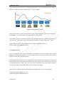
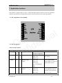
1
L70 Quectel GPS Engine Hardware Design L70_HD_V1.0 L70 Hardware Design Document Title L70 Hardware Design Revision 1.0 Date 2012-07-13 Status Released Document Control ID L70_HD_V1.0 l e t l c a i e t u n Q fide n o C General Notes Quectel offers this information as a service to its customers, to support application and engineering efforts that use the products designed by Quectel. The information provided is based upon requirements specifically provided for customers of Quectel. Quectel has not undertaken any independent search for additional information, relevant to any information that may be in the customer’s possession. Furthermore, system validation of this product designed by Quectel within a larger electronic system remains the responsibility of the customer or the customer’s system integrator. All specifications supplied herein are subject to change. Copyright This document contains proprietary technical information of Quectel Co., Ltd. Copying of this document, distribution to others, and communication of the contents thereof, are forbidden without permission. Offenders are liable to the payment of damages. All rights are reserved in the event of a patent grant or registration of a utility model or design. All specification supplied herein are subject to change without notice at any time. Copyright © Quectel Wireless Solutions Co., Ltd. 2012 L70_HD_V1.0 -1- L70 Hardware Design Contents Contents ............................................................................................................................................ 2 Table Index........................................................................................................................................ 4 Figure Index ...................................................................................................................................... 5 0. Revision history ............................................................................................................................ 6 1. Introduction ................................................................................................................................... 7 1.1. Related documents .............................................................................................................. 7 1.2. Terms and abbreviations ...................................................................................................... 7 2. Product concept............................................................................................................................. 9 2.1. Key features ........................................................................................................................ 9 2.2. Block diagram ................................................................................................................... 10 2.3. Evaluation board ............................................................................................................... 11 2.4. New technology................................................................................................................. 11 2.4.1. EASY technology .................................................................................................... 11 2.4.2. AlwaysLocateTM mode ............................................................................................ 11 2.4.3. Multi-tone AIC ........................................................................................................ 12 2.5. Protocol ............................................................................................................................. 13 3. Application interface ................................................................................................................... 14 3.1. Pin assignment of the module ........................................................................................... 14 3.2. Pin description ................................................................................................................... 14 3.3. Operating modes ............................................................................................................... 16 3.4. Power supply ..................................................................................................................... 16 3.5. Turn on and Turn off ......................................................................................................... 17 3.5.1. Turn on .................................................................................................................... 17 3.5.2. Turn off.................................................................................................................... 17 3.5.3. Restart...................................................................................................................... 17 3.6. Power saving mode ........................................................................................................... 18 3.6.1. Standby mode .......................................................................................................... 18 3.6.2. Back up mode .......................................................................................................... 18 3.6.3. Periodic standby mode ............................................................................................ 20 3.6.4. AlwaysLocateTM standby mode ............................................................................... 21 3.7. UART interface ................................................................................................................. 21 3.8. ANTON ............................................................................................................................. 22 4. Antenna interface ........................................................................................................................ 24 4.1. Antenna ............................................................................................................................. 24 4.2. Antenna supply .................................................................................................................. 24 4.2.1. Passive antenna with external LNA......................................................................... 24 4.2.2. Active antenna without external LNA ..................................................................... 25 4.2.3. Active antenna with external LNA .......................................................................... 26 5. Electrical, reliability and radio characteristics ............................................................................ 27 5.1. Absolute maximum ratings................................................................................................ 27 5.2. Operating conditions ......................................................................................................... 27 l e t l c a i e t u n Q fide n o C L70_HD_V1.0 -2- L70 Hardware Design 5.3. Current consumption ......................................................................................................... 28 5.4. Electro-static discharge ..................................................................................................... 28 5.5. Reliability test ................................................................................................................... 29 6. Mechanics ................................................................................................................................... 30 6.1. Mechanical view of the module ........................................................................................ 30 6.2. L70 Bottom dimension and recommended footprint......................................................... 30 6.3. Top view of the module .................................................................................................... 31 6.4. Bottom view of the module ............................................................................................... 32 7. Manufacturing ............................................................................................................................. 33 7.1. Assembly and soldering .................................................................................................... 33 7.2. Moisture sensitivity ........................................................................................................... 33 7.3. ESD safe ............................................................................................................................ 34 7.4. Tape and reel ..................................................................................................................... 34 l e t l c a i e t u n Q fide n o C L70_HD_V1.0 -3- L70 Hardware Design Table Index TABLE 1: RELATED DOCUMENTS ..................................................................................................... 7 TABLE 2: TERMS AND ABBREVIATIONS ......................................................................................... 7 TABLE 3: MODULE KEY FEATURES .................................................................................................. 9 TABLE 4: THE PROTOCOL SUPPORTED BY THE MODULE ........................................................ 13 TABLE 5: PIN DESCRIPTION ............................................................................................................. 14 TABLE 6: OVERVIEW OF OPERATING MODES.............................................................................. 16 l e t l c a i e t u n Q fide n o C TABLE 7: THE WAYS OF ENTERING AND EXITING FROM STANDBY MODE ......................... 18 TABLE 8: PIN DEFINITION OF THE V_BCKP PIN .......................................................................... 19 TABLE 9: PIN DEFINITION OF THE UART INTERFACES.............................................................. 21 TABLE 10: PIN DEFINITION OF THE ANTON ................................................................................. 23 TABLE 11: ANTENNA SPECIFICATION FOR L70 MODULE .......................................................... 24 TABLE 12: ABSOLUTE MAXIMUM RATINGS................................................................................. 27 TABLE 13: THE MODULE POWER SUPPLY RATINGS ................................................................... 27 TABLE 14: THE MODULE CURRENT CONSUMPTION (PASSIVE ANTENNA) .......................... 28 TABLE 15: THE ESD ENDURANCE TABLE (TEMPERATURE: 25℃, HUMIDITY: 45 %) ........... 28 TABLE 16: RELIABILITY TEST ......................................................................................................... 29 L70_HD_V1.0 -4- L70 Hardware Design Figure Index FIGURE 1: MODULE BLOCK DIAGRAM ......................................................................................... 10 FIGURE 2: ALWAYSLOCATETM MODE ............................................................................................. 12 FIGURE 3: REFERENCE RESET CIRCUIT USING OC CIRCUIT ................................................... 17 FIGURE 4: REFERENCE RESET CIRCUIT USING BUTTON .......................................................... 17 FIGURE 5: TIMING OF RESTARTING SYSTEM .............................................................................. 18 FIGURE 6: RTC SUPPLY FROM NON-CHARGEABLE BATTERY OR CAPACITOR .................... 19 FIGURE 7: REFERENCE CHARGING CIRCUIT FOR CHARGEABLE BATTERY ........................ 19 l e t l c a i e t u n Q fide n o C FIGURE 8: SEIKO XH414H-IV01E CHARGE CHARACTERISTIC ................................................. 20 FIGURE 9: PERIODIC MODE ............................................................................................................. 20 FIGURE 10: CONNECTION OF SERIAL INTERFACES ................................................................... 21 FIGURE 11: RS-232 LEVEL SHIFT CIRCUIT .................................................................................... 22 FIGURE 12: ANTON CONTROL CIRCUIT ........................................................................................ 23 FIGURE 13: TIMING OF EXTINT0 AND ANTON ............................................................................. 23 FIGURE 14: REFERENCE DESIGN FOR PASSIVE ANTENNA WITH LNA................................... 25 FIGURE 15: REFERENCE DESIGN FOR ACTIVE ANTENNA WITHOUT LNA ............................ 26 FIGURE 16: REFERENCE DESIGN FOR ACTIVE ANTENNA WITH LNA .................................... 26 FIGURE 17: L70 TOP VIEW AND SIDE VIEW(UNIT:MM) ......................................................... 30 FIGURE 18: L70 BOTTOM DIMENSION(UNIT:MM) .................................................................. 30 FIGURE 19: FOOTPRINT OF RECOMMENDATION(UNIT:MM)............................................... 31 FIGURE 20: TOP VIEW OF THE MODULE ....................................................................................... 31 FIGURE 21: BOTTOM VIEW OF THE MODULE .............................................................................. 32 FIGURE 22: RAMP-SOAK-SPIKE-REFLOW OF FURNACE TEMPERATURE .............................. 33 FIGURE 23: TAPE AND REEL SPECIFICATION ............................................................................... 34 L70_HD_V1.0 -5- L70 Hardware Design 0. Revision history Revision Date Author Description of change 1.0 2012-07-10 King HAO Initial l e t l c a i e t u n Q fide n o C L70_HD_V1.0 -6- L70 Hardware Design 1. Introduction This document defines and specifies L70 GPS module. It describes L70 hardware interface and its external application reference circuits, mechanical size and air interface. This document can help customer quickly understand the interface specifications, electrical and mechanical details of L70 module. With the help of this document and other related documents, customer can use L70 module to design and set up applications easily. l e t l c a i e t u n Q fide n o C 1.1. Related documents Table 1: Related documents SN [1] [2] [3] Document name Remark L70_EVB _UGD L70 EVB User Guide L70_GPS_Protocol L70 GPS Protocol Specification L70_Reference_Design L70 Reference Design 1.2. Terms and abbreviations Table 2: Terms and abbreviations Abbreviation Description AGPS Assisted GPS AIC Active Interference Cancellation CEP Circular Error Probable DGPS Differential GPS EASY Embedded Assist System EGNOS European Geostationary Navigation Overlay Service EMC Electromagnetic Compatibility EPO ESD GPS Extended Prediction Orbit Electrostatic Discharge Global Positioning System GNSS Global Navigation Satellite System GGA GPS Fix Data GLL Geographic Position – Latitude/Longitude GSA GNSS DOP and Active Satellites GSV GNSS Satellites in View HDOP Horizontal Dilution of Precision IC Integrated Circuit L70_HD_V1.0 -7- L70 Hardware Design I/O Input /Output Kbps Kilo Bits Per Second LNA Low Noise Amplifier MSAS Multi-Functional Satellite Augmentation System NMEA National Marine Electronics Association PDOP Position Dilution of Precision PMTK MTK Proprietary Protocol PPS Pulse Per Second PRN Pseudo Random Noise Code QZSS Quasi-Zenith Satellite System l e t l c a i e t u n Q fide n o C RHCP Right Hand Circular Polarization RMC Recommended Minimum Specific GNSS Data RTCM Radio Technical Commission for Maritime Services SBAS Satellite-based Augmentation System SAW Surface Acoustic Wave TTFF Time To First Fix UART Universal Asynchronous Receiver & Transmitter VDOP Vertical Dilution of Precision VTG Course over Ground and Ground Speed, Horizontal Course and Horizontal Velocity WAAS Wide Area Augmentation System Inom Nominal Current Imax Maximum Load Current Vmax Maximum Voltage Value Vnom Nominal Voltage Value Vmin Minimum Voltage Value VIHmax Maximum Input High Level Voltage Value VIHmin Minimum Input High Level Voltage Value VILmax Maximum Input Low Level Voltage Value VILmin Minimum Input Low Level Voltage Value VImax Absolute Maximum Input Voltage Value VImin Absolute Minimum Input Voltage Value VOHmax Maximum Output High Level Voltage Value VOHmin Minimum Output High Level Voltage Value VOLmax Maximum Output Low Level Voltage Value VOLmin Minimum Output Low Level Voltage Value L70_HD_V1.0 -8- L70 Hardware Design 2. Product concept The L70 GPS module brings the high performance of the MTK positioning engine to the industrial applications. It is able to achieve the industry’s highest level of sensitivity, accuracy and TTFF with the lowest power consumption in a small-footprint lead-free package. With 66 search channels and 22 simultaneous tracking channels, it acquires and tracks satellites in the shortest time even at indoor signal level. The embedded flash memory provides capacity for storing user-specific configurations and allows for future updates. l e t l c a i e t u n Q fide n o C The L70 module combines with many advanced features including AlwaysLocateTM , EASYTM, and AIC. These features are beneficial to reduce consumption and accelerate TTFF for L70 module. The module supports various location, navigation and industrial applications including autonomous GPS, SBAS (including WAAS, EGNOS, MSAS, and GAGAN), QZSS, and AGPS. The L70 is an SMD type module with the compact 10.1mm x 9.7mm x 2.5mm form factor, which can be embedded in customer applications through the 18-pin pads. It provides necessary hardware interfaces between the module and customer’s board. The module is fully RoHS compliant to EU regulation. 2.1. Key features Table 3: Module key features Feature Implementation Power supply Power consumption (passive antenna) Single supply voltage: 2.8V~4.3V Acquisition Tracking Standby Receiver Type GPS L1 1575.42MHz C/A Code 66 search channels, 22 simultaneous tracking channels Sensitivity Cold Start Reacquisition Hot start Tracking -145dBm -157 dBm -157 dBm -160 dBm Sensitivity (with external LNA) Cold Start Reacquisition Hot Start Tracking -148 dBm -160 dBm -160 dBm -163 dBm Time-To-First-Fix(EASY enabled) Cold Start Warm Start Hot Start 15s average@-130dBm 5s average@-130dBm 1s @-130dBm L70_HD_V1.0 typical : 3.3V 25mA@-130dBm 22mA@-130dBm 0.5mA@VCC=3.3V -9- L70 Hardware Design Cold Start (Autonomous) 35s average@-130dBm Warm Start (Autonomous) 30s average@-130dBm Hot Start (Autonomous) 1s@-130dBm Horizontal Position Accuracy(@-130dBm) <2.5 m CEP Max Update Rate Up to 10Hz,1Hz by default Accuracy of 1PPS Signal Typical accuracy <15ns (Not support time service) Time pulse width 100ms Velocity Accuracy Without Aid 0.1 m/s Acceleration Accuracy Without Aid 0.1 m/s² Time-To-First-Fix(EASY disabled) l e t l c a i e t u n Q fide n o C Dynamic Performance UART Port Maximum Altitude Maximum Velocity 515 m/s Maximum Acceleration 4G UART Port: TXD1 and RXD1 Supports baud rate from 4800bps to 115200bps,9600bps with default UART Port is used for NMEA output, MTK proprietary messages input and firmware upgrade 18,000 m Temperature range Physical Characteristics Size: 10.1±0.15 x 9.7±0.15 x 2.5±0.15mm Weight: Approx. 0.6g Normal operation: -40°C ~ +85°C Storage temperature: -45°C ~ +125°C 2.2. Block diagram The following figure shows a block diagram of L70 module. It consists of a single chip GPS IC which includes RF part and Baseband part, a SAW filter, a TCXO and a crystal oscillator. RF_IN Saw filter RF Front-End Integrated LNA Fractional-N Syntheszer Active Interference Cancellation Integrated LDO &PMU VCC VCC_RF V_BCKP GPS Engine TCXO UART Peripheral controller ROM RAM ARM7 Processor Serial Flash NRESET EXTINT 1PPS ANTON RTC 32.768K XTAL Figure 1: Module block diagram L70_HD_V1.0 - 10 - L70 Hardware Design 2.3. Evaluation board In order to help customers on the application of L70 module, Quectel supplies an Evaluation Board (EVB) with appropriate power supply, RS-232 serial cable, active antenna and other peripherals to test the module. For more details, please refer to the document [1]. 2.4. New technology l e t l c a i e t u n Q fide n o C 2.4.1. EASY technology By Supplying aided information like ephemeris, almanac, rough last position and time, and satellite status,AGPS can help improve GPS receiver TTFF and the acquisition sensitivity. The L70 module supports EASY technology which is one kind of AGPS. EASY works as an embedded software which can accelerate TTFF by predicting satellite navigation messages from received ephemeris. The GPS engine will calculate and predict orbit information automatically up to 3 days after first receiving the broadcast ephemeris, and saving the predicted information into the internal memory. GPS engine will use these information for positioning if no enough information from satellites, so the function will be helpful for positioning and TTFF improvement under indoor and urban condition. The EASY function can reduce TTFF to 5s for warm start. In this case, the backup power which supplies power for the RTC circuit is necessary. If no backup power, L70 module cannot store the extended ephemeris information and predict orbit information, in other words, it will become the cold start. Although the EASY also can accelerate TTFF in cold start, the backup power is still strongly recommended. In order to gain enough broadcast ephemeris information from GPS satellites, the GPS module should receive the information for at least 5 minutes in the good signal condition after it turned on. EASYTM function is enabled by default. The command “$PMTK869,0*29” can be used to query the status of EASY. If EASY is enabled, the module returns “ $PMTK869,2,1*36”, else returns “$PMTK869,2,0*37”. 2.4.2. AlwaysLocateTM mode AlwaysLocateTM is an intelligent controller of L70 normal mode and sleep mode. It is one of the power saving modes. According to the environmental and motion conditions, L70 can adaptively adjust the on/off time to achieve the balance between positioning accuracy and power consumption. L70_HD_V1.0 - 11 - L70 Hardware Design The following picture has shown the rough relationship between power consumption and the different scenarios in daily life when the AlwaysLocateTM mode is enabled. l e t l c a i e t u n Q fide n o C Figure 2: AlwaysLocateTM mode The position accuracy in AlwaysLocateTMmode will be somewhat degraded, especially in high speed. So this mode is not recommended in the applications of vehicle system. AlwaysLocateTMmode is disabled by default. Using the MTK proprietary commands can enable the AlwaysLocateTMmode. Please refer to the following commands to set the AlwaysLocateTM mode. Enable AlwaysLocateTM mode: $PMTK225,8*23;Return: $PMTK001,225,3*33 Back to normal mode: $PMTK225,0*2B 2.4.3. Multi-tone AIC Up to 12 multi-tone AIC (Active interference Cancellation) can provide effective narrow-band interference and jamming elimination. The GPS signal could be recovered from the jammed signal, which can ensure better navigation quality. Because different applications (Wi-Fi, GSM/GPRS, 3G/4G, Bluetooth) are integrated into navigation system, the harmonic of RF signal will influence the GPS reception. The multi-tone AIC can reject external RF interference which comes from other active components on the main board, to improve the capacity of GPS reception without any hardware change in the design. AIC function is enabled by default. The following commands can be used to set AIC function. Enable AIC function: $PMTK 286,1*23 Disable AIC function: $PMTK 286,0*22 L70_HD_V1.0 - 12 - L70 Hardware Design 2.5. Protocol The module supports standard NMEA-0813 protocol and MTK proprietary protocol (PMTK messages) that can be used to provide extended capabilities for many applications. The module is capable of supporting the following NMEA formats: GGA, GSA, GLL, GSV, RMC, VTG . Table 4: The protocol supported by the module Protocol NMEA PMTK Type Output, ASCII, 0183, 3.01 Input, MTK proprietary protocol l e t l c a i e t u n Q fide n o C Note: Please refer to document [2] about NMEA standard protocol and MTK proprietary protocol. L70_HD_V1.0 - 13 - L70 Hardware Design 3. Application interface The module is equipped with an 18-pin 1.1mm pitch SMT pad that connects to the user application platform. Sub-interfaces included in these pads are described in details in the following chapters. 3.1. Pin assignment of the module l e t l c a i e t u n Q fide n o C VRESET 9 VCC 8 NC 7 V_BCKP 6 EXTINT0 5 TIMEPULSE 4 NC RXD1 3 17 NC TXD1 2 18 RESERVED GND 1 10 GND 11 RF_IN 12 GND 13 ANTON 14 VCC_RF 15 RESERVED 16 L70 (Top View) 3.2. Pin description Table 5: Pin description Power Supply PIN NAME PIN NO. I/O DESCRIPTION DC CHARACTERISTICS COMMENT VCC 8 I Supply voltage Vmax= 4.3V Vmin=2.8V Vnom=3.3V Supply current of no less than 150mA. V_BCKP 6 I Backup voltage supply Vmax=4.3V Vmin=2.0V Vnom=2.8V IBCKP=7uA@Backup mode Power supply for RTC domain when VCC does not supply for the system. VCC_RF 14 O Output voltage RF section Vmax=4.3V Vmin=2.8V Vnom=3.3V Imax=50mA Usually supply for external active antenna or LNA. If unused, keep this pin open. VVCC_RF≈ VVCC Reset L70_HD_V1.0 - 14 - L70 Hardware Design PIN NAME PIN NO. I/O DESCRIPTION DC CHARACTERISTICS COMMENT VRESET 9 I System reset, low level active. VILmin=-0.3V VILmax=0.8V VIHmin=2.0V VIHmax=3.6V If unused, keep this pin open or connect it to the VCC. General purpose input/output PIN NAME PIN NO. I/O DESCRIPTION DC CHARACTERISTICS COMMENT EXTINT0 5 I External interrupt input VILmin=-0.3V VILmax=0.8V VIHmin=2.0V VIHmax= 3.6V This pin can be used to enter or exit from the standby mode. If unused, keep this pin open. Internally pulled up. O Time pulse VOLmin=-0.3V VOLmax=0.4V VOHmin=2.4V VOHmax=3.1V 1 pulse per second (1PPS). Synchronized at rising edge, the pulse width is100ms. If unused, keep this pin open. COMMENT l e t l c a i e t u n Q fide n o C TIMEPULSE 4 UART port PIN NAME PIN NO. I/O DESCRIPTION DC CHARACTERISTICS RXD1 3 I Receive data VILmin=-0.3V VILmax=0.8V VIHmin=2.0V VIHmax= 3.6V 2 O Transmit data VOLmin=-0.3V VOLmax=0.4V VOHmin=2.4V VOHmax=3.1V PIN NAME PIN NO. I/O DESCRIPTION DC CHARACTERISTICS COMMENT RF_IN 11 I GPS signal input Characteristic impedance of 50Ω Refer to chapter 4 13 O Active antenna or external LNA control pin in power standby mode The typical value is 2.8V. This pin can be used to control the power supply of the Active antenna or the enable pin of the external LNA in the standby mode. If unused, keep this pin open. TXD1 RF interface ANTON L70_HD_V1.0 - 15 - L70 Hardware Design 3.3. Operating modes The table below briefly summarizes the various operating modes of L70 module. Table 6: Overview of operating modes Mode Function Acquisition mode The module starts to search satellite, determine visible satellites and coarse carrier frequency and code phase of satellite signals. When the acquisition is completed, it switches to tracking mode automatically. The module refines acquisition’s message, as well as keeps tracking and demodulating the navigation data from the specific satellites. l e t l c a i e t u n Q fide n o C Tracking mode Standby mode Power saving mode Using EXTINT0 pin or PMTK command can make the module enter the standby mode. In this mode, the UART port is still accessible, but has no NEMA messages output, the current consumption of the module is also minimal. Backup mode When cutting off the main power supply, the module will enter the backup mode. In this mode, the RTC (Real Time Clock) power supply is needed. It can supply power for backed-up memory which contains all the necessary GPS information for quick start-up and a small amount of user configuration variables. Periodic standby mode Periodic standby mode is a periodic mode that can control the on/off time of L70 module periodically to reduce power consumption. It supports the module to switch automatically between normal mode and standby mode. AlwaysLocateTM standby mode AlwaysLocateTM is an intelligent controller of L70 periodic mode. AlwaysLocateTM standby mode supports the module to switch automatically between normal mode and standby mode. According to the environmental and motion conditions, the module can adaptively adjust the on/off time to achieve the balance between positioning accuracy and power consumption. 3.4. Power supply The main power supply is fed through the VCC pin. It is important that the system power supply circuitry is able to support the peak power. So the power supply must be able to provide sufficient current up to 150mA. The power supply of RTC circuit is fed through the V_BCKP pin. For more details, please refer to chapter 3.6.2. L70_HD_V1.0 - 16 - L70 Hardware Design 3.5. Turn on and Turn off 3.5.1. Turn on The module will be turned on when VCC is supplied. 3.5.2. Turn off Shutting down the module's main power supply is the only way to turn off the module. In this case, if the backup power is still present, the module will enter the backup mode. l e t l c a i e t u n Q fide n o C 3.5.3. Restart L70 module can be restarted by driving the VRESET to a low level voltage for a certain time and then releasing it. An OC driver circuit as shown below is recommended to control the VRESET. VRESET 4.7K Input pulse 47K Figure 3: Reference reset circuit using OC circuit The other way to control the VRESET pin is using a button directly. A TVS component needs to be placed close to the button for ESD protection. While pressing the key, ESD strike may generate from finger. A reference circuit is illustrated in Figure 4. S1 VRESET TVS1 Close to S1 Figure 4: Reference reset circuit using button L70_HD_V1.0 - 17 - L70 Hardware Design The restart timing has been illustrated in Figure 5. VCC <170ms Pulldown > 10ms VIH >2.0V VRESET (INPUT) VIL<0.8V l e t l c a i e t u n Q fide n o C Figure 5: Timing of restarting system 3.6. Power saving modes 3.6.1. Standby mode Standby mode is one of the power saving modes, in this mode, the UART serial port is still accessible, but has no NEMA messages output, the current consumption of the module is also minimal. The following table has shown the ways how to enter and exit from the standby mode. Table 7: The ways of entering and exiting from standby mode Mode Operation Changing the level of EXTINT0 pin from high to low. Enter the standby mode Sending the MTK proprietary command“$PMTK l61,0*28 ”. Changing the level of EXTINT0 pin from low to high. Exit from standby mode Sending any byte through the UART port. Note: Recommended to pull EXTINT0 pin high before turning on the module. 3.6.2. Back up mode When cutting off the main power supply, the module will enter the backup mode. In this mode, the RTC (Real Time Clock) power supply is needed. It can supply power for backed-up memory which contains all the necessary GPS information for quick start-up and a small amount of user configuration variables. The RTC power supply of module can be directly provided by an external capacitor or battery (rechargeable or non-chargeable) through the V_BCKP pin. L70_HD_V1.0 - 18 - L70 Hardware Design Table 8: Pin definition of the V_BCKP pin Name Pin No. Function V_BCKP 6 Backup voltage supply Note: The V_BCKP could not keep open. The V_BCKP pin should be connected to a battery or a capacitor for GPS module warm/hot start and AGPS. Please refer to the following figure for RTC backup: l e t l c a i e t u n Q fide n o C MODULE V_BCKP RTC LDO Non-chargeable battery or capacitor Figure 6: RTC supply from non-chargeable battery or capacitor The V_BCKP pin does not implement charging for rechargeable battery. It is necessary to add a charging circuit for rechargeable battery, shown as the following figure: VCC 1K Charge Circuit MODULE V_BCKP RTC LDO Chargeable Backup Battery Figure 7: Reference charging circuit for chargeable battery Coin-type Capacitor backup Coin-type Rechargeable Capacitor such as XH414H-IV01E from Seiko can be used. L70_HD_V1.0 - 19 - L70 Hardware Design l e t l c a i e t u n Q fide n o C Figure 8: Seiko XH414H-IV01E charge characteristic 3.6.3. Periodic standby mode Periodic standby mode is a periodic mode that can control the on/off time of L70 module periodically to reduce power consumption. It supports the module switches automatically between normal mode and standby mode. The following figure has shown the operation of periodic mode. Figure 9: Periodic mode Sending PMTK command can enter periodic standby mode. The ratio of run time and sleep time can be set by the command. For more details, please refer to document [2] about the MTK proprietary protocol. L70_HD_V1.0 - 20 - L70 Hardware Design 3.6.4. AlwaysLocateTM standby mode AlwaysLocateTM is an intelligent controller of L70 normal mode and standby mode. AlwaysLocateTM standby mode supports the module to switch automatically between normal mode and standby mode. According to the environmental and motion conditions, the module can adaptively adjust the on/off time to achieve the balance between positioning accuracy and power consumption. For more details, please refer to chapter 2.4.2. l e t l c a i e t u n Q fide n o C 3.7. UART interface The module provides one universal asynchronous receiver & transmitter serial port. The module is designed as a DCE (Data Communication Equipment), following the traditional DCE-DTE (Data Terminal Equipment) connection. The module and the client (DTE) are connected through the following signal shown as Figure 10. It supports data baud-rate from 4800bps to 115200bps. UART port TXD1: Send data to the RXD signal line of DTE RXD1: Receive data from the TXD signal line of DTE Table 9: Pin definition of the UART interfaces Interface UART Port Name Pin No. Function TXD1 2 Transmit data RXD1 3 Receive data MODULE (DCE) Serial port CUSTOMER (DTE) TXD1 TXD RXD1 RXD GND GND Figure 10: Connection of serial interfaces This UART port has the following features: UART port can be used for firmware upgrade, NMEA output and PMTK proprietary messages L70_HD_V1.0 - 21 - L70 Hardware Design input. The default output NMEA type setting is RMC, VTG, GGA, GSA, GSV, GLL. UART port supports the following data rates: 4800, 9600, 14400, 19200, 38400, 57600, 115200. The default setting is 9600bps, 8 bits, no parity bit, 1 stop bit . Hardware flow control and synchronous operation are not supported. The UART port does not support the RS-232 level but only supports the CMOS level. If the module’s UART port is connected to the UART port of a computer, it is necessary to add a level shift circuit between the module and the computer. Please refer to the following figure. l e t l c a i e t u n Q fide n o C 28 25 1 3 TXD1 Module 3.3V V+ C1- GND C2+ VCC C2- V- 24 23 22 19 T1IN T2IN T3IN T4IN 17 T5IN 16 21 20 18 RXD1 C1+ 13 /R1OUT R1OUT R2OUT R3OUT T4OUT T2OUT T3OUT T1OUT T5OUT R1IN R2IN R3IN 27 2 26 3.3V 4 10 6 7 5 12 8 9 11 ONLINE 15 /STATUS 14 /SHUTDOWN 6 7 8 9 To PC serial port 1 2 3 4 5 GND Figure 11: RS-232 level shift circuit 3.8. ANTON The ANTON is an optional pin which can be used to control the power supply of active antenna or the enable pin of the external LNA. The recommended circuit diagram is shown in Figure 12. When L70 module enters the standby mode, the ANTON pin will be pulled down, the Q1 and Q2 are in high impedance state and the power supply for antenna is cut off. In normal mode, the voltage value of ANTON is about 2.8V, it will make Q1 and Q2 in the on-state, then VCC_RF will provide power supply for the active antenna. Figure 13 has shown the timing between the ANTON pin and the EXTINT0 pin. L70_HD_V1.0 - 22 - L70 Hardware Design Table 10: Pin definition of the ANTON Name Pin No. Function ANTON 13 Control the power supply of the active GPS antenna or the enable pin of the external LNA. Active Antenna L70_Module LNA RF_IN EN VCC l e t l c a i e t u n Q fide n o C L1 47nH R3 100R R1 10R ANTON Q1 Q2 R2 10K VCC_RF Figure 12: ANTON control circuit Figure 13: Timing of EXTINT0 and ANTON L70_HD_V1.0 - 23 - L70 Hardware Design 4. Antenna interface The L70 module receives L1 band signal from GPS satellites at a nominal frequency of 1575.42MHz. The RF signal is connected to the RF_IN pin. Customer should use a controlled impedance transmission line of 50 Ohm to connect to RF_IN. 4.1. Antenna L70 module can be connected to passive or active antenna. l e t l c a i e t u n Q fide n o C Table 11: Antenna specification for L70 module Antenna type Specification Passive antenna Center frequency: Band Width: Gain: Polarization: Active antenna Center frequency: Band Width: Minimum gain: Maximum noise figure: Maximum gain: Polarization: 1575.42 MHz >20 MHz >0 dBi RHCP or Linear 1575.42 MHz >5 MHz 15-20dB(compensate signal loss in RF cable) 1.5dB 50dB RHCP or Linear 4.2. Antenna supply 4.2.1. Passive antenna with external LNA Typically a design using a passive antenna requires more attention regarding the layout of the RF section. An external LNA between the passive antenna and the L70 module is strongly recommended to add for improving receiver sensitivity. It is always beneficial to reserve a П or L passive matching network between the passive antenna and the LNA. Figure14 is the rough reference design. For more details, please refer to document [3]. L70_HD_V1.0 - 24 - L70 Hardware Design Passive Antenna BGA715L7 R1 0R C1 NM C2 NM П matching circuit R2 150R RF_IN EN vcc LNA L70_Module R3 100R ANTON VCC_RF l e t l c a i e t u n Q fide n o C Figure 14: Reference design for passive antenna with LNA Note: VCC_RF is directly connected to the power supply of L70 module internally. If VCC_RF is not suitable to the external LNA, using R2 as a divider or adding an external LDO circuit to get the required voltage. R3 is used as a current limiting resistor. 4.2.2. Active antenna without external LNA Active antenna could be connected to RF_IN directly and you also can reserve a П or L passive matching network between the active antenna and the L70 module. If an active antenna is connected to RF_IN, the integrated low-noise amplifier of the antenna must be powered by an external correct supply voltage. Generally, the supply voltage is fed to the antenna through the coaxial RF cable. An active antenna’s loading current is between 5mA to 20mA. The inductor L1 outside of the module prevents the RF signal from leaking into the VCC_RF pin and routes the bias supply to the active antenna. Please refer to the reference circuit shown in Figure 15. If the VCC_RF voltage does not meet the requirements for powering the active antenna, an external LDO could be used. L70_HD_V1.0 - 25 - L70 Hardware Design Active Antenna П matching circuit L70_Module C1 NM C2 NM R3 0R RF_IN 10R L1 47nH R1 ANTON R2 10K Q1 Q2 VCC_RF l e t l c a i e t u n Q fide n o C Figure 15: Reference design for active antenna without LNA Note: The rated power of resistor R1 should be chosen no less than 1 watt in case active antenna is shorted unexpectedly. In order to reduce consumption, the value of resistor R2 is not recommended to choose too small. 4.2.3. Active antenna with external LNA In order to obtain better receiver sensitivity, an active antenna and an external LNA are recommended. You also can reserve a П or L passive matching network between the active antenna and the LNA. The rough reference circuit is shown in Figure16. For more details, please refer to document [3]. Active Antenna П matching circuit C1 NM C2 NM L70_Module LNA R3 0R EN VCC RF_IN R4 R5 L1 R1 Q1 Q2 R2 ANTON VCC_RF Figure 16: Reference design for active antenna with LNA L70_HD_V1.0 - 26 - L70 Hardware Design 5. Electrical, reliability and radio characteristics 5.1. Absolute maximum ratings Absolute maximum rating for power supply and voltage on digital pins of the module are listed in Table 12. Table 12: Absolute maximum ratings l e t l c a i e t u n Q fide n o C Parameter Min Max Unit Power supply voltage (VCC) -0.3 4.3 V Backup battery voltage (V_BCKP) -0.3 4.3 V Input voltage at digital pins -0.3 3.6 V VCC_RF output current (Ivccrf) 50 mA Input power at RF_IN (Prfin) 0 dBm 125 °C -45 Storage temperature Note: Stressing the device beyond the “Absolute Maximum Ratings” may cause permanent damage. These are stress ratings only. The product is not protected against over voltage or reversed voltage. If necessary, voltage spikes exceeding the power supply voltage specification, given in table above, must be limited to values within the specified boundaries by using appropriate protection diodes. 5.2. Operating conditions Table 13: The module power supply ratings Parameter Description Conditions Min Typ Max Unit VCC Supply voltage Voltage must stay within the min/max values, including voltage drop, ripple, and spikes. 2.8 3.3 4.3 V IVCCP* Peak supply current VCC=3.3V 150 mA V_BCKP Backup voltage supply 4.3 V VCC_RF Output voltage RF section VCC V IVCC_RF VCC_RF output current 50 mA TOPR Normal Operating temperature 85 ℃ L70_HD_V1.0 2.0 -40 3.3 25 - 27 - L70 Hardware Design * This figure can be used to determine the maximum current capability of power supply. Note: Operation beyond the "Operating Conditions" is not recommended and extended exposure beyond the "Operating Conditions" may affect device reliability. 5.3. Current consumption The values for current consumption are shown in Table 14. Table 14: The module current consumption (passive antenna) l e t l c a i e t u n Q fide n o C Parameter Condition Min Typ Max Unit Icc @Acquisition @-130dBm 25 mA Icc @Tracking @-130dBm(For Cold Start, 10 minutes after First Fix. For Hot Start, 15 seconds after First Fix.) 22 mA Icc @Standby @VCC=3.3V 0.5 mA IBCKP @backup @V_BCKP=3.3V 7 uA Note: In the standby mode, the power supply to active antenna through VCC_RF is cut off. It will be re-activated when the module exits from the standby mode. 5.4. Electro-static discharge L70 module is an ESD sensitive device. ESD protection precautions should still be emphasized. Proper ESD handing and packaging procedures must be applied throughout the processing, handing and operation of any application. The ESD bearing capability of the module is listed in Table 15. Note that the customer should add ESD components to module pins in the particular application except RF_IN, VCC and GND pins. Table 15: The ESD endurance table (Temperature: 25℃, Humidity: 45 %) Pin Contact discharge Air discharge VCC,GND ±5KV ±5KV ±10KV ±10KV UART ±3KV ±6KV Others ±2KV ±4KV RF_IN L70_HD_V1.0 - 28 - L70 Hardware Design 5.5. Reliability test Table 16: Reliability test Test term Condition Standard Thermal shock -30°C...+80°C, 144 cycles Damp heat, cyclic +55°C; >90% Rh 6 cycles for 144 hours Vibration shock 2 3 GB/T 2423.22-2002 Test Na IEC 68-2-14 Na 2 3 5~20Hz,0.96m /s ;20~500Hz,0.96m /s -3dB/oct, IEC 68-2-30 Db Test 2423.13-1997 Test Fdb l e t l c a i e t u n Q fide n o C Heat test 1hour/axis; no function IEC 68-2-36 Fdb Test 85°C, 2 hours, Operational GB/T 2423.1-2001 Ab IEC 68-2-1 Test Cold test -40°C, 2 hours, Operational GB/T 2423.1-2001 Ab IEC 68-2-1 Test Heat soak 90°C, 72 hours, Non-Operational GB/T 2423.2-2001 Bb IEC 68-2-2 Test B Cold soak -45°C, 72 hours, Non-Operational GB/T 2423.1-2001 A IEC 68-2-1 Test L70_HD_V1.0 - 29 - L70 Hardware Design 6. Mechanics This chapter describes the mechanical dimensions of the module. 6.1. Mechanical view of the module l e t l c a i e t u n Q fide n o C Figure 17: L70 Top view and Side view(Unit:mm) 6.2. L70 Bottom dimension and recommended footprint Figure 18: L70 Bottom dimension(Unit:mm) L70_HD_V1.0 - 30 - L70 Hardware Design Keep Out l e t l c a i e t u n Q fide n o C Figure 19: Footprint of recommendation(Unit:mm) Notes: 1. The keep-out area should be covered by solder mask and top silk layer for isolation between the top layer of host board and the bottom layer of the module. 2. For easy maintenance of this module and accessing to these pads, please keep a distance of no less than 3mm between the module and other components in host board. 6.3. Top view of the module 1 18 9 10 Figure 20: Top view of the module L70_HD_V1.0 - 31 - L70 Hardware Design 6.4. Bottom view of the module 18 1 l e t l c a i e t u n Q fide n o C 10 9 Figure 21: Bottom view of the module L70_HD_V1.0 - 32 - L70 Hardware Design 7. Manufacturing 7.1. Assembly and soldering L70 is intended for SMT assembly and soldering in a Pb-free reflow process on the top side of the PCB. It is suggested that the minimum height of solder paste stencil is 130um to ensure sufficient solder volume. Pad openings of paste mask can be increased to ensure proper soldering and solder wetting over pads. It is suggested that peak reflow temperature is 235~245ºC (for SnAg3.0Cu0.5 alloy). Absolute max reflow temperature is 260ºC. To avoid damage to the module when it is repeatedly heated, it is suggested that the module should be mounted after the first panel has been reflowed. The following picture is the actual diagram which we have operated. l e t l c a i e t u n Q fide n o C ℃ Preheat Heating Cooling 250 Liquids Temperature 217 200℃ 200 40s~60s 160℃ 150 70s~120s 100 Between 1~3℃/S 50 0 50 100 150 200 250 300 s Time(s) Figure 22: Ramp-soak-spike-reflow of furnace temperature 7.2. Moisture sensitivity L70 is sensitivity to moisture absorption. To prevent L70 from permanent damage during reflow soldering, baking before reflow is required in following cases: Humidity indicator card: At least one circular indicator is no longer blue The seal is opened and the module is exposed to excessive humidity. L70_HD_V1.0 - 33 - L70 Hardware Design L70 should be baked for 192 hours at temperature 40℃+5℃/-0℃ and <5% RH in low-temperature containers, or 24 hours at temperature 125℃±5℃ in high-temperature containers. Care should be taken that plastic tray is not heat resistant. L70 should be taken out before preheating, otherwise, the tray maybe damaged by high-temperature heating. 7.3. ESD safe L70 module is an ESD sensitive device and should be careful to handle. 7.4. Tape and reel l e t l c a i e t u n Q fide n o C Out direction Unit: mm Figure 23: Tape and reel specification L70_HD_V1.0 - 34 - Shanghai Quectel Wireless Solutions Co., Ltd. Room 501, Building 13, No.99, TianZhou Road, Shanghai, China 200233 Tel: +86 21 5108 6236 Mail: [email protected]