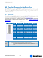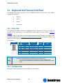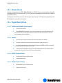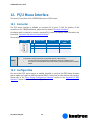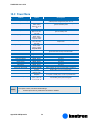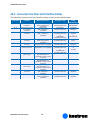
1
T-MOPSlcdSA User’s Guide Document Revision 1.2 T-MOPSlcdSA User's Guide Contents 1. USER INFORMATION ..............................................................................................1 1.1 1.2 1.3 1.4 1.5 1.6 About This Manual .....................................................................................1 Copyright Notice .......................................................................................1 Trademarks ..............................................................................................2 Standards ................................................................................................2 Warranty..................................................................................................2 Technical Support ......................................................................................3 2. INTRODUCTION .....................................................................................................4 2.1 2.2 2.3 T-MOPSlcdSA ............................................................................................4 The MOPS Family........................................................................................5 PC/104 an Embedded PC Standard.................................................................6 3. GETTING STARTED ..................................................................................................7 4. SPECIFICATIONS....................................................................................................8 4.1 4.2 4.2.1 4.2.2 4.2.3 4.2.4 4.3 4.3.1 4.3.2 4.3.3 4.3.4 4.3.5 4.4 4.5 4.5.1 4.5.2 Functional Specifications ............................................................................8 Mechanical Specifications ...........................................................................9 PC/104 Bus Connector (ISA part) ..................................................................9 Module Dimensions ....................................................................................9 Height ....................................................................................................9 Weight ....................................................................................................9 Electrical Specifications ............................................................................ 10 Supply Voltage........................................................................................ 10 Supply Voltage Ripple ............................................................................... 10 Supply Current (typical DOS prompt)............................................................ 10 Supply Current (Maximum) ........................................................................ 10 External RTC Battery................................................................................. 10 MTBF..................................................................................................... 11 Environmental Specifications ..................................................................... 11 Temperature ........................................................................................... 11 Humidity ............................................................................................... 11 5. CPU, CHIPSET AND SUPER-I/O ...............................................................................12 5.1 5.2 5.3 5.4 CPU and Chipset ...................................................................................... 12 CPU and Chipset Configuration ................................................................... 12 Super I/O Controller................................................................................. 13 Super I/O Controller Configuration.............................................................. 13 6. SYSTEM MEMORY.................................................................................................14 6.1 Contents Configuration ......................................................................................... 14 i 1 T-MOPSlcdSA User's Guide 7. ISA AND PC/104 BUS EXPANSION...........................................................................15 7.1 7.1.1 7.1.2 7.2 PC/104 Bus (ISA part) .............................................................................. 15 PC/104 Connectors .................................................................................. 15 PC/104 Configuration ............................................................................... 16 PC/104 Stack .......................................................................................... 16 8. GRAPHICS INTERFACE ..........................................................................................17 8.1 8.2 8.3 8.4 8.5 Graphics Controller .................................................................................. 17 CRT Connector......................................................................................... 17 Configuration ......................................................................................... 17 Graphics Technical Support........................................................................ 17 Available Video Modes .............................................................................. 18 9. SERIAL-COMMUNICATION INTERFACES ....................................................................19 9.1 9.2 Connectors............................................................................................. 19 Configuration ......................................................................................... 19 10. PARALLEL-COMMUNICATION INTERFACE ..................................................................20 10.1 10.2 Connector .............................................................................................. 20 Configuration ......................................................................................... 21 11. KEYBOARD AND FEATURE INTERFACE.......................................................................22 11.1 11.2 11.3 11.4 11.4.1 11.4.2 11.4.3 11.4.4 11.4.5 11.4.6 Connector .............................................................................................. 22 Configuration ......................................................................................... 22 Known Issues.......................................................................................... 23 Signal Descriptions .................................................................................. 23 /RESIN and PWRGOOD (Reset Inputs) ........................................................... 23 Speaker ................................................................................................. 23 KBDAT (Keyboard Data)............................................................................. 23 KBCLK (Keyboard Clock) ............................................................................ 23 BATT (System Battery Connection)............................................................... 24 Example Connection AT-keyboard and Other Functions .................................... 24 12. PS/2 MOUSE INTERFACE ....................................................................................... 25 12.1 12.2 Connector .............................................................................................. 25 Configuration ......................................................................................... 25 13. USB INTERFACE................................................................................................... 26 13.1 13.2 13.3 Connector .............................................................................................. 26 Configuration ......................................................................................... 27 Limitations ............................................................................................ 27 14. IDE INTERFACE ................................................................................................... 28 14.1 14.2 Connector .............................................................................................. 28 Configuration ......................................................................................... 29 15. ETHERNET INTERFACE...........................................................................................30 Contents ii 2 T-MOPSlcdSA User's Guide 15.1 15.2 15.3 Connector .............................................................................................. 31 Configuration ......................................................................................... 31 Ethernet Technical Support........................................................................ 31 16. POWER CONNECTION............................................................................................ 32 16.1 16.2 16.3 16.4 Connector .............................................................................................. 32 Power Pins ............................................................................................. 32 External Battery ...................................................................................... 33 Configuration ......................................................................................... 33 17. WATCHDOG TIMER ...............................................................................................34 17.1 17.2 17.2.1 17.2.2 Configuration ......................................................................................... 34 Programming.......................................................................................... 34 Initialization .......................................................................................... 34 Trigger .................................................................................................. 34 18. APPENDIX A: SYSTEM RESOURCE ALLOCATIONS .........................................................35 18.1 18.2 18.3 18.4 18.4.1 Interrupt Request (IRQ) Lines..................................................................... 35 Direct Memory Access (DMA) Channels ......................................................... 36 I/O Address Map ...................................................................................... 37 Memory Map ........................................................................................... 38 Using Expanded Memory Managers .............................................................. 39 19. APPENDIX B: BIOS OPERATION...............................................................................40 19.1 19.2 19.2.1 19.2.2 19.3 19.4 19.4.1 19.4.2 19.4.3 19.4.4 19.4.5 19.4.6 19.5 19.6 19.6.1 19.7 19.8 19.8.1 19.8.2 19.8.3 19.8.4 19.9 19.10 Contents Determining BIOS Version ......................................................................... 40 Setup Guide (ezPORT) ............................................................................... 41 Start ezPORT BIOS Setup Utility................................................................... 41 General Information................................................................................. 41 Main Menu ............................................................................................. 44 Advanced Menu....................................................................................... 45 IDE Configuration Submenu ....................................................................... 45 Master or Slave Submenus ......................................................................... 46 Watchdog Submenu ................................................................................. 47 Remote Access Configuration ..................................................................... 47 USB Configuration Submenu ...................................................................... 48 USB Mass Storage Device Configuration Submenu........................................... 49 PCI PnP Menu.......................................................................................... 50 Boot Menu ............................................................................................. 52 Boot Settings Configuration Submenu.......................................................... 53 Security Menu ......................................................................................... 54 Chipset Menu.......................................................................................... 55 STPC Integrated IO Device Configuration Submenu.......................................... 56 Cache & Shadow Configuration Submenu ...................................................... 57 North Bridge Configuration Submenu........................................................... 58 ISA Bus Configuration Submenu.................................................................. 58 Power Menu............................................................................................ 59 Exit Menu............................................................................................... 60 iii 3 T-MOPSlcdSA User's Guide 19.11 19.11.1 19.11.2 19.11.3 19.11.4 19.12 19.12.1 19.12.2 19.12.3 Kontron BIOS Extensions........................................................................... 61 JIDA BIOS extension ................................................................................ 61 Remote Control Client Extension ................................................................. 61 LAN RPL ROM .......................................................................................... 62 DOT-Matrix LCD BIOS Extension................................................................... 62 Updating or Restoring BIOS ....................................................................... 63 Null modem cable .................................................................................... 63 BIOS Update or Recovery Step-by-Step ......................................................... 64 Terminal Programs................................................................................... 65 20. APPENDIX C: BLOCK DIAGRAM ...............................................................................66 21. APPENDIX D: MECHANICAL DIMENSIONS .................................................................67 22. APPENDIX E: CONNECTOR LAYOUT...........................................................................69 22.1 22.2 22.3 Connector Locations................................................................................. 69 Connector Functions and Interface Cables..................................................... 70 Pin-out Table .......................................................................................... 71 23. APPENDIX F: LIMITATIONS AND HINTS.....................................................................74 23.1 23.2 23.3 23.4 23.5 Unavailable ISA Signals ............................................................................ 74 USB Ports .............................................................................................. 74 USB Devices ........................................................................................... 74 Windows98 Support .............................................................................. 74 Keyboard Controller ................................................................................. 75 24. APPENDIX F: PC ARCHITECTURE INFORMATION ..........................................................76 24.1 24.1.1 24.1.2 24.2 24.3 24.3.1 24.3.2 24.3.3 24.4 Buses.................................................................................................... 76 ISA, Standard PS/2 - Connectors................................................................. 76 PC/104, PCI - Information ......................................................................... 76 General PC Architecture ............................................................................ 77 Ports..................................................................................................... 77 RS-232 Serial.......................................................................................... 77 ATA ...................................................................................................... 77 USB ...................................................................................................... 78 Programming.......................................................................................... 78 25. APPENDIX G: DOCUMENT-REVISION HISTORY ............................................................ 79 Contents iv 4 T-MOPSlcdSA User's Guide 1. User Information 1.1 About This Manual This document provides information about products from Kontron Embedded Modules GmbH and/or its subsidiaries. No warranty of suitability, purpose, or fitness is implied. While every attempt has been made to ensure that the information in this document is accurate, the information contained within is supplied “as-is” and is subject to change without notice. For the circuits, descriptions and tables indicated, Kontron assumes no responsibility as far as patents or other rights of third parties are concerned. 1.2 Copyright Notice Copyright © 2005-2007 Kontron Embedded Modules GmbH All rights reserved. No part of this manual may be reproduced, transmitted, transcribed, stored in a retrieval system, or translated into any language or computer language, in any form or by any means (electronic, mechanical, photocopying, recording, or otherwise), without the express written permission of Kontron Embedded Modules GmbH. DIMM-PC®, PISA®, ETX®, ETXexpress® , X-board®, DIMM-IO® and DIMM-BUS® are trademarks or registered trademarks of Kontron Embedded Modules GmbH. Kontron is trademark or registered trademark of Kontron AG. User Information 1 1 T-MOPSlcdSA User's Guide 1.3 Trademarks The following lists the trademarks of components used in this board. Microsoft is a registered trademark of Microsoft Corp. Intel is a registered trademark of Intel Corp. 1.4 IBM, XT, AT, PS/2 and Personal System/2 are trademarks of International Business Machines Corp. All other products and trademarks mentioned in this manual are trademarks of their respective owners. Standards Kontron Embedded Modules is certified to ISO 9000 standards. 1.5 Warranty This Kontron Embedded Modules product is warranted against defects in material and workmanship for the warranty period from the date of shipment. During the warranty period, Kontron Embedded Modules will at its discretion decide to repair or replace defective products. Within the warranty period, the repair of products is free of charge as long as warranty conditions are observed. The warranty does not apply to defects resulting from improper or inadequate maintenance or handling by the buyer, unauthorized modification or misuse, operation outside of the product’s environmental specifications or improper installation or maintenance. Kontron Embedded Modules will not be responsible for any defects or damages to other products not supplied by Kontron Embedded Modules that are caused by a faulty Kontron Embedded Modules product. User Information 2 2 T-MOPSlcdSA User's Guide 1.6 Technical Support Technicians and engineers from Kontron Embedded Modules and/or its subsidiaries and official distributors are available for technical support. We are committed to making our product easy to use and will help you use our products in your systems. Before contacting Kontron Embedded Modules technical support, please contact your local representative or consult our Web site for the latest product documentation, utilities, and drivers. If the information does not help to solve the problem, contact us by telephone or email. Asia Europe North/South America Kontron Asia Inc. Kontron Embedded Modules GmbH Kontron America 4F, No.415, Ti-Ding Blvd., NeiHu District, Taipei 114, Taiwan Brunnwiesenstr. 16 94469 Deggendorf – Germany Tel: +886 2 2799 2789 Fax: + 886 2 2799 7399 [email protected] Tel: +49 (0) 991-37024-0 Fax: +49 (0) 991-37024-333 [email protected] 14118 Stowe Dr Poway, CA 92064-7147 Customer Service/Technical Support: 800-480-0044 (US Only) Tel: +1 (888) 294 4558 Fax: +1 (858) 677 0898 [email protected] User Information 3 3 T-MOPSlcdSA User's Guide 2. Introduction 2.1 T-MOPSlcdSA The T-MOPSlcdSA comes with a STMicroelectronics STPC® Atlas embedded microcontroller. The ATLAS processor runs with an internal clock speed of 120MHz and is fully compatible with standard x86 processors. The processor is combined with a powerful chipset to provide a general purpose PC-compatible subsystem on a single chip. The CPU/chipset does not require a cooler or a fan. The T-MOPSlcdSA is equipped with 32MB SDRAM soldered onboard (64MB as option upon request), which makes this PC/104 processor board especially suitable for use in rugged environments. However, the standard product available on stock comes with 32MB of SDRAM. Every T-MOPSlcdSA comes with the PC/104 standard interface (full 16bit ISA signals). The T-MOPSlcdSA is a highly integrated CPU board that features many standard interfaces, including a watchdog timer and a real-time clock. The board integrates the complete functionality of an 80486 motherboard and includes the following features: CPU / chipset (single chip) System BIOS SDRAM controller, which supports up to 64MB SDRAM Interrupt controller and DMA controller EIDE controller The following features are provided via the onboard PCI bus (PCI 2.1 compliant): 32-bit PCI Ethernet controller Additional peripheral functions include: Keyboard controller and PS/2 mouse support Real-time clock Watchdog timer (WDT) Two serial ports (Both RS-232) Parallel port (SPP/EPP/ECP modes) USB 1.1 compatible OHCI 1.0 controller T-MOPSlcdSA online: http://emea.kontron.com/index.php?id=226&cat=54&productid=496. Introduction 4 4 T-MOPSlcdSA User's Guide 2.2 The MOPS Family MOPS (Minimized Open PC System) PC/104 products represent the “Proven PC Platform for Instant Solutions." Each MOPS module is characterized by the same pin out for the keyboard, COM1 and COM2, 44-pin IDE, LPT, and 1st LAN. These homogeneous features facilitate easy upgrades within the Kontron Embedded Modules GmbH MOPS PC/104 product family. Whenever a LCD panel is required, MOPS products with onboard graphics controllers serve as the right choice. Display connections are simplified when using these units, which come with a JUMPtec Intelligent LVDS Interface (JILI) and a JUMPtec Intelligent Panel Adapter (JIPA) interface. The two interfaces can recognize which display is connected and then independently set all video parameters. These interfaces are not available on all MOPS products. T-MOPSlcdSA provides a CRT output only but it can easily connect to a TFT by i.e. CRTtoLCD-5. More information can be obtained under the following product link to Kontron website: http://emea.kontron.com/index.php?id=226&cat=78&productid=1145. All MOPS-PC/104 are plug-and-work enabled to further reduce time-to-market. As part of the standard features package, all MOPS PC/104 modules come with a JUMPtec Intelligent Device Architecture (JIDA) interface, which is integrated into the BIOS of the PC/104 modules. This interface enables hardware-independent access to the MOPS-PC/104 features that cannot be accessed via standard APIs. Functions such as watchdog timer, brightness and contrast of LCD backlight, and user bytes in the EEPROM can be configured with ease by taking advantage of this standard MOPS PC/104 module feature. All MOPS PC/104 products can be controlled remotely by using JRC software through a serial port. The software allows you to change, update, and maintain the MOPS products from a host computer via a serial connection. General MOPS information is obtained here: http://www.kontron.com/mops You can find MOPS PC/104 accessories information here: http://emea.kontron.com/index.php?id=82&cat=56 You can find MOPS PC/104 Starterkit information here: http://emea.kontron.com/index.php?id=82&cat=57 Introduction 5 5 T-MOPSlcdSA User's Guide 2.3 PC/104 an Embedded PC Standard Over the past decade, PC architecture has become an accepted platform for far more than desktop applications. Dedicated and embedded applications for PCs are beginning to appear everywhere. By standardizing hardware and software around the broadly supported PC architecture, embedded system designers can substantially reduce development costs, risks, and time-to-market. For these reasons, companies that embed microcomputers as controllers within their products seek ways to reap the benefits of using the PC architecture. However, the standard form factor of a PC bus (12.4" x 4.8") and its associated card cages and backplanes are too bulky and expensive for most embedded control applications. The only practical way to embed the PC architecture in space-and power-sensitive applications has been to design a PC chip by chip directly into the product. But this runs counter to growing trend away from "reinventing the wheel." Whenever possible, top management now encourages outsourcing of components and technologies to reduce development costs and accelerate product design cycles. A need has arisen for a more compact implementation of the PC bus, satisfying the reduced space and power constraints of embedded control applications. PC/104 was developed in response to this need. It offers full architecture, hardware and software compatibility with the PC bus but in ultra-compact (3.6" x 3.8") stackable modules. PC/104 is ideally suited to the unique requirements of embedded control applications. Although configuration and application possibilities with PC/104 modules are practically limitless, there are two ways to use them in embedded system designs: Introduction Standalone module stacks PC/104 modules are self-stacking. The modules are used like ultra-compact bus boards but without a need for backplanes or card cages. Stacked modules are spaced 0.6 inches apart. (The three-module stack measures 3.6 by 3.8 by 2 inches.) Companies using PC/104 module stacks within their products frequently create one or more of their own applicationspecific PC/104 modules. Component-line applications In this configuration, the modules function as highly integrated components, plugged into custom carrier boards that contain application-specific interfaces and logic. The modules' self-stacking bus can be useful to install multiple modules in one location. This facilitates product upgrades or options and allows temporary addition of modules during system debug or test. 6 6 T-MOPSlcdSA User's Guide 3. Getting Started The easiest way to get the T-MOPSlcdSA board running is to use a starter kit from Kontron Embedded Modules GmbH. Take the following steps: 1. Turn off the power supply (part of the starter kit). 2. Connect the power supply to the starter kit baseboard (part of the starter kit). 3. Connect a CRT monitor to the CRT interface by using the corresponding adapter cable. 4. Plug the T-MOPSlcdSA to the PC/104 bus stack on the starter kit baseboard. 5. Make all necessary connections from the T-MOPSlcdSA to the starter kit board. (Cables come with the starter kit). The starter kit board offers various interfaces on standard connectors. 6. Plug a keyboard to the starter kit’s keyboard connector. 7. Plug a hard-drive data cable to the T-MOPSlcdSA hard-disk interface. Attach the hard disk to the connector at the opposite end of the cable. 8. If necessary, connect the power supply to the hard disk’s power connector. 9. Make sure all your connections have been made correctly. 10. Turn on the power. 11. Enter the BIOS by pressing the <DEL> key during boot-up. Make all changes in the BIOS setup. See the BIOS chapter of this manual for details. Getting Started 7 7 T-MOPSlcdSA User's Guide 4. Specifications 4.1 Functional Specifications Processor STMicroelectronics STPC® Atlas with 120 MHz internal clock and 8KB unified instruction and data cache (fanless) Chipset Integrated PCI North / South Bridge controller Power Supply 5V supply Memory Onboard soldered 32MB or 64MB SDRAM (60Mhz clock speed) Ethernet: Intel® 82551IT Network Controller 32-bit Fast Ethernet Integrated IEEE 802.3 10BASE-T and 100BASE-TX compatible PHY Backward compatible software to 82559ER controller worksaccording to the common criteria of the embedded technology market segment Two Serial Ports, (COM1 and COM2) Standard RS232C serial ports with 16-bit FIFO 15540 compatible Parallel Port (LPT) All IEEE Standard 1284 protocols supported: Compatibility, Nibble, Byte, EPP and ECP modes Integrated USB Controller Two USB OHCI 1.0 compliant ports USB 1.1 compatible EIDE Hard-disk Interface Support for PIO mode 3 & 4 Supports up to two devices Individual drive timing for all two devices Backward compatibility with IDE (ATA-1) Supports Kontron chipDISK Watchdog Timer 256KB Flash BIOS (AMI) Specifications 8 8 T-MOPSlcdSA User's Guide Real-time Clock External battery support Keyboard Controller Internal Graphics Controller VGA and SVGA CRT Controller 135MHz RAMDAC Enhanced 2D Graphics engine The frame buffer can occupy a space up to 4 Mbytes anywhere in the physical main memory PC/104 Extension Bus 4.2 Mechanical Specifications 4.2.1 PC/104 Bus Connector (ISA part) 4.2.2 Module Dimensions 4.2.3 95 x 90 mm (3.7” x 3.5”) Height 4.2.4 One 2 X 32 pin stack-through and one 2 X 20 pin stack-through connector 23.5 mm max (including PC/104 connector pins) Weight Specifications 85 g (full feature version) 9 9 T-MOPSlcdSA User's Guide 4.3 Electrical Specifications 4.3.1 Supply Voltage 4.3.2 Supply Voltage Ripple 4.3.3 4.3.4 T-MOPSlcdSA with 32MB SDRAM: Power Mode Power Consumption Full on 1.5625% 3.125% 6.25% 12.5% 25% 50% Stop CPU Clock 850mA 832mA 825mA 819mA 809mA 789mA 748mA 660mA The T- MOPSlcdSA does not have real standby and suspend modes. It can be configured for different clock throttling modes from 1.5625% up to 50%. It can also be set to stop clock mode. Every of the available modes can be assigned to the standby and suspend timers. Supply Current (Maximum) 4.3.5 100 mV peak to peak 0 - 20 MHz Supply Current (typical DOS prompt) Notes: 5V DC +/- 5% 1.45A (full featured maximum performance version) (calculated theoretical values from all components maximum supply currents) External RTC Battery External RTC battery voltage: 2.8V to 4.0V (3.0V recommended) External RTC battery quiescent current: 0.5A (typical) Specifications 10 10 T-MOPSlcdSA User's Guide 4.4 MTBF The following Mean Time Between Failure (MTBF) values were calculated using a combination of manufacturer’s test data and a Bellcore calculation for the remaining parts. The Bellcore calculation used is “Method 1 Case 1.” In that particular method, components are assumed to be operating at a 50 % stress level in a 40° C ambient environment, and the system is assumed to have not been burned in. The manufacturer’s data, when used, is specified at 50° C, which means that the following results are slightly conservative. The MTBF values shown below are for a 40° C office or telecommunications environment. Higher temperatures and other environmental stresses such as extreme altitude, vibration, or salt-water exposure can lower MTBF values. Notes: System MTBF (hours): 371990 Fans shipped with Kontron Embedded Modules GmbH products have a typical operating life of 50,000 hours. The system MTBF above assumes no fan, but a passive heat-sink arrangement. Estimated RTC battery life (as opposed to battery failures) is not accounted for in the above figures and needs to be considered separately. Battery life depends on temperature and operating conditions. When the Kontron unit has external power, the only battery drain is from leakage paths. 4.5 Environmental Specifications 4.5.1 Temperature Notes: 4.5.2 Operating: -40 to +85°C (*) (with appropriate airflow.) Non-operating: -40 to +85 C (non-condensing) (*) The maximum operating temperature is the maximum measurable temperature on any spot on the module’s surface. You must maintain the temperature according to the above specification. Humidity Operating: 10% to 90% (non-condensing) Non-operating: 5% to 95% (non-condensing) Specifications 11 11 T-MOPSlcdSA User's Guide 5. CPU, Chipset and Super-I/O 5.1 CPU and Chipset The T-MOPSlcdSA comes with a STMicroelectronics STPC® ATLAS, which operates with a 120MHz CPU. The processor and chipset provide a general purpose PC-compatible subsystem on a single chip. It integrates a standard 5th generation x86 core along with a powerful UMA graphics/video chipset, support logic including PCI, ISA, Local Bus, USB, EIDE controllers and combines them with standard I/O interfaces to provide a single PC compatible subsystem on a single device. The chipset integrated in the STPC® ATLAS microcontroller features: Integrated PCI North / South Bridge controller SDRAM controller (64 bit, 60MHz) PCI controller (PCI 2.1 compatible) Integrated PCI arbitration interface PCI-to-ISA translation cycles Translation of ISA master initiated cycles to PCI ISA / Master / Slave / DMA ISA master / slave supports flash ROM ISA hidden refresh 16bit I/O decoding 5.2 EIDE controller (ATA-1 compatible) DMA controller (2x8237/AT compatible) Interrupt controller (2x8259/AT compatible) Timer/counters (8254 compatible) Power Management Unit CPU and Chipset Configuration See the “Chipset Menu” section of the “Appendix B: BIOS Operation” chapter for information on possible settings. CPU, Chipset and Super-I/O 12 12 T-MOPSlcdSA User's Guide 5.3 Super I/O Controller The T-MOPSlcdSA uses the integrated I/O Controller of the STPC® ATLAS CPU that provides peripheral functions such as: PC/AT+ compatible Keyboard Interface PS/2 compatible Mouse Interface Two Serial Communication Ports (UARTs) 15540 compatible with 16-byte FIFOs 16-bit programmable baud rate generator Parallel Port All IEEE Standard 1284 protocols supported: Compatibility, Nibble, Byte, EPP and ECP modes 16 bytes FIFO for ECP 5.4 Watchdog Timer Super I/O Controller Configuration See the “STPC Integrated IO Device Configuration Submenu” and the “Watchdog Submenu” section of the “Appendix B: BIOS Operation” chapter for information on possible settings of the features included in the I/O controller. Additional information about the watchdog feature can be found in the section “Watchdog Timer”. CPU, Chipset and Super-I/O 13 13 T-MOPSlcdSA User's Guide 6. System Memory The T-MOPSlcdSA is available with different memory configurations. The module can be equipped with onboard soldered 32 or 64 of SDRAM. Customers cannot upgrade the memory. However, the standard T-MOPSlcdSA available from stock will come with 32MB SDRAM. The total amount of memory available on the SDRAM module is used for main memory and graphics memory on the T-MOPSlcdSA. The Unified Memory Architecture (UMA) manages how the system shares memory between the graphics controller and the processor. The full system memory size is not available for software applications. Up to 4MB of system memory is used for graphics memory. 6.1 Configuration There are lots of settings available for timing and memory usage in the BIOS setup utility. See the “Chipset Menu” section of the “Appendix B: BIOS Operation” chapter for details on the memory configuration settings. System Memory 14 14 T-MOPSlcdSA User's Guide 7. ISA and PC/104 Bus Expansion The design of the T-MOPSlcdSA follows the standard PC/104 form factor and offers ISA bus signals for standard PC/104 adapter cards. 7.1 PC/104 Bus (ISA part) The PC/104 bus consists of two connectors that use 104 pins in total. XT bus Connector (64 pins) AT bus Connector (40 pins, which is optional for 16-bit, data-bus systems) The pin-out of the PC/104 bus connectors corresponds to the pin-out of ISA bus connectors with some added ground pins. The two PC systems with different form factors are electrically compatible. XT bus connector, Rows A and B. The corresponding 64-pin stack through header (ISA bus = 62pins) has two added ground pins at the end of the connector (Pin A32 and Pin B32). The pin-out between PC/104 bus and XT ISA bus is identical between A1 - A31 and B1 - B31. The AT bus extension connector, Rows C and D. The corresponding 40-pin stack through header (ISA bus = 36 pins) has four added ground pins, two on each side of the connector. To avoid confusion, the first two pins are defined as Pin C0 and Pin D0. The additional ground pins at the end of the connector are defined as C19 and D19. The pin-out between PC/104 bus and AT ISA bus is identical between C1 - C18 and D1 - D18. The T-MOPSlcdSA features both – XT bus and AT bus extension – on two, dual-row socket connectors with 2.54mm x 2.54mm grid (0.1" x 0.1"). 7.1.1 PC/104 Connectors The PC/104 XT bus is available through the J9A connector. The PC/104 AT bus is available through the J9B connector. To find the location of this connector on the T-MOPSlcdSA board, please see the chapter “Connector Locations”. A detailed description of the signals including electrical characteristics and timings is beyond the scope of this document. Please see ISA bus and PC/104 specifications for details. ISA and PC/104 Bus Expansion 15 15 T-MOPSlcdSA User's Guide 7.1.2 PC/104 Configuration When using add-on boards on the PC/104 bus, make sure that there are no resource conflicts in the system. Carefully choose hardware interrupts, DMA channels, memory and I/O address ranges to avoid resource conflicts, which are often the reason why a board or a feature does not function correctly. See Appendix A: System Resource Allocations” for information about the resources already used by the T-MOPSlcdSA. You can configure different features for the PC/104 bus in the BIOS setup utility. Please refer to the “ISA Bus Configuration Submenu”, the “PCI PnP Menu” and the “Cache & Shadow Configuration Submenu” section in the “Appendix B: BIOS Operation” chapter. 7.2 PC/104 Stack PC/104 adapter cards are mounted in a stack-through manner. Adapter cards are designed with plugs on their undersides that mate with the PC/104 socket connectors of T-MOPSlcdSA. PC/104 adapters can support the socket connector version on their topside and allow additional stacking of adapters. Whenever possible, use the T-MOPSlcdSA as the top module of the PC/104 stack because the CPU board usually has higher heat-dissipation requirements. ISA and PC/104 Bus Expansion 16 16 T-MOPSlcdSA User's Guide 8. Graphics Interface 8.1 Graphics Controller The T-MOPSlcdSA comes with a in the STPC ATLAS integrated onchip SVGA controller. The CRT monitor display is generated by the 2D graphics display engine. The frame buffer can occupy a space up to 4 Mbytes anywhere in the physical main memory. The maximum graphics resolution supported is 1280 x 1024 in 16 Million colors at 75 Hz refresh rate and is VGA and SVGA compatible. 8.2 CRT Connector The CRT monitor is available through the X2 connector (6 pins). To find the location of this connector on the T-MOPSlcdSA board, please see the chapter “Connector Locations”. To have the signals available on a standard DSUB-15 CRT monitor connector, an adapter cable is required. For adapter cable information see the section “Connector Functions and Interface Cables”. The following table shows the pin-out as well as necessary connections for a DSUB adapter: Header 8.3 Pin Signal Name Function DSUB-25 1 2 3 4 5 6 RED GRN BLU GND VSYNC HSYNC Analog video red Analog video green Analog video blue Signal ground Vertical sync Horizontal sync 1 2 3 7 14 13 Configuration You can download available drivers for the integrated ATLAS graphic from the Kontron Web site. For further information read the read-me or help files or contact technical support. 8.4 Graphics Technical Support If problems occur, you can solve some of them by using the latest drivers for the Atlas graphics controller. Kontron provides you with the latest tested drivers, which can differ from newer ones. For further technical support, contact either Kontron, or obtain support information and downloadable software updates from STMicroelectronics. Graphics Interface 17 17 T-MOPSlcdSA User's Guide 8.5 Available Video Modes The following list shows the video modes supported by the video BIOS. Notes: Mode Type Page BPP X Y Offset C-Height 0000h 0001h 0002h 0003h 0004h 0005h 0006h 0007h 000Dh 000Eh 000Fh 0010h 0011h 0012h 0013h 010Ah 0109h 0102h 0106h 0100h 0103h 0104h 0105h 0101h 010Ch 010Bh 0108h 0112h 0107h 0111h 0114h 0115h 0117h 010Eh 010Fh MDTYPE-CTEXT MDTYPE-CTEXT MDTYPE-CTEXT MDTYPE-CTEXT MDTYPE-CGA MDTYPE-CGA MDTYPE-CGA MDTYPE-MTEXT MDTYPE-4BPP MDTYPE-4BPP MDTYPE-MGRAF MDTYPE-4BPP MDTYPE-1BPP MDTYPE-4BPP MDTYPE-8BPP MDTYPE-CTEXT MDTYPE-CTEXT MDTYPE-4BPP MDTYPE-4BPP MDTYPE-8BPP MDTYPE-8BPP MDTYPE-4BPP MDTYPE-8BPP MDTYPE-8BPP MDTYPE-CTEXT MDTYPE-CTEXT MDTYPE-CTEXT MDTYPE-24BPP MDTYPE-8BPP MDTYPE-16BPP MDTYPE-16BPP MDTYPE-24BPP MDTYPE-16BPP MDTYPE-16BPP MDTYPE-24BPP 8 8 8 8 1 1 1 8 8 4 2 2 1 1 1 2 2 1 1 1 1 1 1 1 2 2 6 1 1 1 1 1 1 1 1 4 4 4 4 2 2 1 0 4 4 1 4 1 4 8 4 4 4 4 8 8 4 8 8 4 4 4 24 8 16 16 24 16 16 24 40 40 80 80 320 320 640 80 320 640 640 640 640 640 320 132 132 800 1280 640 800 1024 1024 640 132 132 80 640 1280 640 800 800 1024 320 320 25 25 25 25 200 200 200 25 200 200 350 350 480 480 200 43 25 600 1024 400 600 768 768 480 60 50 60 480 1024 480 600 600 768 200 200 80 80 160 160 80 80 80 160 40 80 80 80 80 80 320 264 264 100 160 640 800 128 1024 640 264 264 160 2048 1280 1280 1600 3272 2048 640 1024 16 16 16 16 8 8 8 16 8 8 14 14 16 16 8 8 16 16 16 16 16 16 16 16 8 8 8 16 16 16 16 16 16 8 8 The BIOS support for all nonstandard IBM compatible VGA Modes consists only of the ability to set the mode. Other BIOS calls such as write character, scrolling, and write pixel are not supported. The BIOS is used to set modes, not to install or run software applications and drivers. Graphics Interface 18 18 T-MOPSlcdSA User's Guide 9. Serial-Communication Interfaces Two fully functional serial ports (COMA and COMB) provide asynchronous serial communications. COMA and COMB support RS-232 operation modes and are compatible with the serial-port implementation used on the IBM Serial Adapter. They are 15540 high-speed, UART-compatible and support 16-byte FIFO buffers for transfer rates from 50 baud to 115.2K baud. 9.1 Connectors COMA is available through the J3 connector (10 pins). COMB is available through the J5 connector (10 pins). To find the location of this connector on the T-MOPSlcdSA board, please see the chapter “Connector Locations”. An adaptor cable is required to have the signals available on standard serial-interface connectors DSUB9 or DSUB25. For adapter cable information see the section “Connector Functions and Interface Cables”. The following table shows the pin-outs for COMA and COMB, as well as connections for DSUB adapters. Header (*) Notes: 9.2 Pin Signal Name Function In / Out DSUB-25 DSUB-9 1 2 3 4 5 6 7 8 9 10 /DCD /DSR RxD /RTS TxD /CTS /DTR /RI GND VCC (*) Data Carrier Detect Data Set Ready Receive Data Request to Send Transmit Data Clear to Send Data Terminal Ready Ring Indicator Signal Ground +5V In In In Out Out In Out In --- 8 6 3 4 2 5 20 22 7 -- 1 6 2 7 3 8 4 9 5 -- To protect the external power lines of peripheral devices, make sure that: -the wires have the right diameter to withstand the maximum available current -the enclosure of the peripheral device fulfils the fire-protecting requirements of IEC/EN 60950. Configuration You can set the two serial input/output interfaces to a variety of I/O addresses and IRQ configurations. Settings are changeable from the T-MOPSlcdSA BIOS setup utility. Refer to the “STPC Integrated IO Device Configuration Submenu” section in the “Appendix B: BIOS Operation” chapter for configuration information. Notes: Most operating systems detect the serial port with the I/O address 3F8h as COM1 and 2F8h as COM2. Serial-Communication Interfaces 19 19 T-MOPSlcdSA User's Guide 10. Parallel-Communication Interface The T-MOPSlcdSA incorporates an IBM XT/AT compatible parallel port. It can be set to bidirectional and supports EPP and ECP operating modes. The bi-directional functions are compatible with those of an IBM PS/2 style parallel port. This functionality is always available and does not conflict with printer use. 10.1 Connector The parallel port is available through the X1 connector (26 pins). To find the location of this connector on the T-MOPSlcdSA board, please see the chapter “Connector Locations”. To have the signals available on a standard, parallel-interface connector DSUB-25, an adapter cable is required. For adapter cable information see the section “Connector Functions and Interface Cables”. Pin-out table and necessary connections for a DSUB-25 adapter: Header (*) Notes: Pin Signal Name Function In / Out DSUB-25 1 3 5 7 9 11 13 15 17 19 21 23 25 2 4 6 8 26 10,12 14,16 18,20 22,24 /STB PD0 PD1 PD2 PD3 PD4 PD5 PD6 PD7 /ACK BUSY PE SLCT /AFD /ERR /INIT /SLIN VCC (*) GND GND GND GND Strobe Data 0 Data 1 Data 2 Data 3 Data 4 Data 5 Data 6 Data 7 Acknowledge Busy Paper out Select out Autofeed Error Init Select in +5V Signal Ground Signal Ground Signal Ground Signal Ground Out I/O I/O I/O I/O I/O I/O I/O I/O In In In In Out In Out Out ------ 1 2 3 4 5 6 7 8 9 10 11 12 13 14 15 16 17 NC 18 - 25 18 - 25 18 - 25 18 - 25 To protect the external power lines of peripheral devices, make sure that: -the wires have the right diameter to withstand the maximum available current -the enclosure of the peripheral device fulfils the fire-protecting requirements of IEC/EN 60950. Parallel-Communication Interface 20 20 T-MOPSlcdSA User's Guide 10.2 Configuration The parallel-port mode, I/O addresses, and IRQs are changeable in the T-MOPSlcdSA BIOS Setup Utility. You can program the base I/O-address 378h, 3BCh and 278h or disable the interface. You can choose IRQ5 or IRQ7 as the parallel-port interrupt. In ECP mode, you can choose DMA 1 to DMA 3. Refer to the “STPC Integrated IO Device Configuration Submenu” section in the “Appendix B: BIOS Operation” chapter for configuration information. Parallel-Communication Interface 21 21 T-MOPSlcdSA User's Guide 11. Keyboard and Feature Interface The keyboard and feature connector of the T-MOPSlcdSA offers four functions. The interface connects the following: Keyboard Speaker Battery Reset Button 11.1 Connector The keyboard and feature connector is available through Connector J4 (10 pins). To find the location of this connector on the T-MOPSlcdSA board, please see the chapter “Connector Locations”. An adapter cable is required to connect a standard keyboard to this interface. For adapter cable information see the section “Connector Functions and Interface Cables”. The adapter cables do not know the other functions on this interface. Pin-out table: Header (*) Notes: Pin Signal Name Function 1 2 3 4 5 6 7 8 9 10 Speaker GND /RESIN NC KBDAT KBCLK GND VCC (*) BATT PWRGOOD Speaker output Ground Reset input Not connected Keyboard data Keyboard clock Ground +5V Battery in (3,0V) Powergood 5-pin Din (Diode) 6-pin MiniDin (PS2) 2 1 4 5 1 5 3 4 To protect the external power lines of peripheral devices, make sure that: -the wires have the right diameter to withstand the maximum available current -the enclosure of the peripheral device fulfils the fire-protecting requirements of IEC/EN 60950. 11.2 Configuration There are no BIOS configuration entries available for this interface. Keyboard and Feature Interface 22 22 T-MOPSlcdSA User's Guide 11.3 Known Issues A problem occurs when the SHIFT, NUMLOCK, ROLL or CAPSLOCK key is pressed, which will update the keyboard LED's via command EDh. The STPC does not acknowledge this and will send a beep to the speaker output. The keyboard controller also sends several beeps when booting a DOS operating system without a PS/2 keyboard connected to the system. 11.4 Signal Descriptions 11.4.1 /RESIN and PWRGOOD (Reset Inputs) Input on CPU modules When POWERGOOD goes high, it starts the reset generator on the CPU module to pull the onboard reset line high after a valid reset period. You also can use this pin as a low active hardware reset for modules. 11.4.2 Speaker Open collector output on modules that drive a piezo electronic speaker. Input on modules that connects a 5V piezo electronic speaker to this pin. An 8-Ohm loudspeaker also can be connected between SPEAKER and GND, but because of current limitation, the volume will be low. Connect only one speaker to this pin. The CPU usually drives this pin. However, other modules also can use this signal to drive the system speaker. 11.4.3 KBDAT (Keyboard Data) Bi-directional I/O pin on CPU modules Keyboard data signal 11.4.4 KBCLK (Keyboard Clock) Bi-directional I/O pin on CPU modules Keyboard clock signal Keyboard and Feature Interface 23 23 T-MOPSlcdSA User's Guide 11.4.5 BATT (System Battery Connection) This pin connects a system battery to all modules. The battery voltage has to be higher than 2.2V and lower than 3.5. A 3V battery is recommended. A battery is not needed to hold CMOS setup data. Your configurations for hard disks, floppy drives, and other peripherals are saved in an onboard DRAM. However, you need a battery to save the CMOS date and time when power supply is turned off. 11.4.6 Example Connection AT-keyboard and Other Functions 6 PIN MINI-DIN FEMALE (PS/2 STYLE) 6 4 2 (+5V Vcc) (KBCLK) 5 3 1 (GND) (KBDAT) 5 PIN DIN 180° (DIN41524) FEMALE 3 1 5 2 4 (Speaker) (KBCLK) (GND) (KBDAT) (+5V Vcc) (PWRGOOD) (/RESIN) (/KBLOCK) (BATT) Keyboard and Feature Interface 24 24 T-MOPSlcdSA User's Guide 12. PS/2 Mouse Interface The super I/O controller of the T-MOPSlcdSA supports a PS/2 mouse. 12.1 Connector The PS/2 mouse interface is available on connector J6 (4 pins). To find the location of this connector on the T-MOPSlcdSA board, please see the chapter “Connector Locations”. An adapter cable is required to connect a standard PS/2 mouse. For adapter cable information see the section “Connector Functions and Interface Cables”. Pin-out table: Header (*) Notes: Pin Signal Name Function 6-pin MiniDin (PS2) 1 2 3 4 MSDAT VCC (*) GND MSCLK Mouse data +5V Ground Mouse clock 1 4 3 5 To protect the external power lines of peripheral devices, make sure that: -the wires have the right diameter to withstand the maximum available current -the enclosure of the peripheral device fulfils the fire-protecting requirements of IEC/EN 60950. 12.2 Configuration You can set the PS/2 mouse support to enabled, disabled or auto from the BIOS Setup. Be aware that no matter you enable or disable the mouse IRQ12 is never free for other devices in the system. Please refer to the “Boot Settings Configuration Submenu” section in the “Appendix B: BIOS Operation” chapter for information on configuration. PS/2 Mouse Interface 25 25 T-MOPSlcdSA User's Guide 13. USB Interface The T-MOPSlcdSA is equipped with a USB controller integrated in the STPC ATLAS chipset. It comes with two USB ports, which follow the OHCI 1.0 specification and are USB-1.1 compliant. You can expand the amount of USB connections by adding external hubs. You can connect up to 127 USB peripherals to each hub. When using USB hubs on these interfaces they have to be selfpowered. 13.1 Connector The USB ports are available through the J1 and the J2 connectors (each 4 pins). To find the location of these connectors on the T-MOPSlcdSA board, please see the chapter “Connector Locations”. To have the signals available on the standard USB interface connectors, an adapter cable is required. For adapter cable information see the section “Connector Functions and Interface Cables”. Pin-out table: Header (*) Notes: Pin Signal Name Function 1 2 3 4 VCC (*) USB0 USB1 GND +5V USBUSB+ Ground To protect the external power lines of peripheral devices, make sure that: -the wires have the right diameter to withstand the maximum available current -the enclosure of the peripheral device fulfils the fire-protecting requirements of IEC/EN 60950. The power contacts for USB devices on Pin 1 and Pin 4 are not protected. They are suitable to supply connected USB devices with a maximum of 500mA power dissipation. Do not supply external USB devices with higher power dissipation through these pins. Always use a fuse for power on external USB connectors, as a defective USB device may damage the T-MOPSlcdSA. Kontron recommends using a resetable fuse, which follows the USB 1.1 specification, for power on external USB connectors. USB Interface 26 26 T-MOPSlcdSA User's Guide 13.2 Configuration Legacy USB support can be enabled or disabled in the T-MOPSlcdSA BIOS Setup Utility. For detected mass storage devices there are several configuration options. Refer to the “USB Configuration Submenu” and the “Boot Menu” section in the “Appendix B: BIOS Operation” chapter for information on configuration. 13.3 Limitations In order to guaranty correct detection of plugged devices and to avoid electrical problems which may lead to unreliable data, you have to ensure that no cables exceeding 1 meter cable length are used to connect the USB devices. Some USB floppy disk drives and sticks make trouble by formatting. The following floppy devices are known to fail: Mitsumi D353GUE Sony MPF88E–U1 Y-E USB-FDU If you have problems to boot from an USB stick, set its “emulation type” in the BIOS setup to Hard Disk. See the chapter “USB Mass Storage Device Configuration Submenu” for details. An USB-Mouse will not work under DOS even if USB legacy support is enabled. USB Interface 27 27 T-MOPSlcdSA User's Guide 14. IDE Interface The T-MOPSlcdSA features one EIDE interface (Ultra DMA 33 mode) that can drive two hard disks. When two devices share a single adapter, they are connected in a master/slave, daisy-chain configuration. If only one drive is in the system, you must set it as the master. 14.1 Connector The IDE interface is available through Connector J8 (44 pins). This interface is designed in 2mm grid for optimal connectivity to a 2.5” hard disk. To find the location of this connector on the TMOPSlcdSA board, please see the chapter “Connector Locations”. There are several accessories available for IDE connectivity. For adapter cable information see the section “Connector Functions and Interface Cables”. You can plug a Kontron chipDISK, which is an IDE hard disk that uses Flash technology, into the IDE interface and mechanically mount it by using a mini-spacer on the chipDISK hole. You also can use a chipDISK adapter (chipDISK-ADA1, Part Number 96004-0000-00-0) or compact Flash adapter (CFC-ADA1, Part Number 96004-0000-00-2) for more disk support. IDE Interface 28 28 T-MOPSlcdSA User's Guide Pin-out table: Header (*) Notes: Pin Signal Name Function Pin Signal Name Function 1 3 5 7 9 11 13 15 17 19 21 23 25 27 29 31 33 35 37 39 41 43 /RESET HDD7 HDD6 HDD5 HDD4 HDD3 HDD2 HDD1 HDD0 GND DRQ /IOW /IOR IOCHRDY /AKJ PIRQ SA1 SA0 /CS0 NC VCC (*) GND Reset Data 7 Data 6 Data 5 Data 4 Data 3 Data 2 Data 1 Data 0 Ground IDE DMA Request I/O write I/O read I/O channel ready Acknowledge Interrupt Addr 1 Addr 0 Chip select 0 Not connected +5V Ground 2 4 6 8 10 12 14 16 18 20 22 24 26 28 30 32 34 36 38 40 42 44 GND HDD8 HDD9 HDD10 HDD11 HDD12 HDD13 HDD14 HDD15 Key (NC) GND GND GND CSEL GND NC NC SA2 /CS1 GND VCC (*) NC Ground Data 8 Data 9 Data 10 Data 11 Data 12 Data 13 Data 14 Data 15 Key pin Ground Ground Ground Cable Select Ground Not connected Not connected Addr 2 Chip select 1 Ground +5V Not connected To protect the external power lines of peripheral devices, make sure that: -the wires have the right diameter to withstand the maximum available current -the enclosure of the peripheral device fulfils the fire-protecting requirements of IEC/EN 60950. 14.2 Configuration The IDE interface offers several configuration settings. Refer to the “IDE Configuration Submenu” and the “Boot Menu” section in the “Appendix B: BIOS Operation” chapter for additional information on configuration. IDE Interface 29 29 T-MOPSlcdSA User's Guide 15. Ethernet Interface The Ethernet interface of the T-MOPSlcdSA is realized with the 82551IT from Intel®, a fully integrated 10BASE-T/100BASE-TX LAN solution. The 82551IT consists of both the Media Access Controller (MAC) and the physical layer (PHY) interface combined into a single component solution. The 32-bit PCI controller provides enhanced scatter-gather bus mastering capabilities and enables the 82551IT to perform high-speed data transfers over the PCI bus. Two large transmit and receive FIFOs of 3 Kbytes each help prevent data underruns and overruns while waiting for bus accesses. The 82551IT can operate in either full duplex or half duplex mode. In full duplex mode, the 82551IT adheres with the IEEE 802.3x Flow Control specification. Half-duplex performance is enhanced by a proprietary, collision-reduction mechanism. The 82551IT also includes an interface to a serial (4-pin) EEPROM. The EEPROM provides power-on initialization for hardware and software configuration parameters. The 82551IT provides the following features: Notes: Integrated IEEE 802.3 10BASE-T and 100BASE-TX compatible PHY Glueless 32-bit PCI master interface Improved dynamic transmit chaining with multiple priorities transmit queues Full Duplex support at both 10 and 100Mbps IEEE 802.3u Auto-Negotiation support 3 KB transmit and 3 KB receive FIFOs Fast back-to-back transmission support with minimum interframe spacing IEEE 802.3x 100BASE-TX Flow Control support Adaptive Technology TCP/UDP checksum offload capabilities Low power 3.3 V device Clock run protocol support The Ethernet interface works according to the common criteria of the embedded technology market segment. Ethernet Interface 30 30 T-MOPSlcdSA User's Guide 15.1 Connector The Ethernet interface is available through Connector J7 (8 pins). To find the location of this connector on the T-MOPSlcdSA board, please see the chapter “Connector Locations”. To have the signals of the Ethernet connection available on a standard RJ45 connector, you need an adapter cable. For adapter cable information see the section “Connector Functions and Interface Cables”. Pin-out table: Header (*) Notes: (**) (***) Pin Signal Name Function In/Out 1 2 3 4 5 6 7 8 TXD+ (*) TXD- (*) RXD+ (**) SHLDGND SHLDGND RXD- (**) SPEEDLED (***) LILED (***) 10BASE-T Transmit 10BASE-T Transmit 10BASE-T Receive Shield Ground Shield Ground 10BASE-T Receive Speed LED Link LED Differential Output Differential Output Differential Input Differential Input Output Output TXD+, TXD- differential-output pair drives 10- and 100-megabits-per second Manchesterencoded data to 100/10BASE-T transmit lines. RXD+, RXD- differential-input pair receives 10- and 100-megabits per second Manchesterencoded data from 100/10BASE-T receive lines. SPEEDLED and LILED have an onboard 470Ohm serial resistor and can directly be connected to a LED’s cathode. Connect anode to VCC. 15.2 Configuration You can download available drivers and setup utilities from the Kontron Web site. Please refer to the corresponding readme and setup/install files. For further information contact your local technical support. You can enable/disable the Ethernet controller from the “Advanced Menu” in the BIOS setup utility or enable the Onboard LAN PXE ROM to boot the system via Ethernet connection from a PXE server. See the “Boot Menu” section in the “Appendix B: BIOS Operation” chapter for more information. 15.3 Ethernet Technical Support If problems occur, you can solve some of them by using the latest drivers for the INTEL® 82551IT controller. Kontron provides you with the latest in house- tested drivers, which can differ from newer ones. For further technical support, contact either Kontron or get support information and downloadable software updates from Intel®. Ethernet Interface 31 31 T-MOPSlcdSA User's Guide 16. Power Connection In some applications, the T-MOPSlcdSA is intended for use as a stand-alone module without a backplane. You need to have a power connector available on the board for direct power supply. The T-MOPSlcdSA is a +5V-only board. Peripherals can obtain additional voltage from the power connector that is located next to the PC/104 bus. The additional voltages (+12V, -5V and -12V) are not generated onboard the T-MOPSlcdSA. 16.1 Connector The power connector is available as J9C (8 pins). To find the location of this connector on the TMOPSlcdSA board, please see the chapter “Connector Locations”. The following table shows the pin-out. Header Pin Signal Name Function 1 2 3 4 5 6 7 8 GND VCC BATT +12V -5V -12V GND VCC Ground +5V Battery +12V -5V -12V Ground +5V 16.2 Power Pins Every power pin on the power connector as well as on the PC/104 bus connectors is limited to a maximum current of 1A per pin. If a system using a T-MOPSlcdSA is only supplied from the power connector, the following limitations apply: Power Connection Power Number of Pins Max. Current VCC (+5V) +12V -12V -5V GND 2 1 1 1 2 2A 1A 1A 1A 2A 32 32 T-MOPSlcdSA User's Guide A system using the T-MOPSlcdSA also can be supplied from the PC/104 bus connectors. If only those supply voltages pins are used, the following limitations apply: Power Number of Pins on ISA Part Max. Current VCC (+5V) +12V -12V -5V GND 4 2 2 2 8 4A 2A 2A 2A 8A Modules on the PC/104 bus consuming a higher supply current must provide power supply through an additional connector. The T-MOPSlcdSA does not replace a backplane. Use all power pins on the power connector and on the PC/104 connectors to supply power to the T- MOPSlcdSA, and also use all additional power connectors on additional I/O cards if your system exceeds the above limitations. It is not acceptable to use only the power pins of the PC/104 connector to supply power to the full PC/104 stack. 16.3 External Battery You can connect an external battery to Pin 3 (BATT) of the power connector instead of Pin 9 of the Keyboard connector. For more information refer to the Keyboard and Feature Interface section. Notes: The two battery inputs are protected against each other by diodes. 16.4 Configuration The T-MOPSlcdSA is equipped with an Advanced Power Management system (APM). You can configure lots of options for power-saving states such as doze/sleep, standby, and suspend state. You can specify wake-up events that bring the system back to full-on state. Please refer to the “Power Menu” section in the “Appendix B: BIOS Operation” chapter. Power Connection 33 33 T-MOPSlcdSA User's Guide 17. Watchdog Timer The watchdog timer is integrated in the ATLAS CPU of the T-MOPSlcdSA and can generate a NMI or a reset to the system. The watchdog timer circuit has to be triggered within a specified time by application software. If the watchdog timer is not triggered because proper software execution fails or a hardware malfunction occurs, it generates a NMI or resets the system. 17.1 Configuration You can set the watchdog timer to enabled or disabled. You can specify the delay time and timeout (trigger period) from 15 seconds up to 30:15 minutes. The delay time is the time after first initialization before the trigger period starts. The timeout is the time the watchdog has to be triggered within. If the watchdog timer is not triggered within the timeout period, the board will be reset or a NMI is generated. You can make the initialization settings in the BIOS setup utility. Refer to the “Watchdog Submenu” section in the “Appendix B: BIOS Operation” chapter for information on configuration. 17.2 Programming 17.2.1 Initialization You can initialize the watchdog timer from the BIOS setup and out of the application software with help of the JUMPtec Intelligent Device Architecture (JIDA) programmer’s interface. For BIOS setup options refer to the “Watchdog Submenu” section of the “Appendix B: BIOS Operation” chapter. 17.2.2 Trigger The watchdog timer needs to be triggered out of the application software within the specified timeout period. You can only do this in the application software with help of the JIDA programmer’s interface. For information about the JIDA programmer’s interface, refer to the JIDA BIOS extension section in the Appendix B: BIOS chapter and separate documents available in the JIDA software packages on the Kontron Web site. Watchdog Timer 34 34 T-MOPSlcdSA User's Guide 18. Appendix A: System Resource Allocations 18.1 Interrupt Request (IRQ) Lines Please note that Kontron PC/104 devices were designed after the draft of P996 Specification for ISA systems. Because of this, shareable interrupts are not supported. Some PC/104 add-on board manufacturers do not follow the P996 Specification and allow shareable interrupts. If you want to use such PC/104 boards with Kontron devices, contact the manufacturer of the add-on board and ask about switching to non-interrupt sharing. Notes: (1) IRQ # Used for Available 0 1 2 3 4 5 6 7 8 9 10 11 12 13 14 15 Timer0 Keyboard Cascade COM B COM A No No No No No Yes Yes No No Yes Yes Yes No No No Yes LPT RTC PS/2 Mouse Numeric processor EIDE Channel 1 Comment Note (1) If the “used for” device is disabled in setup, the corresponding interrupt is available for other devices. Appendix A: System Resource Allocations 35 35 T-MOPSlcdSA User's Guide 18.2 Direct Memory Access (DMA) Channels DMA # 0 1 2 3 4 5 6 7 (1) Notes: (2) (3) Used for LPT Cascade Available Yes No No Yes No Yes Yes Yes Comment Note (1), (2) Note (3) If the “used for“ device is disabled in setup, the corresponding DMA channel is available for other devices. The DMA channel is only used in ECP mode of LPT; in other modes it is available. Possible alternative setting of LPT in ECP mode for used DMA channel. Appendix A: System Resource Allocations 36 36 T-MOPSlcdSA User's Guide 18.3 I/O Address Map I/O port addresses of the processor module T-MOPSlcdSA are functionally identical to a standard PC/AT. All addresses not mentioned in this table should be available. Kontron recommends that you do not use I/O addresses below 0110hex with additional hardware for compatibility reasons, even if available. I/O Address (h) Use Available 0000-000F 0020-002F 0022-0024 0030 0040-0044 0060-006F DMA Controller 1 Interrupt Controller 1 System Control System Control Timer Keyboard Controller, Flags Port B Register NMI Enable Register Real-time Clock CMOS Register DMA Page Register Port A Register (Fast A20 Gate) No No No No No No 0094 Graphic Motherboard Enable No 00A0-00A1 00C0-00DF 00E0-00EF 00F0-00FF 0100-010F 01F0-01F7 0278-027Fh Interrupt Controller 2 DMA Controller 2 System Control Math Coprocessor System Control Fixed Disk No No No No No No Yes 0061 0070 0070-0071 0072 0080-008F 0092 02E8-02EF No No No No No No Kontron Control Port This I/O space is mirrored every 400hex Free in standard configuration but possible address of LPT. Free in standard configuration but possible address of COM. Free when serial port is disabled in setup or configured for different port address. Yes 02F8-02FF Serial Port 2 No 0330-033F 0378-037A 0378-037F 03B0-03BB 03BC-03C4h STPC Super I/O Configuration Parallel Port 1 Video Subsystem No No No No Yes 03C0-03Df 03E0-03E1 03E8-03EFh Video Subsystem STPC 03F6 03F8-03FF IDE Controller Serial Port 1 No No 0400-041F 0420-042F 04D0-04D1 0CF8-0CFF EF00-EF3F FFA0-FFAF IRQ Routing Control DRQ Routing Control STPC PCI Configuration Ethernet Controller IDE Controller No No No No No No Appendix A: System Resource Allocations Comment This I/O space is mirrored every 800hex Free when parallel port is disabled in setup. Free in standard configuration but possible address of LPT No No Yes 37 Free in standard configuration but possible address of COM. This I/O space is mirrored every 400hex Free when serial port is disabled in setup or configured for different port address. Flexible 37 T-MOPSlcdSA User's Guide 18.4 Memory Map The T-MOPSlcdSA processor module can support up to 32MB of memory. The first 640KB of DRAM are used as main memory. Using DOS, you can address 1MB of memory directly. Memory area above 1MB (high memory, extended memory) is accessed under DOS via special drivers such as HIMEM.SYS and EMM386.EXE, which are part of the operating system. Please refer to the operating system documentation or textbooks for information about HIMEM.SYS and EMM386.EXE. Other operating systems (Linux or Windows versions) allow you to address the full memory area directly. Upper Memory Use Available Comment A0000h – BFFFFh VGA Memory No Mainly used by graphic adapter cards. If a PCI graphics card is in the system, this memory area is mapped to the PCI bus. C0000h – C8FFFh CC000h – EFFFFh VGA BIOS No Yes F0000h – FFFFFh System BIOS Appendix A: System Resource Allocations Free for ISA bus or shadow RAM in standard configurations. If onboard LAN RPL ROM is enabled, JRC is used, or LCD-matrix support is enabled, a 16K block is shadowed for BIOS extensions, starting with first free area at C8000h, CC000h, D0000h, D4000h, D8000h, DC000h, E0000h, E4000h, E8000h or EC000h. (BIOS extensions do not use the whole shadow block.) No 38 38 T-MOPSlcdSA User's Guide 18.4.1 Using Expanded Memory Managers T-MOPSlcdSA extension BIOSes may be mapped to an upper memory area. (See the previous table.) Some add-on boards also have optional ROMs or use drivers that communicate with their corresponding devices via memory mapped I/O such as dual-ported RAM. These boards have to share the upper memory area with the EMS frame of the Expanded Memory Manager (EMM). This often causes several problems in the system. Most EMMs scan the upper memory area for extension BIOSes (optional ROMs) and choose a free memory area for their frame if it is not explicitly set. Normally, they are not always capable of detecting special memory-mapped I/O areas. You need to tell the EMM which memory areas are not available for the EMS frames, which is usually done by using special exclusion parameters. If the EMM cannot detect extension BIOSes (optional ROMs), make sure you excluded all areas in the upper memory, which are used by extension BIOSes, too. Your instruction in the CONFIG.SYS concerning the Expanded Memory Manager should look like this: (question marks for location of extension BIOS). MS-DOS Example DEVICE=EMM386.EXE X=????-???? X=F000-FFFF Notes: When booting up your system using this configuration under MS-DOS, the exclusion of area F000 to FFFF causes a warning. Microsoft reports that this message will always appear when the F000 segment lies in the shadow RAM. This is a bug of EMM386, not of the T-MOPSlcdSA. Please read the technical manuals of add-on cards used with the T-MOPSlcdSA for the memory areas they use. If necessary, also exclude their memory locations to avoid a conflict with the EMM. Appendix A: System Resource Allocations 39 39 T-MOPSlcdSA User's Guide 19. Appendix B: BIOS Operation The T-MOPSlcdSA comes with the modular AMIBIOS8 of American Megatrends Inc. The BIOS is located in an onboard Flash EEPROM in compressed form. American Megatrends refers to the BIOS setup utility as ezPORT. The device has 8-bit access. The shadow RAM feature provides faster access (16 bits). The onboard Flash EEPROM also holds Kontron BIOS extensions, which are loaded during boot-up if the corresponding feature is enabled. You can update the BIOS using a Flash utility. 19.1 Determining BIOS Version To determine the BIOS version of the T-MOPSlcdSA , immediately press the <Pause/Break> key on your keyboard as soon as you see the following text display in the upper left corner of your screen: AMIBIOS (C) 2003 American Megatrends, Inc. BIOS Date: 22/08/05 17:59:22 Ver: 08.00.09 Kontron(R) BIOS Version <PEXTR113> Copyright 2002-2005 Kontron Embedded Modules GmbH Whenever you contact technical support about BIOS issues, providing a BIOS version <PEXTR???> is especially helpful. The system BIOS provides additional information about the board’s serial number, CPU, and memory information by displaying information similar to the following: S/N: ETA090080 CPU : SGS Thompson 486DX2 Speed : 120MHz Press DEL to run Setup (F4 on Remote Keyboard) Press F11 for BBS POPUP (F3 on remote Keyboard) Checking NVRAM.. Initializing USB Controllers .. Done. 28MB OK The board’s serial number has value to technical support. T-MOPSlcdSA serial numbers always start with ET and are followed by up to seven characters and digits. The first three positions represent the lot number and the last three or four digits are the number of the board in that lot. In the example above, the T-MOPSlcdSA with the serial number ETA090080 is board number 80 from the lot A09. Appendix B: BIOS Operation 40 40 T-MOPSlcdSA User's Guide 19.2 Setup Guide (ezPORT) The ezPORT Setup Utility changes system behavior by modifying the BIOS configuration. The utility uses a number of menus to make changes and turn features on or off. The ezPORT setup menus documented in this section represent those found in most models of the T-MOPSlcdSA. The BIOS setup for specific models can differ slightly. Notes: Selecting incorrect values may cause system boot failure. Load setup failsafe defaults <F8> or optimal defaults <F9> to recover the system. 19.2.1 Start ezPORT BIOS Setup Utility To start the ezPORT BIOS Setup Utility, press the <DEL> key when the following string appears during boot-up. Press DEL to run Setup The Main Menu then appears. It is the first screen that you can navigate. 19.2.2 General Information The ezPORT Setup Screen is composed of four sections: Section Location Function Menu Bar Information Bar Menu Window Help Window Top Bottom Left Center Right Center Lists and selects all top-level menus. Shows version and copyright information. Selection fields for current menu. Help for selected menu. Menu Bar The menu bar at the top of the window lists different top-level menus. Use the and arrow keys to make a selection. Information Bar Here you can see general information about the version of the BIOS as well as copyright information. Appendix B: BIOS Operation 41 41 T-MOPSlcdSA User's Guide Menu Window The menu window frame on the left center side of the screen displays all the options of the currently selected top-level menu that can be configured. These configurable options are shown in blue. “Grayed-out” options cannot be configured. Use the or Arrow key to select an item. Help Window The right center frame is the help window and displays the key legend as well as item specific text messages. When an option is selected in the menu window, it is highlighted in white. Often a text message accompanies it. Hot Keys The ezPORT setup utility uses a key-based navigation system called hot keys. Most ezPORT BIOS setup utility hot keys can be used at any time during the setup navigation process. These keys include <F1>, <F10>, <Enter>, and <ESC>. Hot Keys Function <F1> <Esc> <F10> or Arrow key or Arrow key <Tab> <Home> or <End> <PgUp> or <PgDn> <+> or <-> <F7> <F8> <F9> <Enter> <F2>/<F3> General Help window. Discard Changes and Exit window. Save Configuration and Exit window. Select a top-level menu. Select items in current menu. Select an items setup field. Move cursor to top or bottom of current screen. Move cursor to next or previous page. Select next or previous value for the current field. Discard changes. Load the failsafe default configuration. Load the optimal default configuration. Execute command or select submenu. Change colors. Selecting an Item Use the or key to move the cursor to the item you want. Then use the <+> and <-> keys to select a value for that field. Changes you made for the single items keep the new configuration for all the BIOS session, but they are only saved to the CMOS and EEPROM, when the <F10> key is pressed, and the setup is finished. Displaying Submenus A pointer () marks all submenus that are available in your current top-level menu. Use the or key to move the cursor to the submenu you want. Then press <Enter>. Appendix B: BIOS Operation 42 42 T-MOPSlcdSA User's Guide General Help Window Pressing <F1> on any menu brings up the General Help window that describes the hot keys and their functions. Press <Enter> to exit the General Help window. Save Configuration and Exit Window Pressing the <F10> key brings up a window with the question “Save configuration and exit now?”. Choose [OK] when you want to do this or [Cancel] when you want to return to the previous screen. You can select one of the two options by using the arrow keys. Discard Changes and Exit Window Pressing the <ESC> key brings up a window with the question “Discard changes and exit now?” Choose [OK] when you want to do this or [Cancel] when you want to return to the previous screen. You can select one of the two options by using the arrow keys. If your choice was [OK], your setup changes will not be saved. Appendix B: BIOS Operation 43 43 T-MOPSlcdSA User's Guide 19.3 Main Menu Feature Option Description System Overview AMIBIOS Version Build Date ID Displays the AMIBIOS version code in format XX.XX.XX. Displays the build date of the BIOS in format MM.DD.YY. Displays Kontron BIOS revision in format PEXTR??? (??? Is the revision number). Processor Type Displays system processor, normally SGS Thompson 486DX2. Displays processor’s internal clock rate in format, normally 120MHz. Displays amount of processors recognized by the BIOS. The count is always 1, this is not a multi-processor system. Speed Count 1 System Memory Size System Time System Date Notes: HH:MM:SS DOW MM/DD/YYYY Displays the amount of system’s extended memory, normally 28MB or 60MB. (4MB of memory module are used for UMA graphic frame buffer) Set system time. Press <Enter> to move to MM or SS. Set system date. Press <Enter> to move to DD or YYYY. In the Option column, bold shows default settings. Appendix B: BIOS Operation 44 44 T-MOPSlcdSA User's Guide 19.4 Advanced Menu All entries in this part of the BIOS setup utility are vital to your system. Change settings only if you are sure of what you are doing. Some changes may not be suitable for your complete system and may lead to unwanted system behavior. Feature Option Description Advanced Settings IDE Configuration Submenu Watchdog Submenu Remote Access Configuration Submenu USB Configuration Submenu Onboard Ethernet Enabled Disabled Opens IDE Configuration submenu, which allows you to configure IDE devices. Opens Watchdog submenu, which allows you to configure the watchdog timer. Opens Remote Access Configuration submenu, which allows you to configure the AMIBIOS remote system. (This is not the Kontron JRC feature!) Opens USB Configuration submenu, which allows you to configure the OHCI controller and USB devices. Enables/Disables the onboard Davicom DM9102A Ethernet controller. Notes: In the Option column, bold shows default settings. 19.4.1 IDE Configuration Submenu Feature IDE Configuration OnBoard PCI IDE Controller Primary IDE Master Primary IDE Slave Hard Disk Write Protect IDE Detect Time Out (Sec) Notes: Option Description Primary Disabled Submenu Submenu Disabled Enabled 0 to 35 Disabled: disables the integrated IDE controller Primary: enables the integrated IDE controller Opens Primary IDE Master submenu. Opens Primary IDE Slave submenu. Write accesses through the BIOS can be enabled/disabled here; accesses overriding the BIOS are not affected. Enter the timeout value for the detection of ATA/ATAPI devices here. Smaller values can speed up the boot process but increase the risk that a connected device will not be detected. When Type in the Master/slave submenus is set to Auto, set this item to 35. In the Option column, bold shows default settings. Appendix B: BIOS Operation 45 45 T-MOPSlcdSA User's Guide 19.4.2 Master or Slave Submenus Feature Option Primary IDE Master/Slave Device Vendor Size LBA Mode Block Mode PIO Mode Async DMA Ultra DMA S.M.A.R.T. Type Not Installed Auto CDROM ARMD LBA/Large Mode Disabled Auto Block (Multi Sector Transfer) Disabled Auto PIO Mode Auto, 0, 1, 2, 3, 4 DMA Mode Auto SWDMA0 SWDMA1 SWDMA2 MWDMA0 MWDMA1 MWDMA2 UDMA0 UDMA1 UDMA2 Auto Disabled Enabled Disabled Enabled S.M.A.R.T. 32Bit Data Transfer Notes: Description Displays the detected type of IDE drive or “Not detected.” Displays drive’s vendor information. Displays drive’s capacity. Displays LBA Mode information of drive. In LBA mode, the maximum capacity is 137GB. Displays Block Mode information of the drive. With Block Mode capability up to 64KB, data transfer per interrupt is possible. Displays highest PIO Mode supported by the drive. The higher the PIO Mode, the less the cycle time. Displays highest asynchronous DMA mode supported by drive. Displays highest synchronous DMA mode supported by drive. Displays whether drive supports SMART monitoring. Selects the type of device connected to the system. Not installed: prevents BIOS from searching a device. Auto: allows BIOS to detect device. CDROM: specifies that a CDROM is attached. ARMD: specifies an ATAPI removable device is attached. Selects the LBA mode capability of the device. Disabled: prevents BIOS from using LBA. Auto: allows BIOS to detect LBA capability. Selects multisector transfer capability of the device. Disabled: prevents BIOS from using multisector transfer. Auto: allows BIOS to detect multisector transfer capability. Selects the PIO Mode capability of the drive. Auto: allows BIOS to detect the supported PIO mode. 0, 1, 2, 3, 4: sets the PIO mode. Selects the DMA Mode capability of the drive. Auto: allows BIOS to detect DMA capability. SWDMA0,1,2: sets single word DMA mode. MW DMA0,1,2: sets multiword DMA mode. UDMA0,1,2: sets ultra DMA mode. Selects drive’s SMART monitoring capability. Auto: allows the BIOS to detect SMART capability. Disabled/Enabled: switch off or on SMART feature. Selects 32Bit data transfer option. Disabled/Enabled: switch off or on 32-bit data transfer. In the Option column, bold shows default settings. Appendix B: BIOS Operation 46 46 T-MOPSlcdSA User's Guide 19.4.3 Watchdog Submenu Feature Configure Watchdog Parameters Mode Timeout (*) Notes: Option Description Disabled Reset NMI 15s to 30:15m Disabled: Switches watchdog timer off. Reset: Resets the system when the timeout time is reached. NMI: Generates an NMI when the timeout period is reached. Selects the timeout time for the watchdog in a range of 15 seconds up to 30:15 minutes. The timeout time is the time the watchdog has been triggered within. In the Option column, bold shows default settings. (*) This is not visible if Mode is disabled. 19.4.4 Remote Access Configuration This remote access system is an AMIBIOS feature and has nothing to do with the Kontron JRC Remote Control Extension BIOS. The following information describes the differences: The AMIBIOS Remote Access feature always sends output data to the specified serial port when enabled. It is not possible to use the port for other devices during the time this feature is enabled. On the other side of the serial connection, a system with terminal software can be used to display the BIOS output information, enter setup, and configure BIOS settings. Terminal software settings and the remote-access configuration setting have to match to establish a working connection between the host and slave. See the configuration settings in the table below. The Kontron JRC Remote Control software only becomes active when a JRC connection is detected during the first steps of the boot process. This allows users to have other devices connected to the same serial port instead of the JRC connection - without output affecting them. On the other side of the serial connection a DOS- or Windows- based system running the JRC host software is required. For configuration settings and functional description read the technical manual of the JRC software. Appendix B: BIOS Operation 47 47 T-MOPSlcdSA User's Guide Feature Configure Remote Access Type and Parameters Remote Access Serial Port Number (*) Serial Port Mode (*) Flow Control (*) Option Description Disabled Enabled COM1 COM2 115200 8,n,1 57600 8,n,1 19200 8,n,1 None Hardware Software Disabled/Enabled: Switches remote-access feature off or on. Redirection after BIOS POST (*) Disabled Boot Loader Always (**) Terminal Type (*) ANSI VT100 VT -UTF8 Disabled Enabled VT -UTF8 Combo Key Support (***) Notes: Sets the serial port used for remote access to COM1 or COM2. Enable the selected port in the Super I/O Confi guration submenu. Sets serial port mode for remote access to 115200, 57600 or 19200 Baud. 8-bit data, no parity bit, and one stop bit is used. Select flow control. None: No flow control used. Hardware: Hardware handshake used. Software: Software handshake used. Select redirection after POST. Disabled: Turns off redirection after POST. Boot Loader: Turns on redirection during POST and boot loader. Always: Redirection is always on. Selects target-terminal type. ANSI, VT100, or VT-UTF8. Enable/Disable: Switches off or on VT-UTF8 combination-key support for ANSI and VT100 terminals. In the Option column, bold shows default settings. (*) This is visible only if Remote Access is enabled. (**) Some operating systems may not work correctly if this is set to always. (***) This is visible only when Terminal Type is set to ANSI or VT100. 19.4.5 USB Configuration Submenu Feature USB Configuration Module Version USB Devices Enabled Legacy USB Support USB Mass Storage Device Configuration(*) Notes: Option Description Disabled Enabled Auto Submenu Displays version information about the used USB module. Displays all attached and configured USB devices. Disabled/enabled: switches onboard USB controller legacy support off or on. Auto: USB controller is of when no USB devices connected. Opens USB Mass Storage Device Configuration submenu. In the Option column, bold shows default settings. (*) This is visible only if a Mass Storage Device is connected. Appendix B: BIOS Operation 48 48 T-MOPSlcdSA User's Guide 19.4.6 USB Mass Storage Device Configuration Submenu Feature USB Mass Storage Device Configuration USB Mass Storage Reset Delay Device # Emulation Type USB Mass Storage Reset Delay Notes: Option Description 10, 20, 30, 40 Sec Number of seconds POST waits for the USB mass storage device after the start unit command. If an attached device cannot be detected try a longer delay. Displays the device names by their available vendor code. Select emulation of the device. Auto: Devices less than 530MB will be emulated as floppy, remaining as hard drive. Floppy: Device will be emulated as floppy. Forced FDD: HDD formatted device will be emulated as FDD. Hard Disk: Device will be emulated as HDD CDROM: Device is emulated as CDROM Number of seconds POST waits for the USB mass storage device after the start unit command. Auto Floppy Forced FDD Hard Disk CDROM 10, 20, 30, 40 Sec In the Option column, bold shows default settings. Appendix B: BIOS Operation 49 49 T-MOPSlcdSA User's Guide 19.5 PCI PnP Menu All entries in this part of the BIOS setup utility are vital to your system. Change settings only if you are sure of what you are doing. Some changes may not be suitable for your complete system and may lead to unwanted system behavior. Feature Advanced PCI/PnP Settings Plug & Play OS(*) PCI Latency Timer Palette Snooping Description No Yes Selects a Plug & Play operating system: No: Lets the BIOS configure all the devices in the system. Yes: Lets the operating system configure plug & play devices. Sets value of latency-timer register for the PCI device (in units of PCI clocks). 32, 64, 96, 128, 160, 192, 224, 248 Disabled Enabled PCI IDE BusMaster Disabled Enabled IRQ 5(**) Reserved Available IRQ9 Reserved Available Reserved Available Reserved Available Reserved Available Reserved Available IRQ10 IRQ11 IRQ14 IRQ15 Notes: Option Disabled/Enabled: Switches palette snooping feature off or on. When enabled, the PCI graphic adapter is informed about an ISA or a none PnP-PCI graphic adapter. Always check graphic adapter card manual before setting this feature. Selects PCI IDE bus mastering feature: Disabled: Prevents PCI IDE bus mastering. Enabled: Allows PCI IDE bus mastering. Selects the use of the IRQ resource: Available: this IRQ is available for PCI/PnP devices. Reserved: this IRQ is reserved for use of legacy ISA devices. See above. See above. See above. See above. See above. In the Option column, bold shows default settings. (*) Set this parameter to “no” if you are not sure whether the OS you use meets the PnP specification. (**) Up to BIOS version PEXTR112 the default setting was Reserved. Appendix B: BIOS Operation 50 50 T-MOPSlcdSA User's Guide Feature Option Description DMA Channel 0 Reserved Available DMA Channel 1 Reserved Available Reserved Available Reserved Available Reserved Available Reserved Available Disabled 16, 32, 64k Selects the use of the DMA resource: Available: this DMA is available for PCI/PnP devices. Reserved: this DMA is reserved for use of legacy ISA devices. See above. DMA Channel 3 DMA Channel 5 DMA Channel 6 DMA Channel 7 Reserved Memory Size (*) Reserved Memory Address (**) Notes: C0000, C4000, C8000, . . DC000 See above. See above. See above. See above. Disabled: No memory block for legacy ISA devices reserved. 16, 32, 64k: specifies the size of memory block reserved for legacy ISA devices. Selects the base address of the memory block reserved for legacy ISA devices. The memory addresses C0000 and C 4000 are usually used by the onboard graphic device. Your graphic output will fail if using these areas. These settings only make sense if you are working in a system without graphic output. In the Option column, bold shows default settings. (*) If a legacy ISA device of your system requires an UMB area, this needs to be reserved. (**) This is visible only if a Reserved Memory Size is set. Appendix B: BIOS Operation 51 51 T-MOPSlcdSA User's Guide 19.6 Boot Menu Feature Option Description Boot Settings Boot Settings Configuration Submenu Opens the boot settings configuration submenu. You can configure options for the boot process. Selects the boot sequence from the available devices. Disabled: this device will not be used to boot from. All others: devices are listed by their available vendor code. See above. 1st Boot Device (*) Disabled N/A 2nd Boot Device (*) Disabled N/A Disabled N/A Disabled N/A Disabled Enabled 3rd Boot Device (*) 4th Boot Device (*) Onboard LAN PXE ROM (**) Notes: See above. See above. Disabled/Enabled: Switches the remote boot BIOS extension for the onboard LAN controller off or on. In the Option column, bold shows default settings. (*) The availability of these entries depends upon how many boot devices exist in the system. The list of devices is dynamically arranged (none to four devices visible). (**) When this feature is enabled, boot-up the system again, configure the PXE ROM BIOS settings, and re-enter the ezPORT utility to set boot sequence. Appendix B: BIOS Operation 52 52 T-MOPSlcdSA User's Guide 19.6.1 Boot Settings Configuration Submenu Feature Boot Settings Configuration Quick Boot Quiet Boot AddOn ROM Display Mode Bootup Num-Lock Option Description Disabled Enabled Disabled Enabled Disabled/Enabled: Switches the quick boot mode off or on. Enabling quick boot skips certain tests while booting and decreases boot time. Selects what is displayed during boot-up. Disabled: displays normal POST messages during boot-up. Enabled: displays dark screen instead of POST messages. Selects display mode for option ROM. Force BIOS Keep Current On Off PS/2 Mouse Support Auto Disable Enabled Wait for ‘F1’ If Error Disabled Enabled Hit ‘DEL’ Message Display Disabled Enabled Disabled Enabled Interrupt 19 Capture Notes: Selects Power-on state for Numlock. On: Numlock for alphanumeric keypad is on. Off: Numlock for alphanumeric keypad is off. Selects the way PS/2 Mouse support is handled. Auto: BIOS auto-detects if a PS/2 Mouse is connected. Disabled: PS/2 Mouse support is off. Enabled: PS/2 Mouse support is on. Disabled/Enabled: switches the wait function off or on. If enabled, the boot process stops when detecting an error; the user has to press <F1> to continue. Disabled/Enabled: switches the Hit DEL message off or on. Disabled/Enabled: Switches the interrupt 19hex capturing off or on. When this feature is enabled, option ROMs are allowed to trap the interrupt 19hex. In the Option column, bold shows default settings. Appendix B: BIOS Operation 53 53 T-MOPSlcdSA User's Guide 19.7 Security Menu Feature Option Security Settings Supervisor Password User Password Change Supervisor Password User Access Level (*) No Access View Only Limited Full Access Change User Password Clear User Password Password Check Boot Sector Virus Protection Notes: Setup Always Disabled Enabled Description Displays “Installed” or “Not Installed,” depending on whether a password has been set. Displays “Installed” or “Not Installed,” depending on whether a password has been set. Opens a password dialog in which the new supervisor password has to be entered and confirmed. Selects access rights of a user: No Access: prevents user access to the setup utility. View Only: allows views of the setup utility but blocks changes. Limited: allows limited access (such as date and time). Full Access: allows all changes by the user. Opens a password dialog in which a new user password has to be entered and confirmed. Clears user password. Selects which condition requires a password: Setup: password is required to enter the setup. Always: password is required to enter setup on every boot. Disabled/Enabled: Switches the BIOS protection of the boot sector off or on. In the Option column, bold shows default settings. (*) This is visible only if a Supervisor Pathword is set. Appendix B: BIOS Operation 54 54 T-MOPSlcdSA User's Guide 19.8 Chipset Menu All entries in this part of the BIOS setup utility are vital to your system. Change settings only if you are sure of what you are doing. Some changes may not be suitable for your complete system and may lead to unwanted system behavior. Feature Option Description STPC Integrated IO Device Configuration Cache & Shadow Configuration Submenu Opens a submenu to configure IO devices integrated in the chipset. Submenu North Bridge Configuration Submenu ISA Bus Configuration Submenu Opens Cache & Shadow Configuration submenu. Users can configure cache and shadow memory areas. Opens North Bridge Configuration submenu for configuration of the PCI bridge and the memory controller. Opens ISA Bus Configuration submenu for configuration the ISA bridge and optimize the ISA bus performance. Notes: In the Option column, bold shows default settings. Appendix B: BIOS Operation 55 55 T-MOPSlcdSA User's Guide 19.8.1 STPC Integrated IO Device Configuration Submenu Feature Option Description STPC Serial Port A Auto 3F8/IRQ4 2F8/IRQ4 3E8/IRQ4 2E8/IRQ4 STPC Serial Port B Auto 3F8/IRQ3 2F8/IRQ3 3E8/IRQ3 2E8/IRQ3 STPC Parallel Port Base Address (*) Auto Disabled 378 (LPT1) 278 (LPT2) 3BC (LPT3) STPC Parallel Port Mode Normal Mode Bidirectional Mode EPP Mode ECP Mode STPC Parallel Port DMA Channel (**) DMA1 DMA3 Selects address and IRQ of the physical COM A. Auto: BIOS selects the address and IRQ. 3F8/IRQ4: set to logical COM 1. 2F8/IRQ4: set to logical COM 2. 3E8/IRQ4: set to logical COM 3. 2E8/IRQ4: set to logical COM 4. Selects address and IRQ of the physical COM B. Auto: BIOS selects the address and IRQ. 3F8/IRQ3: set to logical COM 1. 2F8/IRQ3: set to logical COM 2. 3E8/IRQ3: set to logical COM 3. 2E8/IRQ3: set to logical COM 4. Select address of physical LPT port. Auto: BIOS selects the address. Disabled: switches the port off. 378: set to logical LPT 1. 278: set to logical LPT 2. 3BC: set to user LPT port. Selects parallel port mode. Normal Mode: set to unidirectional printer mode. Bidirectional Mode: set to bidirectional printer mode EPP Mode: set to extended mode EPP ECP: set to extended mode ECP with DMA Selects the DMA 1 or 3 channel used in ECP mode. Notes: In the Option column, bold shows default settings. (*) Even if this item is set to disabled, the IRQ7 used for this device will not be available. (**) This is visible only if a parallel port mode is ECP. Appendix B: BIOS Operation 56 56 T-MOPSlcdSA User's Guide 19.8.2 Cache & Shadow Configuration Submenu Feature Option Description Internal Cache(*) Write-Through Write-Back Cache Video BIOS Disabled Enabled Disabled Enabled Selects the mode of the internal processor cache: Write-Through: Writes are sent to main memory at once. Write Back: Writes are only sent to main memory until necessary. Disabled/Enabled: switches caching of video BIOS off or on. C000, 16K Shadow (**) C400, 16K Shadow(**) C800, 16K Shadow For every 16K block E800, 16K Shadow EC00, 16K Shadow Notes: Disabled Enabled Disabled Enabled Disabled/Enabled: switches a 16K memory block shadowing off or on. When shadowing is enabled, all accesses go to the main memory shadow region. When shadowing is disabled, the same accesses would go to the ISA bus addresses. See above. See above. Disabled Enabled Disabled Enabled See above. See above. In the Option column, bold shows default settings. (*) Don’t set Internal Cache to Write Through, this may cause system failures. Therefore this Setup entry was removed with BIOS version PEXTR113 and later. The cache was always set to Write Back. (**) These Setup entries are not available since BIOS version PEXTR113 because Cache Video BIOS already takes care of these UMB areas. Appendix B: BIOS Operation 57 57 T-MOPSlcdSA User's Guide 19.8.3 North Bridge Configuration Submenu Feature Option Description Refresh Cycle Time RActive to Read/Write 0, 1, 2, 3, 4, 5, 6, 7, 8, 9, 10, 11, 12, 13, 14, 15 0, 1, 2, 3, 4, 5, 6, 7 Precharge To Row Active 0, 1, 2, 3 CAS Latency 2, 3 MEM16_OE 8mA 16mA 0, 1, 2, 3, 4, 5, 6, 7, 8, 9, 10, 11, 12, 13, 14, 15 PCI 2.0 PCI 2.1 Sets the refresh cycle time for SDRAM. Kontron recommends using the default value of 8. Sets the RAS active to read/write time for SDRAM accesses. Kontron recommends using the default value of 3. Sets the precharge to row active delay time for SDRAM accesses. Kontron recommends using the default value of 3. Sets the CAS latency time for SDRAM accesses. Kontron recommends using the default value of 2. Sets driver current for SDRAM interface. Kontron recommends using the default value of 8mA. Sets the refresh cycle time for SDRAM. Kontron recommends using the default value of 8. Sets the PCI Bus compatibility to standard 2.0 or 2.1. PCI 2.1 is recommended; however, users may need to set some none PCI 2.1 add-on cards to PCI 2.0. Disabled/Enabled: Switches read buffering for PCI to Host accesses off or on. Disabled/Enabled: Switches write buffering for PCI to Host accesses off or on. Read Clock Delay Programming PCI Standard PCI to Host Read Prefetch PCI to Host Write Posting Notes: Disabled Enabled Disabled Enabled In the Option column, bold shows default settings. 19.8.4 ISA Bus Configuration Submenu Feature Option Description ISA Write Posting Disabled Enabled ISA Read Buffer Disabled Enabled ISA Extra Wait States Disabled Enabled DMA Clock ISACLK / 2 ISACLK DMA MEMR#-IOW# Delay Disabled Enabled 16-bit DMA Wait States 8-bit DMA Wait States 1, 2, 3, 4 1, 2, 3, 4 Disabled/Enabled. Switches the PCI to ISA write buffering off or on. Kontron recommends using the default value of Enabled. Disabled/Enabled. Switches PCI to ISA read buffering off or on. Kontron recommends using the default value of Enabled. Disabled/Enabled. Switches additional ISA wait states off or on. Users can enable this feature with slow ISA extension cards Sets clock of ISA DMA operation. ISACLK is set in this table under feature ISA Clock. Kontron recommends using the default value of ISACLK. Disabl ed/Enabled. Switches the extra delay for DMA accesses off or on. Kontron recommends using the default value of Disabled. Sets wait states for 16-bit ISA DMA accesses. Sets wait states for 8-bit ISA DMA accesses. Notes: In the Option column, bold shows default settings. Appendix B: BIOS Operation 58 58 T-MOPSlcdSA User's Guide 19.9 Power Menu Feature Option Description APM Configuration Power Management/APM (*) Disabled, Enabled Disabled/Enabled. Switches power management system off or on. Sets timeout value for the period after which the system goes into doze/sleep state. Doze/Sleep Timeout Doze Stop Clock Ratio Standby Timeout Standby Stop Clock Ratio Suspend Timeout Suspend Stop Clock Ratio DMA Request Monitor PCI Master Monitor Parallel Port Monitor Serial Port Monitor Keyboard Monitor Floppy Disk Monitor Hard Disk Monitor Display Activity IRQ15 Thru 1 Monitor IRQ0 Monitor NMI Monitor Video Power Down Mode Green PC Monitor State Hard Disk Power Down Mode Hard Disk Timeout (Minute) Notes: Disabled, 50ms, 100ms, 500ms, Reserved, 4s, 8s, 16s Disabled, 50%, 25% Disabled, Reserved, 2m, 4m, 6m, 8m, 12m, 16m Disabled, 50%, 25%, 12.5%, 6.25%, 3,125%, 1.5625%, Stop CPU Clock Disabled, 4m, 8m, 12m, 16m, 32m, 48m, 64m Disabled, 50%, 25%, 12.5%, 6.25%, 3,125%, 1.5625%, Stop CPU Clock Ignore, Monitor Ignore, Monitor Ignore, Monitor Ignore, Monitor Ignore, Monitor Ignore, Monitor Ignore, Monitor Ignore, Monitor Ignore, Monitor Ignore, Monitor Ignore, Monitor Disabled, Standby, Suspend Standby, Suspend, Mechanical Off Disabled, Standby, Suspend Disabled, 0, 1, 2, 3, 4, 5, 6, 7, 8, 9, 10, 11, 12, 13, 14, 15 Selects CPU clock throttle into doze state. Sets timeout value for the period after which goes into standby state. Selects CPU clock throttle in standby state. Sets timeout value for the period after which the system goes to suspend state. Selects CPU clock throttle in standby state. Selects whether the system monitors this event for wake up or ignores this event and stays in the APM state. See above. See above. See above. See above. See above. See above. See above. See above. See above. See above. Selects whether the video is powered down in suspend or standby state, or if it is not powered down. Selects Green PC Monitor State. Selects whether hard disk is powered down in suspend or standby state, or if it is not powered down. Sets timeout value for the period after which the hard disk goes to power-saving state. In the Option column, bold shows default settings. (*) All other options are only visible when this feature is enabled. Appendix B: BIOS Operation 59 59 T-MOPSlcdSA User's Guide 19.10Exit Menu Feature Exit Options Save Changes and Exit Option Description Ok Cancel Opens Save Configuration and Exit window. Pressing the <F10> key does the same. Choose [OK] to do so or [Cancel] to return to previous setup screen. Opens Discard Changes and Exit window. Pressing the <ESC> key does the same. Choose [OK] to do so or [Cancel] to return to previous setup screen. Opens Discard Changes window. Pressing the <F7> key does the same. Choose [OK] to do so or [Cancel] to return to previous setup screen. Opens Load Optimal Defaults window. Pressing the <F9> key does the same. Choose [OK] to do so or [Cancel] to return to previous setup screen. Opens Load Failsafe Defaults window. Pressing the <F8> key does the same. Choose [OK] to do so or [Cancel] to return to previous setup screen. Discard Changes and Exit Ok Cancel Discard Changes Ok Cancel Load Optimal Defaults Ok Cancel Load Failsafe Defaults Ok Cancel Notes: In the Option column, bold shows default settings. Appendix B: BIOS Operation 60 60 T-MOPSlcdSA User's Guide 19.11Kontron BIOS Extensions Besides the AMIBIOS, the T-MOPSlcdSA comes with a few BIOS extensions that support additional features. All extensions are located in the onboard Flash EEPROM. Some extensions are permanently available; some are loaded if required during boot-up. Supported features include: JIDA standard Remote Control feature (JRC) Onboard LAN RPL ROM DOT-matrix LCD All enabled BIOS extensions require shadow RAM. They will be loaded into the same 16K shadowed memory block, if possible. However, if the system memory cannot find free memory space because all the memory is already used for add-on peripherals, the BIOS extensions do not load. 19.11.1 JIDA BIOS extension The JUMPtec Intelligent Device Architecture (JIDA) BIOS extension is not a true extension BIOS. It is part of the system BIOS and is located in the system BIOS segments after boot-up. It is permanently available and supports the JIDA 16-bit standard and the JISA 32-bit standard. The JIDA 16-bit standard is a software interrupt 15hex driven programmer interface and offers lots of board information functions. For detailed information about programming, refer to the JIDA specification and a source code example (JIDAI???.ZIP), which you can find on the Kontron Web site. The three question marks represent the revision number of the file. You also can contact technical support for this file. For other operating systems, special drivers (JIDAIA??.ZIP) are available. You can download the zip file from the Kontron Web site. 19.11.2 Remote Control Client Extension You can remotely control the T-MOPSlcdSA using software available from Kontron (JRC-1, Part Number 96047-0000-00-0). This software tool can communicate with the board via one of the serial ports. During boot-up of the T-MOPSlcdSA , the system BIOS scans the serial ports for an available JRC connection. If detected, it loads the JRC client BIOS extension into the memory. With the JRC client loaded into the first detected free memory location between D0000hex and EC000hex, a 16K block is shadowed. For more information on the Remote Control usage, refer to the JRC-1 technical manual or Application Note JRCUsage_E???.PDF, which you can find on the Kontron Web site. Appendix B: BIOS Operation 61 61 T-MOPSlcdSA User's Guide 19.11.3 LAN RPL ROM If the onboard LAN RPL ROM is enabled in the system BIOS setup, an optional ROM for the Ethernet controller loads into memory during boot-up. This optional ROM allows you to boot the TMOPSlcdSA over an Ethernet connection. A server with Intel PXE/RPL boot support is required on the other side of the Ethernet connection. The setup and configuration of the server, including PXE/RPL support, is not the responsibility of Kontron. The RPL ROM extension is loaded into the first free memory area between D0000hex and EC000hex. A 16K block is shadowed. 19.11.4 DOT-Matrix LCD BIOS Extension The T-MOPSlcdSA can drive an LCD-DOT matrix display on the parallel port. It can support character LCDs for up to 40 columns and four rows, which are equipped with a Hitachi HD44780 controller or a compatible one. A BIOS extension of the T-MOPSlcdSA controls the outputs to the display via software interrupt INT10hex. You only can use this feature with DOS. If the DOT-matrix LCD interface is set up by using software tool ALCDINIT.EXE, the BIOS extension that supports this feature loads during boot-up. The BIOS extension for the DOT-matrix LCD loads into the first free memory area between D0000hex and EC000hex; a 16K block of memory is shadowed. However, if the system memory cannot find free memory space because all the memory is already used for add-on peripherals, the BIOS extension will not load. Users can download the software tool ALCDINIT.EXE and a related application note from the Kontron Web site. Programming, detailed configuration, and connectivity information is available in Application Note DotMatrixPC104_E???.PDF. The three question marks represent the document revision number. Users can download the application note from the Kontron Web site, or request it from technical support. Appendix B: BIOS Operation 62 62 T-MOPSlcdSA User's Guide 19.12Updating or Restoring BIOS If your T-MOPSlcdSA board requires a newer BIOS version or the BIOS is damaged, you may need to update or restore the BIOS. AMIBIOS allows you to update or restore the BIOS by using a serial port connection without having to install a new ROM chip (AMIBIOS8 Serial Flash). To use the AMIBIOS8 Serial Flash feature the following requirements have to be fulfilled: A “Host” system with serial port running terminal program that supports XMODEM transfer protocol (HyperTerminal for Microsoft Windows, minicom for Linux/FreeBSD, etc.) Null modem cable 19.12.1 Null modem cable A standard null modem cable with DSUB-9 connectors on both sides integrates the following connections: If you decide to make your own cable for direct connection to the 10 pin header of the TMOPSlcdSA, please refer to the Serial-Communication Interfaces chapter for pin-out information. Appendix B: BIOS Operation 63 63 T-MOPSlcdSA User's Guide 19.12.2 BIOS Update or Recovery Step-by-Step For a BIOS update or recovery please do the following: 1. Attach a null modem cable to the serial port of the system that requires an update (“target”). Attach the other end of the null modem cable to a system running the terminal program (“host”). 2. Make sure the new BIOS image file is accessible from the host system. 3. Start the terminal program on the host and open a new session. The session should use the following communication parameters: Bits per second: 115200 Data bits: 8 Parity: None Stop bits: 1 4. Start the target system. The terminal on the host should display the following message: “Press <SpaceBar> to invoke remote BIOS flash” (*). Immediately press the SpaceBar on the host to confirm. If the SpaceBar is not pressed within a few seconds, the system will skip the flash update and perform a normal boot procedure. 5. A second string will appear on the host terminal: “Begin remote BIOS flash? [y/n]”. Press the <Y>’ key on the host to continue. If the <N> is pressed, the system will skip the flash update and perform a normal boot procedure. 6. You will be prompted to upload the new BIOS file using the XMODEM protocol. Use the host terminal program to select the proper BIOS image and transfer it to the target. 7. If the transfer from host to target is successful, the target will update the BIOS and indicate success. Restart the system by switching the main power supply off and on. The system will then reboot using the new BIOS image. (*) Notes: If the target system has multiple serial ports, only one will be enabled for Serial Flash. COM1 is the default port. A system that does not display the ‘Press <SpaceBar> to invoke remote BIOS flash’ string over the serial port does not have support for the Serial Flash feature. Appendix B: BIOS Operation 64 64 T-MOPSlcdSA User's Guide 19.12.3 Terminal Programs HyperTerminal (**) for Microsoft Windows is the most common terminal program available today. XMODEM transfers can be initiated using the ‘Send File’ dialog under the ‘Transfer’ menu. AMIBIOS8 Serial Flash will work with any terminal communications program that supports VT-100 and XMODEM protocols. This includes products designed for GNU/LINUX & BSD operating systems, such as minicom. It is recommended that the terminal program be configured to use the ‘CR/LF’ style of line termination. (**) Notes: There is a known issue with AMIBIOS8 Serial Flash, AMIBIOS8 Serial Console Redirection and the version of HyperTerminal that ships with some installations of Windows 2000. Please make sure you are using the most updated version of HyperTerminal to avoid problems. Appendix B: BIOS Operation 65 65 T-MOPSlcdSA User's Guide 20. Appendix C: block Diagram SDRAM (onboard) CRT Interface Graphic Controller USB 1 Interface SDRAM Controller USB Controller USB 2 Interface EIDE Interface IDE Controller CPU / Chipset STPC Atlas Super I/O Functions COM A Interface COM B Interface PCI Bus PCI Controller ISA Bus Control LPT Interface Ethernet Contr. Intel 82551IT Keyboard Interface ISA Bus Ethernet Interface Appendix C: block Diagram PC/104 Interface BIOS ROM 66 66 Real Time Clock (RTC) PS/ 2-Mouse Interface T-MOPSlcdSA User's Guide 21. Appendix D: Mechanical Dimensions Appendix D: Mechanical Dimensions 67 67 T-MOPSlcdSA User's Guide All dimensions in the tables below are relative to the origin location A. Location Horizontal (mm) A (Origin) B C D 0 90.17 90.17 0 E F G H J 5.08 85.09 82.55 8.89 9.88 Location Horizontal (mm) a b c d e f g h k m n o p 11.43 26.67 6.35 83.54 1.75 83.54 4.04 10.69 83.54 80.52 49.58 56.69 66.27 Vertical (mm) PCB Dimensions 0 0 95.89 95.89 Mounting Holes 5.08 5.08 90.81 90.81 59.28 Vertical (mm) Interface Connectors 5.08 5.08 10.16 29.24 64.80 67.34 85.12 84.99 85.12 48.01 93.73 93.73 93.73 Horizontal (mil) Vertical (mil) 0 3550 3550 0 0 0 3775 3775 200 3350 3250 350 389 200 200 3575 3575 2333.84 Horizontal (mil) Vertical (mil) 450 1050 250 3289 69 3289 159 421 3289 3170 1952 2232 2609 200 200 400 1151 2551 2651 3351 3346 3351 1890 3690 3690 3690 Height Dimension (mm) Dimension (mil) I II III 13.10 10.60 1.60 515 417 63 Appendix D: Mechanical Dimensions 68 68 T-MOPSlcdSA User's Guide 22. Appendix E: Connector Layout 22.1 Connector Locations Pin 1 of any connector is marked with “1” in this drawing and with a rectangular pad at the bottom side of the board’s PCB. Appendix E: Connector Layout 69 69 T-MOPSlcdSA User's Guide 22.2 Connector Functions and Interface Cables The table notes connector functions, as well as mating connectors and available cables. Connector Function Mating Connector Available Cable Cable Description J1, J2 USB interface Connectors KAB-USB-1 (PN 96054-0000-00-0) For standard USB adaptation. J3, J5 Serial Interfaces COM A and COM B Connectors Keyboard and Feature Connector 1.25mm 4 pos. (Molex 51021-0400 or compatible) 2.54mm 10 pos. (AMP 1-215882-0 or compatible) 2.54mm 10 pos. (AMP 1-215882-0 or compatible) KAB-DSUB9-2 (PN 96017-0000-00-0) For DSUB 9 adaptation. KAB-KB-1 (PN 96023-0000-00-0) or KAB-KB-PS2 (PN 96060-0000-00-0) KAB-MOUSE-PS2 (PN 96062-0000-00-0) For ATkeyboard or PS/2 keyboard. KAB-MOPS-ETN1 (PN 96048-0000-00-0) KAB-IDE-25 (PN 96020-0000-00-0) or KAB-IDE -2MM (PN 96021-0000-00-0) For RJ45 adaptation. For 3.5” HDD Or 2.5” HDD. KAB-DSUB25 -1 (PN 96015-0000-00-0) For DSUB 25 adaptation. KAB-VGA-2 (PN 96053-0000-00-0) For DSUB 15 adaptation. J4 J6 PS/2 Mouse Interface Connector J7 Ethernet Interface Connector IDE Hard Disk Interface Connector J8 J9a PC/104 Bus (XT-Bus part) J9b Power Connector J9c PC/104 Bus (AT-Bus part) X1 Parallel Interface LPT Connector X2 CRT Monitor Appendix E: Connector Layout 1.25mm 4 pos. (Molex 51021-0400 or compatible) 2mm 8 pos. (Berg 90311-008 or compatible) 2mm 44 pos. (Berg 89361-144 or compatible) 2.54mm 64 pos. (EPT 962-60323-12 or compatible for board to board connection) 2.54mm 8 pos. (EPT 962-60043-12 or compatible for board to board connection) 2.54mm 40 pos. (EPT 962-60203-12 or compatible for board to board connection) 2.54mm 26 pos. (AMP 2-215882-6 or compatible) 1.25mm 6 pos. (Molex 51021-0600 or compatible) 70 70 For PS/2 mouse. T-MOPSlcdSA User's Guide 0 1 2 3 4 5 6 7 8 9 10 11 12 13 14 15 16 17 18 19 20 21 22 23 24 25 26 27 28 29 30 31 32 (*) (**) Notes: (***) /IOCHCK SD7 SD6 SD5 SD4 SD3 SD2 SD1 SD0 IOCHRDY AEN SA19 SA18 SA17 SA16 SA15 SA14 SA13 SA12 SA11 SA10 SA9 SA8 SA7 SA6 SA5 SA4 SA3 SA2 SA1 SA0 GND GND /SBHE LA23 LA22 LA21 LA20 LA19 LA18 LA17 /MEMR /MEMW SD8 SD9 SD10 SD11 SD12 SD13 SD14 SD15 GND GND RESETDRV VCC (***) IRQ9 -5V DRQ2 -12V /0WS +12V GND (*) /SMEMW /SMEMR /IOW /IOR /DACK3 DRQ3 /DACK1 DRQ1 /REFRESH SYSCLK IRQ7 (**) IRQ6 IRQ5 IRQ4 (** IRQ3 (**) /DACK2 T/C BALE VCC (***) OSC GND GND PC104 (D) J9c PC104 (C) J9c PC104 (B) J9a PC104 (A) J9a Pin 22.3 Pin-out Table GND /MEMCS16 /IOCS16 IRQ10 IRQ11 IRQ12 (**) IRQ15 IRQ14 /DACK0 DRQ0 /DACK5 DRQ5 /DACK6 DRQ6 /DACK7 DRQ7 VCC (***) /MASTER GND GND Key pin for PC/104; GND for PC/104+ specification. These signals are internally used by the STPC Atlas and are not available on the ISA bus for other devices. To protect the external power lines of peripheral devices, make sure that: - the wires have the right diameter to withstand the maximum available current. - the enclosure of the peripheral device fulfils the fire protecting requirements of IEC/EN 60950. Appendix E: Connector Layout 71 71 1 2 3 4 5 6 7 8 9 10 11 12 13 14 15 16 17 18 19 20 21 22 23 24 25 26 27 28 29 30 31 32 33 34 35 36 37 38 39 40 41 42 43 44 Notes: (***) /RESET GND HDD7 HDD8 HDD6 HDD9 HDD5 HDD10 HDD4 HDD11 HDD3 HDD12 HDD2 HDD13 HDD1 HDD14 HDD0 HDD15 GND KEY (NC) DRQ GND /IOW GND /IOR GND IOCHRDY CSEL /AKJ GND SIRQ NC SA1 NC SA0 SA2 /CS1 /CS3 NC GND VCC (***) VCC (***) GND NC /STB /AFD PD0 /ERR PD1 /INIT PD2 /SLIN PD3 GND PD4 GND PD5 GND PD6 GND PD7 GND /ACK GND BUSY GND PE GND SLCT VCC (***) GND VCC (***) BATT +12V -5V -12V GND VCC (***) /DCD1 /DSR1 RXD1 /RTS1 TXD1 /CTS1 /DTR1 /RI1 GND VCC (***) COM B J5 COM A J3 Power J9b LPT X1 IDE J8 Pin T-MOPSlcdSA User's Guide /DCD2 /DSR2 RXD2 /RTS2 TXD2 /CTS2 /DTR2 /RI2 GND VCC (***) To protect the external power lines of peripheral devices, make sure that: - the wires have the right diameter to withstand the maximum available current. - the enclosure of the peripheral device fulfils the fire protecting requirements of IEC/EN 60950. Appendix E: Connector Layout 72 72 Notes: (***) MSDAT VCC (***) GND MSCLK USB 2 J2 RED GRN BLU GND VSYNC HSYNC USB 1 J1 TXD+ TXDRXD+ SHLDGND SHLDGND RXDSPEEDLED LILED PS/2 Mouse J6 SPEAKER GND /RESIN /KBLOCK KBDAT KBCLK GND VCC (***) BATT PWRGOOD CRT X2 LAN J7 1 2 3 4 5 6 7 8 9 10 KBD J4 Pin T-MOPSlcdSA User's Guide VCC (***) USB00 USB01 GND VCC (***) USB10 USB11 GND To protect the external power lines of peripheral devices, make sure that: - the wires have the right diameter to withstand the maximum available current. - the enclosure of the peripheral device fulfils the fire protecting requirements of IEC/EN 60950. The power contacts for USB devices on Pin 1 and Pin 4 are not protected. They are suitable to supply connected USB devices with a maximum of 500mA power dissipation. Do not supply external USB devices with higher power dissipation through these pins. Always use a fuse for power on external USB connectors, as a defective USB device may damage the T-MOPSlcdSA. Kontron recommends using a resetable fuse, which follows the USB 1.1 specification, for power on external USB connectors. Appendix E: Connector Layout 73 73 T-MOPSlcdSA User's Guide 23. Appendix F: Limitations and Hints 23.1 Unavailable ISA Signals Due to the STPC Atlas microcontroller architecture, the following signals are not available on the PC/104 bus (ISA): IRQ3, IRQ4, IRQ7, IRQ12 23.2 USB Ports The power contacts for USB devices on Pin 1 and Pin 4 are not protected. They are suitable to supply connected USB devices with a maximum of 500mA power dissipation. Do not supply external USB devices with higher power dissipation through these pins. Always use a fuse for power on external USB connectors; otherwise a defective USB device may damage the TMOPSlcdSA. Kontron recommends using a reset able fuse, which follows the USB 1.1 specification, for power on external USB connectors. 23.3 USB Devices Some USB floppy disk drives and sticks make trouble by formatting. The following floppy devices are known to fail: Mitsumi D353GUE Sony MPF88E–U1 Y-E USB-FDU If you have problems to boot from an USB stick, set its “emulation type” in the BIOS setup to Hard Disk. See the chapter USB Mass Storage Device Configuration Submenu for details. An USB-Mouse will not work under DOS even if USB legacy support is enabled. 23.4 Windows98 Support The Win9x OS is not a targeted operating system of STPC. One known issue is that standby is not supported under Windows 98. Appendix F: Limitations and Hints 74 74 T-MOPSlcdSA User's Guide 23.5 Keyboard Controller A Problem occurs when the SHIFT, NUMLOCK, ROLL or CAPSLOCK is pressed, which will update the keyboard LED's via command EDh. The STPC does not acknowledge this and sends a beep on the speaker. Only the standard US 101key keyboard is supported. When there is no PS/2 keyboard connected, several beeps ring out when booting DOS. If you are using an USB keyboard in the system and you want to get into the BIOS Setup or get the boot menu loaded, press <DEL> or <F11> once and keep it pressed until you are in the Setup / boot menu. Don't press any other keys or the mentioned keys more often during POST. Appendix F: Limitations and Hints 75 75 T-MOPSlcdSA User's Guide 24. Appendix F: PC Architecture Information The following sources of information can help you better understand PC architecture. 24.1 Buses 24.1.1 ISA, Standard PS/2 - Connectors AT Bus Design: Eight and Sixteen-Bit ISA, E-ISA and EISA Design, Edward Solari, Annabooks, 1990, ISBN 0-929392-08-6 AT IBM Technical Reference Vol. 1&2, 1985 ISA & EISA Theory and Operation, Edward Solari, Annabooks, 1992, ISBN 0929392159 ISA Bus Specifications and Application Notes, Jan. 30, 1990, Intel ISA System Architecture, Third Edition, Tom Shanley and Don Anderson, AddisonWesley Publishing Company, 1995, ISBN 0-201-40996-8 Personal Computer Bus Standard P996, Draft D2.00, Jan. 18, 1990, IEEE Inc Technical Reference Guide, Extended Industry Standard Architecture Expansion Bus, Compaq 1989 24.1.2 PC/104, PCI - Information Embedded PC 104 Consortium The consortium provides information about PC/104 and PC/104-Plus technology. You can search for information about the consortium on the Web. PCI SIG The PCI-SIG provides a forum for its ~900 member companies, which develop PCI products based on the specifications that are created by the PCI-SIG. You can search for information about the SIG on the Web. PCI & PCI-X Hardware and Software Architecture & Design, Fifth Edition, Edward Solari and George Willse, Annabooks, 2001, ISBN 0-929392-63-9. PCI System Architecture, Tom Shanley and Don Anderson, Addison-Wesley, 2000, ISBN 0-201-30974-2. Appendix F: PC Architecture Information 76 76 T-MOPSlcdSA User's Guide 24.2 General PC Architecture Embedded PCs, Markt&Technik GmbH, ISBN 3-8272-5314-4 (German) Hardware Bible, Winn L. Rosch, SAMS, 1997, 0-672-30954-8 Interfacing to the IBM Personal Computer, Second Edition, Lewis C. Eggebrecht, SAMS, 1990, ISBN 0-672-22722-3 The Indispensable PC Hardware Book, Hans-Peter Messmer, Addison-Wesley, 1994, ISBN 0-201-62424-9 The PC Handbook: For Engineers, Programmers, and Other Serious PC Users, Sixth Edition, John P. Choisser and John O. Foster, Annabooks, 1997, ISBN 0-929392-36-1 24.3 Ports 24.3.1 RS-232 Serial EIA-232-E standard The EIA-232-E standard specifies the interface between (for example) a modem and a computer so that they can exchange data. The computer can then send data to the modem, which then sends the data over a telephone line. The data that the modem receives from the telephone line can then be sent to the computer. You can search for information about the standard on the Web. RS-232 Made Easy: Connecting Computers, Printers, Terminals, and Modems, Martin D. Seyer, Prentice Hall, 1991, ISBN 0-13-749854-3 National Semiconductor The Interface Data Book includes application notes. Type “232” as a search criteria to obtain a list of application notes. You can search for information about the data book on National Semiconductor’s Web site. 24.3.2 ATA AT Attachment (ATA) Working Group This X3T10 standard defines an integrated bus interface between disk drives and host processors. It provides a common point of attachment for systems manufacturers and system. You can search for information about the working group on the Web. Appendix F: PC Architecture Information 77 77 T-MOPSlcdSA User's Guide 24.3.3 USB USB Specification The USB Implementers Forum (USB-IF) is a nonprofit corporation founded by the group of companies that developed the Universal Serial Bus specification. USB-IF provides a support organization and forum to advance and adopt Universal Serial Bus technology. You can search for information about the standard on the Web. 24.4 Programming C Programmer’s Guide to Serial Communications, Second Edition, Joe Campbell, SAMS, 1987, ISBN 0-672-22584-0 Programmer's Guide to the EGA, VGA, and Super VGA Cards, Third Edition, Richard Ferraro, Addison-Wesley, 1990, ISBN 0-201-57025-4 The Programmer’s PC Sourcebook, Second Edition, Thom Hogan, Microsoft Press, 1991, ISBN 1-55615-321-X Undocumented PC, A Programmer’s Guide to I/O, CPUs, and Fixed Memory Areas, Frank van Gilluwe, Second Edition, Addison-Wesley, 1997, ISBN 0-201-47950-8 Appendix F: PC Architecture Information 78 78 T-MOPSlcdSA User's Guide 25. APPENDIX G: DOCUMENT-REVISION HISTORY Revision Date Edited by Changes PEXTM101 PEXTM110 PEXTM111 30.03.2005 19.08.2005 21.11.2006 KFR SMA BHO PEXTM112 23.01.2007 BHO First preliminary version. Reworked and added all BIOS relevant issues. Manual completely reworked, new format, added more technical details. Corrected MTBF value, minor changes APPENDIXG: DOCUMENT-REVISION HISTORY 79 79