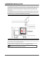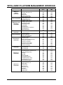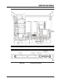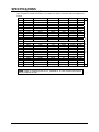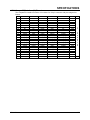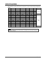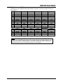
1
Technical Reference Manual
for PP 41x/03x CompactPCI®
Intel® Core Duo® Processor
Intelligent Dual PMC Carrier
Manual Order Code 560 0024 Rev 04 January 2007
Concurrent Technologies Inc
3840 Packard Road
Suite 130
Ann Arbor, MI 48108
USA
Tel: (734) 971 6309
Fax: (734) 971 6350
E-mail: [email protected]
Concurrent Technologies Plc
4 Gilberd Court
Newcomen Way
Colchester, Essex CO4 9WN
United Kingdom
Tel: (+44) 1206 752626
Fax: (+44) 1206 751116
http://www.gocct.com
NOTES
Information furnished by Concurrent Technologies is believed to be accurate and reliable.
However, Concurrent Technologies assumes no responsibility for any errors contained in this
document and makes no commitment to update or to keep current the information contained in
this document. Concurrent Technologies reserves the right to change specifications at any time
without notice.
Concurrent Technologies assumes no responsibility either for the use of this document or for any
infringements of the patent or other rights of third parties which may result from its use. In
particular, no license is either granted or implied under any patent or patent rights belonging to
Concurrent Technologies.
No part of this document may be copied or reproduced in any form or by any means without the
prior written consent of Concurrent Technologies.
All companies and product names are trademarks of their respective companies.
CONVENTIONS
Throughout this manual the following conventions will apply:
•
•
•
•
•
# or * after a name represents an active low signal. e.g. INIT* or INIT#
h denotes a hexadecimal number. e.g. FF45h
byte represents 8-bits
word represents 16-bits
dword represents 32-bits
NOTATIONAL CONVENTIONS
ii
NOTE:
Notes provide general additional information.
WARNING:
Warnings provide indication of board malfunction if they are not
observed.
CAUTION:
Cautions provide indications of board or system damage if they are not
observed.
PP 41x/03x
GLOSSARY OF TERMS
AC’97 ............................... Audio CODEC 1997
ACPI ................................ Advanced Configuration and Power Interface
APIC ................................ Advanced Programmable Interrupt Controller
ATA.................................. AT Attachment
BIOS ................................ Basic Input Output System
BMC................................. Baseboard Management Controller
CMOS .............................. Complementary Metal Oxide Semiconductor
CODEC............................ Coder / Decoder
CPCI ................................ CompactPCI
CPU ................................. Central Processing Unit
CRT ................................. Cathode Ray Tube
DDR ................................. Double Data Rate
DDR2 ............................... Double Data Rate, second generation
DIB................................... Dual Independent Bus
DIL ................................... Dual In Line
ECC ................................. Error Checking and Correcting
EIDE ................................ Enhanced Integrated Drive Electronics
EMC................................. Electromagnetic Compatibility
EPROM............................ Electrically Programmable Read Only Memory
EEPROM ......................... Electrically Erasable Programmable Read Only Memory
FRU ................................. Field Replacement Unit
FWH................................. Firmware Hub
MCH................................. Memory Controller Hub
ICH................................... I/O Controller Hub
IEEE................................. Institute of Electrical and Electronics Engineers
I/O .................................... Input/Output
IPMB ................................ Intelligent Platform Management Bus
IPMI ................................. Intelligent Platform Management Interface
LED.................................. Light Emitting Diode
LFM.................................. Linear Feet per Minute
LPC.................................. Low Pin Count
N/A................................... Not Applicable or Not Available
NC.................................... Not Connected
NMI .................................. Non Maskable Interrupt
PC-AT .............................. Personal Computer-Advanced Technology
PCI................................... Peripheral Component Interconnect
PICMG ............................. PCI Industrial Computer Manufacturers Group
PIC................................... Programmable Interrupt Controller
PIM .................................. Peripheral Interface Module
PIT ................................... Periodic Interrupt Timer
PMC................................. PCI Mezzanine Card
POST ............................... Power-on Self Test
PRST ............................... Push Button Reset
RoHS ............................... Restriction of Hazardous Substances
RST.................................. Reset
RTC ................................. Real Time Clock
RTM ................................. Rear Transition Module or Transition Module
SATA ............................... Serial ATA
SDR ................................. Sensor Data Record
SDRAM............................ Synchronous Dynamic Random Access Memory
SMBus ............................. System Management Bus
SMC................................. Satellite Management Controller
SMI .................................. System Management Interrupt
SMM ................................ System Management Mode
USB ................................. Universal Serial Bus
XMC................................. Switched Mezzanine Card
PP 41x/03x
iii
REVISION HISTORY
Revision
01
02
03
04
iv
Summary of Changes
First Release
Corrected J3 and J5 pin-out tables; changed AD PP5/001-3x
references to AD PP5/001-4xU
Changes for Rev B board; updated default positions on 3
switches: ‘PMC 2 PCI-X Enable’, ‘PMC 2 PCI Speed’ and
‘BIOS Defaults’; updated SM722 PCI Device ID
Changes for Rev C board, added E-Series details, added
Core 2 Duo support, added AD PP5/003 RTM details, various
minor corrections and clarifications.
Date
August 2006
September 2006
September 2006
January 2007
PP 41x/03x
TABLE OF CONTENTS
1
INTRODUCTION ...................................................................................... 1-1
1.1
General .....................................................................................................................................1-1
1.2
1.2.1
1.2.2
1.2.3
1.2.4
1.2.5
1.2.6
1.2.7
1.2.8
1.2.9
1.2.10
1.2.11
1.2.12
1.2.13
1.2.14
1.2.15
1.2.16
1.2.17
The PP 41x/03x - Main Features ..............................................................................................1-2
Central Processor .....................................................................................................................1-2
Cache Memories.......................................................................................................................1-2
Chipset......................................................................................................................................1-2
SDRAM .....................................................................................................................................1-3
PCI Busses ...............................................................................................................................1-3
EPROM.....................................................................................................................................1-3
CompactFlash™ ........................................................................................................................1-3
EIDE Controllers .......................................................................................................................1-3
USB...........................................................................................................................................1-3
PMC Interfaces .........................................................................................................................1-3
Ethernet Controllers ..................................................................................................................1-4
CompactPCI Interface...............................................................................................................1-4
System Management ................................................................................................................1-4
Serial Communications .............................................................................................................1-4
Graphics....................................................................................................................................1-4
Keyboard and Mouse................................................................................................................1-4
Real Time Clock (RTC).............................................................................................................1-4
1.3
1.3.1
1.3.2
1.3.3
Rear Transition Module Peripheral Functions...........................................................................1-5
AD PP5/001-4xU Peripheral Functions.....................................................................................1-5
AD PP5/002-0x Peripheral Functions .......................................................................................1-5
AD PP5/003-0x Peripheral Functions .......................................................................................1-6
1.4
Additional Board Options ..........................................................................................................1-7
1.5
Extended Temperature Options................................................................................................1-8
1.6
Compliance to RoHS 2002/95/EC ............................................................................................1-9
2
HARDWARE INSTALLATION................................................................. 2-1
2.1
General .....................................................................................................................................2-1
2.2
Unpacking and Inspection.........................................................................................................2-2
2.3
Default Jumper and Switch Settings .........................................................................................2-3
2.4
2.4.1
2.4.2
2.4.3
2.4.4
2.4.5
2.4.6
2.4.7
2.4.8
Front Panel Indicators and Controls .........................................................................................2-4
Run LED (R) Green ..................................................................................................................2-4
POST LED (P) Yellow...............................................................................................................2-4
Ethernet Speed LED (SPD) Yellow...........................................................................................2-4
Ethernet Link/Activity LED (LK/ACT) Green .............................................................................2-4
User LED (U) Red.....................................................................................................................2-4
Hot-Swap LED (HS) Blue..........................................................................................................2-4
EIDE Activity LED (I) Yellow .....................................................................................................2-4
Switch (SW) ..............................................................................................................................2-5
2.5
On-board CompactFlash Site ...................................................................................................2-6
2.6
Battery Installation/Replacement ..............................................................................................2-7
2.7
2.7.1
2.7.2
Installation of On-Board Mass Storage .....................................................................................2-8
Hard Disk Storage Kit (AD CP1/DR1).......................................................................................2-9
CompactFlash Storage Kit (AD 200/001)................................................................................2-10
2.8
Adding or Replacing DRAM Modules .....................................................................................2-11
2.9
2.9.1
Installing or Removing a PMC Module....................................................................................2-12
PMC Site 2 Bus Speed and Mode Selection ..........................................................................2-14
PP 41x/03x
v
2.10
CompactPCI Operating Mode Selection .................................................................................2-15
2.11
2.11.1
2.11.2
2.11.3
Reset Sources ........................................................................................................................2-16
CompactPCI Reset .................................................................................................................2-17
External Reset ........................................................................................................................2-18
CompactPCI Push Button Reset.............................................................................................2-19
2.12
2.12.1
2.12.2
2.12.3
2.12.4
Installation and Power-up .......................................................................................................2-20
Non Hot Swap Procedure - Installing......................................................................................2-21
Non Hot Swap Procedure - Removing....................................................................................2-21
Hot Swap Procedure - Installing .............................................................................................2-21
Hot Swap Procedure - Removing ...........................................................................................2-22
3
SOFTWARE INSTALLATION.................................................................. 3-1
3.1
Starting up for the first time.......................................................................................................3-1
3.2
Bootloading from CD-ROM .......................................................................................................3-2
3.3
Installing Microsoft® Windows® Operating Systems................................................................3-3
3.4
Installing RedHat® Linux®........................................................................................................3-4
4
MASS STORAGE INTERFACES ............................................................ 4-1
4.1
EIDE Interfaces.........................................................................................................................4-1
4.2
SATA Interfaces........................................................................................................................4-1
5
ETHERNET INTERFACES ...................................................................... 5-1
5.1
Rear Ethernet Configuration .....................................................................................................5-1
5.2
PICMG 2.16 Configuration........................................................................................................5-1
5.3
Ethernet Interface Identification ................................................................................................5-1
6
OTHER INTERFACES ............................................................................. 6-1
6.1
6.1.1
6.1.2
Serial Ports ...............................................................................................................................6-1
PC BIOS Serial Console ...........................................................................................................6-2
PC BIOS Serial Console Port ...................................................................................................6-3
6.2
Keyboard and Mouse Ports ......................................................................................................6-4
6.3
Graphics (VGA) Controller ........................................................................................................6-4
6.4
Real-Time Clock .......................................................................................................................6-4
6.5
Universal Serial Bus (USB).......................................................................................................6-4
6.6
Power On Self Test LED/Speaker ............................................................................................6-4
6.7
Audio.........................................................................................................................................6-4
7
INTELLIGENT PLATFORM MANAGEMENT INTERFACE .................... 7-1
7.1
Introduction ...............................................................................................................................7-1
7.2
IPMI Compatibility .....................................................................................................................7-2
7.3
7.3.1
7.3.2
7.3.3
7.3.4
7.3.5
IPMI Overview...........................................................................................................................7-3
Message Passing......................................................................................................................7-3
Events .......................................................................................................................................7-3
System Event Log.....................................................................................................................7-3
Sensors.....................................................................................................................................7-4
Sensor Data Records................................................................................................................7-4
vi
PP 41x/03x
7.3.6
7.3.7
Field Replaceable Unit Inventory Data .....................................................................................7-4
Watchdog..................................................................................................................................7-4
7.4
7.4.1
7.4.2
7.4.3
7.4.4
7.4.4.1
7.4.4.2
7.4.4.3
7.4.4.4
7.4.4.5
7.4.4.6
7.4.4.7
7.4.4.8
7.4.4.9
7.4.4.10
7.4.4.11
Supported Commands ..............................................................................................................7-5
Get Self Test Results Command ..............................................................................................7-7
Watchdog Commands ..............................................................................................................7-7
SEL and SDR Commands ........................................................................................................7-7
Sensor Commands ...................................................................................................................7-8
Board and CPU Temperature Sensors .....................................................................................7-9
Fan Monitor...............................................................................................................................7-9
Board Voltage Sensors .............................................................................................................7-9
CompactPCI Slot Number.........................................................................................................7-9
CompactPCI BDSEL Signal......................................................................................................7-9
CompactPCI SYSEN Signal .....................................................................................................7-9
CompactPCI PRESENT Signal.................................................................................................7-9
Hot Swap Control Power Good.................................................................................................7-9
Hot Swap Control Power Fail....................................................................................................7-9
Ejector Handle ........................................................................................................................7-10
Power Regulators Status ........................................................................................................7-10
7.5
7.5.1
7.5.2
7.5.3
7.5.3.1
7.5.3.2
7.5.3.3
7.5.3.4
7.5.3.5
7.5.3.6
7.5.3.7
FRU Inventory Data ................................................................................................................7-11
Common Header Area ............................................................................................................7-11
Board Area..............................................................................................................................7-12
Board Area Format Version ....................................................................................................7-12
Board Area Length..................................................................................................................7-12
Language Code ......................................................................................................................7-12
Manufacturing Date and Time.................................................................................................7-12
Manufacturer’s Name..............................................................................................................7-12
Board’s Name .........................................................................................................................7-12
Serial Number .........................................................................................................................7-12
FRU File ID .............................................................................................................................7-12
7.6
7.6.1
7.6.2
7.6.3
Programming Examples..........................................................................................................7-13
Using the SMIC Interface........................................................................................................7-13
Using the Watchdog Timer .....................................................................................................7-16
Reading Sensors ....................................................................................................................7-19
7.7
In System Programming .........................................................................................................7-21
8
FLASH EPROM AND DRAM................................................................... 8-1
8.1
Flash EPROM ...........................................................................................................................8-1
8.2
DRAM .......................................................................................................................................8-1
9
ADDITIONAL LOCAL I/O FUNCTIONS .................................................. 9-1
9.1
Status & Control Register 0 ......................................................................................................9-3
9.2
Status & Control Register 1 ......................................................................................................9-4
9.3
Status & Control Register 2 ......................................................................................................9-5
9.4
General Purpose I/O Register...................................................................................................9-6
9.5
CPCI Status Register................................................................................................................9-7
9.6
Interrupt Control Register..........................................................................................................9-8
9.7
9.7.1
Temperature Sensor Data Register ..........................................................................................9-9
Analogue Temperature Sensor Data Register..........................................................................9-9
9.8
ACPI PM1 Control Register ....................................................................................................9-10
9.9
Interrupt Configuration Register..............................................................................................9-11
9.10
IPMI SMIC Interface................................................................................................................9-12
PP 41x/03x
vii
9.10.1
9.10.2
9.10.3
SMIC Data Register ................................................................................................................9-12
SMIC Control/Status Register.................................................................................................9-12
SMIC Flags Register...............................................................................................................9-12
9.11
P.O.S.T. LED / Speaker..........................................................................................................9-13
9.12
PORT 80 .................................................................................................................................9-14
10
PC BIOS................................................................................................. 10-1
10.1
Entering the PC BIOS .............................................................................................................10-1
10.2
The PC BIOS Startup Sequence ............................................................................................10-3
10.3
Boot Device Selection.............................................................................................................10-4
10.4
10.4.1
10.4.2
10.4.3
10.4.4
10.4.5
10.4.6
10.4.7
10.4.7.1
10.4.7.2
10.4.8
10.4.8.1
10.4.8.2
PCI Bus Resource Management ............................................................................................10-5
PCI Express Links...................................................................................................................10-5
PCI Resource Allocation .........................................................................................................10-5
PCI Device IDs........................................................................................................................10-8
CompactPCI Bridge Configuration..........................................................................................10-9
System Controller Mode .........................................................................................................10-9
Satellite Mode .........................................................................................................................10-9
Peripheral Mode......................................................................................................................10-9
Downstream Windows ............................................................................................................10-9
Upstream Windows.................................................................................................................10-9
Peripheral Mode Window-Size Limitations ...........................................................................10-10
I/O Windows..........................................................................................................................10-10
Memory Mapped Windows ...................................................................................................10-10
10.5
User Selectable NVRAM Defaults ........................................................................................10-11
10.6
The Recovery BIOS ..............................................................................................................10-12
11
SYSTEM MANAGEMENT...................................................................... 11-1
11.1
Power Management................................................................................................................11-1
11.2
11.2.1
11.2.2
11.2.3
11.2.4
11.2.5
Thermal Management.............................................................................................................11-2
Thermal Monitor 1 (TM1) ........................................................................................................11-2
Thermal Monitor 2 (TM2) ........................................................................................................11-2
CPU Thermal Trip ...................................................................................................................11-2
PC BIOS Setup Options..........................................................................................................11-3
Processor Thermal Status Indication ......................................................................................11-3
11.3
11.3.1
11.3.2
11.3.3
11.3.4
ECC Error Logging..................................................................................................................11-4
Single-bit ECC Errors..............................................................................................................11-4
Multi-bit ECC Errors ................................................................................................................11-4
Background ECC Event Logging ............................................................................................11-4
Memory Scrubbing..................................................................................................................11-4
A
SPECIFICATIONS ...................................................................................A-1
A.1
Functional Specification ........................................................................................................... A-1
A.2
A.2.1
A.2.2
Environmental Specification (N Series) ................................................................................... A-2
Temperature Range................................................................................................................. A-2
Humidity ................................................................................................................................... A-2
A.3
Dimensions .............................................................................................................................. A-3
A.4
A.4.1
Electrical Specification ............................................................................................................. A-4
Power Supply Requirements ................................................................................................... A-4
A.5
A.5.1
Connectors............................................................................................................................... A-5
CompactPCI Interface (J1) Pin-outs ........................................................................................ A-6
viii
PP 41x/03x
A.5.2
A.5.3
A.5.4
A.5.5
A.5.6
A.5.7
A.5.8
A.5.9
A.5.10
CompactPCI Interface (J2) Pin-outs ........................................................................................ A-7
CompactPCI Interface (J3) Pin-outs ........................................................................................ A-8
CompactPCI Interface (J5) Pin-outs ........................................................................................ A-9
On-Board Mass Storage Option Connector (P5) Pin-outs ..................................................... A-10
PMC Site Connectors (J11 - J14 and J21 - J24) Pin-outs ..................................................... A-11
XMC Connector (J25) Pin-out................................................................................................ A-15
Ethernet Connector (P2) Pin-out............................................................................................ A-16
Port 80 (S1) Pin-outs ............................................................................................................. A-17
Shared Front Panel Connector (J6) Pin-outs......................................................................... A-18
PP 41x/03x
ix
TABLE OF FIGURES
x
Figure 1-1
Figure 2-1
Figure 2-2
Figure 2-3
Figure 2-4
Figure 2-5
Figure 2-6
Figure 2-7
Figure 2-8
Figure 2-9
Figure 2-10
Figure 2-11
Figure 2-12
Figure 2-13
Figure 2-14
Figure 2-15
Figure 2-16
Figure 2-17
Figure 6-1
Figure 6-2
Figure 7-1
Figure 10-1
Figure 10-2
Figure 10-3
Overview..........................................................................................................................1-1
Default Jumper and Switch Settings................................................................................2-3
Front Panel Indicators and Controls ................................................................................2-4
Front Panel Switch Function............................................................................................2-5
CompactFlash Site ..........................................................................................................2-6
Battery Fitting and CMOS Clear Jumper .........................................................................2-7
Mass Storage Connector and Fixing Holes .....................................................................2-8
Disk Drive Cable Installation............................................................................................2-9
CompactFlash Carrier Module Installation.....................................................................2-10
AD 200/001 DIL Switch Settings ...................................................................................2-10
DRAM Module Replacement .........................................................................................2-11
PMC Site 1 V(I/O) Select Jumper ..................................................................................2-12
PMC Site 2 Installation Diagram....................................................................................2-13
PMC 2 PCI Bus Speed Select and PCI-X Enable Switches..........................................2-14
Satellite Mode Switch ....................................................................................................2-15
CompactPCI Reset Input Switch ...................................................................................2-17
External Reset Switch....................................................................................................2-18
CompactPCI Push Button Reset Switch........................................................................2-19
Console Switch ................................................................................................................6-2
Console Port Switch ........................................................................................................6-3
Firmware Mode Switch ..................................................................................................7-21
Boot Mode Switch..........................................................................................................10-1
BIOS Defaults Switch ..................................................................................................10-11
Boot Type Switch.........................................................................................................10-12
Figure A-1
Figure A-2
Figure A-3
Connector Layout ........................................................................................................... A-5
Front Panel Connectors.................................................................................................. A-5
Shared Front Panel Connector Layout ......................................................................... A-18
PP 41x/03x
TABLE OF TABLES
Table 2-1
Table 5-1
Table 6-1
Table 7-1
Table 7-2
Table 7-3
Table 7-4
Table 9-1
Table 10-1
Table 10-2
Table 11-1
Reset Configuration Options..........................................................................................2-16
Ethernet Interface Identification .......................................................................................5-1
Serial Port Numbering .....................................................................................................6-1
Supported IPMI Commands ............................................................................................7-6
Sensor ID Codes .............................................................................................................7-8
FRU Inventory Area : Common Header Area Data .......................................................7-11
FRU Inventory Area : Board Area Data .........................................................................7-12
I/O Address Map..............................................................................................................9-1
PCI Device Interrupt Allocations ....................................................................................10-6
PCI Device Numbers .....................................................................................................10-8
CPU Operating Speed BIOS Options ............................................................................11-1
Table A-1
Table A-2
Table A-3
Table A-4
Table A-5
Table A-6
Table A-7
Table A-8
Table A-9
Table A-10
Table A-11
Table A-12
Table A-13
Table A-14
Voltage and Current Requirements ................................................................................ A-4
CompactPCI J1 Interface Pin-outs ................................................................................. A-6
CompactPCI J2 Interface Pin-outs ................................................................................. A-7
CompactPCI J3 Interface Pin-outs ................................................................................. A-8
CompactPCI J5 Interface Pin-outs ................................................................................. A-9
On-Board Mass Storage Option (P5) Interface Pin-outs .............................................. A-10
PMC J11 and J21 Connector Pin-outs ......................................................................... A-11
PMC J12 and J22 Connector Pin-outs ......................................................................... A-12
PMC J13 and J23 Connector Pin-outs ......................................................................... A-13
PMC J14 and J24 Connector Pin-outs ......................................................................... A-14
XMC J25 Connector Pin-outs ....................................................................................... A-15
Ethernet RJ-45 P2 Connector Pin-outs ........................................................................ A-16
Port 80 S1 Connector Pin-outs ..................................................................................... A-17
Shared Front Panel Connector (J6) Pin-outs................................................................ A-18
PP 41x/03x
xi
This page has been left intentionally blank
xii
PP 41x/03x
1
1.1
INTRODUCTION
General
This manual is a guide and reference handbook for engineers and system integrators who wish to
use the Concurrent Technologies’ PP 41x/03x ultra high-performance Intel® Core™ Duo or Intel®
Core™ 2 Duo processor single board computer. The board has been designed for high-speed
multiprocessing applications using a PC-AT™ architecture operating in a CompactPCI Bus
environment.
The PP 41x/03x board is available in several different variants which differ by the processor speed,
the amount of fitted SDRAM and the rear Ethernet connector configuration. Currently the board is
available with a 1.66 GHz Intel® Low Voltage Core Duo® processor L2400, a 2.0 GHz Intel® Core
Duo® processor T2500 or a 2.16GHz Intel® Core 2 Duo® processor T7400. These models are
designated PP 410/031, PP 410/032 and PP 412/032 respectively. The other configuration options
are specified by a two-digit suffix to the board name; refer to the product data sheet for further
details. Further details of other board options are given in Section 1.3. References to the board in
this document will use the name PP 41x/03x unless they apply only to a specific variant, in which
case the full name will be used.
The information contained in this manual has been written to provide users with all the information
necessary to configure, install and use the PP 41x/03x as part of a system. It assumes that the
user is familiar with the CompactPCI bus and PC-AT bus architectures and features.
Figure 1-1
PP 41x/03x
Overview
1-1
INTRODUCTION
1.2
The PP 41x/03x - Main Features
The PP 41x/03x is a member of the Concurrent Technologies range of single-board computers for
the CompactPCI bus architecture. It has been designed as a powerful single board computer
based upon the Intel Core Duo or the Intel Core 2 Duo processor, the Intel® E7520 and 6300ESB
chipset and three Intel® 82573L Gigabit Ethernet controllers. It also provides two IEEE 1386.1
PMC sites (one of which also supports XMC), optional on-board mass storage, and interfaces for
standard PC-AT based peripherals.
1.2.1 Central Processor
The central processor used on this board is either an Intel Core Duo processor, operating internally
at 1.66 GHz or 2.0 GHz or an Intel Core 2 Duo processor, operating internally at 2.16 GHz.
Both processor types have two high performance execution cores. Those in the Core Duo
processor are derived from the Intel Pentium M processor, whereas those in the Core 2 Duo
processor are based on the latest Intel Core architecture. The 64-bit frontside bus is connected to
the memory controller at 667 MHz to provide a maximum transfer bandwidth of 5.3 Gbytes/s. The
processor is capable of addressing 4 Gbytes of physical memory all of which is cacheable, and 64
Terabytes of virtual memory.
The Intel Core Duo and Core 2 Duo processors are upwardly code-compatible with the other
members of the x86 family of microprocessors. They have in-built floating point coprocessors for
compatibility with 486 and 386/387 designs. The Core 2 Duo processor also supports Intel 64
architecture (i.e. 64-bit operation).
Elsewhere in this manual the processor is referenced as the Intel Core Duo processor regardless
of the exact CPU chip being used.
1.2.2 Cache Memories
The Level 1 and Level 2 caches are both implemented on the processor die for maximum
performance. Each of the two execution cores has its own Level 1 cache and they share a
common Level 2 cache. The Level 1 cache is organized as 32 Kbytes of instruction cache and 32
Kbytes of data cache. The Level 2 cache stores both instructions and data. It operates at the core
frequency and is based on Intel’s Advanced Transfer Cache architecture. The Core Duo processor
has 2 Mbytes of Level 2 cache, whereas the Core 2 Duo processor has 4 Mbytes of Level 2 cache.
1.2.3 Chipset
The PP 41x/03x uses the Intel E7520 and 6300ESB chipset. This is comprised of the E7520
Memory Controller Hub (MCH) and the 6300ESB I/O Controller Hub (ICH). They respectively
provide North Bridge + PCI Express controller and South Bridge + PCI bus controller functionality.
The E7520 MCH interfaces to the CPU’s host bus. It provides a dual-channel DDR2 SDRAM
memory controller, three configurable PCI Express links and a high speed Hub Interface 1.5 which
connects to the 6300ESB ICH. It supports concurrent CPU, memory, PCI Express and Hub
Interface bus operations.
The 6300ESB ICH provides a 66 MHz 64-bit PCI or PCI-X bus for supporting high performance
PCI devices. It also provides a 33 MHz 32-bit PCI bus. The Hub Interface supports a maximum
transfer bandwidth of 266 Mbytes/s.
The 6300ESB ICH also provides a variety of peripheral functions including Serial ATA (SATA)
controllers, EIDE controllers, USB 2.0 and 1.1 controllers, LPC (Low Pin Count) Bus bridge,
IOAPIC interrupt controller, Real Time clock (RTC), two serial ports and other legacy PC-AT
architectural functions.
The LPC Bus is used to connect to the Firmware Hub (FWH), the control and status registers and
to the PC87391 Super I/O Controller on the companion AD PP5/001-4xU Transition Module. This
device implements a floppy disk controller, a parallel port and two additional serial ports.
1-2
PP 41x/03x
INTRODUCTION
1.2.4 SDRAM
The SDRAM controller within the E7520 MCH supports dual DDR2 400MHz memory channels with
ECC data protection. These provide a maximum memory transfer bandwidth of 6.4 Gbytes/s. The
memory is implemented with DDR2 Registered ECC SODIMM modules. Two 200-pin SODIMM
sockets are provided, one per channel. The board will accept modules having a capacity up to 2
Gbytes each. Hence a maximum of 4 Gbytes of memory may be fitted to the board.
1.2.5 PCI Busses
The 6300ESB ICH provides two of the on-board PCI busses. The primary bus is 64-bits wide and
provides a high performance, up to 528 Mbytes/s, connection between the 6300ESB ICH and PMC
site 1. The secondary PCI bus is 32-bits wide and provides a lower performance, up to 132
Mbytes/s, connection between the 6300ESB ICH and a Silicon Motion SM722 Graphics controller.
A PLX Technology PEX8114 PCI Express to PCI-X bridge provides a third, very high performance
64-bit PCI / PCI-X bus. This bus can operate in PCI mode at either 33 MHz or 66 MHz, or in PCI-X
mode at 100 MHz and offers a bandwidth of up to 800 Mbytes/s. This bus connects to PMC site 2
and a PLX Technology PCI6540 PCI-X to PCI bridge. The latter implements the CompactPCI
backplane interface. The PEX8114 is connected to the E7520 MCH by a 4-lane PCI Express link,
which offers a bandwidth of up to 1 Gbyte/s in each direction.
1.2.6 EPROM
The board contains a 1 Mbyte Firmware Hub (FWH) for the BIOS code and fixed data and factory
test software.
1.2.7 CompactFlash™
The PP 41x/03x contains an on-board CompactFlash site, which is located below PMC site 1. The
CompactFlash site primarily supports Type 1 modules. Type 2 modules may be fitted subject to
them not interfering mechanically with the PMC module. CompactFlash provides a flexible and
cost-effective alternative to on-board Flash memory for application program and data storage.
1.2.8 EIDE Controllers
The PP 41x/03x has two EIDE/Ultra ATA100 interfaces. The CompactFlash site uses the
secondary EIDE interface. The primary EIDE interface is available via an on-board connector for
use by the optional on-board disk drive or dual CompactFlash carrier.
1.2.9 USB
The PP 41x/03x provides four USB channels, one via the front panel shared console connector and
three via the CompactPCI J5 connector. All four USB channels support both USB 1.1 (1.5 Mbit/s
and 12 Mbits/s) and USB 2.0 (480 Mbits/s) operation.
1.2.10 PMC Interfaces
Two PMC interfaces, which support single width 64 or 32-bit PMC modules complying with the
IEEE 1361.1 standard, are provided.
PMC site 1 will operate at either 33 MHz or 66 MHz and supports both 3.3V and 5V PCI signaling.
PMC site 2 will operate at either 33 MHz or 66 MHz in PCI mode or at 100 MHz in PCI-X mode. It
supports only 3.3V signaling. PMC site 2 also provides an XMC connector. This connector has an
8-lane PCI Express link to the E7520 MCH, which offers a bandwidth of up to 2 Gbytes/s in each
direction.
The PMC interfaces will also accept dual function and Processor PMC modules. The latter will
operate only in non-Monarch mode.
PP 41x/03x
1-3
INTRODUCTION
1.2.11 Ethernet Controllers
Three Intel® 82573L Gigabit Ethernet controller are used to provide high performance PCI Express
to Ethernet interfaces. All three channels support 10, 100 and 1000 Mbits/s operation. One
channel is routed to a front panel RJ45 connector; the other two channels are routed to the
CompactPCI J3 connector.
The board can either support PICMG® 2.16 backplane networking or rear panel Ethernet. This is
specified by an ordering option. A suitable Transition Module, such as the AD PP5/002-00, is
required for rear panel Ethernet.
1.2.12 CompactPCI Interface
The PP 41x/03x is a CompactPCI compatible System Controller board. It may also act as a
Peripheral board or as a Satellite board in any backplane slot. The board uses a 64-bit interface
implemented with a PLX Technology PCI6540 PCI-X to PCI bridge. As a System Controller it
supports PICMG 2.1 compliant Hot Swap Peripheral Boards. As a Peripheral board it may be Hot
Swapped under the control of the System Controller. As a Satellite board it may be Hot Swapped
under the control of an on-board microcontroller.
1.2.13 System Management
The PP 41x/03x supports PICMG 2.9 system management. The IPMI SMIC interface is
implemented and the CompactPCI IPMB 0 and IPMB 1 communication channels are provided. An
on-board microcontroller provides the requisite IPMI functionality. The microcontroller can be
configured to provide Baseboard Management Controller (BMC) functionality.
1.2.14 Serial Communications
The PP 41x/03x provides two RS232 serial data communication port. These are implemented by
the 6300ESB ICH. The COM1 serial interface is available via the front panel shared console
connector. Sufficient modem control signals are provided to support serial console operation or file
transfers, namely TxD, RxD, RTS and CTS.
The COM2 serial interface is available via the CompactPCI J5 connector. The full set of modem
control signals are provided.
A splitter cable, part number CB 26D/125-00, is required to access the interfaces on the front panel
shared console connector.
1.2.15 Graphics
The PP 41x/03x provides analog SVGA graphics using a Silicon Motion SM722 graphics controller.
This device contains 8 Mbytes of local RAM and offers resolutions up to 1280 x 1024 with 32-bit
color support. The SVGA interface is accessed via the front panel shared console connector.
A splitter cable, part number CB 26D/125-00, is required to access the interfaces on the front panel
shared console connector.
1.2.16 Keyboard and Mouse
The PP 41x/03x supports PS/2™ type keyboard and mouse interfaces. These are accessed via the
front panel shared console connector.
USB keyboard and mouse are also supported. These devices may either be connected to the USB
ports on the Transition Module, or be connected, via a USB hub, to the front panel shared console
connector.
A splitter cable, part number CB 26D/125-00, is required to access the interfaces on the front panel
shared console connector.
1.2.17 Real Time Clock (RTC)
A battery backed RTC device provides PC-AT clock, calendar and configuration RAM functions.
The RTC and BIOS are year 2000 compliant.
1-4
PP 41x/03x
INTRODUCTION
1.3
Rear Transition Module Peripheral Functions
Three Rear Transition Modules (RTMs) may be used with the PP 41x/03x board, namely the
AD PP5/001-4xU, the AD PP5/002-0x and the AD PP5/003-0x. Each of these RTMs provides a
different set of peripheral functions.
1.3.1 AD PP5/001-4xU Peripheral Functions
The AD PP5/001-0x (or AD PP5/001-0xU) RTM was originally designed for use with the
PP 31x/01x family of boards. It has been modified for operation with the PP 41x/03x and in this
form becomes the AD PP5/001-4xU. However, it may be used with the PP 41x/03x subject to some
limitations, discussed below. The main feature of the AD PP5/001-4xU is that it contains a
PC87391 Super I/O controller. This device provides the following interfaces:
•
•
•
Floppy disk interface for up to two floppy disk drives.
Parallel port interface.
Two RS232 serial interfaces.
The AD PP5/001-4xU also provides:
•
•
•
•
•
•
•
•
•
•
68-pin connector for PMC site 1 rear I/O.
68-pin connector for PMC site 2 rear I/O.
68-pin in-board connector for PMC site 2 SCSI.
Two Gigabit Ethernet ports.
One USB port.
Two general purpose inputs.
Two general purpose outputs.
External Reset input.
Fan sensor input.
PC speaker output.
The AD PP5/001-4xU does not support the SATA, Audio and two of the USB interfaces of the
PP 41x/03x.
CAUTION: The Compact Flash and 1.8 inch hard disk drive EIDE interfaces on the
AD PP5/001-0x and AD PP5/001-3x (or AD PP5/001-0xU and AD PP5/001-3xU) are not
supported by the PP 41x/03x, even though many functions are common to all these
variants. Do not connect cables to the unsupported EIDE interfaces when using these
Transition Modules with the PP 41x/03x.
1.3.2 AD PP5/002-0x Peripheral Functions
The AD PP5/002-0x RTM is specifically designed for use with the PP 41x/03x. It provides the
following interfaces:
•
•
•
•
•
•
•
•
•
•
•
•
PP 41x/03x
68-pin connector for PMC site 1 rear I/O.
68-pin connector plus 68-pin in-board connector for PMC site 2 rear I/O.
68-pin in-board connector for PMC site 2 SCSI.
Two Serial ATA (SATA) interfaces.
Two Gigabit Ethernet ports.
Two USB ports.
One RS232 serial interface (COM2).
AC97 audio with in-board jack sockets for microphone, line input, line output and headphones.
Two general purpose inputs.
Two general purpose outputs.
External Reset input.
Fan sensor input.
1-5
INTRODUCTION
1.3.3 AD PP5/003-0x Peripheral Functions
The AD PP5/003-0x RTM provides flexible PMC site rear I/O management by the use of Peripheral
Interface Modules (PIMs). It provides the following interfaces:
•
•
•
•
•
•
•
•
•
•
•
•
1-6
PIM site for PMC site 1 rear I/O.
PIM site for PMC site 2 rear I/O.
68-pin in-board connector for PMC site 2 SCSI.
Two Serial ATA (SATA) interfaces.
One Gigabit Ethernet port.
Two USB ports.
One RS232 serial interface (COM2).
AC’97 audio with in-board header for microphone, line input, line output and headphones.
Two general purpose inputs.
Two general purpose outputs.
External Reset input.
Fan sensor input.
PP 41x/03x
INTRODUCTION
1.4
Additional Board Options
The PP 41x/03x board may be ordered with one of a few factory fitted configuration options, in
particular the Ethernet (on J3 connector):
•
•
Configured for PICMG 2.16 backplane networking
Configured for rear panel Ethernet via connectors (on RTM)
Two mezzanine mass storage options are available, namely:
•
•
A 2.5 inch EIDE hard disk drive of at least 20 Gbyte capacity
A dual CompactFlash carrier that also supports the Hitachi GST MicroDrive™
Refer to the PP 41x/03x datasheet for ordering information. The datasheet also details the
SDRAM capacity options.
NOTE: The mezzanine mass storage options use the PMC site 1 area. No PMC module
may be fitted in this site when a mezzanine mass storage option is fitted. PMC site 2 is
not affected by fitting a mezzanine mass storage option.
A bottom side cover is available. This protects the components on the bottom side of the board
from accidental damage or short circuits, particularly during hot-swap insertion and removal.
PP 41x/03x
1-7
INTRODUCTION
1.5
Extended Temperature Options
All variants of the board are qualified for the standard operating and storage temperature ranges
indicated in Section A.2.1. Some variants of the board are available which offer a wider range of
operating and storage temperatures, but certain board features are no longer available with these
variants. In particular the option for on-board mass storage using a 2.5 inch hard disk drive is not
supported for the extended temperature specifications.
Consult your distributor or Concurrent Technologies directly for details of the extended temperature
options.
NOTE: A bottom side cover should not be fitted if the operating ambient temperature will
exceed 55°C. This restriction is necessary to prevent overheating of some devices on the
bottom side of the board.
1-8
PP 41x/03x
INTRODUCTION
1.6
Compliance to RoHS 2002/95/EC
This product is offered in a form which complies to the RoHS 2002/95/EC
directive. The European Union RoHS 2002/95/EC directive restricts the use
of six materials in electronic components and assemblies. Specifically, these
materials are Lead (Pb), Mercury (Hg), Cadmium (Cd), Hexavalent
Chromium (Cr VI), Polybrominated Biphenyls (PBB) and Polybrominated
Diphenyl Ethers (PBDE). Concurrent Technologies is committed to
compliance to the RoHS directive.
Some components on these boards use packaging which is not lead-free, but which complies with
RoHS regulations as a result of technology-specific exemptions.
PP 41x/03x
1-9
INTRODUCTION
This page has been left intentionally blank
1-10
PP 41x/03x
2
2.1
HARDWARE INSTALLATION
General
This chapter contains general information on unpacking and inspecting the PP 41x/03x after
shipment, and information on how to configure board options and install the board into a
CompactPCI chassis.
CAUTION: It is strongly advised that, when handling the PP 41x/03x and its associated
components, the user should at all times wear an earthing strap to prevent damage to the
board as a result of electrostatic discharge.
CAUTION: The heatsink used on the 2.0 GHz or 2.16 GHz processor variants of this
board will be hot during and after use. Care should be taken when handling the board.
The list below outlines the steps necessary to configure and install the board. Each entry in the list
refers to a section in this chapter which will provide more details of that stage of the procedure. It
is recommended that the board is configured in the sequence below.
1) Unpack the board - see Section 2.2.
2) Locate and familiarize yourself with the front panel indicators and controls - see
Section 2.4.
3) Check that the board jumper settings match the required operating mode. See Section
2.3 for details of the default settings and where to find more information.
4) Fit a Compact Flash module if required - see Sections 2.5 and 2.7.
5) Fit the battery if necessary - see Section 2.6.
6) Fit a Mass Storage Module if required – see Section 2.7.
7) Change or fit DRAM SODIMMs if required – see Section 2.8.
8) Fit the PMC modules(s) if required - see Section 2.9.
9) Configure the board for the correct CompactPCI operating mode and for any external
sources for board or system resets - see Sections 2.10 and 2.11.
10) Install the board, using Hot Swap or non-Hot Swap procedures - see Section 2.12.
PP 41x/03x
2-1
HARDWARE INSTALLATION
2.2
Unpacking and Inspection
Immediately after the board is delivered to the user’s premises the user should carry out a thorough
inspection of the package for any damage caused by negligent handling in transit.
CAUTION: If the packaging is badly damaged or water-stained the user must insist on
the carrier’s agent being present when the board is unpacked.
Once unpacked, the board should be inspected carefully for physical damage, loose components
etc. In the event of the board arriving at the customer’s premises in an obviously damaged
condition Concurrent Technologies or its authorized agent should be notified immediately.
2-2
PP 41x/03x
HARDWARE INSTALLATION
2.3
Default Jumper and Switch Settings
Figure 2-1
PP 41x/03x
Default Jumper and Switch Settings
2-3
HARDWARE INSTALLATION
2.4
Front Panel Indicators and Controls
When installing or removing the board for the first time, or when checking its operation, it can be
very useful to note the behavior of the LEDs on the front panel. Figure 2-2 shows the location of
the LEDs, and their purpose is outlined below.
Figure 2-2
Front Panel Indicators and Controls
2.4.1 Run LED (R) Green
The run LED indicates that activity is occurring on the LPC bus or the 32-bit PCI bus. This allows
the user to quickly assess how active the busses are.
2.4.2 POST LED (P) Yellow
The POST LED is used to indicate that a power on self test has failed. This LED will also flash
when outputting sound on the speaker.
2.4.3 Ethernet Speed LED (SPD) Yellow
This LED indicates the operating speed of the front panel Ethernet interface, as follows:
•
•
•
Off = 10Mbits/s
Steady On = 100Mbits/s
Flashing = 1000Mbits/s
2.4.4 Ethernet Link/Activity LED (LK/ACT) Green
This LED lights when connection has been made on the front panel Ethernet interface. It will flash
to indicate link activity, and during periods of high Ethernet activity the LED may switch off for
several seconds.
2.4.5 User LED (U) Red
This LED is available for use by user software. It is manipulated via an I/O register (see Section
9.2 for details). Alternatively, the User LED may be configured to light when the CPU reaches its
maximum specified operating temperature (see Section 11.2.3). In either mode, the User LED will
flash rapidly if the CPU Thermal Trip activates (see Section 11.2.6).
2.4.6 Hot-Swap LED (HS) Blue
This LED is used when the board is hot-swapped, and lights to indicate when the board can be
safely removed from the chassis.
2.4.7 EIDE Activity LED (I) Yellow
This LED lights when there is activity on the on-board EIDE interfaces or the SATA interfaces.
2-4
PP 41x/03x
HARDWARE INSTALLATION
2.4.8 Switch (SW)
A pushbutton switch is recessed behind the front panel, and provides a means of generating a
reset or NMI to the board.
The reset or NMI function is selected by the setting of the Front Panel Switch Function switch
shown in Figure 2-3.
Figure 2-3
Front Panel Switch Function
Selecting the Reset position setting will cause the board to be reset when the front panel switch is
operated. If the board is in the System Controller Slot, it will also assert RST# on the CompactPCI
backplane and hence will reset the other boards in the chassis. If the board is operating as a
Peripheral or Satellite, it will respond to front panel resets but will not reset the other boards in the
chassis.
Selecting the NMI position setting configures the switch to generate NMI when operated. No reset
is generated in this case.
PP 41x/03x
2-5
HARDWARE INSTALLATION
2.5
On-board CompactFlash Site
A CompactFlash site is provided on the PP 41x/03x board. The site fully supports Type I modules.
A Type II module or a MicroDrive may be fitted, but the user should be aware that these are 5.0mm
tall and therefore encroach into the clearance zone between the PP 41x/03x board and PMC
module. This may cause an interference problem if the PMC module also encroaches into this
clearance zone.
The CompactFlash site is located under PMC site 1 as shown in Figure 2-4 below. The site faces
the top edge of the board, hence the board must be removed from the chassis in order to insert or
remove the module. To fit a module, orient it such that the connector end is facing the socket and
the label side is away from the board, and gently slide it into the socket.
Figure 2-4
CompactFlash Site
The module will normally be adequately retained by the card edge guide of the chassis. However,
holes are provided for the supplied retaining strap.
To fit the strap, place it over the module, insert the two screws supplied with the strap from the
bottom side of the board and tighten the screws. Do not over tighten the screws.
NOTE: If the board is likely to be subject to mechanical vibration a suitable thread lock
compound applied to the screws should be considered.
2-6
PP 41x/03x
HARDWARE INSTALLATION
2.6
Battery Installation/Replacement
The on-board Real-Time Clock and CMOS memory used by the PC BIOS firmware are powered by
a 3.3V Lithium battery when the board is powered OFF. It is advisable, for the battery to be fitted
prior to using the board. Figure 2-5 shows how to do this. One battery is supplied with the board,
but it is not normally fitted.
If the board is operated without a battery, the User Selectable NVRAM Defaults feature can be
used to override the factory default NVRAM settings. See Section 10.5 for further details.
Figure 2-5
Battery Fitting and CMOS Clear Jumper
The battery should be replaced when the voltage falls below 2.8V. Depending on the way in which
the board is operated and stored, battery life should be in excess of 5 years. The life expectancy
will fall if the battery is subjected to long periods at temperatures of 45°C or above. It will also fall if
the battery is fitted to a board that is stored in its conductive bag even at room temperature.
CAUTION: When replacing the battery, proper anti-static precautions must be observed.
WARNING: Dispose of battery properly. DO NOT BURN. The date and time settings will
need to be initialized if the battery is disconnected.
If the BIOS setup screens have been used to set up the board for an invalid configuration, or in
other fault conditions, it may be useful to be able to reset the contents of the CMOS RAM and
Real-Time Clock. In this case, the CMOS Clear Jumper can be used.
To clear the CMOS RAM to a known state, fit the CMOS Clear jumper and apply power. When the
board is next powered down remove the jumper, otherwise CMOS RAM will again be reset.
PP 41x/03x
2-7
HARDWARE INSTALLATION
2.7
Installation of On-Board Mass Storage
If an on-board mass storage option has been ordered, it will be necessary to install the option at
this time.
The mass storage option plugs into connector P5 and is secured via screws and spacers using the
four mounting holes as shown in Figure 2-6 below.
Figure 2-6
2-8
Mass Storage Connector and Fixing Holes
PP 41x/03x
HARDWARE INSTALLATION
2.7.1 Hard Disk Storage Kit (AD CP1/DR1)
The option kit comprises:
•
•
•
•
A 2.5 inch EIDE disk drive
A ribbon cable assembly
Four M3 x 10mm screws
Four M3 x 5mm spacers
The ribbon cable assembly has a 50-way connector at one end and a 44-way connector at the
other end. The 50-way connector plugs into the disk drive and the 44-way plugs into P5 on the
PP 41x/03x.
1) Plug the 50-way connector into the disk drive as shown in Figure 2-7 below, note the
orientation.
50-way Connector
Stripe
44-way Connector
Pin 1
P5
Figure 2-7
Disk Drive Cable Installation
2) Plug the 44-way connector into P5, note the orientation.
3) Fix the disk drive into position using the four screws and spacers provided. Do not over
tighten the screws.
NOTE: If the board is likely to be subjected to mechanical vibration a suitable thread lock
compound applied to the screws should be considered.
PP 41x/03x
2-9
HARDWARE INSTALLATION
2.7.2 CompactFlash Storage Kit (AD 200/001)
The option kit comprises:
•
•
A CompactFlash carrier module with attached ribbon cable
Four M3 panhead screws
CompactFlash Carrier Module
CompactFlash Sites
Site 2
Site 1
Pillars
P5 Connector
Figure 2-8
CompactFlash Carrier Module Installation
To install the CompactFlash carrier module, follow these instructions:
1) The M3 panhead screws may be loosely screwed into the end of the pillars, if so unscrew
them.
NOTE: Do not unscrew the countersunk screws attaching the pillars to the circuit board.
2) Fix the module into position using the four panhead screws referred to earlier. Do not
over tighten the screws.
NOTE: If the board is likely to be subjected to mechanical vibration a suitable thread lock
compound applied to the screws should be considered.
3) Connect the captive ribbon cable connector to P5 on the PP 41x/03x board.
The CompactFlash sites are labeled CompactFlash 1 and CompactFlash 2.
If a single CompactFlash card is fitted, it should always be installed into site 1. Site 2 should be
used only when two CompactFlash cards are fitted.
The CompactFlash card(s) may be retained in position by fitting short M3 screws and spacers into
the holes near the long edge of the carrier. This will protect against accidental removal due to
vibration or deliberate but unauthorized removal.
NOTE: If more than one CompactFlash module is fitted, the module in the CompactFlash
2 site must support operation as a Slave device.
The DIL switch on the AD 200/001 should be set as shown in Figure 2-9.
ON
Figure 2-9
2-10
4
3
2
1
OFF
AD 200/001 DIL Switch Settings
PP 41x/03x
HARDWARE INSTALLATION
2.8
Adding or Replacing DRAM Modules
The PP 41x/03x accepts standard 200-pin DDR2-400 Registered ECC SODIMM modules
populated with 1.8V PC3200 DDR2 SDRAM. Two sockets are provided and will accommodate
modules up to 2 Gbytes capacity each. Identical SODIMMs must be fitted in both sockets. Consult
your distributor or Concurrent Technologies directly for details of suitable SODIMMs.
CAUTION: The PP 41x/03x does not support 64-bit non-ECC DDR2 SODIMM modules.
Do not fit such modules otherwise damage to the board and/or modules could result.
Figure 2-10 shows the way in which SODIMMs are fitted or removed. No other changes are
necessary when a SODIMM is added or removed.
Figure 2-10
PP 41x/03x
DRAM Module Replacement
2-11
HARDWARE INSTALLATION
2.9
Installing or Removing a PMC Module
The PP 41x/03x board provides jumper selectable 3.3V or 5V V(I/O) to PMC site 1 and fixed 3.3V
V(I/O) to PMC site 2. Before installing a PMC module check that its V(I/O) requirements match
those of the site.
CAUTION: Do not fit PMC modules designed for 5V V(I/O) only in PMC site 2. Doing so
may cause damage to the module or the PP 41x/03x.
NOTE: The PP 41x/03x board is supplied with PMC blanking plates which must be
removed before a new module can be fitted.
Figure 2-11
2-12
PMC Site 1 V(I/O) Select Jumper
PP 41x/03x
HARDWARE INSTALLATION
Figure 2-12
PP 41x/03x
PMC Site 2 Installation Diagram
2-13
HARDWARE INSTALLATION
2.9.1 PMC Site 2 Bus Speed and Mode Selection
The PCI bus connecting to PMC Site 2 can operate at various bus speeds and modes, namely, 33
MHz PCI, 66 MHz PCI, 66 MHz PCI-X and 100 MHz PCI-X. The bus speed and mode is
determined by the settings of two option switches. These switches are shown in Figure 2-13.
Switch 1 should normally be in the ON position. This forces the bus to operate in PCI mode. If a
PCI-X capable PMC module is fitted, Switch 1 should be set to the OFF position. This will allow the
bus to operate in PCI-X mode.
Switch 4 sets the speed range of the bus. If Switch 4 is OFF this will be an even multiple of 25
MHz. If Switch 4 is ON this will be an even multiple of 33 MHz.
Switch 4 should normally be in the ON position. If a 100 MHz PCI-X PMC module is fitted, Switch 4
should be set to the OFF position.
WARNING: The PP 41x/03x cannot automatically determine the speed capability of a
PCI-X capable PMC module. Switch 4 must be set correctly. If you are unsure of the
speed capability of your PMC module, set Switch 4 to the ON position.
WARNING: Do not operate the PP 41x/03x board with Switch 1 OFF, Switch 4 ON and
no PMC module fitted.
Figure 2-13
2-14
PMC 2 PCI Bus Speed Select and PCI-X Enable Switches
PP 41x/03x
HARDWARE INSTALLATION
2.10 CompactPCI Operating Mode Selection
This is normally automatic and depends only on what type of slot the board is installed into, as
detailed below:
Slot
System Controller
Bussed Peripheral
Non-Bussed Peripheral
Mode
System Controller
Peripheral or Satellite
Satellite
A switch is provided to force Satellite mode operation in any slot. The settings are shown in
Figure 2-14. In Satellite mode the board cannot communicate on the CompactPCI bus.
Figure 2-14
PP 41x/03x
Satellite Mode Switch
2-15
HARDWARE INSTALLATION
2.11 Reset Sources
In addition to the front panel switch described in Section 2.4.8, the board may be reset from several
external sources, as described below. Table 2-1 outlines how board and system resets can be
achieved using the available jumper options.
Mode
System
Controller
Peripheral
Satellite
Board Level Reset Sources
System Reset Sources
Front Panel Switch
Front Panel Switch
CompactPCI Push Button Reset CompactPCI Push Button Reset
External Reset
External Reset
Front Panel Switch
No option
CompactPCI RST# signal
External Reset
Front Panel Switch
No option
External Reset
CompactPCI RST# signal
(optional)
Table 2-1 Reset Configuration Options
Section
2.4.8
2.11.3
2.11.2
2.4.8
2.11.1
2.11.2
2.4.8
2.11.2
2.11.1
NOTE: Resets generated by hardware or software which cause a local PCI bus reset will
also activate the CompactPCI backplane reset if the board is the System Controller.
2-16
PP 41x/03x
HARDWARE INSTALLATION
2.11.1 CompactPCI Reset
The CompactPCI Reset signal is generated by the System Controller and is routed to all bussed
Peripheral slots.
If the board is in Satellite mode, it may be preferable for it to ignore the CompactPCI Reset signal.
A switch is provided to facilitate this choice. The settings are shown in Figure 2-15.
Figure 2-15
PP 41x/03x
CompactPCI Reset Input Switch
2-17
HARDWARE INSTALLATION
2.11.2 External Reset
When the PP 41x/03x board is used with an AD PP5/001-4xU, AD PP5/002-xx or AD PP5/003-xx
Rear Transition Module, a local (board-level) reset may be generated from a connector on the RTM
(see that board’s Technical Reference Manual for details). The action of that connector input is
controlled on the PP 41x/03x by the External Reset switch shown in Figure 2-16. This switch has
no function when the PP 41x/03x is used without an RTM.
Figure 2-16
External Reset Switch
NOTE: Unlike the CompactPCI Push Button Reset, this facility is available when the
board is installed in any slot.
2-18
PP 41x/03x
HARDWARE INSTALLATION
2.11.3 CompactPCI Push Button Reset
The Push Button Reset signal available on the J2 connector (PRST#) will cause a board reset if the
board is in the System Controller slot. This input can be driven from an open collector TTL output
(or discrete transistor) or normally open switch/relay contacts. To initiate the reset pull this input to
0V. This input is filtered and protected from overshoots/undershoots so no external contact
debouncing is required.
This signal is not wired to Peripheral or Satellite slots.
A switch determines whether or not assertion of this signal will reset the board. The settings are
shown in Figure 2-17.
Figure 2-17
PP 41x/03x
CompactPCI Push Button Reset Switch
2-19
HARDWARE INSTALLATION
2.12 Installation and Power-up
Before the board is installed in a CompactPCI chassis, check the following points:
•
The backplane V(I/O) configuration. The PP 41x/03x board supports either 5V or 3.3V V(I/O)
automatically. Some CompactPCI backplanes are pre-wired for a particular voltage and others
can be configured by the user. For 66 MHz CompactPCI operation the voltage must be 3.3V.
WARNING: V(I/O) must be wired on the backplane. If it is not wired the board will lock up
during POST.
•
•
•
The Power Supply Unit current capabilities. The board draws current primarily from the +5V
and 3.3V rails, and the details are provided in Section A.4.
Front panel keys. PICMG 2.10 describes a method of keying CompactPCI board front panels
to individual chassis slots. Keying pins for this purpose are supplied with the board but are not
fitted. The user is referred to PICMG 2.10 for information on using these keys.
Rear Transition Module Configuration. The AD PP5/001-4xU, AD PP5/002-0x and
AD PP5/003-0x Rear Transition Modules are intended for use with the PP 41x/03x board, and
have switch options to configure them for rear panel Ethernet or PICMG 2.16. Refer to the
appropriate Transition Module’s Technical Reference manual for further details.
The board can be installed as a System Controller in the System slot or as a Peripheral or Satellite
board in a Peripheral slot. In Satellite mode the CompactPCI interface is disabled and hence the
board will not be recognized by the System Controller. When acting as the System Controller, the
board cannot be Hot Swapped.
2-20
PP 41x/03x
HARDWARE INSTALLATION
2.12.1 Non Hot Swap Procedure - Installing
The board is installed and powered up as follows:
a) Make sure that system power is turned OFF.
b) Slide the board into the designated slot, making sure that the board fits neatly into the
runners.
c) Push the board into the card-cage until the J1 ... J5 connectors are firmly located. Use the
injector/ejector handles for the final push.
d) Screw the ejector handle retaining bolts into the holes in the chassis.
e) Connect the I/O cables to the connectors on the board’s front panel and fix in place with the
connectors’ retaining screws.
f) If using a Transition Module, install it at the rear of the backplane and connect the I/O
cables.
g) Power-up the system. The following sequence of events should then occur:
• The green “RUN” LED and the yellow “POST” LED on the front panel will light.
• The yellow “POST” LED will switch OFF.
If power-up does not follow the sequence described above this will indicate that the board is not
operational.
NOTE: This sequence of events assumes the PP 41x/03x board has Concurrent
Technologies standard BIOS firmware and that the board is configured to the factory
setting described in Section 2.3.
2.12.2 Non Hot Swap Procedure - Removing
To remove the board, shut down the application and operating system software before powering
down the system, opening the ejector handles and extracting the board.
2.12.3 Hot Swap Procedure - Installing
The board is installed and powered up as follows:
a) Slide the board into the designated slot, making sure that the board fits neatly into the
runners.
b) Push the board into the card-cage until the J1 ... J5 connectors are firmly located. Use the
injector/ejector handles for the final push.
c) The following sequence of events should then occur:
• The blue “Hot Swap” LED will flash once.
• The green “RUN” LED and the yellow “POST” LED on the front panel will light.
• The yellow “POST” LED will switch OFF.
If power-up does not follow the sequence described above this will indicate that the board is not
operational.
a) Screw the ejector handle retaining bolts into the holes in the chassis
b) Connect the I/O cables to the connectors on the board’s front panel and fix in place with the
connectors’ retaining screws.
c) If using a Transition Module, install it at the rear of the backplane and connect the I/O
cables.
PP 41x/03x
2-21
HARDWARE INSTALLATION
2.12.4 Hot Swap Procedure - Removing
To remove the board:
a) Open the lower ejector handle and wait for the blue “Hot Swap” LED to switch on. This
may take a few seconds. Newer handles require a red button to be pressed in order to
open the handle.
b) Open both ejector handles and remove the board.
2-22
PP 41x/03x
3
SOFTWARE INSTALLATION
In most cases, installing operating system software on the PP 41x/03x board follows the same
sequence as installing on a PC. However, there are some additional points to note. The sections
below summarize the special actions required for a few common operating systems.
3.1
Starting up for the first time
Many operating systems running on the board will want to use the standard Real-Time Clock
hardware. To maintain the date and time settings, and several other settings recorded by the PC
BIOS, the battery must be fitted. When the board is first powered up, or at the first power-up after
changing the battery, carry out the following steps to set up the board.
1) Fit a battery as shown in Section 2.6.
2) Make sure that the Console Mode switch is set to the correct state for the console device
which will be used (VGA monitor and keyboard, or serial terminal). Most operating
systems which install on the target hardware will require a monitor and keyboard during
installation, even if they can subsequently be re-configured to use only a serial terminal.
See Section 6.1 for details of how to configure the board for this option.
3) Connect any additional modules and peripherals especially any mass storage devices.
4) Connect the console device and power up the board. Wait for the PC BIOS to sign on
and run its memory test.
5) When the test finishes, the BIOS may report a setup or date/time setting error. If this
occurs, press the <F2> key as soon as possible after the error is reported, and carry out
the following:
6) Set the time and date by using the cursor keys to move aroung the screen and reading
the help information in the right hand screen panel.
When the time and date have been set, move the cursor to any other field on the same screen,
then press the <F4> key to exit.
Press the ‘y’ key to accept the changes and restart.
The BIOS will then completely restart and re-run its memory test. This time it should complete and
begin boot-loading. To proceed with software installation, check that all necessary mass storage
devices are connected before continuing with one of the sequences below.
PP 41x/03x
3-1
SOFTWARE INSTALLATION
3.2
Bootloading from CD-ROM
Operating systems that install on the target hardware will generally install from CD-ROM, or may
require both a CD-ROM and floppy disk. Boot-loading from floppy disk requires no special steps
other than to connect the drive using an appropriate cable. To boot-load from CD-ROM, use the
following procedure:
a) While the BIOS is running its memory test, press the <ESC> key.
b) Wait for the pop-up boot device menu to be displayed.
c) Select the CD-ROM drive using the cursor keys, then press the <Enter> key.
3-2
PP 41x/03x
SOFTWARE INSTALLATION
3.3
Installing Microsoft® Windows® Operating Systems
Installing these operating systems on the PP 41x/03x is generally very similar to installing them on
a desktop PC. However, Concurrent Technologies also offers a Board Support Package on CDROM (part number CD WIN/PC1-L0) which provides installation and configuration information,
including appropriate drivers. Please refer to your supplier for further details or to obtain this
package.
PP 41x/03x
3-3
SOFTWARE INSTALLATION
3.4
Installing RedHat® Linux®
Installing these operating systems on the PP 41x/03x is generally very similar to installing them on
a desktop PC. However, in order to package all the required drivers in a convenient form for
installation on a range of Concurrent Technologies boards, the company also offers a Board
Support Package on CD-ROM (part number CD LNX/PC1-L0) which provides installation and
configuration information, including appropriate drivers. Please refer to your supplier for further
details or to obtain this package.
3-4
PP 41x/03x
4
MASS STORAGE INTERFACES
The PP 41x/03x board has four interfaces that can be used to attach mass storage devices:
•
•
•
Two Serial ATA (SATA) interfaces, which are accessible via the CompactPCI J5 connector.
The Primary EIDE (ATA100) interface supporting the on-board Mass Storage option kits.
The Secondary EIDE (ATA100) interface connected to the on-board Compact Flash site.
The order in which the PC BIOS firmware tries to boot-load from these drives can be changed via
the BIOS Setup screen for Boot.
4.1
EIDE Interfaces
The board supports two EIDE (ATA100) interfaces.
The Primary EIDE interface (also identified as IDE Channel 0) connects to a 44-pin header for use
by the optional Hard Disk or CompactFlash Mass Storage Kits. Up to two EIDE peripherals may be
connected to this interface. The Hard Disk kit will appear as the IDE Channel 0 Master device.
The CompactFlash modules on the CompactFlash kit will appear as the IDE Channel 0 Master and
IDE Channel 0 Slave devices.
The BIOS Setup screens for Main | IDE Channel 0 Master and Main | IDE Channel 0
Slave allow the user to see what is connected to this interface, and to select some characteristics
of the drives manually. Normally the PC BIOS firmware will automatically determine the drive
characteristics from the drives themselves.
The Secondary EIDE interface (also identified as IDE Channel 1) connects to the on-board
CompactFlash socket. The CompactFlash module will appear as the IDE Channel 1 Master device.
The BIOS Setup screen for Main | IDE Channel 1 Master allows the user to see what is
connected to this interface, and to select some characteristics of the module manually. Normally
the PC BIOS firmware will automatically determine the module characteristics from the module
itself.
4.2
SATA Interfaces
The board provides two SATA-150 interfaces. These interfaces support maximum transfer rates of
150 Mbytes/s. Each interface supports connection of a single SATA device.
The BIOS Setup screens for Main | SATA Port 1 and Main | SATA Port 2 allow the user
to see what is connected to these interfaces, and to select some characteristics of the drives
manually. Normally the PC BIOS firmware will automatically determine the drive characteristics
from the drives themselves.
PP 41x/03x
4-1
MASS STORAGE INTERFACES
This page has been left intentionally blank
4-2
PP 41x/03x
5
ETHERNET INTERFACES
The PP 41x/03x board is fitted with three independent 1 Gigabit Ethernet interfaces, implemented
with three Intel 82573L controllers. One of these devices provides the front panel Ethernet
interface, the other two provide the rear Ethernet interfaces.
The rear Ethernet interfaces can connect in different ways, depending primarily on the build
configuration of the board. This configuration is indicated by the first digit of the board name suffix;
refer to the data sheet for details.
By convention, in this manual the front panel Ethernet interface is numbered as 0 and the rear
Ethernet interfaces are numbered as 1 and 2. Operating system drivers may renumber these
devices to conform to their driver conventions.
It is possible to boot-load the board through the Ethernet interfaces by setting appropriate BIOS
configuration options. See Section 10.3 for more details.
5.1
Rear Ethernet Configuration
If the board is built for operation with Rear Ethernet, both of the rear 82573L interfaces connect via
J3 to a Transition Module that provides the isolating “magnetics” to support standard RJ45
connectors and Category 5 cable.
5.2
PICMG 2.16 Configuration
If the board is built for operation with backplane networking (PICMG 2.16), both of the rear 82573L
interfaces connect via J3, but the isolating “magnetics” are now also built into the PP 41x/03x board
itself. This allows the board to connect directly to fabric boards via the J3 sub-plane of a PICMG
2.16 backplane. If a Transition Module is used, it must be wired or jumpered such that it does not
connect to the pins on J3, which provide the Ethernet signals. The AD PP5/001-4xU,
AD PP5/002-0x and AD PP5/003-0x Transition Modules are fitted with switches to provide this
isolation where necessary.
5.3
Ethernet Interface Identification
Table 5-1 describes how the three Ethernet interfaces are numbered on the front panels, by the
BIOS and by various operating systems. In a PICMG 2.16 environment, Ethernet Interface Rear A
corresponds to Link Port A and Ethernet Interface Rear B corresponds to Link Port B.
Interface
Front
Rear A
Rear B
PP 410/03x
Eth 0
Front Panels
AD PP5/001
Eth 0
Eth 1
BIOS
Windows
Linux
Front
Rear A
Rear B
Connection 3
Connection 1
Connection 2
Eth 1
Eth 0
Eth 2
AD PP5/002
Eth 2
Eth 3
Table 5-1 Ethernet Interface Identification
PP 41x/03x
5-1
ETHERNET INTERFACES
This page has been left intentionally blank
5-2
PP 41x/03x
6
OTHER INTERFACES
Many additional standard interfaces are provided on the PP 41x/03x board. These interfaces
consist primarily of those found in a regular desktop or mobile PC, and are outlined below.
6.1
Serial Ports
One RS232 serial interface is always available on the PP 41x/03x board. This interface connects
via the front panel Console connector. A splitter cable, part number CB 26D/125-00, is required to
access this interface.
A second RS232 serial interface is available on the J5 connector. This interface can be accessed
via an in-board header on the AD PP5/002-0x Transition Module.
Two additional RS232 serial ports are provided by the Super I/O controller on the AD PP5/001-4xU
Transition Module. These interfaces connect to RJ45 jacks on the RTM’s front panel.
Table 6-1 summarizes the available serial port options and the location of their connectors.
Configuration
PP 41x/03x; no Transition Module
PP 41x/03x and AD PP5/001-4xU
PP 41x/03x and AD PP5/002-0x
COM1
Front panel
connector
Front panel
connector
Front panel
connector
COM2
N/A
COM3
N/A
AD PP5/001-4xU
RJ45 connector
AD PP5/002-0x inboard header
AD PP5/001-4xU
RJ45 connector
N/A
Table 6-1 Serial Port Numbering
All the serial ports are implemented in the PC chipset used on the board and Transition Module,
using standard 16550-style devices. All the serial ports may be configured for operation at 115.2
kbaud.
PP 41x/03x
6-1
OTHER INTERFACES
6.1.1 PC BIOS Serial Console
With some operating systems, or in some applications, it is preferable to use a serial terminal as an
operator console device for the board. In other cases, a standard VGA screen and PC keyboard
will be required.
The PP 41x/03x can be configured for operation with either a VGA screen or keyboard or with a
serial console. A board switch selects the console mode, as shown in Figure 6-1 below.
When configured in serial console mode, the PC BIOS firmware will re-direct its output to a serial
port, and similarly will take its input from this port, rather than using the VGA screen and PC
keyboard.
Figure 6-1
Console Switch
The serial line speed used for the Serial Console mode may be selected from the BIOS Setup
screen for Main configuration.
6-2
PP 41x/03x
OTHER INTERFACES
6.1.2 PC BIOS Serial Console Port
When the PC BIOS is configured to use a serial port for its console, either COM1 or COM2 (on the
AD PP5/001-4xU or AD PP5/002-0x Transition Module) can be selected, using the board switch
shown in Figure 6-2.
Figure 6-2
PP 41x/03x
Console Port Switch
6-3
OTHER INTERFACES
6.2
Keyboard and Mouse Ports
The PP 41x/03x provides PS/2™ type keyboard and mouse interfaces via the front panel Console
connector. This connector also provides a USB interface, which may be used to connect a USB
keyboard or mouse. A splitter cable, part number CB 26D/125-00, is required to access these
interfaces.
6.3
Graphics (VGA) Controller
The PP 41x/03x board contains a Silicon Motion SM722 graphics controller. This device includes 8
Mbytes of graphics RAM and supports many different modes of operation including VGA and
SVGA, with resolutions up to 1280 x 1024 and color depths up to 24 bits (16 million colors). It also
provides both 2D and 3D acceleration. The analog CRT interface from the SM722 is routed to the
front panel Console connector. A splitter cable, part number CB 26D/125-00, is required to access
this interface. The digital flat panel interface of the SM722 is not used on this board.
See also Section 6.1.1 for information about how to switch the PC BIOS console device between
VGA screen and keyboard, and a serial port.
6.4
Real-Time Clock
A conventional PC Real-Time Clock is included on the PP 41x/03x board. This clock is Year 2000
compliant and can be powered by an on-board Lithium battery when main power to the board is
removed. See Section 2.6 for more details of how to fit or replace the battery. The Clock device
also provides 242 bytes of CMOS RAM, in which the PC BIOS keeps much of its setup screen data
and other information.
6.5
Universal Serial Bus (USB)
Four USB interfaces are provided on the PP 41x/03x board. One of these is routed to the front
panel Console connector; the other three are connected to the CompactPCI J5 connector. All four
USB channels support both USB 1.1 and USB 2.0 and can operate at 1.5Mbits/s, 12Mbits/s or
480Mbits/s.
6.6
Power On Self Test LED/Speaker
The Power On Self Test (POST) LED is connected to the PC Speaker port. A connection for this
port is also made available via the CompactPCI J5 connector. This connection is driven by an
open-collector device and can drive a speaker of 32 Ohm or 64 Ohm impedance.
6.7
Audio
The signals for an AC’97 Audio CODEC interface are provided on the CompactPCI J5 connector.
The AD PP5/002-0x Transition Module contains an AC’97 CODEC device and provides
microphone, line input, line output and headphone interfaces. In-board 3.5mm jack sockets on the
Transition Module provide access to these interfaces.
6-4
PP 41x/03x
7
7.1
INTELLIGENT PLATFORM MANAGEMENT
INTERFACE
Introduction
The Intelligent Platform Management Interface (IPMI) is an industry-standard environment that
allows centralized monitoring and control of a computer system. The features of the IPMI support
the management of CompactPCI or other systems containing multiple intelligent modules and other
standard features such as sensors for system temperature, fan failure or chassis intrusion. The
IPMI specifications define the protocols used by multiple intelligent devices conforming to these
specifications to communicate with each other, and in some cases with external systems used for
remote monitoring and control. Provision is made in these specifications for non-volatile storage of
inventory, control and status information, and to allow the IPMI subsystem to implement other
system-specific features.
Although the IPMI specifications can be applied to many different types of system, the remainder of
this chapter considers only how they apply to CompactPCI systems containing the PP 41x/03x
board. In addition, the IPMI features of this board would normally be used with System
Management Software, and the specifications and design of this software are beyond the scope of
this manual. For an in-depth discussion of IPMI, the reader is referred to the original IPMI
specifications. At the time of writing, these specifications are available from the World Wide Web,
at the address:
http://www.intel.com/design/servers/ipmi/index.htm
In a practical implementation, the features of an IPMI may be used by System Management
Software to implement a complete control and monitoring application. The specifications and
design of this software are beyond the scope of this manual. The System Management Software
will normally be run on the CompactPCI system controller board and in this role the PP 41x/03x
board’s local IPMI subsystem will be termed the Baseboard Management Controller (BMC). In this
role the board acts as the interface between the System Management Software and the
CompactPCI system chassis. The BIOS Setup screen for Advanced allows the user to force the
board to act either as a BMC or as a Slave Management Controller (SMC) in any slot.
The remainder of this chapter outlines the functions provided by this board via IPMI, and details
some ways in which these features can be used. For a more complete description of the IPMI
protocols and implementation on Concurrent Technologies’ boards, refer to the document:
“Intelligent Platform Management Interface for Concurrent Technologies Boards”, order code 555
0042.
PP 41x/03x
7-1
INTELLIGENT PLATFORM MANAGEMENT INTERFACE
7.2
IPMI Compatibility
This board implements a version of IPMI compatible with revision 1.5 of the IPMI specifications. It
includes the mandatory elements of the PCI Industrial Computer Manufacturer’s Group (PICMG)
specification 2.9.
The IPMI facilities supported by the PP 41x/03x board are implemented using a microcontroller and
its resident firmware with non-volatile operational data stored in EEPROM. A total of 8 Kbytes of
non-volatile storage is provided for inventory, sensor and event data recording. This
implementation provides a hardware interface that conforms to the Server Management Interface
Controller (SMIC) type as defined in the IPMI specifications.
7-2
PP 41x/03x
INTELLIGENT PLATFORM MANAGEMENT INTERFACE
7.3
IPMI Overview
The PP 41x/03x board includes hardware and firmware that implements an IPMI as a separate
resource to the main Intel Pentium M processor. The processor communicates with the IPMI
subsystem through a standardized hardware interface using multi-byte message sequences,
transferring one byte at a time using a handshaking protocol. Instructions can be sent to the IPMI
subsystem with a command and response message pair. The IPMI subsystem may in turn
communicate with additional hardware in the chassis using similar message sequences transferred
over two Intelligent Platform Management Busses (IPMB). The IPMB 0 and IPMB 1 busses each
provide a 2-wire interface based on the Philips® I2C protocol, and in the CompactPCI chassis
connects to all boards on the CompactPCI backplane via the J1 and J2 connectors.
The IPMB 0 bus and IPMB 1 bus can connect to additional intelligent or non-intelligent devices
which may act as sensors or simply data sources and sinks. These devices may include fan or
power supply monitoring hardware, temperature sensors or perhaps just non-volatile memory. The
IPMI specifications define data structures for these sensors that are stored in non-volatile memory,
and describe both control and run-time status (event) information that can be retrieved by System
Management Software.
As the IPMI subsystem on the PP 41x/03x board is separated from the main processor, many of its
features can operate when main power is removed, provided that power is supplied to the board
through the IPMB_PWR pin of the J1 connector. This allows the board to be interrogated via the
IPMB 0 bus even in a power-down state, which may be useful when the board is operating in
Satellite mode.
The programming interface to the IPMI subsystem is via the System Management Interface
Controller (SMIC). This is a set of I/O registers accessed using a polled handshaking protocol.
Example software for driving this interface is provided in Section 7.6.1. When the board is acting
as an SMC, software running on the local processor may only access local IPMI resources through
the SMIC interface. When the board is acting as the BMC, software running on the local processor
may access both on-board IPMI resources and those elsewhere on the IPMB.
The implementation of IPMI on this board provides the following functions.
7.3.1 Message Passing
The flow of information in an IPMI compliant system is achieved by using messages. A transaction
consists of a request and a response message pair. The interface between the System
Management Software and the Baseboard Management Controller uses simple messages which
contain enough information to allow a response to be generated. The “Get Message” and “Send
Message” commands are used to pass information to the IPMB and embed simple messages with
channel routing information.
7.3.2 Events
Events can be generated whenever a system failure is detected. These events are stored in the
System Event Log and can be retrieved by the System Management Software that can process the
events and determine what, if any, corrective action can be taken.
7.3.3 System Event Log
Events are stored in the System Event Log which is held in non-volatile memory. The System
Management Software can access the System Event Log and by analyzing the events may be able
to determine the sequence of events that caused the system failure.
PP 41x/03x
7-3
INTELLIGENT PLATFORM MANAGEMENT INTERFACE
7.3.4 Sensors
The PP 41x/03x board is capable of monitoring the temperature of the board and the processor
chip, the levels of the main power supply voltage rails, the status of a system fan and the board’s
Geographic Address (effectively its CompactPCI bus slot number). These sensors can be
configured to generate events when, for example, the temperature of the processor chip exceeds a
previously configured value. Sensor Data Records are used to contain information pertaining to
sensors.
7.3.5 Sensor Data Records
Sensor Data Records (SDRs) are used to describe the configuration and characteristics of sensors
and can also be used to describe the operating characteristics of the Intelligent Platform
Management Device. These Sensor Data Records are stored in a repository held in non-volatile
memory. The PP 41x/03x board is supplied with pre-configured SDRs describing its onboard
sensors.
7.3.6 Field Replaceable Unit Inventory Data
The Field Replacement Unit (FRU) Inventory Data is stored in non-volatile memory and allows the
System Management Software to determine the identity of Intelligent Platform Management
devices in the system. Typically this data comprises the manufacturer’s name, board name, part
number, serial number, etc.
7.3.7 Watchdog
The Watchdog function allows the System Management Software to protect the system from errant
programs. For example, a critical program taking 3 seconds to complete may set the watchdog to
expire in 5 seconds. If the watchdog expires then the system management software can take the
appropriate corrective action.
7-4
PP 41x/03x
INTELLIGENT PLATFORM MANAGEMENT INTERFACE
7.4
Supported Commands
The PP 41x/03x board supports a subset of the command messages as defined in the IPMI
specification. All commands, unless explicitly stated, expect a response which is generally
retrieved through the SMIC interface. Commands that are not supported receive a “Invalid
Command” response.
Table 7-1 list the commands supported by this board. Many of these commands are described in
the IPMI specifications and no further details are provided here. The following sub-sections
indicate board specific characteristics of these functions. For a complete description of the
commands, refer to the documents indicated in Section 7.1.
PP 41x/03x
7-5
INTELLIGENT PLATFORM MANAGEMENT INTERFACE
IPM Device
“Global”
Commands
BMC Watchdog
Timer Commands
BMC Device and
Messaging
Commands
Chassis Device
Commands
Event Commands
Sensor Device
Commands
FRU Device
Commands
SDR Device
Commands
SEL Device
Commands
NetFn
CMD
Get Device ID
Broadcast Get Device ID
Cold Reset
Warm Reset
Get Self Test Results
Reset Watchdog Timer
Set Watchdog Timer
Get Watchdog Timer
Set BMC Global Enables
Get BMC Global Enables
Clear Message Flags
Get Message Flags
Get Message
Send Message
Get Channel Auth Capabilities
Get Channel Info
Master Write-Read
Get Chassis Capabilities
06h
06h
06h
06h
06h
06h
06h
06h
06h
06h
06h
06h
06h
06h
06h
06h
06h
00h
01h
01h
02h
03h
04h
22h
24h
25h
2Eh
2Fh
30h
31h
33h
34h
38h
42h
52h
00h
Set Event Receiver
Get Event Receiver
Platform Event Message
Get Device SDR Info
Get Device SDR
Reserve Device SDR Repository
Set Sensor Threshold
Get Sensor Threshold
Set Sensor Event Enable
Get Sensor Event Enable
Get Sensor Reading
Get FRU Inventory Area Info
Read FRU Data
Write FRU Data
Get SDR Repository Info
Get SDR Repository Allocation Info
Reserve SDR Repository
Get SDR
Add SDR
Partial Add SDR
Clear SDR Repository
Get SDR Repository Time
Set SDR Repository Time
Run Initialisation Agent
Get SEL Info
Get SEL Allocation Info
Reserve SEL
Get SEL Entry
Add SEL Entry
Delete SEL Entry
Clear SEL
Get SEL Time
Set SEL Time
04h
04h
04h
04h
04h
04h
04h
04h
04h
04h
04h
0Ah
0Ah
0Ah
0Ah
0Ah
0Ah
0Ah
0Ah
0Ah
0Ah
0Ah
0Ah
0Ah
0Ah
0Ah
0Ah
0Ah
0Ah
0Ah
0Ah
0Ah
0Ah
00h
01h
02h
20h
21h
22h
26h
27h
28h
29h
2Dh
10h
11h
12h
20h
21h
22h
23h
24h
25h
27h
28h
29h
2Ch
40h
41h
42h
43h
44h
46h
47h
48h
49h
Table 7-1 Supported IPMI Commands
7-6
PP 41x/03x
INTELLIGENT PLATFORM MANAGEMENT INTERFACE
7.4.1 Get Self Test Results Command
On this board, no self test results are available via this command. The PC BIOS runs a Power On
Self Test (POST) sequence, but the results of these tests are reported only via on-screen
messages and flashes of the POST LED.
The IPMI command always returns code 56h (meaning not supported).
7.4.2 Watchdog Commands
The basic timing function of the watchdog is controlled by a 16-bit timer with 100ms ticks giving a
watchdog timing period between 0 and 6553.5 seconds. The watchdog can optionally be
programmed to generate either NMI or SMI interrupts at a fixed interval (specified in seconds)
before the watchdog expires. This is termed a pre-interrupt. The watchdog when it expires can be
programmed to perform no action, reset the board and either power-off or power cycle the board.
The watchdog can also generate an internal event which is stored in the System Event Log.
NOTE: The watchdog is disabled following a power on or a reset
Example source code for controlling the Watchdog timer is provided in Section 7.6.2.
7.4.3 SEL and SDR Commands
The SEL and SDR Repository Timestamp counters are the same on this board. This means that
operations affecting one of these counters also affect the other.
PP 41x/03x
7-7
INTELLIGENT PLATFORM MANAGEMENT INTERFACE
7.4.4 Sensor Commands
The list of sensors fitted to this board, together with the sensor number and type information found
in their SDRs, is provided in Table 7-2. These sensors are scanned by the IPMI subsystem at a
rate of approximately 10 Hz. The values returned by the Get Sensor Reading command are the
values obtained in the most recent scan.
The IPMI subsystem will also include SDRs for IPMB Management Controller Locator and IPMB
Management Controller Confirmation. These records provide status information indicating the
capability of the board depending on its position in the CompactPCI chassis. They are used
primarily by other IPMB devices which want to retrieve information about the other devices on the
IPMB bus.
Sensor Function
Board Temperature
CPU Temperature
Fan Monitor
Voltage, +12V
Voltage, +5V
Voltage, +3.3V
Voltage, +1.5V
Voltage, +1.8V
Voltage, CPU Core
Voltage, VCCP
Voltage, VTT
cPCI Slot Number
cPCI BDSEL Signal
cPCI SYSEN Signal
cPCI PRESENT Signal
Hot Swap Ctrl Power Good
Hot Swap Ctrl Power Fail
Ejector Handle Status
Power Regulators Status
Sensor Number
00h
01h
80h
10h
11h
12h
13h
14h
15h
16h
17h
30h
31h
32h
33h
34h
35h
3Ah
3Bh
Sensor Type
01h
01h
0Ah
02h
02h
02h
02h
02h
02h
02h
02h
C0h
C1h
C1h
C1h
02h
02h
C1h
08h
Event Type
01h
01h
03h
01h
01h
01h
01h
01h
01h
01h
01h
6Fh
03h
03h
03h
06h
06h
03h
06h
Table 7-2 Sensor ID Codes
7-8
PP 41x/03x
INTELLIGENT PLATFORM MANAGEMENT INTERFACE
7.4.4.1
Board and CPU Temperature Sensors
An Analog Devices ADT7461 device measures the local board and CPU die temperature with a
resolution of 0.125°C. The device has a quoted accuracy of +/- 1°C over a range of +60°C to
+100°C, and of +/- 3°C outside this range.
NOTE: A National Semiconductor LM86 device was fitted on Rev A and Rev B boards.
The ADT7461 and LM86 are software compatible.
7.4.4.2
Fan Monitor
Fan failure is detected by a single change in the state of the fan monitor input on the J5 connector.
The signal state that indicates failure is set in the Sensor Data Record (SDR) for this sensor. The
Assertion Event Mask / Lower Threshold Reading Mask and De-assertion Event Mask / Upper
Threshold Reading Mask fields are used to set these parameters. The default settings for these
fields select an active low fan failure indication. To select an active high fan failure indication, the
pre-defined SDR must be deleted and replaced by one which sets these fields to 0002h.
7.4.4.3
Board Voltage Sensors
The microcontroller measures various on-board voltages, namely: +12V, +5V, +3.3V, 1.5V, 1.8V,
VTT (memory bus terminations), VCPU (processor core), VCCP (front side bus terminations). The
sensor reading is a raw value and must be converted to Volts by application software. The
formulas are (where x is the raw sensor reading):
+12V
+5V
+3.3V
+1.5V
+1.8V
CPU CORE
VCCP
VTT
= 0.0740x
= 0.0237x
= 0.0190x
= 0.0096x
= 0.0096x
= 0.0096x
= 0.0096x
= 0.0096x
These conversion factors are also in the SDR associated with each sensor so application software
can read them from there rather than hardcode them.
7.4.4.4
CompactPCI Slot Number
This sensor reading indicates board slot number, which is read from geographic address pins on
the CPCI backplane. The possible values are from 0 to 31.
7.4.4.5
CompactPCI BDSEL Signal
This sensor reading indicates status of the BDSEL# pin on the CPCI backplane. The board is fully
seated if the value is 1. If the value is 0, the board is not fully seated.
7.4.4.6
CompactPCI SYSEN Signal
This sensor reading indicates status of the SYSEN# pin on the CPCI backplane. The board is in
the system controller slot if the value is 1. If the value is 0, the board is not in the system controller
slot.
7.4.4.7
CompactPCI PRESENT Signal
This sensor reading indicates status of the PCI_PRESENT# pin on the CPCI backplane. The PCI
bus is present at this slot if the value is 1. If the value is 0, the PCI bus is not present at this slot.
This sensor is provided mainly for use with PICMG 2.16 backplanes.
7.4.4.8
Hot Swap Control Power Good
This sensor reading indicates status of power supply voltages from the backplane. If the value is 0,
the power supply voltages are within specification. If the value is 1, one or more voltages are out of
specification.
7.4.4.9
Hot Swap Control Power Fail
This sensor reading indicates status of power supply currents from the backplane. If the value is 0,
the power supply currents are good. If the value is 1, an over-current has occurred.
PP 41x/03x
7-9
INTELLIGENT PLATFORM MANAGEMENT INTERFACE
7.4.4.10
Ejector Handle
This sensor reading indicates the status of the ejector handle switch. If the value is 0, the handle is
closed. If the value is 1, the handle is open.
7.4.4.11
Power Regulators Status
This sensor indicates if the power regulators are working correctly. If they are, the sensor returns
1. Otherwise, if there is a problem, the sensor returns 0.
7-10
PP 41x/03x
INTELLIGENT PLATFORM MANAGEMENT INTERFACE
7.5
FRU Inventory Data
The FRU Inventory Area shares the non-volatile memory with the repository of Sensor Data
Records and the System Event Log and contains information about the board, including, for
example, the manufacturer’s name, part number and serial number.
The FRU Inventory Area comprises, at most, six information areas. Each area, if used, is always a
multiple of 8 bytes in length. The Common Header Area is always included and the PP 41x/03x
board also includes the Board Area. The Internal Use, Chassis Information, Product Information
and Multi-Record areas are currently not used.
7.5.1 Common Header Area
The Common Header Area is always included in the FRU Inventory Area and is used to specify the
location of the other areas in the FRU Inventory Area. The offset of any area in the FRU Inventory
Area must be a multiple of 8h. The Common Header Area always has an offset of 0000h and is
arranged as shown in Table 7-3.
FRU Inventory Area Offset
0000h
0001h
0002h
0003h
0004h
0005h
0006h
0007h
Value
01h
00h
00h
01h
00h
00h
00h
FEh
Meaning
Common Header Format Version
Offset to Internal Use Area
Offset to Chassis Information Area
Offset to Board Area
Offset to Product Information Area
Offset to Multi-Record Area
Reserved
Common Header Area Checksum
Table 7-3 FRU Inventory Area : Common Header Area Data
PP 41x/03x
7-11
INTELLIGENT PLATFORM MANAGEMENT INTERFACE
7.5.2 Board Area
The Board Area, in the FRU Inventory, contains information about the PP 41x/03x board. Its offset
in the FRU Inventory Area is calculated by multiplying its offset value in the Common Header Area
by 8. The Board Area is arranged as shown in Table 7-4.
Board Area Offset
0000h
0001h
0002h
0003h
0006h
0007h
001Eh
001Fh
0029h
002Ah
0034h
0035h
0040h
0041h
0042h
0043h
0044h
0045h
0046h
0047h
Value
01h
09h
19h
xxxxxxh
D7h
“Concurrent Technologies”
CAh
“PP 41x/03x”
CAh
“M0001/999”
CBh
“760-6024-xx”
C0h
C1h
00h
00h
00h
00h
00h
xxh
Comments
Board Area format version
Board Area length
Language code
Manufacturing date and time
ASCII+LATIN 1 character set and 23 characters
Manufacturer’s name
ASCII+LATIN 1 character set and 10 characters
Board’s name
ASCII+LATIN 1 character set and 10 characters
Typical serial number
ASCII+LATIN 1 character set and 11 characters
Board’s part number
No FRU file ID record is define
No more records
Reserved
Reserved
Reserved
Reserved
Reserved
Board Area checksum
Table 7-4 FRU Inventory Area : Board Area Data
7.5.3 Board Area Format Version
This field defines the format of the Board Area and is always set to 01h.
7.5.3.1
Board Area Length
This size of the Board Area in the FRU Inventory Area is computed by multiplying this field by 8.
7.5.3.2
Language Code
The language code is always set to 19h (English).
7.5.3.3
Manufacturing Date and Time
This is defined as the number of minutes since 00:00 hours on the 1st January 1996.
7.5.3.4
Manufacturer’s Name
This is a string of characters and is set to “Concurrent Technologies”. It is not zero terminated.
7.5.3.5
Board’s Name
This is a string of characters representing the board’s name and is set to “PP 41x/03x”. It is not
zero terminated.
This is a string of characters representing the board’s internal part number. It is not zero
terminated.
7.5.3.6
Serial Number
This is a string of characters matching the serial number imprinted on the board. It is not zero
terminated. An example of a serial number is “M3144/003”.
7.5.3.7
FRU File ID
This field is used to store manufacturing information but is currently unused.
7-12
PP 41x/03x
INTELLIGENT PLATFORM MANAGEMENT INTERFACE
7.6
Programming Examples
7.6.1 Using the SMIC Interface
The PP 41x/03x board utilizes the Server Management Interface Controller (SMIC) as its interface
with the I/O ports at the standard addresses (i.e. 0CA9h, 0CAAh and 0CABh). The IPMI
specification has a complete description of the SMIC interface. The following C program fragment
reads and writes IPMI messages using the SMIC interface:
/* Addresses of SMIC registers */
#define SMIC_DATA
#define SMIC_CONTROL
#define SMIC_FLAGS
0x0CA9
0x0CAA
0x0CAB
/* Data Register */
/* Control & Status Register */
/* Flag Register */
/* SMS Transfer Stream Control Codes */
#define
#define
#define
#define
#define
#define
#define
CC_SMS_GET_STATUS
CC_SMS_WR_START
CC_SMS_WR_NEXT
CC_SMS_WR_END
CC_SMS_RD_START
CC_SMS_RD_NEXT
CC_SMS_RD_END
0x40
0x41
0x42
0x43
0x44
0x45
0x46
/* SMS Transfer Stream Status Codes */
#define
#define
#define
#define
#define
#define
#define
SC_SMS_RDY
SC_SMS_WR_START
SC_SMS_WR_NEXT
SC_SMS_WR_END
SC_SMS_RD_START
SC_SMS_RD_NEXT
SC_SMS_RD_END
0xC0
0xC1
0xC2
0xC3
0xC4
0xC5
0xC6
/* Masks for SMIC Flags Registers Bits */
#define
#define
#define
#define
#define
#define
FLAG_RX_DATA_RDY
FLAG_TX_DATA_RDY
FLAG_SMI
FLAG_EVT_ATN
FLAG_SMS_ATN
FLAG_BUSY
0x80
0x40
0x10
0x08
0x04
0x01
#define FLAGS_BUSY
0x01
#define FLAGS_TX_DATA_READY 0x40
#define FLAGS_RX_DATA_READY 0x80
/* macros */
#define bReadSmicFlags (inb (SMIC_FLAGS))
#define bReadSmicStatus (inb (SMIC_CONTROL))
#define bReadSmicData
(inb (SMIC_DATA))
#define vWriteSmicControl(data)
#define vWriteSmicData(data)
#define vWriteSmicFlags(data)
PP 41x/03x
outb(SMIC_CONTROL, data)
outb(SMIC_DATA, data)
outb(SMIC_FLAGS, data)
7-13
INTELLIGENT PLATFORM MANAGEMENT INTERFACE
/******************************************************************************
*
* vBmcSmicSmsMessageWrite
*
* This function writes a SMS (System Managment Software) messages
* to the IPMI using the standard BMC-SMIC interface.
*
* Returns: N/A
*
*/
void vBmcSmicSmsMessageWrite
(
const unsigned char *pbMessage, /* request */
unsigned char bLength
/* request length */
)
{
unsigned char bMessageStage;
while (((bReadSmicFlags) & FLAGS_BUSY) == FLAGS_BUSY)
; /* do nothing ... */
vWriteSmicControl (CC_SMS_WR_START);
vWriteSmicData (*pbMessage++);
vWriteSmicFlags (FLAGS_BUSY);
bLength--;
do
{
while (((bReadSmicFlags) & FLAGS_TX_DATA_READY) != FLAGS_TX_DATA_READY)
; /* do nothing ... */
while (((bReadSmicFlags) & FLAGS_BUSY) == FLAGS_BUSY)
; /* do nothing ... */
vWriteSmicControl ((bLength > 1) ? CC_SMS_WR_NEXT : CC_SMS_WR_END);
vWriteSmicData (*pbMessage++);
vWriteSmicFlags (FLAGS_BUSY);
bLength--;
while (((bReadSmicFlags) & FLAGS_BUSY) == FLAGS_BUSY)
; /* do nothing ... */
}
while (bLength > 0);
}
/******************************************************************************
*
* vBmcSmicSmsMessageRead
*
* This function reads a SMS (System Managment Software) message
* from the IPMI using the standard BMC-SMIC interface.
*
* Returns: N/A
*
7-14
PP 41x/03x
INTELLIGENT PLATFORM MANAGEMENT INTERFACE
*/
void vBmcSmicSmsMessageRead
(
unsigned char *pbMessage,
unsigned char *bMessageLength
)
{
unsigned char bReadControl;
unsigned char bReadStatus;
unsigned char bReadData;
/* received response */
/* response length */
*bMessageLength = 0;
bReadControl = CC_SMS_RD_START;
do
{
while (((bReadSmicFlags) & FLAGS_RX_DATA_READY) != FLAGS_RX_DATA_READY)
; /* do nothing ... */
while (((bReadSmicFlags) & FLAGS_BUSY) == FLAGS_BUSY)
; /* do nothing ... */
vWriteSmicControl (bReadControl);
vWriteSmicFlags (FLAGS_BUSY);
while (((bReadSmicFlags) & FLAGS_BUSY) == FLAGS_BUSY)
; /* do nothing ... */
bReadStatus = bReadSmicStatus;
bReadData
= bReadSmicData;
switch (bReadStatus)
{
case SC_SMS_RD_START :
*pbMessage++ = bReadData;
(*bMessageLength)++;
bReadControl = CC_SMS_RD_NEXT;
break;
case SC_SMS_RD_NEXT :
*pbMessage++ = bReadData;
(*bMessageLength)++;
break;
case SC_SMS_RD_END
:
*pbMessage++ = bReadData;
(*bMessageLength)++;
bReadControl = CC_SMS_RD_END;
break;
default :
break;
}
}
while (bReadStatus != SC_SMS_RDY);
return;
}
PP 41x/03x
7-15
INTELLIGENT PLATFORM MANAGEMENT INTERFACE
7.6.2 Using the Watchdog Timer
The IPMI provides a standardized watchdog facility which is fully described in the IPMI
specification. The following C program fragment sets and resets the watchdog facility:
/* network function codes */
#define NFC_APP_REQUEST
#define NFC_APP_RESPONSE
0x06
0x07
/* watchdog commands */
#define CMD_WATCHDOG_RESET
#define CMD_WATCHDOG_SET
#define CMD_WATCHDOG_GET
0x22
0x24
0x25
/* Reset Watchdog Timer */
/* Set Watchdog Timer */
/* Get Watchdog Timer */
/* definition of watchdog operational constants */
#define
#define
#define
#define
#define
USAGE_BIOS_FRB2
USAGE_BIOS_POST
USAGE_OS_LOAD
USAGE_SMS_OS
USAGE_OEM
1
2
3
4
5
#define
#define
#define
#define
#define
FLAG_BIOS_FRB2
FLAG_BIOS_POST
FLAG_OS_LOAD
FLAG_SMS_OS
FLAG_OEM
(1
(1
(1
(1
(1
#define
#define
#define
#define
PRE_TO_INT_NONE
PRE_TO_INT_SMI
PRE_TO_INT_NMI
PRE_TO_INT_MESSAGE
0
1
2
3
#define
#define
#define
#define
TO_ACTION_NONE
TO_ACTION_RESET
TO_ACTION_POWER_DOWN
TO_ACTION_POWER_CYCLE
0
1
2
3
<<
<<
<<
<<
<<
(USAGE_BIOS_FRB2))
(USAGE_BIOS_POST))
(USAGE_OS_LOAD))
(USAGE_SMS_OS))
(USAGE_OEM))
/* Completion codes */
#define COMPLETION_OK
0
/* Completion code OK */
/* error codes */
#define E_OK
#define E_COMPLETION
0
0x400
/* OK */
/* wrong completion code */
/* forward declarations */
void vBmcSmicSmsMessageWrite (const unsigned char *pbMessage,
unsigned char bLength);
void vBmcSmicSmsMessageRead (unsigned char *pbMessage,
unsigned char *bMessageLength);
7-16
PP 41x/03x
INTELLIGENT PLATFORM MANAGEMENT INTERFACE
/******************************************************************************
*
* wSetWatchdog
*
* This function defines operation of the IPMI watchdog which is initiated
* by the Reset Watchdog Command issued the the wResetWatchdog function.
*
* RETURNS: E_OK if it is OK, or error code
*
*/
unsigned short int wSetWatchdog
(
unsigned char bDontLog,
/* FALSE to log event */
unsigned short int wTimeoutInterval,
/* multiples of 100ms */
unsigned char bTimeoutAction,
unsigned char bPreTimeoutInterval,
/* multiples of 1s */
unsigned char bPreTimeoutInterrupt,
unsigned char bTimerUse,
unsigned char bTimerUseClearFlags
)
{
unsigned char abRequest [10];
unsigned char abResponse [10];
unsigned char bLength;
unsigned short int wStatus = E_OK;
abRequest
abRequest
abRequest
abRequest
[0]
[1]
[2]
[3]
=
=
=
=
abRequest
abRequest
abRequest
abRequest
[4]
[5]
[6]
[7]
=
=
=
=
NFC_APP_REQUEST << 2;
CMD_WATCHDOG_SET;
/* command */
((bDontLog) ? 0x80 : 0) | bTimerUse & 0x07;
((bPreTimeoutInterrupt & 0x07) << 4)
| (bTimeoutAction & 0x07);
bPreTimeoutInterval;
bTimerUseClearFlags;
(unsigned char ) (wTimeoutInterval & 0x00FF);
(unsigned char ) (wTimeoutInterval >> 8);
vBmcSmicSmsMessageWrite (abRequest, 8);
vBmcSmicSmsMessageRead (abResponse, &bLength);
if (abResponse [2] != COMPLETION_OK)
wStatus = E_COMPLETION;
}
/******************************************************************************
*
* wResetWatchdog
*
* This function starts / restarts the IPMI watchdog.
*
* RETURNS: E_OK if it is OK, or error code
*
*/
unsigned short int wResetWatchdog (void)
{
unsigned char abRequest [10];
unsigned char abResponse [10];
PP 41x/03x
7-17
INTELLIGENT PLATFORM MANAGEMENT INTERFACE
unsigned char bLength;
unsigned short int wStatus = E_OK;
abRequest [0] = NFC_APP_REQUEST << 2;
abRequest [1] = CMD_WATCHDOG_RESET; /* command */
vBmcSmicSmsMessageWrite (abRequest, 2);
vBmcSmicSmsMessageRead (abResponse, &bLength);
if (abResponse [2] != COMPLETION_OK)
wStatus = E_COMPLETION;
return wStatus;
}
The following example shows how to set the watchdog to power cycle if the watchdog is not
restarted within 20 seconds, generate an NMI if there is less than 10 seconds before the watchdog
expires, define its use as an “operating system load” watchdog, clear any OEM expiration flags, log
the watchdog failure in the event log:
wSetWatchdog (FALSE, 200, TO_ACTION_POWER_CYCLE,
10, PRE_TO_INT_NMI,
USAGE_OS_LOAD, FLAG_OEM);
The wSetWatchdog function does not start the watchdog facility and the wResetWatchdog
function must be used. This function simply restarts from the internal watchdog timer to the value
specified in the vSetWatchdog function. The wResetWatchdog function is used thus:
wResetWatchdog ();
The vSetWatchdog function is used to disable the watchdog facilities and is used thus:
wSetWatchdog (FALSE, 0, 0, 0, 0, 0, 0);
7-18
PP 41x/03x
INTELLIGENT PLATFORM MANAGEMENT INTERFACE
7.6.3 Reading Sensors
The IPMI specification supports many commands to manage and interrogate sensors. The
following program fragment illustrates how the current reading of a sensor can be obtained.
/* network function codes */
#define NFC_SENSOR_EVENT_RQ 0x04
/* commands */
#define CMD_GET_SENS_RD
0x2D
/* Get sensor reading */
0
/* Completion code OK */
/* Completion codes */
#define COMPLETION_OK
/* error codes */
#define E_OK
#define E_COMPLETION
0
0x400
/* OK */
/* wrong completion code */
/* forward declarations */
void vBmcSmicSmsMessageWrite (const unsigned char *pbMessage,
unsigned char bLength);
void vBmcSmicSmsMessageRead (unsigned char *pbMessage,
unsigned char *bMessageLength);
/* response data structure provided to wGetSensorReadingCmd()
*/
struct SENSOR_READING
{
unsigned char bData;
unsigned char bStatus;
};
/******************************************************************************
*
* wGetSensorReadingCmd
*
* This function gets current sensor reading.
*
* RETURNS: E_OK if it is OK, or error code
*
*/
unsigned short int wGetSensorReadingCmd
(
unsigned char bSensorId,
struct SENSOR_READING *psSensorReading
)
{
unsigned char bLength;
PP 41x/03x
7-19
INTELLIGENT PLATFORM MANAGEMENT INTERFACE
unsigned char abRequest [10];
unsigned char abResponse [10];
unsigned short int wStatus = E_OK;
/* Send Request */
abRequest [0] = NFC_SENSOR_EVENT_RQ << 2;
abRequest [1] = CMD_GET_SENS_RD;
/* command */
abRequest [2] = bSensorId;
vBmcSmicSmsMessageWrite (abRequest, 3);
vBmcSmicSmsMessageRead (abResponse, &bLength);
if (abResponse [2] != COMPLETION_OK)
wStatus = E_COMPLETION;
else
{
psSensorReading->bData
= abResponse [3];
psSensorReading->bStatus = abResponse [4];
}
return wStatus;
}
The following example shows how to read the CPU temperature and some voltage sensors:
/* read CPU temperature, sensor ID = 01h */
wStatus = wGetSensorReadingCmd (0x01, &sSensorReading);
if (wStatus == E_OK)
printf(“CPU temperature is %dC\n”, sSensorReading.bData);
/* read +12V Power Supply Voltage, sensor ID = 10h */
wStatus = wGetSensorReadingCmd (0x10, &sSensorReading);
if (wStatus == E_OK)
printf (“Power Supply +12V = %fV\n”, sSensorReading.bData * 0.0740);
/* read +5V Power Supply Voltage, sensor ID = 11h */
wStatus = wGetSensorReadingCmd (0x11, &sSensorReading);
if (wStatus == E_OK)
printf (“Power Supply +5V = %fV\n”, sSensorReading.bData * 0.0237);
/* read +3.3V Power Supply Voltage, sensor ID = 12h */
wStatus = wGetSensorReadingCmd (0x12, &sSensorReading);
if (wStatus == E_OK)
printf (“Power Supply +3.3V = %fV\n”,
sSensorReading.bData * 0.0190);
/* read CPU Power Supply Voltage, sensor ID = 15h */
wStatus = wGetSensorReadingCmd (0x15, &sSensorReading);
if (wStatus == E_OK)
printf (“Power Supply CPU = %fV\n”, sSensorReading.bData * 0.0096);
7-20
PP 41x/03x
INTELLIGENT PLATFORM MANAGEMENT INTERFACE
7.7
In System Programming
The PP 41x/03x allows the IPMI microcontroller firmware to be updated in-system. The firmware
mode switch enables this feature. This switch is shown in Figure 7-1 below.
NOTE: The Firmware Mode switch should normally be set in the Normal (OFF) position.
Contact your local distributor or Concurrent Technologies directly if you need to update the IPMI
microcontroller firmware.
Figure 7-1
PP 41x/03x
Firmware Mode Switch
7-21
INTELLIGENT PLATFORM MANAGEMENT INTERFACE
This page has been left intentionally blank
7-22
PP 41x/03x
8
8.1
FLASH EPROM AND DRAM
Flash EPROM
The PP 41x/03x is fitted with one Flash EPROM part, namely an Intel 82802AC8 or equivalent
Firmware Hub (FWH). This device is soldered to the board and is programmed at the factory with
PC BIOS and factory test firmware. This EPROM will not normally be reprogrammed by the user,
but Concurrent Technologies has programming software which allows BIOS updates to be carried
out in the field when necessary, perhaps to add new features. Contact Concurrent Technologies
for a copy of this software, and for the BIOS reprogramming information, if you believe that such an
update is required.
Also programmed into the FWH at the factory is a Recovery BIOS, which allows the board to be
restarted in a basic functional mode even if the main BIOS firmware has been corrupted. See
Section 10.6 for further details of this feature.
The bottom half of the FWH device is used by Concurrent Technologies for storage of factory test
firmware. The user may overwrite the factory test firmware if desired, but should be aware that it
may be re-instated if the board is ever returned to Concurrent Technologies for repair or upgrading.
8.2
DRAM
The PP 41x/03x board supports a large amount of ECC DDR2-400 SDRAM. Two 200-pin
SODIMM socket sites allow two modules of up to 2 Gbytes capacity each to be fitted either at the
factory or in the field, giving a maximum size of 4 Gbytes. Section 2.8 describes how to fit the
SODIMM, and details the types supported. The DRAM can be accessed from the processor, the
local PCI busses, the PCI Express interfaces and the CompactPCI backplane.
PP 41x/03x
8-1
FLASH EPROM AND DRAM
This page has been left intentionally blank
8-2
PP 41x/03x
9
ADDITIONAL LOCAL I/O FUNCTIONS
The PP 41x/03x supports a variety of I/O functions whose addresses are summarized in Table 9-1.
NOTE: An LPC Super I/O controller (designated TM Super I/O in Table 9-1) is located on
the AD PP5/001-4xU Transition Module. This device provides some of the legacy
peripheral functions.
I/O Address Range
0000-001Fh
0020-002Dh
002E-002Fh
0030-003Dh
0040-0043h
004E-004Fh
0040-0053h
0060h
0061h
0064h
0070h
0071h
0080h
0092h
00A0-00A1h
00C0-00DFh
00F0h
0210-021Fh
02F8-02FFh
03BC-03BFh
03E8-03Efh
03F0-03F7h
03F8-03FFh
04D0-04D1h
0CA9-0CABh
0CF8-0CFFh
0D00-FFFFh
Description
DMA Controller (6300ESB)
Interrupt Controller (6300ESB)
Configuration Index & Data Registers (TM Super I/O)
Interrupt Controller (6300ESB)
PIT Timers (6300ESB)
SIU Configuration Index & Data Registers (6300ESB)
PIT Timers (6300ESB)
Keyboard Controller emulation (CPLD)
NMI Status (6300ESB)
Keyboard Controller emulation (CPLD)
NMI Enable/RTC Address (6300ESB)
RTC Data (6300ESB)
Debug Port
Port 92 Reset Generator (6300ESB)
Slave Interrupt Controller (6300ESB)
Slave DMA Controller (6300ESB)
Math Coprocessor Error
Control & Status Registers (CPLDs)
COM2 Serial (6300ESB or TM Super I/O)
Parallel Port LPT1 (TM Super I/O)
COM3 Serial (TM Super I/O)
Floppy Controller (TM Super I/O)
COM1 Serial (6300ESB)
Interrupt Control (6300ESB)
IPMI SMIC Interface (CPLD)
PCI Configuration Registers (E7520)
PCI Free I/O Space
Table 9-1 I/O Address Map
NOTE: I/O addresses in the range 0000h-0CFFh which are not listed above should not
be accessed. The effects of such accesses are unpredictable.
PP 41x/03x
9-1
ADDITIONAL LOCAL IO FUNCTIONS
Most of the addresses are standard PC-AT compatible values, but at addresses 0210h - 021Fh
and 0CA9h – 0CABh the board provides custom Status and Control registers for the board specific
features.
There are 13 byte wide Status and Control registers. They fall into four groups, namely, generalpurpose registers, temperature sensor data registers, ACPI registers and IPMI SMIC interface
registers. They are accessed at the following addresses:
•
•
•
•
•
•
•
•
•
•
•
•
•
210h for Status & Control Register 0.
211h for Status & Control Register 1.
212h for Status & Control Register 2.
213h for General Purpose I/O Register.
214h for CPCI Status Register.
215h for Interrupt Control Register.
216h for Analog Temperature Sensor Data Register.
21Dh for Interrupt Configuration Register.
21Eh for ACPI PM1 Control Register low byte.
21Fh for ACPI PM1 Control Register high byte.
0CA9h for SMIC Data Register.
0CAAh for SMIC Control/Status Register.
0CABh for SMIC Flags Register.
NOTE: All other I/O addresses in the range 0210h – 021Fh are reserved. Do not write to
any of these addresses.
9-2
PP 41x/03x
ADDITIONAL LOCAL IO FUNCTIONS
9.1
Status & Control Register 0
This register is at I/O address 210h.
7
6
5
4
3
2
1
0
REV2
REV1
REV0
RFU
CONSOLE
PORT
CONSOLE
USER
MODE
Bit 0: Mode Switch (Read Only)
Used to define the operating mode following a reset.
0 = BIOS operation
1 = CPSA operation Bit 1: User Switch (Read Only)
Bit 1: User Switch (Read Only)
Available for user defined purposes when the board starts up in BIOS mode (see Section 10.1). In
CPSA (factory test) mode this switch selects between MTH and Soak operation.
0 = MTH
1 = Soak
Bit 2: Console Switch (Read Only)
Used to define the BIOS default standard input/output mode.
0 = input/output via serial port
1 = input via keyboard/output via VGA adapter
Bit 3: Console Port Switch (Read Only)
This bit indicates the setting of the Console Port Switch (see Section 6.1.2).
0 = COM1
1 = COM2
Bit 4: Reserved
Bits 7- 5: Hardware Revision Strapping (Read Only)
000 = Rev A,
001 = Rev B etc…
PP 41x/03x
9-3
ADDITIONAL LOCAL IO FUNCTIONS
9.2
Status & Control Register 1
This register is at I/O address 211h.
7
6
5
4
3
2
1
0
FP NMI
IPMI
NMI
DEG &
FAL NMI
MASK
GPE#
STATUS
GPE#
SMI
ENABLE
PME#
STATUS
PME# SMI
ENABLE
USER LED
Bit 0: User LED (Read/Write)
0 = User LED Off
1 = User LED On
NOTE: The User LED may be configured to light when the CPU reaches its maximum
specified operating temperature (see Section 11.2.3). In this configuration, writing to this
bit will not affect the User LED.
Bit 1: MCH PME# SMI Enable (Read/Write)
This bit allows a System Management Interrupt (SMI) to be generated when the E7520 MCH
Power Management Event (PME#) output is asserted.
0 = SMI disabled
1 = SMI enabled
Bit 2: MCH PME# Status (Read Only)
This bit indicates the status of the E7520 Power Management Event (PME#) output.
0 = PME# output is not asserted
1 = PME# output is asserted
Bit 3: MCH GPE# SMI Enable (Read/Write)
This bit allows an SMI to be generated when the E7520 MCH General Purpose Event (GPE#)
output is asserted.
0 = SMI disabled
1 = SMI enabled
Bit 4: MCH GPE# Status (Read Only)
This bit indicates the status of the E7520 General Purpose Event (GPE#) output.
0 = GPE# output is not asserted
1 = GPE# output is asserted
Bit 5: DEG# and FAL# Mask (Read/Write)
This bit allows the interrupt from the CompactPCI DEG# and FAL# signals to be masked (i.e.
disabled).
0 = enable interrupt
1 = mask interrupt (power-on default)
Bit 6: IPMI is the cause of NMI (Read/Clear)
0 = event has not occurred
1 = event has occurred
Writing zero to this bit will clear it to zero, writing one will leave it unchanged.
Bit 7: Front Panel Switch is the cause of NMI (Read/Clear)
0 = event has not occurred
1 = event has occurred
Writing zero to this bit will clear it to zero, writing one will leave it unchanged
9-4
PP 41x/03x
ADDITIONAL LOCAL IO FUNCTIONS
9.3
Status & Control Register 2
This register is at I/O address 212h.
7
6
5
4
3
2
1
0
XMC
MBIST
XMC
PRESENT
PMC2 BUS
SPEED
PMC2 BUS
SPEED
PMC1 BUS
SPEED
PMC
EREADY
PMC2
PRESENT
PMC1
PRESENT
Bit 0: PMC site 1 PMC Mode Status (Read Only)
0 = PCI compliant module not fitted
1 = PCI compliant module fitted
Bit 1: PMC site 2 PMC Mode Status (Read Only)
0 = PCI compliant module not fitted
1 = PCI compliant module fitted
Bit 2: Processor PMC Enumeration Status (Read Only)
0 = Processor PMC module(s) ready for enumeration
1 = Processor PMC module(s) not ready for enumeration
Bit 3: PMC Site 1 PCI Bus Frequency (Read Only)
0 = 33 MHz
1 = 66 MHz
Bits 5 - 4: PMC Site 2 PCI Bus Frequency (Read Only)
00 = 33 MHz
01 = 66 MHz
10 = 100 MHz
11 = RFU
Bit 6: XMC Module Status (Read Only)
0 = XMC compliant module not fitted in PMC Site 2
1 = XMC compliant module fitted in PMC Site 2
Bit 7: XMC Module MBIST Status (Read Only)
0 = XMC module has failed its BIST
1 = XMC module has passed its BIST
PP 41x/03x
9-5
ADDITIONAL LOCAL IO FUNCTIONS
9.4
General Purpose I/O Register
This register is at I/O address 213h.
7
6
5
4
3
2
1
0
EXT
RESET
FAN
SENSOR
INPUT 1
INPUT 0
RFU
USB
POWER
OUTPUT 1
OUTPUT 0
Bits 1 - 0: General Purpose Outputs to Transition Module (Read/Write)
0 = set output line to 0
1 = set output line to 1
Bit 2: Transition Module USB Power Enable (Read Only)
0 = RTM USB power is Off
1 = RTM USB power is On
Bit 3: Reserved
Bits 5 - 4: General Purpose Inputs from Transition Module (Read Only)
0 = input line is at 0
1 = input line is at 1
Bit 6: Fan Sensor Status from Transition Module (Read Only)
0 = input line is at 0
1 = input line is at 1
Bit 7: Ext Reset Status from Transition Module (Read Only)
0 = input line is at 0
1 = input line is at 1
NOTE: A multiplexed serial I/O scheme is used to connect these register bits to the I/O
pins on the Transition Module. Because of this, there is an output latency of 80µs and the
maximum input frequency (to avoid losing input transitions) is approximately 6.2 kHz.
9-6
PP 41x/03x
ADDITIONAL LOCAL IO FUNCTIONS
9.5
CPCI Status Register
This register is at I/O address 214h.
7
6
5
4
3
2
1
0
RFU
FAL#
DEG#
CPCI
V(I/O)
OK
CPCI BUS
SPEED
FORCE
SATELLITE
PCI
PRESENT
SYSEN#
Bit 0: CompactPCI SYSEN# Pin Status (Read Only)
This bit indicates whether or not the board is plugged into the System Controller slot.
0 = not System Controller
1 = System Controller
Bit 1: CompactPCI PCI_PRESENT# Pin Status (Read Only)
This bit indicates whether or not the PCI bus is present at this backplane slot.
0 = PCI bus not present
1 = PCI bus present
Bit 2: Force Satellite Mode (Read Only)
This bit indicates the state of the Satellite Mode switch (see Section 2.10). This switch is used to
force Satellite Mode irrespective of which backplane slot the board is plugged into.
0 = Normal Mode selection
1 = Force Satellite Mode
Bit 3: CompactPCI Bus Frequency (Read Only)
0 = 33 MHz
1 = 66 MHz
Bit 4: CompactPCI V(I/O) Voltage Status (Read Only)
0 = voltage not OK
1 = voltage OK
This bit reports the status of the CompactPCI bus V(I/O) voltage. It reads 1 if the V(I/O) voltage at
the backplane is greater than 3V.
Bit 5: CompactPCI ‘DEG#’ Signal is the cause of NMI (Read Only)
0 = event has not occurred
1 = event has occurred
Bit 6: CompactPCI ‘FAL#’ Signal is the cause of NMI (Read Only)
0 = event has not occurred
1 = event has occurred
NOTE: DEG# & FAL# only generate an NMI when first asserted. They will not generate
another interrupt until they have cycled false then true again. Bits 5 and 6 can be used as
monitoring bits for these signals as they may be asserted for some time. The clearing of
these bits is PSU dependant and beyond the scope of this document.
Bit 7: Reserved
PP 41x/03x
9-7
ADDITIONAL LOCAL IO FUNCTIONS
9.6
Interrupt Control Register
This register is at I/O address 215h. It provides control over interrupts from the IPMI.
7
6
5
4
3
2
1
0
ISP
MODE
GPI
INT FLAG
SMS_ATN
INT FLAG
SMIC
NOT BUSY
INT FLAG
RFU
GPI
INT ENA
SMS_ATN
INT ENA
SMIC
NOT BUSY
INT ENA
Bit 0: SMIC Not Busy Interrupt Enable (Read/Write)
This bit allows an interrupt to be generated when the IPMI microcontroller clears the SMIC BUSY
flag.
0 = interrupt disabled
1 = interrupt enabled
Bit 1: SMS_ATN Interrupt Enable (Read/Write)
This bit allows an interrupt to be generated when the IPMI microcontroller sets the SMIC
SMS_ATN bit.
0 = interrupt disabled
1 = interrupt enabled
Bit 2: General Purpose Interrupt (GPI) Interrupt Enable (Read/Write)
This bit allows an interrupt to be generated when the IPMI microcontroller sets the GPI INT FLAG
bit.
0 = GPI not enabled
1 = GPI enabled
Bit 3: Reserved
Bit 4: SMIC Not Busy Interrupt Flag (Read/Clear)
0 = event has not occurred
1 = event has occurred
Writing zero to this bit will clear it to zero, writing one will leave it unchanged.
Bit 5: SMS_ATN Interrupt Flag (Read/Clear)
0 = event has not occurred
1 = event has occurred
Writing zero to this bit will clear it to zero, writing one will leave it unchanged.
Bit 6: General Purpose Interrupt (GPI) Interrupt Flag (Read/Clear)
The IPMI microcontroller sets this bit to request an interrupt. If the GPI Interrupt Enable bit is also
set, an interrupt (INT 5) will be generated. Note that if the interrupt is not required, the IPMI
microcontroller can use this bit to signal status to the processor.
0 = no interrupt request
1 = interrupt request
Writing zero to this bit will clear it to zero, writing one will leave it unchanged.
Bit 7: Microcontroller Firmware Mode (Read Only)
This bit indicates the operating mode of the IPMI microcontroller. See Section 7.7 for further details
of In System Programming (ISP).
0 = normal operation (i.e. IPMI BMC or SMC)
1 = ISP
9-8
PP 41x/03x
ADDITIONAL LOCAL IO FUNCTIONS
9.7
Temperature Sensor Data Register
This register provides a convenient means of reading the analog temperature sensor on the
processor chip. Data is posted in this register at regular intervals by the IPMI sub-system. Further
details are beyond the scope of this document.
User software should treat this register as read-only and should not attempt to write to it.
9.7.1 Analogue Temperature Sensor Data Register
This register is at I/O address 216h. It contains the latest reading from the processor’s analog
temperature sensor (thermal diode).
7
6
5
4
3
2
1
0
D7
D6
D5
D4
D3
D2
D1
D0
Bits 7 - 0: temperature sensor data value (read-only)
Register value is temperature in °C expressed as a signed 8-bit integer (range –128 to + 127).
PP 41x/03x
9-9
ADDITIONAL LOCAL IO FUNCTIONS
9.8
ACPI PM1 Control Register
This 16-bit register is located at I/O addresses 21Eh and 21Fh. It provides a minimal power
management interface. Further details are beyond the scope of this document.
User software should not access these locations.
9-10
PP 41x/03x
ADDITIONAL LOCAL IO FUNCTIONS
9.9
Interrupt Configuration Register
This register is at I/O address 21Dh.
7
6
5
4
3
2
1
0
IPMI
INTERRUPT
STATUS
PIT
INTERRUPT
STATUS
PIT
INTERRUPT
ENABLE
M66EN
INTERRUPT
FLAG
M66EN
INTERRUPT
ENABLE
ENUM#
STATUS
ENUM#
INTERRUPT
ENABLE
ENUM#
ROUTING
Bit 0: CompactPCI ENUM# Interrupt Routing (Read/Write)
This bit selects which interrupt the CompactPCI ENUM# signal is routed to. This interrupt is only
relevant when the board is System Controller.
0 = NMI
1 = PCI bus interrupt
Bit 1: CompactPCI ENUM# Interrupt Enable (Read/Write)
0 = disable Interrupt generation
1 = enable Interrupt generation
Bit 2: CompactPCI ENUM# Pin Status (Read Only)
0 = ENUM# is not asserted
1 = ENUM# is asserted
Bit 3: CompactPCI M66EN High-Low Transition Interrupt Enable (Read/Write)
When the board is System Controller it monitors the CompactPCI M66EN signal for high to low
transitions during normal operation. A PCI bus interrupt may be generated if such a transition
occurs. This bit enables that interrupt. The setting of bit 0 has no effect on this interrupt.
0 = transition interrupt is disabled
1 = transition interrupt is enabled
Bit 4: CompactPCI M66EN High-Low Transition Flag (Read/Clear)
This flag can be cleared by writing to the register with a zero in this bit position.
0 = clear flag
1 = leave flag unchanged
Bit 5: PIT Interrupt Enable (Read/Write)
This bit allows an interrupt to be generated when the PIT_INT signal from the 6300ESB ICH
Periodic Interrupt Timer (PIT) changes state.
0 = PIT interrupt is enabled
1 = PIT interrupt is disabled
Bit 6: PIT Interrupt Flag (Read/Clear)
This flag can be cleared by writing to the register with a zero in this bit position.
0 = clear flag
1 = leave flag unchanged
Bit 7: IPMI Interrupt Status (Read Only)
0 = IPMI interrupt is not asserted
1 = IPMI interrupt is asserted
PP 41x/03x
9-11
ADDITIONAL LOCAL IO FUNCTIONS
9.10 IPMI SMIC Interface
The IPMI sub-system is accessed by the local CPU using the SMIC interface (see Chapter 7 for an
explanation of these terms and of the purpose of IPMI). The following sections outline the register
contents, and example code for using this interface is provided in Section 7.6.
9.10.1 SMIC Data Register
This register is at I/O address 0CA9h. It is dual-ported. Both the CPU and the IPMI microcontroller
can read it or write to it. The SMIC software protocol ensures that no contentions will occur.
7
6
5
4
3
2
1
0
D7
D6
D5
D4
D3
D2
D1
D0
Bits 7-0: SMIC Data Value (Read/Write)
9.10.2 SMIC Control/Status Register
This register is at I/O address 0CAAh. It is dual-ported. Both the CPU and the IPMI microcontroller
can read it or write to it. The SMIC software protocol ensures that no contentions will occur.
7
6
5
4
3
2
1
0
CS7
CS6
CS5
CS4
CS3
CS2
CS1
CS0
Bits 7-0: SMIC Control/Status Value (Read/Write)
9.10.3 SMIC Flags Register
This register is at I/O address 0CABh. It reports the status of various SMIC flag bits.
7
6
5
4
3
2
1
0
RX_DATA
_RDY
TX_DATA
_RDY
RFU
SMI
EVT_ATN
SMS_ATN
RFU
BUSY
Bit 0: BUSY (Read/Set)
Bit 1: Reserved
Bit 2: SMS_ATN (Read Only)
Bit 3: EVT_ATN (Read Only)
Bit 4: SMI (Read Only)
Bit 5: Reserved
Bit 6: TX_DATA_RDY (Read Only)
Bit 7: RX_DATA_RDY (Read Only)
9-12
PP 41x/03x
ADDITIONAL LOCAL IO FUNCTIONS
9.11 P.O.S.T. LED / Speaker
The P.O.S.T. LED is controlled via the speaker port. The P.O.S.T. LED replaces a PC speaker
and is programmed in the same way a speaker would be programmed. The board also outputs the
speaker port via a high current open collector driver on the CompactPCI J5 connector for
connection to an external speaker if required.
PP 41x/03x
9-13
ADDITIONAL LOCAL IO FUNCTIONS
9.12 PORT 80
A header (S1 – see Figure A-1) has been provided for monitoring data written to I/O Port 80 and
I/O Port 81. The PC BIOS writes status bytes to Port 80 that indicate a boot progress status and/or
highlight any faults found. Data written to this port can be monitored using a Logic State Analyzer
(LSA) or seven segment hexadecimal displays. See Section A.5.9 for details of the connector used
for this port.
The PC BIOS also writes status information to Port 81. Further details are beyond the scope of this
document.
After boot-up this port can be used to monitor other status bytes written to Port 80 and Port 81,
which can be useful for debug purposes.
9-14
PP 41x/03x
10 PC BIOS
The PP 41x/03x board is fitted with PC BIOS firmware that performs many of the functions of a
standard desktop PC. It also includes additional features specifically tailored for the CompactPCI
bus environment. In addition to the core BIOS firmware, the board is fitted with BIOS Extensions
for remote boot-load capability via any of the on-board Ethernet channels. To improve the flexibility
of the board, some of these features may be selectively enabled or disabled by an operator using
BIOS setup menus. Many of the features provided by the PC BIOS are unlikely to be adjusted by
the user, but there are several options that many users will find helpful. Some of these are already
referenced in other sections of this manual, but the remainder of this chapter will describe some
other commonly used options. More information about each of the options available is provided in
the Help box of the BIOS setup menus.
10.1 Entering the PC BIOS
The startup mode of the board may be selected using the Boot Mode switch, but can be either of
the following:- PC BIOS mode (the factory default setting), which generally follows the behavior of a
desktop PC, or CPSA mode (a flexible testing mode primarily for use at the factory), which can be
used for system or board testing. CPSA mode operation and features are not described in this
manual. Figure 10-1 shows the location of the Boot Mode switch on the board and its settings.
Figure 10-1
Boot Mode Switch
CPSA mode may be exited either by operator command, or by allowing the board to proceed
through the CPSA startup sequence without intervention. In either case, the board will enter PC
BIOS mode and continue as if this mode had been selected with the option switch. When the
board is reset, it will generally restart in the operating mode selected by the Boot Mode option
switch. However, a reset caused by a keyboard <CTRL-ALT-DEL> keystroke combination, or by a
programmed reset using one of several different I/O access sequences, will only cause a PC BIOS
restart. A complete board or system reset (using the front panel switch or through the CompactPCI
bus PCI_RST signal) will cause the board to restart in the mode selected by the Boot Mode option
switch setting.
PP 41x/03x
10-1
PC BIOS
Operator communication with the PC BIOS is usually through a serial terminal connected to the
COM1 or COM2 serial ports. This can be reconfigured with a board option switch to use a VGA
display (either using the on-board graphics interface, if fitted, or via a PMC module) and a separate
keyboard. Section 6.1.1 describes the location and settings for this switch. Selection between
COM1 and COM2 is done via a board option switch. Section 6.1.2 describes the location and
settings for this switch.
A VT100-compatible serial terminal or emulator program should be used. By default the serial line
is programmed to operate at 9600 Baud with 8 data bits, 1 stop bit and no parity (9600-8N1).
There is no flow control. For fast terminals, the baud rate can be increased via the Serial
Console Baud Rate field of the Main Setup menu.
10-2
PP 41x/03x
PC BIOS
10.2 The PC BIOS Startup Sequence
When the board starts up without operator intervention, it will run a basic Power-On Self-Test
(POST) sequence, including ECC DRAM initialization and a DRAM test. The full DRAM test will be
omitted on subsequent restarts if the BIOS configuration settings have not been changed. Once
the DRAM test has completed, the board will try to boot-load application software from any
attached mass storage medium or through one or both of the Ethernet interfaces.
WARNING: If the V(I/O) supply voltage is not wired on the backplane, the CompactPCI
bridge drive will not operate correctly and a CompactPCI bus device scan would cause
the board to hang. For this reason the BIOS will flash an error code on the POST LED
and halt.
When the PC BIOS starts after changing the battery, losing battery power or after using the CMOS
CLEAR jumper, it may report a CMOS Checksum Error or some other problem. This will be
following by a prompt to the operator to press <F1> to continue or <F2> to enter Setup mode. If no
key is pressed within approximately five seconds, the PC BIOS will continue with its normal startup
sequence. It will also re-calculate the CMOS Checksum to prevent this error occurring again at a
subsequent restart.
Pressing the <F2> key at any time during the PC BIOS startup sequence will result in the BIOS
Setup menu being entered. The Setup menu is quite extensive, and is provided with contextsensitive help information, which is displayed in the right-hand panel on screen.
NOTE: When the <F2> key is pressed, a few seconds may elapse before the BIOS Setup
menu appears. The PC BIOS will always run BIOS Extensions for any PMC modules it
detects before responding to the key press.
PP 41x/03x
10-3
PC BIOS
10.3 Boot Device Selection
The order in which the PC BIOS searches for a bootable medium is pre-configured but may be
altered by the operator using the Boot setup menu. When the order is changed using this menu it
will be retained in non-volatile memory so that the order is maintained after a restart. It is also
possible to specify a one-time override of the boot device when the board starts, by pressing the
<ESC> key. This will result in a pop-up menu appearing. The appropriate boot device may be
selected from a list by using the cursor keys and pressing <ENTER>, but this is not retained in nonvolatile memory, so the correct device must be re-selected if necessary at a subsequent restart.
NOTE: When the <ESC> key is pressed, a few seconds may elapse before the boot
device selection menu appears. The PC BIOS will always run BIOS Extensions for any
PMC modules it detects before responding to the key press.
The on-board Ethernet channels require their PXE Firmware to be enabled before they can be
used as boot devices. A BIOS setup option controls whether PXE Firmware runs for the front or
rear Ethernet channels, this can be found under Main | Boot Features | PCI
Configuration | PXE Boot Firmware.
The Ethernet boot firmware allows remote booting using the Pre-Boot Execution (PXE) protocols.
Further information on the capabilities of this software is available from the Intel web site at:
http://developer.intel.com
NOTE: The BIOS has limited space available for Extension ROMs. If a PMC module
containing extension firmware is fitted to the board, it may be necessary to disable one or
more of the on-board firmware extensions before the PMC firmware can be loaded.
The BIOS runs Extension ROM firmware for each PCI device matching a ROM's signature. This
means that if the BIOS detects two or more devices of the same type it will attempt to load and run
the same firmware more than once. Since the space available for Extension ROMs is limited, this
process can result in error messages being issued during POST (and the side effect of running the
full memory test each time the board boots).
To overcome this problem the BIOS includes a Setup option, Main | Boot Features | PCI
Configuration | Option ROM Loading, which controls the number of times each ROM
Extension is run. By default there is no restriction, however the user can elect to run SCSI
Extension ROMs once only, or run all Extension ROMs once only.
10-4
PP 41x/03x
PC BIOS
10.4 PCI Bus Resource Management
The bus structure of the PP 41x/03x is complex. There are three on-board PCI busses, namely:
•
A 32-bit bus which connects the 6300ESB ICH to the SM722 graphics controller.
•
A 64-bit bus which connects the 6300ESB ICH to PMC Site 1.
•
A 64-bit bus which connects the PEX8114 PCI Express to PCI-X bridge to PMC Site 2 and
the PCI6540 CompactPCI bridge.
The 32-bit bus operates at 33 MHz with 3.3V signaling levels.
The 64-bit bus to PMC Site 1 operates with 3.3V or 5V signaling levels and normally runs at 66
MHz. It may be slowed to 33 MHz if a 33 MHz PMC module is fitted.
The 64-bit bus to PMC Site 2 and the PCI6540 operates with 3.3V signaling levels and normally
runs at 66 MHz. It may be slowed to 33 MHz if a PMC module is fitted. This bus can also operate
at 100 MHz in PCI-X mode by setting some board switches (see Section 2.9.1).
10.4.1 PCI Express Links
The E7520 MCH provides three 8-lane PCI Express links. These links may be configured in several
ways. On this board, they are used to connect various devices as follows:
•
An 8-lane (x8) link to the XMC connector on PMC Site 2.
•
A 4-lane (x4) link to the PEX8114 PCI Express to PCI-X bridge.
•
Single lane (x1) links to each of the three 82573L Ethernet controllers.
The PCI Express links appear as virtual PCI to PCI bridges. The endpoint devices appear as
device 0 on the corresponding virtual PCI bus.
10.4.2 PCI Resource Allocation
The PC BIOS initializes all devices on the local PCI bus, and allocates appropriate memory
address ranges, I/O address ranges, and interrupt routings for all these devices. This process is
automatic as part of the BIOS “Plug-and-play” setup. Devices on the CompactPCI bus may also
have memory, I/O or interrupt resources, these will also be configured by the PC BIOS. The Intel
chipset allows for a flexible allocation of many PCI bus interrupts to the available interrupt inputs on
the PC-compatible interrupt controllers provided on the board. The PC BIOS uses this feature to
program default settings that it considers appropriate for the combination of on-board devices and
any device fitted to the PMC site. In some configurations, depending on the operating system
being used and the capability of the relevant device drivers, it may be necessary for the user to
modify this default configuration, to minimize the sharing of interrupt lines. The PC BIOS Setup
screen for Advanced | PCI Device Configuration allows this.
This screen allows the user to override the PC BIOS default selections for interrupt allocation, but
care must be taken when doing this to avoid conflicts which may result in operating system or even
BIOS “crashes”. To allow maximum flexibility of choice for the user, the PC BIOS performs limited
checks on the user’s interrupt allocation. In the event that there is a problem, it may be necessary
to clear the CMOS memory (see Section 2.6), or even to reset the Extended System Configuration
Data via the Reset Configuration Data field of the BIOS Setup screen for Advanced
configuration settings. The PC BIOS does not allow the user to override the allocation of memory
and I/O address ranges.
WARNING: When reallocating interrupts using the BIOS Setup screens, try to avoid
allocating the PMC interrupts to ones also allocated to other devices. This sharing of
interrupts can cause problems with some operating systems where device drivers do not
correctly handle shared interrupts.
PP 41x/03x
10-5
PC BIOS
The interrupt controller in the 6300ESB ICH can operate in two basic modes, namely PIC (or NonAPIC) mode and APIC mode. PIC mode corresponds to the legacy PC interrupt structure. APIC
mode provides additional interrupts and several functional improvements.
Table 10-1 lists the allocation of the various PCI and PCI Express devices to interrupt inputs on the
6300ESB ICH. These allocations are fixed and cannot be changed by the user.
ICH
Interrupt
Input
PIRQA
PIRQB
PIRQC
PIRQD
PIRQE
PIRQF
PIRQG
PIRQH
Device(s) on Rev C Boards
Device(s) on Rev B Boards
SM722 Graphics
Ethernet Channel 0
Ethernet Channel 1
Ethernet Channel 2
CompactPCI Bridge (Peripheral only)
PMC Site 2 INTC
XMC Site
CompactPCI INTA (System Controller)
PMC Site 2 INTD
CompactPCI INTB (System Controller)
PMC Site 2 INTA
CompactPCI INTC (System Controller)
PMC Site 2 INTB
CompactPCI INTD (System Controller)
PMC Site 1 INTA
PMC Site 1 INTB
PMC Site 1 INTC
PMC Site 1 INTD
SM722 Graphics
Ethernet Channel 0
Ethernet Channel 1
Ethernet Channel 2
CompactPCI Bridge (Peripheral only)
PMC Site 2 INTA
XMC Site
CompactPCI INTA (System Controller)
PMC Site 2 INTB
CompactPCI INTB (System Controller)
PMC Site 2 INTC
CompactPCI INTC (System Controller)
PMC Site 2 INTD
CompactPCI INTD (System Controller)
PMC Site 1 INTA
PMC Site 1 INTB
PMC Site 1 INTC
PMC Site 1 INTD
Table 10-1
PCI Device Interrupt Allocations
Table 10-2 lists the typical interrupt structure in PIC mode. A total of 15 usable interrupts are
available. The actual allocation of PCI bus interrupts to available interrupt controller inputs will
depend on both the default “Plug-and-play” settings programmed by the PC BIOS, and the way in
which the user has overridden them using the Setup screens. When more than one PCI bus
interrupt is routed to the same interrupt controller input, that input will remain active while any of the
sources connected to it are active.
Interrupt
IRQ0
IRQ1
IRQ2
IRQ3
IRQ4
IRQ5
IRQ6
IRQ7
IRQ8
IRQ9
IRQ10
IRQ11
IRQ12
IRQ13
IRQ14
IRQ15
Table 10-2
10-6
Device(s)
Timer 0
Keyboard
Slave PIC
Serial Port COM2
Serial Port COM1
Combined Interrupt (IPMI + PIT + CompactPCI
M66EN transition + CompactPCI ENUM#)
Floppy Disk Controller (AD PP5/001 Super I/O)
Parallel Port (AD PP5/001 Super I/O)
Real Time Clock
PCI device interrupt
PCI device interrupt
PCI interrupt
OR Serial Ports COM3 + COM4 (AD PP5/001
Super I/O)
Mouse
Floating Point Error
Primary IDE
Secondary IDE
Interrupt Structure in PIC Mode
PP 41x/03x
PC BIOS
Table 10-3 lists the typical interrupt structure in APIC mode. A total of 24 interrupts are available.
The 6300ESB ICH interrupt inputs PIRQA – PIRQH are mapped to IRQ16 – IRQ23 respectively.
Interrupt
IRQ0
IRQ1
IRQ2
IRQ3
IRQ4
IRQ5
IRQ6
IRQ7
IRQ8
IRQ9
IRQ10
IRQ11
IRQ12
IRQ13
IRQ14
IRQ15
IRQ16
IRQ17
IRQ18
IRQ19
IRQ20
IRQ21
IRQ22
IRQ23
Table 10-3
PP 41x/03x
Device(s)
Legacy PIC Interrupt
Keyboard
Timer 0
Serial Port COM2
Serial Port COM1
Combined Interrupt (IPMI + PIT + CompactPCI
M66EN transition + CompactPCI ENUM#)
Floppy Disk Controller (AD PP5/001 Super I/O)
Parallel Port (AD PP5/001 Super I/O)
Real Time Clock
Serial Ports COM3 + COM4 (AD PP5/001 Super I/O)
Mouse
Floating Point Error
Primary IDE
Secondary IDE
USB 1 UHCI Controller #1
PIRQA
AC’97 Audio, Modem, option for SMBus
PIRQB
SATA
PIRQC
USB 1 UHCI Controller #2
PIRQD
PIRQE
PIRQF
PIRQG
USB 2.0 EHCI Controller
PIRQH
Interrupt Structure in APIC Mode
10-7
PC BIOS
10.4.3 PCI Device IDs
Each PCI bus, and each device on an individual PCI bus, has a unique ID. For the PP 41x/03x, the
bus and device IDs are listed in Table 10-2. The PCI bus numbers in this table assume that the
board is fitted into the System Controller slot, that no PMC or XMC modules are fitted and that no
bridges are present on the CompactPCI bus.
If the board is fitted into a Peripheral slot, then the CompactPCI bus will not be visible and
subsequent bus numbers will be one lower (e.g. Ethernet Channel 1 will be on bus 5).
If PMC or XMC modules with on-board bridges are fitted or if bridges are present on the
CompactPCI bus, then several of the busses will move to a higher bus number.
PCI
Express
Link
A or A0
A1
B0
B1
C0
C1
PCI
Bus
Number
0
0
PCI
Device ID
Rev C
0
28 - 31
28
29
PCI
Device ID
Rev B
0
28 - 31
28
29
30
31
30
31
1
2
3
0
0
0
0
0
0
4
4
4
5
6
7
8
9
9
10
6
7
8
4
5
8
0
0
0
0
0
0
4
5
4
0
0
0
0
1
4
0
0
0
0
0
0
Table 10-2
PCI
Function
Code
0
0
1
4
5
7
0
0
1
2
3
5
6
Device Name Description
E7520 MCH
6300ESB ICH
Hub Interface to PCI-X Bridge
USB Controller #1
USB Controller #2
Watchdog Timer
IOxAPIC (not used)
USB 2.0 Controller
Hub Interface to PCI Bridge
PCI to LPC Bridge
EIDE Controller
SATA Controller
SMBus Controller
AC’97 Audio Controller
AC’97 Modem Controller (not
used)
XMC Interface
XMC Interface (second function)
PCI Express to PCI-X Bridge
(PEX8114)
PMC Site 2
PMC Site 2 (second function)
CompactPCI Bridge (PCI6540)
CompactPCI Bus
Ethernet Channel 1 (82573L)
Ethernet Channel 0 (82573L)
Ethernet Channel 2 (82573L)
PMC Site 1
PMC Site 1 (second function)
SM722 Graphics Controller
PCI Device Numbers
NOTE: The BIOS reserves Bus 2 for use with dual-function XMC modules, where PCI
Express Link A divides into two 4-lane links, A0 and A1.
10-8
PP 41x/03x
PC BIOS
10.4.4 CompactPCI Bridge Configuration
The BIOS provides Setup menus that allow configuration of certain features of the CompactPCI
Bridge, these can be found under the CompactPCI top level menu. The fields available via Setup
depend on the board’s operating mode.
10.4.5 System Controller Mode
In System controller mode two Setup options are provided:
ENUM Interrupt allows the user to specify whether the CompactPCI ENUM interrupt drives NMI
or IRQ5.
M66EN Interrupt allows the user to specify whether the CompactPCI M66EN signal drives
IRQ5.
10.4.6 Satellite Mode
In Satellite mode the board does not connect to the CompactPCI interface, therefore no Setup
menu is provided.
10.4.7 Peripheral Mode
When the board is operating in Peripheral mode, the BIOS provides two sub-menus for configuring
the upstream and downstream windows of the CompactPCI bridge.
10.4.7.1
Downstream Windows
Downstream windows give the Peripheral mode PP 41x/03x board access to resources on the
CompactPCI bus. The CompactPCI bridge provides three downstream windows: window 0 can
map either memory or I/O addresses; windows 1 and 2 are for memory addresses only.
The BIOS Setup menu allows the user to specify the size of each window and the CompactPCI
address that will be accessed via the window. The local address of the window is configured
automatically by the BIOS.
NOTE: The local address of downstream windows is not fixed and may change if the
board configuration is modified. Application software should always read a window’s base
address from PCI configuration space.
10.4.7.2
Upstream Windows
Upstream windows give devices on the CompactPCI bus access to resources on the Peripheral
mode PP 41x/03x board. The CompactPCI bridge provides three upstream windows: window 0 can
map either memory or I/O addresses; windows 1 and 2 are for memory addresses only.
The BIOS allows the user to specify the size of each window and the local address that will be
accessed via the window. The System Controller assigns the window’s address on the
CompactPCI bus.
PP 41x/03x
10-9
PC BIOS
10.4.8 Peripheral Mode Window-Size Limitations
The CompactPCI bridge forms PCI addresses by concatenating the least significant bits from the
CPU generated address and the most significant bits from the translation base address; the
contribution from each part is fixed and depends upon the window type. However, the BIOS always
aligns base addresses according to their resource size, to achieve optimal packing. If a window is
defined to be smaller than the translation base address granularity, the BIOS assigned base
address may result in configuration where offset 0h into the resource window does not map to
offset 0h from the translation base address. The example below illustrates this point:
Configured I/O window size:
Bridge window granularity:
256 bytes
4096 bytes
BIOS assigned base address:
Translation base address:
Address generated by bridge:
12345600h
ABCDE000h
ABCDE6xxh
(i.e. 256 byte aligned)
(i.e. 4096 byte aligned)
(xx = offset into window)
In this example, accesses to offset 0h into the window result in accesses to offset 600h from the
translated base address.
10.4.8.1
I/O Windows
For I/O windows, the translation base address granularity, and hence minimum practical size, is
4Kbytes.
10.4.8.2
Memory Mapped Windows
For memory mapped windows, the translation base address granularity, and hence minimum
practical size, is 1Mbyte.
10-10
PP 41x/03x
PC BIOS
10.5 User Selectable NVRAM Defaults
The BIOS provides a facility through which the user can save preferred setup option settings to
Flash memory (NVRAM). Then, if the BIOS detects that the contents of NVRAM is corrupt, the
user can elect to restore the contents from the saved settings, rather than loading factory
configured defaults. This facility also allows the board to operate without fitting the battery, but with
NVRAM settings different to the factory defaults.
The Save User Defaults option in the BIOS Setup Exit menu is used to write the current
NVRAM settings to Flash memory. When settings are saved to Flash memory, the current BIOS
date and time will also be stored; this allows the board to start operating with an appropriate date
and time.
NOTE: Saving settings to Flash memory may take several seconds to complete.
The NVRAM restore feature is controlled by the BIOS Defaults option switch (see Figure 10-2).
When the BIOS Defaults switch is in the “User” position and the BIOS detects that the NVRAM
contents are corrupt, NVRAM settings will be restored from Flash memory (provided that valid
settings have been saved). When the switch is in the “Factory” position, the factory-configured
defaults will be used.
Figure 10-2
BIOS Defaults Switch
To configure and save preferred NVRAM settings:
•
•
•
•
•
PP 41x/03x
Configure the BIOS in the usual manner via the Setup menus
Reboot the board and allow it to proceed through to the boot loader without error
Reboot the board and enter Setup
From the Exit menu, select Save User Defaults
Set the BIOS Defaults switch to enable the restore feature
10-11
PC BIOS
10.6 The Recovery BIOS
In the unlikely event that the board’s BIOS ROM contents becomes corrupted and it is not possible
to perform the normal BIOS update procedure, the board provides a minimal Recovery BIOS that
will allow the board to boot from a specially prepared floppy disk and restore a known-good BIOS
image.
The Recovery BIOS is located in a special sector in the BIOS ROM that is protected from
accidental erasure by hardware means. When a BIOS update is performed, the Recovery BIOS
does not get updated.
When power is applied to the board, or when the board is reset, the CPU starts to execute the
Recovery BIOS. From here a checksum test is performed on the first 64Kbytes of the main BIOS to
ensure that it is intact. When the checksum is validated, control passes to the main BIOS and the
board boots normally. If the checksum test fails, the BIOS recovery process is invoked
automatically.
The BIOS recovery process can also be forced using the Boot Type Switch, see Figure 10-3.
Figure 10-3
Boot Type Switch
The recovery BIOS will indicate its progress via a serial terminal connected to COM1 or COM2, as
determined by the Console Port Switch (see Figure 6-2). VGA output is not supported.
The recovery BIOS requires a specially prepared disk image: a suitable recovery disk image can
be obtained from Concurrent Technologies, if required.
10-12
PP 41x/03x
11 SYSTEM MANAGEMENT
11.1 Power Management
The Intel Core Duo processor incorporates a mechanism for changing the processor’s operating
frequency and core voltage under software control. By making these reductions the board’s
maximum power consumption is also reduced substantially.
The Intel Core Duo processor supports a number of discrete operating frequencies that vary
between 1.0 GHz and full speed (see Table 11-1). The BIOS provides a Setup menu (Advanced
| Advanced Processor Options | CPU Operating Frequency) that allows the
operating frequency of the CPU to be set prior to booting an operating system. By default the CPU
will operate at full speed.
2.0 GHz Intel Core Duo
Processor T2500
1.66 GHz Intel Core Duo
Processor L2400
2.16 GHz Intel Core 2
Duo Processor T7400
2.0 GHz
1.66 GHz
1.33 GHz
1.0 GHz
1.66 GHz
1.33 GHz
1.0 GHz
2.16 GHz
1.66 GHz
1.33 GHz
1.0 GHz
Table 11-1
CPU Operating Speed BIOS Options
This mechanism for power reduction allows the board to operate in environments where power
capacity is limited (e.g. under battery power), or in systems where cooling airflow is less than
adequate. In this last case it may be wise to also consider some of the Thermal Management
options available on this board (see Section 11.2).
NOTE: During POST, the BIOS will always report the maximum possible CPU frequency,
as specified by the CPU’s Brand String.
PP 41x/03x
11-1
SYSTEM MANAGEMENT
11.2 Thermal Management
The maximum power dissipation of the Intel Core Duo processor may sometimes be higher than
that of previous Intel Pentium M processors. Under typical load conditions, the heatsink (and
cooling airflow) will keep the processor die temperature within specification. However, if the board
is running CPU-intensive or stress software or if the airflow is inadequate, the heatsink alone may
not be able to prevent the processor overheating.
To ensure that the processor always operates within its thermal specifications, it includes several
thermal management and protection functions. Each of these is described below. A BIOS setup
option is used to select which functions are to be enabled. See Section 11.2.5 for further details.
11.2.1 Thermal Monitor 1 (TM1)
TM1 uses temperature sensors located near to the hottest parts of each CPU core on the
processor die. If a sensor detects a critically high temperature a thermal control circuit (TCC) will
modulate (i.e. alternately stop and start) the core clocks for the associated CPU core. This causes
the CPU core to halt for short periods and decreases its power consumption, which in turn lowers
the die temperature. Note that TM1 operates independently on each of the CPU cores.
The severity of the modulation will increase as the die temperature rises, up to a maximum of about
50%. The TCC will cease modulation when the die temperature has fallen to a non-critical value.
Intel individually calibrates the temperature sensors. The TM1 characteristics are also fixed by
Intel and cannot be modified.
The drawbacks of TM1 are that it starts to operate at a relatively low temperature (about 90°C) and
that it has a low modulation rate, which can produce undesirable software latencies.
TM1 is disabled after Reset and has to be enabled by the BIOS (see Section 11.2.5).
11.2.2 Thermal Monitor 2 (TM2)
TM2 uses the same temperature sensors as TM1. When the TM2 thermal control circuit is
triggered, the operating frequency and core voltage of both CPU cores will be reduced, causing the
power consumption to fall, which in turn lowers the die temperature.
Because a CPU under TM2 control operates continuously, the overall system performance for a
given reduction in power consumption is higher than TM1. System latency is also lower when
using TM2.
TM2 is disabled after Reset and has to be enabled by the BIOS (see Section 11.2.5).
11.2.3 CPU Thermal Trip
The processor chip also contains a thermal trip circuit. This is intended to protect the processor in
the event of a catastrophic cooling failure. If the die temperature reaches approximately 125°C, it
shuts down the processor core and asserts the THERMTRIP# signal. Logic on the board responds
to this assertion by removing the processor core voltage within a few milliseconds.
A power cycle (i.e. OFF then ON) is required to restore normal operation. The thermal trip circuit is
always operational and cannot be disabled.
NOTE: The User LED will flash rapidly (at a rate of approximately 4Hz) if the thermal trip
circuit activates.
11-2
PP 41x/03x
SYSTEM MANAGEMENT
11.2.4 PC BIOS Setup Options
The PC BIOS Setup Menu provides control over the thermal management functions, using the
setting for the Advanced | Advanced Processor Options | Thermal Control
Circuit option. It offers four choices, namely:
•
•
•
•
Disabled - only the Thermal Trip is enabled
TM1 - the CPU’s clock modulation mechanism is used to reduce power consumption; the
Thermal Trip is enabled
TM2 - the CPU operating frequency is lowered to reduce power consumption; the Thermal Trip
is enabled
TM2 + TM1 - TM2 will be used during normal operation, however if this fails to keep the
operating temperature to an acceptable level TM1 will be invoked in addition.
The default setting is disabled.
It may be desirable that some form of thermal management is enabled to handle operation at very
high load and high temperature. Under normal conditions, even with high loads, the standard
heatsink and specified forced air cooling are adequate to keep the processor operating within its
limits even with the Thermal Management option set to Disabled. The BIOS setup option provides
a means to enable additional protection if there is any concern about heat dissipation in the
particular system being used.
11.2.5 Processor Thermal Status Indication
The User LED may be programmed to indicate if the processor die has reached the critical
temperature at which thermal management is activated. This is done using the User LED Mode
option switch. Figure 11-1 shows the location of this switch on the board, its settings and default
position.
Figure 11-1
User LED Mode Switch
The User LED will also indicate a CPU thermal trip. See Section 11.2.3 for details.
PP 41x/03x
11-3
SYSTEM MANAGEMENT
11.3 ECC Error Logging
The E7520 MCH includes hardware for detecting and correcting single-bit ECC errors and for
detecting multi-bit ECC errors. Both types of ECC error can be recorded by the BIOS via the DMI
Event Log (Advanced | DMI Event Logging | View DMI event log).
11.3.1 Single-bit ECC Errors
Single-bit ECC errors are a rare occurrence in normal operation. The chipset will detect single bit
errors during memory reads and automatically pass the corrected data to the CPU instead.
Single-bit ECC errors are recorded by the BIOS so that the user can be made aware of any
unusual behavior.
11.3.2 Multi-bit ECC Errors
Multi-bit ECC errors are a very rare occurrence in normal operation. The chipset can detect multibit errors, but is unable to make corrections; therefore the BIOS will halt the board to prevent
invalid code or data being processed.
In the unlikely event that a board halts unexpectedly, the user should examine the event log to
determine whether a multi-bit ECC error was the cause.
11.3.3 Background ECC Event Logging
The BIOS code responsible for recording ECC errors remains resident in System Management
memory after the operating system loads. This code is invisible to the operating system and
consumes no CPU cycles or memory resources, unless triggered.
The ECC error logging code is triggered by a System Management Interrupt, which is generated by
the hardware ECC logic. The error logging code minimizes its impact on the operating system by
only recording one single-bit ECC event per hour.
Multi-bit ECC errors will always cause the board to halt, regardless of whether ECC Event Logging
is enabled.
11.3.4 Memory Scrubbing
The E7520 MCH includes hardware for reading all populated locations in memory space and
correcting any single-bit ECC errors that are found. This activity takes place during periods of
memory bus inactivity and hence does not impact performance. The entire 4 Gbyte memory space
can be scrubbed in approximately 6 hours. The rationale for doing this is to remove soft memory
errors while they are still correctable (i.e. single-bit) and before they deteriorate into noncorrectable (i.e. multi-bit) errors.
11-4
PP 41x/03x
A
A.1
SPECIFICATIONS
Functional Specification
Processor:
•
Level 1 Caches:
Level 2 Cache:
•
•
Memory:
•
•
Interfaces:
•
•
•
•
•
•
•
•
•
•
•
•
•
•
•
Peripherals:
•
•
•
PP 41x/03x
2.0 GHz or 1.66 GHz Intel Core Duo processor or 2.16 GHz Intel
Core 2 Duo processor.
32Kbytes instruction cache and 32 Kbytes data cache.
2048 Kbytes (Core Duo) or 4096 Kbytes (Core 2 Duo) on-die
RAM operating at core frequency.
1 Mbyte Flash EPROM for PC BIOS using soldered 82802AC8
or equivalent Firmware Hub device.
Up to 4 Gbytes DDR2-400 SDRAM with ECC as defined by
order number.
64/32-bit 66/33 MHz CompactPCI interface utilizing a PCI to PCI
bridge. The board supports 5V or 3.3V CPCI signaling levels.
One RS232 serial channel via front panel connector using 16550
compatible UART. Limited set of signals.
One RS232 serial channel via J5 connector using 16550
compatible UART. Full set of signals.
Two EIDE/Ultra ATA100 interfaces to on-board Compact Flash
site and on-board mass storage option interface.
Two SATA150 interfaces via J5 connector.
PS/2 keyboard and mouse interfaces via front panel connector.
One USB interface via front panel connector and three USB
interfaces via J5 connector. Both USB 1.1 (1.5 and 12Mbit/s)
and USB 2.0 (480Mbits/s) operation are supported.
AC’97 Audio CODEC interface via J5 connector.
One single-width PMC site supporting 64/32-bit 66/33 MHz PCI
interface with 3.3V or 5V signaling. Both 5V and 3.3V power
rails are provided.
One single-width PMC site supporting 64/32-bit 66/33 MHz PCI
or 100MHz PCI-X interface with 3.3V signaling. Both 5V and
3.3V power rails are provided.
Eight-lane XMC interface on above PMC site.
Two Gigabit Ethernet interfaces using 82573L Ethernet
controllers with 10/100/1000Mbits/s connections via J3. Support
for PICMG 2.16 backplane networking. Optional rear panel
Ethernet I/O via RJ45 connections on transition module.
One front panel Gigabit Ethernet interface using 82573L
Ethernet controller with 10/100/1000Mbits/s operation.
External Push Button Reset input via J2.
IPMI SMIC interface and IPMB 0 and IPMB 1 interfaces
supported by on-board microcontroller.
Intel 6300ESB ICH device provides standard PC-AT architecture
peripherals.
PC AT Real Time Clock.
32-bit Periodic Interval Timer with processor interrupt capability.
A-1
SPECIFICATIONS
A.2
Environmental Specification (N Series)
A.2.1 Temperature Range
Operating................... 0ºC to +55ºC @ 400LFM air flow
Storage...................... -40ºC to +85ºC
The processor die temperature can be monitored via the IPMI subsystem (see Section 7.4.4) or by
reading various status registers (see Section 9.7).
NOTE: If the on-board disk drive option is fitted, the operating temperature range will be
restricted to +5ºC to +55ºC and the storage temperature range will be restricted to -40ºC
to +65ºC.
NOTE: The battery life will be reduced by storage at high temperatures due to increased
self-discharge. It is therefore recommended that the battery be removed during storage.
A.2.2 Humidity
Operating................... 10% to 90% non-condensing
Storage...................... 10% to 90% non-condensing
A-2
PP 41x/03x
SPECIFICATIONS
A.3
Dimensions
Height ........................
Depth.........................
Width .........................
Weight .......................
23.3cm
16.0cm
2.0cm
800g (2.0 GHz / 2.16GHz variants)
660g (1.66 GHz variants)
NOTE: The above weights are for a board with 1 Gbyte DDR2 memory and two PMC
covers fitted and no PMC module(s) or Mass Storage Kit or CompactFlash module fitted.
PP 41x/03x
A-3
SPECIFICATIONS
A.4
Electrical Specification
A.4.1 Power Supply Requirements
Full
Speed
Actual
Speed
2.16 GHz
2.16 GHz
1.66 GHz
1.33 GHz
1.0 GHz
2.0 GHz
2.0 GHz
1.66 GHz
1.0 GHz
6.2A
5.3A
3.9A
9.5A
7.5A
4.4A
3.8A
3.8A
3.8A
1.66 GHz
1.66 GHz
1.33 GHz
1.0 GHz
4.8A
4.4A
4.0A
6.7A
5.7A
4.9A
3.4A
3.4A
3.4A
Table A-1
+5V
+5%, -3%
Typical
Maximum
6.4A
11.4A
5.2A
8.5A
4.6A
7.2A
4.1A
5.9A
+3.3V
+5%, -3%
Typical
Maximum
3.5A
4.4A
3.5A
4.4A
3.5A
4.4A
3.4A
4.4A
+12V
+/-5%
Maximum
0.05A
0.05A
0.05A
0.05A
-12V
+/-5%
Maximum
0.05A
0.05A
0.05A
0.05A
4.4A
4.4A
4.4A
0.05A
0.05A
0.05A
0.05A
0.05A
0.05A
4.4A
4.4A
4.4A
0.05A
0.05A
0.05A
0.05A
0.05A
0.05A
Voltage and Current Requirements
NOTE: The maximum current values for the +5V and 3.3V rails will not normally be
reached simultaneously. In general, the +5V rail current will increase with CPU activity,
and the 3.3V current with DRAM activity however caused, e.g. DMA transfers.
NOTE: This is for a board with 1 Gbyte DDR2 memory and with no Mass Storage Kit,
PMC modules or CompactFlash fitted.
NOTE: +/- 12V supplies are provided primarily for the PMC interface but the +12V supply
must be present for the board to operate correctly. When used for PMC they are limited
to 500mA for +12V and 200mA for -12V.
A-4
PP 41x/03x
SPECIFICATIONS
A.5
Connectors
Figure A-1
Figure A-2
PP 41x/03x
Connector Layout
Front Panel Connectors
A-5
SPECIFICATIONS
A.5.1 CompactPCI Interface (J1) Pin-outs
The CompactPCI interface connector J1 consists of a 150-pin connector with pins assigned as
follows:
Pin
25
24
23
22
21
20
19
18
17
16
15
12-14
11
10
9
8
7
6
5
4
3
2
1
Pin
A
5V
AD[1]
3.3V
AD[7]
3.3V
AD[12]
3.3V
SERR#
3.3V
DEVSEL#
3.3V
B
REQ64#
5V
AD[4]
GND
AD[9]
GND
AD[15]
GND
IPMB_SCL
GND
FRAME#
AD[18]
AD[21]
C/BE[3]#
AD[26]
AD[30]
REQ0#
NC
IPMB_PWR
INTA#
NC
5V
A
AD[17]
GND
IDSEL
GND
AD[29]
PCI_PRESENT#
NC
HEALTHY#
INTB#
5V
-12V
B
Table A-2
C
ENUM#
V(I/O)
AD[3]
3.3V
AD[8]
V(I/O)
AD[14]
3.3V
IPMB_SDA
V(I/O)
IRDY#
KEY AREA
AD[16]
3.3V
AD[23]
V(I/O)
AD[28]
3.3V
PCI_RST#
V(I/O)
INTC#
NC
NC
C
D
3.3V
AD[0]
5V
AD[6]
M66EN
AD[11]
GND
PAR
GND
STOP#
BD_SEL#
E
5V
ACK64#
AD[2]
AD[5]
C/BE[0]#
AD[10]
AD[13]
C/BE[1]#
PERR#
LOCK#
TRDY#
F
GND
GND
GND
GND
GND
GND
GND
GND
GND
GND
GND
GND
AD[20]
GND
AD[25]
GND
CLK
GND
INTP
5V
NC
+12V
D
C/BE[2]#
AD[19]
AD[22]
AD[24]
AD[27]
AD[31]
GNT0#
INTS
INTD#
NC
5V
E
GND
GND
GND
GND
GND
GND
GND
GND
GND
GND
GND
F
J
1
C
O
N
N
E
C
T
O
R
CompactPCI J1 Interface Pin-outs
NOTE: PICMG 2.16 defines pin B6 as PCI_PRESENT#. In earlier PICMG specifications
this pin is defined as GND.
A-6
PP 41x/03x
SPECIFICATIONS
A.5.2 CompactPCI Interface (J2) Pin-outs
The CompactPCI interface connector J2 consists of a 132-pin connector with pins assigned as
follows:
Pin
22
21
20
19
18
17
16
15
14
13
12
11
10
9
8
7
6
5
4
3
2
1
Pin
A
GA4
CLK6
CLK5
GND
NC
NC
NC
NC
AD[35]
AD[38]
AD[42]
AD[45]
AD[49]
AD[52]
AD[56]
AD[59]
AD[63]
C/BE[5]#
V(I/O)
CLK4
CLK2
CLK1
A
B
GA3
GND
GND
GND
NC
GND
NC
GND
AD[34]
GND
AD[41]
GND
AD[48]
GND
AD[55]
GND
AD[62]
64EN#
NC
GND
CLK3
GND
B
Table A-3
PP 41x/03x
C
GA2
NC
NC
IPMB1 SDA
NC
PRST#
DEG#
FAL#
AD[33]
V(I/O)
AD[40]
V(I/O)
AD[47]
V(I/O)
AD[54]
V(I/O)
AD[61]
V(I/O)
C/BE[7]#
GNT3#
SYSEN#
REQ1#
C
D
GA1
NC
GND
IPMB1 SCL
GND
REQ6#
GND
REQ5#
GND
AD[37]
GND
AD[44]
GND
AD[51]
GND
AD[58]
GND
C/BE[4]#
GND
REQ4#
GNT2#
GNT1#
D
E
GA0
NC
NC
IPMB1 ALERT#
NC
GNT6#
NC
GNT5#
AD[32]
AD[36]
AD[39]
AD[43]
AD[46]
AD[50]
AD[53]
AD[57]
AD[60]
PAR64
C/BE[6]#
GNT4#
REQ3#
REQ2#
E
F
GND
GND
GND
GND
GND
GND
GND
GND
GND
GND
GND
GND
GND
GND
GND
GND
GND
GND
GND
GND
GND
GND
F
J
2
C
O
N
N
E
C
T
O
R
CompactPCI J2 Interface Pin-outs
A-7
SPECIFICATIONS
A.5.3 CompactPCI Interface (J3) Pin-outs
The CompactPCI interface I/O connector J3 consists of a 114-pin connector with pins assigned as
follows:
Pin
19
18
17
16
15
14
13
12
11
10
9
8
7
6
5
4
3
2
1
Pin
A
GND
LPa_DA
LPa_DB
LPb_DA
LPb_DB
+3.3V
I/O 5
I/O 10
I/O 15
I/O 20
I/O 25
I/O 30
I/O 35
I/O 40
I/O 45
I/O 50
I/O 55
I/O 60
SPKR Out
A
B
GND
LPa_DA#
LPa_DB#
LPb_DA#
LPb_DB#
+3.3V
I/O 4
I/O 9
I/O 14
I/O 19
I/O 24
I/O 29
I/O 34
I/O 39
I/O 44
I/O 49
I/O 54
I/O 59
I/O 64
B
Table A-4
C
GND
GND
GND
GND
GND
TM_PRESENT
I/O 3
I/O 8
I/O 13
I/O 18
I/O 23
I/O 28
I/O 33
I/O 38
I/O 43
I/O 48
I/O 53
I/O 58
I/O 63
C
D
GND
LPa_DC
LPa_DD
LPb_DC
LPb_DD
+5V
I/O 2
I/O 7
I/O 12
I/O 17
I/O 22
I/O 27
I/O 32
I/O 37
I/O 42
I/O 47
I/O 52
I/O 57
I/O 62
D
E
GND
LPa_DC#
LPa_DD#
LPb_DC#
LPb_DD#
+5V
I/O 1
I/O 6
I/O 11
I/O 16
I/O 21
I/O 26
I/O 31
I/O 36
I/O 41
I/O 46
I/O 51
I/O 56
I/O 61
E
F
GND
GND
GND
GND
GND
GND
GND
GND
GND
GND
GND
GND
GND
GND
GND
GND
GND
GND
GND
F
Ethernet
TM POWER
PMC 2
I/O
CompactPCI J3 Interface Pin-outs
NOTE: Pin C14 is used to detect when an AD PP5/001 Transition Module is fitted. It
causes the COM2 serial port RS232 buffers to be disabled to avoid possible damage to
the Transition Module.
A-8
PP 41x/03x
SPECIFICATIONS
A.5.4 CompactPCI Interface (J5) Pin-outs
The CompactPCI interface I/O connector J5 consists of a 132-pin connector with pins assigned as
follows.
Pin
22
21
20
19
18
17
16
15
14
13
12
11
10
9
8
7
6
5
4
3
A
I/O 5
I/O 10
I/O 15
I/O 20
I/O 25
I/O 30
I/O 35
I/O 40
I/O 45
I/O 50
I/O 55
I/O 60
GND
TR_RST#
SATA0_R
SATA1_R
GND
USBD2#
USBD3#
LDRQ1#
2
1
Pin
LAD3
USBD1#
A
B
I/O 4
I/O 9
I/O 14
I/O 19
I/O 24
I/O 29
I/O 34
I/O 39
I/O 44
I/O 49
I/O 54
I/O 59
I/O 64
GND
SATA0_R#
SATA1_R#
GND
USBD2
USBD3
MUX I/O
DATA
LAD2
USBD1
B
Table A-5
PP 41x/03x
C
I/O 3
I/O 8
I/O 13
I/O 18
I/O 23
I/O 28
I/O 33
I/O 38
I/O 43
I/O 48
I/O 53
I/O 58
I/O 63
GND
GND
GND
AC_CLK
AC_SDIN
AC_SDOUT
MUX I/O CLK
D
I/O 2
I/O 7
I/O 12
I/O 17
I/O 22
I/O 27
I/O 32
I/O 37
I/O 42
I/O 47
I/O 52
I/O 57
I/O 62
GND
SATA0_T
SATA1_T
COM2 DSR
COM2 CTS
COM2 RxD
AC_SYNC
E
I/O 1
I/O 6
I/O 11
I/O 16
I/O 21
I/O 26
I/O 31
I/O 36
I/O 41
I/O 46
I/O 51
I/O 56
I/O 61
GND
SATA0_T#
SATA1_T#
COM2 DTR
COM2 RTS
COM2 TxD
COM2 DCD
F
GND
GND
GND
GND
GND
GND
GND
GND
GND
GND
GND
GND
GND
GND
GND
GND
GND
GND
GND
GND
LAD1
SERIRQ
C
LAD0
LFRAME#
D
GND
TM_CLK
E
GND
GND
F
PMC1
I/O
SATA0
SATA1
COM2,
USB2 &
USB3
MUX I/O
LPC Bus
USB1
CompactPCI J5 Interface Pin-outs
A-9
SPECIFICATIONS
A.5.5 On-Board Mass Storage Option Connector (P5) Pin-outs
Pin No.
1
3
5
7
9
11
13
15
17
19
21
23
25
27
29
31
33
35
37
39
41
43
Table A-6
A-10
Signal Name
IDE_RST#
SDD7
SDD6
SDD5
SDD4
SDD3
SDD2
SDD1
SDD0
GND
SDREQ
SDIOW#
SDIOR#
SIORDY
SDDACK#
INT15#
SDA1
SDA0
SDCS1#
ACTIVITY#
+5V
GND
Pin No.
2
4
6
8
10
12
14
16
18
20
22
24
26
28
30
32
34
36
38
40
42
44
Signal Name
GND
SDD8
SDD9
SDD10
SDD11
SDD12
SDD13
SDD14
SDD15
+3.3V
GND
GND
GND
NC
GND
NC
PDIAG
SDA2
SDCS3#
GND
+5V MOTOR
NC
On-Board Mass Storage Option (P5) Interface Pin-outs
PP 41x/03x
SPECIFICATIONS
A.5.6 PMC Site Connectors (J11 - J14 and J21 - J24) Pin-outs
Signal assignments on the PMC connectors are shown in Tables A-7, A-8, A-9 and A-10.
Pin No.
1
3
5
7
9
11
13
15
17
19
21
23
25
27
29
31
33
35
37
39
41
43
45
47
49
51
53
55
57
59
61
63
Signal Name
NC
GND
INTB#
BUSMODE#1
INTD#
GND
CLK
GND
REQ#
V (I/O)
AD(28)
AD(25)
GND
AD(22)
AD(19)
V (I/O)
FRAME#
GND
DEVSEL#
GND
SDONE#†
PAR
V (I/O)
AD(12)
AD(09)
GND
AD(06)
AD(04)
V (I/O)
AD(02)
AD(00)
GND
Pin No.
2
4
6
8
10
12
14
16
18
20
22
24
26
28
30
32
34
36
38
40
42
44
46
48
50
52
54
56
58
60
62
64
Signal Name
-12V
INTA#
INTC#
+5V
NC
+3.3V††
GND
GNT#
+5V
AD(31)
AD(27)
GND
C/BE(3)#
AD(21)
+5V
AD(17)
GND
IRDY#
+5V
LOCK#
SBO#†
GND
AD(15)
AD(11)
+5V
C/BE(0)#
AD(05)
GND
AD(03)
AD(01)
+5V
REQ64#
V(I/O) = 3.3V
# denotes active low, † pulled high via 2.7kOhm resistor,
†† pulled high via 10kOhm resistor.
Table A-7
PP 41x/03x
PMC J11 and J21 Connector Pin-outs
A-11
SPECIFICATIONS
Pin No.
1
3
5
7
9
11
13
15
17
19
21
23
25
27
29
31
33
35
37
39
41
43
45
47
49
51
53
55
57
59
61
63
Signal Name
+12V
NC
NC
GND
NC
+3.3V††
RST#
+3.3V
NC
AD(30)
GND
AD(24)
IDSEL
+3.3V
AD(18)
AD(16)
GND
TRDY#
GND
PERR#
+3.3V
C/BE(1)#
AD(14)
M66EN
AD(08)
AD(07)
+3.3V
PMC-RSVD
PMC-RSVD
GND
ACK64#
GND
Pin No.
2
4
6
8
10
12
14
16
18
20
22
24
26
28
30
32
34
36
38
40
42
44
46
48
50
52
54
56
58
60
62
64
Signal Name
NC
NC
GND
NC
NC
+3.3V
GND
GND
GND
AD(29)
AD(26)
+3.3V
AD(23)
AD(20)
GND
C/BE(2)#
NC
+3.3V
STOP#
GND
SERR#
GND
AD(13)
AD(10)
+3.3V
NC
NC
GND
EREADY††
NC
+3.3V
+3.3V††
# denotes active low, † pulled high via 2.7kOhm resistor,
†† pulled high via 10kOhm resistor.
Table A-8
PMC J12 and J22 Connector Pin-outs
NOTE: Pins 58 and 64 are pulled high to suit Processor-PMC modules.
A-12
PP 41x/03x
SPECIFICATIONS
Pin No.
1
3
5
7
9
11
13
15
17
19
21
23
25
27
29
31
33
35
37
39
41
43
45
47
49
51
53
55
57
59
61
63
Signal Name
NC
GND
C/BE(6)#
C/BE(4)#
V(I/O)
AD(63)
AD(61)
GND
AD(59)
AD(57)
V(I/O)
AD(55)
AD(53)
GND
AD(51)
AD(49)
GND
AD(47)
AD(45)
V(I/O)
AD(43)
AD(41)
GND
AD(39)
AD(37)
GND
AD(35)
AD(33)
V(I/O)
NC
NC
GND
Pin No.
2
4
6
8
10
12
14
16
18
20
22
24
26
28
30
32
34
36
38
40
42
44
46
48
50
52
54
56
58
60
62
64
Signal Name
GND
C/BE(7)#
C/BE(5)#
GND
PAR64
AD(62)
GND
AD(60)
AD(58)
GND
AD(56)
AD(54)
GND
AD(52)
AD(50)
GND
AD(48)
AD(46)
GND
AD(44)
AD(42)
GND
AD(40)
AD(38)
GND
AD(36)
AD(34)
GND
AD(32)
NC
GND
NC
V(I/O) = 3.3V
Table A-9
PP 41x/03x
PMC J13 and J23 Connector Pin-outs
A-13
SPECIFICATIONS
Pin No.
1
3
5
7
9
11
13
15
17
19
21
23
25
27
29
31
33
35
37
39
41
43
45
47
49
51
53
55
57
59
61
63
Table A-10
A-14
Signal Name
I/O 1
I/O 3
I/O 5
I/O 7
I/O 9
I/O 11
I/O 13
I/O 15
I/O 17
I/O 19
I/O 21
I/O 23
I/O 25
I/O 27
I/O 29
I/O 31
I/O 33
I/O 35
I/O 37
I/O 39
I/O 41
I/O 43
I/O 45
I/O 47
I/O 49
I/O 51
I/O 53
I/O 55
I/O 57
I/O 59
I/O 61
I/O 63
Pin No.
2
4
6
8
10
12
14
16
18
20
22
24
26
28
30
32
34
36
38
40
42
44
46
48
50
52
54
56
58
60
62
64
Signal Name
I/O 2
I/O 4
I/O 6
I/O 8
I/O 10
I/O 12
I/O 14
I/O 16
I/O 18
I/O 20
I/O 22
I/O 24
I/O 26
I/O 28
I/O 30
I/O 32
I/O 34
I/O 36
I/O 38
I/O 40
I/O 42
I/O 44
I/O 46
I/O 48
I/O 50
I/O 52
I/O 54
I/O 56
I/O 58
I/O 60
I/O 62
I/O 64
PMC J14 and J24 Connector Pin-outs
PP 41x/03x
SPECIFICATIONS
A.5.7 XMC Connector (J25) Pin-out
PMC Site 2 is also equipped with an XMC interface connector. The pin-out of this connector is
shown below.
Pin
1
2
3
4
5
6
7
8
9
10
11
12
13
14
15
16
17
18
19
Row A
PET0p0
GND
PET0p2
GND
PET0p4
GND
PET0p6
GND
NC
GND
PER0p0
GND
PER0p2
GND
PER0p4
GND
PER0p6
GND
REFCLK+
Row B
PET0n0
GND
PET0n2
GND
PET0n4
GND
PET0n6
GND
NC
GND
PER0n0
GND
PER0n2
GND
PER0n4
GND
PER0n6
GND
REFCLK-
Table A-11
Row C
+3.3V
PULL DOWN
+3.3V
PULL DOWN
+3.3V
PULL UP
+3.3V
PULL UP
NC
NC
MBIST#
GA1
+3.3V
GA2
NC
PULL UP
NC
NC
NC
Row D
PET0p1
GND
PET0p3
GND
PET0p5
GND
PET0p7
GND
NC
GND
PER0p1
GND
PER0p3
GND
PER0p5
GND
PER0p7
GND
WAKE#
Row E
PET0n1
GND
PET0n3
GND
PET0n5
GND
PET0n7
GND
NC
GND
PER0n1
GND
PER0n3
GND
PER0n5
GND
PER0n7
GND
NC
Row F
+5V
RESET#
+5V
PULL UP
+5V
+12V
+5V
-12V
+5V
GA0
+5V
PRSNT#
+5V
MSDA
+5V
MSCL
NC
NC
NC
XMC J25 Connector Pin-outs
NOTE: The terminology in the above table matches that used in the XMC specification,
VITA 42.3. The PET0xx signals are used to receive data from the XMC module (ie. they
are the XMC module’s transmit signals). The PER0xx signals are used to send data to
the XMC module (ie. they are the XMC module’s receive signals).
PP 41x/03x
A-15
SPECIFICATIONS
A.5.8 Ethernet Connector (P2) Pin-out
The front panel Ethernet Interface uses an 8-way RJ45 connector with the following pin-out:
Pin No.
1
2
3
4
5
6
7
8
Table A-12
A-16
Signal Name
DA
DA#
DB
DC
DC#
DB#
DD
DD#
Ethernet RJ-45 P2 Connector Pin-outs
PP 41x/03x
SPECIFICATIONS
A.5.9 Port 80 (S1) Pin-outs
Port 80 may be used for debugging purposes and the pin-out for the connector that provides its
output signals is shown below. The connector also includes a Port 81 select signal as the BIOS
writes status information to that port (see Section 9.12).
Pin No.
1
2
3
4
5
6
7
8
9
10
11
12
13
14
Signal Name
GND
NC
Port 80 Select #
NC
D3
D7
D2
D6
D1
D5
D0
D4
+5 Volts
Port 81 Select #
# Denotes active low
Table A-13
PP 41x/03x
Port 80 S1 Connector Pin-outs
A-17
SPECIFICATIONS
A.5.10 Shared Front Panel Connector (J6) Pin-outs
This connector provides access to the keyboard, mouse, VGA video, COM1 serial port and USB0
port interfaces. It is a female high-density 26-way D-type connector. The pin-out is as follows.
Figure A-3
Pin No.
26
25
24
23
22
21
20
19
Signal Name
KBD/Mouse VCC
GND
USBD0
USBD0#
DDC Clock
VSYNC
HSYNC
DDC Data
Table A-14
Shared Front Panel Connector Layout
Pin No.
18
17
16
15
14
13
12
11
10
Signal Name
KBD Data
KBD Clock
TXD
RTS
USB Power
GND
Blue GND
Green GND
Red GND
Pin No.
9
8
7
6
5
4
3
2
1
Signal Name
Mouse Data
Mouse Clock
RXD
CTS
GND
GND
Blue
Green
Red
Shared Front Panel Connector (J6) Pin-outs
A splitter cable to access the various interfaces is available from Concurrent Technologies as part
number CB 26D/125-00.
CAUTION: There is a danger of damage to the board if, instead of the CB 26D/125-00,
the similar splitter cable CB 26D/124-00 is connected and RS232 connections are made
from an external serial device. The keyboard, mouse and VGA video interfaces on
CB 26D124-00 may be used without any risk of damage.
A-18
PP 41x/03x