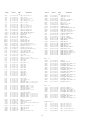
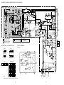
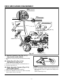
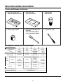
1
HV-FX7700
HV-BA75
HV-GX935
HV-FX7700, BA75
Z
Z
Z
HV-GX935
SERVICE MANUAL
STEREO VIDEO CASSETTE RECORDER
<7700/75>
VIDEO CASSETTE RECORDER<935>
BASIC VIDEO MECHANISM
: D33K-4HF/PAL(6721R-0250A)<7700/75>
: D33K-4HD/NP-VCR(6721R-0205A)<935>
S/M Code No. 09-007-347-2R3
DA
TA
RE
VI
SIO
N
This Service Manual is the "Revision Publishing" and replaces "Simple Manual"
(S/M Code No. 09-007-347-2T3).
TABLE OF CONTENTS
10. Base Assembly A/C Head ........................................ 70
11. Brake Assembly S .................................................... 71
12. Brake Assembly T .................................................... 71
13. Arm Assembly Tension ............................................. 71
14. Reel S & Reel T ....................................................... 71
15. Support CST ............................................................ 72
16. Base Assembly P4 ................................................... 72
17. Opener Lid ............................................................... 72
18. Arm Assembly T/up .................................................. 72
19. Arm Assembly Pinch ................................................ 72
20. Belt Capstan/Motor Capstan .................................... 73
21.Clutch Assembly D33-K ............................................ 73
22. Lever F/R ................................................................. 73
23. Gear Assembly H-Up/D-K or
Gear Assembly Up/D-K ............................................ 73
24. Bracket Assembly Jog .............................................. 74
25. Guide Rack F/L, Gear Rack F/L ............................... 74
26. Brake Assembly Capstan ......................................... 74
27. Gear Drive/Gear Cam/Gear Connector ................... 75
28. Bracket Assembly L/D motor .................................... 75
29. Gear Sector .............................................................. 76
30. Base Tension/Plate Slider/Lever Tension ................. 76
31. Gear Assembly P3/Gear Assembly P2 .................... 77
32. Base Assembly P3/Base Assembly P2 .................... 77
33. Arm Assembly Idler or Arm assembly Idler Jog ........ 77
DECK MECHANISM ADJUSTMENT
Tools and Fixtures for service ......................................... 78
1. Mechanism Alignment Position Check ....................... 79
2. Preparation for Adjustment ........................................ 80
3. Checking Torque ........................................................ 80
4. Guide Roller Height Adjustment ................................. 81
4-1. Preliminary Adjustment .......................................... 81
4-2. Precise Adjustment ................................................ 81
5. Audio/Control (A/C) Head Adjustment ........................ 82
5-1. Preliminary Adjustment .......................................... 82
5-2. Confirm that the Tape Path smoothly between
the Take-up Guide and Pinch Roller ..................... 83
5-3. Precise Adjustment (Azimuth Adjustment) ............. 83
6. X-Value Adjustment .................................................... 83
7. Adjustment after Replacing Drum Assembly
(Video Heads) ............................................................. 84
8. Check the Tape Travel after Reassembling
Deck Assembly ............................................................ 84
8-1. Checking Audio and RF Locking Time
during Playback and after CUE or REV ................ 84
8-2. Check for Tape Curling or Jamming ....................... 84
MAINTENANCE/INSPECTION PROCEDURE
1. Check before starting Repairs ................................... 85
2. Required Maintenance ............................................... 86
3. Scheduled Maintenance ............................................ 86
4. Supplies Required for Inspection and Maintenance .. 86
5. Maintenance Procedure ............................................. 86
5-1. Cleaning ................................................................. 86
5-2. Greasing ................................................................ 87
MECHANISM TROUBLESHOOTING GUIDE
1. Deck Mechanism ............................................... 88 ~ 90
2. Front Loading Mechanism ................................. 91 ~ 92
SPECIFICATIONS ............................................................ 3
ACCESSORIES LIST ....................................................... 3
DISASSEMBLY INSTRUCTIONS ..................................... 4
SERVICE POSITION ........................................................ 5
VCR TEST TAPE INTERCHANGEABILITY TABLE ........ 6
ELECTRICAL MAIN PARTS LIST .............................. 7 ~ 9
TRANSISTOR ILLUSTRATION ........................................ 9
WIRE HARNESS DIAGRAM .......................................... 10
BLOCK DIAGRAM ................................................. 11 ~ 22
SCHEMATIC DIAGRAM
1. POWER/TUNER/NICAM <7700/BA75> ............ 23 ~ 24
2. POWER/TUNER <935> ..................................... 25 ~ 26
3. AUDIO/VIDEO SECTION ................................... 29 ~ 30
4. Hi-Fi AUDIO/SCART <7700/BA75> ................... 31 ~ 32
5. SCART<935> ..................................................... 33 ~ 34
6. SYSTEM CONTROL/SERVO <7700/BA75> ..... 35 ~ 36
7. SYSTEM CONTROL/SERVO <935> ................. 39 ~ 40
8. KEY1 <7700/BA75> ................................................... 47
9. KEY2 <7700/BA75> ................................................... 47
10. KEY1 <935> ............................................................. 49
11. KEY2 <935> ............................................................. 49
WAVEFORM
AUDIO/VIDEO SECTION ............................................... 28
SYSTEM CONTROL/SERVO SECTION ....................... 38
VOLTAGE CHART
1. POWER SECTION ..................................................... 25
2. AUDIO/VIDEO SECTION ........................................... 27
3. Hi-Fi AUDIO/SCART SECTION ................................. 33
4. SYSTEM CONTROL/SERVO SECTION ................... 37
FL DISPLAY ............................................................ 41 ~ 42
WIRING
1. MAIN C.B <7700/BA75> .................................... 43 ~ 44
2. MAIN C.B <935> ................................................ 45 ~ 46
3. KEY1 C.B <7700/BA75> ............................................ 48
4. KEY2 C.B <7700/BA75> ............................................ 48
5. KEY1 C.B <935> ........................................................ 50
6. KEY2 C.B <935> ........................................................ 50
7. NICAM C.B ................................................................. 51
ADJUSTMENT ........................................................ 52 ~ 53
IC DESCRIPTION ................................................... 54 ~ 57
MECHANICAL EXPLODED VIEW 1/1 ........................... 58
MECHANICAL MAIN PARTS LIST 1/1 ......................... 59
MECHANISM EXPLODED VIEW 1/3~3/3 .............. 60 ~ 64
MECHANISM MAIN PARTS LIST 1/3~3/3 ............. 61 ~ 65
DECK MECHANISM PARTS LOCATIONS
Top View .......................................................................... 66
Bottom View .................................................................... 66
DECK MECHANISM DISASSEMBLY
1. Drum Assembly ......................................................... 67
2. Plate Assembly Top ................................................... 69
3. Holder Assembly CST ............................................... 69
4. Guide CST ................................................................ 69
5. Bracket Side (L)/Bracket Assembly Door .................. 69
6. Arm Assembly F/L ..................................................... 69
7. Lever Assembly S/W ................................................. 69
8. Arm Assembly Cleaner .............................................. 70
9. Head F/E ................................................................... 70
2
SPECIFICATIONS
<HV-FX7700, BA75>
Video recording system
Video head
Tuner system
TV system
Video signal system
Usable cssettes
Recording/playback time
<HV-GX935>
Video recording system
Video head
Tuner system
TV system
Video signal system
Usable cssettes
Recording/playback time
Rotary 2 head helical scanning system
Double azimuth 4 heads
Frequency synthesized tuner
B/G
PAL color signal, 625 lines, 50 fields
VHS video cassettes
PAL/MESECAM
SP: 5 hours max. with E-300 tape.
LP: 10 hours max. with E-300 tape
NTSC (Playback only)
SP: 3 hours 30 minutes max.
with T-210 tape
LP: 7 hours max.
with T-210 tape
EP: 10 hours 30 minutes max.
with T-210 tape
Tape speed
PAL/MESECAM
SP: 23.39 mm/s
LP: 11.69 mm/s]
NTSC (Playback only)
SP: 33.35 mm/s
LP: 16.67 mm/s
EP: 11.12 mm/s
Rewind time:
Approx. 3 min. with E-180 tspe
Channel coverage
VHF: C02 to C12
UHF: C21 to C71
CATV: S01 to S41
Video input
0.5 - 2.0 Vp-p, 75 ohm, unbalanced
Video output
1.0 Vp-p, 75 ohm, unbalanced
Horizontal resolution
240 lines (SP)
Video S/N
43 dB (SP)
Audio track
3 tracks (Hi-Fi sound 2 tracks, Normal
sound 1 track)
Audio input
SCART: -6 dBm, more than 10 k ohm
Audio output
SCART: -6 dBm, less than 1 k ohm
Hi-Fi frequency response 20 Hz - 20 kHz
Hi-Fi dynamic range
More than 87 dB (SP)
Hi-Fi wow & flutter
Less than 0.01% (nominal)
Operating temperature:
5 °C to 35 °C
Power requirements
200 - 240 V AC, 50 Hz
Power consumption
19 watts
TYPE 2.1 watts (power save mode.)
Dimensions
360 (W) x 270 (D) x 94.5 (H) mm
(141/4 x 103/4 x 33/4 in.)
Weight
Approx. 3.5 kg (7.7 lbs.)
Tape speed
Rewind time:
Channel coverage
Video input
Video output
Horizontal resolution
Video S/N
Audio track
Audio input
Audio output
Operating temperature:
Power requirements
Power consumption
Dimensions
Weight
Rotary 2 head helical scanning system
2 heads
Frequency synthesized tuner
B/G
PAL color signal, 625 lines, 50 fields
VHS video cassettes
PAL/MESECAM
5 hours max. with E-300 tape.
NTSC (Playback only)
3 hours 30 minutes max.
with T-210 tape
PAL/MESECAM
23.39 mm/s
NTSC (Playback only)
33.35 mm/s
Approx. 3 min. with E-180 tspe
VHF: C02 to C12
UHF: C21 to C71
CATV: S01 to S41
0.5 - 2.0 Vp-p, 75 ohm, unbalanced
1.0 Vp-p, 75 ohm, unbalanced
240 lines
43 dB
1 track (Normal sound)
SCART: -6 dBm, more than 10 k ohm
SCART: -6 dBm, less than 1 k ohm
5 °C to 35 °C
200 - 240 V AC, 50 Hz
16 watts
TYPE 2.1 watts (power save mode.)
360 (W) x 270 (D) x 94.5 (H) mm
(141/4 x 103/4 x 33/4 in.)
Approx. 3.5 kg (7.7 lbs.)
• Design and specifications are subject to change without notice.
ACCESSORIES LIST
REF. NO
PART NO.
KANRI
NO.
DESCRIPTION
1
1
1
2
2
S8-35R-P00-55J
S8-35R-P00-54J
S8-35R-P00-54L
S7-11R-1P0-24C
S7-11R-1P0-24D
INSTRUCTION ASSY ABFA918P 3GA1<75>
INSTRUCTION ASSY CBFA918P NGA2<77>
INSTRUCTION ASSY CBFA203P NSA4<93>
REMOTE CONTROLLER ASSY<75,77>
REMOTE CONTROLLER ASSY(BFA203P<93>
3
3
4
5
S8-610-33B-000
S8-615-05B-000
S8-615-05R-000
S5-640-18B-000
CABLE SET ASSY<75,77>
CABLE SET ASSY<93>
CABLE ASSY<75,77>
PLUG ASSY PHONO CORD<75,77>
TYPE
<77>
<75>
<93>
3
MODEL NAME SUFFIX
HV-FX7700
Z
HV-BA75
Z
HV-GX935
Z
DISASSEMBLY INSTRUCTIONS
1. Top Case Removal
1) Remove 4 screws holding the top case.
4. Mechanism Removal (see Fig. 3)
1) Disconnect the drum FF cable from the connector
(PMD01) on the Main C.B.
2) Disconnect the ACE head FF cable from the connector
(P3D02) on the Main C.B.
3) Remove 6 screws A .
2. Panel Front Removal (see Fig. 1)
1) Release 7 tabs, and then remove the panel front.
P3D02
PMD01
A
FF CABLE
PANEL
FRONT
FF CABLE
A
A
TAB
Fig. 1
Fig. 3
3. Key1 C.B. and Key2 C.B. Removal (see Fig. 2)
1) Release 2 tabs, and then remove Key2 C.B. from the connector (PKM02) in the direction of arrow 1 .
2) Release the tab, and then remove Key1 C.B. from the
connector (PKM01) in the direction of arrow 2 .
5. Main C.B. Removal (see Fig. 4)
1) Remove 2 screws B holding the panel assy, distri-butor.
2) Release 5 tabs, and then simultaneously lift the panel assembly, distributor and Main C.B. to remove them.
B
TAB
PANEL ASSY,
DISTRIBUTOR
1
PKM02
TAB
2
TAB
TAB
TAB
TAB
TAB
KEY2 C.B
MAIN C.B
KEY1 C.B
TAB
PKM01
Fig. 2
MAIN C.B
Fig. 4
4
SERVICE POSITION
To set the mechanism to the service position in active status:
Insert a spacer as shown below: The service position can be set in the stable status without any defective contact.
MAIN C.B
D33
MECHA
SPARSER
60mm
MAIN C.B
D33 MECHANISM
REAR PANEL
SPARSER
Location
Install spacers at locations (A) and (B).
CYLINDER
A
HEAD CLEANER
Top View
5
B
VCR TEST TAPE INTERCHANGEABILITY TABLE
There are two types of the new allgnment tape CH-1B (for NTSC) and CH-2 (for PAL). On each tape four signals (1)-(4)
are recorded for the times and in the order shown below.
(1) : 8min. → (2) : 2min. → (3) : 5min. → (4) : 5min.
The TTV-MP1 (for M-PAL), TTV-MS1 (for MESECAM) and TTV-S1 (for SECAM) allgnment tapes have the same
contents as the previous tapes.
Now in use TYPE
New TYPE
Method
Application
Model
Contents *1
Model
Contents *1
TTV-N1
NTSC, Color bar,
1 kHz, SP
TTV-NS1
NTSC, Color bar,
1 kHz, SP
TTV-N1E
NTSC, Color bar,
1 kHz, EP
TTV-NS6E
NTSC, Color bar,
No sound, EP
TTV-N2
NTSC, Stairsteps,
7 kHz, SP
CH-1B(1)
NTSC, Stairsteps,
7 kHz, SP
Head ACE Azimuth ADJ.
TTV-N12 NTSC, Color bar,
(SCV-1998) 1 kHz, SP
CH-1B(4)
NTSC, Color bar,
1 kHz, EP
FM Envelope ADJ.
X-Value ADJ.
NTSC
CH-1B(2)
NTSC, Stairsteps,
1 kHz, SP
No Changed.
CH-1B(4)
*2
PB-Y Level/General electrical ADJ.
Head ACE Height/Tilt ADJ.
For S-VHS (SQPB) check
NTSC, Color bar,
1 kHz, EP
No Changed.
Switching position ADJ.
For S-VHS (SQPB) check
TTV-N6
(TTV-N06T)
NTSC, Mono scope,
7 kHz, SP
TTV-N7A
NTSC, Stairsteps,
CH-1B(3)
1 kHz, SP, HiFi 400 Hz
NTSC, Color bar,
No sound SP,
HiFi 400 Hz
HiFi Audio PB Level ADJ.
TTV-P1
PAL, Color bar,
1 kHz, SP
CH-2 (2)
*3
PAL, Stairsteps,
1 kHz, SP
Switching position ADJ.
PB-Y Level/General electrical ADJ.
Head ACE Height/Tilt ADJ.
TTV-P1L
PAL, Color bar,
1 kHz, LP
CH-2 (4)
PAL, Color bar,
1 kHz, LP
Switching position. (LP Model)
FM Envelope ADJ. (LP Model)
X-Value ADJ. (LP Model)
TTV-P2
PAL, Stairsteps,
6 kHz, SP
CH-2 (1)
PAL, Stairsteps,
6 kHz, SP
HEAD ACE Azimuth ADJ.
FM Envelope ADJ. (SP Model)
X-Value ADJ. (SP Model)
TTV-P6
(TTV-N06T)
PAL, Monoscope,
6 kHz, SP
No Changed.
For total picture quality check (resolution, etc)
PAL
TTV-P7
TTV-P16
PAL, Stairsteps,
1 kHz, SP,
HiFi 1 kHz
PAL, Color bar,
400 Hz,
SP, HiFi 1 kHz
No Changed.
CH-2 (3)
For total picture quality check (resolution, etc)
PAL, Color bar,
No sound
SP, HiFi400 Hz
No Changed.
HiFi Audio PB Level ADJ.
FM Filter ADJ.
* 1. Described in the order of color format. video signal. linear audio. tape speed and Hi-Fi audio.
* 2. Use CH-1B (1)-(3) with models used exclusively in the SP mode.
* 3. Use CH-2 (3) and (4) when it is necessary to observe the chroma signal.
6
ELECTRICAL MAIN PARTS LIST
REF. NO
PART NO.
KANRI
NO.
DESCRIPTION
REF. NO
IC
!
!
S2-309-024-040
SI-SS4-310-00A
SA-400-811-220
SI-SA7-159-80A
SI-HI6-432-19A
SENSORLTV-817B PHOTO COU
IC,KA431AZ
KA7552
IC,LA71598M
IC,HD6432197XA04F
SI-SS3-082-00A
SI-AL2-416-00B
SI-KE7-031-00A
87-001-196-010
SI-NE1-631-10A
IC,KA3082
IC,AT24C16-10PC
IC,KIA7031P
IC,KIA7042P
IC,UPD16311GC-AB6
SI-IT3-407-00B
SI-SA7-479-30A
SI-PH9-605-00A
SI-MT1-443-00A
IC,MSP3407D-QG<75,77>
IC,LC74793<75,77>
IC,TDA9605H<75,77>
IC,MM1443XJ<75,77>
TRANSISTOR
!
ST-R12-730-9AA
ST-R32-050-9AB
ST-R12-680-9BA
S7-A30-293-010
S3-1KR-A10-3M0
TR,KTA1273-TP-Y
TR,KTC3205-TP-Y
TR,KTA1268-BL
TR,KTC2804-Y
TR,KRA103M-TP
ST-R10-030-9AA
ST-R31-990-9AF
SK-RC1-01M-000
ST-R12-670-9AC
ST-R53-430-9BA
TR,KSR1003
TR,KTC3199-BL
TR,KRC101M
TR,KTA1267-GR
TR,2SC5343-L
ST-R19-800-9CA
ST-R53-440-9AA
ST-R10-300-9AE
ST-R12-010-9AC
ST-F38-002-0AA
TR,2SA1980G
TR,2SC5344Y
TR,KRC103M
TR,SRC1201 4.7K,
TR,SSSS3N80A
SD-D01-000-9CA
SD-R18-020-9AA
SD-R10-400-9BA
SD-R81-004-0BA
SD-R20-200-0AB
DIODE,EG01CW
DIODE,ERA18-02KFRB
DIODE,RL104F
DIODE,ERC81-004L22
DIODE,HER202 BK
SD-D20-700-0AA
87-A40-246-080
SD-R10-400-9AB
87-070-173-010
DIODE,2A07
DIODE,1N4148
DIODE,RL104
DIODE,S1WBA60
PART NO.
KANRI
NO.
DESCRIPTION
C315
C316
C318
C320
C322
87-015-681-080
87-015-681-080
87-015-695-080
87-015-695-080
87-015-684-080
CAP,E
CAP,E
CAP,E
CAP,E
CAP,E
10-16V
10-16V
1.0-50V
1.0-50V
47-16V
C325
C326
C327
C333
C337
87-015-695-080
87-015-681-080
87-015-681-080
87-015-681-080
87-015-698-080
CAP,E
CAP,E
CAP,E
CAP,E
CAP,E
1.0-50V
10-16V
10-16V
10-16V
4.7-50V
C339
C346
C348
C354
C358
87-015-698-080
87-015-684-080
87-015-695-080
87-015-684-080
87-015-695-080
CAP,E
CAP,E
CAP,E
CAP,E
CAP,E
4.7-50V
47-16V
1.0-50V
47-16V
1.0-50V
C374
C376
C377
C379
C386
87-015-684-080
87-015-681-080
87-015-681-080
87-010-403-040
87-010-552-040
CAP,E
CAP,E
CAP,E
CAP,E
CAP,E
47-16V
10-16V
10-16V
3.3-50V
22-16V
C389
C390
C392
C500
C500
87-015-698-080
87-010-552-040
87-010-408-040
87-016-040-080
87-016-455-080
CAP,E 4.7-50V
CAP,E 22-16V
CAP,E 47UF-50V
CAP,0.047F-5.5V<93>
CAP,E 470UF-6.3V<75,77>
C502
C503
C504
C505
C510
87-015-684-080
87-016-088-040
87-016-088-040
87-015-684-080
87-015-684-080
CAP,E
CAP,E
CAP,E
CAP,E
CAP,E
47-16V
220-6.3V
220-6.3V
47-16V
47-16V
C523
C524
C526
C53O
C534
87-010-552-040
87-015-684-080
87-010-408-040
87-015-681-080
87-015-698-080
CAP,E
CAP,E
CAP,E
CAP,E
CAP,E
22-16V
47-16V
47UF-50V
10-16V
4.7-50V
C535
C546
C561
C591
C5A5
87-015-698-080
87-010-408-040
87-016-088-040
87-016-455-080
87-015-695-080
CAP,E
CAP,E
CAP,E
CAP,E
CAP,E
4.7-50V
47UF-50V
220-6.3V
470UF-6.3V
1.0-50V
C5F2
C5F3
C5P9
C701
C703
87-010-408-040
SC-E22-73D-638
87-015-698-080
87-015-698-080
87-015-698-080
CAP,E
CAP,E
CAP,E
CAP,E
CAP,E
47UF-50V
220-10V
4.7-50V
4.7-50V
4.7-50V
C704
C706
C713
C7M2
C7V1
87-015-684-080
87-016-455-080
87-015-684-080
87-015-681-080
87-015-684-080
CAP,E
CAP,E
CAP,E
CAP,E
CAP,E
47-16V
470UF-6.3V
47-16V
10-16V
47-16V<75,77>
C7V6
C7V7
C7V8
C806
C807
87-015-698-080
SC-N10-50K-948
87-015-695-080
87-015-698-080
87-015-698-080
CAP,E 4.7-50V<75,77>
CAP,1UF-50V<75,77>
CAP,E 1.0-50V<75,77>
CAP,E 4.7-50V<75,77>
CAP,E 4.7-50V<75,77>
C810
C811
C813
C814
C815
87-015-681-080
87-015-681-080
87-015-681-080
87-015-681-080
87-015-681-080
CAP,E
CAP,E
CAP,E
CAP,E
CAP,E
10-16V<75,77>
10-16V<75,77>
10-16V<75,77>
10-16V<75,77>
10-16V<75,77>
C816
C817
C818
C819
C821
87-015-681-080
87-015-681-080
87-015-698-080
87-015-681-080
87-015-684-080
CAP,E
CAP,E
CAP,E
CAP,E
CAP,E
10-16V<75,77>
10-16V<75,77>
4.7-50V<75,77>
10-16V<75,77>
47-16V<75,77>
C822
C823
C824
C825
C827
87-015-681-080
87-015-681-080
87-015-681-080
87-015-684-080
87-015-681-080
CAP,E
CAP,E
CAP,E
CAP,E
CAP,E
10-16V<75,77>
10-16V<75,77>
10-16V<75,77>
47-16V<75,77>
10-16V<75,77>
DIODE
MAIN C.B
BD141
!C101
!C102
!C103
!C105
S6-360-04C-000
S6-240-88K-000
S6-240-88K-000
SC-E47-6CU-611
87-016-375-010
COIL,BFS3550R2FD8
CAP,0.1UF-275VAC
CAP,0.1UF-275VAC
CAP,E 47UF-400V
CAP,0.01UF-630V
!C106
!C112
!C113
C115
C116
S6-240-87B-000
87-012-379-010
SA-1B3-0KH-2M0
87-010-408-040
87-010-237-910
CAP,100P-1KV
CAP,3300PF-400V
CAP,220PF-400V
CAP,E 47UF-50V
CAP,E 1000UF-16V
C117
C118
C119
C120
C121
87-010-375-080
SC-E22-73D-638
87-010-408-040
87-010-387-010
87-010-387-080
CAP,E
CAP,E
CAP,E
CAP,E
CAP,E
330-10V
220-10V
47UF-50V
470UF-25V KME
470UF-25V
C124
C144
C151
C153
C303
87-015-681-080
87-010-408-040
87-015-681-080
87-015-681-080
87-015-695-080
CAP,E
CAP,E
CAP,E
CAP,E
CAP,E
10-16V
47UF-50V
10-16V
10-16V
1.0-50V
C304
C310
87-015-684-080
87-015-698-080
CAP,E 47-16V
CAP,E 4.7-50V
7
REF. NO
PART NO.
KANRI
NO.
DESCRIPTION
REF. NO
PMK01
PMK02
PML01
PW101
R/C5F1
C828
C832
C835
C902
C912
87-015-684-080
87-015-684-080
87-010-400-080
87-016-455-080
87-016-455-080
CAP,E
CAP,E
CAP,E
CAP,E
CAP,E
47-16V<75,77>
47-16V
0.47-50V<75,77>
470UF-6.3V
470UF-6.3V<75,77>
C956
C960
C961
C962
C963
87-015-695-080
87-015-695-080
87-015-695-080
87-015-695-080
87-010-552-040
CAP,E
CAP,E
CAP,E
CAP,E
CAP,E
1.0-50V
1.0-50V
1.0-50V<75,77>
1.0-50V<75,77>
22-16V<75,77>
C964
CS501
DIG501
DIG501
ES501
87-015-695-080
S6-00R-DB0-04C
S3-02R-1N0-03B
S3-02R-1N0-03A
S9-31R-001-6A0
ES502
!F101
!F102
!FH01
!FH02
PART NO.
KANRI
DESCRIPTION
NO.
S5-618-43D-000
CONN,TUC-P05P 5P
S6-724-34B-000
CONN ASSY 5P-150
S6-30R-2S0-11A
CONN,2P
S5-612-92B-000
GP390 LGC 3P STRAIG P
S7-12R-293-8GA
REMOCON RECEIVER
!R101
R149
RS501
RS502
!T101
S6-140-07R-000
87-022-603-080
S5-00R-AB0-02A
S5-00R-AB0-02A
S6-420-23U-000
RES,2.7-2W
RES,FIX O 0.47-2W
SENSOR GP1S566
SENSOR GP1S566
TRANSFORMER,SMPS SJE-023U
CAP,E 1.0-50V<75,77>
SW,MPU10252MLB4 MIC
LEVEL METER 7MT229GK<93>
DH 9MT168GK<75,77>
SENSOR END
TU701
TU701
W101
X301
X501
S7-00R-PL0-1B0
S7-00R-PG0-1E0
87-005-440-080
S2-02R-244-3AE
S2-02R-310-01F
TUNER TADC-G102D<93>
TUNER TCMK0601PD11C<75,77>
COIL,47M 6-6-5<75,77>
CRYSTAL,STANDARD H49U
X’TAL,10.0000
S9-31R-001-6A0
S5-850-11T-000
87-001-196-010
S5-860-08B-000
S5-860-08B-000
SENSOR END
FUSE,1600MA 250V
ICP-N10 T104
HOLDER,FUSE CLIP
HOLDER,FUSE CLIP
X502
X503
ZD104
ZD141
ZD142
S5-290-01K-000
S2-02R-317-71E
SD-Z56-260-9AA
SD-Z22-000-9ED
87-A40-458-080
X’TAL,32.768KHZ
X’TAL,17.734476MHZ
ZENER,GDZJ5.6B 26MM TP
ZENER,MTZ22B
ZENER,MTZ18B
FL301
JK801
JK901
JK901
!L102
S6-330-32K-000
S6-12R-C00-2C0
S6-20R-M00-02B
S6-20R-M00-02A
S6-161-45H-000
COIL,OSC BIAS 1CHIP 5V
JACK,RCA RCA-208C-06<75,77>
SOCKET 1F-21P<93>
SOCKET 2F-21P<75,77>
FILTER SHT LFS2020V4-04350
ZD151
ZD501
ZD503
ZD701
ZD801
SD-Z13-260-9AB
SD-Z68-260-9AB
SD-Z68-260-9AB
SD-Z33-260-9AA
SD-Z51-000-9AJ
ZENER,GDZJ13A 26MM
ZENER,GDZJ6.8C
ZENER,GDZJ6.8C
ZENER,GDZJ33B 26MM TP
ZENER,GDZJ5.1B TP
L103
L104
L105
L301
L302
S6-330-88G-000
S6-330-88G-000
87-003-152-080
87-005-196-080
87-003-286-080
COIL,CHOCK TP 5MM
COIL,CHOCK TP 5MM
INDUCTOR,100M 2.3-3.4-5
COIL,10UH
COIL,56 2.3-3.4-5
ZD802
ZD803
ZD804
ZD805
ZD806
SD-Z56-260-9AA
SD-Z13-260-9AB
SD-Z13-260-9AB
SD-Z51-000-9AJ
SD-Z51-000-9AJ
ZENER,GDZJ5.6B 26MM TP
ZENER,GDZJ13A 26MM<75,77>
ZENER,GDZJ13A 26MM<75,77>
ZENER,GDZJ5.1B TP
ZENER,GDZJ5.1B TP
L303
L303
L305
L307
L308
87-003-286-080
87-003-152-080
87-005-196-080
87-005-196-080
87-005-440-080
COIL,56 2.3-3.4-5<93>
INDUCTOR,100M 2.3-3.4-5<75,77>
COIL,10UH
COIL,10UH
COIL,47M 6-6-5
L310
L503
L504
L505
L506
87-005-196-080
87-005-196-080
87-005-196-080
87-005-196-080
87-005-686-080
COIL,10UH
COIL,10UH
COIL,10UH
COIL,10UH
COIL,15UH
PKM01
SW905
SW905
SW906
SW906
S5-618-44D-000
S5-562-19B-000
S5-562-82C-000
S5-562-19B-000
S5-562-82C-000
CONN,5P
SW,SKHV10910B<93>
SW,SKQNQED ALPS 5MM<75,77>
SW,SKHV10910B<93>
SW,SKQNQED ALPS 5MM<75,77>
L5F1
L5S1
L702
L703
L704
87-005-196-080
87-003-148-080
87-005-196-080
87-005-196-080
87-003-145-080
COIL,10UH
INDUCTOR,33
COIL,10UH
COIL,10UH
INDUCTOR,8.2
SW907
SW907
SW908
SW908
SW909
S5-562-19B-000
S5-562-82C-000
S5-562-19B-000
S5-562-82C-000
S5-562-19B-000
SW,SKHV10910B<93>
SW,SKQNQED ALPS 5MM<75,77>
SW,SKHV10910B<93>
SW,SKQNQED ALPS 5MM<75,77>
SW,SKHV10910B<93>
L705
L7V1
L801
L8R1
L8R2
87-005-696-080
87-005-196-080
87-005-196-080
87-003-152-080
87-003-152-080
COIL,100UH
COIL,10UH<75,77>
COIL,10UH
INDUCTOR,100M 2.3-3.4-5<75,77>
INDUCTOR,100M 2.3-3.4-5<75,77>
SW909
SW910
SW910
SW911
SW911
S5-562-82C-000
S5-562-19B-000
S5-562-82C-000
S5-562-19B-000
S5-562-82C-000
SW,SKQNQED ALPS 5MM<75,77>
SW,SKHV10910B<93>
SW,SKQNQED ALPS 5MM<75,77>
SW,SKHV10910B<93>
SW,SKQNQED ALPS 5MM<75,77>
SW912
S5-562-19B-000
SW,SKHV10910B<93>
L901
L902
L904
L905
L906
87-003-152-080
87-003-152-080
87-003-152-080
S6-360-04C-000
87-003-152-080
INDUCTOR,100M 2.3-3.4-5
INDUCTOR,100M 2.3-3.4-5
INDUCTOR,100M 2.3-3.4-5
COIL,BFS3550R2FD8
INDUCTOR,100M 2.3-3.4-5
L907
L911
L912
L914
L916
S6-360-04C-000
87-003-152-080
87-003-152-080
87-003-152-080
87-003-152-080
COIL,BFS3550R2FD8
INDUCTOR,100M 2.3-3.4-5<75,77>
INDUCTOR,100M 2.3-3.4-5<75,77>
INDUCTOR,100M 2.3-3.4-5<75,77>
INDUCTOR,100M 2.3-3.4-5<75,77>
LD901
LED902
PKM02
SW901
SW902
SD-L53-110-0AA
SD-L53-110-0AA
S5-610-36D-000
S5-562-82C-000
S5-562-82C-000
LED,SG5311(GRN)<93>
LED,SG5311(GRN)<75,77>
MA V 8283-0512 WH ELCO
SW,SKQNQED ALPS 5MM<75,77>
SW,SKQNQED ALPS 5MM<75,77>
SW903
SW903
SW904
SW904
S5-562-19B-000
S5-562-82C-000
S5-562-19B-000
S5-562-82C-000
SW,SKHV10910B<93>
SW,SKQNQED ALPS 5MM<75,77>
SW,SKHV10910B<93>
SW,SKQNQED ALPS 5MM<75,77>
LD501
MS501
P3D01
P3D01
P3D02
S9-31R-001-7A0
S6-00R-PY0-01B
S5-612-34Z-000
S5-612-34W-000
S6-30R-5S0-08E
LED
SW,MMS00420ZMBO MIC
CONN,3P<93>
GF120-10S-TS-A LGC 10P MP<75,77>
CONN,6P
P3D03
P7M01
P7M02
PMC01
PMD01
S5-612-51B-000
S5-618-48F-000
S5-618-48F-000
S6-30R-BE0-1H0
S5-612-34V-000
GB201-2P-TS-B(LGC) P
CABLE 2P<75,77>
CABLE 2P<75,77>
CONN,8P
GF120-07S-TS LGC 7P SP
KEY 1 C.B
KEY 2 C.B
NICAM C.B<75,77>
8
C751
C757
C758
C759
C762
87-015-684-080
87-015-684-080
87-015-681-080
87-015-681-080
SC-Q39-21N-409
CAP,E 47-16V<75,77>
CAP,E 47-16V<75,77>
CAP,E 10-16V<75,77>
CAP,E 10-16V<75,77>
CAP,0.0039U 100V<75,77>
C763
SC-Q39-21N-409
CAP,0.0039U 100V<75,77>
REF. NO
PART NO.
C766
C769
C770
L751
L752
KANRI
DESCRIPTION
NO.
87-010-403-040
CAP,E 3.3-50V<75,77>
87-015-681-080
CAP,E 10-16V<75,77>
87-015-684-080
CAP,E 47-16V<75,77>
87-005-196-080
COIL,10UH<75,77>
87-005-196-080
COIL,10UH<75,77>
L753
L754
L755
X751
87-005-196-080
87-003-129-080
87-003-129-080
S5-290-219-000
COIL,10UH<75,77>
INDUCTOR,6800<75,77>
INDUCTOR,6800<75,77>
X’TAL 18.432MHZ<75,77>
TYPE
<77>
<75>
<93>
MODEL NAME SUFFIX
HV-FX7700
Z
HV-BA75
Z
HV-GX935
Z
TRANSISTOR ILLUSTRATION
ECB
KRA103M
KRC103M
KTA1267
KTC101M
KTC3199
ECB
2SA1980
2SC5343
2SC5344
KSR1003
KTA1268
SRC1201
GDS
SSS3N80A
9
ECB
KTA1273
KTC3205
ECB
KTC2804
WIRE HARNESS DIAGRAM
P7M01
PM701
1
1
A.MUTE "H"
2
TU.A.L
2
3
TU.A.R
3
4
BBE A.OUT.R
4
5
NICAM C.B
<7700>
NC
5
6
NC
6
7
12VT
7
8
BBE A.LOUT
8
9
NC
9
P7M02
1
GND
PM702
1
2
DATA
2
3
CLK
3
4
GND
4
5
SIF
5
6
5V
6
7
NC
7
8
TU.MONO.AUD
8
9
GND
9
PMD01
PDM01
1
D.CTL
1
2
M.GND
2
3
DFG
3
4
12V
4
5
PG
5
6
GND
6
7
5.1V
7
PMC01
<7700,75>
PKM02
KEY 2 C.B
1
2
3
4
5
PMK02
1
5.2VA
OTPB LED "H" 2
3
KEY RTN 1
4
GND
POWER KEY 5
MAIN C.B
PKM02
KEY 1 C.B
1
2
3
4
5
PMK02
1
NC
2
NC
3
KEY RTN1
4
5.2VA
5
GND
LOWER
DRUM
PCM01
GND
1
2 MOTOR GND
I-LIMIT
3
CAP CTL
4
12.3VA
5
CFG
6
7 CAP REV "L"
5.1V
8
1
2
3
4
5
6
7
8
CAPSTAN
MOTOR
P3D02
CTL(+)
1
CTL(-)
2
A/E(-)
3
A/E(+)
4
A.REC
5
A.PB
6
1
2
3
4
5
6
ACE
HEADS
MS501
GND
1
MODE S1
2
MODE S2
3
MODE S3
4
MODE S4
5
1
2
3
4
5
MS501
MODE SW
P3D03
1
GND
2 FULLERASE
1
2
FULL ERASE
HEAD
P3D01
<7700,75>
<935>
KEY2 C.B
PKM01
PMK01
1
5.2VA
1
2 OTPB LED "H" 2
3
3 KEY RTN 1
4
GND
4
5 POWER KEY 5
<935>
1
2
3
4
5
6
7
1 8
2 9
3 10
Hi-Fi A PB
Hi-Fi REC
Hi-Fi B PB
SP A PB
SP REC
SP B PB
LP A PB
LP REC
LP B PB
1
2
3
4
5
6
7
8
9
10
CYL.
HEADS
PML01
KEY1 C.B
1
2
PKM01
PMK01
1
GND
1
2
2 KEY RTN 1
3
NC
3
4
NC
4
5
NC
5
6
5
4
3
2
1
10
LD(+)
LD(-)
PMJ01
FLD DATA MS
FLD DATA SW
MDO
RES
5.4VA
GND
1
2
LOADING
MOTOR
3
4
2
11
BK
WH
(BR)
(BL)
PW101
AC INPUT
!
F101
!
!
+
NOTES :
!
R101 !
C113
(C101,L102,
C102)
LINE FILTER
BLOCK
R141,142,143
D141
1
BD101
(D102,R104,
C105,C106)
3
4
1
2
IC102
4
6
!
HOT CIRCUIT
Symbol denotes DC chassis ground.
Symbol denotes AC ground.
!
HOT GND
ZD141,R149,R147,R148)
(IC141,C142,C141,R146,C143,
!
S/W BLOCK &
OVER CURRENT LIMIT
BLOCK
R144,R145,D142,ZD142
Drive Block FET141 !
C112
!
C103
SNUBBER
BLOCK
!
15
14
13
12
8
7
11
10
9
TRANSFORMER
T101 !
2
1
(D105, C115)
RECTIFIER
& SMOOTHING
IC103
(R116,R117,R118
R119,R120,R121
C114)
FEED-BACK
BLOCK
(D106, C116,
L103,C117)
RECTIFIER
& SMOOTHING
(F102, D107, C118,
ZD104, C155, D108,
FR01, C119)
FLD Drive
(D109, C120,
L104,C121)
RECTIFIER
& SMOOTHING
D159
(Q166, R172,
R173)
(Q152, R153,
R154, D156)
5VT SW
BLOCK
Q164,
Q165
PWR CTL
BLOCK
(Q151, R151,
R152)
D158
Q163
(Q162, C124,
R161)
(Q155,R105, R159,
C153,ZD151,C151)
D155
5V S/W
BLOCK
D153 D154
12VA REG.
BLOCK
D152
D160
5VG S/W
BLOCK
(Q154, R157,
R158,R155)
36V S/W
BLOCK
Q157
D151
Switching
Q153, Q156
TIMER "H"
FROM -COM
FROM -COM
P.CTL"H"
TO System
5.2VG
TO AV,Hi-Fi, SYS
5.2V
TO AV, TU/IF,
SYSCON
5.2VT
TO SYS/HIFI
5.4VA
12V(DRUM)
TO SYS, DRUM
TO TU/IF
33V
TO HIFI/SYS
12VA
TO SYS
13VA
TO SYS
24/15/12V
TO SYS
-16VG, -21VG,
-27VG
F. -com
STANDBY "H"
BLOCK DIAGRAM-1 (POWER SECTION)
BLOCK DIAGRAM-2 (AUDIO SIGNAL SECTION) <HV-GX935>
JK901
MOD.A.OUT
21
BUF.V.IN
19
TU.A.L
17
20
To
POWER/
TUNER
SECTION
18
16
TU.V.IN
15
12
VIDEO OUT 1
11
10
VIDEO OUT 2
9
8
AUDIO OUT 1
7
6
AUDIO OUT 2
5
4
3
To
AUDIO/
VIDEO
SECTION
2
MONO A.IN
1
PB AUDIO SIGNAL
PB VIDEO SIGNAL
REC AUDIO SIGNAL
REC VIDEO SIGNAL
12
EURO AV1
AUDIO/VIDEO
14
13
BLOCK DIAGRAM-3 (AUDIO SIGNAL-Hi-Fi AUDIO SECTION) <HV-FX7700/BA75>
BUF.V.IN
TU.V.IN
IIC CLK
To
IIC DATA
SYSTEM
CONTROL/
A.ENV
SERVO/OSD
LP REC MUTE "H"
SECTION
A.H/SW
To
POWER/
TUNER
SECTION
AUDIO
IC801
TDA9605H
Hi-Fi AUDIO PROCESS
IC901
MM1443XJ
INPUT SELECT SW
OUT(R)
SORTIE G
OUT(L)
SORTIE D
JK901(1/2)
21
29 V.OUT3
E1.V 1
30 V.OUT2
E2.V 3
18
17
HiFi PB B
31 V.OUT1
EXT.V 5
16
15
TU.V 28
13
TU.A.L
11
TU.A.R
9
12
10
VIDEO OUT
To
AUDIO/
VIDEO
SECTION
8
EURO AV1
AUDIO/VIDEO
To
POWER/
TUNER
SECTION
14
HiFi REC
7
6
5
4
3
2
1
JK901(2/2)
42
MOD A.OUT
41
40
To
POWER/
TUNER
SECTION
39
38
37
36
35
MONO A.IN
AUDIO OUT 1
34
To
AUDIO/
VIDEO
SECTION
33
32
31
30
29
28
27
26
25
24
23
22
PB AUDIO SIGNAL
PB VIDEO SIGNAL
REC AUDIO SIGNAL
REC VIDEO SIGNAL
13
14
EURO AV2
DECODER
To
CYL.HEADS
20
19
HiFi PB A
BLOCK DIAGRAM-4 (VIDEO SECTION)
IC301
LA71598M
AUDIO/VIDEO
PROCESSOR
Q304
74
57
FROM
CYL.HEADS
54
51
61
C. COMB
72
71
LPF
46
Y
DELAY
45
Q303
C LPF
85
LP ’B’ PB
52
MAIN
CONV
ACC
82
LP ’A’ PB
59
43
41
SP ’B’ PB
88
SP ’A’ PB
91
NL
DE EMP
YNR
FM
DEM
PB FM
AGC
V. ENV
ENV
DET
93
11
18
17
IC7V1
LC74793
VPS/PDC DECODER
LPF
SUB
LPF
DOUBLE
LIMIT
PB EQ
10
Y/C
MIX
21
CLAMP
SERIAL
DECODER
20
23
6dB AMP
24
28
DATA
LATCH
29
6
PB
PEAKING
MAIN
DE-EMPH
7
IIC BUS
INTERFACE
Q302
16
SYNC
SEP
Q301
A.MUTE
"H"
COLOR A.AMP V.H S/W
ROTARY SW
CLOCK DATA C SYNC
V.OUT
(TO MICOM)
To
SYSTEM CONTROL/
SERVO/OSD
SECTION
:PB VIDEO SIGNAL
:PB YSIGNAL
:PB CHROMA SIGNAL
IC301
LA71598M
AUDIO/VIDEO
PROCESSOR
Q304
71
72
61
BPF
COMB
AMP
51
52
54
57
59
C. COMB
To
CYL.HEADS
46
Y
DELAY
BPF1
LP REC
45
84
Q303
CCD
LPF
90
SP REC
DATA
ACQUISITION
43
YNR
+
DETAIL
ENH
:REC CHROMA SIGNAL
FM
MOD
10
11
18
19
V. IN 2
S/W
FBC
32
SERIAL
DECODER
W/D
CLIP
36
38
NL EMPH
:REC Y SIGNAL
41
Y-LPF
REC FM
EQ
:REC VIDEO SIGNAL
<935>
To
SCART
SECTION
23
24
AGC
28
29
V. IN 1
To
Hi-Fi AUDIO/
SCART
SECTION
31
30
MAIN
EMPH
A.MUTE
"H"
COLOR A.AMP V.H S/W
ROTARY SW
R308,R309,
C309
C. SYNC
CLOCK DATA
REC ’H’
V.OUT
(TO MICOM)
To
SYSTEM CONTROL/
SERVO/OSD
SECTION
15
16
BLOCK DIAGRAM-5 (NORMAL AUDIO SECTION)
IC301
LA71598M
AUDIO/VIDEO
PROCESS
<935>
To
SCART
SECTION
FL301,Q311
AUDIO IN 2
78
AUDIO IN 1
76
To
Hi-Fi AUDIO/
SCART
SECTION
<7700,75>
LINE
AMP
ALC
AUTO
BIAS
REC
AMP
MUTE
99
CONTROL
Q307
BIAS
OSC
80
96
98
7
6
AUDIO
REC/PB
HEAD
To
SCART
SECTION
<935>
:REC AUDIO SIGNAL
IC301
LA71598M
AUDIO/VIDEO
PROCESS
1
AUDIO
REC/PB
HEAD
100
4
EQ AMP
Q308,
Q309,
Q310
6
LINE
AMP
Vref
MUTE
5
99
REC "H"
SERIAL
DECODER
AUDIO
BIAS
24
23
DATA
CLK
To
SYSTEM CONTROL/
SERVO/OSD
SECTION
:PB AUDIO SIGNAL
17
96
MONO A.OUT
To
Hi-Fi AUDIO/
SCART
SECTION
<7700,75>
To
SCART
SECTION
<935>
18
144
To
Hi-Fi AUDIO/
SCART
SECTION
27
To
SYSTEM CONTROL/
SERVO/OSD
SECTION
To
POWER
SECTION
To
Hi-Fi AUDIO/
SCART
SECTION
:REC VIDEO SIGNAL
:PB VIDEO SIGNAL
FM1/AM
FM2
NICAM A
NICAM B
IDENT
SCARTL
SCARTR
SCART1 R
SCART1 L
18,432MHz
Audio PLL
:REC AUDIO SIGNAL
:PB AUDIO SIGNAL
Demodulator
A/D
A/D
D/A
D/A
SCART Switching Facilities
D/A
LOUDSPEAKER L
X751
DSP
D/A
LOUDSPEAKER R
<7700,BA75>
IC751
MSP3417D-QG
NICAM/A2 BLOCK
To
POWER
SECTION
19
94
59
60
<935>
141 5.4VA
144
Q701
To
Hi-Fi AUDIO/
SCART
SECTION
875
To
SYSTEM CONTROL/
SERVO/OSD
SECTION
SORTIE
ANTENNE
RF.OUT
ENTREE
ANTENNE
AERIAL
BLOCK DIAGRAM-6 (TUNER, NICAM/A2 SECTION)
143 5.2VT
BLOCK DIAGRAM-7 (SYSTEM CONTROL/SERVO SECTION) <HV-FX7700/BA75>
MAIN (SYSTEM CONTORL/SERVO/OSD SECTION)C.B <7700,75>
9MT168GK
949
72,73
To
LOADING
MOTOR
To
Hi-Fi AUDIO/
SCART
SECTION
UPD16311GC
DISPLAY DRIVER
83,107
104
103
To
POWER/
TUNER
SECTION
To
LOWER DRUM
PDM01
84,108
9
IC501
HD6432197XA04F
SYSCON/SERVO/OSD
PROCESS
50
85
To
CAPSTAN
MOTOR
PCM01
29
949
28
38
To
AUDIO/
VIDEO
SECTION
51
TSOP1238SP1
ATC24C16-10PC
95
A37
77
88
MS501
37
59,60
3-8
17,19 18
78,80
10
21,22
68-71 49,92
36
75,76
56
39
19
11,12
A37
20
43
To
POWER/
TUNER
SECTION
BLOCK DIAGRAM-8 (SYSTEM CONTROL/SERVO SECTION) <HV-GX935>
MAIN (SYSTEM CONTORL/SERVO/OSD SECTION)C.B <935>
7MT229GK
949
72,73
To
LOADING
MOTOR
To
SCART
SECTION
UPD16311GC
DISPLAY DRIVER
83,107
104
103
To
POWER/
TUNER
SECTION
To
LOWER DRUM
PDM01
84,108
9
IC501
HD6432197XA04F
SYSCON/SERVO/OSD
PROCESS
50
85
To
CAPSTAN
MOTOR
PCM01
29
949
28 38
To
AUDIO/
VIDEO
SECTION
A.LEVEL(R)
A.LEVEL(L)
A.ENV
51
TSOP1238SP1
95
A37
77
88
MS501
59,60
37
3-8
17,19 18
78,80
10
21,22
68-71 49,92
36
75,76
56
39
21
11,12
A37
22
43
To
POWER/
TUNER
SECTION
SCHEMATIC DIAGRAM-1 (POWER/TUNER/NICAM SECTION) <HV-FX7700/BA75>
MAIN(POWER/TUNER SECTION)C.B <7700,75>
KRA18-02KFRB
6
7
KTC3205
8
4
22uH
To
SYSTEM
CONTORL/
SERVO/OSD
SECTION
9
ERA18-02KFRB
2
(DRUM)
10
LFS2020V404350
D
11
S
12
10u/16V
G
KRA103M
KSR1003
22uH
13
KRA103M
10u/16V
ERC81-004L22
To
Hi-Fi AUDIO/
SCART
SECTION
To
AUDIO/
VIDEO
SECTION
14
KTA1267-GR
1
To
SYSTEM
CONTORL/
SERVO/OSD
SECTION
15
KTA1273
KRA103M
KRC101M
KTA1273
1
3
2
KTC3199-BL
AC INPUT
10u/16V
ENTREE
ANTENNE
AERIAL
SORTIE
ANTENNE
RF.OUT
D/A
D/A
SCART Switching Facilities
SCARTL
SCARTR
IDENT
Demodulator
LOUDSPEAKER R
A/D
A/D
SCART1 R
SCART1 L
LOUDSPEAKER L
D/A
D/A
KTA1267-GR
C710
43P
DSP
FM1/AM
FM2
NICAM A
NICAM B
Audio PLL
18.432MHz
NICAM C.B <7700,75>
:REC VIDEO SIGNAL
:PB VIDEO SIGNAL
:REC AUDIO SIGNAL
:PB AUDIO SIGNAL
NOTES)
Symbol denotes AC ground.
NOTES)
Symbol denotes DC chassis ground.
NOTE)
NOTE)
NOTE)
NOTE)
Warning
Parts that are shaded are critical
With respect to risk of fire or
electricial shock.
To
Hi-Fi AUDIO/SCART
SECTION
23
To
SYSTEM CONTORL/
SERVO/OSD
SECTION
24
To
Hi-Fi AUDIO/SCART
SECTION
SCHEMATIC DIAGRAM-2 (POWER/TUNER SECTION) <HV-GX935>
MAIN(POWER/TUNER SECTION)C.B <935>
KRA18-02KFRB
6
7
KTC3205
8
4
22uH
To
SYSTEM
CONTORL/
SERVO/OSD
SECTION
9
ERA18-02KFRB
2
(DRUM)
10
D
LFS20201404350
11
10u/16V
G
KRA103M
12
S
KSR1003
22uH
13
KRA103M
10u/16V
ERC81-004L22
To
SCART
SECTION
To
AUDIO/
VIDEO
SECTION
14
KTA1267-GR
1
To
SYSTEM
CONTORL/
SERVO/OSD
SECTION
15
KTA1273
KRC101M
KTA1273
1
3
2
KTC3199-BL
AC INPUT
10u/16V
:REC VIDEO SIGNAL
:PB VIDEO SIGNAL
:REC AUDIO SIGNAL
:PB AUDIO SIGNAL
NOTES)
Symbol denotes AC ground.
NOTES)
Symbol denotes DC chassis ground.
VOLTAGE CHART-1 (POWER SECTION)
IC102
PB
4.0
0.0
0.0
PB
3.5
2.0
17.2 3.7
2.0
17.5 3.9
5
IC141
1
4.9
3.9
REC 4.9
4.0
C710
43P
1
1.1
1.3
0.0
0.0
REC 1.1
1.3
0.0
0.0
PB
IC103
IC103
SORTIE
ANTENNE
RF.OUT
KTA1267-GR
REC 3.5
IC102
Gate
ENTREE
ANTENNE
AERIAL
IC, KA7552
4
PB
Warning
Parts that are shaded are critical
With respect to risk of fire or
electricial shock.
IC BLOCK DIAGRAM-1
IC141
REC 4.0
NOTE)
NOTE)
NOTE)
NOTE)
TRANSISTOR
Anode
Cathode
PB
REC
PB
REC
PB
REC
2.5
2.5
0.0
0.0
3.9
3.9
Emitter
PB
Q151
11.9
REC
Collector
PB
REC
Base
PB
REC
11.8 14.8 15.0
12.5 12.4
10.0
Q152
9.4
9.3
Q153
11.8
11.7 14.8 15.0
11.8 11.6
9.9
12.4 12.3
Q154 -27.3 -27.9 -27.3 -27.8 -26.6 -27.0
Q155
5.3
5.3
5.2
5.3
0.0
0.0
Q156 -16.1 -16.5 -16.0 -16.4 -15.4 -15.7
Q157
5.3
5.3
Q158
35.6
36.0 35.3 35.7
5.2
5.2
0.0
0.0
Q159
5.3
5.3
5.2
5.2
4.5
4.5
Q160
0.0
0.0
0.0
0.0
5.0
5.0
Q161
0.0
0.0
0.1
0.0
5.0
5.0
Q162
5.3
5.3
5.2
5.2
4.5
4.5
Q164
5.3
5.3
5.3
5.3
4.6
4.6
Q165
0.0
0.0
10.0 10.0
0.0
0.0
35.0 35.4
NOTE:
Voltage are DC-measured with a digital voltmeter during TUNER mode.
25
To
SCART
SECTION
To
SYSTEM CONTORL/
SERVO/OSD
SECTION
26
To
SCART
SECTION
VOLTAGE CHART-2 (AUDIO/VIDEO SECTION)
IC301
PIN
PB
REC
PIN
PB
1
2.44
REC PIN
2.42
21
2.41
PB
REC PIN
2.52
41
2.93 2.92
PB
61
3.43
3.43
81
0
0
2
2.44
2.42
22
0
0
42
3.16 3.14
62
3.31
3.32
82
0.03
0.04
3
2.46
2.44
23
4.48
4.52
43
3.02 2.05
63
5
5
83
0
0
4
2.45
2.35
24
4.19
4.23
44
64
5
5
84
0.03
0.03
5
0.09
0.88
25
1.69
1.69
45
2.34 2.33
65
2.03
2.03
85
0.03
0.03
6
2.46
2.34
26
0.05
0.06
46
1.46 1.44
66
2.66
2.67
86
0
0
7
2.46
2.34
27
0.34
0.34
47
9.13 9.12
67
3.87
3.86
87
4.87
4.80
8
0
0
28
0.34
0.34
48
1.94 1.96
68
0
0
88
1.83
3.97
9
0
0
29
1.78
1.84
49
0.85 0.85
69
0.80
1.27
89
0
0
10
0.93
0.93
30
1.10
4.57
50
70
1.98
2.92
90
1.83
3.95
11
1.68
1.68
31
2.97
2.94
51
1.83 1.82
71
2.52
2.51
91
1.83
3.98
12
4.98
2.60
32
-
2.3
52
2.71 2.62
72
3.37
1.73
92
0.02
1.55
13
1.49
1.52
33
1.45
1.37
53
73
3.8
3.17
93
2.17
0.01
14
1.68
1.38
34
1.81
1.79
54
2.62 2.62
74
1.55
0.01
94
0
2.01
15
2.34
2.32
35
3.25
3.22
55
4.91 4.91
75
4.96
4.94
95
0
0
16
5.01
5.02
36
1.82
1.95
56
0.56 0.57
76
2.43
2.41
96
2.29
2.38
17
3.08
0.15
37
4.79
4.79
57
3.44 3.44
77
0.01
0.14
97
0
0
18
1.98
2.45
38
1.81
2.25
58
5.00 5.00
78
2.42
2.42
98
2.43
2.41
19
1.18
2.45
39
4.10
4.10
59
3.36 3.37
79
2.46
2.45
99
5.08
4.28
20
3.01
3.05
40
5.00
5.00
60
3.31 3.31
80
2.43
2.23 100 2.43
2.60
B
E
0
0
0
0
0
0
REC PIN
IC7V1
PIN
PB/ REC
1
0
2
2.6
3
5.1
4
5.1
5
0
6
4.8
7
4.9
8
5.1
9
4.7
10
0
11
2.2
12
2.2
13
0.9
14
0
15
5.1
16
3.0
17
2.6
18
4.7
19
5.1
20
5.0
21
0
22
4.5
23
5.1
24
0
TRANSISTOR
PB mode
E
C
REC mode
C
B
Q301 1.213 3.930 1.864 1.783 3.348 2.435
Q302 1.548 5.158 2.191 1.813 5.147 2.452
Q303 2.151
0
1.499 2.147
0
1.494
Q304 1.217 5.061 1.835 1.216 5.039 1.824
Q305 2.383
0
1.705 2.420
0
1.749
Q306 1.222
0
0.546 1.221
0
0.557
Q307 5.258 0.280 5.176 5.186 3.301 4.352
Q308
0
0
0.744 15.827
0
-21.49
Q309
0
0
0.720 -5.69
0
-21.77
Q310 5.256 5.180 4.053 5.189 -21.64 5.148
Q311 1.224 3.923 1.872 0.271 3.190 0.636
Q3A1
0
5.251
0
1.258 5.179 1.766
Q201 1.313 5.135 1.924 0.625 5.115 0.092
Q202 1.314 5.135 1.237 0.624 5.120 1.219
Q203
0
1.924 0.016
0
0.092 5.111
27
PB
REC
WAVEFORMS-1 (AUDIO/VIDEO SECTION)
1
2
IC301 Pin 38,
1Vp-p
Video in
IC301 Pin 20
500mVp-p
PB mode
5
3
IC301 Pin 6
2.2Vp-p
REC mode
7
IC301 Pin 29
2.1Vp-p
PB mode
10
9
13
IC301 Pin 67
600mVp-p
PB mode
11
14
IC301 Pin 66
600mVp-p
PB mode
8
IC301 Pin 41
400mVp-p
PB mode
IC301 Pin 24
5Vp-p
PB/REC modes
IC301 Pin 23
5Vp-p
PB/REC modes
IC301Pin 7
1.4Vp-p
REC mode
IC301 Pin 28
4.2Vp-p
PB/REC modes
32, 31
6
4
12
IC301 Pin 71,
340mVp-p
REC mode
15
IC301 Pin 11
3.2Vp-p
PB mode
16
IC301 Pin 10
1.8Vp-p
PB mode
IC BLOCK DIAGRAM-2
IC, LC74793
28
IC301 Pin 51,
300mVp-p
PB mode
72
IC301 Pin 43
400mVp-p
PB mode
52, 54
SCHEMATIC DIAGRAM-3 (AUDIO/VIDEO SECTION)
R321
1.2K:<7700,75>
1k:<935>
MAIN(AUDIO/VIDEO SECTION)C.B
R3A1
47K:<7700,75>
JUMPER:<935>
To
FULL ERASE
HEAD
(5/10)
(6/10)
(7/10)
R3B1
5.1K:<7700,75>
3.3K:<935>
To
SYSTEM CONTROL/
SERVO/OSD
SECTION
AUDIO/VIDEO
PROCESSOR
(2/10)
To
AUDIO/CTR
HEADS
(4/10)
936
(3/10)
11
11
8
13
12
12
12
<7700,75>
<7700,75>
To
Hi-Fi AUDIO/
SCART
SECTION
16
7
To
CYL.HEADS
<935>
<7700,75>
<7700,75>
2
(3/4)
(1/4)
2
(1/3)
(1/3)
2
(2/4)
1
(8/10)
5
4
15
9
14
10
3
6
To
SYSTEM CONTROL/
SERVO/OSD
SECTION
(1/4)
(1/10)
(2/3)
R305
1.5K:<7700,75>
1.2K:<935>
VPS/PDC
DECODER
To
POWER/
TUNER
SECTION
To
Hi-Fi AUDIO/
SCART
SECTION
<7700,75>
To
SCART
SECTION
<935>
<935>
L303
100u:<7700,75>
56u:<935>
:REC VIDEO SIGNAL
:PB VIDEO SIGNAL
:PB AUDIO SIGNAL
:REC Y SIGNAL
:PB YSIGNAL
:REC AUDIO SIGNAL
:REC CHROMA SIGNAL
:PB CHROMA SIGNAL
29
(10/10)
WAVE FORM
R313
470:<7700,75>
390:<935>
(9/10)
(2/3)(2/3)
(4/4)
(3/3) (3/3)
(3/3)
<7700,75>
30
SCHEMATIC DIAGRAM-4 (Hi-Fi AUDIO/SCART SECTION) <HV-FX7700/BA75>
MAIN(Hi-Fi AUDIO/SCART SECTION)C.B <7700,75>
To
POWER/
TUNER
SECTION
AUDIO
IIC
IIC
GDZJ5.6B
To
SYSTEM
CONTROL/
SERVO/OSD
SECTION
Hi-Fi AUDIO
PROCESSOR
GDZJ5.1B
To
AUDIO/
VIDEO
SECTION
GDZJ13A
OUT(R)
SORTIE G
OUT(L)
SORTIE D
IC901
MM1443XJ
INPUT SELECT SW
47/16
GDZJ13A
JK901(1/2)
21
20
19
18
1/50
To
POWER/
TUNER
SECTION
17
16
15
14
12
11
10
9
8
7
C964
1/50
EURO AV1
AUDIO/VIDEO
13
6
5
22/16
4
3
2
1/50
1
JK901(2/2)
15P
1/50
42
41
40
39
38
37
J9B1
36
35
34
33
To
POWER/
TUNER
SECTION
32
31
30
29
28
J9B2
27
To
AUDIO/
VIDEO
SECTION
26
25
24
23
22
To
SYSTEM
CONTROL/
SERVO/OSD
SECTION
To
AUDIO/
VIDEO
SECTION
To
POWER/
TUNER
SECTION
GDZJ5.1B GDZJ5.1B
PB AUDIO SIGNAL
PB VIDEO SIGNAL
REC AUDIO SIGNAL
REC VIDEO SIGNAL
To
POWER/TUNER
SECTION
31
To
SYSTEM CONTROL/
SERVO/OSD SECTION
32
EURO AV2
DECODER
4.7u/50
VOLTAGE CHART-3
(Hi-Fi AUDIO/SCART SECTION)
SCHEMATIC DIAGRAM-5 (SCART SECTION) <HV-GX935>
IC801
PB
MAIN(SCART SECTION)C.B <935>
3.6
4.4
4.2
0.9
5.1
0.0
0.0
0.7
0.6
0.7 11.9 3.9
3.9
3.9
0.8
3.9
3.9
0.0
0.8
3.9
3.9
3.9
REC 1.9
4.4
4.1
0.9
5.0
0.0
4.2
4.3
4.2
4.3 12.0 3.9
3.9
3.9
0.8
3.9
3.9
0.0
0.8
3.9
3.9
3.9
40
35
30
25
6.0
6.0
0.0
6.0
20
6.0
4.5
3.8
6.0
6.0
0.0
6.0
6.1
4.6
3.8
IC801(TDA9605H)
3.8
3.9
3.9
3.9
5
3.8
REC 3.8
3.9
3.9
3.9
3.8
PB
3.8
3.8
3.8
3.8
3.8
3.8
3.8
10
3.8
3.8
0.0
3.9
0.0
15
0.0
3.8
3.9
3.9
0.0
3.8
0.0
0.0
To
POWER/
TUNER
SECTION
L801
10u
ZD801
GDZJ5.1B
ZD802
GDZJ5.6B
C832
47/16
JK901
21
IC901
20
PB
0
4.8
4.7
3.8
1.5
1.5
3.3
5.5
5.5
5.5
5.5
5.5
5.5
5.5
5.5
0
REC
0
4.8
4.7
3.8
1.5
1.5
3.3
5.5
5.5
5.5
5.5
5.5
5.5
5.5
5.5
0
25
18
1/50
17
16
15
20
14
IC901(MM1443)
13
12
2.7 11.6
5
2.7 11.6 3.5
5.5
5.5
5.5
0
10
5.5 11.7 5.5
0
5.5
15
0
5.5
0
REC 2.7 11.6
2.7 11.6 3.5
5.5
5.5
5.5
0
5.5 11.7 5.5
0
5.5
0
5.5
0
PB
11
10
WIRE
9
8
7
6
5
4
3
2
1
IC BLOCK DIAGRAM-3
IC, MM1443XJ
TUN-V
Vcc1
Vcc2
4
2
28
C9M1
0.1u
SW1
31
V OUT1
30
V OUT2
29
V OUT3
27
L OUT1
26
L OUT2
BUF
SW2
E1-V
1
E2-V
EXT-V
3
TUN-L
24
6dB
75 Drive
6dB
75 Drive
SW3
5
0.12dB
R9M1
47K
AUDIO OUT 2 936
SW4
R9M2
3.9K
To
AUDIO/
VIDEO
SECTION
BUF
10
0,2,4,6dB 600 Drive
EXT-L
6
TUN-R
20
SW6
25
0,2,4,6dB
To
SYSTEM
CONTROL/
SERVO/OSD
SECTION
L OUT3
600 Drive
0.12dB
SW7
SW8
16
23
R OUT1
22
R OUT2
21
R OUT3
13
PORT1
15
PORT2
ZD805
GDZJ5.1B
14
EXT-R
BIAS
12
MUTE
SW9
BIAS
32
SCL
33
I2C LOGIC
11
19
34
GND1
GND2
C907
TIN WIRE
J9V4
Q904
KRC103M
9
SDA
R965
1K
C922
82PF
0,2,4,6dB 600 Drive
7
ZD806
GDZJ5.1B
R964
820
To
AUDIO/
VIDEO
SECTION VIDEO OUT2 934
0,2,4,6dB 600 Drive
E2-R
Q902
KRA103M
31
A.LEVEL(R) 32
BUF
E1-R
A.LEVEL(L)
FS
PB AUDIO SIGNAL
PB VIDEO SIGNAL
REC AUDIO SIGNAL
REC VIDEO SIGNAL
To
SYSTEM CONTROL/
SERVO/OSD SECTION
To
POWER/TUNER
SECTION
33
Q903
KRC103M
97
8
SCART "H" 98
E2-L
16:9 "H"
SW5
MOD.A.OUT 875
E1-L
34
EURO AV1
AUDIO/VIDEO
30
19
To
POWER/
TUNER
SECTION
SCHEMATIC DIAGRAM-6 (SYSTEM CONTROL/SERVO SECTION) <HV-FX7700/BA75>
MAIN(SYSTEM CONTROL/SERVO/OSD SECTION)C.B <7700,75>
(3/3)
9MT168GK
(9/9)
DISPLAY
To
KEY 1 C.B
PKM01
To
KEY 2 C.B
PKM02
LOADING MOTOR DRIVE
-10PC
EEPROM
(4/5)
(1/5)
To
LOADING
MOTOR
GDZJ6.8C
(8/9)
(2/5)
(2/9)
(1/5)
(2/5)
(6/9)
J502
(7/9)
(3/5)
To
AUDIO/VIDEO
SECTION
64
65
82
77
141
(5/5)
RESET
R/FIND MUTE"L"
R.FINDER
6
5
4
3
2
1
(9/9)
PMJ01
FLD DATA MS
FLD DATA SW
MDO
RES
5.4VA
GND
(4/4)
To
LOWER DRUM
PDM01
470u/6.3V
HD6432197XA04F
SYSCON/SERVO/OSD
PROCESS
(1/3)
6
5
1
(3/9)
(4/9)
UPD16311GC-AB6
DISPLAY DRIVER
(3/4)
(3/3)
2
47u/50V
(3/3)
(5/9)
(5/5)
(2/3)
(5/9)
(5/5)
P17
P18
To
CAPSTAN
MOTOR
PCM01
(2/5)
10
(2/3)
7
8
9
(6/9)
TSOP1238SP1
R/C RECIVER
3 4
(4/9)
(7/9)
MODE SW
(8/9)
POWER
FAIL
(9/9)
To
Hi-Fi AUDIO/
SCART
SECTION
(2/9)
(2/4)
(1/9)
(1/4)
(1/3)
1000P
GDZJ6.8C
(3/9)
(1/9)
(4/5)
(4/5)
(3/5)
KRC103M
(1/3)
To
AUDIO/VIDEO
SECTION
35
(1/5)
GP1S566
(3/5)
(2/3)
470UF/6.3V
GP1S566
KRC103M
To
POWER/
TUNER
SECTION
To
POWER/TUNER
SECTION
36
VOLTAGE CHART-4 (SYSTEM CONTROL/SERVO SECTION)
IC501
PIN
PB
PB
REC
PIN
PB
PB
REC PIN
PB
1
0
REC PIN
0
21
2.45
2.47
41
0
0
61
5.15
5.15
81
3.37
3.37 101
0
1.44
2
2.54
2.42
22
2.42
2.42
42
0
0
62
5.0
5.0
82
5.26
5.26 102
5.25
5.25
3
2.54
2.44
23
0
0
43
4
2.54
2.35
24
2.30
0
44
5
2.54
0.88
25
0.8
(MONO)
0
45
6
2.55
2.34
26
5.28
5.27
46
0
0
66
7
2.65
2.34
27
4.67
4.71
47
0
5.23
67
0.85
0.85
87
8
2.53
0
28
5.28
5.28
48
0
0
68
5.30
5.30
88 5.04/0
9
PULSE
0
29
5.28
5.28
49
H/L
H/L
69
0
0
89
0.33
10
5.11
0.93
30
5.25
5.28
50
0
0
70
5.30
5.31
90
0
11
1.91
1.68
31
*
*
51
0
0
71
5.30
5.31
91
5.23
5.23 111 PULSE PULSE
12
1.92
2.60
32
*
*
52
0
0
72
5.20
5.20
92
H/L
H/L
13
2.23
1.52
33
0.47
0.44
53
0
0
73
5.20
5.20
93
0
0
REC PIN
5.05 5.05
0
0
5.25 5.28
REC PIN
REC
63
PULSE PULSE 83
2.5
2.5
64
PULSE PULSE 84
2.78
2.79 104 PULSE PULSE
85
3.12
3.10 105
H/L
H/L
PULSE PULSE 86
H/L
H/L
106
H/L
H/L
H/L
H/L
107
H/L
H/L
0
108
H/L
H/L
0
0
0
0
65
5.30
5.30
103 PULSE PULSE
0.30 109
0
34
0
0
54
3.18 3.20
74
0
0
94
0
0
15
0.37
2.32
35
5.28
5.28
55
5.25 5.25
75
1.57
1.58
95
0
0
16
2.01
5.02
36
5.28
5.28
56
5.26 5.26
76
1.40
1.40
96
0
0
17
2.41
0.15
37
4.86
4.86
57
0
0
77
5.25
5.25
97
0
0
18
5.11
2.45
38
5.28
5.28
58
0
0
78
2.56
2.56
98
5.25
5.25
19
2.48
2.45
39
2.17
2.18
59 PULSE PULSE
79
0
0
99
H/L
H/L
20
0
0
40
0
0
60 PULSE PULSE
80
2.56
14
PULSE PULSE
PB
110
112
5.26
5.26
2.56 100 0(SP)/5.25(LP)
• * 31, *32:Voltage level is different as the TAPE.
* 88: CST TAB of thr TAPE: 0 VOLT
NOCST TAB of the TAPE: 5.04 VOLT
IC502
IC504
PIN PB/REC
PB 0.35 0.78 11.68 11.68 2.17
REC 0.36 0.78 11.8 11.8 2.17
1
10
IC502
PB
1
0
5
0.35 0.77 0.51 2.16
REC
0
0.35 0.78 0.52 2.16
IC503
5.3
2
0
3
5.2
IC505
PB 5.29
0
Pulse Pulse
REC 5.29
0
Pulse Pulse
PIN PB/REC
1
5
IC503
PB
1
0
0
0
0
REC
0
0
0
0
SYSTEM IC
5.3
2
0
3
5.2
IC5F1
Emitter
Collector
Base
PIN PB/REC PIN
PB/REC PIN
PB/REC
PIN PB/REC
PB
REC
PB
REC
PB
REC
1
0
14
5.27
27
-30.2
40
-26.9
Q501
0
0
0
0
0.66
0.66
2
0
15
0
28
-29.3
41
-27.1
Q502
0
0
2.17 2.18 0.26
0.28
3
0
16
-23.6
29
29.3
42
-27.1
Q503 5.29 5.29
5.27 5.26
4.8
4.59
4
0
17
-14.2
30
0
43
-27.1
Q5S1 0.46 0.44
2.43 2.36
0
0
5
5.3
18
-23.6
31
0
44
5.3
6
5.05
19
-29.9
32
-13.7
45
5.3
Q5Y1 12.00 12.05
0
0
12.01 12.08
12.00 12.05
Q5Y2
0
0
0
0
7
5.27
20
-26.6
33
5.3
46
5.2
Q514
0
0
H/L
H/L
H/L
H/L
8
5.11
21
-9.7
34
-30.4
47
5.3
Q515
0
0
H/L
H/L
H/L
H/L
37
9
4.89
22
-6.9
35
-3.9
48
0.85
10
0.27
23
-16.5
36
-26.7
49
0
11
0.27
24
-16.5
37
-26.7
50
0
12
0.39
25
-7
38
-26.7
51
0
13
2.77
26
-30.2
39
-26.7
52
0
WAVEFORMS-2 (SYSTEM CONTROL/SERVO SECTION)
1
2
V.H/SW
(IC501 Pin 105 )
1V/10mS
REC/PB modes
5
3
CTL+
(IC501 Pin
1V/10mS
DV-SYNC
(IC501 Pin 109 )
1V/100µS
QUE/REV modes
6
V-OUT
(IC501 Pin 19 )
500mV/20µS
EE/PB modes
C-SYNC
(IC501Pin 111 )
1V/100µS
EE/PB modes
38
CTL–
(IC501 Pin
1V/10mS
)
4
)
8
CFG
(IC501 Pin
1V/10mS
10
9
3
7
DPG
(IC501 Pin 103 )
1V/10mS
REC/PB modes
DFG
(IC501 Pin 104 )
1V/1mS
REC/PB mode
4
9
)
V-IN
(IC501 Pin 17 )
500mV/20µS
SCHEMATIC DIAGRAM-7 (SYSTEM CONTROL/SERVO SECTION) <HV-GX935>
MAIN(SYSTEM CONTROL/SERVO/OSD SECTION)C.B <935>
(3/3)
7MT229GK
(9/9)
DISPLAY
To
KEY 2 C.B
PKM02
To
KEY 1 C.B
PKM01
LOADING MOTOR DRIVE
-10PC
(4/5)
(1/4)
To
LOADING
MOTOR
GDZJ6.8C
(2/9)
(8/9)
(2/4)
(1/4)
(2/4)
(6/9)
EEPROM
(7/9)
(3/5)
To
AUDIO/VIDEO
SECTION
64
65
82
77
141
(5/5)
RESET
R/FIND MUTE"L"
R.FINDER
6
5
4
3
2
1
(9/9)
PMJ01
FLD DATA MS
FLD DATA SW
MDO
RES
5.4VA
GND
(4/4)
To
LOWER DRUM
PDM01
D5A8
D5A7
D5A6
HD6432197XA04F
SYSCON/SERVO/OSD
PROCESS
D5A2
470u/6.3V
(1/3)
6
5
1
(3/9)
(4/9)
UPD16311GC-AB6
DISPLAY DRIVER
(3/4)
(3/3)
2
47u/50V
(3/3)
(5/9)
(2/3)
(5/9)
P17
P18
To
CAPSTAN
MOTOR
PCM01
(2/5)
10
To
SCART
SECTION
(2/3)
7
8
9
(6/9)
TSOP1238SP1
R/C RECIVER
3 4
(4/9)
(7/9)
MODE SW
(8/9)
POWER
FAIL
(9/9)
(2/9)
(2/4)
(1/9)
(1/4)
GP1S566
(1/3)
KRC103M
1000P
GDZJ6.8C
(1/9)
(4/4)
(4/4)
(3/4)
KRC103M
(1/3)
To
AUDIO/VIDEO
SECTION
39
(1/5)
GP1S566
(3/4)
(2/3)
(3/9)
To
POWER/
TUNER
SECTION
To
POWER/TUNER
SECTION
40
FL DISPLAY-1 <HV-FX7700/BA75>
FL DISPLAY-2 <HV-GX935>
• GRID ASSIGNMENT
• GRID ASSIGNMENT
• ANODE CONNECTION
• ANODE CONNECTION
41
42
WIRING-1 (MAIN C.B) <HV-FX7700/BA75>
1
2
3
4
5
6
7
9
8
11
10
12
13
JK801
To
CAPSTAN
MOTOR
PCM01
AC INPUT
A
MAIN C.B
To
LOWER DRUM
PDM01
To
LOADING
MOTOR
PMC01
PMD01
PML01
AUDIO
To
AUDIO/CTL
HEAD
To
CYL.HEADS
P3D02
JK901(1/2)
EURO AV1
AUDIO/VIDEO
P3D01
JK901(2/2)
EURO AV2
DECODER
B
C
E
14
ENTREE
ANTENNE
AERIAL
SORTIE G
OUT L
SORTIE D
OUT R
SORTIE
ANTENNE
RF.OUT
(1/2)
J9B1
B
1
J9B2
B
C
E
R7M1
3
R7M3
C713
(2/2)
C7M6
5
C7M1
C714
R7M2
7
C7M2
9
B
C
E
C
E
C
B
E
C
B
E
C
B
B C E
B
C
E
C710
11
13
15
2
6
10
2
18
1
L705
E C B
S
D
1
B C E
19
C344
D
G
3
21
2
6
P3D03
23
4
25
1
E
C
B
E
E C B
To
FULL
ERASE
HEAD
B
C
E
F
9
B C E
E
C
B
5
To
NICAM C.B
P7M01
G
1
E
C
B
3
1
E
C
B
H
E
C
B
B
C
E
B
C
E
E
C
B
MODE SW
E
C
B
E
C
B
B
C
E
I
E
C
B
E
C
B
E
C
B
9
B
C
E
B
C
B
C
E
B
C
E
E
5
3
1
1
E
C
B
D5C4
J502
1
6
J
3
1
To
KEY 1 C.B
PKM01
R/C5F1
REMOTE
SENSOR
43
CS501
(CST/TAP.SW)
44
To
KEY 2 C.B
PKM02
To
NICAM C.B
P7M02
WIRING-2 (MAIN C.B) <HV-GX935>
1
2
3
4
5
To
CAPSTAN
MOTOR
PCM01
AC INPUT
A
MAIN C.B
6
To
LOWER DRUM
PDM01
To
LOADING
MOTOR
PMC01
9
8
11
10
12
13
14
ENTREE
ANTENNE
AERIAL
To
AUDIO/CTL
HEAD
PMD01
PML01
7
To
CYL.HEADS
P3D02
JK901
EURO AV1
AUDIO/VIDEO
P3D01
SORTIE
ANTENNE
RF.OUT
B
C
E
1
J9B2
B
C
E
B
R7M1
3
R7M3
5
C713
C7M6
C7M1
C714
R7M2
7
C7M2
8
B
C
E
C
C710
10
E
C
B
E
C
B
E
C
B
B C E
J9V1
13
15
R9M1
R9M2
C9A1
2
1
18
L705
B C E
C344
D
E C B
S
J9V4
W749
C9M1
1
D
G
19
21
C907
3
2
6
1
E
C
B
C922
J905
E
25
J9V2
B
C
E
F
B C E
E
C
B
G
Q904
E
C
B
3
H
E
C
B
B
C
E
MODE SW
E
C
B
E
C
B
B
C
E
B
C
E
E
C
B
B
C
E
B
C
B
C
E
E
E
C
B
B
C
E
3
1
E
C
B
D5A8
D5A2
I
E
C
B
E
C
B
E
C
B
R965
B C E
D5A6
D5A7
1
D5C4
E
C
B
R964
Q902
Q903
1
B C E
6
J
3
1
To
KEY 1 C.B
PKM01
To
KEY 2 C.B
PKM02
R/C5F1
REMOTE
SENSOR
45
46
P3D03
23
4
To
FULL
ERASE
HEAD
WIRING-3 (KEY1 C.B) <HV-FX7700/BA75>
SCHEMATIC DIAGRAM-8 (KEY1 SECTION) <HV-FX7700/BA75>
1
2
3
4
5
6
KEY 1 C.B <7700,75>
A
KEY 1 C.B
SW907
REW/
SW908
PLAY
SW909
/F.FWD
SW909
SW907
/F.FWD
REW/
B
SW911
EJECT
SW908
PLAY
C
SW905
REC/OTR
SW906
PAUSE/STILL
SW910
STOP
SW905
REC/OTR
SW911
EJECT
SW906
PAUSE/STILL
SW910
STOP
D
To
MAIN C.B
SYSTEM
CONTROL/
SERVO/OSD
SECTION
PMK01
To
MAIN C.B
PMK01
E
SCHEMATIC DIAGRAM-9 (KEY2 SECTION) <HV-FX7700/BA75>
WIRING-4 (KEY2 C.B) <HV-FX7700/BA75>
F
KEY 2 C.B <7700,75>
ONE-TOUCH
PLAYBACK
To
MAIN C.B
PMK02
KEY 2 C.B
SW901
SW902
CHANNEL
CHANNEL
SW903
ONE-TOUCH
PLAYBACK
G
SW903,LED902
SG5311
ONE-TOUCH
PLAYBACK
H
SW904
E C B
SW901
CHANNEL
SRC1201
SW902
I
SW904
POWER
STANDBY/ON
To
MAIN C.B
SYSTEM
CONTROL/
SERVO/OSD
SECTION
PMK02
J
47
48
POWER
STANDBY/ON
7
WIRING-5 (KEY1 C.B) <HV-GX935>
SCHEMATIC DIAGRAM-10 (KEY1 SECTION) <HV-GX935>
1
KEY 1 C.B <935>
2
3
4
B
SW907
/REW
/F.FWD
SW908
PLAY
SW910
STOP/EJECT
C
SW906
PAUSE/STILL
SW910
STOP/EJECT
SW908
PLAY
SW907
SW909
/REW
/F.FWD
SW906
PAUSE/STILL
SW905
REC/OTR
SW909
SW905
REC/OTR
6
A
KEY 1 C.B
To
MAIN C.B
SYSTEM
CONTROL/
SERVO/OSD
SECTION
PMK01
5
SW912
CHANNEL
SW911
CHANNEL
D
SW911
SW912
CHANNEL
CHANNEL
To
MAIN C.B
PMK01
E
SCHEMATIC DIAGRAM-11 (KEY2 SECTION) <HV-GX935>
WIRING-6 (KEY2 C.B) <HV-GX935>
F
To
MAIN C.B
PMK02
KEY 2 C.B <935>
KEY 2 C.B
G
SG5311
SW903,LD901
SW903,LD901
ONE-TOUCH
PLAYBACK
ONE-TOUCH
PLAYBACK
B
C
POWER
STANDBY/ON
E
H
SRC1201
POWER
STANDBY/ON
To
MAIN C.B
SYSTEM
CONTROL/
SERVO/OSD
SECTION
PMK02
I
J
49
50
7
WIRING-7 (NICAM C.B)
1
2
3
4
5
A
NICAM C.B
B
C
E C B
D
E C B
E
To
MAIN C.B
PM701
To
MAIN C.B
PM702
F
G
H
I
J
51
6
7
ADJUSTMENT
Test Equipment
• Oscilloscope
• AC Millivolt Meter
• Test Tape
TTV-P1
Adjustment Location
MAIN C.B (TOP VIEW)
TU701
P3D01
P3D02
T101
IC301
PMC01
MS501
H/SW
W503
W502
IC501
IC5F1
52
PMK02
1. Servo Adjustment
1) PG Adjustment
MODE
MEASUREMENT POINT
ADJUSTMENT POINT
SPECIFICATION
PLAY
(TTV-P1)
VIDEO OUT
H/SW (W502, W503)
'PLAY' KEY (SET)
+
'O' KEY (REMOCON)
6.5H ± 0.5H
• Adjustment Procedure
1. Insert the PAL SP Test Tape (TTV-P1) and play.
Note - Adjust the distance of X, pressing the Tracking(+) or Tracking(-) when the “ATR” is blink after the
PAL SP Test Tape is inserted.
2. Connect the CH1 of the oscilloscope to the H/SW (W502, W503) and CH2 to the Video Out for the VCR.
3. Trigger the mixed Video Signal of CH2 to the CH1 H.SW (W502, W503), and then check the distance (time
difference), which is from the selected A(B) Head point of the H.SW(W502, W503) signal to the starting
point of the vertical synchronized signal, to 6.5H ± 0.5H (416µs, 1H=64.0µs).
• WAVEFORM
H/SW
6.5H(616µs)
Composite
VIDEO
53
IC DESCRIPTION
IC, HD6432197X
Pin No.
Pin Name
I/O
Description
1
SVss
–
Servo Block GND
2
CTLref
O
Svcc/2 output, and CTL amp reference voltage input
3
CTL(+)
I/O
CTL(+) input/output
4
CTL(–)
I/O
CTL(-) input/output
5
CTL BIAS
I
CTL amp bias voltage
6
CTL FB
I
CTL feedback SW control
7
CTL AMP (O)
O
CTL primary amp output
8
CTL SMT(I)
I
CTL Schmitt amp input
9
CFG
I
CFG input
10
SVcc
–
Servo Block power supply (+5V)
11
AFCpc
I/O
For the connection of AFC “C” of sync separator
12
AFCosc
I/O
Generates AFC of sync separator
13
AFCLPF
I/O
LPF of sync separator
14
C_SYNC
I/O
C. SYNC input
15
VLPF/VSYNC
I
Capacitor connection GND
16
Cvin2
I
Video signal input for NTSC captions slicer
17
Cvin1
I
Video signal input for OSD
18
OSD Vcc
–
OSD Block power supply (+5V)
19
CVout
O
Video signal output
20
OSD_VSS
I
OSD Block GND
21
4/2FscOUT
O
For the connection of subcarrier oscillator
22
4/2FscIN
I
For the connection of subcarrier oscillator, S/W selectable
23
AVss
–
A/D Block GND
24
V.ENV
I
Video envelope input
25
A.ENV
I
HiFi envelope input
26
PG ADJ
I
For PG delay adjustment
27
AFT
I
AFT +/- input for tuner
28
KEY0
I
Key Return 0
29
KEY1
I
Key Return 1
30
N.C
–
Not connected
31
A. LEVEL (L)
I
Audio (L) input to drive level meter
32
A. LEVEL (R)
I
Audio (R) input to drive level meter
33
SECAM DET 'H'
I
SECAM discrimination signal input
34
C+ DETECT
I
C+ & 2nd pass 16:9 detector
35
N.C
–
Not connected
36
A/D Vcc
–
A/D Block power supply
37
P.FAIL
I
Power failure input
38
PWR KEY
O
Output to eliminate noise interfering with blue background signal
39
CSYNC_IN
I
SYNC input to detect whether signal is present
40
A.MUTE 'H'
O
Output to control audio muting
41
S2V.IN 'H'
O
Output to switch the input selector
42
SE/MESECAM 'H'
I/O
“H” is input from Y/C in SECAM/MESECAM mode.
54
Pin No.
Pin Name
I/O
Description
43
R/C IN
I
44
S Canal
I/O
45
N.C
–
Not connected
46
VCR 'H'
O
TV/VCR control output
47
REC 'H'
O
Recording current control output
48
OSD 'H'
O
OSD color control in YC SECAM/MESECAM mode
49
T/UP REEL
I
Take-up reel input
50
CAP. REC 'H'
O
Capstan forward/reverse control output
51
TOP SENSOR
I
Top sensor input
52
SEARCH 'H'
O
Capstan Vcc control output
53
PLUS2 DATA
O
VCR Plus+ II control code output
54
R. FINDER
O
Remote control finder output control
55
R/FIND MUTE 'L'
I/O
Remote control finder muting control
56
MAIN VCC
–
Micom power supply
57
MAIN VSS
–
Micom GND
58
HSR 'H'
I/O
Capstan Vcc control output
59
IIC CLK
O
IIC control clock pin
60
IIC DATA
I/O
IIC control data pin
61
TIMER 'H'
O
Power switch for VPS check during power off
62
P. CTL 'H'
O
VCR main power control output
63
FLD CLK
O
FLD control clock output
64
FLD DATA MS
O
FLD data output to Micom
65
FLD DATA SM
I
Micom data input from FLD
66
FLD ENA
O
FLD enable output
67
STAND BY 'H'
O
3W mode control output (FLD power off)
68
MODE SW 4
I
MD/SW4 input
69
MODE SW 3
I
MD/SW3 input
70
MODE SW 2
I
MD/SW2 input
71
MODE SW 1
I
MD/SW1 input
72
LD (–)
O
Loading motor drive (-)
73
LD (+)
O
Loading motor drive (+)
74
FWE
I
Flash memory write designation pin: Open for mask product
75
X2 (32.768kHz/OUT)
O
For the connection of 32.768 kHz OSC
76
X1 (32.768kHz/IN)
I
For the connection of 32.768 kHz OSC
Remote input
C + & 2nd pass 16 : 9 detector
_______
77
RES
I
Micom reset pin (“L” active)
78
OSC1 (IN)
I
For the connection of 10 MHz OSC
79
Vss
–
Micom GND
80
OSC2 (OUT)
O
For the connection of 10 MHz OSC
81
VCL
I
For the connection of capacitor to stabilize power supply (capacitor connected to Vss)
82
MDO
I
Designates advanced mode, coupled at “H”
83
D. ADJ
I/O
Drum control output during slow
55
Pin No.
Pin Name
I/O
Description
84
CAP ACCEL
I/O
Capstan control output during slow
85
I-LIMIT
I/O
Output to control capstan current
86
S. MONITOR2
O
Servo monitor 2
87
S. MONITOR1
O
Servo monitor 1
88
CST SW
I
CST SW/REC Tab input
89
RX
I
AV link data input
90
TX
O
AV link data output
91
BBE 'L'
O
BBE: AIWA RGB PATH: AKAI
92
SUP. REEL
I
Supply reel input
93
TU. SEC VL 'H'
O
Tuner SECAM VHF-L band switching control
94
TU. SEC 'H'
O
Tuner SECAM mode control
95
END SENSOR
I
End sensor input
96
LP REC MUTE 'H'
O
Hi-Fi audio is muted during LP recording
97
16:9 'H'
O
TV 16:9 mode control
98
SCART 'H'
O
TV audio line mode switching
99
C. ROT
I/O
Color rotary SW signal output
100
H. AMP SW
I/O
Head amp SW output
101
COMP IN
I/O
Comparator input
102
CTL GAIN ADJ
I/O
CTL siganl Gain control
103
DPG
I
DPG input
104
DFG
I
DFG input
105
V.H/SW
O
V.HD/SW output
106
A.H/SW
O
A.HD/SW output
107
DRUM PWM
O
Drum PWM control
108
CAP.PWM
O
Capstan PWM control
109
DV. SYNC
O
DVSYNC output
110
VSS
–
Micom GND
111
C.SYNC IN
I
C.SYNC input for sync separator
112
VCC
–
Micom power supply
56
IC, µPD16311GC-AB6
Pin No.
Pin Name
I/O
1~4
SHTL1 ~SHTL4
I
Description
4-bit general-purpose input pins
Serial data output.
5
DATA OUT
O
Lower bits are first output synchronized with the trailing edge of shift clock. (The
output is Nch open drain.)
6
DATA IN
I
Serial data input.
Lower bits are first input synchronized with the leading edge of shift clock.
7
IC
–
Must always be set to open (set to VDD voltage)
8
CLOCK
I
Serial data is input at the leading edge, and data is output at the trailing edge.
The leading or trailing edge initializes the serial I/F to stand by for receiving a
9
command. The data input after the STB trailing edge is processed as a command.
FLD ENV
When command or data is being processed, the processing is interrupted and the serial
I/F is initialized. When STB is “H”, CLK is ignored.
10
KEY1
I
11
KEY2
I
12
KEY3
I
13
KEY4
I
14
Vdd
–
5 V ± 10%
15 ~ 26
P1 ~ P12
O
Exclusively used for segment outputs
27 ~ 32
P13 ~ P16
O
Segment/grid outputs swicthable
33
Vdd
–
5 V ± 10%
34
Vcc
–
Vdd – 35 V MAX.
35
NC
36 ~ 44
G1 ~ G9
O
Exclusively used for grid outputs
45
Vdd
–
5 V ± 10%
46 ~ 48
NC
O
Not connected
49
OTPB LED 'H'
O
OTPB LED Driver (OTPB mode “H”)
50
NC
O
Not connected
51
Vss
–
Connected to system ground
52
OSC
–
For the connection of resistors that determine the oscillation frequency
Data input to these pins is latched in the final stage of display cycle.
Not connected
57
58
283
(FX7700/BA75 Models)
A43
457
P.C.B
A00
457
457
457
457
457
284
280
A43
260
P.C.B
452
330
283
(GX935 Model)
250
462
284
280
275
DIG501
TU701
P.C.B
323
320
1SCART
(GX935 Model)
2SCART
(FX7700, BA75 Models)
452
462
300
452
MECHANICAL EXPLODED VIEW 1/1
MECHANICAL MAIN PARTS LIST 1/1
REF. NO
!
PART NO.
250
260
275
275
280
KANRI
DESCRIPTION
NO.
S1-10R-012-8U0
CASE,TOP
————
FRAME,MAIN
S9-30R-013-3A0
HOLDER DIGITRON<93>
S9-30R-013-3B0
HOLDER DIGITRON<75,77>
————
PANEL FRONT(BFA203P)<93>
280
283
283
284
300
————
S5-80R-003-3N0
S5-80R-V00-1C0
S4-426-81A-000
S4-10R-CHD-01A
PANEL FRONT(7700K)<75,77>
DOOR CST(BFA203P)<93>
DOOR CST(7700Z)<75,77>
SPR,DOOR
POWER CORD
320
320
323
330
452
S7-20R-D02-0A0
S7-20R-D02-0C0
S1-11R-008-9B0
S5-50R-021-0A0
S3-530-51A-000
PANEL DISTRIBUTOR(PAL-1SCART)<93>
PANEL DISTRIBUTOR(PAL-2SCART<75,77>
CASE ASSY
COVER BOTTOM
SCREW,SPECIAL
457 87-741-097-410
462 S3-531-36A-000
A00
————
A00
————
A43 S7-21R-F09-5D0
SCREW,3-12
SCREW,SPECIAL(FBK)
DECK ASSY,D33K(2HD,PAL,VCR)<93>
DECK ASSY,D33K(4HF, PAL)<75,77>
PANEL ASSY,FRONT BFA203P<93>
A43 S7-21R-F13-5C0
A43 S7-21R-F13-5M0
PANEL ASSY,FRONT(7700Z)<77>
PANEL ASSY,FRONT(BA75Z)<75>
TYPE
<77>
<75>
<93>
MODEL NAME SUFFIX
HV-FX7700
Z
HV-BA75
Z
HV-GX935
Z
COLOR NAME TABLE
Basic color symbol
Color
Basic color symbol
Color
Basic color symbol
Color
B
Black
C
Cream
D
Orange
G
Green
H
Gray
L
Blue
LT
Transparent Blue
N
Gold
P
Pink
R
Red
S
Silver
ST
Titan Silver
T
Brown
V
Violet
W
White
WT
Transparent White
Y
Yellow
YT
Transparent Yellow
LM
Metallic Blue
LL
Light Blue
GT
Transparent Green
LD
Dark Blue
DT
Transparent Orange
GM
Metallic Green
YM
Metallic Yellow
DM
Metallic Orange
PT
Transparent Pink
59
101
426
110
103
60
116
115
117
104
105
A21
100
112
113
106
114
107
A23
108
032
109
426
A22
MECHANISM EXPLODED VIEW 1/3
MECHANISM MAIN PARTS LIST 1/3
REF. NO
PART NO.
KANRI
NO.
DESCRIPTION
032
100
101
103
104
S1-41R-000-2B0
S3-01R-003-2A0
S8-10R-006-8A0
———
S9-74R-001-9A0
CHASSIS ASSY D33
PLATE ASSY TOP
BRACKET SIDE(L)
HOLDER SIDE(L)
GUIDE CST
105
106
107
108
109
———
———
———
———
———
HOLDER CST
HOLDER SIDE(R)
LEVER STOPPER(R)
BRACKET SIDE(R)
OPENER DOOR
110
———
112
———
113
———
114
———
115 S9-70R-005-0A0
ARM,F/L (L)
BODY F/L
SPRING F/L(R)
ARM F/L(R)
SPRING SWITCH
116
117
426
A21
A22
LEVER SWITCH
SPR,PLATE
PAN HEAD SCREW 3-6
HOLDER ASSY
BRACKET ASSY DOOR
S5-10R-002-0A0
———
87-261-094-410
S9-31R-003-1A0
S8-11R-001-8A0
A23 S2-61R-001-6A0
ARM ASSY F/L
TYPE
<77>
<75>
<93>
MODEL NAME SUFFIX
HV-FX7700
Z
HV-BA75
Z
HV-GX935
Z
61
031
024
011
017
012
504
022
401
505
003
001
401
002
018
023
(FX7700, BA75 Models)
003
019
(GX935 Model)
401
014
004
016
A03
406
409
406
007
406
013
006
032
028
015
504
029
025
020
A04
027
026
021
009
MECHANISM EXPLODED VIEW 2/3
62
MECHANISM MAIN PARTS LIST 2/3
REF. NO
001
001
001
001
002
PART NO.
S7-23R-010-4A0
S7-23R-010-6D0
S8-50R-HG2-2Z0
———
S6-80R-B00-04B
KANRI
NO.
DESCRIPTION
DRUM ASSY SUB D33-2CH<93>
DRUM ASSY SUB D33-6CH<75,77>
CABLE,FLAT UL2896
SPR,BATT-B(N2)
MOTOR(MECH)DRUM
003 S9-30R-010-6A0
003 S9-30R-010-8A0
004 S0-06R-002-0A0
006
———
007
———
HOLDER FPC<93>
HOLDER FPC(6CH)<75,77>
CAP,FPC
ROLLER CLEANER
ARM CLEANER
009
011
012
013
014
S2-61R-001-7A0
S2-61R-001-8A0
S0-41R-000-3A0
S0-41R-000-4A0
S0-41R-000-7A0
ARM ASSY T/UP(D-33K)
ARM ASSY TENSION (D-33K)
BASE ASSY P2
BASE ASSY P3
BASE ASSY P4
015
016
017
018
019
S8-70R-000-3A0
S0-41R-000-5F0
S4-08R-000-1B0
S9-70R-005-4A0
S4-21R-000-3A0
OPENER LID
BASE ASS A/C HEAD
REEL S
SPRING SB
BRAKE ASSY S
020
021
022
023
024
S9-70R-005-3A0
S4-21R-000-4A0
S5-238-33B-000
S9-80R-001-0A0
S2-61R-001-3A0
SPRING TB
BRAKE ASSY T
HEAD FE D33
SUPPORTER CST
ARM ASSY IDLER
025
———
026
———
027 S4-70R-002-5A0
028 S4-08R-000-2B0
029 S2-61R-001-1B0
BRACKET L/D MOTOR
MOTOR ASSY L/D
GEAR WHEEL
REEL T
PINCH ARM ASSY
031
401
406
409
504
SPRING TENSION
SCREW,2.6-4.0
PAN HEAD SCREW 3-6
SCREW,PAN HEAD 3.0-8.0
WASHER,P.S 3.1-6-0.5
S9-70R-006-9A0
SM-PC0-261-418
87-261-094-410
87-741-095-410
S3-540-01B-000
505 S8-790-19K-000
A01
———
A01
———
A03 S2-61R-001-5A0
A04 S8-11R-001-9A0
FFC,7P
DRUM ASSY D33 2CH<93>
DRUM ASSY D33-6CH<75,77>
CLEANER ARM ASSY
BRACKET ASSY L/D MOTOR
TYPE
<77>
<75>
<93>
MODEL NAME SUFFIX
HV-FX7700
Z
HV-BA75
Z
HV-GX935
Z
63
053
054
426
060
061
64
062
519
517
032
063
055
518
051
056
052
057
058
059
410
518
064
077
066
067
065
070
A11
078
426
069
068
A12
079
MECHANISM EXPLODED VIEW 3/3
MECHANISM MAIN PARTS LIST 3/3
REF. NO
PART NO.
032
051
052
053
054
KANRI
DESCRIPTION
NO.
S1-41R-000-2B0
CHASSIS ASSY D33
S4-00R-000-5A0
BELT CAPSTAN
S6-80R-A00-03A
MOTOR(MECH)
S9-74R-001-8A0
GUIDE RACK F/L
S4-70R-003-7A0
GEAR RACK F/L
055
056
057
058
059
S4-70R-003-3A0
S4-70R-003-2B0
S4-70R-003-6B0
S4-20R-000-5A0
S9-70R-005-9A0
GEAR DRIVE
GEAR,CAM
GEAR CONNECT
BRAKE CAPSTAN
SPRING CAPSTAN
060
061
062
063
064
S5-10R-002-5B0
S2-65R-000-3A0
S4-70R-005-8A0
S9-70R-005-1A0
S4-70R-003-4A0
F/R LEVER
CLUTCH ASSY D33K
GEAR,UP/D33K
SPRING UP/D
GEAR SECTOR
065
066
067
068
069
———
———
———
———
———
070
077
078
079
410
———
S3-00R-015-7A0
S5-10R-002-2A0
S0-40R-002-1A0
SA-PF0-262-218
LEVER P2
PLATE SLIDER
LEVER TENSION
BASE,TENSION(D-33K)
SCREW,PAN HEAD 2.6-6.8
426
517
518
519
A11
87-261-094-410
SW-ZZR-000-4B0
SW-ZZR-000-4A0
SW-ZZR-000-4D0
S4-70R-002-8A0
PAN HEAD SCREW 3-6
WASHER STOPPER
WASHER STOPPER
WASHER STOPPER<75,77>
GEAR ASSY P3
A12 S4-70R-002-6A0
LEVER P3
SPRING L/D
GEAR P3
GEAR P2
SPRING L/D
GEAR ASSY P2
TYPE
<77>
<75>
<93>
MODEL NAME SUFFIX
HV-FX7700
Z
HV-BA75
Z
HV-GX935
Z
65
DECK MECHANISM PARTS LOCATIONS
Top View
Pracedure
Starting
No.
Bracket Side ’L’ 5
6 Bracket
Assembly Door
Plate Assembly 2
Top
7 Arm Assembly F/L
Opener Door
Lever Assembly 8
S/W
Drum Assembly
Figure
3 Screws , Cap FPC A-1
2
Plate Assembly Top
Two Hooks
A-2
3
Holder Assembly CST
Chassis Hole
A-2
4
Guide CST
2 Hooks
A-2
2,3,4
5
Bracket Side (L)
1 Screw
A-2
2,3,4
6
Bracket Assembly Door
1 Screw
A-2
2,3,4,5,6
7
Arm Assembly F/L
Chassis Hole
A-2
2,3,4,5
8
Lever Assembly S/W
Chassis Hole
A-2
9
Arm Assembly Cleaner
Chassis Embossing A-3
9 Arm Assembly Cleaner
33 Bracket Assembly
L/D Motor
11 Base Assembly
A/C Head
21 Arm Assembly Pinch
1
Fixing Type
2
4 Guide CST
3 Holder Assembly CST
Head F/E 10
Part
10 Head F/E
2 Hooks
A-3
11 Base Assembly A/C Head
1 Screw
A-3
12 Brake Assembly S
Chassis Hole
A-4
2,3
13 Brake Assembly T
Chassis Hole
A-4
2,3,12,
14 Arm Assembly Tension
Chassis Hole
A-4
2,3,12,14 15 Reel S
Chassis Shaft
A-4
2,3,13
16 Reel T
Chassis Shaft
A-4
17 Support CST
Chassis Embossing A-5
Drum Assembly 1
19 Opener Lid
Support CST 17
18 Base Assembly P4
40 Base Assembly P3
Base Assembly P2 41
Brake Spring S
20 Arm Assembly T/Up
Brake Assembly S 12
42 Arm Assembly ldler
Arm Assembly 14
Tension
Band Assembly
Tension
18 Base Assembly P4
Chassis Embossing A-5
19 Opener Lid
Chassis Embossing A-5
19
20 Arm Assembly T/Up
Chassis Embossing A-5
19
21 Arm Assembly Pinch
Chassis Shaft
16 Reel T
13 Brake Assembly T
Brake Spring T
Reel S 15
ure
Lever
Assembly S/W 8
Pracedure
Starting
No.
Bottom View
22
23
24
22,24
25
22,24
26
27
27
28
27, 28
29
27, 28
30
27, 28, 29 31
27, 28, 29, 30 32
33
34
35
22, 24, 25, 36
27, 28, 30, 34
35
22, 24, 25,
27, 28, 30, 34 37
35
34
38
34, 38
39
34, 38, 39 40
34, 38, 39, 40 41
1, 2
42
22
38 Gear Assembly P3
Motor Capstan 23
Gear Connector 32
39 Gear Assembly P2
Gear Cam 31
Brake Assembly 29
Capstan
Belt Capstan 22
Gear Drive 30
35 Base Tension
34 Gear Sector
37 Lever Tension
36 Plate Slider
Guide Rack F/L 27
Gear Rack F/L 28
Clutch Assembly D33-K 24
Lever F/R 25
26 Gear Assembly H-Up/D-K
(For High Rewind Models)
26 Gear Assembly Up/D-K
Option
(For Normal Models)
NOTE : When reassembly perform the
procedure in the reverse order.
1) When reassembling, confirm Mechanism and Mode
Switch Alignment Position (Refer to Page 79)
2) When disassembling, the Parts for Starting No. Should
be removed first.
66
Part
Fixing Type
A-5
Fig-
Belt Capstan
Motor Capstan
Clutch Assembly D33-K
Lever F/R
Gear H-Up/D-K
Guide Rack F/L
Gear Rack F/L
Brake Assembly Capstan
Gear Drive
Gear Cam
Gear Connector
Bracket Assembly L/D Motor
Gear Sector
BaseTension
Plate Slider
Chassis Shaft
1 Washer
Chassis Shaft
Chassis Shaft
3 Hooks
3 Washers
1 Screw
Chassis Shaft
A-6
A-6
A-6
A-6
A-6
A-7
A-7
A-7
A-8
A-8
A-8
A-8
A-9
A-9
A-9
Lever Tension
Chassis Hole
A-9
Gear Assembly P3
Gear Assembly P2
Base Assembly P3
Base Assembly P2
Arm Assembly Idler
2 Hooks
2 Hooks
Chassis Hole
Chassis Hole
1 Hook
A-10
A-10
A-10
A-10
A-10
3 Screws
1 Washer
1 Hook
2 Washers
1Screw
DECK MECHANISM DISASSEMBLY
(S2)
Stator
(S2)
(S3)
Drum Motor
(S3)
Rotor
Drum Sub Assembly
(Fig. A-1-1)
Drum FPC
(S1)
(S1)
Optional Parts
Holder FPC or
(only for 2HD Models)
(S1)
or Holder FPC
Holder FPC
(only for 4HD-Mono Models)
H1
(only for 4HD-Hi-Fi Models)
Cap FPC
(Fig. A-1-1)
Fig. A-1
1. Drum Assembly (Fig. A-1-1)
(Fig. B-1)
1) Unhook the (H1) on the back side of the Chassis and
separate the Cap FPC.
2) Remove three Screws (S1) and lift up the Drum
Assembly.
3) Remove two Screws (S2) and Separate the Stator of
Drum Motor.
4) Remove two Screws (S3) and Separate the Rotor of
Drum Motor from the Drum Sub Assembly.
Cap FPC
Drum FPC
NOTE
Holder FPC
(1) When reassembling Cap FPC, two Holes of Drum FPC
are inserted to the two Bosses of Holder FPC correctly.
(Refer to Fig. B-1)
Figure in the opposite direction
67
DECK MECHANISM DISASSEMBLY
H1
H2
Plate Assembly Top
(A)
(B)
(Fig. A-2-1)
Holder Assembly CST
Lever Stopper(R)
(Fig. A-2-2)
Arm Assembly F/L
(Fig. A-2-6)
Arm F/L
Lever Assembly S/W
(Fig. A-2-7)
(H5)
(S4)
Bracket Side (L)
(S4)
(Fig. A-2-4)
Groove
Gear Rack F/L Groove
Bracket
Assembly Door
(For Jog Shuttle Models)
H3
Guide CST
(Fig. A-2-5)
(Fig. A-2-3)
Fig. A-2
68
H4
DECK MECHANISM DISASSEMBLY
2. Plate Assembly Top (Fig. A-2-1)
1) Unhook the (H1) and separate the Left Side.
2) Unhook the (H2) and lift up the Plate Assembly Top.
NOTE
(1) When reassembling, confirm (A),(B) Part of the Plate
Assembly Top is inserted to the (L),(R) Grooves of the
Bracket Side(L) and Bracket Assembly Door.
(H4)
(H3)
Bracket Side (L)
Plate Assembly Top
Bracket Assembly Door
5. Bracket Side(L) (Fig. A-2-4)/
Bracket Assembly Door (Fig.A-2-5)
(L)
1) Remove the Screw (S4) and disassemble the Bracket
Side(L) in the front.
2) Remove the Screw (S4) and disassemble the Bracket
Assembly Door in the front.
(R)
(B)
(A)
Bracket Side (L)
6. Arm Assembly F/L (Fig. A-2-6)
1) Push the Arm Assembly F/L to the left and lift up it.
Bracket Assembly Door
NOTE
3. Holder Assembly CST (Fig.A-2-2)
(1) When reassembling, confirm that the Gear(A) of the Arm
F/L and the Gear(B) of the Gear Rack F/L are assembled
as below.
1) Push the Lever Stopper (R) in the direction of the arrows
(A) and move the Holder Assembly CST.
Gear (A)
Lever Stopper (R)
Holder Assembly CST
(H5)
(A)
2) Push the Bracket Assembly Door to the right and lift up
the Holder Assembly CST along the Guide Groove of the
Bracket Assembly Door.
Gear (B)
7. Lever Assembly S/W (Fig. A-2-7)
1) Hook the Spring Lever S/W on (H5).
2) Lift up the left side of the Lever S/W from the Groove(A)
of the Chassis.
Guide Groove
Bracket Assembly Door
Holer Assembly CST
Spring
Lever S/W
4. Guide CST (Fig.A-2-3)
1) Unhook(H3) in the direction of the arrow and separate
the left side.
2) Unhook (H4) as above No.1) and disassemble the Guide
CST in the direction of the arrow.
(H5)
69
DECK MECHANISM DISASSEMBLY
Arm Assembly
Cleaner
(A)
(S5)
(Fig. A-3-1)
Base Assembly A/C Head
( H1)
(Fig. A-3-3)
(Fig. A-3-2)
Head F/E
(For Jog Shuttle Models)
Fig. A-3
8. Arm Assembly Cleaner(Fig. A-3-1)
NOTE
1) Break away the (A) part shown above Fig. A-3-1 from the
Embossing of the Chassis in the clockwise direction and
lift up the Arm Assembly Cleaner.
(1) Place the Spring Lever S/W of the above (No.1) as
original position.
9. Head F/E (Fig. A-3-2)
1) Unhook the two Hooks (H1) on the back side of the
Chassis and lift up the Head F/E.
10. Base Assembly A/C Head (Fig. A-3-3)
1) Remove the Screw (S5) and lift up the Base Assembly
A/C Head.
Spring
Lever S/W
(H5)
(H5)
70
DECK MECHANISM DISASSEMBLY
Spring S Brake
Brake Assembly S
(Fig. A-4-1)
(A)
Arm Assembly
Tension
Spring Tension
Reel T
(C)
(Fig. A-4-5)
Band
Assembly
Tension
Reel S
(Fig. A-4-3)
Spring T Brake
B
Brake Assembly T
(Fig. A-4-2)
(Fig. A-4-4)
(For Jog Shuttle Models)
Fig. A-4
11. Brake Assembly S (Fig. A-4-1)
13. Arm Assembly Tension (Fig. A-4-3)
1) Remove the Spring S Brake.
2) Hold the (A) part shown above Fig. A-4-1 and turn to the
clockwise direction, and then lift up the Brake Assembly S.
1) Remove the Spring Tension.
2) Hold the (C) part shown above Fig. A-4-3 and turn to the clockwise direction, and then lift up the Arm Assembly Tension.
NOTE
NOTE
(1) When reassembling, be careful not to change the Spring
with above No.11,12.(Refer to Fig. B-2).
(1) When reassembling, be careful not to change the Spring
with below No.12.(Refer to Fig. B-2).
14. Reel S (Fig. A-4-4) & Reel T (Fig. A-4-5)
12. Brake Assembly T (Fig. A-4-2)
1) Lift up the Reel S and Reel T.
1) Remove the Spring T Brake.
2) Hold the (B) part shown above Fig. A-4-2 and turn to the
counterclockwise direction, and then lift up the Brake
Assembly T.
NOTE
(1) When reassembling, be careful not to change the Reel S
and Reel T each other.
NOTE
Three Holes
(1) When reassembling, be careful not to change the Spring
with above No.11.(Refer to Fig. B-2).
(Difference for Springs)
(Fig. B-2)
Spring T Brake Color (Black)
Spring S Brake
Spring Tension
Reel S
Reel T
(2) Confirm two Slide Washers under the Reel S and Reel T.
71
DECK MECHANISM DISASSEMBLY
(D)
Opener Lid
(Fig. A-5-3)
(C)
Arm Assembly T/up
(Fig. A-5-4)
Arm
Assembly
Pinch
Base Assembly P4
(Fig. A-5-5)
Support CST
(B)
(Fig. A-5-1)
(A)
(Fig. A-5-2)
Fig. A-5
15. Support CST (Fig. A-5-1)
NOTE
1) Break away the (A) part shown above Fig. A-5-1 from the
Embossing of the Chassis in the clockwise direction, and
lift up the Support CST.
(1) When reassembling, confirm the opener lid is placed on
the Hook(H1) of the Arm Assembly T/UP as below figure.
16. Base Assembly P4 (Fig. A-5-2)
1) Break away the (B) part shown above Fig. A-5-2 from the
Embossing of the Chassis in the counterclockwise direction and lift up the Base Assembly P4.
Opener Lid
17. Opener Lid (Fig. A-5-3)
1) Break away the (C) Part of the Opener Lid from the
Embossing of the Chassis in the Clockwise direction and
lift up the Opener Lid.
(H1)
18. Arm Assembly T/up (Fig. A-5-4)
1) Just lift up the Arm Assembly T/UP.
Arm Assembly T/up
19. Arm Assembly Pinch (Fig. A-5-5)
1) Lift up the Arm Assembly Pinch.
72
DECK MECHANISM DISASSEMBLY
Belt Capstan
(Fig. A-6-1)
(B)
Motor Capstan
(A)
Washer(W1)
Clutch Assembly D33-K
(Fig. A-6-3)
(Fig. A-6-2)
Washer(W2 )
Optional Parts
Gear H-Up/D-K
Lever F/R
(For Hi-Rewind Models)
(Fig. A-6-4)
Hook(H1)
or
Gear Up/D-K
(For Normal Models)
Spring Up/D
(C)
Brake Assembly Capstan
(For 4HD Models)
(Fig. A-6-5)
(B ')
( A')
(For Jog Shuttle Models)
(For Jog Shuttle Models)
(S6)
Fig. A-6
20. Belt Capstan (Fig. A-6-1)/
Motor Capstan (Fig. A-6-2)
NOTE
(1) When reassembling, move the (C) part of the Lever F/R up
and down, then confirm if it is returned to original position.
1) Remove the Belt Capstan.
2) Remove three Screws(S6) on the back side of the
Chassis and lift up the Motor Capstan.
23. Gear H-Up/D-K or Gear Up/D-K
(Fig. A-6-5)
NOTE
1) Remove the Washer(W2) and lift up the Gear H-up/D-K.
2) Remove the Spring Up/D.
(1) When reassembling, Confirm the (A), (B) parts of Motor
Capstan is located to the (A'), (B') of the Chassis.
NOTE
21. Clutch Assembly D33-K (Fig. A-6-3)
1) Remove the Washer(W1) and lift up the Clutch Assembly
D33-K.
(1) Gear H-Up/D-K is for Hi-Rewind Models.
(2) Gear Up/D-K is for Normal Models except Hi-Rewind Models.
22. Lever F/R (Fig. A-6-4)
1) Unhook the (H1) shown above Fig. A-6-4 and lift up the
Lever F/R.
73
DECK MECHANISM DISASSEMBLY
Brake
Assembly Capstan
Hole (A)+(B)
Barke
Assembly Capstan
Gear Cam
(H2)
(For 4HD Models)
Spring Capstan
(Fig. A-7-4)
Hole (A)
Guide Rack F/L
(H1)
(S4)
(S4)
Barke Assembly Jog
(For Jog Shuttle Models)
(Fig. A-7-2)
Gear Rack F/L
(Fig. A-7-1)
Gear Cam
Hole (B)
(Fig. A-7-3)
Fig. A-7
(For Jog Shuttle Models)
24. Bracket Assembly Jog (Fig. A-7-1)
(Jog shuttle model option)
Hook(H2)
1) Remove the Screw(S4) and lift up the Bracket Assembly
Jog.
Hook(H2)
25. Guide Rack F/L (Fig. A-7-2)/
Gear Rack F/L (Fig. A-7-3)
1) Remove the Screw(S4) and lift up the Guide Rack F/L.
2) Lift up the Gear Rack F/L.
NOTE
26. Brake Assembly Capstan (Fig. A-7-4)
(4HD model option)
(1) When reassembling, confirm that the Hole(A) of the
Brake Assembly Capstan is aligned to the Hole(B) of the
Gear Cam.
(Refer to above Fig. A-7-4).
1) Hook the Spring Capstan on the Hook(H1).
2) Unhook the Hook(H2) and lift up the Brake Assembly
Capstan.(Refer to Fig. to the right)
74
DECK MECHANISM DISASSEMBLY
Washer (W1)
Gear Drive
(Fig. A-8-1)
Gear Cam
Hole (B)
(Fig. A-8-2)
Brake Assembly Capstan
(For 4HD Models)
Gear Connector
Hole (A)
Hole (A')+(A)
(Fig. A-8-3)
Gear Connector
Hole (B')
Hole (A')
Chassis
H1
Bracket Assembly
L/D Motor
Hole (B')+(B)
H2
(Fig. A-8-4)
Gear Cam
Fig. A-8
(Fig. B-3)
27. Gear Drive (Fig. A-8-1)/
Gear Cam (Fig. A-8-2)/
Gear Connector (Fig. A-8-3)
Gear Cam (C)
1) Remove the Washer(W1) and lift up the Gear Drive.
2) Lift up the Gear Cam.
3) Lift up the Gear Connector.
Gear Drive (D)
NOTE
(1) When reassembling, confirm that the Hole (A) of the
Gear Connector is aligned to the Hole (A') of the Chassis
(Fig. A-8-3).
(2) When reassembling, confirm that the Hole (B) of the
Gear Cam is aligned to the Hole (B') of the Chassis (Fig.
A-8-2).
(3) When reassembling, confirm that the (C) part of the Gear
Cam is aligned to the (D) part of the Gear Drive as shown
Fig. B-3
28. Bracket Assembly L/D Motor (Fig. A-8-4)
1) Unhook the three Hooks(H1),(H2) and push down the
Bracket Assembly L/D Motor.
Hook (H1), (H2)
Chassis
75
DECK MECHANISM DISASSEMBLY
(W1)
Washer
Gear Sector
(S4)
(Fig. A-9-1)
Base Tension
Plate Slider
(Fig. A-9-2)
(Fig. A-9-3)
Lever Tension
(Fig. A-9-4)
(A)
(For Jog Shuttle Models)
Fig. A-9
29. Gear Sector (Fig. A-9-1)
NOTE
1) Remove the Washer(W1) and lift up the Gear Sector.
30. Base Tension (Fig. A-9-2)/
Plate Slider (Fig. A-9-3)/
Lever Tension (Fig. A-9-4)
(1) When reassembling, turn the Lever Tension to the clockwise direction in maximum.
(2) Push the plate slide right side to be guided by the shaft.
1) Remove the Screw(S4) and lift up the Base Tension.
2) Lift up the Plate Slider.
3) Hold the (A) Part of the Lever Tension and turn to the
counterclockwise direction, and then lift up the Lever
Tension.
76
DECK MECHANISM DISASSEMBLY
(Fig. A-10-1)
Gear Assembly P3
H1
Gear Assembly P3
H2
Gear Assembly P2
(Fig. A-10-2)
(A)
(B)
(A)
Gear Assembly P2
(B)
Chassis
Optional Parts
Base Assembly P2
Arm Assembly Idler or Arm Assembly Idler Jog
(For Normal Models) (For Jog Shuttle Models)
(Fig. A-10-4)
(Fig. A-10-5)
(H3)
(Fig. A-10-3)
Base Assembly P3
Fig. A-10
31. Gear Assembly P3 (Fig. A-10-1)/
Gear Assembly P2 (Fig. A-10-2)
NOTE
1) Unhook the two Hooks(H1) and lift up the Gear Assembly P3.
2) Unhook the two Hooks(H2) and lift up the Gear Assembly P2.
32. Base Assembly P3 (Fig. A-10-3)/
Base Assembly P2 (Fig. A-10-4)
1) Arm Assembly Idler is for Normal Models.
2) Arm Assembly Idler Jog is for Jog Shuttle Models.
NOTE
1) When reassembling, confirm that the (A) Part of the Gear
Assembly P3 is aligned to the (B) Part of the Gear Assembly
P2 as shown below.
1) Move the Base Assembly P3 in the direction of the arrow of
the Chassis Hole(A) and push down the Base Assembly P3.
2) Move the Base Assembly P2 in the direction of the arrow of
the Chassis Hole(B) and push down the Base Assembly P2.
Gear Assembly P3
33. Arm Assembly Idler or Arm Assembly
Idler Jog(Fig. A-10-5)
(Unloading Condition)
1) Unhook the Hook(H3) and push down the Arm Assembly
Idler Jog.
(A)
(B)
Gear Assembly P2
77
DECK MECHANISM ADJUSTMENT
• Tools and Fixtures for Service
SR K
1. Cassette Torque meter
1. SRK-VHT-303(Not SVC part)
-V
HT
-S
2. Alignment tape
(See figure below)
3. Torque gauge
3. 600g.Cm ATG
5. Post height adjusting driver
Parts No:
SV-TGO-030-000 (SMALL)
SV-TGO-020-000 (LARGE)
6. + Type driver (ø 5)
300
250
200
150
SR
K
0 50
VID
CAS EO
S
TOR ETTE
Q
MET UE
VHT ER
-303
-T
K- V HT0
SR
50
100
150
200
300
250
4. Torque gauge adaptor
ALIGNMENT TAPES FOR ADJUSTMENT
A
B
PAL
PAL
Adjustment ltems
SP/LP
2/4 Head
SP
2 Head
FM Envelope
TTV-P2L
TTV-P2
Derivation No.
Mechanism
Head
Azimuth
X-value
NTSC
SP
2 Head
TTV-N2
TTV-P1
TTV-N1
(TTV-N12)
(TTV-N1E)
(TTV-N12)
TTV-P2
TTV-N2
TTV-N2
TTV-P2
TTV-N2
TTV-N2E
TTV-N2
TTV-P1
Height
SP/LP/EP
2/4 Head
TTV-N1
(TTN-N12)
D
A commercially available tape
Slantness
A/C
C
NTSC
(TTV-P1L)
TTV-P2
TTV-P2
RG Post lnclination
A commercially available tape
Tape Back Tension
SRK-VHT-303
The numbers in ( ) parenthesis can be used as the substiture.
78
TTV-N1
DECK MECHANISM ADJUSTMENT
1.Mechanism Alignment Position Check
Purpose:To determine if the Mechanism is in the correct position, when a Tape is ejected.
Test Equipment/ Fixture
Test Conditions (Mechanism
Condition)
Blank tape
Eject Mode (with Cassette ejected)
1) Turn the Power S/W on and eject the Cassette by pressing the Eject Button.
2) Remove the Top Cover and Plate Assembly Top, visually check if the Gear Cam Hole is aligned with the
Chassis Hole as below Fig. C-2.
3) IF not, rotate the Shaft of the Loading Motor to either
Clockwise or Counterclockwise until the Alignment is
as below Fig. C-2.
4) Remove the Screw which fixes the Deck Mechanism
and Main Frame and confirm if the Gear Cam is aligned
Check Point
Mechanism and Mode Switch Position
with the Gear Drive as below Fig. C-1(A).
5) Confirm if the Mode S/W on the Main P.C.Board is
aligned as below Fig. C-1(B).
6) Remount the Deck Mechanism on the Main P.C.Board
and check each operation.
CHECK DIAGRAM
Mode S/W
Gear Cam
(B)
(A)
Gear Drive
Gear Cam (o) and Gear Drive (o) groove alignment
BOTTOM VIEW
Fig. C-1
L/D Motor Assembly
Gear Cam
Chassis Hole
Gear Cam Hole
TOP VIEW
Fig. C-2
79
DECK MECHANISM ADJUSTMENT
Cassette without Tape.
Cover the Holes of the End Sensors at the both sides of the
Bracket Side(L) and Bracket Assembly Door to prevent a
light leak.
Then The Deck Mechanism drives to the Stop Mode.
In this case, The Deck Mechanism can accept inputs of
each mode, however the Rewind and Review Operation
can not be performed for more than a few seconds
because the Take-up Reel Table is in the Stop State and
can not be detected the Reel Pulses.
2. Preparation for Adjustment (To set the
Deck Mechanism to the Loading state
without inserting a Cassette Tape).
1)
2)
3)
4)
Unplug the Power Cord from the AC Outlet.
Disassemble the Top Cover and Plate Assembly Top.
Plug the Power Cord into the AC Outlet.
Turn the Power S/W on and push the Lever Stopper (L),(R)
of the Holder Assembly CST to the back for Loading the
3. Checking Torque
Purpose: To insure smooth Transport of the Tape during each Mode of Operation.
If the Tape Transport is abnormal, then check the Torque as indicated by the chart below.
Test Conditions (Mechanism
Condition)
Test Equipment/ Fixture
• Torque Gauge(600g/cm ATG)
• Torque Gauge Adaptor
• Cassette Torque Meter
SRK-VHT-303
Checking Method
• Play (FF) or Review (REW) Mode • Perform each Deck Mechanism Mode without
inserting a Cassette Tape(Refer to above No.2
Preparation for Adjustment).
• Read the Measurement of the Take-up or Supply
Reels on the Cassette Torque Meter(Fig. C-3-2).
• Attach the Torque Gauge Adaptor to the Torque
Gauge and then read the Value of it(Fig. C-3-1).
Mode
Item
Test Equipment
Measurement Reel
Measurement Values
Fast Forward Torque
Fast Forward
Cassette Torque Gauge
Take-Up Reel
More than 400g/cm
Rewind Torque
Rewind
Cassette Torque Gauge
Supply Reel
More than 400g/cm
Play Take-Up Torque
Play
Cassette Torque Meter
Take-Up Reel
75~115g/cm
Review Torque
Review
Cassette Torque Meter
Supply Reel
130~200g/m
NOTE:
NOTE:
The Values are measured by using a Torque Gauge and
Torque Gauge Adaptor with the Torque Gauge affixed.
The Torque reading to measure occurs when the Tape
abruptly changes direction from Fast Forward of Rewind
Mode, when quick bracking is applied to both Reels.
• Torque Gauge (600g.cm ATG)
• Cassette Torque Meter (SRK-VHT-303)
SR K
Torque Gauge
-V
H
S
T-
300
250
200
150
0 50
SR
K
VID
CAS EO
S
TOR ETTE
Q
MET UE
VHT ER
-303
Torque Gauge
Adaptor
-T
K- V HT0
SR
50
100
150
200
300
250
Reel Table
Fig. C-3-2
Fig. C-3-1
80
DECK MECHANISM ADJUSTMENT
4.Guide Roller Height Adjustment
Purpose: To regulate the Height of the Tape so that the Bottom of the Tape runs along the
Tape Guide Line on the Lower Drum.
4-1. Preliminary Adjustment
Test Equipment/ Fixture
• Post Height Adjusting Driver
Test Conditions (Mechanism Condition)
• Play or Review Mode
Adjustment Procedure
Adjustment Point
• Guide Roller Height Adjustment
screws on the Supply and Take-Up
Guide Rollers.
ADJUSTMENT DIAGRAM
1) Confirm if the Tape runs along the Tape Guide Line of the
Lower Drum.
2) If the Tape runs the Bottom of the Guide Line, turn the Guide
Roller Height Adjustment Screw to Clockwise direction.
3) If it runs the Top, turn to Counterclockwise direction.
4) Adjust the Height of the Guide Roller to be guided to the Guide
Line of the Lower Drum from the Starting and Ending Point of
the Drum.
Guide Roller Height
Adjustment screw
Upper Flange
Guide Roller
Retaining Screw
Fig. C-4-1
4-2. Precise Adjustment
Test Equipment/Fixture
• Oscilloscope
• Alignment Tape
• Post Height Adjusting
Driver
• CH-1:PB RF Envelope
• CH-2:NTSC: SW 30Hz
PAL: SW 25Hz
• Head Switching Output
Point
• RF Envelope Output
Point
Adjustment Point
Test Conditions VCR(VCP) State
Test Equipment Connection Points
• Guide Roller Height
Adjustment Screws
• Play an Alignment Tape
Waveform Diagrams
P2 POST
ADJUSTMENT
Adjustment Procedure
1) Play an Alignment Tape after connecting the Probe of the
Oscilloscope to the RF Envelope Output Test Point and
Head Switching Output Test Point.
2) Tracking Control(in PB Mode) : Center Position(When
this Adjustment is performed after the Drum Assembly
has been replaced, set the Tracking Control so that the
RF Output is Maximum).
3) Height Adjustment Screw : Flatten the RF Waveform.
(Fig. C-4-2)
4) Turn(Move) the Tracking Control(in PB Mode)
Clockwise and Counterclockwise.(Fig. C-4-3)
5) Check that any Drop of RF Output is uniform at the
Start and End of the Waveform.
Turn the Roller Guide Height
Adjustment Screw slightly
to flatten the waveform.
P3 POST
ADJUSTMENT
Fig. C-4-2
Tracking control at center
Turn(Move) the tracking
control to both directions
Fig. C-4-3
NOTE
Connection Diagram
OSCILLOSCOPE
If the adjustment is excessive or insufficient the tape
will jam or fold.
RF ENVELOPE OUTPUT TEST POINT
HEAD SWITCHING OUTPUT TEST
POINT
81
DECK MECHANISM ADJUSTMENT
5. Audio/Control (A/C) Head Adjustment
Purpose: To insure that the Tape passes accurately over the Audio and Control Tracks in exact
Alignment in both the Record and Playback Modes.
5-1. Preliminary Adjustment (Height and Tilt Adjustment)
Perform the Preliminary Adjustment, when there is no Audio Output Signal with the Alignment Tape.
Test Equipment/ Fixture
Test Conditions (Mechanism Condition)
• Blank Tape
• Screw Driver(+) Type 5mm
Adjustment Point
• Tilt Adjustment Screw(C)
• Height Adjustment Screw(B)
• Azimuth Adjustment Screw(A)
• Play the blank tape
Adjustment Procedure/Diagrams
1) Initially adjust the Base Assembly A/C Head as shown
Fig. C-5-1 by using the Height Adjustment Screw(B).
2) Play a Blank Tape and observe if the Tape passes accurately over the A/C Head without Tape Curling or
Folding.
3) If Folding or Curling is occured then adjust the Tilt
Adjustment Screw(C) while the Tape is running to
resemble Fig. C-5-3.
4) Reconfirm the Tape Path after Playback about 4~5 seconds.
NOTE
Ideal A/C head height occurs, when the tape runs
between 0.2~0.25mm above the bottom edge of the A/C
head core.
Tape
A/C Head
-0.05
P4
10.9
Tape
0.2~0.25mm
A/C Head Base
Fig. C-5-3
Fig. C-5-1
X-Value Adjustment
Hole
Fixed Screw
Azimuth Adjustment
Screw(A)
Tilt Adjustment
Screw(C)
Height Adjustment
Screw(B)
A/C Head Assembly
Fig. C-5-2
82
DECK MECHANISM ADJUSTMENT
slowly turn the Tilt Adjustment Screw(C) in the
Counterclockwise direction.
5-2. Confirm that the Tape passes smoothly
between the Take-up Guide and Pinch
Roller(using a Mirror or the naked eye).
1)
Afetr completing Step 5-1.(Preliminary Adjustment),
check that the Tape passes around the Take-up Guide
and Pinch Roller without Folding or Curling at the Top or
Bottom.
(1) If Folding or Curling is observed at the Bottom of
the Take-up Guide then slowly turn the Tilt
Adjustment Screw(C) in the Clockwise directioin.
(2) If Folding or Curling is observed at the Top of it then
NOTE:
Check the RF Envelope after adjusting the A/C Head, if
the RF Waveform differs from Fig. C-5-4, performs
Precise Adjustment to flat the RF Waveform.
5-3. Precise Adjustment (Azimuth adjustment)
• Oscilloscope
• Alignment Tape(SP)
• Screw Driver(+) Type 5mm
Test Conditions
(Mechanism Condition)
Connection Point
Test Equipment/ Fixture
• Play an Alignment Tape
1KHz, 7KHz Sections
• Audio output jack
Adjustment Procedure
Adjustment Point
• Azimuth Adjustment Screw(A)
• Height Adjustment Screw(B)
1KHZ
1) Connect the Probe of the Oscilloscope to Audio Output
Jack.
2) Alternately adjust the Azimuth Adjustment Screw(A) and
the Tilt Adjustment Screw(C) for Maximum Output of the
1Khz and 7Khz segments, while maintaining the flattest
Envelope differential between the two Frequencies.
7KHZ
A:Maximum
B:Maximum
Fig. C-5-4
6. X-Value Adjustment
Purpose: To obtain compatibility with other VCR(VCP) Models.
Test Equipment/ Fixture
Test Conditions
(Mechanism Condition)
Connection Point
• CH-1: PB RF Envelope
• Oscilloscope
• CH-2: NTSC: SW 30Hz
• Alignment tape(SP only)
PAL: SW 25Hz
• Screw Driver(+) Type 5mm
• Head Swithching Output
Test Point
• RF Envelope Output Test
Point
• Play an Alignment Tape
Adjustment Procedure
Adjustment Diagram
Adjustment Point
Left
Groove at the
Base A/C
Right
1) Insert the alignment tape, and press the + or - manual
tracking (channel) button once while "AUTO TRACKING"
is flashing on the screen to release auto tracking, and then
center the tracking.
2) Run the tape long enough for tracking to complete one
cycle.
3) Loosen the fixing screw, and move the A/C head base
assembly in the direction shown in the diagram, to find the
center of the peak so that the maximum envelope is available.
With this method, the 31-µm head can trace on the centerof 58-µm track.
4) Tighten the A/C head base assembly fixing screw.
X-Value Adjustment Hole
Fixed Screw
Azimuth Adjustment
Screw(A)
Tilt Adjustment Screw(C)
Height Adjustment Screw(B)
OSCILLOSCOPE
Connection Diagram
RF ENVELOPE OUTPUT TEST POINT
CH-1 CH-2
HEAD SWITCHING OUTPUT TEST POINT
83
DECK MECHANISM ADJUSTMENT
7. Adjustment after Replacing Drum Assembly (Video Heads)
Purpose: To correct for shift in the Roller Guide and X value after replacing the Drum.
Test Equipment/ Fixture
• Oscilloscope
• Alignment tapes
• Blank Tape
• Post Height Adjusting Driver
• Screw Driver(+) Type 5mm
Test Conditions
(Mechanism Condition)
Connection Point
• CH-1: PB RF Envelope
• CH-2: NTSC: SW 30Hz
PAL: SW 25Hz
• Head Swithching Output
Test Point
• RF Envelope Output Test Point
• Guide Roller Precise
Adjustment
• Switching Point
• Tracking Preset
• X-Value
• Play the blank tape
• Play an alignment tape
Checking/Adjustment Procedure
Adjustment Points
Connection Diagram
Play a blank tape and check for tape curling or creasing around
the roller guide. If there is a problem then follow the procedure
4. "Guide Roller Height" and 5. "Audio Control(A/C) Head
Adjustment".
OSCILLOSCOPE
RF ENVELOPE OUTPUT TEST POINT
CH1 CH2
HEAD SWITCHING OUTPUT TEST
POINT
Waveform
V1/V MAX ≤ 0.7
V2/V MAX ≤ 0.8
RF ENVELOPE OUTPUT
V1
V
V2
Fig. C-7
8. Check the Tape Travel after Reassembling Deck Assembly.
8-1.Check Audio and RF Locking Time during playback and after CUE or REV (FF/REW)
Test Equipment
Connection
Connection Points
Points
Test Equipment/ Fixture
Specification
• Oscilloscope
• Alignment tapes(with 6H
3kHz Color Bar Signal)
• Stop Watch
• RF Locking Time: Less than 5 sec.
• Audio Locking Time:Less than
10sec
• CH-1: PB RF Envelope
• CH-2: Audio Output
• RF Envelope Output Point
• Audio Ouptut Jack
Checking Procedure
Test Conditions
(Mecanism Condition)
• Play an alignment tape
(with 6H 3kHz Color Bar
Signal)
NOTES:
Play an alignment tape then change the operating mode to
CUE or REV and confirm if the unit meets the above listed
specifications.
1) CUE is fast forward mode (FF)
2) REV is the rewind mode (REW)
8-2.Check for tape curling or jamming
Test Equipment/ Fixture
• T-160 Tape
• T-120 Tape
Specification
Test Conditions
VCR(VCP)
(Mecanism
StateCondition)
• Be sure there is no tape jamming or curling
at the begining, middle or end of the tape.
• Run the CUE, REV play mode at the
beginning and the end of the tape.
Checking Procedure
1) Confirm that the tape runs smoothly around the roller
guides, drum and A/C head assemblies while abruptly
changing operating modes from Play to CUE or REV.
This is to be checked at the begining, middle and end
sections of the cassette.
2) Confirm that the tape passes over the A/C head assembly as indicated by proper audio reproduction and proper tape counter performance.
84
MAINTENANCE/INSPECTION PROCEDURE
1 Check before starting repairs
The following faults can be remedied by cleaning and oiling.
Check the needed lubrication and the conditions of cleanliness in the unit.
Check with the customer to find out how often the unit is
used, and then determine that the unit is ready for inspection
and maintenance. Check the following parts.
Phenomenon
Color beats
Replacement
Inspection
F/E Head
Dirt on full-erase head
o
Poor S/N, no color
Dirt on video head
o
Vertical or
Horizontal jitter
Dirt on video head
Dirt on tape transport system
o
Low volume,
Sound distorted
Dirt on Audio/control head
o
Dirt on pinch roller
o
Belt Capston
Clutch Assembly D33K
Torque reduced
o
Clutch
Assembly D33K
Tape does not run.
Tape is slack
In Review and
Unloading (off mode),
the Tape is rolled up
loosely.
Video Head
Fig. C-9-1 Top VIEW
A/C Head
Pinch Roller
Cleaning Drum and
transport system
Fig. C-9-3
NOTE
If locations marked with o do not operate normally after
cleaning, check for wear and replace.
See the EXPLODED VIEWS at the end of this manual as
well as the above illustrations See the Greasing (Page 87)
for the sections to be lubricated and greased.
Fig. C-9-2 BOTTOM VIEW
* No. (1)~(13) Indicates the Tape Path to be traveled from Supply Reel to Take-up Reel.
(7) Base Assembly P3
(4) F/E Head
(8) A/C Head
(3) P1 Post
(9) P4 Post
(6) Drum Assembly
(Video Head)
(5) Base
Assembly P2
(11) Pinch Roller
(12) Take-up Guide Post
(2) Tension Post
(10) Capstan Shaft
(13) Take-up Reel
(1) Supply Reel
Fig. C-9-3 Tape Transport System
85
MAINTENANCE/INSPECTION PROCEDURE
4. Supplies Required for Inspection and
Maintence
2. Required Maintenance
The recording density of a VCR(VCP) is much higher than
that of an audio tape recorder. VCR(VCP) components must
be very precise, at tolerances of 1/1000mm, to ensure compatiblity with other VCRs. If any of these components are
worn or dirty, the symptoms will be the same as if the part is
defective. To ensure a good picture, periodic inspection and
maintenance, including replacement of worn out parts and
lubrication, is necessary.
(1) Grease : Kanto G-311G (Blue) or equivalent
(2) Isopropyl Alcohol or equivalent
(3) Cleaning Patches
(4) Grease : Kanto G-381(Yellow) : Used only for Reel S and
Reel T
5) Maintenance Procedure
5-1) Cleaning
3. Scheduled Maintenance
(1) Cleaning video head
First use a cleaning tape. If the dirt on the head is too
stubborn to remove by tape, use the cleaning patch.
Coat the cleaning patch with Isopropyl Alcohol. Touch
the cleaning patch to the head tip and gently turn the
head(rotating cylinder) right and left.
(Do not move the cleaning patch vertically. Make sure
that only the buckskin on the cleaning patch comes into
contact with the head. Otherwise, the head may be
damaged.)
Thoroughly dry the head. Then run the test tape. If
lsopropyl Alcohol remains on the video head, the
tape may be damaged when it comes into contact
with the head surface.
(2) Clean the tape transport system and drive system, etc,
by wiping with a cleaning patch wetted with Isporopyl
Alcohol.
Schedules for maintenance and inspection are not fixed
because they vary greatly according to the way in which the
customer uses the VCR(VCP), and the environment in which
the VCR(VCP) is used.
But, in general home use, a good picture will be maintained
if inspection and maintenance is made every 1,000 hours.
The table below shows the relation between time used and
inspection period.
Table 1
When
inspection is
necessary
About 1
year
About 18
months
About 3
years
Average
hours used
per day
NOTES:
One hour
1
Two hours
2
Three hours
It is the tape transport system which comes into contact
with the running tape. The drive system consists of those
parts which moves the tape.
Make sure that during cleaning you do not touch the tape
transport system with the tip of a screw driver and no that
force is that would cause deforming or damage applied to
the system.
Drum
(Rotating Cylinder)
Cleaning Patch
Head Tip
Coat With Isopropyl Alcohol
Touch this section of cleaning
patch to the head tip and gently
turn the Drum (Rotating Cylinder)
Fig. C-9-4
86
MAINTENANCE/INSPECTION PROCEDURE
(2) Periodic greasing
Grease specified locations every 5,000 hours.
5-2) Greasing
(1) Greasing guidelines
Apply grease, with a cleaning patch. Do not use excess
grease. It may come into contact with the tape transport
or drive system. Wipe any excess and clean with clean
ing patch wetted in Isopropyl Alcohol.
1) Loading Path Inside & Top side
2) Shaft
3) Gear Rack F/L Moving Section
4) Shaft
5) Lever Tension Groove
6) Clutch Assembly D33 Shaft
7) Brake "S" Rubbing Section
NOTE:Greasing Points
1) Loading Path Inside & Top side
2) Base Tension Boss inside Hole
3) Arm Assembly F/L "U" Groove
4) Arm Take-up Rubbing Section
5) L/D Motor Worm Wheel Part
1
6) Shaft
7) Arm Assembly F/L of Buming
Inside Hole
8) Reel S, T Shaft (G381:Yellow)
9) Brake T Groove
1
4
2
4
3
5
5
6
2
6
9
3
7
Chassis (Bottom)
7
8
Chassis (Top)
Side
Gear Part
Bottom
inside
Cam Part
Gear Sector
Cam &
Gear Part
Bottom
Gear Cam
Cam Part
Guide Rack F/L
Gear Rack F/L
Press
Cam Part
Gear Assembly Up/D Gear Drive
Stopper Part
Plate Slider (Top)
Gear Part
Cam Part
Guide Rail
Bracket Side (L)
Plate Slider (Bottom)
Bracket Assembly Door
87
MECHANISM TROUBLESHOOTING GUIDE
1.Deck Mechanism
A.
Auto REW doesn't work.
YES
Is the output of END sensor
of supply side "H"?
“H”: more than 3.5V
“L”: less than 0.7V~1V
YES
NO
Is the Vcc. voltage of End
sensor 5V?
NO
Check the syscon power.
YES
Replace End sensor.
Is the voltage across IR LED
between 0.8~1.5V?
YES
Replace LED.
NO
Check syscon circuit.
B.
No F/R modes.
YES
Is the present mode,
F/R Mode?
NO
Is the mode SW assembled
correctly (Refer to Page 79.)
YES
NO
Does the Capstan Motor rotate?
YES
Do the T/Up, Supply Reel rotate?
YES
Check syscon circuit.
Is the normal voltage supplied to
the Capstan Motor Vcc1, Vcc2.?
YES
Does terminal voltage(Vctl) of
Capstan Motor supply side
more than 4V?
YES
Replace the Capstan Motor.
88
NO
Check Servo, Power Circuits.
MECHANISM TROUBLESHOOTING GUIDE
C.
AUTO STOP.
(PLAY/CUE/REV)
Check aligment positions (page 79)
Check spring Pinch.
In Play/Cue/Rev is the pinch
roller in contact with the capstan
shaft.
NO
Is the output of DFG, DPG OK?
YES
Are there T/up and supply reel
pulses.
Replace Drum Motor.
NO
YES
NO
Check Servo, Syscon.
YES
Check the Syscon, µ-COM.
Replace Reel Sensor.
D.
No cassette loading.
Insert the cassette.
YES
Does the lever S/W work
normally.
NO
Check Cassette Carry Assembly.
YES
Is there variation for F/L S/W
Output?
(In Tape with REC Tab
“L”→“H”→“L”)
(In Tape without REC Tab
“L”→“H”→“L”→“H”)
NO
NO
Does the F/L S/W work normally?
YES
YES
Check Syscon Circuit.
Check Syscon Circuit.
89
Replace F/L S/W.
MECHANISM TROUBLESHOOTING GUIDE
E.
In PB mode Tape Presence
not sensed.
Is the Pinch Roller attached
to the Capstan Motor Shaft?
NO
Check Alignment positions
(page 79)
YES
Does the T/Up
Reel turn?
NO
NO
Is the Belt ok?
YES
Replace the Belt.
YES
Check the clutch and the Idler
Assembly.
Does the Capstan Motor turn?
YES
Does the Drum
Motor turn?
NO
YES
Is the Voltage supplied to the Capstan
Motor Vcc1,Vcc2 each?
YES
Are there DPG,
DFG Pulses?
Is the terminal voltage of Capstan
Motor supplied more than 4V?
YES
NO
Check Servo,
Power.
YES
Are the T/Up Supply Reel Sensors
ok?
Replace the
Capstan Motor.
YES
NO
Check Servo, Syscon.
Is the Vcc voltage of the Drum
Motor normal?
NO
Check Syscon,
Circuit.
YES
Is the terminal voltage
of the Drum Motor
more than 2.3V?
YES
Replace the
Drum Motor.
90
NO
Check Syscon,
Circuit.
MECHANISM TROUBLESHOOTING GUIDE
2. Front Loading Mechanism
A.
Cassette cannot be inserted.
Does the Lever Switch work?
NO
Is the Lever Switch Spring
damaged or omitted?
YES
Replace or add the
Lever Switch Spring.
NO
YES
Does the F/L switch work
normally?
NO
Replace F/L Switch.
YES
Is the Vcc of Main P.C.Board
5V?
YES
Is the voltage between cassette
switch and GND on Main
P.C.Board 5V?
YES
Check syscon circuit.
NO
Check power circuit.
NO
Check Mode switch location and
syscon circuit.
Is there a short circuit between cassette
switch and GND on main P.C.Board?
NO
YES
Remove the short circuit part or
Replace the main P.C.Board.
Replace F/L Switch.
B.
Cassette will not eject.
Does the L/D motor rotate in reverse?
NO
Check L/D Motor or Drive IC.
YES
NO
Does the Lever Switch work?
Replace lever Switch.
YES
NO
Does the Arm Assembly F/L work normally?
Replace Arm Assembly F/L.
YES
NO
Replace the Opener Door.
Does the Opener Door work?
91
MECHANISM TROUBLESHOOTING GUIDE
C.
Cassette will not load.
Does the CST insert?
YES
Does the opener Lid work?
YES
NO
Replace the Opener Lid.
Does the Gear Rack F/L work?
YES
NO
Replace the Rear Rack F/L.
Does the Opener Door work?
YES
NO
Does the Arm Assembly F/L work?
YES
Is the opener Door assembled correctly?
NO
Does the L/D Motor work?
YES
Replace the Arm Assembly F/L.
NO
Does the Holder Assembly Cassette
move the Arm Assembly F/L?
YES
Check the power of L/D Motor.
NO
Replace the Front Loading
Mechanism Assembly.
Is the Holder Assembly Cassette
assembled correctly?
92
2–11, IKENOHATA 1–CHOME, TAITO-KU, TOKYO 110-8710, JAPAN TEL:03 (3827) 3111
H251701
Printed in Singapore