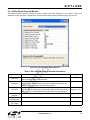
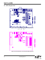
1
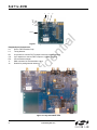
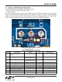
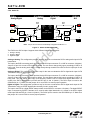
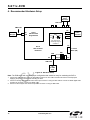
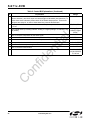
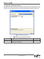
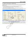
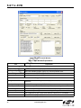
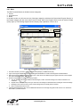
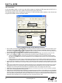
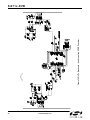
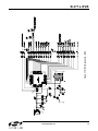
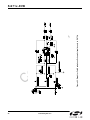
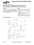
Si 4 7 1 x - EVB
S i471 X E V A L U A T I O N B O A R D U S E R ’ S G U I D E
1. Introduction
Thank you for purchasing the Silicon Laboratories Inc. Si471x FM Transmitter Evaluation Board (EVB). This EVB
and associated software has been designed to speed the overall development process and decrease the required
development time from EVB to product launch. We are looking forward to working with you, and have posted
support articles, answers to frequently asked questions, and application notes at www.mysilabs.com.
The Si471x EVB kit should include the following important items:
Si471x FM Transmitter customer welcome and evaluation letter
Si471x EVB baseboard Revision 1.3 (Firmware 1.B)
Si471x daughter card Rev 1.2 with Si471x chip pre-mounted
EVB characterization report
Si471x CD including:
Development application GUI
2. Overview
The Si471x Evaluation Kit includes an evaluation board (EVB) to facilitate evaluation of the Si471x using the
associated software. The EVB consists of a baseboard with a pre-mounted daughter card—Si471x is pre-installed
on the daughter card. The Si471x comes in a 3 x 3 mm 20-pin QFN package. Several input/output (I/O)
connections provide access to the various subsystems on the EVB. Refer to Figure 1 for the location of the various
I/O connectors/devices.
The Si471x family includes:
Si4710 - FM Transmitter
Si4711 - FM Transmitter with RDS
Si4712 - FM Transmitter with Received Power Scan (RPS)
Si4713 - FM Transmitter with RDS and RPS
This Firmware 1.B release supports Si471x with RDS and limiter as the new feature. On the Si47xx GUI itself, it
exposes the overmodulation, loud detection, and silence detection features that have been available from the
previous release.
This document references the Si471x data sheet.
Note: The Si471x Firmware 1.B uses library R4, which is not backwards compatible with the Si471x part that uses library R1
(e.g. Alpha 0, Alpha 1, Alpha 2, and Alpha 3).
3. Description
The following sections refer to both the image in Figure 1 and the silkscreen on the Si471x EVB. It is
recommended to refer to both when using this guide.
Preliminary Rev. 0.4 2/07
Copyright © 2007 by Silicon Laboratories
Silicon Laboratories Confidential. Information contained herein is covered under non-disclosure agreement (NDA).
Si471x-EVB
Si471x-EVB
J6
U10
J5/J13
J7
U9
J19
J27
J52
J30
J45
J44
J57
J41
X1
J61
J54
J68
J69
R73
R74
J75
J76
U18
D1
J79
J74
PB1 SW1 J78
Figure 1. Baseboard Connectors, Jumpers and Devices (Alpha 2)
Baseboard Power Connectors/Devices:
J79
USB connector (using USB power)
J78
External power connector
J76
Terminal block (TB) power connector
SW1 Switch to select between USB power or Ext power
R73
Potentiometer to adjust Vio voltage
R74
Potentiometer to adjust Vdd voltage
J61
J68
J69
2
Jumper: Baseboard power select (3.3 V or terminal block (TB))
Jumper: Si471x VIO power select (3.3 V or adjustable voltage via R73 or TB)
Jumper: Si471x VDD power select (3.3 V or adjustable voltage via R74 or TB)
Preliminary Rev. 0.4
Si471x-EVB
Baseboard Audio I/O Connectors/Devices:
J7
J6
J19
J30
U9
U10
RCA input
RCA output
Line/SPDIF input
Line/SPDIF output
S/PDIF Translator
CODEC
J5
J13
J41
J44
J45
Jumper: Analog audio right channel select (RCA or Line In)
Jumper: Analog audio left channel select (RCA or Line In)
Jumper: For GPO3/DCLK pin, select between GPO3 or DCLK
Jumper: Si471x Audio1 select (Transmit or Receive)
Jumper: Si471x Audio 2 select (Transmit or Receive)
Baseboard Clock Connectors/Devices:
X1
32.768 kHz crystal oscillator
J52
Jumper: select Int RCLK or Ext RCLK
J54
Ext RCLK SMA connector input
J57
Jumper: disable Int RCLK
Baseboard MCU Connectors/Devices:
U18
C8051F342 MCU
J79
USB connector to communicate with the MCU
J74
JTAG connector for the MCU
PB1
Push button to reset the MCU
D1
LED to confirm power supply to the MCU
Baseboard to Daughter Board Connectors:
J27
Si471x daughter card connector
J75
Expansion card connector (reserved)
Preliminary Rev. 0.4
3
Si471x-EVB
J1
L2
U1
R4
C8
R2
J2
Antenna
Figure 2. Daughterboard Connectors and Devices
Daughterboard Components:
U1
Si471x FM Transmitter Chip
L2
Tuning Inductor
R2
0 Ω resistor to connect FM TX output to 6cm trace built-in antenna
C8
2 pF capacitor to connect FM TX output to J1 SMA connector
R4
50 Ω terminator resistor
J1
J2
SMA connector for FM transmitter output
Header for putting external antenna
Figure 3. Fully Assembled EVB
4
Preliminary Rev. 0.4
Si471x-EVB
3.1. Jumper or Solder Bump Configuration
The EVB for the Si471x has two different ways to setup jumpers:
1. Berg stick jumper (if the Bergstick headers are installed).
2. Solder bump jumper.
If you have an EVB that doesn't have the header installed, then use the solder bump jumper to select the desired
settings. The solder bumps and Bergstick jumpers exist in parallel, so only use one of them. If using the Bergstick
jumpers, then remove solder from the solder bumps associated with live Bergstick jumpers. If using the solder
bumps, then please make sure there are no jumpers placed on the associated Bergstick jumpers.
Figure 4. Solder Bump Jumper (circled)
Table 1. EVB Configuration Matrix
Jumper
Description
Choices
Type
Default Setting
J61
Select baseboard power
source
+3.3 V/terminal block
Jumper
+3.3 V
J68
Select Vio power source
+3.3 V/terminal
block/adjustable via R73
Jumper
+3.3 V
J69
Select Vdd power source
+3.3 V/terminal
block/adjustable via R74
Jumper
+3.3 V
J15
Select analog audio in
RCA in/Line in
Jumper
RCA In
J31
Select analog audio in
RCA in/Line in
Jumper
RCA In
J41
Select GPO3 connection
GPIO3/DCLK
Jumper
GPIO3
J44
Select audio 1 configuration
TX/RX
Jumper
RX
J45
Select audio 2 configuration
TX/RX
Jumper
TX
J52
Select RClk source
Int RCLK/Ext RClk
Solder bump
Int RClk
J57
Disable Int RClk
Enable/Disable
Jumper
unconnected (Enable)
Preliminary Rev. 0.4
5
Si471x-EVB
3.2. Si471x Base Board
3.2.1. Power Supply Network
DAUGHTER BOARD
SW1
LDO
1.25-3.9V
(R73)
J78
EXT
LDO
1.25-7V
(R74)
ADJ
Jumper
J69
+3.3V
11 VDD
VIO
TB +3.3V
J79
USB
ADJ
Jumper
J68
10
TB
LDO
+3.3V
(U17)
Si471x
TB
Jumper
J61
+3.3V
Vmcu
VIO
Vm
Vio
Vdd
Gnd
VDD
J77
Terminal
Block (TB)
Figure 5. Power Supply Block Diagram
The EVB can be powered from 3 different kinds of power supplies:
1. USB power supply via J79
2. Ext DC power supply via power jack J78
3. Three separate power supplies (Vdd, Vio, Vmcu) via terminal block J76
The EVB has three different rails: Vdd, Vio, and Vmcu. Vdd and Vio are routed directly to the daughter board to
power the Vdd and Vio pins on the Si471x chip, while Vmcu is used to power the entire base board.
USB Power Supply & EXT DC Power Supply
Switch SW1 is used to select between the USB supply and Ext DC supply.
There are 2 modes that the user can use with the USB or the EXT DC supply:
1. Fixed +3.3 V
2. Adjustable Vdd and Vio
6
Preliminary Rev. 0.4
Si471x-EVB
Fixed +3.3V
ADJ
+3.3V
TB
J68
J69
Vmcu
+3.3V
Vdd
TB
Vio
ADJ
+3.3V
TB
Only one LDO is being used in this mode which outputs a +3.3 V supply to all three Vdd, Vio, and Vmcu supplies.
The jumpers need to be set according to Figure 6. This is the default configuration of the EVB.
J61
Figure 6. Default Fixed +3.3 V Jumpers Setting
Adjustable Vdd and Vio
ADJ
+3.3V
TB
J68
J69
Vmcu
+3.3V
Vdd
TB
Vio
ADJ
+3.3V
TB
In case Vdd and Vio supplies to the Si471x chip need to be adjusted or swept, two adjustable LDOs have been put
on the EVB. The Vio supply can be adjusted via potentiometer R73, while Vdd supply via R74. The jumpers need
to be set according to Figure 7.
J61
Figure 7. Adjustable Vdd and Vio Jumpers Setting
Terminal Block Power Supply
ADJ
+3.3V
TB
J68
J69
Vmcu
+3.3V
Vdd
TB
Vio
ADJ
+3.3V
TB
If the terminal block supplies are used, then jumpers J61, J68 and J69 need to be set to TB according to Figure 8.
The user then needs to connect three different power supplies, one each for Vdd, Vio and Vmcu.
J61
Figure 8. Terminal Block Jumpers Setting
Preliminary Rev. 0.4
7
Si471x-EVB
3.2.2. Microcontroller
TC_BCLK
(for digital tx/rx make
sure to connect this)
Jumper
J41
DAUGHTER BOARD
MD_GPIO3
MS_GPIO2
MD_GPIO1
J79
USB
J74
JTAG
SD_GPO1
GPO1
GPO2
GPO3/
DCLK
Jumper
J65
MCU
C8051F342
PB1
Reset
S_GPO3/DCLK
MD_GP4
MS_RSTB
19 18 17
RST~ 5
Si471x
SEN~
SCLK
SDIO
6 7 8
MS_SENB
MS_SCLK
MS_SDIO
Figure 9. MCU Block Diagram
The Si471x evaluation environment uses a Silicon Laboratories' C8051F342 microcontroller to control the Si471x
and to provide USB connectivity to the EVB (via J79). The LED D1 illuminates to confirm that power is being
properly supplied to the C8051F342 and that firmware has been loaded. Push-button PB1 manually resets the
C8051F342. The JTAG connector J74 is used to program the C8051F342 at production time, and is not necessary
for further development.
8
Preliminary Rev. 0.4
Si471x-EVB
3.2.3. Reference Clock for the Si471x
DAUGHTER BOARD
Jumper
J57
DIS_INT_RCLK
X1
32.768kHz
INT RClk
Si471x
INT_RCLK
Jumper
J52
9
RCLK
EXT_RCLK
J54
EXT
RClk
Figure 10. Reference Clock Block Diagram
The Si471x accepts a 32.768 kHz reference clock at the RCLK pin. On the EVB, this clock is provided by a
precision crystal oscillator. The user has the option of not using the oscillator and bringing in the reference clock
from an external source through SMA connector J54.
When the user chooses to provide an external RCLK jumper J52 has to be set accordingly. Also the user has the
option to turn off the onboard crystal oscillator by installing jumper J57.
Preliminary Rev. 0.4
9
Si471x-EVB
3.2.4. Audio I/O
EVB In
Analog/Digital
471x Audio2
Analog
Audio2
Select
J7
RCA In
Jumper
J5&J13
AUDIO2
DOUT
0
AUDIO1:
Digital TX
DFS1 14
DIO1 13
SI471x
(daughter board)
CODEC IN
LINE
IN
S/PDIF IN
J6
RCA Out
0
0
1
1
CODEC OUT
AUDIO1
To_TX
1
J19
SPDIF In
(white)
16 LIN
15 RIN
0
EVB Out
N/A
Audio1
Select
AUDIO2:
Analog TX
1
J19
Line In
(white)
471x Audio1
Digital
J30
Line Out
(black)
LINE
OUT
DIN
From_RX
Jumper
J45
From_RX
To_TX
SPDIF
DOUT
IN
Jumper
J44
S/PDIF OUT
DIN
SPDIF
OUT
J30
SPDIF Out
(black)
Digital Input
Select
Note: Jumper J44 and J45 are automatically configured in EVB Rev 1.3.
Figure 11. Audio I/O Block Diagram
The EVB for the Si471x Alpha 3 supports three different kinds of configurations:
1. Analog to Analog
2. Analog to Digital
3. Digital to Digital
Analog to Analog: This configuration provides a way for the user to evaluate the Si471x analog audio input for FM
transmission.
The input to the EVB is an analog audio provided via the RCA input connector J7 or LINE In connector J19 (white).
Jumpers J5 and J13 are set to RCA input by default. The user has to change this jumper accordingly if LINE In is
being used. Then the analog audio input is routed directly through a switch to the Si471x Rin/Lin inputs pin 15 and
16 (Audio2).
Analog to Digital: This configuration provides a way for the user to evaluate the Si471x digital audio input for FM
Transmission using an analog audio input.
The input to the EVB is an analog audio provided via the RCA input connector J7 or LINE In connector J19 (white).
Jumpers J5 and J13 are set to RCA input by default. The user has to change this jumper accordingly if LINE In is
being used. Then the analog audio input is converted by CODEC U10 to a serial audio digital data before it is
routed to the Si471x digital audio input DIO and DFS pin 13 and 14 (Audio1). The DCLK input is routed to the
GPO3/DCLK pin 17. Make sure that jumper J41 is set to DCLK to ensure proper operation.
Digital to Digital: This configuration provides a way for the user to evaluate the Si471x digital audio input for FM
Transmission using an S/PDIF digital audio commonly found in sound cards.
The input to the EVB is a digital S/PDIF data provided via the S/PDIF In connector J19 (white). The digital S/PDIF
input is converted by S/PDIF Translator U9 to a serial audio digital data before it is routed to the Si471x digital
audio input DIO and DFS pin 13 and 14 (Audio1). The DCLK input is routed to the GPO3/DCLK pin 17. Make sure
that jumper J41 is set to DCLK to ensure proper operation.
10
Preliminary Rev. 0.4
Si471x-EVB
IMPORTANT: Jumper Settings
Because of the many possibilities available to configure the EVB, please make sure that these four jumpers are set
accordingly:
1.
2.
3.
4.
J41: GPO3/DCLK setting
J44: TX/RX setting for Audio1 I/O
J45: TX/RX setting for Audio2 I/O
J5– J13: Analog Audio Source, RCA or Line In
J41: GPO3/DCLK Setting
Upper - DCLK digital audio clock
Lower - GPO3 digital control signal
For configuring the Si471x digital audio input, make
sure that the jumper is set in the Upper position so that the DCLK signal will be routed to the Si471x.
J44: TX/RX setting for Audio1 I/O
Upper - Audio1 is set to FM transmit (pin 13&14 will be the digital audio input).
Lower - Audio1 is set for FM receive (pin 13&14 will be analog/digital audio output).
J45: TX/RX setting for Audio2 I/O
Upper - Audio2 is set to FM transmit (pin 15&16 will be the analog/digital audio input).
Lower - Audio2 is set for FM receive (pin 15&16 will be the digital audio output).
Please refer to the jumper setting instructions found in the Si471x GUI software when configuring the board.
J5–J13: Analog Audio Source, RCA or Line In
Upper - RCA inputs are used for analog audio source.
Lower - Line inputs are used for analog audio source
3.3. Si471x Daughter Card
3.3.1. Si471x FM Transmitter Chip
The Si471x (U1) and its bypass capacitors and tuning inductor (L2) are located on the daughter card. The FM
Transmit output can be configured in three different ways:
1. Built-in antenna
2. External antenna
3. RF output
Built-in Antenna
To use the 6 cm trace built-in antenna, please make sure to put a 0ohm resistor in R2 and remove R3 resistor.
External Antenna
To use an external antenna, please remove both R2 and R3 resistors. Put the external antenna in the J2 header
connector.
Rf Output
To analyze the performance of the Si471x FM Transmitter Output, please put a 0ohm resistor in R3 and remove R2
resistor. The FM RF output will be available through the SMA connector J1.
Refer to “AN306: Antenna Interface" for a more complete study of the antenna interface for the Si471x.
Preliminary Rev. 0.4
11
Si471x-EVB
4. Recommended Hardware Setup
Analog
Audio
Generator
RCA Cable
J7
RCA IN
SMA Cable
RF
Analyzer
J1
FM
OUT
J19
Si471x
FM Transmitter
Daughterboard
Jumpers
Setting
DCLK
TX
GPIO3
J41
RX
RX
J44 J45
S/PDIF
Audio
Generator
TX
Note: J44 and J45 are
automatically configured
in EVB Rev1.3
J76
Si471x
FM Transmitter
Baseboard
Terminal
Block (TB)
USB
J79
SW1
EXT pwr
USB pwr
J77
EXT Jack
USB Cable
PC
w/ USB
port
Figure 12. Hardware Setup
Note: The EVB comes with a default jumper configuration that should be ready for evaluating the Si471x.
1. Connect the USB cable from PC to the EVB USB connector J79. The USB connection will serve as a dual purpose:
supplying the power to the EVB and controlling the EVB.
2. Connect an analog audio generator to the RCA input connector J7 using an RCA cable or connect an SPDIF digital audio
generator to connector J19 using an SPDIF cable.
3. Connect an RF analyzer from the FM output SMA connector J1 using an SMA cable.
12
Preliminary Rev. 0.4
Si471x-EVB
5. Getting Started - Software Installation (Firmware 1.B)
The Si471x Windows GUI (graphical user interface) Software is designed and intended for use only with the Si471x
evaluation board (EVB). This user guide is written to support Firmware Revision 1.B. The GUI software revision
number is available under help\about.
The GUI software development program uses host machine USB port to communicate with the Si471x EVB and is
tested for use with Windows XP and Windows 2000.
Note: If you have installed previous version of the GUI, please make sure that:
1. The old version is removed.
2. The Si47xx GUI folder located in “C:\Program Files\Silcon Laboratories Inc” is deleted.
Failure to remove the old version and its folder will cause Si47xx GUI to not function properly.
Below is a couple of screen shots illustrating how to remove the old Si471xx GUI and its folder.
Figure 13. Si47xx GUI Removal
Preliminary Rev. 0.4
13
Si471x-EVB
Figure 14. Delete the Si47xx Folder Entirely
After the old version has been removed, insert the Silicon Laboratories, Inc. Si471x CD into the host machine CD
drive and launch Windows Explorer. Open the CD to explore the contents in a window like the one shown in
Figure 15.
Figure 15. Installation and Setup Start Screen
Important: Open and read the ReleaseNotes.txt file at this point. It may contain information that is not captured
here, and which could be very important to the functionality of the EVB or Software.
Run the Setup.Exe and follow the instructions on the screen.
Note: If you get this Error message: "This setup requires the .NET Framework version [1]"; then you should install
the .NET Framework that is provided on the CD and re-run the setup.
After installation is finished, an Si47XXGui icon will appear on your desktop. Launch the software by clicking this is
icon on the desktop as shown in Figure 16.
14
Preliminary Rev. 0.4
Si471x-EVB
Figure 16. Launching Si471x FM Transmitter Application
The first Si471x window is the Initialization window as shown in Figure 19. Select the target device by clicking on
the EVB serial number with the Si471x name underneath. Click open, and a new window displaying "Initializing
Transmitter" will appear. There are three modes to configure the Si471x with the Alpha 3 release:
1. Analog Input
2. Analog to Digital Input
3. Digital Input
Preliminary Rev. 0.4
15
Si471x-EVB
5.1. Configuring the Si471x to Receive Analog Input
This mode configures the Si471x to receive analog audio input at pin 15 and 16 (LIN and RIN). The user has the
ability to provide analog audio from RCA In connector (J7) or Line In (J19). Please set jumpers J5 and J13
accordingly. Figure 17 shows the configuration setting for analog audio input.
Figure 17. Configuring Si471x to Receive Analog Input
16
Preliminary Rev. 0.4
Si471x-EVB
5.2. Configuring the Si471x to Receive Digital Input by Using Analog Source
This mode configures the Si471x to receive digital audio input at pin 13 and 14 (DIN and DFS), but the user still
provides an analog audio source to the EVB. It is useful for a user who wants to test digital input on the Si471x but
does not have a digital audio source. The analog audio source is converted to digital audio through the CODEC,
which can be configured to output various digital audio formats. Please refer to Figure 23, “CODEC Property
Window,” on page 25 to control the CODEC.
Note: Please set jumper J41, J44, and J45 according to Figure 18 to properly operate in digital mode.
Figure 18. Configuring Si471x to Receive Digital Input by Using Analog Source
Preliminary Rev. 0.4
17
Si471x-EVB
5.3. Configuring the Si471x to Receive Digital Input by Using Digital Source (SPDIF)
This mode configures the Si471x to receive digital audio input at pin 13 and 14 (DIN and DFS) when the user has
an SPDIF digital audio source. The SPDIF source is converted to PCM digital audio by the SPDIF translator.
Please refer to Figure 24, “SPDIF Property Window,” on page 26 to control the SPDIF translator.
Notes: - Please set jumper J41, J44, and J45 according to Figure 19 to properly operate in digital mode.
- The Si471x requires the digital audio signal to be present when initializing the part. Therefore, please
connect the SPDIF IN signal prior to initializing the part.
Figure 19. Configuring Si471x to Receive Digital Input by Using Digital Source (SPDIF)
TIP. If the Si471x Development GUI doesn't find your device, try unplugging and plugging in the USB cable again.
18
Preliminary Rev. 0.4
Si471x-EVB
6. Development Using Si471x GUI (Firmware 1.B)
6.1. Si47xx GUI - Main Window
1
2
3
15
16
4
17
5
9
6
10
7
12
8
13
18
19
11
20
21
22
14
23
Figure 20. Si471x FM Transmitter Window
Table 2. Control Bit Explanations
#
Explanation
Range
1 Transmit frequency display. Enter the desired FM transmit frequency in this window.
76–108 MHz
2 Transmit power display. Enter the desired FM transmit power in this window.
88–120 dBuV
3 RF on or off. Turning this button on will enable the FM transmit, while turning this button
off will disable the FM transmit.
On/Off
4 Varactor Value. This is an indicator showing the tuning cap value of the Si471x chip.
Each number represents 0.25 pF. If the varactor value is manually overwritten in the
property window, the indicator will change from automatic mode to manual mode.
1–191
5 Audio Deviation. Enter the desired audio deviation in this window.
0–90 kHz
6 Pilot Deviation. Enter the desired pilot deviation in this window.
0–90 kHz
7 RDS Deviation. Enter the desired RDS deviation in this window (Si4711/13 only).
0–7.5 kHz
8 Total Deviation. This is an indicator only displaying the sum of the audio, pilot and RDS
deviation. If the total deviation exceeds 75 kHz, the indicator will turn red and a warning
sign is displayed.
0–187.5 kHz
9 Input Mute Left/Right. Turning this button will mute the Left or Right audio channel.
On/Off
10 Turn on or off the pilot tone for stereo or mono FM transmit mode.
On/Off
11 Turn on or off the L-R channel for stereo or mono FM transmit mode.
On/Off
12 Turn on or off the RDS transmission (Si4711/13 only).
On/Off
13 Modulation On. Clicking this button on will modulate the audio, pilot, and RDS signal
according to the audio, pilot, and RDS deviation. Turning this button off will turn off modulation for all audio, pilot, and RDS signal.
On/Off
Preliminary Rev. 0.4
19
Si471x-EVB
Table 2. Control Bit Explanations (Continued)
#
Explanation
Range
14 Audio Level Indicators: Overmodulation, Audio input level below low-level threshold
(silence detection), and Audio input level below high-level threshold (loud detection). To
enable these three indicators please check off the Enable Interrupts box. These three
indicators are sticky bit, in order to clear these bits, press the Reset button.
—
15 Pre-Emphasis. Click one of the three buttons to set the pre-emphasis either to Off, 50 us
or 75 us.
Off, 50 us, 75 us
16 Si471x EVB audio input setting indicator: Analog In / Digital (Analog In to CODEC) / Digital (SPDIF)
Analog, Digital
CODEC, Digital
SPDIF
17 Turn on or off the compressor for the audio signal
18 Attack time. Set the attack time for the compressor in millisecond
On/Off
0.5–5 ms
19 Release time. Set the release time for the compressor in millisecond
100–1000 ms
20 Threshold. Set the threshold for the compressor
–40 to 0 dBFS
21 Input Gain. Set the compressor gain.
0 to 20 dB
22 Turn on or off the limiter feature
On/Off
23 Set the limiter release time constant
20
0.5,1,2,3,4,5,6,7,8,
9,10,20,30,40,50,
75,100 ms
Preliminary Rev. 0.4
Si471x-EVB
6.2. Si47xx GUI - Analog Property Window
This Analog Property Window controls the various analog audio input properties on the Si471x. Clicking on
Windows→Properties when in Analog Mode will launch the Analog Property Window as shown in Figure 21.
Figure 21. Si471x Analog Property Window
Table 3. Analog Property Window Explanations
Item
Explanation
GUI Update Rate Set the GUI update rate between the computer and the EVB.
(Sec)
Range
0.2–10 Sec
Reference Clock This is the internal Reference Clock Frequency on the chip and it is calcuFrequency
lated by dividing RCLK by the prescaler.
31130–34406 Hz
Reference Clock Reference Clock Prescaler allow the user to have an RCLK from 32 kHz to
Prescaler
40 MHz. Any RCLK that the user supplies should be divided by this prescaler to get as close to 32.768 kHz as possible.
1–4095
Varactor Capaci- This field allows the user to manually overwrite the tuning capacitance. 0
tor Overwrite
indicates that the tuning cap is automatically adjusted. Any number other
than 0 (1 to 191) will indicate that the tuning cap is manually adjusted.
automatic: 0,
manual: 1–191
Audio Level Low Set the threshold in which an interrupt will be generated when the audio
Threshold (dBFS) input level falls below this threshold for the duration greater than the Audio
Level Low Distortion setting. This may be called silence detection indicator
–70 to 0
Audio Level Low Set the duration for the audio level low before an interrupt is generated.
Duration (mSec)
0–65535
Preliminary Rev. 0.4
21
Si471x-EVB
Table 3. Analog Property Window Explanations (Continued)
Item
Explanation
Range
Audio Level High Set the threshold in which an interrupt will be generated when the audio
Threshold (dBFS) input level rises above this threshold for the duration greater than the Audio
Level High Duration setting. This may also be called loud detection indicator.
–70 to 0
Audio Level High Set the duration for the audio level high before an interrupt is generated.
Duration (mSec)
0–65535
Line Input
Attenuation
The Si471x chip has 4 attenuator setting (636, 416, 301, and 190 mVp). It
will tell the maximum audio input signal that the user can give to the LIN and
RIN input. The attenuator setting will determine the audio input impedance
(LIN and RIN) of the chip.
190 mVp,
301 mVpk,
416 mVp,
636 mVpk
Maximum Line
Input Level
The maximum line input level is like a fine adjustment of the max audio input
signal that the user supply to the chip. This number has to be less than or
equal to the attenuation setting. The max line input level will correspond to
the max audio deviation set in the audio deviation window on the main GUI.
Make sure that the actual audio input signal does not exceed this limit, otherwise the audio signal will become distorted.
0–636 mVpk
22
Preliminary Rev. 0.4
Si471x-EVB
6.3. Si47xx Digital Property Window
This Digital Property Window controls the various digital audio input properties on the Si471x. Clicking on
Windows→Properties when in Digital Mode will launch the Digital Property Window as shown in Figure 22.
Figure 22. Si471x Digital Property Window
Table 4. Si471x Digital Property Window Explanations
Item
Explanation
Range
Reference Clock
Frequency
This is the internal Reference Clock Frequency on the chip and it is calcu- 31130–34406 Hz
lated by dividing RCLK by the prescaler.
Reference Clock
Prescaler
Reference Clock Prescaler allow the user to have an RCLK from 32 kHz
to 40 MHz. Any RCLK that the user supplies should be divided by this
prescaler to get as close to 32.768 kHz as possible.
Varactor Capacitor This field allows the user to manually overwrite the tuning capacitance. 0
Overwrite
indicates that the tuning cap is automatically adjusted. Any number other
than 0 (1 to 191) will indicate that the tuning cap is manually adjusted.
1–4095
automatic: 0,
manual: 1–191
Digital Sample
Precision
Select the precision of the digital audio input
Digital Mono
Mode Enable
Select between Digital Stereo or Mono
On/Off
Digital Swap
Left - Right
Select whether the DIN L-R data is normal or swapped
On/Off
Preliminary Rev. 0.4
8, 16, 20, 24 bits
23
Si471x-EVB
Table 4. Si471x Digital Property Window Explanations (Continued)
Item
Explanation
Range
Digital DFS
Inversion Enable
Select whether the DFS Frame Clock is normal or inverted
On/Off
Digital DFS
Late Mode
Select PCM digital audio data between I2S or Left Justified
On: Left-Justified,
Off: I2S
Digital DFS
Pulse Mode
Select between using a regular 50% duty cycle Frame Clock, or a Pulse
Frame Clock
On/Off
Digital DCLK
Falling Edge
Select between using rising edge or falling edge of DCLK when sampling
Digital Input (DIN) data
On/Off
24
Preliminary Rev. 0.4
Si471x-EVB
6.4. Si47xx GUI - CODEC Property Window
This CODEC Property Window controls the various properties of the CODEC on the EVB baseboard. In the Digital
Mode, when using the Analog In to CODEC method, the Digital Property Window has a baseboard setting that can
be selected in the property category pull-down menu where the window will become the CODEC Property Window.
Figure 23. CODEC Property Window
Table 5. CODEC Property Window Explanations
Item
CODEC Precision
Explanation
Range
16, 20, 24 bits
Select the CODEC digital audio output precision
CODEC Output Format Select the CODEC digital audio format between I S or Left Justified Left-Justified or I2S
2
CODEC Sampling Rate Select the precision of the CODEC digital audio output
CODEC Channel Swap Select whether the CODEC digital output L-R data is normal or
swapped
CODEC Invert Clock
Select between using rising edge or falling edge of DCLK when sampling Digital Input (DIN) data
Preliminary Rev. 0.4
32 or 48 kHz
On / Off
On / Off
25
Si471x-EVB
6.5. Si47xx GUI - SPDIF Property Window
This SPDIF Property Window controls the various properties of the SPDIF translator on the EVB baseboard. In the
Digital Mode, when using the SPDIF method, the Digital Property Window has a baseboard setting that can be
selected in the property category pull-down menu where the window will become the SPDIF Property Window.
Figure 24. SPDIF Property Window
Table 6. SPDIF Property Window Explanations
Item
Explanation
SPDIF Output Format Select the SPDIF digital audio format between
SPDIF Invert Clock
26
Range
I2S
or Left Justified
Select between using rising edge or falling edge of DCLK when
sampling Digital Input (DIN) data
Preliminary Rev. 0.4
Left-Justified or I2S
On / Off
Si471x-EVB
6.6. Si47xx GUI - Register Map Window
The register map window allows the user to manually program the device by sending commands to the chip. Refer
to “AN305: Si4710/11 FM Transmitter Programming Guide” to be able to manually program the device. Clicking on
Windows→Register Map will launch the Register Map Window as shown in Figure 25.
Figure 25. Si471x Register Map Window
Preliminary Rev. 0.4
27
Si471x-EVB
6.7. Si47xx GUI - Received Power Scan Window
The Received Power Scan Window is only available with the Si4712/13 devices. It enables the user to scan the
entire FM band to find an empty channel. The frequency of this channel can then be used to transmit. Clicking on
Windows→Power Scan will launch the Received Power Scan Window as shown in Figure 26
Figure 26. Si4712/13 Received Power Scan Window
28
Preliminary Rev. 0.4
Si471x-EVB
6.8. Si47xx GUI - Radio Data Service (RDS) Window
The RDS/RBDS feature is only available in the Si4711/13 part and the Si47xx GUI allows user to evaluate the
RDS/RBDS transmission on these parts. This user guide assumes that the user is already familiar with the
RDS/RBDS standard.
User may refer to the following documents if needs to be familiar with the RDS/RBDS standard:
1. United States RBDS Standard by National Radio Systems Committee, April 9, 1998.
2. RDS Universal Encoded Communication Protocol Version 5.1 by European Broadcasting Union, August 1997.
3. Silicon Labs AN243: Using RDS/RBDS with the Si4701/03
In order for the user to transmit RDS please check the RDS On box. Failure to turn on RDS means that the RDS
data will not be transmitted. The following picture illustrated the RDS On box that should be turned on.
Figure 27. Turning on RDS in the Main GUI Window
After the RDS transmission is enabled, click on Window -> RDS Transmit Data to go to the RDS Transmit Data
screen. This window allows the user to play around with what kind of RDS data will be transmitted and also allows
the user to gain insight to the Si471x RDS capability.
Preliminary Rev. 0.4
29
Si471x-EVB
Figure 28. RDS Transmit Window
Table 7. RDS Window Explanations
Item
Explanation
General
RDS / RBDS Selection
Program Type (PTY)
PTY Dynamic
PI
Select either RDS format (Europe) or RBDS format (US).
Select the available Program Type (PTY) from the pulldown menu.
Select whether the PTY will be dynamic or static.
Enter Program Identification (PI) code here.
Program Service
Program Service Boxes
Load Messages
Load the PS messages to the Si4711/13 chip.
Repeat Count
Enter how many time each PS will be repeated before sending the next PS.
Message Count
Enter how many messages of the loaded PS that will actually be transmitted.
Mix
30
Enter up to 12 different Program Service (PS). Each PS consists of a maximum 8
characters.
Select the mix percentage between transmitting the Program Service or Buffers.
Alternate Frequency
Part of RDS Group Type 0 (PS): Enter Alternate Frequency if it is available.
Artificial Head
Part of RDS Group Type 0 (PS): Enter whether Artificial Head is On or Off.
Preliminary Rev. 0.4
Si471x-EVB
Table 7. RDS Window Explanations
Item
Stereo
Audio Compression
Explanation
Part of RDS Group Type 0 (PS): Enter whether the transmitted audio is Stereo or
Mono.
Part of RDS Group Type 0 (PS): Enter whether the Audio Compression is On or Off.
Traffic Program
Part of RDS Group Type 0 (PS): Enter whether Traffic Program is available or not.
Traffic Announcement
Part of RDS Group Type 0 (PS): Enter whether Traffic Announcement is available or
not.
Speech
Part of RDS Group Type 0 (PS): Enter between Speech or Music transmission.
Buffers
Radio Text
Radio Text: A/B Flag
Enter the RDS Group Type 2 Radio Text (RT) messages that will be uploaded to
either the circular or FIFO buffer.
Part of RDS Group Type 2 (RT): Enter whether the A/B Flag is set or not in entering
the RT. This A/B Flag will tell the receiver to clear the display when the flag toggles
from one state to the other.
Radio Text: Add to Circular Add the RT messages that are typed into the circular buffers.
Radio Text: Add to FIFO
Add the RT messages that are typed into the FIFO buffers.
Manual Group Entry: B
Enter manual RDS entry block B. With this window you can practically transmit all
RDS Group Type 0 through 15.
Manual Group Entry: C
Enter manual RDS entry block C. With this window you can practically transmit all
RDS Group Type 0 through 15.
Manual Group Entry: D
Enter manual RDS entry block D. With this window you can practically transmit all
RDS Group Type 0 through 15.
Manual Group Entry: Add to Add the RDS manual entry into the circular buffers.
Circular
Manual Group Entry: Add to Add the RDS manual entry into the circular buffer.
FIFO
Circular
Indicator showing the data that will be sent to the circular buffers.
Circular: Size (Blocks)
Indicator showing the size (in blocks) of the circular buffer. The total size of the
buffer is 128 which is shared between the circular and FIFO buffers. To adjust the
size, please change the size in the FIFO buffers.
Circular: Delete Group
Delete a group that is selected in the Circular Indicator window.
Circular: Clear Buffer & Send Clear the data that is currently in the circular buffer and load it with the new one that
is displayed in the circular indicator window.
FIFO
Indicator showing the data that will be sent to the FIFO buffers.
FIFO: Size (Blocks)
Indicator showing the size (in blocks) of the FIFO buffer. Adjusting the size of the
FIFO, will also adjust the size of the circular buffer. The total of those two buffers are
128 blocks.
FIFO: Add Time
This will get the current time and format it into RDS Group Type 4 Clock & Time
(CT), sent to the FIFO indicator window and have it ready to be loaded into the FIFO
buffers.
FIFO: Delete Group
Delete a group that is selected in the FIFO Indicator window.
FIFO: Clear Buffer & Send Clear the data that is currently in the FIFO buffer and load it with the new one that is
displayed in the FIFO indicator window.
Preliminary Rev. 0.4
31
Si471x-EVB
There are 16 different group types in the RDS/RBDS standard, and for every group the following information is
always transmitted:
1. Program Identification (PI)
2. Program Type (PTY)
The Si47xx GUI makes it easy to send data in 3 of the following group types:
1. Group Type 0: Program Service (PS)
2. Group Type 2: Radio Text (RT)
3. Group Type 4: Clock Time (CT)
It is possible to send data in the other group types, but the user has to manually enter the data in hexadecimal
code.
Because of the complexity of the RDS/RBDS standard, the explanation of the RDS Transmit Data window is
divided into three sections: Basic, Intermediate, and Advanced.
32
Preliminary Rev. 0.4
Si471x-EVB
6.8.1. Basic
The RDS Transmit Window is divided into three categories:
1. General
2. Program Service
3. Buffers
In the basic section, we will cover two out of the three categories, which are the General and Program Service. In
the General category the user can set the PI and PTY data, while in the Program Service user will set the PS data
(Group Type 0). The following diagram shows a step-by-step explanation of how to do it:
1
3
2
4
5
Figure 29. Basic RDS Sending Message Illustration
1. First select whether you want to transmit in RDS format (Europe) or RBDS format (US)
2. Type in the Program Identification in this field. Program Identification is a 16bit code assigned to individual station.
3. Select the Program Type in the pulldown menu here. There are a lot of different program types and some of the examples
are: news, information, sports, talk, rock, etc.
4. Enter the Program Service (PS) in the boxes provided:
a. You can enter a maximum of 12 different PS messages, in which each PS message can contain a maximum of 8
characters.
b. Repeat Count: Enter how many times you want each PS message is transmitted before sending the next PS message.
c. Message Count: Enter how many of the 12 PS message that you actually want to transmit.
d. Mix: Put 100 percent here for now.
5. Click Send Message button here. Now the RDS will transmit the PS message along with the PI and PTY. You should see
these data in your RDS receiver.
Preliminary Rev. 0.4
33
Si471x-EVB
6.8.2. Intermediate
In the intermediate section, we will cover the buffers category of sending the RDS data with the Si4711/13, in
particular we will send Group Type 2 (Radio Text) and Group Type 4 (Clock Time).
The following diagram shows a step-by-step procedure to send the buffers data in addition to the General and
Program Service data covered in the basic section.
1
2
3a
3
5
6
4
Figure 30. Intermediate RDS Sending Message Illustration
1. Select the Mix percentage that you want between transmitting the data in Program Service and the data in the Buffers. 100%
means that you will always transmit the PS message regardless of what is contained in the Buffers, while 0% means that
you will always transmit the data in the Buffers regardless of what is contained in the PS. If the buffers are empty though, the
PS messages will be transmitted all the time regardless of the mix percentage.
2. Enter the Radio Text message that will be transmitted. After entering the RT message, click either the "Add to Circular"
button or the "Add to FIFO" button. The RT message will be encoded according to the RDS Group Type 2 rule.
a. Clicking "Add to Circular" button means that you upload the RT message into the Circular Buffer Indicator Window.
Note that the message itself has not been uploaded into the Circular Buffer inside the Si4711/13 until the Clear Buff &
Send is clicked.
b. Clicking "Add to FIFO" means that you upload the RT message into the FIFO Buffer Indicator Window. Note that the
message itself has not been uploaded into the FIFO Buffer inside the Si4711/13 until the Clear Buff & Send is clicked.
3. Enter the size of the FIFO that you want here. The Si4711/13 buffer has a total of 128 blocks, which is shared by the circular
buffer and the FIFO. Therefore the circular buffer size (shown in 3a) will be the remainder of the 128 blocks minus the FIFO
size.
4. Clicking this "Clear Buff & Send" button will upload the message from the Circular Buffer Indicator Window into the Circular
Buffer inside the Si4711/13. Circular buffer holds the message that will be transmitted over and over again. Note that the
messages in the circular buffer will be transmitted only if the PS Mix value is set to anything other than 100%.
5. Clicking the "Add Time" button here will automatically upload the current time into the FIFO. The CT time data is uploaded
into the Si4711 according the RDS Group Type 4 rule.
6. Clicking the "Clear Buff & Send" button will upload the message from the FIFO Buffer Indicator Window into the FIFO Buffer
inside the Si4711/13. FIFO buffer holds the message that will be transmitted only once. A good example of using FIFO buffer
is when you want to send the time data. Time is something that occurs only once, so it will not be beneficial to upload time to
the circular buffer and get transmitted continuously. We will cover how to send time in step #5. Note that the messages in the
FIFO buffer will be transmitted only if the PS Mix value is set to anything other than 100%.
34
Preliminary Rev. 0.4
Si471x-EVB
6.8.3. Advanced
1
2
3
4
5
6
8
7
9
Figure 31. Advanced RDS Sending Message Illustration
1. Dynamic: This tells whether the PTY code is static or dynamic.
2. Alternate Frequency: This provides the ability to inform the receiver of a single alternate frequency. This field is transmitted
along with the Group Type 0 (PS).
3. Miscellaneous bits in Group Type 0 (PS):
a. Artificial Head: 0 = Not Artificial Head, 1 = Artificial Head
b. Stereo: 0 = Mono, 1 = Stereo
c. Audio Compressor: 0 = Not compressed, 1 = Compressed
d. Traffic Program (TP): 0 = No TP, 1 = TP
e. Traffic Announcement (TA): 0 = No TA, 1 = TA
f.
Speech: 0 = Speech, 1= Music
4. A/B Flag: This is an important flag in the RDS Group Type 2 (RT). Checking this box when a Radio Text is uploaded means
that the RT is uploaded with the flag set. Unchecking this box when an RT is uploaded means that the flag is not set. This
flag tells the receiver that when the flag toggles from set to reset or vice versa, the receiver will clear the display before
showing the next RT.
5. Manual Group Entry: This is the box if used needs to upload the RDS data manually. User can use this box for uploading
message from Group Type that the Si47xx GUI does not have encoding support, in which users has to encode the message
into hexadecimal code by themselves.
6. Circular Buffer Indicator: This displays the message that gets uploaded into the Circular Buffer in hexadecimal code. This
can be useful to see how the Group Type 0 (PS), Type 2 (RT), and Type 4 (CT) is encoded into RDS data.
7. Delete Circular Buffer Group: This deletes a group that is selected in the Circular Buffer Indicator.
8. FIFO Buffer Indicator: This displays the message that gets uploaded into the FIFO buffer in hexadecimal code.
9. Delete FIFO Buffer Group: This deletes a group that is selected in the FIFO Buffer Indicator.
Preliminary Rev. 0.4
35
Si471x-EVB
7. Schematics
Figure 32. Si471x Baseboard - Block Diagram
7.1. Si471x Baseboard
36
Preliminary Rev. 0.4
Figure 33. Si471x Baseboard - Daughter Card Interface
Si471x-EVB
Preliminary Rev. 0.4
37
Figure 34. Si471x Baseboard - Signal Multiplexers
Si471x-EVB
38
Preliminary Rev. 0.4
Figure 35. Si471x Baseboard - CODEC
Si471x-EVB
Preliminary Rev. 0.4
39
Figure 36. Si471x Baseboard - Audio Input and SPDIF Translator
Si471x-EVB
40
Preliminary Rev. 0.4
Figure 37. Si471x Baseboard - MCU
Si471x-EVB
Preliminary Rev. 0.4
41
Figure 38. Si471x Baseboard - Power Supply
Si471x-EVB
42
Preliminary Rev. 0.4
Si471x-EVB
Figure 39. Si471x Daughter Card
7.2. Si471x Daughter Card
43
Preliminary Rev. 0.4
Figure 40. Daughter Card Headphone Schematic (applies only to Si472x)
Si471x-EVB
44
Preliminary Rev. 0.4
Si471x-EVB
8. Layout
8.1. Si471x Baseboard
Figure 41. Si471x Baseboard - Primary Assembly Silkscreen
Figure 42. Si471x Baseboard - Secondary Assembly Silkscreen
45
Preliminary Rev. 0.4
Si471x-EVB
Figure 43. Si471x Baseboard - Primary Side
Figure 44. Si471x Baseboard - Ground Plane
46
Preliminary Rev. 0.4
Si471x-EVB
Figure 45. Si471x Baseboard - Power Plane
Figure 46. Si471x Baseboard - Secondary Side
47
Preliminary Rev. 0.4
Si471x-EVB
8.2. Si471x Daughter Card
Figure 47. Si471x Daughter Card - Primary Assembly Silkscreen
Figure 48. Si471x Baseboard - Secondary Assembly Silkscreen
48
Preliminary Rev. 0.4
Si471x-EVB
Figure 49. Si471x Baseboard - Primary Side
Figure 50. Si471x Baseboard - Ground Plane
49
Preliminary Rev. 0.4
Si471x-EVB
Figure 51. Si471x Baseboard - Power Plane
Figure 52. Si471x Baseboard - Secondary Side
50
Preliminary Rev. 0.4
Si471x-EVB
9. Bill of Materials
Table 8. Si47xx Baseboard Rev1.3 - Bill of Materials
Item Qty
REFDES
Description
Value
MFG/Vendor
MFG/Vendor_PN
2.1 mm power plug
CAP,SM,0402,0.1UF,10%
0.1 UF
CUI
VENKEL
CONN_PJ-01
C0402X7R160-104KNE
RADIAL CAP
CAP,SM,0805
CAP,SM,7343,15UF,10%
CAP,SM,0603,1UF,X7R
4.7 UF
0.1 UF
15 UF
1 UF
Kemet
T350B475K016AS
VISHAY
VENKEL
293D156X9020D2T
C0603X7R100-105KNE
2
5
1
8
8
1
1
1
J78
C1,C2,C4,C11,C13,C28,C31,C33,C34,
C35,C36,C39,C40,C42,C43,C46,C50,
C52,C54,C55,C57,C61,C62,C68,C71,
C73,C74
C72
C70
C60
C18,C19,C21,C22,C24,C29,C38,C44,
C69
C20,C41
C23,C26,C27,C30,C53
C59
C32,C37,C45,C47,C48,C49,C51,C65
C5,C6,C7,C8,C9,C10,C16,C17
C25
C58
C56
15
16
17
18
19
20
1
2
2
15
1
1
D1
FB1,FB2
C100, C101
J5,J13,J41,J44,J45,J61,J65
J62
J76
21
2
J27,J75
22
23
24
2
2
4
J24,J54
J32,J51
J68, J69
25
26
27
28
29
2
1
1
1
1
J6,J7
J30
J19
J74
J79
30
1
PB1
31
28
32
33
34
35
36
1
2
2
1
4
R8,R9,R20,R48,R49,R50,R51,R52,
R53,R54,R55,R56,R57,R58,R59,R60,
R62,R63,R68,R69,R71,R72,R75,R77,
R79,R81,R82,R91
R80
R10,R11
R12,R13
R43
R17,R27,R36,R19
37
1
38
1
1
2
1
27
3
4
5
6
1
1
1
9
7
8
9
10
11
12
13
14
CAP,SM,0402
CAP,SM,0402,.01UF,10%,25V
CAP,SM,0402,22PF,10%
CAP,SM,3216,16V
CAP,SM,0805
CAP,SM,0402,220PF,5%
CAP,SM,3216,10V,10%,6.8UF
CAP,SM,0805,25V,10%,4.7UF
24 pf
MURATA
GRM1555C1H240JZ01D
0.01 uF
Kemet
C0402C103K3RACTU
22 Pf PANASONIC-ECG
ECJ-0EC1H220J
10 UF
VISHAY
293D106X9016A2
10 UF
MURATA
220 PF PANASONIC - ECG
ECJ-0EC1H221J
6.8 UF
EPCOS INC
B45196H2685K109
4.7 UF
MURATA
GRM21BR61E475KA12
L
LED,T-1 3/4.RED DIFFUSED
LITEON
LTL-10223W
FERRITE BEAD,SM
STEWARD
MI0805K400R-00
RES,SM,0805
0 ohm
Venkel
CONN,TH,1X3,HDR
SAMTEC
TSW-103-07-G-S
CONN,TH,2X10,HDR
SAMTEC
TSW-110-07-G-D
PCB TERMINAL BLOCK, 4 POSIMOUSER
651-1803293
TION
ELECTRONICS
CONN,TH,TFM,HDR,2X20,0.05X0
SAMTEC
TFM-120-02-S-D-A
.05IN PITCH
SMA_VERTICAL
Digikey
ARFX1231-ND
CONN,TH,1X8,HDR
SAMTEC
TSW-108-07-G-S
CONN,TH,1X3,HDR\
SAMTEC
TSW-103-07-G-S\
CONN,TH,1X1,HDR
TSW-101-07-G-S
CONN,RCA,RIGHT ANGLE
CUI
RCJ-2123
MINIJACK,3.3V,8MBPS
SHARP
GP1FD310TP
MINIJACK,RCVR,3.3V,8MBPS
SHARP
GP1FD210RP
HEADER,SHROUDED,5X2
3M
2510-6002UB
CONN,TH,USB,RCPT,TYPE B
67068-0000
MOLEX/WALDOM
ELECTRO
BUTTON,SM,
PANASONIC - ECG
EVQ-PPBA25
LIGHT-TOUCH,160GF,6X3.5MM
RES,SM,0402
0R
VENKEL
CR0402-16W-000T
RES,SM,0402
RES,SM,0402
RES,SM,0402
RES,SM,0402
RES,SM,0402
22.1
10K
5.6K
33
47K
R31
RES,SM,0402,300,1%,1/16W
301
R38
RES,SM,0402,100,1%,1/16W
100
Preliminary Rev. 0.4
VENKEL
KOA SPEER
KOA SPEER
VENKEL
YAGEO
CORPORATION
YAGEO
CORPORATION
YAGEO
CORPORATION
CR0402-16W-22R1FT
RK73H1ELTP1002F
RK73H1ELTP5601F
CR0402-16W-330GT
RC0402FR-0747KL
9C04021A3010FLHF3
RC0402FR-07100RL
51
Si471x-EVB
Table 8. Si47xx Baseboard Rev1.3 - Bill of Materials (Continued)
Item Qty
REFDES
Description
Value
MFG/Vendor
MFG/Vendor_PN
RES,SM,0402,160K,5%
160K
VENKEL
CR0402-16W-164JT
RES,SM,0402
RES,SM,0402
RES,SM,0805
RES,SM,0402,1%
RES,SM,0402,1%
RES,SM,0402
RES,SM,0402
RES,SM,0402
RES,SM,0603
VARISTOR,SM,O603
VARISTOR,SM,O402
RES,SM,0402,680,1%,1/16W
SWITCH_3PIN
SPDT_SWITCH,SC70-6
VOLTAGE_REG,3_3
V,500MA,SOT223
OCTAL_BUFFER,TSSOP-20
IC,SINGLE_SCHMITT_TRIGGER
_BUFFER
IC,SM,OPAMP,SOT23-8
VOLTAGE_REG,ADJV V,200MA
1K
2K
470
51.1K
140K
330K
124K
39.2K
1K
VENKEL
VENKEL
VENKEL
ROHM
PANASONIC-ECG
ROHM
ROHM
ROHM
VENKEL
LITTLEFUSE INC
LITTLEFUSE INC
ROHM
e-switch
FAIRCHILD
NATIONAL
SEMICONDUCT
ST
TEXAS_
INSTRUMENTS
MAXIM
NATIONAL
SEMICONDUCT
WOLFSON
CR0402-16W-102J
CR0402-16W-202J
CR0805-8W-471J
MCR01MZPF5112
ERJ-2RKF1403X
MCR01MZPJ334
MCR01MZPF1243
MCR01MZPF3922
CR0603-10W-1001FT
V5.5MLA0603H
V0402MHS03
MCR01MZPF6810
eg2472
NC7SB3157P6X
LM2937IMP-3.3
FAIRCHILD
SEMICONDUC
SILICON
LABORATORIES
CIRRUS
FSA266K8X
39
12
40
41
42
43
44
45
46
47
48
49
50
51
52
53
54
1
4
1
1
1
1
2
2
1
1
2
1
1
7
1
R1,R2,R4,R6,R15,R16,R18,R22,R23,
R26,R29,R34
R85
R61,R70,R76,R83
R47
R46
R45
R44
R21,R28
R25,R33
R84
R86
R87,R88
R24
SW1
U1,U3,U8,U11,U13,U18,U21
U17
55
56
1
3
U14
U7,U12,
57
58
3
1
U2,U4,U5
U16
59
1
U10
60
1
U6
61
1
U22
62
1
U9
63
64
1
1
X1
X2
65
1
66
1
R30,R32,R35,R37,R39,R40,R41,R42,
R92,R93,R94,R95
J76
67
2
Screw Pan 440x3/4
68
2
Spacer nyln rnd 4x.25
69
3
Screw Pan 440x3/8
70
5
1/4 Tapped spacer
71
72
2
2
73
4
74
1
Steel nut, Size 2-56 Width 0.187'
Steel Screw Head Diameter 0.162',
Length 0.25', Size 2-56
Nylon Washer, Diameter 0.187',
Size #2
Battery Holder 9 V
75
1
"I" 6" 26AWG W/SKT 9 V Snap
52
681
IC,SM,WM8731,WOLFSON,QFN28
IC,SM,UHS DUAL SPST,8 LEAD
US8
IC,SM,C8051F342,MCU,LQFP32,9X9MM
IC,SM,CS8427DS,SPDIF_TRANSLATOR,28TSSO
32_768KHZ,OSCILLATOR,SM
XTAL,12.288MHZ,18PF
Res,sm,0402
4P Plug 180Deg terminal block
Preliminary Rev. 0.4
49.9
74LCX541TTR
SN74LVC1G17DBVR
MAX4232AKA-T
LP2986-5.0
WM8731
C8051F342GQ
CS8427-CZ
ECS_INC
CITIZEN
AMERICA CORP
Venkel
ECS-327SMO
CS10-12.288MABJ-UT
MOUSER
ELECTRONICS
MOUSER
ELECTRONICS
MOUSER
ELECTRONICS
MOUSER
ELECTRONICS
MOUSER
ELECTRONICS
Newark
Newark
651-1803594
CR0402-16W-49R9FT
561-P440.75
561-K4.25
561-P440.375
561-TSP3
18M5986
18M6002
Newark
94F9852
MOUSER
ELECTRONICS
MOUSER
ELECTRONICS
1BH080
121-0626/M-GR
Si471x-EVB
Table 9. Si471x-EVB Daughter Card Rev1.2 - Bill of Materials
Item Qty
REFDES
Description
Value
MFG/Vendor
MFG/Vendor_PN
1
2
3
4
5
6
7
8
9
10
11
2
1
1
1
2
1
1
3
2
1
1
C4,C6
C2
C7
C10
C3,C5
C1
C9
C11,C12,C13
C14,C15
C17
J1
22 PF
22 NF
0.1 UF
0.1 UF
0.47 UF
NP
NP
NP
NP
NP
MURATA
MURATA
MURATA
MURATA
VENKEL
VENKEL
VENKEL
MURATA
VENKEL
GRM185R71E220KA61D
GRM185R71E223KA61D
GRM185R71C104KA88D
GRM185R71C104KA88D
C0603X7R160-474KNE
YAZAKI
RA2EJ2-6G
12
1
J28
NP
YAZAKI
RA2EJ2-6G
13
14
1
3
J25
J4,J5,J6
MCX_VERT
SAMTEC
DIGI-KEY
SFM-120-02-S-D-A
J611-ND
15
16
1
16
NP
SAMTEC
TSW-112-07-G-T
17
18
19
2
1
1
J11
J3,J9,J10,J12,J13,J14,J15,J16,
J17,J18,J19,J20,J21,J22,J23,J24
J7,J8
J2
J29
NP
NP
NP
SAMTEC
SAMTEC
DIGIKEY
TSW-103-07-G-S
TSW-102-07-G-S
CP-3543N-ND
20
21
22
23
24
25
26
27
28
29
30
31
3
1
1
1
1
2
1
1
1
4
1
1
F1,F2,F3
L2
L5
L7
R2,
C16,L3
C8
R4
R10
R3,R7,R8,R9
U1
U2
CAP,SM,0402,X7R
CAP,SM,0402,X7R
CAP,SM,0402,X7R
CAP,SM,0402,X7R
CAP,SM,0603,X7R
CAP,SM,0603,X7R
CAP,SM,0603,X7R
CAP,SM,0402,X7R
CAP,SM,0603,X7R
CAP,SM,0603,X7R
SMA,EDGE-MOUNT,
GOLD PLATED
SMA,EDGE-MOUNT,
GOLD PLATED
CONN, SM, 2X20, SFM
CONN, THRU--HOLE,
MCX JACK, .100 LAYOUT
HEADER, 3X12
SOLDER BUMP JUMPER,
RES, SM, 0402
CONN, TH, 1X3, HDR
CONN, TH, 1X2, HDR
CONN,AUDIO
JACK,3.5MM,STEREO
Ferrite Bead,SM,0603
IN, SM, 0603
IN, SM, 0603
IN, SM, 0603
RES, SM, 0603
RES, SM, 0603
RES,SM,0603
RES, SM, 0603
RES, SM, 0402
RES,SM,0603
IC, SM, SI4710,MLP20 3X3
IC,SM,HEADPHONE AMP
NP
120 nH
NP
NP
0R
NP
2 pF
49.9 R
NP
NP
MURATA
MURATA
MURATA
BLM18BD252SN1D
lqw18anr12j00d
LQW18ANR27J00D
CR0603-16W-000T
CR0603-16W-000T
06035J2R0ABTTR
CR0603-16W-000T
CR0603-16W-103JT
CR0603-16W-203JB
SI4710
LM4910MA
1
U4
1
1
X1
A1
VENKEL
VENKEL
AVX
VENKEL
VENKEL
VENKEL
SILAB
NATIONAL
SEMICONDUCTOR
CALIFORNIA
MICRO DEVICES
Epson
32
33
IC,SM,ESD PROTECTION
DIODE,SOT23-3
XTAL, SM, 32.768
4710 RF Daughter Card PCB
Preliminary Rev. 0.4
NP
NP
GRM1555C1H101JZ01D
C0603X7R160-334KNE
CM1213-01ST
FC-135
53
Si471x-EVB
DOCUMENT CHANGE LIST
Revision 0.2 to Revision 0.3
Updated Section “4. Recommended Hardware Setup” to include digital input support.
Updated Section “5. Getting Started - Software Installation (Firmware 1.B)” to include digital input support.
Updated Section “6. Development Using Si471x GUI (Firmware 1.B)” to include digital input properties.
Revision 0.3 to Revision 0.4
Added RDS feature.
Added Limiter feature.
Added Overmodulation Indicator.
Updated all schematics and layout images.
Added Table 8, “Si47xx Baseboard Rev1.3 - Bill of Materials,” on page 51 and Table 9, “Si471x-EVB Daughter
Card Rev1.2 - Bill of Materials,” on page 53.
54
Preliminary Rev. 0.4
Si471x-EVB
NOTES:
Preliminary Rev. 0.4
55
Si471x-EVB
CONTACT INFORMATION
Silicon Laboratories Inc.
400 West Cesar Chavez
Austin, TX 78701
Tel: 1+(512) 416-8500
Fax: 1+(512) 416-9669
Toll Free: 1+(877) 444-3032
Email: [email protected]
Internet: www.silabs.com
The information in this document is believed to be accurate in all respects at the time of publication but is subject to change without notice.
Silicon Laboratories assumes no responsibility for errors and omissions, and disclaims responsibility for any consequences resulting from
the use of information included herein. Additionally, Silicon Laboratories assumes no responsibility for the functioning of undescribed features
or parameters. Silicon Laboratories reserves the right to make changes without further notice. Silicon Laboratories makes no warranty, representation or guarantee regarding the suitability of its products for any particular purpose, nor does Silicon Laboratories assume any liability
arising out of the application or use of any product or circuit, and specifically disclaims any and all liability, including without limitation consequential or incidental damages. Silicon Laboratories products are not designed, intended, or authorized for use in applications intended to
support or sustain life, or for any other application in which the failure of the Silicon Laboratories product could create a situation where personal injury or death may occur. Should Buyer purchase or use Silicon Laboratories products for any such unintended or unauthorized application, Buyer shall indemnify and hold Silicon Laboratories harmless against all claims and damages.
Silicon Laboratories and Silicon Labs are trademarks of Silicon Laboratories Inc.
Other products or brandnames mentioned herein are trademarks or registered trademarks of their respective holders.
56
Preliminary Rev. 0.4