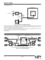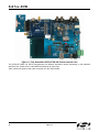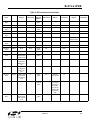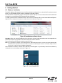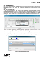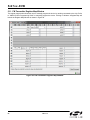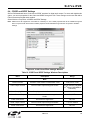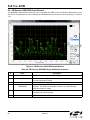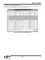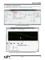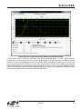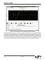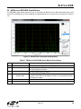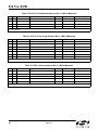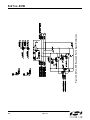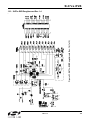
1
Si 4 7 x x - EVB Si47 XX E VALUATION B OA RD U SER ’ S G UIDE 1. Introduction Thank you for purchasing the Silicon Laboratories, Inc. Si47xx Evaluation Board (EVB). The EVB and associated software have been designed to speed up the overall development process. We look forward to working with you, and have posted support articles, answers to frequently asked questions, and application notes at www.mysilabs.com. Table 1 describes all of the available products and features in the Si47xx family. Si4700 FM Receiver Si4701 FM Receiver with RDS Si4702 FM Receiver Si4703 FM Receiver with RDS Si4704 FM Receiver Si4705 FM Receiver with RDS 2 Si47061 High Performance RDS Receiver Si47071 WB Receiver with SAME Si4708 FM Receiver Si4709 FM Receiver with RDS Si4710 FM Transmitter Si4711 FM Transmitter with RDS Si4712 FM Transmitter with RPS Si4713 FM Transmitter with RDS & RPS Si4720 FM Transceiver Si4721 FM Transceiver with RDS Si4730 AM/FM Receiver Si4731 AM/FM Receiver with RDS Package Size (mm) AEC-Q100 Qualified Embedded FM antenna Digital Output Digital Input SAME RPS High Performance RDS RDS WB Receiver SW/LW Receiver AM Receiver General Description FM Receiver Part Number FM Transmitter Table 1. Product Family Function 4x4 4x4 3x3 3x3 3x3 3x3 3x3 3x3 2.5x2.5 2.5x2.5 3x3 3x3 3x3 3x3 3x3 3x3 3x3 2 3x3 Notes: 1. Si4706, Si4707, and Si474x are covered under NDA. 2. High Performance RDS is available in Si4705/31/35/85-D50 and later. Rev. 0.8 2/12 Copyright © 2012 by Silicon Laboratories Si47xx-EVB Si47xx-EVB Si4736 AM/FM/WB Receiver Si4737 AM/FM/WB Receiver with RDS Si4738 FM/WB Receiver Si4739 FM/WB Receiver with RDS Si47401 AM/FM Receiver AM/FM Receiver with RDS Si47421 AM/LW/SW/FM/WB Receiver Si47431 AM/LW/SW/FM/WB Receiver with RDS Si47441 AM/LW/SW/FM Receiver Si47451 AM/LW/SW/FM Receiver with RDS Si47491 High-Performance RDS Receiver Si4784 FM Receiver Si4785 FM Receiver with RDS Si4741 1 3x3 2 3x3 3x3 2 3x3 Rev. 0.8 3x3 3x3 Notes: 1. Si4706, Si4707, and Si474x are covered under NDA. 2. High Performance RDS is available in Si4705/31/35/85-D50 and later. 2 Package Size (mm) AEC-Q100 Qualified AM/SW/LW/FM Receiver with RDS Embedded FM antenna Si4735 Digital Output Digital Input SAME RPS AM/SW/LW/FM Receiver General Description High Performance RDS Si4734 Part Number RDS WB Receiver AM Receiver SW/LW Receiver FM Receiver FM Transmitter Table 1. Product Family Function (Continued) 4x4 4x4 4x4 4x4 4x4 4x4 4x4 3x3 3x3 Si47xx-EVB TABLE O F C ONTENTS 1. Introduction . . . . . . . . . . . . . . . . . . . . . . . . . . . . . . . . . . . . . . . . . . . . . . . . . . . . . . . . . . . . .1 2. Description . . . . . . . . . . . . . . . . . . . . . . . . . . . . . . . . . . . . . . . . . . . . . . . . . . . . . . . . . . . . . .8 2.1. Si47xx Baseboard . . . . . . . . . . . . . . . . . . . . . . . . . . . . . . . . . . . . . . . . . . . . . . . . . . . .8 2.2. Si47xx Daughtercards . . . . . . . . . . . . . . . . . . . . . . . . . . . . . . . . . . . . . . . . . . . . . . . . 15 3. Recommended Hardware Setup . . . . . . . . . . . . . . . . . . . . . . . . . . . . . . . . . . . . . . . . . . . . 28 3.1. Hardware Setup for FM Transmitter Test . . . . . . . . . . . . . . . . . . . . . . . . . . . . . . . . . 28 3.2. Hardware Setup for FM or Weather Band Receiver Test . . . . . . . . . . . . . . . . . . . . .29 3.3. Hardware Setup for AM Receiver Test . . . . . . . . . . . . . . . . . . . . . . . . . . . . . . . . . . .30 4. Getting Started . . . . . . . . . . . . . . . . . . . . . . . . . . . . . . . . . . . . . . . . . . . . . . . . . . . . . . . . . . 32 4.1. Software Installation . . . . . . . . . . . . . . . . . . . . . . . . . . . . . . . . . . . . . . . . . . . . . . . . . 32 4.2. Board Initialization . . . . . . . . . . . . . . . . . . . . . . . . . . . . . . . . . . . . . . . . . . . . . . . . . . .33 4.3. Switching Functions . . . . . . . . . . . . . . . . . . . . . . . . . . . . . . . . . . . . . . . . . . . . . . . . . 36 4.4. State Management . . . . . . . . . . . . . . . . . . . . . . . . . . . . . . . . . . . . . . . . . . . . . . . . . . 37 4.5. Disconnecting the EVB . . . . . . . . . . . . . . . . . . . . . . . . . . . . . . . . . . . . . . . . . . . . . . . 39 5. FM Transmitter GUI . . . . . . . . . . . . . . . . . . . . . . . . . . . . . . . . . . . . . . . . . . . . . . . . . . . . . . 40 5.1. Configuring the Si47xx as an FM Transmitter Using Analog Audio Input . . . . . . . . . 40 5.2. Configuring the Si47xx as an FM Transmitter Using Digital Audio with Analog Audio Source . . . . . . . . . . . . . . . . . . . . . . . . . . . . . . . . . . . . . . . . . . . . . . . . .41 5.3. Configuring the Si47xx as an FM Transmitter Using Digital Audio with SPDIF Digital Source . . . . . . . . . . . . . . . . . . . . . . . . . . . . . . . . . . . . . . . . . . . . . . . . 42 5.4. FM Transmitter Main Window . . . . . . . . . . . . . . . . . . . . . . . . . . . . . . . . . . . . . . . . . .43 5.5. FM Transmitter Settings (Analog Mode) Property Window . . . . . . . . . . . . . . . . . . . . 45 5.6. FM Transmitter Settings (Digital Mode) Property Window . . . . . . . . . . . . . . . . . . . . 47 5.7. CODEC Settings . . . . . . . . . . . . . . . . . . . . . . . . . . . . . . . . . . . . . . . . . . . . . . . . . . . . 49 5.8. SPDIF Settings . . . . . . . . . . . . . . . . . . . . . . . . . . . . . . . . . . . . . . . . . . . . . . . . . . . . . 50 5.9. FM Transmitter Receive Power Scan Window . . . . . . . . . . . . . . . . . . . . . . . . . . . . . 51 5.10. FM Transmitter Radio Data Service (RDS) . . . . . . . . . . . . . . . . . . . . . . . . . . . . . . . 52 5.11. FM Transmitter Register Map Window . . . . . . . . . . . . . . . . . . . . . . . . . . . . . . . . . . 60 6. FM Receiver GUI . . . . . . . . . . . . . . . . . . . . . . . . . . . . . . . . . . . . . . . . . . . . . . . . . . . . . . . . . 61 6.1. Configuring the Si47xx as an FM Receiver . . . . . . . . . . . . . . . . . . . . . . . . . . . . . . . . 61 6.2. FM Receiver Main Window . . . . . . . . . . . . . . . . . . . . . . . . . . . . . . . . . . . . . . . . . . . . 62 6.3. FM Receiver Settings Property Window . . . . . . . . . . . . . . . . . . . . . . . . . . . . . . . . . . 64 6.4. CODEC and SPDIF Settings . . . . . . . . . . . . . . . . . . . . . . . . . . . . . . . . . . . . . . . . . . . 73 6.5. FM Receiver RDS Window . . . . . . . . . . . . . . . . . . . . . . . . . . . . . . . . . . . . . . . . . . . . 74 6.6. FM Receiver RDS Settings . . . . . . . . . . . . . . . . . . . . . . . . . . . . . . . . . . . . . . . . . . . . 77 6.7. FM UI Settings . . . . . . . . . . . . . . . . . . . . . . . . . . . . . . . . . . . . . . . . . . . . . . . . . . . . . 79 6.8. FM Receiver RSSI/SNR Graph Window . . . . . . . . . . . . . . . . . . . . . . . . . . . . . . . . . . 80 6.9. FM Receiver Register Map Window . . . . . . . . . . . . . . . . . . . . . . . . . . . . . . . . . . . . . 81 6.10. FM Receiver Logging Tools . . . . . . . . . . . . . . . . . . . . . . . . . . . . . . . . . . . . . . . . . . 82 6.11. FM Receiver Configuration Helper . . . . . . . . . . . . . . . . . . . . . . . . . . . . . . . . . . . . . 83 7. Weather Band GUI . . . . . . . . . . . . . . . . . . . . . . . . . . . . . . . . . . . . . . . . . . . . . . . . . . . . . . . 90 7.1. WB Receiver Initialization . . . . . . . . . . . . . . . . . . . . . . . . . . . . . . . . . . . . . . . . . . . . . 90 7.2. Weather Band Main Window . . . . . . . . . . . . . . . . . . . . . . . . . . . . . . . . . . . . . . . . . . . 91 Rev. 0.8 3 Si47xx-EVB 7.3. Weather Band Settings Property Window . . . . . . . . . . . . . . . . . . . . . . . . . . . . . . . . . 92 7.4. Weather Band Receiver RSSI/SNR Graph Window . . . . . . . . . . . . . . . . . . . . . . . . . 94 7.5. Weather Band Receiver Register Map Window . . . . . . . . . . . . . . . . . . . . . . . . . . . . 95 7.6. Weather Band Receiver SAME Event Data (Si4707 only) . . . . . . . . . . . . . . . . . . . . 96 8. AM Receiver GUI . . . . . . . . . . . . . . . . . . . . . . . . . . . . . . . . . . . . . . . . . . . . . . . . . . . . . . . . 97 8.1. AM Receiver Initialization . . . . . . . . . . . . . . . . . . . . . . . . . . . . . . . . . . . . . . . . . . . . .97 8.2. AM Receiver Main Window . . . . . . . . . . . . . . . . . . . . . . . . . . . . . . . . . . . . . . . . . . . . 98 8.3. AM Receiver Property Settings Window . . . . . . . . . . . . . . . . . . . . . . . . . . . . . . . . . 100 8.4. AM Receiver RSSI/SNR Graph Window . . . . . . . . . . . . . . . . . . . . . . . . . . . . . . . . . 105 8.5. AM Receiver Register Map Window . . . . . . . . . . . . . . . . . . . . . . . . . . . . . . . . . . . . 106 8.6. AM Receiver Logging Tools Info . . . . . . . . . . . . . . . . . . . . . . . . . . . . . . . . . . . . . . . 107 8.7. AM Receiver Configuration Helper . . . . . . . . . . . . . . . . . . . . . . . . . . . . . . . . . . . . .108 9. Using the EVB with a 9 V Battery . . . . . . . . . . . . . . . . . . . . . . . . . . . . . . . . . . . . . . . . . . 109 10. Debugging Guidelines for Si47xx EVB . . . . . . . . . . . . . . . . . . . . . . . . . . . . . . . . . . . . . 110 11. Bill of Materials . . . . . . . . . . . . . . . . . . . . . . . . . . . . . . . . . . . . . . . . . . . . . . . . . . . . . . . . 112 12. Schematics . . . . . . . . . . . . . . . . . . . . . . . . . . . . . . . . . . . . . . . . . . . . . . . . . . . . . . . . . . . 124 12.1. Si47xx-EVB Baseboard Rev 1.6 . . . . . . . . . . . . . . . . . . . . . . . . . . . . . . . . . . . . . . 124 12.2. Si471x/2x-EVB Daughtercard Rev 1.4 . . . . . . . . . . . . . . . . . . . . . . . . . . . . . . . . . 131 12.3. Si473x-EVB Daughtercard Rev. 1.4 . . . . . . . . . . . . . . . . . . . . . . . . . . . . . . . . . . . 133 12.4. Si474x–EVB Daughtercard Rev 1.3 . . . . . . . . . . . . . . . . . . . . . . . . . . . . . . . . . . . 135 12.5. Si4749-EVB Daughtercard Rev 1.1 . . . . . . . . . . . . . . . . . . . . . . . . . . . . . . . . . . . 137 12.6. Antenna Card Schematics . . . . . . . . . . . . . . . . . . . . . . . . . . . . . . . . . . . . . . . . . . 139 13. Layout . . . . . . . . . . . . . . . . . . . . . . . . . . . . . . . . . . . . . . . . . . . . . . . . . . . . . . . . . . . . . . . 141 13.1. Si47xx-EVB Baseboard Rev 1.6 . . . . . . . . . . . . . . . . . . . . . . . . . . . . . . . . . . . . . . 141 13.2. Si471x/2x-EVB Daughtercard Rev 1.4 . . . . . . . . . . . . . . . . . . . . . . . . . . . . . . . . . 144 13.3. Si473x-EVB Daughtercard Rev 1.4 . . . . . . . . . . . . . . . . . . . . . . . . . . . . . . . . . . . . 147 13.4. Si474x-EVB Daughtercard Rev 1.3 . . . . . . . . . . . . . . . . . . . . . . . . . . . . . . . . . . . . 150 13.5. Si4749-EVB Daughtercard Rev 1.1 . . . . . . . . . . . . . . . . . . . . . . . . . . . . . . . . . . . 152 13.6. Antenna Cards . . . . . . . . . . . . . . . . . . . . . . . . . . . . . . . . . . . . . . . . . . . . . . . . . . .155 Documentation Change List . . . . . . . . . . . . . . . . . . . . . . . . . . . . . . . . . . . . . . . . . . . . . . . . 163 Contact Information . . . . . . . . . . . . . . . . . . . . . . . . . . . . . . . . . . . . . . . . . . . . . . . . . . . . . . .164 4 Rev. 0.8 Si47xx-EVB This user's guide contains information related to only the Si47xx EVBs itemized in Table 2. Table 2 serves as a quick reference guide for the sections of interest for your EVB. Sections 1, 4, 9, and 10 of the document apply to all EVBs. Table 2. Quick Reference Guide Part Description Recommended HW Setup GUI Bill of Materials Schematics Layout Si4704/05/ 06/84/85 Sections 2.1., 2.2.1., and 2.2.6. Section 3.2. Section 6. Section 11. Tables Sections 12.1., Sections 29 and 30 12.2. 13.1., 13.2. Si4707 Section 2.2.2., 2.2.5., 2.2.6. Section 3.2. Section 7. Section 11., Tables 29 and 31 Si4710/11/ 12/13 Sections 2.1., 2.2.1., 2.2.6. Section 3.1. Section 5. Section 11. Tables Sections 12.1., Sections 29 and 30 12.2. 13.1., 13.2. Si4720/21 Sections 2.1., 2.2.1., 2.2.6. Sections 3.1. and 3.2. Sections 5. and 6. Section 11. Tables Sections 12.1., Sections 29 and 30 12.2. 13.1., 13.2. Si4730/31 Sections 2.1., 2.2.2., 2.2.5., 2.2.6 Sections 3.2. and 3.3. Sections 6. and 8. Section 11. Tables Sections 12.1., Sections 29, 31, 34, 35, and 12.3., 12.6.1., 13.1., 13.3., 36 12.6.2. 13.6.1., 13.6.2. Si4734/35 Sections 2.1., 2.2.2., 2.2.5., 2.2.6. Sections 3.2. and 3.3. Sections 6. and 8. Section 11. Tables Sections 12.1., Sections 29 and 37 12.3., 12.6.3. 13.1., 13.3., 13.6.3. Si4736/37 Sections 2.1., 2.2.2., 2.2.5., 2.2.6. Sections 3.2. and 3.3. Sections 6., 7., and 8. Section 11. Tables Sections 12.1., Sections 29 and 37 12.3., 12.6.3. 13.1., 13.3., 13.6.3. Si4738/39 Sections 2.1., 2.2.2., 2.2.5., 2.2.6. Sections 3.2. and 3.3. Sections 6., and 7. Section 11. Tables Sections 12.1., Sections 29 and 37 12.3., 12.6.3. 13.1., 13.3., 13.6.3., Si4740/41/ Section 2.1., 42/43/44/45 2.2.3., 2.2.5., 2.2.6. Sections 3.2. and 3.3. Sections 7. and 8. Section 11., Table Sections 12.1., Sections 29, 32, 37 12.4., 12.6.4. 13.1., 13.4.,13.6.4. Section 3.2. Section 6. Section 11. Tables Sections 12.1., Section 29 and 33 12.5. 13.1., 13.5. Si4749 Sections 2.1., 2.2.4. , 2.2.6. Rev. 0.8 Section 12.1., 12.3. Section 13.1., 13.3. 5 Si47xx-EVB There are ten different EVB kits within the Si47xx family. Each kit ships with a standard set of components that are common to all kits and a unique set that depends on the EVB kit P/N. Standard set of components are: Customer welcome and evaluation letter Characterization Report USB cable RCA cable 9 V battery Headphones Si47xx CD including: EVB Data sheet Development application GUI rev 2.5.4 or later guide Quick start guide. The unique set of components for each EVB kit is defined in Table 3. User's Table 3. Si47xx-EVB Kit Unique Contents Adapters EVB Kit Base Board Daughtercard Antenna Cards Antennas BNC Male to RCA Female SMA Male to BNC Female SMA Female to BNC Male SMA Male to SMA Male Si4705-EVB Si471x/2x Si47xx Base board Daughtercard Rev1.3 or Rev1.2 or later later — — Yes No No No Si4706-EVB Si471x/2x Si47xx Base board Daughtercard Rev1.3 or Rev1.2 or later later — — Yes No No No Si4707-EVB Si473x Si47xx Base board Daughtercard Rev1.3 or Rev1.2 or later later SAME antenna Whip antenna Yes No No No Si4713-EVB Si471x/2x Si47xx Base board Daughtercard Rev1.3 or Rev1.2 or later later — — Yes No No No Si4721-EVB Si471x/2x Si47xx Base board Daughtercard Rev1.3 or Rev1.2 or later later — — Yes No No No Si4731-EVB Si473x 4731 antenna Si47xx Base board Daughtercard kit (large ferRev1.3 or Rev1.2 or later rite, medium ferrite, air loop later transformer) Loop antenna Yes No No No 6 Rev. 0.8 Si47xx-EVB Table 3. Si47xx-EVB Kit Unique Contents (Continued) Adapters EVB Kit Base Board Daughtercard Antenna Cards Antennas BNC Male to RCA Female SMA Male to BNC Female SMA Female to BNC Male SMA Male to SMA Male Si4735-EVB Si47xx Base board Rev1.3 or later Si473x Daughter Card Rev1.2 or later SW antenna Whip antenna Yes No No No Si4737-EVB Si47xx Base board Rev1.3 or later Si473x Daughter Card Rev1.2 or later WB antenna Whip antenna Yes No No No Si4743-EVB Si47xx Base board Rev1.3 or later Si474x Daughter Card Rev1.3 or later Antenna Dummy Whip antenna Yes Yes No Yes Si4749-EVB Si47xx Base board Rev1.3 or later Si4749 Daughter Card Rev1.0 or later — Whip antenna Yes No Yes No Rev. 0.8 7 Si47xx-EVB 2. Description Si47xx EVB consists of a baseboard, a daughtercard with the Si47xx part pre-mounted, and, if applicable, an antenna card. The baseboard is common and shared among all Si47xx EVBs. The following sections refer to both the images in the figures and the silkscreen on the Si47xx EVB. Please refer to both when using this guide. 2.1. Si47xx Baseboard J6 J27 J30 J52 J57 X1 J61 J54 J68 J69 J75 J76 U22 D1 J79 J74 PB1 SW1 J78 Figure 1. Baseboard Connectors, Jumpers, and Devices Baseboard power connectors/devices: J79 J78 J77 USB connector (using USB power) External power connector Battery connector J76 SW1 J61 J68 J69 Terminal block (TB) power connector Switch to select between USB power or Ext power Jumper: Baseboard power select (3.3 V or TB) Jumper: Si47xx VIO power select (3.3 V or adjustable voltage via R73 or TB) Jumper: Si47xx VDD power select (3.3 V or adjustable voltage via R74 or TB) 8 Rev. 0.8 J77 Si47xx-EVB Baseboard audio I/O connectors: J6 J30 RCA output Line output Note: Line output will not be supported on new EVBs as of February 14, 2011. Baseboard clock connectors/devices: X1 32.768 kHz crystal oscillator J52 Solder bump: select internal RCLK from oscillator J54 Ext RCLK SMA connector input J57 Jumper: Enable or Disable Int RCLK Baseboard MCU connectors/devices: U22 C8051F342 MCU J79 USB connector to communicate with the MCU J74 JTAG connector for the MCU PB1 Push button to reset the MCU D1 LED to confirm power supply to the MCU Baseboard to Daughtercard connectors: J27 Si47xx daughtercard connector J75 Expansion card connector (reserved) 2.1.1. Power Supply Network Daughterboard J78 EXT LDO 1.25–7 V (R74) ADJ Jumper J69 +3.3 V VIO TB LDO 1.25–3.9 V (R73) 11 VDD 10 TB +3.3 V SW1 ADJ Jumper J68 Si47xx TB Jumper J61 LDO +3.3 V (U17) J79 USB +3.3 V Vmcu VIO VDD Vm Vio Vdd Gnd J77 BATT J76 Terminal Block (TB) Figure 2. Power Supply Block Diagram Rev. 0.8 9 Si47xx-EVB The Si47xx EVB can be powered using one of the following power supply options: 1. USB power supply via J79 2. External dc (Ext DC) power supply via power jack J78 or battery via J77 3. Three separate power supplies (Vdd, Vio, Vmcu) via terminal block J76 The EVB has three supply rails: Vdd, Vio, and Vmcu. Vdd and Vio are routed directly to the daughtercard to power the Vdd and Vio pins on the Si47xx chip, while Vmcu is used to power the baseboard. The external dc power supply and battery should not be connected simultaneously. Refer to Section 9. "Using the EVB with a 9 V Battery‚" on page 109 for more information. USB Power Supply & EXT DC Power Supply Switch SW1 is used to select between the USB power supply and Ext dc power supply. The USB power supply or the Ext dc power supply can be configured in one of the following two modes: 1. Fixed +3.3 V 2. Adjustable Vdd and Vio Fixed +3.3 V ADJ +3.3V TB J68 J69 Vmcu +3.3V Vdd TB Vio ADJ +3.3V TB Only one LDO is used in this mode which outputs a +3.3 V supply to all three rails (Vdd, Vio, and Vmcu). The jumpers need to be set according to Figure 3 to use the EVB in this configuration. This is the default configuration on the EVB. J61 Figure 3. Default Fixed +3.3 V Jumpers Setting Terminal Block Power Supply ADJ +3.3V TB J68 J69 Vmcu +3.3V Vdd TB Vio ADJ +3.3V TB If the terminal block supplies are used, then jumpers J61, J68, and J69 need to be set according to Figure 4. The user then needs to connect three different power supplies for Vdd, Vio, and Vmcu. J61 Figure 4. Terminal Block Jumpers Setting 10 Rev. 0.8 Si47xx-EVB 2.1.2. Microcontroller TC_BCLK (reserved for digital Rx ) Jumper J41 Daughterboard S_GPO3/DCLK MD_GPIO3 MS_GPIO2 MD_GPIO1 J79 USB J74 JTAG GPO1 GPO2 GPO3/ DCLK Jumper J65 MCU C8051F342 PB1 Reset SD_GPO1 MD_GP4 19 18 17 MS_RSTB RST~ 5 Si47xx SEN~ SCLK SDIO 6 7 8 MS_SENB MS_SCLK MS_SDIO Figure 5. MCU Block Diagram The Si47xx EVB uses a Silicon Laboratories' C8051F342 microcontroller to control the Si47xx and to provide USB connectivity from the host PC (via connector J79). The LED D1 illuminates to confirm that power is being properly supplied to the C8051F342 and firmware has loaded. Push-button PB1 manually resets the C8051F342. The JTAG connector J74 is used to program the C8051F342 at production time, and is not required thereafter. Rev. 0.8 11 Si47xx-EVB 2.1.3. Reference Clock Daughterboard Jumper J57 X1 32.768 kHz INT RClk DIS_INT_RCLK Si47xx INT_RCLK 9 RCLK Jumper J52 EXT_RCLK J54 EXT RClk Figure 6. Reference Clock Block Diagram The Si47xx accepts a 32.768 kHz reference clock at the RCLK pin. On the EVB, this clock is provided by a precision crystal oscillator. The user has the option of not using the onboard oscillator and bringing in the reference clock from an external source through SMA connector J54. When the user chooses to provide an external RCLK, jumper J52 has to be set accordingly. The user has the option to turn off the onboard crystal oscillator by installing jumper J57. 2.1.4. Audio I/O EVB In (TX only) 47xx Audio2 47xx Audio1 EVB Out (RX only) TX: Analog/Digital In TX: Analog In RX: Digital Out TX: Digital In RX: Analog Out RX: Analog/Digital Out Audio2 Select J7 RCA In Jumper J5&J13 Audio1 Select AUDIO2 1 J19 Line In (white) 0 CODEC IN LINE IN AUDIO2 AUDIO1 16 LIN/ DFS2 LOUT/ DFS1 14 15 RIN/ DOUT ROUT/ DIN 13 Si47xx (Daughterboard) 0 0 1 1 J30 Line Out (black) CODEC OUT AUDIO1 LINE OUT DIN DOUT 0 J6 RCA Out To_TX From_RX 1 J19 SPDIF In (white) S/PDIF IN Jumper J45 From_RX To_TX Jumper J44 SPDIF DOUT IN S/PDIF OUT DIN SPDIF OUT Digital Input Select Note: Jumper J44 and J45 are automatically configured in EVB Rev 1.3. Figure 7. Audio I/O Block Diagram 12 Rev. 0.8 J30 SPDIF Out (black) Si47xx-EVB The EVB supports three different kinds of configurations for the FM transmitter: Analog In to Analog In In to Digital In Digital In to Digital In Analog Analog In to Analog In: This configuration provides a way for the user to evaluate the analog audio input for FM transmission. The input to the EVB is an analog audio provided via the RCA input connector J7 or LINE In connector J19 (white). Jumpers J5 and J13 are set to RCA input by default. The user has to change this jumper accordingly if LINE In is being used. Then the analog audio input is routed directly through a switch to the Si47xx Rin/Lin inputs pin 15 and 16 (Audio2). Analog In to Digital In: This configuration provides a way for the user to evaluate the Si47xx digital audio input for FM transmission using an analog audio input. The input to the EVB is an analog audio provided via the RCA input connector J7 or LINE In connector J19 (white). Jumpers J5 and J13 are set to RCA input by default. The user has to change this jumper accordingly if LINE In is being used. Then the analog audio input is converted by CODEC U10 to a serial audio digital data before it is routed to the Si47xx digital audio input DIO and DFS pin 13 and 14 (Audio1). The DCLK input is routed to the GPO3/DCLK pin 17. Make sure that jumper J41 is set to DCLK to ensure proper operation. Digital In to Digital In: This configuration provides a way for the user to evaluate the Si47xx digital audio input for FM transmission using S/PDIF digital audio commonly found in sound cards. The input to the EVB is a digital S/PDIF data provided via the S/PDIF In connector J19 (white). The digital S/PDIF input is converted by S/PDIF Translator U9 to a serial audio digital data before it is routed to the Si47xx digital audio input DIO and DFS pin 13 and 14 (Audio1). The DCLK input is routed to the GPO3/DCLK pin 17. Make sure that jumper J41 is set to DCLK to ensure proper operation. Note: Digital in through J19 will not be supported on new EVBs as of February 14, 2011. The EVB supports three different kinds of configurations for the FM receiver: Analog Out to Analog Out Digital Out to Digital and Analog Out Dual Output (Digital and Analog Out) Analog Out to Analog Out: This configuration provides a way for the user to evaluate the analog audio output for receiver operation. The output of the Si47xx is routed to RCA output connector J6 and Line output connector J30. Digital Out to Digital and Analog Out: This configuration provides a way for the user to evaluate the digital audio output for FM and AM receive using either S/PDIF digital audio or analog audio through the onboard CODEC. The Si47xx digital audio out is routed through the S/PDIF translator µ9 to S/PDIF output connector J30 and routed through the CODEC to RCA output connector J6 and line output connector J30. Note: Digital output through J30 will not be supported on new EVBs as of February 14, 2011. Dual Output (Digital and Analog Out): This configuration provides a way for the user to evaluate the analog audio out and digital audio using S/PDIF digital audio for FM and AM. The analog output of the Si47xx is routed to RCA output connector J6 and line output connector J30 and the digital audio out is routed through the S/PDIF translator to S/PDIF output connector J30. Note: Digital output through J30 will not be supported on new EVBs as of February 14, 2011. Rev. 0.8 13 Si47xx-EVB IMPORTANT: Jumper Settings Because of the many possibilities available to configure the EVB, ensure that these four jumpers are set accordingly: 1. J41: GPO3/DCLK setting 2. J44: TX/RX setting for Audio1 I/O (automatically set by the GUI for baseboard 1.3 and later) 3. J45: TX/RX setting for Audio2 I/O (automatically set by the GUI for baseboard 1.3 and later) 4. J5, J13: Analog Audio Source, RCA or Line In J41: GPO3/DCLK Setting Upper—DCLK digital audio clock Lower—GPO3 digital control signal For configuring the Si47xx digital audio input, make sure that the jumper is set in the Upper position so that the DCLK signal will be routed to the Si47xx. J44: TX/RX Setting for Audio1 I/O (automatically set by the GUI for baseboard 1.3 and later) Upper—Audio1 is set to FM transmit (pin 13 and 14 will be the digital audio input). Lower—Audio1 is set for FM receive (pin 13 and 14 will be analog/digital audio output). J45: TX/RX Setting for Audio2 I/O (automatically set by the GUI for baseboard 1.3 and later) Upper—Audio2 is set to FM transmit (pin 15 and 16 will be the analog/digital audio input). Lower—Audio2 is set for FM receive (pin 15 and 16 will be the digital audio output). J5, J13: Analog Audio Source, RCA or Line In Upper—RCA inputs are used for analog audio source. Lower—Line inputs are used for analog audio source. 14 Rev. 0.8 Si47xx-EVB 2.2. Si47xx Daughtercards 2.2.1. Si471x/2x Daughtercard Figure 8. Si471x/2x Daughtercard Connectors and Devices Daughtercard Connectors and Components: U1 Si472x FM Transceiver or Si470x FM Receiver or Si471x FM Transmitter L2 Tuning Inductor R2 0 resistor to connect FM TX output to 10 cm trace built-in antenna C8 2 pF capacitor to connect FM TX output to J1 SMA connector R4 50 termination resistor J1 J2 J28 SMA connector for FM transmitter output or FM receiver input for embedded antenna Header for putting external antenna for FM transmitter or embedded antenna for FM receiver SMA connector for FM receiver input J29 Headphone jack for FM receiver Rev. 0.8 15 Si47xx-EVB Figure 9. Fully Assembled Si471x/2x EVB Si470x/1x/2x EVBs use Si471x/2x daughtercard with different population options depending on the individual Si470x/1x/2x part. Please refer to individual Bill of Materials for each board. 16 Rev. 0.8 Si47xx-EVB 2.2.2. Si473x Daughtercard Figure 10. Si473x Daughtercard Connectors and Devices Daughtercard connectors and components: J1 SMA connector for AM test circuit (does not apply to Si4707-EVB) J2 J24 J26 L4 U1 C2 C3 C8 C12 C13 Header for antenna interface connection Headphone jack SMA connector for FM test circuit 270 nH inductor for FM input Si473x AM/FM/SW Weather Band Receiver chip (or Si4707 WB/Same receiver for Si4707-EVB only) Vdd bypass capacitor FM test circuit ac coupling capacitor AM input ac coupling capacitor FM input ac coupling capacitor AM test circuit ac coupling capacitor Rev. 0.8 17 Si47xx-EVB Figure 11. Fully Assembled Si473x-EVB with Ferrite Antenna Card The Si473x/07 EVBs use Si473x daughtercard with different population options depending on the individual Si473x/07 part. Please refer to individual Bill of Materials for each card. Table 4 shows the antenna and audio connections for the Si47xx EVBs. 18 Rev. 0.8 Si47xx-EVB 2.2.3. Si474x Daughtercard Figure 12. Si474x Daughtercard Connectors and Devices Daughtercard connectors and components: J4 BNC connector for antenna connection C6, C1, C18 Vdd bypass capacitor C2 FM matching component L1, L5 FM matching component Q1–2 Cascode amplifier for AM front-end boost circuit. U1 Si4740/41/42/43 AM/FM Receiver chip The daughtercard implements the Si4740/41/42/43 AM/FM RDS receive solution. The Si474x daughtercard also has a cascode amplifier circuit made up of two transistors to provide gain boost for AM front-end. The on-chip De-Q resistors will then be used to adjust the overall circuit gain. In cases where the AM reception is too strong, the front-end attenuators can be engaged by using GPIO1 as the control signal. Rev. 0.8 19 Si47xx-EVB Figure 13. Fully Assembled Si474x-EVB 20 Rev. 0.8 Si47xx-EVB 2.2.4. Si4749 Daughtercard Figure 14. Si4749 Daughtercard Connectors and Devices Daughtercard connectors and components: J1 SMA connector for pass-thru FM connection J2 SMA connector for FM antenna connection C2 Vdd bypass capacitor L1 FM matching component U2 Si4749 RDS Receiver The daughtercard implements the Si4749 RDS receive solution. The SMA connector, J2, allows the user to attach a whip antenna for FM reception or a signal generator for FM test circuit. A pass-thru connection, J1, is also present to provide the FM signal to other FM receivers if necessary. Rev. 0.8 21 Si47xx-EVB Figure 15. Fully Assembled Si4749-EVB 22 Rev. 0.8 Si47xx-EVB 2.2.5. Antenna Interfaces 2.2.5.1. AM Antenna Interface Figure 16. Antenna Board Options—SL4X30MW100T (Medium Ferrite), SL5X7X100MW70T (Large Ferrite), and SL9X5X4MWTF Airloop The user has the flexibility of choosing one of the two available antenna options. The user can either decide to use the airloop antenna or the ferrite loop stick antenna. Rev. 0.8 23 Si47xx-EVB 2.2.5.2. SW and Weather Band Antenna Interfaces Figure 17. SW/WB Antenna Card (SW Population) and (WB Population) The BNC connector, J2, will be used to connect a whip antenna for shortwave, FM, and weather band reception. For SW reception, switch S1 must be in the SW position. The ferrite bar is used for AM reception, and the switch S1 must be in the AM position for AM reception. When using the WB Antenna Card, WB reception is through the whip antenna. For a better listening experience, plug the headphones to J30 rather than J24. Note: LW not supported with SW/WB Antenna Card. 2.2.5.3. Si474x Antenna Dummy Card Figure 18. Si474x Antenna Dummy Card 24 Rev. 0.8 Si47xx-EVB Table 4. Si47xx Antenna Connections EVB Kit Name Receiver AM Antenna Options AM Connections FM Antenna Options FM Connections Si4705-XEVB Si4705 None None Headphone J29 Trace J2 Headphone J29 Trace J2 Si4706-XEVB Si4707-BEVB Si4706 Si4707 None None None None SW Antenna Options None SW Connections WB Antenna Options None None None None None Headphone J24 Whip/SAME Antenna Card J2 Headphone J24 Si4713-BEVB Si4713 None None Trace J2 None Si4721-BEVB Si4721 None None Headphone J29 None Trace J2 Headphone J24 Headphone J24 Whip/SW Antenna Card Whip/SW Antenna Card J2 For SW reception, set the S1 switch to SW position. LW is not supported by the SW antenna card. Headphone J24 Si4731-XEVB Si4735-XEVB Si4737-XEVB Si4731 Si4735 Si4737 SL5X7X100M W70T Ferrite / Large Ferrite J2 SL4X30MW1 10T Ferrite / Medium Ferrite J2 SL9X5X4MW TF Autotransformer / Air loop J2 SL5X7X100M W70T Ferrite / SW Antenna card J2 SL5X7X100M W70T Ferrite / WB Antenna card J2 Rev. 0.8 WB Connections None J2 None 25 Si47xx-EVB Table 4. Si47xx Antenna Connections (Continued) EVB Kit Name Receiver AM Antenna Options FM Antenna Options FM Connections Whip/WB Antenna Card J2 AM Connections SW Antenna Options SW Connections Si4743-CEVB Si4743 Whip / Si474x Antenna Dummy card J4 Whip J4 Whip Si4749-CEVB Si4749 None None Whip J2 None WB Antenna Options WB Connections Whip/WB Antenna Card. For WB reception, set the S1 switch to WB position J2 Table 5. Si47xx Audio Connections EVB Kit Name Receiver Audio Out Options Audio Out Connections Audio In Options Audio Connections Si4705-X-EVB Si4705 Headphone J29 None None Unity Gain Buffer / RCA J6 (Baseboard) Headphone J29 None None Unity Gain Buffer / RCA J6 (Baseboard) None None Si4706-X-EVB Si4707-B-EVB Si4706 Si4707 Headphone J29 Unity Gain Buffer / RCA J6 (Baseboard) Si4713-B-EVB Si4713 None None Unity Gain Buffer / RCA J7 (Baseboard) Si4721-B-EVB Si4721 Headphone J29 Unity Gain Buffer / RCA J7 (Baseboard) Unity Gain Buffer / RCA J6 (Baseboard) Headphone J24 None None Unity Gain Buffer / RCA J6 (Baseboard) Headphone J24 None None Unity Gain Buffer / RCA J6 (Baseboard) Headphone J24 None None Unity Gain Buffer / RCA J6 (Baseboard) Si4731-X-EVB Si4735-X-EVB Si4737-X-EVB Si4731 Si4735 Si4737 Si4743-C-EVB Si4743 Unity Gain Buffer / RCA J6 (Baseboard) None None Si4749-C-EVB Si4749 None None None None 26 Rev. 0.8 Si47xx-EVB 2.2.6. Test Circuit Interfaces Table 6 shows the test circuit interface connections for Si47xx EVBs. Table 6. Si47xx Test Circuit Connections EVB Kit Name Receiver AM/SW/LW Test Options AM/SW/LW Connections FM Test Options FM Connections Audio Out Test Options Audio Out Connections Audio In Test Options Audio In Connections Si4705-X-EVB Si4705 None None FMI / SMA J28 through C1. Remove C9 for best sensitivity Unity Gain Buffer / RCA J6 (Baseboard) None None LPI / SMA J1 J28 through C1. Remove C9 for best sensitivity Unity Gain Buffer / RCA J6 (Baseboard) None None Si4706-X-EVB Si4706 None None FMI / SMA LPI / SMA J1 Si4707-B-EVB Si4707 None None FMI / SMA J26 Unity Gain Buffer / RCA J6 (Baseboard) None None Si4713-B-EVB* Si4713 None None LPI / SMA J1 None None Unity Gain Buffer / RCA J7 Si4721-B-EVB Si4721 None None FMI / SMA J28 through C1. Remove C9 for best sensitivity Unity Gain Buffer / RCA J6 (Baseboard) Unity Gain Buffer / RCA J7 LPI / SMA J1 Si4731-X-EVB Si4731 AMI / SMA J1 through C13, remove C8 for best sensitivity FMI / SMA J26 through C3. Remove C12 for best sensitivity Unity Gain Buffer / RCA J6 (Baseboard) None None Si4735-X-EVB Si4735 AMI / SMA J1 through C13, remove C8 for best sensitivity FMI / SMA J26 through C3. Remove C12 for best sensitivity Unity Gain Buffer / RCA J6 (Baseboard) None None Si4737-X-EVB Si4737 AMI / SMA J1 through C13, remove C8 for best sensitivity FMI / SMA J26 through C3. Remove C12 for best sensitivity Unity Gain Buffer / RCA J6 (Baseboard) None None Si4743-C-EVB Si4743 AMI / BNC J4 FMI / BNC J4 Unity Gain Buffer / RCA J6 (Baseboard) None None Si4749-C-EVB Si4749 None None FMI / SMA J2 None None None None *Note: The FM RF output will be available through the SMA connector J1. Refer to Table 7. Table 7. FM Band Attenuation Factors Frequency (MHz) Attenuation (dB) 76 32.13 88 30.91 98 30 108 29.2 Rev. 0.8 27 Si47xx-EVB 3. Recommended Hardware Setup The Si47xx-EVB can be configured for FM transmit, FM receive, WB receive, or AM/SW/LW receive. The following is a description of how to correctly configure the device for either mode of operation. 3.1. Hardware Setup for FM Transmitter Test Analog Audio Generator RF Analyzer SMA Cable RCA Cable J28 J1 FM OUT J6 FM IN J7 RCA OUT RCA IN J19 Si471x/2x Daughterboard Jumpers Setting DCLK TX GPIO3 J41 RX RX J44 J45 S/PDIF Audio Generator TX J30 Note: J44 and J45 are automatically configured in EVB Rev1.3 and later J76 Si47xx Baseboard Terminal Block (TB) SW1 USB EXT pwr J79 USB pwr J78 EXT Jack USB Cable PC w/ USB port Figure 19. Hardware Setup for FM Transmitter Test Instructions for Si471x/2x daughtercards: 1. Connect the USB cable from PC to the EVB USB connector J79. The USB connection will serve as a dual purpose: supplying the power to the EVB and controlling the EVB. 2. Connect an analog audio generator to the RCA input connector J7 using an RCA cable or connect an SPDIF digital audio generator to connector J19 using an SPDIF cable. 3. Connect an RF analyzer from the FM output SMA connector J1 using an SMA cable. 4. J19 and J30 S/PDIF connections are no longer supported on EVBs as of February 14, 2011. 28 Rev. 0.8 Si47xx-EVB 3.2. Hardware Setup for FM or Weather Band Receiver Test RF Generator SMA Cable Audio Analyzer RCA Cable J6 J28 or J26 FM IN J7 RCA OUT Optical Cable RCA IN J19 Si47xx Daughterboard Jumpers Setting DCLK TX GPIO3 J41 RX RX J44 J45 S/PDIF OUT TX J30 Note: J44 and J45 are automatically configured in EVB Rev1.3 and later J76 Si47xx Baseboard Terminal Block (TB) SW1 USB EXT pwr J79 USB pwr J78 EXT Jack USB Cable PC w/ USB port Figure 20. Hardware Setup for FM/Weather Band Receiver Test Instructions for Si4704/05/06/2x/3x/8x daughtercards: 1. Connect the USB cable from PC to the EVB USB connector J79. The USB connection will serve as a dual purpose, supplying the power to the EVB and controlling the EVB. 2. Connect an audio analyzer from the RCA output connector J6 using an RCA cable. 3. Connect an RF generator to the FM input SMA connector J28 or J26 using an SMA cable. 4. Connect an audio analyzer to the S/PDIF output connector, J30, using an optical cable. 5. To avoid possible sources of interference, please remove C9 or C12 (depending on the daughtercard). This will disconnect the headphone circuit from the test circuit. 6. J19 and J30 S/PDIF connections are no longer supported on EVBs as of February 14, 2011. Rev. 0.8 29 Si47xx-EVB 3.3. Hardware Setup for AM Receiver Test Audio Analyzer RCA Cable J6 J28 or J26 J24 FM IN J7 RCA OUT Optical Cable RCA IN J19 Si473x J1 Daughterboard RF Generator Jumpers Setting SMA Cable DCLK TX GPIO3 J41 RX RX J44 J45 S/PDIF OUT TX J30 Note: J44 and J45 are automatically configured in EVB Rev1.3 and later J76 Si47xx Baseboard Terminal Block (TB) USB SW1 EXT pwr J79 USB pwr J78 EXT Jack USB Cable PC w/ USB port Figure 21. Hardware Setup for AM Receiver Test (Si473x) Instructions for Si473x daughtercards. 1. Connect the USB cable from PC to the EVB USB connector, J79. The USB connection will not only allow controlling of the EVB, but will also provide power to the EVB. 2. Connect either the ferrite antenna or the airloop antenna board. The user also has the option of using the AM test input for characterization by connecting the AM test input connector J1 to an RF generator source. 3. Connect an audio analyzer to the RCA output (connector J6) using an RCA cable for the analog audio output. 4. Connect an audio analyzer to the S/PDIF output (connector J30) using an optical cable. 5. Or, connect the headphone output to J24 on the daughtercard. 6. J19 and J30 S/PDIF connections are no longer supported on EVBs as of February 14, 2011. 30 Rev. 0.8 Si47xx-EVB Audio Analyzer/ Amplifier RCA Cable J6 RCA OUT Optical Cable RF Generator Antenna Dummy AM IN J4 J19 Si474x Daughterboard S/PDIF OUT AM Test Setup J30 Si47xx Baseboard J76 Terminal Block (TB) SW1 USB EXT pwr J79 USB pwr J77 EXT Jack USB Cable PC w/ USB port Figure 22. Hardware Setup for AM Receiver Test (Si474x) Instructions for Si474x daughtercards: 1. Connect the USB cable from PC to the EVB USB connector, J79. The USB connection will serve two purposes: supplying the power to the EVB and controlling the EVB. 2. Connect a whip antenna to J4. The user has the option of using the AM test input for characterization by connecting the AM test input connector J4 to an RF generator source through an antenna dummy. 3. Connect an audio analyzer to the RCA output (connector J6) using an RCA cable for the analog audio output. 4. Connect an audio analyzer to the S/PDIF output (connector J30) using an optical cable. 5. J19 and J30 S/PDIF connections are no longer supported on EVBs as of February 14, 2011. Rev. 0.8 31 Si47xx-EVB 4. Getting Started 4.1. Software Installation The Si47xx Windows GUI (graphical user interface) software is designed for use with the Si47xx evaluation board (EVB). The GUI software revision number is available under HelpAbout. The GUI software development program uses a host machine USB port to communicate with the Si47xx EVB and is tested for use with Windows XP, Windows 2000, and Windows 7. To install, insert the Silicon Laboratories Si47xx CD into the host machine CD drive and launch Windows Explorer. Open the CD to explore the contents in a window like the one shown in Figure 23. Figure 23. Installation and Setup Screen Important: Open and read the Readme.doc file at this point. It may contain information that is not captured here, and which could be very important to the functionality of the EVB or software. Run the Setup.Exe and follow the instructions on the screen. Note: If you get this Error message: "This setup requires the .NET Framework version 4.0," then you should install the .NET Framework that is provided on the CD and re-run the setup. The GUI requires version 4.0; however, multiple versions such as 2.0, 3.0, and 5.0 can be installed simultaneously. After installation is finished, a Silicon Labs Audio GUI icon will appear on your desktop. Launch the software by clicking this icon on the desktop as shown in Figure 24. Figure 24. Launching the GUI 32 Rev. 0.8 Si47xx-EVB 4.2. Board Initialization After launching the GUI, you will be shown the initialization window as shown in Figure 25. Note: This window can be accessed at any time by choosing Initialize from the File menu from the main GUI screen. Figure 25. GUI Initialization Screen 4.2.1. Board Selection At the top of the initialization window there is a board selection box, as displayed in Figure 26, that allows the selection of the board that will be controlled by the GUI. This box is populated automatically and will update real time as boards are connected/removed from the PC. If no EVBs are listed in the board selection box, verify that an EVB is connected to the USB port of the PC running the GUI application. After selecting the desired board the GUI will populate the rest of the dialog with options appropriate to the board selected. You will only see modes/options for the type of board that is currently selected. Figure 26. Board Selection Box Rev. 0.8 33 Si47xx-EVB 4.2.2. Board Discovery Bus Mode The initialize process can be configured to use either 2-wire or 3-wire bus mode. This can be configured by selecting File Board Discovery Bus Mode. This feature is useful when using the Silabs EVB and GUI to control a prototype that is designed to use one bus mode only. 4.2.3. Function Configuration For each mode available on the selected EVB, multiple configuration items (Figure 27) will be present to allow for configuration of the GUI software. It is possible to change these settings to meet testing requirements. The default configuration of the board when you connect it to the computer is acceptable for most users. After initialization, the GUI will save and restore these settings whenever the same type of board is connected. Figure 27. Mode Configuration Items 4.2.3.1. Functions Currently the UI supports four possible functions. These functions are AM Receiver, FM Receiver, WB Receiver, and FM Transmitter. Each function is configured independently from other functions. It is important to configure all functions as desired as it is possible to have FM Receive boot in digital mode while AM Receive boots in analog mode. The currently highlighted function row will be the function that is initialized when the Initialize button is selected. Settings for other functions that are not selected will be saved and used to initialize that function when choosing another function from the UI main window. 4.2.3.2. Boot Mode There are two boot modes possible for each function. It is possible for some boot modes to not be available on some boards. From Device—This option will use the firmware embedded on the device selected. This is the faster of the two options. From File—This option will use the patch functionality of the device to send firmware from a file stored within the UI to the device. If using this option, choose the appropriate firmware in the Firmware column for the function you are configuring. 34 Rev. 0.8 Si47xx-EVB 4.2.3.3. Default Mode There are two or more default modes possible for each function. Use Last UI State: When selected, the GUI will restore all settings on the device to the previous settings configured in the GUI the last time it was closed. Use Chip Defaults: When selected, the GUI will use the settings that were default in the firmware on the device. Only properties related to the correct setting of RCLK (such as frequency and prescaling) and initial tuning (such as frequency) will be changed. If an error occurs during initialization of a function, choose this setting to default the GUI settings back to the chip defaults. Saved Configuration States: If you have previously saved or imported any configuration states, they will be listed by name. When one of these is selected, the GUI will restore all settings on the device to the previously saved settings. 4.2.3.4. Audio Mode This option allows the user to change between Analog or Digital modes if the board connected supports digital. Sections 2.1.4, 5, 6, and 7 each document the possible settings in more detail depending on what function is being configured. Figure 28 displays the window after the Details button has been pressed which helps with selection of the Audio Mode by displaying a bitmap of the current audio setting in the dialog. Figure 28. Expanded Details Dialog 4.2.3.5. Firmware This selection is only required if "From File" was chosen for the Boot Mode. Use this setting to choose which firmware will be downloaded to the device. If this item turns red then there is no firmware available for the function so "From Device" must be chosen as the Boot Mode. Rev. 0.8 35 Si47xx-EVB 4.2.3.6. Bus Mode This setting affects all functions that are configured. It allows the device to be booted either in 2-wire or 3-wire mode. 4.2.3.7. Internal Oscillator When the "Use XOSCEN" is enabled and the board is configured to use the crystal oscillator, the GUI will boot the device using the crystal oscillator. This option is only available on devices that support the crystal oscillator option. 4.2.3.8. Auto Boot when UI Opened and only One Board is Connected When this item is selected, the GUI, when launched, will automatically boot the board if the same board is connected. If more than one board is connected, the GUI will display the initialization dialog to allow selection of the board to initialize. 4.3. Switching Functions After the board has been properly configured for all functions it is possible to switch between functions from the main UI window using the function buttons provided. Only function buttons will appear for the functions supported by the device currently running. Figure 29 highlights the buttons used to switch functions from the main screen. Figure 29. Function Switch Buttons 36 Rev. 0.8 Si47xx-EVB 4.4. State Management Once the part has been initialized, a State Management option becomes available in the File Menu. This GUI feature allows the user to save, retrieve, load, and delete the configuration state which contains the property values. 4.4.1. Save Configuration State To save the current configuration state, select FileState ManagementSave Current State. The Select Configuration window shown in Figure 30 will pop up. Enter a name for the configuration state and click OK. The current state that contains the property values is now saved under the given name. If a state already exists with the chosen name, the GUI will give you the option of replacing the original state, entering a different name, or canceling the save. Figure 30. Naming a Configuration State during Save 4.4.2. Retrieve Configuration State Once a configuration state for a part has been saved, it will appear in the Default Mode list in the Initialization window as shown in Figure 31. Select the state you wish to retrieve when initializing the part, and all properties and the tuning frequency of the saved configuration will be restored. Figure 31. Saved Configuration State Rev. 0.8 37 Si47xx-EVB 4.4.3. Load Configuration State When a configuration state for a part has been saved, it will also appear in the Load State list as shown in Figure 32. Select the state you wish to load, and all properties and the tuning frequency of the saved configuration will be restored without doing initialization to the chip. Figure 32. Loading Configuration State 4.4.4. Delete Configuration State To discard a saved configuration state, select FileState ManagementDelete State. The Delete Configuration window shown in Figure 33 will pop up. Select the configuration state you want to delete from the list and click OK. The deleted configuration state will no longer be available in the Default Mode list of the Initialization window or available for export. Figure 33. Selecting Configuration State to Delete 38 Rev. 0.8 Si47xx-EVB 4.4.5. Export Saved State In addition to saving, retrieving, and deleting the configuration state, the GUI also gives the end user the ability to export the configuration state to a file. The file can then be imported to installations of the GUI on different machines to allow multiple users to easily implement the same configuration state. To export a saved configuration state to a file, select File State ManagementExport Saved State and the Select Configuration window will pop as shown in Figure 34. Select the configuration state to export and click OK to save the configuration file with a .ini extension. This configuration file can now be exported to different machines. The name of the saved state is retained in the file when exported. Figure 34. Selecting Configuration State to Export 4.4.6. Import Saved State A saved configuration state can be imported from a .ini file exported by another instance of the GUI. To import a saved state, select FileState Management Import State File, then browse for and select the desired file. Once the file has been imported, the saved state will appear in the Default Mode list in the Initialization window. If a state already exists with the same name as the state in the imported file, the GUI will give you the option of replacing the original state, choosing a new name for the imported state, or canceling the import from file. The name appearing in the initialization window will not necessarily be the same as the *.ini file name exported. It will reflect the name of the original state that was exported. 4.5. Disconnecting the EVB The GUI provides three methods for disconnecting the device: Closing the GUI, choosing disconnect from the file menu, or physically disconnecting the device from the PC. When closing the UI or selecting disconnect from the file menu, the GUI will prompt if the device should be powered down or not. This prompt allows for further investigation of the device after the GUI has been disconnected from the EVB. After the board has been disconnected through the File menu, the GUI will save the current state of the device to disk. This state will be used to power up the device in the same state next time the board is connected. The GUI will only save the current state if the board is disconnected through the File menu or the GUI application is closed. If the board is removed from the PC without being disconnected through the File menu and before the GUI is closed, then all state data will be lost. Rev. 0.8 39 Si47xx-EVB 5. FM Transmitter GUI The first Si47xx window is the Initialization window as shown in Figure 35. Select the FM transmitter function. As an FM transmitter, there are three audio input settings available: Analog Input Analog to Digital Input Digital Input 5.1. Configuring the Si47xx as an FM Transmitter Using Analog Audio Input This mode configures the Si47xx to receive analog audio input at pins 15 and 16 (LIN and RIN). The user has the ability to provide analog audio from RCA In connector (J7) or Line In (J19). Set jumpers J5 and J13 accordingly. Figure 35 shows the configuration setting for analog audio input. Configure the desired parameters in the initialization screen and then click Initialize. A new window displaying "Initializing FM Transmitter" will appear. Figure 35. Configuring the Si47xx to Transmit Analog Input 40 Rev. 0.8 Si47xx-EVB 5.2. Configuring the Si47xx as an FM Transmitter Using Digital Audio with Analog Audio Source This mode configures the Si47xx to receive digital audio input at pins 13 and 14 (DIN and DFS), but the user still provides an analog audio source to the EVB. It is useful for a user who wants to test digital input on the Si47xx but does not have a digital audio source. The analog audio source is converted to digital audio through the CODEC, which can be configured to output various digital audio formats. Refer to Figure 41, “CODEC Settings Property Window,” on page 49 to control the CODEC. Configure the desired parameters in the initialization screen and then click Initialize. A new window displaying "Initializing FM Transmitter" will appear. Figure 36. Configuring the Si47xx to Transmit Digital Input by Using Analog Source (CODEC) Rev. 0.8 41 Si47xx-EVB 5.3. Configuring the Si47xx as an FM Transmitter Using Digital Audio with SPDIF Digital Source This mode configures the Si47xx to receive digital audio input at pin 13 and 14 (DIN and DFS) when the user has an SPDIF digital audio source. The SPDIF source is converted to PCM digital audio by the SPDIF translator. Refer to Figure 42, “SPDIF Settings Property Window,” on page 50 to control the SPDIF translator. Note: The Si47xx requires the digital audio signal to be present when initializing the part. Therefore, connect the SPDIF IN signal prior to initializing the part. SPDIF will not be supported on new EVBs as of February 14, 2011. This mode of operation will not be available in the initialization window for those boards. Figure 37. Configuring the Si47xx to Transmit Digital Input by Using Digital Source (SPDIF) 42 Rev. 0.8 Si47xx-EVB 5.4. FM Transmitter Main Window The FM transmitter main window will appear after initialization. 26 1 5 4 2 3 8 7 18 13 9 10 19 14 11 12 17 20 21 15 16 22 24 25 23 6 Figure 38. FM Transmitter Main Window Table 8. FM Transmitter Main Window Descriptions # Description Range 1 Transmit frequency display. Enter the desired FM transmit frequency in this window. 76–108 MHz 2 Transmit voltage display. Enter the desired FM transmit voltage in this window. 88–120 dBuV 3 Varactor Value. This is an indicator showing the tuning cap value of the Si472x device. Each number represents 0.25 pF. If the varactor value is manually overwritten in the property window, the indicator will change from automatic mode to manual mode. 1–191 4 RF on or off. Selecting this checkbox will enable the FM transmit, while turning this button off will disable the FM transmit. On/Off 5 Pre-Emphasis. Click one of the three buttons to set the pre-emphasis either to Off, 50 µs or 75 µs. Off, 50 µs, 75 µs 6 Si472x EVB audio input setting indicator: Analog In/Digital (Analog In to CODEC)/Digital (SPDIF). Analog, Digital CODEC, Digital SPDIF 7 Presets. Press and hold the desired preset button for 1.5 seconds to program. The current frequency will replace the preset number. Press for less than 1.5 seconds to tune to the displayed frequency. Presets can also be programmed automatically from the Receive Power Scan window. 76–108 MHz 8 Pilot Tone Generation. Set to 19 kHz and select "Pilot On" when in stereo mode. Set to 0–19 kHz for and select "Pilot On" for test tone generation. 0–19 kHz 9 Audio Deviation. Enter the desired audio deviation in this window. 0–90 kHz 10 Pilot Deviation. Enter the desired pilot deviation in this window. 0–90 kHz Rev. 0.8 43 Si47xx-EVB Table 8. FM Transmitter Main Window Descriptions (Continued) # Description 11 RDS Deviation. Enter the desired RDS deviation in this window (Si4711/13/21 only). Range 0–7.5 kHz 12 Total Deviation. This is an indicator only displaying the sum of the audio, pilot and RDS deviation. If the total deviation exceeds 75 kHz, the indicator will turn red and a warning sign is displayed. 0–187.5 kHz 13 Input Mute Left/Right. Selecting this checkbox will mute the Left or Right audio channel. On/Off 14 Turn on or off the pilot tone for stereo or mono FM transmit mode. On/Off 15 Turn on or off the RDS transmission (Si4711/13/21 only). On/Off 16 Modulation On. Selecting this checkbox will modulate the audio, pilot, and RDS signal according to the audio, pilot, and RDS deviation. De-selecting this checkbox will turn off modulation for all audio, pilot, and RDS signal and only the carrier will be transmitted. On/Off 17 Turn on or off the L-R channel for stereo or mono FM transmit mode. On/Off 18 Turn on or off the compressor for the audio signal. On/Off 19 Attack time. Set the attack time for the compressor in milliseconds. 0.5–5 ms 20 Release time. Set the release time for the compressor in milliseconds. 100–1000 ms 21 Threshold. Set the threshold for the compressor. –40 to 0 dBFS 22 Input Gain. Set the compressor gain. 0 to 20 dB 23 Limiter Release Time. Set the limiter release time constant. (Not available in Si4710-A10). 24 Turn on or off the limiter feature. On/Off 25 Audio Level Indicators. Overmodulation, Limiter, Audio input level below low-level threshold (silence detection), and Audio input level below high-level threshold (loud detection). To enable these four indicators, check the Enable Interrupts box. These indicators are sticky; to clear them, click the Reset button. 26 Mode switch buttons to switch between different modes on the device. See section 4 for more information. 44 0.5,1,2,3,4,5,6,7,8, 9,10,20,30,40,50, 75,100 ms Rev. 0.8 Si47xx-EVB 5.5. FM Transmitter Settings (Analog Mode) Property Window FM transmitter settings can be configured through the properties window by selecting WindowProperties. Properties are grouped into categories which can be selected from the drop-down box in the upper right of the window. For convenience, all FM transmitter properties are also located in WindowPropertiesTX: All. Analog mode properties will be available if Analog Mode was selected in the initialization window. Figure 39. FM Transmitter Settings in Analog Mode Property Window Table 9. FM Transmitter Settings in Analog Mode Property Window Descriptions Item Description Range Devices Line Input Attenuation (k) The Si47xx has four attenuator settings (636, 416, 301, and 190 mVp). It will tell the maximum audio input signal that the user can give to the LIN and RIN input. The attenuator setting will determine the audio input impedance (LIN and RIN) of the device. 190 mVp, 301 mVpk, 416 mVp, 636 mVpk All Maximum Line Input The maximum line input level of the max audio input 0–Line Input Attenuation Level (mVpk) signal that the user supplies to the device. This number has to be less than or equal to the attenuation setting. The max line input level will correspond to the max audio deviation set in the audio deviation window on the main GUI. Make sure that the actual audio input signal does not exceed this limit, otherwise the audio signal will become distorted. Reference Clock Frequency (Hz) This field is used to specify the frequency of the reference clock. The input to the RCLK pin divided by the prescaler is the reference clock. The reference clock must be in the range of 31130 to 34406 Hz. Rev. 0.8 31130–34406 Hz All All 45 Si47xx-EVB Table 9. FM Transmitter Settings in Analog Mode Property Window Descriptions (Continued) Item Description Range Devices Reference Clock Prescaler This field is used to specify the prescaler value. The input to the RCLK pin divided by the prescaler is the reference clock. The reference clock must be in the range of 31130 to 34406 Hz. 1–4095 All Audio Level High Duration (mSec) Set the duration for the audio level high before an interrupt is generated. 0–65535 All Audio Level High Threshold (dBFS) An interrupt will be generated when the audio input level rises above this threshold for the duration greater than the Audio Level High Duration setting. This may also be called loud detection indicator. –70 to 0 All Audio Level Low Duration (mSec) Set the duration for the audio level low before an interrupt is generated. 0–65535 All Audio Level Low Threshold (dBFS) An interrupt will be generated when the audio input level falls below this threshold for the duration greater than the Audio Level Low Distortion setting. This may be called silence detection indicator. –70 to 0 All Automatic: 0, Manual: 1–191 All Varactor Capacitor This field allows the user to manually overwrite the Overwrite tuning capacitance. A number 0 indicates that the tuning cap is automatically adjusted. Any number other than 0 (1 to 191) will indicate that the tuning cap is manually adjusted. 46 Rev. 0.8 Si47xx-EVB 5.6. FM Transmitter Settings (Digital Mode) Property Window FM transmitter settings can be configured through the properties window by selecting WindowProperties. Properties are grouped into categories which can be selected from the drop-down box in the upper right of the window. For convenience, all FM transmitter properties are also located in WindowProperties TX: All. Digital mode properties will be available if CODED or SPDIF modes was selected in the initialization window. Figure 40. FM Transmitter Settings in Digital Mode Property Window Table 10. FM Transmitter Settings in Digital Mode Property Window Descriptions Item Description Reference Clock Frequency (Hz) This field is used to specify the frequency of the reference clock. The input to the RCLK pin divided by the prescaler is the reference clock. The reference clock must be in the range of 31130 to 34406 Hz. Reference Clock Prescaler This field is used to specify the prescaler value. The input to the RCLK pin divided by the prescaler is the reference clock. The reference clock must be in the range of 31130 to 34406 Hz. Digital Format Sets I2S of left justified digital format. Digital Sample Precision Select the precision of the digital audio input. Digital Sample Rate (Hz) Sets the DFS digital sample rate. Must be set to 0 Hz before DCLK/DFS is removed. Rev. 0.8 Range Applicable Devices 31130–34406 Hz All 1–4095 All Left-Justified, I2S, DSP (MSB on first DCLK), or DSP (MSB on second DCLK) All except Si4710-A10 8, 16, 20, 24 bits All 0, 32000– 48000 Hz All except Si4710-A10 47 Si47xx-EVB Table 10. FM Transmitter Settings in Digital Mode Property Window Descriptions (Continued) Item Description Range Applicable Devices Digital Mono Mode Enable Select between Digital Stereo or Mono. On/Off All Digital DCLK Falling Edge Select between using rising edge or falling edge of DCLK when sampling Digital Input (DIN) data. On/Off All Audio Level Low An interrupt will be generated when the audio input Threshold (dBFS) level falls below this threshold for the duration greater than the Audio Level Low Distortion setting. This may be called silence detection indicator. –70 to 0 All Audio Level Low Duration (mSec) 0–65535 All Audio Level High An interrupt will be generated when the audio input Threshold (dBFS) level rises above this threshold for the duration greater than the Audio Level High Duration setting. This may also be called loud detection indicator. –70 to 0 All Audio Level High Set the duration for the audio level high before an Duration (mSec) interrupt is generated. 0–65535 All Automatic: 0 Manual: 1–191 All Set the duration for the audio level low before an interrupt is generated. Varactor Capacitor This field allows the user to manually overwrite the Overwrite tuning capacitance. 0 indicates that the tuning cap is automatically adjusted. Any number other than 0 (1 to 191) will indicate that the tuning cap is manually adjusted. 48 Rev. 0.8 Si47xx-EVB 5.7. CODEC Settings In addition to other digital mode properties, a category of CODEC settings may configured by selecting WindowPropertiesCODEC Settings if CODEC mode was selected in the initialization window. Figure 41. CODEC Settings Property Window Table 11. CODEC Settings Property Window Descriptions Item Description Range Misc. CODEC Precision 16, 20, 24 bits Select the CODEC digital audio output precision. CODEC Output Format Select the CODEC digital audio format between I S, Left Justi- Left-Justified, I2S, DSP fied, DSP (MSB on first DCLK), or DSP (MSB on second DCLK). (MSB on first DCLK), or DSP (MSB on second DCLK) 2 CODEC Sampling Rate Select the sample rate of the CODEC digital audio output. CODEC Channel Swap Select whether the CODEC digital output L-R data is normal or swapped. CODEC Invert Clock Select between using rising edge or falling edge of DCLK when sampling Digital Input (DIN) data. Rev. 0.8 32 or 48 kHz On/Off On/Off 49 Si47xx-EVB 5.8. SPDIF Settings In addition to other digital mode properties, a category of SPDIF settings may be configured by selecting WindowPropertiesSPDIF Settings if SPDIF mode was selected in the initialization window. Note: SPDIF will not be supported on new EVBs as of February 14, 2011. These properties will not be available through the GUI in conjunction with those boards. Figure 42. SPDIF Settings Property Window Table 12. SPDIF Settings Property Window Descriptions Item Description Range Misc. SPDIF Invert Clock Select between using rising edge or falling edge of DCLK when sampling Digital Input (DIN) data. SPDIF Output Format Select the SPDIF digital audio format between I2S or Left Justified. 50 Rev. 0.8 On/Off Left-Justified or I2S Si47xx-EVB 5.9. FM Transmitter Receive Power Scan Window The Receive Power Scan window enables the user to scan the entire FM band to find one or more candidate channels on which to transmit, where candidate channels are defined as those with the lowest received power. Selecting WindowPower Scan will launch the Receive Power Scan Window as shown in Figure 43. The band and channel spacing can be selected and the number of regions can be set to return one to ten candidate channels. The number of channels to average can be set to 1, 3, 5, or 7. Selecting “To Presets “will save the candidate channels to the GUI presets. Refer to "AN307: Si4712/13/20/21 Receive Power Scan" for additional information on the RPS feature and algorithm. Figure 43. Receive Power Scan Window Rev. 0.8 51 Si47xx-EVB 5.10. FM Transmitter Radio Data Service (RDS) The RDS/RBDS feature is available with the Si4711/13/21. This user guide assumes that the user is already familiar with the RDS/RBDS standard. If necessary, the user may refer to the following documents to become familiar with the RDS/RBDS standard. United States RBDS Standard by National Radio Systems Committee, April 9, 1998. RDS Universal Encoded Communication Protocol Version 5.1 by European Broadcasting Union, August 1997. Silicon Labs “AN243: Using RDS/RBDS with the Si4701/03.” In order for the user to transmit RDS, check the RDS On box. Failure to turn on RDS means that the RDS data will not be transmitted. The following picture illustrates the RDS On box that should be turned on. Figure 44. Turning RDS On in the FM Transmitter Main Window After the RDS transmission is enabled, click on WindowRDS Transmit Data to go to the RDS Transmit Data screen. This window allows the user to configure RDS data to be transmitted and also allows the user to gain insight to the Si4711/13/21 RDS capability. 52 Rev. 0.8 Si47xx-EVB Figure 45. RDS Transmit Window Table 13. RDS Transmit Window Descriptions Item Description General RDS/RBDS Selection Select either RDS format (Europe) or RBDS format (US). Program Type (PTY) Select the available Program Type (PTY) from the pulldown menu. PTY Dynamic PI Select whether the PTY will be dynamic or static. Enter Program Identification (PI) code here. Program Service Program Service Messages Enter up to 12 different Program Service (PS) Messages. Each PS consists of a maximum 8 characters. Messages are ordered left to right, top to bottom. Load Msgs Repeat Count Message Count Mix Load the PS messages into the device. Enter how many time each PS will be repeated before sending the next PS. Enter how many messages of the loaded PS that will be transmitted. Select the mix percentage between transmitting the Program Service or Buffers. Alternate Frequency Part of RDS Group Type 0 (PS): Enter Alternate Frequency if it is available. Artificial Head Part of RDS Group Type 0 (PS): Enter whether Artificial Head is On or Off. Rev. 0.8 53 Si47xx-EVB Table 13. RDS Transmit Window Descriptions Item Stereo Audio Compression Description Part of RDS Group Type 0 (PS): Enter whether the transmitted audio is Stereo or Mono. Part of RDS Group Type 0 (PS): Enter whether the Audio Compression is On or Off. Traffic Program Part of RDS Group Type 0 (PS): Enter whether Traffic Program is available or not. Traffic Announcement Part of RDS Group Type 0 (PS): Enter whether Traffic Announcement is available or not. Speech Part of RDS Group Type 0 (PS): Enter between Speech or Music transmission. Buffers Radio Text Radio Text: A/B Flag Enter the RDS Group Type 2 Radio Text (RT) messages that will be loaded into either the circular or FIFO buffer. Part of RDS Group Type 2 (RT): Enter whether the A/B Flag is set or not in entering the RT. This A/B Flag will tell the receiver to clear the display when the flag toggles from one state to the other. Radio Text: Add to Circular Add the RT messages that are entered into the GUI circular buffer queue. Radio Text: Add to FIFO Add the RT messages that are entered into the GUI FIFO buffer queue. Manual Group Entry: B Enter manual RDS entry block B. With this window, you can transmit all RDS Group Types 0 through 15. Manual Group Entry: C Enter manual RDS entry block C. With this window, you can transmit all RDS Group Types 0 through 15. Manual Group Entry: D Enter manual RDS entry block D. With this window, you can transmit all RDS Group Types 0 through 15. Manual Group Entry: Add to Add the RDS manual entry values into the GUI circular buffer queue. Circular Manual Group Entry: Add to Add the RDS manual values into the GUI FIFO buffer queue. FIFO Circular Indicator showing the GUI circular buffer queue. Circular: Size (Blocks) Indicator showing the size (in blocks) of the circular buffer. The total size of the buffer is 128, which is shared between the circular and FIFO buffers. To adjust the size, change the size in the FIFO buffers. Circular: Delete Group Delete the currently selected group in the GUI circular buffer queue. Circular: Clear Buffer & Send Clear the circular buffer on the device and send the messages in the GUI circular buffer queue to the device. FIFO FIFO: Size (Blocks) FIFO: Add Time FIFO: Delete Group Indicator showing the GUI FIFO queue. Indicator showing the size (in blocks) of the FIFO buffer. Adjusting the size of the FIFO will also adjust the size of the circular buffer. The total of those two buffers is 128 blocks. This will get the current time and format it into RDS Group Type 4 Clock & Time (CT), and add it to the GUI FIFO buffer queue. Delete currently selected group in the GUI FIFO buffer queue. FIFO: Clear Buffer & Send Clear the FIFO buffer on the device and send the message in the GUI FIFO buffer queue to the device. 54 Rev. 0.8 Si47xx-EVB There are 16 different group types in the RDS/RBDS standard, and for every group the following information is always transmitted: 1. Program Identification (PI) 2. Program Type (PTY) The GUI makes it easy to send data in three of the following group types: 1. Group Type 0: Program Service (PS) 2. Group Type 2: Radio Text (RT) 3. Group Type 4: Clock Time (CT) It is possible to send data in the other group types, but the user has to manually enter the data in hexadecimal code. Because of the complexity of the RDS/RBDS standard, the explanation of the RDS Transmit Data window is divided into three sections: Basic, Intermediate, and Advanced. Rev. 0.8 55 Si47xx-EVB 5.10.1. Basic The RDS Transmit Window is divided into three categories: 1. General 2. Program Service 3. Buffers In the basic section, we will cover two out of the three categories: the General and Program Service. In the General category, the user can set the PI and PTY data. In the Program Service, the user can set the PS data (Group Type 0). The following diagram shows a step-by-step explanation: 1 2 3 4 5 Figure 46. Basic RDS Message Illustration 1. First select whether you want to transmit in RDS format (Europe) or RBDS format (US). 2. Type in the Program Identification in this field. Program Identification is a 16-bit code assigned to an individual station. 3. Select the Program Type in the pull down menu here. Some examples include news, information, sports, talk, rock, etc. 4. Enter the Program Service (PS) in the boxes provided. You can enter a maximum of 12 different PS messages, in which each PS message can contain a maximum of 8 characters. a. Repeat Count: Enter how many times you want each PS message to be transmitted before sending the next PS message. b. Message Count: Enter how many of the 12 PS messages that you actually want to transmit. c. Mix: Select 100 percent. 5. Click Send Message button here. Now the RDS will transmit the PS message along with the PI and PTY. You should see these data in your RDS receiver. 56 Rev. 0.8 Si47xx-EVB 5.10.2. Intermediate In the intermediate section, we will cover the buffers category of sending the RDS data with the device, in particular we will send Group Type 2 (Radio Text) and Group Type 4 (Clock Time). The following diagram shows a step-by-step procedure to send the buffers data in addition to the General and Program Service data covered in the basic section. 1 2 3a 3 5 6 4 Figure 47. Intermediate RDS Message Illustration 1. Select the Mix percentage that you want between transmitting the data in Program Service and the data in the Buffers. A mix percentage of 100% means that you will always transmit the PS message regardless of what is contained in the Buffers, whereas a mix percentage of 0% means that you will always transmit the data in the Buffers regardless of what is contained in the PS. If the buffers are empty, the PS messages will be transmitted all the time regardless of the mix percentage. 2. Enter the Radio Text message that will be transmitted. After entering the RT message, click either the "Add to Circular" button or the "Add to FIFO" button. The RT message will be encoded according to the RDS Group Type 2 rule. a. Clicking "Add to Circular" button means that you add the RT message into the GUI Circular Buffer queue. Note that the message itself has not been uploaded into the Circular Buffer inside the device until the Clear Buff & Send is clicked. b. Clicking "Add to FIFO" means that you upload the RT message into the GUI FIFO Buffer queue. Note that the message itself has not been uploaded into the FIFO Buffer inside the device until the Clear Buff & Send is clicked. 3. Enter the size of the FIFO that you want here. The device buffer has a total of 128 blocks, which is shared by the circular buffer and the FIFO. Therefore, the circular buffer size (shown in 3a) will be the remainder of the 128 blocks minus the FIFO size. 4. Clicking this "Clear Buff & Send" button will upload the message from the GUI Circular Buffer queue into the Circular Buffer inside the device. The Circular Buffer on the part will repeatedly send the message contained in the buffer. Note that the messages in the circular buffer will be transmitted only if the PS Mix Rev. 0.8 57 Si47xx-EVB value is set to anything other than 100%. 5. Clicking the "Add Time" button here will add the current time as a RDS Group Type 4 message to the GUI FIFO Buffer queue. 6. Clicking the "Clear Buff & Send" button will upload the message from the FIFO Buffer Indicator Window into the FIFO Buffer inside the device. The FIFO Buffer on the part will only send the messages contained in the buffer once. A good example of using FIFO buffer is when you want to send the time data. Time is something that occurs only once, so it will not be beneficial to upload time to the circular buffer and transmit it continuously. Refer to step 5 for information on sending time data. Note that the messages in the FIFO buffer will be transmitted only if the PS Mix value is set to anything other than 100%. 5.10.3. Advanced In the advanced section, we will cover the remaining RDS topics. 1 2 3 4 5 8 6 7 9 Figure 48. Advanced RDS Sending Illustration 1. Dynamic: This tells whether the PTY code is static or dynamic. 2. Alternate Frequency: This provides the ability to inform the receiver of a single alternate frequency. This field is transmitted along with the Group Type 0 (PS). 3. Miscellaneous bits in Group Type 0 (PS): a. Artificial Head: 0 = Not Artificial Head; 1 = Artificial Head b. Stereo: 0 = Mono; 1 = Stereo c. Audio Compressor: 0 = Not compressed; 1 = Compressed d. Traffic Program (TP): 0 = No TP; 1 = TP e. Traffic Announcement (TA): 0 = No TA; 1 = TA f. Speech: 0 = Speech; 1= Music 4. A/B Flag: This is an important flag in the RDS Group Type 2 (RT). Checking this box when a Radio Text is 58 Rev. 0.8 Si47xx-EVB uploaded means that the RT is uploaded with the flag set. Un-checking this box when an RT is uploaded means that the flag is not set. This flag tells the receiver that when the flag toggles from set to reset or vice versa, the receiver will clear the display before showing the next RT. 5. Manual Group Entry: Use this box to upload the RDS data manually. You can use this box to upload messages from the Group Type for which the GUI does not have encoding support. For these messages, the user must encode the messages into hexadecimal code. 6. Circular Buffer Indicator: This displays the message that gets uploaded into the Circular Buffer in hexadecimal code. This can be useful to see how the Group Type 0 (PS), Type 2 (RT), and Type 4 (CT) is encoded into RDS data. 7. Delete Circular Buffer Group: This deletes a group that is selected in the Circular Buffer Indicator. 8. FIFO Buffer Indicator: This displays the message that gets uploaded into the FIFO buffer in hexadecimal code. 9. Delete FIFO Buffer Group: This deletes a group that is selected in the FIFO Buffer Indicator. Rev. 0.8 59 Si47xx-EVB 5.11. FM Transmitter Register Map Window The register map window allows the user to manually program the device by sending commands to the chip. Refer to “AN332: Si47xx Programming Guide” to manually program the device. Clicking on WindowRegister Map will launch the Register Map Window as shown in Figure 49. Figure 49. FM Transmitter Register Map Window 60 Rev. 0.8 Si47xx-EVB 6. FM Receiver GUI The first Si47xx window is the Initialization window as shown in Figure 50. Select the FM receiver function. As an FM receiver, analog audio out is available on pins 13 and 14. 6.1. Configuring the Si47xx as an FM Receiver Select the device, busmode, firmware revision, and initial part settings and then click Initialize. A new window displaying "Initializing FM Receiver" will appear. If you check “Use XOSCEN,” the daughtercard crystal and on-chip oscillator will be used to clock the Si47xx. Crystal operation is not supported on Si474x-EVB (that supports Si4740/ 41/42/43/44/45) and Si4749-EVB. You can use the EVB Audio Settings drop down box to select the audio mode used by the Si47xx part. See Section 2.1.4 of the Si47xx-EVB User’s Guide for more information on this setting. The Si4749 can also be programmed as an RDS only tuner. This selection is available through the EVB Audio Setting drop down box as well. Note: As of February 2011, SPDIF is not supported on new EVBs. Modes of operation requiring the SPDIF will not be available in the initialization window for those boards. Figure 50. FM Receiver Initialization Rev. 0.8 61 Si47xx-EVB 6.2. FM Receiver Main Window The FM receiver main window will appear after initialization. 11 3 2 5 4 6 Figure 51. FM Receiver Main Window Figure 52. FM Receiver Main Window for Si474x 62 Rev. 0.8 Si47xx-EVB Table 14. FM Receiver Main Window Descriptions # Name Descriptions 1 Tune/Seek Tune Down (<), Tune Up (>) buttons execute a single channel step according to the channel spacing setting. The channel spacing setting can be set in the property window. Seek down (<<), Seek Up (>>) buttons execute a seek up or down to the next received FM signal meeting or exceeding the seek settings within the selected band. The seek setting Received Signal Strength Indicator (RSSI) and Signal to Noise Ratio (SNR) threshold can be set in the property window. 2 Freq Slider, AFC Rail Indicator, Mono/Stereo Indicator, Pilot Indicator, Stereo Blend Indicator, Valid Indicator The Frequency Display indicates the frequency in MHz. To change the Frequency, drag the pointer in the Frequency Slider Bar to the desired frequency. The frequency may also be changed by changing the value in the display. AFC Rail indicator will be red if the tuned frequency is in an AFC rail state, otherwise the indicator will be grey. The Mono/Stereo indicator will switch to stereo if the blend ratio is greater than 0 and the Pilot is present. The Pilot indicator will be green if the received FM signal has a pilot signal. The Stereo Blend indicator will be green if the part goes into linear blend between stereo and mono. Full mono is indicated by 0% and full stereo is indicated by 100%. The Valid indicator will be green if the FM frequency meets the RSSI and SNR seek settings in the property window. 3 Volume, Mute Select the Si47xx output volume (0-63) by moving the slider bar pointer. Press the Mute button to mute the Si47xx radio. If the radio is muted, the button will be red. Press the Mute button again to remove the muting. 4 Auto Scan, To Preset, Select Stn The Auto Scan button will find all the stations with an RSSI and SNR above the seek settings in the property window. After the scan is completed, the number of stations found will be displayed and each station will be available in the drop down box. Also, a red indicator mark will be displayed on the Frequency Slider Bar (2) for each station. The "To Presets" Button will program the preset buttons (5) with the 12 strongest stations. 5 Presets Press the desired button to tune to the frequency displayed on the button. To store a new value to the preset button, tune to the desired frequency and then press and hold the desired button for 1.5 seconds. The button will then change to indicate the stored frequency. 6 RSSI/SNR/ The RSSI indicator displays the RSSI of the signal in dBuV. Multipath/Stereo/HiThe SNR indicator displays the SNR of the received signal in dB. Cut/SoftMute The Multipath indicator will be green if Multipath is detected. This indicator is only available in Si474x products. Refer to Figure 60. The Stereo Blend indicator will be green if the part goes into linear blend between stereo and mono. Full mono is indicated by 0% and full stereo is indicated by 100%. The Hi-Cut indicator will indicate the percentage of hi-cut being applied to the audio signal. This indicator is only available in Si4742/43/44/45 products. Refer to Figure 60. The Soft Mute indicator will indicate the amount of attenuation in dB applied to the audio signal. Rev. 0.8 63 Si47xx-EVB 6.3. FM Receiver Settings Property Window FM receiver settings can be configured through the properties window by selecting WindowProperties. Properties are grouped into categories which can be selected from the drop-down box in the upper right of the window. For convenience, all FM receiver properties are also located in WindowPropertiesFM: All. Figure 53. FM Receiver Settings Property Window 64 Rev. 0.8 Si47xx-EVB Figure 54. FM Receiver Setting Property Window for Si474x (1 of 2) Rev. 0.8 65 Si47xx-EVB Figure 55. FM Receiver Setting Property Window for Si474x continued (2 of 2) 66 Rev. 0.8 Si47xx-EVB Table 15. FM Receiver Settings Property Window Descriptions Items Range Applicable Devices Larger values provide slower attack and smaller values provide faster attack. 4–248 Si474x AGC Index If AGC override is set to “ON,” this property will determine the AGC setting. 0–26 All AGC Override If set to “ON,” the AGC property will be used to set the value of the AGC. If set to “OFF,” the AGC setting will be automatically determined by the part. ON/OFF All 4–248 Si474x 50 µs, 75 µs All except Si4749 AGC Attack Rate Description AGC Release Rate Larger values provide slower release and smaller values provide faster release. De-emphasis Selects de-emphasis of 50 µs or 75 µs. Reference Clock Frequency (Hz) This field is used to specify the frequency of the reference clock. The input to the RCLK pin divided by the prescaler is the reference clock. The reference clock must be in the range of 31130 to 34406 Hz. 31130– 34406 Hz All Reference Clock Prescaler This field is used to specify the prescaler value. The input to the RCLK pin divided by the prescaler is the reference clock. The reference clock must be in the range of 31130 to 34406 Hz. 1–4095 Hz All ON, OFF Si4705/06, Si4721/31/35/37/39, Si4730/34/36/38-D60 and later, Si4741/43/45, Si4784/85 I2S, Left-Justified, DSP Si4705/06, Si4721/31/35/37/39, Si4730/34/36/38-D60 and later, Si4741/43/45, Si4784/85 ON, OFF Si4705/06, Si4721/31/35/37/39, Si4730/34/36/38-D60 and later, Si4741/43/45, Si4784/85 Digital DCLK Falling ON uses falling edge of DCLK for sampling. Edge Digital Format Format of digital audio output. Digital Mono Mode ON enables mono in digital audio output. Enable Rev. 0.8 67 Si47xx-EVB Table 15. FM Receiver Settings Property Window Descriptions (Continued) Items Range Applicable Devices 8-bit, 16-bit, 20bit, 24-bit Si4705/06, Si4721/31/35/37/39, Si4730/34/36/38-D60 and later, Si4741/43/45, Si4784/85 Digital Sample Rate DFS sample rate for digital input signal. Hz Recommended values are: 32 kHz, 44.1 kHz, or 48 kHz. Over-sampling rate must be set in order to satisfy a minimum DCLK of 1 MHz. Sample rate must be set to 0 before DCLK/DFS is removed. 0, 32000– 48000 Hz Si4705/06, Si4721/31/35/37/39, Si4730/34/36/38-D60 and later, Si4741/43/45, Si4784/85 Hi-Cut Attack Rate Set the rate at which hi-cut lowers the cutoff frequency. If set to 0, hi-cut attack is disabled. 0 - 32767 Si4740/41/42/43/44/45, Si4704/05-D50 and later, Si4706-C30 and later, Si4730/31/34/35/84/85-D50 and later Digital Sample Precision Description Digital audio output bit precision. Hi-Cut Cutoff Max Frequency Sets the maximum audio transition frequency bandwidth. Disabled, 2, 3, 4, 5, 6, 8, and 11 kHz Si4740/41/42/43/44/45, Si4704/05-D50 and later, Si4706-C30 and later, Si4730/31/34/35/84/85-D50 and later Hi-Cut Cutoff Min Frequency Sets the minimum band limit transition frequency for hi-cut. Disabled, 2, 3, 4, 5, 6, 8, and 11 kHz Si4740/41/42/43/44/45, Si4704/05-D50 and later, Si4706-C30 and later, Si4730/31/34/35/84/85-D50 and later 0 -100 Si4740/41/42/43/44/45, Si4704/05-D50 and later, Si4706-C30 and later, Si4730/31/34/35/84/85-D50 and later 0 -100 Si4740/41/42/43/44/45, Si4704/05-D50 and later, Si4706-C30 and later, Si4730/31/34/35/84/85-D50 and later 0 - 32767 Si4740/41/42/43/44/45, Si4704/05-D50 and later, Si4706-C30 and later, Si4730/31/34/35/84/85-D50 and later Hi-Cut Multipath End Sets the multipath level at which hi-cut Threshold reaches maximum limit. Hi-Cut Multipath Trigger Threshold Sets the multipath level at which hi-cut begins to band limit. Hi-Cut Release Rate Set the rate at which hi-cut increases the cutoff frequency. If set to 0, hi-cut release is disabled. 68 Rev. 0.8 Si47xx-EVB Table 15. FM Receiver Settings Property Window Descriptions (Continued) Items Description Range Applicable Devices Hi-Cut SNR High Threshold Sets the SNR level at which hi-cut begins to band limit. 0 – 127 dB Si4740/41/42/43/44/45, Si4704/05-D50 and later, Si4706-C30 and later, Si4730/31/34/35/84/85-D50 and later Hi-Cut SNR Low Threshold Sets the SNR level at which hi-cut reaches maximum band limit. 0–127 dB Si4740/41/42/43/44/45, Si4704/05-D50 and later, Si4706-C30 and later, Si4730/31/34/35/84/85-D50 and later 125–219 µs Si4742/43/44/45 Noise Blanker Delay Delay in microseconds before applying noise blanking to the original samples. Noise Blanker Detect Threshold Sets the threshold for detecting impulses in dB above the noise floor. If set to 0, impulse noise blanking is disabled. 0 – 90 dB Si4742/43/44/45 Noise Blanker IIR Filter Sets the cut-off frequency for the low pass filter that is used for noise floor estimation in noise blanker detection. 300–1600 Si4742/43/44/45 Interval original samples are replaced by interpolated clean samples. 8 – 48 µs Si4742/43/44/45 100 – 6400 Hz Si4742/43/44/45 Headphone or short antenna Si4704/05/06/20/21 only Noise Blanker Interval Noise Blanker Rate Maximum noise blanking rate. Antenna Type Receive antenna selection. Channel Filter Si4706, Si4749, Si4704/05/ Selects the channel filter to be used before Automatic, demodulation. 110 kHz, 84 kHz, 30/31/34/35/84/85-D50 and later 60 kHz, and 40 kHz Band Frequency band Seek Band Bottom The lower frequency limit for the seek (MHz) function. This is set automatically by the GUI based on band and spacing selection. Rev. 0.8 US/Europe: 87.5–108 MHz Japan: 76– 90 MHz Japan Wide: 76– 108 MHz All US/Europe: 87.5 MHz Japan: 76 MHz Japan Wide: 76 MHz All 69 Si47xx-EVB Table 15. FM Receiver Settings Property Window Descriptions (Continued) Items Description Range Applicable Devices Seek Band Top (MHz) The upper frequency limit for the seek function. This is set automatically by the GUI based on band and spacing selection. US: 107.9 MHz (200 kHz spacing) Europe: 108 MHz (100 kHz spacing) Japan: 90 MHz Japan Wide: 108 MHz All Max Tune Error (kHz) Selects the maximum tuning frequency error before the AFC rail indicator is set. 0–255 kHz All Stop at limit or wrap at limit All The seek RSSI threshold level used for seek and scan functions. 0–255 dB All The seek SNR threshold level used for seek and scan functions. 0–255 dB All Channel spacing 50, 100, or 200 kHz All Seek Mode Seek RSSI Threshold (dBuV) Seek SNR Threshold (dB) Spacing Select between stopping the seek at the band limits or wrapping at the band limits to return to the starting frequency. Soft Mute Attack Rate (dB/s) Sets the attack rate for entering soft mute. 1–31999 dB/s Si4706-C30 and later, Si4740/41/42/43/44/45, Si4704/05/30/31/34/35/84/ 85-D50 and later Soft Mute Attenuation Slope (dB/dB) Soft mute attenuation slope specifies the slope of the attenuation curve when the signal SNR is below the soft mute SNR threshold. It is specified as dB/dB where the attenuation applied is simply the value specified here times the amount the signal SNR is below the threshold. 1–63 Si4704/05/06/3x-C40 and later, Si4740/41/42/43/44/45 0–31 dB, 0 = disable soft mute All except Si4749 1–31999 dB/s Si4706-C30 and later, Si4740/41/42/43/44/45, Si4704/05/30/31/34/35/84/ 85-D50 and later Soft Mute Max Attenuation (dB) Maximum attenuation for soft mute. Soft Mute Release Sets the release rate for leaving soft mute. Rate (dB/s) 70 Soft Mute SNR Threshold (dB) SNR threshold level used to engage soft mute. 0–15 dB All except Si4749 Soft Mute Rate Selects the soft mute rate. 1–255 dB Si4706/07/20/21/84/85-B20 and earlier, Si4704/05/30/31/34/35-C40 and earlier Rev. 0.8 Si47xx-EVB Table 15. FM Receiver Settings Property Window Descriptions (Continued) Items Description Range Applicable Devices Blend Multipath Attack Rate Attack rate associated with multipath when adjusting blend. If set to 0, attack would be disabled. 0–32767 Si4740/41/42/43/44/45, Si4704/05-D50 and later, Si4706-C30 and later, Si4730/31/34/35/84/85-D50 and later Blend Multipath Mono Threshold Multipath input level above which the tuner blends into full mono. 0–100 Si4740/41/42/43/44/45, Si4704/05-D50 and later, Si4706-C30 and later, Si4730/31/34/35/84/85-D50 and later Blend Multipath Release Rate Release rate associated with multipath when adjusting blend. If set to 0, release would be disabled. 0–32767 Si4740/41/42/43/44/45, Si4704/05-D50 and later, Si4706-C30 and later, Si4730/31/34/35/84/85-D50 and later 0–100 Si4740/41/42/43/44/45, Si4704/05-D50 and later, Si4706-C30 and later, Si4730/31/34/35/84/85-D50 and later Blend RSSI Attack Attack rate associated with RSSI when Rate adjusting blend. If set to 0, attack would be disabled. 0–32767 Si4706-C30 and later, Si4740/41/42/43/44/45, Si4704/05/30/31/34/35/84/ 85-D50 and later Blend RSSI Mono Threshold (dB) 0–127 dB Si4706-C30 and later, Si4740/41/42/43/44/45, Si4704/05/30/31/34/35/84/ 85-D50 and later 0–32767 Si4706-C30 and later, Si4740/41/42/43/44/45, Si4704/05/30/31/34/35/84/ 85-D50 and later Blend RSSI Stereo RSSI level above which the tuner blends Threshold (dB) into full stereo. 0–127 dB Si4706-C30 and later, Si4740/41/42/43/44/45, Si4704/05/30/31/34/35/84/ 85-D50 and later Blend SNR Attack Rate Attack rate associated with SNR when adjusting blend. If set to 0, attack would be disabled. 0–32767 Si4740/41/42/43/44/45, Si4704/05-D50 and later, Si4706-C30 and later , Si4730/31/34/35/84/85-D50 and later Blend SNR Mono Threshold (dB) SNR level below which the tuner blends into full mono. 0–127 dB Si4740/41/42/43/44/45, Si4704/05-D50 and later, Si4706-C30 and later , Si4730/31/34/35/84/85-D50 and later Blend Multipath Stereo Threshold Multipath input level below which the tuner blends into full stereo. RSSI level below which the tuner blends into full mono. Blend RSSI Release Release rate associated with RSSI when Rate adjusting blend. If set to 0, release would be disabled. Rev. 0.8 71 Si47xx-EVB Table 15. FM Receiver Settings Property Window Descriptions (Continued) Items Description Range Applicable Devices 0–32767 Si4740/41/42/43/44/45, Si4704/05-D50 and later, Si4706-C30 and later , Si4730/31/34/35/84/85-D50 and later 0–127 dB Si4740/41/42/43/44/45, Si4704/05-D50 and later, Si4706-C30 and later , Si4730/31/34/35/84/85-D50 and later Stereo Blend Mono RSSI threshold below which the tuner Threshold (dB) blends into full mono. 0–127 dB Si4704/05/1x/2x/3x-C40 or earlier, and Si4706-B20 Stereo Blend Stereo RSSI threshold above which the tuner Threshold (dB) blends into full stereo. 0–127 dB Si4704/05/1x/2x/3x-C40 or earlier and Si4706-B20 Blend SNR Release Release rate associated with SNR when Rate adjusting blend. If set to 0, release would be disabled. Blend SNR Stereo Threshold (dB) 72 SNR level above which the tuner blends into full stereo. Rev. 0.8 Si47xx-EVB 6.4. CODEC and SPDIF Settings Si47xx-EVB baseboard has a Codec and an SPDIF translator for digital audio output. For tuners with digital audio option, you can set properties for the Codec and SPDIF through the GUI. These settings can be used with AM or FM tuners that have digital audio enabled. Select WindowPropertiesCODEC and SPDIF Settings. Note: SPDIF will not be supported on new EVBs as of February 14, 2011. SPDIF properties will not be available through the GUI in conjunction with those boards. CODEC properties will be available through WindowPropertiesCODEC Settings. Figure 56. CODEC and SPDIF Settings Window Table 16. CODEC and SPDIF Settings Windows Descriptions Items Description Range Misc. Codec Precision Precision of the CODEC on baseboard in bits. 16-bit, 20-bit, 24-bit Codec Output Format Format of audio output through the Codec. I2S, Left-Justified, DSP(MSB on 1st DCLK), DSP(MSB on 2nd DCLK) Codec Sampling Rate Sampling rate for the Codec in kHz. 32 kHz, 48 kHz Codec Channel Swap Determines if channels need to be swapped on the Codec. ON, OFF Codec Invert Clock ON inverts the digital clock. ON, OFF SPDIF Output Format Format of audio output through the SPDIF. I2S, Left-Justified SPDIF Invert Clock ON inverts the digital clock. ON, OFF Rev. 0.8 73 Si47xx-EVB 6.5. FM Receiver RDS Window The FM receive RDS window allows the user to view program service, program type, PI code, radio text, enhanced radio text, radio text plus, clock, group error rate, sync time and display times, an alternate frequency list, and group statistics. Select WindowRDS Receive Data. Click on Radio Text Plus (RT+) to get the RT+ class and item information. 2 1 6 4 3 7 5 8 Figure 57. FM Receiver Settings RDS Window 74 Rev. 0.8 Si47xx-EVB Table 17. FM Receiver Settings RDS Window Descriptions # 1 Items Description Radio Data Service PS: Program Service Indicator (8 characters). RT: Radio Text Indicator (64 characters). eRT: Enhanced Radio Text Indicator CT: Clock Indicator showing time, day, and date. Group Error Rate indicates the percentage of uncorrectable groups received. PTY: Program Type Indicator PI: PI Code Indicator 2 Sync Times 3 Indicates that RDS is synchronized. 5 RDS Synchronization Indicator Alternate Frequency Indicator Group Counters 6 Block Counters Provides the block error rates after tune and after RDS Sync. After Tune Error Rate: After tune (STC interrupt), the ideal number of blocks the FM tuner should have received is calculated. Also, the number of accepted blocks and errors are calculated. Error Rate = number of errors / number of ideal blocks after tune. After Sync Error Rate: After RDS Sync (RDS interrupt), the ideal number of blocks the FM tuner should have received is calculated. Also, the number of accepted blocks and errors are calculated. Error Rate = number of errors / number of ideal blocks after sync Because it usually takes 100~200ms for the FM tuner to synchronize to RDS data (STC interrupt always comes before RDS interrupt), "After Tune Error Rate" will always be greater than "After Sync Error Rate." After a long time, both error rates should consolidate at similar levels. 4 7 Reset 8 Radio Text Plus Time required to synchronize, display radio text, and display program service. When present, shows a list of alternate frequencies. Alternate frequency methods A and B are supported. Provides the total number and percentage breakdown of group types 0–15, A/B. To view this information, select WindowRDS Group Counters. Please refer to Figure 58. Resets the block counter numbers. Radio Text Plus (RT+) Class and Item Information Indicator Rev. 0.8 75 Si47xx-EVB Figure 58. RDS Group Counters Window 76 Rev. 0.8 Si47xx-EVB 6.6. FM Receiver RDS Settings RDS settings are configured by selecting WindowPropertiesFM Receiver RDS Settings. Figure 59. FM Receiver RDS Settings Window Rev. 0.8 77 Si47xx-EVB Table 18. FM Receiver RDS Settings Window Descriptions Item Description Range Misc. RDS State Enables and disables RDS. On, Off RDS Error Checking (RT and PS) Selects GUI error checking level. Minimum displays text as received. Mid-range requires two duplicate buffers before displaying text. Maximum requires two duplicate buffers and also ignores the A/B flag. Minimum, Mid-Range, Maximum RDS Program Type Decode Selects RDS or RBDS program type RDS, RBDS decoding. RDS Text Decoding* Selects text decoding mode. RDS Group Filter Mode Simple, Verbose (Group B Corrected Selects group filter mode. Simple mode displays a group as long as all Only), Verbose (Group B Uncorrected), Strict blocks are correctable. Verbose (Group B Uncorrected) mode displays a group even if one or more blocks is uncorrectable. Verbose (Group B Corrected) displays a group as long as block B is correctable, even if blocks A, C, or D are uncorrectable. Strict mode displays a group only if there are no errors in any block. RDS Block A Error Level Sets the Block A error level above which the entire RDS group will be discarded. No Block Errors 1 to 2 errors corrected 3 to 5 errors corrected Uncorrectable RDS Block B Error Level Sets the Block B error level above which the entire RDS group will be discarded. No Block Errors 1 to 2 errors corrected 3 to 5 errors corrected Uncorrectable RDS Block C Error Level Sets the Block C error level above which the entire RDS group will be discarded. No Block Errors 1 to 2 errors corrected 3 to 5 errors corrected Uncorrectable RDS Block D Error Level Sets the Block D error level above which the entire RDS group will be discarded. No Block Errors 1 to 2 errors corrected 3 to 5 errors corrected Uncorrectable ASCII, Big 5 (Traditional Chinese), Default (Use system code page), UTF-8, Unicode *Note: The RDS character libraries are documented in Annex E of CENELEC EN 50067: 1998. 78 Rev. 0.8 Si47xx-EVB 6.7. FM UI Settings Figure 60. FM UI Settings Property Window Table 19. FM UI Settings Property Window Descriptions Hems Description Range Misc. 0.2–4.0 seconds Update Rate (sec) The time span when the UI gets status information from the part. Scan Time 1 (sec) In log band scan, the time between seeking and retrieving data from the UI. 1–10 seconds Scan Time 2 (sec) In log band scan, the time it takes the RDS data to populate, if RDS is available. 1–10 seconds Note: UI settings window is common to all EVBs. Rev. 0.8 79 Si47xx-EVB 6.8. FM Receiver RSSI/SNR Graph Window The RSSI/SNR Graph Window allows the user to plot RSSI and SNR across the FM band. Bitmap data can be saved to file by selecting FileSave as Bitmap and tabulated data can be saved to file by selecting FileSave to .csv. 1 3 2 4 5 6 Figure 61. FM Receiver RSSI/SNR Graph Window Table 20. FM Receiver RSSI/SNR Graph Window Descriptions 80 # Items Description 1 RSSI/SNR Graph 2 Line / Bar 3 Draw 4 Seek Threshold (RSSI/SNR) Draw the RSSI and/or SNR seek threshold as specified in the respective properties. The RSSI seek threshold is shown in red, the SNR seek threshold is shown in orange. 5 Valid Stations Mark valid stations based on the RSSI/SNR seek threshold settings. Valid frequencies can also be marked. 6 Clear Click this button to clear the traces selected in the Delete Plots combo box. Select between drawing the RSSI, SNR graph, or both. Select between drawing in bar mode (depicted as green) or in continuous line mode (depicted as yellow). Click this to start plotting the graph. Rev. 0.8 Si47xx-EVB 6.9. FM Receiver Register Map Window The register map window allows the user to manually program the device by sending commands to the device. Refer to "AN332: Si47xx Programming Guide" to manually program the device. Figure 62. FM Receiver Register Map Window Rev. 0.8 81 Si47xx-EVB 6.10. FM Receiver Logging Tools The GUI provides several useful logging tools. In the tools menu, user can choose to log raw RDS data, band scan data, device commands and channel info. Figure 63. Logging Tools 6.10.1. Log Band Scan Selecting ToolsLog Band Scan allows you to specify a filename and begin a scan of the entire band for RDS data, RDS acquisition times, and the contents of each register. The scan feature starts with the first frequency in the band (CHAN = 0) and then seeks to the first station that meets the seek criteria (SEEKTH, SKCNT, SKSNR). When a valid station is found, the software waits at the station for the time specified by ViewSession PreferencesScan Log After Tune Delay (sec) and then checks if RDS is available. If RDS is not available, the software logs the register settings and seeks to the next valid station. If RDS is available, the software waits an additional delay as specified by ViewSession PreferencesScan Log RDS Log Delay (sec). When this delay expires, the software logs the RDS information and register settings and seeks to the next valid station. While scanning, the software displays a green "Scanning" notice below the menu bar. The scan can be aborted by selecting the ToolsLog Band Scan a second time. When the scan completes, the filename given is saved in comma separated format and is available for analysis in a text editor or spreadsheet. 6.10.2. Log Raw RDS Data Selecting ToolsLog Raw RDS Data prompts for a filename in which all RDS data will be logged in comma separated format. The software then logs all raw RDS data that is received, the station it is received on, and the time at which it was received. The logging will continue until ToolsLog Raw RDS Data is selected a second time at which point the file is saved and available for analysis in a text editor or spreadsheet. 6.10.3. Log Channel Info Selecting ToolsLog Channel Info prompts for a filename in which all register values will be logged in comma separated format. The software then logs all register values and the time at which it was received. The logging will continue until ToolsLog Channel Info is selected a second time, at which point the file is saved and available for analysis in a text editor or spreadsheet. 6.10.4. Log Device Commands Selecting ToolsLog Device Commands prompts for a filename in which all software API calls and data with timestamp data will be logged as text. The logging will continue until ToolsLog Device Commands is selected a second time, at which point the file is saved and available for analysis in a text editor. 82 Rev. 0.8 Si47xx-EVB 6.11. FM Receiver Configuration Helper The configuration helper is a useful tool for configuring the thresholds related to RSSI based Blend, SNR based Blend, Multipath based blend, SNR based hi-cut, Multipath based hi-cut, and Soft Mute. Figure 64. FM Configuration Helper 1 2 3 4 5 6 Figure 65. FM Configuration Helper Window (Multipath Based Hi-cut) Rev. 0.8 83 Si47xx-EVB Table 21. Configuration Helper Window Descriptions # Item Description 1 Select Parameter Selects between Hi-cut Multipath (Si4706/4x only), Hi-cut SNR(Si4706/ 4x only), SoftMute, Stereo blend Multipath (Si4706/4x only), Stereo Blend RSSI and Stereo Blend SNR (Si4706/4x only). 2 Hi-cut/ Blend/Soft Mute Graph The plot displays the device threshold and rate settings, current signal conditions, and the calculated audio conditioning. 3 Plot Legend The plot legend includes numeric values for current signal conditions and calculated audio conditioning. 4 Configuration Values Configure threshold and rate properties. These values are at all times synchronized with the values available through the Properties window. 5 Selected Parameter Description Read a detailed description of the currently selected parameter in the Configuration Values group. 6 Close Click this button to close the Configuration Helper window. In the example shown in Figure 65, the current level marker shows that Hi-cut filter is set at 6 kHz. This is determined by both SNR and multipath conditions. Current SNR is 5 dB. Hi-cut SNR Low Threshold is set at 15 dB and hi-cut minimum frequency is set at 6 kHz. SNR is the determining factor in this case as it is already lower than the low threshold. Graph shows the current state of SNR (white diamond) and multipath (green diamond) and plots for each of them that show the transition between high and low thresholds and how the hi-cut filter frequency would be adjusted accordingly. You can adjust the configuration values to see how these plots and the current state of hicut would change. 84 Rev. 0.8 Si47xx-EVB Figure 66. FM Configuration Helper Window (SNR Based Hi-cut) In the example shown in Figure 66, the current level marker shows that hi-cut filter is set at 6 kHz. This is determined by both SNR and multipath conditions. Current SNR is 5 dB. Hi-cut SNR Low Threshold is set at 15 dB and hi-cut minimum frequency is set at 6 kHz. SNR is the determining factor in this case as it is already lower than the low threshold. The graph shows the current state of SNR (green diamond) and multipath (white diamond) and plots for each of them that show the transition between high and low thresholds and how the hi-cut filter frequency would be adjusted accordingly. You can adjust the configuration values to see how these plots and the current state of hi-cut would change. Rev. 0.8 85 Si47xx-EVB Figure 67. FM Configuration Helper Window (Softmute) In the example shown in Figure 67, the current level marker shows that Soft Mute level is 0 dB. SNR threshold is programmed as 4 dB and max attenuation is 16 dB. Since the SNR reported by the part is 5 dB, which is above the threshold, the softmute level is 0 dB. The graph shows the current state of SNR (green diamond) and plot shows the softmute profile based on max attenuation, threshold and slope settings. You can adjust the configuration values to see how the plot and the current state of softmute would change. 86 Rev. 0.8 Si47xx-EVB Figure 68. FM Configuration Helper Window (SNR Based Blend) In the example shown in Figure 68, the Current Level marker shows that Stereo % is 56%. SNR threshold is programmed as 14 dB (and below) for full mono and 30 dB (and above) for full stereo. Since the SNR reported by the part is in between the thresholds, the stereo level is 56%. RSSI and Multipath do not factor in here as they are both at levels that would set the part in full stereo. The graph shows the current state of SNR (green diamond), RSSI (white diamond), and multipath (yellow diamond) and plots for each of them that show the transition between high and low thresholds and how the blend would be adjusted accordingly. You can adjust the configuration values to see how these plots and the current state of blend would change. Rev. 0.8 87 Si47xx-EVB Figure 69. FM Configuration Helper Window (RSSI Based Blend) In the example shown in Figure 69, the Current Level marker shows that Stereo % is 56%. RSSI threshold is programmed as 30 dBµV (and below) for full mono and 49 dBµV (and above) for full stereo. RSSI reported by the part is in between the thresholds however the final blend percentage is determined by SNR and the stereo level is 56%. Multipath does not factor in here as it is at a level that would set the part in full stereo. The graph shows the current state of RSSI(green diamond), SNR (white diamond), and multipath (yellow diamond) and plots for each of them that show the transition between high and low thresholds and how the blend would be adjusted accordingly. You can adjust the configuration values to see how these plots and the current state of blend would change. 88 Rev. 0.8 Si47xx-EVB In the example shown in Figure 70, the Current Level marker shows that Stereo % is 50%. Multipath threshold is programmed as: 60% (and above) for full mono and 20% (and below) for full stereo. Multipath reported by the part is 11% which would put the part in full stereo. However the final blend percentage is determined by SNR and the stereo level is 56%. The graph shows the current state of Multipath(green diamond), RSSI (white diamond) and SNR (yellow diamond) and plots for each of them that show the transition between high and low thresholds and how the blend would be adjusted accordingly. You can adjust the configuration values to see how these plots and the current state of blend would change. Figure 70. FM Configuration Helper Window (Multi-path Based Hi-blend) Rev. 0.8 89 Si47xx-EVB 7. Weather Band GUI 7.1. WB Receiver Initialization The first Si47xx window is the Initialization window as shown in Figure 71. On the function menu, select and highlight the function of the Si47xx as a WB Receiver. Select the Boot Mode, Audio Mode, Firmware, Bus Mode, and initial part settings and then click Initialize. A new window displaying "Initializing WB Receiver" will appear. If you check "Use XOSCEN," the daughter card crystal and on-chip oscillator will be used to clock the Si47xx. You can also select "(Analog Mode) to Analog Output", "(Digital Mode) to SPDIF and CODEC (Analog Output)", or "(Analog & Digital Mode) to Analog Output and SPDIF" with the Audio Mode drop down menu. Note: SPDIF will not be supported on new EVBs as of February 14, 2011. Modes of operation requiring the SPDIF will not be available in the initialization window for those boards. Figure 71. Weather Band Receiver Initialization 90 Rev. 0.8 Si47xx-EVB 7.2. Weather Band Main Window The weather band main window will appear after initialization. 2 1 3 5 7 4 6 8 Figure 72. Weather Band Receiver Main Window Table 22. Weather Band Receiver Main Window Descriptions # Name Description 1 Tune/Seek Tune Down (<), Tune Up (>) buttons execute a signal channel step (25 kHz step). Seek function is not available in the WB Receiver mode. 2 Frequency Slider Bar, AFC Valid, Alert Tone The Frequency Display indicates the frequency in MHz. To change the frequency, drag the pointer in the Frequency Slider Bar to the desired frequency. AFC Rail indicator will be red if the tuned frequency is in an AFC rail state; otherwise the indicator will be grey The Alert Tone indicator will be green if the 1050 Hz Alert Tone is detected. 3 Volume, Mute Select the Si473x output volume (0-63) by moving the slider bar pointer. Press the Mute button on the mute radio. The button will be red if the radio is muted. Press the Mute button again to remove the muting. 4 Auto Scan, To Preset, Select Stn Auto Scan, To Preset, Select Stn functions are not available in the WB Receiver mode. 5 Status The RSSI indicator displays the RSSI of the signal in dBuV. The SNR indicator displays the SNR of the received signal in dB. The varactor is not available in the WB Receiver mode. 6 Preset Press the desired button to tune to the frequency displayed on the button. To store a new value to the preset button, tune to the desired frequency and then press and hold the desired button for 1.5 seconds. The button will then change to indicate the stored frequency. This information is stored to a file and used the next time the program is run. 7 Function 8 SAME Event Information The Function buttons are used to boot up the device in a different mode. The SAME Event Information displays the SAME Event Information. Use the up/ down arrow key to view different events. (Si4707 only) Rev. 0.8 91 Si47xx-EVB 7.3. Weather Band Settings Property Window WB receiver settings can be configured through the properties window by selecting WindowProperties. Properties are grouped into categories which can be selected from the drop-down box in the upper right of the window. For convenience, all WB receiver properties are also located in WindowPropertiesWB: All. Figure 73. Weather Band Receiver Settings Property Window Table 23. Weather Band Receiver Settings Property Window Item Description Range All Clock Configuration Properties Reference Clock Frequency (Hz) Reference Clock Prescaler This field is used to specify the frequency of the ref- 31130–34406 Hz erence clock. The input to the RCLK pin divided by the prescaler is the reference clock. The reference clock must be in the range of 31130 to 34406 Hz. This field is used to specify the prescaler value. The input to the RCLK pin divided by the prescaler is the reference clock. The reference clock must be in the range of 31130 to 34406 Hz. 1–4095 Hz Format of digital audio output. Digital Sample Precision Digital audio output bit precision. 92 Rev. 0.8 All All All Digital Output Properties Digital Format Applicable Devices I2S, Left-Justified, DSP All 8-bit, 16-bit, 20-bit, 24-bit Si4743/47/49 Si47xx-EVB Table 23. Weather Band Receiver Settings Property Window (Continued) Item Description Digital Sample Rate Hz DFS sample rate for digital input signal. Recommended values are: 32 kHz, 44.1 kHz, or 48 kHz. Over-sampling rate must be set in order to satisfy a minimum DCLK of 1MHz. Sample rate must be set to 0 before DCLK/DFS is removed. Digital Mono Mode Enable ON enables mono in digital audio output. Digital DCLK Falling Edge ON uses falling edge of DCLK for sampling. Range Applicable Devices 0, 32000– 48000 Hz All ON, OFF All ON, OFF All All Seek/Tune Properties Max Time Error (kHz) If a station is offset from the set frequency by this amount or more, the AFC rail bit is set. Rev. 0.8 1–15 kHz All 93 Si47xx-EVB 7.4. Weather Band Receiver RSSI/SNR Graph Window The RSSI/SNR Graph Window allows the user to plot RSSI and SNR across the weather band. Bitmap data can be saved to file by selecting FileSave as Bitmap and tabulated data can be saved to file by selecting FileSave to .csv. 1 2 3 4 Figure 74. Weather Band Receiver RSSI/SNR Graph Window Table 24. Weather Band Receiver RSSI/SNR Graph Window Descriptions 94 # Items Description 1 RSSI/SNR Graph 2 Line/Bar 3 Draw Click this to start plotting the graph. 4 Clear Click this button to clear the entire graph. Select between drawing the RSSI, SNR graph, or both. Select between drawing in bar mode or in continuous line mode. Rev. 0.8 Si47xx-EVB 7.5. Weather Band Receiver Register Map Window The register map window allows the user to manually program the device by sending commands to the device. Refer to "AN332: Si47xx Programming Guide" to manually program the device. Figure 75. Weather Band Receiver Register Map Window Rev. 0.8 95 Si47xx-EVB 7.6. Weather Band Receiver SAME Event Data (Si4707 only) The SAME Event Data window allows the user to view the SAME message description, originator ID, originator type, purge time, origination time, region along with the raw data and event confidence. The Event to be displayed can be selected through the "Event" drop down box. The message buffer can be cleared by clicking on the "Clear Messages" button. The confidence metric for each byte is listed as a number from 0 to 3 with 3 representing the highest confidence level. The "Incoming Message" indicator is lit for a new incoming message. Raw data, confidence metrics, time stamp and status flags may be logged to file by selecting ToolsLog Raw SAME Data. Figure 76. Weather Band Receiver SAME Event Data 96 Rev. 0.8 Si47xx-EVB 8. AM Receiver GUI 8.1. AM Receiver Initialization The first Si474x window is the Initialization window as shown in Figure 77. On the function drop-down menu, select the function of the Si474x as an AM Receiver. Select the device, busmode, firmware revision, and initial part settings and then click Initialize. A new window displaying "Initializing AM Receiver" will appear. Crystal operation is not supported on Si474x-EVB (that supports Si4740/41/42/43/44/45). You can also select Analog Output or Digital Output through SPDIF and CODEC with the EVB Audio Settings drop down box. The AM receiver mode is used for LW reception as well. Figure 77. AM Receiver Initialization Rev. 0.8 97 Si47xx-EVB 8.2. AM Receiver Main Window The AM receiver main window will appear after initialization. Figure 78. AM Receiver Window Table 25. AM Receiver Window Descriptions # Name Description 1 Tune/Seek Tune Down (<), Tune Up (>) buttons execute a single channel step according to the channel spacing setting. The channel spacing setting can be set in the property window. Seek down (<<), Seek Up (>>) buttons execute a seek up or down to the next received FM signal meeting or exceeding the seek settings within the selected band. The seek setting RSSI and SNR threshold can be set in the property window. 2 Frequency Slider Bar, AFC, Valid 3 Volume, Mute 4 5 98 The Frequency Display indicates the frequency in kHz. To change the Frequency, drag the pointer in the Frequency Slider Bar to the desired frequency. AFC Rail indicator will be red if the tuned frequency is in an AFC rail state, otherwise the indicator will be grey. The Valid indicator will be green if the AM frequency meets the RSSI and SNR seek settings. Select the Si473x output volume (0–63) by moving the slider bar pointer. Press the Mute button to mute the radio. If the radio is muted the button will be red. Press the Mute button again to remove the muting. Auto Scan The Auto Scan button will find all the stations with an RSSI and SNR above the seek settings in the property window. After the scan is completed, the number of stations found will be displayed and each station will be available in the drop down box. Also, a red indicator mark will be displayed on the Frequency Slider Bar (2) for each station. The "To Presets" Button will program the preset buttons (5) with the 12 strongest stations. Presets Press the desired button to tune to the frequency displayed on the button. To store a new value to the preset button, tune to the desired frequency and then press and hold the desired button for 1.5 seconds. The button will then change to indicate the stored frequency. This information is stored to a file and used the next time the program is run. Rev. 0.8 Si47xx-EVB Table 25. AM Receiver Window Descriptions (Continued) # Name Description 6 Status The RSSI indicator displays the RSSI of the signal in dBuV. The SNR indicator displays the SNR of the received signal in dB. The varactor value specifies the capacitance of the tuning front-end. A value of 6143 means that the maximum capacitance is being presented at the AM input and a value of 1 means that the varactor is at its minimum value. The AGC Index indicator displays the AGC status. The Soft Mute indicator displays the estimated attenuation applied to the signal based on RSSI and SNR values. 7 Function, Band Selection The Function buttons are used to boot up the device in different mode. Using the Band Selection drop down box, you can select different AM, LW, or SW bands. The drop down box will only appear with LW or SW enabled device. If an SW band is selected using the SW/WB Antenna Card, set the varactor to 1 for best performance. LW not support with SW/ WB Antenna Card. Rev. 0.8 99 Si47xx-EVB 8.3. AM Receiver Property Settings Window AM receiver settings can be configured through the properties window by selecting WindowProperties. Properties are grouped into categories which can be selected from the drop-down box in the upper right of the window. For convenience, all AM receiver properties are also located in WindowPropertiesAM: All. Figure 79. AM Receiver Settings Property Window 100 Rev. 0.8 Si47xx-EVB Figure 80. AM Receiver Settings Property Window for Si474x Rev. 0.8 101 Si47xx-EVB Table 26. AM Receiver Property Window Descriptions Name Description AGC Attack Rate Sets the AGC attack rate. Larger values provide slower attack and smaller values provide faster attack. AGC Frontend Sets gain index backup (ATTN_BACKUP) for exterAttn. Backup nal attenuator. For Si4743EVB, 12 and 20 are recomSteps mended for "Passive" and "Active" external attenuators, respectively. AGC Frontend Sets minimum gain index. For Si4743EVB, 19 is recMin. Gain Index ommended. Range Applicable Devices 4–248 Si4740/41/42/43/ 44/45 0–28 (AM Component 2.E.5) Si4740/41/42/43/ 44/45 0–28 Si4740/41/42/43/ 44/45 (AM Component 2.E.5) AGC Index 0– All Sets gain index when "AGC Override" is On. 37+ATTN_BACKU P AGC Override When "Off", AGC is enabled. When "On", AGC is disON/OFF All abled and gain index is forced to "AGC Index" AGC Release Sets the AGC release rate. Larger values provide 4–248 Si4740/41/42/43/ Rate 44/45 slower release and smaller values provide faster release. External For Si474x-EVB daughtercard versions > 1.2. When ACTIVE, PASSIVE Si4740/41/42/43/ Attenuator Select using an antenna, set this property to PASSIVE. If 44/45 you are connecting a signal generator directly, set this to ACTIVE. 6.02–90.3 dB Si473x-C40 and Auto Volume Sets the maximum gain allowed for automatic volume Cont. Max Gain control. later, Si474x (dB) De-Emphasis De-emphasis filter setting allows the user to select ON/OFF All whether to turn on/off the de-emphasis filter. Power Line Noise ON enables high pass filter to filter out the 50/60 Hz ON/OFF Si473x-C40 and Filter later, Si4740/41/42/ tone. 43/44/45 All Reference Clock This field is used to specify the frequency of the refer- 31130–34406 Hz Frequency (Hz) ence clock. The Reference clock frequency divided by the pre-scalar must be in the range of 31.130 to 34.406 kHz. 1–4095 All Reference Clock Reference Clock Pre-scalar divides down RCLK frePrescaler quency by the value specified in this field. The Reference clock frequency divided by the pre-scalar must be in the range of 31.130 to 34.406 kHz. Digital DCLK ON uses falling edge of DCLK for sampling. ON, OFF Si4705/06, Falling Edge Si4731/35/37/39, Si4730/34/36/38D60 and later, Si4741/43/45, Si4784/85 102 Rev. 0.8 Si47xx-EVB Table 26. AM Receiver Property Window Descriptions (Continued) Name Digital Format Description Range Applicable Devices I2S, Left-Justified, DSP Si4705/06, Si4731/35/37/39, Si4730/34/36/38D60 and later, Si4741/43/45, Si4784/85 Digital Mono ON, OFF Si4705/06, ON enables mono in digital audio output. Mode Enable Si4731/35/37/39, Si4730/34/36/38D60 and later, Si4741/43/45, Si4784/85 Digital Sample Digital audio output bit precision. Si4705/06, 8-bit, 16-bit, 20-bit, Precision 24-bit Si4731/35/37/39, Si4730/34/36/38D60 and later, Si4741/43/45, Si4784/85 0, 32000–48000 Hz Si4705/06, Digital Sample DFS sample rate for digital input signal. RecomRate Hz Si4731/35/37/39, mended values are: 32 kHz, 44.1 kHz, or 48 kHz. Over-sampling rate must be set in order to satisfy a Si4730/34/36/38minimum DCLK of 1 MHz. Sample rate must be set to D60 and later, 0 before DCLK/DFS is removed. Si4741/43/45, Si4784/85 Noise Blanker Delay in microseconds before applying noise blank125–205 µs Si4742/43/44/45 Delay ing to the original samples. 0 – 90 dB Si4742/43/44/45 Noise Blanker Sets the threshold for detecting impulses in dB above Detect Threshold the noise floor. If set to 0, impulse noise blanking is disabled. 300–1600 Si4742/43/44/45 Noise Blanker IIR Sets the cut-off frequency for the low pass filter that is Filter used for noise floor estimation in noise blanker detection. 8 – 48 µs Si4742/43/44/45 Noise Blanker Interval original samples are replaced by interpolated Interval clean samples. 100 – 6400 Hz Si4742/43/44/45 Noise Blanker Maximum noise blanking rate. Rate Band Bottom The lower frequency limit for the seek function. This 10 kHz Spacing: All Limit (kHz) 520 kHz is set automatically by the GUI based on spacing selection. 9 kHz Spacing: 510 kHz 1710 kHz All Band Top Limit The upper frequency limit for the seek function. (kHz) Channel Filter Channel Filter allows the user to select the bandwidth 1, 1.8, 2, 3, 4, All 6 kHz of the bandpass channel filter. Format of digital audio output. Rev. 0.8 103 Si47xx-EVB Table 26. AM Receiver Property Window Descriptions (Continued) Name Description Seek Mode Seek mode specifies the behavior of seek when it reaches either end of the AM band. The default value makes the seek wrap around and start at the other end of the AM band. The other option makes seek stop if it reaches either end of the AM band without finding an AM station. Seek RSSI Seek RSSI threshold is a metric that is used when Threshold using the seek feature. Any signal with an RSSI lower (dBµV) than the threshold will be ignored during a seek. Seek SNR Seek SNR threshold is a metric that is used when Threshold (dB) using the seek feature. Any signal with an SNR lower than the threshold will be ignored during a seek. Spacing Allows specification of the step spacing when tuning with the GUI. Varactor Varactor capacitance overwrite allows the specificaCapacitor tion of the capacitance presented to the AMI pin from Overwrite the tunable capacitor inside the part. A value of 0 automatically selects the value. Soft Mute Attack Sets the attack rate for entering soft mute. Rate (dB/s) Soft Mute Soft mute attenuation slope specifies the slope of the Attenuation attenuation curve when the signal SNR is below the Slope soft mute SNR threshold. It is specified as dB/dB (dB/dB) where the attenuation applied is simply the value specified here times the amount the signal SNR is below the threshold. Soft Mute Max Soft mute attenuation is the amount of attenuation Attenuation (dB) that takes place when the signal falls below the soft mute threshold. Soft Mute Sets the release rate for leaving soft mute. Release Rate (dB/s) Soft Mute SNR Soft mute SNR threshold is the level below which soft Threshold (dB) mute is activated. 104 Rev. 0.8 Range Applicable Devices Stop at Limit or Wrap at Limit All 0–63 dBµV All 0–63 dB All 9 or 10 kHz All Automatic: 0 Manual: 1–6143 All except Si4710A10 1–31999 dB/s Si4740/41/42/43/ 44/45 All 1–5 0–63 dB 0 = disable All 1–31999 dB/s Si4740/41/42/43/ 44/45 0–63 dB All Si47xx-EVB 8.4. AM Receiver RSSI/SNR Graph Window The RSSI/SNR graph window allows the user to plot RSSI and SNR across the AM band. Bitmap data can be saved to file by selecting FileSave as Bitmap and tabulated data can be saved to file by selecting FileSave to .csv. 1 3 2 4 5 6 Figure 81. AM Receiver RSSI/SNR Graph Window Table 27. FM Receive RSSI/SNR Graph Window Descriptions # Items 1 RSSI / SNR Graph 2 Line / Bar 3 Draw 4 Seek Threshold (RSSI / SNR) 5 Mark Valid Stations 6 Clear Description Select between drawing the RSSI or SNR graph. Select between drawing in bar mode (depicted as green) or in continuous line mode (depicted as yellow). Click this to start plotting the graph Draw the RSSI and/or SNR seek threshold as specified in the respective properties. The RSSI seek threshold is shown in red; the SNR seek threshold is shown in orange. Mark Valid Stations based on the RSSI/SNR seek threshold settings. Click this button to clear the traces selected in the Delete Plots combo box. Rev. 0.8 105 Si47xx-EVB 8.5. AM Receiver Register Map Window The register map window allows the user to manually program the device by sending commands to the device. Refer to "AN332: Si47xx Programming Guide" to manually program the device. Figure 82. AM Receiver Register Map Window 106 Rev. 0.8 Si47xx-EVB 8.6. AM Receiver Logging Tools Info 8.6.1. Log Band Scan Selecting ToolsLog Band Scan allows you to specify a filename and begin a scan of the entire band. The scan feature starts with the first frequency in the band and then seeks to the first station that meets the seek criteria (Seek RSSI Threshold, Seek SNR Threshold). When a valid station is found, the software waits at the station and logs Frequency, AFC, RSSI, SNR, Soft Mute etc settings and then seeks to the next valid station. While scanning, the software displays a green "Scanning" notice below the menu bar. The scan can be aborted by selecting the ToolsLog Band Scan a second time. When the scan completes, the filename given is saved in comma separated format and is available for analysis in a text editor or spreadsheet. 8.6.2. Log Device Commands Selecting ToolsLog Device Commands prompts for a filename in which all software API calls and data with timestamp data will be logged as text. The logging will continue until ToolsLog Device Commands is selected a second time, at which point the file is saved and available for analysis in a text editor. 8.6.3. Log Channel Info Selecting ToolsLog Channel Info prompts for a filename in which all register values will be logged in comma separated format. The software then logs all register values and the time at which it was received. The logging will continue until ToolsLog Channel Info is selected a second time, at which point the file is saved and available for analysis in a text editor or spreadsheet. Rev. 0.8 107 Si47xx-EVB 8.7. AM Receiver Configuration Helper Selecting WindowConfiguration Helper opens up the Configuration Helper window. The Configuration Helper is a very useful tool to configure the thresholds and the rates associated with Soft-Mute. Figure 83. AM Configuration Helper Window In the example shown in Figure 83, the audio signal does not get attenuated because the SNR reported by the chip is greater than the programmed SNR threshold for Soft Mute. 108 Rev. 0.8 Si47xx-EVB 9. Using the EVB with a 9 V Battery The EVB can be used with a 9 V battery that allows the user to disconnect the board from the computer for evaluating the Si47xx. Follow the guidelines listed below to use your EVB with a 9 V battery. 1. Put the switch SW1 in the Ext/Battery position. 2. Connect a 9 V battery to jumper J77. 3. Connect the USB cable. 4. Launch the GUI. 5. Initialize the EVB for AM or FM reception. 6. Once the desired station is tuned and all the settings for the receiver are according to the user's liking, please exit the GUI. 7. When asked whether to leave the device on, please click on yes. 8. Remove the USB cable. 9. The EVB can now be moved around. Note that once the EVB is using its 9 V battery, it is not possible to change the tuned station. Repeat steps 3–9 to tune the EVB to a different station while running on the 9 V battery. Rev. 0.8 109 Si47xx-EVB 10. Debugging Guidelines for Si47xx EVB Table 28. Debugging Guidelines for Si47xx EVB Mode Symptom Configuration EVB not recognized Initialization GUI crashes Receive Audio clicking noise Disable Receive Excess interference/ Poor Reception If Receive Seek/scan doesn’t find expected channels Adjust Seek/scan stops on noise Adjust Poor sensitivity from FM test port Remove Receive FM/WB Receive 110 Solution If the EVB is not recognized by the PC, remove the USB connection and reconnect. Ensure the EVB is recognized by the PC by right-clicking on My Computer and selecting PropertiesHardwareDevice Manager. Under Human Interface Devices, select each HID-Compliant Device“Details entry and confirm one contains VID_10C4&PID_8244. IF the EVB is not recognized by the GUI, but is recognized by the PC, it is likely that another process has erroneously acquired the handle to the EVB. Two processes known to cause this issue are lxhidsve.exe and EAUSBKBD.exe. Terminate these processes in the Task Manager. If EVB is not recognized by the GUI, uninstall .NET framework 2.0 and reinstall from the installation CD or Microsoft’s website. The GUI requires .NET Framework 2.0; however, multiple versions such as 1.1, 2.0, and 3.0 may be installed simultaneously. The GUI may crash if a previous GUI .ini file was not removed properly. Close the GUI, and delete all .ini files from the GUI directory. Launch the GUI and try again. If the GUI continues to crash, close the GUI, remove the GUI from Control PanelAdd or Remove Programs, and then delete the GUI directory. Launch the GUI and try again. "Update" under the "Control" menu (disables continuous GUI/Si47xx updates). using a laptop, ensure it is running off the battery and not plugged in to the ac mains. Alternatively, disconnect from the host PC and run from battery power. Move to a stronger signal environment. Verify Seek SNR and Seek RSSI thresholds downwards. band and channel spacing for the region. Seek SNR and Seek RSSI thresholds upwards. using a laptop, ensure it is running off the battery and not plugged in to the ac mains. If ac coupling cap from the headphone input path to eliminate possible sources of interference. Rev. 0.8 Si47xx-EVB Table 28. Debugging Guidelines for Si47xx EVB Mode AM Receive Symptom Solution Excess interference/ 1. Check the antenna board connection on J2. Poor reception 2. Make sure the ferrite bar is not loose and does not slide in the coil. 3. If using a laptop, ensure it is running off the battery and not plugged in. 4. Alternatively, disconnect from the host PC and run from battery power. 5. Move to a stronger signal environment. Make sure you are close to a window or outside in the open when evaluating AM reception. Large metal structures, like buildings, interfere with AM reception so it is best to be away from these sources of interference. FM Transmit Audio distorted/Limiter engaging excessively Confirm FM Transmit Increase Poor transmit audio quality that audio input levels match the Line Input Attenuation and Maximum Line Input Levels. Disable or scale back the gain of the audio dynamic range control. the RF level. the audio deviation level. Change the RF frequency to a channel with less interference. The RPS feature can be used to find candidate frequencies. Increase Rev. 0.8 111 Si47xx-EVB 11. Bill of Materials Table 29. Si47xx-EVB Baseboard Rev 1.6 Bill of Materials Item Qty 1 2 1 27 3 4 5 6 1 1 1 6 7 8 9 10 2 5 1 8 11 12 13 14 15 16 17 18 19 20 21 22 23 12 3 1 1 2 1 2 2 3 1 5 1 1 24 2 25 26 27 2 2 2 28 29 30 31 32 2 1 1 1 1 33 1 RefDes Description J78 2.1 mm power plug C1,C2,C4,C11,C13,C28, CAP,SM,0402,0.1UF,10% C31,C33,C34,C35,C36, C39,C40,C42,C43,C46, C50,C52,C54,C55,C57, C61,C62,C68,C71,C73,C74 C72 RADIAL CAP C70 CAP,SM,0805 C60 CAP,SM,7343,15UF,10% C18,C21,C22,C38,C69, CAP,SM,0603,1UF,X7R C77 C20,C41 CAP,SM,0402 C23,C26,C27,C30,C53 CAP,SM,0402,.01UF,10%,25V C59 CAP,SM,0402,22PF,10% C32,C37,C45,C47,C48, CAP,SM,3216,16V C49,C51,C65 CAP,SM,0805 C25,C3,C75 CAP,SM,0402,220PF,5% C58 CAP,SM,3216,10V,10%,6.8UF C56 CAP,SM,0805,25V,10%,4.7UF C12,C76 CAP,SM,0402,820PF,5% D1 LED,T-1 3/4.RED DIFFUSED FB1,FB2 FERRITE BEAD,SM C100, C101 RES,SM,0805 J2,J17,J21 Solder jumpers J77 CONN,TH,1X2,HDR J5,J13,J41,J61,J65 CONN,TH,1X3,HDR J62 CONN,TH,2X10,HDR J76 PCB TERMINAL BLOCK, 4 POSITION J27,J75 CONN,TH,TFM,HDR,2X20,0.05 X0.05IN PITCH J24,J54 SMA_VERTICAL J32,J51 CONN,TH,1X8,HDR J68, J69 CONN,TH,1X3,HDR \ CONN,TH,1X1,HDR J6,J7 CONN,RCA,RIGHT ANGLE J30 MINIJACK,3.3V,8MBPS J19 MINIJACK,RCVR,3.3V,8MBPS J74 HEADER,SHROUDED,5X2 J79 CONN,TH,USB,RCPT,TYPE B PB1 BUTTON,SM,LIGHTTOUCH,160GF,6X3.5MM Value Mfg/Vendor Mfg/Vendor_PN 0.1UF CUI VENKEL CONN_PJ-01 C0402X7R160-104KNE Kemet T350B475K016AS VISHAY VENKEL 293D156X9020D2T C0603X7R100-105KNE 4.7UF 0.1UF 15UF 1UF 24pf MURATA GRM1555C1H240JZ01D 0.01uF Kemet C0402C103K3RACTU 22Pf PANASONIC-ECG ECJ-0EC1H220J 10UF VISHAY 293D106X9016A2 10UF MURATA GRM21BR71A106KE51L 220PF PANASONIC - ECG ECJ-0EC1H221J 6.8UF EPCOS INC B45196H2685K109 4.7UF MURATA GRM21BR61E475KA12L 820pF MURATA GRM1555C1E821JA01 LITEON LTL-10223W STEWARD MI0805K400R-00 0ohm VENKEL CR0805-16W-000T SAMTEC SAMTEC SAMTEC MOUSER ELECTRONICS SAMTEC TSW-102-07-G-S TSW-103-07-G-S TSW-110-07-G-D 651-1803293 TFM-120-02-S-D-A Digikey SAMTEC SAMTEC ARFX1231-ND TSW-108-07-G-S TSW-103-07-G-S \ TSW101-07-G-S CUI RCJ-2123 SHARP GP1FD310TP SHARP GP1FD210RP 3M 2510-6002UB 67068-0000 MOLEX/WALDOM ELECTRO PANASONIC - ECG EVQ-PPBA25 Note: SPDIF will not be supported on new EVBs as of February 14, 2011. On those boards items 29, 30, and 68—silkscreened as J30, J19 and U9—will not be populated. 112 Rev. 0.8 Si47xx-EVB Table 29. Si47xx-EVB Baseboard Rev 1.6 Bill of Materials (Continued) Item Qty RefDes Description Value Mfg/Vendor Mfg/Vendor_PN 34 28 RES,SM,0402 0R VENKEL CR0402-16W-000T 35 36 37 38 39 1 5 2 1 4 R8,R9,R20,R48,R49,R50, R51,R52,R53,R54,R55, R56,R57,R58,R59,R60, R62,R63,R68,R69,R71, R72,R75,R77,R79,R81, R82,R91 R80 R5,R7,R10,R11,R29 R12,R13 R43 R17,R27,R36,R19 RES,SM,0402 RES,SM,0402 RES,SM,0402 RES,SM,0402 RES,SM,0402 22.1 10K 5.6K 33 47K CR0402-16W-22R1FT RK73H1ELTP1002F RK73H1ELTP5601F CR0402-16W-330GT RC0402FR-0747KL 40 1 R31 RES,SM,0402,300,1%,1/16W 301 41 1 R38 RES,SM,0402,100,1%,1/16W 100 42 8 RES,SM,0402,160K,5% 160K 43 44 45 46 47 48 49 50 51 52 53 54 55 56 57 58 59 2 2 2 1 4 1 1 1 1 2 2 1 1 2 1 1 7 RES,SM,0402,7.32K,1% RES,SM,0402,12.7K,1% RES,SM,0402,7.68K,1% RES,SM,0402 RES,SM,0402 RES,SM,0805 RES,SM,0402,1% RES,SM,0402,1% RES,SM,0402 RES,SM,0402 RES,SM,0402 RES,SM,0603 VARISTOR,SM,O603 VARISTOR,SM,O402 RES,SM,0402,680,1%,1/16W SWITCH_3PIN SPDT_SWITCH,SC70-6 7.32K 12.7K 7.68K 1K 2K 470 51.1K 140K 330K 124K 39.2K 1K 60 1 R1,R2,R4,R6,R15,R16, R18,R23 R26,R90 R34,R89 R22,R14 R85 R61,R70,R76,R83 R47 R46 R45 R44 R21,R28 R25,R33 R84 R86 R87,R88 R24 SW1 U1,U3,U8,U11,U13,U18, U21 U17 VENKEL KOA SPEER KOA SPEER VENKEL YAGEO CORPORATION YAGEO CORPORATION YAGEO CORPORATION VENKEL 61 62 1 2 U14 U7,U12, 63 64 3 1 U2,U4,U5 U16 65 1 U10 66 1 U6 67 1 U22 VOLTAGE_REG,3_3 V,500MA,SOT223 OCTAL_BUFFER,TSSOP-20 IC,SINGLE_SCHMITT_TRIGGE R_BUFFER IC,SM,OPAMP,SOT23-8 VOLTAGE_REG,ADJV V,200MA IC,SM,WM8731,WOLFSON,QFN-28 IC,SM,UHS DUAL SPST,8 LEAD US8 IC,SM,C8051F342,MCU,LQFP32,9X9MM 681 9C04021A3010FLHF3 RC0402FR-07100RL CR0402-16W-164JT VENKEL VENKEL VENKEL VENKEL VENKEL VENKEL ROHM PANASONIC-ECG ROHM ROHM ROHM VENKEL LITTLEFUSE INC LITTLEFUSE INC ROHM e-switch FAIRCHILD CR0402-16W-7321FT CR0402-16W-1272FT CR0402-16W-7681FT CR0402-16W-102J CR0402-16W-202J CR0805-8W-471J MCR01MZPF5112 ERJ-2RKF1403X MCR01MZPJ334 MCR01MZPF1243 MCR01MZPF3922 CR0603-10W-1001FT V5.5MLA0603H V0402MHS03 MCR01MZPF6810 eg2472 NC7SB3157P6X NATIONAL SEMICONDUCT ST TEXAS_INSTRUM ENTS MAXIM NATIONAL SEMICONDUCT WOLFSON LM2937IMP-3.3 FAIRCHILD SEMICONDUC SILICON LABORATORIES 74LCX541TTR SN74LVC1G17DBVR MAX4233AUB LP2986-5.0 WM8731 FSA266K8X C8051F342GQ Note: SPDIF will not be supported on new EVBs as of February 14, 2011. On those boards items 29, 30, and 68—silkscreened as J30, J19 and U9—will not be populated. Rev. 0.8 113 Si47xx-EVB Table 29. Si47xx-EVB Baseboard Rev 1.6 Bill of Materials (Continued) Item Qty RefDes Description 68 1 U9 69 70 1 1 X1 X2 IC,SM,CS8427DS,SPDIF_TRANSLATOR, 28-TSSO 32_768 kHZ,OSCILLATOR,SM XTAL,12.288MHZ,18PF 71 12 72 1 R30,R32,R35,R37,R39, R40,R41,R42,R92,R93, R94,R95 J76 73 2 U23, U26 74 2 Diode,SM,SD103AW,Shottkey diode Screw Pan 440x3/4 75 2 Spacer nyln rnd 4x.25 76 3 Screw Pan 440x3/8 77 5 1/4 Tapped spacer 78 79 2 2 80 4 81 1 82 1 Res,sm,0402 Value 49.9 4P Plug 180Deg terminal block Steel nut, Size 2-56 Width 0.187' Steel Screw Head Diameter Newark 0.162', Length 0.25', Size 2-56 Nylon Washer, Diameter 0.187', Size #2 Battery Holder 9 V "I" 6" 26AWG W/SKT 9 V Snap Mfg/Vendor Mfg/Vendor_PN CIRRUS CS8427-CZ ECS_INC CITIZEN AMERICA CORP Venkel ECS-327SMO CS10-12.288MABJ-UT MOUSER ELECTRONICS Diodes 651-1803594 MOUSER ELECTRONICS MOUSER ELECTRONICS MOUSER ELECTRONICS MOUSER ELECTRONICS Newark 18M6002 561-P440.75 CR0402-16W-49R9FT SD103AW-7 561-K4.25 561-P440.375 561-TSP3 18M5986 Newark 94F9852 MOUSER ELECTRONICS MOUSER ELECTRONICS 1BH080 121-0626/M-GR Note: SPDIF will not be supported on new EVBs as of February 14, 2011. On those boards items 29, 30, and 68—silkscreened as J30, J19 and U9—will not be populated. 114 Rev. 0.8 Si47xx-EVB Table 30. Si472x-EVB Rev 1.4 Bill of Materials Item Qty RefDes Description Value MFG/Vendor Mfg/Vendor_PN 1 2 C4,C6 CAP,SM,0402,X7R 22PF MURATA GRM185R71E220KA61D 2 1 C2 CAP,SM,0402,X7R 22NF MURATA GRM185R71E223KA61D 3 2 C7,C10 CAP,SM,0402,X7R 0.1UF MURATA GRM185R71C104KA88D 4 2 C3,C5 CAP,SM,0603,X7R 0.47UF VENKEL C0603X7R160-474KNE 5 2 C1,C9 CAP,SM,0603,X7R 1NF MURATA GRM185R71E102KA61D 6 3 C11,C12,C13 CAP,SM,0402,X7R 100pF MURATA GRM1555C1H101JZ01D 7 2 C14,C15 CAP,SM,0603,X7R 0.33UF VENKEL C0603X7R160-334KNE 8 1 C8 RES,SM,0603 2pF AVX 06035J2R0ABTTR 9 2 J1,J28 SMA,EDGE-MOUNT,GOLD PLATED YAZAKI RA2EJ2-6G 10 1 J25 CONN, SM, 2X20, SFM SAMTEC SFM-120-02-S-D-A 11 3 J4,J5,J6 CONN, THRU--HOLE, MCX JACK, .100 LAYOUT NP DIGI-KEY J611-ND 12 1 J11 HEADER, 3X12 NP SAMTEC TSW-112-07-G-T 13 16 J3,J9,J10,J12,J13, J14,J15,J16,J17, J18,J19,J20,J21, J22,J23,J24 SOLDER BUMP JUMPER, RES, SM, 0402 14 2 J7,J8 CONN, TH, 1X3, HDR NP SAMTEC TSW-103-07-G-S NP SAMTEC TSW-102-07-G-S DIGIKEY CP-3543N-ND 15 1 J2 CONN, TH, 1X2, HDR 16 1 J29 CONN,AUDIO JACK,3.5MM,STEREO 17 3 F1,F2,F3 Ferrite Bead,SM,0603 2500 ohm MURATA BLM18BD252SN1D 18 1 L2 IN, SM, 0603 120nH MURATA lqw18anr12j00d 19 1 L5 IN, SM, 0603 270NH MURATA LQW18ANR27J00D 20 1 L1 IN, SM, 0603 0R VENKEL CR0603-16W-000T 21 1 L3 IN, SM, 0603 220nh MURATA LQW18ANR22J00D 22 1 R2 RES, SM, 0603 0R VENKEL CR0603-16W-000T 23 1 R4 RES, SM, 0603 49.9R VENKEL CR0603-16W-49r9T 24 1 R10 RES, SM, 0402 10k VENKEL CR0402-16W-103JT 25 1 R1 RES, SM, 0603 10K VENKEL CR0603-16W-103JT 26 4 R3,R7,R8,R9 RES, SM, 0402 20K VENKEL CR0402-16W-203JB 27 1 R5 RES, SM, 0402 0 VENKEL CR0402-16W-000T 28 4 R6,R11,R12,R13 RES, SM, 0402 604 VENKEL CR0402-16W-604R0JB 29 1 U1 IC, SM, SI4720,MLP20 3X3 SILAB SI4720 30 1 U2 IC,SM,HEADPHONE AMP NATIONAL SEMICONDUCTOR LM4910MA 31 1 U4 IC,SM,ESD PROTECTION DIODE,SOT23-3 CALIFORNIA MICRO DEVICES CM1213-01ST 32 1 X1 XTAL, SM, 32.768 Epson FC-135 33 1 A1 4710 RF Daughter Card PCB Rev. 0.8 115 Si47xx-EVB Table 30. Si472x-EVB Rev 1.4 Bill of Materials (Continued) Item Qty RefDes Description Value MFG/Vendor Mfg/Vendor_PN Si471x-EVB Rev 1.4 Population Options 1 C10 CAP,SM,0402,X7R NP 2 C1,C9 CAP,SM,0603,X7R NP 3 C11,C12,C13 CAP,SM,0402,X7R NP 2 C14,C15 CAP,SM,0603,X7R NP 1 J28 SMA,EDGE-MOUNT,GOLD PLATED NP 1 J29 CONN,AUDIO JACK,3.5MM,STEREO NP 3 F1,F2,F3 Ferrite Bead,SM,0603 NP 1 L5 IN, SM, 0603 NP 1 L1 IN, SM, 0603 NP 1 L3 RES, SM, 0603 NP 1 R10 RES, SM, 0402 NP VENKEL CR0402-16W-103JT 4 R3,R7,R8,R9 RES,SM,0603 NP VENKEL CR0603-16W-203JB 1 U2 IC,SM,HEADPHONE AMP NP NATIONAL SEMICONDUCTOR LM4910MA 1 U4 IC,SM,ESD PROTECTION DIODE,SOT23-3 NP CALIFORNIA MICRO DEVICES CM1213-01ST Si4705-06-EVB Rev 1.4 Population Options 116 2 C3,C5 RES, SM, 0603 0R VENKEL CR0603-16W-000T 1 C8 RES, SM, 0603 0R VENKEL CR0603-16W-000T 1 R4 RES, SM, 0603 NP VENKEL CR0603-16W-000T 2 R12,R13 RES, SM, 0402 0R VENKEL CR0402-16W-000JB Rev. 0.8 Si47xx-EVB Table 31. Si4731-35-EVB Rev 1.4 Bill of Materials Item Qty RefDes Description Value MFG/Vendor MFG/Vendor_PN 1 2 C1,C7 CAP,SM,0402,X7R 0.1UF MURATA GRM155R71C104KA88D 2 1 C2 CAP,SM,0402,X7R 22NF MURATA GRM155R71E223KA61D 3 3 C9,C10,C11 CAP,SM,0402,X7R 100PF MURATA GRM1555C1H101JZ01D 4 3 C3,C5,C12 CAP,SM,0603,X7R 1NF VENKEL C0603C0G500-103JNE 5 2 C4,C6 CAP,SM,0402,X7R 22PF VENKEL C0402C0G500-220JNE 6 2 C8,C13 CAP,SM,0603,X7R 0.47UF 7 2 C14,C15 CAP,SM,0603,X7R 0.33UF VENKEL C0603X7R160-334KNE 8 3 F1,F2,F3 FERRIET,SM,0603 2500ohm MURATA BLM18BD252SN1D 9 2 J1,J26 SMA,EDGE-MOUNT,GOLD PLATED YAZAKI RA2EJ2-6G 10 1 J2 TERMINAL BLOCK, 12 POSITION SAMTEC LCW-112-09-S-S-230-RA 11 14 12 2 J3,J27,J28 SOLDER BUMP JUMPER, RES, SM, 0402 NP 13 3 J4,J5,J6 CONN, THRU--HOLE, MCX JACK, .100 LAYOUT NP DIGI-KEY J611-ND 14 2 J7,J8 CONN, TH, 1X3, HDR NP SAMTEC TSW-103-07-G-S 15 1 J11 HEADER, 3X12 NP SAMTEC TSW-112-07-G-T 16 1 J24 CONN,AUDIO JACK,3.5MM,STEREO DIGIKEY CP-3543N-ND 17 1 J25 CONN,SM,2X20,SFM SAMTEC SFM-120-02-S-D-A 18 2 L1 IND,SM,0603 220nH MURATA LQW18ANR22J00D 19 2 L2 IND,SM,0603 0 VENKEL CR0603-16W-000T 20 1 L4 IND,SM,0603 270nH MURATA LQW18ANR27J00D 21 1 L3 IND,SM,0603 NP MURATA LQW18ANR12J00D 22 4 R1,R2,R3,R4 RES,SM,0402 20K VENKEL CR0603-16W-203JB 23 1 R6 RES,SM,0603 NP 24 1 R7 RES,SM,0402 10K VENKEL CR0402-16W-103JT 25 8 R9,R10,R11,R12,R 13,C17,C18,C19 RES,SM,0402 0R VENKEL CR0402-16W-000T 26 4 R5,R8 RES,SM,0402 NP 27 1 C16 RES,SM,0402 604 VENKEL CR0402-16W-604r0T 28 1 U1 SI4730 SILABS 4730 29 1 U3 IC,SM,HEADPHONE AMP NATIONAL SEMICONDUCTOR LM4910MA 30 2 U4,U5 IC,SM,ESD PROTECTION DIODE,SOT23-3 CALIFORNIA MICRO DEVICES CM1213-01ST J9,J10,J12,J13,J1 SOLDER BUMP JUMPER, RES, SM, 0402 4,J15,J16,J17,J18, J19,J20,J21,J22,J 23 Rev. 0.8 117 Si47xx-EVB Table 31. Si4731-35-EVB Rev 1.4 Bill of Materials Item Qty RefDes Description Value MFG/Vendor MFG/Vendor_PN 31 2 U2,U6 IC,SM,ESD PROTECTION DIODE,SOT23-3 NP CALIFORNIA MICRO DEVICES CM1213-01ST 32 1 X1 OSC,SM,Crystal 32.768KHz,Chip 32.768KHz Epson FC-135 MURATA LQW18AN33RJ00D NP = Not Populated Si4707-EVB Rev 1.4 Population Options 118 4 C1,C9,C10,C11 CAP,SM,0402,X7R NP 2 C4,C6 CAP,SM,0402,X7R NP 3 C8,C12,C13 CAP,SM,0603,X7R NP 2 C14,C15 CAP,SM,0603,X7R NP 3 F1,F2,F3 FERRIET,SM,0603 NP 1 J1 SMA,EDGE-MOUNT,GOLD PLATED NP 1 J24 CONN,AUDIO JACK,3.5MM,STEREO NP 1 L1 IND,SM,0603 33nh 1 L2 IND,SM,0603 NP 4 R1,R2,R3,R4 RES,SM,0402 NP 1 R7 RES,SM,0402 NP 1 U3 IC,SM,HEADPHONE AMP NP 1 X1 OSC,SM,Crystal 32.768KHz,Chip NP Rev. 0.8 Si47xx-EVB Table 32. Si474x Daughtercard (Rev 1.3) Bill of Materials Item Qty RefDes Description Value Mfg/Vendor Mfg/Vendor_pn 1 2 C11,C16 CAP,SM,0402,X7R NP* 2 3 C6,C13,C15 CAP,SM,0402,X7R 0.1 µF Venkel C0402X7R160-104JNE 3 2 C1,C19 CAP,SM,0402,X7R 22 nF Venkel C0402X7R250-223JNE 4 1 C3 CAP,SM,0402,C0G 270 pF Venkel C0402C0G500-271JNE 5 1 C2 CAP,SM,0402,C0G 18 pF Venkel C0402C0G500-180JNE 6 3 C5,C8,C9 CAP,SM,0603,X7R 0.47 µF Venkel C0603X7R160-474JNE 7 1 C7 CAP,SM,0402,X7R 1200 pF Venkel C0402X7R250-122JNE 8 1 C10 CAP,SM,0402,COG 3.9 pF Venkel C0402C0G5003R9JNE 9 3 C17,C18,C12 CAP,SM,1206,X5R 100 µF Venkel C1206X7R063-107JNE 10 1 C4 CAP,SM,0603,X7R 0.018 µF Venkel C0402X7R250-183JNE 11 1 C16 CAP,SM,0402,COG 2 pF Venkel C0402C0G5002R0CNP 12 1 J4 BNC,EDGE-MOUNT,GOLD PLATED Mouser 361V509E 13 18 J1,J2,J6,J7,J8,J9, J10,J12,J13,J15, J16,J17,J18,J19, J20,J22,J24,J27 SOLDER BUMP JUMPER, RES, SM, 0402 14 2 J21,J23 CONN, TH, 1X4, HDR NP* 15 4 J11,J14,J25,J26 CONN, TH, 1X3, HDR NP* 16 1 J5 HEADER, 3X12 NP* 17 1 J28 CONN,SM,2X20,SFM Samtec SFM-120-02-S-D-A 18 1 L1 IND,SM,0603 120 nH Murata LQW18ANR12J00D 19 1 L2 IND,SM,0603 100 nH Murata LQW18ANR10J00D 20 1 L3 IND,SM,1008 220 µH Coilcraft 1008PS-224KLB 21 1 L4 IND,SM,4018 1 mH Coilcraft LPS4018-105ML 22 2 L6,L7 IND,SM,0805 6.8 µH Coilcraft 0805PS-682KB 23 1 L8 IND,TH,7PD 47 mH Toko 388BN-1211Z 24 1 L9 IND,TH,RFB0807 2.7 mH Coilcraft RFB0807-272L 25 1 L10 IND,SM,1008 33 µH Coilcraft 1008PS-333KLB 26 1 R3 RES,SM,0402 10 Venkel CR0402-16W-100JT 27 1 R8 RES,SM,0402 1 Venkel CR0402-16W-1R0JT 28 1 R1 RES,SM,0603 10 M Venkel CR0603-16W-106JT 29 3 C14,R21,R24 RES,SM,0402 0 Venkel CR0402-16W-000T 30 1 R11 RES,SM,0402 10 k Venkel CR0402-16W-103JT 31 1 L5 RES,SM,0603 150 nH Murata LQW18ANR15J00D 32 4 R22,R23 RES,SM,0402 4.02 k Venkel CR0402-16W-4021FT 33 1 R2 RES,SM,0402 24.3 K Venkel CR0402-16W-2432FT 34 1 R13 RES,SM,0402 4.53 K Venkel CR0402-16W-4531FT Rev. 0.8 119 Si47xx-EVB Table 32. Si474x Daughtercard (Rev 1.3) Bill of Materials (Continued) Item Qty RefDes Description Value Mfg/Vendor Mfg/Vendor_pn 35 1 R16 RES,SM,0402 604 Venkel CR0402-16W-6040FT 36 3 R5,R18,R19 RES,SM,0402 4.7 k Venkel CR0402-16W-472JT 37 5 R4,R6,R7,R9,R10 RES,SM,0402 249 Venkel CR0402-16W-2490FT 38 3 R12,R14,R15 RES,SM,0402 NP* 39 2 R17,R20 RES,SM,0402 22 k Venkel CR0402-16W-223JT 40 1 Q6 FET,SM,SOT-23 Fairchild Semi 2N7002 41 2 Q1,Q2 FET,SM,SOT-23 NXP BF862 42 2 Q3,Q4 TRANSISTOR,NPN,,SM, SOT-23 Fairchild Semi MMBTH10 43 1 Q5 TRANSISTOR,PNP,SM, SOT-23 Fairchild Semi MMBTH81 44 1 U1 IC,SM,QFN4X4 24P Silicon Labs Si474X 45 2 U2,U4 IC,SM,ESD PROTECTION DIODE,SOT23-3 California Micro Devices CM1213-01ST 46 1 U3 IC,SM,QUAD NORGATE,TSOP14 TI 74LVC02APW *Note: NP = Not Populated 120 Rev. 0.8 Si47xx-EVB Table 33. Si4749 Daughtercard (Rev 1.1) Bill of Materials Item Qty RefDes Description Value Mfg/Vendor Mfg/Vendor_pn 1 3 C4,C6,C7 CAP,SM,0402,X7R 0.1 µF Venkel C0402X7R160-104JNE 2 1 C2 CAP,SM,0402,X7R 22 nF Venkel C0402X7R250-223JNE 3 2 C4,C6 CAP,SM,0402,C0G 24 pF Venkel C0402C0G500-240JNE 4 1 C1 CAP,SM,0402,C0G 100 pF Venkel C0402C0G500-101JNE 5 1 C8 CAP,SM,0402,X7R NP* 6 2 C3,C5 CAP,SM,0402,COG 0.01 µF Venkel C0402X7R250-103JNE 7 1 J1,J2 SMA,EDGE-MOUNT,GOLD PLATED Yazaki RA2EJ2-6G 8 14 J9,J10,J12,J13,J14,J 15,J16,J17,J18,J19,J 20,J21,J22,J23 SOLDER BUMP JUMPER, RES, SM, 0402 9 2 J27,J28 SOLDER BUMP JUMPER, RES, SM, 0402 NP* 10 3 J4,J5,J6 CONN, THRU--HOLE, MCX JACK, .100 LAYOUT NP* Digi-Key J611-ND 11 2 J7,J8 CONN, TH, 1X3, HDR NP* SAMTEC TSW-103-07-G-S 12 1 J11 HEADER, 3X12 NP* SAMTEC TSW-112-07-G-T 13 1 J25 CONN,SM,2X20,SFM 14 1 L1 IND,SM,0603 180 nH 15 1 L2 IND,SM,0603 NP 16 1 R1 RES,SM,0603 17 2 R2,R4 18 6 19 20 SAMTEC SFM-120-02-S-D-A Murata LQW18ANR18J00D 10 M Venkel CR0603-16W-106T RES,SM,0402 64.9 Venkel CR0402-16W-64R9FT R3,R7,R9 RES,SM,0402 0 Venkel CR0402-16W-000T 2 R6,R10 RES,SM,0402 2 k Venkel CR0402-16W-202T 1 R5 RES,SM,0402 604 Venkel CR0402-16W-604R0T 21 1 R9,.R11 RES,SM,0402 10 Venkel CR0402-16W-100JT 22 1 R8 RES,SM,0402 NP* 23 2 Q1,Q2 FET,SM,SOT-23 NXP BF862 24 1 U2 SI4749 Silicon Labs Si4749 25 1 U1 IC,SM,ESD PROTECTION DIODE,SOT23-3 California Micro Devices CM1213-01ST 1 A1 PCB,Si4749EVB Silicon Labs *Note: NP = Not Populated Rev. 0.8 121 Si47xx-EVB Table 34. Si4730 Ferrite Medium Antenna Rev 1.2 Bill of Materials Item Qty RefDes Description 1 1 J4 2 1 3 1 4 1 Value Mfg/Vendor Mfg/Vendor_PN Socket Header, TH, Friction notch SAMTEC SSW-112-02-G-P-RA U1 Medium Ferrite Core Silabs SL4X30MW110T A1 PCB, Ferrite Antenna Board Hellermann Tyton T30R9C2 Zip Tie 6in NP = Not Populated Table 35. Si473x Ferrite Large Antenna Rev 1.2 Bill of Materials Item Qty RefDes Description 1 1 J4 2 1 3 1 4 2 Value Mfg/Vendor Mfg/Vendor_PN Socket Header, TH, Friction notch SAMTEC SSW-112-02-G-P-RA U1 Large Ferrite Core Silabs SL5X7X100MW70T A1 PCB, Ferrite Antenna Board Hellermann Tyton T30R9C2 Zip Tie 6in Table 36. Si473x Airloop Antenna Rev 1.2 Bill of Materials Item Qty RefDes Description 1 1 J1 2 1 J2 3 1 4 1 Value Mfg/Vendor Mfg/Vendor_PN Compression Connector (Speaker jack) KOBI(Mouser) 151-0300-E Socket Header, TH, Friction notch SAMTEC SSW-112-02-G-P-RA U1 Transformer, TH, Custom SiLabs SL9X5X4MWTF A1 PCB, Air Loop Antenna Board NP = Not Populated 122 Rev. 0.8 Si47xx-EVB Table 37. Si473x SW/WB Antenna Bill of Materials Item Qty RefDes Description Value Mfg/Vendor 1 1 C1 CAP,SM,0402,C0G 18 pF VENKEL 2 1 C2 CAP,SM,0402,C0G 33 pF VENKEL 3 1 J1 Socket Header, TH, Friction notch SAMTEC 4 1 J2 BNC,EDGE-MOUNT, GOLD PLATED MOUSER 5 1 J3 Large Ferrite Core Silabs 6 1 L1 IND,SM,0603 470 nH MURATA 7 1 L2 IND,SM,1008 4.7 µH COILCRAFT 8 1 S1 SPDT Sw itch E-switch 9 1 U1 IC,SM,ESD PROTECTION DIODE, SOT23-3 CALIFORNIA MICRO DEVICES 10 1 A1 PCB, Short Wave Antenna Board 11 2 X1, X3 Zip Tie 6in C1 and C2 RES, SM, 0402 0 VENKEL L1 IND, SM, 0603 68 nH MURATA Hellerman Tyton NP = Not Populated Population Options Weather Band Antenna Card L2 NP S1 NP NP = Not Populated Table 38. Si474x Antenna Dummy Card Rev 1.0 Bill of Materials Item Qty RefDes Description Value Mfg/Vendor Mfg/Vendor_PN 1 1 C1 CAP,SM,0603,C0G 15 pF VENKEL C0603C0G500-150JNE 2 1 C2 CAP,SM,0603,C0G 15 pF VENKEL C0603C0G500-620JNE 3 2 J1, J2 SMA,EDGE-MOUNT, GOLD PLATED 62 pF MURATA RA2EJ2-6G 4 1 R1 RES,SM,0603 49.9 R VENKEL CR0603-16W-490T NP = Not Populated Rev. 0.8 123 Si47xx-EVB 12. Schematics Figure 84. Si47xx-EVB Baseboard Rev 1.6 Block Diagram 12.1. Si47xx-EVB Baseboard Rev 1.6 124 Rev. 0.8 Figure 85. Si47xx-EVB Baseboard Rev 1.6 Daughtercard Interface Si47xx-EVB Rev. 0.8 125 Figure 86. Si47xx-EVB Baseboard Rev 1.6 Signal Multiplexers Si47xx-EVB 126 Rev. 0.8 Figure 87. Si47xx-EVB Baseboard Rev 1.6 CODEC Si47xx-EVB Rev. 0.8 127 Figure 88. Si47xx-EVB Baseboard Rev 1.6 Audio Input and SPDIF Translator Si47xx-EVB Note: For EN55020 compliance, please add the following components to L-OUT and R-OUT @ J6: 1 µF from C5 x C7 to GND (one for each output), 22.6 in series with C5 x C7 (one for each output). 128 Rev. 0.8 Figure 89. Si47xx-EVB Baseboard Rev 1.6 MCU Si47xx-EVB Rev. 0.8 129 Figure 90. Si47xx-EVB Baseboard Rev 1.6 Power Supply Si47xx-EVB 130 Rev. 0.8 Si47xx-EVB Figure 91. Si471x/2x-EVB Daughtercard (Rev 1.4) 12.2. Si471x/2x-EVB Daughtercard Rev 1.4 Rev. 0.8 131 Si47xx-EVB Figure 92. Si471x/2x-EVB Daughtercard (Rev 1.4) Headphone Schematic (applies only to Si4704/05/06/2x/8x) Si471x/2x-EVB Daughtercard (Rev 1.4) ships configured for external RCLK, supplied by the Si47xx-EVB Baseboard. To configure for crystal oscillator operation: 1. Remove R5. 2. Remove short at J24. 3. Short J26. 4. Short J27. 5. Select "Use XOSCEN" at GUI initialization. Note: Digital Audio Output is not available when configured for crystal oscillator. 132 Rev. 0.8 Si47xx-EVB 12.3. Si473x-EVB Daughtercard Rev. 1.4 Figure 93. Si473x-EVB Daughtercard Rev. 1.4 (1 of 2) 7 Rev. 0.8 133 Si47xx-EVB Figure 94. Si473x-EVB Daughtercard Rev 1.4 (2 of 2) Si473x-EVB Daughtercard (Rev 1.4) ships configured for external RCLK, supplied by the Si47xx-EVB Baseboard. To configure for crystal oscillator operation: 1. Remove R9. 2. Remove R10. 3. Short J27. 4. Short J28. 5. Select "Use XOSCEN" at GUI initialization. Note: Digital Audio Output is not available when configured for crystal oscillator. 134 Rev. 0.8 Si47xx-EVB Figure 95. Si474x-EVB Daughtercard Rev 1.3 (1 of 2) 12.4. Si474x–EVB Daughtercard Rev 1.3 Rev. 0.8 135 Figure 96. Si474x-EVB Daughtercard Rev 1.3 (2 of 2) Si47xx-EVB 136 Rev. 0.8 Si47xx-EVB Figure 97. Si4749-EVB Daughtercard Rev 1.1 (1 of 2) 12.5. Si4749-EVB Daughtercard Rev 1.1 Rev. 0.8 137 Si47xx-EVB Figure 98. Si4749-EVB Daughtercard Rev 1.1 (2 of 2) Note: C4, C6, R9, and R11 manually added to Si4749EVB Rev 1.0 to create Si4749EVB Rev 1.1. 138 Rev. 0.8 Si47xx-EVB 12.6. Antenna Card Schematics 12.6.1. Si473x Ferrite Antenna Card Rev 1.2 Figure 99. Ferrite Antenna Card Rev 1.2 12.6.2. Si473x Air Loop Antenna Card Rev 1.2 Figure 100. Airloop Antenna Card Rev 1.2 Rev. 0.8 139 Si47xx-EVB 12.6.3. Si473x SW/WB Antenna Card Rev 1.3 Note: If an SW band is selected using the SW/WB Antenna Card, set the varactor to 1 for best performance. LW not supported with SW/WB Antenna Card. Figure 101. Si473x SW/WB Antenna Card Rev 1.3 12.6.4. Si474x Antenna Dummy Card Rev 1.0 Figure 102. Si474x Antenna Dummy Card Rev 1.0 140 Rev. 0.8 Si47xx-EVB 13. Layout 13.1. Si47xx-EVB Baseboard Rev 1.6 Figure 103. Si47xx-EVB Baseboard Rev 1.6—Primary Assembly Silkscreen Figure 104. Si47xx-EVB Baseboard Rev 1.6—Secondary Assembly Silkscreen Rev. 0.8 141 Si47xx-EVB Figure 105. Si47xx-EVB Baseboard Rev 1.6—Primary Side Figure 106. Si47xx-EVB Baseboard Rev 1.6—Ground Plane 142 Rev. 0.8 Si47xx-EVB Figure 107. Si47xx-EVB Baseboard Rev 1.6—Power Plane Figure 108. Si47xx-EVB Baseboard Rev 1.6—Secondary Side Rev. 0.8 143 Si47xx-EVB 13.2. Si471x/2x-EVB Daughtercard Rev 1.4 Figure 109. Si471x/2x-EVB Daughtercard (Rev 1.4)—Primary Assembly Silkscreen Figure 110. Si471x/2xEVB Daughtercard (Rev 1.4)—Secondary Assembly Silkscreen 144 Rev. 0.8 Si47xx-EVB Figure 111. Si471x/2x-EVB Daughtercard (Rev 1.4)—Primary Side Figure 112. Si471x/2x-EVB Daughtercard (Rev 1.4)—Ground Plane Rev. 0.8 145 Si47xx-EVB Figure 113. Si471x/2x-EVB Daughtercard (Rev 1.4)—Power Plane Figure 114. Si471x/2x-EVB Daughtercard (Rev 1.4)—Secondary Side 146 Rev. 0.8 Si47xx-EVB 13.3. Si473x-EVB Daughtercard Rev 1.4 Figure 115. Si473x-EVB Daughtercard Rev 1.4 - Primary Assembly Silkscreen Figure 116. Si473x-EVB Daughtercard Rev 1.4 - Secondary Assembly Silkscreen Rev. 0.8 147 Si47xx-EVB Figure 117. Si473x-EVB Daughtercard Rev 1.4—Primary Side Figure 118. Si473x-EVB Daughtercard Rev 1.4—Ground Plane 148 Rev. 0.8 Si47xx-EVB Figure 119. Si473x-EVB Daughtercard Rev 1.4—Power Plane Figure 120. Si473x-EVB Daughtercard Rev 1.4—Secondary Side Rev. 0.8 149 Si47xx-EVB 13.4. Si474x-EVB Daughtercard Rev 1.3 Figure 121. Si474x-EVB Daughtercard Rev 1.3—Primary Assembly Silkscreen 150 Rev. 0.8 Si47xx-EVB Figure 122. Si474x-EVB Daughtercard Rev 1.3—Primary Side Figure 123. Si474x-EVB Daughtercard Rev 1.3—Ground Plane Rev. 0.8 151 Si47xx-EVB 13.5. Si4749-EVB Daughtercard Rev 1.1 Note: For Figures 124 through 129: C4, C6, R9, and R11 manually added to Si4749EVB Rev 1.0 to create Si4749 EVB Rev 1.1. Figure 124. Si4749-EVB Daughtercard Rev 1.1—Primary Side Silkscreen 152 Rev. 0.8 Si47xx-EVB Figure 125. Si4749-EVB Daughtercard Rev 1.1—Secondary Side Silkscreen Figure 126. Si4749-EVB Daughtercard Rev 1.1—Primary Side Figure 127. Si4749-EVB Daughtercard Rev 1.1—Ground Plane Rev. 0.8 153 Si47xx-EVB Figure 128. Si4749-EVB Daughtercard Rev 1.1—Power Plane Figure 129. Si4749-EVB Daughtercard Rev 1.1—Secondary Side 154 Rev. 0.8 Si47xx-EVB 13.6. Antenna Cards 13.6.1. Si473x Ferrite Antenna Card Rev 1.2 Figure 130. Si473x Ferrite Antenna Card Rev 1.2—Primary Side Silkscreen Figure 131. Si473x Ferrite Antenna Card Rev 1.2—Secondary Side Silkscreen Rev. 0.8 155 Si47xx-EVB Figure 132. Si473x Ferrite Antenna Card Rev 1.2—Primary Side Figure 133. Si473x Ferrite Antenna Card Rev 1.2—Secondary Side 156 Rev. 0.8 Si47xx-EVB 13.6.2. Si473x Air Loop Antenna Card Rev 1.2 Figure 134. Si473x Air Loop Antenna Card Rev 1.2—Primary Side Silkscreen Figure 135. Air Loop Antenna Card Rev 1.2—Secondary Side Silkscreen Rev. 0.8 157 Si47xx-EVB Figure 136. Si473x Air Loop Antenna Card Rev 1.2—Primary Side Figure 137. Si473x Air Loop Antenna Card Rev 1.2—Secondary Side 158 Rev. 0.8 Si47xx-EVB 13.6.3. Si473x SW/WB Antenna Card Rev 1.3 Figure 138. Si473x SW/WB Antenna Card Rev 1.3—Primary Side Silkscreen Figure 139. Si473x SW/WB Antenna Card Rev 1.3—Secondary Side Silkscreen Rev. 0.8 159 Si47xx-EVB Figure 140. Si473x SW/WB Antenna Card Rev 1.3—Primary Side Figure 141. Si473x SW/WB Antenna Card Rev 1.3—Secondary Side 160 Rev. 0.8 Si47xx-EVB 13.6.4. Si474x Antenna Dummy Card Rev 1.0 Figure 142. Si474x Antenna Dummy Card Rev 1.1—Primary Side Silkscreen Figure 143. Si474x Antenna Dummy Card Rev 1.0—Secondary Side Silkscreen Rev. 0.8 161 Si47xx-EVB Figure 144. Si474x Antenna Dummy Card Rev 1.0—Primary Side Figure 145. Si474x Antenna Dummy Card Rev 1.0—Secondary Side 162 Rev. 0.8 Si47xx-EVB DOCUMENTATION CHANGE LIST Revision 0.1 to Revision 0.2 Updated Product Family in Table 1 on page 1. Updated Si4740/41 Property List in Figure on page 67 and Table 15 on page 67. Clarified varactor recommendation with SW operation using SW/WB Antenna Card. Added instructions for daughtercard configurations with crystal oscillator operation. Added Si4707 and SAME support to Section 7. Revision 0.2 to Revision 0.3 Added Si4742/43 support. Revision 0.3 to Revision 0.4 Removed Si4706, Si4707, and Si474x NDA information from document. Revision 0.4 to Revision 0.5 Updated for new 4.0 GUI version Updated EVB BOM and Schematics to 1.6 Revision 0.5 to Revision 0.6 Added information on State Management Updated figures to represent Silicon Labs Audio GUI version 07.2.0 Revision 0.6 to Revision 0.7 Added Si4706/07/4x-EVB information Revision 0.7 to Revision 0.8 Updated for GUI version 8.2.13 Rev. 0.8 163 Si47xx-EVB CONTACT INFORMATION Silicon Laboratories Inc. 400 West Cesar Chavez Austin, TX 78701 Tel: 1+(512) 416-8500 Fax: 1+(512) 416-9669 Toll Free: 1+(877) 444-3032 Email: [email protected] Internet: www.silabs.com The information in this document is believed to be accurate in all respects at the time of publication but is subject to change without notice. Silicon Laboratories assumes no responsibility for errors and omissions, and disclaims responsibility for any consequences resulting from the use of information included herein. Additionally, Silicon Laboratories assumes no responsibility for the functioning of undescribed features or parameters. Silicon Laboratories reserves the right to make changes without further notice. Silicon Laboratories makes no warranty, representation or guarantee regarding the suitability of its products for any particular purpose, nor does Silicon Laboratories assume any liability arising out of the application or use of any product or circuit, and specifically disclaims any and all liability, including without limitation consequential or incidental damages. Silicon Laboratories products are not designed, intended, or authorized for use in applications intended to support or sustain life, or for any other application in which the failure of the Silicon Laboratories product could create a situation where personal injury or death may occur. Should Buyer purchase or use Silicon Laboratories products for any such unintended or unauthorized application, Buyer shall indemnify and hold Silicon Laboratories harmless against all claims and damages. Silicon Laboratories and Silicon Labs are trademarks of Silicon Laboratories Inc. Other products or brandnames mentioned herein are trademarks or registered trademarks of their respective holders. 164 Rev. 0.8