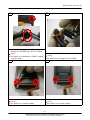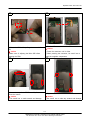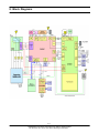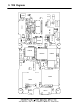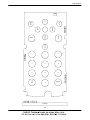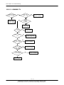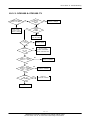
1
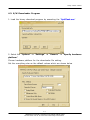
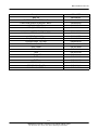
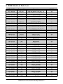
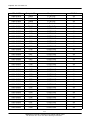
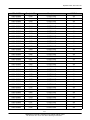
GSM TELEPHONE
SGH-E210
GSM TELEPHONE
CONTENTS
1.
Safety Precautions
2.
Specification
3.
Product Function
4.
Array course control
5.
Exploded View and Parts List
6.
MAIN Electrical Parts List
7.
Block Diagrams
8.
PCB Diagrams
9.
Flow Chart of Troubleshooting
10.
Reference data
GSPN (Global Service Partner Network)
Country
Web Site
North America
service.samsungportal.com
Latin America
latin.samsungportal.com
CIS
cis.samsungportal.com
Europe
europe.samsungportal.com
China
china.samsungportal.com
Asia
asia.samsungportal.com
Mideast & Africa
mea.samsungportal.com
This Service Manual is a property of Samsung Electronics Co.,Ltd.
Any unauthorized use of Manual can be punished under applicable
International and/or domestic law.
ⓒ Samsung Electronics Co.,Ltd.
2007. 08. Rev.1.0
1. Safety Precautions
1-1. Repair Precaution
● Repair in Shield Box, during detailed tuning.
Take specially care of tuning or test,
because specipicty of cellular phone is sensitive for surrounding interference(RF noise).
● Be careful to use a kind of magnetic object or tool,
because performance of parts is damaged by the influence of manetic force.
● Surely use a standard screwdriver when you disassemble this product,
otherwise screw will be worn away.
● Use a thicken twisted wire when you measure level.
A thicken twisted wire has low resistance, therefore error of measurement is few.
● Repair after separate Test Pack and Set because for short danger (for example an
overcurrent and furious flames of parts etc) when you repair board in condition of
connecting Test Pack and tuning on.
● Take specially care of soldering, because Land of PCB is small and weak in heat.
● Surely tune on/off while using AC power plug, because a repair of battery charger is
dangerous when tuning ON/OFF PBA and Connector after disassembing charger.
● Don't use as you pleases after change other material than replacement registered on SEC
System. Otherwise engineer in charge isn't charged with problem that you don't keep this
rules.
1-1
SAMSUNG Proprietary-Contents may change without notice
This Document can not be used without Samsung's authorization
Safety Precautions
1-2. ESD(Electrostatically Sensitive Devices) Precaution
Several semiconductor may be damaged easilly by static electricity. Such parts are called by
ESD(Electrostatically Sensitive Devices), for example IC,BGA chip etc. Read Precaution below.
You can prevent from ESD damage by static electricity.
● Remove static electricity remained your body before you touch semiconductor or parts with
semiconductor. There are ways that you touch an earthed place or wear static electricity
prevention string on wrist.
● Use earthed soldering steel when you connect or disconnect ESD.
● Use soldering removing tool to break static electricity. , otherwise ESD will be damaged by
static electricity.
● Don't unpack until you set up ESD on product. Because most of ESD are packed by box
and aluminum plate to have conductive power,they are prevented from static electricity.
● You must maintain electric contact between ESD and place due to be set up until ESD is
connected completely to the proper place or a circuit board.
1-2
SAMSUNG Proprietary-Contents may change without notice
This Document can not be used without Samsung's authorization
2. Specification
2-1. GSM General Specification
GSM 90 0
DCS1800
PCS1900
F req . Ba nd[MHz]
Uplink/Downlin k
880~91 5
925~96 0
1 710~17 85
1 805~18 80
1850~1 910
1930~1 990
ARF CN r ange
0~124
& 975~1 023
512~88 5
512~8 10
T x/Rx spacing
45MHz
95MHz
80MHz
Mod. Bit r ate /
Bit Period
270 .833Kbps
3.692 us
270 .833Kbps
3.692 us
27 0.833 Kbps
3.69 2us
Ti me Slo t Pe rio d
/Frame Period
576.9 us
4. 615ms
576.9 us
4. 615ms
576. 9us
4 .615ms
Modulatio n
0.3G M SK
0.3G MSK
0.3G M SK
MS Po wer
3 3dBm~5 dBm
3 0dBm~0 dBm
3 0dBm~0 dBm
Power L evel
5pcl~19pcl
0pcl~15pcl
0pcl~15pcl
Sensit ivit y
-1 02dBm
-1 00dBm
- 102dBm
TDMA M ux
8
8
8
Ce ll Radius
35Km
2Km
2Km
2-1
Speclflcation
2-2. GSM Tx Power Class
TX Power
control level
GSM900
TX Power
control
level
DCS1800
TX Power
control
level
PCS1900
5
33±2dBm
0
30±2dBm
0
30±2dBm
6
31±3dBm
1
28±3dBm
1
28±3dBm
7
29±3dBm
2
26±3dBm
2
26±3dBm
8
27±3dBm
3
24±3dBm
3
24±3dBm
9
25±3dBm
4
22±3dBm
4
22±3dBm
10
23±3dBm
5
20±3dBm
5
20±3dBm
11
21±3dBm
6
18±3dBm
6
18±3dBm
12
19±3dBm
7
16±3dBm
7
16±3dBm
13
17±3dBm
8
14±3dBm
8
14±3dBm
14
15±3dBm
9
12±4dBm
9
12±4dBm
15
13±3dBm
10
10±4dBm
10
10±4dBm
16
11±5dBm
11
8±4dBm
11
8±4dBm
17
9±5dBm
12
6±4dBm
12
6±4dBm
18
7±5dBm
13
4±4dBm
13
4±4dBm
19
5±5dBm
14
2±5dBm
14
2±5dBm
15
0±5dBm
15
0±5dBm
2-2
3. Product Function
Main Function
- Camera and camcorder
- Music player
- FM radio
- Offlime mode
- Bluetooth
- Web browser
- Multimedia Message Service(MMS)
- SOS message
- Organiser
-
3-1
SAMSUNG Proprietary-Contents may change without notice
This Document can not be used without Samsung's authorization
4. Array course control
Test Jig (GH80-03312A)
Test Cable (GH39-00830A)
RF Test Cable (GH39-00397A)
4-1
SAMSUNG Proprietary-Contents may change without notice
This Document can not be used without Samsung's authorization
Array course control
Software Downloading
4-1. Downloading Binary Files
• Three binary files for downloading SGH-E210.
– E210XXYY.s3 : Main source code binary.
4-2. Pre-requsite for Downloading
• Downloader Program(OptiFlash.exe)
• E210 Mobile Phone
• Data Cable
• Binary files
4-2
SAMSUNG Proprietary-Contents may change without notice
This Document can not be used without Samsung's authorization
Array course control
4-3. S/W Downloader Program
1. Load the binary download program by executing the “OptiFlash.exe”
2. Select the “Options” -> “Settings” -> “Generic” -> “Specify hardware
platform”.
Choose hardware platform for the downloader file setting.
Set the everything else as the default values which are shown below
4-3
SAMSUNG Proprietary-Contents may change without notice
This Document can not be used without Samsung's authorization
Array course control
3. Select the COM port when the download cable is connected
Up to 64 ports are supported. Additionally you can select the maximum
transfer speed OptiFlash will use to communicate with the phone.
However, OptiFlash will use a slower speed if either the PC’s or the
phone’s serial hardware is incapable of handling the selected speed
4-4
SAMSUNG Proprietary-Contents may change without notice
This Document can not be used without Samsung's authorization
Array course control
4. Select the“Flash&Verify” -> “Browse”
Set the directory path and choose the latest s/w binary, for example
“E210XXYY.s3”, for the downloader binary setting.
Make sure that not to change the reserved memory
regions.
In case of E210 the reserved memory regions are :
-0x23c00000 ~ 0x23ffffff
4-5
SAMSUNG Proprietary-Contents may change without notice
This Document can not be used without Samsung's authorization
Array course control
5. Click “OK” button then press “Flash”.
(Before pressing ‘Flash’ button, push the button ‘*’and ‘END’ at the same
time. Then press ‘Flash’.)
Downloader will upload the binary file as below for the downloading.
6. When downloading is finished successfully, there is a “All is well”
message.
7. After finishing downloading, Certain memory resets should be done to
guarantee the normal performance.
8. Confirm the downloaded version name and etc. :
*#1234#
Full Reset :
*2767*3855#
4-6
SAMSUNG Proprietary-Contents may change without notice
This Document can not be used without Samsung's authorization
5. Exploded View and Parts List
5-1. Cellular phone Exploded View
QKP01
QIF01
QCK01
QFR01
QFU01
QVO01
QSD01
QCR71
QME16
QMI03
QMP01
QMO01
QLC01
QSP01
QME01
QMI01
QAN11
QMW01
QSH01
QCA01
QSP05
QAN02
QFL01
QHI01
QRE01
QCR05
QSC04
QRF01
QCR54
QBA01
QBA00
5-1
SAMSUNG Proprietary-Contents may change without notice
This Document can not be used without Samsung's authorization
Main Electrical Parts List
5-2. Cellular phone Parts list
Design LOC
Discription
SEC CODE
QAN11
ASSY-CUSHION-CUSHION RUBBER IN
GH98-01077A
QBA00
ASSY COVER-BATT
GH98-05107A
QBA01
INNER BATTERY PACK-800MAH,MAIN
GH43-02589A
QCA01
CAMERA MODULE-SGHE210
GH59-04657A
QCR05
SCREW-MACHINE
6001-001478
QCR54
SCREW-MACHINE
6001-001645
QCR71
SCREW-MACHINE
6001-002095
QFU01
ASSY CASE-FOLDER UPPER
GH98-03571A
QKP01
ASSY KEYPAD-MAIN(XEN/ZK)
GH98-05104A
QME01
DOME SHEET-SGHE210 TF DOME SHE
GH59-04560A
QME16
ASSY ETC-SGHE210 CON TO CON
GH59-04024A
QMI01
MICROPHONE-ASSY-SGHE210
GH30-00408A
QMI03
RMO-MIC HOLDER
GH73-05342A
QMO01
MOTOR BLOWER-SCHA530 MOTOR
GH31-00047A
QMP01
PBA MAIN-SGHE210
GH92-03388A
QMW01
ASSY COVER-MAIN WINDOW
GH98-05105A
QSC04
TAPE-SCREW SHEET
GH74-32473A
QSH01
IPR COVER-SHIELD
GH70-02471A
QSP01
SPEAKER
3001-002188
QRF01
TAPE-RF SHEET
GH74-32474A
QLC01
ELA UNIT-SGHE210 LCD MODULE SV
GH96-02766A
QFL01
ASSY CASE-FOLDER LOWER
GH98-03572A
QHI01
ASSY MEC-HINGE
GH75-09605A
QSP05
ASSY DECO-SPK IN
GH98-05106A
QRE01
ASSY CASE-REAR
GH98-03574A
QAN02
INTENNA-SGHE210
GH42-01145A
QFR01
ASSY CASE-FRONT
GH98-03573A
QCK01
PMO KEY-CAMERA
GH72-42023A
QIF01
PMO COVER-IF
GH72-42196A
QSD01
PMO COVER-MICRO SD
GH72-42157A
QVO01
PMO KEY-VOLUME
GH72-42160A
5-2
SAMSUNG Proprietary-Contents may change without notice
This Document can not be used without Samsung's authorization
Main Electrical Parts List
Discription
SEC CODE
BAG PE
6902-000297
ADAPTOR-ATADS10EBE,BLK,EU
GH44-01702A
EARPHONE-SGHE210,HEADSET,BLK,A
GH59-04535A
LABEL(P)-UNIT SEAL
GH68-00518B
LABEL(R)-WATER SOAK
GH68-09361A
MANUAL USERS-EU ENGLISH
GH68-13874A
MANUAL USERS-EU PORTUGUESE
GH68-13884A
LABEL(R)-MAIN(EU)
GH68-13957A
BOX(P)-UNIT MAIN(EU)
GH69-05052A
CUSHION-CASE TA2 MA2
GH69-05053A
MPR-REMOVE TAPE LCD
GH74-13804A
TAPE GASK
GH74-31842A
TAPE INSU
GH74-32033A
TAPE
GH74-33512A
TAPE-LOWER
GH74-33601A
TAPE
GH74-33602A
TAPE
GH74-33809A
TAPE GASK
GH74-33810A
SPONGE-SOUND LCD
GH74-33913A
VINYL-BOHO UPPER 2
GH74-34251A
5-3
SAMSUNG Proprietary-Contents may change without notice
This Document can not be used without Samsung's authorization
6. MAIN Electrical Parts List
SEC CODE
Design LOC
Discription
STATUS
GH71-06262A
ANT100
NPR-ANTENNA CONTACT V2
SA
GH71-06262A
ANT101
NPR-ANTENNA CONTACT V2
SA
GH13-00044A
UCD301
IC ASIC-SGHE490
SA
4709-001422
MOD101
BLUETOOTH MODULE
SA
4302-001130
BAT300
BATTERY-LI(2ND)
SA
4202-001325
ANT102
ANTENNA-CHIP
SA
3711-006228
BTC400
HEADER-BATTERY
SA
3711-006015
HEA400
HEADER-BOARD TO BOARD
SA
3710-002499
IFC400
SOCKET-INTERFACE
SA
3709-001392
CN201
CONNECTOR-CARD EDGE
SA
3709-001384
SIM200
CONNECTOR-CARD EDGE
SA
3705-001358
RFS100
CONNECTOR-COAXIAL
SA
3404-001152
TAC400
SWITCH-TACT
SA
3404-001152
TAC401
SWITCH-TACT
SA
3404-001152
TAC402
SWITCH-TACT
SA
3301-001912
L109
BEAD-SMD
SA
3301-001120
L400
BEAD-SMD
SA
3301-001120
L401
BEAD-SMD
SA
2904-001600
F103
FILTER-SAW
SA
2904-001599
F102
FILTER-SAW
SA
2904-001592
F101
FILTER-SAW
SA
2801-004466
OSC301
CRYSTAL-SMD
SA
2801-004455
OSC100
CRYSTAL-SMD
SA
2801-004340
OSC300
CRYSTAL-SMD
SA
2703-003196
L500
INDUCTOR-SMD
SA
2703-002910
L101
INDUCTOR-SMD
SA
2703-002906
L102
INDUCTOR-SMD
SA
2703-002906
L104
INDUCTOR-SMD
SA
2703-002900
L106
INDUCTOR-SMD
SA
2703-002782
L300
INDUCTOR-SMD
SA
2703-002603
L103
INDUCTOR-SMD
SA
2703-002603
L105
INDUCTOR-SMD
SA
2703-002485
L100
INDUCTOR-SMD
SA
2703-002208
L108
INDUCTOR-SMD
SA
2703-002207
L107
INDUCTOR-SMD
SA
2404-001484
TA401
C-TA,CHIP
SA
2404-001484
TA402
C-TA,CHIP
SA
6-1
SAMSUNG Proprietary-Contents may change without notice
This Document can not be used without Samsung's authorization
Exploded View and Parts List
SEC CODE
Design LOC
Discription
STATUS
2404-001414
TA403
C-TA,CHIP
SA
2404-001414
TA404
C-TA,CHIP
SA
2404-001406
TA400
C-TA,CHIP
SA
2404-001381
TA405
C-TA,CHIP
SA
2404-001381
TA406
C-TA,CHIP
SA
2203-006979
C235
C-CER,CHIP
SA
2203-006838
C126
C-CER,CHIP
SA
2203-006838
C127
C-CER,CHIP
SA
2203-006838
C215
C-CER,CHIP
SA
2203-006838
C314
C-CER,CHIP
SA
2203-006838
C349
C-CER,CHIP
SA
2203-006838
C350
C-CER,CHIP
SA
2203-006838
C351
C-CER,CHIP
SA
2203-006648
C116
C-CER,CHIP
SA
2203-006648
C466
C-CER,CHIP
SA
2203-006648
C467
C-CER,CHIP
SA
2203-006585
C400
C-CER,CHIP
SA
2203-006585
C401
C-CER,CHIP
SA
2203-006562
C128
C-CER,CHIP
SA
2203-006562
C132
C-CER,CHIP
SA
2203-006562
C134
C-CER,CHIP
SA
2203-006562
C135
C-CER,CHIP
SA
2203-006562
C223
C-CER,CHIP
SA
2203-006562
C313
C-CER,CHIP
SA
2203-006562
C317
C-CER,CHIP
SA
2203-006562
C328
C-CER,CHIP
SA
2203-006562
C331
C-CER,CHIP
SA
2203-006562
C340
C-CER,CHIP
SA
2203-006562
C341
C-CER,CHIP
SA
2203-006562
C342
C-CER,CHIP
SA
2203-006562
C343
C-CER,CHIP
SA
2203-006562
C344
C-CER,CHIP
SA
2203-006562
C345
C-CER,CHIP
SA
2203-006562
C346
C-CER,CHIP
SA
2203-006562
C347
C-CER,CHIP
SA
2203-006562
C348
C-CER,CHIP
SA
2203-006562
C368
C-CER,CHIP
SA
6-2
SAMSUNG Proprietary-Contents may change without notice
This Document can not be used without Samsung's authorization
Exploded View and Parts List
SEC CODE
Design LOC
Discription
STATUS
2203-006562
C370
C-CER,CHIP
SA
2203-006562
C372
C-CER,CHIP
SA
2203-006562
C404
C-CER,CHIP
SA
2203-006562
C405
C-CER,CHIP
SA
2203-006562
C406
C-CER,CHIP
SA
2203-006562
C450
C-CER,CHIP
SA
2203-006562
C460
C-CER,CHIP
SA
2203-006562
C473
C-CER,CHIP
SA
2203-006556
C104
C-CER,CHIP
SA
2203-006556
C200
C-CER,CHIP
SA
2203-006474
C316
C-CER,CHIP
SA
2203-006423
C113
C-CER,CHIP
SA
2203-006423
C117
C-CER,CHIP
SA
2203-006423
C118
C-CER,CHIP
SA
2203-006423
C119
C-CER,CHIP
SA
2203-006423
C129
C-CER,CHIP
SA
2203-006423
C202
C-CER,CHIP
SA
2203-006423
C204
C-CER,CHIP
SA
2203-006423
C206
C-CER,CHIP
SA
2203-006423
C207
C-CER,CHIP
SA
2203-006423
C208
C-CER,CHIP
SA
2203-006423
C211
C-CER,CHIP
SA
2203-006423
C212
C-CER,CHIP
SA
2203-006423
C233
C-CER,CHIP
SA
2203-006423
C300
C-CER,CHIP
SA
2203-006423
C301
C-CER,CHIP
SA
2203-006423
C302
C-CER,CHIP
SA
2203-006423
C303
C-CER,CHIP
SA
2203-006423
C338
C-CER,CHIP
SA
2203-006423
C367
C-CER,CHIP
SA
2203-006423
C373
C-CER,CHIP
SA
2203-006361
C122
C-CER,CHIP
SA
2203-006361
C334
C-CER,CHIP
SA
2203-006361
C339
C-CER,CHIP
SA
2203-006318
C105
C-CER,CHIP
SA
2203-006318
C108
C-CER,CHIP
SA
2203-006318
C109
C-CER,CHIP
SA
6-3
SAMSUNG Proprietary-Contents may change without notice
This Document can not be used without Samsung's authorization
Exploded View and Parts List
SEC CODE
Design LOC
Discription
STATUS
2203-006318
C110
C-CER,CHIP
SA
2203-006318
C112
C-CER,CHIP
SA
2203-006260
C130
C-CER,CHIP
SA
2203-006257
C318
C-CER,CHIP
SA
2203-006194
C114
C-CER,CHIP
SA
2203-006194
C115
C-CER,CHIP
SA
2203-006194
C209
C-CER,CHIP
SA
2203-006194
C234
C-CER,CHIP
SA
2203-006194
C319
C-CER,CHIP
SA
2203-006194
C320
C-CER,CHIP
SA
2203-006194
C321
C-CER,CHIP
SA
2203-006194
C374
C-CER,CHIP
SA
2203-006183
C220
C-CER,CHIP
SA
2203-006048
C305
C-CER,CHIP
SA
2203-005792
C100
C-CER,CHIP
SA
2203-005792
C103
C-CER,CHIP
SA
2203-005736
C101
C-CER,CHIP
SA
2203-005736
C106
C-CER,CHIP
SA
2203-005736
C111
C-CER,CHIP
SA
2203-005736
C123
C-CER,CHIP
SA
2203-005736
C222
C-CER,CHIP
SA
2203-005731
C102
C-CER,CHIP
SA
2203-005725
C441
C-CER,CHIP
SA
2203-005725
C442
C-CER,CHIP
SA
2203-005725
C443
C-CER,CHIP
SA
2203-005683
C438
C-CER,CHIP
SA
2203-005683
C439
C-CER,CHIP
SA
2203-005683
C440
C-CER,CHIP
SA
2203-005683
C448
C-CER,CHIP
SA
2203-005682
C107
C-CER,CHIP
SA
2203-005682
C120
C-CER,CHIP
SA
2203-005682
C121
C-CER,CHIP
SA
2203-005682
C124
C-CER,CHIP
SA
2203-005682
C125
C-CER,CHIP
SA
2203-005682
C407
C-CER,CHIP
SA
2203-005682
C408
C-CER,CHIP
SA
2203-005682
C409
C-CER,CHIP
SA
6-4
SAMSUNG Proprietary-Contents may change without notice
This Document can not be used without Samsung's authorization
Exploded View and Parts List
SEC CODE
Design LOC
Discription
STATUS
2203-005682
C410
C-CER,CHIP
SA
2203-005682
C411
C-CER,CHIP
SA
2203-005682
C412
C-CER,CHIP
SA
2203-005682
C413
C-CER,CHIP
SA
2203-005682
C414
C-CER,CHIP
SA
2203-005682
C415
C-CER,CHIP
SA
2203-005682
C416
C-CER,CHIP
SA
2203-005682
C417
C-CER,CHIP
SA
2203-005682
C418
C-CER,CHIP
SA
2203-005682
C419
C-CER,CHIP
SA
2203-005682
C420
C-CER,CHIP
SA
2203-005682
C421
C-CER,CHIP
SA
2203-005682
C422
C-CER,CHIP
SA
2203-005682
C423
C-CER,CHIP
SA
2203-005682
C424
C-CER,CHIP
SA
2203-005682
C425
C-CER,CHIP
SA
2203-005682
C426
C-CER,CHIP
SA
2203-005682
C427
C-CER,CHIP
SA
2203-005682
C430
C-CER,CHIP
SA
2203-005682
C431
C-CER,CHIP
SA
2203-005682
C432
C-CER,CHIP
SA
2203-005682
C433
C-CER,CHIP
SA
2203-005682
C434
C-CER,CHIP
SA
2203-005682
C435
C-CER,CHIP
SA
2203-005682
C436
C-CER,CHIP
SA
2203-005682
C437
C-CER,CHIP
SA
2203-005682
C444
C-CER,CHIP
SA
2203-005682
C445
C-CER,CHIP
SA
2203-005552
C131
C-CER,CHIP
SA
2203-005483
C454
C-CER,CHIP
SA
2203-005483
C462
C-CER,CHIP
SA
2203-005483
C464
C-CER,CHIP
SA
2203-005483
C474
C-CER,CHIP
SA
2203-005482
C136
C-CER,CHIP
SA
2203-005482
C137
C-CER,CHIP
SA
2203-005482
C224
C-CER,CHIP
SA
2203-005482
C225
C-CER,CHIP
SA
6-5
SAMSUNG Proprietary-Contents may change without notice
This Document can not be used without Samsung's authorization
Exploded View and Parts List
SEC CODE
Design LOC
Discription
STATUS
2203-005482
C228
C-CER,CHIP
SA
2203-005482
C371
C-CER,CHIP
SA
2203-005482
C476
C-CER,CHIP
SA
2203-005050
C140
C-CER,CHIP
SA
2203-002709
C214
C-CER,CHIP
SA
2203-002709
C221
C-CER,CHIP
SA
2203-002709
C232
C-CER,CHIP
SA
2203-002709
C315
C-CER,CHIP
SA
2203-002709
C472
C-CER,CHIP
SA
2203-001072
C310
C-CER,CHIP
SA
2203-001072
C311
C-CER,CHIP
SA
2203-000940
C227
C-CER,CHIP
SA
2203-000812
C226
C-CER,CHIP
SA
2203-000812
C229
C-CER,CHIP
SA
2203-000812
C230
C-CER,CHIP
SA
2203-000812
C428
C-CER,CHIP
SA
2203-000812
C429
C-CER,CHIP
SA
2203-000550
C357
C-CER,CHIP
SA
2203-000550
C358
C-CER,CHIP
SA
2203-000438
C402
C-CER,CHIP
SA
2203-000438
C403
C-CER,CHIP
SA
2203-000330
C329
C-CER,CHIP
SA
2203-000330
C330
C-CER,CHIP
SA
2203-000311
C456
C-CER,CHIP
SA
2203-000311
C457
C-CER,CHIP
SA
2203-000311
C459
C-CER,CHIP
SA
2203-000254
C213
C-CER,CHIP
SA
2203-000254
C216
C-CER,CHIP
SA
2203-000254
C337
C-CER,CHIP
SA
2203-000233
C133
C-CER,CHIP
SA
2203-000233
C231
C-CER,CHIP
SA
2203-000189
C471
C-CER,CHIP
SA
2007-009115
R315
R-CHIP
SA
2007-009084
R318
R-CHIP
SA
2007-008816
R227
R-CHIP
SA
2007-008816
R228
R-CHIP
SA
2007-008809
R308
R-CHIP
SNA
6-6
SAMSUNG Proprietary-Contents may change without notice
This Document can not be used without Samsung's authorization
Exploded View and Parts List
SEC CODE
Design LOC
Discription
STATUS
2007-008774
R259
R-CHIP
SA
2007-008579
R257
R-CHIP
SA
2007-008531
R266
R-CHIP
SA
2007-008531
R319
R-CHIP
SA
2007-008516
R243
R-CHIP
SA
2007-008483
R102
R-CHIP
SA
2007-008483
R105
R-CHIP
SA
2007-008483
R412
R-CHIP
SA
2007-008478
R248
R-CHIP
SA
2007-008420
R250
R-CHIP
SA
2007-008420
R252
R-CHIP
SA
2007-008419
R414
R-CHIP
SA
2007-008419
R416
R-CHIP
SA
2007-008419
R417
R-CHIP
SA
2007-008419
R418
R-CHIP
SA
2007-008055
R103
R-CHIP
SA
2007-008055
R104
R-CHIP
SA
2007-008055
R320
R-CHIP
SA
2007-008045
R425
R-CHIP
SA
2007-007741
R100
R-CHIP
SA
2007-007741
R101
R-CHIP
SA
2007-007314
R305
R-CHIP
SA
2007-007308
R304
R-CHIP
SA
2007-007190
R404
R-CHIP
SA
2007-007190
R405
R-CHIP
SA
2007-002965
R407
R-CHIP
SA
2007-002965
R409
R-CHIP
SA
2007-002965
R429
R-CHIP
SA
2007-002965
R430
R-CHIP
SA
2007-001288
R426
R-CHIP
SA
2007-001288
R427
R-CHIP
SA
2007-001288
R428
R-CHIP
SA
2007-000775
R400
R-CHIP
SA
2007-000775
R401
R-CHIP
SA
2007-000242
R410
R-CHIP
SA
2007-000242
R415
R-CHIP
SA
2007-000242
R419
R-CHIP
SA
6-7
SAMSUNG Proprietary-Contents may change without notice
This Document can not be used without Samsung's authorization
Exploded View and Parts List
SEC CODE
Design LOC
Discription
STATUS
2007-000242
R422
R-CHIP
SA
2007-000173
R406
R-CHIP
SA
2007-000173
R408
R-CHIP
SA
2007-000170
R261
R-CHIP
SA
2007-000170
R402
R-CHIP
SA
2007-000170
R403
R-CHIP
SA
2007-000168
R246
R-CHIP
SA
2007-000162
R256
R-CHIP
SA
2007-000157
R247
R-CHIP
SA
2007-000153
R413
R-CHIP
SA
2007-000153
R421
R-CHIP
SA
2007-000148
R267
R-CHIP
SA
2007-000138
R411
R-CHIP
SA
2007-000138
R420
R-CHIP
SA
1405-001082
V200
VARISTOR
SA
1405-001082
VR400
VARISTOR
SA
1405-001082
VR401
VARISTOR
SA
1405-001082
VR403
VARISTOR
SA
1405-001082
VR404
VARISTOR
SA
1405-001082
VR405
VARISTOR
SA
1404-001165
TH300
THERMISTOR-NTC
SA
1205-003224
UCP200
IC-DATA COMM./GEN.
SA
1205-003116
UCD101
IC-TRANSCEIVER
SA
1205-002272
U204
IC-TRANSCEIVER
SA
1204-002746
U100
IC-TUNER
SA
1203-004763
U205
IC-VOL. DETECTOR
SA
1203-004663
UCD300
IC-POWER SUPERVISOR
SA
1201-002304
U407
IC-AUDIO AMP
SA
1201-002278
PAM100
IC-POWER AMP
SA
1108-000046
UME200
IC-MCP
SA
1009-001035
U202
IC-HALL EFFECT S/W
SA
1001-001405
U400
IC-ANALOG MULTIPLEX
SA
1001-001405
U408
IC-ANALOG MULTIPLEX
SA
0601-002268
LED400
LED
SA
0601-002268
LED401
LED
SA
0601-002268
LED402
LED
SA
0406-001254
ZD404
DIODE-TVS
SA
6-8
SAMSUNG Proprietary-Contents may change without notice
This Document can not be used without Samsung's authorization
Exploded View and Parts List
SEC CODE
Design LOC
Discription
STATUS
0406-001254
ZD405
DIODE-TVS
SA
0406-001241
U401
DIODE-TVS
SA
0406-001241
U402
DIODE-TVS
SA
0406-001241
U403
DIODE-TVS
SA
0406-001241
U404
DIODE-TVS
SA
0406-001241
U405
DIODE-TVS
SA
0406-001241
U406
DIODE-TVS
SA
0406-001237
U201
DIODE-TVS
SNA
0403-001547
ZD402
DIODE-ZENER
SA
0403-001547
ZD403
DIODE-ZENER
SA
0403-001427
ZD406
DIODE-ZENER
SA
6-9
SAMSUNG Proprietary-Contents may change without notice
This Document can not be used without Samsung's authorization
7. Disassembly and Assembly Instructions
7-1. Disassembly
2
1
1) Unscrew 4 screws.
※ caution
※ caution
1) Remove battery and SIM card.
1) Be careful not to scratch molding.
4
3
1) Separate LCD CONNECTOR from the PBA
1)Lift up the REAR CASE and separate it from the
using tweezers.
FRONT.
※ caution
※ caution
1) Be careful not to damage the components
around LCD CONNECTOR.
1) Be careful not to damage LOCKER.
7-1
SAMSUNG Proprietary-Contents may change without notice
This Document can not be used without Samsung's authorization
Exploded View and Parts List
6
5
1) Slowly separate the PBA from the keypad using
tweezers.
※ caution
1) Be careful not to damage double-faced tape on
the keypad.
1) Lift up the PBA by pushing the keypad.
2) Be careful not to damage the DOPARO SHEET
※ caution
1) Be careful not to damage the FRONT molding.
(light guide film) .
8
7
1) Remove the keypad from the ass'y.
※ caution
1) Remove the black tape with tweezers.
1) Be careful not to damage double-faced tape on ※ caution
1) Be careful not to damage the LCD FPCB.
the keypad.
7-2
SAMSUNG Proprietary-Contents may change without notice
This Document can not be used without Samsung's authorization
Exploded View and Parts List
10
9
1) Push the Hinge with tweezers(Top view) and
separate the FOLDER Ass'y from the FRONT.
※ caution
1) Separate the FOLDER Ass'y from the FRONT.
1) Be careful not to damage the FRONT molding
and the Hinge.
※ caution
11
12
1) Remove the two screw sheets.
1) Unscrew at two points.
※ caution
1) Be careful not to damage the LCD FPCB.
※ caution
1) Be careful not to scratch molding.
1) Be careful not to scratch molding.
7-3
SAMSUNG Proprietary-Contents may change without notice
This Document can not be used without Samsung's authorization
Exploded View and Parts List
14
13
1) Open the locker between the FOLDED
UPPER and the FOLDER LOWER.
1) Separate the UPPER and the LOWER.
※ caution
※ caution
1) Be careful not to scratch molding.
1) Be careful not to damage LOCKER and molding
15
16
1) Using tweezers, separate the SPEAKER from
the FOLDER LOWER.
2) Do for the MOTOR in the same way.
※ caution
1) Be careful not to damage thePEAKER/MOTOR
and wires.
1) Open the camera connector with tweezers.
1) Separate the CAMERA from the FOLDER
LOWER using tweezers.
※ caution
1) Be careful not to damage components around
the connector.
2) Be careful not to damage the CAMERA
MODULE.
7-4
SAMSUNG Proprietary-Contents may change without notice
This Document can not be used without Samsung's authorization
Exploded View and Parts List
18
17
1) Bend the LOWER slightly and separate the LCD
and the LOWER.
1) Separate the LCD FPCB from the LOWER.
※ caution
※ caution
1) Do not touch LCD GLASS with your hands.
1)
Be careful not to damage the LCD FPCB.
19
1) Completed.
※ caution
1) Be careful not to leave any foreign substance
or fingerprint on the SUB-LCD.
7-5
SAMSUNG Proprietary-Contents may change without notice
This Document can not be used without Samsung's authorization
Exploded View and Parts List
7-2. Assembly
1
1)
※
1)
or
2
LCD Ass'y
caution
Be careful not to leave any foreign substance
fingerprint on the SUB-LCD.
1) Insert the LCD FPCB into the hole on the
LOWER carefully
※ caution
1)Be careful not to damage the FPCB.
4
3
1) Put the LCD Ass'y into place as shown.
1) Put the camera into place.
2) Put the speaker and motor into place.
2) As shown,put the connector until it clicks
※ caution
※ caution
1) Adjust a tape before putting the LCD.
1) Be careful not to touch the camera lens.
2) Be careful not to break wires.
2) Press the connector until it clicks.
7-6
SAMSUNG Proprietary-Contents may change without notice
This Document can not be used without Samsung's authorization
Exploded View and Parts List
6
5
1) Assembling the FOLDER should be done in
regular sequence as shown.(TOP-> BOTH SIDES
OF THE LCD ->BOTH SIDES OF THE SUB-LCD→
BOTTOM)
1) Tighten 2 screws.
※ caution
※ caution
1) Check if there are not any foreign substance.
2) Be careful not to make scratch and damage.
1) Be careful not to make scratch and damage.
7
8
1) Put up screw sheets.
※ caution
1) Be careful not to make scratch and damage.
1) Insert the FPCB of the FOLDER ASS'Y
assembled.
※ caution
1)
Be careful not to make scratch and damage.
7-7
SAMSUNG Proprietary-Contents may change without notice
This Document can not be used without Samsung's authorization
Exploded View and Parts List
10
9
1) Con To Con 에 0.3T 도전Tape를
부착한다.
1) Set the FRONT ASS'Y into the hole after
pressing the HINGE.
※ caution
1) Be careful not to make scratch and damage.
1) Put up the tape.
※ caution
11
12
1)As shown in the above picture, insert the upper
keypad first,and reverse the phone. Fit the lower
keypad in carefully by folding and unfolding it.
※ caution
1) Be careful not to fold the keypad.
1) The tape should not be on the FPCB.
1) Put the PBA in from inserting the upper PBA ,
as shown.
※ caution
1) Make sure of adjustng the right-side keys
(volume and camera keys) and left-side earphone
jack cover when putting the PBA in.
7-8
SAMSUNG Proprietary-Contents may change without notice
This Document can not be used without Samsung's authorization
Exploded View and Parts List
14
13
1) Press the PBA while pulling the cover of Micro
SD.
※ caution
1)Make sure of adjustng the Micro SD before
1) Fit the LCD connector into the PBA.
※ caution
1) Press the connector until it clicks.
2) When pressing the connector, be careful not to
pressing the PBA.
break the neighbor components.
15
16
1) Insert the top of the REAR carefully first, and
press the bottom.
※ caution
1) Be careful not to make scratch and damage.
1) Tighten 4 screws.
※ caution
1) Be careful not to make any scratch and damage
7-9
SAMSUNG Proprietary-Contents may change without notice
This Document can not be used without Samsung's authorization
8. Block Diagrams
8-1
SAMSUNG Proprietary-Contents may change without notice
This Document can not be used without Samsung's authorization
9. PCB Diagrams
U204
U401
U408
RFS100
U403
U407
VR400
IFC400
HEA400
F101
UCD301
U3 0 0
VR403
G1
UCD300
UCP200
TAC400
OSC100
G2
UME200
D301
TH300
TP401
TP200
BAT300
U405U406
U2 0 3
JCON201
MOD101
ANT102
U205
G202
V200
OSC301
G203
UCD1 0 1
U400
F102
O S C3 0 0
T A4 0 1
T A4 0 2
U100
ZD405ZD404
F103
TAC402
PAM100
U402TA404
TP101
ANT100
TAC401
ZD406 U404
ZD403
ANT101
U201
CN201
SIM200
TA403
VR404
VR405
G3
ZD401
TA400 ZD402
BTC400
MIC400
9-1
G201
G4
PCB Diagrams
LED400
PWR
CLEAR
SEND
RIGHT
I
DOWN
LEFT
STO
MENU
UP
U202
1
2
4
5
8
9
0
SHARP
TP214 TP215
TP212 TP211
TP213
TP210
TP209
TP217
JCON200
9-2
VR401
STAR
LED402
6
LED401
7
3
10. Flow Chart of Troubleshooting
10-1.Baseband
10-1-1. Power ON
'Power ON' Does not work
Check the current consumption
Check comsumption ≥ 100mA
NO
Down load again
YES
VBat ≥ 3.3V ?
NO
Charge the Battery
YES
C348 ≥ 1.8V ?
NO
Check UCD300 and C348
YES
C347 ≥ 2.9V?
NO
YES
C318≥2.9V?
NO
Check UCD301 and C318
YES
Check the clock signal
NO
at pin #3 of OSC100
Check the clock OSC100
Freq.=26MHz,Vrms ≥500mV
YES
NO
Check pin #8 of UCD101
Freq.=26MHz ?
Check the clock UCD101
YES
Check the Initial operation
END
10-1
SAMSUNG Proprietary-Contents may change without notice
This Document can not be used without Samsung's authorization
Flow Chart of Troubleshooting
10-1-2. Initial
Initial Failure
NO
The voltage at the C348=1.8V?
The voltage at the C347=2.9V?
Check the UCD300
(If it has some problem,
it has to be replaced.)
YES
The voltage at pin#4
NO
of U300 " Low --> High" ?
Check the UCD300
(If it has some problem,
it has to be replaced.)
YES
NO
There is 32.768KHz wave
form at the C329, C330 ?
Check the UCD300
YES
The voltage is 2.8V
NO
at the C346, C345?
Check the UCD300
YES
NO
LCD Display OK ?
Check the LCD module
YES
NO
Sound operation OK ?
Check the Audio part
YES
END
10-2
SAMSUNG Proprietary-Contents may change without notice
This Document can not be used without Samsung's authorization
Flow Chart of Troubleshooting
10-1-3. Sim Part
"Insert SIM" is displayed on the LCD
Sim socket checking
NO
"Is it inserted?"
Insert Simcard
YES
NO
The voltage is 2.8V at C227?
Check the UCD300
YES
Is there any signal
NO
pin C229, C230, C226?
Check the UCD300 & UCP200
YES
Check the SIM Card
END
10-3
SAMSUNG Proprietary-Contents may change without notice
This Document can not be used without Samsung's authorization
Flow Chart of Troubleshooting
10-1-4. LCD Display part
LCD display is abnormal
Check LCD connection
and replace LCD
LCD Backlight is on?
NO
pin#1 of FPCB02
YES
Check LCD
Check FPCB02
is high?
NO
YES
pin#2 of U401
YES
is high?
NO
C12 > 3.5V?
NO
Check C12
Recharge Bat.
YES
pin#6 of U01
NO
is high?
YES
CHeck U01
C444 is 2.9V?
NO
Check UCD300
YES
pin#5 of U403
NO
Check U301
is LOW?
YES
Are there anysignal
NO
at pin#3 of U403?
YES
Check U400
10-4
SAMSUNG Proprietary-Contents may change without notice
This Document can not be used without Samsung's authorization
Check UCP200
Flow Chart of Troubleshooting
10-1-5. Microphone Part
Micro-phone does not work
NO
Soldering OK?
Solder the microphone again
YES
Check the DC bias voltage on
Mic path.
NO
The voltage of C456 is
about 2.2V±10%?
Solder the microphone again
or Replace
R411, R410, R415
YES
NO
Is microphone OK?
Check UCD300
YES
END
10-5
SAMSUNG Proprietary-Contents may change without notice
This Document can not be used without Samsung's authorization
Flow Chart of Troubleshooting
10-1-6. Speaker Part
There is no sound from speaker.
Is the connection of HEA400 OK?
NO
Replace the Connection
or change speaker module
YES
Is there any signal
YES
Is there any signal
NO
at U408(#4,#6) ?
at R404, R405 ?
NO
YES
Check U408
Check UCD300
Change speaker module
END
10-6
SAMSUNG Proprietary-Contents may change without notice
This Document can not be used without Samsung's authorization
Flow Chart of Troubleshooting
10-1-7. Camera part
Camera function does not work
NO
Is the connect CN02 ok?
Connect the CN02
YES
NO
#40 of HEA400 IS HIGH?
Check UCD301
YES
Pin #1 of Q01 = 1.5V?
NO
YES
Pin #7 of Q01 IS HIGH?
Check
Q01
NO
YES
Check Bat.
Pin #6 of Q01 = 2.8V?
NO
YES
Pin#3 of OSC300 is 27MHz?
NO
Pin #7 of Q01 = High?
Q01
Check Bat.
Replace OSC300
NO
and check UCD301
YES
Is that clock signal at the
pin #12 of HEA400?
NO
YES
Pin#22 of HEA400 is High?
NO
Check
Check
UCD301
END
10-7
SAMSUNG Proprietary-Contents may change without notice
This Document can not be used without Samsung's authorization
Flow Chart of Troubleshooting
10-1-8. Mp3 part
There is no MP3 sound from Earphone
Is there any signal
at the pin #5,7 of IFC400?
YES
Replace the Earphone
NO
Is there any signal
at the pin #4,#16 of U400?
YES
Check & Replace TA401, TA402
NO
Is there any signal
at the R406, R408?
YES
Check U400
NO
Check UCD300
END
10-8
SAMSUNG Proprietary-Contents may change without notice
This Document can not be used without Samsung's authorization
Flow Chart of Troubleshooting
10-2. RF
10-2-1. GSM900/GSM1800/GSM1900 RX
Continuous RX ON
RF Input : 62 CH
AMP : -50dBm
NO
Pin #3 of OSC100
26MHz ?
Change or resolder OSC100
YES
Pin #12 of PAM100
No signal loss ?
NO
Change or resolder
C102, L102, L104
NO
Change or resolder
C101, PAM100(GSM)
C106, PAM100(DCS)
C111, PAM100(PCS)
YES
Pin #1 of
F101(G),F102(D),F103(P)
No signal loss ?
YES
Pin 21,22(G)#19,20(D)
#17,18(P) of UCD101
No signal loss ?
NO
Change or resolder
C100, C103, L100(GSM)
C105, C108, L103(DCS)
C110, C112, L105(PCS)
YES
Pin #4567 of UCD101
Any signal ?
NO
Change or resolder
UCD101
YES
Check UCD300
10-9
SAMSUNG Proprietary-Contents may change without notice
This Document can not be used without Samsung's authorization
Flow Chart of Troubleshooting
10-2-2. GSM900 TX
PAM100 Pin#12
About 2~3 dBm?
NO
C125 High,
C120 = Low?
YES
NO
UCD300,C120,C125
Check / Change
YES
RFS100, L101,
C102, L102,
C109, L104
Check / Change
PAM100
Pin#1
4~5dBm ?
NO
YES
PAM100
Check & Change
C122
= 3.7V?
NO
Check the
Battery Block
YES
PAM101 Pin #8
1.2V?
NO
R101, C123
Check & Resolder
Check UCD300 TXP
YES
UCD101 Check
Pin #13 >2.8V?
NO
C131, UCD300
Check or resolder
YES
UCD101 check
Pin#31 :26Mhz?
Vpp:1.2V
YES
UCD101 pin#7
any signal ?
NO
OSC100
Check & resolder
NO
UCD101
Check & resolder
YES
Change PAM100
10-10
SAMSUNG Proprietary-Contents may change without notice
This Document can not be used without Samsung's authorization
Flow Chart of Troubleshooting
10-2-3. DCS1800 & PCS1900 TX
PAM100 Pin#12
About 2~3 dBm?
NO
NO
PAM100
Pin#4, #5
High?
YES
UCD300,C120,C125
Check / Change
YES
RFS100, L101,
C102, L102,
C109, L104
Check / Change
PAM100
Pin#1
4~5dBm ?
NO
YES
PAM100
Check & Change
C122
= 3.7V?
NO
Check the
Battery Block
YES
PAM101
Pin #8
1.2V?
NO
R101, C123
Check & Resolder
Check UCD300 TXP
YES
UCD101 Check
Pin#13 ≥ 2.8V ?
NO
C131, UCD300
Check or resolder
YES
UCD101 Check
Pin #31 : 26MHz ?
Vpp : 1.2V?
NO
OSC100
Check & resolder
YES
UCD101
PIN #7
ANY SIGNAL?
NO
UCD101
Check & resolder
YES
Change PAM100
10-11
SAMSUNG Proprietary-Contents may change without notice
This Document can not be used without Samsung's authorization
11. Reference data
11-1. Reference Abbreviate
AAC: Advanced Audio Coding.
AVC : Advanced Video Coding.
BER : Bit Error Rate
BPSK: Binary Phase Shift Keying
CA : Conditional Access
CDM : Code Division Multiplexing
C/I : Carrier to Interference
DMB : Digital Multimedia Broadcasting
EN : European Standard
ES : Elementary Stream
ETSI: European Telecommunications Standards Institute
MPEG: Moving Picture Experts Group
PN : Pseudo-random Noise
PS : Pilot Symbol
QPSK: Quadrature Phase Shift Keying
RS : Reed-Solomon
SI : Service Information
TDM : Time Division Multiplexing
TS : Transport Stream
11-1
SAMSUNG Proprietary-Contents may change without notice
This Document can not be used without Samsung's authorization