1
To all our customers
Regarding the change of names mentioned in the document, such as
Hitachi Electric and Hitachi XX, to Renesas Technology Corp.
The semiconductor operations of Mitsubishi Electric and Hitachi were
transferred to Renesas Technology Corporation on April 1st 2003.
These operations include microcomputer, logic, analog and discrete devices,
and memory chips other than DRAMs (flash memory, SRAMs etc.)
Accordingly, although Hitachi, Hitachi, Ltd., Hitachi Semiconductors,
and other Hitachi brand names are mentioned in the document, these names
have in fact all been changed to Renesas Technology Corp.
Thank you for your understanding. Except for our corporate trademark,
logo and corporate statement, no changes whatsoever have been made to the
contents of the document, and these changes do not constitute any alteration
to the contents of the document itself.
Renesas Technology Home Page: www.renesas.com
Renesas Technology Corp.
Customer Support Dept.
April 1, 2003
Renesas Technology Corp.
Hitachi Single-Chip Microcomputer
H8/338 Series
H8/338
HD6473388, HD6433388, HD6413388
H8/337
HD6473378, HD6433378, HD6413378
H8/336
HD6433368
Hardware Manual
ADE-602-039B
Rev. 3.0
September 21, 1998
Hitachi Company or Division
Cautions
1. Hitachi neither warrants nor grants licenses of any rights of Hitachi’s or any third party’s
patent, copyright, trademark, or other intellectual property rights for information contained in
this document. Hitachi bears no responsibility for problems that may arise with third party’s
rights, including intellectual property rights, in connection with use of the information
contained in this document.
2. Products and product specifications may be subject to change without notice. Confirm that you
have received the latest product standards or specifications before final design, purchase or
use.
3. Hitachi makes every attempt to ensure that its products are of high quality and reliability.
However, contact Hitachi’s sales office before using the product in an application that
demands especially high quality and reliability or where its failure or malfunction may directly
threaten human life or cause risk of bodily injury, such as aerospace, aeronautics, nuclear
power, combustion control, transportation, traffic, safety equipment or medical equipment for
life support.
4. Design your application so that the product is used within the ranges guaranteed by Hitachi
particularly for maximum rating, operating supply voltage range, heat radiation characteristics,
installation conditions and other characteristics. Hitachi bears no responsibility for failure or
damage when used beyond the guaranteed ranges. Even within the guaranteed ranges,
consider normally foreseeable failure rates or failure modes in semiconductor devices and
employ systemic measures such as fail-safes, so that the equipment incorporating Hitachi
product does not cause bodily injury, fire or other consequential damage due to operation of
the Hitachi product.
5. This product is not designed to be radiation resistant.
6. No one is permitted to reproduce or duplicate, in any form, the whole or part of this document
without written approval from Hitachi.
7. Contact Hitachi’s sales office for any questions regarding this document or Hitachi
semiconductor products.
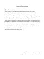
Preface
The H8/338 Series is a series of high-performance single-chip microcomputers having a fast
H8/300 CPU core and a set of on-chip supporting functions optimized for embedded control.
These include ROM, RAM, three types of timers, a serial communication interface, an A/D
converter, a D/A converter, I/O ports, and other functions needed in control system configurations,
so that compact, high-performance systems can be realized easily. The H8/338 Series includes
three chips: the H8/338 with 48K-byte ROM and 2K-byte RAM; the H8/337 with 32K-byte ROM
and 1K-byte RAM; and the H8/336 with 24K-byte ROM and 1K-byte RAM.
The H8/338 and H8/337 are available in a masked ROM version, a ZTAT*(Zero Turn-Around
Time) version, and a ROMless version, providing a quick and flexible response to conditions from
ramp-up through full-scale volume producion, even for applications with frequently-changing
specifications.
This manual describes the hardware of the H8/338 Series. Refer to the H8/300 Series
Programming Manual for a detailed description of the instruction set.
Note: ZTAT is a registered trademark of Hitachi, Ltd.
Rev. 3.0, 09/98, page i of viii
Contents
Section 1
1.1
1.2
1.3
Overview ...........................................................................................................
Overview ...........................................................................................................................
Block Diagram ..................................................................................................................
Pin Assignments and Functions.........................................................................................
1.3.1 Pin Arrangement ..................................................................................................
1.3.2 Pin Functions........................................................................................................
Section 2
2.1
2.2
2.3
2.4
2.5
2.6
2.7
CPU ....................................................................................................................
Overview ...........................................................................................................................
2.1.1 Features ................................................................................................................
Register Configuration ......................................................................................................
2.2.1 General Registers .................................................................................................
2.2.2 Control Registers..................................................................................................
2.2.3 Initial Register Values ..........................................................................................
Addressing Modes.............................................................................................................
2.3.1 Addressing Modes................................................................................................
2.3.2 How to Calculate Where the Excution Starts .......................................................
Data Formats .....................................................................................................................
2.4.1 Data Formats in General Registers.......................................................................
2.4.2 Memory Data Formats .........................................................................................
Instruction Set ...................................................................................................................
2.5.1 Data Transfer Instructions ....................................................................................
2.5.2 Arithmetic Operations ..........................................................................................
2.5.3 Logic Operations..................................................................................................
2.5.4 Shift Operations ...................................................................................................
2.5.5 Bit Manipulations.................................................................................................
2.5.6 Branching Instructions .........................................................................................
2.5.7 System Control Instructions .................................................................................
2.5.8 Block Data Transfer Instruction ...........................................................................
CPU States.........................................................................................................................
2.6.1 Program Execution State......................................................................................
2.6.2 Exception-Handling State ....................................................................................
2.6.3 Power-Down State................................................................................................
Access Timing and Bus Cycle...........................................................................................
2.7.1 Access to On-Chip Memory (RAM and ROM) ...................................................
2.7.2 Access to On-Chip Register Field and External Devices .....................................
Section 3
3.1
1
1
4
5
5
8
15
15
15
16
17
17
18
19
19
21
25
26
27
28
30
32
33
33
35
39
41
42
44
45
45
46
47
47
49
MCU Operating Modes and Address Space ........................................... 53
Overview ........................................................................................................................... 53
3.1.1 Mode Selection..................................................................................................... 53
3.1.2 Mode and System Control Registers (MDCR and SYSCR)................................. 54
Rev. 3.0, 09/98, page ii of viii
3.2
3.3
3.4
System Control Register (SYSCR)H'FFC4 ................................................................... 54
Mode Control Register (MDCR)H'FFC5 ...................................................................... 56
Address Space Map ........................................................................................................... 57
Section 4
4.1
4.2
4.3
4.4
Exception Handling........................................................................................
Overview ...........................................................................................................................
Reset ..................................................................................................................................
4.2.1 Overview ..............................................................................................................
4.2.2 Reset Sequence.....................................................................................................
4.2.3 Disabling of Interrupts after Reset .......................................................................
Interrupts ...........................................................................................................................
4.3.1 Overview ..............................................................................................................
4.3.2 Interrupt-Related Registers...................................................................................
4.3.3 External Interrupts................................................................................................
4.3.4 Internal Interrupts .................................................................................................
4.3.5 Interrupt Handling ................................................................................................
4.3.6 Interrupt Response Time ......................................................................................
4.3.7 Precaution.............................................................................................................
Note on Stack Handling.....................................................................................................
Section 5
5.1
5.2
5.3
Clock Pulse Generator ...................................................................................
Overview ...........................................................................................................................
5.1.1 Block Diagram .....................................................................................................
Oscillator Circuit ...............................................................................................................
System Clock Divider........................................................................................................
61
61
61
61
61
64
64
64
66
68
68
68
74
75
76
77
77
77
78
80
Section 6
6.1
6.2
6.3
6.4
6.5
6.6
6.7
6.8
6.9
6.10
I/O Ports ............................................................................................................ 81
Overview ........................................................................................................................... 81
Port 1 ................................................................................................................................. 84
Port 2 ................................................................................................................................. 88
Port 3 ................................................................................................................................. 92
Port 4 ................................................................................................................................. 96
Port 5 ................................................................................................................................. 100
Port 6 ................................................................................................................................. 105
Port 7 ................................................................................................................................. 111
Port 8 ................................................................................................................................. 113
Port 9 ................................................................................................................................. 119
Section 7
7.1
16-Bit Free-Running Timer ......................................................................... 127
Overview ........................................................................................................................... 127
7.1.1 Features ................................................................................................................ 127
7.1.2 Block Diagram ..................................................................................................... 127
Rev. 3.0, 09/98, page iii of viii
7.2
7.3
7.4
7.5
7.6
7.7
7.1.3 Input and Output Pins........................................................................................... 129
7.1.4 Register Configuration ......................................................................................... 129
Register Descriptions ........................................................................................................ 130
7.2.1 Free-Running Counter (FRC)H'FF92............................................................... 130
7.2.2 Output Compare Registers A and B (OCRA and OCRB)H'FF94 .................... 131
7.2.3 Input Capture Registers A to D (ICRA to ICRD)
H'FF98, H'FF9A, H'FF9C, H'FF9E...................................................................... 131
7.2.4 Timer Interrupt Enable Register (TIER)H'FF90 .............................................. 134
7.2.5 Timer Control/Status Register (TCSR)H'FF91 ................................................ 136
7.2.6 Timer Control Register (TCR)H'FF96 ............................................................. 139
7.2.7 Timer Output Compare Control Register (TOCR)H'FF97 ............................... 141
CPU Interface.................................................................................................................... 143
Operation........................................................................................................................... 146
7.4.1 FRC Incrementation Timing ................................................................................ 146
7.4.2 Output Compare Timing ...................................................................................... 148
7.4.3 Input Capture Timing ........................................................................................... 149
7.4.4 Setting of FRC Overflow Flag (OVF).................................................................. 152
Interrupts ........................................................................................................................... 152
Sample Application ........................................................................................................... 153
Application Notes.............................................................................................................. 154
Section 8
8.1
8.2
8.3
8.4
8.5
8.6
8-Bit Timers ..................................................................................................... 159
Overview ........................................................................................................................... 159
8.1.1 Features ................................................................................................................ 159
8.1.2 Block Diagram ..................................................................................................... 160
8.1.3 Input and Output Pins........................................................................................... 161
8.1.4 Register Configuration ......................................................................................... 161
Register Descriptions ........................................................................................................ 162
8.2.1 Timer Counter (TCNT)H'FFCC (TMR0), H'FFD4 (TMR1)............................ 162
8.2.2 Time Constant Registers A and B (TCORA and TCORB)
H'FFCA and H'FFCB (TMR0), H'FFD2 and H'FFD3 (TMR1) ........................... 162
8.2.3 Timer Control Register (TCR)H'FFC8 (TMR0), H'FFD0 (TMR1) ................. 163
8.2.4 Timer Control/Status Register (TCSR)H'FFC9 (TMR0), H'FFD1 (TMR1) .... 166
8.2.5 Serial/Timer Control Register (STCR)H'FFC3 ................................................ 168
Operation........................................................................................................................... 169
8.3.1 TCNT Incrementation Timing.............................................................................. 169
8.3.2 Compare Match Timing ....................................................................................... 170
8.3.3 External Reset of TCNT....................................................................................... 172
8.3.4 Setting of TCSR Overflow Flag (OVF) ............................................................... 172
Interrupts ........................................................................................................................... 173
Sample Application ........................................................................................................... 173
Application Notes.............................................................................................................. 174
Rev. 3.0, 09/98, page iv of viii
Section 9
9.1
9.2
9.3
9.4
PWM Timers.................................................................................................... 179
Overview ........................................................................................................................... 179
9.1.1 Features ................................................................................................................ 179
9.1.2 Block Diagram ..................................................................................................... 180
9.1.3 Input and Output Pins........................................................................................... 181
9.1.4 Register Configuration ......................................................................................... 181
Register Descriptions......................................................................................................... 181
9.2.1 Timer Counter (TCNT)H'FFA2 (PWM0), H'FFA6 (PWM1) .......................... 181
9.2.2 Duty Register (DTR)H'FFA1 (PWM0), H'FFA5 (PWM1) .............................. 182
9.2.3 Timer Control Register (TCR)H'FFA0 (PWM0), H'FFA4 (PWM1)................ 182
Operation ........................................................................................................................... 184
9.3.1 Timer Incrementation ........................................................................................... 184
9.3.2 PWM Operation ................................................................................................... 185
Application Notes.............................................................................................................. 186
Section 10 Serial Communication Interface ................................................................. 187
10.1 Overview ........................................................................................................................... 187
10.1.1 Features ................................................................................................................ 187
10.1.2 Block Diagram ..................................................................................................... 188
10.1.3 Input and Output Pins........................................................................................... 188
10.1.4 Register Configuration ......................................................................................... 189
10.2 Register Descriptions......................................................................................................... 190
10.2.1 Receive Shift Register (RSR) ............................................................................... 190
10.2.2 Receive Data Register (RDR)H'FFDD, H'FF8D .............................................. 190
10.2.3 Transmit Shift Register (TSR).............................................................................. 190
10.2.4 Transmit Data Register (TDR)H'FFDB, H'FF8B ............................................. 191
10.2.5 Serial Mode Register (SMR)H'FFD8, H'FF88 ................................................. 191
10.2.6 Serial Control Register (SCR)H'FFDA, H'FF8A.............................................. 194
10.2.7 Serial Status Register (SSR)H'FFDC, H'FF8C................................................. 197
10.2.8 Bit Rate Register (BRR)H'FFD9, H'FF89 ........................................................ 200
10.2.9 Serial/Timer Control Register (STCR)H'FFC3 ................................................ 204
10.3 Operation ........................................................................................................................... 205
10.3.1 Overview .............................................................................................................. 205
10.3.2 Asynchronous Mode ............................................................................................ 207
10.3.3 Synchronous Mode............................................................................................... 218
10.4 Interrupts ........................................................................................................................... 224
10.5 Application Notes.............................................................................................................. 224
Section 11 A/D Converter ................................................................................................. 227
11.1 Overview ........................................................................................................................... 227
11.1.1 Features ................................................................................................................ 227
11.1.2 Block Diagram ..................................................................................................... 228
11.1.3 Input Pins ............................................................................................................. 229
11.1.4 Register Configuration ......................................................................................... 229
Rev. 3.0, 09/98, page v of viii
11.2 Register Descriptions ........................................................................................................ 230
11.2.1 A/D Data Registers (ADDR)H'FFE0 to H'FFE6.............................................. 230
11.2.2 A/D Control/Status Register (ADCSR)H'FFE8 ............................................... 230
11.2.3 A/D Control Register (ADCR)H'FFEA............................................................ 233
11.3 Operation........................................................................................................................... 234
11.3.1 Single Mode (SCAN = 0)..................................................................................... 234
11.3.2 Scan Mode (SCAN = 1) ....................................................................................... 237
11.3.3 Input Sampling Time and A/D Conversion Time ................................................ 239
11.3.4 External Trigger Input Timing ............................................................................. 241
11.4 Interrupts ........................................................................................................................... 242
Section 12 D/A Converter ................................................................................................. 243
12.1 Overview ........................................................................................................................... 243
12.1.1 Features ................................................................................................................ 243
12.1.2 Block Diagram ..................................................................................................... 244
12.1.3 Input and Output Pins........................................................................................... 245
12.1.4 Register Configuration ......................................................................................... 245
12.2 Register Descriptions ........................................................................................................ 246
12.2.1 D/A Data Registers 0 and 1 (DADR0, DADR1) H'FFA8, H'FFA9 ..................... 246
12.2.2 D/A Control Register (DACR) H'FFAA .............................................................. 246
12.3 Operation........................................................................................................................... 248
Section 13 RAM ................................................................................................................... 249
13.1
13.2
13.3
13.4
Overview ........................................................................................................................... 249
Block Diagram .................................................................................................................. 249
RAM Enable Bit (RAME) in System Control Register (SYSCR) .................................... 250
Operation........................................................................................................................... 250
13.4.1 Expanded Modes (Modes 1 and 2)....................................................................... 250
13.4.2 Single-Chip Mode (Mode 3) ................................................................................ 250
Section 14 ROM ................................................................................................................... 251
14.1 Overview ........................................................................................................................... 251
14.1.1 Block Diagram ..................................................................................................... 252
14.2 PROM Mode (H8/338, H8/337)........................................................................................ 252
14.2.1 PROM Mode Setup .............................................................................................. 252
14.2.2 Socket Adapter Pin Assignments and Memory Map............................................ 253
14.3 Programming..................................................................................................................... 257
14.3.1 Writing and Verifying .......................................................................................... 257
14.3.2 Notes on Writing .................................................................................................. 261
14.3.3 Reliability of Written Data ................................................................................... 262
14.3.4 Erasing of Data..................................................................................................... 263
14.4 Handling of Windowed Packages ..................................................................................... 263
Rev. 3.0, 09/98, page vi of viii
Section 15 Power-Down State.......................................................................................... 265
15.1 Overview ........................................................................................................................... 265
15.2 System Control Register: Power-Down Control Bits ........................................................ 266
15.3 Sleep Mode........................................................................................................................ 268
15.3.1 Transition to Sleep Mode ..................................................................................... 268
15.3.2 Exit from Sleep Mode .......................................................................................... 268
15.4 Software Standby Mode .................................................................................................... 269
15.4.1 Transition to Software Standby Mode.................................................................. 269
15.4.2 Exit from Software Standby Mode....................................................................... 269
15.4.3 Sample Application of Software Standby Mode .................................................. 270
15.4.4 Application Note .................................................................................................. 271
15.5 Hardware Standby Mode................................................................................................... 272
15.5.1 Transition to Hardware Standby Mode ................................................................ 272
15.5.2 Recovery from Hardware Standby Mode............................................................. 272
15.5.3 Timing Relationships ........................................................................................... 272
Section 16 Electrical Specifications ............................................................................... 275
16.1 Absolute Maximum Ratings.............................................................................................. 275
16.2 Electrical Characteristics ................................................................................................... 275
16.2.1 DC Characteristics................................................................................................ 275
16.2.2 AC Characteristics................................................................................................ 281
16.2.3 A/D Converter Characteristics ............................................................................. 286
16.2.4 D/A Converter Characteristics ............................................................................. 287
16.3 MCU Operational Timing ................................................................................................. 287
16.3.1 Bus Timing........................................................................................................... 288
16.3.2 Control Signal Timing.......................................................................................... 290
16.3.3 16-Bit Free-Running Timer Timing ..................................................................... 292
16.3.4 8-Bit Timer Timing .............................................................................................. 293
16.3.5 Pulse Width Modulation Timer Timing ............................................................... 294
16.3.6 Serial Communication Interface Timing .............................................................. 294
16.3.7 I/O Port Timing .................................................................................................... 295
Appendix A CPU Instruction Set .................................................................................... 297
A.1
A.2
A.3
Instruction Set List ............................................................................................................ 297
Operation Code Map ......................................................................................................... 305
Number of States Required for Execution......................................................................... 307
Appendix B Register Field................................................................................................ 313
B.1
B.2
Register Addresses and Bit Names.................................................................................... 313
Register Descriptions......................................................................................................... 317
Rev. 3.0, 09/98, page vii of viii
Appendix C Pin States ....................................................................................................... 356
C.1
Pin States in Each Mode.................................................................................................... 356
Appendix D Timing of Transition to and Recovery from
Hardware Standby Mode........................................................................... 358
Appendix E Package Dimensions ................................................................................... 359
Rev. 3.0, 09/98, page viii of viii
Section 1 Overview
1.1
Overview
The H8/338 Series of single-chip microcomputers features an H8/300 CPU core and a
complement of on-chip supporting modules implementing a variety of system functions.
The H8/300 CPU is a high-speed processor with an architecture featuring powerful bitmanipulation instructions, ideally suited for realtime control applications. The on-chip supporting
modules implement peripheral functions needed in system configurations. These include ROM,
RAM, three types of timers (16-bit free-running timer, 8-bit timers, pulse-width modulation
timers), a serial communication interface (SCI), an A/D converter, a D/A converter, and I/O ports.
The H8/338 Series can operate in a single-chip mode or in two expanded modes, depending on the
requirements of the application. (The operating mode will be referred to as the MCU mode in this
manual.)
The entire H8/338 Series is available with masked ROM. The H8/338 and H8/337 are also
available in ZTAT versions* that can be programmed at the user site, and in ROMless versions.
Note: ZTAT is a registered trademark of Hitachi, Ltd.
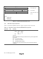
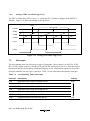
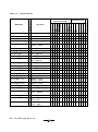
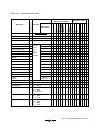
Table 1.1 lists the features of the H8/338 Series.
Rev. 3.0, 09/98, page 1 of 361
Table 1.1
Features
Item
Specification
CPU
Two-way general register configuration
•
Eight 16-bit registers, or
•
Sixteen 8-bit registers
High-speed operation
•
Maximum clock rate: 10MHz
•
Add/subtract:
0.2µs
•
Multiply/divide:
1.4µs
Streamlined, concise instruction set
•
Instruction length: 2 or 4 bytes
•
Register-register arithmetic and logic operations
•
MOV instruction for data transfer between registers and memory
Instruction set features
Memory
16-bit freerunning timer
(1 channel)
8-bit timer
(2 channels)
•
Multiply instruction (8 bits × 8 bits)
•
Divide instruction (16 bits ÷ 8 bits)
•
Bit-accumulator instructions
•
Register-indirect specification of bit positions
•
H8/338: 48k-byte ROM; 2k-byte RAM
•
H8/337: 32k-byte ROM; 1k-byte RAM
•
H8/336: 24k-byte ROM; 1k-byte RAM
•
One 16-bit free-running counter (can also count external events)
•
Two output-compare lines
•
Four input capture lines (can be buffered)
Each channel has
•
One 8-bit up-counter (can also count external events)
•
Two time constant registers
PWM timer
(2 channels)
•
Duty cycle can be set from 0 to 100%
•
Resolution: 1/250
Serial
communication
interface (SCI)
(2 channels)
•
Asynchronous or clocked synchronous mode (selectable)
•
Full duplex: can transmit and receive simultaneously
•
On-chip baud rate generator
Rev. 3.0, 09/98, page 2 of 361
Table 1.1
Features (cont)
Item
Specification
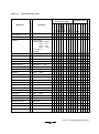
A/D converter
•
8-bit resolution
•
Eight channels: single or scan mode (selectable)
•
Start of A/D conversion can be externally triggered
•
Sample-and-hold function
•
8-bit resolution
•
Two channels
•
58 input/output lines (16 of which can drive LEDs)
•
8 input-only lines
•
Nine external interrupt lines: NMI, IRQ0 to IRQ7
•
22 on-chip interrupt sources
•
Expanded mode with on-chip ROM disabled (mode 1)
•
Expanded mode with on-chip ROM enabled (mode 2)
•
Single-chip mode (mode 3)
•
Sleep mode
•
Software standby mode
•
Hardware standby mode
•
On-chip oscillator
D/A converter
I/O ports
Interrupts
Operating
modes
Power-down
modes
Other features
Series lineup
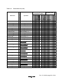
5-V version
3-V version
Package
ROM
HD6473388CG HD6473388VCG 84-pin windowed LCC (CG-84) PROM
HD6473388F
HD6473388VF
80-pin QFP (FP-80A)
HD6433388CP HD6433388VCP 84-pin PLCC (CP-84)
HD6433388F
HD6433388VF
80-pin QFP (FP-80A)
HD6413388F
HD6413388VF
80-pin QFP (FP-80A)
Masked ROM
ROMless
HD6473378CG HD6473378VCG 84-pin windowed LCC (CG-84) PROM
HD6473378F
HD6473378VF
80-pin QFP (FP-80A)
HD6433378CP HD6433378VCP 84-pin PLCC (CP-84)
HD6433378F
HD6433378VF
80-pin QFP (FP-80A)
HD6413378F
HD6413378VF
80-pin QFP (FP-80A)
HD6433368CP HD6433368VCP 84-pin PLCC (CP-84)
HD6433368F
HD6433368VF
Masked ROM
ROMless
Masked ROM
80-pin QFP (FP-80A)
Rev. 3.0, 09/98, page 3 of 361
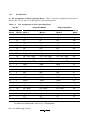
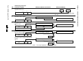
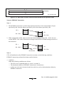
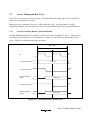
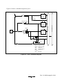
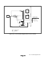
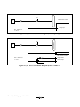
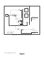
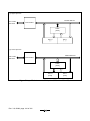
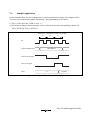
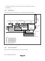
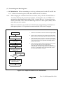
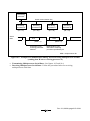
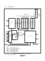
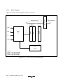
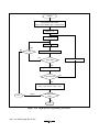
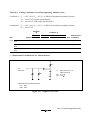
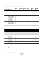
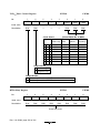
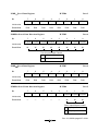
1.2
Block Diagram
*1
RES
STBY
NMI
MD1
MD0
VCC
VCC
VSS
VSS
VSS
VSS
VSS
VSS
VSS
Clock
pulse
generator
Port 9
Data (High)
Port 1
PROM *2
(or masked ROM)
P90/ADTRG /IRQ2
P91/IRQ1
P92/IRQ0
P93/RD
P94/WR
P95/AS
P96/Ø
P97/WAIT
Port 3
P20 /A8
P21 /A9
P2 2 /A10
P2 3 /A11
P2 4 /A12
P2 5 /A13
P2 6 /A14
P2 7 /A15
Data bus (Low)
Port 2
P10/A0
P11/A1
P12/A2
P13/A3
P14/A4
P15/A5
P16/A6
P17/A7
CPU
H8/300
Address bus
XTAL
EXTAL
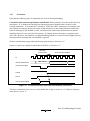
Figure 1.1 shows a block diagram of the H8/338 Series.
P30/D0
P31/D1
P32/D2
P33/D3
P34/D4
P35/D5
P36/D6
P37/D7
RAM
16 -bit freerunning timer
Serial
communication
(2 channels)
8-bit timer
(2 channels)
8-bit D/A converter
(8 channels)
P60/FTCI
P61/FTOA
8-bit D/A converter
(2 channels)
Port 8
PWM timer
(2 channels)
Port 6
P80
P81
P82
P83
P84/TxD1/IRQ3
P85/RxD1/IRQ4
P86/SCK1/IRQ5
Notes: 1. CP-84 and CG-84 only.
2. PROM is available in the H8/338 and H8/337 only.
P52 /SCK0
P50 /TxD0
Memory Sizes
H8/338
H8/337
H8/336
ROM
48k bytes
32k bytes
24k bytes
RAM
2k bytes
1k byte
1k byte
Figure 1.1 Block Diagram
Rev. 3.0, 09/98, page 4 of 361
P51 /RxD0
Port 5
P77/AN7/DA1
P76/AN6/DA0
P75/AN5
P74/AN4
P73/AN3
P72/AN2
P71/AN1
P70/AN0
Port 7
P40/TMCI0
P41/TMO0
P42/TMRI0
P43/TMCI1
P44/TMO1
P45/TMRI1
P46/PW0
P47/PW1
Port 4
AVCC
AVSS
P62 /FTIA
P63 /FTIB
P64/FTIC
P65 /FTID
P66/FTOB/IRQ6
P67 /IRQ7
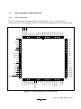
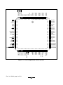
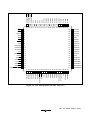
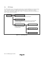
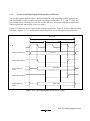
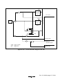
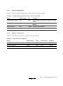
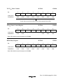
1.3
Pin Assignments and Functions
1.3.1
Pin Arrangement
5
4
3
2
1 84 83 82 81 80 79 78 77 76 75
P13 /A3
6
P12 /A2
7
P11 /A1
8
P10 /A0
P36 /D6
P30 /D0
VSS
P31 /D1
P37 /D7
P32 /D2
VSS
P33 /D3
P80
P34 /D4
P81
P35 /D5
P82
11 10 9
P83
P84 /TxD1/IRQ3
P85 /RxD1/IRQ4
P86 /SCK1/IRQ5
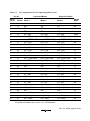
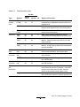
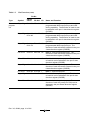
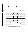
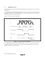
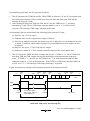
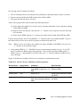
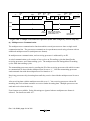
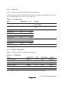
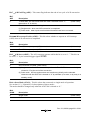
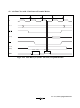
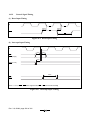
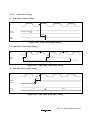
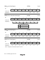
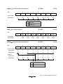
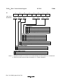
Figure 1.2 shows the pin arrangement of the CG-84 package. Figure 1.3 shows the pin
arrangement of the CP-84 package. Figure 1.4 shows the pin arrangement of the FP-80A package.
RES 12
74 P14 /A4
XTAL 13
73 P15 /A5
EXTAL 14
72 P16 /A6
MD1 15
71 P17 /A7
MD0 16
70 VSS
NMI 17
69 P20 /A8
STBY 18
68 P21 /A9
VCC 19
67 P22 /A10
P52 /SCK0 20
66 P23 /A11
P51 /RxD0 21
65 P24 /A12
P50 /TxD0 22
64 VSS
VSS 23
63 P25 /A13
VSS 24
62 P26 /A14
P97/WAIT 25
61 P27 /A15
60 VCC
P96 /Ø 26
P9 5 /AS 27
59 P47 /PW1
P9 4 /WR 28
58 P46 /PW0
P93 /RD 29
57 P45 /TMRI1
P92 /IRQ0 30
56 P44 /TMO1
P91 /IRQ1 31
55 P43 /TMCI1
P9 0 /IRQ2 /ADTRG 32
54 P42 /TMRI0
P41/TMO 0
P40/TMCI 0
AVSS
P77/AN7/DA1
P76/AN6/DA0
P75/AN5
P74/AN4
P73/AN3
P72/AN2
P71/AN1
P70/AN0
AVCC
VSS
P67 /IRQ7
P66 /FTOB/IRQ6
P65 /FTID
P64 /FTIC
P63 /FTIB
P6 2 /FTIA
P60 /FTCI
P61 /FTOA
33 34 35 36 37 38 39 40 41 42 43 44 45 46 47 48 49 50 51 52 53
Figure 1.2 Pin Arrangement (CG-84, Top view)
Rev. 3.0, 09/98, page 5 of 361
P86/SCK1/IRQ5
P85/RxD1/IRQ4
P84/TxD1/IRQ3
P83
P82
P81
P80
VSS
P37/D7
VSS
P36/D6
P35/D5
P34/D4
P33/D3
P32/D2
P31/D1
P30/D0
P10/A0
P11/A1
P12/A2
P13/A3
11 10 9 8 7 6 5 4 3 2 1 84 83 82 81 80 79 78 77 76 75
RES
XTAL
EXTAL
MD1
MD0
NMI
STBY
VCC
P52/SCK0
P51/RxD0
P50/TxD0
VSS
VSS
P97/WAIT
P96/Ø
P95/AS
P94/WR
P93/RD
P92/IRQ0
P91/IRQ1
P90/IRQ2/ADTRG
74
73
72
71
70
69
68
67
66
65
64
63
62
61
60
59
58
57
56
55
54
12
13
14
15
16
17
18
19
20
21
22
23
24
25
26
27
28
29
30
31
32
VSS
AVCC
P70/AN0
P71/AN1
P72/AN2
P73/AN3
P74/AN4
P75/AN5
P76/AN6/DA0
P77/AN7/DA1
AVSS
P40/TMCI0
P41/TMO0
P60 /FTCI
P61/FTOA
P62 /FTIA
P63 /FTIB
P64 /FTIC
P65 /FTID
P66/FTOB/IRQ6
P67/IRQ7
33 34 35 36 37 38 39 40 41 42 43 44 45 46 47 48 49 50 51 52 53
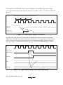
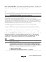
Figure 1.3 Pin Arrangement (CP-84, Top view)
Rev. 3.0, 09/98, page 6 of 361
P14/A4
P15/A5
P16/A6
P17/A7
VSS
P20/A8
P21/A9
P22/A10
P23/A11
P24/A12
VSS
P25 /A13
P26 /A14
P27 /A15
VCC
P47/PW1
P46/PW0
P45/TMRI1
P44/TMO1
P43/TMCI1
P42/TMRI0
P13/A3
P12/A2
P11/A1
P10/A0
P30/D0
P31/D1
P32/D2
P33/D3
P34/D4
P35/D5
P36/D6
P37/D7
VSS
P80
P81
P82
P83
P84/TxD1/IRQ3
P85/RxD1/IRQ4
P86/SCK1/IRQ5
80 79 78 77 76 75 74 73 72 71 70 69 68 67 66 65 64 63 62 61
RES
1
60
P14 /A4
XTAL
2
59
P15 /A5
EXTAL
3
58
P16 /A6
MD1
4
57
P17 /A7
MD0
5
56
VSS
NMI
6
55
P20/A8
STBY
7
54
P21/A9
VCC
8
53
P22/A10
P52/SCK0
9
52
P23/A11
P51/RxD0
10
51
P24/A12
P50/TxD0
11
50
P25/A13
VSS
12
49
P26/A14
P97/WAIT
13
48
P27/A15
P96/Ø
14
47
VCC
P95/AS
15
46
P47/PW1
P94/WR
16
45
P46/PW0
P93/RD
17
44
P45/TMRI1
P92/IRQ0
18
43
P44/TMO1
P91/IRQ1
19
42
P43/TMCI1
P90/ADTRG/IRQ2
20
41
P42/TMRI0
P41/TMO0
P40/TMCI0
AVSS
P77/AN7/DA1
P76/AN6/DA0
P75/AN5
P74/AN4
P73/AN3
P72/AN2
P71/AN1
P70/AN0
AVCC
P6 7/IRQ7
P66/FTOB/IRQ6
P65/FTID
P64/FTIC
P63/FTIB
P62/FTIA
P60/FTCI
P61/FTOA
21 22 23 24 25 26 27 28 29 30 31 32 33 34 35 36 37 38 39 40
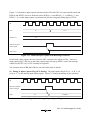
Figure 1.4 Pin Arrangement (FP-80A, Top view)
Rev. 3.0, 09/98, page 7 of 361
1.3.2
Pin Functions
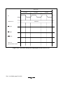
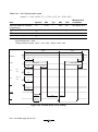
(1) Pin Assignments in Each Operating Mode: Table 1.2 lists the assignments of the pins of
the FP-80A, CP-84, and CG-84 packages in each operating mode.
Table 1.2
Pin Assignments in Each Operating Mode
Pin No.
Expanded Modes
Single-Chip Mode
CP-84
CG-84
FP-80A Mode 1
Mode 2
Mode 3
PROM
Mode
1
71
D6
D6
P36
EO6
2
VSS
VSS
VSS
VSS
3
72
D7
D7
P37
EO7
4
73
VSS
VSS
VSS
VSS
5
74
P80
P80
P80
NC
6
75
P81
P81
P81
NC
7
76
P82
P82
P82
NC
8
77
P83
P83
P83
NC
9
78
P84 / TxD1 / IRQ3
P84 / TxD1 / IRQ3
P84 / TxD1 / IRQ3
NC
10
79
P85 / RxD1 / IRQ4
P85 / RxD1 / IRQ4
P85 / RxD1 / IRQ4
NC
11
80
P86 / SCK1 / IRQ5
P86 / SCK1 / IRQ5
P86 / SCK1 / IRQ5
NC
12
1
RES
RES
RES
VPP
13
2
XTAL
XTAL
XTAL
NC
14
3
EXTAL
EXTAL
EXTAL
NC
15
4
MD1
MD1
MD1
VSS
16
5
MD0
MD0
MD0
VSS
17
6
NMI
NMI
NMI
EA9
18
7
STBY
STBY
STBY
VSS
19
8
VCC
VCC
VCC
VCC
20
9
P52 / SCK0
P52 / SCK0
P52 / SCK0
NC
21
10
P51 / RxD0
P51 / RxD0
P51 / RxD0
NC
22
11
P50 / TxD0
P50 / TxD0
P50 / TxD0
NC
23
12
VSS
VSS
VSS
VSS
24
VSS
VSS
VSS
VSS
25
13
WAIT
WAIT
P97
NC
Note: Pins marked NC should be left unconnected.
For details on PROM mode, refer to 14.2, “PROM Mode.”
Rev. 3.0, 09/98, page 8 of 361
Table 1.2
Pin Assignments in Each Operating Mode (cont)
Pin No.
Expanded Modes
CP-84
CG-84
FP-80A Mode 1
26
14
27
Single-Chip Mode
Mode 2
Mode 3
PROM
Mode
φ
φ
P96 / φ
NC
15
AS
AS
P95
NC
28
16
WR
WR
P94
NC
29
17
RD
RD
P93
NC
30
18
P92 / IRQ0
P92 / IRQ0
P92 / IRQ0
PGM
31
19
P91 / IRQ1
P91 / IRQ1
P91 / IRQ1
EA15
32
20
P90 / ADTRG / IRQ2
P90 / ADTRG / IRQ2
P90 / ADTRG / IRQ2
EA16
33
21
P60 / FTCI
P60 / FTCI
P60 / FTCI
NC
34
22
P61 / FTOA
P61 / FTOA
P61 / FTOA
NC
35
23
P62 / FTIA
P62 / FTIA
P62 / FTIA
NC
36
24
P63 / FTIB
P63 / FTIB
P63 / FTIB
VCC
37
25
P64 / FTIC
P64 / FTIC
P64 / FTIC
VCC
38
26
P65 / FTID
P65 / FTID
P65 / FTID
NC
39
27
P66 / FTOB / IRQ6
P66 / FTOB / IRQ6
P66 / FTOB / IRQ6
NC
40
28
P67 / IRQ7
P67 / IRQ7
P67 / IRQ7
NC
41
VSS
VSS
VSS
VSS
42
29
AVCC
AVCC
AVCC
VCC
43
30
P70 / AN0
P70 / AN0
P70 / AN0
NC
44
31
P71 / AN1
P71 / AN1
P71 / AN1
NC
45
32
P72 / AN2
P72 / AN2
P72 / AN2
NC
46
33
P73 / AN3
P73 / AN3
P73 / AN3
NC
47
34
P74 / AN4
P74 / AN4
P74 / AN4
NC
48
35
P75 / AN5
P75 / AN5
P75 / AN5
NC
49
36
P76 / AN6 /DA0
P76 / AN6 /DA0
P76 / AN6 /DA0
NC
50
37
P77 / AN7 /DA1
P77 / AN7 /DA1
P77 / AN7 /DA1
NC
51
38
AVSS
AVSS
AVSS
VSS
52
39
P40 / TMCI0
P40 / TMCI0
P40 / TMCI0
NC
53
40
P41 / TMO0
P41 / TMO0
P41 / TMO0
NC
54
41
P42 / TMRI0
P42 / TMRI0
P42 / TMRI0
NC
Note: Pins marked NC should be left unconnected.
For details on PROM mode, refer to 14.2, “PROM Mode.”
Rev. 3.0, 09/98, page 9 of 361
Table 1.2
Pin Assignments in Each Operating Mode (cont)
Pin No.
Expanded Modes
Single-Chip Mode
CP-84
CG-84
FP-80A Mode 1
Mode 2
Mode 3
PROM
Mode
55
42
P43 / TMCI1
P43 / TMCI1
P43 / TMCI1
NC
56
43
P44 / TMO1
P44 / TMO1
P44 / TMO1
NC
57
44
P45 / TMRI1
P45 / TMRI1
P45 / TMRI1
NC
58
45
P46 / PW0
P46 / PW0
P46 / PW0
NC
59
46
P47 / PW1
P47 / PW1
P47 / PW1
NC
60
47
VCC
VCC
VCC
VCC
61
48
A15
P27 / A15
P27
CE
62
49
A14
P26 / A14
P26
EA14
63
50
A13
P25 / A13
P25
EA13
64
VSS
VSS
VSS
VSS
65
51
A12
P24 / A12
P24
EA12
66
52
A11
P23 / A11
P23
EA11
67
53
A10
P22 / A10
P22
EA10
68
54
A9
P21 / A9
P21
OE
69
55
A8
P20 / A8
P20
EA8
70
56
VSS
VSS
VSS
VSS
71
57
A7
P17 / A7
P17
EA7
72
58
A6
P16 / A6
P16
EA6
73
59
A5
P15 / A5
P15
EA5
74
60
A4
P14 / A4
P14
EA4
75
61
A3
P13 / A3
P13
EA3
76
62
A2
P12 / A2
P12
EA2
77
63
A1
P11 / A1
P11
EA1
78
64
A0
P10 / A0
P10
EA0
79
65
D0
D0
P30
EO0
80
66
D1
D1
P31
EO1
81
67
D2
D2
P32
EO2
82
68
D3
D3
P33
EO3
83
69
D4
D4
P34
EO4
84
70
D5
D5
P35
EO5
Note: Pins marked NC should be left unconnected.
For details on PROM mode, refer to 14.2, “PROM Mode.”
Rev. 3.0, 09/98, page 10 of 361
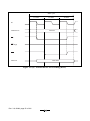
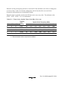
(2) Pin Functions: Table 1.3 gives a concise description of the function of each pin.
Table 1.3
Pin Functions
Pin No.
Type
Symbol
CG-84
CP-84
FP-80A I/O
Name and Function
Power
VCC
19, 60
8, 47
I
Power: Connected to the power supply (+5V).
Connect both VCC pins to the system power
supply (+5V).
VSS
2, 4, 23, 12, 56,
24, 41, 73
64, 70
I
Ground: Connected to ground (0V). Connect
all VSS pins to the system power supply (0V).
XTAL
13
2
I
Crystal: Connected to a crystal oscillator. The
crystal frequency should be double the desired
system clock frequency
EXTAL
14
3
I
External crystal: Connected to a crystal
oscillator or external clock. The frequency of
the external clock should be double the desired
system clock frequency. See section 15.2,
“Oscillator Circuit,” for examples of connections
to a crystal and external clock.
∅
26
14
O
System clock: Supplies the system clock to
peripheral devices.
RES
12
1
I
Reset: A Low input causes the chip to reset.
STBY
18
7
I
Standby: A transition to the hardware standby
mode (a power-down state) occurs when a Low
input is received at the STBY pin.
Address
bus
A15 to A0
61 to 63, 48 to 55, O
65 to 69, 57 to 64
71 to 78
Address bus: Address output pins.
Data bus
D7 to D0
3, 1,
72 to 65 I/O
84 to 79
Data bus: 8-Bit bidirectional data bus.
Clock
System
control
Rev. 3.0, 09/98, page 11 of 361
Table 1.3
Pin Functions (cont)
Pin No.
Type
CG-84
CP-84
FP-80A I/O
Name and Function
25
13
I
Wait: Requests the CPU to insert TW states
into the bus cycle when an external address is
accessed.
RD
29
17
O
Read: Goes Low to indicate that the CPU is
reading an external address.
WR
28
16
O
Write: Goes Low to indicate that the CPU is
writing to an external address.
AS
27
15
O
Address Strobe: Goes Low to indicate that
there is a valid address on the address bus.
NMI
17
6
I
NonMaskable Interrupt: Highest-priority
interrupt request. The NMIEG bit in the system
control register determines whether the
interrupt is requested on the rising or falling
edge of the NMI input.
IRQ0 to
IRQ7
30 to 32, 18 to 20, I
9 to 11, 78 to 80,
39, 40
27, 28
Interrupt Request 0 to 7: Maskable interrupt
request pins.
MD1,
MD0
15
16
Mode: Input pins for setting the MCU
operating mode according to the table below.
Symbol
Bus control WAIT
Interrupt
signals
Operating
mode
control
4
5
I
MD1
MD0
Mode
Description
0
0
Mode 0 Setting prohibited
0
1
Mode 1 Expanded mode with
on-chip ROM disabled
1
0
Mode 2 Expanded mode with
on-chip ROM enabled
1
1
Mode 3 Single-chip mode
These pins must not be changed during MCU
operation.
Serial
communication
interface
TxD0,
TxD1
22
9
11
78
O
Transmit Data (channels 0 and 1): Data
output pins for the serial communication
interface.
RxD0,
RxD1
21
10
10
79
I
Receive Data (channels 0 and 1): Data input
pins for the serial communication interface.
SCK0,
SCK1
20
11
9
80
I/O
Serial Clock (channels 0 and 1): Input/output
pins for the serial clock.
Rev. 3.0, 09/98, page 12 of 361
Table 1.3
Pin Functions (cont)
Pin No.
CG-84
CP-84
FP-80A I/O
Name and Function
34
39
22
27
O
FRT Output compare A and B: Output pins
controlled by comparators A and B of the freerunning timer.
FTCI
33
21
I
FRT counter Clock Input: Input pin for an
external clock signal for the free-running timer.
FTIA to
FTID
35 to 38 23 to 26 I
FRT Input capture A to D: Input capture pins
for the free-running timer.
TMO0,
TMO1
53
56
40
43
O
8-bit Timer Output (channels 0 and 1):
Compare-match output pins for the 8-bit timers.
TMCI0,
TMCI1
52
55
39
42
I
8-bit Timer counter Clock Input (channels 0
and 1): External clock input pins for the 8-bit
timer counters.
TMRI0,
TMRI1
54
57
41
44
I
8-bit Timer counter Reset Input (channels 0
and 1): A High input at these pins resets the 8bit timer counters.
PWM
timer
PW0,
PW1
58
59
45
46
O
PWM timer output (channels 0 and 1):
Pulse-width modulation timer output pins.
A/D
converter
AN7 to
AN0
50 to 43 37 to 30 I
Analog input: Analog signal input pins for the
A/D converter.
ADTRG
32
20
I
A/D Trigger: External trigger input for starting
the A/D converter.
DA0
DA1
49
50
36
37
O
Analog output: Analog signal output pins for
the D/A converter.
A/D and
AVCC
D/A
converters
42
29
I
Analog reference Voltage: Reference voltage
pin for the A/D and D/A converters. If the A/D
and D/A converters are not used, connect
AVCC to the system power supply (+5V).
AVSS
51
38
I
Analog ground: Ground pin for the A/D and
D/A converters.Connect to system ground (0V).
Type
Symbol
16-bit free- FTOA,
running
FTOB
timer
8-bit timer
D/A
converter
Rev. 3.0, 09/98, page 13 of 361
Table 1.3
Pin Functions (cont)
Pin No.
Type
Symbol
CG-84
CP-84
Generalpurpose
I/O
P17 to P10
71 to 78 57 to 64 I/O
Port 1: An 8-bit input/output port with
programmable MOS input pull-ups and LED
driving capability. The direction of each bit can
be selected in the port 1 data direction register
(P1DDR).
P27 to P20
61 to 63, 48 to 55 I/O
65 to 69
Port 2: An 8-bit input/output port with
programmable MOS input pull-ups and LED
driving capability. The direction of each bit can
be selected in the port 2 data direction register
(P2DDR).
P37 to P30
3, 1,
72 to 65 I/O
84 to 79
Port 3: An 8-bit input/output port with
programmable MOS input pull-ups. The
direction of each bit can be selected in the port
3 data direction register (P3DDR).
P47 to P40
59 to 52 46 to 39 I/O
Port 4: An 8-bit input/output port. The
direction of each bit can be selected in the port
4 data direction register (P4DDR).
P52 to P50
20 to 22 9 to 11
I/O
Port 5: A 3-bit input/output port. The direction
of each bit can be selected in the port 5 data
direction register (P5DDR).
P67 to P60
40 to 33 28 to 21 I/O
Port 6: An 8-bit input/output port. The
direction of each bit can be selected in the port
6 data direction register (P6DDR).
P77 to P70
50 to 43 37 to 30 I
Port 7: An 8-bit input port.
P86 to P80
11 to 5
Port 8: A 7-bit input/output port. The direction
of each bit can be selected in the port 8 data
direction register (P8DDR).
P97 to P90
25 to 32 13 to 20 I/O
Rev. 3.0, 09/98, page 14 of 361
FP-80A I/O
80 to 74 I/O
Name and Function
Port 9: An 8-bit input/output port. The
direction of each bit (except for P96) can be
selected in the port 9 data direction register
(P9DDR).
Section 2 CPU
2.1
Overview
The H8/338 Series has the H8/300 CPU: a fast central processing unit with eight 16-bit general
registers (also configurable as 16 eight-bit registers) and a concise instruction set designed for
high-speed operation.
2.1.1
Features
The main features of the H8/300 CPU are listed below.
• Two-way register configuration
Sixteen 8-bit general registers, or
Eight 16-bit general registers
• Instruction set with 57 basic instructions, including:
Multiply and divide instructions
Powerful bit-manipulation instructions
• Eight addressing modes
Register direct (Rn)
Register indirect (@Rn)
Register indirect with displacement (@(d:16, Rn))
Register indirect with post-increment or pre-decrement (@Rn+ or @−Rn)
Absolute address (@aa:8 or @aa:16)
Immediate (#xx:8 or #xx:16)
PC-relative (@(d:8, PC))
Memory indirect (@@aa:8)
• Maximum 64K-byte address space
• High-speed operation
All frequently-used instructions are executed in two to four states
The maximum clock rate is 10MHz
8- or 16-bit register-register add or subtract: 0.2µs
1.4µs
8 × 8-bit multiply:
16 ÷ 8-bit divide:
• Power-down mode
SLEEP instruction
1.4µs
Rev. 3.0, 09/98, page 15 of 361
2.2
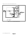
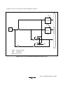
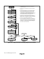
Register Configuration
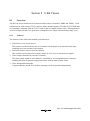
Figure 2.1 shows the register structure of the CPU. There are two groups of registers: the general
registers and control registers.
7
07
0
R0H
R0L
R1H
R1L
R2H
R2L
R3H
R3L
R4H
R4L
R5H
R5L
R6H
R6L
R7H
(SP)
15
R7L
SP: Stack Pointer
0
PC: Program Counter
PC
7 6 5 4 3 2 1 0
CCR I U H U N Z V C
CCR: Condition Code Register
Carry flag
Overflow flag
Zero flag
Negative flag
Half-carry flag
Interrupt mask bit
User bit
User bit
Figure 2.1 CPU Registers
Rev. 3.0, 09/98, page 16 of 361
2.2.1
General Registers
All the general registers can be used as both data registers and address registers. When used as
address registers, the general registers are accessed as 16-bit registers (R0 to R7). When used as
data registers, they can be accessed as 16-bit registers, or the high and low bytes can be accessed
separately as 8-bit registers (R0H to R7H and R0L to R7L).
R7 also functions as the stack pointer, used implicitly by hardware in processing interrupts and
subroutine calls. In assembly-language coding, R7 can also be denoted by the letters SP. As
indicated in figure 2.2, R7 (SP) points to the top of the stack.
Unused area
SP
(R7)
Stack area
Figure 2.2 Stack Pointer
2.2.2
Control Registers
The CPU control registers include a 16-bit program counter (PC) and an 8-bit condition code
register (CCR).
(1) Program Counter (PC): This 16-bit register indicates the address of the next instruction the
CPU will execute. Each instruction is accessed in 16 bits (1 word), so the least significant bit of
the PC is ignored (always regarded as 0).
(2) Condition Code Register (CCR): This 8-bit register contains internal status information,
including carry (C), overflow (V), zero (Z), negative (N), and half-carry (H) flags and the interrupt
mask bit (I).
Bit 7Interrupt Mask Bit (I): When this bit is set to “1,” all interrupts except NMI are masked.
This bit is set to “1” automatically by a reset and at the start of interrupt handling.
Bit 6User Bit (U): This bit can be written and read by software (using the LDC, STC, ANDC,
ORC, and XORC instructions).
Bit 5Half-Carry Flag (H): This flag is set to “1” when the ADD.B, ADDX.B, SUB.B,
SUBX.B, NEG.B, or CMP.B instruction causes a carry or borrow out of bit 3, and is cleared to
Rev. 3.0, 09/98, page 17 of 361
“0” otherwise. Similarly, it is set to “1” when the ADD.W, SUB.W, or CMP.W instruction causes
a carry or borrow out of bit 11, and cleared to “0” otherwise. It is used implicitly in the DAA and
DAS instructions.
Bit 4User Bit (U): This bit can be written and read by software (using the LDC, STC, ANDC,
ORC, and XORC instructions).
Bit 3Negative Flag (N): This flag indicates the most significant bit (sign bit) of the result of an
instruction.
Bit 2Zero Flag (Z): This flag is set to “1” to indicate a zero result and cleared to “0” to
indicate a nonzero result.
Bit 1Overflow Flag (V): This flag is set to “1” when an arithmetic overflow occurs, and
cleared to “0” at other times.
Bit 0Carry Flag (C): This flag is used by:
• Add and subtract instructions, to indicate a carry or borrow at the most significant bit of the
result
• Shift and rotate instructions, to store the value shifted out of the most significant or least
significant bit
• Bit manipulation and bit load instructions, as a bit accumulator
The LDC, STC, ANDC, ORC, and XORC instructions enable the CPU to load and store the CCR,
and to set or clear selected bits by logic operations. The N, Z, V, and C flags are used in
conditional branching instructions (BCC).
For the action of each instruction on the flag bits, see the H8/300 Series Programming Manual.
2.2.3
Initial Register Values
When the CPU is reset, the program counter (PC) is loaded from the vector table and the interrupt
mask bit (I) in the CCR is set to “1.” The other CCR bits and the general registers are not
initialized.
In particular, the stack pointer (R7) is not initialized. To prevent program crashes the stack pointer
should be initialized by software, by the first instruction executed after a reset.
Rev. 3.0, 09/98, page 18 of 361
2.3
Addressing Modes
2.3.1
Addressing Mode
The H8/300 CPU supports eight addressing modes. Each instruction uses a subset of these
addressing modes.
Table 2.1
Addressing Modes
No.
Addressing mode
Symbol
(1)
Register direct
Rn
(2)
Register indirect
@Rn
(3)
Register indirect with displacement
@(d:16, Rn)
(4)
Register indirect with post-increment
Register indirect with pre-decrement
@Rn+
@−Rn
(5)
Absolute address
@aa:8 or @aa:16
(6)
Immediate
#xx:8 or #xx:16
(7)
Program-counter-relative
@(d:8, PC)
(8)
Memory indirect
@@aa:8
(1) Register DirectRn: The register field of the instruction specifies an 8- or 16-bit general
register containing the operand. In most cases the general register is accessed as an 8-bit register.
Only the MOV.W, ADD.W, SUB.W, CMP.W, ADDS, SUBS, MULXU (8 bits × 8 bits), and
DIVXU (16 bits ÷ 8 bits) instructions have 16-bit operands.
(2) Register indirect@Rn: The register field of the instruction specifies a 16-bit general
register containing the address of the operand.
(3) Register Indirect with Displacement@(d:16, Rn): This mode, which is used only in
MOV instructions, is similar to register indirect but the instruction has a second word (bytes 3 and
4) which is added to the contents of the specified general register to obtain the operand address.
For the MOV.W instruction, the resulting address must be even.
(4) Register Indirect with Post-Increment or Pre-Decrement@Rn+ or @−Rn:
• Register indirect with Post-Increment@Rn+
The @Rn+ mode is used with MOV instructions that load registers from memory.
It is similar to the register indirect mode, but the 16-bit general register specified in the register
field of the instruction is incremented after the operand is accessed. The size of the increment
is 1 or 2 depending on the size of the operand: 1 for MOV.B; 2 for MOV.W. For MOV.W,
the original contents of the 16-bit general register must be even.
Rev. 3.0, 09/98, page 19 of 361
• Register Indirect with Pre-Decrement@−Rn
The @−Rn mode is used with MOV instructions that store register contents to memory.
It is similar to the register indirect mode, but the 16-bit general register specified in the register
field of the instruction is decremented before the operand is accessed. The size of the
decrement is 1 or 2 depending on the size of the operand: 1 for MOV.B; 2 for MOV.W. For
MOV.W, the original contents of the 16-bit general register must be even.
(5) Absolute Address@aa:8 or @aa:16: The instruction specifies the absolute address of the
operand in memory. The MOV.B instruction uses an 8-bit absolute address of the form H'FFxx.
The upper 8 bits are assumed to be 1, so the possible address range is H'FF00 to H'FFFF (65280 to
65535). The MOV.B, MOV.W, JMP, and JSR instructions can use 16-bit absolute addresses.
(6) Immediate#xx:8 or #xx:16: The instruction contains an 8-bit operand in its second byte,
or a 16-bit operand in its third and fourth bytes. Only MOV.W instructions can contain 16-bit
immediate values.
The ADDS and SUBS instructions implicitly contain the value 1 or 2 as immediate data. Some bit
manipulation instructions contain 3-bit immediate data (#xx:3) in the second or fourth byte of the
instruction, specifying a bit number.
(7) Program-Counter-Relative@(d:8, PC): This mode is used to generate branch addresses
in the BCC and BSR instructions. An 8-bit value in byte 2 of the instruction code is added as a
sign-extended value to the program counter contents. The result must be an even number. The
possible branching range is −126 to +128 bytes (−63 to +64 words) from the current address.
(8) Memory Indirect@@aa:8: This mode can be used by the JMP and JSR instructions. The
second byte of the instruction code specifies an 8-bit absolute address from H'0000 to H'00FF (0
to 255). The word located at this address contains the branch address. The upper 8 bits of the
absolute address are an “0” (H'00), thus the branch address is limited to values from 0 to 255
(H'0000 to H'00FF). Note that addresses H'0000 to H'0047 (0 to 71) are located in the vector
table.
If an odd address is specified as a branch destination or as the operand address of a MOV.W
instruction, the least significant bit is regarded as “0,” causing word access to be performed at the
address preceding the specified address. See section 2.4.2, “Memory Data Formats,” for further
information.
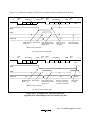
Rev. 3.0, 09/98, page 20 of 361
2.3.2
How to Calculate Where the Execution Starts
Table 2.2 shows how to calculate the Effective Address (EA: Effective Address) for each
addressing mode.
In the operation instruction, 1) register direct, as well as 6) immediate (for each instruction,
ADD.B, ADDX, SUBX, CMP.B, AND, OR, XOR) are used.
In the move instruction, 7) program counter relative and 8) all addressing mode to delete the
memory indirect can be used.
In the bit manipulation instruction for the operand specifications, 1) register direct, 2) register
indirect, as well as 5) absolute address (8 bit) can be used. Furthermore, to specify the bit number
within the operand, 1) register direct (for each instruction, BSET, BCLR, BNOT, BTST) as well
as 6) immediate (3 bit) can be used independently.
Rev. 3.0, 09/98, page 21 of 361
Addressing mode and
instruction format
1
Register direct, Rn
Effective address calculation
Effective address
3
0
regm
8 7
op
2
4 3
regm
Operands are contained in registers regm
and regn
15
0
16-bit register contents
7 6
op
3
4 3
15
0
15
0
15
0
15
0
0
reg
Register indirect with displacement,
@(d:16, Rn)
15
0
regn
0
regn
Register indirect, @Rn
15
3
7 6
op
4 3
15
0
16-bit register contents
0
reg
disp
disp
4
15
Register indirect with
post-increment, @Rn+
15
7 6
op
0
16-bit register contents
4 3
0
reg
1 or 2 *
Register indirect with pre-decrement,
@–Rn
15
7 6
op
4 3
15
0
16-bit register contents
0
reg
1 or 2 *
Note: * 1 for a byte operand, 2 for a word operand
Effective Address Calculation
15
Table 2.2
Rev. 3.0, 09/98, page 22 of 361
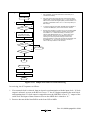
No.
5
Addressing mode and
instruction format
Effective address calculation
Effective address
15
Absolute address
@aa:8
8 7
op
0
0
abs
@aa:16
15
15
0
0
op
abs
6
Immediate
#xx:8
15
8 7
op
0
IMM
Operand is 1- or 2-byte immediate data
#xx:16
15
0
op
IMM
Rev. 3.0, 09/98, page 23 of 361
7
15
PC-relative
@(d:8, PC)
15
8 7
op
0
PC contents
0
disp
Sign extension
15
disp
0
Effective Address Calculation (cont)
15
8 7
H'FF
Table 2.2
No.
Table 2.2
No.
Addressing mode and
instruction format
8
Memory indirect, @@aa:8
15
Effective address calculation
8 7
op
Effective address
0
abs
15
8 7
0
H'00
15
Memory contents (16 bits)
Notation
reg: General register
op: Operation code
disp: Displacement
IMM: Immediate data
abs: Absolute address
0
Effective Address Calculation (cont)
Rev. 3.0, 09/98, page 24 of 361
Table 3-2. Effective Address Calculation (3)
2.4
Data Formats
The H8/300 CPU can process 1-bit data, 4-bit (BCD) data, 8-bit (byte) data, and 16-bit (word)
data.
• Bit manipulation instructions operate on 1-bit data specified as bit n (n = 0, 1, 2, ..., 7) in a byte
operand.
• All arithmetic and logic instructions except ADDS and SUBS can operate on byte data.
• The DAA and DAS instruction perform decimal arithmetic adjustments on byte data in packed
BCD form. Each nibble of the byte is treated as a decimal digit.
• The MOV.W, ADD.W, SUB.W, CMP.W, ADDS, SUBS, MULXU (8 bits × 8 bits), and
DIVXU (16 bits ÷ 8 bits) instructions operate on word data.
Rev. 3.0, 09/98, page 25 of 361
2.4.1
Data Formats in General Registers
Data of all the sizes above can be stored in general registers as shown in figure 2.3.
Data type
Register No.
Data format
7
1-Bit data
RnH
0
7
6
5
4
3
2
1
0
don't care
7
1-Bit data
RnL
don't care
Byte data
RnH MSB
Byte data
RnL
Word data
Rn
4-Bit BCD data
RnH
4-Bit BCD data
RnL
7
7
0
6
5
3
2
1
0
0
LSB
don't care
don't care
7
0
MSB
LSB
15
0
MSB
LSB
7
4
3
Upper digit
0
Lower digit
don't care
7
don't care
4
Upper digit
Legend
RnH
RnL
MSB
LSB
4
Upper digit of general register
Lower digit of general register
Most significant bit
Least significant bit it
Figure 2.3 Register Data Formats
Rev. 3.0, 09/98, page 26 of 361
3
0
Lower digit
2.4.2
Memory Data Formats
Figure 2.4 indicates the data formats in memory.
Word data stored in memory must always begin at an even address. In word access the least
significant bit of the address is regarded as “0.” If an odd address is specified, no address error
occurs but the access is performed at the preceding even address. This rule affects MOV.W
instructions and branching instructions, and implies that only even addresses should be stored in
the vector table.
Data type
Address
Data format
7
1-Bit data
Address n
7
Byte data
Address n MSB
Even address MSB
0
6
5
4
3
2
1
0
LSB
Upper 8 bits
Word data
Lower 8 bits
LSB
Even address MSB
CCR
LSB
Odd address MSB
CCR*
LSB
Odd address
Byte data (CCR) on stack
Even address MSB
Word data on stack
Odd address
LSB
Note: * Ignored when returned
Legend
CCR: Condition Code Register
Figure 2.4 Memory Data Formats
When the stack is addressed by register R7, it must always be accessed a word at a time. When
the CCR is pushed on the stack, two identical copies of the CCR are pushed to make a complete
word. When they are returned, the lower byte is ignored.
Rev. 3.0, 09/98, page 27 of 361
2.5
Instruction Set
Table 2.3 lists the H8/300 instruction set.
Table 2.3
Instruction Classification
Function
Instructions
Types
3
3
1
1
Data transfer
MOV, MOVTPE* , MOVFPE* , PUSH* , POP*
Arithmetic operations
ADD, SUB, ADDX, SUBX, INC, DEC, ADDS, SUBS,
DAA, DAS, MULXU, DIVXU, CMP, NEG
Logic operations
AND, OR, XOR, NOT
4
Shift
SHAL, SHAR, SHLL, SHLR, ROTL, ROTR, ROTXL,
ROTXR
8
Bit manipulation
BSET, BCLR, BNOT, BTST, BAND, BIAND, BOR, BIOR, 14
BXOR, BIXOR, BLD, BILD, BST, BIST
Branch
Bcc* , JMP, BSR, JSR, RTS
5
System control
RTE, SLEEP, LDC, STC, ANDC, ORC, XORC, NOP
8
Block data transfer
EEPMOV
1
3
2
14
Total 57
Notes: 1. PUSH Rn is equivalent to MOV.W Rn, @−SP.
POP Rn is equivalent to MOV.W @SP+, Rn.
2. BCC is a conditional branch instruction in which cc represents a condition code.
3. Not supported by the H8/338 Series.
The following sections give a concise summary of the instructions in each category, and indicate
the bit patterns of their object code. The notation used is defined next.
Rev. 3.0, 09/98, page 28 of 361
Operation Notation
Rd
General register (destination)
Rs
General register (source)
Rn
General register
(EAd)
Destination operand
(EAs)
Source operand
SP
Stack pointer
PC
Program counter
CCR
Condition code register
N
N (negative) flag of CCR
Z
Z (zero) flag of CCR
V
V (overflow) flag of CCR
C
C (carry) flag of CCR
#imm
Immediate data
#xx:3
3-Bit immediate data
#xx:8
8-Bit immediate data
#xx:16
16-Bit immediate data
disp
Displacement
+
Addition
−
Subtraction
×
Multiplication
÷
Division
∧
AND logical
∨
OR logical
⊕
Exclusive OR logical
→
Move
¬
Not
Rev. 3.0, 09/98, page 29 of 361
2.5.1
Data Transfer Instructions
Table 2.4 describes the data transfer instructions. Figure 2.5 shows their object code formats.
Table 2.4
Data Transfer Instructions
Instruction
Size*
Function
MOV
B/W
(EAs) → Rd, Rs → (EAd)
Moves data between two general registers or between a general register
and memory, or moves immediate data to a general register.
The Rn, @Rn, @(d:16, Rn), @aa:16, #xx:8 or #xx:16, @−Rn, and @Rn+
addressing modes are available for byte or word data. The @aa:8
addressing mode is available for byte data only.
The @−R7 and @R7+ modes require word operands. Do not specify
byte size for these two modes.
MOVTPE
B
Not supported by the H8/338 Series.
MOVFPE
B
Not supported by the H8/338 Series.
PUSH
W
Rn → @−SP
Pushes a 16-bit general register onto the stack. Equivalent to MOV.W
Rn, @−SP.
POP
W
@SP+ → Rn
Pops a 16-bit general register from the stack. Equivalent to MOV.W
@SP+, Rn.
Note: Size: operand size
B: Byte
W: Word
Rev. 3.0, 09/98, page 30 of 361
15
8
7
Op
0
rm
MOV
rn
Rm
Rn
@Rm, or @Rm
Op
rm
rn
Rn
Op
rm
rn
@(d:16, Rm)
Rn
disp.
Op
Op
rm
rn
rn
abs.
Op
rn
Op
rn
#imm.
@(d:16, Rm)
Rn, or Rn
@-Rm
@aa:8
Rn, or Rn
@aa:8
@aa:16
Rn. or
@aa:16
#XX:8
Op
rn
Rn,or
@Rm+
Rn
abs.
Rn
#XX:16
Rn
Rn
#imm.
Op
rn
MOVFRE, MOVTPE
rn
PUSH, POP
abs.
Op
Legend
Op
: Operation field
rm, rn : Register field
disp. : Displacement
abs.
: Absolute address
IMM : immediate data
Figure 2.5 Data Transfer Instruction Codes
Rev. 3.0, 09/98, page 31 of 361
2.5.2
Arithmetic Operations
Table 2.5 describes the arithmetic instructions. See figure 2.6 in section 2.5.4, “Shift Operations”
for their object codes.
Table 2.5
Arithmetic Instructions
Instruction
Size*
Function
ADD
SUB
B/W
Rd ± Rs → Rd, Rd + #imm → Rd
Performs addition or subtraction on data in two general registers, or
addition on immediate data and data in a general register. Immediate
data cannot be subtracted from data in a general register. Word data can
be added or subtracted only when both words are in general registers.
ADDX
SUBX
B
Rd ± Rs ± C → Rd, Rd ± #imm ± C → Rd
Performs addition or subtraction with carry or borrow on byte data in two
general registers, or addition or subtraction on immediate data and data in
a general register.
INC
DEC
B
Rd ± #1 → Rd
Increments or decrements a general register.
ADDS
SUBS
W
Rd ± #imm → Rd
Adds or subtracts immediate data to or from data in a general register.
The immediate data must be 1 or 2.
DAA
DAS
B
Rd decimal adjust → Rd
Decimal-adjusts (adjusts to packed BCD) an addition or subtraction result
in a general register by referring to the CCR.
MULXU
B
Rd × Rs → Rd
Performs 8-bit × 8-bit unsigned multiplication on data in two general
registers, providing a 16-bit result.
DIVXU
B
Rd ÷ Rs → Rd
Performs 16-bit ÷ 8-bit unsigned division on data in two general registers,
providing an 8-bit quotient and 8-bit remainder.
CMP
B/W
Rd − Rs, Rd − #imm
Compares data in a general register with data in another general register
or with immediate data. Word data can be compared only between two
general registers.
NEG
B
0 − Rd → Rd
Obtains the two’s complement (arithmetic complement) of data in a
general register.
Note: Size: operand size
B: Byte
W: Word
Rev. 3.0, 09/98, page 32 of 361
2.5.3
Logic Operations
Table 2.6 describes the four instructions that perform logic operations. See figure 2.6 in section
2.5.4, “Shift Operations,” for their object codes.
Table 2.6
Logic Operation Instructions
Instruction
Size*
Function
AND
B
Rd ∧ Rs → Rd,
Rd ∧ #imm → Rd
Performs a logical AND operation on a general register and another
general register or immediate data.
OR
B
Rd ∨ Rs → Rd,
Rd ∨ #imm → Rd
Performs a logical OR operation on a general register and another
general register or immediate data.
XOR
B
Rd ⊕ Rs → Rd,
Rd ⊕ #imm → Rd
Performs a logical exclusive OR operation on a general register and
another general register or immediate data.
NOT
B
¬ (Rd) → (Rd)
Obtains the one’s complement (logical complement) of general register
contents.
Note: Size: operand size
B: Byte
2.5.4
Shift Operations
Table 2.7 describes the eight shift instructions. Figure 2.6 shows the object code formats of the
arithmetic, logic, and shift instructions.
Table 2.7
Shift Instructions
Instruction
Size*
Function
SHAL
SHAR
B
Rd shift → Rd
Performs an arithmetic shift operation on general register contents.
SHLL
SHLR
B
Rd shift → Rd
Performs a logical shift operation on general register contents.
ROTL
ROTR
B
Rd rotate → Rd
Rotates general register contents.
ROTXL
ROTXR
B
Rd rotate through carry → Rd
Rotates general register contents through the C (carry) bit.
Note: Size: operand size
B: Byte
Rev. 3.0, 09/98, page 33 of 361
15
8
Op
7
0
rn
rm
ADD, AUB, CMP
ADDX, SUBX(Rm), MULXU, DIVXU
Op
rn
ADDS, SUBS, INC, DEC, DAA,
DAS, NEG, NOT
Op
#imm.
rn
ADD, ADDX, SUBX, CMP
(#XX:8)
Op
rm
Op
rn
Op
rn
#imm.
AND, OR, XOR(Rm)
AND, OR, XOR(#XX:8)
rn
SHAL, SHAR, SHLL, SHLR,
ROTL, ROTR, ROTXL, ROTXR
Legend:
Op
: Operation field
rm, rn : Register field
IMM : immediate data
Figure 2.6 Arithmetic, Logic, and Shift Instruction Codes
Rev. 3.0, 09/98, page 34 of 361
2.5.5
Bit Manipulations
Table 2.8 describes the bit-manipulation instructions. Figure 2.7 shows their object code formats.
Table 2.8
Bit-Manipulation Instructions
Instruction
Size*
Function
BSET
B
1 → (<bit-No.> of <EAd>)
Sets a specified bit in a general register or memory to “1.” The bit is
specified by a bit number, given in 3-bit immediate data or the lower three
bits of a general register.
BCLR
B
0 → (<bit-No.> of <EAd>)
Clears a specified bit in a general register or memory to “0.” The bit is
specified by a bit number, given in 3-bit immediate data or the lower three
bits of a general register.
BNOT
B
¬ (<bit-No.> of <EAd>) → (<bit-No.> of <EAd>)
Inverts a specified bit in a general register or memory. The bit is specified
by a bit number, given in 3-bit immediate data or the lower three bits of a
general register
BTST
B
¬ (<bit-No.> of <EAd>) → Z
Tests a specified bit in a general register or memory and sets or clears
the Z flag accordingly. The bit is specified by a bit number, given in 3-bit
immediate data or the lower three bits of a general register.
BAND
B
C ∧ (<bit-No.> of <EAd>) → C
ANDs the C flag with a specified bit in a general register or memory.
C ∧ [¬ (<bit-No.> of <EAd>)] → C
ANDs the C flag with the inverse of a specified bit in a general register or
memory.
The bit number is specified by 3-bit immediate data.
BIAND
BOR
B
C ∨ [¬ (<bit-No.> of <EAd>)] → C
ORs the C flag with the inverse of a specified bit in a general register or
memory.
The bit number is specified by 3-bit immediate data.
BIOR
BXOR
C ∨ (<bit-No.> of <EAd>) → C
ORs the C flag with a specified bit in a general register or memory.
B
C ⊕ (<bit-No.> of <EAd>) → C
XORs the C flag with a specified bit in a general register or memory.
Note: Size: operand size
B: Byte
Rev. 3.0, 09/98, page 35 of 361
Table 2.8
Bit-Manipulation Instructions (cont)
Instruction
Size*
Function
BIXOR
B
C ⊕ ¬ [(<bit-No.> of <EAd>)] → C
XORs the C flag with the inverse of a specified bit in a general register or
memory.
The bit number is specified by 3-bit immediate data.
BLD
B
(<bit-No.> of <EAd>) → C
Copies a specified bit in a general register or memory to the C flag.
¬ (<bit-No.> of <EAd>) → C
Copies the inverse of a specified bit in a general register or memory to the
C flag.
The bit number is specified by 3-bit immediate data.
BILD
B
BST
C → (<bit-No.> of <EAd>)
Copies the C flag to a specified bit in a general register or memory.
¬ C → (<bit-No.> of <EAd>)
Copies the inverse of the C flag to a specified bit in a general register or
memory.
The bit number is specified by 3-bit immediate data.
BIST
Note: Size: operand size
B: Byte
Notes on Bit Manipulation Instructions: BSET, BCLR, BNOT, BST, and BIST are readmodify-write instructions. They read a byte of data, modify one bit in the byte, then write the byte
back. Care is required when these instructions are applied to registers with write-only bits and to
the I/O port registers.
Step
Description
1
Read
Read one data byte at the specified address
2
Modify
Modify one bit in the data byte
3
Write
Write the modified data byte back to the specified address
Example 1: BCLR is executed to clear bit 0 in the port 4 data direction register (P4DDR) under
the following conditions.
P47:
Input pin, Low
P46:
Input pin, High
P45 − P40: Output pins, Low
The intended purpose of this BCLR instruction is to switch P40 from output to input.
Rev. 3.0, 09/98, page 36 of 361
Before Execution of BCLR Instruction
P47
P46
P45
P44
P43
P42
P41
P40
Input/output
Input
Input
Output
Output
Output
Output
Output
Output
Pin state
Low
High
Low
Low
Low
Low
Low
Low
DDR
0
0
1
1
1
1
1
1
DR
1
0
0
0
0
0
0
0
Execution of BCLR Instruction
BCLR
;clear bit 0 in data direction register
#0, @P4DDR
After Execution of BCLR Instruction
P47
P46
P45
P44
P43
P42
P41
P40
Input/output
Output
Output
Output
Output
Output
Output
Output
Input
Pin state
Low
High
Low
Low
Low
Low
Low
High
DDR
1
1
1
1
1
1
1
0
DR
1
0
0
0
0
0
0
0
Explanation: To execute the BCLR instruction, the CPU begins by reading P4DDR. Since
P4DDR is a write-only register, it is read as H'FF, even though its true value is H'3F.
Next the CPU clears bit 0 of the read data, changing the value to H'FE.
Finally, the CPU writes this value (H'FE) back to P4DDR to complete the BCLR instruction.
As a result, P40DDR is cleared to “0,” making P40 an input pin. In addition, P4 7DDR and P46DDR
are set to “1,” making P47 and P46 output pins.
Rev. 3.0, 09/98, page 37 of 361
15
8
Op
7
0
#imm.
rn
BSET, BCLR, BNOT, BTST
Operand: register direct (Rn)
Bit No.: immediate (#xx:3)
Op
rm
rn
Operand: register direct (Rn)
Op
rn
0
0
0
0
Operand: register indirect (@Rn)
#imm.
0
0
0
0
Bit No.: immediate (#xx:3)
Op
rn
0
0
0
0
Operand: register indirect (@Rn)
Op
rm
0
0
0
0
Bit No.: register direct (Rm)
Bit No.: register direct (Rm)
Op
Op
abs.
Op
#imm.
Op
0
Operand: absolute (@aa:8)
0
0
0
0
0
0
abs.
Op
rm
0
Bit No.: immediate (#xx:3)
Operand: absolute (@aa:8)
Bit No.: register direct (Rm)
BAND, BOR, BXOR, BLD, BST
Op
#imm.
rn
Operand: register direct (Rn)
Bit No.: immediate (#xx:3)
Op
Op
rn
0
0
0
0
Operand: register indirect (@Rn)
#imm.
0
0
0
0
Bit No.: immediate (#xx:3)
0
0
0
0
Op
abs.
Op
#imm.
Op
#imm.
Operand: absolute (@aa:8)
Bit No.: immediate (#xx:3)
BIAND, BIOR, BIXOR, BILD, BIST
rn
Operand: register direct (Rn)
Bit No.: immediate (#xx:3)
Op
Op
rn
0
0
0
0
Operand: register indirect (@Rn)
#imm.
0
0
0
0
Bit No.: immediate (#xx:3)
0
0
0
Op
abs.
Op
#imm.
0
Operand: absolute (@aa:8)
Bit No.: immediate (#xx:3)
Legend:
Op
: Operation field
rm, rn : Register field
abs. : Absolute address
IMM : immediate data
Figure 2.7 Bit Manipulation Instruction Codes
Rev. 3.0, 09/98, page 38 of 361
2.5.6
Branching Instructions
Table 2.9 describes the branching instructions. Figure 2.8 shows their object code formats.
Table 2.9
Branching Instructions
Instruction
Size
BCC
Function
Branches if condition cc is true.
Mnemonic
cc field
Description
Condition
BRA (BT)
0000
Always (True)
Always
BRN (BF)
0001
Never (False)
Never
BHI
0010
High
C∨Z=0
BLS
0011
Low or Same
C∨Z=1
BCC (BHS)
0100
Carry Clear
C=0
(High or Same)
BCS (BLO)
0101
Carry Set (Low)
C=1
BNE
0110
Not Equal
Z=0
BEQ
0111
Equal
Z=1
BVC
1000
Overflow Clear
V=0
BVS
1001
Overflow Set
V=1
BPL
1010
Plus
N=0
BMI
1011
Minus
N=1
BGE
1100
Greater or Equal
N⊕V=0
BLT
1101
Less Than
N⊕V=1
BGT
1110
Greater Than
Z ∨ (N ⊕ V) = 0
BLE
1111
Less or Equal
Z ∨ (N ⊕ V) = 1
JMP
Branches unconditionally to a specified address.
JSR
Branches to a subroutine at a specified address.
BSR
Branches to a subroutine at a specified displacement from the current
address.
RTS
Returns from a subroutine
Rev. 3.0, 09/98, page 39 of 361
15
8
Op
7
0
disp.
CC
Op
rm
0
BCC
0
0
0
Op
JMP(@Rm)
JMP(@aa:16)
abs.
Op
abs.
JMP(@@aa:8)
Op
disp.
BSR
Op
rm
0
0
0
0
Op
JSR(@Rm)
JSR(@aa:16)
abs.
Op
abs.
Op
Legend:
Op
: Operation field
CC
: Condition field
rm
: Register field
disp. : Displacement
abs. : Absolute address
Figure 2.8 Branching Instruction Codes
Rev. 3.0, 09/98, page 40 of 361
JSR(@@aa:8)
RTS
2.5.7
System Control Instructions
Table 2.10 describes the system control instructions. Figure 2.9 shows their object code formats.
Table 2.10 System Control Instructions
Instruction
Size
Function
RTE
Returns from an exception-handling routine.
SLEEP
Causes a transition to the power-down state.
LDC
B
Rs → CCR, #imm → CCR
Moves immediate data or general register contents to the condition code
register.
STC
B
CCR → Rd
Copies the condition code register to a specified general register.
ANDC
B
CCR ∧ #imm → CCR
Logically ANDs the condition code register with immediate data.
ORC
B
CCR ∨ #imm → CCR
Logically ORs the condition code register with immediate data.
XORC
B
CCR ⊕ #imm → CCR
Logically exclusive-ORs the condition code register with immediate data.
NOP
PC + 2 → PC
Only increments the program counter.
Note: Size: operand size
B: Byte
Rev. 3.0, 09/98, page 41 of 361
15
8
7
0
Op
RTE, SLEEP, NOP
Op
rn
Op
#imm.
LDC, STC(Rn)
ANDC, ORC, XORC, LDC
(#XX:8)
Legend:
Op
: Operation field
rn
: Register field
#imm. : immediate data
Figure 2.9 System Control Instruction Codes
2.5.8
Block Data Transfer Instruction
Table 2.11 describes the EEPMOV instruction. Figure 2.10 shows its object code format.
Table 2.11 Block Data Transfer Instruction/EEPROM Write Operation
Instruction
Size
Function
EEPMOV
if R4L ≠ 0 then
repeat
@R5+ → @R6+
R4L − 1 → R4L
until
R4L = 0
else next;
Moves a data block according to parameters set in general registers R4L,
R5, and R6.
R4L: size of block (bytes)
R5:
starting source address
R6:
starting destination address
Execution of the next instruction starts as soon as the block transfer is
completed.
Rev. 3.0, 09/98, page 42 of 361
15
8
7
0
Op
EEPROM
Op
Op: Operation field
Figure 2.10 Block Data Transfer Instruction/EEPROM Write Operation Code
Notes on EEPMOV Instruction
Note 1
1. The EEPMOV instruction is a block data transfer instruction. It moves the number of bytes
specified by R4L from the address specified by R5 to the address specified by R6.
R5 →
← R6
R5 + R4L →
← R6 + R4L
2. When setting R4L and R6, make sure that the final destination address (R6 + R4L) does not
exceed H'FFFF. The value in R6 must not change from H'FFFF to H'0000 during execution of
the instruction.
R5 →
← R6
R5 + R4L →
H'FFFF
← R6 + R4L
Not allowed
Note 2
CPU will malfunction after EEPMOV instruction execution, in the following conditions.
EEPMOV instruction performs block data transfer function.
• Condition
When the following conditions are all true:
The LSI is set to expanded mode (i.e. mode 1 or mode 2).
The destination address of EEPMOV instruction is external area.
At least one wait state is inserted to the last write bus cycle to the destination address by
EEPMOV instruction.
Rev. 3.0, 09/98, page 43 of 361
2.6
CPU States
The CPU has three states: the program execution state, exception-handling state, and power-down
state. The power-down state is further divided into three modes: the sleep mode, software
standby mode, and hardware standby mode. Figure 2.11 summarizes these states, and figure 2.12
shows a map of the state transitions.
State
Program execution state
The CPU executes successive program instructions.
Exception-handling state
A transient state triggered by a reset or interrupt. The CPU executes
a hardware sequence that includes loading the program counter
from the vector table.
Power-down state
Sleep mode
A state in which some or all of
the chip functions are stopped
to conserve power.
Software standby mode
Hardware standby mode
Figure 2.11 Operating States
Rev. 3.0, 09/98, page 44 of 361
Program
execution state
Exception
handing
request
SLEEP
instruction
SLEEP instruction
with SSBY bit set
Exception
handing
Exceptionhandling state
Interrupt request
NMI or IRQ0
to IRQ2
RES= 1
STBY= 1, RES= 0
Reset state
Sleep mode
Software
standby mode
Hardware
standby mode
Power-down state
Notes:
1. A transition to the reset state occurs when RES goes Low, except when
the chip is in the hardware standby mode.
2. A transition from any state to the hardware standby mode occurs when
STBY goes Low.
Figure 2.12 State Transitions
2.6.1
Program Execution State
In this state the CPU executes program instructions.
2.6.2
Exception-Handling State
The exception-handling state is a transient state that occurs when the CPU is reset or accepts an
interrupt. In this state the CPU carries out a hardware-controlled sequence that prepares it to
execute a user-coded exception-handling routine.
In the hardware exception-handling sequence the CPU does the following:
(1) Saves the program counter and condition code register to the stack (except in the case of a
reset).
(2) Sets the interrupt mask (I) bit in the condition code register to “1.”
(3) Fetches the start address of the exception-handling routine from the vector table.
(4) Branches to that address, returning to the program execution state.
See section 4, “Exception Handling,” for further information on the exception-handling state.
Rev. 3.0, 09/98, page 45 of 361
2.6.3
Power-Down State
The power-down state includes three modes: the sleep mode, the software standby mode, and the
hardware standby mode.
(1) Sleep Mode: The sleep mode is entered when a SLEEP instruction is executed. The CPU
halts, but CPU register contents remain unchanged and the on-chip supporting modules continue
to function.
(2) Software Standby Mode: The software standby mode is entered if the SLEEP instruction is
executed while the SSBY (Software Standby) bit in the system control register (SYSCR) is set.
The CPU and all on-chip supporting modules halt. The on-chip supporting modules are
initialized, but the contents of the on-chip RAM and CPU registers remain unchanged. I/O port
outputs also remain unchanged.
(3) Hardware Standby Mode: The hardware standby mode is entered when the input at the
STBY pin goes Low. All chip functions halt, including I/O port output. The on-chip supporting
modules are initialized, but on-chip RAM contents are held.
See section 14, “Power-Down State,” for further information.
Rev. 3.0, 09/98, page 46 of 361
2.7
Access Timing and Bus Cycle
The CPU is driven by the system clock (φ). The period from one rising edge of the system clock
to the next is referred to as a “state.”
Memory access is performed in a two- or three-state bus cycle. On-chip memory, on-chip
supporting modules, and external devices are accessed in different bus cycles as described below.
2.7.1
Access to On-Chip Memory (RAM and ROM)
On-chip ROM and RAM are accessed in a cycle of two states designated T1 and T2. Either byte or
word data can be accessed, via a 16-bit data bus. Figure 2.13 shows the on-chip memory access
cycle. Figure 2.14 shows the associated pin states.
Bus cycle
T1 state
T2 state
Ø
Internal address bus
Address
Internal Read signal
Internal data bus
(read)
Read data
Internal Write signal
Internal data bus
(write)
Write data
Figure 2.13 On-Chip Memory Access Cycle
Rev. 3.0, 09/98, page 47 of 361
Bus cycle
T1 state
T2 state
Ø
Address bus
Address
AS: High
RD: High
WR: High
Data bus:
high impedance state
Figure 2.14 Pin States during On-Chip Memory Access Cycle
Rev. 3.0, 09/98, page 48 of 361
2.7.2
Access to On-Chip Register Field and External Devices
The on-chip register field (I/O ports, dual-port RAM, on-chip supporting module registers, etc.)
and external devices are accessed in a cycle consisting of three states: T1, T2, and T3. Only one
byte of data can be accessed per cycle, via an 8-bit data bus. Access to word data or instruction
codes requires two consecutive cycles (six states).
Figure 2.15 shows the access cycle for the on-chip register field. Figure 2.16 shows the associated
pin states. Figures 2.17 (a) and (b) show the read and write access timing for external devices.
Bus cycle
T1 state
T3 state
T2 state
Ø
Internal address bus
Address
Internal Read signal
Internal data bus
(read)
Read data
Internal Write signal
Internal data bus
(write)
Write data
Figure 2.15 On-Chip Register Field Access Cycle
Rev. 3.0, 09/98, page 49 of 361
Bus cycle
T1 state
T2 state
T3 state
Ø
Address bus
Address
AS: High
RD: High
WR: High
Data bus:
high impedance state
Figure 2.16 Pin States during On-Chip Register Field Access Cycle
Rev. 3.0, 09/98, page 50 of 361
Read cycle
T1 state
T2 state
T3 state
Ø
Address bus
Address
AS
RD
WR: High
Data bus
Read data
Figure 2.17 (a) External Device Access Timing (Read)
Rev. 3.0, 09/98, page 51 of 361
Write cycle
T1 state
T2 state
T3 state
Ø
Address
Address bus
AS
RD: High
WR
Write data
Data bus
Figure 2.17 (b) External Device Access Timing (Write)
Rev. 3.0, 09/98, page 52 of 361
Section 3 MCU Operating Modes and Address Space
3.1
Overview
3.1.1
Mode Selection
The H8/338 Series operates in three modes numbered 1, 2, and 3. The mode is selected by the
inputs at the mode pins (MD1 and MD0) when the chip comes out of a reset. See table 3.1.
The ROMless versions of the H8/338 Series (HD6413388, HD6413378) can be used only in mode
1 (expanded mode with on-chip ROM disabled).
Table 3.1
Operating Modes
Mode
MD1
MD0
Address space
On-chip ROM
On-chip RAM
Mode 0
Low
Low
Mode 1
Low
High
Expanded
Disabled
Enabled*
Mode 2
High
Low
Expanded
Enabled
Enabled*
Mode 3
High
High
Single-chip
Enabled
Enabled
Note: If the RAME bit in the system control register (SYSCR) is cleared to 0, off-chip memory can
be accessed instead.
Modes 1 and 2 are expanded modes that permit access to off-chip memory and peripheral devices.
The maximum address space supported by these externally expanded modes is 64K bytes.
In mode 3 (single-chip mode), only on-chip ROM and RAM and the on-chip register field are
used. All ports are available for general-purpose input and output.
Mode 0 is inoperative in the H8/338 Series. Avoid setting the mode pins to mode 0.
In addition, the mode pins must not be changed during MCU operation.
Rev. 3.0, 09/98, page 53 of 361
3.1.2
Mode and System Control Registers (MDCR and SYSCR)
Table 3.2 lists the registers related to the chip’s operating mode: the system control register
(SYSCR) and mode control register (MDCR). The mode control register indicates the inputs to the
mode pins MD1 and MD0.
Table 3.2
Mode and System Control Registers
Name
Abbreviation
Read/Write
Address
System control register
SYSCR
R/W
H'FFC4
Mode control register
MDCR
R
H'FFC5
3.2
System Control Register (SYSCR)H'FFC4
Bit:
7
6
5
4
3
2
1
0
SSBY
STS2
STS1
STS0
NMIEG
DPME
RAME
Initial value:
0
0
0
0
1
0
0
1
Read/Write:
R/W
R/W
R/W
R/W
R/W
R/W*
R/W
Note: Do not write “1” in this bit.
The system control register (SYSCR) is an eight-bit register that controls the operation of the chip.
Bit 7Software Standby (SSBY): Enables transition to the software standby mode. For details,
see section 14, “Power-Down State.”
On recovery from software standby mode by an external interrupt, the SSBY bit remains set to
“1.” It can be cleared by writing “0.”
Bit 7
SSBY
Description
0
The SLEEP instruction causes a transition to sleep mode.
1
The SLEEP instruction causes a transition to software standby mode.
Rev. 3.0, 09/98, page 54 of 361
(Initial value)
Bits 6 to 4Standby Timer Select 2 to 0 (STS2 to STS0): These bits select the clock settling
time when the chip recovers from the software standby mode by an external interrupt. During the
selected time the CPU and on-chip supporting modules continue to stand by. These bits should be
set according to the clock frequency so that the settling time is at least 10ms. For specific settings,
see section 14.2, “System Control Register: Power-Down Control Bits.”
Bit 6
STS2
Bit 5
STS1
Bit 4
STS0
Description
0
0
0
Settling time = 8192 states
0
0
1
Settling time = 16384 states
0
1
0
Settling time = 32768 states
0
1
1
Settling time = 65536 states
1
Settling time = 131072 states
(Initial value)
Bit 3Reserved: This bit cannot be modified and is always read as “1.”
Bit 2NMI Edge (NMIEG): Selects the valid edge of the NMI input.
Bit 2
NMIEG
Description
0
An interrupt is requested on the falling edge of the NMI input.
1
An interrupt is requested on the rising edge of the NMI input.
(Initial value)
Bit 1Dual-Port RAM Mode Enable (DPME): Reserved. Do not write “1” in this bit.
Bit 0RAM Enable (RAME): Enables or disables the on-chip RAM. The RAME bit is
initialized by a reset, but is not initialized in the software standby mode.
Bit 0
RAME
Description
0
The on-chip RAM is disabled.
1
The on-chip RAM is enabled.
(Initial value)
Rev. 3.0, 09/98, page 55 of 361
3.3
Mode Control Register (MDCR)H'FFC5
Bit:
7
6
5
4
3
2
1
0
MDS1
MDS0
Initial value:
1
1
1
0
0
1
*
*
Read/Write:
R
R
R
R
R
R
R
R
Note: Initialized according to MD1 and MD0 inputs.
The mode control register (MDCR) is an eight-bit register that indicates the operating mode of the
chip.
Bits 7 to 5Reserved: These bits cannot be modified and are always read as “1.”
Bits 4 and 3Reserved: These bits cannot be modified and are always read as “0.”
Bit 2Reserved: This bit cannot be modified and is always read as “1.”
Bits 1 and 0Mode Select 1 and 0 (MDS1 and MDS0): These bits indicate the values of the
mode pins (MD1 and MD0), thereby indicating the current operating mode of the chip. MDS1
corresponds to MD1 and MDS0 to MD0. These bits can be read but not written. When the mode
control register is read, the levels at the mode pins (MD1 and MD0) are latched in these bits.
Rev. 3.0, 09/98, page 56 of 361
3.4
Address Space Map
Figures 3.1 to 3.3 show memory maps of the H8/338, H8/337, and H8/336 in modes 1, 2, and 3.
Mode 1
Expanded Mode without
On-Chip ROM
H'0000
Mode 2
Expanded Mode with
On-Chip ROM
H'0000
Vector Table
Mode 3
Single-Chip Mode
H'0000
Vector Table
H'0047
H'0048
H'0047
H'0048
Vector Table
H'0047
H'0048
On-Chip ROM,
48k bytes
On-Chip ROM,
48k bytes
External Address Space
H'BFFF
H'C000
H'BFFF
External Address Space
H'F77F
H'F780
H'F77F
H'F780
External Address Space
H'FF7F
H'FF80
H'FF87
H'FF88
On-Chip Register Field
H'FFFF
On-Chip RAM*,
2k bytes
On-Chip RAM*,
2k bytes
On-Chip RAM*,
2k bytes
H'FF7F
H'FF80
H'FF87
H'FF88
H'F780
H'FF7F
External Address Space
H'FF88
On-Chip Register Field
H'FFFF
On-Chip Register Field
H'FFFF
Note: * External memory can be accessed at these addresses when the RAME bit in the system control register
SYSCR) is cleared to 0.
Figure 3.1 H8/338 Address Space Map
Rev. 3.0, 09/98, page 57 of 361
Mode 1
Expanded Mode without
On-Chip ROM
H'0000
Mode 2
Expanded Mode with
On-Chip ROM
H'0000
Mode 3
Single-Chip Mode
H'0000
Vector Table
Vector Table
Vector Table
H'0047
H'0048
H'0047
H'0048
H'0047
H'0048
On-Chip ROM,
32k bytes
On-Chip ROM,
32k bytes
External Address Space
H'7FFF
H'7FFF
H'8000
Reserved*1
H'BFFF
H'C000
External Address Space
H'F77F
H'F780
H'F77F
H'F780
Reserved*1,*2
H'FB7F
H'FB80
H'FF7F
H'FF80
H'FF87
H'FF88
Reserved*1,*2
H'FB7F
H'FB80
On-Chip RAM*2,
1k byte
External Address Space
H'FF7F
H'FF80
H'FF87
H'FF88
On-Chip Register Field
H'FFFF
On-Chip RAM*2,
1k byte
H'FB80
External Address Space
H'FF88
On-Chip Register Field
On-Chip Register Field
H'FFFF
On-Chip RAM,
1k byte
H'FF7F
H'FFFF
Notes: 1. Do not access these reserved areas.
2. External memory can be accessed at these addresses when the RAME bit in
the system control register (SYSCR) is cleared to 0.
Figure 3.2 H8/337 Address Space Map
Rev. 3.0, 09/98, page 58 of 361
Mode 1
Expanded Mode without
On-Chip ROM
Mode 2
Expanded Mode with
On-Chip ROM
H'0000
H'0000
Vector Table
Mode 3
Single-Chip Mode
H'0000
Vector Table
H'0047
H'0048
H'0047
H'0048
Vector Table
H'0047
H'0048
On-Chip ROM,
24k bytes
On-Chip ROM,
24k bytes
H'5FFF
H'6000
H'5FFF
External Address Space
Reserved*1
H'BFFF
H'C000
External Address Space
H'F77F
H'F780
H'F77F
H'F780
Reserved*1,*2
Reserved*1,*2
H'FB7F
H'FB80
H'FF7F
H'FF80
H'FF87
H'FF88
H'FB7F
H'FB80
On-Chip RAM*2,
1k byte
External Address Space
H'FF7F
H'FF80
H'FF87
H'FF88
On-Chip Register Field
H'FFFF
On-Chip RAM*2,
1k byte
H'FB80
On-Chip RAM, 1k byte
H'FF7F
External Address Space
H'FF88
On-Chip Register Field
H'FFFF
On-Chip Register Field
H'FFFF
Notes: 1. Do not access these reserved areas.
2. External memory can be accessed at these addresses when the RAME bit in
the system control register (SYSCR) is cleared to 0.
Figure 3.3 H8/336 Address Space Map
Rev. 3.0, 09/98, page 59 of 361
Section 4 Exception Handling
4.1
Overview
The H8/338 Series recognizes only two kinds of exceptions: interrupts and the reset. Table 4.1
indicates their priority and the timing of their hardware exception-handling sequence.
Table 4.1
Hardware Exception-Handling Sequences and Priority
Priority
Type of
Exception
High
Reset
The hardware exception-handling sequence begins as soon as RES
changes from Low to High.
Interrupt
When an interrupt is requested, the hardware exception-handling
sequence begins at the end of the current instruction, or at the end of
the current hardware exception-handling sequence.
Low
4.2
Reset
4.2.1
Overview
Timing of Exception-Handling Sequence
A reset has the highest exception-handling priority. When the RES pin goes Low, all current
processing stops and the chip enters the reset state. The internal state of the CPU and the registers
of the on-chip supporting modules are initialized. When RES returns from Low to High, the reset
exception-handling sequence starts.
4.2.2
Reset Sequence
The reset state begins when RES goes Low. To ensure correct resetting, at power-on the RES pin
should be held Low for at least 20ms. In a reset during operation, the RES pin should be held Low
for at least 10 system clock cycles. For the pin states during a reset, see appendix C, “Pin States.”
When RES returns from Low to High, hardware carries out the following reset exception-handling
sequence.
(1) The internal state of the CPU and the registers of the on-chip supporting modules are
initialized, and the I bit in the condition code register (CCR) is set to “1.”
(2) The CPU loads the program counter with the first word in the vector table (stored at addresses
H'0000 and H'0001) and starts program execution.
The RES pin should be held Low when power is switched off, as well as when power is switched
on.
Rev. 3.0, 09/98, page 61 of 361
Figure 4.1 indicates the timing of the reset sequence in modes 2 and 3. Figure 4.2 indicates the
timing in mode 1.
Vector fetch
Internal
processing
Instruction prefetch
RES
Ø
Internal address
bus
(1)
(2)
(2)
(3)
Internal Read
signal
Internal Write
signal
Internal data bus
(16 bits)
(1) Reset vector address (H'0000)
(2) Starting address of program (contents of H'0000 to H'0001)
(3) First instruction of program
Figure 4.1 Reset Sequence (Mode 2 or 3, Program Stored in on-chip ROM)
Rev. 3.0, 09/98, page 62 of 361
Figure 4.2 Reset Sequence (Mode 1)
Rev. 3.0, 09/98, page 63 of 361
D7 to D0
(8 bits)
WR
RD
A15 to A0
Ø
RES
(4)
(3)
Internal
processing
(6)
(5)
(8)
(7)
Instruction prefetch
(1),(3) Reset vector address: (1)=H'0000, (3)=H'0001
(2),(4) Starting address of program (contents of reset vector): (2)=upper byte, (4)=lower byte
(5),(7) Starting address of program: (5)=(2)(4), (7)=(2)(4)+1
(6),(8) First instruction of program: (6)=first byte, (8)=second byte
(2)
(1)
Vector fetch
4.2.3
Disabling of Interrupts after Reset
After a reset, if an interrupt were to be accepted before initialization of the stack pointer (SP: R7),
the program counter and condition code register might not be saved correctly, leading to a
program crash. To prevent this, all interrupts, including NMI, are disabled immediately after a
reset. The first program instruction is therefore always executed. This instruction should initialize
the stack pointer (example: MOV.W #xx:16, SP).
4.3
Interrupts
4.3.1
Overview
The interrupt sources include nine input pins for external interrupts (NMI, IRQ0 to IRQ7) and 22
internal sources in the on-chip supporting modules. Table 4.2 lists the interrupt sources in priority
order and gives their vector addresses. When two or more interrupts are requested, the interrupt
with highest priority is served first.
The features of these interrupts are:
• NMI has the highest priority and is always accepted. All internal and external interrupts except
NMI can be masked by the I bit in the CCR. When the I bit is set to “1,” interrupts other than
NMI are not accepted.
• IRQ0 to IRQ7 can be sensed on the falling edge of the input signal, or level-sensed. The type of
sensing can be selected for each interrupt individually. NMI is edge-sensed, and either the
rising or falling edge can be selected.
• All interrupts are individually vectored. The software interrupt-handling routine does not have
to determine what type of interrupt has occurred.
Rev. 3.0, 09/98, page 64 of 361
Table 4.2
Interrupts
Interrupt source
No.
Address of Entry in
Vector Table
NMI
3
H'0006
H'0007
IRQ0
4
H'0008
H'0009
IRQ1
5
H'000A
H'000B
IRQ2
6
H'000C
H'000D
IRQ3
7
H'000E
H'000F
IRQ4
8
H'0010
H'0011
IRQ5
9
H'0012
H'0013
IRQ6
10
H'0014
H'0015
11
H'0016
H'0017
ICIA (Input capture A)
12
H'0018
H'0019
ICIB (Input capture B)
13
H'001A
H'001B
ICIC (Input capture C)
14
H'001C
H'001D
ICID (Input capture D)
15
H'001E
H'001F
OCIA (Output compare A)
16
H'0020
H'0021
OCIB (Output compare B)
17
H'0022
H'0023
FOVI (Overflow)
18
H'0024
H'0025
CMI0A (Compare-match A)
19
H'0026
H'0027
CMI0B (Compare-match B)
20
H'0028
H'0029
OVI0 (Overflow)
21
H'002A
H'002B
CMI1A (Compare-match A)
22
H'002C
H'002D
CMI1B (Compare-match B)
23
H'002E
H'002F
IRQ7
16-Bit freerunning timer
8-Bit timer 0
8-Bit timer 1
24
H'0030
H'0031
25
H'0032
H'0033
26
H'0034
H'0035
ERI0 (Receive error)
27
H'0036
H'0037
RXI0 (Receive end)
28
H'0038
H'0039
TXI0 (TDR empty)
29
H'003A
H'003B
TEI0 (TSR empty)
30
H'003C
H'003D
ERI1 (Receive error)
31
H'003E
H'003F
RXI1 (Receive end)
32
H'0040
H'0041
TXI1 (TDR empty)
33
H'0042
H'0043
TEI1 (TSR empty)
34
H'0044
H'0045
ADI (Conversion end)
35
H'0046
H'0047
OVI1 (Overflow)
Reserved
Serial
communication
interface 0
Serial
communication
interface 1
A/D converter
Priority
High
Low
Notes: 1. H'0000 and H'0001 contain the reset vector.
2. H'0002 to H'0005 are reserved in the H8/338 Series and are not available to the user.
Rev. 3.0, 09/98, page 65 of 361
4.3.2
Interrupt-Related Registers
The interrupt-related registers are the system control register (SYSCR), IRQ sense control register
(ISCR), and IRQ enable register (IER).
Table 4.3
Registers Read by Interrupt Controller
Name
Abbreviation
Read/write
Address
System control register
SYSCR
R/W
H'FFC4
IRQ sense control register
ISCR
R/W
H'FFC6
IRQ enable register
IER
R/W
H'FFC7
System Control Register (SYSCR)H'FFC4
Bit:
7
6
5
4
3
2
1
0
SSBY
STS2
STS1
STS0
NMIEG
DPME
RAME
Initial value:
0
0
0
0
1
0
0
1
Read/Write:
R/W
R/W
R/W
R/W
R/W
R/W
R/W
The valid edge on the NMI line is controlled by bit 2 (NMIEG) in the system control register.
Bit 2NMI Edge (NMIEG): Determines whether a nonmaskable interrupt is generated on the
falling or rising edge of the NMI input signal.
Bit 2
NMIEG
Description
0
An interrupt is generated on the falling edge of NMI.
1
An interrupt is generated on the rising edge of NMI.
(Initial state)
See section 2.2, “System Control Register,” for information on the other SYSCR bits.
IRQ Sense Control Register (ISCR)H'FFC6
Bit:
7
6
5
4
3
2
1
0
IRQ7SC
IRQ6SC
IRQ5SC
IRQ4SC
IRQ3SC
IRQ2SC
IRQ1SC
IRQ0SC
Initial value:
0
0
0
0
0
0
0
0
Read/Write:
R/W
R/W
R/W
R/W
R/W
R/W
R/W
R/W
Rev. 3.0, 09/98, page 66 of 361
Bits 0 to 7IRQ0 to IRQ7 Sense Control (IRQ0SC to IRQ7SC): These bits determine whether
IRQ0 to IRQ7 are level-sensed or sensed on the falling edge.
Bits 0 to 7
IRQ0SC to IRQ7SC
Description
0
An interrupt is generated when IRQ0 to IRQ7
inputs are Low.
1
An interrupt is generated by the falling edge of the IRQ0 to IRQ7 inputs.
(Initial state)
IRQ Enable Register (IER)H'FFC7
Bit:
7
6
5
4
3
2
1
0
IRQ7E
IRQ6E
IRQ5E
IRQ4E
IRQ3E
IRQ2E
IRQ1E
IRQ0E
Initial value:
0
0
0
0
0
0
0
0
Read/Write:
R/W
R/W
R/W
R/W
R/W
R/W
R/W
R/W
Bits 0 to 7IRQ0 to IRQ7 Enable (IRQ0E to IRQ7E): These bits enable or disable the IRQ0 to
IRQ7 interrupts individually.
Bits 0 to 7
IRQ0E to IRQ7E
Description
0
IRQ0 to IRQ7 interrupt requests are disabled.
1
IRQ0 to IRQ7 interrupt requests are enabled.
(Initial state)
When edge sensing is selected (by setting bits IRQ0SC to IRQ7SC to “1”), it is possible for an
interrupt-handling routine to be executed even though the corresponding enable bit (IRQ0E to
IRQ7E) is cleared to “0” and the interrupt is disabled. If an interrupt is requested while the enable
bit (IRQ0E to IRQ7E) is set to “1,” the request will be held pending until served. If the enable bit is
cleared to “0” while the request is still pending, the request will remain pending, although new
requests will not be recognized. If the interrupt mask bit (I) in the CCR is cleared to “0,” the
interrupt-handling routine can be executed even though the enable bit is now “0.”
If execution of interrupt-handling routines under these conditions is not desired, it can be avoided
by using the following procedure to disable and clear interrupt requests.
1. Set the I bit to “1” in the CCR, masking interrupts. Note that the I bit is set to 1 automatically
when execution jumps to an interrupt vector.
2. Clear the desired bits from IRQ0E to IRQ7E to “0” to disable new interrupt requests.
3. Clear the corresponding IRQ0SC to IRQ7SC bits to “0,” then set them to “1” again. Pending
IRQn interrupt requests are cleared when I = “1” in the CCR, IRQnSC = “0,” and IRQnE =
“0.”
Rev. 3.0, 09/98, page 67 of 361
4.3.3
External Interrupts
The nine external interrupts are NMI and IRQ0 to IRQ7. NMI, IRQ0, IRQ1, and IRQ2 can be used
to recover from software standby mode.
(1) NMI: A nonmaskable interrupt is generated on the rising or falling edge of the NMI input
signal regardless of whether the I (interrupt mask) bit is set in the CCR. The valid edge is selected
by the NMIEG bit in the system control register. The NMI vector number is 3. In the NMI
hardware exception-handling sequence the I bit in the CCR is set to “1.”
(2) IRQ0 to IRQ7: These interrupt signals are level-sensed or sensed on the falling edge of the
input, as selected by ISCR bits IRQ0SC to IRQ7SC. These interrupts can be masked collectively
by the I bit in the CCR, and can be enabled and disabled individually by setting and clearing bits
IRQ0E to IRQ7E in the IRQ enable register.
When one of these interrupts is accepted, the I bit is set to “1.” IRQ0 to IRQ7 have interrupt vector
numbers 4 to 11. They are prioritized in order from IRQ7 (Low) to IRQ0 (High). For details, see
table 4.2.
Interrupts IRQ0 to IRQ7 do not depend on whether pins IRQ0 to IRQ7 are input or output pins.
When using external interrupts IRQ0 to IRQ7, clear the corresponding DDR bits to “0” to set these
pins to the input state, and do not use these pins as input or output pins for the timers, serial
communication interface, or A/D converter.
4.3.4
Internal Interrupts
Twenty-two internal interrupts can be requested by the on-chip supporting modules. Each
interrupt source has its own vector number, so the interrupt-handling routine does not have to
determine which interrupt has occurred. All internal interrupts are masked when the I bit in the
CCR is set to “1.” When one of these interrupts is accepted, the I bit is set to 1 to mask further
interrupts (except NMI). The vector numbers are 12 to 35. For the priority order, see table 4.2.
4.3.5
Interrupt Handling
Interrupts are controlled by an interrupt controller that arbitrates between simultaneous interrupt
requests, commands the CPU to start the hardware interrupt exception-handling sequence, and
furnishes the necessary vector number. Figure 4.3 shows a block diagram of the interrupt
controller.
Rev. 3.0, 09/98, page 68 of 361
Interrupt
controller
NMI interrupt
IRQ flag
IRQ 0E
CPU
*
Interrupt request
IRQ0
interrupt
Priority
decision
Vector number
ADF
ADIE
ADI
interrupt
I (CCR)
Note: * For edge-sensed interrupts, these AND gates change to the circuit shown below.
IRQ0 flag
IRQ0 edge
IRQ0 E
S
Q
IRQ0 interrupt
Figure 4.3 Block Diagram of Interrupt Controller
The IRQ interrupts and interrupts from the on-chip supporting modules all have corresponding
enable bits. When the enable bit is cleared to “0,” the interrupt signal is not sent to the interrupt
controller, so the interrupt is ignored. These interrupts can also all be masked by setting the
CPU’s interrupt mask bit (I) to “1.” Accordingly, these interrupts are accepted only when their
enable bit is set to “1” and the I bit is cleared to “0.”
The nonmaskable interrupt (NMI) is always accepted, except in the reset state and hardware
standby mode.
When an NMI or another enabled interrupt is requested, the interrupt controller transfers the
interrupt request to the CPU and indicates the corresponding vector number. (When two or more
interrupts are requested, the interrupt controller selects the vector number of the interrupt with the
highest priority.) When notified of an interrupt request, at the end of the current instruction or
current hardware exception-handling sequence, the CPU starts the hardware exception-handling
sequence for the interrupt and latches the vector number.
Figure 4.4 is a flowchart of the interrupt (and reset) operations. Figure 4.6 shows the interrupt
timing sequence for the case in which the software interrupt-handling routine is in on-chip ROM
and the stack is in on-chip RAM.
Rev. 3.0, 09/98, page 69 of 361
(1) An interrupt request is sent to the interrupt controller when an NMI interrupt occurs, and when
an interrupt occurs on an IRQ input line or in an on-chip supporting module provided the
enable bit of that interrupt is set to “1.”
(2) The interrupt controller checks the I bit in the CCR and accepts the interrupt request if the I bit
is cleared to “0.” If the I bit is set to “1” only NMI requests are accepted; other interrupt
requests remain pending.
(3) Among all accepted interrupt requests, the interrupt controller selects the request with the
highest priority and passes it to the CPU. Other interrupt requests remain pending.
(4) When it receives the interrupt request, the CPU waits until completion of the current
instruction or hardware exception-handling sequence, then starts the hardware exceptionhandling sequence for the interrupt and latches the interrupt vector number.
(5) In the hardware exception-handling sequence, the CPU first pushes the PC and CCR onto the
stack. See figure 4.5. The stacked PC indicates the address of the first instruction that will be
executed on return from the software interrupt-handling routine.
(6) Next the I bit in the CCR is set to “1,” masking all further interrupts except NMI.
(7) The vector address corresponding to the vector number is generated, the vector table entry at
this vector address is loaded into the program counter, and execution branches to the software
interrupt-handling routine at the address indicated by that entry.
Rev. 3.0, 09/98, page 70 of 361
Program execution
Interrupt
requested?
No
Yes
Yes
NMI?
No
No
Pending
I = 0?
Yes
No
IRQ 0?
Yes
No
IRQ 1?
Yes
ADI?
Yes
Latch vector No.
Save PC
Save CCR
Reset
I
1
Read vector address
Branch to software
interrupt-handling
routine
Figure 4.4 Hardware Interrupt-Handling Sequence
Rev. 3.0, 09/98, page 71 of 361
SP-4
SP(R7)
CCR
SP-3
SP+1
CCR*
SP-2
SP+2
PCH
SP-1
SP+3
PCL
SP+4
SP(R7)
Even address
Stack area
Before interrupt
is accepted
Legend:
PCH
PCL
CCR
SP
Pushed onto stack
After interrupt
is accepted
Program counter (upper byte)
Program counter (lower byte)
Condition code register
Stack pointer
Notes: 1. The PC contains the address of the first instruction
executed after return.
2. Registers must be saved and restored by word
access at an even address.
* Ignored on return.
Figure 4.5 Usage of Stack in Interrupt Handling
Rev. 3.0, 09/98, page 72 of 361
Rev. 3.0, 09/98, page 73 of 361
Figure 4.6 Timing of Interrupt Sequence
Interrupt priority
decision. Wait for
end of instruction.
Interrupt
accepted
Internal
processing
Instruction fetch
Stack
Internal
processing
Vector fetch
Instruction fetch
(first instruction of
interrupt-handling
routine)
Interrupt request
signal
Ø
Internal address
bus
(1)
(3)
(5)
(6)
(8)
(9)
Internal Read
signal
Internal Write
signal
Internal 16-bit
data bus
(1)
(2)
(4)
(1)
Instruction prefetch address (Pushed on stack. Instruction is executed on return from
interrupt-handling routine.)
(2) (4) Instruction code (Not executed)
(3)
Instruction prefetch address (Not executed)
(5)
SP-2
(7)
(6)
(7)
(8)
(9)
(10)
(9)
(10)
SP-4
CCR
Address of vector table entry
Vector table entry (address of first instruction of interrupt-handling routine)
First instruction of interrupt-handling routine
4.3.6
Interrupt Response Time
Table 4.4 indicates the number of states that elapse from an interrupt request signal until the first
instruction of the software interrupt-handling routine is executed. Since on-chip memory is
accessed 16 bits at a time, very fast interrupt service can be obtained by placing interrupt-handling
routines in on-chip ROM and the stack in on-chip RAM.
Table 4.4
Number of States before Interrupt Service
Number of States
No.
Reason for Wait
1
Interrupt priority decision
2
Wait for completion of current instruction*
3
On-Chip Memory
2*
1
3
External Memory
2*
3
1 to 13
5 to 17*
Save PC and CCR
4
12*
4
Fetch vector
2
6*
5
Fetch instruction
4
12*
6
2
2
2
2
Internal processing
4
4
Total
17 to 29
41 to 53 *
2
Notes: 1. These values do not apply if the current instruction is EEPMOV.
2. If wait states are inserted in external memory access, add the number of wait states.
3. 1 for internal interrupts.
Rev. 3.0, 09/98, page 74 of 361
4.3.7
Precaution
Note that the following type of contention can occur in interrupt handling.
Contention between Interrupt Request and Disable: When software clears the enable bit of an
interrupt to “0” to disable the interrupt, the interrupt becomes disabled after execution of the
clearing instruction. If an enable bit is cleared by a BCLR or MOV instruction, for example, and
the interrupt is requested during execution of that instruction, at the instant when the instruction
ends the interrupt is still enabled, so after execution of the instruction, the hardware exceptionhandling sequence is executed for the interrupt. If a higher-priority interrupt is requested at the
same time, however, the hardware exception-handling sequence is executed for the higher-priority
interrupt and the interrupt that was disabled is ignored.
Similar considerations apply when an interrupt request flag is cleared to “0.”
Figure 4.7 shows an example in which the OCIAE bit is cleared to “0.”
CPU write
cycle to TIER
OCIA interrupt handling
Ø
Internal address bus
TIER address
Internal write signal
OCIAE
OCFA
OCIA interrupt signal
Figure 4.7 Contention between Interrupt and Disabling Instruction
The above contention does not occur if the enable bit or flag is cleared to “0” while the interrupt
mask bit (I) is set to “1.”
Rev. 3.0, 09/98, page 75 of 361
4.4
Note on Stack Handling
In word access, the least significant bit of the address is always assumed to be 0. The stack is
always accessed by word access. Care should be taken to keep an even value in the stack pointer
(general register R7). Use the PUSH and POP (or MOV.W Rn, @−SP and MOV.W @SP+, Rn)
instructions to push and pop registers on the stack.
Setting the stack pointer to an odd value can cause programs to crash. Figure 4.8 shows an
example of damage caused when the stack pointer contains an odd address.
PCH
SP
SP
PCL
R1L
H'FECC
PCL
H'FECD
SP
H'FECF
BSR instruction
H'FECF set in SP
MOV.B R1L, @-R7
PC is improperly stored
beyond top of stack
PCH is lost
Legend:
PCH: Upper byte of program counter
PCL : Lower byte of program counter
R1L : General register
SP : Stack pointer
Figure 4.8 Example of Damage Caused by Setting an Odd Address in R7
Although the CCR consists of only one byte, it is treated as word data when pushed on the stack.
In the hardware interrupt exception-handling sequence, two identical CCR bytes are pushed onto
the stack to make a complete word. When popped from the stack by an RTE instruction, the CCR
is loaded from the byte stored at the even address. The byte stored at the odd address is ignored.
Rev. 3.0, 09/98, page 76 of 361
Section 5 Clock Pulse Generator
5.1
Overview
The H8/338 Series has a built-in clock pulse generator (CPG) consisting of an oscillator circuit, a
system (φ) clock divider, and a prescaler. The prescaler generates clock signals for the on-chip
supporting modules.
5.1.1
Block Diagram
CPG
XTAL
EXTAL
Oscillator
circuit
Divider 2
Prescaler
Ø
Ø/2 to Ø/4096
Figure 5.1 Block Diagram of Clock Pulse Generator
Rev. 3.0, 09/98, page 77 of 361
5.2
Oscillator Circuit
If an external crystal is connected across the EXTAL and XTAL pins, the on-chip oscillator circuit
generates a clock signal for the system clock divider. Alternatively, an external clock signal can
be applied to the EXTAL pin.
(1) Connecting an External Crystal
① Circuit Configuration: An external crystal can be connected as in the example in figure 5.2.
An AT-cut parallel resonating crystal should be used.
CL1
EXTAL
XTAL
CL2
CL1 = CL2 = 10 to 22pF
Figure 5.2 Connection of Crystal Oscillator (Example)
② Crystal Oscillator: The external crystal should have the characteristics listed in table 5.1.
Table 5.1
External Crystal Parameters
Frequency (MHz)
2
4
8
12
16
20
Rs max (Ω)
500
120
60
40
30
20
C0 (pF)
7 pF max
CL
L
RS
XTAL
EXTAL
C0
AT-cut parallel resonating crystal
Figure 5.3 Equivalent Circuit of External Crystal
Rev. 3.0, 09/98, page 78 of 361
③ Note on Board Design: When an external crystal is connected, other signal lines should be
kept away from the crystal circuit to prevent induction from interfering with correct oscillation.
See figure 5.4. The crystal and its load capacitors should be placed as close as possible to the
XTAL and EXTAL pins.
Not allowed
Signal A
Signal B
H8/337
CL2
XTAL
EXTAL
CL1
(Example of H8/337)
Figure 5.4 Notes on Board Design around External Crystal
Rev. 3.0, 09/98, page 79 of 361
(2) Input of External Clock Signal
① Circuit Configuration: An external clock signal can be input as shown in the examples in
figure 5.5. In example (b) in figure 5.5, the external clock signal should be kept high during
standby.
EXTAL
External clock input
XTAL
Open
(a)
EXTAL
External clock input
74HC04
XTAL
(b)
Figure 5.5 External Clock Input (Example)
② External Clock Input
Frequency
Double the system clock (φ) frequency
Duty factor
45% to 55%
5.3
System Clock Divider
The system clock divider divides the crystal oscillator or external clock frequency by 2 to create
the system clock (φ).
Rev. 3.0, 09/98, page 80 of 361
Section 6 I/O Ports
6.1
Overview
The H8/338 Series has nine parallel I/O ports, including:
• Six 8-bit input/output ports-ports 1, 2, 3, 4, 6, and 9
• One 8-bit input port-port 7
• One 7-bit input/output port-port 8
• One 3-bit input/output port-port 5
Ports 1, 2, and 3 have programmable input pull-up transistors. Ports 1 to 6, 8, and 9 can drive a
Darlington pair. Ports 1 to 4, 6, and 9 can drive one TTL load and a 90pF capacitive load. Ports 5
and 8 can drive one TTL load and a 30pF capacitive load. Ports 1 and 2 can drive LEDs (10mA
current sink).
Input and output are memory-mapped. The CPU views each port as a data register (DR) located in
the register field at the high end of the address space. Each port (except port 7) also has a data
direction register (DDR) which determines which pins are used for input and which for output.
Output: To send data to an output port, the CPU selects output in the data direction register and
writes the desired data in the data register, causing the data to be held in a latch. The latch output
drives the pin through a buffer amplifier. If the CPU reads the data register of an output port, it
obtains the data held in the latch rather than the actual level of the pin.
Input: To read data from an I/O port, the CPU selects input in the data direction register and
reads the data register. This causes the input logic level at the pin to be placed directly on the
internal data bus. There is no intervening input latch.
The data direction registers are write-only registers; their contents are invisible to the CPU. If the
CPU reads a data direction register all bits are read as “1,” regardless of their true values. Care is
required if bit manipulation instructions are used to set and clear the data direction bits. See the
note on bit manipulation instructions in section 3.5.5, “Bit Manipulations.”
Auxiliary Functions: In addition to their general-purpose input/output functions, all of the I/O
ports have auxiliary functions. Most of the auxiliary functions are software-selectable and must be
enabled by setting bits in control registers. When selected, an auxiliary function usually replaces
the general-purpose input/output function, but in some cases both functions can operate
simultaneously. Table 6.1 summarizes the functions of the ports.
Rev. 3.0, 09/98, page 81 of 361
Table 6.1
Port Functions
Expanded Modes
Port
Description
Port 1 •
Pins
•
8-bit input-output port P17 to P10/
A7 to A0
Can drive LEDs
•
Input pull-ups
Port 2 •
•
8-bit input-output port P27 to P20/
A15 to A8
Can drive LEDs
•
Input pull-ups
Port 3 •
Mode 1
Mode 2
Single-Chip
Mode
Mode 3
Address output General input
General input/
(low)
when DDR = “0” output
(initial state)
Address output
(low) when
DDR = “1”
Address output General input
General input/
(high)
when DDR = “0” output
(initial state)
Address output
(high) when
DDR = “1”
Data bus
•
8-bit input-output port P37 to P30/
D7 to D0
Input pull-ups
Port 4 •
8-bit input-output port P47 to P40
General input/output, 8-bit timer 0/1 input/output
(TMCI0, TMO0, TMRI0, TMCI1, TMO1, TMRI1), or
PWM timer 0/1 output (PW0, PW1)
Port 5 •
3-bit input-output port P52 to P50
General input/output or serial communication
interface 0 input/output (TxD 0, RxD0, SCK0)
Port 6 •
8-bit input-output port P67 to P60
General input/output, 16-bit free-running timer
input/output (FTCI, FTOA, FTOB, FTIA, FTIB,
FTIC, FTID), or external interrupt input (IRQ6,
IRQ7)
Rev. 3.0, 09/98, page 82 of 361
Data bus
General input/
output
Table 6.1
Port Functions (cont)
Expanded Modes
Port
Description
Pins
Mode 1
P77 to P70
General input, analog input to A/D converter (AN 7
to AN0), or analog output from D/A converter (DA0,
DA1)
Port 7 •
8-bit input port
Port 8 •
7-bit input-output port P86/SCK1/
IRQ5
P85/RxD1/
IRQ4
P84/TxD1/
IRQ3
P83 to P80
Port 9 •
Mode 2
Single-Chip
Mode
Mode 3
General input/output, serial communication
interface 1 input/output (TxD1, RxD1, SCK1), or
external interrupt input (IRQ3, IRQ4, IRQ5)
General input/output
WAIT input
General input/
output
P96/φ
System clock
output
General input
when DDR = ”0”
(initial state)
System clock
output when
DDR = “1”
P95/AS
AS output
P94/WR
WR output
General input/
output
P93/RD
RD output
P92/IRQ0
P91/IRQ1
General input/output or external interrupt input
(IRQ0, IRQ1)
8-bit input-output port P97/WAIT
P90/ADTRG/ General input/output, A/D converter trigger input
IRQ2
(ADTRG), or external interrupt input (IRQ2)
Rev. 3.0, 09/98, page 83 of 361
6.2
Port 1
Port 1 is an 8-bit input/output port that also provides the low bits of the address bus. The function
of port 1 depends on the MCU mode as indicated in table 6.2.
Table 6.2
Functions of Port 1
Mode 1
Mode 2
Mode 3
Address bus (Low)
(A7 to A0)
Input port or Address bus (Low)
(A7 to A0)*
Input/output port
Note: Depending on the bit settings in the data direction register: 0input pin; 1address pin
Pins of port 1 can drive a single TTL load and a 90pF capacitive load when they are used as output
pins. They can also drive light-emitting diodes and a Darlington pair. When they are used as
input pins, they have programmable MOS transistor pull-ups.
Table 6.3 details the port 1 registers.
Table 6.3
Port 1 Registers
Name
Abbreviation
Read/Write Initial Value
Port 1 data direction register
P1DDR
W
H'FF (mode 1)
H'FFB0
H'00 (modes 2 and 3)
Port 1 data register
P1DR
R/W
H'00
H'FFB2
R/W
H'00
H'FFAC
Port 1 input pull-up control register P1PCR
Address
Port 1 Data Direction Register (P1DDR)H'FFB0
Bit
7
6
5
4
3
2
1
0
P17DDR P16DDR P15DDR P14DDR P13DDR P12DDR P11DDR P10DDR
Mode 1
Initial value
1
1
1
1
1
1
1
1
Read/Write
Modes 2 and 3
Initial value
0
0
0
0
0
0
0
0
Read/Write
W
W
W
W
W
W
W
W
P1DDR is an 8-bit register that selects the direction of each pin in port 1. A pin functions as an
output pin if the corresponding bit in P1DDR is set to “1,” and as an input pin if the bit is cleared
to “0.”
Rev. 3.0, 09/98, page 84 of 361
Port 1 Data Register (P1DR)H'FFB2
Bit:
7
6
5
4
3
2
1
0
P17
P16
P15
P14
P13
P12
P11
P10
Initial value:
0
0
0
0
0
0
0
0
Read/Write:
R/W
R/W
R/W
R/W
R/W
R/W
R/W
R/W
P1DR is an 8-bit register containing the data for pins P17 to P10. When the CPU reads P1DR, for
output pins it reads the value in the P1DR latch, but for input pins, it obtains the logic level
directly from the pin, bypassing the P1DR latch.
Port 1 Input Pull-Up Control Register (P1PCR)H'FFAC
Bit:
7
6
5
4
3
2
1
0
P17PCR
P16PCR
P15PCR
P14PCR
P13PCR
P12PCR
P11PCR
P10PCR
Initial value:
0
0
0
0
0
0
0
0
Read/Write:
R/W
R/W
R/W
R/W
R/W
R/W
R/W
R/W
P1PCR is an 8-bit readable/writable register that controls the input pull-up transistors in port 1. If
a bit in P1DDR is cleared to “0” (designating input) and the corresponding bit in P1PCR is set to
“1,” the input pull-up transistor for that bit is turned on.
Mode 1: In mode 1 (expanded mode without on-chip ROM), port 1 is automatically used for
address output. The port 1 data direction register is unwritable. All bits in P1DDR are
automatically set to “1” and cannot be cleared to “0.”
Mode 2: In mode 2 (expanded mode with on-chip ROM), the usage of port 1 can be selected on a
pin-by-pin basis. A pin is used for general-purpose input if its data direction bit is cleared to “0,”
or for address output if its data direction bit is set to “1.”
Mode 3: In the single-chip mode port 1 is a general-purpose input/output port.
Reset: A reset clears P1DDR, P1DR, and P1PCR to all “0,” placing all pins in the input state
with the pull-up transistors off. In mode 1, when the chip comes out of reset, P1DDR is set to all
“1.”
Hardware Standby Mode: All pins are placed in the high-impedance state with the pull-up
transistors off. P1DR and P1PCR are initialized to H'00. In modes 2 and 3, P1DDR is initialized
to H'00.
Software Standby Mode: In the software standby mode, P1DDR, P1DR, and P1PCR remain in
their previous state. Address output pins are Low. General-purpose output pins continue to output
the data in P1DR.
Rev. 3.0, 09/98, page 85 of 361
Input Pull-Up Transistors: Port 1 has built-in programmable input pull-up transistors that are
available in modes 2 and 3. The pull-up for each bit can be turned on and off individually. To
turn on an input pull-up in mode 2 or 3, set the corresponding P1PCR bit to “1” and clear the
corresponding P1DDR bit to “0.” P1PCR is cleared to H'00 by a reset and in the hardware standby
mode, turning all input pull-ups off. In software standby mode, the previous state is maintained.
Table 6.4 indicates the states of the input pull-up transistors in each operating mode.
Table 6.4
States of Input Pull-Up Transistors (Port 1)
Mode
Reset
Hardware Standby
Software Standby
Other Operating Modes
1
Off
Off
Off
Off
2
Off
Off
On/off
On/off
3
Off
Off
On/off
On/off
Notes: Off:
The input pull-up transistor is always off.
On/off: The input pull-up transistor is on if P1PCR = “1” and P1DDR = “0,” but off
otherwise.
Rev. 3.0, 09/98, page 86 of 361
Figure 6.1 shows a schematic diagram of port 1.
Reset
R
D
Q
P1 n PCR
C
Mode 1
Reset
S
Q
R
D
P1 n DDR
C
WP1D
Reset
Mode 3
R
D
Q
P1 n
*
Internal address bus
Hardware standby
Internal data bus
WP1P
RP1P
P1 n DR
C
Mode 1 or 2
WP1
RP1
WP1P: Write Port 1 PCR
WP1D: Write Port 1 DDR
WP1:
Write Port 1
RP1P : Read Port 1 PCR
RP1:
Read Port 1
n = 0 to 7
Note: * Set-priority
Figure 6.1 Port 1 Schematic Diagram
Rev. 3.0, 09/98, page 87 of 361
6.3
Port 2
Port 2 is an 8-bit input/output port that also provides the high bits of the address bus. The function
of port 2 depends on the MCU mode as indicated in table 6.5.
Table 6.5
Functions of Port 2
Mode 1
Mode 2
Mode 3
Address bus (High)
(A15 to A8)
Input port or Address bus (High)
(A15 to A8)*
Input/output port
Note: Depending on the bit settings in the data direction register: 0input pin; 1address pin
Pins of port 2 can drive a single TTL load and a 90pF capacitive load when they are used as output
pins. They can also drive light-emitting diodes and a Darlington pair. When they are used as
input pins, they have programmable MOS transistor pull-ups.
Table 6.6 details the port 2 registers.
Table 6.6
Port 2 Registers
Name
Abbreviation
Read/Write Initial Value
Port 2 data direction register
P2DDR
W
H'FF (mode 1)
H'FFB1
H'00 (modes 2 and 3)
Port 2 data register
P2DR
R/W
H'00
H'FFB3
R/W
H'00
H'FFAD
Port 2 input pull-up control register P2PCR
Address
Port 2 Data Direction Register (P2DDR)H'FFB1
Bit
7
6
5
4
3
2
1
0
P27DDR P26DDR P25DDR P24DDR P23DDR P22DDR P21DDR P20DDR
Mode 1
Initial value
1
1
1
1
1
1
1
1
Read/Write
Modes 2 and 3
Initial value
0
0
0
0
0
0
0
0
Read/Write
W
W
W
W
W
W
W
W
P2DDR is an 8-bit register that selects the direction of each pin in port 2. A pin functions as an
output pin if the corresponding bit in P2DDR is set to “1,” and as an input pin if the bit is cleared
to “0.”
Rev. 3.0, 09/98, page 88 of 361
Port 2 Data Register (P2DR)H'FFB3
Bit:
7
6
5
4
3
2
1
0
P27
P26
P25
P24
P23
P22
P21
P20
Initial value:
0
0
0
0
0
0
0
0
Read/Write:
R/W
R/W
R/W
R/W
R/W
R/W
R/W
R/W
P2DR is an 8-bit register containing the data for pins P27 to P20. When the CPU reads P2DR, for
output pins it reads the value in the P2DR latch, but for input pins, it obtains the logic level
directly from the pin, bypassing the P2DR latch.
Port 2 Input Pull-Up Control Register (P2PCR)H'FFAD
Bit:
7
6
5
4
3
2
1
0
P27PCR
P26PCR
P25PCR
P24PCR
P23PCR
P22PCR
P21PCR
P20PCR
Initial value:
0
0
0
0
0
0
0
0
Read/Write:
R/W
R/W
R/W
R/W
R/W
R/W
R/W
R/W
P2PCR is an 8-bit readable/writable register that controls the input pull-up transistors in port 2. If
a bit in P2DDR is cleared to “0” (designating input) and the corresponding bit in P2PCR is set to
“1,” the input pull-up transistor for that bit is turned on.
Mode 1: In mode 1 (expanded mode without on-chip ROM), port 2 is automatically used for
address output. The port 2 data direction register is unwritable. All bits in P2DDR are
automatically set to “1” and cannot be cleared to “0.”
Mode 2: In mode 2 (expanded mode with on-chip ROM), the usage of port 2 can be selected on a
pin-by-pin basis. A pin is used for general-purpose input if its data direction bit is cleared to “0,”
or for address output if its data direction bit is set to “1.”
Mode 3: In the single-chip mode port 2 is a general-purpose input/output port.
Reset: A reset clears P2DDR, P2DR, and P2PCR to all “0,” placing all pins in the input state with
the pull-up transistors off. In mode 1, when the chip comes out of reset, P2DDR is set to all “1.”
Hardware Standby Mode: All pins are placed in the high-impedance state with the pull-up
transistors off. P2DR and P2PCR are initialized to H'00. In modes 2 and 3, P2DDR is initialized
to H'00.
Software Standby Mode: In the software standby mode, P2DDR, P2DR, and P2PCR remain in
their previous state. Address output pins are Low. General-purpose output pins continue to output
the data in P2DR.
Rev. 3.0, 09/98, page 89 of 361
Input Pull-Up Transistors: Port 2 has built-in programmable input pull-up transistors that are
available in modes 2 and 3. The pull-up for each bit can be turned on and off individually. To
turn on an input pull-up in mode 2 or 3, set the corresponding P2PCR bit to “1” and clear the
corresponding P2DDR bit to “0.” P2PCR is cleared to H'00 by a reset and in the hardware
standby mode, turning all input pull-ups off. In software standby mode, the previous state is
maintained.
Table 6.7 indicates the states of the input pull-up transistors in each operating mode.
Table 6.7
States of Input Pull-Up Transistors (Port 2)
Mode
Reset
Hardware Standby
Software Standby
Other Operating Modes
1
Off
Off
Off
Off
2
Off
Off
On/off
On/off
3
Off
Off
On/off
On/off
Notes: Off:
The input pull-up transistor is always off.
On/off: The input pull-up transistor is on if P2PCR = “1” and P2DDR = “0,” but off
otherwise.
Rev. 3.0, 09/98, page 90 of 361
Figure 6.2 shows a schematic diagram of port 2.
Reset
R
D
Q
P2 n PCR
C
WP2P
Mode 1
Reset
S
Q
R
D
P2n DDR
C
WP2D
Reset
Mode 3
R
D
Q
P2 n
P2 n DR
C
Mode 1 or 2
*
Internal address bus
Hardware standby
Internal data bus
RP2P
WP2
RP2
WP2P: Write Port 2 PCR
WP2D: Write Port 2 DDR
WP2:
Write Port 2
RP2P : Read Port 2 PCR
RP2:
Read Port 2
n = 0 to 7
Note: * Set-priority
Figure 6.2 Port 2 Schematic Diagram
Rev. 3.0, 09/98, page 91 of 361
6.4
Port 3
Port 3 is an 8-bit input/output port that also provides the external data bus. The function of port 3
depends on the MCU mode as indicated in table 6.8.
Table 6.8
Functions of Port 3
Mode 1
Mode 2
Mode 3
Data bus
Data bus
Input/output port
Pins of port 3 can drive a single TTL load and a 90pF capacitive load when they are used as output
pins. They can also drive a Darlington pair. When they are used as input pins, they have
programmable MOS transistor pull-ups.
Table 6.9 details the port 3 registers.
Table 6.9
Port 3 Registers
Name
Abbreviation
Read/Write
Initial Value
Address
Port 3 data direction register
P3DDR
W
H'00
H'FFB4
Port 3 data register
P3DR
R/W
H'00
H'FFB6
Port 3 input pull-up control register
P3PCR
R/W
H'00
H'FFAE
Port 3 Data Direction Register (P3DDR)H'FFB4
Bit:
7
6
5
4
3
2
1
0
P37DDR
P36DDR
P35DDR
P34DDR
P33DDR
P32DDR
P31DDR
P30DDR
Initial value:
0
0
0
0
0
0
0
0
Read/Write:
W
W
W
W
W
W
W
W
P3DDR is an 8-bit register that selects the direction of each pin in port 3. A pin functions as an
output pin if the corresponding bit in P3DDR is set to “1,” and as an input pin if the bit is cleared
to “0.”
Port 3 Data Register (P3DR)H'FFB6
Bit:
7
6
5
4
3
2
1
0
P37
P36
P35
P34
P33
P32
P31
P30
Initial value:
0
0
0
0
0
0
0
0
Read/Write:
R/W
R/W
R/W
R/W
R/W
R/W
R/W
R/W
Rev. 3.0, 09/98, page 92 of 361
P3DR is an 8-bit register containing the data for pins P37 to P30. When the CPU reads P3DR, for
output pins it reads the value in the P3DR latch, but for input pins, it obtains the logic level
directly from the pin, bypassing the P3DR latch.
Port 3 Input Pull-Up Control Register (P3PCR)H'FFAE
Bit:
7
6
5
4
3
2
1
0
P37PCR
P36PCR
P35PCR
P34PCR
P33PCR
P32PCR
P31PCR
P30PCR
Initial value:
0
0
0
0
0
0
0
0
Read/Write:
R/W
R/W
R/W
R/W
R/W
R/W
R/W
R/W
P3PCR is an 8-bit readable/writable register that controls the input pull-up transistors in port 3. If
a bit in P3DDR is cleared to “0” (designating input) and the corresponding bit in P3PCR is set to
“1,” the input pull-up transistor for that bit is turned on.
Modes 1 and 2: In the expanded modes, port 3 is automatically used as the data bus. The values
in P3DDR, P3DR, and P3PCR are ignored.
Mode 3: In the single-chip mode, port 3 can be used as a general-purpose input/output port.
Reset and Hardware Standby Mode: A reset or entry to the hardware standby mode clears
P3DDR, P3DR, and P3PCR to all “0.” All pins are placed in the high-impedance state with the
pull-up transistors off.
Software Standby Mode: In the software standby mode, P3DDR, P3DR, and P3PCR remain in
their previous state. In modes 1 and 2, all pins are placed in the data input (high-impedance) state.
In mode 3, all pins remain in their previous input or output state.
Input Pull-Up Transistors: Port 3 has built-in programmable input pull-up transistors that are
available in mode 3. The pull-up for each bit can be turned on and off individually. To turn on an
input pull-up in mode 3, set the corresponding P3PCR bit to “1” and clear the corresponding
P3DDR bit to “0.” P3PCR is cleared to H'00 by a reset and in the hardware standby mode, turning
all input pull-ups off. In software standby mode, the previous state is maintained.
Rev. 3.0, 09/98, page 93 of 361
Table 6.10 indicates the states of the input pull-up transistors in each operating mode.
Table 6.10 States of Input Pull-Up Transistors (Port 3)
Mode
Reset
Hardware Standby
Software Standby
Other Operating Modes
1
Off
Off
Off
Off
2
Off
Off
Off
Off
3
Off
Off
On/off
On/off
Notes: Off:
The input pull-up transistor is always off.
On/off: The input pull-up transistor is on if P3PCR = “1” and P3DDR = “0,” but off
otherwise.
Rev. 3.0, 09/98, page 94 of 361
Figure 6.3 shows a schematic diagram of port 3.
Reset
Mode 3
R
D
Q
P3 n PCR
C
RP3P
WP3P
Mode 3
Reset
R
D
Q
External address write
WP3D
Mode 3
Reset
R
D
Q
P3 n
Internal data bus
P3 n DDR
C
P3 n DR
C
Mode 1 or 2
WP3
RP3
External address
read
WP3P: Write Port 3 PCR
WP3D: Write Port 3 DDR
WP3:
Write Port 3
RP3P : Read Port 3 PCR
RP3:
Read Port 3
n = 0 to 7
Figure 6.3 Port 3 Schematic Diagram
Rev. 3.0, 09/98, page 95 of 361
6.5
Port 4
Port 4 is an 8-bit input/output port that also provides the input and output pins for the 8-bit timers
and the output pins for the PWM timers. The pin functions depend on control bits in the control
registers of the timers. Pins not used by the timers are available for general-purpose input/output.
Table 6.11 lists the pin functions, which are the same in both the expanded and single-chip modes.
Table 6.11 Port 4 Pin Functions (Modes 1 to 3)
Usage
Pin Functions
I/O port
P40
P41
P42
P43
P44
P45
P46
P47
Timer
TMCI0
TMO0
TMRI0
TMCI1
TMO1
TMRI1
PW0
PW1
See section 7, “8-Bit Timers” and section 8, “PWM Timers,” for details of the timer control bits.
Pins of port 4 can drive a single TTL load and a 90pF capacitive load when they are used as output
pins. They can also drive a Darlington pair.
Table 6.12 details the port 4 registers.
Table 6.12 Port 4 Registers
Name
Abbreviation
Read/Write
Initial Value
Address
Port 4 data direction register
P4DDR
W
H'00
H'FFB5
Port 4 data register
P4DR
R/W
H'00
H'FFB7
Port 4 Data Direction Register (P4DDR)H'FFB5
Bit:
7
6
5
4
3
2
1
0
P47DDR
P46DDR
P45DDR
P44DDR
P43DDR
P42DDR
P41DDR
P40DDR
Initial value:
0
0
0
0
0
0
0
0
Read/Write:
W
W
W
W
W
W
W
W
P4DDR is an 8-bit register that selects the direction of each pin in port 4. A pin functions as an
output pin if the corresponding bit in P4DDR is set to “1,” and as an input pin if the bit is cleared
to “0.”
Rev. 3.0, 09/98, page 96 of 361
Port 4 Data Register (P4DR)H'FFB7
Bit:
7
6
5
4
3
2
1
0
P47
P46
P45
P44
P43
P42
P41
P40
Initial value:
0
0
0
0
0
0
0
0
Read/Write:
R/W
R/W
R/W
R/W
R/W
R/W
R/W
R/W
P4DR is an 8-bit register containing the data for pins P47 to P40. When the CPU reads P4DR, for
output pins (P4DDR = “1”) it reads the value in the P4DR latch, but for input pins (P4DDR =
“0”), it obtains the logic level directly from the pin, bypassing the P4DR latch. This also applies
to pins used for timer input or output.
Pins P40, P42, P43, and P45: As indicated in table 6.11, these pins can be used for general-purpose
input or output, or input of 8-bit timer clock and reset signals. When a pin is used for timer signal
input, its P4DDR bit should normally be cleared to “0;” otherwise the timer will receive the value
in P4DR.
Pins P41, P44, P46, and P47: As indicated in table 6.11, these pins can be used for general-purpose
input or output, or for 8-bit timer output (P4 1 and P44) or PWM timer output (P46 and P47). Pins
used for timer output are unaffected by the values in P4DDR and P4DR.
Reset and Hardware Standby Mode: A reset or entry to the hardware standby mode clears
P4DDR and P4DR to all “0” and makes all pins into input port pins.
Software Standby Mode: In the software standby mode, the control registers of the 8-bit and
PWM timers are initialized but P4DDR and P4DR remain in their previous states. All pins
become input or output port pins depending on the setting of P4DDR. Output pins output the
values in P4DR.
Rev. 3.0, 09/98, page 97 of 361
Figures 6.4 (a) and 6.4 (b) show schematic diagrams of port 4.
Reset
R
D
Q
P4 n DDR
P4 n
R
D
Q
P4 n DR
C
Internal data bus
C
WP4D
Reset
WP4
RP4
8-bit timer module
Counter reset input
Counter clock input
WP4D: Write Port 4 DDR
WP4:
Write Port 4
RP4:
Read Port 4
n = 0, 2, 3, 5
Figure 6.4 (a) Port 4 Schematic Diagram (Pins P40, P42, P43, and P45)
Rev. 3.0, 09/98, page 98 of 361
Reset
R
D
Q
WP4D
Reset
R
D
Q
P4 n
P4 n DR
C
WP4
Internal data bus
P4 n DDR
C
8-bit timer module,
PWM timer module
Output enable
8-bit timer output
or PWM timer output
RP4
WP4D: Write Port 4 DDR
WP4:
Write Port 4
RP4:
Read Port 4
n = 1, 4, 6, 7
Figure 6.4 (b) Port 4 Schematic Diagram (Pins P41, P44, P46, and P47)
Rev. 3.0, 09/98, page 99 of 361
6.6
Port 5
Port 5 is a 3-bit input/output port that also provides the input and output pins for serial communication interface 0 (SCI0). The pin functions depend on control bits in the serial control register
(SCR). Pins not used for serial communication are available for general-purpose input/output.
Table 6.13 lists the pin functions, which are the same in both the expanded and single-chip modes.
Table 6.13 Port 5 Pin Functions (Modes 1 to 3)
Usage
Pin Functions
I/O port
P50
P51
P52
Serial communication interface 0
TxD0
RxD0
SCK0
See section 9, “Serial Communication Interface,” for details of the serial control bits. Pins used by
the serial communication interface are switched between input and output without regard to the
values in the data direction register.
Pins of port 5 can drive a single TTL load and a 30pF capacitive load when they are used as output
pins. They can also drive a Darlington pair.
Table 6.14 details the port 5 registers.
Table 6.14 Port 5 Registers
Name
Abbreviation
Read/Write
Initial Value
Address
Port 5 data direction register
P5DDR
W
H'F8
H'FFB8
Port 5 data register
P5DR
R/W
H'F8
H'FFBA
Port 5 Data Direction Register (P5DDR)H'FFB8
Bit:
7
6
5
4
3
2
1
0
P52DDR
P51DDR
P50DDR
Initial value:
1
1
1
1
1
0
0
0
Read/Write:
W
W
W
P5DDR is an 8-bit register that selects the direction of each pin in port 5. A pin functions as an
output pin if the corresponding bit in P5DDR is set to “1,” and as an input pin if the bit is cleared
to “0.”
Rev. 3.0, 09/98, page 100 of 361
Port 5 Data Register (P5DR)H'FFBA
Bit:
7
6
5
4
3
2
1
0
P52
P51
P50
Initial value:
1
1
1
1
1
0
0
0
Read/Write:
R/W
R/W
R/W
P5DR is an 8-bit register containing the data for pins P52 to P50. When the CPU reads P5DR, for
output pins (P5DDR = “1”) it reads the value in the P5DR latch, but for input pins (P5DDR =
“0”), it obtains the logic level directly from the pin, bypassing the P5DR latch. This also applies
to pins used for serial communication.
Pin P50: This pin can be used for general-purpose input or output, or for output of serial transmit
data (TxD0). When used for TxD0 output, this pin is unaffected by the values in P5DDR and
P5DR.
Pin P51: This pin can be used for general-purpose input or output, or for input of serial receive
data (RxD0). When used for RxD0 input, this pin is unaffected by P5DDR and P5DR.
Pin P52: This pin can be used for general-purpose input or output, or for serial clock input or
output (SCK0). When used for SCK0 input or output, this pin is unaffected by P5DDR and P5DR.
Reset and Hardware Standby Mode: A reset or entry to the hardware standby mode makes all
pins of port 5 into input port pins.
Software Standby Mode: In the software standby mode, the serial control register is initialized
but P5DDR and P5DR remain in their previous states. All pins become input or output port pins
depending on the setting of P5DDR. Output pins output the values in P5DR.
Rev. 3.0, 09/98, page 101 of 361
Figures 6.5 (a) to 6.5 (c) show schematic diagrams of port 5.
Reset
R
D
Q
WP5D
Reset
R
D
Q
P5 0
P5 0 DR
C
Internal data bus
P5 0 DDR
C
WP5
SCI module
Transmit enable
Transmit data
RP5
WP5D:
WP5:
RP5:
Write Port 5 DDR
Write Port 5
Read Port 5
Figure 6.5 (a) Port 5 Schematic Diagram (Pin P50)
Rev. 3.0, 09/98, page 102 of 361
Reset
R
D
Q
P5 1DDR
C
SCI module
WP5D
P5 1
R
D
Q
P5 1 DR
C
Internal data bus
Receive enable
Reset
WP5
RP5
Receive data
WP5D:
WP5:
RP5:
Write Port 5 DDR
Write Port 5
Read Port 5
Figure 6.5 (b) Port 5 Schematic Diagram (Pin P51)
Rev. 3.0, 09/98, page 103 of 361
Reset
R
D
Q
P5 2 DDR
C
SCI module
WP5D
R
D
Q
P5 2
P5 2 DR
C
Clock input enable
Internal data bus
Reset
WP5
Clock output enable
Clock output
RP5
Clock input
WP5D:
WP5:
RP5:
Write Port 5 DDR
Write Port 5
Read Port 5
Figure 6.5 (c) Port 5 Schematic Diagram (Pin P52)
Rev. 3.0, 09/98, page 104 of 361
6.7
Port 6
Port 6 is an 8-bit input/output port that also provides the input and output pins for the free-running
timer and the IRQ6 and IRQ7 input/output pins. The pin functions depend on control bits in the
free-running timer control registers, and on bit 6 or 7 of the interrupt enable register. Pins not used
for timer or interrupt functions are available for general-purpose input/output. Table 6.15 lists the
pin functions, which are the same in both the expanded and single-chip modes.
Table 6.15 Port 6 Pin Functions
Usage
Pin Functions (Modes 1 to 3)
I/O port
P60
P61
P62
P63
P64
P65
P66
P67
Timer/interrupt
FTCI
FTOA
FTIA
FTIB
FTIC
FTID
FTOB/IRQ6
IRQ7
See section 4 “Exception Handling” and section 6, “16-Bit Free-Running Timer” for details of the
free-running timer and interrupts.
Pins of port 6 can drive a single TTL load and a 90pF capacitive load when they are used as output
pins. They can also drive a Darlington pair.
Table 6.16 details the port 6 registers.
Table 6.16 Port 6 Registers
Name
Abbreviation
Read/Write
Initial Value
Address
Port 6 data direction register
P6DDR
W
H'00
H'FFB9
Port 6 data register
P6DR
R/W
H'00
H'FFBB
Port 6 Data Direction Register (P6DDR)H'FFB9
Bit:
7
6
5
4
3
2
1
0
P67DDR
P66DDR
P65DDR
P64DDR
P63DDR
P62DDR
P61DDR
P60DDR
Initial value:
0
0
0
0
0
0
0
0
Read/Write:
W
W
W
W
W
W
W
W
P6DDR is an 8-bit register that selects the direction of each pin in port 6. A pin functions as an
output pin if the corresponding bit in P6DDR is set to “1,” and as an input pin if the bit is cleared
to “0.”
Rev. 3.0, 09/98, page 105 of 361
Port 6 Data Register (P6DR)H'FFBB
Bit:
7
6
5
4
3
2
1
0
P67
P66
P65
P64
P63
P62
P61
P60
Initial value:
0
0
0
0
0
0
0
0
Read/Write:
R/W
R/W
R/W
R/W
R/W
R/W
R/W
R/W
P6DR is an 8-bit register containing the data for pins P67 to P60. When the CPU reads P6DR, for
output pins (P6DDR = “1”) it reads the value in the P6DR latch, but for input pins (P6DDR =
“0”), it obtains the logic level directly from the pin, bypassing the P6DR latch. This also applies
to pins used for input and output of timer and interrupt signals.
Pins P60, P62, P63, P64 and P65: As indicated in table 6.15, these pins can be used for generalpurpose input or output, or for input of free-running timer clock and input capture signals. When a
pin is used for free-running timer input, its P6DDR bit should be cleared to “0;” otherwise the
free-running timer will receive the value in P6DR.
Pin P61: This pin can be used for general-purpose input or output, or for the output compare A
signal (FTOA) of the free-running timer. When used for FTOA output, this pin is unaffected by
the values in P6DDR and P6DR.
Pin P66: This pin can be used for general-purpose input or output, for the output compare B
signal (FTOB) of the free-running timer, or for IRQ6 input. When used for FTOB output, this pin
is unaffected by the values in P6DDR and P6DR. When this pin is used for IRQ6 input, P66DDR
should normally be cleared to “0,” so that the value in P6DR will not generate interrupts.
Pin P67: This pin can be used for general-purpose input or output, or IRQ7 input. When it is used
for IRQ7 input, P67DDR should normally be cleared to “0,” so that the value in P6DR will not
generate interrupts.
Reset and Hardware Standby Mode: A reset or entry to the hardware standby mode clears
P6DDR and P6DR to all “0” and makes all pins into input port pins.
Software Standby Mode: In the software standby mode, the free-running timer control registers
are initialized but P6DDR and P6DR remain in their previous states. All pins become input or
output port pins depending on the setting of P6DDR. Output pins output the values in P6DR.
Rev. 3.0, 09/98, page 106 of 361
Figures 6.6 (a) to 6.6 (d) shows schematic diagrams of port 6.
Reset
R
D
Q
WP6D
Reset
P6 n
R
D
Q
P6 n DR
C
Internal data bus
P6 n DDR
C
WP6
RP6
Free-running
timer module
WP6D: Write Port 6 DDR
WP6:
Write Port 6
RP6:
Read Port 6
n = 0, 2 - 5
Input capture
input, counter
clock input
Figure 6.6 (a) Port 6 Schematic Diagram (Pins P60, P62, P63, P64, and P65)
Rev. 3.0, 09/98, page 107 of 361
Reset
R
D
Q
P6 1 DDR
WP6D
Reset
R
D
Q
P6 1
P6 1 DR
Internal data bus
C
C
WP6
Free-running
timer module
Output enable
Output-compare
output
RP6
WP6D:
WP6:
RP6:
Write Port 6 DDR
Write Port 6
Read Port 6
Figure 6.6 (b) Port 6 Schematic Diagram (Pin P61)
Rev. 3.0, 09/98, page 108 of 361
Reset
R
D
Q
WP6D
Reset
R
D
Q
P6 6
P6 6 DR
C
Internal data bus
P6 6 DDR
C
Free-running
timer module
WP6
Output enable
Output-compare
output
RP6
IRQ6 input
IRQ6 enable register
WP6D:
WP6:
RP6:
Write Port 6 DDR
Write Port 6
Read Port 6
IRQ6 enable
Figure 6.6 (c) Port 6 Schematic Diagram (Pin P66)
Rev. 3.0, 09/98, page 109 of 361
Reset
R
D
Q
WP6D
Reset
P67
R
D
Q
P6 7 DR
Internal data bus
P6 7 DDR
C
C
WP6
RP6
IRQ7 input
WP6D: Write Port 6 DDR
WP6: Write Port 6
RP6:
Read Port 6
IRQ enable register
IRQ7 enable
Figure 6.6 (d) Port 6 Schematic Diagram (Pin P67)
Rev. 3.0, 09/98, page 110 of 361
6.8
Port 7
Port 7 is an 8-bit input port that also provides the analog input pins for the A/D converter module,
and analog output pins for the D/A converter module. The pin functions are the same in both the
expanded and single-chip modes.
Table 6.17 lists the pin functions. Table 6.18 describes the port 7 data register, which simply
consists of connections of the port 7 pins to the internal data bus. Figure 6.7 (a) and 6.7 (b) show
schematic diagrams of port 7.
Table 6.17 Port 7 Pin Functions (Modes 1 to 3)
Usage
Pin Functions
I/O port
P70
P71
P72
P73
P74
P75
P76
P77
Analog input
AN0
AN1
AN2
AN3
AN4
AN5
AN6
AN7
Analog output
DA0
DA1
Table 6.18 Port 7 Register
Name
Abbreviation
Read/Write
Initial Value
Address
Port 7 data register
P7DR
R
Undetermined
H'FFBE
Port 7 Data Register (P7DR)H'FFBE
Bit:
7
6
5
4
3
2
1
0
P77
P76
P75
P74
P73
P72
P71
P70
Initial value:
*
*
*
*
*
*
*
*
Read/Write:
R
R
R
R
R
R
R
R
Note: Depends on the levels of pins P77 to P70.
Rev. 3.0, 09/98, page 111 of 361
P7n
Internal data bus
RP7
A/D converter module
Analog input
RP7: Read port 7
n = 0 to 5
Figure 6.7 (a) Port 7 Schematic Diagram (Pins P70 to P75)
Internal data bus
RP7
P7n
A/D converter module
Analog input
D/A converter module
RP7: Read port 7
n = 6 or 7
Output enable
Analog output
Figure 6.7 (b) Port 7 Schematic Diagram (Pins P76 and P77)
Rev. 3.0, 09/98, page 112 of 361
6.9
Port 8
Port 8 is a 7-bit input/output port that also provides pins for interrupt input and serial
communication. Table 6.19 lists the pin functions.
Table 6.19 Port 8 Pin Functions
Pin
I/O Port
Serial Communication
Interrupt Input
P80
Input/output
P81
Input/output
P82
Input/output
P83
Input/output
P84
Input/output
TxD1 output
IRQ3 input
P85
Input/output
RxD1 input
IRQ4 input
P86
Input/output
SCK1 input/output
IRQ5 input
Pins of port 8 can drive a single TTL load and a 30pF capacitive load when they are used as output
pins. They can also drive a Darlington pair.
Table 6.20 details the port 8 registers.
Table 6.20 Port 8 Registers
Name
Abbreviation
Read/Write
Initial Value
Address
Port 8 data direction register
P8DDR
W
H'80
H'FFBD
Port 8 data register
P8DR
R/W
H'80
H'FFBF
Port 8 Data Direction Register (P8DDR)H'FFBD
Bit:
7
6
5
4
3
2
1
0
P86DDR
P85DDR
P84DDR
P83DDR
P82DDR
P81DDR
P80DDR
Initial value:
1
0
0
0
0
0
0
0
Read/Write:
W
W
W
W
W
W
W
P8DDR is an 8-bit register that selects the direction of each pin in port 8. A pin functions as an
output pin if the corresponding bit in P8DDR is set to “1,” and as in input pin if the bit is cleared
to “0.”
Bit 7 is reserved. It cannot be modified, and is always read as “1.”
Rev. 3.0, 09/98, page 113 of 361
Port 8 Data Register (P8DR)H'FFBF
Bit:
7
6
5
4
3
2
1
0
P86
P85
P84
P83
P82
P81
P80
Initial value:
1
0
0
0
0
0
0
0
Read/Write:
R/W
R/W
R/W
R/W
R/W
R/W
R/W
P8DR is an 8-bit register containing the data for pins P86 to P80. When the CPU reads P8DR, for
output pins (P8DDR = “1”) it reads the value in the P8DR latch, but for input pins (P8DDR =
“0”), it obtains the logic level directly from the pin, bypassing the P8DR latch. This also applies
to pins used for interrupt input and serial communication.
Bit 7 is reserved. It cannot be modified, and is always read as “1.”
Pins 80 to P83: These pins are available for general-purpose input or output.
Pin P84: This pin has the same functions in all modes. It can be used for general-purpose input or
output, for output of serial transmit data (TxD 1), or for IRQ3 input. When used for TxD1 output,
this pin is unaffected by the values in P8DDR and P8DR. When this pin is used for IRQ3 input,
P84DDR should normally be cleared to “0,” so that the value in P8DR will not generate interrupts.
Pin P85: This pin has the same functions in all modes. It can be used for general-purpose input or
output, for input of serial receive data (RxD1), or for IRQ4 input. When used for RxD1 input, this
pin is unaffected by the values in P8DDR and P8DR. When this pin is used for IRQ4 input,
P85DDR should normally be cleared to “0,” so that the value in P8DR will not generate interrupts.
Pin P86: This pin has the same functions in all modes. It can be used for general-purpose input or
output, for serial clock input or output (SCK 1), or for IRQ5 input. When this pin is used for IRQ5
input, P86DDR should normally be cleared to “0,” so that the value in P8DR will not generate
interrupts.
When used for SCK1 input or output, this pin is unaffected by the values in P8DDR and P8DR.
Reset: A reset clears bits P86DDR to P80DDR to “0” and clears the serial control bits and
interrupt enable bits to “0,” making P86 to P80 into input port pins.
Hardware Standby Mode: All pins are placed in the high-impedance state.
Software Standby Mode: In the software standby mode, the serial control register is initialized,
but the interrupt enable register, P8DDR, and P8DR remain in their previous states. Pins that were
being used for serial communication revert to general-purpose input or output, depending on the
value in P8DDR. Other pins remain in their previous state. Output pins output the values in
P8DR.
Rev. 3.0, 09/98, page 114 of 361
Figures 6.8 (a) to 6.8 (d) show schematic diagrams of port 8.
Reset
R
D
Q
P8 n DDR
C
P8 n
R
D
Q
P8 n DR
C
WP8
Internal data bus
WP8D
Reset
RP8
WP8D: Write Port 8 DDR
WP8:
Write Port 8
RP8:
Read Port 8
n = 0 to 3
Figure 6.8 (a) Port 8 Schematic Diagram (Pins P80 to P83)
Rev. 3.0, 09/98, page 115 of 361
Reset
R
D
Q
P8 4 DDR
WP8D
Reset
R
D
Q
P8 4
P8 4 DR
Internal data bus
C
C
WP8
SCI module
Transmit enable
Transmit data
RP8
IRQ3 input
IRQ enable register
WP8D:
WP8:
RP8:
Write Port 8 DDR
Write Port 8
Read Port 8
Figure 6.8 (b) Port 8 Schematic Diagram (Pin P84)
Rev. 3.0, 09/98, page 116 of 361
IRQ3 enable
Reset
R
D
Q
P8 5 DDR
C
SCI module
WP8D
P8 5
R
D
Q
P8 5 DR
C
Internal data bus
Receive enable
Reset
WP8
RP8
Receive data
IRQ4 input
IRQ enable register
WP8D: Write Port 8 DDR
WP8:
Write Port 8
RP8:
Read Port 8
IRQ4 enable
Figure 6.8 (c) Port 8 Schematic Diagram (Pin P85)
Rev. 3.0, 09/98, page 117 of 361
Reset
R
D
Q
P8 6 DDR
C
SCI module
WP8D
Clock input enable
R
D
Q
P8 6
P8 6 DR
C
Internal data bus
Reset
WP8
Clock output enable
Clock output
RP8
Clock input
IRQ5 input
IRQ enable register
WP8D:
WP8:
RP8:
Write Port 8 DDR
Write Port 8
Read Port 8
Figure 6.8 (d) Port 8 Schematic Diagram (Pin P86)
Rev. 3.0, 09/98, page 118 of 361
IRQ5 enable
6.10
Port 9
Port 9 is an 8-bit input/output port that also provides pins for interrupt input (IRQ0 to IRQ2), A/D
trigger input, system clock (φ) output, and bus control signals (in the expanded modes).
Pins P97 to P93 have different functions in different modes. Pins P92 to P90 have the same
functions in all modes. Table 6.21 lists the pin functions.
Table 6.21 Port 9 Pin Functions
Pin
Expanded Modes
Single-Chip Mode
P90
P90 input/output , IRQ2 input, and ADTRG input (simultaneously)
P91
P91 input/output and IRQ1 input (simultaneously)
P92
P92 input/output and IRQ0 input (simultaneously)
P93
RD output
P93 input/output
P94
WR output
P94 input/output
P95
AS output
P95 input/output
P96
φ output
P96 input or φ output
P97
WAIT input
P97 input/output
Pins of port 9 can drive a single TTL load and a 90pF capacitive load when they are used as output
pins.
Table 6.22 details the port 9 registers.
Table 6.22 Port 9 Registers
Name
Abbreviation
Read/Write Initial Value
Port 9 data direction register
P9DDR
W
Port 9 data register
P9DR
R/W*
Address
H'40 (modes 1 and 2) H'FFC0
H'00 (mode 3)
1
2
Undetermined*
H'FFC1
Notes: 1. Bit 6 is read-only.
2. Bit 6 is undetermined. Other bits are initially “0.”
Rev. 3.0, 09/98, page 119 of 361
Port 9 Data Direction Register (P9DDR)H'FFC0
Bit
7
6
5
4
3
2
1
0
P97DDR P96DDR P95DDR P94DDR P93DDR P92DDR P91DDR P90DDR
Modes 1 and 2
Initial value
0
1
0
0
0
0
0
0
Read/Write
W
W
W
W
W
W
W
Mode 3
Initial value
0
0
0
0
0
0
0
0
Read/Write
W
W
W
W
W
W
W
W
P9DDR is an 8-bit register that selects the direction of each pin in port 9. A pin functions as an
output pin if the corresponding bit in P9DDR is set to “1,” and as in input pin if the bit is cleared
to “0.”
Port 9 Data Register (P9DR)H'FFC1
Bit:
7
6
5
4
3
2
1
0
P97
P96
P95
P94
P93
P92
P91
P90
Initial value:
0
*
0
0
0
0
0
0
Read/Write:
R/W
R
R/W
R/W
R/W
R/W
R/W
R/W
Note: Determined by the level at pin P96.
P9DR is an 8-bit register containing the data for pins P97 to P90. When the CPU reads P9DR, for
output pins (P9DDR = “1”) it reads the value in the P9DR latch, but for input pins (P9DDR =
“0”), it obtains the logic level directly from the pin, bypassing the P9DR latch. This also applies
to pins used for interrupt input, A/D trigger input, clock output, and control signal input or output.
Pins P90, P91, and P92: Can be used for general-purpose input or output, interrupt request input,
or A/D trigger input. See table 6.21. If a pin is used for interrupt or A/D trigger input, its data
direction bit should be cleared to “0,” so that the output from P9DR will not generate an interrupt
request or A/D trigger signal.
Pins P93, P94, and P95: In modes 1 and 2 (the expanded modes), these pins are used for output of
the RD, WR, and AS bus control signals. They are unaffected by the values in P9DDR and P9DR.
In mode 3 (single-chip mode), these pins can be used for general-purpose input or output.
Pin P96: In modes 1 and 2, this pin is used for system clock (φ) output.
In mode 3, this pin is used for general-purpose input if P96DDR is cleared to “0,” or system clock
output if P96DDR is set to “1.”
Rev. 3.0, 09/98, page 120 of 361
Pin P97: In modes 1 and 2, this pin is used for input of the WAIT bus control signal. It is
unaffected by the values in P9DDR and P9DR.
In mode 3 (single-chip mode), this pin can be used for general-purpose input or output.
Reset: In the single-chip mode (mode 3), a reset initializes all pins of port 9 to the generalpurpose input function. In the expanded modes (modes 1 and 2), P90 to P92 are initialized as input
port pins, and P93 to P97 are initialized to their bus control and system clock output functions.
Hardware Standby Mode: All pins are placed in the high-impedance state.
Software Standby Mode: All pins remain in their previous state. For RD, WR, AS, and φ this
means the High output state.
Rev. 3.0, 09/98, page 121 of 361
Figures 6.9 (a) to 6.9 (e) show schematic diagrams of port 9.
Reset
R
D
Q
P9 0 DDR
C
P9 0
R
D
Q
P9 0 DR
C
Internal data bus
WP9D
Reset
WP9
RP9
A/D converter
module
ADTRG
IRQ2 input
WP9D:
WP9:
RP9:
Write Port 9 DDR
Write Port 9
Read Port 9
IRQ enable register
IRQ2 enable
Figure 6.9 (a) Port 9 Schematic Diagram (Pin P90)
Rev. 3.0, 09/98, page 122 of 361
Reset
R
D
Q
P9 n DDR
C
P9 n
R
D
Q
P9 n DR
C
Internal data bus
WP9D
Reset
WP9
RP9
WP9D: Write Port 9 DDR
WP9:
Write Port 9
RP9:
Read Port 9
n = 1, 2
IRQ0 input
IRQ1 input
IRQ enable register
IRQ0 enable
IRQ1 enable
Figure 6.9 (b) Port 9 Schematic Diagram (Pins P91 and P92)
Rev. 3.0, 09/98, page 123 of 361
Hardware standby
Mode 1 or 2
Reset
R
D
Q
P9 n DDR
WP9D
Reset
Mode 3
R
D
Q
P9 n
P9 n DR
Internal data bus
C
C
Mode 1 or 2
WP9
RP9
WP9D: Write Port 9 DDR
WP9:
Write Port 9
RP9:
Read Port 9
n = 3, 4, 5
Figure 6.9 (c) Port 9 Schematic Diagram (Pins P93, P94, and P95)
Rev. 3.0, 09/98, page 124 of 361
RD output
WR output
AS ouput
Hardware standby
Reset
Mode 1, 2
S
Q
R
D
P9 6DDR
C
*
Internal data bus
WP9D
Ø
P96
RP9
WP9D: Write Port 9 DDR
WP9:
Write Port 9
RP9:
Read Port 9
Note: * Set-priority
Figure 6.9 (d) Port 9 Schematic Diagram (Pin P96)
Rev. 3.0, 09/98, page 125 of 361
Reset
Mode 1 or 2
R
D
Q
P9 7DDR
C
Reset
P9 7
R
D
Q
P9 7 DR
C
Internal data bus
WP9D
WP9
RP9
WAIT input
WP9D:
WP9:
RP9:
Write Port 9 DDR
Write Port 9
Read Port 9
Figure 6.9 (e) Port 9 Schematic Diagram (Pin P97)
Rev. 3.0, 09/98, page 126 of 361
Section 7 16-Bit Free-Running Timer
7.1
Overview
The H8/338 Series has an on-chip 16-bit free-running timer (FRT) module that uses a 16-bit freerunning counter as a time base. Applications of the FRT module include rectangular-wave output
(up to two independent waveforms), input pulse width measurement, and measurement of external
clock periods.
7.1.1
Features
The features of the free-running timer module are listed below.
• Selection of four clock sources
The free-running counter can be driven by an internal clock source (φ/2, φ/8, or φ/32), or an
external clock input (enabling use as an external event counter).
• Two independent comparators
Each comparator can generate an independent waveform.
• Four input capture channels
The current count can be captured on the rising or falling edge (selectable) of an input signal.
The four input capture registers can be used separately, or in a buffer mode.
• Counter can be cleared under program control
The free-running counters can be cleared on compare-match A.
• Seven independent interrupts
Compare-match A and B, input capture A to D, and overflow interrupts are requested
independently.
7.1.2
Block Diagram
Figure 7.1 shows a block diagram of the free-running timer.
Rev. 3.0, 09/98, page 127 of 361
External
clock source
Internal
clock sources
Ø/2
Ø/8
FTCI
Ø/32
Clock
Clock select
CORA (H/L)
Compare-match A
Comparator A
FTOA
Bus interface
Overflow
FTOB
FRC (H/L)
Clear
Comparator B
FTIA
FTIB
FTIC
OCRB (H/L)
Control
logic
Capture
FTID
ICRA (H/L)
ICRB (H/L)
Module data bus
Comparematch B
ICRC (H/L)
ICRD (H/L)
TCSR
TIER
TCR
TOCR
ICIA
ICIB
ICIC
ICID
OCIA
OCIB
FOVI
Legend:
OCRA, B
FRC
ICRA to D
TCSR
TIER
TCR
TOCR
Interrupt signals
Free-Running Counter (16 bits)
Output Compare Register A, B (16 bits)
Input Capture Register A, B, C, D (16 bits)
Timer Control/Status Register (8 bits)
Timer Interrupt Enable Register (8 bits)
Timer Control Register (8 bits)
Timer Output Compare Control
Figure 7.1 Block Diagram of 16-Bit Free-Running Timer
Rev. 3.0, 09/98, page 128 of 361
Internal
data bus
7.1.3
Input and Output Pins
Table 7.1 lists the input and output pins of the free-running timer module.
Table 7.1
Input and Output Pins of Free-Running Timer Module
Name
I/O
Function
Counter clock input FTCI
Input
Input of external free-running counter clock signal
Output compare A
FTOA
Output Output controlled by comparator A
Output compare B
FTOB
Output Output controlled by comparator B
Input capture A
FTIA
Input
Trigger for capturing current count into input capture
register A
Input capture B
FTIB
Input
Trigger for capturing current count into input capture
register B
Input capture C
FTIC
Input
Trigger for capturing current count into input capture
register C
Input capture D
FTID
Input
Trigger for capturing current count into input capture
register D
7.1.4
Abbreviation
Register Configuration
Table 7.2 lists the registers of the free-running timer module.
Table 7.2
Register Configuration
Name
Abbreviation
R/W
Timer interrupt enable register
TIER
R/W
1
Initial Value
Address
H'01
H'FF90
H'00
H'FF91
Timer control/status register
TCSR
R/(W)*
Free-running counter (High)
FRC (H)
R/W
H'00
H'FF92
FRC (L)
R/W
H'00
H'FF93
OCRA/B (H)
R/W
H'FF
H'FF94*
2
OCRA/B (L)
R/W
H'FF
H'FF95*
2
Timer control register
TCR
R/W
H'00
H'FF96
Timer output compare control register
TOCR
R/W
H'E0
H'FF97
Input capture register A (High)
ICRA (H)
R
H'00
H'FF98
Input capture register A (Low)
ICRA (L)
R
H'00
H'FF99
Free-running counter (Low)
Output compare register A/B (High)*
Output compare register A/B (Low)*
2
2
Notes: 1. Software can write a “0” to clear bits 7 to 1, but cannot write a “1” in these bits.
2. OCRA and OCRB share the same addresses. Access is controlled by the OCRS bit in
TOCR.
Rev. 3.0, 09/98, page 129 of 361
Table 7.2
Register Configuration (cont)
Name
Abbreviation
R/W
Initial Value
Address
Input capture register B (High)
ICRB (H)
R
H'00
H'FF9A
Input capture register B (Low)
ICRB (L)
R
H'00
H'FF9B
Input capture register C (High)
ICRC (H)
R
H'00
H'FF9C
Input capture register C (Low)
ICRC (L)
R
H'00
H'FF9D
Input capture register D (High)
ICRD (H)
R
H'00
H'FF9E
Input capture register D (Low)
ICRD (L)
R
H'00
H'FF9F
7.2
Register Descriptions
7.2.1
Free-Running Counter (FRC)H'FF92
Bit:
15
14
13
12
11
10
9
8
7
6
5
4
3
2
1
0
Initial value:
0
0
0
0
0
0
0
0
0
0
0
0
0
0
0
0
Read/Write: R/W R/W R/W R/W R/W R/W R/W R/W R/W R/W R/W R/W R/W R/W R/W R/W
The FRC is a 16-bit readable/writable up-counter that increments on an internal pulse generated
from a clock source. The clock source is selected by the clock select 1 and 0 bits (CKS1 and
CKS0) of the timer control register (TCR).
When the FRC overflows from H'FFFF to H'0000, the overflow flag (OVF) in the timer
control/status register (TCSR) is set to “1.”
Because the FRC is a 16-bit register, a temporary register (TEMP) is used when the FRC is
written or read. See section 7.3, “CPU Interface,” for details.
The FRC is initialized to H'0000 at a reset and in the standby modes. It can also be cleared by
compare-match A.
Rev. 3.0, 09/98, page 130 of 361
7.2.2
Output Compare Registers A and B (OCRA and OCRB)H'FF94
Bit:
15
14
13
12
11
10
9
8
7
6
5
4
3
2
1
0
Initial value:
1
1
1
1
1
1
1
1
1
1
1
1
1
1
1
1
Read/Write: R/W R/W R/W R/W R/W R/W R/W R/W R/W R/W R/W R/W R/W R/W R/W R/W
OCRA and OCRB are 16-bit readable/writable registers, the contents of which are continually
compared with the value in the FRC. When a match is detected, the corresponding output
compare flag (OCFA or OCFB) is set in the timer control/status register (TCSR).
In addition, if the output enable bit (OEA or OEB) in the timer output compare control register
(TOCR) is set to “1,” when the output compare register and FRC values match, the logic level
selected by the output level bit (OLVLA or OLVLB) in the TOCR is output at the output compare
pin (FTOA or FTOB).
OCRA and OCRB share the same address. They are differentiated by the OCRS bit in the TOCR.
A temporary register (TEMP) is used for write access, as explained in section 7.3, “CPU
Interface.”
OCRA and OCRB are initialized to H'FFFF at a reset and in the standby modes.
7.2.3
Input Capture Registers A to D (ICRA to ICRD)H'FF98, H'FF9A, H'FF9C,
H'FF9E
Bit:
15
14
13
12
11
10
9
8
7
6
5
4
3
2
1
0
Initial value:
0
0
0
0
0
0
0
0
0
0
0
0
0
0
0
0
Read/Write:
R
R
R
R
R
R
R
R
R
R
R
R
R
R
R
R
Each input capture register is a 16-bit read-only register.
When the rising or falling edge of the signal at an input capture pin (FTIA to FTID) is detected,
the current value of the FRC is copied to the corresponding input capture register (ICRA to
ICRD).* At the same time, the corresponding input capture flag (ICFA to ICFD) in the timer
control/status register (TCSR) is set to “1.” The input capture edge is selected by the input edge
select bits (IEDGA to IEDGD) in the timer control register (TCR).
Note: The FRC contents are transferred to the input capture register regardless of the value of
the input capture flag (ICFA/B/C/D).
Rev. 3.0, 09/98, page 131 of 361
Input capture can be buffered by using the input capture registers in pairs. When the BUFEA bit
in the timer control register (TCR) is set to “1,” ICRC is used as a buffer register for ICRA as
shown in figure 7.2. When an FTIA input is received, the old ICRA contents are moved into
ICRC, and the new FRC count is copied into ICRA.
BUFEA
IEDGA
IEDGC
Edge detect and
capture signal
generating circuit
FTIA
ICRC
BUFEA
IEDGA
IEDGC
ICRC
ICRA
FRC
ICRA
FRC
: Buffer Enable A
: Edge Select A
: Input Edge Select C
: Input Capture Register C
: Input Capture Register A
: Free-Running Counter
Figure 7.2 Input Capture Buffering
Similarly, when the BUFEB bit in TIER is set to “1,” ICRD is used as a buffer register for ICRB.
When input capture is buffered, if the two input edge bits are set to different values (IEDGA ≠
IEDGC or IEDGB ≠ IEDGD), then input capture is triggered on both the rising and falling edges
of the FTIA or FTIB input signal. If the two input edge bits are set to the same value (IEDGA =
IEDGC or IEDGB = IEDGD), then input capture is triggered on only one edge.
Rev. 3.0, 09/98, page 132 of 361
Table 7.3
Buffered Input Capture Edge Selection (Example)
IEDGA
IEDGC
Input Capture Edge
0
0
Captured on falling edge of input capture A (FTIA)
0
1
Captured on both rising and falling edges of input capture A (FTIA)
1
0
1
1
(Initial value)
Captured on rising edge of input capture A (FTIA)
Because the input capture registers are 16-bit registers, a temporary register (TEMP) is used when
they are read. See section 7.3, “CPU Interface,” for details.
To ensure input capture, the width of the input capture pulse (FTIA, FTIB, FTIC, FTID) should be
at least 1.5 system clock periods (1.5⋅φ). When triggering is enabled on both edges, the input
capture pulse width should be at least 2.5 system clock periods.
The input capture registers are initialized to H'0000 at a reset and in the standby modes.
Note: When input capture is detected, the FRC value is transferred to the input capture register
even if the input capture flag is already set.
Rev. 3.0, 09/98, page 133 of 361
7.2.4
Timer Interrupt Enable Register (TIER)-H'FF90
Bit:
7
6
5
4
3
2
1
0
ICIAE
ICIBE
ICICE
ICIDE
OCIAE
OCIBE
OVIE
Initial value:
0
0
0
0
0
0
0
1
Read/Write:
R/W
R/W
R/W
R/W
R/W
R/W
R/W
The TIER is an 8-bit readable/writable register that enables and disables interrupts.
The TIER is initialized to H'01 (all interrupts disabled) at a reset and in the standby modes.
Bit 7Input Capture Interrupt A Enable (ICIAE): This bit selects whether to request input
capture interrupt A (ICIA) when input capture flag A (ICFA) in the timer status/control register
(TCSR) is set to “1.”
Bit 7
ICIAE
Description
0
Input capture interrupt request A (ICIA) is disabled.
1
Input capture interrupt request A (ICIA) is enabled.
(Initial value)
Bit 6Input Capture Interrupt B Enable (ICIBE): This bit selects whether to request input
capture interrupt B (ICIB) when input capture flag B (ICFB) in the timer status/control register
(TCSR) is set to “1.”
Bit 6
ICIBE
Description
0
Input capture interrupt request B (ICIB) is disabled.
1
Input capture interrupt request B (ICIB) is enabled.
(Initial value)
Bit 5Input Capture Interrupt C Enable (ICICE): This bit selects whether to request input
capture interrupt C (ICIC) when input capture flag C (ICFC) in the timer status/control register
(TCSR) is set to “1.”
Bit 5
ICICE
Description
0
Input capture interrupt request C (ICIC) is disabled.
1
Input capture interrupt request C (ICIC) is enabled.
Rev. 3.0, 09/98, page 134 of 361
(Initial value)
Bit 4Input Capture Interrupt D Enable (ICIDE): This bit selects whether to request input
capture interrupt D (ICID) when input capture flag D (ICFD) in the timer status/control register
(TCSR) is set to “1.”
Bit 4
ICIDE
Description
0
Input capture interrupt request D (ICID) is disabled.
1
Input capture interrupt request D (ICID) is enabled.
(Initial value)
Bit 3Output Compare Interrupt A Enable (OCIAE): This bit selects whether to request
output compare interrupt A (OCIA) when output compare flag A (OCFA) in the timer
status/control register (TCSR) is set to “1.”
Bit 3
OCIAE
Description
0
Output compare interrupt request A (OCIA) is disabled.
1
Output compare interrupt request A (OCIA) is enabled.
(Initial value)
Bit 2Output Compare Interrupt B Enable (OCIBE): This bit selects whether to request
output compare interrupt B (OCIB) when output compare flag B (OCFB) in the timer
status/control register (TCSR) is set to “1.”
Bit 2
OCIBE
Description
0
Output compare interrupt request B (OCIB) is disabled.
1
Output compare interrupt request B (OCIB) is enabled.
(Initial value)
Bit 1Timer overflow Interrupt Enable (OVIE): This bit selects whether to request a freerunning timer overflow interrupt (FOVI) when the timer overflow flag (OVF) in the timer
status/control register (TCSR) is set to “1.”
Bit 1
OVIE
Description
0
Timer overflow interrupt request (FOVI) is disabled.
1
Timer overflow interrupt request (FOVI) is enabled.
(Initial value)
Bit 0Reserved: This bit cannot be modified and is always read as “1.”
Rev. 3.0, 09/98, page 135 of 361
7.2.5
Timer Control/Status Register (TCSR)H'FF91
Bit:
7
6
5
4
3
2
1
0
ICFA
ICFB
ICFC
ICFD
OCFA
OCFB
OVF
CCLRA
Initial value:
0
0
0
0
0
0
0
0
Read/Write:
R/(W)*
R/(W)*
R/(W)*
R/(W)*
R/(W)*
R/(W)*
R/(W)*
R/W
The TCSR is an 8-bit readable and partially writable* register that contains the seven interrupt
flags and specifies whether to clear the counter on compare-match A (when the FRC and OCRA
values match).
Note: Software can write a “0” in bits 7 to 1 to clear the flags, but cannot write a “1” in these
bits.
The TCSR is initialized to H'00 at a reset and in the standby modes.
Bit 7Input Capture Flag A (ICFA): This status bit is set to “1” to flag an input capture A
event. If BUFEA = “0,” ICFA indicates that the FRC value has been copied to ICRA. If BUFEA
= “1,” ICFA indicates that the old ICRA value has been moved into ICRC and the new FRC value
has been copied to ICRA.
ICFA must be cleared by software. It is set by hardware, however, and cannot be set by software.
Bit 7
ICFA
Description
0
To clear ICFA, the CPU must read ICFA after it has been set to “1,”
then write a “0” in this bit.
1
This bit is set to 1 when an FTIA input signal causes the FRC value
to be copied to ICRA.
Rev. 3.0, 09/98, page 136 of 361
(Initial value)
Bit 6Input Capture Flag B (ICFB): This status bit is set to “1” to flag an input capture B
event. If BUFEB = “0,” ICFB indicates that the FRC value has been copied to ICRB. If BUFEB
= “1,” ICFB indicates that the old ICRB value has been moved into ICRD and the new FRC value
has been copied to ICRB.
ICFB must be cleared by software. It is set by hardware, however, and cannot be set by software.
Bit 6
ICFB
Description
0
To clear ICFB, the CPU must read ICFB after it has been set to “1,”
then write a “0” in this bit.
1
This bit is set to 1 when an FTIB input signal causes the FRC value
to be copied to ICRB.
(Initial value)
Bit 5Input Capture Flag C (ICFC): This status bit is set to “1” to flag input of a rising or
falling edge of FTIC as selected by the IEDGC bit. When BUFEA = “0,” this indicates capture of
the FRC count in ICRC. When BUFEA = “1,” however, the FRC count is not captured, so ICFC
becomes simply an external interrupt flag. In other words, the buffer mode frees FTIC for use as a
general-purpose interrupt signal (which can be enabled or disabled by the ICICE bit).
ICFC must be cleared by software. It is set by hardware, however, and cannot be set by software.
Bit 5
ICFC
Description
0
To clear ICFC, the CPU must read ICFC after it has been set to “1,”
then write a “0” in this bit.
1
This bit is set to 1 when an FTIC input signal is received.
(Initial value)
Bit 4Input Capture Flag D (ICFD): This status bit is set to “1” to flag input of a rising or
falling edge of FTID as selected by the IEDGD bit. When BUFEB = “0,” this indicates capture of
the FRC count in ICRD. When BUFEB = “1,” however, the FRC count is not captured, so ICFD
becomes simply an external interrupt flag. In other words, the buffer mode frees FTID for use as a
general-purpose interrupt signal (which can be enabled or disabled by the ICIDE bit).
ICFD must be cleared by software. It is set by hardware, however, and cannot be set by software.
Bit 4
ICFD
Description
0
To clear ICFD, the CPU must read ICFD after it has been set to “1,”
then write a “0” in this bit.
1
This bit is set to 1 when an FTID input signal is received.
(Initial value)
Rev. 3.0, 09/98, page 137 of 361
Bit 3Output Compare Flag A (OCFA): This status flag is set to “1” when the FRC value
matches the OCRA value. This flag must be cleared by software. It is set by hardware, however,
and cannot be set by software.
Bit 3
OCFA
Description
0
To clear OCFA, the CPU must read OCFA after it has been set to “1,”
then write a “0” in this bit.
1
This bit is set to 1 when FRC = OCRA.
(Initial value)
Bit 2Output Compare Flag B (OCFB): This status flag is set to “1” when the FRC value
matches the OCRB value. This flag must be cleared by software. It is set by hardware, however,
and cannot be set by software.
Bit 2
OCFB
Description
0
To clear OCFB, the CPU must read OCFB after it has been set to “1,”
then write a “0” in this bit.
1
This bit is set to 1 when FRC = OCRB.
(Initial value)
Bit 1Timer Overflow Flag (OVF): This status flag is set to “1” when the FRC overflows
(changes from H'FFFF to H'0000). This flag must be cleared by software. It is set by hardware,
however, and cannot be set by software.
Bit 1
OVF
Description
0
To clear OVF, the CPU must read OVF after it has been set to “1,”
then write a “0” in this bit.
1
This bit is set to 1 when FRC changes from H'FFFF to H'0000.
(Initial value)
Bit 0Counter Clear A (CCLRA): This bit selects whether to clear the FRC at compare-match
A (when the FRC and OCRA values match).
Bit 0
CCLRA
Description
0
The FRC is not cleared.
1
The FRC is cleared at compare-match A.
Rev. 3.0, 09/98, page 138 of 361
(Initial value)
7.2.6
Timer Control Register (TCR)-H'FF96
Bit:
7
6
5
4
3
2
1
0
IEDGA
IEDGB
IEDGC
IEDGD
BUFEA
BUFEB
CKS1
CKS0
Initial value:
0
0
0
0
0
0
0
0
Read/Write:
R/W
R/W
R/W
R/W
R/W
R/W
R/W
R/W
The TCR is an 8-bit readable/writable register that selects the rising or falling edge of the input
capture signals, enables the input capture buffer mode, and selects the FRC clock source.
The TCR is initialized to H'00 at a reset and in the standby modes.
Bit 7Input Edge Select A (IEDGA): This bit causes input capture A events to be recognized
on the selected edge of the input capture A signal (FTIA).
Bit 7
IEDGA
Description
0
Input capture A events are recognized on the falling edge of FTIA.
1
Input capture A events are recognized on the rising edge of FTIA.
(Initial value)
Bit 6Input Edge Select B (IEDGB): This bit causes input capture B events to be recognized
on the selected edge of the input capture B signal (FTIB).
Bit 6
IEDGB
Description
0
Input capture B events are recognized on the falling edge of FTIB.
1
Input capture B events are recognized on the rising edge of FTIB.
(Initial value)
Bit 5Input Edge Select C (IEDGC): This bit causes input capture C events to be recognized
on the selected edge of the input capture C signal (FTIC).
Bit 5
IEDGC
Description
0
Input capture C events are recognized on the falling edge of FTIC.
1
Input capture C events are recognized on the rising edge of FTIC.
(Initial value)
Rev. 3.0, 09/98, page 139 of 361
Bit 4Input Edge Select D (IEDGD): This bit causes input capture D events to be recognized
on the selected edge of the input capture D signal (FTID).
Bit 4
IEDGD
Description
0
Input capture D events are recognized on the falling edge of FTID.
1
Input capture D events are recognized on the rising edge of FTID.
(Initial value)
Bit 3Buffer Enable A (BUFEA): This bit selects whether to use ICRC as a buffer register for
ICRA.
Bit 3
BUFEA
Description
0
ICRC is used for input capture C.
1
ICRC is used as a buffer register for input capture A. Input C is not captured.
(Initial value)
Bit 2Buffer Enable B (BUFEB): This bit selects whether to use ICRD as a buffer register for
ICRB.
Bit 2
BUFEB
Description
0
ICRD is used for input capture D.
1
ICRD is used as a buffer register for input capture B. Input D is not captured.
(Initial value)
Bits 1 and 0Clock Select (CKS1 and CKS0): These bits select external clock input or one of
three internal clock sources for the FRC. External clock pulses are counted on the rising edge.
Bit 1
CKS1
Bit 0
CKS0
Description
0
0
φ/2 Internal clock source
0
1
φ/8 Internal clock source
1
0
φ/32 Internal clock source
1
1
External clock source (rising edge)
Rev. 3.0, 09/98, page 140 of 361
(Initial value)
7.2.7
Timer Output Compare Control Register (TOCR)H'FF97
Bit:
7
6
5
4
3
2
1
0
OCRS
OEA
OEB
OLVLA
OLVLB
Initial value:
1
1
1
0
0
0
0
0
Read/Write:
R/W
R/W
R/W
R/W
R/W
The TOCR is an 8-bit readable/writable register that controls the output compare function.
The TOCR is initialized to H'E0 at a reset and in the standby modes.
Bits 7 to 5Reserved: These bits cannot be modified and are always read as “1.”
Bit 4Output Compare Register Select (OCRS): When the CPU accesses addresses H'FF94
and H'FF95, this bit directs the access to either OCRA or OCRB. These two registers share the
same addresses as follows:
Upper byte of OCRA and upper byte of OCRB: H'FF94
Lower byte of OCRA and lower byte of OCRB: H'FF95
Bit 4
OCRS
Description
0
The CPU can access OCRA.
1
The CPU can access OCRB.
(Initial value)
Bit 3Output Enable A (OEA): This bit enables or disables output of the output compare A
signal (FTOA).
Bit 3
OEA
Description
0
Output compare A output is disabled.
1
Output compare A output is enabled.
(Initial value)
Bit 2Output Enable B (OEB): This bit enables or disables output of the output compare B
signal (FTOB).
Bit 2
OEB
Description
0
Output compare B output is disabled.
1
Output compare B output is enabled.
(Initial value)
Rev. 3.0, 09/98, page 141 of 361
Bit 1Output Level A (OLVLA): This bit selects the logic level to be output at the FTOA pin
when the FRC and OCRA values match.
Bit 1
OLVLA
Description
0
A “0” logic level (Low) is output for compare-match A.
1
A “1” logic level (High) is output for compare-match A.
(Initial value)
Bit 0Output Level B (OLVLB): This bit selects the logic level to be output at the FTOB pin
when the FRC and OCRB values match.
Bit 0
OLVLB
Description
0
A “0” logic level (Low) is output for compare-match B.
1
A “1” logic level (High) is output for compare-match B.
Rev. 3.0, 09/98, page 142 of 361
(Initial value)
7.3
CPU Interface
The free-running counter (FRC), output compare registers (OCRA and OCRB), and input capture
registers (ICRA to ICRD) are 16-bit registers, but they are connected to an 8-bit data bus. When
the CPU accesses these registers, to ensure that both bytes are written or read simultaneously, the
access is performed using an 8-bit temporary register (TEMP).
These registers are written and read as follows:
• Register Write
When the CPU writes to the upper byte, the byte of write data is placed in TEMP. Next, when
the CPU writes to the lower byte, this byte of data is combined with the byte in TEMP and all
16 bits are written in the register simultaneously.
• Register Read
When the CPU reads the upper byte, the upper byte of data is sent to the CPU and the lower
byte is placed in TEMP. When the CPU reads the lower byte, it receives the value in TEMP.
(As an exception, when the CPU reads OCRA or OCRB, it reads both the upper and lower
bytes directly, without using TEMP.)
Programs that access these registers should normally use word access. Equivalently, they may
access first the upper byte, then the lower byte by two consecutive byte accesses. Data will not be
transferred correctly if the bytes are accessed in reverse order, or if only one byte is accessed.
Coding Examples
To write the contents of general register R0 to OCRA:
To transfer the contents of ICRA to general register R0:
MOV.W
MOV.W
R0, @OCRA
@ICRA, R0
Figure 7.3 shows the data flow when the FRC is accessed. The other registers are accessed in the
same way.
Rev. 3.0, 09/98, page 143 of 361
(1) Upper byte write
Module data bus
CPU writes
data H'AA
Bus interface
TEMP
[H'AA]
FRC H
[ ]
FRC L
[ ]
(2) Lower byte write
CPU writes
data H'55
Module data bus
Bus interface
TEMP
[H'AA]
FRC H
[H'AA]
FRC L
[H'55]
Figure 7.3 (a) Write Access to FRC (when CPU writes H'AA55)
Rev. 3.0, 09/98, page 144 of 361
(1) Upper byte read
Module data bus
CPU reads
data H'AA
Bus interface
TEMP
[H'55]
FRC H
[H'AA]
FRC L
[H'55]
(2) Lower byte read
CPU reads
data H'55
Module data bus
Bus interface
TEMP
[H'55]
FRC H
[ ]
FRC L
[ ]
Figure 7.3 (b) Read Access to FRC (when FRC contains H'AA55)
Rev. 3.0, 09/98, page 145 of 361
7.4
Operation
7.4.1
FRC Incrementation Timing
The FRC increments on a pulse generated once for each period of the selected (internal or
external) clock source. The clock source is selected by bits CKS0 and CKS1 in the TCR.
Internal Clock: The internal clock sources (φ/2, φ/8, φ/32) are created from the system clock (φ)
by a prescaler. The FRC increments on a pulse generated from the falling edge of the prescaler
output. See figure 7.4.
Ø
Internal
clock
FRC clock
pulse
FRC
N-1
N
N+1
Figure 7.4 Increment Timing for Internal Clock Source
External Clock: If external clock input is selected, the FRC increments on the rising edge of the
FTCI clock signal. Figure 7.5 shows the increment timing.
The pulse width of the external clock signal must be at least 1.5 system clock (φ) periods. The
counter will not increment correctly if the pulse width is shorter than 1.5 system clock periods.
Rev. 3.0, 09/98, page 146 of 361
Ø
FTCI
FRC clock pulse
N
FRC
N+1
Figure 7.5 Increment Timing for External Clock Source
Ø
FRC
OCRA
N+1
N
N
N
N+1
N
Internal comparematch A signal
Clear*
OLVLA
FTOA
Note: * Cleared by software
Figure 7.6 Minimum External Clock Pulse Width
Rev. 3.0, 09/98, page 147 of 361
7.4.2
Output Compare Timing
(1) Setting of Output Compare Flags A and B (OCFA and OCFB): The output compare flags
are set to “1” by an internal compare-match signal generated when the FRC value matches the
OCRA or OCRB value. This compare-match signal is generated at the last state in which the two
values match, just before the FRC increments to a new value.
Accordingly, when the FRC and OCR values match, the compare-match signal is not generated
until the next period of the clock source. Figure 7.7 shows the timing of the setting of the output
compare flags.
Ø
Internal comparematch A signal
N
FRC
H' 0000
Figure 7.7 Setting of Output Compare Flags
(2) Output Timing: When a compare-match occurs, the logic level selected by the output level
bit (OLVLA or OLVLB) in TOCR is output at the output compare pin (FTOA or FTOB).
Figure 7.8 shows the timing of this operation for compare-match A.
Ø
Input at FTI pin
Internal input
capture signal
Figure 7.8 Timing of Output Compare A
Rev. 3.0, 09/98, page 148 of 361
(3) FRC Clear Timing: If the CCLRA bit in the TCSR is set to “1,” the FRC is cleared when
compare-match A occurs. Figure 7.9 shows the timing of this operation.
Read cycle: CPU reads upper byte of ICR
T1
T2
T3
Ø
Input at FTI pin
Internal input
capture signal
Figure 7.9 Clearing of FRC by Compare-Match A
7.4.3
Input Capture Timing
(1) Input Capture Timing: An internal input capture signal is generated from the rising or
falling edge of the signal at the input capture pin FTIx (x = A, B, C, D), as selected by the
corresponding IEDGx bit in TCR. Figure 7.10 shows the usual input capture timing when the
rising edge is selected (IEDGx = “1”).
Ø
FTIA
Internal input
capture signal
n+1
n
FRC
N
N+1
ICRA
M
n
n
N
ICRC
m
M
M
n
Figure 7.10 Input Capture Timing (Usual case)
Rev. 3.0, 09/98, page 149 of 361
If the upper byte of ICRA/B/C/D is being read when the corresponding input capture signal
arrives, the internal input capture signal is delayed by one state. Figure 7.11 shows the timing for
this case.
Read cycle: CPU reads upper byte of ICRA or ICRC
T1
T2
T3
Ø
Input at
FTIA pin
Internal input
capture signal
Figure 7.11 Input Capture Timing (1-State delay)
In buffer mode, this delay occurs if the CPU is reading either of the two registers concerned.
When ICRA and ICRC are used in buffer mode, for example, if the upper byte of either ICRA or
ICRC is being read when the FTIA input arrives, the internal input capture signal is delayed by
one state. Figure 7.12 shows the timing for this case. The case of ICRB and ICRD is similar.
Ø
Internal input
capture signal
ICFA to D
FRC
N
ICRA to D
N
Figure 7.12 Input Capture Timing (1-State delay, buffer mode)
Rev. 3.0, 09/98, page 150 of 361
Figure 7.13 shows how input capture operates when ICRA and ICRC are used in buffer mode and
IEDGA and IEDGC are set to different values (IEDGA = 0 and IEDGC = 1, or IEDGA = 1 and
IEDGC = 0), so that input capture is performed on both the rising and falling edges of FTIA.
Ø
FRC
N
OCRA or B
N
N+1
Internal comparematch signal
OCFA or B
Figure 7.13 Buffered Input Capture with Both Edges Selected
In this mode, input capture does not cause the FRC contents to be copied to ICRC. However,
input capture flag C still sets on the input capture edge selected by IEDGC, and if the interrupt
enable bit (ICICE) is set, a CPU interrupt is requested.
The situation when ICRB and ICRD are used in buffer mode is similar.
(2) Timing of Input Capture Flag (ICF) Setting: The input capture flag ICFx (x = A, B, C, D)
is set to “1” by the internal input capture signal. Figure 7.14 shows the timing of this operation.
Ø
Internal comparematch A signal
FRC
H' 0000
N
Figure 7.14 Setting of Input Capture Flag
Rev. 3.0, 09/98, page 151 of 361
7.4.4
Setting of FRC Overflow Flag (OVF)
The FRC overflow flag (OVF) is set to “1” when the FRC overflows (changes from H'FFFF to
H'0000). Figure 7.15 shows the timing of this operation.
FRC
Clear counter
6
H'FFFF
OCRA
OCRB
H'0000
FTOA
FTOB
Figure 7.15 Setting of Overflow Flag (OVF)
7.5
Interrupts
The free-running timer can request seven types of interrupts: input capture A to D (ICIA, ICIB,
ICIC, ICID), output compare A and B (OCIA and OCIB), and overflow (FOVI). Each interrupt is
requested when the corresponding enable and flag bits are set. Independent signals are sent to the
interrupt controller for each type of interrupt. Table 7.4 lists information about these interrupts.
Table 7.4
Free-Running Timer Interrupts
Interrupt
Description
Priority
ICIA
Requested when ICFA and ICIAE are set
High
ICIB
Requested when ICFB and ICIBE are set
ICIC
Requested when ICFC and ICICE are set
ICID
Requested when ICFD and ICIDE are set
OCIA
Requested when OCFA and OCIAE are set
OCIB
Requested when OCFB and OCIBE are set
FOVI
Requested when OVF and OVIE are set
Rev. 3.0, 09/98, page 152 of 361
Low
7.6
Sample Application
In the example below, the free-running timer is used to generate two square-wave outputs with a
50% duty cycle and arbitrary phase relationship. The programming is as follows:
(1) The CCLRA bit in the TCSR is set to “1.”
(2) Each time a compare-match interrupt occurs, software inverts the corresponding output level
bit in TOCR (OLVLA or OLVLB).
Write cycle: CPU write to lower byte of FRC
T1
T2
T3
Ø
Internal address bus
FRC address
Internal write signal
FRC clear signal
FRC
N
H' 0000
Figure 7.16 Square-Wave Output (Example)
Rev. 3.0, 09/98, page 153 of 361
7.7
Application Notes
Application programmers should note that the following types of contention can occur in the freerunning timers.
(1) Contention between FRC Write and Clear: If an internal counter clear signal is generated
during the T3 state of a write cycle to the lower byte of the free-running counter, the clear signal
takes priority and the write is not performed.
Figure 7.17 shows this type of contention.
Write cycle: CPU write to lower byte of FRC
T1
T2
T3
Ø
Internal address bus
FRC address
Internal write signal
FRC clock pulse
FRC
N
M
Write data
Figure 7.17 FRC Write-Clear Contention
(2) Contention between FRC Write and Increment: If an FRC increment pulse is generated
during the T3 state of a write cycle to the lower byte of the free-running counter, the write takes
priority and the FRC is not incremented.
Rev. 3.0, 09/98, page 154 of 361
Figure 7.18 shows this type of contention.
Write cycle: CPU write to lower byte of OCRA or OCRB
T1
T2
T3
Ø
OCR address
Internal address bus
Internal write signal
FRC
N
OCRA or OCRB
N
N+1
M
Write data
Compare-match
A or B signal
Inhibited
Figure 7.18 FRC Write-Increment Contention
(3) Contention between OCR Write and Compare-Match: If a compare-match occurs during
the T3 state of a write cycle to the lower byte of OCRA or OCRB, the write takes priority and the
compare-match signal is inhibited.
Rev. 3.0, 09/98, page 155 of 361
(4) Incrementation Caused by Changing of Internal Clock Source: When an internal clock
source is changed, the changeover may cause the FRC to increment. This depends on the time at
which the clock select bits (CKS1 and CKS0) are rewritten, as shown in table 7.5.
The pulse that increments the FRC is generated at the falling edge of the internal clock source. If
clock sources are changed when the old source is High and the new source is Low, as in case No.
3 in table 7.5, the changeover generates a falling edge that triggers the FRC increment clock pulse.
Switching between an internal and external clock source can also cause the FRC to increment.
Table 7.5
Effect of Changing Internal Clock Sources
No.
Description
1
Low → Low:
CKS1 and CKS0 are
rewritten while both
clock sources are Low.
Timing chart
Old clock
source
New clock
source
FRC clock
pulse
FRC
N
N +1
CKS rewrite
2
Low → High:
CKS1 and CKS0 are
rewritten while old
clock source is Low and
new clock source is High.
Old clock
source
New clock
source
FRC clock
pulse
FRC
N
N +1
N +2
CKS rewrite
Rev. 3.0, 09/98, page 156 of 361
Table 7.5
Effect of Changing Internal Clock Sources (cont)
No.
Description
3
High → Low:
CKS1 and CKS0 are
rewritten while old
clock source is High and
new clock source is Low.
Timing chart
Old clock
source
New clock
source
*
FRC clock
pulse
FRC
N
N +1
N +2
CKS rewrite
4
High → High:
CKS1 and CKS0 are
rewritten while both
clock sources are High.
Old clock
source
New clock
source
FRC clock
pulse
FRC
N
N +1
N+2
CKS rewrite
Note: The switching of clock sources is regarded as a falling edge that increments the FRC.
Rev. 3.0, 09/98, page 157 of 361
Section 8 8-Bit Timers
8.1
Overview
The H8/338 Series includes an 8-bit timer module with two channels (TMR0 and TMR1). Each
channel has an 8-bit counter (TCNT) and two time constant registers (TCORA and TCORB) that
are constantly compared with the TCNT value to detect compare-match events. One application
of the 8-bit timer module is to generate a rectangular-wave output with an arbitrary duty cycle.
8.1.1
Features
The features of the 8-bit timer module are listed below.
• Selection of seven clock sources
The counters can be driven by one of six internal clock signals or an external clock input
(enabling use as an external event counter).
• Selection of three ways to clear the counters
The counters can be cleared on compare-match A or B, or by an external reset signal.
• Timer output controlled by two time constants
The timer output signal in each channel is controlled by two independent time constants,
enabling the timer to generate output waveforms with an arbitrary duty factor.
• Three independent interrupts
Compare-match A and B and overflow interrupts can be requested independently.
Rev. 3.0, 09/98, page 159 of 361
8.1.2
Block Diagram
Figure 8.1 shows a block diagram of one channel in the 8-bit timer module. The other channel is
identical.
Internal
clock sources
External
clock source
Channel 0
Ø/2
Ø/8
Ø/32
Ø/64
Ø/256
Ø/1024
TMCI
Clock select
Channel 1
Ø/2
Ø/8
Ø/64
Ø/128
Ø/1024
Ø/2048
Clock
TCORA
Compare-match A
TMO
TCNT
Clear
Comparator B
Control
logic
Compare-match B
TCORB
TCSR
TCR
CMIA
CMIB
OVI
Interrupt signals
TCR
TCSR
TCORA
TCORB
TCNT
: Timer Control Register (8 bits)
: Timer Control Status Register (8 bits)
: Time Constant Register A (8 bits)
: Time Constant Register B (8 bits)
: Timer Counter
Figure 8.1 Block Diagram of 8-Bit Timer
Rev. 3.0, 09/98, page 160 of 361
Module data bus
Overflow
TMRI
Bus interface
Comparator A
Internal
data bus
8.1.3
Input and Output Pins
Table 8.1 lists the input and output pins of the 8-bit timer.
Table 8.1
Input and Output Pins of 8-Bit Timer
Abbreviation
Name
TMR0
TMR1
I/O
Function
Timer output
TMO0
TMO1
Output
Output controlled by compare-match
Timer clock input
TMCI0
TMCI1
Input
External clock source for the counter
Timer reset input
TMRI0
TMRI1
Input
External reset signal for the counter
8.1.4
Register Configuration
Table 8.2 lists the registers of the 8-bit timer module. Each channel has an independent set of
registers.
Table 8.2
8-Bit Timer Registers
Address
Name
Abbreviation
R/W
Initial Value
TMR0
TMR1
Timer control register
TCR
R/W
H'00
H'FFC8
H'FFD0
Timer control/status register
TCSR
R/(W)*
H'10
H'FFC9
H'FFD1
Timer constant register A
TCORA
R/W
H'FF
H'FFCA
H'FFD2
Timer constant register B
TCORB
R/W
H'FF
H'FFCB
H'FFD3
Timer counter
TCNT
R/W
H'00
H'FFCC
H'FFD4
Serial/timer control register
STCR
R/W
H'F8
H'FFD0
H'FFC3
Note: Software can write a “0” to clear bits 7 to 5, but cannot write a “1” in these bits.
Rev. 3.0, 09/98, page 161 of 361
8.2
Register Descriptions
8.2.1
Timer Counter (TCNT)H'FFCC (TMR0), H'FFD4 (TMR1)
Bit:
7
6
5
4
3
2
1
0
Initial value:
0
0
0
0
0
0
0
0
Read/Write:
R/W
R/W
R/W
R/W
R/W
R/W
R/W
R/W
Each timer counter (TCNT) is an 8-bit up-counter that increments on a pulse generated from an
internal or external clock source selected by clock select bits 2 to 0 (CKS2 to CKS0) of the timer
control register (TCR). The CPU can always read or write the timer counter.
The timer counter can be cleared by an external reset input or by an internal compare-match signal
generated at a compare-match event. Clock clear bits 1 and 0 (CCLR1 and CCLR0) of the timer
control register select the method of clearing.
When a timer counter overflows from H'FF to H'00, the overflow flag (OVF) in the timer
control/status register (TCSR) is set to “1.”
The timer counters are initialized to H'00 at a reset and in the standby modes.
8.2.2
Time Constant Registers A and B (TCORA and TCORB)H'FFCA and H'FFCB
(TMR0), H'FFD2 and H'FFD3 (TMR1)
Bit:
7
6
5
4
3
2
1
0
Initial value:
1
1
1
1
1
1
1
1
Read/Write:
R/W
R/W
R/W
R/W
R/W
R/W
R/W
R/W
TCORA and TCORB are 8-bit readable/writable registers. The timer count is continually
compared with the constants written in these registers. When a match is detected, the
corresponding compare-match flag (CMFA or CMFB) is set in the timer control/status register
(TCSR).
The timer output signal (TMO0 or TMO1) is controlled by these compare-match signals as
specified by output select bits 3 to 0 (OS3 to OS0) in the timer control/status register (TCSR).
TCORA and TCORB are initialized to H'FF at a reset and in the standby modes.
Rev. 3.0, 09/98, page 162 of 361
Compare-match is not detected during the T3 state of a write cycle to TCORA or TCORB. See
item (3) in section 8.6, “Application Notes.”
8.2.3
Timer Control Register (TCR)H'FFC8 (TMR0), H'FFD0 (TMR1)
Bit:
7
6
5
4
3
2
1
0
CMIEB
CMIEA
OVIE
CCLR1
CCLR0
CKS2
CKS1
CKS0
Initial value:
0
0
0
0
0
0
0
0
Read/Write:
R/W
R/W
R/W
R/W
R/W
R/W
R/W
R/W
Each TCR is an 8-bit readable/writable register that selects the clock source and the time at which
the timer counter is cleared, and enables interrupts.
The TCRs are initialized to H'00 at a reset and in the standby modes.
For timing diagrams, see section 8.3, “Operation.”
Bit 7Compare-match Interrupt Enable B (CMIEB): This bit selects whether to request
compare-match interrupt B (CMIB) when compare-match flag B (CMFB) in the timer
control/status register (TCSR) is set to “1.”
Bit 7
CMIEB
Description
0
Compare-match interrupt request B (CMIB) is disabled.
1
Compare-match interrupt request B (CMIB) is enabled.
(Initial value)
Bit 6Compare-match Interrupt Enable A (CMIEA): This bit selects whether to request
compare-match interrupt A (CMIA) when compare-match flag A (CMFA) in the timer
control/status register (TCSR) is set to “1.”
Bit 6
CMIEA
Description
0
Compare-match interrupt request A (CMIA) is disabled.
1
Compare-match interrupt request A (CMIA) is enabled.
(Initial value)
Rev. 3.0, 09/98, page 163 of 361
Bit 5Timer Overflow Interrupt Enable (OVIE): This bit selects whether to request a timer
overflow interrupt (OVI) when the overflow flag (OVF) in the timer control/status register
(TCSR) is set to “1.”
Bit 5
OVIE
Description
0
The timer overflow interrupt request (OVI) is disabled.
1
The timer overflow interrupt request (OVI) is enabled.
(Initial value)
Bits 4 and 3Counter Clear 1 and 0 (CCLR1 and CCLR0): These bits select how the timer
counter is cleared: by compare-match A or B or by an external reset input.
Bit 4
CCLR1
Bit 3
CCLR0
Description
0
0
Not cleared.
0
1
Cleared on compare-match A.
1
0
Cleared on compare-match B.
1
1
Cleared on rising edge of external reset input signal.
Rev. 3.0, 09/98, page 164 of 361
(Initial value)
Bits 2, 1, and 0Clock Select (CKS2, CKS1, and CKS0): These bits and bits ICKS1 and
ICKS0 in the serial/timer control register (STCR) select the internal or external clock source for
the timer counter. Six internal clock sources, derived by prescaling the system clock, are available
for each timer channel. For internal clock sources the counter is incremented on the falling edge
of the internal clock. For an external clock source, these bits can select whether to increment the
counter on the rising or falling edge of the clock input, or on both edges.
TCR
STCR
Bit 2 Bit 1 Bit 0 Bit 1 Bit 0
Channel CKS2 CKS1 CKS0 ICKS1 ICKS0 Description
0
1
0
0
0
No clock source (timer stopped)
0
0
1
0
φ/8 internal clock, counted on falling edge
0
0
1
1
φ/2 internal clock, counted on falling edge
0
1
0
0
φ/64 internal clock, counted on falling edge
0
1
0
1
φ/32 internal clock, counted on falling edge
0
1
1
0
φ/1024 internal clock, counted on falling edge
0
1
1
1
φ/256 internal clock, counted on falling edge
1
0
0
No clock source (timer stopped)
1
0
1
External clock source, counted on rising edge
1
1
0
External clock source, counted on falling edge
1
1
1
External clock source, counted on both rising and
falling edges
0
0
0
No clock source (timer stopped)
0
0
1
0
φ/8 internal clock, counted on falling edge
0
0
1
1
φ/2 internal clock, counted on falling edge
0
1
0
0
φ/64 internal clock, counted on falling edge
0
1
0
1
φ/128 internal clock, counted on falling edge
0
1
1
0
φ/1024 internal clock, counted on falling edge
0
1
1
1
φ/2048 internal clock, counted on falling edge
1
0
0
No clock source (timer stopped)
1
0
1
External clock source, counted on rising edge
1
1
0
External clock source, counted on falling edge
1
1
1
External clock source, counted on both rising and
falling edges
(Initial value)
(Initial value)
Rev. 3.0, 09/98, page 165 of 361
8.2.4
Timer Control/Status Register (TCSR)H'FFC9 (TMR0), H'FFD1 (TMR1)
Bit:
7
6
5
4
3
2
1
0
CMFB
CMFA
OVF
OS3
OS2
OS1
OS0
Initial value:
0
0
0
1
0
0
0
0
Read/Write:
R/(W)*
R/(W)*
R/(W)*
R/W
R/W
R/W
R/W
Note: Software can write a “0” in bits 7 to 5 to clear the flags, but cannot write a “1” in these bits.
The TCSR is an 8-bit readable and partially writable register that indicates compare-match and
overflow status and selects the effect of compare-match events on the timer output signal.
The TCSR is initialized to H'10 at a reset and in the standby modes.
Bit 7Compare-Match Flag B (CMFB): This status flag is set to “1” when the timer count
matches the time constant set in TCORB. CMFB must be cleared by software. It is set by
hardware, however, and cannot be set by software.
Bit 7
CMFB
Description
0
To clear CMFB, the CPU must read CMFB after it has been set to “1,”
then write a “0” in this bit.
1
This bit is set to 1 when TCNT = TCORB.
(Initial value)
Bit 6Compare-Match Flag A (CMFA): This status flag is set to “1” when the timer count
matches the time constant set in TCORA. CMFA must be cleared by software. It is set by
hardware, however, and cannot be set by software.
Bit 6
CMFA
Description
0
To clear CMFA, the CPU must read CMFA after it has been set to “1,”
then write a “0” in this bit.
1
This bit is set to 1 when TCNT = TCORA.
Rev. 3.0, 09/98, page 166 of 361
(Initial value)
Bit 5Timer Overflow Flag (OVF): This status flag is set to “1” when the timer count
overflows (changes from H'FF to H'00). OVF must be cleared by software. It is set by hardware,
however, and cannot be set by software.
Bit 5
OVF
Description
0
To clear OVF, the CPU must read OVF after it has been set to “1,”
then write a “0” in this bit.
1
This bit is set to 1 when TCNT changes from H'FF to H'00.
(Initial value)
Bit 4Reserved: This bit is always read as “1.” It cannot be written.
Bits 3 to 0Output Select 3 to 0 (OS3 to OS0): These bits specify the effect of compare-match
events on the timer output signal (TCOR or TCNT). Bits OS3 and OS2 control the effect of
compare-match B on the output level. Bits OS1 and OS0 control the effect of compare-match A
on the output level.
If compare-match A and B occur simultaneously, any conflict is resolved as explained in item (4)
in section 8.6, “Application Notes.”
After a reset, the timer output is “0” until the first compare-match event.
When all four output select bits are cleared to “0” the timer output signal is disabled.
Bit 3
OS3
Bit 2
OS2
Description
0
0
No change when compare-match B occurs.
0
1
Output changes to “0” when compare-match B occurs.
1
0
Output changes to “1” when compare-match B occurs.
1
1
Output inverts (toggles) when compare-match B occurs.
Bit 1
OS1
Bit 0
OS0
Description
0
0
No change when compare-match A occurs.
0
1
Output changes to “0” when compare-match A occurs.
1
0
Output changes to “1” when compare-match A occurs.
1
1
Output inverts (toggles) when compare-match A occurs.
(Initial value)
(Initial value)
Rev. 3.0, 09/98, page 167 of 361
8.2.5
Serial/Timer Control Register (STCR)H'FFC3
Bit:
7
6
5
4
3
2
1
0
MPE
ICKS1
ICKS0
Initial value:
1
1
1
1
1
0
0
0
Read/Write:
R/W
R/W
R/W
The STCR is an 8-bit readable/writable register that controls the serial communication interface
and selects internal clock sources for the timer counters.
The STCR is initialized to H'F8 at a reset.
Bits 7 to 3Reserved: These bits cannot be modified and are always read as “1.”
Bit 2Multiprocessor Enable (MPE): Controls the operating mode of serial communication
interfaces 0 and 1. For details, see section 9, “Serial Communication Interface.”
Bits 1 and 0Internal Clock Source Select 1 and 0 (ICKS1 and ICKS0): These bits and bits
CKS2 to CKS0 in the TCR select clock sources for the timer counters. For details, see section
8.2.3, “Timer Control Register.”
Rev. 3.0, 09/98, page 168 of 361
8.3
Operation
8.3.1
TCNT Incrementation Timing
The timer counter increments on a pulse generated once for each period of the selected (internal or
external) clock source.
Internal Clock: Internal clock sources are created from the system clock by a prescaler. The
counter increments on an internal TCNT clock pulse generated from the falling edge of the
prescaler output, as shown in figure 8.2. Bits CKS2 to CKS0 of the TCR and bits ICKS1 and
ICKS0 of the STCR can select one of the six internal clocks.
Ø
Internal clock
TCNT clock pulse
TCNT
N-1
N
N+1
Figure 8.2 Count Timing for Internal Clock Input
External Clock: If external clock input (TMCI) is selected, the timer counter can increment on
the rising edge, the falling edge, or both edges of the external clock signal. Figure 8.3 shows
incrementation on both edges of the external clock signal.
The external clock pulse width must be at least 1.5 system clock periods for incrementation on a
single edge, and at least 2.5 system clock periods for incrementation on both edges. See
figure 8.4. The counter will not increment correctly if the pulse width is shorter than these values.
Rev. 3.0, 09/98, page 169 of 361
Ø
External clock
source
TCNT clock
pulse
N
N-1
TCNT
N+1
Figure 8.3 Count Timing for External Clock Input
8.3.2
Compare Match Timing
(1) Setting of Compare-Match Flags A and B (CMFA and CMFB): The compare-match flags
are set to “1” by an internal compare-match signal generated when the timer count matches the
time constant in TCNT or TCOR. The compare-match signal is generated at the last state in
which the match is true, just before the timer counter increments to a new value.
Accordingly, when the timer count matches one of the time constants, the compare-match signal is
not generated until the next period of the clock source. Figure 8.4 shows the timing of the setting
of the compare-match flags.
Ø
TCNT
N
TCOR
N
Internal
compare-match
signal
CMF
Figure 8.4 Setting of Compare-Match Flags
Rev. 3.0, 09/98, page 170 of 361
N+1
(2) Output Timing: When a compare-match event occurs, the timer output (TMO0 or TMO1)
changes as specified by the output select bits (OS3 to OS0) in the TCSR. Depending on these bits,
the output can remain the same, change to “0,” change to “1,” or toggle.
Figure 8.5 shows the timing when the output is set to toggle on compare-match A.
Ø
Internal
compare-match
A signal
Timer output
(TMO)
Figure 8.5 Timing of Timer Output
(3) Timing of Compare-Match Clear: Depending on the CCLR1 and CCLR0 bits in the TCR,
the timer counter can be cleared when compare-match A or B occurs. Figure 8.6 shows the timing
of this operation.
Ø
Internal
compare-match
signal
TCNT
N' 00
N
Figure 8.6 Timing of Compare-Match Clear
Rev. 3.0, 09/98, page 171 of 361
8.3.3
External Reset of TCNT
When the CCLR1 and CCLR0 bits in the TCR are both set to “1,” the timer counter is cleared on
the rising edge of an external reset input. Figure 8.7 shows the timing of this operation. The timer
reset pulse width must be at least 1.5 system clock periods.
Ø
External reset
input (TMRI)
Internal clear
pulse
N-1
TCNT
N
N' 00
Figure 8.7 Timing of External Reset
8.3.4
Setting of TCSR Overflow Flag (OVF)
The overflow flag (OVF) is set to “1” when the timer count overflows (changes from H'FF to
H'00). Figure 8.8 shows the timing of this operation.
Ø
H' FF
TCNT
H' 00
Internal overflow
signal
OVF
Figure 8.8 Setting of Overflow Flag (OVF)
Rev. 3.0, 09/98, page 172 of 361
8.4
Interrupts
Each channel in the 8-bit timer can generate three types of interrupts: compare-match A and B
(CMIA and CMIB), and overflow (OVI). Each interrupt is requested when the corresponding
enable bits are set in the TCR and TCSR. Independent signals are sent to the interrupt controller
for each interrupt. Table 8.3 lists information about these interrupts.
Table 8.3
8-Bit Timer Interrupts
Interrupt
Description
Priority
CMIA
Requested when CMFA and CMIEA are set
High
CMIB
Requested when CMFB and CMIEB are set
OVI
Requested when OVF and OVIE are set
8.5
Low
Sample Application
In the example below, the 8-bit timer is used to generate a pulse output with a selected duty cycle.
The control bits are set as follows:
(1) In the TCR, CCLR1 is cleared to “0” and CCLR0 is set to “1” so that the timer counter is
cleared when its value matches the constant in TCORA.
(2) In the TCSR, bits OS3 to OS0 are set to “0110,” causing the output to change to “1” on
compare-match A and to “0” on compare-match B.
With these settings, the 8-bit timer provides output of pulses at a rate determined by TCORA with
a pulse width determined by TCORB. No software intervention is required.
TCNT
H'FF
Clear counter
TCORA
TCOTB
H'00
TMO pin
Figure 8.9 Example of Pulse Output
Rev. 3.0, 09/98, page 173 of 361
8.6
Application Notes
Application programmers should note that the following types of contention can occur in the 8-bit
timer.
(1) Contention between TCNT Write and Clear: If an internal counter clear signal is generated
during the T3 state of a write cycle to the timer counter, the clear signal takes priority and the write
is not performed.
Figure 8.10 shows this type of contention.
Write cycle: CPU writes to TCNT
T1
T2
T3
Ø
Internal Address
bus
TCNT address
Internal write
signal
Counter clear
signal
TCNT
N
H' 00
Figure 8.10 TCNT Write-Clear Contention
Rev. 3.0, 09/98, page 174 of 361
(2) Contention between TCNT Write and Increment: If a timer counter increment pulse is
generated during the T3 state of a write cycle to the timer counter, the write takes priority and the
timer counter is not incremented.
Figure 8.11 shows this type of contention.
Write cycle: CPU writes to TCNT
T1
T2
T3
Ø
Internal Address
bus
TCNT address
Internal write
signal
TCNT clock pulse
TCNT
N
M
Write data
Figure 8.11 TCNT Write-Increment Contention
Rev. 3.0, 09/98, page 175 of 361
(3) Contention between TCOR Write and Compare-Match: If a compare-match occurs
during the T3 state of a write cycle to TCORA or TCORB, the write takes precedence and the
compare-match signal is inhibited.
Figure 8.12 shows this type of contention.
Write cycle: CPU writes to TCORA or TCORB
T1
T2
T3
Ø
Internal address
bus
TCOR address
Internal write
signal
TCNT
N
TCORA or
TCORB
N
N+1
M
TCOR write data
Compare-match
A or B signal
Inhibited
Figure 8.12 Contention between TCOR Write and Compare-Match
(4) Contention between Compare-Match A and Compare-Match B: If identical time
constants are written in TCORA and TCORB, causing compare-match A and B to occur
simultaneously, any conflict between the output selections for compare-match A and B is resolved
by following the priority order in table 8.4.
Table 8.4
Priority of Timer Output
Output Selection
Priority
Toggle
High
“1” Output
“0” Output
No change
Low
Rev. 3.0, 09/98, page 176 of 361
(5) Incrementation Caused by Changing of Internal Clock Source: When an internal clock
source is changed, the changeover may cause the timer counter to increment. This depends on the
time at which the clock select bits (CKS1, CKS0) are rewritten, as shown in table 8.5.
The pulse that increments the timer counter is generated at the falling edge of the internal clock
source signal. If clock sources are changed when the old source is High and the new source is
Low, as in case No. 3 in table 8.5, the changeover generates a falling edge that triggers the TCNT
clock pulse and increments the timer counter.
Switching between an internal and external clock source can also cause the timer counter to
increment.
Table 8.5
Effect of Changing Internal Clock Sources
No.
Description
Timing chart
1
Low → Low* :
Clock select bits are
rewritten while both
clock sources are Low.
1
Old clock
source
New clock
source
TCNT clock
pulse
TCNT
N
N +1
CKS rewrite
2
Low → High* :
Clock select bits are
rewritten while old
clock source is Low and
new clock source is High.
2
Old clock
source
New clock
source
TCNT clock
pulse
TCNT
N
N +1
N +2
CKS rewrite
Notes: 1. Including a transition from Low to the stopped state (CKS1 = 0, CKS0 = 0), or a
transition from the stopped state to Low.
2. Including a transition from the stopped state to High.
Rev. 3.0, 09/98, page 177 of 361
Table 8.5
Effect of Changing Internal Clock Sources (cont)
No.
Description
Timing chart
3
High → Low* :
Clock select bits are
rewritten while old
clock source is High and
new clock source is Low.
1
Old clock
source
New clock
source
*2
TCNT clock
pulse
TCNT
N
N +1
N +2
CKS rewrite
4
High → High:
Clock select bits are
rewritten while both
clock sources are High.
Old clock
source
New clock
source
TCNT clock
pulse
TCNT
N
N +1
N+2
CKS rewrite
Notes: 1. Including a transition from High to the stopped state.
2. The switching of clock sources is regarded as a falling edge that increments the TCNT.
Rev. 3.0, 09/98, page 178 of 361
Section 9 PWM Timers
9.1
Overview
The H8/338 Series has an on-chip pulse-width modulation (PWM) timer module with two
independent channels (PWM0 and PWM1). Both channels are functionally identical. Each PWM
channel generates a rectangular output pulse with a duty cycle of 0 to 100%. The duty cycle is
specified in an 8-bit duty register (DTR).
9.1.1
Features
The PWM timer module has the following features:
• Selection of eight clock sources
• Duty cycles from 0 to 100% with 1/250 resolution
• Output with positive or negative logic and software enable/disable control
Rev. 3.0, 09/98, page 179 of 361
9.1.2
Block Diagram
Figure 9.1 shows a block diagram of one PWM timer channel.
Compare-match
DTR
Comparator
TCNT
Bus interface
Output
control
Module data bus
Pulse
TCR
Internal clock sources
Ø/2
Ø/8
Clock
Clock
select
Ø/32
Ø/128
Ø/256
Ø/1024
Ø/2048
Ø/4096
Legend:
DTR : Timer Control Register (8 bits)
TCNT : Duty Register (8 bits)
TCR : Times Counter (8 bits)
Figure 9.1 Block Diagram of PWM Timer
Rev. 3.0, 09/98, page 180 of 361
Internal
data bus
9.1.3
Input and Output Pins
Table 9.1 lists the output pins of the PWM timer module. There are no input pins.
Table 9.1
Output Pins of PWM Timer Module
Name
Abbreviation
I/O
Function
PWM0 output
PW0
Output
Pulse output from PWM timer channel 0.
PWM1 output
PW1
Output
Pulse output from PWM timer channel 1.
9.1.4
Register Configuration
The PWM timer module has three registers for each channel as listed in table 9.2.
Table 9.2
PWM Timer Registers
Address
Name
Abbreviation
R/W
Initial Value
PWM0
PWM1
Timer control register
TCR
R/W
H'38
H'FFA0
H'FFA4
Duty register
DTR
R/W
H'FF
H'FFA1
H'FFA5
Timer counter
TCNT
R/W
H'00
H'FFA2
H'FFA6
9.2
Register Descriptions
9.2.1
Timer Counter (TCNT)H'FFA2 (PWM0), H'FFA6 (PWM1)
Bit:
7
6
5
4
3
2
1
0
Initial value:
0
0
0
0
0
0
0
0
Read/Write:
R/W
R/W
R/W
R/W
R/W
R/W
R/W
R/W
The PWM timer counters (TCNT) are 8-bit up-counters. When the output enable bit (OE) in the
timer control register (TCR) is set to “1,” the timer counter starts counting pulses of an internal
clock source selected by clock select bits 2 to 0 (CKS2 to CKS0). After counting from H'00 to
H'F9, the timer counter repeats from H'00.
The PWM timer counters are initialized to H'00 at a reset and in the standby modes, and when the
OE bit is cleared to “0.”
Rev. 3.0, 09/98, page 181 of 361
9.2.2
Duty Register (DTR)H'FFA1 (PWM0), H'FFA5 (PWM1)
Bit:
7
6
5
4
3
2
1
0
Initial value:
1
1
1
1
1
1
1
1
Read/Write:
R/W
R/W
R/W
R/W
R/W
R/W
R/W
R/W
The duty registers (DTR) are 8-bit readable/writable registers that specify the duty cycle of the
output pulse. Any duty cycle from 0 to 100% can be selected, with a resolution of 1/250. Writing
0 (H'00) in a DTR gives a 0% duty cycle; writing 125 (H'7D) gives a 50% duty cycle; writing 250
(H'FA) gives a 100% duty cycle.
The timer count is continually compared with the DTR contents. If the DTR value is not 0, when
the count increments from H'00 to H'01 the PWM output signal is set to “1.” When the count
increments past the DTR value, the PWM output returns to “0.” If the DTR value is 0 (0% duty),
the PWM output remains constant at “0.”
The DTRs are double-buffered. A new value written in a DTR while the timer counter is running
does not become valid until after the count changes from H'F9 to H'00. When the timer counter is
stopped (while the OE bit is “0”), new values become valid as soon as written. When a DTR is
read, the value read is the currently valid value.
The DTRs are initialized to H'FF at a reset and in the standby modes.
9.2.3
Timer Control Register (TCR)H'FFA0 (PWM0), H'FFA4 (PWM1)
Bit:
7
6
5
4
3
2
1
0
OE
OS
CKS2
CKS1
CKS0
Initial value:
0
0
1
1
1
0
0
0
Read/Write:
R/W
R/W
R/W
R/W
R/W
The TCRs are 8-bit readable/writable registers that select the clock source and control the PWM
outputs.
The TCRs are initialized to H'38 at a reset and in the standby modes.
Rev. 3.0, 09/98, page 182 of 361
Bit 7Output Enable (OE): This bit enables the timer counter and the PWM output.
Bit 7
OE
Description
0
PWM output is disabled. TCNT is cleared to H'00 and stopped.
1
PWM output is enabled. TCNT runs.
(Initial value)
Bit 6Output Select (OS): This bit selects positive or negative logic for the PWM output.
Bit 6
OS
Description
0
Positive logic; positive-going PWM pulse, “1” = High
1
Negative logic; negative-going PWM pulse, “1” = Low
(Initial value)
Bits 5 to 3Reserved: These bits cannot be modified and are always read as “1.”
Bits 2, 1, and 0Clock Select (CKS2, CKS1, and CKS0): These bits select one of eight
internal clock sources obtained by dividing the system clock (φ).
Bit 2
CKS2
Bit 1
CKS1
Bit 0
CKS0
Description
0
0
0
φ/2
0
0
1
φ/8
0
1
0
φ/32
0
1
1
φ/128
1
0
0
φ/256
1
0
1
φ/1024
1
1
0
φ/2048
1
1
1
φ/4096
(Initial value)
From the clock source frequency, the resolution, period, and frequency of the PWM output can be
calculated as follows.
Resolution = 1/clock source frequency
PWM period = resolution × 250
PWM frequency = 1/PWM period
If the system clock frequency is 10MHz, then the resolution, period, and frequency of the PWM
output for each clock source are given in table 9.3.
Rev. 3.0, 09/98, page 183 of 361
Table 9.3
PWM Timer Parameters for 10MHz System Clock
Internal Clock Frequency
Resolution
PWM Period
PWM Frequency
φ/2
200ns
50µs
20kHz
φ/8
800ns
200µs
5kHz
φ/32
3.2µs
800µs
1.25kHz
φ/128
12.8µs
3.2ms
312.5Hz
φ/256
25.6µs
6.4ms
156.3Hz
φ/1024
102.4µs
25.6ms
39.1Hz
φ/2048
204.8µs
51.2ms
19.5Hz
φ/4096
409.6µs
102.4ms
9.8Hz
9.3
Operation
9.3.1
Timer Incrementation
The PWM clock source is created from the system clock (φ) by a prescaler. The timer counter
increments on a TCNT clock pulse generated from the falling edge of the prescaler output as
shown in figure 9.2.
Ø
Prescaler
output
TCNT clock
pulse
TCNT
N
N-1
Figure 9.2 TCNT Increment Timing
Rev. 3.0, 09/98, page 184 of 361
N+1
9.3.2
PWM Operation
Figure 9.3 is a timing chart of the PWM operation.
Ø
TCNT
clock pulses
OE
N–1
(a) H' 00
TCNT
(b) H' 01
H' 02
N+1
N
H' F9
(d) H' 00
H' 01
(C)
DTR
N
H' FF
N written in DTR
(a)
(d) M
M written in DTR
(b)
(C)
( OS = “0” )
PWM output
( OS = “1” )
(e)
PWM 1 cycle
Note: * Used for port 4 input/output: state depends on values in data register and data direction register.
Figure 9.3 PWM Timing
(1) Positive Logic (OS = “0”)
① When (OE = “0”) − (a) in Figure 9.3: The timer count is held at H'00 and PWM output is
inhibited. [Pin 46 (for PW0) or pin 47 (for PW1) is used for port 4 input/output, and its state
depends on the corresponding port 4 data register and data direction register.] Any value (such as
N in figure 9.3) written in the DTR becomes valid immediately.
② When (OE = “1”)
i) The timer counter begins incrementing. The PWM output goes High when TCNT changes
from H'00 to H'01, unless DTR = H'00. [(b) in figure 9.3]
ii) When the count passes the DTR value, the PWM output goes Low. [(c) in figure 9.3]
Rev. 3.0, 09/98, page 185 of 361
iii) If the DTR value is changed (by writing the data “M” in figure 9.3), the new value
becomes valid after the timer count changes from H'F9 to H'00. [(d) in figure 9.3]
(2) Negative Logic (OS = “1”) - (e) in Figure 9.3: The operation is the same except that High
and Low are reversed in the PWM output. [(e) in figure 9.3]
9.4
Application Notes
Some notes on the use of the PWM timer module are given below.
(1) Any necessary changes to the clock select bits (CKS2 to CKS0) and output select bit (OS)
should be made before the output enable bit (OE) is set to “1.”
(2) If the DTR value is H'00, the duty cycle is 0% and PWM output remains constant at “0.”
If the DTR value is H'FA to H'FF, the duty cycle is 100% and PWM output remains constant at
“1.”
(For positive logic, “0” is Low and “1” is High. For negative logic, “0” is High and “1” is
Low.)
Rev. 3.0, 09/98, page 186 of 361
Section 10 Serial Communication Interface
10.1
Overview
The H8/338 Series includes two serial communication interface channels (SCI0 and SCI1) for
transferring serial data to and from other chips. Either synchronous or asynchronous
communication can be selected.
10.1.1
Features
The features of the on-chip serial communication interface are:
• Asynchronous mode
The H8/338 Series can communicate with a UART (Universal Asynchronous
Receiver/Transmitter), ACIA (Asynchronous Communication Interface Adapter), or other chip
that employs standard asynchronous serial communication. It also has a multiprocessor
communication function for communication with other processors. Twelve data formats are
available.
Data length: 7 or 8 bits
Stop bit length: 1 or 2 bits
Parity: Even, odd, or none
Multiprocessor bit: “1” or “0”
Error detection: Parity, overrun, and framing errors
Break detection: When a framing error occurs, the break condition can be detected by
reading the level of the RxD line directly.
• Synchronous mode
The SCI can communicate with chips able to perform clocked synchronous data transfer.
Data length: 8 bits
Error detection: Overrun errors
• Full duplex communication
The transmitting and receiving sections are independent, so each channel can transmit and
receive simultaneously. Both the transmit and receive sections use double buffering, so
continuous data transfer is possible in either direction.
• Built-in baud rate generator
Any specified baud rate can be generated.
• Internal or external clock source
The SCI can operate on an internal clock signal from the baud rate generator, or an external
clock signal input at the SCK0 or SCK1 pin.
• Four interrupts
Rev. 3.0, 09/98, page 187 of 361
TDR-empty, TSR-empty, receive-end, and receive-error interrupts are requested
independently.
10.1.2
Block Diagram
Bus interface
Figure 10.1 shows a block diagram of one serial communication interface channel.
Internal
data bus
Module data bus
RDR
TDR
SSR
BRR
SCR
Ø
SMR
RXD
RSR
TSR
Ø/4
Communication
control
Internal
clock
Ø/16
Baud rate
generator
TXD
Parity
generate
Ø/64
Clock
Parity check
External clock source
SCK
TEI
TXI
RXI
ERI
Interrupt signals
Legend:
RDR : Receive Shift Register (8 bits)
RSR : Receive Data Register (8 bits)
TDR : Transmit Shift Register (8 bits)
TSR : Transmit Data Register (8 bits)
SSR : Serial Mode Register (8 bits)
SCR : Serial Control Register (8 bits)
SMR : Serial Status Register (8 bits)
BRR : Bit Rate Register (8 bits)
Figure 10.1 Block Diagram of Serial Communication Interface
10.1.3
Input and Output Pins
Table 10.1 lists the input and output pins used by the SCI module.
Rev. 3.0, 09/98, page 188 of 361
Table 10.1 SCI Input/Output Pins
Channel
Name
Abbr.
I/O
Function
0
Serial clock
SCK0
Input/output
Serial clock input and output.
Receive data
RxD0
Input
Receive data input.
Transmit data
TxD0
Output
Transmit data output.
Serial clock
SCK1
Input/output
Serial clock input and output.
Receive data
RxD1
Input
Receive data input.
Transmit data
TxD1
Output
Transmit data output.
1
10.1.4
Register Configuration
Table 10.2 lists the SCI registers. These registers specify the operating mode (synchronous or
asynchronous), data format and bit rate, and control the transmit and receive sections.
Table 10.2 SCI Registers
Channel
Name
Abbr.
R/W
Value
Address
0
Receive shift register
RSR
Receive data register
RDR
R
H'00
H'FFDD
Transmit shift register
TSR
Transmit data register
TDR
R/W
H'FF
H'FFDB
Serial mode register
SMR
R/W
H'00
H'FFD8
Serial control register
SCR
R/W
H'00
H'FFDA
Serial status register
SSR
R/(W)*
H'84
H'FFDC
Bit rate register
BRR
R/W
H'FF
H'FFD9
Receive shift register
RSR
Receive data register
RDR
R
H'00
H'FF8D
Transmit shift register
TSR
Transmit data register
TDR
R/W
H'FF
H'FF8B
Serial mode register
SMR
R/W
H'00
H'FF88
Serial control register
SCR
R/W
H'00
H'FF8A
Serial status register
SSR
R/(W)*
H'84
H'FF8C
1
0 and 1
Bit rate register
BRR
R/W
H'FF
H'FF89
Serial/timer control register
STCR
R/W
H'F8
H'FFC3
Note: Software can write a “0” to clear the flags in bits 7 to 3, but cannot write “1” in these bits.
Rev. 3.0, 09/98, page 189 of 361
10.2
Register Descriptions
10.2.1
Receive Shift Register (RSR)
Bit:
7
6
5
4
3
2
1
0
Read/Write:
The RSR is a shift register that converts incoming serial data to parallel data. When one data
character has been received, it is transferred to the receive data register (RDR).
The CPU cannot read or write the RSR directly.
10.2.2
Receive Data Register (RDR)H'FFDD, H'FF8D
Bit:
7
6
5
4
3
2
1
0
Initial value:
0
0
0
0
0
0
0
0
Read/Write:
R
R
R
R
R
R
R
R
The RDR stores received data. As each character is received, it is transferred from the RSR to the
RDR, enabling the RSR to receive the next character. This double-buffering allows the SCI to
receive data continuously.
The CPU can read but not write the RDR. The RDR is initialized to H'00 at a reset and in the
standby modes.
10.2.3
Transmit Shift Register (TSR)
Bit:
7
6
5
4
3
2
1
0
Read/Write:
The TSR is a shift register that converts parallel data to serial transmit data. When transmission of
this character is completed, the next character is moved from the transmit data register (TDR) to
the TSR and transmission of that character begins. If the TDRE bit is still set to “1”, however,
nothing is transferred to the TSR.
The CPU cannot read or write the TSR directly.
Rev. 3.0, 09/98, page 190 of 361
10.2.4
Transmit Data Register (TDR)H'FFDB, H'FF8B
Bit:
7
6
5
4
3
2
1
0
Initial value:
1
1
1
1
1
1
1
1
Read/Write:
R/W
R/W
R/W
R/W
R/W
R/W
R/W
R/W
The TDR is an 8-bit readable/writable register that holds the next character to be transmitted.
When the TSR becomes empty, the character written in the TDR is transferred to the TSR.
Continuous data transmission is possible by writing the next byte in the TDR while the current
byte is being transmitted from the TSR.
The TDR is initialized to H'FF at a reset and in the standby modes.
10.2.5
Serial Mode Register (SMR)H'FFD8, H'FF88
Bit:
7
6
5
4
3
2
1
0
C/A
CHR
PE
O/E
STOP
MP
CKS1
CKS0
Initial value:
1
0
0
0
0
0
0
0
Read/Write:
R/W
R/W
R/W
R/W
R/W
R/W
R/W
R/W
The SMR is an 8-bit readable/writable register that controls the communication format and selects
the clock rate for the internal clock source. It is initialized to H'00 at a reset and in the standby
modes. For further information on the SMR settings and communication formats, see tables 10.5
and 10.7 in section 10.3, “Operation.”
Bit 7Communication Mode (C/A): This bit selects the asynchronous or clocked synchronous
communication mode.
Bit 7
C/A
Description
0
Asynchronous communication.
1
Clocked synchronous communication.
(Initial value)
Rev. 3.0, 09/98, page 191 of 361
Bit 6Character Length (CHR): This bit selects the character length in asynchronous mode. It
is ignored in synchronous mode.
Bit 6
CHR
Description
0
8 bits per character.
1
7 bits per character. (Bits 0 to 6 of TDR and RDR are used for transmitting and
receiving, respectively.)
(Initial value)
Bit 5Parity Enable (PE): This bit selects whether to add a parity bit in asynchronous mode. It
is ignored in synchronous mode, and when a multiprocessor format is used.
Bit 5
PE
Description
0
Transmit: No parity bit is added.
Receive: Parity is not checked.
1
Transmit: A parity bit is added.
Receive: Parity is checked.
(Initial value)
Bit 4Parity Mode (O/E ): In asynchronous mode, when parity is enabled (PE = “1”), this bit
selects even or odd parity.
Even parity means that a parity bit is added to the data bits for each character to make the total
number of 1’s even. Odd parity means that the total number of 1’s is made odd.
This bit is ignored when PE = “0,” or when a multiprocessor format is used. It is also ignored in
the synchronous mode.
Bit 4
O/E
Description
0
Even parity.
1
Odd parity.
Rev. 3.0, 09/98, page 192 of 361
(Initial value)
Bit 3Stop Bit Length (STOP): This bit selects the number of stop bits. It is ignored in the
synchronous mode.
Bit 3
STOP
Description
0
One stop bit.
Transmit: One stop bit is added.
Receive: One stop bit is checked to detect framing errors.
(Initial value)
1
Two stop bits.
Transmit: Two stop bits are added.
Receive: The first stop bit is checked to detect framing errors. If the second stop bit is
a space (0), it is regarded as the next start bit.
Bit 2Multiprocessor Mode (MP): This bit selects the multiprocessor format in asynchronous
communication. When multiprocessor format is selected, the parity settings of the parity enable
bit (PE) and parity mode bit (O/E) are ignored. The MP bit is ignored in synchronous
communication.
The MP bit is valid only when the MPE bit in the serial/timer control register (STCR) is set to “1.”
When the MPE bit is cleared to “0,” the multiprocessor communication function is disabled
regardless of the setting of the MP bit.
Bit 2
MP
Description
0
Multiprocessor communication function is disabled.
1
Multiprocessor communication function is enabled.
(Initial value)
Bits 1 and 0Clock Select 1 and 0 (CKS1 and CKS0): These bits select the internal clock
source when the baud rate generator is clocked from within the chip.
Bit 1
CKS1
Bit 0
CKS0
Description
0
0
φ clock
0
1
φ/4 clock
1
0
φ/16 clock
1
1
φ/64 clock
(Initial value)
Rev. 3.0, 09/98, page 193 of 361
10.2.6
Serial Control Register (SCR)H'FFDA, H'FF8A
Bit:
7
6
5
4
3
2
1
0
TIE
RIE
TE
RE
MPIE
TEIE
CKE1
CKE0
Initial value:
0
0
0
0
0
0
0
0
Read/Write:
R/W
R/W
R/W
R/W
R/W
R/W
R/W
R/W
The SCR is an 8-bit readable/writable register that enables or disables various SCI functions. It is
initialized to H'00 at a reset and in the standby modes.
Bit 7Transmit Interrupt Enable (TIE): This bit enables or disables the TDR-empty interrupt
(TxI) requested when the transmit data register empty (TDRE) bit in the serial status register
(SSR) is set to “1.”
Bit 7
TIE
Description
0
The TDR-empty interrupt request (TxI) is disabled.
1
The TDR-empty interrupt request (TxI) is enabled.
(Initial value)
Bit 6Receive Interrupt Enable (RIE): This bit enables or disables the receive-end interrupt
(RXI) requested when the receive data register full (RDRF) bit in the serial status register (SSR) is
set to “1,” and the receive error interrupt (ERI) requested when the overrun error (ORER), framing
error (FER), or parity error (PER) bit in the serial status register (SSR) is set to “1.”
Bit 6
RIE
Description
0
The receive-end interrupt (RXI) and receive-error (ERI) requests are
disabled.
(Initial value)
1
The receive-end interrupt (RXI) and receive-error (ERI) requests are enabled.
Bit 5Transmit Enable (TE): This bit enables or disables the transmit function. When the
transmit function is enabled, the TxD pin is automatically used for output. When the transmit
function is disabled, the TxD pin can be used as a general-purpose I/O port.
Bit 5
TE
Description
0
The transmit function is disabled.
The TxD pin can be used for general-purpose I/O.
1
The transmit function is enabled. The TxD pin is used for output.
Rev. 3.0, 09/98, page 194 of 361
(Initial value)
Bit 4Receive Enable (RE): This bit enables or disables the receive function. When the receive
function is enabled, the RxD pin is automatically used for input. When the receive function is
disabled, the RxD pin is available as a general-purpose I/O port.
Bit 4
RE
Description
0
The receive function is disabled. The RxD pin can be
used for general-purpose I/O.
(Initial value)
1
The receive function is enabled. The RxD pin is used for input.
Bit 3Multiprocessor Interrupt Enable (MPIE): When serial data are received in a
multiprocessor format, this bit enables or disables the receive-end interrupt (RxI) and receive-error
interrupt (ERI) until data with the multiprocessor bit set to “1” are received. It also enables or
disables the transfer of received data from the RSR to the RDR, and enables or disables setting of
the RDRF, FER, PER, and ORER bits in the serial status register (SSR).
The MPIE bit is ignored when the MP bit is cleared to “0,” and in synchronous mode.
Clearing the MPIE bit to “0” disables the multiprocessor receive interrupt function. In this
condition data are received regardless of the value of the multiprocessor bit in the receive data.
Setting the MPIE bit to “1” enables the multiprocessor receive interrupt function. In this
condition, if the multiprocessor bit in the receive data is “0,” the receive-end interrupt (RxI) and
receive-error interrupt (ERI) are disabled, the receive data are not transferred from the RSR to the
RDR, and the RDRF, FER, PER, and ORER bits in the serial status register (SSR) are not set. If
the multiprocessor bit is “1,” however, the MPB bit in the SSR is set to “1,” the MPIE bit is
cleared to “0,” the receive data are transferred from the RSR to the RDR, the FER, PER, and
ORER bits can be set, and the receive-end and receive-error interrupts are enabled.
Bit 3
MPIE
Description
0
The multiprocessor receive interrupt function is disabled.
(Normal receive operation)
(Initial value)
1
The multiprocessor receive interrupt function is enabled. During the interval before
data with the multiprocessor bit set to “1” are received, the receive interrupt request
(RxI) and receive-error interrupt request (ERI) are disabled, the RDRF, FER, PER, and
ORER bits are not set in the serial status register (SSR), and no data are transferred
from the RSR to the RDR. The MPIE bit is cleared at the following times:
(1) When “0” is written in MPIE.
(2) When data with the multiprocessor bit set to “1” are received.
Rev. 3.0, 09/98, page 195 of 361
Bit 2Transmit-End Interrupt Enable (TEIE): This bit enables or disables the TSR-empty
interrupt (TEI) requested when the transmit-end bit (TEND) in the serial status register (SSR) is
set to “1.”
Bit 2
TEIE
Description
0
The TSR-empty interrupt request (TEI) is disabled.
1
The TSR-empty interrupt request (TEI) is enabled.
(Initial value)
Bit 1Clock Enable 1 (CKE1): This bit selects the internal or external clock source for the
baud rate generator. When the external clock source is selected, the SCK pin is automatically used
for input of the external clock signal.
Bit 1
CKE1
Description
0
Internal clock source.
When C/A = “1,” the serial clock signal is output at the SCK pin.
When C/A = “0,” output depends on the CKE0 bit.
1
External clock source. The SCK pin is used for input.
(Initial value)
Bit 0Clock Enable 0 (CKE0): When an internal clock source is used in asynchronous mode,
this bit enables or disables serial clock output at the SCK pin.
This bit is ignored when the external clock is selected, or when synchronous mode is selected.
For further information on the communication format and clock source selection, see table 10.7 in
section 10.3, “Operation.”
Bit 0
CKE0
Description
0
The SCK pin is not used by the SCI (and is available as a
general-purpose I/O port).
1
The SCK pin is used for serial clock output.
Rev. 3.0, 09/98, page 196 of 361
(Initial value)
10.2.7
Serial Status Register (SSR)H'FFDC, H'FF8C
Bit:
7
6
5
4
3
2
1
0
TDRE
RDRF
ORER
FER
PER
TEND
MPB
MPBT
Initial value:
1
0
0
0
0
1
0
0
Read/Write:
R/(W)*
R/(W)*
R/(W)*
R/(W)*
R/(W)*
R
R
R/W
Note: Software can write a “0” to clear the flags, but cannot write a “1” in these bits.
The SSR is an 8-bit register that indicates transmit and receive status. It is initialized to H'84 at a
reset and in the standby modes.
Bit 7Transmit Data Register Empty (TDRE): This bit indicates when the TDR contents have
been transferred to the TSR and the next character can safely be written in the TDR.
Bit 7
TDRE
Description
0
To clear TDRE, the CPU must read TDRE after it has been set to “1,”
then write a “0” in this bit.
1
This bit is set to 1 at the following times:
(Initial value)
(1) When TDR contents are transferred to the TSR.
(2) When the TE bit in the SCR is cleared to “0.”
Bit 6Receive Data Register Full (RDRF): This bit indicates when one character has been
received and transferred to the RDR.
Bit 6
RDRF
Description
0
To clear RDRF, the CPU must read RDRF after it has been set to “1,”
then write a “0” in this bit.
1
This bit is set to 1 when one character is received without error and
transferred from the RSR to the RDR.
(Initial value)
Bit 5Overrun Error (ORER): This bit indicates an overrun error during reception.
Bit 5
ORER
Description
0
To clear ORER, the CPU must read ORER after it has been set to “1,”
then write a “0” in this bit.
1
This bit is set to “1” if reception of the next character ends while
the receive data register is still full (RDRF = “1”).
(Initial value)
Rev. 3.0, 09/98, page 197 of 361
Bit 4Framing Error (FER): This bit indicates a framing error during data reception in
asynchronous mode. It has no meaning in synchronous mode.
Bit 4
FER
Description
0
To clear FER, the CPU must read FER after it has been set to “1,”
then write a “0” in this bit.
1
This bit is set to “1” if a framing error occurs (stop bit = “0”).
(Initial value)
Bit 3Parity Error (PER): This bit indicates a parity error during data reception in the
asynchronous mode, when a communication format with parity bits is used.
This bit has no meaning in the synchronous mode, or when a communication format without
parity bits is used.
Bit 3
PER
Description
0
To clear PER, the CPU must read PER after it has been set to “1,”
then write a “0” in this bit.
(Initial value)
1
This bit is set to “1” when a parity error occurs (the parity of the received data does not
match the parity selected by the O/E bit in SMR).
Bit 2Transmit End (TEND): This bit indicates that the serial communication interface has
stopped transmitting because there was no valid data in the TDR when the last bit of the current
character was transmitted. The TEND bit is also set to “1” when the TE bit in the serial control
register (SCR) is cleared to “0.”
The TEND bit can be read but not written. To clear TEND to “0,” software must read the serial
status register while TDRE = “1,” then write “0” in TDRE.
Bit 2
TEND
Description
0
To clear TEND, the CPU must read TDRE after it has been set to “1,”
then write a “0” in TDRE.
1
This bit is set to “1” when:
(1) TE = “0”
(2) TDRE = “1” at the end of transmission of a character
Rev. 3.0, 09/98, page 198 of 361
(Initial value)
Bit 1Multiprocessor Bit (MPB): Stores the value of the multiprocessor bit in data received in
a multiprocessor format in asynchronous communication mode. This bit is cleared to “0” in
synchronous mode, or when a multiprocessor format is not used. If the RE bit is cleared to “0”
when a multiprocessor format is used, the MPB bit retains its previous value.
MPB can be read but not written.
Bit 1
MPB
Description
0
Multiprocessor bit = “0” in receive data.
1
Multiprocessor bit = “1” in receive data.
(Initial value)
Bit 0Multiprocessor Bit Transfer (MPBT): Stores the value of the multiprocessor bit inserted
in transmit data when a multiprocessor format is used in asynchronous communication mode. The
MPBT bit has no effect in synchronous mode, or when a multiprocessor format is not used. It is
not used in receiving data.
Bit 0
MPBT
Description
0
Multiprocessor bit = “0” in transmit data.
1
Multiprocessor bit = “1” in transmit data.
(Initial value)
Rev. 3.0, 09/98, page 199 of 361
10.2.8
Bit Rate Register (BRR)H'FFD9, H'FF89
Bit:
7
6
5
4
3
2
1
0
Initial value:
1
1
1
1
1
1
1
1
Read/Write:
R/W
R/W
R/W
R/W
R/W
R/W
R/W
R/W
The BRR is an 8-bit register that, together with the CKS1 and CKS0 bits in the SMR, determines
the baud rate output by the baud rate generator.
The BRR is initialized to H'FF (the slowest rate) at a reset and in the standby modes.
Tables 10.3 and 10.4 show examples of BRR (N) and CKS (n) settings for commonly used bit
rates. Table 10.5 lists the maximum bit rates in asynchronous mode.
Table 10.3 Examples of BRR Settings in Asynchronous Mode (1)
XTAL Frequency (MHz)
2
2.4576
4
4.194304
Bit
Rate
n
N
Error
(%)
n
N
Error
(%)
n
N
Error
(%)
n
N
Error
(%)
110
1
70
+0.03 1
86
+0.31 1
141
+0.03 1
148
−0.04
150
0
207
+0.16 0
255
0
1
103
+0.16 1
108
+0.21
300
0
103
+0.16 0
127
0
0
207
+0.16 0
217
+0.21
600
0
51
+0.16 0
63
0
0
103
+0.16 0
108
+0.21
1200
0
25
+0.16 0
31
0
0
51
+0.16 0
54
−0.70
2400
0
12
+0.16 0
15
0
0
25
+0.16 0
26
+1.14
4800
0
7
0
0
12
+0.16 0
13
−2.48
9600
0
3
0
0
6
−2.48
19200
0
1
0
31250
0
0
0
0
1
0
38400
0
0
0
Rev. 3.0, 09/98, page 200 of 361
Table 10.3 Examples of BRR Settings in Asynchronous Mode (2)
XTAL Frequency (MHz)
4.9152
6
7.3728
8
Bit
Rate
n
N
Error
(%)
n
N
Error
(%)
n
N
Error
(%)
n
N
Error
(%)
110
1
174
−0.26 2
52
+0.50 2
64
+0.70 2
70
+0.03
150
1
127
0
1
155
+0.16 1
191
0
1
207
+0.16
300
0
255
0
1
77
+0.16 1
95
0
1
103
+0.16
600
0
127
0
0
155
+0.16 0
191
0
0
207
+0.16
1200
0
63
0
0
77
+0.16 0
95
0
0
103
+0.16
2400
0
31
0
0
38
+0.16 0
47
0
0
51
+0.16
4800
0
15
0
0
19
−2.34 0
23
0
0
25
+0.16
9600
0
7
0
0
9
−2.34 0
11
0
0
12
+0.16
19200
0
3
0
0
4
−2.34 0
5
0
31250
0
2
0
0
3
0
38400
0
1
0
0
2
0
Table 10.3 Examples of BRR Settings in Asynchronous Mode (3)
XTAL Frequency (MHz)
9.8304
10
12
12.288
Bit
Rate
n
N
Error
(%)
n
N
Error
(%)
n
N
Error
(%)
n
N
Error
(%)
110
2
86
+0.31 2
88
−0.25 2
106
−0.44 2
108
+0.08
150
1
255
0
2
64
+0.16 2
77
+0.16 2
79
0
300
1
127
0
1
129
+0.16 1
155
+0.16 1
159
0
600
0
255
0
1
64
+0.16 1
77
+0.16 1
79
0
1200
0
127
0
0
129
+0.16 0
155
+0.16 0
159
0
2400
0
63
0
0
64
+0.16 0
77
+0.16 0
79
0
4800
0
31
0
0
32
−1.36 0
38
+0.16 0
39
0
9600
0
15
0
0
15
+1.73 0
19
−2.34 0
19
0
19200
0
7
0
0
7
+1.73 0
9
−2.34 0
9
0
31250
0
4
−1.70 0
4
0
0
5
0
0
5
+2.40
38400
0
3
0
3
+1.73 0
4
−2.34 0
4
0
0
Rev. 3.0, 09/98, page 201 of 361
Table 10.3 Examples of BRR Settings in Asynchronous Mode (4)
XTAL Frequency (MHz)
14.7456
16
19.6608
20
Bit
Rate
n
N
Error
(%)
n
N
Error
(%)
n
N
Error
(%)
n
N
Error
(%)
110
2
130
−0.07 2
141
+0.03 2
174
−0.26 2
177
−0.25
150
2
95
0
2
103
+0.16 2
127
0
2
129
+0.16
300
1
191
0
1
207
+0.16 1
255
0
2
64
+0.16
600
1
95
0
1
103
+0.16 1
127
0
1
129
+0.16
1200
0
191
0
0
207
+0.16 0
255
0
1
64
+0.16
2400
0
95
0
0
103
+0.16 0
127
0
0
129
+0.16
4800
0
47
0
0
51
+0.16 0
63
0
0
64
+0.16
9600
0
23
0
0
25
+0.16 0
31
0
0
32
−1.36
19200
0
11
0
0
12
+0.16 0
15
0
0
15
+1.73
31250
0
7
0
0
9
−1.70 0
9
0
38400
0
5
0
0
7
0
7
+1.73
Note: If possible, the error should be within 1%.
B=
OSC
64 × 2 × (N + 1)
N=
OSC × 10
2n
64 × 2 × B
× 10
6
2n
6
−1
N: BRR value (0 ≤ N ≤ 255)
OSC: Crystal oscillator frequency in MHz
B: Baud rate (bits/second)
n:
Internal clock source (0, 1, 2, or 3)
The meaning of n is given by the table below:
n
CKS1
CKS0
Clock
0
0
0
φ
1
0
1
φ/4
2
1
0
φ/16
3
1
1
φ/64
Rev. 3.0, 09/98, page 202 of 361
0
Table 10.4 Examples of BRR Settings in Synchronous Mode
XTAL Frequency (MHz)
2
4
8
10
16
20
Bit
Rate
n
N
n
N
n
N
n
N
n
N
n
N
100
250
1
249
2
124
2
249
3
124
500
1
124
1
249
2
124
2
249
1k
0
249
1
124
1
249
2
124
2.5k
0
99
0
199
1
99
1
124
1
199
1
249
5k
0
49
0
99
0
199
0
249
1
99
1
124
10k
0
24
0
49
0
99
0
124
0
199
0
249
25k
0
9
0
19
0
39
0
49
0
79
0
99
50k
0
4
0
9
0
19
0
24
0
39
0
49
100k
0
4
0
9
0
19
0
24
250k
0
0*
0
1
0
3
0
4
0
7
0
9
0
0*
0
1
0
3
0
4
0
0*
0
1
0
0*
500k
1M
2.5M
Notes: Blank: No setting is available.
: A setting is available, but the bit rate is inaccurate.
*: Continuous transfer is not possible.
B = OSC × 10 /[8 × 2 × (N + 1)]
6
2n
N: BRR value (0 ≤ N ≤ 255)
OSC: Crystal oscillator frequency in MHz
B: Baud rate (bits per second)
n:
Internal clock source (0, 1, 2, or 3)
The meaning of n is given by the table below:
n
CKS1
CKS0
Clock
0
0
0
φ
1
0
1
φ/4
2
1
0
φ/16
3
1
1
φ/64
Rev. 3.0, 09/98, page 203 of 361
10.2.9
Serial/Timer Control Register (STCR)H'FFC3
Bit:
7
6
5
4
3
2
1
0
MPE
ICKS1
ICKS0
Initial value:
1
1
1
1
1
0
0
0
Read/Write:
R/W
R/W
R/W
The STCR is an 8-bit readable/writable register that controls the operating mode of the serial
communication interface and selects input clock sources for the 8-bit timer counters (TCNT).
The STCR is initialized to H'F8 by a reset.
Bits 7 to 3Reserved: These bits cannot be modified and are always read as “1.”
Bit 2Multiprocessor Enable (MPE): Enables or disables the multiprocessor communication
function on channels SCI0 and SCI1.
Bit 2
MPE
Description
0
The multiprocessor communication function is disabled,
regardless of the setting of the MP bit in SMR.
1
The multiprocessor communication function is enabled. The multiprocessor format can be selected by setting the MP bit in SMR to “1.”
(Initial value)
Bits 1 and 0Internal Clock Source Select 1 and 0 (ICKS1, ICKS0): These bits select the
clock input to the timer counters (TCNT) in the 8-bit timers. For further information see section 7,
“8-Bit Timers.”
Rev. 3.0, 09/98, page 204 of 361
10.3
Operation
10.3.1
Overview
The SCI supports serial data transfer in two modes. In asynchronous mode each character is
synchronized individually. In synchronous mode communication is synchronized with a clock
signal.
The selection of asynchronous or synchronous mode and the communication format depend on
settings in the SMR as indicated in table 10.5. The clock source depends on the settings of the
C/A bit in the SMR and the CKE1 and CKE0 bits in the SCR as indicated in table 10.6.
(1) Asynchronous Mode: Data lengths of seven or eight bits can be selected. A parity bit or
multiprocessor bit can be added, and stop bit lengths of one or two bits can be selected. These
selections determine the communication format and character length. Framing errors (FER),
parity errors (PER) and overrun errors (ORER) can be detected in receive data, and the line-break
condition can be detected.
An internal or external clock source can be selected for the serial clock. When an internal clock
source is selected, the SCI is clocked by the on-chip baud rate generator and can output a clock
signal at the bit-rate frequency. When the external clock source is selected, the on-chip baud rate
generator is not used. The external clock frequency must be 16 times the bit rate.
(2) Synchronous Mode: The transmit data length is eight bits. Overrun errors (ORER) can be
detected in receive data.
An internal or external clock source can be selected for the serial clock. When an internal clock
source is selected, the SCI is clocked by the on-chip baud rate generator and outputs a serial clock
signal. When the external clock source is selected, the on-chip baud rate generator is not used and
the SCI operates on the input serial clock.
Rev. 3.0, 09/98, page 205 of 361
Table 10.5 Communication Formats Used by SCI
SMR settings
Communication Format
Bit 7
C/A
Bit 6
CHR
Bit 2
MP
Bit 5
PE
Bit 3
STOP Mode
0
0
0
0
0
Data
Multipro- Parity
Length cessor Bit Bit
Asynchronous mode 8 bits
None
None
1
1
0
0
0
1
0
Present 1 bit
2 bits
7 bits
None
1
1
0
1
1
0
2 bits
2 bits
Asynchronous mode 8 bits
(multiprocessor
format)
7 bits
Present
None
1 bit
2 bits
1 bit
1
1
1 bit
Present 1 bit
1
0
1 bit
2 bits
1
1
Stop-Bit
Length
2 bits
Synchronous mode
8 bits
None
None
Table 10.6 SCI Clock Source Selection
SMR
SCR
Serial Transmit/Receive Clock
Bit 7
C/A
Bit 1
CKE1
Bit 0
CKE0
Mode
Clock Source
SCK Pin Function
0
0
0
Async
Internal
Input/output port (not used by SCI)
1
1
Serial clock output at bit rate
0
External
Serial clock input at 16 × bit rate
Internal
Serial clock output
External
Serial clock input
1
1
0
0
1
0
Sync
1
1
Rev. 3.0, 09/98, page 206 of 361
10.3.2
Asynchronous Mode
In asynchronous mode, each transmitted or received character is individually synchronized by
framing it with a start bit and stop bit.
Full duplex data transfer is possible because the SCI has independent transmit and receive
sections. Double buffering in both sections enables the SCI to be programmed for continuous data
transfer.
Figure 10.2 shows the general format of one character sent or received in asynchronous mode.
The communication channel is normally held in the mark state (High). Character transmission or
reception starts with a transition to the space state (Low).
The first bit transmitted or received is the start bit (Low). It is followed by the data bits, in which
the least significant bit (LSB) comes first. The data bits are followed by the parity or
multiprocessor bit, if present, then the stop bit or bits (High) confirming the end of the frame.
In receiving, the SCI synchronizes on the falling edge of the start bit, and samples each bit at the
center of the bit (at the 8th cycle of the internal serial clock, which runs at 16 times the bit rate).
“0”
(LSB)
“0”
D0
(MSB)
D1
D2
D3
D4
D5
D6
D7
Parity or
multiprocessor bit
0/1
Start
bit
1 bit
“1”
Idle state (mark)
“1”
“1”
Stop bit
7 or 8 bits
0 or 1 bit
1 or 2 bits
One unit of data (one character or frame)
Figure 10.2 Data Format in Asynchronous Mode
(1) Data Format: Table 10.7 lists the data formats that can be sent and received in asynchronous
mode. Twelve formats can be selected by bits in the SMR.
Rev. 3.0, 09/98, page 207 of 361
Table 10.7 Data Formats in Asynchronous Mode
SMR Bits
CHR PE
MP
STOP
0
0
0
0
0
0
0
1
0
1
0
0
1
1
1
1
2
3
4
5
6
7
8
9
10
11
S
8-Bit data
STOP
S
8-Bit data
STOP
STOP
0
S
8-Bit data
P
STOP
0
1
S
8-Bit data
P
STOP
0
0
0
S
7-Bit data
STOP
0
0
1
S
7-Bit data
STOP
STOP
1
1
0
0
S
7-Bit data
P
STOP
1
1
0
1
S
7-Bit data
P
STOP
0
—
1
0
S
8-Bit data
MPB
STOP
0
—
1
1
S
8-Bit data
MPB
STOP
7-Bit data
MPB
STOP
7-Bit data
MPB
STOP
1
—
1
0
S
1
—
1
1
S
12
STOP
STOP
STOP
STOP
Notes: SMR: Serial mode register
S: Start bit
STOP: Stop bit
P: Parity bit
MPB: Multiprocessor bit
(2) Clock: In asynchronous mode it is possible to select either an internal clock created by the
on-chip baud rate generator, or an external clock input at the SCK pin. The selection is made by
the C/A bit in the serial mode register (SMR) and the CKE1 and CKE0 bits in the serial control
register (SCR). Refer to table 10.7.
If an external clock is input at the SCK pin, its frequency should be 16 times the desired bit rate.
If the internal clock provided by the on-chip baud rate generator is selected and the SCK pin is
used for clock output, the output clock frequency is equal to the bit rate, and the clock pulse rises
at the center of the transmit data bits. Figure 10.3 shows the phase relationship between the output
clock and transmit data.
“0”
D0
D1
D2
D3
D4
D5
D6
D7
0/1
“1”
“1”
One frame
Figure 10.3 Phase Relationship between Clock Output and Transmit Data
(Asynchronous Mode)
Rev. 3.0, 09/98, page 208 of 361
(3) Transmitting and Receiving Data
• SCI Initialization: Before transmitting or receiving, software must clear the TE and RE bits
to “0” in the serial control register (SCR), then initialize the SCI as follows.
Note: When changing the communication mode or format, always clear the TE and RE bits to
“0” before following the procedure given below. Clearing TE to “0” sets TDRE to “1”
and initializes the transmit shift register (TSR). Clearing RE to “0,” however, does not
initialize the RDRF, PER, FER, and ORER flags and receive data register (RDR), which
retain their previous contents.
When an external clock is used, the clock should not be stopped during initialization or
subsequent operation. SCI operation becomes unreliable if the clock is stopped.
Initialization
1.
Select the communication format in the serial mode register (SMR).
2.
Write the value corresponding to the bit rate in the bit rate register
(BRR). This step is not necessary when an external clock is used.
3.
Select interrupts and the clock source in the serial control register
(SCR). Leave TE and RE cleared to "0." If clock output is selected,
in asynchronous mode, clock output starts immediately after the
setting is made in SCR.
4.
Wait for at least the interval required to transmit or receive one bit,
then set TE or RE in the serial control register (SCR).
Setting TE or RE enables the SCI to use the TxD or RxD pin.
Also set the RIE, TIE, TEIE, and MPIE bits as necessary to enable
interrupts. The initial states are the mark transmit state, and the
idle receive state (waiting for a start bit).
Clear TE and RE bits to
"0" in SCR
1
2
3
Select communication
format in SMR
Set value in BRR
Set CKE1 and CKE0 bits in
SCR (leaving TE and RE
cleared to "0")
1 bit interval
elapsed?
No
Yes
4
Set TE or RE to "1" in SCR,
and set RIE, TIE, TEIE, and
MPIE as necessary
Start transmitting or receiving
Figure 10.4 Sample Flowchart for SCI Initialization
Rev. 3.0, 09/98, page 209 of 361
• Transmitting Serial Data: Follow the procedure below for transmitting serial data.
1
Initialize
Start transmitting
2
1.
SCI initialization: the transmit data output function of the TxD pin is
selected automatically.
2.
SCI status check and transmit data write: read the serial status
register (SSR), check that the TDRE bit is "1," then write transmit
data in the transmit data register (TDR) and clear TDRE to "0."
If a multiprocessor format is selected, after writing the transmit
data write "0" or "1" in the multiprocessor bit transfer (MPBT) in
SSR. Transition of the TDRE bit from "0" to "1" can be reported
by an interrupt.
Read TDRE bit in SSR
No
TDRE = "1"?
Yes
Write transmit data in TDR
If using multiprocessor format,
select MPBT value in SSR
Clear TDRE bit to "0" in SSR
3. (a) To continue transmitting serial data: read the TDRE bit to check
whether it is safe to write; if TDRE = "1," write data in TDR, then
clear TDRE to "0."
(b) To end serial transmission: end of transmission can be
confirmed by checking transition of the TEND bit from "0" to "1."
This can be reported by a TEI interrupt.
4.
To output a break signal at the end of serial transmission: set the
DDR bit to "1" and clear the DR bit to "0" (DDR and DR are I/O
port registers), then clear TE to "0" in SCR.
Serial transmission
3
End of
transmission?
No
Yes
Read TEND bit in SSR
TEND = "1"?
No
Yes
4
Output break
signal?
No
Yes
Set DR = "0," DDR = "1"
Clear TE bit in SCR to "0"
End
Figure 10.5 Sample Flowchart for Transmitting Serial Data
Rev. 3.0, 09/98, page 210 of 361
In transmitting serial data, the SCI operates as follows.
1. The SCI monitors the TDRE bit in SSR. When TDRE is cleared to “0” the SCI recognizes that
the transmit data register (TDR) contains new data, and loads this data from TDR into the
transmit shift register (TSR).
2. After loading the data from TDR into TSR, the SCI sets the TDRE bit to “1” and starts
transmitting. If the TIE bit (TDR-empty interrupt enable) is set to “1” in SCR, the SCI
requests a TXI interrupt (TDR-empty interrupt) at this time.
Serial transmit data are transmitted in the following order from the TxD pin:
(a) Start bit: one “0” bit is output.
(b) Transmit data: seven or eight bits are output, LSB first.
(c) Parity bit or multiprocessor bit: one parity bit (even or odd parity) or one multiprocessor bit
is output. Formats in which neither a parity bit nor a multiprocessor bit is output can also
be selected.
(d) Stop bit: one or two “1” bits (stop bits) are output.
(e) Mark state: output of “1” bits continues until the start bit of the next transmit data.
3. The SCI checks the TDRE bit when it outputs the stop bit. If TDRE is “0,” the SCI loads new
data from TDR into TSR, outputs the stop bit, then begins serial transmission of the next
frame. If TDRE is “1,” the SCI sets the TEND bit to “1” in SSR, outputs the stop bit, then
continues output of “1” bits in the mark state. If the TEIE bit (TSR-empty interrupt enable) in
SCR is set to “1,” a TEI interrupt (TSR-empty interrupt) is requested.
Figure 10.6 shows an example of SCI transmit operation in asynchronous mode.
"1"
Start
bit
"0"
Parity
bit
Data
D0
D1
D7
0/1
Stop
bit
"1"
Start
bit
"0"
Parity
bit
Data
D0
D1
D7
0/1
Stop
bit
"1"
"1"
Mark (idle)
state
TDRE
TEND
TXI
request
TXI interrupt handler
writes data in TDR and
clears TDRE to "0"
TXI
request
TEI request
1 frame
Figure 10.6 Example of SCI Transmit Operation
(8-bit data with parity and one stop bit)
Rev. 3.0, 09/98, page 211 of 361
• Receiving Serial Data: Follow the procedure below for receiving serial data.
1
Initialize
1.
SCI initialization: the receive data function of the RxD pin is
selected automatically.
2.
SCI status check and receive data read: read the serial status
register (SSR), check that RDRF is set to "1," then read receive
data from the receive data register (RDR) and clear RDRF to "0."
Transition of the RDRF bit from "0" to "1" can be reported by an
RXI interrupt.
3.
To continue receiving serial data: read RDR and clear RDRF to
"0" before the stop bit of the current frame is received.
4.
Receive error handling and break detection: if a receive error
occurs, read the ORER, PER, and FER bits in SSR to identify
the error. After executing the necessary error handling, clear
ORER, PER, and FER all to "0." Transmitting and receiving
cannot resume if ORER, PER, or FER remains set to "1."
When a framing error occurs, the RxD pin can be read to detect
the break state.
Start receiving
2
Read RDRF bit in SSR
No
RDRF = "1"?
Yes
Read receive data from
RDR, and clear RDRF bit
to "0" in SSR
Read ORER, PER, and
FER in SSR
^
3
^
PER RER
ORER= "1"?
Yes
No
4
Finished
receiving?
No
Error handling
Yes
Clear RE to "0" in SCR
End
Start error handling
FER = "1"?
Yes
No
Clear error flags
to "0" in SCR
Return
Break?
Yes
No
Clear RE to "0"
in SCR
End
Figure 10.7 Sample Flowchart for Receiving Serial Data
Rev. 3.0, 09/98, page 212 of 361
In receiving, the SCI operates as follows.
1. The SCI monitors the receive data line and synchronizes internally when it detects a start bit.
2. Receive data are shifted into RSR in order from LSB to MSB.
3. The parity bit and stop bit are received.
After receiving these bits, the SCI makes the following checks:
(a) Parity check: the number of 1s in the receive data must match the even or odd parity setting
of the O/E bit in SMR.
(b) Stop bit check: the stop bit value must be “1.” If there are two stop bits, only the first stop
bit is checked.
(c) Status check: RDRF must be “0” so that receive data can be loaded from RSR into RDR.
If these checks all pass, the SCI sets RDRF to “1” and stores the received data in RDR. If one of
the checks fails (receive error), the SCI operates as indicated in table 10.8.
Note: When a receive error flag is set, further receiving is disabled. The RDRF bit is not set to
“1.” Be sure to clear the error flags.
4. After setting RDRF to “1,” if the RIE bit (receive-end interrupt enable) is set to “1” in SCR,
the SCI requests an RXI (receive-end) interrupt. If one of the error flags (ORER, PER, or
FER) is set to “1” and the RIE bit in SCR is also set to “1,” the SCI requests an ERI (receiveerror) interrupt.
Figure 10.8 shows an example of SCI receive operation in asynchronous mode.
Table 10.8 Receive Error Conditions and SCI Operation
Receive Error
Abbreviation
Condition
Data Transfer
Overrun error
ORER
Receiving of next data ends
Receive data not loaded from
while RDRF is still set to “1” in RSR into RDR
SSR
Framing error
FER
Stop bit is “0”
Parity error
PER
Parity of receive data differs
Receive data loaded from RSR
from even/odd parity setting in into RDR
SMR
Receive data loaded from RSR
into RDR
Rev. 3.0, 09/98, page 213 of 361
"1"
Start
bit
"0"
Parity
bit
Data
D0
D1
D7
0/1
Stop
bit
"1"
Start
bit
"0"
Parity
bit
Data
D0
D1
D7
0/1
Stop
bit
"0"
"1"
Mark (idle)
state
RDRF
FER
RXI
request
1 frame
RXI interrupt handler
reads data in RDR and
clears RDRF to "0"
Framing error,
ERI request
Figure 10.8 Example of SCI Receive Operation (8-bit data with parity and one stop bit)
(4) Multiprocessor Communication
The multiprocessor communication function enables several processors to share a single serial
communication line. The processors communicate in asynchronous mode using a format with an
additional multiprocessor bit (multiprocessor format).
In multiprocessor communication, each receiving processor is addressed by an ID.
A serial communication cycle consists of two cycles: an ID-sending cycle that identifies the
receiving processor, and a data-sending cycle. The multiprocessor bit distinguishes ID-sending
cycles from data-sending cycles.
The transmitting processor starts by sending the ID of the receiving processor with which it wants
to communicate as data with the multiprocessor bit set to “1.” Next the transmitting processor
sends transmit data with the multiprocessor bit cleared to “0.”
Receiving processors skip incoming data until they receive data with the multiprocessor bit set to
“1.”
After receiving data with the multiprocessor bit set to “1,” the receiving processor with an ID
matching the received data continues to receive further incoming data. Multiple processors can
send and receive data in this way.
Four formats are available. Parity-bit settings are ignored when a multiprocessor format is
selected. For details see table 10.7.
Rev. 3.0, 09/98, page 214 of 361
Transmitting
processor
Serial communication line
Serial
data
Receiving
processor A
Receiving
processor B
Receiving
processor C
Receiving
processor D
(ID = 01)
(ID = 02)
(ID = 03)
(ID = 04)
H'01
(MPB = 1)
ID-sending cycle:
receiving processor
address
H'AA
(MPB = 0)
Data-sending cycle:
data sent to receiving
processor specified by ID
MPB: multiprocessor bit
Figure 10.9 Example of Communication among Processors using Multiprocessor Format
(sending data H'AA to receiving processor A)
• Transmitting Multiprocessor Serial Data: See figures 10.5 and 10.6.
• Receiving Multiprocessor Serial Data: Follow the procedure below for receiving
multiprocessor serial data.
Rev. 3.0, 09/98, page 215 of 361
1
Initialize
1.
SCI initialization: the receive data function of the RxD pin is
selected automatically.
Start receiving
2.
ID receive cycle: Set the MPIE bit in the serial control register
(SCR) to "1."
2
Set MPIE bit to "1" in SCR
3.
3
Read RDRF bit in SSR
SCI status check and ID check: read the serial status register
(SSR), check that RDRF is set to "1," then read receive data
from the receive data register (RDR) and compare with the
processor's own ID. Transition of the RDRF bit from "0" to
"1" can be reported by an RXI interrupt. If the ID does not match
the receive data, set MPIE to "1" again and clear RDRF to "0."
If the ID matches the receive data, clear RDRF to "0."
4.
SCI status check and data receiving: read SSR, check that
RDRF is set to "1," then read data from the receive data register
(RDR) and write "0" in the RDRF bit. Transition of the RDRF bit
from "0" to "1" can be reported by an RXI interrupt.
5.
Receive error handling and break detection: if a receive error
occurs, read the ORER and FER bits in SSR to identify the error.
After executing the necessary error handling, clear both ORER
and FER to "0." Receiving cannot resume while ORER or FER
remains set to "1." When a framing error occurs, the RxD pin
can be read to detect the break state.
No
RDRF = "1"?
Yes
Read receive data from RDR
Own ID?
No
Yes
Read ORER and FER
bits in SSR
FER v
ORER = "1"?
Yes
No
4
Read RDRF bit in SSR
RDRF = "1"?
No
Yes
Read ORER and FER
bits in SSR
Read receive data from RDR
FER
ORER = "1"?
5
No
Finished
receiving?
Start error handling
Yes
Error handling
No
FER = "1"?
No
Yes
Clear RE to "0" in SCR
Clear error flags
End
Return
Yes
Break?
Yes
No
Clear RE bit to
"0" in SCR
End
Figure 10.10 Sample Flowchart for Receiving Multiprocessor Serial Data
Rev. 3.0, 09/98, page 216 of 361
Figure 10.11 shows an example of SCI receive operation using a multiprocessor format.
"1"
Start
bit
"0"
Data (ID1)
D0
D1
D7
MPB
Stop
bit
"1"
"1"
Start
bit
"0"
Data (Data1)
D0
D1
D7
MPB
Stop
bit
"0"
"1"
"1"
Mark (idle)
state
MPIE
RDRF
RDR value
ID1
MPB detection, RXI request
MPIE = "0"
RXI handler reads
RDR data and clears
RDRF to "0"
Not own ID, so
MPIE is set to
"1" again
No RXI request,
RDR not updated
(Multiprocessor interrupt)
(a) Own ID does not match data
"1"
Start
bit
"0"
Data (ID2)
D0
D1
D7
MPB
Stop
bit
Start
bit
"1"
"1"
"0"
Data (Data2)
D0
D1
D7
MPB
Stop
bit
"0"
"1"
"1"
Mark (idle)
state
MPIE
RDRF
RDR value
ID1
ID2
MPB detection, RXI request
MPIE = "0"
RXI handler reads
RDR data and clears
RDRF to "0"
Own ID, so receiving
continues, with data
received at each RXI
Data 2
MPIE set to
"1" again
(Multiprocessor interrupt)
(a) Own ID does not match data
Figure 10.11 Example of SCI Receive Operation
(eight-bit data with multiprocessor bit and one stop bit)
Rev. 3.0, 09/98, page 217 of 361
10.3.3
Synchronous Mode
(1) Overview: In clocked synchronous mode, the SCI transmits and receives data in
synchronization with clock pulses. This mode is suitable for high-speed serial communication.
The SCI transmitter and receiver share the same clock but are otherwise independent, so full
duplex communication is possible. The transmitter and receiver are also double buffered, so
continuous transmitting or receiving is possible by reading or writing data while transmitting or
receiving is in progress.
Figure 10.12 shows the general format in clocked synchronous serial communication.
One unit (character or frame) of serial data
*
*
Serial clock
LSB
Serial data
Bit 0
MSB
Bit 1
Bit 2
Bit 3
Bit 4
Bit 5
Bit 6
Bit 7
Don't care
Don't care
Note: * High except in continuous transmitting or receiving
Figure 10.12 Data Format in Clocked Synchronous Communication
In clocked synchronous serial communication, each data bit is sent on the communication line
from one falling edge of the serial clock to the next. Data are received in synchronization with the
rising edge of the serial clock.
In each character, the serial data bits are transmitted in order from LSB (first) to MSB (last). After
output of the MSB, the communication line remains in the state of the MSB.
• Communication Format: The data length is fixed at eight bits. No parity bit or
multiprocessor bit can be added.
• Clock: An internal clock generated by the on-chip baud rate generator or an external clock
input from the SCK pin can be selected by clearing or setting the CKE1 bit in the serial control
register (SCR). See table 10.6.
When the SCI operates on an internal clock, it outputs the clock signal at the SCK pin. Eight
clock pulses are output per transmitted or received character. When the SCI is not transmitting or
receiving, the clock signal remains at the high level.
Rev. 3.0, 09/98, page 218 of 361
(2) Transmitting and Receiving Data
• SCI Initialization: The SCI must be initialized in the same way as in asynchronous mode.
See figure 10.4. When switching from asynchronous mode to clocked synchronous mode,
check that the ORER, FER, and PER bits are cleared to “0.” Transmitting and receiving
cannot begin if ORER, FER, or PER is set to “1.”
• Transmitting Serial Data: Follow the procedure below for transmitting serial data.
1
Initialize
Start transmitting
2
Read TDRE bit in SSR
No
TDRE = "1"?
Yes
1.
SCI initialization: the transmit data output function of the TxD pin is
selected automatically.
2.
SCI status check and transmit data write: read the serial status
register (SSR), check that the TDRE bit is "1," then write transmit
data in the transmit data register (TDR) and clear TDRE to "0."
Transition of the TDRE bit from "0" to "1" can be reported by a
TXI interrupt.
3. (a) To continue transmitting serial data: read the TDRE bit to check
whether it is safe to write; if TDRE = "1," write data in TDR, then
clear TDRE to "0."
(b) To end serial transmission: end of transmission can be confirmed
by checking transition of the TEND bit from "0" to "1." This can be
reported by a TEI interrupt.
Write transmit data in
TDR and clear TDRE bit to
"0" in SSR
Serial transmission
3
End of
transmission?
No
Yes
Read TEND bit in SSR
TEND = "1"?
No
Yes
Clear TE bit to "0" in SCR
End
Figure 10.13 Sample Flowchart for Serial Transmitting
In transmitting serial data, the SCI operates as follows.
1. The SCI monitors the TDRE bit in SSR. When TDRE is cleared to “0” the SCI recognizes that
the transmit data register (TDR) contains new data, and loads this data from TDR into the
transmit shift register (TSR).
Rev. 3.0, 09/98, page 219 of 361
2. After loading the data from TDR into TSR, the SCI sets the TDRE bit to “1” and starts
transmitting. If the TIE bit (TDR-empty interrupt enable) in SCR is set to “1,” the SCI
requests a TXI interrupt (TDR-empty interrupt) at this time.
If clock output is selected the SCI outputs eight serial clock pulses, triggered by the clearing of
the TDRE bit to “0.” If an external clock source is selected, the SCI outputs data in
synchronization with the input clock.
Data are output from the TxD pin in order from LSB (bit 0) to MSB (bit 7).
3. The SCI checks the TDRE bit when it outputs the MSB (bit 7). If TDRE is “0,” the SCI loads
data from TDR into TSR, then begins serial transmission of the next frame. If TDRE is “1,”
the SCI sets the TEND bit in SSR to “1,” transmits the MSB, then holds the output in the MSB
state. If the TEIE bit (transmit-end interrupt enable) in SCR is set to “1,” a TEI interrupt
(TSR-empty interrupt) is requested at this time.
4. After the end of serial transmission, the SCK pin is held at the high level.
Figure 10.14 shows an example of SCI transmit operation.
Serial
clock
Serial
data
Bit 0
Bit 1
Bit 7
Bit 0
Bit 1
Bit 6
Bit 7
TDRE
TEND
TXI
request
TXI interrupt
handler writes
data in TDR and
clears TDRE to "0"
TXI
request
TXI
request
1 frame
Figure 10.14 Example of SCI Transmit Operation
• Receiving Serial Data: Follow the procedure below for receiving serial data. When
switching from asynchronous mode to clocked synchronous mode, be sure to check that PER
and FER are cleared to “0.” If PER or FER is set to “1” the RDRF bit will not be set and both
transmitting and receiving will be disabled.
Rev. 3.0, 09/98, page 220 of 361
1
2
Initialize
1.
SCI initialization: the receive data function of the RxD pin is
selected automatically.
Start receiving
2.
SCI status check and receive data read: read the serial status
register (SSR), check that RDRF is set to "1," then read receive
data from the receive data register (RDR) and clear RDRF to "0."
Transition of the RDRF bit from "0" to "1" can be reported by an
RXI interrupt.
3.
To continue receiving serial data: read RDR and clear RDRF to
"0" before the MSB (bit 7) of the current frame is received.
4.
Receive error handling: if a receive error occurs, read the ORER
bit in SSR then, after executing the necessary error handling,
clear ORER to "0." Neither transmitting nor receiving can
resume while ORER remains set to "1." When clock output
mode is selected, receiving can be halted temporarily by
receiving one dummy byte and causing an overrun error.
When preparations to receive the next data are completed, clear
the ORER bit to "0." This causes receiving to resume, so
return to the step marked 2 in the flowchart.
Read RDRF bit in SSR
No
RDRF = "1"?
Yes
3
Read receive data
from RDR, and clear
RDRF bit to "0" in SSR
Read ORER in SSR
ORER = "1"?
Yes
4
No
Finished
receiving?
Error handling
No
Yes
Clear RE to "0" in SCR
End
Start error handling
Overrun error handling
Clear ORER to "0" in SSR
Return
Figure 10.15 Sample Flowchart for Serial Receiving
In receiving, the SCI operates as follows.
1. If an external clock is selected, data are input in synchronization with the input clock. If clock
output is selected, as soon as the RE bit is set to “1” the SCI begins outputting the serial clock
and inputting data. If clock output is stopped because the ORER bit is set to “1,” output of the
serial clock and input of data resume as soon as the ORER bit is cleared to “0.”
2. Receive data are shifted into RSR in order from LSB to MSB.
Rev. 3.0, 09/98, page 221 of 361
After receiving the data, the SCI checks that RDRF is “0” so that receive data can be loaded
from RSR into RDR. If this check passes, the SCI sets RDRF to “1” and stores the received
data in RDR. If the check does not pass (receive error), the SCI operates as indicated in
table 10.8.
Note: Both transmitting and receiving are disabled while a receive error flag is set. The
RDRF bit is not set to “1.” Be sure to clear the error flag.
3. After setting RDRF to “1,” if the RIE bit (receive-end interrupt enable) is set to “1” in SCR,
the SCI requests an RXI (receive-end) interrupt. If the ORER bit is set to “1” and the RIE bit
in SCR is set to “1,” the SCI requests an ERI (receive-error) interrupt.
When clock output mode is selected, clock output stops when the RE bit is cleared to “0” or
the ORER bit is set to “1.” To prevent clock count errors, it is safest to receive one dummy
byte and generate an overrun error.
Figure 10.16 shows an example of SCI receive operation.
Serial
clock
Serial
data
Bit 0
Bit 1
Bit 7
Bit 0
Bit 1
Bit 6
Bit 7
RDRF
ORER
RXI
request
RXI interrupt
handler reads
data in RDR and
clears RDRF to "0"
RXI
request
Overrun error,
ERI request
1 frame
Figure 10.16 Example of SCI Receive Operation
• Transmitting and Receiving Serial Data Simultaneously: Follow the procedure below for
transmitting and receiving serial data simultaneously. If clock output mode is selected, output
of the serial clock begins simultaneously with serial transmission.
Rev. 3.0, 09/98, page 222 of 361
Initialize
1
1.
SCI initialization: the transmit data output function of the
TxD pin and receive data input function of the RxD pin are
selected, enabling simultaneous transmitting and receiving.
2.
SCI status check and transmit data write: read the serial status
register (SSR), check that the TDRE bit is "1," then write transmit
data in the transmit data register (TDR) and clear TDRE to "0."
Transition of the TDRE bit from "0" to "1" can be reported by a
TXI interrupt.
3.
SCI status check and receive data read: read the serial status
register (SSR), check that the RDRF bit is "1," then read receive
data from the receive data register (RDR) and clear RDRF to "0."
Transition of the RDRF bit from "0" to "1" can be reported by an
RXI interrupt.
4.
To continue transmitting and receiving serial data: read RDR
and clear RDRF to "0" before the MSB (bit 7) of the current
frame is received. Also read the TDRE bit and check that it is
set to "1," indicating that it is safe to write; then write data
in TDR and clear TDRE to "0" before the MSB (bit 7) of the current
frame is transmitted.
5.
Receive error handling: if a receive error occurs, read the ORER
bit in SSR then, after executing the necessary error handling,
clear ORER to "0." Neither transmitting nor receiving can resume
while ORER remains set to "1."
Start
Read TDRE bit in SSR
2
No
TDRE = "1"?
Yes
Write transmit data
in TDR and clear TDRE
bit to "0" in SSR
3
Read RDRF bit in SSR
No
RDRF= "1"?
Yes
4
Read receive data
from RDR and clear
RDRF bit to "0" in SSR
Read RDRF bit in SSR
RDRF = "1"?
Yes
5
No
End of
transmitting and receiving?
Error handling
No
Yes
Clear TE and RE bits
to "0" in SCR
End
Figure 10.17 Sample Flowchart for Serial Transmitting and Receiving
Note: In switching from transmitting or receiving to simultaneous transmitting and receiving,
clear both TE and RE to “0,” then set both TE and RE to “1.”
Rev. 3.0, 09/98, page 223 of 361
10.4
Interrupts
The SCI can request four types of interrupts: ERI, RxI, TxI, and TEI. Table 10.9 indicates the
source and priority of these interrupts. The interrupt sources can be enabled or disabled by the
TIE, RIE, and TEIE bits in the SCR. Independent signals are sent to the interrupt controller for
each interrupt source, except that the receive-error interrupt (ERI) is the logical OR of three
sources: overrun error, framing error, and parity error.
The TxI interrupt indicates that the next transmit data can be written. The TEI interrupt indicates
that the SCI has stopped transmitting data.
Table 10.9 SCI Interrupt Sources
Interrupt
Description
Priority
ERI
Receive-error interrupt (ORER, FER, or PER)
High
RxI
Receive-end interrupt (RDRF)
TxI
TDR-empty interrupt (TDRE)
TEI
TSR-empty interrupt (TEND)
10.5
Low
Application Notes
Application programmers should note the following features of the SCI.
(1) TDR Write: The TDRE bit in the SSR is simply a flag that indicates that the TDR contents
have been transferred to the TSR. The TDR contents can be rewritten regardless of the TDRE
value. If a new byte is written in the TDR while the TDRE bit is “0,” before the old TDR contents
have been moved into the TSR, the old byte will be lost. Software should check that the TDRE bit
is set to “1” before writing to the TDR.
(2) Multiple Receive Errors: Table 10.10 lists the values of flag bits in the SSR when multiple
receive errors occur, and indicates whether the RSR contents are transferred to the RDR.
Rev. 3.0, 09/98, page 224 of 361
Table 10.10 SSR Bit States and Data Transfer when Multiple Receive Errors Occur
SSR Bits
Receive Error
RDRF
Overrun error
1*
Framing error
0
Parity error
0
1
ORER
FER
PER
RSR →
2
RDR*
1
0
0
No
0
1
0
Yes
0
0
1
Yes
1*
1
1
1
0
No
Overrun and parity errors
1*
1
1
0
1
No
Framing and parity errors
0
0
1
1
Yes
1
1
1
No
Overrun and framing errors
Overrun, framing, and parity errors
1*
1
Notes: 1. Set to “1” before the overrun error occurs.
2. Yes: The RSR contents are transferred to the RDR.
No: The RSR contents are not transferred to the RDR.
(3) Line Break Detection: When the RxD pin receives a continuous stream of 0’s in
asynchronous mode (line-break state), a framing error occurs because the SCI detects a “0” stop
bit. The value H'00 is transferred from the RSR to the RDR. Software can detect the line-break
state as a framing error accompanied by H'00 data in the RDR.
The SCI continues to receive data, so if the FER bit is cleared to “0” another framing error will
occur.
(4) Sampling Timing and Receive Margin in Asynchronous Mode: The serial clock used by
the SCI in asynchronous mode runs at 16 times the baud rate. The falling edge of the start bit is
detected by sampling the RxD input on the falling edge of this clock. After the start bit is
detected, each bit of receive data in the frame (including the start bit, parity bit, and stop bit or
bits) is sampled on the rising edge of the serial clock pulse at the center of the bit. See figure
10.18.
It follows that the receive margin can be calculated as in equation (1).
When the absolute frequency deviation of the clock signal is 0 and the clock duty factor is 0.5,
data can theoretically be received with distortion up to the margin given by equation (2). This is a
theoretical limit, however. In practice, system designers should allow a margin of 20% to 30%.
Rev. 3.0, 09/98, page 225 of 361
0 1 2 3 4 5 6 7 8 9 10 11 12 13 14 15 16 1 2 3 4 5 6 7 8 9 10 11 12 13 14 15 16 1 2 3 4 5
Basic clock
–7.5 pulses
Receive data
+7.5 pulses
Start bit
D0
D1
Sync sampling
Data sampling
Figure 10.18 Sampling Timing (Asynchronous mode)
M = {(0.5 − 1/2N) − (D − 0.5)/N - (L − 0.5) F} × 100 [%]
(1)
M: Receive margin
N: Ratio of basic clock to baud rate (N=16)
D: Duty factor of clock-ratio of High pulse width to Low width (0.5 to 1.0)
L: Frame length (9 to 12)
F: Absolute clock frequency deviation
When D = 0.5 and F = 0
M = (0.5 −1/2 × 16) × 100 [%] = 46.875%
Rev. 3.0, 09/98, page 226 of 361
(2)
Section 11 A/D Converter
11.1
Overview
The H8/338 Series includes an analog-to-digital converter module with eight input channels. A/D
conversion is performed by the successive approximations method with 8-bit resolution.
11.1.1
Features
The features of the on-chip A/D module are:
• 8-bit resolution
• Eight analog input channels
• Rapid conversion
Conversion time is 12.2µs per channel (minimum) with a 10MHz system clock
• Single and scan modes
Single mode: A/D conversion is performed once.
Scan mode: A/D conversion is performed in a repeated cycle on one to four channels.
• Four 8-bit data registers
These registers store A/D conversion results for up to four channels.
• Sample-and-hold function
• External triggering can be selected
• A CPU interrupt (ADI) can be requested at the completion of each A/D conversion cycle.
Rev. 3.0, 09/98, page 227 of 361
Block Diagram
Bus interface
11.1.2
Successive approximations
register
Module data bus
AVCC
8 Bit
D/A
AVSS
A
D
D
R
A
A
D
D
R
B
A
D
D
R
C
A
D
D
R
D
A
D
C
S
R
Internal
data bus
A
D
C
R
AN0
+
AN1
AN2
Ø/8
Analog
multiplexer
AN3
AN4
Comparator
Control circuit
AN5
Ø/16
Sample and
hold circuit
AN6
AN7
Interrupt signal
ADTRG
Legend:
ADCR
ADCSR
ADDRA
ADDRB
ADDRC
ADDRD
: A/D Control Register (8 bits)
: A/D Control/Status Register (8 bits)
: A/D Data Register A (8 bits)
: A/D Data Register B (8 bits)
: A/D Data Register C (8 bits)
: A/D Data Register D (8 bits)
Figure 11.1 Block Diagram of A/D Converter
Rev. 3.0, 09/98, page 228 of 361
ADI
11.1.3
Input Pins
Table 11.1 lists the input pins used by the A/D converter module.
The eight analog input pins are divided into two groups, consisting of analog inputs 0 to 3 (AN 0 to
AN3) and analog inputs 4 to 7 (AN4 to AN7), respectively.
Table 11.1 A/D Input Pins
Name
Abbreviation
I/O
Function
Analog supply voltage
AVCC
Input
Power supply and reference voltage for the
analog circuits.
Analog ground
AVSS
Input
Ground and reference voltage for the analog
circuits.
Analog input 0
AN0
Input
Analog input pins, group 0
Analog input 1
AN1
Input
Analog input 2
AN2
Input
Analog input 3
AN3
Input
Analog input 4
AN4
Input
Analog input 5
AN5
Input
Analog input 6
AN6
Input
Analog input 7
AN7
Input
A/D external trigger
ADTRG
Input
11.1.4
Analog input pins, group 1
External trigger for starting A/D conversion
Register Configuration
Table 11.2 lists the registers of the A/D converter module.
Table 11.2 A/D Registers
Name
Abbreviation
R/W
Initial Value
Address
A/D data register A
ADDRA
R
H'00
H'FFE0
A/D data register B
ADDRB
R
H'00
H'FFE2
A/D data register C
ADDRC
R
H'00
H'FFE4
A/D data register D
ADDRD
R
H'00
H'FFE6
A/D control/status register
ADCSR
R/(W)*
H'00
H'FFE8
A/D control register
ADCR
R/W
H'7E
H'FFEA
Note: Software can write a “0” to clear bit 7, but cannot write a “1” in this bit.
Rev. 3.0, 09/98, page 229 of 361
11.2
Register Descriptions
11.2.1
A/D Data Registers (ADDR)H'FFE0 to H'FFE6
Bit:
7
6
5
4
3
2
1
0
Initial value:
0
0
0
0
0
0
0
0
Read/Write:
R
R
R
R
R
R
R
ADDRn:
R
(n = A to D)
The four A/D data registers (ADDRA to ADDRD) are 8-bit read-only registers that store the
results of A/D conversion. Each data register is assigned to two analog input channels as indicated
in table 11.3.
The A/D data registers are always readable by the CPU.
The A/D data registers are initialized to H'00 at a reset and in the standby modes.
Table 11.3 Assignment of Data Registers to Analog Input Channels
Analog Input Channel
Group 0
Group 1
A/D Data Register
AN0
AN4
ADDRA
AN1
AN5
ADDRB
AN2
AN6
ADDRC
AN3
AN7
ADDRD
11.2.2
A/D Control/Status Register (ADCSR)H'FFE8
Bit:
7
6
5
4
3
2
1
0
ADF
ADIE
ADST
SCAN
CKS
CH2
CH1
CH0
Initial value:
0
0
0
0
0
0
0
0
Read/Write:
R/(W)*
R/W
R/W
R/W
R/W
R/W
R/W
R/W
Note: Software can write a “0” in bit 7 to clear the flag, but cannot write a “1” in this bit.
The A/D control/status register (ADCSR) is an 8-bit readable/writable register that controls the
operation of the A/D converter module.
The ADCSR is initialized to H'00 at a reset and in the standby modes.
Rev. 3.0, 09/98, page 230 of 361
Bit 7A/D End Flag (ADF): This status flag indicates the end of one cycle of A/D conversion.
Bit 7
ADF
Description
0
To clear ADF, the CPU must read ADF after it has been set to “1,”
then write a “0” in this bit.
1
This bit is set to 1 at the following times:
(Initial value)
(1) Single mode: when one A/D conversion is completed.
(2) Scan mode: when inputs on all selected channels have been converted.
Bit 6A/D Interrupt Enable (ADIE): This bit selects whether to request an A/D interrupt
(ADI) when A/D conversion is completed.
Bit 6
ADIE
Description
0
The A/D interrupt request (ADI) is disabled.
1
The A/D interrupt request (ADI) is enabled.
(Initial value)
Bit 5A/D Start (ADST): The A/D converter operates while this bit is set to “1.” This bit can
be set to “1” by the external trigger signal ADTRG.
Bit 5
ADST
Description
0
A/D conversion is halted. (Initial value)
1
(1) Single mode: One A/D conversion is performed. The ADST bit is automatically
cleared to “0” at the end of the conversion.
(2) Scan mode: A/D conversion starts and continues cyclically on the selected
channels until the ADST bit is cleared to “0” by software (or a reset, or by entry to a
standby mode).
Bit 4Scan Mode (SCAN): This bit selects the scan mode or single mode of operation.
See section 11.3, “Operation” for descriptions of these modes.
The mode should be changed only when the ADST bit is cleared to “0.”
Bit 4
SCAN
Description
0
Single mode
1
Scan mode
(Initial value)
Rev. 3.0, 09/98, page 231 of 361
Bit 3Clock Select (CKS): This bit controls the A/D conversion time.
The conversion time should be changed only when the ADST bit is cleared to “0.”
Bit 3
CKS
Description
0
Conversion time = 242 states (max)
1
Conversion time = 122 states (max)
(Initial value)
Bits 2 to 0Channel Select 2 to 0 (CH2 to CH0): These bits and the SCAN bit combine to
select one or more analog input channels.
The channel selection should be changed only when the ADST bit is cleared to “0.”
Group
Select
CH2
CH1
CH0
Single Mode
Scan Mode
0
0
0
AN0 (Initial value)
AN0
0
1
AN1
AN0, AN1
1
0
AN2
AN0 to AN2
1
1
AN3
AN0 to AN3
0
0
AN4
AN4
0
1
AN5
AN4, AN5
1
0
AN6
AN4 to AN6
1
1
AN7
AN4 to AN7
1
Channel Select
Rev. 3.0, 09/98, page 232 of 361
Selected Channels
11.2.3
A/D Control Register (ADCR)H'FFEA
Bit:
7
6
5
4
3
2
1
0
TRGE
CHS
Initial value:
0
1
1
1
1
1
1
0
Read/Write:
R/W
R/W
The A/D control register (ADCR) is an 8-bit readable/writable register that enables or disables the
A/D external trigger signal.
The ADCR is initialized to H'7E at a reset and in the standby modes.
Bit 7Trigger Enable (TRGE): This bit enables the ADTRG (A/D external trigger) signal to
set the ADST bit and start A/D conversion.
Bit 7
TRGE
Description
0
A/D external trigger is disabled. ADTRG does not set the ADST bit.
1
A/D external trigger is enabled. ADTRG sets the ADST bit.
(The ADST bit can also be set by software.)
(Initial value)
Bits 6 to 1Reserved: These bits cannot be modified and are always read as “1.”
Bit 0Channel Set Select (CHS): This bit is reserved. It does not affect any operation in the
H8/338 Series.
Rev. 3.0, 09/98, page 233 of 361
11.3
Operation
The A/D converter performs 8 successive approximations to obtain a result ranging from H'00
(corresponding to AVSS) to H'FF (corresponding to AVCC).
The A/D converter module can be programmed to operate in single mode or scan mode as
explained below.
11.3.1
Single Mode (SCAN = 0)
The single mode is suitable for obtaining a single data value from a single channel. A/D
conversion starts when the ADST bit is set to “1,” either by software or by a High-to-Low
transition of the ADTRG signal (if enabled). During the conversion process the ADST bit remains
set to “1.” When conversion is completed, the ADST bit is automatically cleared to “0.”
When the conversion is completed, the ADF bit is set to “1.” If the interrupt enable bit (ADIE) is
also set to “1,” an A/D conversion end interrupt (ADI) is requested, so that the converted data can
be processed by an interrupt-handling routine. The ADF bit is cleared when software reads the
A/D control/status register (ADCSR), then writes a “0” in this bit.
Before selecting the single mode, clock, and analog input channel, software should clear the
ADST bit to “0” to make sure the A/D converter is stopped. Changing the mode, clock, or
channel selection while A/D conversion is in progress can lead to conversion errors. A/D
conversion begins when the ADST bit is set to “1” again. The same instruction can be used to
alter the mode and channel selection and set ADST to “1.”
The following example explains the A/D conversion process in single mode when channel 1
(AN1) is selected and the external trigger is disabled. Figure 11.2 shows the corresponding timing
chart.
(1) Software clears the ADST bit to “0,” then selects the single mode (SCAN = “0”) and channel 1
(CH2 to CH0 = “001”), enables the A/D interrupt request (ADIE = “1”), and sets the ADST bit
to “1” to start A/D conversion.
Coding Example: (when using the slow clock, CKS = “0”)
BCLR #5, @H'FFE8
;Clear ADST
MOV.B #H'7F, ROL
MOV.B ROL, @H'FFEA
;Disable external trigger
MOV.B #H'61, ROL
MOV.B ROL, @H'FFE8
Rev. 3.0, 09/98, page 234 of 361
;Select mode and channel and set ADST to “1”
Value set in ADCSR
ADF
ADIE
ADST
SCAN
CKS
CH2
CH1
CH0
0
1
1
0
0
0
0
1
(2) The A/D converter converts the voltage level at the AN1 input pin to a digital value. At the
end of the conversion process the A/D converter transfers the result to register ADDRB, sets
the ADF bit to “1,” clears the ADST bit to “0,” and halts.
(3) ADF = “1” and ADIE = “1,” so an A/D interrupt is requested.
(4) The user-coded A/D interrupt-handling routine is started.
(5) The interrupt-handling routine reads the ADCSR value, then writes a “0” in the ADF bit to
clear this bit to “0.”
(6) The interrupt-handling routine reads and processes the A/D conversion result (ADDRB).
(7) The routine ends.
Steps (2) to (7) can now be repeated by setting the ADST bit to “1” again.
Rev. 3.0, 09/98, page 235 of 361
Interrupt (ADI)
Set*
ADIE
A/D conversion starts
Set*
Set*
ADST
Clear*
Clear*
ADF
Channel 0 (AN0)
Waiting
Channel 1 (AN1)
Waiting
Channel 2 (AN2)
Waiting
Channel 3 (AN3)
Waiting
A/D conversion (1)
Waiting
A/D conversion (2)
Waiting
ADDRA
Read result
ADDRB
A/D conversion result (1)
Read result
A/D conversion result (2)
ADDRC
ADDRD
Note: * indicates execution of a software instruction
Figure 11.2 A/D Operation in Single Mode (when Channel 1 is Selected)
Rev. 3.0, 09/98, page 236 of 361
11.3.2
Scan Mode (SCAN = 1)
The scan mode can be used to monitor analog inputs on one or more channels. When the ADST
bit is set to “1,” either by software or by a High-to-Low transition of the ADTRG signal (if
enabled), A/D conversion starts from the first channel selected by the CH bits. When CH2 = “0”
the first channel is AN0. When CH2 = “1” the first channel is AN4.
If the scan group includes more than one channel (i.e., if bit CH1 or CH0 is set), conversion of the
next channel (AN1 or AN5) begins as soon as conversion of the first channel ends.
Conversion of the selected channels continues cyclically until the ADST bit is cleared to “0.” The
conversion results are placed in the data registers corresponding to the selected channels. The A/D
data registers are readable by the CPU.
Before selecting the scan mode, clock, and analog input channels, software should clear the ADST
bit to “0” to make sure the A/D converter is stopped. Changing the mode, clock, or channel
selection while A/D conversion is in progress can lead to conversion errors. A/D conversion
begins from the first selected channel when the ADST bit is set to “1” again. The same instruction
can be used to alter the mode and channel selection and set ADST to “1.”
The following example explains the A/D conversion process when three channels in group 0 are
selected (AN0, AN1, and AN2) and the external trigger is disabled. Figure 11.3 shows the
corresponding timing chart.
(1) Software clears the ADST bit to “0,” then selects the scan mode (SCAN = “1”), scan group 0
(CH2 = “0”), and analog input channels AN0 to AN2 (CH1 = “1” and CH0 = “0”) and sets the
ADST bit to “1” to start A/D conversion.
Coding Example: (with slow clock and ADI interrupt enabled)
;Clear ADST
BCLR #5, @H'FFE8
MOV.B #H'7F, ROL
;Disable external trigger
MOV.B ROL, @H'FFEA
MOV.B #H'72, ROL
;Select mode and channels and set ADST to “1”
MOV.B ROL, @H'FFE8
Value set in ADCSR
ADF
ADIE
ADST
SCAN
CKS
CH2
CH1
CH0
0
1
1
1
0
0
1
0
(2) The A/D converter converts the voltage level at the AN0 input pin to a digital value, and
transfers the result to register ADDRA.
(3) Next the A/D converter converts AN1 and transfers the result to ADDRB. Then it converts
AN2 and transfers the result to ADDRC.
Rev. 3.0, 09/98, page 237 of 361
(4) After all selected channels (AN0 to AN2) have been converted, the AD converter sets the ADF
bit to “1.” If the ADIE bit is set to “1,” an A/D interrupt (ADI) is requested. Then the A/D
converter begins converting AN0 again.
(5) Steps (2) to (4) are repeated cyclically as long as the ADST bit remains set to “1.”
To stop the A/D converter, software must clear the ADST bit to “0.”
Regardless of which channel is being converted when the ADST bit is cleared to “0,” when the
ADST bit is set to “1” again, conversion begins from the the first selected channel (AN0).
Continuous A/D conversion
Clear*1
Set*
ADST
Clear*1
ADF
A/D conversion
time
Channel 0
(AN0)
Waiting
Channel 1
(AN1)
Waiting
Channel 2
(AN2)
Waiting
A/D conversion (1)
Waiting
A/D conversion (2)
Waiting
Waiting
A/D conversion (4)
A/D conversion (5)
*2
Waiting
A/D conversion (3)
Channel 3
(AN3)
Waiting
Waiting
Transfer
ADDRA
A/D conversion result (1)
ADDRB
ADDRC
A/D conversion result (4)
A/D conversion result (2)
A/D conversion result (3)
ADDRD
Notes: 1. indicates execution of a software instruction
2. Data undergoing conversion when ADST bit is cleared are ignored.
Figure 11.3 A/D Operation in Scan Mode (when Channels 0 to 2 are Selected)
Rev. 3.0, 09/98, page 238 of 361
11.3.3
Input Sampling Time and A/D Conversion Time
The A/D converter includes a built-in sample-and-hold circuit. Sampling of the input starts at a
time tD after the ADST bit is set to “1.” The sampling process lasts for a time tSPL. The actual
A/D conversion begins after sampling is completed. Figure 11.4 shows the timing of these steps.
Table 11.4 (a) lists the conversion times for the single mode. Table 11.4 (b) lists the conversion
times for the scan mode.
The total conversion time (tCONV) includes tD and tSPL. The purpose of tD is to synchronize the
ADCSR write time with the A/D conversion process, so the length of tD is variable. The total
conversion time therefore varies within the minimum to maximum ranges indicated in table 11.4
(a) and (b).
In the scan mode, the ranges given in table 11.4 (b) apply to the first conversion. The length of the
second and subsequent conversion processes is fixed at 256 states (when CKS = “0”) or 128 states
(when CKS = “1”).
Rev. 3.0, 09/98, page 239 of 361
(1)
Ø
Internal
address bus
(2)
Write signal
Input sampling
timing
ADF
tD
tSPL
tCONV
Legend:
(1)
: ADCSR write cycle
(2)
: ADCSR address
tD
: Synchronization delay
: Input sampling time
tSPL
tCONV : Total A/D conversion time
Figure 11.4 A/D Conversion Timing
Table 11.4 (a) A/D Conversion Time (Single mode)
CKS = “0”
CKS = “1”
Item
Symbol
Min
Typ
Max
Min
Typ
Max
Synchronization delay
tD
18
33
10
17
Input sampling time
tSPL
63
31
Total A/D conversion time
tCONV
227
242
115
122
Rev. 3.0, 09/98, page 240 of 361
Table 11.4 (b) A/D Conversion Time (Scan mode)
CKS = “0”
CKS = “1”
Item
Symbol
Min
Typ
Max
Min
Typ
Max
Synchronization delay
tD
18
33
10
17
Input sampling time
tSPL
63
31
Total A/D conversion time
tCONV
259
274
131
138
Note: Values in the tables above are numbers of states.
11.3.4
External Trigger Input Timing
A/D conversion can be started by external trigger input at the ADTRG pin. This input is enabled
or disabled by the TRGE bit in the A/D control register (ADCR). If the TRGE bit is set to “1,”
when a falling edge of ADTRG is detected the ADST bit is set to “1” and A/D conversion begins.
Subsequent operation in both single and scan modes is the same as when the ADST bit is set to
“1” by software.
Figure 11.5 shows the trigger timing.
Ø
ADTRG
Internal
trigger signal
ADST
A/D conversion
Figure 11.5 External Trigger Input Timing
Rev. 3.0, 09/98, page 241 of 361
11.4
Interrupts
The A/D conversion module generates an A/D-end interrupt request (ADI) at the end of A/D
conversion.
The ADI interrupt request can be enabled or disabled by the ADIE bit in the A/D control/status
register (ADCSR).
Rev. 3.0, 09/98, page 242 of 361
Section 12 D/A Converter
12.1
Overview
The H8/338 Series has an on-chip D/A converter module with two channels.
12.1.1
Features
Features of the D/A converter module are listed below.
• Eight-bit resolution
• Two-channel output
• Maximum conversion time: 10µs (with 30pF load capacitance)
• Output voltage: 0V to AVCC
Rev. 3.0, 09/98, page 243 of 361
12.1.2
Block Diagram
Bus interface
Figure 12.1 shows a block diagram of the D/A converter.
Module data bus
DACR
8 Bit
D/A
DADR0
DA0
DADR1
AVCC
DA1
AVSS
Control
circuit
Legend:
DACR : D/A control register
DADR0 : D/A data register 0
DADR1 : D/A data register 1
Figure 12.1 D/A Converter Block Diagram
Rev. 3.0, 09/98, page 244 of 361
Internal data bus
12.1.3
Input and Output Pins
Table 12.1 lists the input and output pins used by the D/A converter module.
Table 12.1 Input and Output Pins of D/A Converter Module
Name
Abbreviation
I/O
Function
Analog supply voltage
AVCC
Input
Power supply and reference voltage for analog
circuits
Analog ground
AVSS
Input
Ground and reference voltage for analog
circuits
Analog output 0
DA0
Output Analog output channel 0
Analog output 1
DA1
Output Analog output channel 1
12.1.4
Register Configuration
Table 12.2 lists the three registers of the D/A converter module.
Table 12.2 D/A Converter Registers
Name
Abbreviation
R/W
Initial Value
Address
D/A data register 0
DADR0
R/W
H'00
H'FFA8
D/A data register 1
DADR1
R/W
H'00
H'FFA9
D/A control register
DACR
R/W
H'1F
H'FFAA
Rev. 3.0, 09/98, page 245 of 361
12.2
Register Descriptions
12.2.1
D/A Data Registers 0 and 1 (DADR0, DADR1) H'FFA8, H'FFA9
Bit:
7
6
5
4
3
2
1
0
Initial value:
0
0
0
0
0
0
0
0
Read/Write:
R/W
R/W
R/W
R/W
R/W
R/W
R/W
R/W
D/A data registers 0 and 1 (DADR0 and DADR1) are 8-bit readable and writable registers that
store data to be converted. When analog output is enabled, the value in the D/A data register is
converted and output continuously at the analog output pin.
The D/A data registers are initialized to H'00 at a reset and in the standby modes.
12.2.2
D/A Control Register (DACR) H'FFAA
Bit:
7
6
5
4
3
2
1
0
DAOE1
DAOE0
DAE
Initial value:
0
0
0
1
1
1
1
1
Read/Write:
R/W
R/W
R/W
The D/A control register is an 8-bit readable and writable register that controls the operation of the
D/A converter module.
The D/A control register is initialized to H'1F at a reset and in the standby modes.
Bit 7D/A Output Enable 1 (DAOE1): Controls analog output from the D/A converter.
Bit 7
DAOE1
Description
0
Analog output at DA1 is disabled.
1
D/A conversion is enabled on channel 1. Analog output is enabled at DA1.
Rev. 3.0, 09/98, page 246 of 361
Bit 6D/A Output Enable 0 (DAOE0): Controls analog output from the D/A converter.
Bit 6
DAOE0
Description
0
Analog output at DA0 is disabled.
1
D/A conversion is enabled on channel 0. Analog output is enabled at DA0.
Bit 5D/A Enable (DAE): Controls analog output from the D/A converter, in combination with
bits DAOE0 and DAOE1. D/A conversion is controlled independently on channels 0 and 1 when
DAE = 0. Channels 0 and 1 are controlled together when DAE = 1.
Whether or not to output the converted results is always controlled independently by DAOE0 and
DAOE1.
Bit 7
DAOE1
Bit 6
DAOE0
Bit 5
DAE
D/A conversion
0
0
Disabled on channels 0 and 1.
0
1
0
Enabled on channel 0.
Disabled on channel 1.
0
1
1
Enabled on channels 0 and 1.
1
0
0
Disabled on channel 0.
Enabled on channel 1.
1
0
1
Enabled on channels 0 and 1.
1
1
Enabled on channels 0 and 1.
When the DAE bit is set to “1,” analog power supply current drain is the same as during A/D and
D/A conversion, even if the DAOE0 and DAOE1 bits in DACR and the ADST bit in ADSCR are
cleared to “0.”
Bits 4 to 0Reserved: These bits cannot be modified and are always read as “1.”
Rev. 3.0, 09/98, page 247 of 361
12.3
Operation
The D/A converter module has two built-in D/A converter circuits that can operate independently.
D/A conversion is performed continuously whenever enabled by the D/A control register. When a
new value is written in DADR0 or DADR1, conversion of the new value begins immediately. The
converted result is output by setting the DAOE0 or DAOE1 bit to “1.”
An example of conversion on channel 0 is given next. Figure 12.2 shows the timing.
(1) Software writes the data to be converted in DADR0.
(2) D/A conversion begins when the DAOE0 bit in DACR is set to “1.” After a conversion delay,
analog output appears at the DA0 pin. The output value is AVCC × (DADR0 value)/256.
This output continues until a new value is written in DADR0 or the DAOE0 bit is cleared to 0.
(3) If a new value is written in DADR0, conversion begins immediately. Output of the converted
result begins after the conversion delay time.
(4) When the DAOE0 bit is cleared to 0, DA0 becomes an input pin.
DADR0
write cycle
DADR
write cycle
DADR0
write cycle
DADR
write cycle
Ø
Address
DADR0
Conversion data (1)
Conversion data (2)
DAOE0
Conversion data (2)
DA0
Conversion data (1)
High-impedance state
tDCONV
tDCONV
Legend:
tDCONV : D/A conversion time
Figure 12.2 D/A Conversion (Example)
Rev. 3.0, 09/98, page 248 of 361
Section 13 RAM
13.1
Overview
The H8/338 includes 2k bytes of on-chip static RAM. The H8/337 and H8/336 have 1k byte. The
RAM is connected to the CPU by a 16-bit data bus. Both byte and word access to the on-chip
RAM are performed in two states, enabling rapid data transfer and instruction execution.
The on-chip RAM is assigned to addresses H'F780 to H'FF7F in the address space of the H8/338,
and addresses H'FB80 to H'FF7F in the address space of the H8/337 and H8/336. The RAME bit
in the system control register (SYSCR) can enable or disable the on-chip RAM, permitting these
addresses to be allocated to external memory instead, if so desired.
13.2
Block Diagram
Figure 13.1 is a block diagram of the on-chip RAM.
Internal data bus (upper 8 bits)
Internal data bus (lower 8 bits)
H'F780
H'F781
H'F782
H'F783
On-chip RAM
H'FF7E
H'FF7F
Even address
Odd address
Figure 13.1 Block Diagram of On-Chip RAM (H8/338)
Rev. 3.0, 09/98, page 249 of 361
13.3
RAM Enable Bit (RAME) in System Control Register (SYSCR)
The on-chip RAM is enabled or disabled by the RAME (RAM Enable) bit in the system control
register (SYSCR).
Bit:
7
6
5
4
3
2
1
0
SSBY
STS2
STS1
STS0
NMIEG
DPME
RAME
Initial value:
0
0
0
0
1
0
0
1
Read/Write:
R/W
R/W
R/W
R/W
R/W
R/W
R/W
The only bit in the system control register that concerns the on-chip RAM is the RAME bit. See
section 2.2, "System Control Register," for the other bits.
Bit 0RAM Enable (RAME): This bit enables or disables the on-chip RAM.
The RAME bit is initialized to "1" on the rising edge of the RES signal, so a reset enables the onchip RAM. The RAME bit is not initialized in the software standby mode.
Bit 7
RAME
Description
0
On-chip RAM is disabled.
1
On-chip RAM is enabled.
13.4
Operation
13.4.1
Expanded Modes (Modes 1 and 2)
(Initial value)
If the RAME bit is set to "1," accesses to addresses H'F780 to H'FF7F in the H8/338 and addresses
H'FB80 to H'FF7F in the H8/337 and H8/336 are directed to the on-chip RAM. If the RAME bit
is cleared to "0," accesses to these addresses are directed to the external data bus.
13.4.2
Single-Chip Mode (Mode 3)
If the RAME bit is set to "1," accesses to addresses H'F780 to H'FF7F in the H8/338 and addresses
H'FB80 to H'FF7F in the H8/337 and H8/336 are directed to the on-chip RAM.
If the RAME bit is cleared to "0," the on-chip RAM data cannot be accessed. Attempted write
access has no effect. Attempted read access always results in H'FF data being read.
Rev. 3.0, 09/98, page 250 of 361
Section 14 ROM
14.1
Overview
The H8/338 includes 48k bytes of high-speed, on-chip ROM. The H8/337 has 32k bytes. The
H8/336 has 24k bytes. The on-chip ROM is connected to the CPU via a 16-bit data bus. Both
byte data and word data are accessed in two states, enabling rapid data transfer and instruction
fetching.
The on-chip ROM is enabled or disabled depending on the MCU operating mode, which is
determined by the inputs at the mode pins (MD1 and MD0). See table 14.1.
Table 14.1 On-Chip ROM Usage in Each MCU Mode
Mode Pins
Mode
MD1
MD0
On-chip ROM
Mode 1 (expanded mode)
0
1
Disabled (external addresses)
Mode 2 (expanded mode)
1
0
Enabled
Mode 3 (single-chip mode)
1
1
Enabled
The H8/338 and H8/337 are available with electrically programmable ROM (PROM), or with
masked ROM. The PROM version has a PROM mode in which the chip can be programmed with
a standard PROM writer.
Rev. 3.0, 09/98, page 251 of 361
14.1.1
Block Diagram
Figure 14.1 is a block diagram of the on-chip ROM.
Internal data bus (upper 8 bits)
Internal data bus (lower 8 bits)
H'0000
H'0001
H'0002
H'0003
On-chip ROM
H'BFFE
H'BFFF
Even addresses
Odd addresses
Figure 14.1 Block Diagram of On-Chip ROM (H8/338)
14.2
PROM Mode (H8/338, H8/337)
14.2.1
PROM Mode Setup
In the PROM mode of the PROM version of the H8/338 and H8/337, the usual microcomputer
functions are halted to allow the on-chip PROM to be programmed. The programming method is
the same as for the HN27C101.
To select the PROM mode, apply the signal inputs listed in table 14.2.
Table 14.2 Selection of PROM Mode
Pin
Input
Mode pin MD1
Low
Mode pin MD0
Low
STBY pin
Low
Pins P63 and P64
High
Rev. 3.0, 09/98, page 252 of 361
14.2.2
Socket Adapter Pin Assignments and Memory Map
The H8/338 and H8/337 can be programmed with a general-purpose PROM writer by using a
socket adapter to change the pin-out to 32 pins. There are different socket adapters for different
packages as listed in table 14.3. The same socket adapters can be used for both the H8/338 and
H8/337. Figure 14.2 shows the socket adapter pin assignments.
Table 14.3 Socket Adapters
Package
Socket Adapter
84-pin PLCC
HS338ESC02H
84-pin windowed LCC
HS338ESG02H
80-pin QFP
HS338ESH02H
The PROM size is 48k bytes for the H8/338 and 32k bytes for the H8/337. Figures 14.3 and 14.4
show memory maps of the H8/338 and H8/337 in PROM mode. H'FF data should be specified for
unused address areas in the on-chip PROM.
When programming with a PROM writer, limit the program address range to H'0000 to H'BFFF
for the H8/338 and H'0000 to H'7FFF for the H8/337. Specify H'FF data for addresses H'C000
and above (H8/338) or H'8000 and above (H8/337). If these addresses are programmed by
mistake, it may become impossible to program or verify the PROM data. The same problem may
occur if an attempt is made to program the chip in page programming mode. Particular care is
required with a plastic package, since the programmed data cannot be erased.
Rev. 3.0, 09/98, page 253 of 361
H8/337, H8/338
FP-80A
1
CG-84,
CP-84
EPROM Socket
Pin
Pin
HN27C101
(32 pins)
12
RES
V PP
1
6
17
NMI
EA 9
26
65
79
P3 0
EO 0
13
66
80
P3 1
EO 1
14
67
81
P3 2
EO 2
15
68
82
P3 3
EO 3
17
69
83
P3 4
EO 4
18
70
84
P3 5
EO 5
19
71
1
P3 6
EO 6
20
72
3
P3 7
EO 7
21
64
78
P1 0
EA 0
12
63
77
P1 1
EA 1
11
62
76
P1 2
EA 2
10
61
75
P1 3
EA 3
9
60
74
P1 4
EA 4
8
59
73
P1 5
EA 5
7
58
72
P1 6
EA 6
6
57
71
P1 7
EA 7
5
55
69
P2 0
EA 8
27
54
68
P2 1
OE
24
53
67
P2 2
EA 10
23
52
66
P2 3
EA 11
25
51
65
P2 4
EA 12
4
50
63
P2 5
EA 13
28
49
62
P2 6
EA 14
29
48
61
P2 7
CE
22
20
32
P9 0
EA 16
19
31
P9 1
EA 15
3
18
30
P9 2
PGM
31
24
36
P6 3
VCC
32
25
37
P6 4
29
42
AV CC
8
19
VCC
47
60
VCC
5
16
MD0
VSS
16
4
15
MD1
7
18
STBY
38
51
AV SS
12
2
VSS
56
4
VSS
73
23
VSS
—
24
VSS
—
41
VSS
—
64
VSS
—
70
VSS
V PP :
EO 7 to EO 0
EA 16 to EA 0
OE:
CE:
PGM:
: Program voltage (12.5 V)
: Data input/output
: Address input
: Output enable
: Chip enable
: Program enable
Note: All pins not listed in this figure should be left open.
Figure 14.2 Socket Adapter Pin Assignments
Rev. 3.0, 09/98, page 254 of 361
2
Address in MCU mode
Address in PROM mode
H'0000
H'0000
On-chip
PROM
H'BFFF
H'BFFF
Undetermined
output*
H'1FFFF
Note: * If this address area is read in PROM mode, the output data are undetermined.
Figure 14.3 H8/338 Memory Map in PROM Mode
Rev. 3.0, 09/98, page 255 of 361
Address in MCU mode
Address in PROM mode
H'0000
H'0000
On-chip
PROM
H'7FFF
H'7FFF
Undetermined
output*
H'1FFFF
Note: * If this address area is read in PROM mode, the output data are undetermined.
Figure 14.4 H8/337 Memory Map in PROM Mode
Rev. 3.0, 09/98, page 256 of 361
14.3
Programming
The write, verify, and other sub-modes of the PROM mode are selected as shown in table 14.4.
Table 14.4 Selection of Sub-Modes in PROM Mode
Sub-Mode
CE
OE
PGM
VPP
VCC
EO7 to EO0
EA16 to EA0
Write
Low
High
Low
VPP
VCC
Data input
Address input
Verify
Low
Low
High
VPP
VCC
Data output
Address input
Programming
inhibited
Low
Low
Low
VPP
VCC
High impedance Address input
Low
High
High
High
Low
Low
High
High
High
Note: The VPP and VCC pins must be held at the VPP and VCC voltage levels.
The H8/338 or H8/337 PROM has the same standard read/write specifications as the HN27C101
EPROM. Page programming is not supported, however, so do not select page programming
mode. PROM writers that provide only page programming cannot be used. When selecting a
PROM writer, check that it supports the byte-at-a-time high-speed programming mode. Be sure to
set the address range to H'0000 to H'BFFF for the H8/338, and to H'0000 to H'7FFF for the
H8/337.
14.3.1
Writing and Verifying
An efficient, high-speed programming procedure can be used to write and verify PROM data.
This procedure writes data quickly without subjecting the chip to voltage stress and without
sacrificing data reliability. It leaves the data H'FF written in unused addresses.
Figure 14.5 shows the basic high-speed programming flowchart.
Tables 14.5 and 14.6 list the electrical characteristics of the chip in the PROM mode. Figure 14.6
shows a write/verify timing chart.
Rev. 3.0, 09/98, page 257 of 361
START
Set program/verify mode
VCC = 6.0V ±0.25V, VPP = 12.5V ±0.3V
Address = 0
n=1
n+1
n
Yes
No
n < 25?
Program tPW = 0.2 ms ±5%
No
Address + 1
Verify OK?
Yes
Program tOPW = 0.2n ms
Last address?
No
Yes
Set read mode
VCC = 5.0V ±0.25V, VPP = VCC
Error
NoGo
All addresses
read?
Go
END
Figure 14.5 High-Speed Programming Flowchart
Rev. 3.0, 09/98, page 258 of 361
Address
Table 14.5 DC Characteristics
(when VCC = 6.0V ±0.25V, VPP = 12.5V ±0.3V, VSS = 0V, Ta = 25°C ±5°C)
Item
Symbol
Min
Typ
Max
Unit
Measurement
Conditions
Input High voltage
EO7 − EO0,
A16 − A0,
OE, CE, PGM
VIH
2.4
VCC + 0.3
V
Input Low voltage
EO7 − EO0,
A16 − A0,
OE, CE, PGM
VIL
−0.3
0.8
V
Output High voltage
EO7 − EO0
VOH
2.4
V
IOH = −200µA
Output Low voltage
EO7 − EO0
VOL
0.45
V
IOL = 1.6mA
Input leakage current EO7 − EO0,
EA16 − EA0,
OE, CE, PGM
|ILI|
2
µA
Vin = 5.25V/
0.5V
VCC current
ICC
40
mA
VPP current
IPP
40
mA
Table 14.6 AC Characteristics
(when VCC = 6.0V ±0.25V, VPP = 12.5V ±0.3V, Ta = 25°C ±5°C)
Item
Symbol
Min
Typ
Max
Unit
Measurement
Conditions
Address setup time
tAS
2
µs
See figure 14.6*
OE setup time
tOES
2
µs
Data setup time
tDS
2
µs
Address hold time
tAH
0
µs
Data hold time
tDH
2
µs
Data output disable time
tDF
130
ns
Vpp setup time
tVPS
2
µs
Program pulse width
tPW
0.19
0.20
0.21
ms
Note: Input pulse level: 0.8V to 2.2V
Input rise/fall time ≤ 20ns
Timing reference levels: input1.0V, 2.0V; output0.8V, 2.0V
Rev. 3.0, 09/98, page 259 of 361
Table 14.6. AC Characteristics (cont)
(when VCC = 6.0V ±0.25V, VPP = 12.5V ±0.3V, Ta = 25°C ±5°C)
Item
Symbol
Min
Typ
Max
Unit
Measurement
Conditions
OE pulse width for overwriteprogramming
tOPW
0.19
5.25
ms
See figure 14.6*
VCC setup time
tVCS
2
µs
CE setup time
tCES
2
µs
Data output delay time
tOE
0
150
ns
Note: Input pulse level: 0.8V to 2.2V
Input rise/fall time ≤ 20ns
Timing reference levels: input1.0V, 2.0V; output0.8V, 2.0V
Write
Verify
Address
tAS
tAH
Input data
Data
tDS
VPP
Output data
tDH
tDF
VPP
VCC
tVPS
VCC
VCC + 1
VCC
tVCS
CE
tCES
PGM
tPW
OE
tOES
tOE
tOPW
Figure 14.6 PROM Write/Verify Timing
Rev. 3.0, 09/98, page 260 of 361
14.3.2
Notes on Writing
(1) Write with the specified voltages and timing. The programming voltage (VPP) is 12.5V.
Caution: Applied voltages in excess of the specified values can permanently destroy the chip. Be
particularly careful about the PROM writer’s overshoot characteristics.
If the PROM writer is set to HN27C101 specifications, VPP will be 12.5V.
(2) Before writing data, check that the socket adapter and chip are correctly mounted in the
PROM writer. Overcurrent damage to the chip can result if the index marks on the PROM
writer, socket adapter, and chip are not correctly aligned.
(3) Don’t touch the socket adapter or chip while writing. Touching either of these can cause
contact faults and write errors.
(4) Page programming is not supported. Do not select page programming mode.
(5) The H8/338 PROM size is 48K bytes. The H8/337 PROM size is 32K bytes. Set the
address range to H'0000 to H'BFFF for the H8/338, and to H'0000 to H'7FFF for the H8/337.
When programming, specify H'FF data for unused address areas (H'C000 to H'1FFFF in the
H8/338, H'8000 to H'1FFFF in the H8/337).
Rev. 3.0, 09/98, page 261 of 361
14.3.3
Reliability of Written Data
An effective way to assure the data holding characteristics of the programmed chips is to bake
them at 150°C, then screen them for data errors. This procedure quickly eliminates chips with
PROM memory cells prone to early failure.
Figure 14.7 shows the recommended screening procedure.
Write and verify program
Bake with power off
150C+10C, 48Hr
+ 8Hr*
– 0Hr
Read and check program
VCC= 5.0V
Install
Note: * Baking time should be measured from the point when the baking oven reaches 150C.
Figure 14.7 Recommended Screening Procedure
If a series of write errors occurs while the same PROM writer is in use, stop programming and
check the PROM writer and socket adapter for defects, using a microcomputer chip with a
windowed package and on-chip EPROM.
Please inform Hitachi of any abnormal conditions noted during programming or in screening of
program data after high-temperature baking.
Rev. 3.0, 09/98, page 262 of 361
14.3.4
Erasing of Data
The windowed package enables data to be erased by illuminating the window with ultraviolet
light. Table 14.7 lists the erasing conditions.
Table 14.7 Erasing Conditions
Item
Value
Ultraviolet wavelength
253.7 nm
Minimum illumination
15W⋅s/cm
2
2
The conditions in table 14.7 can be satisfied by placing a 12000µW/cm ultraviolet lamp 2 or 3
centimeters directly above the chip and leaving it on for about 20 minutes.
14.4
Handling of Windowed Packages
(1) Glass Erasing Window: Rubbing the glass erasing window of a windowed package with a
plastic material or touching it with an electrically charged object can create a static charge on the
window surface which may cause the chip to malfunction.
If the erasing window becomes charged, the charge can be neutralized by a short exposure to
ultraviolet light. This returns the chip to its normal condition, but it also reduces the charge stored
in the floating gates of the PROM, so it is recommended that the chip be reprogrammed afterward.
Accumulation of static charge on the window surface can be prevented by the following
precautions:
① When handling the package, ground yourself. Don’t wear gloves. Avoid other possible
sources of static charge.
② Avoid friction between the glass window and plastic or other materials that tend to accumulate
static charge.
③ Be careful when using cooling sprays, since they may have a slight ion content.
④ Cover the window with an ultraviolet-shield label, preferably a label including a conductive
material. Besides protecting the PROM contents from ultraviolet light, the label protects the
chip by distributing static charge uniformly.
(2) Handling after Programming: Fluorescent light and sunlight contain small amounts of
ultraviolet, so prolonged exposure to these types of light can cause programmed data to invert. In
addition, exposure to any type of intense light can induce photoelectric effects that may lead to
chip malfunction. It is recommended that after programming the chip, you cover the erasing
window with a light-proof label (such as an ultraviolet-shield label).
Rev. 3.0, 09/98, page 263 of 361
(3) Note on 84-Pin LCC Package: A socket should always be used when the 84-pin LCC
package is mounted on a printed-circuit board. Table 14.8 lists the recommended socket.
Table 14.8 Recommended Socket for Mounting 84-Pin LCC Package
Manufacturer
Code
Sumitomo 3-M
284-1273-00-1102J
Rev. 3.0, 09/98, page 264 of 361
Section 15 Power-Down State
15.1
Overview
The H8/338 Series has a power-down state that greatly reduces power consumption by stopping
some or all of the chip functions. The power-down state includes three modes:
(1) Sleep mode − a software-triggered mode in which the CPU halts but the rest of the chip
remains active
(2) Software standby mode − a software-triggered mode in which the entire chip is inactive
(3) Hardware standby mode − a hardware-triggered mode in which the entire chip is inactive
Table 15.1 lists the conditions for entering and leaving the power-down modes. It also indicates
the status of the CPU, on-chip supporting modules, etc. in each power-down mode.
Table 15.1 Power-Down State
Mode
Sleep
mode
Software
standby
mode
Entering
Procedure
CPU
Clock CPU Reg’s.
Sup.
Mod.
RAM
I/O Ports
Exiting
Methods
Execute
SLEEP
instruction
Run
Run
Held
Held
•
Interrupt
•
RES
•
STBY
•
NMI
•
IRQ0 − IRQ2
•
RES
•
STBY
Halt
Set SSBY bit Halt
in SYSCR to
“1,” then
execute
SLEEP
instruction
Halt
Hardware Set STBY pin Halt
standby to Low level
mode
Halt
Notes: 1. SYSCR:
2. SSBY:
Held
Held
Halt and Held
initialized
Not held Halt and Held
initialized
Held
High
•
impedance
state
STBY High,
then RES
Low → High
System control register
Software standby bit
Rev. 3.0, 09/98, page 265 of 361
15.2
System Control Register: Power-Down Control Bits
Bits 7 to 4 of the system control register (SYSCR) concern the power-down state. Specifically,
they concern the software standby mode.
Table 15.2 lists the attributes of the system control register.
Table 15.2 System Control Register
Name
Abbreviation
R/W
Initial Value
Address
System control register
SYSCR
R/W
H'09
H'FFC4
Bit:
7
6
5
4
3
2
1
0
SSBY
STS2
STS1
STS0
NMIEG
DPME
RAME
Initial value:
0
0
0
0
1
0
0
1
Read/Write:
R/W
R/W
R/W
R/W
R/W
R/W
R/W
Bit 7Software Standby (SSBY): This bit enables or disables the transition to the software
standby mode.
On recovery from the software standby mode by an external interrupt, SSBY remains set to “1.”
To clear this bit, software must write a “0.”
Bit 7
SSBY
Description
0
The SLEEP instruction causes a transition to the sleep mode.
1
The SLEEP instruction causes a transition to the software standby mode.
(Initial value)
Bits 6 to 4Standby Timer Select 2 to 0 (STS2 to STS0): These bits select the clock settling
time when the chip recovers from the software standby mode by an external interrupt. During the
selected time, the clock oscillator runs but clock pulses are not supplied to the CPU or the on-chip
supporting modules.
Bit 6
STS2
Bit 5
STS1
Bit 4
STS0
Description
0
0
0
Settling time = 8192 states
0
0
1
Settling time = 16384 states
0
1
0
Settling time = 32768 states
0
1
1
Settling time = 65536 states
1
Settling time = 131072 states
Rev. 3.0, 09/98, page 266 of 361
(Initial value)
When the on-chip clock pulse generator is used, the STS bits should be set to allow a settling time
of at least 10ms. Table 15.3 lists the settling times selected by these bits at several clock
frequencies and indicates the recommended settings.
When the chip is externally clocked, the STS bits can be set to any value. The minimum value
(STS2 = STS1 = STS0 = “0”) is recommended.
Table 15.3 Times Set by Standby Timer Select Bits (Unit: ms)
STS2
STS1
STS0
Settling
Time
(states)
0
0
0
8192
0.8
1.0
1.3
2.0
4.1
8.2
16.4
0
0
1
16384
1.6
2.0
2.7
4.1
8.2
16.4
32.8
0
1
0
32768
3.3
4.1
5.5
8.2
16.4
32.8
65.5
0
1
1
65536
6.6
8.2
10.9
16.4
32.8
65.5
131.1
1
131072
13.1
16.4
21.8
32.8
65.5
131.1
262.1
System Clock Frequency (MHz)
10
8
6
4
2
1
0.5
Notes: 1. All times are in milliseconds.
2. Recommended values are printed in boldface.
Rev. 3.0, 09/98, page 267 of 361
15.3
Sleep Mode
The sleep mode provides an effective way to conserve power while the CPU is waiting for an
external interrupt or an interrupt from an on-chip supporting module.
15.3.1
Transition to Sleep Mode
When the SSBY bit in the system control register is cleared to “0,” execution of the SLEEP
instruction causes a transition from the program execution state to the sleep mode. After
executing the SLEEP instruction, the CPU halts, but the contents of its internal registers remain
unchanged. The on-chip supporting modules continue to operate normally.
15.3.2
Exit from Sleep Mode
The chip wakes up from the sleep mode when it receives an internal or external interrupt request,
or a Low input at the RES or STBY pin.
(1) Wake-Up by Interrupt: An interrupt releases the sleep mode and starts the CPU’s interrupthandling sequence.
If an interrupt from an on-chip supporting module is disabled by the corresponding enable/disable
bit in the module’s control register, the interrupt cannot be requested, so it cannot wake the chip
up. Similarly, the CPU cannot be awoken by an interrupt other than NMI if the I (interrupt mask)
bit in the CCR (condition code register) is set when the SLEEP instruction is executed.
(2) Wake-Up by RES pin: When the RES pin goes Low, the chip exits from the sleep mode to
the reset state.
(3) Wake-Up by STBY pin: When the STBY pin goes Low, the chip exits from the sleep mode
to the hardware standby mode.
Rev. 3.0, 09/98, page 268 of 361
15.4
Software Standby Mode
In the software standby mode, the system clock stops and chip functions halt, including both CPU
functions and the functions of the on-chip supporting modules. Power consumption is reduced to
an extremely low level. The on-chip supporting modules and their registers are reset to their
initial states, but as long as a minimum necessary voltage supply is maintained (at least 2V), the
contents of the CPU registers and on-chip RAM remain unchanged.
15.4.1
Transition to Software Standby Mode
To enter the software standby mode, set the standby bit (SSBY) in the system control register
(SYSCR) to “1,” then execute the SLEEP instruction.
15.4.2
Exit from Software Standby Mode
The chip can be brought out of the software standby mode by an input at one of six pins: NMI,
IRQ0, IRQ1, IRQ2, RES, or STBY.
(1) Recovery by External Interrupt: When an NMI, IRQ0, IRQ1, or IRQ2 request signal is
received, the clock oscillator begins operating. After the waiting time set in the system control
register (bits STS2 to STS0), clock pulses are supplied to the CPU and on-chip supporting
modules. The CPU executes the interrupt-handling sequence for the requested interrupt, then
returns to the instruction after the SLEEP instruction. The SSBY bit is not cleared.
See section 15.2, “System Control Register: Power-Down Control Bits,” for information about
the STS bits.
Interrupts IRQ3 to IRQ7 should be disabled before entry to the software standby mode. Clear
IRQ3E to IRQ7E to “0” in the interrupt enable register (IER).
(2) Recovery by RES Pin: When the RES pin goes Low, the clock oscillator starts and clock
pulses are supplied to the entire chip. Next, when the RES pin goes High, the CPU begins
executing the reset sequence. The SSBY bit is cleared to “0.”
The RES pin must be held Low long enough for the clock to stabilize.
(3) Recovery by STBY Pin: When the STBY pin goes Low, the chip exits from the software
standby mode to the hardware standby mode.
Rev. 3.0, 09/98, page 269 of 361
15.4.3
Sample Application of Software Standby Mode
In this example the chip enters the software standby mode when NMI goes Low and exits when
NMI goes High, as shown in figure 15.1.
The NMI edge bit (NMIEG) in the system control register is originally cleared to “0,” selecting
the falling edge. When NMI goes Low, the NMI interrupt handling routine sets NMIEG to “1,”
sets SSBY to “1” (selecting the rising edge), then executes the SLEEP instruction. The chip enters
the software standby mode. It recovers from the software standby mode on the next rising edge of
NMI.
Clock
generator
Ø
NMI
NMIEG
SSBY
NMI interrupt handler
NMIEG = "1"
SSBY = "1"
Software standby mode
(power-down state)
Settling time
SLEEP
Figure 15.1 NMI Timing in Software Standby Mode
Rev. 3.0, 09/98, page 270 of 361
NMI interrupt
handler
15.4.4
Application Note
1. The I/O ports retain their current states in the software standby mode. If a port is in the High
output state, the current dissipation caused by the High output current is not reduced.
2. When software standby mode is entered under condition (a) or (b) below, current dissipation is
higher (ICC = 100 to 300 µA) than normal in standby mode.
(a) In single-chip mode (mode 3): when software standby mode is entered by executing an
instruction stored in on-chip ROM, after even one instruction not stored in on-chip ROM
has been fetched (e.g. from on-chip RAM).
(b) In expanded mode with on-chip ROM enabled (mode 2): when software standby mode is
entered by executing an instruction stored in on-chip ROM, after even one instruction not
stored in on-chip ROM has been fetched (e.g. from external memory or on-chip RAM).
Note that the H8/300 CPU pre-fetches instructions. If an instruction stored in the last two bytes
of on-chip ROM is executed, the contents of the next two bytes, not in on-chip ROM, will be
fetched as the next instruction.
This problem does not occur in expanded mode when on-chip ROM is disabled (mode 1).
In hardware standby mode there is no additional current dissipation, regardless of the conditions
when hardware standby mode is entered.
Rev. 3.0, 09/98, page 271 of 361
15.5
Hardware Standby Mode
15.5.1
Transition to Hardware Standby Mode
Regardless of its current state, the chip enters the hardware standby mode whenever the STBY pin
goes Low.
The hardware standby mode reduces power consumption drastically by halting the CPU, stopping
all the functions of the on-chip supporting modules, and placing I/O ports in the high-impedance
state. The registers of the on-chip supporting modules are reset to their initial values. Only the
on-chip RAM is held unchanged, provided the minimum necessary voltage supply is maintained
(at least 2V).
Notes: 1. The RAME bit in the system control register should be cleared to “0” before the STBY
pin goes Low, to disable the on-chip RAM during the hardware standby mode.
2. Do not change the inputs at the mode pins (MD1, MD0) during hardware standby
mode. Be particularly careful not to let both mode pins go Low in hardware standby
mode, since that places the chip in PROM mode and increases current dissipation.
15.5.2
Recovery from Hardware Standby Mode
Recovery from the hardware standby mode requires inputs at both the STBY and RES pins.
When the STBY pin goes High, the clock oscillator begins running. The RES pin should be Low
at this time and should be held Low long enough for the clock to stabilize. When the RES pin
changes from Low to High, the reset sequence is executed and the chip returns to the program
execution state.
15.5.3
Timing Relationships
Figure 15.2 shows the timing relationships in the hardware standby mode.
In the sequence shown, first RES goes Low, then STBY goes Low, at which point the chip enters
the hardware standby mode. To recover, first STBY goes High, then after the clock settling time,
RES goes High.
Rev. 3.0, 09/98, page 272 of 361
Clock pulse
generator
RES
STBY
Clock settling
time
Restart
Figure 15.2 Hardware Standby Mode Timing
Rev. 3.0, 09/98, page 273 of 361
Section 16 Electrical Specifications
16.1
Absolute Maximum Ratings
Table 16.1 lists the absolute maximum ratings.
Table 16.1 Absolute Maximum Ratings
Item
Symbol
Rating
Unit
Supply voltage
VCC
−0.3 to +7.0
V
Programming voltage
VPP
−0.3 to +13.5
V
Ports 1 − 6, 8, 9
Vin
−0.3 to VCC + 0.3
V
Port 7
Vin
−0.3 to AVCC + 0.3
V
Analog supply voltage
AVCC
−0.3 to +7.0
V
Analog input voltage
VAN
−0.3 to AVCC + 0.3
V
Operating temperature
Topr
Regular specifications: −20 to +75
°C
Wide-range specifications: −40 to +85
°C
−55 to +125
°C
Input voltage
Storage temperature
Tstg
Note: Exceeding the absolute maximum ratings shown in table 16.1 can permanently destroy the
chip.
16.2
Electrical Characteristics
16.2.1
DC Characteristics
Table 16.2 lists the DC characteristics of the 5V version. Table 16.3 lists the DC characteristics of
the 3V version. Table 16.4 gives the allowable current output values of the 5V version.
Table 16.5 gives the allowable current output values of the 3V version.
Rev. 3.0, 09/98, page 275 of 361
Table 16.2 DC Characteristics (5V version)
Conditions: VCC = 5.0V ±10%, AVCC = 5.0V ±10%*, VSS = AVSS = 0V,
Ta = −20 to 75°C (regular specifications),
Ta = −40 to 85°C (wide-range specifications)
Item
Schmitt trigger
input voltage (1)
P67 − P62, P60,
P86 − P80,
P97, P94 − P90
Symbol Min
Typ Max
Measurement
Unit Conditions
VT−
+
VT
+
VT −VT−
1.0
V
VCC × 0.7
V
Input High voltage RES, STBY, NMI VIH
MD1, MD0
(2)
EXTAL
P77 − P70
0.4
V
VCC − 0.7
VCC + 0.3
V
2.0
AVCC + 0.3 V
Input High voltage Input pins other
than (1) and (2)
VIH
2.0
VCC + 0.3
V
Input Low voltage RES, STBY
(3)
MD1, MD0
VIL
−0.3
0.5
V
Input Low voltage Input pins other
than (1) and (3)
above
VIL
−0.3
0.8
V
Output High
voltage
All output pins
VOH
VCC − 0.5
V
IOH = −200µA
3.5
V
IOH = −1.0mA
Output Low
voltage
All output pins
0.4
V
IOL = 1.6mA
1.0
V
IOL = 10.0mA
Input leakage
current
RES
10.0
µA
STBY, NMI,
MD1, MD0
1.0
µA
Vin = 0.5V to
VCC − 0.5V
P77 − P70
1.0
µA
Vin = 0.5V to
AVCC − 0.5V
Leakage current in Ports 1, 2, 3, 4, 5, |ITSI|
3-state (off state) 6, 8, 9
1.0
µA
Vin = 0.5V to
VCC − 0.5V
−Ip
30
250
µA
Vin = 0V
VOL
Ports 1 and 2
Input pull-up MOS Ports 1, 2, 3
current
|Iin|
Note: Connect AVCC to the power supply (VCC) even when the A/D and D/A converters are not
used.
Rev. 3.0, 09/98, page 276 of 361
Table 16.2 DC Characteristics (5V version) (cont)
Conditions: VCC = AVCC = 5.0V ±10%, VSS = AVSS = 0V,
Ta = −20 to 75°C (regular specifications),
Ta = −40 to 85°C (wide-range specifications)
Item
Symbol Min
Input capacitance RES (VPP)
Cin
Current
dissipation*1
Max
Unit
60
pF
NMI
30
pF
All input pins
except RES
and NMI
15
pF
Normal operation ICC
12
25
mA
f = 6MHz
16
30
mA
f = 8MHz
20
40
mA
f = 10MHz
8
15
mA
f = 6MHz
10
20
mA
f = 8MHz
12
25
mA
f = 10MHz
0.01
5.0
µA
2.0
5.0
mA
0.01
5.0
µA
2.0
V
Sleep mode
2
Standby modes*
Analog supply
current
During A/D or
D/A conversion
AICC
Waiting
RAM standby
voltage
Measurement
Conditions
Typ
VRAM
Vin = 0V
f = 1MHz
Ta = 25°C
Notes: 1. Current dissipation values assume that VIH min = VCC − 0.5V, VIL max = 0.5V, all output pins
are in the no-load state, and all input pull-up transistors are off.
2. For these values it is assumed that VRAM ≤ VCC < 4.5V and VIH min = VCC × 0.9, VIL max = 0.3V.
Rev. 3.0, 09/98, page 277 of 361
Table 16.3 DC Characteristics (3V version)
Conditions: VCC = 3.0V ±10%, AVCC = 5.0V ±10%* , VSS = AVSS = 0V, Ta = −20 to 70°C
1
Item
Schmitt trigger
2
input voltage*
(1)
Input High
voltage*2
(2)
Symbol Min
P67 − P62, P60,
P86 − P80,
P97, P94 − P90
VT−
RES, STBY
Measurement
Unit Conditions
VCC × 0.15
V
VCC × 0.7
V
VT − VT
0.2
V
VIH
VCC × 0.9
VCC + 0.3
V
P77 − P70
VCC × 0.7
AVCC + 0.3 V
Input pins other
than (1) and (2)
above
VCC × 0.7
VCC + 0.3
V
−0.3
VCC × 0.1
V
−0.3
VCC × 0.15 V
VCC − 0.4
V
IOH = −200µA
VCC − 0.9
V
IOH = −1.0mA
0.4
V
IOL = 0.8mA
0.4
V
IOL = 1.6mA
10.0
µA
STBY, NMI,
MD1, MD0
1.0
µA
Vin = 0.5 to
VCC − 0.5V
P77 − P70
1.0
µA
Vin = 0.5 to
AVCC − 0.5V
Ports 1, 2, 3, 4, 5, |ITSI|
6, 8, 9
1.0
µA
Vin = 0.5 to
VCC − 0.5V
3
120
µA
Vin = 5.0V
+
VT
+
−
MD1, MD0
EXTAL, NMI
Input Low
2
voltage*
(3)
RES, STBY
MD1, MD0
Output High
voltage
All output pins
Output Low
voltage
All output pins
Input leakage
current
RES
Leakage current
in 3-state
(off state)
Typ Max
VIL
Input pins other
than (1) and (3)
above
VOH
VOL
Ports 1 and 2
Input pull-up MOS Ports 1, 2, 3
current
|Iin|
−Ip
Notes: 1. Connect AVCC to the power supply (VCC) even when the A/D and D/A converters are not
used.
+
2. In the range 3.3V < VCC < 4.5V, for the input levels of VIH and VT , apply the higher of the
−
values given for the 5V and 3V versions. For VIL and VT , apply the lower of the values
given for the 5V and 3V versions.
Rev. 3.0, 09/98, page 278 of 361
Table 16.3 DC Characteristics (3V version) (cont)
Conditions: VCC = 3.0V ±10%, AVCC = 5.0V ±10%* , VSS = AVSS = 0V, Ta = −20 to 70°C
1
Typ
Max
Unit
Measurement
Conditions
60
pF
Vin = 0V
NMI
30
pF
f = 1MHz
All input pins
except RES and
NMI
15
pF
Ta = 25°C
Normal operation ICC
6
mA
f = 3MHz
Sleep mode
10
20
mA
f = 5MHz
4
mA
f = 3MHz
6
12
mA
f = 5MHz
0.01
5.0
µA
2.0
5.0
mA
0.01
5.0
µA
2.0
V
Item
Symbol Min
Input capacitance RES
Cin
Current
1
dissipation*
2
Standby modes*
Analog supply
current
During A/D or
D/A conversion
AICC
Waiting
RAM backup voltage
(in standby modes)
VRAM
Notes: 1. Current dissipation values assume that VIH min = VCC − 0.5V, VIL max = 0.5V, all output pins
are in the no-load state, and all input pull-up transistors are off.
2. For these values it is assumed that VRAM ≤ VCC < 2.7V and VIH min = VCC × 0.9, VIL max = 0.3V.
Rev. 3.0, 09/98, page 279 of 361
Table 16.4 Allowable Output Current Values (5V version)
Conditions: VCC = AVCC = 5.0V ±10%, VSS = AVSS = 0V,
Ta = −20 to 75°C (regular specifications),
Ta = −40 to 85°C (wide-range specifications)
Item
Allowable output Low current (per pin)
Symbol Min
Ports 1 and 2
IOL
Other output pins
Allowable output Low current (total)
Ports 1 and 2, total
ΣIOL
Total of all output
Typ Max Unit
10
mA
2.0
mA
80
mA
120
mA
Allowable output High current (per pin)
All output pins
−IOH
2.0
mA
Allowable output High current (total)
Total of all output
Σ−IOH
40
mA
Table 16.5 Allowable Output Current Values (3V version)
Conditions: VCC = 3.0V ±10%, AVCC = 5.0V ±10%, VSS = AVSS = 0V, Ta = −20 to 75°C
Item
Allowable output Low current (per pin)
Symbol Min
Ports 1 and 2
IOL
Other output pins
Allowable output Low current (total)
Ports 1 and 2, total
ΣIOL
Typ Max Unit
2
mA
1
mA
40
mA
60
mA
Allowable output High current (per pin)
All output pins
−IOH
2
mA
Allowable output High current (total)
Total of all output
Σ−IOH
30
mA
Total of all output
Note: To avoid degrading the reliability of the chip, be careful not to exceed the output current
values in tables 16.4 and 16.5. In particular, when driving a Darlington transistor pair or
LED directly, be sure to insert a current-limiting resistor in the output path. See figures 16.1
and 16.2.
Rev. 3.0, 09/98, page 280 of 361
H8/338
2k
Port
Darlington
pair
Figure 16.1 Example of Circuit for Driving a Darlington Pair (5V Version)
H8/338
VCC
600
Port 1 or 2
LED
Figure 16.2 Example of Circuit for Driving an LED (5V Version)
16.2.2
AC Characteristics
The AC characteristics are listed in three tables. Bus timing parameters are given in table 16.6,
control signal timing parameters in table 16.7, and timing parameters of the on-chip supporting
modules in table 16.8.
Rev. 3.0, 09/98, page 281 of 361
Table 16.6 Bus Timing
Condition A: VCC = 5.0V ±10%, VSS = 0V, φ = 0.5MHz to maximum operating frequency,
Ta = −20 to 75°C (regular specifications),
Ta = −40 to 85°C (wide-range specifications)
Condition B: VCC = 3.0V ±10%, VSS = 0V, φ = 0.5MHz to maximum operating frequency,
Ta = −20 to 75°C
Condition
B
Condition A
5MHz
6MHz
Min
Max
Min
Max
Unit
Measurement
Conditions
Symbol Min
Max
Clock cycle time
tcyc
200
2000 166.7 2000 125
2000 100
2000 ns
Fig. 16.4
Clock pulse width Low
tCL
70
65
45
35
ns
Fig. 16.4
Clock pulse width High
tCH
70
65
45
35
ns
Fig. 16.4
Clock rise time
tCr
25
15
15
15
ns
Fig. 16.4
Clock fall time
tCf
25
15
15
15
ns
Fig. 16.4
Address delay time
tAD
90
70
60
50
ns
Fig. 16.4
Address hold time
tAH
30
30
25
20
ns
Fig. 16.4
Address strobe delay
time
tASD
80
70
60
40
ns
Fig. 16.4
Write strobe delay time
tWSD
80
70
60
50
ns
Fig. 16.4
Strobe delay time
tSD
90
70
60
50
ns
Fig. 16.4
Write strobe pulse
width*
tWSW
200
200
150
120
ns
Fig. 16.4
Address setup time 1*
tAS1
25
25
20
15
ns
Fig. 16.4
Address setup time 2*
tAS2
105
105
80
65
ns
Fig. 16.4
Read data setup time
tRDS
90
70
50
35
ns
Fig. 16.4
Read data hold time*
tRDH
0
0
0
0
ns
Fig. 16.4
Read data access time* tACC
300
270
210
170
ns
Fig. 16.4
Write data delay time
tWDD
125
85
75
75
ns
Fig. 16.4
Write data setup time
tWDS
10
20
10
5
ns
Fig. 16.4
Write data hold time
tWDH
30
30
25
20
ns
Fig. 16.4
Wait setup time
tWTS
60
40
40
40
ns
Fig. 16.5
Wait hold time
tWTH
20
10
10
10
ns
Fig. 16.5
Rev. 3.0, 09/98, page 282 of 361
Min
10MHz
Item
Note: Values at maximum operating frequency
Max
8MHz
Table 16.7 Control Signal Timing
Condition A: VCC = 5.0V ±10%, VSS = 0V, φ = 0.5MHz to maximum operating frequency,
Ta = −20 to 75°C (regular specifications),
Ta = −40 to 85°C (wide-range specifications)
Condition B: VCC = 3.0V ±10%, VSS = 0V, φ = 0.5MHz to maximum operating frequency,
Ta = −20 to 75°C
Condition
B
Condition A
5MHz
6MHz
8MHz
10MHz
Item
Symbol Min
Max
Min
Max
Min
Max
Min
Max
Unit
Measurement
Conditions
RES setup time
tRESS
300
200
200
200
ns
Fig. 16.6
RES pulse width
tRESW
10
10
10
10
tcyc
Fig. 16.6
NMI setup time (NMI,
IRQ0 to IRQ7)
tNMIS
300
150
150
150
ns
Fig. 16.7
NMI hold time (NMI,
IRQ0 to IRQ7)
tNMIH
10
10
10
10
ns
Fig. 16.7
Interrupt pulse width for tNMIW
recovery from software
standby mode (NMI,
IRQ0 to IRQ2)
300
200
200
200
ns
Fig. 16.7
Crystal oscillator settling tOSC1
time (reset)
20
20
20
20
ms
Fig. 16.8
Crystal oscillator settling tOSC2
time (software standby)
10
10
10
10
ms
Fig. 16.9
Rev. 3.0, 09/98, page 283 of 361
Table 16.8 Timing Conditions of On-Chip Supporting Modules
Condition A: VCC = 5.0V ±10%, VSS = 0V, φ = 0.5MHz to maximum operating frequency,
Ta = −20 to 75°C (regular specifications),
Ta = −40 to 85°C (wide-range specifications)
Condition B: VCC = 3.0V ±10%, VSS = 0V, φ = 0.5MHz to maximum operating frequency,
Ta = −20 to 75°C
Condition
B
Condition A
5MHz
Item
FRT
Symbol Min
8MHz
10MHz
Min
Max
Min
Max
Min
Max
Unit
Measurement
Conditions
tFTOD
150
100
100
100
ns
Fig. 16.10
Timer input setup tFTIS
time
80
50
50
50
ns
Fig. 16.10
Timer clock input tFTCS
setup time
80
50
50
50
ns
Fig. 16.11
Timer clock pulse tFTCWH
tFTCWL
width
1.5
1.5
1.5
1.5
tcyc
Fig. 16.11
tTMOD
150
100
100
100
ns
Fig. 16.12
Timer reset input tTMRS
setup time
80
50
50
50
ns
Fig. 16.14
Timer clock input tTMCS
setup time
80
50
50
50
ns
Fig. 16.13
Timer clock pulse tTMCWH
width (single
edge)
1.5
1.5
1.5
1.5
tcyc
Fig. 16.13
Timer clock pulse tTMCWL
width (both
edges)
2.5
2.5
2.5
2.5
tcyc
Fig. 16.13
tPWOD
150
100
100
100
ns
Fig. 16.15
(Async)
tscyc
4
4
4
4
tcyc
Fig. 16.16
(Sync)
tscyc
6
6
6
6
tcyc
Fig. 16.16
tTXD
Transmit data
delay time (Sync)
200
100
100
100
ns
Fig. 16.16
tRXS
Receive data
setup time (Sync)
150
100
100
100
ns
Fig. 16.16
Receive data hold tRXH
time (Sync)
150
100
100
100
ns
Fig. 16.16
Input clock pulse tSCKW
width
0.4
0.6
0.4
0.6
0.4
0.6
0.4
0.6
tscyc Fig. 16.17
Timer output
delay time
TMR Timer output
delay time
PWM Timer output
delay time
SCI
6MHz
Max
Input
clock
cycle
Rev. 3.0, 09/98, page 284 of 361
Table 16.8 Timing Conditions of On-Chip Supporting Modules (cont)
Condition A: VCC = 5.0V ±10%, VSS = 0V, φ = 0.5MHz to maximum operating frequency,
Ta = −20 to 75°C (regular specifications),
Ta = −40 to 85°C (wide-range specifications)
Condition B: VCC = 3.0V ±10%, VSS = 0V, φ = 0.5MHz to maximum operating frequency,
Ta = −20 to 75°C
Condition
B
Condition A
5MHz
Item
Symbol Min
6MHz
8MHz
10MHz
Max
Min
Max
Min
Max
Min
Max
Unit
Measurement
Conditions
Ports Output data delay tPWD
time
150
100
100
100
ns
Fig. 16.18
Input data setup
time
tPRS
80
50
50
50
ns
Fig. 16.18
Input data hold
time
tPRH
80
50
50
50
ns
Fig. 16.18
• Measurement Conditions for AC Characteristics
5V
RL
LSI
output pin
C=
RH
C
90pF: Ports1-4, 6, 9
30pF: Ports5, 8
RL= 2.4 k
RH= 12 k
Input/output timing reference levels
Low: 0.8V
High: 2.0V
Figure 16.3 Output Load Circuit
Rev. 3.0, 09/98, page 285 of 361
16.2.3
A/D Converter Characteristics
Table 16.9 lists the characteristics of the on-chip A/D converter.
Table 16.9 A/D Converter Characteristics
Condition A: VCC = 5.0V ±10%, AVCC = 5.0V ±10%, VSS = AVSS = 0V, φ = 0.5MHz to maximum
operating frequency, Ta = −20 to 75°C (regular specifications),
Ta = −40 to 85°C (wide-range specifications)
Condition B: VCC = 3.0V ±10%, AVCC = 5.0V ±10%, VSS = AVSS = 0V, φ = 0.5MHz to
maximum operating frequency, Ta = −20 to 75°C
Condition B
Condition A
5MHz
6MHz
8MHz
10MHz
Item
Min
Typ
Max Min
Typ
Max Min
Typ
Max Min
Typ
Max Unit
Resolution
8
8
8
8
8
8
8
8
8
Conversion time (single
mode)*
24.4
20.4
15.25
12.2 µs
Analog input capacitance
20
20
20
20
pF
Allowable signal source
impedance
10
10
10
10
kΩ
Nonlinearity error
±1
±1
±1
±1
LSB
Offset error
±1
±1
±1
±1
LSB
Full-scale error
±1
±1
±1
±1
LSB
Quantizing error
±0.5
±0.5
±0.5
±0.5 LSB
Absolute accuracy
±1.5
±1.5
±1.5
±1.5 LSB
8
Note: Values at maximum operating frequency
Rev. 3.0, 09/98, page 286 of 361
8
8
Bits
16.2.4
D/A Converter Characteristics
Table 16.10 lists the characteristics of the on-chip D/A converter.
Table 16.10 D/A Converter Characteristics
Condition A: VCC = 5.0V ±10%, AVCC = 5.0V ±10%, VSS = AVSS = 0V, φ = 0.5MHz to maximum
operating frequency, Ta = −20 to 75°C (regular specifications),
Ta = −40 to 85°C (wide-range specifications)
Condition B: VCC = 3.0V ±10%, AVCC = 5.0V ±10%, VSS = AVSS = 0V, φ = 0.5MHz to maximum
operating frequency, Ta = −20 to 75°C
Condition B
Condition A
5MHz
6MHz
8MHz
10MHz
Item
Measurement
Min Typ Max Min Typ Max Min Typ Max Min Typ Max Unit Conditions
Resolution
8
8
8
Conversion time
Absolute accuracy
16.3
8
8
8
10.0
±1
±1.5
±1
8
8
8
10.0
±1
±1.5
±1
8
8
8
Bits
10.0
10.0 µs
±1
±1.5
±1
±1.5 LSB 2MΩ load
resistance
±1
±1
30pF load
capacitance
LSB 4MΩ load
resistance
MCU Operational Timing
This section provides the following timing charts:
16.3.1 Bus Timing
Figures 16.4 to 16.5
16.3.2 Control Signal Timing
Figures 16.6 to 16.9
16.3.3 16-Bit Free-Running Timer Timing
Figures 16.10 to 16.11
16.3.4 8-Bit Timer Timing
Figures 16.12 to 16.14
16.3.5 PWM Timer Timing
Figure 16.15
16.3.6 SCI Timing
Figures 16.16 to 16.17
16.3.7 I/O Port Timing
Figure 16.18
Rev. 3.0, 09/98, page 287 of 361
16.3.1
Bus Timing
(1) Basic Bus Cycle (without Wait States) in Expanded Modes
T1
T2
T3
tcyc
tCH
tCL
Ø
tcf
tAD
tcr
A15 + A0
tASD
tSC
tASI
tAH
AS, RD
tACC
tRDS
tRDH
D7 to D0
(Read)
tWSD
tAS2
tSD
tWSW
tAH
WR
tWDD
tWDS
tWDH
D7 to D0
(Write)
Figure 16.4 Basic Bus Cycle (without wait states) in Expanded Modes
Rev. 3.0, 09/98, page 288 of 361
(2) Basic Bus Cycle (with 1 Wait State) in Expanded Modes
T2
T1
TW
T3
Ø
A15 + A0
AS, RD
D7 to D0
(Read)
WR
D7 to D0
(Write)
tWTS
tWTH
tWTS tWTH
WAIT
Figure 16.5 Basic Bus Cycle (with 1 wait state) in Expanded Modes
Rev. 3.0, 09/98, page 289 of 361
16.3.2
Control Signal Timing
(1) Reset Input Timing
Ø
tRESS
tRESS
RES
tRESW
Figure 16.6 Reset Input Timing
(2) Interrupt Input Timing
Ø
tNMIS
tNMIH
NMI
IRQE (Edge)
tNMIS
IRQL (Level)
tNMIW
NMI
IRQI
Note: i = 0 to 7; IRQE: IRQi when edge-sensed; IRQL: IRQi when level-sensed
Figure 16.7 Interrupt Input Timing
Rev. 3.0, 09/98, page 290 of 361
(3) Clock Settling Timing
Ø
VCC
STBY
tOSC1
tOSC1
RES
Figure 16.8 Clock Settling Timing
(4) Clock Settling Timing for Recovery from Software Standby Mode
Ø
NMI
IRQ
tOSC2
( i = 0, 1, 2)
Figure 16.9 Clock Settling Timing for Recovery from Software Standby Mode
Rev. 3.0, 09/98, page 291 of 361
16.3.3
16-Bit Free-Running Timer Timing
(1) Free-Running Timer Input/Output Timing
Ø
Free-running
timer counter
Compare-match
tFTOD
FTOA, FTOB
tFTIS
FTIA, FTIB,
FTIC, FTID
Figure 16.10 Free-Running Timer Input/Output Timing
(2) External Clock Input Timing for Free-Running Timer
Ø
tFTCS
FTCI
tFTCWL
tFTCWH
Figure 16.11 External Clock Input Timing for Free-Running Timer
Rev. 3.0, 09/98, page 292 of 361
16.3.4
8-Bit Timer Timing
(1) 8-Bit Timer Output Timing
Ø
Timer
counter
Compare-match
tTMOD
TMC0,
TMC1
Figure 16.12 8-Bit Timer Output Timing
(2) 8-Bit Timer Clock Input Timing
Ø
tTMCS
tTMCS
TMCI0
TMCI1
tTMCWL
tTMCWH
Figure 16.13 8-Bit Timer Clock Input Timing
(3) 8-Bit Timer Reset Input Timing
Ø
tTMRS
TMRI0,
TMRI1
Timer
counter
N
N' 00
Figure 16.14 8-Bit Timer Reset Input Timing
Rev. 3.0, 09/98, page 293 of 361
16.3.5
Pulse Width Modulation Timer Timing
Ø
Timer
counter
Compare-match
tPWOD
PW0, PW1
Figure 16.15 PWM Timer Output Timing
16.3.6
Serial Communication Interface Timing
(1) SCI Input/Output Timing
tScyc
Serial clock
(SCK0, SCK1)
tTXD
Transmit data
(TXD0, TXD1)
tRXS tRXH
Receive data
(RXD0, RXD1)
Figure 16.16 SCI Input/Output Timing (Synchronous mode)
(2) SCI Input Clock Timing
tSCKW
SCK0, SCK1
tScyc
Figure 16.17 SCI Input Clock Timing
Rev. 3.0, 09/98, page 294 of 361
16.3.7
I/O Port Timing
T1
T2
T3
Ø
tPRS
tPRH
Port 1 to Port 9
(Input)
tPWD
Port 1* to Port 9
(Output)
Note: * Except P96 and P77 to P70
Figure 16.18 I/O Port Input/Output Timing
Rev. 3.0, 09/98, page 295 of 361
Appendix A CPU Instruction Set
A.1
Instruction Set List
Operation Notation
Rd8/16
General register (destination) (8 or 16 bits)
Rs8/16
General register (source) (8 or 16 bits)
Rn8/16
General register (8 or 16 bits)
CCR
Condition code register
N
N (negative) flag in CCR
Z
Z (zero) flag in CCR
V
V (overflow) flag in CCR
C
C (carry) flag in CCR
PC
Program counter
SP
Stack pointer
#xx:3/8/16
Immediate data (3, 8, or 16 bits)
d:8/16
Displacement (8 or 16 bits)
@aa:8/16
Absolute address (8 or 16 bits)
+
Addition
−
Subtraction
×
Multiplication
÷
Division
∧
AND logical
∨
OR logical
⊕
Exclusive OR logical
→
Move
Not
Condition Code Notation
Modified according to the instruction result
*
Undetermined (unpredictable)
0
Always cleared to “0”
Not affected by the instruction result
Rev. 3.0, 09/98, page 297 of 361
Instruction Set
B @(d:16, Rs16) → Rd8
MOV.B @Rs+, Rd
B @Rs16 → Rd8
Rs16+1 → Rs16
MOV.B @aa:8, Rd
B @aa:8 → Rd8
MOV.B @aa:16, Rd
B @aa:16 → Rd8
MOV.B Rs, @Rd
B Rs8 → @Rd16
MOV.B Rs, @(d:16, Rd)
B Rs8 → @(d:16, Rd16)
MOV.B Rs, @–Rd
B Rd16–1 → Rd16
Rs8 → @Rd16
MOV.B Rs, @aa:8
B Rs8 → @aa:8
@aa: 8/16
@(d:8, PC)
@@aa
Implied
@–Rn/@Rn+
↔ ↔ ↔ ↔ ↔
↔ ↔ ↔ ↔ ↔
MOV.B @(d:16, Rs), Rd
↔ ↔ ↔ ↔ ↔
↔ ↔ ↔ ↔ ↔
B @Rs16 → Rd8
0 — 4
↔ ↔ ↔ ↔ ↔ ↔ ↔
↔ ↔ ↔ ↔ ↔ ↔ ↔
B Rs8 → Rd8
MOV.B @Rs, Rd
0 — 2
0 — 4
0 — 6
MOV.W Rs, @–Rd
W Rd16–2 → Rd16
Rs16 → @Rd16
↔ ↔ ↔ ↔
↔ ↔ ↔ ↔
MOV.B Rs, Rd
I H N Z V C
MOV.W Rs, @aa:16
W Rs16 → @aa:16
0 — 6
POP Rd
W @SP → Rd16
SP+2 → SP
2
— —
↔ ↔
↔ ↔
B #xx:8 → Rd8
Condition Code
PUSH Rs
W SP–2 → SP
Rs16 → @SP
2
— —
↔
↔
MOV.B #xx:8, Rd
@Rn
@(d:16, Rn)
Operation
#xx: 8/16
Rn
Mnemonic
Operand Size
Addressing Mode/
Instruction Length
No. of States
Table A.1
0 — 6
MOV.B Rs, @aa:16
B Rs8 → @aa:16
MOV.W #xx:16, Rd
W #xx:16 → Rd
MOV.W Rs, Rd
W Rs16 → Rd16
MOV.W @Rs, Rd
W @Rs16 → Rd16
2
— —
2
— —
2
4
W @Rs16 → Rd16
Rs16+2 → Rs16
MOV.W @aa:16, Rd
W @aa:16 → Rd16
MOV.W Rs, @Rd
W Rs16 → @Rd16
MOV.W Rs, @(d:16, Rd) W Rs16 → @(d:16, Rd16)
Rev. 3.0, 09/98, page 298 of 361
— —
2
— —
2
— —
4
— —
2
— —
4
— —
2
— —
2
— —
4
— —
4
— —
2
— —
2
MOV.W @(d:16, Rs), Rd W @(d:16, Rs16) → Rd16
MOV.W @Rs+, Rd
— —
— —
4
— —
2
— —
4
2
— —
— —
4
— —
2
— —
4
— —
0 — 2
0 — 4
0 — 6
0 — 6
0 — 6
0 — 4
0 — 6
0 — 6
0 — 6
0 — 4
0 — 2
0 — 4
0 — 6
0 — 6
0 — 4
0 — 6
0 — 6
0 — 6
Instruction Set (cont)
I H N Z V C
4
↔
↔
Condition Code
Implied
@@aa
@(d:16, Rn)
@–Rn/@Rn+
@aa: 8/16
@(d:8, PC)
@Rn
Operation
#xx: 8/16
Rn
Mnemonic
Operand Size
Addressing Mode/
Instruction Length
No. of States
Table A.1
MOVFPE@aa:16, Rd
— if R4L≠0 then
Repeat @R5 → @R6
R5+1 → R5
R6+1 → R6
R4L–1 → R4L
Until R4L=0
else next;
ADD.B #xx:8, Rd
B Rd8+#xx:8 → Rd8
ADD.B Rs, Rd
B Rd8+Rs8 → Rd8
ADD.W Rs, Rd
W Rd16+Rs16 → Rd16
ADDX.B #xx:8, Rd
B Rd8+#xx:8 +C → Rd8
2
—
2
—
2
— (1)
2
—
(2)
— — (4)
↔ ↔ ↔ ↔ ↔
↔ ↔ ↔ ↔ ↔
EEPMOV
↔ ↔
↔ ↔
↔ ↔ ↔ ↔ ↔
↔ ↔ ↔
MOVTPE Rs, @aa:16
2
2
2
2
B Rd8+Rs8 +C → Rd8
2
—
ADDS.W #1, Rd
W Rd16+1 → Rd16
2
— — — — — — 2
ADDS.W #2, Rd
W Rd16+2 → Rd16
2
— — — — — — 2
INC.B Rd
B Rd8+1 → Rd8
2
— —
DAA.B Rd
B Rd8 decimal adjust → Rd8
2
— *
SUB.B Rs, Rd
B Rd8–Rs8 → Rd8
2
—
SUB.W Rs, Rd
W Rd16–Rs16 → Rd16
2
— (1)
SUBX.B #xx:8, Rd
B Rd8–#xx:8 –C → Rd8
SUBX.B Rs, Rd
B Rd8–Rs8 –C → Rd8
2
—
SUBS.W #1, Rd
W Rd16–1 → Rd16
2
— — — — — — 2
SUBS.W #2, Rd
W Rd16–2 → Rd16
2
— — — — — — 2
DEC.B Rd
B Rd8–1 → Rd8
2
— —
DAS.B Rd
B Rd8 decimal adjust → Rd8
2
— *
NEG.B Rd
B 0–Rd → Rd
2
—
CMP.B #xx:8, Rd
B Rd8–#xx:8
—
↔ ↔ ↔ ↔
↔ ↔ ↔ ↔
(2)
* (3) 2
↔
(2)
2
— 2
2
2
2
2
— 2
* — 2
↔ ↔ ↔ ↔
↔ ↔ ↔ ↔
2
↔ ↔
↔
↔ ↔ ↔ ↔ ↔ ↔
↔ ↔ ↔ ↔
—
↔ ↔ ↔
↔ ↔ ↔ ↔ ↔ ↔
↔ ↔ ↔ ↔ ↔ ↔
2
(2)
↔
ADDX.B Rs, Rd
2
2
CMP.B Rs, Rd
B Rd8–Rs8
2
—
CMP.W Rs, Rd
W Rd16–Rs16
2
2
— (1)
MULXU.B Rs, Rd
B Rd8 × Rs8 → Rd16
2
— — — — — — 14
2
Rev. 3.0, 09/98, page 299 of 361
Instruction Set (cont)
Condition Code
I H N Z V C
DIVXU.B Rs, Rd
B Rd16÷Rs8 → Rd16 (RdH:
remainder, RdL: quotient)
AND.B #xx:8, Rd
B Rd8∧#xx:8 → Rd8
AND.B Rs, Rd
B Rd8∧Rs8 → Rd8
OR.B #xx:8, Rd
B Rd8⁄#xx:8 → Rd8
OR.B Rs, Rd
B Rd8⁄Rs8 → Rd8
XOR.B #xx:8, Rd
B Rd8⊕#xx:8 → Rd8
XOR.B Rs, Rd
B Rd8⊕Rs8 → Rd8
2
— —
NOT.B Rd
B Rd → Rd
2
— —
SHAL.B Rd
B
2
— —
↔ ↔ ↔ ↔ ↔ ↔ ↔ ↔
↔ ↔ ↔ ↔ ↔ ↔ ↔ ↔
@aa: 8/16
@(d:8, PC)
@@aa
Implied
@–Rn/@Rn+
@Rn
@(d:16, Rn)
Operation
#xx: 8/16
Rn
Mnemonic
Operand Size
Addressing Mode/
Instruction Length
SHAR.B Rd
B
2
— —
2
— —
2
— —
2
— —
2
— —
2
— —
2
— —
↔
↔
↔
2
0
↔
2
0
↔
2
0
↔
2
0
↔
2
0
2
0
2
b0
0
C
b0
C
b0
b0
C
C
b7
b0
C
Rev. 3.0, 09/98, page 300 of 361
0
↔
0
b7
2
↔
B
0 — 2
↔
↔
ROTR.B Rd
0 — 2
↔
↔
C
b7
B
0 — 2
b0
b7
ROTL.B Rd
0 — 2
↔
↔
B
— —
0 — 2
↔
↔
ROTXR.B Rd
— —
0 — 2
b0
b7
B
2
2
C
b7
ROTXL.B Rd
— —
↔
↔
B
— —
↔
↔
SHLR.B Rd
2
0 — 2
↔
↔
B
— — (6) 7) — — 14
— —
2
0
b7
SHLL.B Rd
2
C
b7
2
No. of States
Table A.1
b0
Instruction Set (cont)
BSET #xx:3, Rd
B (#xx:3 of Rd8) ← 1
BSET #xx:3, @Rd
B (#xx:3 of @Rd16) ← 1
BSET #xx:3, @aa:8
B (#xx:3 of @aa:8) ← 1
BSET Rn, Rd
B (Rn8 of Rd8) ← 1
BSET Rn, @Rd
B (Rn8 of @Rd16) ← 1
BSET Rn, @aa:8
B (Rn8 of @aa:8) ← 1
BCLR #xx:3, Rd
B (#xx:3 of Rd8) ← 0
BCLR #xx:3, @Rd
B (#xx:3 of @Rd16) ← 0
BCLR #xx:3, @aa:8
B (#xx:3 of @aa:8) ← 0
BCLR Rn, Rd
B (Rn8 of Rd8) ← 0
BCLR Rn, @Rd
B (Rn8 of @Rd16) ← 0
BCLR Rn, @aa:8
B (Rn8 of @aa:8) ← 0
BNOT #xx:3, Rd
B (#xx:3 of Rd8) ←
(#xx:3 of Rd8)
BNOT #xx:3, @Rd
B (#xx:3 of @Rd16) ←
(#xx:3 of @Rd16)
BNOT #xx:3, @aa:8
B (#xx:3 of @aa:8) ←
(#xx:3 of @aa:8)
BNOT Rn, Rd
B (Rn8 of Rd8) ←
(Rn8 of Rd8)
BNOT Rn, @Rd
B (Rn8 of @Rd16) ←
(Rn8 of @Rd16)
BNOT Rn, @aa:8
B (Rn8 of @aa:8) ←
(Rn8 of @aa:8)
BTST #xx:3, Rd
B (#xx:3 of Rd8) → Z
BTST #xx:3, @Rd
B (#xx:3 of @Rd16) → Z
BTST #xx:3, @aa:8
B (#xx:3 of @aa:8) → Z
BTST Rn, Rd
B (Rn8 of Rd8) → Z
BTST Rn, @Rd
B (Rn8 of @Rd16) → Z
BTST Rn, @aa:8
B (Rn8 of @aa:8) → Z
2
I H N Z V C
No. of States
Condition Code
Implied
@@aa
@(d:16, Rn)
@–Rn/@Rn+
@aa: 8/16
@(d:8, PC)
@Rn
Operation
#xx: 8/16
Rn
Mnemonic
Operand Size
Addressing Mode/
Instruction Length
— — — — — — 2
4
— — — — — — 8
4
2
— — — — — — 8
— — — — — — 2
4
— — — — — — 8
4
2
— — — — — — 8
— — — — — — 2
4
— — — — — — 8
4
2
— — — — — — 8
— — — — — — 2
4
— — — — — — 8
4
2
— — — — — — 8
— — — — — — 2
4
— — — — — — 8
4
2
— — — — — — 8
— — — — — — 2
4
— — — — — — 8
4
2
— — — — — — 8
— — —
4
— — —
4
2
— — —
— — —
4
— — —
4
— — —
↔ ↔ ↔ ↔ ↔ ↔
Table A.1
— — 2
— — 6
— — 6
— — 2
— — 6
— — 6
Rev. 3.0, 09/98, page 301 of 361
Instruction Set (cont)
B (#xx:3 of Rd8) → C
BLD #xx:3, @Rd
B (#xx:3 of @Rd16) → C
BLD #xx:3, @aa:8
B (#xx:3 of @aa:8) → C
BILD #xx:3, Rd
B (#xx:3 of Rd8) → C
BILD #xx:3, @Rd
B (#xx:3 of @Rd16) → C
BILD #xx:3, @aa:8
B (#xx:3 of @aa:8) → C
BST #xx:3, Rd
B C → (#xx:3 of Rd8)
BST #xx:3, @Rd
B C → (#xx:3 of @Rd16)
BST #xx:3, @aa:8
B C → (#xx:3 of @aa:8)
BIST #xx:3, Rd
B C → (#xx:3 of Rd8)
BIST #xx:3, @Rd
B C → (#xx:3 of @Rd16)
BIST #xx:3, @aa:8
B C → (#xx:3 of @aa:8)
BAND #xx:3, Rd
B C∧(#xx:3 of Rd8) → C
BAND #xx:3, @Rd
B C∧(#xx:3 of @Rd16) → C
BAND #xx:3, @aa:8
B C∧(#xx:3 of @aa:8) → C
BIAND #xx:3, Rd
B C∧(#xx:3 of Rd8) → C
BIAND #xx:3, @Rd
B C∧(#xx:3 of @Rd16) → C
BIAND #xx:3, @aa:8
B C∧(#xx:3 of @aa:8) → C
BOR #xx:3, Rd
B C (#xx:3 of Rd8) → C
BOR #xx:3, @Rd
B C (#xx:3 of @Rd16) → C
BOR #xx:3, @aa:8
B C (#xx:3 of @aa:8) → C
BIOR #xx:3, Rd
B C (#xx:3 of Rd8) → C
BIOR #xx:3, @Rd
B C (#xx:3 of @Rd16) → C
BIOR #xx:3, @aa:8
B C (#xx:3 of @aa:8) → C
BXOR #xx:3, Rd
B C⊕(#xx:3 of Rd8) → C
BXOR #xx:3, @Rd
B C⊕(#xx:3 of @Rd16) → C
BXOR #xx:3, @aa:8
B C⊕(#xx:3 of @aa:8) → C
BIXOR #xx:3, Rd
B C⊕(#xx:3 of Rd8) → C
^
4
— — — — —
— — — — —
4
— — — — —
4
2
— — — — —
No. of States
@aa: 8/16
@(d:8, PC)
@@aa
Implied
— — — — —
2
2
6
6
2
6
6
— — — — — — 2
4
— — — — — — 8
4
2
— — — — — — 8
— — — — — — 2
4
— — — — — — 8
4
2
— — — — — — 8
— — — — —
4
— — — — —
4
2
— — — — —
— — — — —
4
— — — — —
4
2
— — — — —
— — — — —
4
— — — — —
^
4
2
— — — — —
— — — — —
^
^
4
— — — — —
^
4
2
— — — — —
— — — — —
4
— — — — —
4
2
I H N Z V C
— — — — —
4
^
Rev. 3.0, 09/98, page 302 of 361
@–Rn/@Rn+
2
Condition Code
↔ ↔ ↔ ↔ ↔ ↔
BLD #xx:3, Rd
@Rn
@(d:16, Rn)
Operation
#xx: 8/16
Rn
Mnemonic
Operand Size
Addressing Mode/
Instruction Length
— — — — —
— — — — —
↔ ↔ ↔ ↔ ↔ ↔ ↔ ↔ ↔ ↔ ↔ ↔ ↔ ↔ ↔ ↔
Table A.1
2
6
6
2
6
6
2
6
6
2
6
6
2
6
6
2
Instruction Set (cont)
Condition Code
Implied
@@aa
@(d:16, Rn)
@–Rn/@Rn+
@aa: 8/16
@(d:8, PC)
Branching
Condition
@Rn
Operation
#xx: 8/16
Rn
Mnemonic
Operand Size
Addressing Mode/
Instruction Length
I H N Z V C
No. of States
Table A.1
B C⊕(#xx:3 of @Rd16) → C
BIXOR #xx:3, @aa:8
B C⊕(#xx:3 of @aa:8) → C
BRA d:8 (BT d:8)
— PC ← PC+d:8
2
— — — — — — 4
BRN d:8 (BF d:8)
— PC ← PC+2
2
— — — — — — 4
BHI d:8
C⁄Z=0
2
— — — — — — 4
C⁄Z=1
2
— — — — — — 4
C=0
2
— — — — — — 4
C=1
2
— — — — — — 4
Z=0
2
— — — — — — 4
BEQ d:8
— If
condition
—
is true
— then
— PC ←
PC+d:8
— else next;
—
Z=1
2
— — — — — — 4
BVC d:8
—
V=0
2
— — — — — — 4
BVS d:8
—
V=1
2
— — — — — — 4
BPL d:8
—
N=0
2
— — — — — — 4
BMI d:8
—
N=1
2
— — — — — — 4
BGE d:8
—
N⊕V = 0
2
— — — — — — 4
BLT d:8
—
N⊕V = 1
2
— — — — — — 4
BGT d:8
—
Z ⁄ (N⊕V) = 0
2
— — — — — — 4
BLE d:8
—
Z ⁄ (N⊕V) = 1
2
— — — — — — 4
JMP @Rn
— PC ← Rn16
JMP @aa:16
— PC ← aa:16
JMP @@aa:8
— PC ← @aa:8
BSR d:8
— SP–2 → SP
PC → @SP
PC ← PC+d:8
JSR @Rn
— SP–2 → SP
PC → @SP
PC ← Rn16
JSR @aa:16
— SP–2 → SP
PC → @SP
PC ← aa:16
BLS d:8
BCC d:8 (BHS d:8)
BCS d:8 (BLO d:8)
BNE d:8
4
— — — — —
4
— — — — —
2
↔ ↔
BIXOR #xx:3, @Rd
6
6
— — — — — — 4
4
— — — — — — 6
2
2
2
— — — — — — 8
— — — — — — 6
— — — — — — 6
4
— — — — — — 8
Rev. 3.0, 09/98, page 303 of 361
Instruction Set (cont)
SP–2 → SP
PC → @SP
PC ← @aa:8
@aa: 8/16
@(d:8, PC)
@@aa
Implied
@–Rn/@Rn+
@Rn
@(d:16, Rn)
2
Condition Code
I H N Z V C
— — — — — — 8
RTE
— CCR ← @SP
SP+2 → SP
PC ← @SP
SP+2 → SP
2
SLEEP
— Transit to sleep mode.
LDC #xx:8, CCR
B #xx:8 → CCR
LDC Rs, CCR
B Rs8 → CCR
2
STC CCR, Rd
B CCR → Rd8
2
— — — — — — 2
ANDC #xx:8, CCR
B CCR∧#xx:8 → CCR
2
ORC #xx:8, CCR
B CCR⁄#xx:8 → CCR
2
XORC #xx:8, CCR
B CCR⊕#xx:8 → CCR
2
NOP
— PC ← PC+2
↔
↔
↔
↔
2 — — — — — — 8
↔
— PC ← @SP
SP+2 → SP
↔
RTS
↔ ↔
JSR @@aa:8
Operation
#xx: 8/16
Rn
Mnemonic
Operand Size
Addressing Mode/
Instruction Length (Bytes)
No. of States
Table A.1
↔ ↔
↔ ↔
↔ ↔
↔ ↔
↔ ↔
↔ ↔ ↔
↔ ↔ ↔
↔ ↔ ↔
↔ ↔ ↔
↔ ↔ ↔
↔ ↔ ↔
2 — — — — — — 2
2
2
2
2
2
2
2 — — — — — — 2
Notes: The number of states is the number of states required for execution when the instruction and its
operands are located in on-chip memory.
(1) Set to "1" when there is a carry or borrow from bit 11; otherwise cleared to "0."
(2) If the result is zero, the previous value of the flag is retained; otherwise the flag is cleared to "0."
(3) Set to "1" if decimal adjustment produces a carry; otherwise cleared to "0."
(4) The number of states required for execution is 4n+8 (n = value of R4L)
(5) These instructions are not supported by the H8/338 Series.
(6) Set to "1" if the divisor is negative; otherwise cleared to "0."
(7) Cleared to "0" if the divisor is not zero; undetermined when the divisor is zero.
Rev. 3.0, 09/98, page 304 of 361
10
A.2
Operation Code Map
Table A.2 is a map of the operation codes contained in the first byte of the instruction code (bits
15 to 8 of the first instruction word).
Some pairs of instructions have identical first bytes. These instructions are differentiated by the
first bit of the second byte (bit 7 of the first instruction word).
Instruction when first bit of byte 2 (bit 7 of first instruction word) is “0.”
Instruction when first bit of byte 2 (bit 7 of first instruction word) is “1.”
Rev. 3.0, 09/98, page 305 of 361
Rev. 3.0, 09/98, page 306 of 361
XOR
AND
MOV
D
E
F
Note: * The PUSH and POP instructions are identical in machine language to MOV instructions.
OR
C
BILD
8
BVC
SUBX
BIAND
BAND
BIST
BLD
BST
BEQ
MOV
NEG
NOT
LDC
7
B
BIXOR
BXOR
RTE
BNE
AND
ANDC
6
CMP
BIOR
BOR
BSR
BCS
XOR
XORC
5
A
BTST
RTS
BCC
OR
ORC
4
ADDX
BCLR
BLS
ROTR
ROTXR
LDC
3
9
BNOT
BHI
ROTL
ROTXL
STC
2
ADD
BSET
DIVXU
BRN
SHAR
SHLR
SLEEP
1
8
7
6
MULXU
5
SHAL
SHLL
NOP
0
BRA
Low
4
3
2
1
0
High
SUB
ADD
MOV
BVS
9
JMP
BPL
DEC
INC
A
C
CMP
MOV
BLT
D
JSR
BGT
SUBX
ADDX
E
Bit-manipulation instructions
BGE
MOV *
EEPMOV
BMI
SUBS
ADDS
B
BLE
DAS
DAA
F
Table A.2
Operation Code Map
A.3
Number of States Required for Execution
The tables below can be used to calculate the number of states required for instruction execution.
Table A.3 indicates the number of states required for each cycle (instruction fetch, branch address
read, stack operation, byte data access, word data access, internal operation). Table A.4 indicates
the number of cycles of each type occurring in each instruction. The total number of states
required for execution of an instruction can be calculated from these two tables as follows:
Execution states = I × SI + J × SJ + K × SK + L × SL + M × SM + N × SN
Examples: Mode 1 (on-chip ROM disabled), stack located in external memory, 1 wait state
inserted in external memory access.
1. BSET #0, @FFC7
From table A.4: I = L = 2,
From table A.3: SI = 8,
J = K = M = N= 0
SL = 3
Number of states required for execution: 2 × 8 + 2 × 3 =22
2. JSR @@30
From table A.4: I = 2,
J = K = 1,
L=M=N=0
From table A.3: SI = SJ = SK = 8
Number of states required for execution: 2 × 8 + 1 × 8 + 1 × 8 = 32
Table A.3
Number of States Taken by Each Cycle in Instruction Execution
Access Location
Execution Status
(instruction cycle)
On-chip Memory
On-chip Reg. Field External Memory
2
6
6 + 2m
Instruction fetch
SI
Branch address read
SJ
Stack operation
SK
Byte data access
SL
3
3+m
Word data access
SM
6
6 + 2m
Internal operation
SN
1
Notes: m: Number of wait states inserted in access to external device.
Rev. 3.0, 09/98, page 307 of 361
Table A.4
Number of Cycles in Each Instruction
Instruction Mnemonic
Stack
Instruction Branch
Addr. Read Operation
Fetch
K
J
I
ADD
ADD.B #xx:8, Rd
1
ADD.B Rs, Rd
1
ADD.W Rs, Rd
1
ADDS
ADDS.W #1/2, Rd
1
ADDX
ADDX.B #xx:8, Rd
1
ADDX.B Rs, Rd
1
AND.B #xx:8, Rd
1
AND
Byte Data
Access
L
AND.B Rs, Rd
1
ANDC
ANDC #xx:8, CCR
1
BAND
BAND #xx:3, Rd
1
BAND #xx:3, @Rd
2
1
BAND #xx:3, @aa:8
2
1
Bcc
BCLR
BRA d:8 (BT d:8)
2
BRN d:8 (BF d:8)
2
BHI d:8
2
BLS d:8
2
BCC d:8 (BHS d:8)
2
BCS d:8 (BLO d:8)
2
BNE d:8
2
BEQ d:8
2
BVC d:8
2
BVS d:8
2
BPL d:8
2
BMI d:8
2
BGE d:8
2
BLT d:8
2
BGT d:8
2
BLE d:8
2
BCLR #xx:3, Rd
1
BCLR #xx:3, @Rd
2
2
BCLR #xx:3, @aa:8
2
2
BCLR Rn, Rd
1
BCLR Rn, @Rd
2
2
BCLR Rn, @aa:8
2
2
Note: All values left blank are zero.
Rev. 3.0, 09/98, page 308 of 361
Word Data
Access
M
Internal
Operation
N
Table A.4
Number of Cycles in Each Instruction (cont)
Byte Data
Access
L
Instruction Mnemonic
Stack
Instruction Branch
Addr. Read Operation
Fetch
K
J
I
BIAND
BIAND #xx:3, Rd
1
BIAND #xx:3, @Rd
2
1
BIAND #xx:3, @aa:8
2
1
BILD #xx:3, Rd
1
BILD #xx:3, @Rd
2
1
BILD #xx:3, @aa:8
2
1
BIOR #xx:3, Rd
1
BIOR #xx:3, @Rd
2
1
BIOR #xx:3, @aa:8
2
1
BILD
BIOR
BIST
BIXOR
BLD
BNOT
BOR
BSET
BIST #xx:3, Rd
1
BIST #xx:3, @Rd
2
2
BIST #xx:3, @aa:8
2
2
BIXOR #xx:3, Rd
1
BIXOR #xx:3, @Rd
2
1
BIXOR #xx:3, @aa:8
2
1
BLD #xx:3, Rd
1
BLD #xx:3, @Rd
2
1
BLD #xx:3, @aa:8
2
1
BNOT #xx:3, Rd
1
BNOT #xx:3, @Rd
2
2
BNOT #xx:3, @aa:8
2
2
BNOT Rn, Rd
1
BNOT Rn, @Rd
2
2
BNOT Rn, @aa:8
2
2
BOR #xx:3, Rd
1
BOR #xx:3, @Rd
2
1
BOR #xx:3, @aa:8
2
1
BSET #xx:3, Rd
1
BSET #xx:3, @Rd
2
2
BSET #xx:3, @aa:8
2
2
BSET Rn, Rd
1
BSET Rn, @Rd
2
2
BSET Rn, @aa:8
2
2
Word Data
Access
M
Internal
Operation
N
Note: All values left blank are zero.
Rev. 3.0, 09/98, page 309 of 361
Table A.4
Number of Cycles in Each Instruction (cont)
Instruction Mnemonic
Stack
Instruction Branch
Addr. Read Operation
Fetch
K
J
I
BSR
BSR d:8
2
BST
BTST
Byte Data
Access
L
BST #xx:3, Rd
1
BST #xx:3, @Rd
2
2
BST #xx:3, @aa:8
2
2
BTST #xx:3, Rd
1
BTST #xx:3, @Rd
2
1
BTST #xx:3, @aa:8
2
1
BTST Rn, Rd
1
BTST Rn, @Rd
2
1
BTST Rn, @aa:8
2
1
BXOR #xx:3, Rd
1
2
1
BXOR #xx:3, @aa:8
2
1
CMP.B #xx:8, Rd
1
CMP.B Rs, Rd
1
CMP.W Rs, Rd
1
DAA
DAA.B Rd
1
DAS
DAS.B Rd
1
DEC
DEC.B Rd
1
DIVXU
DIVXU.B Rs, Rd
1
EEPMOV
EEPMOV
2
INC
INC.B Rd
1
JMP
JMP @Rn
2
JMP @aa:16
2
JMP @@aa:8
2
JSR @Rn
2
JSR @aa:16
2
JSR @@aa:8
2
LDC #xx:8, CCR
1
LDC Rs, CCR
1
MOV.B #xx:8, Rd
1
MOV.B Rs, Rd
1
MOV.B @Rs, Rd
1
1
MOV.B @(d:16,Rs),
Rd
2
1
CMP
JSR
LDC
MOV
Internal
Operation
N
1
BXOR #xx:3, @Rd
BXOR
Word Data
Access
M
12
2n+2*
1
2
1
2
1
1
1
2
1
Notes: All values left blank are zero.
* n: Initial value in R4L. Source and destination are accessed n + 1 times each.
Rev. 3.0, 09/98, page 310 of 361
Table A.4
Number of Cycles in Each Instruction (cont)
Instruction Mnemonic
Stack
Instruction Branch
Addr. Read Operation
Fetch
K
J
I
Byte Data
Access
L
MOV
MOV.B @Rs+, Rd
1
1
MOV.B @aa:8, Rd
1
1
MOVFPE
MOV.B @aa:16, Rd
2
1
MOV.B Rs, @Rd
1
1
MOV.B Rs, @(d:16,
Rd)
2
1
MOV.B Rs, @-Rd
1
1
MOV.B Rs, @aa:8
1
1
MOV.B Rs, @aa:16
2
1
MOV.W #xx:16, Rd
2
MOV.W Rs, Rd
1
Internal
Operation
N
2
2
MOV.W @Rs, Rd
1
1
MOV.W @(d:16, Rs),
Rd
2
1
MOV.W @Rs+, Rd
1
1
MOV.W @aa:16, Rd
2
1
MOV.W Rs, @Rd
1
1
MOV.W Rs, @(d:16,
Rd)
2
1
MOV.W Rs, @-Rd
1
1
MOV.W Rs, @aa:16
2
1
2
2
MOVFPE @aa:16, Rd Not supported
MOVTPE
MOVTPE.Rs, @aa:16 Not supported
MULXU
MULXU.Rs, Rd
1
NEG
NEG.B Rd
1
NOP
NOP
1
NOT
NOT.B Rd
1
OR
Word Data
Access
M
OR.B #xx:8, Rd
1
OR.B Rs, Rd
1
1
12
ORC
ORC #xx:8, CCR
POP
POP Rd
1
1
2
PUSH
PUSH Rs
1
1
2
ROTL
ROTL.B Rd
1
ROTR
ROTR.B Rd
1
ROTXL
ROTXL.B Rd
1
ROTXR
ROTXR.B Rd
1
RTE
RTE
2
2
2
RTS
RTS
2
1
2
Note: All values left blank are zero.
Rev. 3.0, 09/98, page 311 of 361
Table A.4
Number of Cycles in Each Instruction (cont)
Instruction Mnemonic
Stack
Instruction Branch
Addr. Read Operation
Fetch
K
J
I
SHAL
SHAL.B Rd
1
SHAR
SHAR.B Rd
1
SHLL
SHLL.B Rd
1
SHLR
SHLR.B Rd
1
SLEEP
SLEEP
1
STC
STC CCR, Rd
1
SUB
SUB.B Rs, Rd
1
SUB.W Rs, Rd
1
SUBS.W #1/2, Rd
1
SUBS
SUBX
XOR
XORC
SUBX.B #xx:8, Rd
1
SUBX.B Rs, Rd
1
XOR.B #xx:8, Rd
1
XOR.B Rs, Rd
1
XORC #xx:8, CCR
1
Note: All values left blank are zero.
Rev. 3.0, 09/98, page 312 of 361
Byte Data
Access
L
Word Data
Access
M
Internal
Operation
N
Appendix B Register Field
B.1
Register Addresses and Bit Names
Addr.
(last Register
byte) Name
Bit Names
Bit 7
Bit 6
Bit 5
Bit 4
Bit 3
Bit 2
Bit 1
Bit 0
H'80
Module
External
addresses
(in
expanded
modes)
H'81
H'82
H'83
H'84
H'85
H'86
H'87
H'88
SMR
H'89
BRR
H'8A
SCR
H'8B
TDR
H'8C
SSR
H'8D
RDR
C/A
CHR
PE
O/E
STOP
MP
CKS1
CKS0
TIE
RIE
TE
RE
MPIE
TEIE
CKE1
CKE0
TDRE
RDRF
ORER
FER
PER
TEND
MPB
MPBT
SCI1
H'8E
H'8F
H'90
TIER
ICIAE
ICIBE
ICICE
ICIDE
OCIAE
OCIBE
OVIE
H'91
TCSR
ICFA
ICFB
ICFC
ICFD
OCFA
OCFB
OVF
CCLRA
H'92
FRC (H)
H'93
FRC (L)
H'94
OCRA (H)
H'95
OCRA (L)
H'96
TCR
IEDGA
IEDGB
IEDGC
IEDGD
BUFEA
BUFEB
CKS1
CKS0
H'97
TOCR
OCRS
OEA
OEB
OLVLA
OLVLB
H'98
ICRA (H)
H'99
ICRA (L)
H'9A
ICRB (H)
FRT
OCRB (H)
OCRB (L)
H'9B
ICRB (L)
H'9C
ICRC (H)
H'9D
ICRC (L)
H'9E
ICRD (H)
H'9F
ICRD (L)
Notes: FRT: Free-Running Timer
SCI1: Serial Communication Interface 1
Rev. 3.0, 09/98, page 313 of 361
Addr.
(last Register
byte) Name
Bit 7
Bit 6
Bit 5
Bit 4
Bit 3
Bit 2
Bit 1
Bit 0
Module
H'A0
TCR
OE
OS
CKS2
CKS1
CKS0
PWM0
H'A1
DTR
H'A2
TCNT
H'A3
H'A4
TCR
OE
OS
CKS2
CKS1
CKS0
H'A5
DTR
H'A6
TCNT
H'A7
H'A8
DADR0
H'A9
DADR1
Bit Names
PWM1
D/A
H'AA DACR
DAOE1
DAOE0
DAE
H'AB
H'AC P1PCR
P17PCR P16PCR P15PCR P14PCR P13PCR P12PCR P11PCR P10PCR Port 1
H'AD P2PCR
P27PCR P26PCR P25PCR P24PCR P23PCR P22PCR P21PCR P20PCR Port 2
H'AE P3PCR
P37PCR P36PCR P35PCR P34PCR P33PCR P32PCR P31PCR P30PCR Port 3
H'AF
H'B0
P1DDR
P17DDR P16DDR P15DDR P14DDR P13DDR P12DDR P11DDR P10DDR Port 1
H'B1
P2DDR
P27DDR P26DDR P25DDR P24DDR P23DDR P22DDR P21DDR P20DDR Port 2
H'B2
P1DR
P17
P16
P15
P14
P13
P12
P11
P10
Port 1
H'B3
P2DR
P27
P26
P25
P24
P23
P22
P21
P20
Port 2
H'B4
P3DDR
P37DDR P36DDR P35DDR P34DDR P33DDR P32DDR P31DDR P30DDR Port 3
H'B5
P4DDR
P47DDR P46DDR P45DDR P44DDR P43DDR P42DDR P41DDR P40DDR Port 4
H'B6
P3DR
P37
P36
P35
P34
P33
P32
P31
P30
Port 3
H'B7
P4DR
P47
P46
P45
P44
P43
P42
P41
P40
Port 4
H'B8
P5DDR
P52DDR P51DDR P50DDR Port 5
H'B9
P6DDR
P67DDR P66DDR P65DDR P64DDR P63DDR P62DDR P61DDR P60DDR Port 6
H'BA P5DR
P52
P51
P50
Port 5
H'BB P6DR
P67
P66
P65
P64
P63
P62
P61
P60
Port 6
H'BC
H'BD P8DDR
P86DDR P85DDR P84DDR P83DDR P82DDR P81DDR P80DDR Port 8
H'BE P7DR
P77
P76
P75
P74
P73
P72
P71
P70
Port 7
H'BF
P86
P85
P84
P83
P82
P81
P80
Port 8
P8DR
Notes: PWM0: Pulse-Width Modulation timer channel 0
PWM1: Pulse-Width Modulation timer channel 1
D/A: D/A converter
Rev. 3.0, 09/98, page 314 of 361
Addr.
(last Register
byte) Name
Bit 7
H'C0
P9DDR
P97DDR P96DDR P95DDR P94DDR P93DDR P92DDR P91DDR P90DDR Port 9
H'C1
P9DR
P97
P96
P95
P94
P93
P92
P91
P90
H'C2
H'C3
STCR
MPE
ICKS1
ICKS0
H'C4
SYSCR
SSBY
STS2
STS1
STS0
NMIEG
DPME
RAME
H'C5
MDCR
MDS1
MDS0
H'C6
ISCR
IRQ7SC
IRQ6SC
IRQ5SC
IRQ4SC
IRQ3SC
IRQ2SC
IRQ1SC
IRQ0SC
H'C7
IER
IRQ7E
IRQ6E
IRQ5E
IRQ4E
IRQ3E
IRQ2E
IRQ1E
IRQ0E
H'C8
TCR
CMIEB
CMIEA
OVIE
CCLR1
CCLR0
CKS2
CKS1
CKS0
H'C9
TCSR
CMFB
CMFA
OVF
OS3
OS2
OS1
OS0
H'CD
H'CE
H'CF
H'D0
TCR
CMIEB
CMIEA
OVIE
CCLR1
CCLR0
CKS2
CKS1
CKS0
H'D1
TCSR
CMFB
CMFA
OVF
OS3
OS2
OS1
OS0
H'D2
TCORA
Bit Names
Bit 6
Bit 5
Bit 4
Bit 3
Bit 2
Bit 1
Bit 0
Module
System
control
TMR0
H'CA TCORA
H'CB TCORB
H'CC TCNT
H'D3
TCORB
H'D4
TCNT
H'D5
H'D6
H'D7
H'D8
SMR
C/A
CHR
PE
O/E
STOP
MP
CKS1
CKS0
H'D9
BRR
TIE
RIE
TE
RE
MPIE
TEIE
CKE1
CKE0
TDRE
RDRF
ORER
FER
PER
TEND
MPB
MPBT
H'DE
H'DA SCR
TMR1
SCI0
H'DB TDR
H'DC SSR
H'DD RDR
H'DF
Notes: TMR0: 8-Bit Timer channel 0
TMR1: 8-Bit Timer channel 1
SCI0: Serial Communication Interface 0
Rev. 3.0, 09/98, page 315 of 361
Addr.
(last Register
byte) Name
Bit Names
Bit 7
Bit 6
Bit 5
Bit 4
Bit 3
Bit 2
Bit 1
Bit 0
H'E0
ADDRA
H'E1
H'E2
ADDRB
H'E3
H'E4
ADDRC
H'E5
H'E6
ADDRD
H'E7
H'E8
ADCSR
ADF
ADIE
ADST
SCAN
CKS
CH2
CH1
CH0
H'E9
H'EA ADCR
TRGE
CHS
H'EB
H'EC
H'ED
H'EE
H'EF
H'F0
H'F1
H'F2
H'F3
H'F4
H'F5
H'F6
H'F7
H'F8
H'F9
H'FA
H'FB
H'FC
H'FD
H'FE
H'FF
Module
A/D
Note: A/D: Analog-to-Digital converter
Rev. 3.0, 09/98, page 316 of 361
B.2
Register Descriptions
Register name
Abbreviation of
register name
Address onto which
register is mapped
TIER—Timer Interrupt Enable Register
Bit No.
Bit
Initial value
Initial value
Read/Write
7
ICIAE
0
R/W
6
ICIBE
0
R/W
H'FF90
5
ICICE
0
R/W
4
ICIDE
0
R/W
3
2
OCIAE OCIBE
0
0
R/W
R/W
FRT
1
OVIE
0
R/W
0
—
1
—
Name of on-chip
supporting module
Bit names (abbreviations).
Bits marked “—”
are reserved.
Overflow Interrupt Enable
Type of access permitted
R
W
R/W
0
1
Read only
Write only
Read or write
Overflow interrupt request is disabled.
Overflow interrupt request is enabled.
Output Compare Interrupt B Enable
0
1
Output compare interrupt request B is disabled.
Output compare interrupt request B is enabled.
Full name of bit
Output Compare Interrupt A Enable
0
Output compare interrupt request A is disabled.
1
Output compare interrupt request A is enabled.
Description of
bit function
Input Capture Interrupt D Enable
0
1
Input capture interrupt request D is disabled.
Input capture interrupt request D is enabled.
Rev. 3.0, 09/98, page 317 of 361
SMRSerial Mode Register
Bit
H'FF88
SCI1
7
6
5
4
3
2
1
0
C/A
CHR
PE
O/E
STOP
MP
CKS1
CKS0
Initial value
0
0
0
0
0
0
0
0
Read/Write
R/W
R/W
R/W
R/W
R/W
R/W
R/W
R/W
Clock select
0 0 ø clock
1 ø/4 clock
1 0 ø/16 clock
1 ø/64 clock
Multiprocessor mode
0 Multiprocessor function
disabled
1 Multiprocessor format selected
Stop bit length
0 One stop bit
1 Two stop bits
Parity mode
0 Even parity
1 Odd parity
Parity enable
0 Transmit: No parity bit added.
Receive: Parity bit not checked.
1 Transmit: No parity bit added.
Receive: Parity bit not checked.
Character length
0 8-bit data length
1 7-bit data length
Communication mode
0 Asynchronous
1 Synchronous
Rev. 3.0, 09/98, page 318 of 361
BRRBit Rate Register
H'FF89
SCI1
Bit
7
6
5
4
3
2
1
0
Initial value
1
1
1
1
1
1
1
1
Read/Write
R/W
R/W
R/W
R/W
R/W
R/W
R/W
R/W
Constant that determines the bit rate
Rev. 3.0, 09/98, page 319 of 361
SCRSerial Control Register
Bit
H'FF8A
SCI1
7
6
5
4
3
2
1
0
TIE
RIE
TE
RE
MPIE
TEIE
CKE1
CKE0
Initial value
0
0
0
0
0
0
0
1
Read/Write
R/W
R/W
R/W
R/W
R/W
R/W
R/W
R/W
Clock Enable
0 Internal clock
1 External clock
Clock enable 0
0 Asynchronous serial clock not output
1 Asynchronous serial clock output at
SCK pin
Transmit End Interrupt Enable
0 TSR-empty interrupt request is disabled.
1 TSR-empty interrupt request is enabled.
Multiprocessor Interrupt Enable
0 Multiprocessor receive interrupt function is disabled.
1 Multiprocessor receive interrupt function is enabled.
Receive Enable
0 Receive disabled
1 Receive enabled
Transmit Enable
0 Transmit disabled
1 Transmit enabled
Receive Interrupt Enable
0 Receive interrupt and receive error interrupt requests are disabled.
1 Receive interrupt and receive error interrupt requests are enabled.
Transmit Interrupt Enable
0 TDR-empty interrupt request is disabled.
1 TDR-empty interrupt request is enabled.
Rev. 3.0, 09/98, page 320 of 361
TDRTransmit Data Register
H'FF8B
SCI1
Bit
7
6
5
4
3
2
1
0
Initial value
1
1
1
1
1
1
1
1
Read/Write
R/W
R/W
R/W
R/W
R/W
R/W
R/W
R/W
Transmit data
Rev. 3.0, 09/98, page 321 of 361
SSRSerial Status Register
Bit
SCI1
7
6
5
4
3
2
1
0
TDRE
RDRF
ORER
FER
PER
TEND
MPB
MPBT
1
0
0
0
1
0
0
R
R
R/W
Initial value
*
Read/Write
H'FF8C
R/(W)
*
R/(W)
*
R/(W)
0
*
R/(W)
*
R/(W)
Multiprocessor Bit transfer
0
Multiprocessor bit = “0” in transmit data.
1
Multiprocessor bit = “1” in transmit data.
Multiprocessor Bit
0
Multiprocessor bit = “0” in receive data.
1
Multiprocessor bit = “1” in receive data.
Transmit End
0
Cleared when CPU reads TDRE = “1,” then writes “0” in TDRE.
1
Set to “1” when TE = “0,” or when TDRE = “1” at the end of character transmission.
Parity Error
0
Cleared when CPU reads PER = “1,” then writes “0” in PER.
1
Set when a parity error occurs (parity of receive data does not match parity selected by O/E bit in SMR).
Framing Error
0
Cleared when CPU reads FER = “1,” then writes “0” in FER.
1
Set when a framing error occurs (stop bit is “0”).
Overrun Error
0
Cleared when CPU reads ORER = “1,” then writes “0” in ORER.
1
Set when an overrun error occurs (next data is completely received while
RDRF bit is set to “1”).
Receive Data Register Full
0
Cleared when CPU reads RDRF = “1,” then writes “0” in RDRF.
1
Set when one character is received normally and transferred from RSR to RDR.
Transmit Data Register Empty
0
Cleared when CPU reads TDRE = “1,” then writes “0” in TDRE.
1
Set when:
1. Data is transferred from TDR to TSR.
2. TE is cleared while TDRE = “0.”
Note: * Software can write a “0” in bits 7 to 3 to clear the flags, but cannot write a “1” in these bits.
Rev. 3.0, 09/98, page 322 of 361
RDRReceive Data Register
H'FF8D
SCI1
Bit
7
6
5
4
3
2
1
0
Initial value
0
0
0
0
0
0
0
0
Read/Write
R
R
R
R
R
R
R
R
Receive data
Rev. 3.0, 09/98, page 323 of 361
TIERTimer Interrupt Enable Register
Bit
H'FF90
FRT
7
6
5
4
3
2
1
0
ICIAE
ICIBE
ICICE
ICIDE
OCIAE
OCIBE
OVIE
—
Initial value
0
0
0
0
0
0
0
1
Read/Write
R/W
R/W
R/W
R/W
R/W
R/W
R/W
—
Overflow Interrupt Enable
0 Overflow interrupt request is disabled.
1 Overflow interrupt request is enabled.
Output Compare Interrupt B Enable
0 Output compare interrupt request B is disabled.
1 Output compare interrupt request B is enabled.
Output Compare Interrupt A Enable
0 Output compare interrupt request A is disabled.
1 Output compare interrupt request A is enabled.
Input Capture Interrupt D Enable
0 Input capture interrupt request D is disabled.
1 Input capture interrupt request D is enabled.
Input Capture Interrupt C Enable
0 Input capture interrupt request C is disabled.
1 Input capture interrupt request C is enabled.
Input Capture Interrupt B Enable
0 Input capture interrupt request B is disabled.
1 Input capture interrupt request B is enabled.
Input Capture Interrupt A Enable
0 Input capture interrupt request A is disabled.
1 Input capture interrupt request A is enabled.
Rev. 3.0, 09/98, page 324 of 361
TCSRTimer Control/Status Register
Bit
H'FF91
FRT
7
6
5
4
3
2
1
0
ICFA
ICFB
ICFC
ICFD
OCFA
OCFB
OVF
CCLRA
Initial value
0
0
0
0
0
0
0
0
Read/Write
R/(W)*
R/(W)*
R/(W)*
R/(W)*
R/(W)*
R/(W)*
R/(W)*
R/W
Counter Clear A
0 FRC count is not cleared.
1 FRC count is cleared by compare-match A.
Timer Overflow
0 0 Cleared when CPU reads OVF = "1," then writes
"0" in OVF.
1 Set when FRC changes from H'FFFF to H'0000.
Output Compare Flag B
0 Cleared when CPU reads OCFB = "1", then writes
"0" in OCFB.
1 Set when FRC = OCRB.
Output Compare Flag A
0 Cleared when CPU reads OCFA = "1", then writes
"0" in OCFA.
1 Set when FRC = OCRA.
Input Capture Flag D
0 Cleared when CPU reads ICFD = "1", then writes
"0" in ICFD.
1 Set by FTID input.
Input Capture Flag C
0 Cleared when CPU reads ICFC = "1", then writes
"0" in ICFC.
1 Set by FTID input.
Input Capture Flag B
0 0 Cleared when CPU reads ICFB = "1", then writes
"0" in ICFB.
1 Set when FTIB input causes FRC to be copied to ICRB.
Input Capture Flag A
0 Cleared when CPU reads ICFA = "1", then writes
"0" in ICFA.
1 Set when FTIA input causes FRC to be copied to ICRA.
Note: * Software can write a "0" in bits 7 to 1 to clear the flags, but cannot
write a "1" in these bits.
Rev. 3.0, 09/98, page 325 of 361
FRC (H and L)Free-Running Counter
H'FF92, H'FF93
FRT
Bit
7
6
5
4
3
2
1
0
Initial value
0
0
0
0
0
0
0
0
Read/Write
R/W
R/W
R/W
R/W
R/W
R/W
R/W
R/W
Count value
OCRA (H and L)Output Compare Register A
H'FF94, H'FF95
FRT
Bit
7
6
5
4
3
2
1
0
Initial value
1
1
1
1
1
1
1
1
Read/Write
R/W
R/W
R/W
R/W
R/W
R/W
R/W
R/W
Continually compared with FRC. OCFA is set to “1” when OCRA=FRC.
OCRB (H and L)Output Compare Register B
H'FF94, H'FF95
FRT
Bit
7
6
5
4
3
2
1
0
Initial value
1
1
1
1
1
1
1
1
Read/Write
R/W
R/W
R/W
R/W
R/W
R/W
R/W
R/W
Continually compared with FRC. OCFB is set to “1” when OCRB=FRC.
Rev. 3.0, 09/98, page 326 of 361
TCRTimer Control Register
Bit
H'FF96
FRT
7
6
5
4
3
2
1
0
IEDGA
IEDGB
IEDGC
IEDGD
BUFEA
BUFEB
CKS1
CKS0
Initial value
0
0
0
0
0
0
0
0
Read/Write
R/W
R/W
R/W
R/W
R/W
R/W
R/W
R/W
Clock enable 0
0 0 Internal clock source: Ø/2
1 1 Internal clock source: Ø/8
1 0 Internal clock source: Ø/32
1 1 External clock source: counted on rising edge
Buffer Enable B
0 ICRD is used for input capture D.
1 ICRD is buffer register for input capture B.
Buffer Enable A
0 ICRC is used for input capture C.
1 ICRC is buffer register for input capture A.
Input Edge Select D
0 Falling edge of FTID is valid.
1 Rising edge of FTID is valid.
Input Edge Select C
0 Falling edge of FTIC is valid.
1 Rising edge of FTIC is valid.
Input Edge Select B
0 Falling edge of FTIB is valid.
1 Rising edge of FTIB is valid.
Input Edge Select A
0 Falling edge of FTIA is valid.
1 Rising edge of FTIA is valid.
Rev. 3.0, 09/98, page 327 of 361
TOCRTimer Output Compare Control Register
Bit
H'FF97
FRT
7
6
5
4
3
2
1
0
—
—
—
OCRS
OEA
OEB
OLVLA
OLVLB
Initial value
1
1
1
0
0
0
0
0
Read/Write
—
—
—
R/W
R/W
R/W
R/W
R/W
Output Level B
0 Compare-match B causes “0” output.
1 Compare-match B causes “1” output.
Output Level A
0 Compare-match A causes “0” output.
1 Compare-match A causes “1” output.
Output Enable B
0 Output compare B output is disabled.
1 Output compare B output is enabled.
Output Enable A
0 Output compare A output is disabled.
1 Output compare A output is enabled.
Output Compare Register Select
0 The CPU can access OCRA.
1 The CPU can access OCRB.
ICRA (H and L)Input Capture Register A
H'FF98, H'FF99
FRT
Bit
7
6
5
4
3
2
1
0
Initial value
0
0
0
0
0
0
0
0
Read/Write
R
R
R
R
R
R
R
R
Contains FRC count captured on FTIA input.
Rev. 3.0, 09/98, page 328 of 361
ICRB (H and L)Input Capture Register B
H'FF9A, H'FF9B
FRT
Bit
7
6
5
4
3
2
1
0
Initial value
0
0
0
0
0
0
0
0
Read/Write
R
R
R
R
R
R
R
R
Contains FRC count captured on FTIB input.
ICRC (H and L)Input Capture Register C
H'FF9C, H'FF9D
FRT
Bit
7
6
5
4
3
2
1
0
Initial value
0
0
0
0
0
0
0
0
Read/Write
R
R
R
R
R
R
R
R
Contains FRC count captured on FTIC input, or old ICRA value in buffer mode.
ICRD (H and L)Input Capture Register D
H'FF9E, H'FF9F
FRT
Bit
7
6
5
4
3
2
1
0
Initial value
0
0
0
0
0
0
0
0
Read/Write
R
R
R
R
R
R
R
R
Contains FRC count captured on FTID input, or old ICRB value in buffer mode.
Rev. 3.0, 09/98, page 329 of 361
TCRTimer Control Register
Bit
H'FFA0
PWM0
7
6
5
4
3
2
1
0
OE
OS
—
—
—
CKS2
CKS1
CKS0
Initial value
0
0
1
1
1
0
0
0
Read/Write
R/W
R/W
—
—
—
R/W
R/W
R/W
Clock Select
(Values When Ø= 10 MHz)
Internal
Resoclock Freq. lution
0
0
0
0
1
1
1
1
0
0
1
1
0
0
1
1
Ø/2
0
Ø/8
1
Ø/32
0
1 Ø/128
0 Ø/256
1 Ø/1024
0 Ø/2048
1 Ø/4096
PWM
period
200ns
50µs
800ns
200µs
3.2µs
800µs
12.8µs
3.2ms
25.6µs
6.4ms
102.4µs 25.6ms
204.8µs 51.2ms
409.6µs 102.4ms
PWM
frequency
20kHz
5kHz
1.25kHz
312.5Hz
156.3Hz
39.1Hz
19.5Hz
9.8Hz
Output Select
0 Positive logic
1 Negative logic
Output Enable
0 PWM output disabled; TCNT cleared to H'00 and stops.
1 PWM output enabled; TCNT runs.
DTRDuty Register
H'FFA1
PWM0
Bit
7
6
5
4
3
2
1
0
Initial value
1
1
1
1
1
1
1
1
Read/Write
R/W
R/W
R/W
R/W
R/W
R/W
R/W
R/W
Pulse duty cycle
Rev. 3.0, 09/98, page 330 of 361
TCNTTimer Counter
H'FFA2
PWM0
Bit
7
6
5
4
3
2
1
0
Initial value
0
0
0
0
0
0
0
0
Read/Write
R/W
R/W
R/W
R/W
R/W
R/W
R/W
R/W
Count value (runs from H'00 to H'F9, then repeats from H'00)
TCRTimer Control Register
Bit
H'FFA4
PWM1
7
6
5
4
3
2
1
0
OE
OW
—
—
—
CKS2
CKS1
CKS0
Initial value
0
0
1
1
1
0
0
0
Read/Write
R/W
R/W
—
—
—
R/W
R/W
R/W
Note: Bit functions are the same as for PWM0.
DTRDuty Register
H'FFA5
PWM1
Bit
7
6
5
4
3
2
1
0
Initial value
1
1
1
1
1
1
1
1
Read/Write
R/W
R/W
R/W
R/W
R/W
R/W
R/W
R/W
Note: Bit functions are the same as for PWM0.
Rev. 3.0, 09/98, page 331 of 361
TCNTTimer Counter
H'FFA6
PWM1
Bit
7
6
5
4
3
2
1
0
Initial value
0
0
0
0
0
0
0
0
Read/Write
R/W
R/W
R/W
R/W
R/W
R/W
R/W
R/W
Note: Bit functions are the same as for PWM0.
DADR0D/A Data Register 0
H'FFA8
D/A
Bit
7
6
5
4
3
2
1
0
Initial value
0
0
0
0
0
0
0
0
Read/Write
R/W
R/W
R/W
R/W
R/W
R/W
R/W
R/W
Data to be converted
DADR1D/A Data Register 1
Bit
7
6
H'FFA9
5
4
3
2
D/A
1
0
Initial value
0
0
0
0
0
0
0
0
Read/Write
R/W
R/W
R/W
R/W
R/W
R/W
R/W
R/W
Data to be converted
Rev. 3.0, 09/98, page 332 of 361
DACRD/A Control Register
Bit
H'FFAA
D/A
7
6
5
4
3
2
1
0
DAOE1
DAOE0
DAE
—
—
—
—
—
Initial value
0
0
0
1
1
1
1
1
Read/Write
R/W
R/W
R/W
—
—
—
—
—
DAOE1
0
0
0
1
1
1
DAOE0
0
1
1
0
0
1
DAE
0
0
1
0
1
—
D/A Analog Output
Channels 0 and 1 disabled.
Channel 0 disabled, channel 1 enabled.
Channels 0 and 1 enabled.
Channel 0 enabled, channel 1 disabled.
Channels 0 and 1 enabled.
Channels 0 and 1 enabled.
P1PCRPort 1 Input Pull-Up Control Register
Bit
7
6
5
H'FFAC
4
3
2
Port 1
1
0
P17PCR P16PCR P15PCR P14PCR P13PCR P12PCR P11PCR P10PCR
Initial value
0
0
0
0
0
0
0
0
Read/Write
R/W
R/W
R/W
R/W
R/W
R/W
R/W
R/W
Port 1 Input Pull-Up Control
1
Input pull-up transistor is off.
2
Input pull-up transistor is on.
Rev. 3.0, 09/98, page 333 of 361
P2PCRPort 2 Input Pull-Up Control Register
Bit
7
6
5
H'FFAD
4
3
2
Port 2
1
0
P27PCR P26PCR P25PCR P24PCR P23PCR P22PCR P21PCR P20PCR
Initial value
0
0
0
0
0
0
0
0
Read/Write
R/W
R/W
R/W
R/W
R/W
R/W
R/W
R/W
Port 2 Input Pull-Up Control
0
Input pull-up transistor is off.
1
Input pull-up transistor is on.
P3PCRPort 3 Input Pull-Up Control Register
Bit
7
6
5
H'FFAE
4
3
2
Port 3
1
0
P37PCR P36PCR P35PCR P34PCR P33PCR P32PCR P31PCR P30PCR
Initial value
0
0
0
0
0
0
0
0
Read/Write
R/W
R/W
R/W
R/W
R/W
R/W
R/W
R/W
Port 3 Input Pull-Up Control
Rev. 3.0, 09/98, page 334 of 361
0
Input pull-up transistor is off.
1
Input pull-up transistor is on.
P1DDRPort 1 Data Direction Register
Bit
6
7
H'FFB0
5
4
3
Port 1
2
1
0
P17DDR P16DDR P15DDR P14DDR P13DDR P12DDR P11DDR P10DDR
Mode 1
Initial value
1
1
1
1
1
1
1
1
Read/Write
—
—
—
—
—
—
—
—
Initial value
0
0
0
0
0
0
0
0
Read/Write
W
W
W
W
W
W
W
W
Modes 2 and 3
Port 4 Input/Output Control
0
Input port
1
Output port
P1DRPort 1 Data Register
Bit
H'FFB2
Port 1
7
6
5
4
3
2
1
0
P17
P16
P15
P14
P13
P12
P11
P10
Initial value
0
0
0
0
0
0
0
0
Read/Write
R/W
R/W
R/W
R/W
R/W
R/W
R/W
R/W
Rev. 3.0, 09/98, page 335 of 361
P2DDRPort 2 Data Direction Register
Bit
6
7
H'FFB1
5
4
3
Port 2
2
1
0
P27DDR P26DDR P25DDR P24DDR P23DDR P22DDR P21DDR P20DDR
Mode 1
Initial value
1
1
1
1
1
1
1
1
Read/Write
—
—
—
—
—
—
—
—
Initial value
0
0
0
0
0
0
0
0
Read/Write
W
W
W
W
W
W
W
W
Modes 2 and 3
Port 2 Input/Output Control
0
Input port
1
Output port
P2DRPort 2 Data Register
Bit
H'FFB3
Port 2
7
6
5
4
3
2
1
0
P27
P26
P25
P24
P23
P22
P21
P20
Initial value
0
0
0
0
0
0
0
0
Read/Write
R/W
R/W
R/W
R/W
R/W
R/W
R/W
R/W
P3DDRPort 3 Data Direction Register
Bit
7
6
5
H'FFB4
4
3
Port 3
2
1
0
P37DDR P36DDR P35DDR P34DDR P33DDR P32DDR P31DDR P30DDR
Initial value
0
0
0
0
0
0
0
0
Read/Write
W
W
W
W
W
W
W
W
Port 3 Input/Output Control
Rev. 3.0, 09/98, page 336 of 361
0
Input port
1
Output port
P3DRPort 3 Data Register
Bit
H'FFB6
Port 3
7
6
5
4
3
2
1
0
P37
P36
P35
P34
P33
P32
P31
P30
Initial value
0
0
0
0
0
0
0
0
Read/Write
R/W
R/W
R/W
R/W
R/W
R/W
R/W
R/W
P4DDRPort 4 Data Direction Register
Bit
7
6
H'FFB5
5
4
3
Port 4
2
1
0
P47DDR P46DDR P45DDR P44DDR P43DDR P42DDR P41DDR P40DDR
Initial value
0
0
0
0
0
0
0
0
Read/Write
W
W
W
W
W
W
W
W
Port 4 Input/Output Control
0
Input port
1
Output port
P4DRPort 4 Data Register
Bit
H'FFB7
Port 4
7
6
5
4
3
2
1
0
P47
P46
P45
P44
P43
P42
P41
P40
Initial value
0
0
0
0
0
0
0
0
Read/Write
R/W
R/W
R/W
R/W
R/W
R/W
R/W
R/W
P5DDRPort 5 Data Direction Register
Bit
H'FFB8
Port 5
7
6
5
4
3
—
—
—
—
—
Initial value
1
1
1
1
1
0
0
0
Read/Write
—
—
—
—
—
W
W
W
2
1
0
P52DDR P51DDR P50DDR
Port 5 Input/Output Control
0
Input port
1
Output port
Rev. 3.0, 09/98, page 337 of 361
P5DRPort 5 Data Register
Bit
H'FFBA
Port 5
7
6
5
4
3
2
1
0
—
—
—
—
—
P52
P51
P50
Initial value
1
1
1
1
1
0
0
0
Read/Write
—
—
—
—
—
R/W
R/W
R/W
P6DDRPort 6 Data Direction Register
Bit
7
6
H'FFB9
5
4
3
Port 6
2
1
0
P67DDR P66DDR P65DDR P64DDR P63DDR P62DDR P61DDR P60DDR
Initial value
0
0
0
0
0
0
0
0
Read/Write
W
W
W
W
W
W
W
W
Port 6 Input/Output Control
0
Input port
1
Output port
P6DRPort 6 Data Register
Bit
H'FFBB
Port 6
7
6
5
4
3
2
1
0
P67
P66
P65
P64
P63
P62
P61
P60
Initial value
0
0
0
0
0
0
0
0
Read/Write
R/W
R/W
R/W
R/W
R/W
R/W
R/W
R/W
P7DRPort 7 Data Register
Bit
H'FFBE
Port 7
7
6
5
4
3
2
1
0
P77
P76
P75
P74
P73
P72
P71
P70
Initial value
*
*
*
*
*
*
*
*
Read/Write
R
R
R
R
R
R
R
R
Note: * Depends on the levels of pins P77 to P70.
Rev. 3.0, 09/98, page 338 of 361
P8DDRPort 8 Data Direction Register
Bit
7
—
H'FFBD
5
6
4
3
2
Port 8
1
0
P86DDR P85DDR P84DDR P83DDR P82DDR P81DDR P80DDR
Initial value
1
0
0
0
0
0
0
0
Read/Write
—
W
W
W
W
W
W
W
Port 8 Input/Output Control
0
Input port
1
Output port
P8DRPort 8 Data Register
Bit
H'FFBF
Port 8
7
6
5
4
3
2
1
0
—
P86
P85
P84
P83
P82
P81
P80
Initial value
1
0
0
0
0
0
0
0
Read/Write
—
R/W
R/W
R/W
R/W
R/W
R/W
R/W
P9DDRPort 9 Data Direction Register
Bit
7
6
H'FFC0
5
4
3
2
Port 9
1
0
P97DDR P96DDR P95DDR P94DDR P93DDR P92DDR P91DDR P90DDR
Mode 1 and 2
Initial value
0
1
0
0
0
0
0
0
Read/Write
W
—
W
W
W
W
W
W
Initial value
0
0
0
0
0
0
0
0
Read/Write
W
W
W
W
W
W
W
W
Mode 3
Port 9 Input/Output Control
0
Input port
1
Output port
Rev. 3.0, 09/98, page 339 of 361
P9DRPort 9 Data Register
Bit
H'FFC1
Port 9
7
6
5
4
3
2
1
0
P96
P96
P95
P94
P93
P92
P91
P90
Initial value
0
*
0
0
0
0
0
0
Read/Write
R/W
R
R/W
R/W
R/W
R/W
R/W
R/W
Notes: * Depends on the level of pin P96.
STCRSerial/Timer Control Register
Bit
H'FFC3
TMR0/1
7
6
5
4
3
2
1
0
—
—
—
—
—
MPE
ICKS1
ICKS0
Initial value
1
1
1
1
1
0
0
0
Read/Write
—
—
—
—
—
R/W
R/W
R/W
Multiprocessor Enable
0
Multiprocessor communication function is disabled.
1
Multiprocessor communication function is enabled.
Internal Clock Source Select
See TCR under TMR0 and TMR1.
Rev. 3.0, 09/98, page 340 of 361
SYSCRSystem Control Register
Bit
H'FFC4
System Control
7
6
5
4
3
2
1
0
SSBY
STS2
STS1
STS0
—
NMIEG
DPME
RAME
Initial value
0
0
0
0
1
0
0
1
Read/Write
R/W
R/W
R/W
R/W
—
R/W
R/W*
R/W
RAM Enable
0 On-chip RAM is disabled.
1 On-chip RAM is enabled.
Dual-Port RAM Enable
Not supported. (Do not set to “1.”)
NMI Edge
0 Falling edge of NMI is detected.
1 Rising edge of NMI is detected.
Standby Timer Select
0 0 0 Clock settling time = 8192 states
0 0 1 Clock settling time = 16384 states
0 1 0 Clock settling time = 32768 states
0 1 1 Clock settling time = 65536 states
1 – – Clock settling time = 131072 states
Software Standby
0 SLEEP instruction causes transition to sleep mode.
1 SLEEP instruction causes transition to software standby mode.
Note: * Do not set DPME to 1.
Rev. 3.0, 09/98, page 341 of 361
MDCRMode Control Register
Bit
H'FFC5
7
6
—
—
—
Initial value
1
1
Read/Write
—
—
System Control
3
2
1
0
—
—
—
MDS1
MDS0
1
0
0
1
*
*
—
—
—
—
R/W
R/W
5
4
Mode Select Bits
Value at mode pins.
Note: * Determined by inputs at pins MD1 and MD0
ISCRIRQ Sense Control Register
Bit
7
H'FFC6
6
5
4
3
2
System Control
1
0
IRQ7SC IRQ6SC IRQ5SC IRQ4SC IRQ3SC IRQ2SC IRQ1SC IRQ0SC
Initial value
0
0
0
0
0
0
0
0
Read/Write
R/W
R/W
R/W
R/W
R/W
R/W
R/W
R/W
IRQ0 to IRQ7 Sense Control
0
IRQi is level-sensed (active low).
1
IRQi is edge-sensed (falling edge).
IERIRQ Enable Register
Bit
H'FFC7
System Control
7
6
5
4
3
2
1
0
IRQ7E
IRQ6E
IRQ5E
IRQ4E
IRQ3E
IRQ2E
IRQ1E
IRQ0E
Initial value
0
0
0
0
0
0
0
0
Read/Write
R/W
R/W
R/W
R/W
R/W
R/W
R/W
R/W
IRQ0 to IRQ7 Enable
Rev. 3.0, 09/98, page 342 of 361
0
IRQi is disabled.
1
IRQi is enabled.
TCRTimer Control Register
Bit
H'FFC8
7
6
5
4
3
2
1
0
CMIEB
CMIEA
OVIE
CCLR1
CCLR0
CKS2
CKS1
CKS0
Initial value
0
0
0
0
0
0
0
0
Read/Write
R/W
R/W
R/W
R/W
R/W
R/W
R/W
R/W
TMR0
Clock Select
TCR
STCR
CKS2
CKS1
CKS0
ICKS1
ICKS0
0
0
0
—
—
Description
Timer stopped
0
0
1
—
0
Ø/8 internal clock, falling edge
0
0
1
—
1
Ø/2 internal clock, falling edge
0
1
0
—
0
Ø/64 internal clock, falling edge
0
1
0
—
1
Ø/32 internal clock, falling edge
0
1
1
—
0
Ø/1024 internal clock, falling edge
0
1
1
—
1
Ø/256 internal clock, falling edge
1
0
0
—
—
Timer stopped
1
0
1
—
—
External clock, rising edge
1
1
0
—
—
External clock, falling edge
1
1
1
—
—
External clock, rising and falling
edges
Counter Clear
0 0 Counter is not cleared.
0 1 Cleared by compare-match A.
1 0 Cleared by compare-match B.
1 1 Cleared on rising edge of external reset input.
Timer Overflow Interrupt Enable
0 Overflow interrupt request is disabled.
1 Overflow interrupt request is enabled.
Compare-Match Interrupt Enable A
0 Compare-match A interrupt request is disabled.
1 Compare-match A interrupt request is enabled.
Compare-Match Interrupt Enable B
0 Compare-match B interrupt request is disabled.
1 Compare-match B interrupt request is enabled.
Rev. 3.0, 09/98, page 343 of 361
TCSRTimer Control/Status Register
Bit
7
6
5
H'FFC9
TMR0
4
3
2
1
0
OS2*2
OS1*2
OS0*2
CMFB
CMFA
OVF
—
OS3*2
Initial value
0
0
0
1
0
0
0
0
Read/Write
R/(W)*1
R/(W)*1
R/(W)*1
—
R/W
R/W
R/W
R/W
Output Select
0 0 No change on compare-match A.
0 1 Output “0” on compare-match A.
1 0 Output “1” on compare-match A.
1 1 Invert (toggle) output on compare-match A.
Output Select
0 0 No change on compare-match B.
0 1 Output “0” on compare-match B.
1 0 Output “1” on compare-match B.
1 1 Invert (toggle) output on compare-match B.
Timer Overflow Flag
0 Cleared when CPU reads OVF = “1,” then writes “0” in OVF.
1 Set when TCNT changes from H'FF to H'00.
Compare-Match Flag A
0 Cleared when CPU reads CMFA = “1,” then writes “0” in CMFA.
1 Set when TCNT = TCORA.
Compare-Match Flag B
0 Cleared from when CPU reads CMFB = “1,” then writes “0” in CMFB.
1 Set when TCNT = TCORB.
Notes: 1. Software can write a “0” in bits 7 to 5 to clear the flags, but cannot write a “1” in these bits.
2. When all four bits (OS3 to OS0) are cleared to “0,” output is disabled.
Rev. 3.0, 09/98, page 344 of 361
TCORATime Constant Register A
H'FFCA
TMR0
Bit
7
6
5
4
3
2
1
0
Initial value
1
1
1
1
1
1
1
1
Read/Write
R/W
R/W
R/W
R/W
R/W
R/W
R/W
R/W
The CMFA bit is set to “1” when TCORA= TCNT.
TCORBTime Constant Register B
Bit
7
6
H'FFCB
5
4
3
2
TMR0
1
0
Initial value
1
1
1
1
1
1
1
1
Read/Write
R/W
R/W
R/W
R/W
R/W
R/W
R/W
R/W
The CMFB bit is set to “1” when TCORB= TCNT.
TCNTTimer Counter
H'FFCC
TMR0
Bit
7
6
5
4
3
2
1
0
Initial value
0
0
0
0
0
0
0
0
Read/Write
R/W
R/W
R/W
R/W
R/W
R/W
R/W
R/W
Count value
Rev. 3.0, 09/98, page 345 of 361
TCRTimer Conrol Register
Bit
H'FFD0
TMR1
7
6
5
4
3
2
1
0
CMIEB
CMIEA
OVIE
CCLR1
CCLR0
CKS2
CKS1
CKS0
Initial value
0
0
0
0
0
0
0
0
Read/Write
R/W
R/W
R/W
R/W
R/W
R/W
R/W
R/W
Clock Select
TCR
STCR
CKS2
CKS1
CKS0
ICKS1
ICKS0
Description
0
0
0
—
—
Timer stopped
0
0
1
0
—
Ø/8 internal clock, falling edge
0
0
1
1
—
Ø/2 internal clock, falling edge
0
1
0
0
—
Ø/64 internal clock, falling edge
0
1
0
1
—
Ø/128 internal clock, falling edge
0
1
1
0
—
Ø/1024 internal clock, falling edge
0
1
1
1
—
Ø/2048 internal clock, falling edge
1
0
0
—
—
Timer stopped
1
0
1
—
—
External clock, rising edge
1
1
0
—
—
External clock, falling edge
1
1
1
—
—
External clock, rising and falling
edges
Counter Clear
0 0 Counter is not cleared.
0 1 Cleared by compare-match A.
1 0 Cleared by compare-match B.
1 1 Cleared on rising edge of external reset input.
Timer Overflow Interrupt Enable
0 Overflow interrupt request is disabled.
1 Overflow interrupt request is enabled.
Compare-Match Interrupt Enable A
0 Compare-match A interrupt request is disabled.
1 Compare-match A interrupt request is enabled.
Compare-Match Interrupt Enable B
0 Compare-match B interrupt request is disabled.
1 Compare-match B interrupt request is enabled.
Rev. 3.0, 09/98, page 346 of 361
TCSRTimer Control/Status Register
Bit
H'FFD1
TMR1
7
6
5
4
3
2
1
0
CMFB
CMFA
OVF
—
OS3*2
OS2*2
OS1*2
OS0*2
Initial value
0
0
0
1
0
0
0
0
Read/Write
R/(W)*1
R/(W)*1
R/(W)*1
—
R/W
R/W
R/W
R/W
Note: Bit functions are the same as for TMR0.
*1 Software can write a “0” in bits 7 to 5 to clear the flags, but cannot write a “1” in these bits.
*2 When all four bits (OS3 to OS0) are cleared to “0,” output is disabled.
TCORATime Constant Register A
Bit
7
6
H'FFD2
5
4
3
2
TMR1
1
0
Initial value
1
1
1
1
1
1
1
1
Read/Write
R/W
R/W
R/W
R/W
R/W
R/W
R/W
R/W
Note: Bit functions are the same as for TMR0.
TCORBTime Constant Register B
Bit
7
6
H'FFD3
5
4
3
2
TMR1
1
0
Initial value
1
1
1
1
1
1
1
1
Read/Write
R/W
R/W
R/W
R/W
R/W
R/W
R/W
R/W
Note: Bit functions are the same as for TMR0.
TCNTTimer Counter
H'FFD4
TMR1
Bit
7
6
5
4
3
2
1
0
Initial value
0
0
0
0
0
0
0
0
Read/Write
R/W
R/W
R/W
R/W
R/W
R/W
R/W
R/W
Note: Bit functions are the same as for TMR0.
Rev. 3.0, 09/98, page 347 of 361
SMRSerial Mode Register
Bit
H'FFD8
SCI0
7
6
5
4
3
2
1
0
C/A
CHR
PE
O/E
STOP
MP
CKS1
CKS0
Initial value
0
0
0
0
0
0
0
0
Read/Write
R/W
R/W
R/W
R/W
R/W
R/W
R/W
R/W
Clock select
0 0 ø clock
1 ø/4 clock
1 0 ø/16 clock
1 ø/64 clock
Multiprocessor mode
0 Multiprocessor function
disabled
1 Multiprocessor format selected
Stop bit length
0 One stop bit
1 Two stop bits
Parity mode
0 Even parity
1 Odd parity
Parity enable
0 Transmit: No parity bit added.
Receive: Parity bit not checked.
1 Transmit: No parity bit added.
Receive: Parity bit not checked.
Character length
0 8-bit data length
1 7-bit data length
Communication mode
0 Asynchronous
1 Synchronous
Rev. 3.0, 09/98, page 348 of 361
BRRBit Rate Register
H'FFD9
SCI0
Bit
7
6
5
4
3
2
1
0
Initial value
1
1
1
1
1
1
1
1
Read/Write
R/W
R/W
R/W
R/W
R/W
R/W
R/W
R/W
Constant that determines the bit rate
Note: Bit functions are the same as for SCI1.
Rev. 3.0, 09/98, page 349 of 361
SCRSerial Control Register
Bit
H'FFDA
SCI0
7
6
5
4
3
2
1
0
CKE0
TIE
RIE
TE
RE
MPIE
TEIE
CKE1
Initial value
0
0
0
0
0
0
0
0
Read/Write
R/W
R/W
R/W
R/W
R/W
R/W
R/W
R/W
Clock Enable 1
0 Internal clock
1 External clock
Clock enable 0
0 Asynchronous serial clock not output
1 Asynchronous serial clock output at
SCK pin
Transmit End Interrupt Enable
0 TSR-empty interrupt request is disabled.
1 TSR-empty interrupt request is enabled.
Multiprocessor Interrupt Enable
0 Multiprocessor receive interrupt function is disabled.
1 Multiprocessor receive interrupt function is enabled.
Receive Enable
0 Receive disabled
1 Receive enabled
Transmit Enable
0 Transmit disabled
1 Transmit enabled
Receive Interrupt Enable
0 Receive interrupt and receive error interrupt requests are disabled.
1 Receive interrupt and receive error interrupt requests are enabled.
Transmit Interrupt Enable
0 TDR-empty interrupt request is disabled.
1 TDR-empty interrupt request is enabled.
Note: Bit functions are the same as for SCI1.
Rev. 3.0, 09/98, page 350 of 361
TDRTransmit Data Register
H'FFDB
SCI0
Bit
7
6
5
4
3
2
1
0
Initial value
1
1
1
1
1
1
1
1
Read/Write
R/W
R/W
R/W
R/W
R/W
R/W
R/W
R/W
Transmit data
Note: Bit functions are the same as for SCI1.
Rev. 3.0, 09/98, page 351 of 361
SSRSerial Status Register
Bit
SCI0
7
6
5
4
3
2
1
0
TDRE
RDRF
ORER
FER
PER
TEND
MPB
MPBT
1
0
0
0
1
0
0
R
R
R/W
Initial value
*
Read/Write
H'FFDC
R/(W)
*
R/(W)
*
R/(W)
0
*
R/(W)
*
R/(W)
Multiprocessor Bit transfer
0
Multiprocessor bit = “0” in transmit data.
1
Multiprocessor bit = “1” in transmit data.
Multiprocessor Bit
0
Multiprocessor bit = “0” in receive data.
1
Multiprocessor bit = “1” in receive data.
Transmit End
0
Cleared when CPU reads TDRE = “1,” then writes “0” in TDRE.
1
Set to “1” when TE = “0,” or when TDRE = “1” at the end of character transmission.
Parity Error
0
Cleared when CPU reads PER = “1,” then writes “0” in PER.
1
Set when a parity error occurs (parity of receive data does not match parity selected by O/E bit in SMR).
Framing Error
0
Cleared when CPU reads FER = “1,” then writes “0” in FER.
1
Set when a framing error occurs (stop bit is “0”).
Overrun Error
0
Cleared when CPU reads ORER = “1,” then writes “0” in ORER.
1
Set when an overrun error occurs (next data is completely received while
RDRF bit is set to “1”).
Receive Data Register Full
0
Cleared when CPU reads RDRF = “1,” then writes “0” in RDRF.
1
Set when one character is received normally and transferred from RSR to RDR.
Transmit Data Register Empty
0
Cleared when CPU reads TDRE = “1,” then writes “0” in TDRE.
1
Set when:
1. Data is transferred from TDR to TSR.
2. TE is cleared while TDRE = “0.”
Note: Software can write a “0” in bits 7 to 3 to clear the flags, but cannot write a “1” in these bits.
Bit functions are the same as for SCI1.
Rev. 3.0, 09/98, page 352 of 361
RDRReceive Data Register
H'FFDD
SCI0
Bit
7
6
5
4
3
2
1
0
Initial value
0
0
0
0
0
0
0
0
Read/Write
R
R
R
R
R
R
R
R
Receive data
Note: Bit functions are the same as for SCI1.
ADDRnA/D Data Register n (n = A, B, C, D)
H'FFE0, H'FFE2,
H'FFE4, H'FFE6
A/D
Bit
7
6
5
4
3
2
1
0
Initial value
0
0
0
0
0
0
0
0
Read/Write
R
R
R
R
R
R
R
R
A/D conversion result
Rev. 3.0, 09/98, page 353 of 361
ADCSRA/D Control/Status Register
Bit
H'FFE8
A/D
7
6
5
4
3
2
1
0
ADF
ADIE
ADST
SCAN
CKS
CH2
CH1
CH0
Initial value
0
0
0
0
0
0
0
0
Read/Write
R/(W)*
R/W
R/W
R/W
R/W
R/W
R/W
R/W
Clock Select
CH2
CH1
CH0
Single mode
Scan mode
0
0
0
AN0
AN0
0
1
AN1
AN0, AN1
1
0
AN2
AN0 to AN2
1
1
AN3
AN0 to AN3
0
0
AN4
AN4
0
1
AN5
AN4, AN5
1
0
AN6
AN4 to AN6
1
1
AN7
AN4 to AN7
1
Clock Select
0 Conversion time = 242 states (max)
1 Conversion time = 122 states (max)
Scan Mode
0 Single mode
1 Scan mode
A/D Start
0 A/D conversion is halted.
1 1. Single mode: One A/D conversion is performed, then this bit is
automatically cleared to “0.”
2. Scan mode: A/D conversion starts and continues cyclically on
all selected channels until “0” is written in this bit.
A/D Interrupt Enable
0 The A/D interrupt request (ADI) is disabled.
1 The A/D interrupt request (ADI) is enabled.
A/D End Flag
0 Cleared from "1" to "0" when CPU reads ADF = "1," then writes "0" in ADF.
1 Set to "1" at the following times:
1. Single mode: at the completion of A/D conversion
2. Scan mode: when all selected channels have been converted.
Note: Software can write a “0” in bit 7 to clear the flag, but cannot write a “1” in this bit.
Rev. 3.0, 09/98, page 354 of 361
ADCRA/D Control Register
Bit
H'FFEA
A/D
7
6
5
4
3
2
1
0
TRGE
—
—
—
—
—
—
CHS
Initial value
0
1
1
1
1
1
1
0
Read/Write
R/W
—
—
—
—
—
—
R/W
Reserved bit.
Trigger Enable
0
ADTRG is disabled.
1
ADTRG is enabled. A/D conversion can be started by
external trigger, or by software.
Rev. 3.0, 09/98, page 355 of 361
Appendix C Pin States
C.1
Pin States in Each Mode
Table C.1
Pin States
Pin Name
MCU
Mode
Reset
Hardware
Standby
Software
Standby
1
Low
3-State
Low
2
3-State
P17 − P10
A7 − A0
Low if DDR = 1,
Prev. state
if DDR = 0
3
P27 − P20
A15 − A8
Low
2
3-State
3-State
1
Low if DDR = 1,
Prev. state
if DDR = 0
I/O port
Prev. state
A15 − A8
(Addr. output
Addr. output or
pins: last address
input port
accessed)
Prev. state
3-State
3-State
I/O port
3-state
3-State
D7 − D0
Prev. state
Prev. state
I/O port
2
3
P47 − P40
Low
Normal
Operation
A7 − A0
Prev. state
(Addr. output
Addr. output or
pins: last address
input port
accessed)
Prev. state
1
3
P37 − P30
D7 − D0
Sleep Mode
1
3-State
3-State
Prev. state*
Prev. state
I/O port
3-State
3-State
Prev. state*
Prev. state
I/O port
2
3
P52 − P50
1
2
3
Notes: 1. 3-State: High-impedance state
2. Prev. state: Previous state. Input ports are in the high-impedance state (with the MOS
pull-up on if PCR = 1). Output ports hold their previous output level.
3. I/O port: Direction depends on the data direction (DDR) bit. Note that these pins may
also be used by the on-chip supporting modules.
See section 5, “I/O Ports,” for further information.
* On-chip supporting modules are initialized, so these pins revert to I/O ports according to
the DDR and DR bits.
Rev. 3.0, 09/98, page 356 of 361
Table C.1
Pin States (cont)
Pin Name
MCU
Mode
Reset
Hardware
Standby
Software
Standby
Sleep Mode
Normal
Operation
P67 − P60
1
3-State
3-State
Prev. state*
Prev. state
I/O port
3-State
3-State
3-State
3-State
Input port
3-State
3-State
Prev. state*
Prev. state
I/O port
3-State
3-State
3-State
3-State
WAIT
Prev. state
Prev. state
I/O port
High
Clock output
Clock output
2
3
P77 − P70
1
2
3
P86 − P80
1
2
3
P97/WAIT
1
2
3
P96/φ
1
2
3
P95 − P93, 1
AS, WR, RD
2
P92 − P90
Clock
output
3-State
3-State
High
3
3-State
1
3-State
High if DDR = 1, Clock output if
Clock output if
3-state if
DDR = 1, 3-state DDR = 1, input
DDR = 0
if DDR = 0
port if DDR = 0
3-State
3-State
High
High
AS, WR, RD
Prev. state
Prev. state
I/O port
Prev. state
Prev. state
I/O port
2
3
Notes: 1. 3-State: High-impedance state
2. Prev. state: Previous state. Input ports are in the high-impedance state (with the MOS
pull-up on if PCR = 1). Output ports hold their previous output level.
3. I/O port: Direction depends on the data direction (DDR) bit. Note that these pins may
also be used by the on-chip supporting modules.
See section 5, “I/O Ports,” for further information.
* On-chip supporting modules are initialized, so these pins revert to I/O ports according to
the DDR and DR bits.
Rev. 3.0, 09/98, page 357 of 361
Appendix D Timing of Transition to and Recovery from
Hardware Standby Mode
Timing of Transition to Hardware Standby Mode
(1) To retain RAM contents when the RAME bit in SYSCR is cleared to 0, drive the RES signal
low 10 system clock cycles before the STBY signal goes low, as shown below. RES must
remain low until STBY goes low (minimum delay from STBY low to RES high: 0 ns).
STBY
t 1 ≥ 10 t cyc
t 2 ≥ 0 ns
RES
(2) When the RAME bit in SYSCR is set to “1” or when it is not necessary to retain RAM
contents, RES does not have to be driven low as in (1).
Timing of Recovery From Hardware Standby Mode: Drive the RES signal low approximately
100 ns before STBY goes high.
STBY
t ≥ 100 ns
RES
Rev. 3.0, 09/98, page 358 of 361
t OSC
Appendix E Package Dimensions
Figure E.1 shows the dimensions of the CG-84 package. Figure E.2 shows the dimensions of the
CP-84 package. Figure E.3 shows the dimensions of the FP-80A package.
29.21 ± 0.38
Unit: mm
4.03 Max
φ 8.89
12
32
33
0.635
11
1
84
75
53
54
74
2.16
1.27
1.27
Hitachi Code
JEDEC
EIAJ
Weight (reference value)
CG-84
—
—
8.96 g
Figure E.1 Package Dimensions (CG-84)
Rev. 3.0, 09/98, page 359 of 361
Unit: mm
30.23 +0.12
–0.13
29.28
74
54
53
84
1
11
0.20 M
1.94
1.27
*0.42 ± 0.10
0.38 ± 0.08
28.20 ± 0.50
*Dimension including the plating thickness
Base material dimension
0.90
0.75
2.55 ± 0.15
33
32
12
4.40 ± 0.20
30.23 +0.12
–0.13
75
28.20 ± 0.50
0.10
Hitachi Code
JEDEC
EIAJ
Weight (reference value)
Figure E.2 Package Dimensions (CP-84)
Rev. 3.0, 09/98, page 360 of 361
CP-84
Conforms
Conforms
6.4 g
17.2 ± 0.3
Unit: mm
14
60
41
40
0.65
17.2 ± 0.3
61
80
21
1
0.10
*Dimension including the plating thickness
Base material dimension
*0.17 ± 0.05
0.15 ± 0.04
3.05 Max
0.83
2.70
0.12 M
0.10 +0.15
–0.10
*0.32 ± 0.08
0.30 ± 0.06
20
1.6
0° – 8°
0.8 ± 0.3
Hitachi Code
JEDEC
EIAJ
Weight (reference value)
FP-80A
—
Conforms
1.2 g
Figure E.3 Package Dimensions (FP-80A)
Rev. 3.0, 09/98, page 361 of 361
H8/338 Series Hardware Manual
Publication Date: 1st Edition, July 1992
3rd Edition, September 1998
Published by:
Electronic Devices Sales & Marketing Group
Semiconductor & Integrated Circuits
Hitachi, Ltd.
Edited by:
Technical Documentation Group
UL Media Co., Ltd.
Copyright © Hitachi, Ltd., 1992. All rights reserved. Printed in Japan.