1
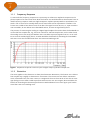
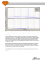
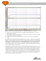
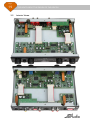
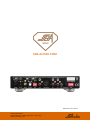
Thoughts about the Design of the ADICON
SSB Audio GmbH
Sonnenweg 25 – 30827 Garbsen – Germany
www.ssb-audio.com
Page
1
THOUGHTS ABOUT THE DESIGN OF THE ADICON
N
Contents
1
Introduction ........................................................................................................................................ 1
1.1
Which Data Should Be Discussed ......................................................................................... 1
1.1.1
Frequency Response ............................................................................................................... 2
1.1.2
Distortion .................................................................................................................................. 2
1.1.3
Noise ......................................................................................................................................... 3
2
Circuit description .............................................................................................................................. 5
2.1
Phono Preamplifier ................................................................................................................. 5
2.1.1
Frequency Response ............................................................................................................... 6
2.1.2
Noise ......................................................................................................................................... 8
2.2
Line Inputs .............................................................................................................................. 12
2.2.1
Volume Control vs. Gain Control ......................................................................................... 12
2.2.2
Line Input Sensitivity and Gain Range, Signal Leveling .................................................... 15
2.3
Headphone Output ............................................................................................................... 15
2.4
ADC .......................................................................................................................................... 16
2.5
Peak Program Meter ............................................................................................................. 16
2.6
Power supply ......................................................................................................................... 16
3
Housing ............................................................................................................................................. 18
3.1
Front Panels ........................................................................................................................... 18
3.2
Interior Views ......................................................................................................................... 19
1 Introduction
There are many rumors how to design analog circuits like e.g. RIAA equalization amplifiers, ADCs,
headphone amplifiers and more. Many of them may be fairy tales, others true. Here I’d like to
explain why the design of the ADICON is like it is.
First of all you should know my “Uwe’s Opinion about the Sound of Electronics”, and then you
may understand why I do not care for extra expensive resistors or capacitors. Instead, I assure
that all components fulfill their requirements either virtually ideal or, regarding their cost, adequately. And you will understand that I look for technical data and not for some kind of special
sound because there must not be any special sound. This device has to be neutral.
1.1
Which Data Should Be Discussed
Technical data predominantly means: Frequency response (consisting of amplitude response and
phase response), distortion and noise performance. There are more data that can be measured
and specified, but I think for a device like this they are negligible in an amount that talking about
them would be beyond the scope of this article.
Page
2
THOUGHTS ABOUT THE DESIGN OF THE ADICON
N
1.1.1
Frequency Response
To start with the frequency response: It is quite easy to achieve an amplitude response and a
phase response far more linear than what the human ear would be able to discriminate from an
ideal frequency response. With one slight exception: A phono preamp with its equalization network is not so close to be virtually ideal, but I’ll come back to that. Expressed in numbers: The
human ear is able to hear about 20 Hz to 20 kHz. The signal sources we use, i.e., tape recorders
and turntables, do not deliver more bandwidth either, at least not significantly more.
The process of converting the analog to a digital signal implies the need to limit the bandwidth to
at least half the sample rate, e.g., less than 100 kHz at 192 kHz sample rate. On the other hand,
the analog circuits are easily and without extra cost able to process signals from 0.1 Hz or even
DC to several 100 kHz highly linear. So what would be the benefit of extending this bandwidth
with extra cost? You’ll understand that I am convinced: Nothing at all.
Figure: Amplitude response from line input to digital output @ 96 kHz sample rate
1.1.2
Distortion
The same applies to the distortion or THD (Total Harmonic Distortion). The human ear is able to
hear maybe very roughly 1% distortion in sine waves. The sources we use deliver sometimes
more, sometimes less, but none is even in a magnitude close to the 0.001% or less that an average analog circuit or ADC is able to perform without extra cost. Once again, what would be the
benefit of extending this distortion performance with additional cost? Once again you’ll understand that I am sure: Nothing at all.
Page
3
THOUGHTS ABOUT THE DESIGN OF THE ADICON
N
Figure: Total harmonic distortion and crosstalk from line input to digital output @ 96 kHz sample rate (The 50 Hz hum and its harmonics in the left channel result from an unscreened
part of the 1 kHz generator and were disregarded during this measurement)
1.1.3
Noise
The noise performance is a little bit different. The human ear has a dynamic range of about
140 dB. That is a factor of 1 : 10,000,000 (10 million!) and that is more than the best audio-ADC is
able to deliver. Thus it seems to be plausible to request a dynamic range as high as possible in
order to surpass the human ear’s capability. Unfortunately our good old signal sources once
again by far do not deliver as much as that. Maybe 60 dB, possibly 70 dB, that is a mere factor of
1 : 1000 up to 1 : 3000.
The ADICON’s dynamic range is about 110 dB (1 : 300,000) when the line inputs are used. That is
obviously much more than necessary. But with an appropriately good signal source the signal
chain’s dynamic range can be maintained that high. Yet this high value is still less than what
humans can hear. This is why I believe it is worth having a closer look on the noise performance
and, admittedly, I regard this to be a sporty challenge.
The following picture shows the noise performance of the ADICON limited to the audible frequency range of 20 Hz to 20 kHz. The inputs were terminated with low impedance for the measurement.
Page
4
THOUGHTS ABOUT THE DESIGN OF THE ADICON
N
Figure: Dynamic range and noise spectrum of the ADICON, limited to 20 Hz to 20 kHz
The top curve shows the noise spectrum of the MM (moving magnet) phono input at full
sensitivity (gain = +20 dB).
The two curves below show the noise spectra of both line inputs, again at full sensitivity (gain
= +20 dB). Both are identical as expected.
The bottom curve shows the noise spectrum of a line input at minimum sensitivity (gain =
-10 dB).
The assignment “Overall Level” refers to the bottom curve, i.e. gain = -10 dB, and means that the
ADICON’s dynamic range referred to the frequency range of 20 Hz to 20 kHz is 109.7 dB approximately. This is not quite as much as the 111 dB that would at best be reached with the used ADC
according to its data sheet and is because the analog preamplifier and the anti-alias filter stage
contribute about 1.5 dB to the noise floor. At 0 dB gain the dynamic range is reduced to about
109.0 dB and at a gain = +20 dB it decreases by almost 11 dB to about 99 dB. Read more in chapter 2.2.1 ”Volume Control vs. Gain Control”.
Incidentally, it is not trivial to obtain spectra in which individual interference frequencies, e.g. of
the switching regulator and other potentially interfering circuit parts, still are below the extremely
low detection limit here. In the case of the MM input with additional +20 dB of gain, the gain is
between almost 80 dB and 40 dB and the detection limit is correspondingly between -80 dB and
-120 dB, so that the potential interference frequencies are more than 160 dB below 2 VRMS and
thus have to be less than 20 nVRMS (0.000,000,02 V). In the case of line inputs with +20 dB gain the
detection limit is -132 dB, so that the interference frequencies are more than 152 dB below
2 VRMS, so they have to be less than 50 nVRMS.
Page
5
THOUGHTS ABOUT THE DESIGN OF THE ADICON
N
2 Circuit description
Figure: Block circuit of the ADICON
2.1
Phono Preamplifier
The phono preamplifier, also called RIAA pre-amp or RIAA equalizer, can be inserted into the
signal path of Input 1. It has two tasks: It has to amplify the pickup’s low output voltage and it has
to convert or equalize the non-linear frequency response to a linear one. The frequency response
that is applied when a vinyl is recorded is precisely defined by the RIAA. It is such that high frequencies are amplified much, much more than low ones. Thus during playback low frequencies
need to be much, much more amplified than high ones.
Later, the EIA recommended another equalization curve for playback which introduces an additional 20 Hz high-pass filter. Their idea was that below 20 Hz only rumble noise would appear and
it would be more advisable to reduce that noise instead of sticking devotedly to the RIAA curve.
To not only my point of view this is a very good idea. But as I assume that the ADICON will be
operated with high-quality turntables which feature significantly less rumble noise I think it is
appropriate to lower the high-pass filter’s corner frequency significantly down to about 7 Hz.
Page
6
THOUGHTS ABOUT THE DESIGN OF THE ADICON
N
Figure: RIAA-Curves
Red graph: The original RIAA equalization frequency response
Green graph: The EIA’s recommendation (20 Hz high-pass filter added)
Blue graph: The ADICON’s preamp frequency response (7 Hz high-pass filter)
2.1.1
Frequency Response
The phono preamplifier in the ADICON is a single stage amplifier with the equalization network in
its feed-back path. This equalization network is precisely calculated. The effect of deviation of the
component’s values from nominal values can easily be calculated. Due to the precision of metal
film resistors and C0G capacitors the frequency response can be guaranteed not to deviate more
than +/- 0.5 dB from ideal within the audible band (20 Hz to 20 kHz).
Page
7
THOUGHTS ABOUT THE DESIGN OF THE ADICON
N
Figure: Deviation from the targeted frequency response using a 10 run Monte Carlo simulation
with 5% capacitors and 1% resistors
The capacitive load issue: Anyway, these deviations are small and negligible compared to
another effect that exists with MM pickups. Due to their intrinsic inductance and capacitance
these pickups also show a significant loss of high frequencies and/or resonance. A simulation
shall explain the effect.
The following circuit diagram assumes a pickup with 470 mH inductance and 1.6 kΩ ohmic series
resistance. The capacitive load C2 is the sum of the winding and cable capacitance and an external load capacitance and will be varied in the simulation. R2 is the usual load resistance in phono
preamps.
Figure: Equivalent circuit diagram for an MM pickup. C2 is composed of the winding, cable and
external load capacitance. R2 is the preamplifier’s input impedance.
It can be seen that the frequency response is influenced and can be optimized by C2:
Page
8
THOUGHTS ABOUT THE DESIGN OF THE ADICON
N
Figure: Different frequency responses resulting from different load capacitances
This is why pickup manufacturers suggest a certain external load capacitance for an optimal
frequency response and why the ADICON’s MM preamplifier provides such an adjustable load
capacitance.
Unfortunately it is not trivial to find the correct capacitance setting even when the suggested load
is known, because a) the cable capacitance is unknown and b) some turntables already incorporate the recommended capacitors.
Cable capacitances vary from less than 100 pF/m for low-capacitance cables suitable for MM
pickups up to more than 500 pF/m for simple RCA-cables. When this capacitance is unknown, you
cannot determine without special equipment which external load capacitance needs to be set for
an optimal result.
Therefore it can be realized that MM phono cables should never be extended.
2.1.2
Noise
I laid an extra eye on the noise performance of the ADICON because this is closer to be critical
than many other items in the ADICON’s design.
Noise is produced by the preamplifier’s non-ideal input stage and can be characterized as an
amount of voltage applied to the preamplifier’s input with an assumed ideal (i.e. noise-less) input
stage. Thus it is often referred as “input referred noise”.
It seems obvious to design such a preamplifier with the lowest possible noise. But it’s not as easy
as that.
Page
9
THOUGHTS ABOUT THE DESIGN OF THE ADICON
N
Firstly, you need to consider that not only the preamplifier, but also the pickup itself produces
noise. This is due to the ohmic resistance of its winding. Each ohmic resistor produces noise, the
so-called thermal or Johnson noise.
If the input stage works with bipolar transistors, you need to consider that the preamplifier’s
noise is not only caused by the mentioned input voltage noise, but also by an input current noise
generated by the preamplifier’s input stage. When the input is connected to ground, this current
does not produce any noise, but when the input is terminated with any impedance (ohmic, resistive or capacitive), another noise voltage arises. The pickup connected to the input is such an
impedance.
Thus the total input referred noise is the sum of
1. the pickup’s Johnson noise,
2. the preamplifier’s input voltage noise and
3. the preamplifier’s input current noise multiplied by the pickup’s impedance.
Talking about the sum: Whenever voltages of independent noise sources are to be summed up it
is not just the simple sum of all voltages (U1 + U2 +…+ UN, called arithmetic sum). Instead, it is the
square root of the sum of the squares of all three voltages (SQRT(U1² + U2² +…+ UN²), called geometric sum).
Finally, the total input referred noise is
a. weighted by the preamplifier’s RIAA equalization curve, i.e., low frequencies are much more
amplified than high frequencies, and
b. weighted by the human ear’s spectral sensitivity, usually represented by the A-weighting
curve.
Next, we also need to discriminate between MM (moving magnet) and MC (moving coil) pickups.
Moving Magnet Pickups typically have a winding resistance, inductance and capacitance of
1.5 kΩ, 500 mH and 100 pF, but that can vary a lot. In practice, all three noise sources listed
above matter.
The spectra of the pickup’s Johnson noise and the preamplifier’s input voltage noise are both
white. But the input current induced noise is not white: For low frequencies it is dominated by the
winding’s resistance, for high frequencies it is dominated by the winding’s inductance.
Let’s sum up:
You cannot reduce or influence the pickup’s Johnson noise by the design of the preamplifier.
By design you have influence on the preamplifier’s input voltage and current noise and thus
means for optimization.
Particularly due to the geometric summation it makes little sense to spend a lot of effort in
order to reduce the preamplifier’s input noise far below the pickup’s Johnson noise.
In practice it really makes sense to spend some effort on the noise performance. With an appropriate input circuit it is possible to keep the preamplifier’s noise decently below the pickup’s
Johnson noise. And, not to forget, this is very far below the noise coming from the vinyl itself.
Often the very low noise op-amp AD797 is used for this application. But this expensive op-amp is
optimized for low input voltage noise, not for low input current noise. The effect is counterproductive, as the diagram below demonstrates:
Page
10
THOUGHTS ABOUT THE DESIGN OF THE ADICON
N
Figure: Three noise sources for the example of an AD797 combined with an MM pickup,
weighted by the RIAA equalization curve and the ANSI-A curve
The AD797’s input voltage noise is significantly lower than the pickup’s Johnson noise, but the
input current induced noise is significantly higher, particularly in the most audible area.
It is a technological phenomenon that low voltage noise op-amps suffer from high input current
noise. Thus it is wise to select an op-amp with the optimal compromise between both kinds of
noise. The OPA227 is one of those:
Page
11
THOUGHTS ABOUT THE DESIGN OF THE ADICON
N
Figure: Three noise sources for the example of an OPA227 combined with an MM pickup,
weighted by the RIAA equalization curve and the ANSI-A curve
The OPA227’s input voltage noise is higher than the AD797’s one but still lower than the pickup’s
Johnson noise. On the other hand, the input current induced noise is significantly lower, particularly in the area where the human ear is most sensitive.
Moving Coil Pickups have typically a winding resistance of a few ohms and their inductance and
capacitance are so low that they can be neglected, see the diagram below. Thus in practice, only
the preamplifier’s input voltage noise matters.
In practice, in these kinds of applications another noise source matters: The feed-back network
has an output impedance that must also not be neglected. For example, when the feed-back
network’s impedance is the same as the pickup’s impedance, it generates as much noise as the
pickup itself.
Page
12
THOUGHTS ABOUT THE DESIGN OF THE ADICON
N
Figure: Three noise sources for the example of an AD797 combined with an MC pickup,
weighted by the RIAA equalization curve and the ANSI-A curve
The AD797 is clearly the best choice in this case even though its noise is still approximately twice
as high as the pickup’s noise and still significantly higher than the pickup’s noise plus the feedback network’s noise.
The best but most expensive solution is to use transformers in order to convert the pickup’s
impedance and output voltage to a value where succeeding amplifiers can easily be designed
with negligible noise. Transformers do not introduce (appreciable) noise, except possibly hum
from magnetic fields in their environment. The transformer’s outputs can usually be directly
connected to MM inputs.
2.2
Line Inputs
The line inputs use OPA2134 FET audio operational amplifiers. Once again, the performance
concerning frequency response and distortion is by far superior to the human ear and also superior to the ADC-IC. And once again, a special eye should be laid on its noise performance.
2.2.1
Volume Control vs. Gain Control
It leaps to the eye that with the gain control potentiometers in the ADICON it is not possible to
reduce the input signal down to zero. Instead, you can attenuate the input signal by 10 dB or
amplify it by up to 20 dB only, i.e., the whole gain control range is 30 dB. This does not correspond to what you know from tape recorders.
Page
13
THOUGHTS ABOUT THE DESIGN OF THE ADICON
N
Volume Control: I call the characteristic of the potentiometers used there “Volume Control”, i.e.,
you can completely fade-out the input signal. The circuit looks like this:
Figure: Volume Control circuit
In the Volume Control circuit all signals are attenuated at first and afterwards amplified with a
fixed gain.
Would I use such a characteristic in the ADICON, too, the effect on its noise performance would
be a kind of a catastrophe because the necessary gain of the amplifier together with its input
noise would significantly exceed the ADC-IC’s input noise and thus significantly reduce the systems noise performance or dynamic range.
Gain Control: I use a circuit that I call “Gain Control” instead:
Figure: Gain Control circuit
In the Gain Control circuit the amplifier’s gain is not fixed and may be even below 1. The noise
generated by this circuit exceeds the ADC-IC’s noise only at high gains, which can never be
avoided, of course.
The consequences in practice can be visualized in the diagram below:
Page
14
THOUGHTS ABOUT THE DESIGN OF THE ADICON
N
Figure: Different noise performance using volume or gain control
The blue graph is the ADC’s dynamic range of 111 dB (unweighted). This is the system’s
bottleneck which cannot be circumvented.
The green graph is the input preamp’s dynamic range referred to the ADC-IC’s 100% FS input
level at different gain settings when the gain control schematics is used. The green dotted line is
the resulting overall dynamic range of such a system.
The red graph is the input preamp’s dynamic range referred to the ADC-IC’s 100% FS input level
at different gain settings when the volume control schematics is used. The red dotted line is the
resulting overall dynamic range of such a system.
Theory and practice: The above curves are calculated theoretically. However, in practice the
analog preamplifiers increase the noise floor of the ADC by a little more than 1 dB, which was not
included in the above calculation. Otherwise, the theoretical values square relatively well with the
measured results shown in chapter 1.1.3 “Noise” and correspond to the left and the right end of
the green dashed curve: For the theoretically resulting 110.9 dB in practice about 109.7 dB were
reached at a gain = -10 dB. At a gain = 0 dB the theoretically resulting 0,7 dB less were measured
as well, only at a gain = +20 dB the measured 99 dB were not only the expected 8 dB less, but
almost 11 dB less.
Conclusion: The preamplifier’s input noise unavoidably decreases the noise performance at high
gains in both cases, but for low gains the noise performance with the Gain Control circuit is
significantly better.
In principle with a Gain Control circuit using a negative logarithmic potentiometer a widely logarithmic control range of 0 to 100% gain, like in the above Volume Control circuit, can be obtained,
too, but without its disadvantageous noise performance. However logarithmic potentiometers
have a clearly poorer synchronization than linear ones, so I preferred to forego a control range
down to 0% gain in favor of a more precise synchronization. That is why the gain characteristic
(gain vs. potentiometer position) for the Gain Control circuit in the ADICON looks like this:
Page
15
THOUGHTS ABOUT THE DESIGN OF THE ADICON
N
Figure: The ADICON’s gain potentiometer characteristic
This characteristic is not perfectly correct because a strictly linear potentiometer is assumed. A
real linear potentiometer has a slightly flattened slope at both ends.
2.2.2
Line Input Sensitivity and Gain Range, Signal Leveling
RCA Outputs: The output voltage of most CD or DVD players is 2 VRMS for 100% FS (Full Scale, the
maximally possible value of a digital signal). On many CDs this full scale range is completely used,
other CDs use considerable headroom so that they sound significantly quieter. This is why the
ADICON’s nominal line input sensitivity for 100% FS is 2 VRMS and the line output delivers 2 VRMS at
100% FS, too.
Tape recorders can usually be adjusted in a wide range including 2 VRMS. The output voltages of
phono preamps are similar but additionally depend on the cartridge’s sensitivity and the modulation of the record.
DIN Outputs: The output voltage at DIN outputs is usually slightly lower, particularly with very
old devices.
When analog signals are to be digitized they need to be leveled decently. That means, that under
no circumstances the ADC should clip. On the other hand, they should “sound” as loud as other
average digital sources, so the digital level should not be too low.
For these reasons the gain for the line and phono inputs need to be adjustable. In the ADICON
the gain range of -10 dB to +20 dB is provided so that signals from 0.2 VRMS up to 6 VRMS can be
leveled to 100% FS.
2.3
Headphone Output
With 7 VRMS at 50 Ω output impedance the headphone output power is significantly higher than
that usually found in other hi-fi equipment. A relay mutes the output at switching on or off.
The headphone amplifier essentially consists of a TPA6120, a powerful headphone amplifier IC.
This IC has a little weakness, namely its input noise. It is a bit too large to amplify the signal avail-
Page
16
THOUGHTS ABOUT THE DESIGN OF THE ADICON
N
able of 2 VRMS directly, without the noise becoming audible too clearly. Therefore, a separate
10 dB preamplifier was used for the TPA6120.
The gain of the headphone amplifier was chosen so that it doesn’t overdrive as long as the red
CLIP LEDs are not on. Strictly speaking this is true only for headphone impedances greater than
about 300 Ω, as normally found on headphones for hi-fi systems. Headphones for professional
applications often have considerably lower impedances. But even with these the output signal
remains undistorted at modulations up to -1 dB approximately.
2.4
ADC
In the course of the recent years I have developed and refined several ADC circuits. The circuit of
nd
the ADICON is another offshoot of them. Its anti-alias filter is a balancing 2 order low-pass
Butterworth filter with a corner frequency of 190 kHz approx., that easily inhibits any alias effects.
The Cirrus Logic CS5361 is a high quality 114 dB (A-weighted) delta sigma A/D converter. The
clock of the CS5361 is derived from two crystal oscillators. A CPLD (complex programmable logic
device) provides the control functions and serves as clock divider for the CS5361.
The S/PDIF-Transmitter CS8406 is also controlled by the CPLD. It drives an optical, Toslinkcompatible output and a coaxial RCA output. The RCA output is transformer coupled in order to
avoid ground loops.
2.5
Peak Program Meter
The level of the digitized signal needs to be indicated clearly. A stereo sample peak program
meter (SPPM) according to the EBU specifications with 2 x 10 LEDs is provided for that. This SPPM
is implemented fully digital within the CPLD already mentioned above.
The brightness of the display can be adjusted in four stages with two DIP switches on the back so
that in the weakest level it does not interfere even at very subdued room lighting and in the
strongest level it is clearly recognizable even at very bright room lighting.
In contrast to standard PPMs which have an attack time of 10 ms an SPPM’s attack time is one
sample only. This allows to exactly determine the digital output signal’s peak levels. The decay
time of PPMs and SPPMs is 20 dB in 1.5 s. A peak hold function can be added to the displayed
level. Refer to the user manual for hints on correct leveling.
BTW, the characteristic of the VU meters commonly used in tape recorders is completely different from that of PPMs or SPPMs. Such a VU meter would not be very helpful for an ADC while
conversely a PPM would not be appropriate for a tape recorder.
2.6
Power supply
The ADICON is supplied by 12 DC. A common 2.1/5.5 mm plug can be used. In order to prevent
accidental disconnection the power supply’s bayonet plug can be locked by twisting it. The on/off
switch is on the backside. I would rather have seen it on the front panel, but I did not have to
Page
17
THOUGHTS ABOUT THE DESIGN OF THE ADICON
N
decide alone. The front panel should be designed completely symmetrical. That would not have
been possible with the switch on the front panel. Therefore, we decided to move it to the back.
We hope for your understanding for this decision.
An internal overvoltage protection switches the ADICON off when supply voltages of more than
14 V are applied. Voltages above 20 V must be avoided. Also, there is a reverse polarity protection
for the power supply.
The internal 3.3 V switch-mode down converter for the digital circuitry is clearly segregated from
the remaining circuit so that no remaining switch noise is visible in the spectrum.
The negative voltage supply is quite unique: Two charge pump ICs working in push-pull mode
provide the negative supply voltage for the analog section. This reduces the ripple current from
the positive and the ripple voltage on the negative supply enormously. Moreover, both ICs are
controlled by the FPGA and work synchronously to the ADC’s sample rate. As a result residual
noise would be removed from the transmission spectrum, if it would even exist yet. But as it does
not do, this measure is actually superfluous. Anyway, on the one hand it was a precautionary
measure, because this situation was not foreseeable from the outset, and on the other hand this
measure costs almost nothing- except the time to develop -, and it's worth it to me in any case.
Page
18
THOUGHTS ABOUT THE DESIGN OF THE ADICON
N
3 Housing
The housing was designed by Sonny. He is the one of us with a lot of experience in the design of
(in my opinion) excellent looking, very precisely manufactured and economically producible
housings. He decided on a sturdy sheet steel case which shields magnetic fields much better than
aluminum cases, for example.
3.1
Front Panels
The 5 mm thick aluminum front panel has a special surface. It is not just anodized, it is treated in
a special way that only very few manufacturers can provide with reliable quality. Because we are
not sure if a black or silver front plate proves more popular, we have decided to offer both.
Figures: Front panels in silver and black
Page
19
THOUGHTS ABOUT THE DESIGN OF THE ADICON
N
3.2
Interior Views
SSB-AUDIO.COM
Uwe Beis, 2015-05-19
SSB Audio GmbH
Sonnenweg 25 – 30827 Garbsen – Germany
www.ssb-audio.com