1
Analog input/
output module
User’s Manual
(Hardware)
A1S63ADA
Thank you for buying the Mitsubishi general-purpose programmable
logic controller MELSEC-A Series
Prior to use, please read both this manual and detailed manual
thoroughly and familiarize yourself with the product.
MODEL A1S63ADA-U-(H/W)
MODEL
13JG43
CODE
IB(NA)-68474-H(1112)MEE
©1994 MITSUBISHI ELECTRIC CORPORATION
z SAFETY PRECAUTIONS z
(Read these precautions before using this product.)
Before using this product, please read this manual and the relevant manuals
carefully and pay full attention to safety to handle the product correctly.
These precautions apply only to this equipment. Refer to the CPU module user's
manual for a description of the PC system safety precautions.
In this manual, the safety precautions are classified into two levels:
" WARNING" and " CAUTION".
Under some circumstances, failure to observe the precautions given under
" CAUTION" may lead to serious consequences.
Observe the precautions of both levels because they are important for personal
and system safety.
Make sure that the end users read this manual and then keep the manual in a
safe place for future reference.
[DESIGN PRECAUTIONS]
WARNING
z Configure a safety circuit on the outside of the PC so that the entire system
works to a safe side even when the external power failure occurs or PC main
unit fails.
An erroneous output or operation may result in an accident.
CAUTION
z Use the PC in the environment given in the general specifications section of
the applicable CPU module user's manual.
Failure to do so may result in electric shock, fire, or erroneous operation or
may damage or degrade the equipment.
z Do not bundle, or install, the control cables with, or near, the main circuit and
power cables.
Keep them at least 100 mm (3.9 inch) away from such cables.
Noise may cause erroneous operation.
z At power ON/OFF, voltage or current may instantaneously be output from the
output terminal of this module. In such case, wait until the analog output
becomes stable to start controlling the external device.
A-1
[INSTALLATION PRECAUTIONS]
CAUTION
z Insert the tabs at the bottom of the module into the holes in the base module
before installing the module. Be sure to install the module in the base
module with screws tightened to the specified torque.
Improper installation may cause erroneous operation, accident, or the
module to fall out.
z Do not directly touch the module's conductive parts or electronic
components.
Doing so could cause malfunction or trouble in the module.
[WIRING PRECAUTIONS]
CAUTION
z If noise generates frequently, ground the AG and FG terminals using the PC
dedicated class-D ground (class-three ground) or higher.
Failure to do so may result in erroneous operation.
z Confirm the rated voltage and terminal arrangement of the module before
wiring it to the PC.
If a power supply of different rating is connected or a wiring is performed
erroneously, fire or accident may result.
z Tighten the terminal screws to the specified torque.
Loose terminal screws may cause a short circuit or erroneous operation.
If excessively tightened, the terminal screws may be damaged, and cause a
short circuit or erroneous operation.
z Be sure that cuttings, wire chips, or other foreign matter do not enter the
module.
Foreign matter may start a fire or cause an accident or erroneous operation.
A-2
[STARTING AND MAINTENANCE PRECAUTIONS]
CAUTION
z Do not touch live terminals.
It may cause erroneous operation.
z Be sure to shut off all phases of the external power supply used by the
system before cleaning or retightening the terminal screws.
Not doing so can cause the module to fail or malfunction.
z Do not disassemble or rebuild the module.
It may cause accidents, erroneous operation, injury, or fire.
z Be sure to shut off all phases of the external power supply used by the
system before mounting or removing the module.
Not doing so may cause damage to the module.
z Do not install/remove the terminal block more than 50 times after the first use
of the product. (IEC 61131-2 compliant)
z Before handling the module, always touch grounded metal, etc. to discharge
static electricity from the human body.
Failure to do so may cause the module to fail or malfunction.
[OPERATING PRECAUTIONS]
CAUTION
z Do not output (ON) "Use Prohibited" signals from the PC CPU to the special
module.
Doing so could erroneously operate the PC system.
[DISPOSAL PRECAUTIONS]
CAUTION
z When disposing of this equipment, handle it as industrial waste.
A-3
z CONDITIONS OF USE FOR THE PRODUCT z
(1) Mitsubishi programmable controller ("the PRODUCT") shall be used in
conditions;
i) where any problem, fault or failure occurring in the PRODUCT, if any, shall
not lead to any major or serious accident; and
ii) where the backup and fail-safe function are systematically or automatically
provided outside of the PRODUCT for the case of any problem, fault or failure
occurring in the PRODUCT.
(2) The PRODUCT has been designed and manufactured for the purpose of
being used in general industries.
MITSUBISHI SHALL HAVE NO RESPONSIBILITY OR LIABILITY
(INCLUDING, BUT NOT LIMITED TO ANY AND ALL RESPONSIBILITY OR
LIABILITY BASED ON CONTRACT, WARRANTY, TORT, PRODUCT
LIABILITY) FOR ANY INJURY OR DEATH TO PERSONS OR LOSS OR
DAMAGE TO PROPERTY CAUSED BY the PRODUCT THAT ARE
OPERATED OR USED IN APPLICATION NOT INTENDED OR EXCLUDED
BY INSTRUCTIONS, PRECAUTIONS, OR WARNING CONTAINED IN
MITSUBISHI'S USER, INSTRUCTION AND/OR SAFETY MANUALS,
TECHNICAL BULLETINS AND GUIDELINES FOR the PRODUCT.
("Prohibited Application")
Prohibited Applications include, but not limited to, the use of the PRODUCT
in;
y Nuclear Power Plants and any other power plants operated by Power
companies, and/or any other cases in which the public could be affected if
any problem or fault occurs in the PRODUCT.
y Railway companies or Public service purposes, and/or any other cases in
which establishment of a special quality assurance system is required by
the Purchaser or End User.
y Aircraft or Aerospace, Medical applications, Train equipment, transport
equipment such as Elevator and Escalator, Incineration and Fuel devices,
Vehicles, Manned transportation, Equipment for Recreation and
Amusement, and Safety devices, handling of Nuclear or Hazardous
Materials or Chemicals, Mining and Drilling, and/or other applications
where there is a significant risk of injury to the public or property.
Notwithstanding the above, restrictions Mitsubishi may in its sole discretion,
authorize use of the PRODUCT in one or more of the Prohibited Applications,
provided that the usage of the PRODUCT is limited only for the specific
applications agreed to by Mitsubishi and provided further that no special
quality assurance or fail-safe, redundant or other safety features which
exceed the general specifications of the PRODUCTs are required. For details,
please contact the Mitsubishi representative in your region.
A-4
REVISIONS
Print Date
Oct.,1994
Feb.,1999
Dec.,1999
Nov.,2001
Oct.,2002
Sep.,2005
Sep.,2006
Dec.,2011
The manual number is given on the bottom right of the front cover.
Manual Number
Revision
IB (NA)-68474-A
First edition
IB (NA)-68474-B
Addition
Safety precautions
Partial Correction
Section 3.1
IB (NA)-68474-C
Partial Correction
Chapter 2
IB (NA)-68474-D
Partial Correction
Contact ad dress (Back cover)
IB (NA)-68474-E
Partial Correction
Chapter 2, Section 5.2
IB (NA)-68474-F
Addition
Conformation to the EMC Directive and
Low Voltage Instruction
Partial Correction
SAFETY PRECAUTIONS
IB (NA)-68474-G
Partial Correction
SAFETY PRECAUTIONS
IB (NA)-68474-H
Addition
SAFETY PRECAUTIONS (Chinese),
CONDITIONS OF USE FOR THE
PRODUCT
This manual confers no industrial property rights or any rights of any other kind,
nor dose it confer any patent licenses. Mitsubishi Electric Corporation cannot be
held responsible for any problems involving industrial property rights which may
occur as a result of using the contents noted in this manual.
© 1994 MITSUBISHI ELECTRIC CORPORATION
A-5
CONTENTS
Safety Precautions ························································································· A-1
Revision History ····························································································· A-5
Contents········································································································· A-6
About the Manuals ························································································· A-7
1. OVER VIEW···································································································1
2. PERFORMANCE SPECIFICATIONS·····························································1
3. NAMES AND SETTINGS OF EACH PART ····················································4
3.1 Names of each part ··················································································4
3.2 Setting the offset and gain ········································································7
4. HANDLING ··································································································10
4.1 Precautions for handling. ········································································10
5. WIRING········································································································11
5.1 Precautions for wiring ·············································································11
5.2 Example of module connection ·······························································11
6. OUTLINE DIMENSION DRAWINGS ····························································13
A-6
About the Manuals
The following manuals are related to this product.
Order them if necessary.
Detailed manuals
Manual Name
Analog input/output module type A1S63ADA
User's Manual.
Manual No.
(Model code)
IB-66435
(13JE30)
COMPLIANCE WITH EMC AND LOW VOLTAGE DIRECTIVES
(1) Method of ensuring compliance
To ensure that Mitsubishi programmable controllers maintain EMC and
Low Voltage Directives when incorporated into other machinery or
equipment, certain measures may be necessary. Please refer to one of the
following manuals.
y User's manual for the CPU module used
y User's manual (hardware) for the CPU module or base unit used
The CE mark on the side of the programmable controller indicates
compliance with EMC and Low Voltage Directives.
(2) Additional measures
No additional measures are necessary for the compliance of this product
with EMC and Low Voltage Directives.
A-7
1. OVERVIEW
This manual describes specifications, handling and wiring of an A1S63ADA
Analog input/output module (hereinafter referred to as the A1S63ADA).
2 PREFORMANCE SPECIFICATIONS
The performance specifications of the A1S63ADA are shown below.
D-A conversion
A-D conversion
Item
Specifications
Voltage:-10 to 0 to 10VDC(input resistance: 1MΩ)
Analog input
Current:-20 to 0 to 20mADC(input resistance: 250Ω)
-4096 to 4095 (when resolution is set to 1/4000)
Digital output
-8192 to 8191 (when resolution is set to 1/8000)
-12288 to 12287 (when resolution is set to 1/12000)
Digital value output
Analog input
1/4000
1/8000
1/12000
I/O
10V
4000
8000
12000
characteristics 5V or 20mA
2000
4000
6000
*1
0V or 4mA
0
0
0
-5V or –20mA
-2000
-4000
-6000
-10V
-4000
-8000
-12000
2.5mV
1.25mV
0.83mV
Voltage
Max. resolution
10 A
5 A
3.33 A
Current
Conversion
1ms/ch
2ms/ch
3ms/ch
speed
General
1%
40
80
120
accuracy*2
Absolute max.
Voltage: 15V Current: 30mA*3
input
Analog input
2 channel
points
Voltage output
Current output
-4000 to 4000
0 to 4000
(when resolution is set to 1/4000) (when resolution is set to 1/4000)
-8000 to 8000
0 to 8000
Digital input
(when resolution is set to 1/8000) (when resolution is set to 1/8000)
-12000 to 12000
0 to 12000
(when resolution is set to 1/12000) (when resolution is set to 1/12000)
-10 to 0 to 10VDC(external load
0 to 20mADC(external load
Analog output
resistance:2kΩ to 1MΩ)
resistance:0Ω to 600Ω)
Analog
Analog
1/4000 1/8000 1/12000 output 1/4000 1/8000 1/12000 output
value
value
I/O
4000
8000
12000
10V
4000
8000
12000
20mA
characteristics
2000
4000
6000
5V
2000
4000
6000
12mA
*4
0
0
0
0V
0
0
0
4mA
-2000 -4000
-6000
-5V
-4000 -8000 -12000
-10V
5 A
Max. 1/4000 2.5mV
2.5 A
reso- 1/8000 1.25mV
lution 1/12000 0.83mV
1.7 A
1
Item
Specifications
Voltage output
D-A
conversion
Conversion
speed*5
General
accuracy*6
Solute max.
output
Output shorting
protection
Analog output
points
Common to
A-D and
D-A
conversions
1ms(1/4000) 2ms(1/8000) 3ms(1/12000)
1%(
Voltage:
0.1V)
1%(
12V
Current:
Conversion speed in simple
loop control*7
Number of occupying I/O
points
Connection terminal block
Applicable wire size
Applicable crimp terminal
0.2mA)
28mA
Provided
1channel
Specific
isolated area
Isolation
specifications
Current output
Isolation
method
Dielectric
withstand
voltage
Insulation
resistance
5MΩ or more
Between I/O
500V AC
terminal and Photocoupler
(measured with a
for 1
PLC power
isolation
minute 500V DC insulation
supply
resistance tester)
Between
Not isolated
channels
4ms(1/4000) 7ms(1/8000) 9ms(1/12000)
32 points
20-point terminal block (M3.5 7 screw)
0.75 to1.5mm2
1.25-3.5 1.25-YS3A 2-3.5 2-YS3A
V1.25-M3 V1.25-YS3A V2-3.5 V2-YS3A
Internal current consumption
0.8A
(5 VDC)
Weight
0.3kg
The offset and gain are set as shown below as the default setting.
CH1 ... Offset: 0V/4mA, Gain: 5V/20mA
CH2 ... Offset: 0V/4mA, Gain: 5V/20mA
CH3 ... Offset: 0V/4mA, Gain: 10V/20mA
*1: For offset value: 0V/4mA, gain value: 5V/20mA
*2: This is the accuracy in respect to the maximum digital output value. The maximum digital
output value is the maximum value at the selected resolution, and is the same for either a
current input or voltage input.
*3: Current value indicates value of instant input current that does not break module inner
electrical resistance.
*4: For offset value: 0V/4mA, gain value: 10V/20mA
*5: Depending on the timing of reading the digital value from the PLC CPU, the process may be
carried out with a delay of up to one conversion processing time. The response time for the
amplifier to output the D/A converted data to an external source is "maximum 1ms".
*6: This is the accuracy in respect to the maximum analog output value.
*7: The response time for the amplifier to output the D/A converted data to an external source is
"1ms". For the general specifications, refer to the User's Manual for the PLC CPU in use.
2
POINT
For approx. 30 minutes after the power is turned ON, the A/D conversion value will fluctuate due
to the effect of the self-generated heat.
If this fluctuation is a problem, start control after warming up for approx. 30 minutes. In the same
manner, wait approx. 30 minutes to warm up before adjusting the offset/gain value (user-set).
3
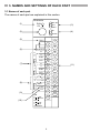
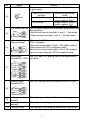
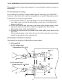
3. NAMES AND SETTINGS OF EACH PART
3.1 Names of each part
The names of each part are explained in this section.
A1S63ADA
OFF SET
RUN
CH
(1)
SET
(3)
GAIN
UP
(2)
(4)
DOWN
(5)
TEST
1
2
(6)
C
H
1
(7)
6
COM
C
H
2
I+
7
8
V+
COM
SLD
V+
C
H
3
V-
O
U
T
I-
I+
AG
FG
(9)
(10)
5
I+
SLD
A/D
4
V+
I
N
I
N
(8)
3
HLD/CLR
0
10V
0
20mA
D/A
0
10V
4 20mA
A1S63ADA
9
10
11
12
13
14
15
16
17
18
19
20
4
(11)
Name
RUN LED
23
Details
This indicates the A1S63ADA operation state.
• Normal mode
LED ON: In normal operation
Flickering: Setting data error
RUN
LED OFF: 5V power OFF or watch dog timer error
• Test mode
Flickering: The LED flickers at a 0.25 second
(1)
interval when the offset/gain select
switch is set to "OFFSET" or "GAIN". If
the CH3 setting value is set above the
setting range with the UP/DOWN switch,
the LED will flicker at a fast 0.1 second
interval.
LED OFF: The offset/gain select switch is set to
"SET".
Channel, resolution This sets the channel for adjusting the offset/gain
value and the resolution.
select switch
• Normal mode: Invalid
• Test mode : Valid
CH
(Factly setting: 0)
Setting
Offset/gain
90 1
Resolution
value
adjustment channel
1
CH1
1/14000
2
CH2
(2)
3
CH3
4
CH4
1/8000
5
CH5
6
CH6
7
CH7
1/12000
8
CH8
9
CH9
78
No.
5
4 6
Offset/gain select
switch
(3)
OFF SET
SET
GAIN
OFFSET position: The offset value is adjusted.
SET position : When moved from OFFSET to SET,
the offset value is registered.
When moned from GAIN to SET,
the gain value is registered.
GAIN position : The gain value is adjusted.
5
No.
Name
UP/DOWN switch
UP
(4)
DOWN
Details
This increments or decrements the CH3 offset value
or gain value.
Time at UP/DOWN
position
Less than 1.5s
1.5s or more
(5)
Increment/decrement
width
Voltage: approx. 2.5mV
Current: approx. 5 A
Voltage: approx. 50mV
Current: approx. 5 A
Test mode terminal This is used to adjust the offset/gain value and to set
the resolution.
TEST
• Short-circuit across terminals 1 and 3 ... Test mode
• Open across terminals 1 and 3 ... Normal mode
Output hold/clear
setting terminal
(6)
HLD/CLR
This sets the CH3 analog output state when the PLC
CPU is stopped.
Open across terminals 2 and 4: The offset value is
output when the CPU is stopped (clear)
Short-circuit across terminals 2 and 4: The analog
value is output when the CPU is stopped (hold)
Analog input
The CH1 and CH2 analog values (voltage/current)
terminal(CH1, CH2) are input.
V+
(7)
I+
C
H COM
1
SLD
V+
I+
C
H COM
2
SLD
Analog output
terminal(CH3)
(8)
C
H
3
V+
VI+
I-
Analog ground
terminal
Frame ground
(10)
terminal
(11) Terminal block
(9)
The CH3 analog values (voltage/current) is output.
This is the ground terminal for the analog signal.
This is the module's ground terminal.
The numbers in the drawing indicate the terminal No.
6
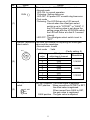
3.2 Setting the offset and gain
Use the following procedure to change the input/output conversion
characteristics.
Start
Apply the voltage or current to be
used as the offset value.
V
Short-circuit the test modeterminals (across 1 and 3).
V
COM
For voltage
TEST
V
For current
A
I
COM
(C)
Actually connected
resistance valuel
Set the "channel/resolution select
switch" to the No. of the channel
and resolution to be changed.
RUN
CH
Set the offset/gain select switch
to "OFF SET".
OFF
RUN
Set to the channel
and resolution to
be set.
OFF SET
SET
GAIN
Flickers
Set the offset/gain select switch
to "SET".
What channel is
to be adjusted?
CH3
(A)
RUN
OFF SET
SET
GAIN
OFF
CH1, CH2
(1)
7
(1)
(B)
Apply the voltage or current to be
used as the gain value.
Adjust other
channels?
V
V
YES
(C)
COM
NO
For voltage
V
For current
A
Open the test mode terminals
(across 1 and 3).
I
COM
TEST
Actually connected
resistance value
Set the offset/gain select switch
to "GAIN".
End *
RUN
Flickers
OFF SET
SET
GAIN
* The state of the RUN LED after the
adjustment is shown below.
Set the offset/gain select switch
to "SET".
RUN
OFF
RUN LED state
ON ... Adjustment was completed
normally.
OFF SET
SET
GAIN
Flicker ... The resolution is not the
same for all channels.
Adjust again.
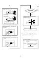
8
(2)
(A)
Set the offset/gain select switch
to "GAIN"
Set the offset/gain select switch
to "OFF SET".
OFF SET
SET
GAIN
RUN
Flickers
OFF SET
SET
GAIN
RUN
Flickers
Using the "UP/DOWN switch", set
the voltage or current to be used
as the offset value.
Using the "UP/DOWN switch", set
the voltage or current to be used
as the gain value.
V
V
For voltage
For
current
For voltage
V V
AI
For
current
COM
I
Actually connected
resistance value
COM
I
Set the offset/gain select switch
to "SET".
RUN
OFF SET
SET
GAIN
OFF
A I
Actually connected
resistance value
Set the offset/gain select switch
to "SET".
RUN
V V
OFF SET
SET
GAIN
OFF
(2)
(B)
9
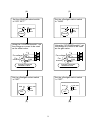
Remark
The offset value and gain values are set as follows.
(1) A/D conversion section
(a) The offset value is the analog input value (voltage or current) at which
the digital output value is "0".
(b) The gain value is the analog input value (voltage or current) at which the
digital output value is one of the following.
1. 2000 (resolution 1/4000)
2. 4000 (resolution 1/8000)
3. 6000 (resolution 1/12000)
(2) D/A conversion section
(a) The offset value is the analog value (voltage or current) output from the
A1S63ADA when the digital value is "0".
(b) The gain value is the analog value (voltage or current) output from the
A1S63ADA when the digital value is one of the following.
1. 4000 (resolution 1/4000)
2. 8000 (resolution 1/8000)
3. 12000 (resolution 1/12000)
4. HANDLING
4.1 Precautions for handling
(1) As the body case and terminal block are made of resin, do not drop these or
apply strong impacts.
(2) Do not remove the module's PCB from the case. Failure to observe this
could lead to faults.
(3) Make sure that foreign matter such as wire scraps do not enter the module
from the top while wiring. If any foreign matter enters, remove it.
(4) Tighten the module tightening screws and terminal screws, etc., within the
following range.
Screw position
Module tightening screw (M4 screw)
Terminal block terminal screw (M3.5 screw)
Terminal block installation screw (M4 screw)
10
Tightening torque range
78 to 118N • cm
59 to 88N • cm
78 to 118N • cm
5. WIRING
The precautions for wiring and examples of connecting the module are given in
this section.
5.1 Precautions for wiring
One condition for creating a highly reliable system and using the A1S63ADA
functions to the fullest is to carry out wiring that is not easily "affected by noise".
Precautions for wiring are given below.
(1) Use separate cables for the alternating current and A1S63ADA analog
input, and make sure that the alternating current side is not affected by
surge or induction.
(2) Do not wire near or with the main circuit wires, high-voltage wires or load
wire other than from the PLC. If laid close together, the wires will be
affected by noise, surge and induction.
(3) Ground the shield wire or the shield of the shield cable at one point on the
PLC side.
Note that depending on the state of noise from the external source, these
should be grounded on the external side.
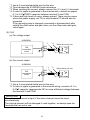
5.2 Example of module connection
The method for wiring the A1S63ADA is shown below.
(1) CH1 and CH2
(a) For voltage input
Signal source 0 to 10V
*4
15V
CH1
V
I
500k
250
500k
COM
SLD
15V
* 1 Shield
*2
(b) For current input
Signal source 0 to 20mA
CH2
*3
V
I
COM
SLD
* 1 Shield
*5
AG
FG
11
GND
500k
250
500k
*1: Use a 2-core twisted shield wire for the wire.
*2: This indicates the A1S63ADA input resistance.
*3: When inputting the current, always connect the (V+) and (I+) terminals.
*4: If noise or ripple is generated in the external wire, connect an approx.
0.1 to 0.47 F25WV capacitor between terminal V and COM.
*5: If there are high levels of noise, always ground. There may be cases
where the power supply unit FG or main module FG should also be
grounded.
If the grounding wire is changed (connected or disconnected) after
setting the offset value and gain value, set the offset value and gain
value again.
(2) CH3
(a) For voltage output
A1S63ADA
*1
D/A
conversion
circuit
*2
CH3
Motor drive unit, etc.
2k
V
V
to
GND 1M
(b) For current output
A1S63ADA
*1
D/A
conversion
circuit
CH3
I
I
*2
Motor drive unit, etc.
0
to
GND 600
*1: Use a 2-core twisted shield wire for the wire.
*2: If noise or ripple is generated in the external wiring, connect a 0.1 to
0.47 F capacitor (approximate 25V or more withstand voltage) between
the terminal V and COM.
IMPORTANT
The voltage and current output of the same channel cannot be used
simultaneously.
The internal element will be damaged if used together, so always open the
terminals that are not in use.
12
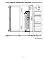
6. EXTERNAL DIMENSIONS DIAGRAM
A1S63ADA
RUN
CH
OFF SET
SET
GAIN
UP
130 (5.12)
DOWN
6.5
(0.26)
93.6
(3.69)
7.3
(0.29)
0
1
2
3
4
5
6
7
8
9
A
B
C
D
E
F
34.5
(1.36)
Unit: mm(inch)
13
MEMO
14
MEMO
15
WARRANTY
Mitsubishi will not be held liable for damage caused by factors found not to be the cause of
Mitsubishi; machine damage or lost profits caused by faults in the Mitsubishi products;
damage, secondary damage, accident compensation caused by special factors unpredictable
by Mitsubishi; damages to products other than Mitsubishi products; and to other duties.