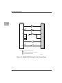
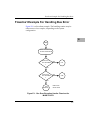
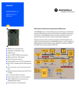
1
MVME133XTS VMEmodule
32-Bit Monoboard
Microcomputer
User’s Manual
VME133XTSA/IH1
Notice
While reasonable efforts have been made to assure the accuracy of this document,
Motorola, Inc. assumes no liability resulting from any omissions in this document,
or from the use of the information obtained therein. Motorola reserves the right to
revise this document and to make changes from time to time in the content hereof
without obligation of Motorola to notify any person of such revision or changes.
No part of this material may be reproduced or copied in any tangible medium, or
stored in a retrieval system, or transmitted in any form, or by any means, radio,
electronic, mechanical, photocopying, recording or facsimile, or otherwise,
without the prior written permission of Motorola, Inc.
It is possible that this publication may contain reference to, or information about
Motorola products (machines and programs), programming, or services that are
not announced in your country. Such references or information must not be
construed to mean that Motorola intends to announce such Motorola products,
programming, or services in your country.
Restricted Rights Legend
If the documentation contained herein is supplied, directly or indirectly, to the U.S.
Government, the following notice shall apply unless otherwise agreed to in
writing by Motorola, Inc.
Use, duplication, or disclosure by the Government is subject to restrictions as set
forth in subparagraph (c)(1)(ii) of the Rights in Technical Data and Computer
Software clause at DFARS 252.227-7013.
Motorola, Inc.
Computer Group
2900 South Diablo Way
Tempe, Arizona 85282
Preface
This manual provides general information, preparation for use and installation
instructions, operating instructions, functional description, and support
information for the Motorola MVME133XTS VMEmodule 32-Bit Monoboard
Microcomputer (referred to as the MVME133XTS throughout this manual).
An asterisk (*) following the signal name for signals which are level signiÞcant
denotes that the signal is true or valid when the signal is low.
An asterisk (*) following the signal name for signals which are edge signiÞcant
denotes that the actions initiated by that signal occur on a high to low transition.
Related Documentation
The following publications are applicable to the MVME133XTS and may provide
additional helpful information. If not shipped with this product, they may be
purchased by contacting your local Motorola sales ofÞce.
Document Title
The VMEbus Specification
MVME133XTS Debug Monitor User’s Manual
MC68020 32-Bit Microprocessor User’s Manual
MC68881/MC68882 Floating-Point Coprocessor User’s Manual
MC68901 Multifunction Peripheral Data Sheet
Note
Motorola
Publication Number
HB212
MVME133XTBUG
MC68020UM
MC68881UM
MC68901
Although not shown in the above list, each Motorola
Computer Group manual publication number is suffixed with
characters which represent the revision level of the document,
such as Ò/UM2Ó (the second revision of a manual); a
supplement bears the same number as the manual but has a
suffix such as Ò/UM2A1Ó (the first supplement to the manual)
The following publications can be ordered from the sources indicated:
M48T18 CMOS 8K x 8 Timekeeper SRAM Data Sheet, SGS - Thompson
Microelectronics Group, Marketing Headquarters, 1000 E. Bell Road,
Phoenix, AZ 85022.
SCC (Serial Communications Controller) UserÕs Manual; Zilog, Inc., 210 E.
Hacienda Avenue, Mail Stop C1-0, Campbell, CA 95008-6600.
Safety Summary
Safety Depends On You
The following general safety precautions must be observed during all phases of operation, service, and
repair of this equipment. Failure to comply with these precautions or with speciÞc warnings elsewhere in
this manual violates safety standards of design, manufacture, and intended use of the equipment.
Motorola, Inc. assumes no liability for the customer's failure to comply with these requirements.
The safety precautions listed below represent warnings of certain dangers of which Motorola is aware. You,
as the user of the product, should follow these warnings and all other safety precautions necessary for the
safe operation of the equipment in your operating environment.
Ground the Instrument.
To minimize shock hazard, the equipment chassis and enclosure must be connected to an electrical ground.
The equipment is supplied with a three-conductor ac power cable. The power cable must be plugged into
an approved three-contact electrical outlet. The power jack and mating plug of the power cable meet
International Electrotechnical Commission (IEC) safety standards.
Do Not Operate in an Explosive Atmosphere.
Do not operate the equipment in the presence of ßammable gases or fumes. Operation of any electrical
equipment in such an environment constitutes a deÞnite safety hazard.
Keep Away From Live Circuits.
Operating personnel must not remove equipment covers. Only Factory Authorized Service Personnel or
other qualiÞed maintenance personnel may remove equipment covers for internal subassembly or
component replacement or any internal adjustment. Do not replace components with power cable
connected. Under certain conditions, dangerous voltages may exist even with the power cable removed. To
avoid injuries, always disconnect power and discharge circuits before touching them.
Do Not Service or Adjust Alone.
Do not attempt internal service or adjustment unless another person capable of rendering Þrst aid and
resuscitation is present.
Use Caution When Exposing or Handling the CRT.
Breakage of the Cathode-Ray Tube (CRT) causes a high-velocity scattering of glass fragments (implosion).
To prevent CRT implosion, avoid rough handling or jarring of the equipment. Handling of the CRT should
be done only by qualiÞed maintenance personnel using approved safety mask and gloves.
Do Not Substitute Parts or Modify Equipment.
Because of the danger of introducing additional hazards, do not install substitute parts or perform any
unauthorized modiÞcation of the equipment. Contact your local Motorola representative for service and
repair to ensure that safety features are maintained.
Dangerous Procedure Warnings.
Warnings, such as the example below, precede potentially dangerous procedures throughout this manual.
Instructions contained in the warnings must be followed. You should also employ all other safety
precautions which you deem necessary for the operation of the equipment in your operating environment.
The computer programs stored in the programmed array logic chips of this device
contain material copyrighted by Motorola Inc., Þrst published 1987, and may be
used only under a license such as the License For Computer Programs (Article 14)
contained in MotorolaÕs Terms and Conditions of Sale, Rev. 1/79.
!
WARNING
Dangerous voltages, capable of causing death, are
present in this equipment. Use extreme caution when
handling, testing, and adjusting.
All Motorola PWBs (printed wiring boards) are manufactured by UL-recognized
manufacturers, with a ßammability rating of 94V-0.
!
WARNING
This equipment generates, uses, and can radiate electromagnetic energy. It may cause or be susceptible to
electro-magnetic interference (EMI) if not installed and
used in a cabinet with adequate EMI protection.
European Notice: Board products with the CE marking comply with the
EMC Directive (89/336/EEC). Compliance with this directive implies
conformity to the following European Norms:
EN55022 (CISPR 22) Radio Frequency Interference
EN50082-1 (IEC801-2, IEC801-3, IEEC801-4) Electromagnetic
Immunity
The product also fulÞlls EN60950 (product safety) which is essentially the
requirement for the Low Voltage Directive (73/23/EEC).
This board product was tested in a representative system to show
compliance with the above mentioned requirements. A proper installation
in a CE-marked system will maintain the required EMC/safety
performance.
Motorola¨ and the Motorola symbol are registered trademarks of Motorola, Inc.
VMEmodule is a trademark of Motorola Inc.
All other products mentioned in this document are trademarks or registered
trademarks of their respective holders.
© Copyright Motorola, Inc. 1997
All Rights Reserved
Printed in the United States of America
April 1997
Contents
Model Designations 1-1
Features 1-1
SpeciÞcations 1-2
Cooling Requirements 1-2
FCC Compliance 1-6
General Description 1-6
Equipment Required 1-7
Introduction 2-1
Unpacking Instructions 2-1
Hardware Preparation 2-1
ABORT Switch Enable Header (J1) 2-5
Watchdog Reset Enable Header (J2) 2-5
RMW Cycle Type Select Header (J3) 2-6
System Controller Enable Header (J4) 2-6
VMEbus Interrupter Header (J5) 2-7
VMEbus Address Size Select Header (J6) 2-8
VMEbus Slave Interface Addressing Header (J7) 2-8
VMEbus Requester Level Select Headers (J8, J9) 2-9
ROM/PROM/EPROM/EEPROM Size Headers (J10, J11) 2-10
VMEbus Interrupter and Interrupt Handler Header (J13) 2-12
RESET Switch Header (J14) 2-13
Shared DRAM Offset Address Select Header (J15) 2-13
Bus Error Interrupt Header (J16) 2-15
VMEbus Data Width Select Header (J17) 2-15
Serial Port B ConÞguration Header (J18) 2-16
Local Time-out Header (J19) 2-17
Global Time-out Header (J20) 2-17
Software-Readable Header for Module Status Register (MSR) (J21) 2-18
Serial Ports RTXCx Source Select Header (J22) 2-19
Cache Disable Test Points (E1, E2) 2-19
Installation Instructions 2-20
MVME133XTS Module Installation 2-20
Terminal Connection 2-25
System Considerations 2-25
Introduction 3-1
Controls and Indicators 3-1
Switches 3-1
ABORT 3-1
RESET 3-1
LEDs 3-2
FAIL 3-2
HALT 3-2
RUN 3-2
SCON 3-2
MVME133XTS Memory Maps and Map Decoder 3-4
Main Memory Map 3-5
Local Processor CPU Space Memory Map 3-6
Coprocessor Interface Register Map 3-7
Interrupt Acknowledge Map 3-8
Shared DRAM Address Map on the VMEbus 3-8
Multifunction Peripheral (MFP) Registers Map 3-9
Serial Communications Controller (SCC) Registers Map 3-11
Software Initialization of the MVME133XTS 3-12
Introduction 4-1
General Description 4-1
Data Bus Structure 4-1
Memory Map 4-2
MVME133XTS Timing 4-2
DRAM Cycle Times 4-2
VMEbus Access Time to Onboard DRAM 4-6
ROM/PROM/EPROM/EEPROM Cycle Times 4-6
VMEbus Cycle Times 4-6
VMEbus Arbitration Time 4-7
System Considerations 4-8
Sources of BERR* 4-8
Use of RMW Instructions 4-9
Detailed Description 4-10
Clocks, Local Time-out, and Retry 4-10
MPU and Front Panel Indicators 4-11
MC68882 Floating Point Coprocessor (FPC) 4-11
Map Decoder and DSACKs Generator 4-12
Local Bus Multiport Arbiter, Refresh, and Dynamic RAM Control 4-13
Local MPU to DRAM Accesses 4-13
VMEbus to Onboard DRAM Accesses 4-13
DRAM Refresh 4-14
Onboard Local DRAM Array 4-15
VMEbus Master Interface and Address and Data Buffers 4-15
VMEbus Address Size 4-15
VMEbus Data Width 4-16
Accessing the VMEbus 4-17
VMEbus Requester 4-18
VMEbus System Controller and Interrupter 4-19
System Controller and SYSRESET* 4-19
VMEbus Interrupter 4-20
Interrupt Handler, Reset and Abort 4-22
Interrupt Handler 4-22
Reset 4-24
ABORT and RESET Switches 4-24
Multifunction Peripheral (MFP): Debug Port, Timers, and Status/Control;
and Module Status Register (MSR) 4-24
Front Panel Serial Debug Port 4-25
Timers 4-27
MFP Status and Control Register (GPIP) 4-27
Module Status Register (MSR) 4-29
Dual Multiprotocol Serial Ports and Z8530 Serial Communications Controller (SCC) 4-31
EIA-485 Port 4-33
EIA-232-D Port 4-38
ROM/PROM/EPROM/EEPROM Sockets and Battery Backup Real-Time
Clock with SRAM 4-41
ROM/PROM/EPROM/EEPROM Sockets 4-41
M48T18 Battery Backup Real-Time Clock with SRAM 4-48
Introduction 5-1
Interconnect Signals 5-1
Connector P1 Interconnect Signals 5-2
Connector P2 Interconnect Signals 5-8
Connector J23 Interconnect Signals 5-13
Introduction A-1
U33 A-1
U39 A-3
U65 A-5
EIA-232-D Interconnections B-1
Example C-1
Setup C-2
Interrupt Handler C-5
Transmit a Character Interrupt Handler C-5
Transmitter Buffer Empty Interrupt Handler C-6
Received Character Interrupt Handler C-6
External Status Change Interrupt Handler C-7
Example D-1
Setup D-2
Timer A Interrupt Handler D-3
Countdown Calculation D-4
Interpretation of Bus Error Status Flags E-1
Bus Error Interrupt E-2
Unknown Bus Error Source E-4
Flowchart Example For Handling Bus Error E-5
List of Figures
MVME133XTS Headers and Connectors 2-4
Cabling Connections to P2, Suggestion 1 2-23
Cabling Connections to P2, Suggestion 2 2-24
MVME133XTS Block Diagram 4-3
MVME133XTS Data Bus Structure 4-4
MVME133XTS Debug Port (to Terminal Only) 4-26
MVME133XTS EIA-485 Port ConÞgured as Master (to DCE) 4-36
MVME133XTS EIA-485 Port ConÞgured as Slave (to DTE) 4-37
MVME133XTS EIA-232-D Port ConÞgured as DCE (to Terminal) 4-39
MVME133XTS EIA-232-D Port ConÞgured as DTE (to Modem)
with RTXC Not Used 4-40
Socket Pin DeÞnitions 4-43
ROM/PROM/EPROM/EEPROM Read Timings Required by MVME133XTS 444
EEPROM Write Timings Guaranteed by MVME133XTS 4-46
List of Tables
MVME133XTS Module SpeciÞcations 1-4
MVME133XTS Header and Test Point
Factory ConÞguration 2-2
Mating Cable Connections for EIA-232-D Port 2-22
DB-25 Mating Cable Connections for EIA-485/EIA-422 Port 2-23
DB-9 Mating Cable Connections for EIA-485/EIA-422 Port 2-24
Front Panel LEDs and MVME133XTS Status 3-3
Cycle Types and Responding Devices 3-4
MVME133XTS Main Memory Map 3-5
MC68882 Floating Point Coprocessor (FPC) Interface
Register Map 3-7
Multifunction Peripheral (MFP) Registers Map 3-9
Serial Communications Controller (SCC) Registers Map 3-11
MVME133XTS Timing 4-5
VMEbus Memory Map in a Mixed A24/A32 System
(J6 Pins 1-2 Connected) 4-16
VMEbus Memory Map in a Mixed A32 System
(J6 Pins 1-2 Not Connected) 4-16
Interrupt Sources and Vectors 4-23
Debug Port Baud Rates Available with XTAL = 1.230769 MHz 4-25
Baud Rates Available with BRG Clock = RTXC Pin =
1.230769 MHz 4-32
Baud Rates Available with BRG Clock = PCLK =
3.125 MHz (MVME133XTS) 4-33
EIA-485 Port ConÞgurations 4-35
Connector P1 Interconnect Signals 5-2
Connector P2 Interconnect Signals 5-8
EIA-232-D Connector J23 Interconnect Signals 5-13
xii
1General Information
1
Model Designations
The MVME133XTS is available in only one variation, 25 MHz
MC68020 with 25 MHz MC68882.
Features
The MVME133XTS is an intelligent single-board processor module
containing both the MC68020 microprocessor and the MC68882
Floating Point Coprocessor (FPC). The main features of the
MVME133XTS are as follows:
❏
Double-high/single-wide VMEmodule
❏
Address 32/Data 32 (A32/D32) VMEbus master (A32/D16,
A24/D32, A24/D16 compatible) interface
❏
MC68020 Microprocessor with 32-bit address and data, 25
MHz
❏
MC68882 Floating Point Coprocessor, 25 MHz
❏
4MB of shared local Dynamic RAM, 32-bits wide, accessible
from VMEbus
❏
Four 28-pin JEDEC sockets for ROMs/PROMs/EPROMs/
EEPROMs (in two banks, each 16-bits wide) (total 256KB
maximum)
❏
Three 8-bit programmable timers for tick and watchdog
functions
❏
Battery backup real-time clock (M48T18)
❏
8192 bytes of battery backup SRAM (on the M48T18)
1-1
1
General Information
❏
Front panel asynchronous DB25 serial debug EIA-232-D port
(on MC68901 MFP)
❏
Dual multi-protocol (synchronous/asynchronous) serial
ports (Z8530)
Ð one EIA-232-D (port B)
Ð one EIA-485/EIA-422 (port A)
❏
VMEbus system controller functions with level 3 arbiter
❏
Single level bus requester (level jumper selectable)
❏
VMEbus interrupter (selectable level but with status ID $FF
only)
❏
VMEbus interrupt handler for all seven levels
❏
Front panel FAIL, HALT, RUN, and SCON status LEDs
❏
Front panel ABORT and RESET switches
❏
Remote reset through edge connector P2
❏
Five-position software-readable header; part of Module
Status Register (MSR)
Specifications
General specifications for the MVME133XTS are provided in Table
Table 1-1 on page 1-4. The next two paragraphs detail cooling
requirements and FCC compliance.
Cooling Requirements
The Motorola MVME133XTS VMEmodule is specified, designed,
and tested to operate reliably with an incoming air temperature
range from 0 degrees C to 55 degrees C (32 degrees to 131 degrees
F) with forced air cooling at a velocity typically achievable by using
a 71 CFM axial fan. Temperature qualification is performed in a
standard Motorola VMEsystem 1000 chassis. Twenty-five watt load
1-2
Specifications
boards are inserted in two card slots, one on each side, adjacent to
the board under test, to simulate a high power density system
configuration. An assembly of two axial fans, rated at 71 CFM per
fan, is placed directly under the VME card cage. The incoming air
temperature is measured between the fan assembly and the card
cage, where the incoming airstream first encounters the module
under test. Test software is executed as the module is subjected to
ambient temperature variations. Case temperatures of critical, high
power density integrated circuits are monitored to ensure
component vendors specifications are not exceeded.
While the exact amount of airflow required for cooling depends on
the ambient air temperature and the type, number, and location of
boards and other heat sources, adequate cooling can usually be
achieved with 5 CFM and 320 LFM flowing over the module. Less
airflow is required to cool the module in environments having
lower maximum ambients. Under more favorable thermal
conditions, it may be possible to operate the module reliably at
higher than 55 degrees C with increased airflow. It is important to
note that there are several factors, in addition to the rated CFM of
the air mover, which determine the actual volume and speed of air
flowing over a module.
1-3
1
1
General Information
Table 1-1. MVME133XTS Module Specifications
Characteristics
Power requirements
(with full set of
ROMS/PROMs/
EPROMs/
EEPROMs)
Specifications
+5 Vdc @ 5 A (typical), 7 A (maximum)
+12 Vdc @ 100 mA (typical), 250 mA (maximum)
-12 Vdc @ 100 mA (typical), 250 mA (maximum)
Microprocessor
MC68020 (MPU)
Coprocessor
MC68882 (FPC)
Clock signal to
MPU and FPC
25 MHz (MVME133XTS)
Addressing
Total range
(on- and off-board)
4 gigabytes
ROM/ PROM/
EPROM/ EEPROM
256KB maximum: four sockets
(two banks of two each, 16 bits wide)
for 2K x 8, 8K x 8, 16K x 8, 32K x 8,
or 64K x 8 devices
Dynamic RAM
4MB (32-bits wide)
Serial I/0 ports
Port B multiprotocol EIA-232-D through P2
Port A multiprotocol EIA-485/422 through P2
Asynchronous EIA-232-D debug serial port DCE
(to terminal only) through front panel J23
Timers (on MC68901
MFP)
1-4
4 total (3 available to user)
Debug port
(not available)
8 bit
Watchdog
8 bit
Tick
8 bit
Spare
8 bit
Specifications
Table 1-1. MVME133XTS Module Specifications (Continued)
Characteristics
Specifications
Battery backup
real-time clock
(M48T18)
1 second resolution; three years storage and operating life
Battery backup
SRAM (on M48T18)
2040 bytes
Bus conÞguration
Data Transfer Bus (DTB) master or slave, with 32-bit or 24-bit
address (A32 or A24) and 32-bit or 16-bit data (D32 or D16)
Interrupt handler
Any or all onboard plus up to seven VMEbus interrupts
Interrupter
Jumper-selectable level with status ID of $FF
Bus arbitration
When MVME133XTS is system controller, it arbitrates bus
requests/grants on level 3 only
Reset
By SYSRESET*, power-up, RESET switch, watchdog timer
time-out, remote reset, or MC68020 RESET instruction
Temperature
Operating
(refer to paragraph
Cooling Requirements
on page 1-2)
0 degrees to 55 degrees C at point of
entry of forced air (approximately 320
LFM)
Storage
-40 degrees to 85 degrees C
Relative humidity
5% to 90% (non-condensing)
Physical
characteristics
(not including front
panel)
Height
9.187 inches (233.35 mm)
Depth
6.299 inches (160.00 mm)
Thickness
0.063 inches (1.6 mm)
Connectors
VMEbus
DIN No. 41612C96 male (P1, P2)
EIA-232-D
DB-25 female (J23)
1-5
1
1
General Information
FCC Compliance
This VMEmodule, MVME133XTS, was tested in an FCC-compliant
chassis, and meets the requirements for Class A equipment. FCC
compliance was achieved under the following conditions:
1. Shielded cables on all external I/O ports.
2. Cable shields connected to earth ground via metal shell
connectors bonded to a conductive module front panel.
3. Conductive chassis rails connected to earth ground. This
provides the path for connecting shields to earth ground.
4. Front panel screws properly tightened.
For minimum RF emissions, it is essential that the conditions above
be implemented; failure to do so could compromise the FCC
compliance of the equipment containing the module.
General Description
The MVME133XTS 32-Bit Monoboard Microcomputer is a doublehigh VMEmodule. It takes one slot in a VME system and requires
power from both P1 and P2. The module has large onboard DRAM
(4MB), ROM/PROM/EPROM/EEPROM capability (256KB), serial
ports including debug port. Floating Point Coprocessor (FPC), tick
timer, watchdog timer, real-time clock with battery backup SRAM,
and VMEbus interface with system controller functions.
The MVME133XTS is a single-board MPU module intended to be
used in a single processor system, but not stand-alone. It is an
excellent choice for applications requiring real-time operation such
as industrial automation and robotics.
1-6
Equipment Required
Equipment Required
The following equipment is required to make a complete system
using the MVME133XTS:
Terminal(s)
Disk drives and controllers
Chassis and power supply
Debug monitor MVME133XTBug
Operating system
The optionally available MVME133XTBug (or 133XTBug) debug
monitor firmware package offers 42 debug, up/downline load, and
disk bootstrap load commands, as well as a full set of onboard
diagnostics and a one-line assembler/disassembler.
Note
The MVME133XTS contains no parallel ports. To use a
parallel device such as a printer with the
MVME133XTS, it is necessary to add a module such as
the MVME050 System Controller Module to the
system.
1-7
1
1
General Information
1-8
2Hardware Preparation and
Installation Instructions
2
Introduction
This chapter provides unpacking instructions, hardware
preparation, and installation instructions for the MVME133XTS.
Unpacking Instructions
Note
If the shipping carton is damaged upon receipt, request
that the carrierÕs agent be present during unpacking
and inspection of the equipment.
Unpack the equipment from the shipping carton. Refer to the
packing list and verify that all items are present. Save the packing
material for storing and reshipping of the equipment.
!
Avoid touching areas of integrated circuitry; static
discharge can damage circuits.
Caution
Hardware Preparation
To select the desired configuration and ensure proper operation of
the MVME133XTS, certain modifications may be necessary before
installation. These modifications are made through jumper or wirewrap arrangements on the headers. The location of the headers and
connectors on the MVME133XTS is illustrated in Figure 2-1. The
MVME133XTS has been factory tested and is shipped with factoryinstalled jumper configurations that are described in the following
paragraphs.
The MVME133XTS will operate with its optional add-on debug
monitor, MVME133XTBug, with the factory-installed jumper
2-1
Hardware Preparation and Installation Instructions
configurations. Headers J1 through J22 and test points E1 and E2
are factory-configured as shown in Table 2-1.
2
Table 2-1. MVME133XTS Header and Test Point
Factory Configuration
Function
Header
Configuration
Condition
ABORT switch
J1
1-2
Enabled
Watchdog reset
J2
1-2
Enabled
Read-Modify-Write
(RMW) cycle type select
J3
1-2
MVME133XTS requests
VMEbus mastership on all
multiple-address RMW cycles
System controller enable
J4
1-2
MVME133XTS module is
system controller
VMEbus interrupter
J5
1-2, 3-4, 5-6
Disabled; no interrupt; must
match J13
VMEbus address size
select
J6
1-2
VMEbus contains both 24-bit
and 32-bit address devices
VMEbus slave interface
addressing
J7
1-2
Onboard DRAM responds to
both 24-bit and 32-bit
addressing
VMEbus requester level
select
J8
5-6
Level 3 requested
J9
1-2, 5-6, 7-8,
9-11, 10-12
ROM/PROM/EPROM
EEPROM size
J10
2-4, 5-7,
13-15, 14-16
J11
2-4, 5-7,
13-15, 14-16
VMEbus interrupter and
interrupt handler
J13
2-3, 5-6, 8-9,
11-12, 14-15,
17-18, 20-21
Interrupter disabled to match
J5; interrupts IRQ1* through
IRQ7* all enabled
RESET switch
J14
1-2
Enabled
2-2
Banks 1 & 2 each set for two
64K x 8 ROMs/PROMs/
EPROMs
Hardware Preparation
Table 2-1. MVME133XTS Header and Test Point
Factory Configuration (Continued)
Function
Header
Configuration
2
Condition
Shared DRAM offset
address select
J15
1-2, 3-4, 5-6, 7-8,
9-10, 11-12
Onboard DRAM offset
address is $00000000 on the
VMEbus
Bus error interrupt
J16
1-2
Enabled
VMEbus data width
select
J17
1-2
VMEbus is 32-bit data for
physical addresses $00400000
through $EFFFFFFF; 16-bit
data for physical addresses
$F0000000 through
$FFEFFFFF and $FFFF0000
through $FFFFFFFF
Serial port B
conÞguration
J18
1-2, 3-4, 5-6, 7-8,
9-10, 11-12, 13-14,
15-16, 17-18,
19-20, 21-22
Port B as DCE (to terminal)
Local time-out
J19
1-2
Enabled
Global time-out
J20
1-2
Enabled if MVME133XTS is
the system controller
Software-readable header
J21
1-2, 3-4, 5-6, 7-8,
9-10
Module Status Register (MSR)
bits 0 through 4 all = 0
Serial ports RTXCx source
select
J22
1-3, 2-4
RTXCA and RTXCB are
driven by onboard 1.230769
MHz signal
Note: J23 is the front-panel
EIA-232-D connector.
Function
Cache disable
Test
Point
E1
E2
Configuration
Not connected
Condition
MC68020 onchip cache
memory not disabled
2-3
1
J2
1
J4
J3
2
EPROM
XU12
1
5
1
J9
2
6
2
2
J5
J7
6 J8
12
11
12
J10
J11
S1
S2
U39
A32
B32
C32
ABORT RESET
18
2
EPROM
EPROM
1
XU31
U33
XU20
P1
FAIL HALT RUN SCON
J1
EPROM
XU3
M48T18
U1
DS1
J6
DS2
2
1
DS3
2-4
DS4
A1
B1
C1
83
84
50
51
E1
MC68020
1
18
17
19
1
J14
117
116
J13
U36
1
2
1
J15
11
Y1
E2
U65
A1
B1
C1
2
1
J16
1
J17
U28
+1
8
25
13
Y2
R8
1
21
1
2
J23
1 2
9
SERIAL PORT
EIA-232-D
1 2
J19
1
14
10
J21
2
J20
J22
6
1
Z8530 +1 1
U42
22
J18
2
5
P2
A32
B32
C32
1860 9610
Hardware Preparation and Installation Instructions
2
Figure 2-1. MVME133XTS Headers and Connectors
Hardware Preparation
ABORT Switch Enable Header (J1)
2
J1
1
J1
2
1
ABORT SWITCH ENABLED
(FACTORY CONFIGURATION)
2
ABORT SWITCH DISABLED
1861 9609
Watchdog Reset Enable Header (J2)
J2
1
J2
2
WATCHDOG RESET IS ENABLED. WHEN THE
WATCHDOG COUNTER OUTPUT FROM THE
MULTIFUNCTION PERIPHERAL (MFP) TIMER
B IS HIGH, A MODULE (BOARD) RESET
HAPPENS. SYSRESET* IS ALSO ACTIVATED
IF THE MVME133XTS IS THE SYSTEM
CONTROLLER.
(FACTORY CONFIGURATION)
1
2
WATCHDOG RESET IS DISABLED. THE MFP
TIMER B MAY BE USED AS THE TIMER A
OVERFLOW FOR LONGER TICK TIMING.
1862 9609
2-5
Hardware Preparation and Installation Instructions
2
RMW Cycle Type Select Header (J3)
J3
1
J3
2
MVME133XTS REQUIRES ITS VMEbus REQUESTER
TO OBTAIN VMEbus MASTERSHIP FOR ALL
MULTIPLE-ADDRESS RMW CYCLES IN ORDER
TO MAINTAIN THE INTERGRITY OF THESE
CYCLES.
(FACTORY CONFIGURATION)
1
2
MVME133XTS DOES NOT REQUIRE ITS VMEbus
REQUESTER TO OBTAIN VMEbus MASTERSHIP
FOR MULTIPLE-ADDRESS RMW CYCLES TO
ITS ONBOARD RAM. SOFTWARE MUST NEVER
GENERATE MULTIPLE-ADDRESS RMW CYCLES
TO VMEbus, AND OTHER VMEbus MASTERS
MUST NEVER PERFORM MULTIPLE-ADDRESS
RMW CYCLES TO THE MVME133XTS ONBOARD
SHARED DRAM.
1863 9609
System Controller Enable Header (J4)
J4
1
J4
2
MVME133XTS IS THE SYSTEM CONTROLLER.
ALL BUS MASTERS IN THE SYSTEM
MUST REQUEST BUS MASTERSHIP ON
LEVEL 3 ONLY.
(FACTORY CONFIGURATION)
1
2
MVME133XTS IS NOT THE SYSTEM CONTROLLER.
1864 9609
2-6
Hardware Preparation
VMEbus Interrupter Header (J5)
2
J5 indicates to the MVME133XTS the level that it is generating
interrupts at. The configuration of J5 must match that of J13 on the
interrupter side for proper operation. (Refer to paragraph VMEbus
Interrupter and Interrupt Handler Header (J13) on page 2-12.) The
factory configuration is that the MVME133XTS interrupter is
disabled, while its interrupt handler handles all seven VMEbus
interrupts.
J5
J5
J5
J5
1
2
1
2
1
2
1
2
5
6
5
6
5
6
5
6
NO INTERRUPT
(FACTORY CONFIGURATION)
LEVEL 1
LEVEL 2
LEVEL 3
J5
J5
J5
J5
1
2
1
2
1
2
1
2
5
6
5
6
5
6
5
6
LEVEL 4
LEVEL 5
LEVEL 6
LEVEL 7
1865 9609
2-7
Hardware Preparation and Installation Instructions
2
VMEbus Address Size Select Header (J6)
J6
1
J6
2
VMEbus IS MIXED A24 AND A32. MVME133XTS
GENERATES A24 ACCESSES FOR THE
PHYSICAL ADDRESS RANGE OF $00400000
THROUGH $00EFFFFF, AND A32 ACCESSES
FOR THE PHYSICAL ADDRESS RANGE OF
$00F00000 THROUGH $FFEFFFFF.
(FACTORY CONFIGURATION)
1
2
VMEbus IS A32. MVME133XTS GENERATES
A32 ACCESS TO THE VMEbus FOR THE
PHYSICAL ADDRESS RANGE OF $00400000
THROUGH $FFEFFFFF.
1866 9609
Refer to Chapter 4, paragraph VMEbus Address Size on
page 4-15 for an explanation of the MVME133XTS
address bus and VMEbus memory map.
Note
VMEbus Slave Interface Addressing Header (J7)
J7
1
J7
2
MVME133XTS ONBOARD DRAM RESPONDS TO BOTH
STANDARD (A24) ADDRESSING AND TO
EXTENDED (A32) ADDRESSING.
(FACTORY CONFIGURATION)
1
2
MVME133XTS ONBOARD DRAM RESPONDS TO
ONLY EXTENDED (A32) ADDRESSING.
1867 9609
2-8
Hardware Preparation
VMEbus Requester Level Select Headers (J8, J9)
BG0
OUT*
2
BG1 BG2
OUT* OUT*
4
6
8
10
BG3
OUT*
BG0
OUT*
12
2
4
3
J9
2
BG1 BG2
OUT* OUT*
6
BG3
OUT*
8
10
9
12
J9
5
7
11
1
5
7
BG0
IN*
1
3
BG1
IN*
BG2
IN*
9
BG3
IN*
BG0
IN*
BG1
IN*
BG2
IN*
BG3
IN*
BR0*
BR1* BR2*
BR3*
BR0*
BR1* BR2*
BR3*
J8
11
J8
1
2
3
4
5
6
1
2
LEVEL 3 (FACTORY CONFIGURATION)
BG0
OUT*
2
BG1 BG2
OUT* OUT*
4
6
8
10
BG3
OUT*
BG0
OUT*
12
2
4
3
J9
3
4
5
6
LEVEL 2
BG1 BG2
OUT* OUT*
6
BG3
OUT*
8
10
9
12
J9
5
7
11
1
5
7
BG0
IN*
1
3
BG1
IN*
BG2
IN*
9
BG3
IN*
BG0
IN*
BG1
IN*
BG2
IN*
BG3
IN*
BR0*
BR1* BR2*
BR3*
BR0*
BR1* BR2*
BR3*
J8
11
J8
1
2
3
4
5
6
1
LEVEL 1
2
3
4
5
6
LEVEL 0
Wire wrapping is required to connect J9 pin 5 to pin 8 and pin 6 to pin 7.
1868 9609
2-9
Hardware Preparation and Installation Instructions
2
ROM/PROM/EPROM/EEPROM Size Headers (J10, J11)
To configure your MVME133XTS for the ROMs, PROMs, EPROMs,
or EEPROMs you are using in the ROM sockets, install jumpers on
header J10 (for Bank 1, sockets XU31 and XU12) and J11 (for Bank
2, sockets XU20 and XU3) as shown in the layouts below. You may
jumper Banks 1 and 2 differently from each other.
Refer to ROM/PROM/EPROM/EEPROM Sockets on page 4-41 in
Chapter 4 and to Figure 4-8 on page 4-43.
ROM Socket Configuration Jumpers
J10 - Controls Bank 1, XU31 (even) and XU12 (odd)
J11 - Controls Bank 2, XU20 (even) and XU3 (odd)
1
2
1
2
1
2
3
4
3
4
3
4
5
6
5
6
5
6
7
8
7
8
7
8
9
10
9
10
9
10
11
12
11
12
11
12
13
14
13
14
13
14
15
16
15
16
15
16
17
18
17
18
17
18
8Kx8 or 16Kx8 EPROM
2-10
32Kx8 EPROM
64Kx8 EPROM
Hardware Preparation
2
1
2
1
2
1
2
3
4
3
4
3
4
5
6
5
6
5
6
7
8
7
8
7
8
9
10
9
10
9
10
11
12
11
12
11
12
13
14
13
14
13
14
15
16
15
16
15
16
17
18
17
18
17
18
128Kx8 EPROM
256Kx8 EPROM
512Kx8 EPROM
1
2
1
2
1
2
3
4
3
4
3
4
5
6
5
6
5
6
7
8
7
8
7
8
9
10
9
10
9
10
11
12
11
12
11
12
13
14
13
14
13
14
15
16
15
16
15
16
17
18
17
18
17
18
1Mx8 EPROM
2Kx8 or 8Kx8 EEPROM
32Kx8 EEPROM
1936 9611
2-11
Hardware Preparation and Installation Instructions
2
VMEbus Interrupter and Interrupt Handler Header (J13)
J5 indicates to the MVME133XTS the level that it is generating
interrupts at. The configuration of J5 (refer to VMEbus Interrupter
Header (J5) on page 2-7) must match that of J13 on the interrupter
side for proper operation. J13 is a dual function header: one side is
used to configure the interrupter and the other side is used to
enable or disable each individual interrupt level for the interrupt
handler. The factory configuration is that the MVME133XTS
interrupter is disabled, while its interrupt handler handles all seven
VMEbus interrupts.
I
R
Q
1
*
I
R
Q
2
*
I
R
Q
3
*
I
R
Q
4
*
I
R
Q
5
*
I
R
Q
6
*
I
R
Q
7
*
3
6
9
12
15
18
21
INTERRUPT HANDLER
(CLOSED = ENABLED, OPEN = DISABLED)
MVME133XTS HANDLES
IRQ1* - IRQ7*.
J13
MVME133XTS INTERRUPTER (FACTORY
IS DISABLED.
CONFIGURATION)
1
4
7
10
13
16
19
L
1
L
2
L
3
L
4
L
5
L
6
L
7
INTERRUPTER LEVELS
(CLOSED = ENABLED, OPEN = DISABLED)
1871 9609
2-12
Hardware Preparation
RESET Switch Header (J14)
2
J14
1
J14
2
RESET SWITCH ENABLED
(FACTORY CONFIGURATION)
1
2
RESET SWITCH DISABLED
1872 9609
Shared DRAM Offset Address Select Header (J15)
The MVME133XTS shared DRAM occupies a total of 4MB in the
VMEbus address range. Its base address is controlled by U65 and
J15. U65 selects one 256MB block within the 4GB range for the
MVME133XTS. The default factory program for U65 places the base
address of this 256MB block at $00000000. (Refer to Appendix A for
U65 program details.) J15 then selects one of the 64 possible
positions within this 256MB block for the 4MB of shared DRAM on
the MVME133XTS. As shipped, the MVME133XTS is jumpered for
a base address of $00000000 as follows
2-13
Hardware Preparation and Installation Instructions
2
J15
2
A22
1
A23
A24
A25
A26
12
2
A27
11
A22
1
OFFSET $00000000
J15
A22
1
A23
A24
A25
A26
A23
A24
A25
A26
12
2
A27
11
A22
1
OFFSET $00400000
ONBOARD DRAM IS MAPPED
FROM $00000000 THROUGH
$003FFFFF ON THE VMEbus.
(FACTORY CONFIGURATION)
2
J15
J15
A23
A24
A25
12
A26
A27
11
OFFSET $00800000
NOTE: OPEN = 1, CLOSED = 0.
12
2
A27
11
A22
1
OFFSET $00C00000
J15
A23
A24
A25
A26
12
2
A27
11
A22
1
OFFSET $01000000
J15
A23
A24
A25
12
A26
A27
11
OFFSET $01400000
AND SO ON THROUGH THE HIGHEST POSSIBLE ADDRESS OFFSETS:
J15
2
A22
1
A23
A24
A25
A26
OFFSET $0F400000
12
2
A27
11
A22
1
J15
A23
A24
A25
A26
OFFSET $0F800000
12
2
A27
11
A22
1
J15
A23
A24
A25
12
A26
A27
11
OFFSET $0FC00000
1873 9609
2-14
Hardware Preparation
Bus Error Interrupt Header (J16)
2
1
1
J16
J16
2
2
MPU IS INTERRUPTED ON LEVEL SEVEN
IF AN MPU CYCLE IS TERMINATED WITH
[BERR*]. REFER TO BUS ERROR PROCESSING,
APPENDIX E, FOR DETAILS.
(FACTORY CONFIGURATION)
BUS ERROR, INTERRUPT (BEIRQ) IS DISABLED.
REFFER TO BUS ERROR PROCESSING,
APPENDIX E. FOR DETAILS.
1874 9609
VMEbus Data Width Select Header (J17)
1
1
J17
J17
3
3
VMEbus IS TREATED AS D32 FOR THE
PHYSICAL ADDRESS RANGE OF $00400000
THROUGH $EFFFFFFF, AND AS D16 FOR
PHYSICAL ADDRESS RANGE $F0000000
THROUGH $FFEFFFFF AND $FFFF0000
THROUGH $FFFFFFFF.
(FACTORY CONFIGURATION)
VMEbus IS ALWAYS TREATED AS D16;
MVME133XTS NEVER ACTIVATES LWORD*.
A 32-BIT LONGWORD ALIGNED TRANSFER
IS PERFORMED WITH TWO SEPARATE
16-BIT OPERATIONS.
1
J17
3
VMEbus IS TREATED AS D32 WHEN LA24 = 0 (I.E., $00XXXXXX,
$02XXXXXX, $04XXXXXX, ..., $FAXXXXXX,
$FCXXXXXX,
OR $FEXXXXXX) AND AS D16 WHEN LA24 = 1 (I.E., $01XXXXXX,
$03XXXXXX, $05XXXXXX, ..., $FBXXXXXX,
FDXXXXXX,
OR $FFXXXXXX)
1875 9609
Note
Refer to Chapter 4, paragraphs Data Bus Structure on
page 4-1 and VMEbus Data Width on page 4-16, for an
explanation of the MVME133XTS data bus.
2-15
Hardware Preparation and Installation Instructions
2
Serial Port B Configuration Header (J18)
J18
J18
1
2
1
2
3
4
3
4
5
6
5
6
7
8
7
8
9
10
9
10
11
12
11
12
13
14
13
14
15
16
15
16
17
18
17
18
19
20
19
20
21
22
21
22
PORT B AS DCE
(TO TERMINAL).
(FACTORY
CONFIGURATION)
PORT B AS DTE
(TO MODEM).
TTXC IS OUTPUT
FROM TRXCB PIN
OF Z8530 (SCC).
RTXC IS NOT USED.
1876 9609
2-16
Hardware Preparation
Local Time-out Header (J19)
2
J19
1
J19
2
LOCAL TIME-OUT IS ENABLED. TIME-OUT
PERIOD IS 21 MSEC FOR 25 MHz
OPERATION. (FACTORY CONFIGURATION)
1
2
LOCAL TIME-OUT IS DISABLED. MVME133XTS
HANGS UP IF SOFTWARE ACCESS NONEXISTENT LOCATIONS (SUCH AS WRITING
TO $FFFEXXXX)
1877 9609
Global Time-out Header (J20)
J20
1
J20
2
GLOBAL TIME-OUT ENABLED. IF CONFIGURED
AS SYSTEM CONTROLLER (REFER TO “SYSTEM
CONTROLLER ENABLE HEADER (J4)” ON PAGE 2-7).
MVME133XTS ACTIVATES BERR* IF DSO*
AND/OR DSI* ARE LOW FOR MORE THAN 72 TO
82 MICROSECONDS.
(FACTORY CONFIGURATION)
1
2
GLOBAL TIME-OUT DISABLED. THIS MAY CAUSE
A SYSTEM PROBLEM. REFER TO PARAGRAPH
“SYSTEM CONSIDERATIONS” ON PAGE 2-29.
IN THIS CONFIGURATION THE SYSTEM
HANGS UP IF MVME133XTS IS THE SYSTEM
CONTROLLER AND THE SOFTWARE ATTEMPTS
TO ACCESS A NON-EXISTENT VMEbus DEVICE.
1878 9609
2-17
Hardware Preparation and Installation Instructions
2
Software-Readable Header for Module Status Register
(MSR) (J21)
J21
J21
1
2
MSRBIT0 = 0
1
2
MSRBIT0 = 1
3
4
MSRBIT1 = 0
3
4
MSRBIT1 = 1
5
6
MSRBIT2 = 0
5
6
MSRBIT2 = 1
7
8
MSRBIT3 = 0
7
8
MSRBIT3 = 1
9
10
MSRBIT4 = 0
9
10
MSRBIT4 = 1
(FACTORY CONFIGURATION)
J21 is used to set five bits of the MSR. For details, refer to the MSR
description in chapter 4.
1879 9609
2-18
Hardware Preparation
Serial Ports RTXCx Source Select Header (J22)
J22
2
J22
[1.23 MHZ]
1
2
[1.23 MHZ]
RTXCA
3
4
RTXCB
TT OR RT
5
6
TTXC OR RXC
RTXCA PIN OF THE SCC IS DRIVEN BY
ONBOARD 1.230769 MHz. RTXCB IS
DRIVEN BY ONBOARD 1.230769 MHz.
(FACTORY CONFIGURATION)
[1.23 MHZ]
1
2
[1.23 MHZ]
RTXCA
3
4
RTXCB
TT OR RT
5
6
TTXC OR RXC
RTXCA IS DRIVEN BY ONBOARD 1.230769 MHz.
RTXCB IS DRIVEN BY TTXC IF PORT B IS
CONFIGURED DCE (TO TERMINAL), OR FROM
RXC IF PORT B IS CONFIGURED DTE
(TO MODEM).
J22
J22
[1.23 MHZ]
1
2
[1.23 MHZ]
RTXCA
3
4
RTXCB
TT OR RT
5
6
TTXC OR RXC
RTXCA IS DRIVEN BY TT+/- IF PORT A IS
CONFIGURED AS A SLAVE, OR FROM RT+/IF PORT A IS CONFIGURED AS A MASTER.
RTXCB IS DRIVEN BY ONBOARD 1.230769
MHz.
[1.23 MHZ]
1
2
[1.23 MHZ]
RTXCA
3
4
RTXCB
TT OR RT
5
6
TTXC OR RXC
RTXCA IS DRIVEN BY TT+/- IF PORT A IS
CONFIGURED AS A SLAVE, OR FROM RT+/IF PORT A IS CONFIGURED AS A MASTER.
RTXCB IS DRIVEN BY TTXC IF PORT B IS
CONFIGURED DCE (TO TERMINAL), OR
FROM RXC IF PORT B IS CONFIGURED
DTE (TO MODEM).
NOTE
Refer to paragraph “System Considerations” on page 2-29, for
possible installation of terminators for port A signals.
1880 9609
Cache Disable Test Points (E1, E2)
E1
E2
You may hardware-disable the MC68020 onchip cache memory by wire-wrapping
test point pins E1 and E2 together. (E1 and E2 are next to J14 and J16, respectively.)
This connects a ground to the CDIS* pin of the MC68020, preventing cache hit.
The factory configuration is with E1 and E2 not connected, leaving the cache function
under software control.
1861 9609
2-19
Hardware Preparation and Installation Instructions
2
Installation Instructions
The following paragraphs discuss installation of the MVME133XTS
module into a VME chassis, connection of an EIA-232-D terminal
and cable, and system considerations. Ensure that desired ROM/
PROM/EPROM/EEPROM devices, such as those for the
MVME133XTBug debug monitor in sockets XU31 (even bytes) and
XU12 (odd bytes), are installed and configured, and that all other
headers are configured for desired operation.
MVME133XTS Module Installation
Now that the MVME133XTS module is ready for installation,
proceed as follows:
1. Turn all equipment power OFF.
!
Inserting or removing modules while power is applied
could result in damage to module components.
Caution
2. The MVME133XTS module requires power from both P1 and
P2. It may be installed in any double-height unused card slot,
if it is not configured as system controller. If the
MVME133XTS is configured as system controller, it must be
installed in the left-most card slot (slot 1) to correctly initiate
the bus-grant daisy-chain and to have proper operation of the
IACK-daisy-chain driver.
3. Carefully slide the MVME133XTS module into the card slot.
Be sure module is seated properly into connectors on the
backplane. Fasten module in chassis with screws provided,
making good contact with the transverse mounting rails to
minimize RFI emissions.
4. Connect any desired cables to the MVME133XTS module at
the P2 backplane connector, to mate with (optional)
peripherals at the EIA-232-D and/or EIA-485 serial ports, and
2-20
Installation Instructions
optionally with a remote reset switch. These cables are not
provided with the MVME133XTS module, and therefore are
made or provided by the user. (Motorola recommends using
shielded cables for all connections to peripherals to minimize
radiation.) Connect the peripherals to the cables.
Two suggested cabling arrangements are shown. Suggestion 1 is in
Figure 2-2. Suggestion 2 is in Figure 2-3. A 64-pin flat-ribbon cable
female connector may be used to connect to P2. This flat-ribbon
cable may, then, be separated and crimped to a flat-cable female
DB-25 connector for the EIA-232-D port connected as given in Table
2-2. The flat-ribbon cable may also be crimped to a flat-cable DB-25
connector for the EIA-485/EIA-422 port per Table 2-3. Alternately,
the cable may be crimped to a DB-9 connector for the EIA-485/EIA422 port per Table 2-4. The EIA-232-D port is defined to interface
directly with a standard EIA-232-D connector, but the
EIA-485/EIA-422 port may require cross-over connections for the
userÕs specific interface. Note that the optional remote reset switch
must be connected to P2 pin A20 and/or pin A32 and to ground.
Install any other required VMEmodules in the system.
5. Turn equipment power ON.
2-21
2
Hardware Preparation and Installation Instructions
Table 2-2. Mating Cable Connections for EIA-232-D Port
2
2-22
P2
Pin No.
64-Pin Mating
Connector Pin No.
DB-25
Pin No.
EIA-232-D
Signal Name
C1
1
1
Not used
A1
2
14
Not used
C2
3
2
TXD
A2
4
15
RTXC
C3
5
3
RXD
A3
6
16
C4
7
4
RTS
A4
8
17
RXC
C5
9
5
CTS
A5
10
18
C6
11
6
A6
12
19
C7
13
7
A7
14
20
DTR
C8
15
8
DCD
A8
16
21
Not used
C9
17
9
Not used
A9
18
22
Not used
C10
19
10
Not used
A10
20
23
Not used
C11
21
11
Not used
A11
22
24
TTXC
C12
23
12
Not used
A12
24
25
Not used
C13
25
13
Not used
Not used
Not used
DSR
Not used
Signal Return GND
Installation Instructions
DB-25
PINS 1-25
EIA-232
PINS 26-34
DB-25
64-PIN MATING CONNECTOR
2
EIA-485
REMOTE RESET SWITCH
1882 9609
Figure 2-2. Cabling Connections to P2, Suggestion 1
Table 2-3. DB-25 Mating Cable Connections for EIA-485/EIA-422 Port
P2
Pin No.
64-Pin Mating
Connector Pin No.
DB-25
Pin No.
EIA-485/EIA-422
Signal Name
A13
26
1
SD+
C14
27
14
SD-
A14
28
2
TT+
C15
29
15
TT-
A15
30
3
RD+
C16
31
16
RD-
A16
32
4
RT+
C17
33
17
RT-
A17
34
5
Signal Return GND
2-23
Hardware Preparation and Installation Instructions
DB-25
PINS 1-25
EIA-232
PINS 26-34
DB-9
64-PIN MATING CONNECTOR
2
EIA-485
REMOTE RESET SWITCH
1883 9609
Figure 2-3. Cabling Connections to P2, Suggestion 2
Table 2-4. DB-9 Mating Cable Connections for EIA-485/EIA-422 Port
2-24
P2
Pin No.
64-Pin Mating
Connector Pin No.
DB-9
Pin No.
EIA-485/EIA-422
Signal Name
A13
26
1
SD+
C14
27
6
SD-
A14
28
2
TT+
C15
29
7
TT-
A15
30
3
RD+
C16
31
8
RD-
A16
32
4
RT+
C17
33
9
RT-
A17
34
5
Signal Return GND
Installation Instructions
Terminal Connection
2
The EIA-232-D port on the front panel is configured for DCE (to
terminal) operation only. A 25-pin EIA-232-D cable may be
connected to the front panel female connector J23, with the other
end connected to a compatible terminal. This cable is not provided
with the MVME133XTS module, and must be made or provided by
the user. (Motorola recommends using shielded cables for all
connections to peripherals to minimize RFI radiation.) Note that J23
has a metal shell and jack posts that are electrically connected to the
MVME133XTS front panel. If the MVME133XTS front panel is
electrically connected to the chassis ground, then the shell and jack
posts on J23 are connected to chassis ground. This allows for
shielded cabling to be used for effective reduction of EMI and EMC
problems. Detailed information on the signals supported is found
in Appendix B and Table 5-3.
Note
The user may change J23 to a Òto modemÓ
configuration by providing a Ònull-modemÓ cable that
switches certain signals.
System Considerations
The MVME133XTS needs to draw power from both P1 and P2 of the
VMEbus backplane. P2 is also used for the upper 16 bits of data for
32-bit transfers, and for the upper 8 address lines for extended
addressing mode. The MVME133XTS may not operate properly
without both P1 and P2 of the VMEbus backplane.
The MVME133XTS may be used by itself or with other VMEbus
controllers. The MVME133XTS is NOT intended to be used as an
Intelligent Peripheral Controller (IPC). It is intended to be used as a
VMEbus master. As the system controller, the MVME133XTS
contains only a single-level arbiter which arbitrates VMEbus
mastership on level three. If it is to be used as the system controller,
then all bus masters in the system must request bus mastership on
level three only.
2-25
Hardware Preparation and Installation Instructions
Whether the MVME133XTS operates as a VMEbus master or as a
VMEbus slave, it may be configured for 32- or 24-bits of address
and for 32- or 16-bits of data (A32 or A24/D32 or D16). Note that
other D16 devices in the system must be located in the
MVME133XTS module D16 address range. Otherwise, they must
only be accessed with 16-bit and 8-bit data transfers only. Refer to
VMEbus data width and address size theory details in Chapter 4,
and to the memory maps in Chapter 3. Refer to Chapter 4 for details
in handling bus error (BERR*) and the use of Read-Modify-Write
(RMW) cycles.
2
The MVME133XTS uses the address modifier lines in such a way
that it performs short, standard, or extended addressing (AM =
$2D, $29; $3E, $3D, $3A, $39; $0E, $0D, $0A, or $09) when it is
VMEbus master, but it responds to standard or extended
addressing (AM = $3E, $3D, $3A, $39; $0E, $0D, $0A, or $09) when
it is a VMEbus slave. Refer to the VMEbus specification for a
complete description of all the address modifier codes.
The MVME133XTS contains 4MB of shared DRAM whose offboard
address is jumper-selectable with J15. The onboard MPU always
sees this local DRAM at physical address $00000000 through
$003FFFFF. This address may, however, be changed by
reprogramming PAL U39. Refer to Appendix A for details.
Note that the MVME133XTS contains no parallel ports. To use a
parallel device such as a parallel printer with the MVME133XTS, it
is necessary to add a module such as the MVME050 System
Controller Module to the system.
A single SIP resistor package, R8, with four 120-ohm resistors, is
used for proper and reliable system operations with the EIA-485
serial port (port A). In systems where EIA-485 multi-drop cable is
used to connect many EIA-485 ports (e.g., many MVME133XTSs),
noise on the cable may be read as spurious data and/or cause
undesired interrupts unless the cable is terminated properly. The
recommended method is to terminate each of the two ends of the
cable with a 120-ohm resistor. For systems using MVME133XTSs,
proper termination is accomplished by the existing R8 (eight-pin
resistor pack with four 120-ohm resistors) on the two
2-26
Installation Instructions
MVME133XTS modules, one at each end of the EIA-485 cable.
When more than two MVME133XTS modules are on the same
cable, remove R8 from its socket from all modules except those at
the cable ends. This termination is also useful in case devices
connecting to the MVME133XTS EIA-485 port may be OFF or not
online when the EIA-485 port is enabled.
If the MVME133XTS tries to access offboard resources in a nonexistent location, and if the system does not have a global bus timeout, the MVME133XTS waits forever for the VMEbus cycle to
complete. (LOCAL bus time-out on the MVME133XTS does NOT
terminate a VMEbus access.) This would cause the system to hang
up. There are two situations in which the system might lack this
global bus time-out: (1) the MVME133XTS is the system controller
but its onboard global bus time-out is disabled (J20 has no jumper),
and (2) the MVME133XTS is not the system controller, and there is
no global bus time-out elsewhere in the system.
2-27
2
Hardware Preparation and Installation Instructions
2
2-28
3Operating Instructions
3
Introduction
This chapter provides necessary information to use the
MVME133XTS module in a system configuration. This includes
controls and indicators, memory map details, and software
initialization of the module.
Controls and Indicators
The MVME133XTS module has the following controls and
indicators on the front panel of the module:
Switches
ABORT
RESET
LEDs
FAIL
HALT
RUN
SCON
Switches
ABORT
The ABORT switch, S1, is debounced and generates a level 7
interrupt to the interrupt handler. Refer to the interrupt handler
details in Chapter 4.
RESET
The front panel RESET switch, S2, resets all onboard devices
(including the MPU) and drives SYSRESET* low if the
MVME133XTS is the system controller. (The MVME133XTS also
drives SYSRESET* low at power up if it is configured as the system
controller. Refer to the reset details in Chapter 4.)
3-1
Operating Instructions
LEDs
The MVME133XTS has four LEDs. The module status for all
possible combinations of the FAIL, HALT, and RUN LEDs is
described in Table 3-1 on page 3-3.
3
FAIL
The FAIL indicator, DS1, is on (red) when [BRDFAIL] is high.
HALT
The HALT indicator, DS2, is on (red) when reset (any reset except
the RESET instruction from the MPU) is true or when [HLED] is
high.
RUN
The RUN indicator, DS3, is on (green) when MPU address strobe
[PAS] is high.
SCON
The SCON indicator, DS4, is on (green) when the MVME133XTS is
configured as the system controller, which is when [SYSCON*] is
jumpered low by J4.
3-2
Controls and Indicators
Table 3-1. Front Panel LEDs and MVME133XTS Status
Front Panel LED
3
MVME133XTS Status
FAIL -- DSI
Red
HALT -- DS2
Red
RUN -- DS3
Green
off
off
off
No power is applied to the module, or the MPU
is not the current local bus master.
off
off
ON
Normal operation.
off
ON
off
MPU is halted.
off
ON
ON
MPU is running and encountering VMEbus
deadlocks. Frequency of VMEbus deadlocks
determines intensity of HALT LED.
ON
off
off
MPU is not current local bus master. Also,
[BRDFAIL] has not been cleared since reset or
has been set by software. FAIL indicator is also
on if MVME133XTS is system controller and
SYSFAIL* is detected low on the VMEbus.
ON
off
ON
[BRDFAIL] has not been cleared since reset or
has been set by software. Fail indicator is also
on if MVME133XTS is system controller and
SYSFAIL* is detected low on the VMEbus.
ON
ON
off
MPU is halted and [BRDFAIL] has not been
cleared since reset or has been set by software.
FAIL indicator is also on if MVME133XTS is
system controller and SYSFAIL* is detected low
on the VMEbus.
ON
ON
ON
MPU is running and encountering VMEbus
deadlocks. Frequency of VMEbus deadlocks
determines intensity of HALT LED. Also
[BRDFAIL] has not been cleared since reset or
has been set by software. FAIL indicator is also
on if MVME133XTS is system controller and
SYSFAIL* is detected low on the VMEbus.
3-3
Operating Instructions
MVME133XTS Memory Maps and Map Decoder
At the beginning of each MPU cycle, the map decoder determines
what kind of cycle takes place and which device or function is
selected within that cycle type. Cycle types are determined by the
function code lines FC2-FC0, which are driven by the MC68020
MPU. The cycle types and the devices that respond are shown in
Table 3-2.
3
Table 3-2. Cycle Types and Responding Devices
FC1
FC0
0
0
0
Reserved
None (causes local time-out)
0
0
1
User Data
All except interrupt handler and
MC68882
0
1
0
User Program
All except interrupt handler and
MC68882
0
1
1
Reserved
None (causes local time-out)
1
0
0
Reserved
None (causes local time-out)
1
0
1
Supervisory Data
All except interrupt handler and
MC68882
1
1
0
Supervisory Program
All except interrupt handler and
MC68882
1
1
1
CPU (IACK)
VMEbus, Z8530, MK68901, interrupt
handler
1
1
1
CPU (coprocessor)
MC68882 FPC
3-4
Cycle Type
MVME133XTS Devices That
Respond
FC2
MVME133XTS Memory Maps and Map Decoder
Main Memory Map
The memory map of devices that respond in User Data, User
Program, Supervisory Data, and Supervisory Program spaces is
shown in Table 3-3.
3
Table 3-3. MVME133XTS Main Memory Map
Physical Address
Range (Hexadecimal)
Devices Accessed
00000000 - 003FFFFF
Onboard DRAM
D32
4MB
00400000 - 00EFFFFF
VMEbus A32/A24
D32/D16
11 MB
00F00000 - FFEFFFFF
VMEbus A32
D32/D16
4GB
3
FFF00000 - FFF1FFFF
ROM/EEPROM
bank 1
D16
128KB
4
FFF20000 - FFF3FFFF
ROM/EEPROM
bank 2
D16
128KB
4
FFF40000 - FFF5FFFF
ROM/EEPROM
bank 1 repeats in
this space.
D16
128KB
4
FFF60000 - FFF7FFFF
ROM/EEPROM
bank 2 repeats in
this space.
D16
128KB
4
FFF80000 - FFF9FFFF
MSR & MC68901
MFP
D16
128KB
5
FFFA0000 - FFFBFFFF
Z8530 Serial
Communications
Controller (SCC)
D08
128KB
8
FFFC0000 - FFFCFFFF
M48T18 real-time
clock (RTC) with
2KB SRAM
D08
64KB
8
FFFD0000 - FFFDFFFF
PWRUP* ßag
--
64KB
7
FFFE0000 - FFFEFFFF
VMEbus interrupter
D08
64KB
6
FFFF0000 - FFFFFFFF
VMEbus short I/O
space
D16
64KB
3
Port Size
Size
(Bytes)
Notes
1
2, 3
3-5
Operating Instructions
Notes
1. Onboard ROM/PROM/EPROM/EEPROM bank 1 for first
four cycles after a reset, onboard DRAM thereafter.
3
2. VMEbus address size is selectable with J6. Refer to Chapter 2.
3. VMEbus data width option is selectable with J17. Refer to
Chapter 2.
4. Writes to EEPROMs must always be 16-bit wide.
5. The Module Status Register (MSR) appears on the upper byte,
while the MC68901 Multifunction Peripheral (MFP) appears
on the lower byte. The MSR is read-only; write accesses are
ignored by the MSR but affect the MFP. For MFP registers,
refer to paragraph Multifunction Peripheral (MFP) Registers
Map and Table 3-5 on page 3-9.
6. A VMEbus interrupt is generated on the selected level when
a read access is performed in this area. Locations $FFFE0000
through $FFFEFFFF are read-only; write accesses are not
allowed and will cause local bus time-outs.
7. Any access to locations $FFFD0000 through $FFFDFFFF
resets the Power Up (PWRUP*) flag in the MSR to a logical 1.
8. A write access to the MK48T18 or to the SCC also resets the
PWRUP* status flag in the MSR to a logical 1.
Local Processor CPU Space Memory Map
Only two types of CPU space cycles (FC2-FC0 = %111) are
supported by the MVME133XTS: Coprocessor and Interrupt
Acknowledge (IACK). (Refer to Table 3-2 on page 3-4.) All other
types of CPU space cycles generated by the MPU are ignored and
cause local bus time-out on the MVME133XTS. Among the other
types of CPU space cycles which the MC68020 is capable of
generating but which the MVME133XTS does not support are those
using Breakpoint Acknowledge, Access level control, or MOVES
instructions.
3-6
MVME133XTS Memory Maps and Map Decoder
Coprocessor Interface Register Map
The only coprocessor on the MVME133XTS is the MC68882
Floating Point Coprocessor (FPC). The map decoder selects the
MC68882 FPC any time the MPU executes a coprocessor cycle (FC2FC0 = %111 and [A19]-[A16] = %0010). The Coprocessor ID (Cp-ID)
(bits 9-11 of the coprocessor instruction word) for the MC68882 is
binary %001. The MC68882 FPC coprocessor interface register
locations in the CPU space that are used for communications
between the MPU and the FPC are identified in Table 3-4.
Table 3-4. MC68882 Floating Point Coprocessor (FPC) Interface
Register Map
A04 - A00
(Binary)
Offset
(Hex)
Data Width
R/W
Response
%0000X
$00
16-bit
R
Control
%0001X
$02
16-bit
W
Save
%0010X
$04
16-bit
R
Restore
%0011X
$06
16-bit
R/W
(Reserved)
%0100X
$08
16-bit
--
Command
%0101X
$0A
16-bit
W
(Reserved)
%0110X
$0C
16-bit
--
Condition
%0111X
$0E
16-bit
W
Operand
%100XX
$10
32-bit
R/W
Register Select
%1010X
$14
16-bit
R
(Reserved)
%1011X
$16
16-bit
--
Instruction Address
%110XX
$18
32-bit
W
Operand Address
%111XX
$1C
32-bit
R/W
Register
3-7
3
Operating Instructions
Notes
1. Read accesses to write-only locations return with all ones;
write accesses to read-only locations are ignored. In all cases,
the MC68882 terminates the cycle properly with
DSACK0*/DSACK1* in response to all CPU space cycles
accessing coprocessor one (FC2-FC0 = $7, CPU space type =
$2, and Cp-ID = 1).
3
2. X means donÕt care.
Interrupt Acknowledge Map
The MC68020 distinguishes Interrupt Acknowledge (IACK) cycles
from other CPU space cycles by placing the binary value %1111 on
[A19] - [A16]. The interrupt handler is thus selected when [FC2] [FC0] = $7 and [A19] - [A16] = %1111. The MPU also indicates the
level that is being acknowledged with address lines [A03] - [A01].
The interrupt handler selects which device within that level is being
acknowledged. Refer to the interrupt handler description in
Chapter 4 for further details.
Shared DRAM Address Map on the VMEbus
The onboard shared DRAM address is controlled by PAL U65 and
by header J15. U65 selects one 256MB block within the 4 Gigabytes
range for the MVME133XTS. The default factory program for U65
puts the base address of this 256MB block at $00000000. J15 then
selects one of the 64 possible positions within this 256MB block for
the 4MB of onboard shared DRAM. When U65 contains the default
factory program, J15 selects the offset addresses as given in Chapter
2, paragraph Shared DRAM Offset Address Select Header (J15) on page
2-13. Refer to Appendix A for U65 program details (as well as those
of PALs U33 and U39).
Moreover, the user selects the onboard DRAM to respond to either
32-bit address accesses only or to both 24-bit and 32-bit address
accesses by the VMEbus. J7 defines the address size for the VMEbus
slave interface. (Refer to Chapter 2, paragraph VMEbus Slave
Interface Addressing Header (J7) on page 2-8.) The onboard DRAM
3-8
MVME133XTS Memory Maps and Map Decoder
may be jumpered to respond to extended address accesses only, or
to respond to both extended and standard address accesses.
Furthermore, the MVME133XTS onboard DRAM responds to the
VMEbus accesses only when the addresses match and the address
modifiers (AM0-AM5) indicate privileged or non-privileged, data
or program space. Also, an MVME133XTS may not access its own
onboard memory via the VMEbus.
Multifunction Peripheral (MFP) Registers Map
The MFP and the Module Status Register (MSR) are combined
together to form a 16-bit port to the MPU and are located at a
physical base address of $FFF80000. The MFP is accessed with 8-bit
accesses at the odd-byte locations or with 16-bit accesses at the
even-byte locations. When accessed with 16-bit transfers, the MFP
appears at the least significant byte of the 16-bit word. The register
map of the MFP is shown in Table 3-5.
Table 3-5. Multifunction Peripheral (MFP) Registers Map
Offset
(Hex)
Physical Address (Hex)
16-Bit Access | 8-Bit Access
Register
Name
Register
Description
1
FFF80000
FFF80001
GPIP
General Purpose I/O
3
FFF80002
FFF80003
AER
Active Edge Register
5
FFF80004
FFF80005
DDR
Data Direction Register
7
FFF80006
FFF80007
IERA
Interrupt Enable
Register A
9
FFF80008
FFF80009
IERB
Interrupt Enable
Register B
B
FFF8000A
FFF8000B
IPRA
Interrupt Pending
Register A
D
FFF8000C
FFF8000D
IPRB
Interrupt Pending
Register B
F
FFF8000E
FFF8000F
ISRA
Interrupt In-service
Register A
3-9
3
Operating Instructions
Table 3-5. Multifunction Peripheral (MFP) Registers Map (Continued)
3
Offset
(Hex)
Physical Address (Hex)
16-Bit Access | 8-Bit Access
Register
Description
11
FFF80010
FFF80011
ISRB
Interrupt In-service
Register B
13
FFF80012
FFF80013
IMRA
Interrupt Mask Register
A
15
FFF80014
FFF80015
IMRB
Interrupt Mask Register
B
17
FFF80016
FFF80017
VR
Vector Register
19
FFF80018
FFF80019
TACR
Timer A Control
Register
1B
FFF8001A
FFF8001B
TBCR
Timer B Control Register
1D
FFF8001C
FFF8001D
TCDCR
Timer C and D Control
Register
1F
FFF8001E
FFF8001F
TADR
Timer A Data Register
21
FFF80020
FFF80021
TBDR
Timer B Data Register
23
FFF80022
FFF80023
TCDR
Timer C Data Register
25
FFF80024
FFF80025
TDDR
Timer D Data Register
27
FFF80026
FFF80027
SCR
Sync Character Register
29
FFF80028
FFF80029
UCR
USART Control Register
2B
FFF8002A
FFF8002B
RSR
Receive Status Register
2D
FFF8002C
FFF8002D
TSR
Transmit Status Register
2F
FFF8002E
FFF8002F
UDR
USART Data Register
FFF80030
FFF9FFFF
3-10
Register
Name
The MSR and MFP
registers appear
repeatedly in this space.
MVME133XTS Memory Maps and Map Decoder
Serial Communications Controller (SCC) Registers Map
The MVME133XTS uses the Z8530 SCC to implement its two
multiprotocol serial ports, port A as an RS-485 port, and port B as
an EIA-232-D port. The SCC occupies 128KB in the MVME133XTS
memory map and is located at a physical base address of
$FFFA0000. The address map for the SCC is shown in Table 3-6.
Table 3-6. Serial Communications Controller (SCC) Registers Map
Physical Address
Register Name
Register Description
$FFFA0000
SCCB-RR0
SCCB-WR0
Port B read register 0
Port B write register 0
$FFFA0001
SCCB-RDR
SCCB-TDR
Port B received data register
Port B transmitted data register
$FFFA0002
SCCA-RR0
SCCA-WR0
Port A read register 0
Port A write register 0
$FFFA0003
SCCA-RDR
SCCA-TDR
Port A received data register
Port A transmitted data register
In the SCC, register addressing is direct for the data registers only.
In all other cases (with the exception of SCCx-WR0 and SCCx-RR0),
accessing the internal SCC read and write registers requires a
sequence of two operations.
The first operation is a write to SCCx-WR0 with the four least
significant bits that point to the selected register. If the second
operation is a write, then the selected write register is accessed. On
the other hand, if the second operation is a read, then the selected
read register is selected. The pointer bits are automatically cleared
after the second read or write operation so that SCCx-WR0 (or
SCCx-RR0) is addressed again on the next access.
Refer to the Z8530 Serial Communications Controller data sheet
(listed in Chapter 1 herein) for details on programming and using
the SCC.
3-11
3
Operating Instructions
Software Initialization of the MVME133XTS
Motorola provides a debugging package with diagnostics, called
MVME133XTBug or 133XTBug.
3
The following information gives the proper sequence to follow
when initializing the MVME133XTS module.
Upon reset, the MVME133XTS module tries to fetch the initial stack
pointer from the first four bytes of ROM/PROM/EPROM/
EEPROM installed in bank 1 (XU31 even, XU12 odd) and the initial
program counter from the next four bytes of bank 1. Therefore, the
first two longwords of the ROM/PROM/EPROM/EEPROM in
bank 1 must contain the desired values for the stack pointer and the
program counter.
Use the following sequence to initialize the MVME133XTS from a
reset:
1. Initialize all necessary exception vectors.
2. Initialize the MFP GPIO pins for proper input/output
direction, and to latch required inputs such as [LOCKBE*]
and [LOCKLT0].
3. Set up all timers in the MFP. Note that timer C is used for the
debug port baud rate generator.
4. Set up the serial debug port.
5. Set up the two serial ports of the SCC.
6. Initialize the real-time clock if its oscillator has been turned
off.
7. Enable the master interrupt enable control bit [IE*].
Refer to Chapter 4 herein, and to the MC68901 MFP, Z8530 SCC,
and M48T18 real-time clock data sheets (listed in Chapter 1 herein)
for instructions on programming these devices.
Appendices C and D contain some programming examples for the
Z8530 SCC serial port B and for the MC68901 MFP timer A,
respectively.
3-12
4Functional Description
4
Introduction
This chapter provides the overall block diagram level description
for the MVME133XTS module. The general description provides an
overview of the module, followed by a detailed description of each
section of the module. The simplified block diagram of the
MVME133XTS is shown in Figure 4-1 on page 4-3.
General Description
The MVME133XTS is a VMEbus CPU module. The MVME133XTS
has a 25 MHz MC68020 MPU, a 25 MHz MC68882 Floating Point
Coprocessor (FPC), 4MB of shared dynamic RAM (accessible from
the VMEbus), a battery backup real-time clock, 2KB of battery
backup SRAM, an EIA-232-D serial debug port, two multiprotocol
serial ports (one with EIA-232-D interface and one with EIA-485
interface), three 8-bit timers, four 28-pin ROM/PROM/EPROM/
EEPROM sockets, an A32/D32 VMEbus interface, a simple
VMEbus interrupter, a seven-level VMEbus interrupt handler, and
the VMEbus system controller functions.
Data Bus Structure
The data bus structure on the MVME133XTS is arranged to
accommodate the 8-bit, 16-bit, 32-bit, and 16-/32-bit ports that
reside on the module. The data bus structure of the MVME133XTS
is shown in Figure 4-2 on page 4-4.
4-1
Functional Description
Memory Map
The operation of the map decoder and a detailed discussion of the
various memory maps in the MVME133XTS are given in Chapter 3.
This includes the main memory map, coprocessor interface register
map, and shared memory map.
4
MVME133XTS Timing
General characteristics of MVME133XTS module timing are given
in the following paragraphs and Table 4-1 on page 4-5.
DRAM Cycle Times
MPU accesses to onboard DRAM require four MPU clock cycles
(three minimum + one wait cycle). MPU multiple-address ReadModify-Write (RMW) cycles to onboard DRAM can require more
than four MPU clock cycles if the MVME133XTS does not already
have the VMEbus mastership and J3 pins 1-2 are connected. Refer
to paragraph Local MPU to DRAM Accesses on page 4-13 for more
details on local accesses.
4-2
General Description
4
P2
J23
SCC
FPC
BUFFERS
MFP
MPU
MASTER
&
SLAVE I/F
MSR
MAP
DECODER
REQUESTER
P1
ROM
EEPROM
LOCAL
ARBITER
INTERRUPTER
&
HANDLER
RTC
&
SRAM
DRAM
SYSTEM
CONTROLLER
1844 9609
Figure 4-1. MVME133XTS Block Diagram
4-3
Functional Description
MC68020 MPU
4
ROM
BANK 1
D31 - D24
D31 - D24
D23 - D16
D23 - D16
D15 - D08
ROM
BANK 2
D31 - D24
D07 - D00
M
C
6
8
8
8
2
D23 - D16
D31 - D24
D31 - D24
RTC
D23 - D16
D31 - D24
SCC
D15 - D08
D31 - D24
D07 - D00
MSR
MFP
D
R
A
M
D23 - D16
DATA BUFFERS
VMEbus
1885 9609
Figure 4-2. MVME133XTS Data Bus Structure
4-4
General Description
Table 4-1. MVME133XTS Timing
MVME133XTS
Type of Access
Read
Write
Notes
MPU to MC68882 FPC
3 cycles
3 cycles
1, 8
MPU to local DRAM
4 cycles
4 cycles
1, 2
MPU to local ROM/PROM/EPROM/
EEPROM
7 cycles
7 cycles
1, 3
VMEbus to local DRAM
9 cycles
8 cycles
4,5
MPU to global RAM (on a slave
MVME133XTS)
13 cycles
13 cycles
5, 6
MPU to global RAM (on a memory
module)
9 cycles
7 cycles
6, 7
4
Notes
1. No arbitration overhead.
2. Except for RMW cycles where MVME133XTS is required to
obtain VMEbus mastership before RAM cycle can be started.
3. Device access time must be 200 ns or less at 25 MHz.
4. DS0*/DS1* activated to DTACK* time.
5. Typical values. Actual values may be greater or less
depending on the state of the slave MVME133XTS.
6. Assume the master MVME133XTS is the current VMEbus
master.
7. The total number of clock cycles = 5 + (Ta/T) for a read and 6
+ (Ta/T) for a write, where Ta = DS0*/DS1* to DTACK* time
in nanoseconds and T = MPU clock cycle time in
nanoseconds. The result should be rounded up to the nearest
integer.
4-5
Functional Description
8. Except for read accesses to Response or Save Coprocessor
Interface Register (CIR) which take 5 MPU clock cycles.
VMEbus Access Time to Onboard DRAM
The onboard DRAM access time from the VMEbus (activation of
DS0*/DS1* to activation of DTACK*) is typically eight MPU clock
periods (320 ns) for writes and nine MPU clock periods (360 ns) for
reads including local bus arbitration overhead. The MVME133XTS
performs local bus arbitration for every DRAM access from the
VMEbus.
4
ROM/PROM/EPROM/EEPROM Cycle Times
All ROM/PROM/EPROM/EEPROM accesses require seven MPU
clock cycles (three minimum + four wait cycles) to complete.
VMEbus Cycle Times
The following formula assumes that the MVME133XTS is the
current VMEbus master and that all slaves have released DTACK*
and BERR*. The time from the activation of DS0*/DS1* to the
activation of DTACK* is Tac in nanoseconds. T is the MPU clock
period in nanoseconds, and N is the total number of MPU clock
periods required to complete a VMEbus cycle. N must always be
rounded up to the next integer.
For read accesses
N = 5 + [TAC / T]
typical
For write accesses
N = 6 + [Tac / T]
typical
The following formula assumes that the MVME133XTS is not the
current VMEbus master, but that it is the system controller. Also, it
assumes that all previous slaves have released DTACK* and/or
BERR* when the MVME133XTS receives VMEbus mastership. The
delay from BR3* low (driven by MVME133XTS) to BBSY* high and
AS* high is Tr. The time from the activation of DS0*/DS1* to the
activation of DTACK* is Tac in nanoseconds, T is the MPU clock
4-6
General Description
period in nanoseconds, and N is the total number of MPU clock
periods required to complete a VMEbus cycle. N must always be
rounded up to the last integer.
For read accesses
N = 8 + [(Tac + Tr) / T]
typical
For write accesses
N = 9 + [(Tac + Tr) / T]
typical
The following formula assumes that the MVME133XTS is not the
current VMEbus master, and it is not the system controller. Also, it
assumes that all previous slaves have released DTACK* and/or
BERR* when the MVME133XTS receives VMEbus mastership. The
delay from BRX* low (driven by MVME133XTS) to BGXIN* low
and AS* high is Tg. The time from the activation of DS0*/DS1* to
the activation of DTACK* is Tac in nanoseconds, T is the MPU clock
period in nanoseconds, and N is the total number of MPU clock
periods required to complete a VMEbus cycle. N must always be
rounded up to the next integer.
For read accesses
N = 8 + [(Tac + Tg) / T]
typical
For write accesses
N = 9 + [(Tac + Tg) / T]
typical
VMEbus Arbitration Time
When the MVME133XTS is configured as the system controller and
is not requesting VMEbus mastership, the delay from BBSY* high
and BR3* low to BG3OUT* low is three MPU clock periods (120 ns)
typical and four MPU clock periods (160 ns) maximum.
When the MVME133XTS is not configured as the system controller
and is not requesting VMEbus mastership, the delay from BGXIN*
low to BGXOUT* low is 2.5 MPU clock periods (100 ns) typical and
3.5 MPU clock periods (140 ns) maximum.
4-7
4
Functional Description
System Considerations
Sources of BERR*
There are three sources of bus error exceptions on the
MVME133XTS. They are: Local Bus Time-out (LTO), VMEbus Bus
Error (VBE), and Read-Modify-Write Deadlock Bus Error
(RMW-LOCK).
4
Local Bus Time-out (LTO) occurs whenever an MPU access does
not complete within 524000 MPU clock periods (21 ms for 25 MHz
operation). If the system is configured properly, this should only
happen if: software accesses a non-existent location within the
onboard range, or something prevents this module from becoming
the VMEbus master. LTO status is encoded in the LOCKLTO and
LOCKVBE status bits. (Refer to paragraph MFP Status and Control
Register (GPIP) on page 4-27.) The bus error source was LTO if
LOCKLTO =1 and LOCKVBE = 0.
VMEbus Bus Error (VBE) occurs when the BERR* signal line is
activated on the VMEbus while the MVME133XTS is the VMEbus
master performing a VMEbus access. VMEbus BERR* should occur
only if: an initialization routine samples to see if a device is present
on the VMEbus and it is not, software accesses a nonexistent device
within the VMEbus range, software tries to access a device on the
VMEbus incorrectly (such as driving LWORD* low to a 16-bit
module), a hardware error occurs on the VMEbus, or a VMEbus
slave reports an access error (such as parity error). VBE status is
encoded in the LOCKLTO and LOCKVBE status bits. (Refer to
paragraph MFP Status and Control Register (GPIP) on page 4-27.) The
bus error source was VBE if LOCKLTO = 0 and LOCKVBE = 1.
Read-Modify-Write Deadlock Bus Error (RMW-LOCK) occurs
when there is a VMEbus deadlock during an MPU RMW cycle. As
noted in paragraph VMEbus to Onboard DRAM Accesses on page
4-13, whenever a VMEbus deadlock occurs, the multiport arbiter
breaks the lock by activating both [BERR*] and [HALT*] at the same
time. This sequence indicates to the local bus master (MPU) that it
should abort the current cycle. Once the local bus master aborts the
current cycle, it relinquishes local bus mastership to the VMEbus,
4-8
General Description
which in turn executes a RAM cycle. However, if the MC68020
happens to be executing an RMWQ cycle when the VMEbus
deadlock occurs, it will not relinquish local bus mastership until it
completes all portions of the RMW cycle. When the multiport
arbiter detects a VMEbus deadlock condition and [RMC*] signal
from the MPU is activated, it activates [BERR*] without activating
[HALT*] to force the onboard MPU to relinquish the local bus, thus
breaking the RMW-LOCK condition, but causing a ÒbenignÓ bus
error exception. RMW-LOCK status is encoded in the LOCKLTO
and LOCKVBE status bits. (Refer to paragraph MFP Status and
Control Register (GPIP) on page 4-27.) The bus error source was
RMW-LOCK if LOCKLTO = 1 and LOCKVBE = 1.
Because different conditions can cause bus error exceptions, the
software must be able to distinguish the source. To aid in this, the
MVME133XTS provides two bus error status bits: LOCKVBE and
LOCKLTO. Refer to Appendix E for details of how these bits are
interpreted and processed.
Use of RMW Instructions
The MC68020 Read-Modify-Write (RMW) instructions are TAS,
CAS, and CAS2. These instructions cause indivisible cycle
sequences to occur on the MC68020 local bus. TAS and single
address CAS perform one read and then one write to the same
address. Multiple address CAS and CAS2 perform reads and writes
to multiple addresses. The VMEbus defines single address
indivisible cycles as read-modify-write cycles. The VMEbus does
not define multiple address indivisible cycles. A scheme has been
devised to allow indivisible multiple address cycles on the
VMEbus. It is not part of the VMEbus specification. It is
implemented on the MVME133XTS when J3 pins 1-2 are connected.
The scheme has the following rules:
1. Locations that are accessed by multiple address indivisible
cycles are called Multiple Address Interlock (MAI) locations.
2. All devices that access MAI locations must use indivisible
cycle instructions (that is, CAS2 of MC68020).
4-9
4
Functional Description
3. Any device that executes an indivisible cycle instruction must
obtain VMEbus mastership before executing the first cycle of
the instruction. In addition, it must retain VMEbus
mastership until it has completed the last cycle of the
instruction.
Rule number 1 is a definition, rule number 2 is a software
requirement, and rule number 3 is taken care of automatically by
the MVME133XTS requester if J3 pins 1-2 are connected.
4
The MVME133XTS does not support the above scheme when J3
pins 1-2 are not connected. In this configuration, the MVME133XTS
does not obtain VMEbus mastership before executing multipleaddress indivisible cycle instructions. In fact, J3 pins 1-2 must only
be disconnected if the software NEVER executes RMW cycles
within the VMEbus range. The advantage of using this jumper
option is that, when it is used properly, RMW-LOCKs never occur.
Note
The bus error handler must be able to handle
RMW-LOCK bus error. (Refer to paragraph Sources of
BERR* on page 4-8.)
Detailed Description
Refer to Figure 2-1 on page 2-4 for location of the components
referenced in the following paragraphs. Additionally, you may
wish to refer to the MVME133XTS module schematic diagram
which is available separately. (See Related Documentation in the
Preface section of this manual.)
Clocks, Local Time-out, and Retry
For the MVME133XTS, the frequency of master crystal oscillator Y1
is 50.0 MHz.
4-10
Detailed Description
The local bus time-out generator aborts any cycle that does not
complete within 21 ms for the MVME133XTS, by driving [BERR*]
active low to the MPU. Refer to paragraph Sources of BERR* on page
4-8 for details.
MPU and Front Panel Indicators
4
The MVME133XTS runs with a 25 MHz MC68020 MPU. However,
lower operating frequency is possible by changing the master clock
crystal oscillator Y1.
The MC68020 is a full 32-bit processor with 32-bit registers, 32-bit
data, and 32-bit addresses. Its advanced architecture, enhanced
addressing modes, and on-chip cache are advancements over its
predecessors in the MC68000 family of chips.
The FAIL, HALT, RUN, and SCON front panel LED indicators are
described in Chapter 3.
MC68882 Floating Point Coprocessor (FPC)
The MVME133XTS is designed to operate with a 25 MHz MC68882
Floating Point Coprocessor (FPC).
The MC68882 FPC is a full implementation of the IEEE standard for
binary floating-point arithmetic. It provides a logical extension to
the MC68020 MPU. The MC68882 appears as a 32-bit data port to
the MPU. Because it operates at the same frequency as the MPU (25
MHz on the MVME133XTS), it imposes no delays on CE* or on
[DSACK0*] or [DSACK1*] between the MPU and the MC68882.
Hence, accesses to the MC68882 (other than a read to the response
or save CIR) require three MPU clocks (no wait cycle). Reading the
response or save CIR is performed in five MPU clock cycles.
Refer to Chapter 3 for the memory map of the registers in the
MC68882 FPC. Refer to the MC68882 Floating-Point Coprocessor
UserÕs Manual (listed in the Preface) for details on programming
and utilizing the FPC.
4-11
Functional Description
Map Decoder and DSACKs Generator
The operation of the map decoder and a detailed discussion of the
various memory maps in the MVME133XTS are given in Chapter 3.
This includes the main memory map, coprocessor interface register
map, and shared memory map.
4
4-12
Detailed Description
Local Bus Multiport Arbiter, Refresh, and Dynamic RAM
Control
The 4MB of onboard dynamic RAM (DRAM) is accessible by the
local MPU, the refresh circuitry, and the VMEbus. Each of these
three things requests and is granted the DRAM by the multiport
arbiter.
Because the local address and data busses are used to access the
onboard DRAM, any device that uses the DRAM must become the
local bus master first. The MPU arbitration logic (BR*, BG*,
BGACK*) is utilized by the multiport arbiter to transfer local bus
mastership from the current master to the next. The MPU is the
default local bus master and has the lowest priority.
Local MPU to DRAM Accesses
The local MPU is the default local bus master. Therefore, it has
control of the local bus when no one else is using the bus. The
DRAM array appears as a 32-bit port to the local MPU. MPU to
DRAM accesses are completed in four MPU clock cycles (3 + 1
wait). Multiple-address Read-Modify-Write (RMW) cycles to
onboard DRAM may take more than four clock cycles because the
DRAM sequencer requires that the MVME133XTS has the VMEbus
mastership before the first access of the multiple-address RMW
cycle can begin. Paragraph Use of RMW Instructions on page 4-9 has
further details on using RMW instructions.
VMEbus to Onboard DRAM Accesses
When the MVME133XTS shared memory (VMEbus slave) map
decoder detects an onboard DRAM select, it requests local bus
mastership from the multiport arbiter. (Refer to Chapter 3 for
details of the shared memory map.) The multiport arbiter then
requests the MPU for the local bus. Once the local bus is released,
the multiport arbiter grants local bus mastership to the VMEbus
slave interface. At this time, a DRAM read or write cycle is
performed. If the VMEbus master is executing an RMW cycle to the
4-13
4
Functional Description
DRAM, then the multiport arbiter does not restore local bus
mastership to the MPU until both the read and write cycles are
completed.
If the MPU is the current local bus master and is executing a cycle
that requires the VMEbus when the VMEbus slave map decoder
requests local bus mastership, then a VMEbus deadlock condition
occurs. To break this VMEbus deadlock condition, the multiport
arbiter signals a retry to the MPU by activating both BERR* and
HALT*. The MPU responds by aborting the current cycle, at which
time it relinquishes local bus mastership so that the multiport
arbiter can grant it to the VMEbus. Once the VMEbus has finished
with the DRAM, the multiport arbiter returns local bus mastership
to the MPU. The MPU then retries the aborted cycle.
4
However, if the MC68020 MPU is executing an RMW cycle, it does
not release the bus once it has initiated an RMW operation.
Therefore, instead of indicating a retry, the multiport arbiter must
activate [BERR*] to break the deadlock condition. This creates some
software implications, which are covered in paragraph Sources of
BERR* on page 4-8.
The onboard DRAM appears to the VMEbus as a 16-bit port for
transfers with LWORD* deactivated, and as a 32-bit port for
transfers with LWORD* activated. The MVME133XTS supports
misaligned transfers to and from the local DRAM by the VMEbus.
DRAM Refresh
The dynamic RAMs require that each of their 512 rows be refreshed
once every 8 ms. To accomplish this, the refresh timer requests the
DRAM sequencer to perform a CAS-before-RAS refresh cycle once
every 10.2 µs for 25 MHz operation. The DRAM sequencer waits
until the current DRAM cycle is finished before initiating the
refresh cycle. If the current local bus master begins a new DRAM
access during the refresh cycle, the DRAM sequencer delays the
access until the refresh cycle is completed.
4-14
Detailed Description
Note that a DRAM refresh cycle may be executed in concurrence
with other MPU or VMEbus slave activities. This way, the DRAM
is never starved from refresh.
Onboard Local DRAM Array
The onboard dynamic RAM (DRAM) uses thirty-two 1 Megabit x 1
dynamic RAM ZIPs (zigzag-inline-packages), making a total of
4MB of local DRAM. It is accessible by the local MPU, the refresh
circuitry, and the VMEbus (by another VMEbus master), as
described in paragraph Local Bus Multiport Arbiter, Refresh, and
Dynamic RAM Control on page 4-13.
Note
There is no parity checking on the MVME133XTS.
VMEbus Master Interface and Address and Data Buffers
The MVME133XTS has an A32/D32 VMEbus master interface for
buffering of data, address, and control; for word data manipulation
to accommodate MC68020 and VMEbus data handling differences;
and for interrupt handling and control of misaligned transfers.
However, it may be used with devices that have A24 or A32, and
D16 or D32 interfaces by the use of jumpers on headers J6 and J17
(refer to Chapter 2) and by observing the following requirements.
Refer also to the description of data bus structure in paragraph Data
Bus Structure on page 4-1 and Figure 4-2 on page 4-4.
VMEbus Address Size
The MVME133XTS lets the user select a 32-bit or 24-bit address
option for VMEbus references. By properly jumpering J6, the user
configures the MVME133XTS to operate in a mixed 32-bit/24-bit
address system, or in a fully 32-bit address system. Refer to Chapter
2, paragraph VMEbus Address Size Select Header (J6) on page 2-8 for
details. The MVME133XTS VMEbus memory map is directly
4-15
4
Functional Description
affected by the address option. The mixed system is shown in Table
4-2. The A32 system is shown in Table 4-3. (Refer also to Table 3-3
on page 3-5.)
Table 4-2. VMEbus Memory Map in a Mixed A24/A32 System
(J6 Pins 1-2 Connected)
4
Address Range
VMEbus Activity Type
$00000000-$003FFFFF
No VMEbus activity, onboard DRAM area
$00400000-$00EFFFFF
VMEbus standard (24-bit) address space
$00F00000-$FFEFFFFF
VMEbus extended (32-bit) address space
$FFF00000-$FFFEFFFF
No VMEbus activity, local resource area
$FFFF0000-$FFFFFFFF
VMEbus short I/O (16-bit) address space
Table 4-3. VMEbus Memory Map in a Mixed A32 System
(J6 Pins 1-2 Not Connected)
Address Range
VMEbus Activity Type
$00000000-$003FFFFF
No VMEbus activity, onboard DRAM area
$00400000-$FFEFFFFF
VMEbus extended (32-bit) address space
$FFF00000-$FFFEFFFF
No VMEbus activity, local resource area
$FFFF0000-$FFFFFFFF
VMEbus short I/O (16-bit address space
VMEbus Data Width
As a VMEbus master, the MVME133XTS performs 32-bit data
transfers only on longword-aligned accesses and only if VMEbus is
a 32-bit data system. J17 is jumpered to indicate that the system is
16-bit or 32-bit data.
In a system where there are both 16-bit and 32-bit data, the user
may configure J17 so that MPU address line LA24 dynamically
indicates to the MVME133XTS master interface the data width of
4-16
Detailed Description
VMEbus. In this case, VMEbus, is assumed to be 16-bit data when
LA24 is high, and 32-bit data when LA24 is low. Thus, the user can
place all 32-bit data devices in any of the I28 16MB blocks where
LA24 is low ($00000000 to $00FFFFFF, $02000000 to $02FFFFFF,
$04000000 to $04FFFFFF, . . . , $FC000000 to $FCFFFFFF, or
$FE000000 to $FEFFFFFF); and all 16-bit data devices at any of the
other 128 16MB blocks where LA24 is high ($01000000 to
$01FFFFFF, $03000000 to $03FFFFFF, . . . , $FF000000 to $FFFFFFFF).
Chapter 2, paragraph VMEbus Data Width Select Header (J17) on
page 2-15 shows proper configuration of J17.
Accessing the VMEbus
Whenever the MVME133XTS executes a VMEbus cycle (read, write,
or interrupt acknowledge) and its VMEbus requester has obtained
VMEbus mastership, it drives the VME address bus with its local
address bus and the VMEbus address modifiers to indicate proper
address space. It also activates IACK* if this is an interrupt
acknowledge cycle. It activates LWORD* on longword-aligned
transfers only if J17 indicates that the VMEbus is a 32-bit port (either
statically or dynamically with LA24). (For cycle types and
responding devices, refer to Chapter 3, paragraph on page 3-2 and
Table 3-2 on page 3-4.)
Once A01-A31, AM0-AM5, IACK* and LWORD* are driven to their
appropriate levels on the VMEbus, the MVME133XTS activates
AS*. The WRITE* line is driven low for write accesses and high for
read accesses. After the data bus is driven according to the access
cycle, it activates DS0* and/or DS1* appropriately. (Refer also
paragraph Data Bus Structure on page 4-1 and Figure 4-2 on page
4-4.)
If the cycle terminates normally with DTACK* driven to low, then
the onboard DSACKs generator circuit activates both [DSACK1*]
and [DSACK0*] if LWORD* is low, or only [DSACK1*] if LWORD*
is high. If the cycle terminates with BERR* driven to low, then the
BERR generator circuit activates [BERR*] to the local processor.
Once the handshake has occurred (either DTACK* or BERR*), the
4-17
4
Functional Description
MPU removes [AS*], [DS*] and the MVME133XTS completes the
cycle by disabling the data bus drivers and removing DS0*/DS1*
and AS*.
The above sequence is altered slightly when the MPU executes
RMW cycles. When the MPU starts an RMW cycle, the VMEbus
master interface checks to see if it is a single or multiple address
RMW by examining SIZ1 and SIZ0. If it is a multiple address RMW
cycle, then the VMEbus master interface operates normally.
(VMEbus requester operation is altered as shown in paragraph
VMEbus Requester on page 4-18.) If it is a single address RMW cycle,
then the VMEbus master interface keeps AS* active during the
entire time from the beginning of the RMW read cycle to the end of
the RMW write cycle. This makes a single address RMW cycle from
the MPU appear on the VMEbus as a VMEbus-defined readmodify-write cycle.
4
VMEbus Requester
The VMEbus requester is used to obtain and relinquish mastership
of the VMEbus. It can request VMEbus mastership on any one of
the four request levels depending on the configurations of J8 and J9,
and it fully supports the bus-grant daisy-chain. It requests
mastership of the VMEbus any time the MVME133XTS is not the
current VMEbus master and the map decoder or the interrupt
handler indicates that the local processor is executing a cycle that
requires the VMEbus. It also requests mastership of the VMEbus
when the MVME133XTS is not the current VMEbus master and the
MPU is starting to execute a multiple-address RMW sequence to
the onboard DRAM with J3 pins 1-2 connected.
The VMEbus requester operates in the Release-On-Request (ROR)
mode. Once the MVME133XTS has obtained VMEbus mastership,
the VMEbus requester maintains mastership until another VMEbus
module requests VMEbus mastership and then only if an RMW
sequence is not in process. It releases the VMEbus in one of two
different ways, depending on the state of the MVME133XTS at the
time.
4-18
Detailed Description
If the MVME133XTS is in the middle of a VMEbus cycle (AS*
already activated) when the VMEbus requester decides to
relinquish VMEbus mastership, it releases BBSY* immediately. The
transfer of VMEbus mastership occurs when the VMEbus master
interface (refer to paragraph Accessing the VMEbus on page 4-17)
deactivates and releases AS*.
If the MVME133XTS is not in the middle of a VMEbus cycle when
the VMEbus requester decides to relinquish VMEbus mastership,
the VMEbus master interface (refer to paragraph Accessing the
VMEbus on page 4-17) releases all of the VMEbus lines, after which
the VMEbus requester releases BBSY* to complete the transfer of
VMEbus mastership.
VMEbus System Controller and Interrupter
System Controller and SYSRESET*
The system controller implements global VMEbus time-out that
drives BERR*, global SYSCLK (16 MHz), level 3 VMEbus arbiter,
and IACK* daisy-chain driver. All of these MVME133XTS system
controller functions and the SYSRESET* driver are
enabled/disabled by header J4. The position of the jumper on J4
appears as the SYSCON bit in the Module Status Register. (Refer to
paragraph Module Status Register (MSR) on page 4-29.) Also, the
SCON LED (DS4) is lit if the MVME133XTS is configured as the
system controller.
The global bus time-out circuit starts the timing upon detecting
activation of DS0* and/or DS1*. If DS0* and/or DS1* are activated
longer than the time-out period, it drives BERR* low. At 25 MHz,
the time-out count can be set for 72 to 82 µs (J20 pins 1-2 connected)
or for infinity (J20 pins 1-2 open).
The SYSCLK driver drives a periodic 16 MHz clock onto the
SYSCLK line on the VMEbus if the system controller on the
MVME133XTS is enabled.
4-19
4
Functional Description
The level 3 arbiter is designed to meet the VMEbus specification
requirements. It is designed to re-arbitrate if no VMEbus master
responds to a grant within 72 to 82 µs when the MVME133XTS
operates at 25 MHz.
Note
4
If the MVME133XTS is the system controller, then all
potential VMEbus masters in the system must be
configured to request VMEbus mastership on level
three only.
The IACK* daisy-chain driver is designed to meet the VMEbus
specification requirements.
!
Caution
For the IACK* daisy-chain driver to function properly,
the MVME133XTS must be in the leftmost slot in the
chassis if it is the system controller.
Although SYSRESET* is not a VMEbus system controller function,
the MVME133XTS enables/disables its SYSRESET* function at the
same time that it enables/disables its system controller functions.
When configured as the system controller, the MVME133XTS
drives the SYSRESET* signal line low when the front panel RESET
switch is depressed, when a watchdog time-out occurs, when the
RRSET* line is activated, or when a power-up occurs.
Note
The MVME133XTS does not fully implement
SYSRESET* timing of a VMEbus power monitor.
VMEbus Interrupter
The VMEbus interrupter provides the value $FF as its status ID
byte. It is an 8-bit interrupter and consequently responds to all sizes
of interrupt acknowledge cycles. The VMEbus interrupter drives
the selected interrupt request line low whenever the MPU performs
4-20
Detailed Description
a read access to a location within $FFFE0000 to $FFFEFFFF. The
interrupt level is selected by jumpers on headers J5 and J13. J13
selects the interrupt line for the MVME133XTS to drive, and J5 lets
the MVME133XTS know which level it is interrupting at. Refer to
Chapter 2, paragraphs VMEbus Interrupter and Interrupt Handler
Header (J13) on page 2-12 and VMEbus Interrupter Header (J5) on
page 2-7 for proper level selection for the VMEbus interrupter. The
factory configuration is with the MVME133XTS interrupter
disabled, but with the interrupt handler able to handle all seven
levels of VMEbus interrupts (refer to paragraph Interrupt Handler
on page 4-22). The state of the interrupter is reflected as the [OIRQ]
= GP106 bit of the Multifunction Peripheral (MFP) GPI0 port. (Refer
to paragraph MFP Status and Control Register (GPIP) on page 4-27.)
A typical sequence for interrupting is as follows:
1. Verify that the [OIRQ] bit is 0.
2. Set up the MFP to interrupt the MPU when [OIRQ]
transitions from 1 to 0 to indicate that the interrupt has been
acknowledged.
3. Perform a read access to physical address $FFFE0000.
4. Continue with other processing until the [OIRQ] interrupt
occurs.
5. The VMEbus interrupt has now been acknowledged.
Continue with normal processing.
Note
Locations $FFFE0000 through $FFFEFFFF are readonly. Write accesses to these locations are not allowed,
do not generate VMEbus interrupts, and cause local
bus time-outs.
4-21
4
Functional Description
Interrupt Handler, Reset and Abort
Interrupt Handler
The interrupt handler gives the onboard MPU the ability to sense
and respond to all onboard interrupts, all seven VMEbus
interrupts, VMEbus ACFAIL*, VMEbus SYSFAIL*, and the ABORT
switch.
4
All VMEbus interrupts are enabled/disabled using header J13,
ABORT is enabled/disabled using J1, [BERR*] interrupt is
enabled/disabled using J16, and all interrupts that go through the
MC68901 MFP are enabled in the MC68901. Also, the Z8530 SCC
interrupts may be enabled/disabled individually. All interrupts
are disabled when the [IE*] bit on the MC68901 MFP is high (logic
1).
When the MPU initiates an interrupt acknowledge cycle, the
interrupt handler determines the acknowledge level by examining
[A01] - [A03]. Finally, it activates [AVEC*] to indicate to the MPU to
generate the interrupt vector internally if the acknowledge cycle
was for VMEbus ACFAIL* or the ABORT switch. If the
acknowledge cycle is for the Z8530 SCC, the MC68901 MFP, or the
VMEbus, then it initiates a vector fetch cycle to the appropriate
device. If the IACK is for [BERR*] interrupt, then it provides the
MPU with a vector of $FE.
If both onboard and VMEbus interrupts are activated on the same
acknowledge level, the interrupt handler acknowledges the
onboard interrupt. Note also that VMEbus ACFAIL* and ABORT
switch are both on level 7 and have the same interrupt offset vector.
Therefore, the software handler routine for this autovector must
interrogate the [ACFAIL] bit in the MSR to determine the actual
interrupt source.
All the interrupt sources on the MVME133XTS (in descending
order of priority) and the associated interrupt vectors are
summarized in Table 4-4 on page 4-23.
4-22
Detailed Description
Table 4-4. Interrupt Sources and Vectors
Interrupt
Source
Vector
Source
Vector Number
Vector Offset
Level
Bus Error
direct
$FE
$3F8
7
ABORT*
auto
$1F
$7C
7
VMEbus ACFAIL*
auto
$1F
$7C
7
VMEbus IRQ7*
VMEbus
supplied
4 x vector
7
MC68901 MFP
(Multi-function
peripheral)
MC68901
MFP
programmable
(Note 1)
4 x vector
6
VMEbus IRQ6*
VMEbus
supplied
4 x vector
6
Z8530 SCC (Serial
Ports)
Z8530 SCC
programmable
(Note 2)
4 x vector
5
VMEbus IRQ5*
VMEbus
supplied
4 x vector
5
VMEbus IRQ4*
VMEbus
supplied
4 x vector
4
VMEbus IRQ3*
VMEbus
supplied
4 x vector
3
VMEbus IRQ2*
VMEbus
supplied
4 x vector
2
VMEbus IRQ1*
VMEbus
supplied
4 x vector
1
4
Notes
1. Refer to Appendix D for an example of setting up timer A of
the MC68901 MFP.
2. Refer to Appendix C for an example of setting up serial port
B of the Z8530 SCC.
4-23
Functional Description
Reset
There are a total of six sources of reset on the MVME133XTS, as
follows:
1. SYSRESET* (VMEbus system reset) - Resets all onboard
devices.
4
2. Power-Up Reset - Resets all onboard devices and drives
SYSRESET* if this module is system controller.
3. Front Panel RESET Switch - Resets all onboard devices and
drives SYSRESET* if this module is system controller.
4. Watchdog Time-out - Resets all onboard devices and drives
SYSRESET* if this module is system controller.
5. RRESET* (remote reset) - Resets all onboard devices and
drives SYSRESET* if this module is system controller.
6. MC68020 RESET Instruction - Resets only the Z8530 SCC and
the MC68901 MFP.
All resets wait until the MPU is between cycles before starting.
ABORT and RESET Switches
Refer to Chapter 3 for information on these front panel switches.
Multifunction Peripheral (MFP): Debug Port, Timers, and
Status/Control; and Module Status Register (MSR)
The MVME133XTS uses the MFP MC68901 chip for its front panel
debug port, tick timers, watchdog timer, and the status and control
information. The MC68901 has the ability to interrupt the MPU on
level 6. (Refer to paragraph Interrupt Handler on page 4-22.) Its
interrupt sources are from the timers, the debug port, and the GPI0
(status) bits.
4-24
Detailed Description
The MFP and the Module Status Register (MSR) are combined
together to form a 16-bit port to the MPU and are located at a
physical base address of $FFF80000. Refer to Chapter 3 for the MFP
register map. Refer to the MC68901 data sheet (listed in Chapter 1)
for details in programming and using the MFP.
4
Front Panel Serial Debug Port
The front panel debug port (through J23) is a minimal
implementation of a to-terminal-only EIA-232-D serial port. (Refer
to Appendix B for a discussion of EIA-232-D signals.) It uses DRXD
as its transmit data output and DTXD as its receive data input. It
drives DDCD and DDSR true, controls DCTS with a software bit,
and monitors DRTS with another software bit, providing minimal
flow control. See Figure 4-3. The baud rate generator for the serial
port is timer C of the MC68901 MFP. The XTAL input to the
MC68901 is 1.230769 MHz. The baud rates supported are
programmed as shown in Table 4-5.
Table 4-5. Debug Port Baud Rates Available with XTAL = 1.230769 MHz
Desired
Baud Rate
Clock
Mode
Pre-Scale
Timer C
Count
Actual
Rate
Percent
Error
9600
X16
4
1
9615.4
0.16
4800
X16
4
2
4807.7
0.16
2400
X16
4
4
2403.8
0.16
1200
X16
4
8
1201.9
0.16
600
X16
4
$10
601.0
0.16
300
X16
4
$20
300.5
0.16
110
X16
4
$57
110.5
0.47
4-25
Functional Description
MC68901 MFP
J23
4
SO
DR
DRXD
3
GPIO3
DR
DCTS
5
TCO
DR
DDSR
6
DDCD
8
RCV
DTXD
2
RCV
DRTS
4
1
2
RC
TC
SI
3
GPIO0
NOTES:
1
GPIO3 PROGRAMMED AS OUTPUT.
2
TC AND RC ARE DRIVEN BY OUTPUT OF TIMER C.
3
GPIO0 PROGRAMMED AS INPUT.
1886 9609
Figure 4-3. MVME133XTS Debug Port (to Terminal Only)
4-26
Detailed Description
Timers
The MC68901 MFP provides the MVME133XTS with four timers,
assigned as follows:
TIMER C - Baud rate generator for the front panel serial debug
port.
TIMER A - Software tick timer. The tick timer is capable of
generating a periodic interrupt. Refer to Appendix D for an
example of its setup.
TIMER B - Tick timer overßow/watchdog time-out. The
watchdog timer resets the MPU module when timer B output is
high after a programmable interval, if J2 pins 1-2 are connected.
SYSRESET* is also activated if the MVME133XTS is the system
controller.
TIMER D - Delay mode only. Unassigned by hardware.
MFP Status and Control Register (GPIP)
The MC68901 MFP has eight General Purpose I/O (GPIO) pins. The
MVME133XTS uses five of these pins as status inputs and three of
them as control outputs. All inputs may be latched and generate
interrupts. After a reset, the MC68901 MFP makes all of the GPIO
pins inputs. Therefore, after each reset, the software should
initialize the control bits and make them outputs. MVME133XTS
hardware defaults the control lines to high when they are not
programmed as outputs. GPIO0-GPIO7 pins are assigned as
follows:
GPIO0 - Input connected to [DRTS*]. General Purpose I/O
Interrupt Port (GPIP) bit 0 is 0 when DRTS is high on the debug
EIA-232-D interface. GPIP bit 0 is 1 when DRTS is low on the
debug EIA-232-D interface. Bit 0 of the Interrupt Pending
Register B (IPRB) may be initialized by software to detect the
transitions of DRTS.
GPIO1 - Input connected to [LOCKVBE*]. This signal is driven
low when a VMEbus access initiated by this module is
terminated with BERR* or when an RMW-LOCK condition
4-27
4
Functional Description
occurs. Because [LOCKVBE*] always goes back high at the end
of the error cycle, GPIP bit 1 always reads as 1 by the time
software reads it. However, software must initialize IPRB bit 1
to latch the fact that [LOCKVBE*] has pulsed low. IPRB bit 1
may then be read and cleared by software. Refer to Appendix E,
Bus Error Processing, for the use of this status bit.
4
GPIO2 - Input connected to [LOCKLTO]. This signal is driven
high when an MPU access is terminated by the local bus timer
or when an RMW-LOCK condition occurs. Because [LOCKLTO]
always goes back low at the end of the fault cycle, GPIP bit 2
always reads as 0 by the time software reads it. However,
software must initialize IPRB bit 2 to latch the fact that
[LOCKLTO] has pulsed high. IPRB bit 2 then may be read and
cleared by software. Refer to Appendix E, Bus Error Processing,
for the use of this status bit.
GPIO3 - Control connected to [DCTS*]. When bit 3 of GPIP is 0,
DCTS is high on the debug EIA-232-D interface. When bit 3 of
GPIP is 1 or when it is programmed as input, DCTS is low on
the debug EIA-232-D interface.
GPIO4 - Control connected to [IE*]. When bit 4 of GPIP is 1 or
when it is programmed as input, no interrupt requests reach the
MPU. When bit 4 of GPIP is 0, interrupt requests may reach the
MPU.
GPIO5 - Control connected to [BRDFAIL]. When bit 5 of GPIP is
1 or when it is programmed as input, the FAIL indicator is lit.
Also, if the MVME133XTS is not the system controller, it drives
the SYSFAIL* line on the VMEbus low during this time. When
bit 5 of GPIP is 0, the SYSFAIL* line is not driven by the
MVME133XTS and the FAIL indicator is not lit.
GPIO6 - Input connected to [OIRQ]. When [OIRQ] is 1, the
MVME133XTS is driving an interrupt request on the VMEbus.
[OIRQ] transitions from 1 to 0 when the MVME133XTS
interrupt is acknowledged on the VMEbus. Transitions on
[OIRQ] may be detected and latched in Interrupt Pending
Register A (IPRA) bit 6. [OIRQ] is cleared by reset.
4-28
Detailed Description
GPIO7 - Input connected to [SYSFAIL]. When SYSFAIL* is low,
bit 7 of the GPIP is 1. When SYSFAIL* is high, bit 7 of the GPIP
is 0. Transitions on SYSFAIL* may be detected and latched in
IPRA bit 7.
Module Status Register (MSR)
In addition to the status and control bits that are implemented with
the MC68901 MFP, the MVME133XTS has eight status bits that are
read only, have no latching mechanism, and cause no interrupts
(with one exception). Collectively, these bits are called the Module
Status Register (MSR).
Because of hardware savings, the MSR and the MFP are grouped
together and appear as a 16-bit word port to the MPU. (Refer to
Chapter 3, paragraph Main Memory Map and Table 3-3 on page 3-5.)
The MSR is located at $FFF80000 through $FFF9FFFE and may be
read with either 8-bit or 16-bit transfers. When 16-bit accesses are
used, the read data of the MSR appear at the most significant byte
of the 16-bit word.
Note
Even though the MSR ignores all write accesses, a write
to the MSR will affect the MFP.
The MC68901 MFP appears on the lower byte of the word, and the
MSR appears on the upper byte. The bit assignments for the MSR
are:
BIT 15
BIT 14
BIT 13
BIT 12
BIT 11
BIT 10
BIT 9
BIT 8
ACFAIL
SYSCON
PWRUP*
SRBIT4
SRBIT3
SRBIT2
SRBIT1
SRBIT0
4-29
4
Functional Description
4
4-30
ACFAIL
When VMEbus ACFAIL* is low, this bit is 1. When ACFAIL* is
high, it is 0. [ACFAIL] is also an input to the interrupt handler.
SYSCON
If this module is the VMEbus system controller, this bit is 1.
When it is not the VMEbus system controller, this bit is 0.
PWRUP*
This bit is set to 0 upon Power-Up reset. (Refer to paragraph
Reset on page 4-24.) It is bit 13 when the MSR is accessed with
16-bit data transfer, and is bit 5 when the MSR is accessed with
8-bit data read. Any access to memory locations $FFFD0000
through $FFFDFFFF and any write access to the M48T18 or
the SCC ($FFFA0000 through $FFFCFFFF) changes this
latched bit from logical 0 to 1. A suggested method is to
perform a test on location $FFFD0000 (for example, TST.B
$FFFD0000).
SRBIT4
This bit is 0 when J21 pins 9-10 are connected, and is 1 when
they are open.
SRBIT3
This bit is 0 when J21 pins 7-8 are connected, and is 1 when
they are open.
SRBIT2
This bit is 0 when J21 pins 5-6 are connected, and is 1 when
they are open.
SRBIT1
This bit is 0 when J21 pins 3-4 are connected, and is 1 when
they are open.
SRBIT0
This bit is 0 when J21 pins 1-2 are connected, and is 1 when
they are open.
Detailed Description
Dual Multiprotocol Serial Ports and Z8530 Serial
Communications Controller (SCC)
The MVME133XTS uses the Z8530 SCC to implement its two
multiprotocol serial ports. The SCC occupies 128KB in the
MVME133XTS memory map and is located at a physical base
address of $FFFA0000. Refer to Chapter 3 for map details.
4
In the SCC, register addressing is direct for the data registers only.
In all other cases (with the exception of SCCx-WR0 and SCCx-RR0),
accessing the internal SCC read and write registers requires a
sequence of two operations. The first operation is a write to
SCCx-WR0 with the four least significant bits that point to the
selected register. If the second operation is a write, then the selected
write register is accessed. On the other hand, if the second
operation is a read, then the selected read register is selected. The
pointer bits are automatically cleared after the second read or write
operation so that SCCx-WR0 (or SCCx-RR0) is addressed again on
the next access. Refer to the Z8530 Serial Communications
Controller data sheet (listed in Chapter 1 herein) for details on
programming and using the SCC.
The SCC provides multifunction support for handling the large
variety of serial communications protocols available. The Z8530 can
be programmed to satisfy special serial communication
requirements as well as standard formats such as byte-oriented
synchronous, bit-oriented synchronous, and asynchronous. In
addition, protocol variations are supported within each operating
mode by checking odd or even parity, character insertion or
deletion, CRC generation and checking, break and abort generation
and detection, and many other protocol-dependent features.
Port A of the SCC is connected to onboard EIA-485 drivers and
receivers. Port B of the SCC is connected to onboard EIA-232-D
drivers and receivers. Because of its internal structure, there are
several means of obtaining the baud rate clocks for each of the two
serial channels. Each channel within the SCC has a programmable
baud rate generator. The Baud Rate Generator (BRG) input can be
from the RTXC input or from PCLK. The hardware on the
4-31
Functional Description
MVME133XTS allows the RTXC pin for each channel to be
connected to an external clock source or to the onboard 1.230769
MHz clock. (Refer to Chapter 2.) The values in the SCC time
constant register that are required to create some common baud
rates are shown in Table 4-6.
4
Table 4-6. Baud Rates Available with BRG Clock = RTXC Pin =
1.230769 MHz
Baud
Rate
Clock
Mode
Time Constant
Register Value
Actual
Baud Rate
Percent
Error
19200
X16
0
19231
0.16
9600
X16
2
9615
0.16
4800
x16
6
4808
0.16
2400
x16
$E
2404
0.16
1200
x16
$1E
1202
0.16
600
x16
$3E
601
0.16
300
x16
$7E
300
0.16
110
x16
$15E
109
0.67
64000
x1
8
61538
3.85
56000
x1
9
55944
0.10
48000
x1
$B
47337
1.38
38400
x1
$E
38461
0.16
The SCC DPLL input can be either the BRG output or the RTXC pin.
The DPLL operates at 32 times the data rate for NRZI and at 16
times the data rate for FM. Some of the data rates that are achievable
with the MPU operating at 25 MHz (in the MVME133XTS) (PCLK
= 3.125 MHz) are given in Table 4-7 on page 4-33.
4-32
Detailed Description
Table 4-7. Baud Rates Available with BRG Clock = PCLK =
3.125 MHz (MVME133XTS)
Baud
Rate
Clock
Mode
Time Constant
Register Value
Actual
Baud Rate
Percent
Error
N/A
x32
0
24414
N/A
N/A
x32
1
16276
N/A
N/A
x32
2
12207
N/A
48000
x16
0
48828
1.7
N/A
x16
1
32552
N/A
N/A
x16
2
24414
N/A
4
If other frequencies than the ones available with 1.230769 MHz as
the BRG clock source are needed, the frequency of 1.230769 MHz
can be changed by reprogramming U28, PALSCON, to divide the
16 MHz by a value other than 13.
Note
Note that both ports of the Z8530 SCC and the
MC68901 MFP may be using the 1.230769 MHz signal,
and changing that frequency may make it impossible to
create a desired frequency on the other port of the SCC
and/or on the MC68901 MFP debug port.
EIA-485 Port
Z8530 SCC Port A uses EIA-485/EIA-422 drivers and receivers. The
EIA-485 signals are routed to P2 rows A and C. An external cable
may be connected to P2 and the user must make a crossover cable
to convert from the cable pinout of P2 and MVME133XTS to the
pinout of the userÕs serial network. The connector used to interface
to the EIA-485 network should take shielding into consideration
4-33
Functional Description
The EIA-485 port is configured by software as either master or slave
and half or full duplex by controlling DTR/REQA (DTRA) and
RTSA of port A. PAL U33 defines the functions of these two control
bits. U33, as factory programmed, defines them: DTRA indicates
master when it is high (1) and slave when low (0), and RTSA
enables the EIA-485 drivers when it is low (0). The user may change
the functions of RTSA and DTRA by reprogramming U33. The
possible EIA-485 port configurations with the default program in
U33 are shown in Table 4-8 on page 4-35. The port as master is in
Figure 4-4 on page 4-36. The port as slave is in Figure 4-5 on page
4-37. Refer to Appendix A for U33 program details.
4
The MVME133XTS has only clocks and data; the EIA-485 port has
no hardware handshakes.
4-34
Detailed Description
Table 4-8. EIA-485 Port Configurations
DTRA
RTSA
low
low
Slave
(drivers on)
TXDA drives RD+/-, SD+/- drives RXDA,
TRXCA drives RT+/-, TT+/- drives RTXCA
if J22 pins 3-5 are connected.
low
low
Half duplex
receive
(TXDA drives RD+/-), SD+/- drives RXDA,
(TRXCA drives RT+/-), TT+/- drives RTXCA
if J22 pins 3-5 are connected.
low
high
Slave
(drivers off)
RD+/- not driven, SD+/- drives RXDA,
RT+/- not driven, TT+/- drives RTXCA
if J22 pins 3-5 are connected.
low
high
Half duplex
receive
RD+/- not driven, SD+/- drives RXDA,
RT+/- not driven, TT+/- drives RTXCA
if J22 pins 3-5 are connected.
high
low
Master
(drivers on)
TXDA drives SD+/-, RD+/- drives RXDA,
TRXCA drives TT+/-, RT+/- drives RTXCA
if J22 pins 3-5 are connected.
high
low
Half duplex
send
TXDA drives SD+/-, (RD+/- drives RXDA),
TRXCA drives TT+/-, (RT+/- drives RTXCA
if J22 pins 3-5 are connected).
high
high
Master
(drivers off)
SD+/- not driven, RD+/- drives RXDA,
TT+/- not driven, RT+/- drives RTXCA
if J22 pins 3-5 are connected.
(Note)
(Note)
(Note)
Note
Configuration
Description
After a reset, port A defaults to this configuration with
DTRA (DTR/REQA) = high and RTSA = high (Master
with drivers off).
4-35
4
Functional Description
Z8530 SCC
75174
SD+
TXDA
1
4
SD2
75174
TT+
TRXCA
1
U33 PAL
TT-
RTSA
MASDREN
DTRA
75175
RD+
+
RXDA
1
MASTER
4
-
RD-
OE
RT+
+
1
5
3
RTXCA
J22
-
RT-
3
1
1.23 MHz
NOTES:
1
PART OF RESISTOR PACK SIP, 120 OHMS.
2
AUTO-ENABLE BIT FOR PORT ‘A’ MUST BE CLEARED.
3
FACTORY CONFIGURATION.
4
DTRA = 1 TO INDICATE ‘MASTER’.
1887 9609
Figure 4-4. MVME133XTS EIA-485 Port Configured as Master (to DCE)
4-36
Detailed Description
Z8530 SCC
75174
RD+
TXDA
1
4
RD2
75174
RT+
TRXCA
1
U33 PAL
RT-
RTSA
SLVDREN
DTRA
75175
SD+
+
RXDA
1
MASTER
5
-
FO4
SD-
OE
TT+
+
1
5
3
RTXCA
J22
-
TT-
3
1
1.23 MHz
NOTES:
1
PART OF RESISTOR PACK SIP, 120 OHMS.
2
AUTO-ENABLE BIT FOR PORT ‘A’ MUST BE CLEARED.
3
FACTORY CONFIGURATION.
5
DTRA = 0 TO INDICATE ‘SLAVE’.
1888 9609
Figure 4-5. MVME133XTS EIA-485 Port Configured as Slave (to DTE)
4-37
Functional Description
EIA-232-D Port
Port B of the SCC uses EIA-232-D drivers and receivers. All of the
buffers and the configuration headers are on the MVME133XTS.
This port may be configured either as a DTE or as a DCE, by using
J18. (Refer to Chapter 2.) The DCE configuration of the port is
shown in Figure 4-6 on page 4-39. The DTE configuration of the port
with RTXC not used is shown in Figure 4-7 on page 4-40. The
MVME133XTS also provides an external ability to disable the TXDB
pin of the Z8530 SCC. When the DTRB pin of the Z8530 SCC is high,
the TXDB pin is disabled to the EIA-232-D port. When the DTRB
pin is low, the TXDB pin is enabled to the EIA-232-D port. Note that
the DTRB pin is also an EIA-232-D signal line. DTRB is set high by
a reset to the Z8530 SCC.
4
All the EIA-232-D lines of this port are routed to P2 rows A and C.
An external cable may be connected to P2 and a DB-25 connector
crimped directly onto it. For shielding purposes, the DB-25 should
be mounted to a back panel that is mounted to the chassis, and
connection should be made between the back panel and the
shielding metal of the DB-25.
Refer to Appendix C for an example of setting up software for serial
port B.
!
Caution
Set up serial port B for the same hardware
characteristics) as used for the software characteristics
(such as in Appendix C) or the port will not operate
properly.
See paragraphs Serial Port B Configuration Header (J18) on
page 2-16 and Serial Ports RTXCx Source Select Header
(J22) on page 2-19.
4-38
Detailed Description
Z8530 SCC
DB-25
P2
TXDB
DR
RXD
C3
3
DTRB
DR
DCD
C8
8
RTSB
DR
CTS
C5
5
DR
RXC
A4
17
DR
RTXC
A2
15
DR
DSR
C6
6
GND
C7
7
RCV
TTXC
A11
24
RXDB
RCV
TXD
C2
2
CTSB
RCV
RTS
C4
4
DCDB
RCV
DTR
A7
20
4
1
TRXCB
1.23 MHz
2
4
RTXCB
3
J22
6
NOTES:
1
TRXCB MUST BE PROGRAMMED AS OUTPUT.
3
FACTORY CONFIGURATION.
1889 9609
Figure 4-6. MVME133XTS EIA-232-D Port Configured as DCE (to Terminal)
4-39
Functional Description
Z8530 SCC
TXDB
4
DB-25
P2
DR
TXD
C2
3
DTRB
DR
DTR
A7
20
RTSB
DR
RTS
C4
4
DR
TTXC
A11
24
RTXC
A2
15
DSR
C6
6
GND
C7
7
RCV
RXC
A4
17
RXDB
RCV
RXD
C3
3
CTSB
RCV
CTS
C5
5
DCDB
RCV
DCD
C8
8
2
TRXCB
1.23 MHz
2
4
RTXCB
3
J22
6
NOTES:
2
TRXCB MUST BE PROGRAMMED AS OUTPUT.
3
FACTORY CONFIGURATION.
1890 9609
Figure 4-7. MVME133XTS EIA-232-D Port Configured as DTE (to Modem)
with RTXC Not Used
4-40
Detailed Description
ROM/PROM/EPROM/EEPROM Sockets and Battery Backup
Real-Time Clock with SRAM
ROM/PROM/EPROM/EEPROM Sockets
The MVME133XTS has four 28-pin ROM/PROM/EPROM/
EEPROM sockets that are organized as two banks with two sockets
per bank. They are arranged as follows:
Bank 1:
Bank 2:
XU31 = even, XU12 = odd
XU20 = even, XU3 = odd
Each bank appears as a 16-bit word port to the MPU and can be
separately configured for 8K x 8, 16K x 8, 32K x 8, or 64K x 8
ROM/PROM/EPROMs; or for 2k X 8, 8k X 8, or 32k X 8 EEPROMs.
Definitions of the ROM/PROM/EPROM/EEPROM socket pins,
depending upon the configuration used, are shown in Figure 4-8 on
page 4-43.
The configurations shown in Figure 4-8 are as follows:
Configuration
Number
Device Type
1
8K x 8, 16K x 8 ROM/PROM/EPROM
2
32K x 8 ROM/PROM/EPROM
3
64K x 8 ROM/PROM/EPROM (factory conÞguration)
4
2K x 8 (28-pin), 8K x 8 EEPROM
5
128K x 8 EPROM
6
256K x 8 EPROM
7
512K x 8 EPROM
8
1M x 8 EPROM
9
32K x 8 EEPROM
The ROM/PROM/EPROM/EEPROM devices must meet the read
timings shown in Figure 4-9 on page 4-44. They are guaranteed the
write timings shown in Figure 4-10 on page 4-46.
4-41
4
Functional Description
4
4-42
ConÞguration
1
2
3
4
5
6
ConÞguration
7
8
9
9
32
8
7
6
5
4
3
2
1
+5V +5V +5V A20
1
+5V +5V +5V +5V +5V +5V +5V +5V
17 A17 A17 A17 A17 A17 A17 A17
2
5V +5V A16
A16 A16 A16 A16 A15
3
1
28
30
+5V A18 A18 A18 A18 +5V +5V +5V +5V
13 A13 A13 A13 A13 A13 A13 A13 A13
4
2
27
29
WE* A15 A15 A15 A15 WE* A15 A15 WE*
8
A8
A8
A8
A8
A8
A8
A8
A8
5
3
26
28
A14 A14 A14 A14 A14 A14 A14 A14 A14
7
A7
A7
A7
A7
A7
A7
A7
A7
6
4
25
27
A9
6
A6
A6
A6
A6
A6
A6
A6
A6
7
5
24
26
A10 A10 A10 A10 A10 A10 A10 A10 A10
5
A5
A5
A5
A5
A5
A5
A5
A5
8
6
23
25
A12 A12 A12 A12 A12 A12 A12 A12 A12
4
A4
A4
A4
A4
A4
A4
A4
A4
9
7
22
24
OE* OE* OE* OE* OE* OE* OE* OE* OE*
3
A3
A3
A3
A3
A3
A3
A3
A3
10
8
21
23
A11 A11 A11 A11 A11 A11 A11 A11 A11
2
A2
A2
A2
A2
A2
A2
A2
A2
11
9
20
22
CE* CE* CE* CE* CE* CE* CE* CE* CE*
31
A19 A19 +5V +5V
A9
A9
A9
A9
A9
A9
A9
A9
A1
A1
A1
A1
A1
A1
A1
A1
12
10
19
21
D7
D7
D7
D7
D7
D7
D7
D7
D7
D0
D0
D0
D0
D0
D0
D0
D0
13
11
18
20
D6
D6
D6
D6
D6
D6
D6
D6
D6
1
D1
D1
D1
D1
D1
D1
D1
D1
14
12
17
19
D5
D5
D5
D5
D5
D5
D5
D5
D5
2
D2
D2
D2
D2
D2
D2
D2
D2
15
13
16
18
D4
D4
D4
D4
D4
D4
D4
D4
D4
16
14
15
17
D3
D3
D3
D3
D3
D3
D3
D3
D3
nd Gnd Gnd Gnd Gnd Gnd Gnd Gnd Gnd
Figure 4-8. Socket Pin Definitions
4-43
Detailed Description
1
0
4
Functional Description
4
READ
A0 - A15
2.0V
0.8V
2.0V
0.8V
VALID
CE *
t ce
CE *
t oe
t df
2.0V
0.8V
D0 - D7
t acc
VALID
2.0V
0.8V
t oh
1892 9609
Figure 4-9. ROM/PROM/EPROM/EEPROM Read Timings Required by
MVME133XTS
4-44
Detailed Description
Symbol
Description
Time in NSec
MVME133XTS
(25MHz)
Minimum
Maximum
tacc
Address valid to data valid
----
230
tce
CE* low to data valid
----
215
toe
OE* low to data valid
----
175
toh
Address invalid, CE* or OE* high to data not
valid
0
----
tdf
CE* or OE* high to data high impedance
----
40
Note
4
The MVME133XTS does not guarantee a maximum
transition time on address and data lines during the
time that CE* is high.
4-45
Functional Description
WRITE
A0 - A15
4
2.0V
0.8V
2.0V
0.8V
VALID
t cs
t ah
t ch
CE *
t as
t wp
WE *
t ds
2.0V
0.8V
D0 - D7
2.0V
0.8V
VALID
t dh
t oes
t oeh
OE *
1893 9609
Figure 4-10. EEPROM Write Timings Guaranteed by MVME133XTS
4-46
Detailed Description
Symbol
Description
Time in NSec
MVME133XTS
(25MHz)
Minimum
Maximum
tas
Address valid to WE* low
45
----
tcs
CE* low to WE* low
30
----
toes
OE* high to WE* low
55
----
tah
Address valid after WE* low
175
----
twp
WE* low pulse width
120
----
tds
Data valid to WE* high
160
----
tdh
WE* high to data not valid
50
----
toeh
WE* high to OE* low
130
---
tch
WE* high to CE* high
30
----
Note
4
The MVME133XTS does not guarantee a maximum
transition time on address and data lines during the
time that CE* is high.
Consider the following when using EEPROMs on the
MVME133XTS:
1. The MVME133XTS provides no protection against
inadvertent writes to EEPROM that might happen during
power on/off transitions. Most devices provide some level of
internal protection. In order to gain Òabsolute protection,Ó
devices with additional Òsoftware protectionÓ are
recommended.
2. When a bank is configured for EEPROM, writes to that bank
must always be 16-bit wide. This is because any access to one
byte of the bank also causes an access to the other byte; thus,
byte-wide access causes unintended data to be written to the
other byte.
4-47
Functional Description
3. There are several different algorithms for erasing/writing to
EEPROMs, depending on the manufacturer. The
MVME133XTS supports only those devices which have a
Òstatic RAMÓ compatible erase/write mechanism.
4. Note that the MVME133XTS requires that the EEPROMs
must allow wired-OR on the RDY/BSY* pin (for 2K x 8 and
8K x 8 devices). The MVME133XTS, however, does not
monitor the status of the RDY/BSY* pins.
4
M48T18 Battery Backup Real-Time Clock with SRAM
The SGS-Thompson M48T18 is utilized by the MVME133XTS to
provide 2040 bytes of battery backup SRAM and a battery backup
real-time clock. The M48T18 is mapped at a physical base address
of $FFFC0000. Its 8KB appears redundantly in a 64 KB block from
$FFFC0000 through $FFFCFFFF. Some of the features of the
M48T18 are:
❏
Integrated ultra-low power SRAM, real-time clock, crystal,
power-fail control circuit and battery.
❏
Byte-wide RAM-like clock access.
❏
BCD-coded year, month, date, day, hours, minutes, and
seconds.
❏
Software-controlled clock calibration for high accuracy
applications.
❏
Automatic power-fail protection.
The real-time clock (RTC) is provided by the M48T18. Accessing the
RTC is as simple as conventional byte-wide SRAM access via the
eight RTC registers located in the upper eight locations of the
M48T18 ($FFFC07F8 through $FFFC07FF). These RTC registers
contain year, month, date, day, hours, minutes, and seconds data in
24-hour BCD format. Corrections for 28-, 29- (leap year), 30-, and
31-day months are made automatically. The eighth location is a
control register. These RTC registers are not the actual clock
4-48
Detailed Description
counters; instead, they are bi-port read/write SRAM memory
locations. The clock control circuit dumps the counters into these
bi-port locations once every second.
Note
No interrupts are generated by the RTC.
4
The MVME133XTS is shipped with the RTC oscillator stopped to
minimize current drain from the on-chip battery on the M48T18.
The battery has a predicted storage life of better than 10 years at
storage temperature below 70 degrees C. The backup system life is
better than six years at 50% Vcc duty cycle, and better than three
years at 0% Vcc duty cycle. If the MVME133XTS is going to spend
a long period of time on the shelf, then the M48T18 should be
placed in the power-save mode (that is, with the oscillator turned
off) to prolong the shelf life of the battery.
The MVME133XTS is shipped from the factory with the M48T18 in
power-save mode. Before the RTC can be used, its oscillator
requires a Òkick startÓ to begin oscillation. Refer to the M48T18 data
sheet (listed in Chapter 1 herein) for calculating and predicting the
battery storage life and the backup system life, and for
programming and utilizing the RTC.
There are a total of 8KB of non-volatile SRAM available in the
M48T18. The SRAM may be accessed at $FFFC0000 through
$FFFC07F7. Because the RTC registers are constructed using bi-port
memory cells, access to the rest of the SRAM proceeds unhindered
by updates to the RTC registers, even if these RTC registers are
being updated at the very moment another location in the memory
array is accessed.
Note
A write to the M48T18 also resets the PWPUP* status
flag to a logical 1. (Refer to paragraph Module Status
Register (MSR) on page 4-29.)
4-49
Functional Description
4
4-50
5Support Information
5
Introduction
This chapter provides the interconnection signals.
Interconnect Signals
The MVME133XTS module interconnects with the VMEbus
through connector P1, with the VMEbus and serial ports through
connector P2, and with an EIA-232-D device through connector J23.
5-1
Support Information
Connector P1 Interconnect Signals
Connector P1 is a standard DIN 41612 triple-row, 96-pin male
connector. The MVME133XTS interconnects with the VMEbus
through rows A, B, and C of P1 and through row B of P2. Each pin
connection, signal mnemonic, and signal characteristic for the
connector is listed in Table 5-1.
5
Table 5-1. Connector P1 Interconnect Signals
Pin
Number
Signal
Mnemonic
Signal Name and Description
A1-A8
D00-D07
Data bus (bits 0-7) - eight of 32 three-state bidirectional
data lines that provide the data path between VMEbus
master and slave.
A9
GND
GROUND - connected to the MVME133XTS ground
plane.
A10
SYSCLK
SYSTEM CLOCK - a 16 MHz free-running clock that is
driven by the MVME133XTS only when it is
conÞgured as system controller.
A11
GND
GROUND - connected to the MVME133XTS ground
plane.
A12
DSI*
DATA STROBE 1 - signal that indicates which part of
the data bus is transferring data. It is driven by the
MVME133XTS when it is the VMEbus master. It is
received by the MVME133XTS when it is a VMEbus
slave.
A13
DS0*
DATA STROBE 0 - signal that indicates which part of
the data bus is transferring data. It is driven by the
MVME133XTS when it is the VMEbus master. It is
received by the MVME133XTS when it is a VMEbus
slave.
5-2
Interconnect Signals
Table 5-1. Connector P1 Interconnect Signals (Continued)
Pin
Number
Signal
Mnemonic
Signal Name and Description
A14
WRITE*
WRITE - signal that speciÞes the direction of data
transfers. It is driven by the MVME133XTS as a
VMEbus master and received by the MVME133XTS as
a slave.
A15
GND
GROUND - connected to the MVME133XTS ground
plane.
A16
DTACK*
DATA TRANSFER ACKNOWLEDGE - signal that
indicates that valid data is available on the data bus
during a read cycle or that it has been accepted during
a write cycle. It is received by the MVME133XTS as a
VMEbus master and driven by the MVME133XTS as a
VMEbus slave.
A17
GND
GROUND - connected to the MVME133XTS ground
plane.
A18
AS*
ADDRESS STROBE - the falling edge of this signal
indicates that a valid address, address modiÞer,
LWORD*, and IACK* are available on the VMEbus. It
is driven by the MVME133XTS as a VMEbus master
and received by it as a VMEbus slave.
A19
GND
GROUND - connected to the MVME133XTS ground
plane.
A20
IACK*
INTERRUPT ACKNOWLEDGE - signal that indicates
an interrupt acknowledge cycle on the VMEbus. It is
driven true by the MVME133XTS during an interrupt
acknowledge to the VMEbus.
A21
IACKIN*
INTERRUPT ACKNOWLEDGE IN - IACKIN* and
IACKOUT* form a daisy-chained signal. The
MVME133XTS drives IACKOUT* low if there is an
activated IACKIN* and the interrupt acknowledge
level is not for this module or if it does not have an
interrupt pending. Also, when the MVME133XTS is
conÞgured as system controller, it drives IACKOUT*
according to the IACK daisy-chain driver speciÞcation.
5
5-3
Support Information
Table 5-1. Connector P1 Interconnect Signals (Continued)
Pin
Number
Signal
Mnemonic
Signal Name and Description
A22
IACKOUT*
INTERRUPT ACKNOWLEDGE OUT - see IACKIN*.
A23
AM4
ADDRESS MODIFIER (bit 4) - one of the three-state
lines that provide additional information about the
address bus, such as size, and cycle type. It is driven by
the MVME133XTS as a master and received by the
MVME133XTS as a slave.
A24-A30
A07-A01
ADDRESS bus (bits 7-1) - seven of 31 three-state lines
that specify an address in the memory map. They are
driven by the MVME133XTS as a master and received
by the MVME133XTS as a slave.
A31
-12 VDC
-12 Vdc power - used by the EIA-232-D drivers on the
MVME133XTS.
A32
+5 VDC
+5 Vdc power - used by the logic circuits on the
MVME133XTS. Connected to the MVME133XTS +5V
plane.
B1
BBSY*
BUS BUSY - this signal is driven true by the
MVME133XTS when it is VMEbus master. When the
MVME133XTS is system controller, BBSY* is an input
to the level 3 arbiter.
B2
BCLR*
BUS CLEAR - not used by the MVME133XTS.
B3
ACFAIL*
AC FAILURE - the MVME133XTS monitors this signal
line to detect ac power failure.
B4
BG0IN*
BUS GRANT IN (level 0) - this signal going true at the
input to the MVME133XTS indicates that it may
become VMEbus master if it is conÞgured for level 0. If
the MVME133XTS is not requesting VMEbus
mastership, then it drives the BG0OUT* signal line
low. The other three bus grant lines are tied directly to
the corresponding bus grant out lines.
B5
BG0OUT*
BUS GRANT OUT (level 0) - see BG0IN*.
B6
BG1IN*
BUS GRANT IN (level 1) - same as BG0IN* on pin B4.
5
5-4
Interconnect Signals
Table 5-1. Connector P1 Interconnect Signals (Continued)
Pin
Number
Signal
Mnemonic
Signal Name and Description
B7
BG1OUT*
BUS GRANT OUT (level 1) - same as BG0OUT* on pin
B5.
B8
BG2IN*
BUS GRANT IN (level 2) - same as BG0IN* on pin B4.
B9
BG2OUT*
BUS GRANT OUT (level 2) - same as BG0OUT* on pin
B5
B10
BG3IN*
BUS GRANT IN (level 3) - same as BG0IN* on pin B4.
B11
BG3OUT*
BUS GRANT OUT (level 3) - same as BG0OUT* on pin
B5.
B12
BRO*
BUS REQUEST (level 0) - signal line driven by the
MVME133XTS when it desires to become VMEbus
master (if it is conÞgured for level 0), and received by
the MVME133XTS to detect whether it should
relinquish VMEbus mastership.
B13
BR1*
BUS REQUEST (level 1) - same as BR0* on pin B12.
B14
BR2*
BUS REQUEST (level 2) - same as BR0* on pin B12.
B15
BR3*
BUS REQUEST (level 3) - same as BR0* on pin B12.
Also, when the MVME133XTS is conÞgured as system
controller, BR3* is an input to the level 3 arbiter.
B16-B19
AM0-AM3
ADDRESS MODIFIER (bits 0-3) - same as AM4 on pin
A23.
B20
GND
GROUND - connected to the MVME133XTS ground
plane.
B21
SERCLK
Not used.
B22
SERDAT*
Not used.
B23
GND
GROUND - connected to the MVME133XTS ground
plane.
B24-B27
IRQ7*-IRQ4*
INTERRUPT REQUEST (7-4) - four of the seven
prioritized interrupt request inputs to the
MVME133XTS. Jumper enabled, level 7 is the highest
priority.
5-5
5
Support Information
Table 5-1. Connector P1 Interconnect Signals (Continued)
Pin
Number
5
Signal
Mnemonic
Signal Name and Description
B28
IRQ3*
INTERRUPT REQUEST (3) - one of the seven
prioritized interrupt request inputs/outputs of the
MVME133XTS. Jumper enabled as input, and jumper
enabled as output.
B29-B30
IRQ2*-IRQ1*
INTERRUPT REQUEST (2-1) - two of the seven
prioritized interrupt request inputs to the
MVME133XTS. Jumper enabled, level 7 is the highest
priority.
B31
+5V STDBY
Not used.
B32
+5 VDC
+5 Vdc power - same as +5 VDC on pin A32.
C1-C8
D08-D15
DATA bus (bits 8-15) - same as D00-D07 on pins
A1-A8.
C9
GND
GROUND - connected to the MVME133XTS ground
plane.
C10
SYSFAIL*
SYSTEM FAIL - signal driven by the MVME133XTS
when [BRDFAIL] is true if it is not the system
controller. Also can be monitored via the MC68901
MFP.
C11
BERR*
BUS ERROR - signal driven by the MVME133XTS bus
time-out circuit when it is the system controller and a
VMEbus data strobe cycle exceeds 72 to 82 µs. Also
monitored by the MVME133XTS when it is the
VMEbus master. It causes a bus error exception in the
MC68020 in this case.
C12
SYSRESET*
SYSTEM RESET - signal driven by the MVME133XTS
when it is conÞgured as system controller during
power-up, when the front panel RESET switch is
depressed, when a watchdog time-out occurs, or when
remote reset becomes true. Also an input to the
MVME133XTS that causes all of its devices to be reset.
5-6
Interconnect Signals
Table 5-1. Connector P1 Interconnect Signals (Continued)
Pin
Number
Signal
Mnemonic
Signal Name and Description
C13
LWORD*
LONGWORD - signal driven true by the
MVME133XTS when it does a 32-bit data transfer over
the VMEbus. Also monitored by the MVME133XTS to
distinguish 32-bit from 16-bit data accesses to its RAM
from the VMEbus.
C14
AM5
ADDRESS MODIFIER (bit 5) - same as AM4 on pin
A23.
C15-C30
A23-A08
ADDRESS bus (bits 23-08) - 16 of 31 three-state lines
that specify an address in the memory map. They are
driven by the MVME133XTS as a master and received
by the MVME133XTS as a slave.
C31
+12 VDC
+12 Vdc power - used by the EIA-232-D drivers on the
MVME133XTS.
C32
+5 VDC
+5 Vdc power - used by the logic circuits on the
MVME133XTS. Connected to the MVME133XTS +5V
plane.
5
5-7
Support Information
Connector P2 Interconnect Signals
Connector P2 is a standard DIN 41612 triple-row, 96-pin male
connector. The MVME133XTS interconnects with the VMEbus
through rows A, B, and C of P1 and through row B of P2. Serial
ports A (EIA-485) and B (EIA-232-D) of the Z8530 and remote reset
are brought out through rows A and C of P2. (For suggested cables
to connect to P2, refer to Chapter 2.) Each pin connection, signal
mnemonic, and signal characteristic for the connector is listed in
Table 5-2.
5
Table 5-2. Connector P2 Interconnect Signals
Pin
Number
Signal
Mnemonic
Signal Name and Description
A1
----
Not used.
A2
RTXC
EIA-232-D Transmitter Signal Element Timing (DCE) signal line driven by the TRXCB pin of the Z8530 Serial
Communications Controller (SCC) when port B is
conÞgured as DCE, and not used when port B is
conÞgured as DTE.
A3
----
Not used.
A4
RXC
EIA-232-D Receiver Signal Element Timing (DCE) signal line driven by the TRXCB pin of the Z8530 SCC
when port B is conÞgured as DCE, and optionally
input to the RTXCB pin of the Z8530 SCC when port B
is conÞgured as DTE.
A5-A6
----
Not used.
A7
DTR
EIA-232-D Data Terminal Ready - input to the DCDB
pin of the Z8530 SCC when port B is conÞgured as
DCE, and output from the DIR/REQB (DTRB) pin of
the Z8530 SCC when port B is conÞgured as DTE.
A8-A10
----
Not used.
5-8
Interconnect Signals
Table 5-2. Connector P2 Interconnect Signals (Continued)
Pin
Number
Signal
Mnemonic
Signal Name and Description
A11
TTXC
EIA-232-D Transmitter Signal Element Timing (DTE) signal line optionally driven by the TRXCB pin of the
Z8530 SCC when port B is conÞgured as DTE, and
optionally input to the RTXCB pin of the Z8530 SCC
when port B is conÞgured as DCE.
A12
----
Not used.
A13
SD+
EIA-485 Send Data - this signal line is half of the
balanced differential pair that includes SD+ and SD-.
The pair is buffered to the RXDA pin of the Z8530 SCC
when port A is conÞgured as slave, and it is buffered
from the TXDA pin of the Z8530 SCC when port A is
conÞgured as master.
A14
TT+
EIA-485 Terminal Timing - this signal line is half of the
balanced differential pair that includes TT+ and TT-.
The pair is buffered to the RTXCA pin of the Z8530
SCC (depends on J22) when port A is conÞgured as
slave, and it is buffered from the TRXCA pin of the
Z8530 SCC when port A is conÞgured as master.
A15
RD+
EIA-485 Receive Data - this signal line is half of the
balanced differential pair that includes RD+ and RD-.
The pair is buffered from the TXDA pin of the Z8530
SCC when port A is conÞgured as slave, and it is
buffered to the RXDA pin of the Z8530 SCC when port
A is conÞgured as master.
A16
RT+
EIA-485 Receive Timing - this signal line is half of the
balanced differential pair that includes RT+ and RT-.
The pair is buffered from the TRXCA pin of the Z8530
SCC when port A is conÞgured as slave, and it is
buffered to the RTXCA pin of the Z8530 SCC (depends
on J22) when port A is conÞgured as master.
A17
GND
GROUND - connects to MVME133XTS ground plane.
A18-A19
----
Not used.
5
5-9
Support Information
Table 5-2. Connector P2 Interconnect Signals (Continued)
Pin
Number
5
Signal
Mnemonic
Signal Name and Description
A20
RRESET*
Remote Reset input - when this signal line is high, no
reset function occurs on the MVME133XTS. When it is
low, the MVME133XTS is reset and remains in the reset
state until it goes high again. (Note that this signal line
is also connected to pin P2-A32.)
A21
----
Not used.
A22
GND
GROUND - connected to MVME133XTS ground plane.
A23-A30
----
Not used.
A31
GND
GROUND - connected to MVME133XTS ground plane.
A32
RRESET*
Remote Reset input - when this signal line is high, no
reset function occurs on the MVME133XTS. When it is
low, the MVME133XTS is reset and remains in the reset
state until it goes high again. (Note that this signal line
is also connected to pin P2-A20.)
B1
+5 VDC
+5 Vdc power- used by the logic circuits on the
MVME133XTS. Connected to the MVME133XTS +5V
plane.
B2
GND
GROUND - connected to the MVME133XTS ground
plane.
B3
Reserved
Not used.
B4-B11
A24-A31
ADDRESS bus (bits 24-31) - eight of 31 three-state lines
that specify an address in the memory map. They are
driven by the MVME133XTS as a master and received
by the MVME133XTS as a slave.
B12
GND
GROUND - connected to MVME133XTS ground plane.
B13
+5 VDC
+5 Vdc power - used by the logic circuits on the
MVME133XTS. Connected to the MVME133XTS +5V
plane.
B14-B21
D16-D23
DATA bus (bits 16-23) - eight of 32 three-state
bidirectional data lines that provide the data path
between VMEbus master and slave.
5-10
Interconnect Signals
Table 5-2. Connector P2 Interconnect Signals (Continued)
Pin
Number
Signal
Mnemonic
Signal Name and Description
B22
GND
GROUND - connected to MVME133XTS ground plane.
B23-B30
D24-D31
DATA bus (bits (24-31) - eight of 32 three-state
bidirectional data lines that provide the data path
between VMEbus master and slave.
B31
GND
GROUND - connected to MVME133XTS ground plane.
B32
+5 VDC
+5 Vdc power - used by the logic circuits on the
MVME133XTS. Connected to the MVME133XTS +5V
plane.
C1
----
Not used.
C2
TXD
EIA-232-D Transmitted Data - input to the RXDB pin of
the Z8530 SCC when port B is conÞgured as DCE, and
output from the TXDB pin of the Z8530 SCC when port
B is conÞgured as DTE.
C3
RXD
EIA-232-D Received Data - output from the TXDB pin
of the Z8530 SCC when port B is conÞgured as DCE,
and input to the RDXB pin of the Z8530 SCC when
port B is conÞgured as DTE.
C4
RTS
EIA-232-D Request To Send - input to the CTSB pin of
the Z8530 SCC when port B is conÞgured as DCE, and
output from the RTSB pin of the Z8530 SCC when port
B is conÞgured as DTE.
C5
CTS
EIA-232-D Clear To Send - output from the RTSB pin of
the Z8530 SCC when port B is conÞgured as DCE, and
input to the CTSB pin of the Z8530 SCC when port B is
conÞgured as DTE.
C6
DSR
EIA-232-D Data Set Ready - output from the Z8530
SCC that is always high when port B is conÞgured as
DCE, and no connect when port B is conÞgured as
DTE.
C7
GND
EIA-232-D Signal Ground/Common Return connected to the MVME133XTS ground plane. NOT
connected to chassis ground on the MVME133XTS.
5-11
5
Support Information
Table 5-2. Connector P2 Interconnect Signals (Continued)
Pin
Number
5
Signal
Mnemonic
Signal Name and Description
C8
DCD
EIA-232-D Received Line Signal Detector - output from
the DTR/REQB (DTRB) pin of the Z8350 SCC when
port B is conÞgured as DCE, and input to the DCDB
pin of the Z8530 SCC when port B is conÞgured as
DTE.
C9-C13
----
Not used.
C14
SD-
EIA-485 Send Data - this signal is half of the balanced
differential pair that includes SD+ and SD-. Refer to
SD+ on pin A13.
C15
TT-
EIA-485 Terminal Timing - this signal line is half of the
balanced differential pair that includes TT+ and TT-.
Refer to TT+ on pin A14.
C16
RD-
EIA-485 Receive Data - this signal line is half of the
balanced differential pair that includes RD+ and RD-.
Refer to RD+ on pin A15.
C17
RT-
EIA-485 Receive Timing - this signal line is half of the
balanced differential pair that includes RT+ and RT-.
Refer to RT+ on pin A16.
C18-C19
----
Not used.
C20
GND
GROUND - connected to MVME133XTS ground plane.
C21
----
Not used.
C22
GND
GROUND - connected to MVME133XTS ground plane.
C23-C28
----
Not used.
C29
GND
GROUND - connected to MVME133XTS ground plane.
C30
----
Not used.
C31-C32
GND
GROUND - connected to MVME133XTS ground plane.
5-12
Interconnect Signals
Connector J23 Interconnect Signals
Connector J23 is a standard EIA-232-D DB-25 25-pin female
connector. J23 provides the interconnection for the MC68901
Multifunction Peripheral (MFP) debug port of the MVME133XTS.
Each pin connection, signal mnemonic, and signal characteristic for
the connector is listed in Table 5-3. Note that J23 mates with a 25-pin
cable to connect to a terminal. For further details, refer to
Appendix B.
5
Table 5-3. EIA-232-D Connector J23 Interconnect Signals
Pin
Number
Signal
Mnemonic
Signal Name and Description
1
----
Not used.
2
DTXD
EIA-232-D Transmitted Data - input to the SI pin of the
MC68901 Multifunction Peripheral (MFP).
3
DRXD
EIA-232-D Received Data - output from the S0 pin of
the MC68901 MFP.
4
DRTS
EIA-232-D Request to Send - input to the GPI00 pin of
the MC68901 MFP.
5
DCTS
EIA-232-D Clear To Send - output from the GPI03 pin
of the MC68901 MFP.
6
DDSR
EIA-232-D Data Set Ready - output that is always
driven high by the MVME133XTS. Note that this pin is
connected to pin 8.
7
GND
EIA-232-D Signal Ground/Common Ground connected to the MVME133XTS ground plane. NOT
connected to chassis ground by the MVME133XTS.
8
DDCD
EIA-232-D Received Line Signal Detector - output that
is always driven high by the MVME133XTS. Note that
this pin is connected to pin 6.
9-25
----
Not used.
5-13
Support Information
5
5-14
AU33, U39, U65 Programmable
Array Logic Program Details
A
Introduction
Pinouts and logic equations are given for each of the Programmable
Array Logic (PAL) chips U33, U39, and U65. The following symbol
conventions are used: /means NOT, * means AND, + means OR.
U33
The PAL chip U33 (PALSLV) is a 24-pin I.C. (a PAL20L8) used for
address selection for extended addressing and for defining
functions RTSA* and DTRA* of the EIA-485 port (port A) of the
Z8530 SCC chip.
The pinout for U33 is:
Pin Number
Signal Mnemonic
Pin Number
Signal Mnemonic
1
AM5 = I1
13
/MATCH0 = I13
2
/A24SLV = I2
14
/MATCH1 = I14
3
AM1 = I3
15
VDS = 015
4
AM3= I4
16
/SLVTEST = 0E = I016
5
DTRA = I5
17
/BUFFEN - I017
6
/RTSA = I6
18
AM2 = I018
7
AMO = I7
19
MASTER = I019
8
/IACK = I8
20
MASDREN = I020
9
VDS1 = I9
21
SLVDREN = I021
10
/MATCH2 = I10
22
/SLVADR = 022
11
VDS0 = I11
23
AM4 = I23
12
GND
24
VCC
A-1
A
U33, U39, U65 Programmable Array Logic Program Details
Outputs for U33 all depend on OE being true (that is, pin 16 being
high, that is, no external test (/SLVTEST) being performed). The
output equations are:
A-2
IF(/SLVTEST)
/VDS = /VDS0 */VDS1
IF (/SLVTEST)
SLVADR
= MATCH0*MATCH1*MATCH2*
/AM5*/AM4*AM3*AM1*/AM0*
/IACK*/BUFFEN
)Address match and
)extÕd address/program space
and not IACK and not self.
+ MATCH0*MATCH1*MATCH2*
/AM5*/AM4*AM3*/AM1*AM0*
/IACK*/BUFFEN
)Address match and
)extÕd address/data space
)and not IACK and not self.
+ A24SLV*MATCH2*
AM5*AM4*AM3*AM1*/AM0*
/IACK*/BUFFEN
)Address match and
)stÕd address/program space
and not IACK and not self.
+ A24SLV*MATCH2*
AM5*AM4*AM3*/AM1*AM0*
/IACK*/BUFFEN
)Address match and
)stÕd address/data space
)and not IACK and not self.
IF (/SLVTEST)
/MASTER = DTRA
)DTRA* = 1 ==> master.
IF (/SLVTEST)
/MASDREN = DTRA + /RTSA
)Not master or disabled by
)RTSA. RTSA*=0 ==> enable.
IF (/SLVTEST)
/SLVDREN = /DTRA + /RTSA
)Not slave or disabled by
)RTSA. RTSA*=0 ==> enable.
Introduction
U39
The PAL chip U39 (PALMAP) is a 24-pin I.C. (a PAL20L8) used for
decoding the memory map addresses for the onboard resources of
the MVME133XTS. The MPU sees the onboard local DRAM as at
physical address $00000000 through $003FFFFF, when U39 uses the
default program that follows. (Refer to Chapters 2, 3, and 4 for
details.)
The pinout for U39 is:
Pin Number
Signal Mnemonic
Pin Number
Signal Mnemonic
1
LA20 = I1
13
FC1 = I13
2
LA24 = I2
14
FC0 = I14
3
LA31 = I3
15
/SHI0 = 015
4
LA28 = I4
16
/VMESEL = I016
5
LA27 = I5
17
/AUXSEL = I017
6
LA22 = I6
18
VMED16 = I018
7
LA30 = I7
19
/XXXF = I019
8
LA26 = I8
20
/VECT = I020
9
LA29 = I9
21
/RAMSEL = I021
10
LA25 = I10
22
/A24VME = 022
11
LA21 = I11
23
LA23 = I23
12
GND
24
VCC
A-3
A
A
U33, U39, U65 Programmable Array Logic Program Details
RAMSEL
= /LA31*/LA30*/LA29*/LA28*
/LA27*/LA26*/LA25*/LA24*
/LA23*/LA22*/VECT*FC1*/FC0
)$00000000 TO
)$003FFFFF,
)program.
+/LA31*/LA30*/LA29*/LA28*
/LA27*/LA26*/LA25*/LA24*
/LA23*/LA22*/VECT*/FC1*FC0
)$00000000 to
)$003FFFFF,
)data.
=LA31*LA30*LA29*LA28*LA27*
LA26*LA25*LA24*LA23*LA22*
LA21*LA20*/XXXF*/VECT*
FC1*/FC0
)$FFF00000 to
)$FFFEFFFF,
)program.
+LA31*LA30*LA29*LA28*LA27*
LA26*LA25*LA24*LA23*LA22*
LA31*LA20*/XXXF*/VECT*
/FC1*FC0
)$FFF00000 to
)$FFFEFFFF,
)data.
+ VECT
)Reset vector.
SHI0
= LA31*LA30*LA29*LA28*LA27*
LA26*LA25*LA24*LA23*LA22*
LA21*LA20*XXXF
)$FFFF0000 to
)$FFFFFFFF.
VMESEL
=
/RAMSEL*/AUXSEL*FC1*/FC0
+
/RAMSEL*/AUXSEL*/FC1*FC0
)Program or
)data.
A24VME
= /LA31*/LA30*/LA29*/LA28*
/LA27*/LA26*/LA25*/LA24*
/LA23
)$00000000 to
)$00EFFFFF.
AUXSEL
+ /LA31*/LA30*/LA29*/LA28*
/LA27*/LA26*/LA25*/LA24*
/LA22
+ /LA31*/LA30*/LA29*/LA28*
/LA27*/LA26*/LA25*/LA24*
/LA21
+ /LA31*/LA30*/LA29*/LA28*
/LA27*/LA26*/LA25*/LA24*
/LA20
/VMED16
A-4
= /LA31
+ /LA30
+ /LA29
+ /LA28
)$F0000000 to
)$FFFFFFFF are
)D16 locations.
Introduction
U65
The PAL chip U65 (PALADR) is a 24-pin I.C. (a PAL20L8) used for
selecting one 256MB block within the 4GB address map range for
the MVME133XTS. The base address is $00000000 with the default
program listed below. Header J15 then selects one of the 64 possible
positions within this 256MB block for the 4MB of onboard shared
DRAM. (Refer to Chapter 2.)
The pinout for U65 is:
Pin Number
Signal Mnemonic
Pin Number
Signal Mnemonic
1
AD1 = I1
13
VDS = I13
2
AD0 = I2
14
VA22 = I14
3
VA31 = I3
15
/MATCH0 = 015
4
VA30 = I4
16
/MATCH1 = I016
5
VA29 = I5
17
/MATCH2 - I017
6
VA28 = I6
18
/ADRTEST = 0E = I018
7
VA27 = I7
19
AD3 = I019
8
VA26 = I8
20
AD4 = I020
9
VA25 = I9
21
AD5 = I021
10
VA24 = I10
22
DVDS = 022
11
VA23 = I11
23
AD2 = I23
12
GND
24
VCC
Outputs for U65 all depend on 0E being true (that is, pin 18 being
high, that is, no external test (/ADRTEST) being performed). The
output equations are:
A-5
A
A
U33, U39, U65 Programmable Array Logic Program Details
A-6
IF (/ADRTEST)
/DVDS = /VDS
IF (/ADRTEST)
MATCHO
= /VA31*/VA30*/VA29*/VA28*
/VA27*/VA26*/AD5*/AD4
)Base address is $0XXXXXXX.
)Matching A27 and A26.
+ /VA31*/VA30*/VA29*/VA28*
/VA27*VA26*/AD5*AD4
)Base address is $0XXXXXXX.
)Matching A27 and A26.
+/VA31*/VA30*/VA29*/VA28*
VA27*/VA26*AD5*/AD4
)Base address is $0XXXXXXX.
)Matching A27 and A26.
+/VA31*/VA30*/VA29*/VA28*
VA27*VA26*AD5*AD4
)Base address is $0XXXXXXX.
)Matching A27 and A26.
IF (/ADRTEST)
MATCH1
= /VA25*/VA24*/AD3*/AD2
+ /VA25*VA24*/AD3*AD2
+ VA25*/VA24*AD3*/AD2
+ VA25*VA24*AD3*AD2
)Matching A25 and A24.
IF (/ADRTEST)
MATCH2
= /VA23*/VA22*/AD1*/AD0
+ /VA23*VA22*/AD1*AD0
+ VA23*/VA22*AD1*/AD0
+ VA23*VA22*AD1*AD0
)Matching A23 and A22.
BEIA-232-D Interconnections
B
EIA-232-D Interconnections
The EIA-232-D standard is the most widely used interface between
terminals and computers or modems, and yet it is not fully
understood. This is because all the lines are not clearly defined, and
many users do not see the need to conform for their applications. A
system should easily connect to any other. Many times designers
think only of their own equipment, but the state-of-the-art is
computer-to-computer or computer-to-modem operation.
The EIA-232-D standard was originally developed by the Bell
System to connect terminals via modems. Therefore, a number of
handshaking lines were included. In many applications these are
not needed, but since they permit diagnosis of problems, they are
included in many applications.
Table B-1 on page B-2 lists the standard EIA-232-D
interconnections. To interpret this information correctly it is
necessary to know that EIA-232-D is intended to connect a terminal
to a modem. When computers are connected to computers without
modems, one of them must be configured as a terminal and the
other as a modem. Because computers are normally configured to
work with terminals, they are said to be configured as a modem.
Also, the signal levels must be between +3 and +15 volts for a high
level, and between -3 and -15 volts for a low level. Any attempt to
connect units in parallel may result in out of range voltages and is
not allowed by the EIA-232-D specification.
There are several levels of conformance that are appropriate for
typical EIA-232-D interconnections. The bare minimum
requirement is the two data lines and a ground. The full version of
EIA-232-D requires 12 lines and accommodates automatic dialing,
automatic answering, and synchronous transmission. A middle-ofthe-road approach is illustrated in Figure B-1 on page B-4.
B-1
EIA-232-D Interconnections
B
Table B-1. EIA-232-D Interconnections
Pin
Number
Signal
Mnemonic
1
Not used.
2
TXD
TRANSMIT DATA - Data to be transmitted is
furnished on this line to the modem from the terminal.
3
RXD
RECEIVE DATA - Data that is demodulated from the
receive line is presented to the terminal by the modem.
4
RTS
REQUEST TO SEND - RTS is supplied by the terminal
to the modem when required to transmit a message.
With RTS off, the modem carrier remains off. When
RTS is turned on, the modem immediately turns on the
carrier.
5
CTS
CLEAR TO SEND - Clear to send is a function
supplied to the terminal by the modem, and indicates
that it is permissible to begin transmission of a
message. When using a modem, CTS follows the offto-on transition of RTS after a time delay.
6
DSR
DATA SET READY - Data set ready is a function
supplied by the modem to the terminal to indicate that
the modem is ready to transmit data.
7
SIG-GND
8
DCD
9-14
15
17
SIGNAL GROUND - Common return line for all
signals at the modem interface.
DATA CARRIER DETECT - Sent by the modem to the
terminal to indicate that a valid carrier is being
received.
Not used.
TXC
16
B-2
Signal Name and Description
TRANSMIT CLOCK - This line clocks output data to
the modem from the terminal.
Not used.
RXC
RECEIVE CLOCK - This line clocks input data from a
terminal to a modem.
EIA-232-D Interconnections
Table B-1. EIA-232-D Interconnections (Continued)
Pin
Number
Signal
Mnemonic
18, 19
20
Signal Name and Description
Not used.
DTR
21
22
B
DATA TERMINAL READY - A signal from the
terminal to the modem indicating that the terminal is
ready to send or receive data.
Not used.
RI
23
RING INDICATOR - RI is sent by the modem to the
terminal. This line indicates to the terminal that an
incoming call is present. The terminal causes the
modem to answer the phone by carrying DTR true
while RI is active.
Not used.
24
TXC
TRANSMIT CLOCK - Same As TXC on pin 15.
25
BSY
BUSY - A positive EIA signal applied to this pin causes
the modem to go off-hook and make the associated
phone busy.
Notes
1. High level = +3 to +15 volts. Low level = -3 to -15 volts.
2. EIA-232-D is intended to connect a terminal to a modem. When
computers are connected to computers without modems, one of the
computers must be conÞgured as a modem and the other as a terminal.
One set of handshaking signals frequently implemented are RTS
and CTS. CTS is used in many systems to inhibit transmission until
the signal is high. In the modem application, RTS is turned around
and returned as CTS after 150 microseconds. RTS is programmable
in some systems to work with the older type 202 modem (half
duplex). CTS is used in some systems to provide flow control to
avoid buffer overflow. This is not possible if modems are used. It is
usually necessary to make CTS high by connecting it to RTS or to
some source of +12 volts such as the resistors shown in Figure B-1
on page B-4. It is also frequently jumpered to an MC1488 gate that
has its inputs grounded (the gate is provided for this purpose).
B-3
EIA-232-D Interconnections
B
6850
RXD
3
TXD
TXD
RXD
2
39kΩ
RTS
-12V
CTS
NC
1
LS08
EIA-232-D
CONNECTOR
TO
TERMINAL
(DTE)
+12V
DCD
TXC
OPTIONAL
HARDWARE
TRANSPARENT
MODE
RXC
470Ω
470Ω
470Ω
CTS
5
DSR
LS08
DCD
SIG GND
LOGIC GND
+12V
6
8
7
CHASSIS GND
SIG GND
7
470Ω
6850
NC
DTR
TXD
TXD
RXD
RXD
RTS
1
20
2
3
39kΩ
-12V
RTS
CTS
4
+12V
DCD
470Ω
TXC
39kΩ
CTS
-12V
RXC
5
470Ω
+12V
DCD
8
39kΩ
MODULE
-12V
Figure B-1. Middle-of-the-Road EIA-232-D Configuration
B-4
EIA-232-D
CONNECTOR
TO
MODEM
OR
EXORcisor
OR
EXORmacs
(DCE)
EIA-232-D Interconnections
Another signal used in many systems is DCD. The original purpose
of this signal was to tell the system that the carrier tone from the
distant modem was being received. This signal is frequently used
by the software to display a message like CARRIER NOT PRESENT
to help the user to diagnose failure to communicate. Obviously, if
the system is designed properly to use this signal, and it is not
connected to a modem, the signal must be provided by a pullup
resistor or gate as described before (see Figure B-1 on page B-4).
Many modems expect a DTR high signal and issue a DSR. These
signals are used by software to help prompt the operator for
possible causes of trouble. The DTR signal is used sometimes to
disconnect the phone circuit in preparation for another automatic
call. It is necessary to provide these signals to talk to all possible
modems (see Figure B-1 on page B-4).
As shown, Figure B-1 is a good minimum configuration that almost
always works. If the CTS and DCD signals are not received from the
modem, the jumpers can be moved to provide the needed signal,
artificially.
Figure B-2 on page B-6 shows a way that an EIA-232-D connector
can be wired to enable a computer to connect to a basic terminal
with only three wires. This is based on the fact that most terminals
have a DTR signal that is ON, and that can be used to pull up the
CTS, DCD, and DSR signals. Two of these connectors wired backto-back can be used. It must be realized that all the handshaking has
been bypassed and possible diagnostic messages do not occur. Also
the TX and RX lines may have to be crossed since TX from a
terminal is outgoing but the TX line on a modem is an incoming
signal.
Another subject that needs to be considered is the use of ground
pins. There are two pins labeled GND. Pin 7 is the SIGNAL
GROUND and must be connected to the distant device to complete
the circuit. Pin 1 is the CHASSIS GROUND, but it must be used
with care. The chassis is connected to the power ground through
the green wire in the power cord and must be connected to the
chassis to be in compliance with the electrical code.
B-5
B
EIA-232-D Interconnections
B
EIA-232-D
CONNECTOR
GND 1
TXD 2
RXD 3
RTS 4
CTS 5
DSR 6
GND 7
DCD 8
DTR20
1921 9610
Figure B-2. Minimum EIA-232-D Connection
The problem is that when units are connected to different electrical
outlets, there may be several volts difference in ground potential. If
pin 1 of the devices are interconnected with a cable, several
amperes of current could result. This not only may be dangerous
for the small wires in a typical cable, but could result in electrical
noise that could cause errors. That is the reason that Figure B-1
shows no connection for pin 1.
Normally, pin 7 should only be connected to the CHASSIS
GROUND at one point, and if several terminals are used with one
computer, the logical place for that point is at the computer. The
terminals should not have a connection between the logic ground
return and the chassis.
B-6
CZ8530 SCC Serial Port B
Setup Example
C
Example
This example sets up port B (the EIA-232-D port) of the Z8530 SCC
as follows:
❏
9600 baud, asynchronous only
❏
Interrupt on Received Character, Transmitter Buffer Ready,
and External
❏
Status Change with common interrupt vector
C-1
Z8530 SCC Serial Port B Setup Example
Setup
C
C-2
Move #$30 into SCCB_WRO
($FFFA0000)
Clear receiver error status.
Move #$10 into SCCB_WRO
($FFFA0000)
Clear external status
interrupts.
Move #$09 into SCCB_WRO
($FFFA0000)
Select register 9.
Move #$40 into SCCB_WRO
($FFFA0000)
Reset channel B.
Move #$0A into SCCB_WRO
($FFFA0000)
Select register 10.
Move #$00 into SCCB_WRO
($FFFA0000)
Make sure NRZ format is set.
Move #$0E into SCCB_WRO
($FFFA0000)
Select register 14.
Move #$82 into SCCB_WRO
($FFFA0000)
Disable baud rate generator.
Move #$04 into SCCB_WRO
($FFFA0000)
Select register 4.
Move #$44 into SCCB_WRO
($FFFA0000)
Divide by 16, no parity, one
stop bit.
Move #$03 into SCCB_WRO
($FFFA0000)
Select register 3.
Move #$C1 into SCCB_WRO
($FFFA0000)
Receiver: eight bits,
receiver enabled
Move #$05 into SCCB_WRO
($FFFA0000)
Select register 5.
Example
Move #$EA into SCCB_WRO
($FFFA0000)
Transmitter: eight bits,
transmitter enabled, RTS on,
DTR on.
C
Move #$0C into SCCB_WRO
($FFFA0000)
Select register 12.
Move #$02 into SCCB_WRO
($FFFA0000)
Lower byte of time constant.
Move #$0D into SCCB_WRO
($FFFA0000)
Select register 13.
Move #$00 into SCCB_WRO
($FFFA0000)
Higher byte of time constant.
Move #$0B into SCCB_WRO
($FFFA0000)
Select register 11.
Move #$56 into SCCB_WRO
($FFFA0000)
RX clock = BR Generator
output,
TX clock = BR Generator
output,
TRXC = output = BR Generator
output.
Move #$0E into SCCB_WRO
($FFFA0000)
Select register 14.
Move #$81 into SCCB_WRO
($FFFA0000)
BR Generator clock source =
RTXC pin.
Move #$01 into SCCB_WRO
($FFFA0000)
Select register 1.
Move #$11 into SCCB_WRO
($FFFA0000)
Interrupt on all Received
Character or Special
Condition. Also enable
external interrupts.
C-3
Z8530 SCC Serial Port B Setup Example
C
Move #$0F into SCCB_WRO
($FFFA0000)
Select register 15.
Move #$80 into SCCB_WRO
($FFFA0000)
Enable Break/Abort
interrupts.
Move #$02 into SCCB_WRO
($FFFA0000)
Select register 2.
Move #$80 into SCCB_WRO
($FFFA0000)
Interrupt vector number.
Move #$09 into SCCB_WRO
($FFFA0000)
Select register 9.
Move #$08 into SCCB_WRO
($FFFA0000)
Master interrupt enable.
Status information NOT to be
included in the vector passed
to the MPU.
Note
($80 => vector offset =
$200.)
To minimize overhead in the interrupt handling
routine, status information may be selected to be
included in the vector(s). The vector, then, points
directly at the appropriate handling routine according
to the interrupt cause. If the Vector-Status-Include
(VSI) is set and the content in the vector register is $80,
then the vector passed to the MPU is:
$80 (vector offset = $200)
for Channel B Transmitter Buffer Empty, or
$82 (vector offset = $208)
for Channel B External Status Change, or
$84 (vector offset = $210)
for Channel B Received Character Available, or
$86 (vector offset = $218)
for Channel B Special Received Character
C-4
Example
For this example, place the address of the common
interrupt handler at offset $200 in the vector table.
C
Interrupt Handler
Move #$03 into SCCB_WRO
($FFFA0000)
Select register 3.
Read from SCCB_RRO ($FFFA0000)
Read the Read Register 3 for
interrupt cause.
Investigate the interrupt pending bits to determine the cause. Branch
to the appropriate handling routine.
Transmit a Character Interrupt Handler
If Transmitter Buffer Empty interrupt is desired, it must be enabled
before outputting a character or else the interrupt will not occur.
Move #$01 into SCCB_WRO ($FFFA0000)
Select register 1.
Move #$13 into SCCB_WRO ($FFFA0000)
Enable transmitter interrupt.
Move output character into
SCCB_TDR ($FFFA0001)
Transmit a character.
C-5
Z8530 SCC Serial Port B Setup Example
Transmitter Buffer Empty Interrupt Handler
C
Move #$01 into SCCB_WRO ($FFFA0000)
Select register 1.
Move #$11 into SCCB_WRO ($FFFA0000)
Disable transmitter
interrupt.
Move #$38 into SCCB_WRO ($FFFA0000)
Reset highest InterruptUnder-Service (IUS).
Are there more characters to output?
If Yes, go do TRANSMIT A CHARACTER
If No, return from exception.
Received Character Interrupt Handler
Move #$01 into SCCB_WRO ($FFFA0000)
Select register 1.
Read from SCCB-RR0 ($FFFA0000)
Read the Read Register 1 to
check for status.
Check for framing error, receiver overrun, and parity errors.
C-6
Read from SCCB_RDR ($FFFA0001)
Read received character.
Move #$38 into SCCB_WRO ($FFFA0000)
Reset highest IUS.
Example
External Status Change Interrupt Handler
Break - - either start of break or end of break.
C
CTS - - a transition has occurred on the CTS input pin.
DCD - - a transition has occurred on the DCD input pin.
Move #$00 into SCCB_WRO ($FFFA0000)
Select register 0.
Read from SCCB_RR0 ($FFFA0000)
Read the Read Register 0
for status.
Move #$10 into SCCB_WRO ($FFFA0000)
Reset external status
interrupt.
Take actions as necessary.
If break bit is low, which is the end of a break, a null
character is still in the receive buffer. It should be read
and discarded.
Read data from SCCB_RDR ($FFFA0001)
Read null character.
Return from exception.
C-7
Z8530 SCC Serial Port B Setup Example
C
C-8
DMC68901 MFP Timer A
Setup Example
D
Example
The following example sets up the MC68901 MFP timer A (software
tick timer) to interrupt the MPU periodically every 10 msec.
D-1
MC68901 MFP Timer A Setup Example
Setup
Clear bit #5 of MFP_IERA ($FFF80007)
Disable timer A interrupts.
Move #$10 into MFP_TACR ($FFF80019)
Reset and stop timer A.
Move #$7B into MFP_TADR ($FFF8001F)
Load count down value.
(Refer to Table D-1 in this
Appendix.)
Move #$06 into MFP_TACR ($FFF80019)
Delay mode, prescaler = 100.
Move #$68 into MFP_VR ($FFF80017)
Set starting vector at $60.
D
Set software interrupt mode.
Note
D-2
The vector passed to the MPU for the timer A interrupt
is $6D => vector offset = 4 x $6D = $1B4.
Move #$DF into MFP_IPRA ($FFF8000B)
Clear timer A interrupt
pending bit (bit #5 of IPRA).
Move #$DF into MFP_ISRA ($FFF8000F)
Clear timer A interrupt-inservice bit (bit #5 of ISRA).
Set bit #5 of MFP_IMRA ($FFF80013)
Unmask timer A interrupts.
Set bit #5 of MFP_IERA ($FFF80007)
Enable timer A interrupts.
Example
Timer A Interrupt Handler
Read MFP_ISRA ($FFF8000F)
Read interrupt-in-service
register A.
D
Investigate MFP_ISRA to determine if it was actually from timer A.
Take actions as necessary.
Move #$DF into MFP_ISRA ($FFF8000F)
Clear timer A interrupt-inservice bit (bit #5 of ISRA).
Return from exception.
D-3
MC68901 MFP Timer A Setup Example
Countdown Calculation
The countdown value used during setup may be calculated using
the following equation:
CD = (TI x TO) / PS
D
where:
CD = countdown value to be loaded into timer data register.
TI = timer input frequency in Hertz = 1,230,769 Hertz.
TO = tick timer interrupts interval in seconds.
PS = prescaler value (4, 10, 16, 50, 64, 100, or 200).
Table D-1 contains the values for PS and CD for some selected
interrupts intervals.
Table D-1. Prescaler and Countdown Values for
Selected Interrupts Values
To
D-4
MSec
Sec
1.0
0.0010
5.0
PS
CD
Hexadecimal
Decimal
10
$7B
123
0.0050
50
$7B
123
10.0
0.0100
100
$7B
123
20.0
0.0200
100
$F6
246
40.0
0.0400
200
$F6
246
41.6
0.0416
200
$00
256
EBus Error Processing
E
Interpretation of Bus Error Status Flags
Because different conditions can cause bus error exceptions, the
software must be able to distinguish the source. To aid in this, the
MVME133XTS provides two bus error status bits: LOCKVBE and
LOCKLTO. Even though LOCKVBE is a low-true signal at the
input to the MFP, the MFP IPRB will reflect that LOCKVBE has
pulsed low with a 1 in the appropriate bit. The bus error handling
routine can investigate these bits to determine the source of the bus
error. Table E-1 shows the interpretations of these two bus error
flags.
Table E-1. Interpretation of Bus Error Status Flags
LOCKLTO
LOCKVBE
Descriptions
0
0
No-ßag -- Unknown bus error.
0
1
VBE -- MPU was accessing the VMEbus and
the cycle was terminated by the VMEbus
with a bus error.
1
0
LTO -- MPU attempted to access a nonexistent location and the cycle was
terminated by the local bus time-out.
1
1
RMW-LOCK -- MPU was attempting to
perform an RMW cycle to the VMEbus or a
multiple-address RMW cycle to the onboard
DRAM and the MVME133XTS detected a
bus lock condition.
E-1
Bus Error Processing
Bus Error Interrupt
Normally, Table E-1 is correct in determining the bus error source.
However, there are conditions that create confusion in interpreting
the bus error flags on the MVME133XTS. These conditions that add
complexity to the bus error handling are:
1. An interrupt may occur before the software has a chance to
read the bus error status. This interrupt service routine may
encounter another bus error. Now, the bus error flags may
not reflect the source of the second bus error; therefore, this
second bus error may be handled incorrectly. Also, when it is
time for the first bus error to be serviced, the bus error
information has been lost due to the handling of the first bus
error. An example of this situation is as follows:
E
a. A particular task encountered VBE. Before the bus error
handler was entered, a tick-timer interrupt occurred.
b. While in tick-timer interrupt service routine, an LTO was
encountered.
c. The bus error flags indicated an RMW-LOCK instead of
LTO, causing the second bus error to be handled
incorrectly.
d. After the termination of the tick-timer interrupt service
routine, the MPU returned to service the first bus error
which was VBE. However, the flags were cleared when the
second bus error was handled. The flags now indicated
that there was ÒnoÓ bus error source.
Note
E-2
This condition may be much more complex by having
many levels in depth. (Example: the first bus error was
interrupted by an interrupt whose bus error was
interrupted by a higher interrupt whose bus error was
interrupted by an even higher interrupt.)
Bus Error Interrupt
2. A bus error can occur while the MPU is prefetching an
instruction that it does not use. An example of this may be:
.
.
.
BNE
somewhere
.
The MPU prefetches at this
address and encounters VBE (due
to parity error or end of
memory.
.
E
.
If the MPU takes the branch, it does not go into exception handling
for the bus error during prefetch. The bus error flags, however,
remained set. Thus, the next time that bus error occurs to the MPU,
the bus error flags contain incorrect information.
The MVME133XTS provides a means to avoid both of the above
problems with the Bus Error Interrupt. When the onboard logic
detects that an MPU cycle was terminated with bus error, it
generates a level 7 interrupt to the MPU with status ID of $FE. The
purpose of this is to provide a way to raise the interrupt mask for
the bus error handler so that it would be able to interrogate the bus
error flags correctly without interruption. Because of case #2
(above), the interrupt mask should only be raised if the MPU is
actually servicing the bus error. If the MPU is not servicing the bus
error (as in case #2), then all the bus error flags should be cleared
and the interrupt mask should not be changed. A suggested
interrupt handler for vector $FE (vector offset of $3F8) is as follows:
BEINT
MOVEM.L
D0/A0,-(SP)
Save working registers.
MOVEC
VBR,A0
Get Vector Base Register.
MOVE.L
$8(A0),D0
Get address of BERR handler.
CMP.L
$A(SP),D0
Compare with PC on stack.
E-3
Bus Error Processing
BEQ.B
CASE1
If PC is not pointing at the
BERR
BCLR.B
#1,($FFF8000D).L
handler, then clear LOCKVBE
and
BCLR.B
#2, ($FFF8000D).L
LOCKLTO bus error flags.
BRA.B
DONE
Done.
CASE1
ORI.W
#$0700,$8(SP)
Raise inter. mask of stacked
SR.
DONE
MOVEM.L
(SP)+,D0/A0
Restore register.
CASE2
E
RTE
End of bus error interrupt
handler.
Unknown Bus Error Source
It is possible to have the no-flag case. Some of the possible causes
for the no-flag case are:
a. Software enters into the bus error handler without a bus
error actually having occurred.
b. Bus error interrupt is not used. Refer to paragraph Bus
Error Interrupt on page E-2 for more details.
c. All the bus error flags have been cleared previously (either
accidentally or intentionally).
If the no-flag case is allowed to occur, then the bus error handler
should simply RTE after making sure the rerun bit in the Special
Status Word (SSW) is set when it detects the no-flag condition.
Eventually, the faulted cycle is rerun and the flags are set again if
the bus error was real.
E-4
Flowchart Example For Handling Bus Error
Flowchart Example For Handling Bus Error
Figure E-1 is a flowchart example. The handling routine may be
either more or less complex, depending on the system
configuration.
E
BERR
READ BUS ERROR
FLAGS, THEN CLEAR
LOCKLTO=1
and LOCKVBE=0
?
YES
LTO
NO
LOCKLTO=0
and LOCKVBE=1
?
YES
VBE
NO
RTE
(RE-RUN)
RMW-LOCK
OR NO-FLAG
Figure E-1. Bus Error Exception Handler Flowchart for
MVME133XTS
E-5
Bus Error Processing
E
E-6
Index
133XTBug 3-12
bus time-out generator 4-11
bus-grant daisy-chain 4-18
A
C
ABORT switch 3-1, 4-22
ABORT Switch Enable Header (J1) 2-5
access timing 4-5
accessing the VMEbus 4-17
ACFAIL 4-22
Address Size Select Header (J6) 2-8
address size, VMEbus 4-15
addressing range 1-4
airflow required 1-3
arbitration time, VMEbus 4-7
cable connections
EIA-232-D port 2-22
EIA-485/EIA-422 port 2-23, 2-24
P2 2-23, 2-24
Cache Disable Test Points (E1, E2 2-19
character, transmitting C-5
chassis ground B-5
clock, real-time 4-48
clocks 4-11, 4-32
configuration, factory 2-2
configurations, EIA-232-D B-4
connections
EIA-232-D port 2-22
EIA-485/EIA-422 port 2-23, 2-24
P2 2-23, 2-24
terminal 2-25
connections, EIA-232-D B-6
controls and indicators 3-1
cooling requirements 1-2
Coprocessor ID (Cp-ID) 3-7
coprocessor interface register map 3-7
countdown calculation, setup D-4
countdown values D-4
CPU space cycles 3-6
crystal oscillator Y1 4-11
Numerics
B
backplane, VMEbus 2-25
battery backup 4-48
battery backup real-time clock (M48T18)
1-1
battery backup SRAM 1-1
battery storage life 4-49
baud rate clocks, obtaining 4-31
Baud Rate Generator (BRG) 4-31
baud rates available 4-25, 4-32, 4-33
block diagram 4-3
bus error exception handler flowchart
E-5
bus error exception sources 4-8
bus error interrupt E-2
Bus Error Interrupt Header (J16) 2-15
bus error processing E-1
bus errors, unknown E-4
D
data buffers 4-15
data bus structure 4-1, 4-4
IN-7
Index
data transfers 4-16
Data Width Select Header (J17) 2-15
data width, VMEbus 4-16
date and time 4-48
DB-25 connections 2-23
DB-9 connections 2-24
debug port 5-13
to terminal only 4-26
debug port baud rates 4-25
debugging package 3-12
description, functional 4-1
device type configuration table 4-41
DRAM 4-13, 4-15
DRAM access time 4-6
DRAM address A-5
DRAM address map 3-8
DRAM address, changing 2-26
DRAM cycle times 4-2
DRAM Offset Address Select Header
(J15) 2-13
DRAM refresh 4-14
drivers and receivers 4-31
DS1, DS2, DS3, DS4 3-2
DSACKs Generator 4-12
E
I
N
D
E
X
EEPROMs, writing to 4-47
EIA-232-D configurations B-4
EIA-232-D connections B-6
EIA-232-D interconnections B-1
EIA-232-D port 4-38
configured as DCE (to terminal) 4-39
configured as DTE (to modem) 4-40
DCE only 2-25
EIA-232-D port setup example C-1
EIA-232-D ports 1-2, 1-4
EIA-232-D serial ports 4-25
EIA-232-D standard B-1
EIA-485 port 4-33, A-1
configurations 4-35
configured as master (to DCE) 4-36
configured as slave (to DTE) 4-37
IN-8
EIA-485/422 port 1-4
EIA-485/EIA-422 port 1-2
exception handler, bus error E-5
external status change interrupt handler
C-7
F
factory configuration 2-2
FAIL indicator 3-2
features 1-1
Floating Point Coprocessor (FPC) 1-1,
3-7, 4-11
Floating Point Coprocessor (FPC) Interface Register 3-7
frequency
changing 4-33
operating 4-11
front panel controls and indicators 3-1
front panel debug port 4-24, 4-25
function code lines FC2-FC0 3-4
G
General Purpose I/O (GPIO) pins 4-27
General Purpose I/O Interrupt Port
(GPIP) 4-27
Global Time-out Header (J20) 2-17
ground pins, use of B-5
H
HALT indicator 3-2
handshaking signals B-3
hang up, system 2-27
header J15 A-5
headers, factory configuration 2-2
I
IACK* daisy-chain driver 4-20
indicators and controls 3-1
initialization, software 3-12
installation, hardware 2-20
interconnection signal 5-1
interconnections, EIA-232-D B-1
Interrupt Acknowledge (IACK) 3-6
interrupt acknowledge map 3-8
interrupt handler 2-12, 4-22
external status change C-7
MFP timer A D-3
received character C-6
transmit character C-5
transmitter buffer empty C-6
interrupt handler example C-5
Interrupt Pending Register B (IPRB) 4-27
interrupt sources and vectors 4-23
Interrupter Header (J5) 2-7
interrupter, VMEbus 4-20
interrupts intervals D-4
J
J23 connector 5-13
JEDEC sockets 1-1
jumpers, factory configuration 2-2
L
LEDs, front panel 3-2, 3-3
local bus master 4-13
Local Bus Time-out (LTO) 4-8
local bus time-out generator 4-11
local processor CPU space memory map
3-6
Local Time-out Header (J19) 2-17
LOCKVBE and LOCKLTO E-1
M
M48T18 1-1
M48T18 battery backup real-time clock
with SRAM 4-48
map decoder 3-4, 4-12
master/slave 4-6
mating cable connections
EIA-232-D port 2-22
EIA-485/EIA-422 port 2-23, 2-24
MC68020 1-1
MC68020 Microprocessor 4-1
MC68882 1-1
MC68882 Floating Point Coprocessor
(FPC) 4-1, 4-11
MC68901 MFP 4-27, 4-29
MC68901 MFP timer A setup example
D-1
MC68901
Multifunction
Peripheral
(MFP) 5-13
memory map
addresses, decoding A-3
CPU space 3-6
main 3-5
MC68882 FPC interface 3-7
MFP registers 3-9
shared DRAM address 3-8
VMEbus 4-16
Z8530 SCC 3-11
memory maps 3-4
MFP timer A setup example D-1
Microprocessor, MC68020 1-1
modem to terminal connections B-1
Module Status Register (MSR) 3-6, 3-9,
4-19, 4-24, 4-29
Module Status Register (MSR) (J21 2-18
Multifunction Peripheral (MFP) 3-6, 4-24
Multifunction Peripheral (MFP) Registers 3-9
Multiple Address Interlock (MAI) 4-9
multiple MVME133XTS modules 2-26
multiport arbiter 4-13
multiprotocol serial ports. 4-31
MVME133XTBug 3-12
N
no-flag bus errors E-4
O
I
N
D
E
X
operating instructions 3-1
oscillator Y1 4-10
oscillator, RTC 4-49
P
P1 connector 5-2
IN-9
Index
P2 connector 5-8
PAL chip
U33 (PALSLV) A-1
U39 (PALMAP) A-3
U65 (PALADR) A-5
parallel devices 2-26
power requirements 1-4
power-fail protection 4-48
power-save mode, RTC 4-49
power-up reset 4-24
preparation, hardware 2-1
prescaler values D-4
Programmable Array Logic (PAL) A-1
protocols, serial communications 4-31
R
I
N
D
E
X
RAM, dynamic 1-1, 1-4, 4-13, 4-15
read/write accesses 3-6
Read-Modify-Write (RMW) 4-2
read-modify-write deadlock bus error
(RMW-LOCK) 4-8
Real-Time Clock (RTC) 4-48
real-time clock, battery backup 4-48
received character interrupt handler C-6
refresh 4-13
refresh timer 4-14
Release-On-Request (ROR) 4-18
remote reset 4-24
Requester Level Select Headers (J8, J9)
2-9
reset instruction, MC6020 4-24
RESET switch 3-1, 4-20, 4-24
RESET Switch Header (J14) 2-13
reset, sources 4-24
retry after time-out 4-10
RMW (see Read-Modify-Write) 4-2
RMW Cycle Type Select Header (J3) 2-6
RMW instructions 4-9
ROM sockets 1-1
ROM/PROM/EPROM/EEPROM 3-12
ROM/PROM/EPROM/EEPROM access
times 4-6
IN-10
ROM/PROM/EPROM/EEPROM Size
Headers (J10, J11) 2-10
ROM/PROM/EPROM/EEPROM sockets 4-41
RRESET 4-24
RTC registers 4-48
RTC, accessing 4-48
RTC, starting 4-49
RTXCx Source Select Header (J22) 2-19
RUN indicator 3-2
S
S1 and S2 3-1
SCC address 4-31
SCON indicator 3-2
SCON LED (DS4) 4-19
Serial Communications Controller (SCC)
4-31
Serial Communications Controller (SCC)
Registers 3-11
serial debug port 1-2
serial I/0 ports 1-4
Serial Port B Configuration Header (J18)
2-16
serial port setup example C-1
serial port, debug 4-25
serial ports (Z8530) 1-2
Serial Ports RTXCx Source Select Header
(J22) 2-19
serial ports, dual multiprotocol 4-31
setup example
MFP timer A D-2
serial port B C-2
shared DRAM address map on VMEbus
3-8
Shared DRAM Offset Address Select
Header (J15) 2-13
signal ground B-5
signal levels, EIA-232-D B-1
signals
interconnect 5-1
J23 5-13
P1 5-2
P2 5-8
Slave Interface Addressing Header (J7)
2-8
slave/master 4-6
sockets
ROM 4-41
ROM/PROM/EPROM/EEPROM
1-4
ROMs/PROMs/EPROMs/EEPROMs 1-1
software initialization 3-12
Software-Readable Header for Module
Status Register (MSR) (J21) 2-18
spare timer 1-4
specifications 1-4
speed, chip 1-1
SRAM, battery backup 4-48
static discharge 2-1
status and control information 4-24
status flags, bus error E-1
status LEDs 3-3
support information 5-1
switches, front panel 3-1
SYSCLK driver 4-19
SYSCON 4-19
SYSFAIL 4-22
SYSRESET 4-19, 4-20, 4-24
system considerations 2-25, 4-8
system controller 4-19
System Controller Enable Header (J4) 2-6
T
temperature, operating 1-2
terminal connection 2-25
terminal to modem connections B-1
terminating resistor 2-26
test points 2-2, 2-19
tick timer 1-1, 1-4
overflow 4-27
tick timer,
software 4-27
tick timers 4-24
time-out generator 4-11
time-out headers 2-17
timer
baud rate generator 4-27
timer A interrupt handler D-3
timer, watchdog time-out 4-27
timers 1-1, 1-4, 4-27
timing, access 4-5
timings
read, required 4-44
write, guaranteed 4-46
transmit character interrupt handler C-5
transmitter buffer empty interrupt handler C-6
U
U33, U39, U65 PALs A-1
unpacking 2-1
V
vectors, interrupt 4-23
VMEbus
accessing 4-17
address size 4-15
arbitration time 4-7
backplane 2-25
connections 5-2, 5-8
cycle times 4-6
data width 4-16
interconnections 5-1
interrupter 4-20
interrupts 4-22
master 1-1
master interface 4-15
master/slave 2-26
memory map 4-16
requester 4-18
shared DRAM address map 3-8
system reset 4-24
VMEbus Address Size Select Header (J6)
2-8
IN-11
I
N
D
E
X
Index
VMEbus Bus Error (VBE) 4-8
VMEbus Data Width Select Header (J17)
2-15
VMEbus Interrupter and Interrupt Handler Header (J13) 2-12
VMEbus Interrupter Header (J5) 2-7
VMEbus Requester Level Select Headers
(J8, J9) 2-9
VMEbus Slave Interface Addressing
Header (J7) 2-8
W
Watchdog Reset Enable Header (J2) 2-5
watchdog timer 1-1, 1-4, 4-24
X
XTAL input to MC68901 4-25
Z
Z8530 1-2
Z8530 SCC 4-31
Z8530 SCC chip A-1
Z8530 SCC serial port B setup example
C-1
I
N
D
E
X
IN-12