1
GE
Intelligent Platforms
Programmable Control Products
Genius* I/O
PCIM
User’s Manual
GFL-002
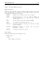
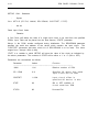
Warnings, Cautions, and Notes
as Used in this Publication
Warning
Warning notices are used in this publication to emphasize that hazardous voltages,
currents, temperatures, or other conditions that could cause personal injury exist in this
equipment or may be associated with its use.
In situations where inattention could cause either personal injury or damage to equipment,
a Warning notice is used.
Caution
Caution notices are used where equipment might be damaged if care is not taken.
Note:
Notes merely call attention to information that is especially significant to
understanding and operating the equipment.
This document is based on information available at the time of its publication. While efforts
have been made to be accurate, the information contained herein does not purport to cover all
details or variations in hardware or software, nor to provide for every possible contingency in
connection with installation, operation, or maintenance. Features may be described herein
which are not present in all hardware and software systems. GE Intelligent Platforms assumes
no obligation of notice to holders of this document with respect to changes subsequently made.
GE Intelligent Platforms makes no representation or warranty, expressed, implied, or statutory
with respect to, and assumes no responsibility for the accuracy, completeness, sufficiency, or
usefulness of the information contained herein. No warranties of merchantability or fitness for
purpose shall apply.
* indicates a trademark of GE Intelligent Platforms, Inc. and/or its affiliates. All other
trademarks are the property of their respective owners.
©Copyright 2010 GE Intelligent Platforms, Inc.
All Rights Reserved
.*.
III
PCIM User’s Manual
GFK-0074
PREFACE
The intent of this manual is to supply the user with enough information to establish the
GENIUS I/O IBM PC interface Module (PCIM) as an entry point into the GENIUS I/O
System.
The PCIM is designed to be integrated into a user-developed IBM PC
microprocessor-based system. It provides a low cost ‘tap’ on the GENIUS I/O bus,
allowing a host system to monitor and control remote I/O utilizing the extensive
diagnostics, high reliability and noise immunity of the GENIUS l/O System.
Intended
Audience
This manual is intended for design engineers and systems or applications programmers
who are already familiar with Basic or C programming in the IBM personal computer
environment. Readers are further assumed to be familiar with the GENIUS I/O System.
How to use this Manual
This manual provides a description of the GENIUS I/O IBM PC Interface Module
(PCIM), and procedures for its setup, programming, operation, and troubleshooting from a
user’s point of view. The manual should be regarded as a self-teaching tutorial if you are
unfamiliar with the PCIM. The more experienced user will access it as a reference.
DO NOT ATTEMPT INSTALLATION, OPERATION, OR PROGRAMMING OF THE PCIM
UNTIL YOU HAVE READ THE USER’S MANUAL FRONT TO BACK. Pay particular
attention to the WARNINGS and CAUTIONS interspersed throughout the text, as
ELECTRICAL HAZARDS exist which could cause PERSONAL INJURY or DEATH, or
damage to the equipment.
PCIM User’s
iv
Manual
GFK-0074
Structure of this Manual
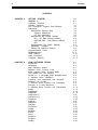
This manual contains 6 chapters and 7 appendices:
Chapter 1 - Introduction
Chapter 2 - Theory of Operation
’
Chapter 3 - Getting Started
Chapter 4 - Using PCIM - Software Drivers
Chapter 5 - Communications
Chapter 6 - Troubleshooting
Appendix A - Example
Application
Appendix B - Glossary
Appendix C - Connector Signal Descriptions
Appendix D -
Specifications
Appendix E - Part Numbers
Appendix F - Function Codes
Related Publications
The following documents in association with this manual comprise the PCIM User’s
Package:
a
GENIUS I O Bus Datagram Reference Manual -
GFK-0090
?
GENIUS I O
GEK-90486
User’s Manual -
V
Contents
GFK-0074
CONTENTS
CHAPTER
1.
CHAPTER 2.
INTRODUCTlON
Genius I/O System Overview
Genius I/O IBM PC Interface Module (PCIM)
Daughterbaard
Genius l/O IBM PC Interface Module (PCIM)
Motherboard
l-l
l-l
THEORY OF OPERATION
Introduction
PCIM Hardware Description
PCIM Motherboard Physical Structure
PCIM Daughterboard Physical Structure
PCIM Hardware Operation
Serial Interface
Data Buffer
Host Interface
PCIM Software Operation
Serial Interface
Software
Functionality
Power Up And Initialization
Steady State Operation
PCIM Manager
Software
Functionality
Power Up And lnitializat ion
Steady State Operation
Shared RAM Interface
Shared Ram Updates
Device Log In
Device Log Out
Memory
Configuration
I/O Table Lockout
Device I/O Table
Input Table
Output Table
PCIM Broadcast Control Output Table
PCIM Directed Control Input Table
Device Configuration Table
PCIM Setup Table
PCIM Status Table
Interrupt Tables
PCIM Motherboard Operation
Watchdog T imer
Power Supply Voltage Detector and Reset
Circuit
Reset Restrict ions
Host System Interrupt Control
PCIM
Electrical Characteristics
Power Supply Requirements
Bus Loads/Drive Capabi Ii ty
Signal Conditioning
2-l
2-1
2-1
2-l
2-l
2-3
2-3
2-5
2-6
2-7
2-7
2-7
2-7
2-8
2-l 0
2-l 0
2-l 0
2-l 2
2-l 4
2-14
2-14
2-l 4
2-l 4
2-l 7
2-17
2-17
2-17
2-l 8
2-18
2-18
2-18
2-l 8
2-19
2-20
2-21
l-3
1-3
2-21
2-21
2-21
2-22
2-22
2-22
2-22
Contents
Vi
GFK-0074
CONTENTS
CHAPTER 3.
GETTING STARTED
Introduct ion
Hardware Required
Software Required
Bus Termination, Jumpers, and Resistors
Addressing
Motherboard Memory Map
Segment Addressing
I/O Port Addressing
Motherboard Dip Switch Settings
SW1 - I/O Base Starting Address
SW2 and SW3 - Host Memory Address
SW4
Daughterboard Dip Switch Settings
Application
Example
Setting Dip Switches Example
Communications Cable
PCIM lnstal lation
PCIM Startup
HHM Connector
Faceplate Marking
CHAPTER 4.
PCIM SOFTWARE DRIVER
Introduction
Languages
Host Operating System
Software Driver Function Calls
Using Software Driver Function Calls
This Chapter Has Two Sections
Section A - C Language PCIM Software Driver
C Software Driver Installation
Compiling Your Application with Microsoft
Software File Linkage
C Software Driver Function Call Parameters
Summary of C Data Structures
C Software Driver Function Cal! Presentation
InitlM
ChgIMSetup
GetlMState
GetBusConf ig
GetDevConf ig
DisableOut
GetBusln
PutBusOut
GetDevln
PutDevOut
GetlMln
PutlMOut
EetCir
PutCir
GetWord
PutWord
SendMsg
3-1
3-l
3-1
3-l
3-2
3-3
3-3
3-3
3-3
3-4
3-4
3-5
3-6
3-6
3-10
3-11
3-12
3-l 3
3-14
3-l 5
3-l 5
4-t
4-l
4-1
4-l
4-1
4-3
4-3
4-4
4-4
4-4
4-4
4-5
4-5
4-l 2
4-l 3
4-16
4-l 9
4-21
4-23
4-25
4-27
4-29
4-31
4-33
4-35
4-36
4-38
4-40
4-42
4-44
4-46
Contents
vi i
GFK-0074
CONTENTS
CHAPTER 4.
PCIM SOFTWARE DRIVER (Cont’d)
SendMsg Reply
ChkMsgStat
GetMsg
Get lntr
Putlntr
Section B - Basic Language PCIM Software Driver
Basic Software Driver Installation
Basic Software Driver Function Call Parameters
Basic Data Array Structures
Error Status Indication
Access from Basic
Coding Basic Function Calls
Basic Software Driver Function Call Prsntation
InitlM
ChglMSetup
GetlMState
Get BusConf ig
Get DevConf ig
DisableOut
Get Busln
PutBusOut
EetDevln
PutDevOut
Get Hvlln
PutlMOut
GetCir
PutCir
GetWord
PutWord
SendMsg
SendMsgReply
ChkMsgStat
GetMsg
Get lntr
Putlntr
CHAPTER 5,
COMMUNICATIONS
Introduction
Types of Data
Global Data
Global Data Paths
Datagram Data
Specifying the Address for Read Device
and Write Device Datagrams
When the Datagram Target Address is
Register Memory
When the Datagram Target Address is
the Series Six PLC CPU l/O Status Tables
Response Time
Bus Scan Time
4-48
4-51
4-43
4-55
4-57
4-59
4-59
4-59
4-60
4-65
4-66
4-67
4-68
4-69
4-72
4-74
4-76
4-77
4-80
4-82
4-84
4-86
4-88
4-90
4-92
4-94
4-96
4-98
4-100
4-l 02
4-l 04
4-l 07
4-l 09
4-111
4-113
5-f
5-l
5-l
5-l
5-2
5-2
5-5
5-6
5-6
5-7
5-7
viii
Contents
GFK-0074
CONTENTS
CHAPTER 6.
TROUBLESHOOTlNG
Introduct ion
Troubleshooting Resources
Replacement Module Concept
PCIM Troubleshooting
Fault Isolation and Repair
6-l
6-I
6-2
6-2
6-3
6-3
APPENDIXES
APPENDIX
A.
B.
C.
D.
D.
E.
F.
Example Application
Glossary
Connector Signal Descriptions
Connector Signal Descriptions
Connector Pin Designat ions
Specifications
Electrical
Power Requirements
Bus Loading
Bus Drive Capability
Specifications (Cont’d)
Mechanical
Daughterboard Dimensions
Motherboard Dimensions
Environmental Requirements - Operating
Environmental Requirements - Non-Operating
Part Numbers
Function Codes
INDEX
A-l
B-l
C-l
c-1
c-3
D-l
D-l
D-l
D-l
D-l
D-l
D-l
D-l
D-2
D-2
E-l
F-l
I-1
FIGURES
Figure 1 .1
1.2
2.1
2.2
2.3
2.4
3.1
3.2
3.3
3.4
3.5
5.1
5.3
GENIUS I/O System Block Diagram
GENIUS I/O IBM PC Interface Module (PCIM)
PCIM Motherboard/Daughterboard
Layout
PCIM Hardware/Software Interface (Simplified)
PCIM Block Diagram
Shared RAM Interface Map
Jumpers JPI and JP2
Dip Switches on the PCIM Pair
Communications
Connector
PCIM lnstal lat ion
HHM Connector
Global Data Paths
PCIM Bus Time
l-2
l-3
2-2
2-4
2-13
2-15
3-2
3-4
3-12
3-13
3-14
5-3
5-8
TABLES
Table 6.1
LEDs
6-3
Introduction
l-l
GFK-0074
CHAPTER 1
INTRODUCTION
This manual provides a description of the GENIUS I/O IBM PC Interface Module
(PCIM). It includes procedures for setup, programming, operation, and troubleshooting in
conjunction with the GENlUS I/O System.
Normally, GENlUS I/O will be controlled by a PLC in machine control and fast closed
loop control applications. There are various applications, however, where systems based
on GENIUS I/O blocks will be utilized with IBM PC products.
The GENIUS l/O IBM PC interface Module (PCIM) is an entry point into the GENIUS I/O
System for the IBM PC/AT/XT family. The PCIM is a motherboard/
daughterboard, designed to be integrated into a user-developed microprocessor system.
The PClM provides a low cost ‘tap’ on the GENlUS I/O bus, allowing a host system to
Ility and noise immunity
control remote I/O uti I izing the extensive diagnostics, high relbi
of the GENIUS l/O System. Bus access is provided by the PClM Software Driver, a high
level interface between applications software you develop and the PCtM. The PCIM
Software Driver consists of easy to use macro-oriented function calls you code
appropriately in your C language or Basic language applications routines.
GENIUS l/O SYSTEM OVERVIEW
The GENWS I/O is a system of inherently distributed inputs and outputs, which consists
of:
?
GENIUS l/O Blocks AC, DC, Isolated, Analog (mounted at the point of control),
0
a Bus Controller (which serves as the interface between the GENtUS I/O
system and the Series Six PLC),
and/or
?
a PClM for interface with IBM PC ATs, XTs, or CIMSTAR I,
?
a Hand Held Monitor (the portable diagnostic and configuration tool used for
addressing, trouble-shooting, monitoring, scaling and configuring the I/O
Biocks),
0
and the GENIUS Serial Bus, which provides communications between the Bus
Controller, Hand Held Monitor, and up to 30 I/O Blocks over a single shielded
twisted wire pair.
l-2
Introduction
GFK-0074
GENIUS l/O Blocks provide superior, built-in Diagnost ics which detect open circuits,
short circuits, overloads, and a variety of other malfunctions which are beyond the power
of conventional PLCs to detect.
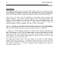
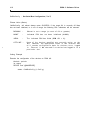
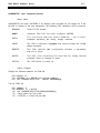
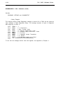
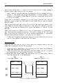
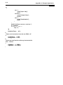
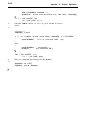
A simplified diagram of the GENIUS I/O System is shown in Figure 1.1. The PLC, CPU,
and I/O rack are standard Series Six units. The Host Controller is, for this application, an
IBM PC compatible of your choice. The GENIUS serial bus connects I/O Blocks with a
single shielded twisted pair up to 2000 feet from the Bus Controller.
a41142
SERIES SIX PLUS (
0
0
0
0
0
1GE WORKMASTER.
1-
0
0
0
0,c
I
I
SERIES SIX I/O
HAND HELD MONITOR
I- BUS CONTROLLER
I/0
BLOCKS
Figure 1.1 GENIUS I/O SYSTEM DIAGRAM
Introduction
1-3
GENIUS I/O IBM PC INTERFACE MODULE (PCIM)
Daughterboard
The GENIUS I/O IBM PC Interface Module (PCIM) daughterboard is a general purpose I/O
Controller for the GENIUS I/O System. Like the Series Six PLC Bus Controller, the PCIM
daughterboard provides a convenient method to control devices on the GENIUS serial
bus. The PCIM daughterboard performs the housekeeping tasks of initialization and fault
management for up to 30 bus devices, keeps up-to-date images of the l/O controlled by
each device (whether the device is a GENIUS t/O Block or other bus device), and can
communicate with other Controllers on the GENIUS bus by passing background messages
not associated with I/O commands. The interface to this RAM is optimized for the IBM
personal computer bus.
The network data rate is configurable by an on-board dip switch to 38.4, 76.8, or 153.6
kiiobits per second with twisted pair or twinaxial cable.
Thus, the PCIM daughterboard handles protocol and provides a general purpose, non-time
critical method of tapping in to the GENIUS twisted pair network.
Motherboard
The GENIUS I/O IBM PC Interface Module (PCIM) motherboard provides a convenient way
to interface an Open Architecture daughterboard like the PCIM daughterboard to an IBM
compatible Host system. All the signals necessary to communicate-to a daughterboard
a r e buffered through the motherboard to the Host bus. In addition to the normal
interface lines, the motherboard provides the following daughterboard control and
monitoring functions:
??
A standard ‘unit load’ to the IBM bus.
??
Low supply voltage detection.
?? Power
??
up RESET signal sequencing.
Host system address decoding over the full PC, XT or AT memory
maps.
A built-in watchdog timer (user-disabled by a jumper) that can monitor system
operation and shut down the daughterboard if the Host system faults, preventing
any conflicts on the GENIUS bus.
??
l-4
Introduction
GfK-0074
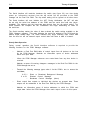
b41682
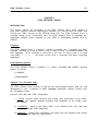
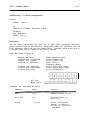
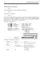
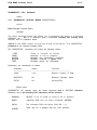
Figure 1.2 GENIUS I/O IBM PC INTERFACE MODULE (PCIM)
Theory of Operation
2-l
CHAPTER 2
THEORY OF OPERATION
INTRODUCTION
This chapter explores the physical configuration/operation of the PCIM, and provides a
description of module general capabilities. PCIM physical structure is described in the
first sect ion. PCIM hardware, functionally divided into three primary sections, is
discussed in the second section. PCIM software is functionally divided into two
subsystems; explained in the following sect ion. PCIM motherboard functions are briefly
discussed next, followed by a definition of electrical and signal requirements.
You need not be familiar with the material presented in chapter 2 in order to operate
your PCIM. If you aren’t interested in how it works, just go on to chapter 3.
PCIM
HARDWARE
DESCRIPTION
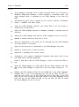
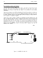
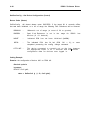
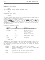
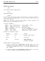
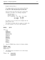
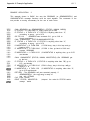
Figure 2.1 shows the PCIM Interface Module. The PCIM occupies two slots of an IBM PC
AT or XT and a single slot in a CIMSTAR I.
PCIM
Motherboard Physical Structure
The PClM motherboard is a rectangular, 2-layer board, (4.2 by 13.15 inches), with four
corner mounting holes provided. Components on the motherboard protrude no more than
.75 inches above the board surface. No components are mounted on the ‘foil’ side of the
board. Female 40 pin and a 10 pin connectors are used. Connections to the
daughterboard are made by pins from the daughterboard into the 10 and 40 pin
connectors. Connections to the Host are made by pins from the daughterboard into 36
and 64 pin edge connectors in the Host l/O rack. Figure 2.1 shows the physical
configuration of the PCIM motherboard in more detail.
PCIM
Dauqhterboard Physical Structure
The PCIM daughterboard is a rectangular, 4-layer board, (3.6 by 8.4 inches), with four
corner mounting holes provided. Components on the daughterboard protrude no more
than .75 inches above the board surface. No components are mounted on the ‘foil’ side of
the board. Two male connectors are used, a 40 pin connector and a 10 pin connector.
The 40 pin connector passes all the logic signals, while the ten pin connector passes
signals that require special handling (Le., GENIUS bus signals). The transformer and
hybrid are located near the 10 pin connector to keep on-board electrical noise to a
minimum.
Connections to the motherboard are made by pins through the daughterboard
into the I/O and 40 pin edge connectors. Figure 2.1 shows the physical configuration of
the PCIM daughterboard in more detail.
2-2
Theory of Operation
GFK-0074
a42018
a42019
JP2&
0
Oh
ooooooo~oooooooboooo#o*ooooooo
SW1 1
rRnillulo
0
5
SW2 I
mm
To
~GENIUSBUS
swspiiiiiq
To
HAND-HELD
WiTOR
SW4 jiiiiiq
0
0
F i g u r e 2.1 PCIM MOTHERBOARD/DAUGHTERBOARD
LAYOUT
Theory of Operation
2-3
GFK-0074
PCIM
HARDWARE OPERATION
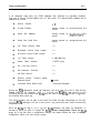
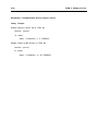
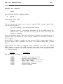
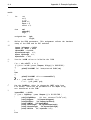
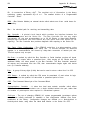
As shown in figure 2.2, PCIM hardware is functionally divided into three primary sections;
the Serial interface microprocessor (6303), the Dual Port RAM (DPR), and the PCIM
Manager microprocessor (64180).
PCIM hardware primary sections include the following components:
-
Serial lnterf ace - 6303 microprocessor, MIT chip, crystal, transmit/receive
hybrid circuit and isolation transformer.
?
Data Buffer - 20K X 8 Dual Port Shared RAM (DPR).
-
Host Interface - PCIM Manager (64180 microprocessor), 16K X 8 Shared RAM
(SRI), EPLD, buffers and transceivers.
PCIM hardware operation is discussed below.
figure 2.3.
Component interface details are shown in
Serial Interface
In the same way that the Series Six PLC Bus Controlfer serves as the communications
interface with devices on the GENIUS serial bus and the Series Six PLC, the Serial
Interface portion of the PCIM handles the details of the hardware interface to the serial
bus.
The Serial Interface microprocessor (6303) sequences the actions of the Serial Interface.
Its primary purpose is to transfer and format data between the Dual Port RAM (DPR) and
the MIT chip.
The MIT handles the details of the hardware interface to the serial bus, and in addition,
provides many support functions (such as CRC generation, error checking, a watchdog
timer function, chip selects, LED drivers and processor clock signals). The MIT receives
directed messages only if its current device number matches the device number of the
broadcast message. The device number (serial bus address) of the PCIM is transmitted
when directed messages are sent by the MIT. The device number is set in the MIT by the
Serial Interface microprocessor (6303) according to the hardware dip switch (see figure
3.2).
2-4
Theory of Operation
GFK-0074
a42016
SERIAL
BUS
1
I
I
IMERFACE
Manager
MICROPROCESSOR
I
I
I
(64180)
I
GENI
I
MANAGER
I -
l- --------- .-------
Figure
2.2
PCIM
HARDWARE/SOFTWARE
-
I
I
I
I
-1
-l
-
INTERFACE
- -I
(SIMPLIFIED)
Theory of Operation
2-5
CFK-0074
The PClM Serial Interface also includes a transmit/receive hybrid circuit and a
transformer.
Serial Interface components work together to communicate with the serial
bus and implement the following specific functions:
a
Transmit messages to the serial bus using the serial bus protocol. These
messages are written to the transmit buffers in the MIT chip by the 6303
When the MIT chip determines that it is its turn on the bus, it
microprocessor.
allows the messages in the transmit buffers to be transmitted. The hybrid
circuit translates MIT transmit and receive signals levels to levels appropriate
for transmission on the serial bus. The transformer provides isolation between
the twisted pair wires and the PC/M circuitry.
-
Receive messages from the serial bus. These messages are read from the
receive buffer in the MIT chip by the 6303 microprocessor.
-
Manage an external clock for running the 64180 microprocessor.
?
Control 2 LEDs which are used to indicate the status of the board (PCIM OK,
COMM OK, diagnostic faults).
-
Allow two chip selects - one for the 6303 microprocessor and one for accessing
the Dual Port RAM (DPR).
-
Permit a watchdog timer function for the PCIM.
Data Buffer
The Dual Port RAM (DPR) is the area where the PCIM Manager microprocessor (64180)
and the Serial Interface microprocessor (6303) exchange data. This hardware allows the
2OK Dual Port RAM to be accessed simultaneously without loss of data. The DPR, then,
is arranged to prevent conflicts when both microprocessors try to move data through the
RAM at the same time. In a manner similar to the arbitration used between the PClM
Manager and the Host Shared RAM (SRI), the Dual Port RAM is controlled by an EPLD,
which arbitrates memory requests on a byte-by-byte basis. The EPLD actually controls
the buffers and transceivers each microprocessor uses to read or write from/to the Shared
RAM. Thus, the Dual Port RAM removes any timing skews between the two processors
which are running two separate, asynchronous systems.
2-6
Theory of Operation
Host Interface
l-lost Interface hardware allows the Shared RAM Interface (SRI) to be accessed by either
the PCIM Manager microprocessor (64180) or the Host system without a loss of data. The
PCIM Manager microprocessor (64180) transfers data between the Shared RAM Interface
(SRI) and the Serial Interface microprocessor (6303) through the Dual Port RAM (DPR).
Either source can access the SRI simultaneously, byte-by-byte, without worrying about
software arbitration. The hardware arbitrates requests for the Shared RAM interface and
keeps the timing straight. As a result, the SRI looks like a pure RAM device to both
systems. If the Host requires that more than one byte of data be transferred without any
intermediate byte accesses from the PCIM, a software lockout scheme is used. The
interface signals are directly compatible with those of the PC backplane.
The PCIM Manager microprocessor (64180) sequences the actions of the PCIM Manager,
whose primary purpose is to transfer and format data between the Shared RAM Interface
(SRI) and Dual Port RAM (DPR) by executing a program located in the EPROM.
In addition, the PCIM Manager generates an interrupt when important information has
been deposited into the SRI. When the Host desires to write or read grouped multi-byte
data, it can request a lock out of the Shared RAM. The Host initiates this lock out by
writing the request in the Command byte of the SRI, which causes an interrupt for the
PCIM Manager. The PCIM Manager acknowledges the interrupt by setting a bit in the SRI
and pulsing the interrupt line to the Host.
The Shared RAM interface (SRI) is the user’s interface to the PCIM. An EPLD arbitrates
Shared RAM memory requests on a byte-by-byte basis and allows the Host and PCIM
Manager equal simultaneous access to any byte of Shared RAM without loss of data. The
SRI contains 16K bytes for I/O tables, configuration data, diagnostic data, labels and
background message queues.
Theory of Operation
2-7
GFK-0074
PCIM SOFTWARE O p e r a t i o n
PCIM software is functionally divided into two subsystems:
-
Serial
?
PCIM Manager software.
Interface
software.
The Serial interface software provides the interface to the GENIUS serial bus from the
Dual Port RAM (DPR), the shared RAM area between the Serial Interface and the PCIM
Manager. PCIM Manager software primarily interfaces and formats data from the Dual
Port RAM area into the Shared RAM Interface (SRI), the shared RAM area between the
PCIM Manager and the Host system.
Serial
Interface
The primary responsibility of the the Serial Interface portion of PCIM software is
GENIUS l/O Network Protocol. The Serial Interface handles keeping the PCIM active on
the GENIUS serial bus. Since the PCIM is a control device, it must be able to receive
control data from all devices on the bus and must be able to direct control data to any
given station on the bus.
The secondary function of the Serial interface software is to maintain the overall
operation of the PCIM. This is accomplished by servicing the MIT watchdog timer and
maintaining a ‘heartbeat’ with the PCIM Manager. If any of these fail, then the Serial
Interface generates a reset signal and the PCIM becomes inactive.
Serial
Interface
Software
Functionality
Power Up and Initialization
When power is applied to the PCIM, the Serial Interface begins performing power up
initialization. The following set of circuitry/hardware power up diagnostic tests are run:
?
EPROM Checksum Test
-
Microprocessor Self Check Test
-
MIT Bus lest
-
RAM Test
If any of the tests fail, the software attempts to go into a controlled lock-up state
preventing the PCIM from running at all. If the diagnostics pass, the Serial Interface
completes initialization of its memory variables, Dual Port RAM, the MIT and other
hardware or software related variables necessary to begin steady state operation.
Theory of Operation
2-8
GFK-0074
The Serial Interface will read--the hardware dip switch (see figure 3.2) one time during
power up. Information received from the dip switch will be provided to the PCIM
manager via the Dual Port RAM. The dip switch setting will be ignored at all other times.
The Serial Interface will next initialize the MIT. During initialization, the MIT will also
be set with the serial bus address of the PCIM and the serial bus baud rate (when
available). The address and the baud rate are derived from the dip switch setting. The
Serial Interface will complete the MIT initialization and begin transmitting its token on
the serial bus.
The Serial Interface makes the value of the on-board dip switch setting available to the
PCIM Manager software. This value indicates the serial bus address of the PCIM and the
default output disable flags. The Serial Interface may begin collecting input control data
from the bus but will not transmit output control data until there is data to transmit.
Steady State Operation
During normal operation, the Serial Interface software is required to provide the
following functions for the PCIM Manager software:
?
Maintain a Dual Port RAM table of control inputs from all devices on the bus
for the PCIM Manager. Maintain an information queue of device addresses
which sent input data.
-
Inform the PCIM Manager whenever new control data from any bus device is
received.
-
Maintain a queue of incoming datagram messages in the Dual Port RAM for the
PCIM Manager to act on.
-
Transmit the following message types when it is the PCIM’s
,
serial bus;
0 Of 1
0 to 31
1
turn to access the
Direct or Broadcast Background Message
Directed Control Message
Broadcast Control Message (token)
?
Direct control data outputs to individual bus devices as grouped data. These
outputs will be maintained in the Dual Port RAM by the PCIM Manager.
-
Maintain an information queue of device addresses to which the PCIM sent
output data. Inform the PCIM Manager when each output is sent via this queue.
Theory of Operation
2-9
Send datagram messages from a single message buffer as a Directed or
Broadcast Background Message in either restricted or unrestricted mode. This
single message buffer is maintained by the PCIM Manager in the Dual Port
RAM.
Reinitialize the MIT chip to support the two priority classes of Datagram
Service - NORMAL and HIGH Priority.
Inform the PClM Manager whenever new control data for all bus devices is
received from the serial bus.
Inform the PCIM Manager whenever a datagram message is received from the
serial bus.
Interrupt the PCIM Manager each time the PCIM completes its turn on the bus.
Maintain a minimum serial bus scan time of 3 ms.
Stop any transmission on the serial bus on command from the PCIM Manager
for a time period of 1.5 seconds.
Report the bus scan time in milliseconds to the PCIM Manager every scan.
Maintain a running count of serial bus errors.
Implement a watchdog timer service routine.
Continuously run a series of background diagnostic tests which verify its own
local RAM and its EPROM (checksum).
Detect a fatal failure with the PCIM Manager in order to cause the PCIM to
halt.
Inform the PCIM Manager of a fatal failure with the Serial Interface, and allow
to
time for the PCIM Manager to report this to the host before causing the
halt.
Maintain the LED indicators PCIM OK and COMM OK. If the PCIM Manager’s
heartbeat fails or any of the diagnostics fail, turn off the PCIM OK LED. If a
serial bus error occurs, turn off the COMM OK LED for 200 msec. If the PCIM
does not get a turn on the bus within the allotted time period dependant on the
baud rate, turn off the COMM OK LED. In this last case, the LED will remain
IM gets its turn on the bus.
off until the PC
2-10
Theory of Operation
GFK-0074
PCIM Manager
The basic function of the PCIM Manager is to provide data flow between the serial bus
and the Host via a formatted shared RAM interface. Key functions of the PCIM Manager
include:
?
transfer of sampled data (I/O or Global Data Services) to and from other
devices on the bus. This data is for basic I/O devices, or global data which is
shared between other types of devices such as processors
-
transfer of unique data (Datagram Service) to and from other bus devices, This
data includes configuration, diagnostic and other types of unique data
-
maintenance of device characteristics in a Configuration Table
device, PCIM, bus and syntax error reporting
PCIM Manager Software Functionality
Power Up and Initialization
When the Host is ready to use the PClM function, it allows the PCIM to be reset. The
Serial Interface then begins its power up sequence. Again, when the Serial Interface
completes its power up and diagnostics, the PClM Manager can begin operation.
During power up, the PClM Manager performs diagnostic tests on all of its related
hardware. These tests include:
-
EPROM Checksum Test
?
Microprocessor Test
-
RAM Test
If an error is found in any of the diagnostics, the PCIM Manager reports the fault to the
Host through the PCIM Status, then attempts to halt. The host will not be given a PClM
OK status, nor will the PCIM OK LED Ilight.
Theory of Operation
2-11
GFK-0074
If all diagnostic tests pass, the PCIM Manager then initializes its operating variables.
The Loss of Device Timeout will be set to 3 bus scans. The Shared RAM variables will be
defaulted as fol lows:
Device
=o
Present
Output Disable
setting based on daughterboard dip
switch
Serial
setting based on .daughterboard
switch
Bus
Address
dip
Serial Bus Baud Rate
setting based on daughterboard dip
switch
l/O
= o
Table
Broadcast
Lockout
Control
State
Data
Length
= o
Directed Control Data Length
= o
I/O Table Length
= 128 (80 hex)
Status
= OFFFF (hex)
Table
Address
All interrupt Status
= o
All interrupt
= o
Disable
= o
All PCIM S t a t u s
Receive Queue,
Request Queue
Transmit
Command Block Status Byte
During the PCIM
Shared RAM for
indicating self-test
two seconds after
Buffer,
= empty
= Command Complete
Manager’s power up sequence, the Host must not read or write to the
1.7 seconds. After 1.7 seconds, the PCIM OK flag should be ON
has passed (the PCIM sets the state of the PCIM OK byte to ‘1’ within
power up).
The Serial Interface will not write to the Dual Port RAM or begin transmitting on the bus
until the PCtM Manager informs it that power u p processing has been successfully
completed.
Once the PCIM OK flag is set to ‘I’, the PCIM Manager will delay an additional 1.5
seconds to allow the Host to change the PCIM default configuration. Since the PCIM
drops off of the bus after a configuration change, this feature allows the host to change
configuration before any bus activity begins.
2-l 2
Theory of Operation
GFK-0074
Steady
State
Operation
From this point, the PCIM Manager runs in steady state operation. Operation of the
PCIM Manager is closely related to that of the Shared RAM Interface, including;
Self -Test - During steady state operation, the PCIM Manager is required to perform
background diagnost ics. These tests include a non-destructive private RAM test, a
checksum of the EPROM, and maintainenance of a heartbeat with the Serial Interface. If
any faults are found in these background diagnostics, the PCIM Manager reports the fault
through the PCIM Status area of the Shared RAM, disable outputs to the serial bus, and
then attempt to halt all processing.
I/O Table Lockout - To ensure data coherency for all control data to and from the Host,
the PCIM Manager will implement a ‘lockout’ of all control data tables during an I/O
Lockout Request. During I/O Table Lockout, the PCIM Manager will NOT access the
Input Tables, the Output Tables, the Broadcast Control Output Table and the Directed
Control input Table.
Host Interrupts - There are seven conditions requiring immediate Host attention which
causes the PCIM Manager to interrupt the Host. Before interrupting the Host, the PCIM
Manager will set the interrupt condition in the Interrupt Status Table of the SRI by
The i-lost w i II clear the
writing a ‘1’ to the byte indicating the interrupt condition.
Interrupt Status Table entry when it has completed servicing that interrupt.
The Host may disable any of the seven interrupt conditions via the Interrupt Disable
Table. When the PCIM Manager determines that one of the interrupt condition exists,
that byte in the Interrupt Status Table is set. Then, the Interrupt Disable Table will be
interrogated.
If the corresponding disable flag is set, no interrupt will be generated to
the HOST. The HOST will still be responsible for clearing the corresponding byte in the
Interrupt Status Table (see chapter 4).
Whenever control data is received, the PCIM Manager will determine if that particular
device is already ‘logged’ into the Configuration Table. If so, the PCIM Manager accepts
the control data and places it into the Input Table. If not, the PCIM Manager requests
control data parameters from that device. The control data is ignored until these
parameters are received by the PCIM Manager.
2-13
Theory of Operation
.-. .~
GFK-0074
Figure 2.3 shows the interrelationships among the various lines and components.
b42020
,
XSCVR 1
A
cDEi;DR
KKK8 <
SRAU
3
BUFFER
II
IOPIpi CONNECTOR
1 1
Ep
ZS
;it!II
2n d #
: I 8PI
+%
Q=L
SELECT
It
+
DlP
swmHEs
GENIUSBUS
CONNECTORS
,
I
1
,
I
MDRESS .
WYPARATDR
COlltinEYtTDR
I
l/U SELECT
?
LINE PROTECT
I
i
I
IBM BACKPLANE CONNECTOR
Figure2.3 PCIM BLOCK DIAGRAM
V
XSCVR
Theory of Operation
2-l 4
SHARED
RAM
INTERFACE
As you remember, all data passed between the Host system and the. PCIM goes through
Host shared RAM, referred to as the Shared RAM Interface (SRI). As stated, this RAM
looks like an 16Kx8 static memory device to the Host system. Although all areas of RAM
are ‘read/write’, that is, fully accessible by the Host to read or write to any RAM
location, some areas of the RAM are not accessed by the Software Driver during normal
operation (as shown in figure 2.4).
Shared RAM Updates
Some data is transferred between the Shared RAM and the serial bus automatically by the
PCIM manager. This type of communication includes I/O circuit updates, fault reports,
and the like. The rest of the calls and message types must be initiated by the Host
system using the Software Driver, explained in more detail in chapter 4.
Device tog In
The PCIM Manager will log in a device whenever control data is received from a device
that is NOT listed in the Host’s SRI. A device is considered logged in, or on-line, when
the PCIM Manager has that device’s configuration data translated and stored in the SRI (a
GetBusConfig call can be used to verify the presence of the device on the bus). At this
point, the device is considered logged in and input control data from that device will be
transferred to the SRI Input Table.
Heavy log in activity occurs after power up of the PCIM Manager if there are no devices
logged in the SRI. Once in steady state, Jog in activity occurs whenever Broadcast
Control data is received from a device that has just been included on the serial bus.
You may want to code the InitlM call (see chapter 4) in your program logic first (in order
to allow devices on the bus to log in with the PCIM), and then perform the rest of your
program logic initializations in order to optimize front-end timing.
Device Log Out
The PClM Manager will log a device out whenever Broadcast Control data is not received
for three (3) consecutive serial bus scans. This timeout period is fixed by the PCIM
Manager. When Device Log Out occurs, the PCIM Manager will not direct output data to
that device from the Serial Interface, and will inform the Host of the Loss of Device.
The device remains logged off until the PCIM Manager receives identification data from
it. When new Broadcast Control data is received from any device which is not logged in,
the PCIM Manager will begin its device log in procedure.
Memory
Configuration
Following is the memory map for the PCIM 16K Shared RAM Interface. It shows the
different areas used to convey data, status, control and diagnostic information to and
from the Host system. A complete map of the Shared RAM Interface is shown in figure
2.4.
2-15
Theory of Operation
GFK-0074
Request Queue
16 X 136
Serial Bus access
to Host memory
(2176)
Request Queue *
Head Pointer
(1)
Pointer to buffer
t-lost is reading
Request Queue
Tail Pointer
Pointer to buffer
PCIM i s w r i t i n g
(1)
PCIM and Serial Bus
Characteristics
PCIM Setup
Table
(16)
PCIM and Serial Bus
Diagnostics
PCIM Status
Table
(16)
interrupt Status
Table
(16)
Host
Interrupt Disable
Table
(16)
Disable
Host Interrupts
Command B lock
D r i v e r Calls t o
PCtM Manager
*
interrupts
(16)
Output Data Area
Transmit Datagram
Buffer RAM
(240)
* Host write to these locations causes Interrupt to the PCIM Manager
figure 2.4 Shared RAM Interface Map
Theory of Operation
2-f 6
GFK-0074
Input Data Area
Read Datagram
Buffer RAM
(134)
I/O Table Lockout *
Request/Relinquish
(1)
I/O
Table Lockout
State
(1)
Host interrupt
Clear
PCIM Lockout of
the I/O Tables
Lockout State
according to PCIM
Byte to Clear the
Host Interrupt
(1)
Reserved RAM
Reserved RAM
(5045)
Device Configuration
Table
32 x 8
(256)
Device ID, status
and setup
Di rected Input
t o PCIM
Directed Control
Input Table
(128)
Broadcast Control
Output Table
Broadcast Output
from PCIM
(128)
Device
- - Input/Output
Tables
- -
Device Inputs
and Outputs
to/from the
serial bus
* Host write to these locations causes Interrupt to PCIM Manager
Figure 2.4 Shared RAM Interface Map (Cont’d).
Theory of Operation
2-l 7
GFK-0074
I/O Table Lockout
To ensure data coherency for all control data to and from the Host, the PCN Manager
will implement a ‘lockout’ of all control data tables during an I/O Lockout Request. This
feature prevents the PClM Manager from accessing the SRI at the same time that the
Host is updating it. Two bytes in the Shared RAM Interface (SRI) are dedicated to the
I/O Lockout feature: I/O lockout Request/Relinquish, and t/O Table Lockout State.
The maximum response time to the t/O Table Lockout Request will be determined by the
time required for the PCIM Manager to transfer 128 bytes to or from the Input or Output
Table. Normally, the response will be less than this time. However, if the PCIM Manager
is currently transferring data to or from the Input or Output Table, it will complete the
current data transfer before accepting and enabling the lockout. When the Host has
completed its control data access, the PCIM Manager will resume normal operation in
servicing control data to and from the SRI.
Device I/O Table
The Device l/O Table resides in the last 8K bytes of the Shared RAM memory and is
divided into two tables - the Device Input Table, and the Device Output Table (see
chapter 5). The Input Table wili contain the Broadcast Control Data from each logged in
device. The input Table is updated every serial bus scan unless I/O Lockout is enabled.
Data placed in the Output Table by the Host will be sent to each logged in device every
serial bus scan.
Both the Input and Output Tables are organized in groups of up to 32 segments each
(corresponding to the maximum possible number of devices on the bus). Segment lengths
are fixed at 128 bytes.
Jnput Table
All Broadcast Controt
with that particular
segment 12. As such,
be able to determine
Data will be placed in the Input Table in the segment associated
device. That is, control data from device #I2 will be placed in
the Input Table can be thought of as an array table. The Host will
the type of I/O Block from the Device Configuration Table.
Output Table
The PClM Manager will take the data
the device associated with the given
control data to I/O Block #l2, it must
As with the Input Table, the format of
call.
placed in the Output Table and direct that data to
Output Table segment. If the Host wants to send
place that data in segment 12 of the Output Table.
each individual segment is established in the lnitlM
2-1 8
PCIM
Theory of Operation
Broadcast Control Output Table
The PCIM Manager will transmit its own Broadcast Control Data onto the serial bus once
per scan. The Host will place data in the Broadcast Control Output Table for the PCIM
Manager to broadcast (see chapter 5).
PCIM Directed Control Input Table
The PCIM Manager may receive Directed Control Data from any device capable of
sending this type of message to the PCIM. The Directed Control Input Table is provided
in the SRI for this data (see chapter 5).
Thus, a series of Hosts may be placed on a single bus and communicate with each other.
Using the Broadcast Control Output Table, all PCIMs can broadcast control data to all
other PClMs on that serial bus. Using the Directed Control input Table, a single PCIM
can be controlled by another PCIM. This a powerful feature of the PCIM Manager.
Device Configuration Table
The Device Configuration Table, 256 bytes long, contains the device ID, status, setup and
other characteristics of each device connected to the serial bus controlled by this PCIM.
Parameters are received by the PCIM Manager via an InitlM or ChglMSetup call. These
tables are formatted into 32 segments of 8 bytes per segment. One 8 byte segment is
reserved for each of the 32 possible devices, with the lowest, device number 0, residing in
the first 8 byte segment.
PCIM Setup Table
The PCIM Setup Table contains parameters unique to a particular PCIM. These
parameters consist of device related values. When the Host changes one or more of these
parameters, the PCIM Manager will log all devices out of the database and drop all bus
transmissions for 1.5 seconds, the time period necessary to cause all receiving devices to
log out the PCIM. When the PCIM begins re-transmitting, these devices will re-log in to
the PCIM with the new parameters.
PCIM Status Table
The PCIM Status Table contains six bytes indicating the veracity of the PCIM software
and the status of the PCIM hardware. When certain status bits change, the PCIM
Manager will set the PCIM Status Change byte in the Interrupt Status Table. If this
interrupt is not disabled, the PCIM Manager also will cause a Host interrupt to occur.
interrupt Status will be set when for a RAM fault, an EPROM fault, or for excessive bus
errors.
Theory of Operation
2-19
GFK-0074
Interrupt Tables
Several conditions occur which can cause the PCIM Manager to set a byte in the Interrupt
Status Table, and possibly result in the generation of an interrupt for the Host. The
following is an explanation of each condition:
-
Interrupt Summary Status - Whenever the PClM Manager causes an interrupt to
the Host, the interrupt Summary Status byte will be set in the Interrupt Status
Table. If this byte is set in the Interrupt Disable Table, the PCIM Manager will
not interrupt the Host for any reason.
?
Request Queue Entry - Certain messages received from devices on the bus will
be separated out from all other messages and placed in the Request Queue.
The PCIM Manager will then set the Request Queue Entry byte.
-
PCIM Status Change - When certain items within the PCIM Status Table
change, the PCIM Manager will indicate this change by setting the PClM Status
Change byte.
-
Device Status Change - Anytime that a device on the bus is logged in, logged
out or changes its configuration data, the PCIM Manager will set the Device
Status Change byte.
-
Outputs Sent - This status byte is set whenever the PCIM relinquishes its
access to the serial bus. This interrupt status can be used to synchronize to the
serial bus scan if required.
-
Command Complete - Each time the Host initiates a command, and the PCIM
Manager completes that command (with or without errors), this status byte will
be set.
-
Receive Queue Not Empty - Whenever any message is received from a device
on the serial bus that is not part of Request Queue Entry, Serial Bus Requests,
or a response from the command Transmit with Reply, this status byte will be
set. Since these messages will be queued, the Host may retrieve them via the
Read Datagram Command.
-
I/O Table Lockout Grant - When the Host requests an l/O Table Lockout (not a
Relinquish), this byte will be set to indicate when the PClM Manager is able to
enforce the lockout. The lockout is not enforced until this byte is returned to
the Host.
Theory of Operation
2-20
GFK-0074
PCIM
MOTHERBOARD OPERATION
The PCIM motherboard’s primary function is to provide an electrical interface between
the PCIM daughterboard and a Host system. The PCIM motherboard has no ‘smart’
components and therefore will be functionally transparent to the user. The motherboard
does, however, provide support features that enhance daughterboard functions and allows
the PCIM to function as an IBM PC type I/O board.
The PCIM motherboard includes the following components:
a
Address buffers
-
Data
-
Address decoders
?
PAL logic control
-
Programmable
a
Watchdog
a
Power supply control
a
Host interrupt control
?
Signal
transceiver
Peripheral
interface
timer
conditioning
Pertinent PCIM motherboard hardware operation is discussed below. Component
interface details are shown in figure 2.3.
Theory of Operation
2-21
GFK-0074
Watchdog Timer
The watchdog timer is a hardware timer that can be periodically reset and is used to
reset the motherboard. if the watchdog timer is enabled by jumper JP2 (see figure 3.1),
it must be reset periodically or it will put the PClM into RESET. You can toggle the
watchdog timer and use it as a failsafe timer to ensure that if the Host system ‘hangs up’,
the PCIM will not send any erroneous messages to the serial bus. If the watchdog timer is
disabled by JP2, you do not have to toggle it; it will stay turned off and will not put the
PCIM into RESET.
Power Supply Voltage Detector And RESET Circuit
In addition to the watchdog timer, the power supply voltage detector can put the PCIM
into RESET if it detects a low power supply voltage.
The RESET circuit monitors the system reset signal on the Host bus (called RESETDRV
on an IBM type bus), as well as the output of the voltage detector and the watchdog timer.
Reset
Restrictions
Do not enable interrupts, or read/write to the PCIM for 1.7 seconds (the period of time
required for hardware/software initialization) after reset. One false interrupt occurs
within this time period. Reading or writing to the PCIM during this time may cause the
watchdog timer to time out. The PCIM OK flag wilt be invalid during this period of time.
Host System Interrupt Control
The motherboard provides a method to interrupt the daughterboard and receive and route
an interrupt request from the daughterboard to the Host system. The Host, using the
motherboard, can interrupt the daughterboard by toggling the output line.
The daughterboard can also request an interrupt from the Host. The motherboard latches
the edge of the interrupt where it can be read or routed through a selector switch (see
figure 2.3) to one of five interrupt request lines on the Host bus. The motherboard can
reset the latch, readying it for the next interrupt.
2-22
Theory of Operation
GFK-0074
PClM Electrical Characteristics
Power
Supply
Requirements
The PCIM requires a 5 volt DC source for logic power. Supply voltage should not vary
more than 10% above or below nominal (below 4.5 V DC or above 5.5 V DC), or the PCIM
will not function correctly. The PCIM typically draws 180 milliamperes at 5.0 volts (2
10%).
Bus Loads/Drive Capability
All input lines to the PCIM present no more than one standard LSTTL load to the Host
interface connector.
All output lines from the PCIM are capable of driving 10 standard LSTTL loads. These
lines, with the exception of the /lNT and /PCIM OK lines, are tri-state outputs. The /lNT
line is an open-collector output that can be wired-ORed to a single interrupt input. The
/PCIM OK and /COMM OK lines are low-true open collector type outputs with built-in
current limiting to IO ma suitable for driving LEDs directly.
All input signals to the PCIM from the Host system look like one LSTTL load to the Host
system. These signals are TTL compatible and switch at TTL levels.
The control output signals to the Host system are open-collector LSTTL drivers with IOK
resistive pull-ups, capable of sinking 4 mA while maintaining an output voltage of 0.4V or
lower.
The data transceiver is a tri-state LSTTL device capable
with VOL = 0.4V and VOH = 2.OV.
Signal
of sourcing or sinking 12 mA
Conditioning
The PCIM has two connectors that you can access when the PCIM is installed in a PC
type rack. One of the connectors, a six-pin terminal block, is for the standard twisted
pair connection to the serial bus. The other connector, a nine-pin ‘D’ connector, is for
the Hand-Held Monitor interconnect (see figure 3.3). A 150 ohm termination resistor is
provided across the twisted pair bus to terminate the line by connecting jumper JPl.
All of the lines in from both connectors are either isolated or impedance limited to
protect the PCIM from voltage spikes or the misapplication of high voltages on the serial
bus connections.
The low-level (logic) signals are brought out on the 40 pin connector and the high level
signals (analog) are on the IO pin connector. Signal conditioning is discussed in detail in
the next chapter.
Getting
Started
3-l
GFK-0074
CHAPTER 3
GETTING STARTED
INTRODUCTION
In order for you to interface the PCIM with the GENIUS serial bus, you must first
perform the following steps:
?
Correctly terminate the serial bus.
-
Set the appropriate P
-
Set PCIM dip switches SW1 through SW5
?
Install the PCIM in the host.
?
Make a cable for serial bus communications and install this cable from the
PCIM to the serial bus.
Cjumpers.
I
M
Hardware Reauired
In addition to the devices normally considered part of the GENIUS l/O system, the
following hardware is required to effect a GENIUS l/O - PCIM - l-lost communications
interface:
-
a Workmaster, Cimstar I, IBM-AT, IBM-XT, or IBM-Clone
-
a PCIM
Software Required
The following software is required to effect GENIUS I/O - PCIM - Host communications:
?
MS DOS 3.0 or higher
-
pcim.lib (C Software Driver - small memory model)/
?
Ipcim.lib (C Software Driver - large memory model)
-
pcim.h (C Software Driver - include file)
-
pcimx.exe
-
pcim.bas (BASIC startup sequence)
and
(BASIC
Software
Driver)
All of the files above (except MS DOS 3.0) reside on the diskette you received with this
manua I.
3-2
Getting
Started
GFK-0074
Bus Termination, Jumpers, and Resistors
You must install a terminating resistor across Serial 1 and Serial 2 at both ends of each
serial bus. The value of the resistors you install will be 75, 100, 120, or 150 ohms,
depending upon the type of cable used (see chapter 2 of the GENIUS I/O User’s Manual,
GEK-90486).
There are two jumpers on the PCIM motherboard: JPl and JP2 (see figure 3.1). When the
PCIM is placed at one end of the bus, the 150-ohm terminating resistor built into it can
be used to terminate this end of the cable (when cables requiring a 150-ohm termination
are used). Install this resistor by moving jumper JPI to the l-2 posit ion. When JPl is in
the 2-3 position, no resistance is applied.
Jumper JP2 is used to enable or disable the motherboard on-board watchdog timer. This
timer is provided for users who want to monitor the Host system and shut off the PCIM
when the Host malfunctions. The timer is enabled when JP2 is in the 2-3 position. Y OU
must then pulse the timer input every 727 ms or the motherboard will reset the
daughterboard. With JP2 in the f-2 position, the watchdog timer is disabled and needs no
input from the Host system. The other portions of the RESET circuit, the voltage
detection and Host RESERDRV monitor, still provide RESET capability, even with the
watchdog timer disabled.
a4202 1
/-WATCHOOG
321 N
JP2 &I o
Ob
Monitor
150 OHM TERMINATOR
ooooooobooooooobooooooobooooooo
Figure 3.1 JUMPERS JP1 AND JP2
Getting
3-3
Started
GFK-0074
ADDRESSING
Initial setup of the PClM is easy; first set the I/O and t-lost memory addresses on the
motherboard. Then, set the PClM Serial Bus Address, Baud Rate, and output default on
the daughterboard. Finally, begin using the IM through your applications program. The
following sections show the setup procedures and provide a step-by-step example.
Motherboard Memory Map
Segment
Addressing
The memory map for the motherboard consists of four consecutive bytes of I/O space.
16K bytes of memory space suffice for the daughterboard. These I/O and m e m o r y
locations should be mapped into a ‘reserved’ area in the Host system where no memory or
device addresses reside. The dip switch settings on the motherboard (see figure 3.2)
determine the exact absolute memory locations required by the PCIM. SW1 - SW4
switches are all set OPEN from the factory.
As an example, commonly used locations are:
Segments - CC00 hex (daughterboard) I/O Addresses - 3E0 hex (motherboard)
3E4 hex
DO00 hex
I/O Port Addressing
The four bytes of mapped I/O memory space are used by the Programmable Peripheral
Interface (PPI) on the motherboard. The PPI chip consists of a microprocessor interface
and three 8-line programmable I/O ports. l/O ports are configured as input or output,
depending on the values put in the four program bytes of the PPI. The l/O base address
for the four bytes is determined by the dip switch settings described in the next section.
a42022
321
JPZ m
SW1
pimiq
SW2
SW3 ImiBl
SW4 pq
0
1
1
OOOOQOO~OOOOOOO~OOOOOOO~OQQOOOO
JPl
VOADDRESS
il
0
:
0
0
HOSThhEtKRY ADDH3S
x
0
A
3 NOT USED (ALL OPEN)
0
0
0
-1-----------???? SPECLAL BUS ADDRESS
;
?
? ?? BAUDRATE
?? OUTPUTS DISABLE
----------m-w- 0
i-l
L
Figure 3.2 DIP SWITCHES ON THE PCIM
Getting Started
3-4
GFK-0074
Motherboard Dip Switch Settings
SW1 - I/O Base Starting Address
The PPI-occupied 4 bytes of I/O space in the Host system is determined by the settings of
dip switch SW1. The starting address of the 4 byte I/O space is calculated as follows:
Dip Switch SW1
position
- - >I2345678
I
I
I
I
I
I
I
I
--> A0 Al A2 A3 A4 A5 A6 A7 A8 A9
H o s t +-’
3rd
digit
bus
address
‘-+‘T’
2nd
1st
digit
digit (notice that address is reversed)
The i/O addresses available for the motherboard must begin on 4 byte boundaries. That
is, the third digit of the I/O address must end in a ‘O’, ‘4’, ‘8’, or ‘C’ (hex). Therefore, the
starting addresses of the 4 byte I/O space range from 0 to 3FC (hex). To determine the
switch settings for a particular address, first establish the starting address of the 4 byte
I/O space in l/O memory that the motherboard should use. Convert this address value to
binary and from the figure above, set OPEN the switches on SW1 corresponding to the ‘1’
values in the binary value.
Example:
set dip switch SW1 for l/O address 3E0 (hex), first convert 3E0 to binary,
which is
TO
A0Al
I
0 0
AZA3A4A5
I
0 0 0 1
‘--I--~
0
A6A7A8A9
Illf IIll
1 1 1 1
‘-I-/
E
\?I
3
for every occurrence of a 1, set the corresponding dip switch position of SW1
OPEN as follows:
A2 A3 A4 A5 A6 A7 A8 A9
1 I I I I I I I
0 0 0 1 1 1 1 1
I I I I I I I I
Getting Started
3-5
GFK-0074
Reading and writing to the assigned I/O address provides data interchange between your
programs and the PCIM.
SW2 and SW3 - Host Memory Address
As stated, the daughterboard uses up to 16K bytes of system memory. This block of
memory is used to store I/O data, buffers for communication data, and a variety of other
information the PCIM uses. Dip switches SW2 and SW3 determine where this 16K
memory should reside. Address lines A0 through Al3 are passed on from the t-lost bus to
the PCIM connector and are not used in the address decoding on the motherboard. These
14 address lines are necessary to decode addresses in the 16K shared RAM memory on the
daughterboard.
SW2
/
1
I
2
I
3
I
SW3
4
I
5
I
6
I
\/
1
2
\
3
I
4
I
5
I
6
I
AO..ll Al2 Al3 Al4 Al5 Al6 Al7 A78 Al9
A20 A21 A22 A23
\
/\
/
I;/ ‘7’ ’
TI
4,5,6th d i g i t s
3rd digit
2nd digit (Type N/A
1st D i g i t
(Address for PC)
(High Address of
(High Address
AT/PC)
for AT)
for PC)
-
You can position this 16K shared RAM anywhere in PC, XT or AT memory using dip
switches SW2 and SW3. Six switches on SW2 and four switches on SW3 decode the ten
address lines needed to uniquely place the 16K bytes in a 16,777,216 byte memory map.
An extra switch, switch position 1 on SW3, will enable or disable the decoding of the four
high address lines A20 through A23. If the PCIM is to be used in a PC, XT, or other
system without the address capability of the AT (24 address lines), SW3 switch 1 should be
OPEN. If SW3 switch 1 is OPEN, the other switches on SW3 are ignored and can be left in
any posit ion. If your system has 24 address lines and you want to address the PCIM at an
address greater than 1M, SW3 switch l should be CLOSED. Currently, MS/PC DOS does
not support addresses greater than 1M. The example below shows dip switches SW2 and
SW3 set for segment value CC00 hex for a PC type Host.
3-6
Getting Started
GFK-0074
The memory address space in the Host memory map must start on 16K byte boundaries.
That is, the fourth, fifth, and sixth digits in the hex address of the start of the memory
address space must be zero. The third digit must always be a ‘O’, ‘4’, ‘8’, or ‘C’ (hex). So
valid memory addresses for the start of the block could be F 4 C 0 0 0 288000, 0E0000, etc.
In a manner similar to that used in l/O address decoding, dip switches SW2 and SW3 are
set up to decode the desired memory address. Switches should be OPEN to correspond to
a ‘1’ in the desired address. Remember, switch 1 of SW3 shoutd be CLOSED for addresses
greater than 1M and OPEN for addresses less then IM. Some example setups are shown
below:
SW3
Addresses
f-4cooo
288000
OEOOOO
cc000
EOOOO
‘+b
SW2
I
/
1
2
3
\
6
/
1
2
3
4
c
c
c
o
o
x
x
x
x
x
o o o o
c o c c
c c c c
x x x x
x x x x
o
c
c
o
c
o
o
c
o
c
c
c
c
c
c
c o c
c c o
0 0 0
c o o
0 0 0
4
5
C = CLOSED
0 = OPEN
5
\
6
X = Don’t Care
SW4
Switch 4 on the motherboard is the switch which controls interrupts. It determines which
IRQ level appears in the PC. If the switch is closed, IRQ value is active.
/
1
IRQ
I
2
\
2
I
6
3
I
5
4
I
4
5
6
II’
3
X
Dauqhterboard Dip Switch Settings
A single bank of Dip Switches is located on the daughterboard (as shown). These dip
switches are used to set the Serial Bus Address of the PCIM, set the Serial Bus Baud
Rate, and determine the default setting for Outputs (Enable or Disable). From the
factory, the PCIM Serial Bus Address is set to 31 (IF hex/11111 binary), Baud Rate to
153.6 standard, and Outputs are Disabled.
See the GENIUS I/O User’s Manual
(GEK-90486) for more information about the significance of these defaults.
NOTE
The PCIM Baud Rate should be set to 153.6 Standard when connected to a bus on
which Phase A devices are used. See Appendix E for a list of Phase A devices.
Getting Started
3-7
GFK-0074
yyy?zz Bus Ad res
i ---i---------------Serial Bus Baud Rate
00
01
10
11
t------------------------
- 153.6 Extended (8
- 38.4 (8 bit skip
- 76.8 (8 bit skip
- 153.6 Standard (4
bit skip time)
time)
time)
bit skip time)
Default Output Disable
0 - Outputs Enabled
1 - Outputs Disabled
The four bytes of mapped I/O memory space are used by the Programmable Peripheral
Interface (PPI) on the motherboard. The PPI chip consists of a microprocessor interface
and three 8-line programmable I/O ports. These four bytes start at the l/O base address
determined by the switch settings on SW1 and are in sequence as shown below. The four
PPI I/O bytes then, are Port A Data, Port B Data, Port C Data and the Control Byte. I/O
ports are configured as input or output, depending on the values put in the four program
bytes of the PPI, which are as follows:
A 8 - A0
Byte #
/
0
1
2
3
Description
\
xxxxxxxoo
xxxxxxxo 1
xxxxxxx10
xxxxxxx 11
Port A
Port B
Port C
Control
Data byte
Data byte
Data byte
byte
For example, if the switches on SW1 are set for 3E0 (hex), you can perform I/O operations
on the four PPI bytes at addresses:
(3E0
(3E0
(3E0
(3E0
t
t
+
t
0)
1)
2)
3 )
=
=
=
=
3E0 Port A Data Byte (PCIM Status)
3E1 P o r t 5 D a t a B y t e (PCIM C o n t r o l )
3E2 P o r t C D a t a B y t e ( n o t u s e d )
3E3 C o n t r o l B y t e
Port A, B and C bytes are read/write, whereas the Control byte is write-only.
On the motherboard, Port A of the PPI is used as in input port, Port B as an output port
and Port C is not connected. When Port A is programmed as an input port, all eight lines
will present high impedance load to the rest of the circuit. Port B, on the other hand,
when programmed as an output port will look like all high (logic 1) outputs when it is first
programmed as an output port. Therefore, you should lower some of the lines in Port B to
their ‘default’ positions as outlined in the following descriptions.
Getting
3-8
Started
GFK-0074
The functions for each pin of tbe PPI are as follows;
-
Port A:
0 - low voltage/Host RESET detect
This input monitors the output of a bi-stable latch controlled by the
voltage detection circuit and the Host system RESETDRV line. It
goes low and stays low (until reset) whenever the voltage on the
motherboard drops below 3.12 volts or the system RESETDRV line
goes high, indicating the Host system has gone into RESET. The
latch controlling this line is reset by the ‘1’ bit of Port B. During
normal operation this line should stay high (logic 1).
1 - watchdog timer status
This line is high while the watchdog timer is enabled (by jumper
JP2) and being pulsed every 727 ms by output 0 of Port B. If the
timer times out, this line goes low (logic 0). It will go low if either
the voltage detector detects a low voltage or the system
RESETDRV line goes high and the timer times out. The timer will
time out if not pulsed every 727 ms (with jumper JP2 in the
2-3/Enabled posit ion).
2 - interrupt request
When the daughterboard generates an interrupt to the motherboard,
this line goes high (logic 1) and stays high until reset by output 2 of
Port B. The bi-stable latch that stores this interrupt is edge
triggered.
3 - PClM OK signal
The state of this line follows the condition of the PClM OK LED on
the daughterboard. If the LED is lit, the PClM OK signal into the
PPI is low (logic 0).
4 - COMM (communications) OK signal
Like the BOARD OK signal above, this signal also follows the
output of one of the LEDs on the daughterboard. This line into the
PPI is low (logic 0) if the COMM OK LED on the daughterboard is
lit.
5 - NC
6-NC
7-NC
Getting
-
3-9
Star-ted
Port B:
0 - watchdog
timer pulse signal
If the watchdog timer is enabled by jumper JP22, this line should be
pulsed at least every 727 ms in order to keep the watchdog timer
timing. The timer is triggered on the rising edge of the signal, so it
is necessary for you to program the PPI to provide a low to high
transition on this signal line. This line must be pulsed at least once
to allow the daughterboard to come out of RESET.
1 - clear RESET request
When the system RESETDRV signal goes high indicating a system
RESET, or when the voltage detector on the motherboard detects a
Iow voltage condition, a bi-stable latch is set that drives the
motherboard RESET circuit. The output of this latch can be read
on bit 0 of Port A on the PPI (see above). This line (bit 1 of Port B)
clears the latch when lowered (logic O), and when raised again (logic
1), readies the latch for the next detection of RESET or low voltage
condition.
2 - clear interrupt request
This line is used to clear the interrupt request bi-stable latch on the
motherboard after an interrupt has been received from the
daughterboard. Bringing the line logic 0 clears the latch and then
back to logic 1 prepares it for the next interrupt. As long as this
line is low, the latch will not latch incoming interrupt requests.
3 - HHM test
An HHM present can be indicated even when one isn’t plugged in by
raising this line to a logic 1. After power up and under normal
conditions, lower (logic 0) this line and leave it low.
4 - factory
test
This line should not be used and should be left low (logic 0) all the
time.
5 - interrupt output (to the daughterboard)
This output from Port B drives the GENINT/ interrupt line to the
PCIM connector. When pulsed low (logic 0) it requests an interrupt
from the daughterboard. Not operational for the PCIM - should be
logic 0.
6 - PCIM RESET
When this line is low (logic 0) it pulls the PCIM into RESET. Under
normal conditions, it should be left high.
7-NC
Getting Started
3-l 0
GFK-0074
Application
Example
To set up the PCIM, first set up the PPI. The PPI is initialized by defining ports A and C
as input ports and port B as an output port.
In BASIC, this statement would suffice:
100 OUT 959,153
This example statement writes a value of 153 decimal (99 hex) to the control byte of the
PPI located in I/O memory at location 995 decimal, or 3E0 hex. For the purposes of this
example, assume the dip switches have been set to respond to the I/O address range of
992 hex through 995 hex. The value of 99 hex causes ports A and C to be configured as
inputs and port B as an output port. Port B is now an output port and all eight of its
outputs are high - they shouldn’t be left that way for long. Lines D1, D2, D3, D6 and D7
of port B should be lowered to prevent any interrupts to the Host system and make sure
the PCIM is in RESET, always a good place to start. The BASIC statement to perform
this is:
110 OUT 993,01
This statement writes a 1 decimal (1 hex) value to Port B byte. Then, to bring the PClM
out of RESET, execute the following statement:
120 OUT 993,67
This raises D1 and D6, and allows the PCIM daughterboard to run in the memory space
determined by the dip switch settings.
That is:
nnn OUT Base t 3, 99h
nnn OUT Base t 1, l
nnn OUT Base t 1, 43h
In Microsoft C compiler, the library function ‘outp (port, value)’ is used,
Try coding the values shown in the Basic example above in the following in Microsoft C
statements to set ON the PCIM:
outp ((BASE + 3), 0 x 99);
outp ((BASE + 1), 1);
outp ((BASE + 1), 0 x 43);
Getting Started
3-11
GFK-0074
Setting Dip Switches - Example
One board setup - Set the dip switches on the daughterboard as follows
(closed = 0, open = 1):
5
GENIUS Bus Address = 31
Default Outputs Enabled
SW1 - 1 , 2, 3, 4, 5, 6, 7 o p e n
SW1 - 8 closed
One board setup - Set the dip switches on the motherboard as follows:
Motherboard
l/O Address = 3E0
SW1 - 4, 5, 6, o p e n
SW1 - 1 , 2, 3 closed
SRI Address = CCOO:OOOO
SW2 - 1 , 2, 5, 6 open
SW2 - 3, 4, closed
Motherboard A20 to A23 Disabled
SW3 - 1 open
SW3 - 2, 3, 4, 5, 6, closed
Two board setup - Set the dip switches on the daughterboard as follows:
GENIUS Bus Address = 30
Default Outputs disabled
SW1 - 2, 3, 4, 5, 6, 7 o p e n
SW1 - 1 , 8 closed
Two board setup - Set the dip switches on the motherboard as follows:
Motherboard
I/O Address = 3E4
SW1 - 1 , 4, 5, 6, 7, 8 o p e n
SW1 - 2, 3 closed
SRI Address = DOOO:OOOO
SW2 - 3, 5, 6 o p e n
SW2 - 1 , 2, 4, closed
Motherboard A20 to A23 Disabled
SW3 - 1 open
SW3 - 2, 3, 4, 5, 6, closed
3-l 2
Getting Started
GFK-0074
Communications Cable
PCIMs, 8us Controllers and I/O blocks have four terminals for the serial bus cable (Serial
1, Serial 2, Shield In, and Shield Out). PCIMs are connected to the GENIUS serial bus like
all bus devices. You must construct a cable to go from these terminals on an I/O Block of
your choice to the connector on the PCIM (see figure 3.3). The Serial 1 terminal on a
PCIM must be connected to the Serial 1 terminal on an I/O Block. Likewise, the Serial 2
terminal should be connected to the I/O Block Serial 2 terminal. Shield In of a PCIM or
I/O Block must be connected to the outgoing shield (Shield Out) of the preceeding device
If the PCIM or I/O Block being wired starts (is at the beginning of) the bus, the Shield In
can be left unconnected. Shield Out of an IM or block must be connected to Shield In of
the next block. If the IM or block being wired is the last device on the bus, Shield Out
can be ieft unconnected.
So, in construction of your cable, the plug from the PCIM must be wired to the
communications cable as follows:
-
Pin 1 to Serial 1 of next the block.
-
Pin 2 to Serial 2 of the next block.
?
Pin 3 not connected.
?
Pin 4 to Shield in of the next block.
a42023
Figure 3.3 COMMUNICATIONS CABLE
Getting Started
3-13
GFK-0074
a42024
Side View
Figure 3.4 PCIM INSTALLATION
PCIM lnstal lation
1)
Power OFF the Host computer and unplug from power source.
2)
Plug the PClM into any available slot (remember, space for two slots is required for
an IBM PC AT, XT, or Workmaster - CIMSTAR I requires only one) in the Host as
shown above. Make sure the edge connectors are firmly seated, and the mounting
bracket aligned. Then, tighten the mounting screw.
DO NOT
-
Mount the PCIM where air flow across it is obstructed
-
Mount the PCIM nearer than 1/8” (.125”) to any other boards or rack
components
-
Use adhesives or conformal coatings on any part of the PCIM
3)
Connect one end of the communications cable you made to designated I/O Block on
the serial bus, and the other end to the PCIM installed in the Host.
4)
For board installation information for specific Hosts, refer to OEM user’s manuals,
such as IBM’s “Guide to Operations”.
3-14
Getting
Started
GFK-0074
PCIM startup
You may now activate the PCIM as follows:
1)
Plug in and power ON the Host computer.
-
The PCIM performs self tests verifying that processor, RAM, timers and the
I ike are operational. If both LEDs are set ON, power up was successful.
2)
Insert an MS DOS 3.0 (or higher) software disk into Drive A.
3)
Insert the provided diskette containing the Software Driver and associated files into
Drive B.
4)
After MS DOS boots, set the active disk drive to ‘B’.
-
Beyond the self tests, the PCIM will do nothing until it is explicitly taken out
of RESET. This is accomplished via the application program code you write specifically, through the INlTlM Software Driver function call explained in
chapter 4.
-
Before the Software Driver can be used, function call subroutines must first be
loaded into your system. Further, each Basic program accessing the Driver
must perform a short startup sequence. The details of these operations follow
in chapter 4.
Getting Started
3-15
GFK-0074
HHM
Connector
The HHM connector on the PCIM is a DB-9P sub-miniature male connector capable of
accepting two 4-40 threaded screws. The unused pins on the D connector remain
unconnected in order to maintain isolation between the Xl, X2, SHD lines and the MONO,
5VR lines
a42017
PCIM
HHM
CONNECTOR
/
HAND HELD,,+-MONITOR
CONNECTOR
Figure 3.5 HHM Connector
Faceplate
Markings
The faceplate (if used) should provide the following names for the signals on the external
bus connector to provide consistent labeling with all products using the serial bus.
Xl
==>
SER1
x2
== >
SER2
SHD
== >
SHD IN
AUXSHD ==>
SHD OUT
PCIM
Software Driver
4-l
GFK-0074
CHAPTER 4
PCIM SOFTWARE DRIVER
INTRODUCTION
This chapter outlines the functionality of the PCIM Software Driver, which provides a
high level interface between applications software you develop and the PCIM; and
through the PCIM, devices on the GENIUS serial bus. The PCIM Software Driver is
accessed through a set of subroutine calls. The PCIM Software Driver is compatible with
applications software custom designed by your OEM, or prepackaged software such as
CIMPAC.
Languages
The PCIM Software Driver is provided in versions compatible with C language and Basic
language, specified as a set of function calls in order to allow a consistent interface with
both languages. Driver software is delivered in the form of object code in a single
.exe/(.COM) f i l e .
It's
s guide covers both C language and Basic language
applications.
Host Operating System
The PCIM Software Driver is supplied in a version compatible the
system, as follows:
MSDOS operating
1) C/MSDOS
2) BASIC/MSDOS
Software Driver Function Calls
The PCIM Software Driver consists of easy to use macro-oriented function calls you code
appropriately in your C language or Basic language applications routines. Function calls
are summarized below.
Functions that deal with PCIM
configuration:
1 )
InitlM - assigns PCIM numbers and Global data parameters to all PCIMs.
Performs any required hardware activation and initialization of the PCIMs (such
as Reset).
2 )
ChqlMSetup - writes to the Setup Table of the selected PCIM
memory to change PCIM parameters.
from
the Host
3) GetlMState - reads PClM configuration and status from the selected PCIM
Table and Setup Table into Host memory.
Status
PCIM
4-2
Software Driver
GFK-0074
Functions that deal with bus configuration:
4) GetBusConfig - reads all Device Configuration Tables from the selected PCIM
into Host memory.
5) GetDevConfiq - reads one dev ice’s configuration from the selected PCIM into
Host memory.
6 )
DisableOut - writes to the Dev ice Configuration Table of the selected PCIM to
enable/disable selected outputs.
Functions that deal with control data movement:
7 )
GetBusln - reads the entire Input Table (control data inputs) from a selected
PCIM into Host memory.
8) PutBusOut - writes the entire Output Table (control data outputs) to a selected
PCIM from Host memory.
9 ) GetDevln
- read control data inputs from a selected bus device into Host memory.
I O ) PutDevOut - write control data outputs to a
memory.
selected bus device from Host
11) GetlMln - reads all PCIM control data from Directed Control Input Table of
selected PCIM into Host memory.
1 2 ) PutlMOut - writes all PCIM control data to Broadcast Control Output Table of
selected PCIM from Host memory.
1 3 ) GetCir - reads an input circuit value (variable) into the Host memory from the
Input Table of a selected PCIM.
14) GetWord - reads an input word value (variable) into the Host memory from the
Input Table of a selected PCIM.
15) PutCir - writes an output circuit value (variable) from the Host memory to the
m Table of a selected PCIM.
1 6 ) PutWord - writes an output word value (variable) from the Host memory to the
Output Table of a selected PCIM.
Functions that deal with communications:
17)
GetMsg -
reads a received message from a selected PCIM into Host memory.
18) SendMsq - writes a message from Host memory to the PCIM for transmission
onto the bus.
PCIM Software Driver
9
4-3
GM-0074
Functions that
19)
deal with communications (Cont’d):
SendMsqReply - writes a message from Host memory to the PCIM f o r
transmission onto the bus and expects a specified reply message from the
destination.
20) ChkMsqStat - allows the Host to detect when a transmitted message has actually
been completed, or if transmission is incomplete or has failed.
Functions that deal with interrupt processing:
21) -
- reads the entire interrupt Status Table from a
selected bus device into
Host memory.
22) PutlNTR - writes the entire Interrupt Status Table to a selected PCIM from Host
memory.
Using Software Driver Function Calls
When coding the PCIM Software Drivers in your application programs, you should have at
hand the following:
8
Starting Address (Segment Address) of the SRI.
.*
l/O Port Ease Address.
8
Status Table Address (PCIMs)
0
Serial Bus Address of each bus device.
0
Global, Input, Output Data lengths.
I
SW1 - SW5 Dipsw i tch values.
8
GENIUS I/O Bus Datagram Services (GFK-0090)
or Reference Address (Series Six).
It is also helpful to have the GENIUS t/O Manual (GEK-XM86) and the Series Six
Interface to the Genius I/O System Manual (GFK-0171) handy for reference.
This Chapter Has Two Sections
If your application is coded in C language, go on to Section A. tf you are using BASIC,
notation and coding conventions for your application are described in section B.
PCIM C Software Driver
CFK-0074
SECTION A
C LANGUAGE PCIM SOFTWARE DRIVER
C
SOFTWARE
DRIVER
INSTALLATION
Compiling your Application with Microsoft
In order to make your C application compatible with the PCIM library, you must first
invoke the Microsoft compiler with the following switch (option):
/Zp
This option permits user-packed data structures and is required for the GetlMState,
GetlBusConf ig, and GetDevConf ig calls. For example:
C> msc application /Zp;
(small model)
OR
C> msc application /Zp/AL; (large model)
Software File Linkage
It is necessary to link and load the file named SPCIMLIB” (small model) or LPCIM.LIBVf
(large model) before using the C Software Drivers in your programs. There are several
ways to link the PCIM.LIB using the Microsoft Linker,
1)
The simplest way is to type all of the necessary module information on the command
line:
‘LINK PROGRAM+MODULE,,,\SEARCH\PATH\SPClM.LIB;’
(small model)
‘LINK PROGRAM+MODULE,,,\SEARCH\PATH\LPCIM.LIB;’
(large model)
OR
2)
However, if the program is divided up into several modules too numerous to fit on
the command line, you can set up a response file to tink all of the associated object
files. The contents of a response file might look like:
program+modulel +modute2+module3+
moduIe4+....+moduleN,
program.exe,
program.map,
\search\path\pcim.lib
The command to fink the response file is:
LINK @RESPONSE.FIL
PCIM C Software Driver
4-5
GFK-0074
C Software Driver Function Call Parameters
C Software Driver function calls require that you specify a number of parameters for
each call. The data structures for each parameter, which are linked and loaded from your
“pcim.h” file, are summarized as follows.
Summary of C Data Structures
Data structures that deal with the PCIM configuration:
typedef
struct
{
Type
Name
Range
Definition
unsigned int
im.Segment;
0-FFFE(h)
unsigned int
im. IOPort;
100(h)3FC(h)
unsigned int
IMRef;
0-8001/
0-FFFF(h)
Starting address of
SRI as described by
the daughterboard
Dipswitch.
I/O Port Base Address
as described by the
SW1 Dipswitch.
Global Data Reference
Beginning address of
the Global Data of
the broadcasting CPU.
Global Data Length
Number of bytes of
Global Data to be
broadcast by the PCIM.
Reserved - s e t t o ‘0’.
Turn ON or OFF PCIM.
unsigned
char
Outputlength;
O-128
unsigned
unsigned
char
char
Inputlength;
Active;
O-128
ON/OFF
Reference
Ch. 3
Ch. 3
Ch. 5
Ch. 5
Ch. 5
ChglMSetup
} IMPARMS;
The following Macros are to be used with the variable Active in the functions InitlM and
the ChglMSetup.
Macro
Value
#define
ON
1
#define OFF 0
Explanation
Active set ON will enable the PClM
Active set OFF will disable the PClM
NOTE
Any structures which do not indicate setting by Dipswitch (hardware actuated)
are set by the Software Drivers (software actuated).
?
4-6
PCIM C Software Driver
GM-0074
Summary of C Data Structures (Cont’d)
Data structures that deal with the PCIM configuration (Cont’d):
Type
Name
Ranqe
R
Definition
unsigned char
DipSwitch;
0-255(d)
unsigned int
IMRef;
O-8001 /
0-FFFF(h)
unsigned char
OutputLength;
unsigned char
unsigned char
InputLength;
Revision;
O-l 28
unsigned char
GENI_OK;
l/O
unsigned char
Fault;
o-1 5
unsigned
char
Active;
O-5
unsigned
int
SBerr;
0-FFFF
FFFF-0
Daughterboard Dip
S W i tch value.
Global Data Reference
Beginning address of
the Global Data of
the broadcasting CPU.
Global Data Length
Number of bytes of
Global Data to be
broadcast by the PCIM.
Reserved - set to ‘0’.
PCIM Firmware
Revision Number.
PClM OK=0every 200 ms, set to ‘1’.
Overall fault byte any PCIM fault shown
below.
Hand Held Monitor
Present - one or
combination of
bit positions:
0 = HHM present
1 = reserved
2 = 10 CRC errors
in 10 seconds.
On for one second,
doesn’t stop PCIM.
Serial Bus error count roll over counter.
Goes from 0 to FFFF to 0.
Bus Scan Time in ms.
unsigned int
O-128
ScanTime;
Reference
Ch. 3
Ch. 5
Ch. 5
Ch. 5
GEK-90486
Ch. 3
Ch. 3, 5
} IMSTATE;
The following Macros are to be used with the variable Fault in the function GetlMState.
Macro
Value
Explanation
#define RAMERR
#define EPROMERR
#define CPUERR
# d e f i n e COMMERR
#define SBAMASK
0
1
2
3
Ox1F
Random Access Memory error
EPROM error
CPU error
Communications (Bus) error
Serial Bus Address mask
PCIM C Software Driver
4-7
GFK-0074
Summary of C Data Structures (Cont’d)
Macro
Value
Explanation
#define BAUDMASK
0x60
#define OUTPUTMASK 0x80
Baud Rate Mask
Output Enable/Disable
mask
Data Structures that deal with Bus configuration:
Type
Name
unsigned char Model;
Range
Definition
4-139
Model Number of
serial bus device.
Output Disable flag
values shown below.
Device Present flag
Global Data Reference
Beginning address of
the Global Data of
the broadcasting CPU.
Reserved - s e t t o ‘0’.
Global Data Length
Number of bytes of
Global Data to be
broadcast by the PCIM.
Device Configuration
as shown below.
u n s i g n e d c h a r OutputDisable; 1/0
unsigned char
unsigned int
Present;
Reference;
unsigned
unsigned
char
char
InputLength;
OutputLength;
unsigned
char Config;
1/0
0-8001/
0-FFFF(h)
O-128
O-128
1-3
Not Used
Device Config
The following Macros are to be used with the function GetBusConfig.
Value
In the variable OutputDisable #define ENABLE
0
#def ine DISABLE
1
#define ALL
32
#define MAXDEVICE 32
#define MAXIMS 64
In the value Present #define PRESENT 1
#define NOTPRESENT 0
GFK-0090
Ch. 5
Ch. 5
Ch. 5
- - - - - - - - - + - - - +---t---+---+---t
1
---------------------------------t---+
} DEVICE;
Macro
Reference
Explanation
Enable Outputs to a device
Disable Outputs to a device
Value to select all devices
Maximum devices per PCIM
Maximum number of PClMs
Device Present on PCIM
Device Offline from PCIM
1
4-a
PClM
C Software Driver
CFK-0074
Summary of C Data Structures (Cont’d)
Macros used with the function GetBusConf ig
Macro
(Cont’d).
Value
ExpIanat ion
In the value Conf ig 1
#define INPUT0
#define OUTPUT0 2
3
#define COMBO
Input Data Only Device
Output Data Only Device
input and Output Data Device
Data Structures that deal with Communications:
{
Type
unsigned
char
Name
Range
Definition
Reference
Source;
o-31
Serial Bus Address
of device.
Function Code.
Sub Function Code.
Message type Directed (1)
or Broadcast Length of message
in bytes.
Actual Message Data
in bytes.
GEK-90486
unsigned char Function;
unsigned char SubFunction;
unsigned char DB_Indicator;
10/20(h)
0-26(h)
1/0
uns i-gned char
length;
O-134
unsigned
Data;
134(d)
}
char
Appendix F
Appendix F
Ch. 5
GFK-0090
GFK-0090
READ-MESSAGE;
{
Name
T
y
p
e
unsigned
char
Destination;
Range
Definition
O-311255
Destination Serial
Bus Address of
target device.
Function Code.
Sub Function Code.
Priority at which
message is to be sent
(0 normal/l high)
Length of message
in bytes.
Actual Message Data
in bytes.
unsigned char Function;
unsigned char SubFunction;
unsigned char Priority;
10/20(h)
2-26(h)
1/0
unsigned char Length;
o-134
unsigned char Data;
134(d)
}
SEND-MESSAGE;
Reference
Appendix F
Appendix F
Ch. 5
GFK-0090
GFK-0090
PCIM
C Software Driver
UK-0074
Summary of C Data Structures (Cont’d)
Data Structures that deal with Communications
Name
unsigned char Destination;
Range
Definition
o-31
Destination Serial
Bus Address of
target device.
Function Code.
Sub Function Code (transmitted).
Sub function Code (expected reply).
Priority at which
message is to be sent (0 normal/l high)
length of message
in bytes.
Actual Message Data
in bytes.
char
char
Function;
TVSubFunction;
10/20(h)
2-26(h)
uns i gned char
R_SubFunction;
2-26(h)
unsigned
Priority;
1/0
unsigned
unsigned
char
unsigned char T-Length;
unsigned
char
Data;
o-134
.i
(Cont’d):
134(d)
Reference
GEK-90486
Appendix F
Appendix
F
Appendix F
Ch. 5
GFK-0090
GFK-0090
_} SEND_MESSAGE_REPLY;
The following Macro is used by the Destination variable in the MESSAGE structures:
Macro
Value
#def ine BROADCAST 255
Explanation
M e s s a g e to b e s e n t a t B r o a d c a s t
Control data priority.
T h e 1 Following Macros are used by the Priority variable in the MESSAGE structures.
Macro
# d e f i n e NORMALP
#define HIGHP
Value
0
1
Explanation
Message to be sent at normal priority.
Message to be sent at high priority.
PClM C Software Driver
4-l 0
GFK-0074
Summary of C Data Structures (Cont’d)
The following Macros are used as shown in both the interrupt Status Table and Interrupt
Disable Table:
Position
Macro
Explanation
#define I ENABLE
# d e f i n e I_DISABLE
0
1
Enable the interrupt level.
#define
I
SUMMARY
#define I-REQUEST Q
# d e f i n e I_PCIM S T A T
# d e f i n e l DEV STAT
#define I_OUT_SENT
# d e f i n e I CCOMPLETE
# d e f i n e I_RECEIVE_D
0
1
2
3
4
5
6
Summary if interrupt occurred.
Received memory datagram.
PClM S t a t u s C h a n g e - u s u a l l y f a t a l .
Device Status Change.
Outputs sent - end of bus access.
Command Block completed.
Received Datagram.
Disable the interrupt level.
The following character buffers and integers are used in various calls:
Type
Name
int
int
int
.
Range
Definition
Reference
Mount;
IMnum;
Devicenum;
l-64
l-64
o-31
Ch. 4
Ch. 4
unsigned int
Offset;
I-1024
unsigned int
Worddata;
0-FFFF
char
IMf lags;
O-63
char
char
Flag;
Datalngth;
0/1
char
DevData;
O-128
char
State;
0/1
T o t a l n u m b e r o f PCIMs.
Relative n u m b e r o f PCIM.
Specifies device on
Serial Bus.
Specifies device on
Seriat Bus.
Pointer to store the
word requested.
Tells y o u w h i c h PClMs
initialized properly
(or improperly).
Enable/Disable outputs.
Character pointer to
size of data buffer.
Character pointer to a
buffer where data to be
written will be located.
ON or OFF condition of
c i r c u i t r e a d f r o m PCIM.
O-128
Ch. 4
Ch. 4
Ch. 4
Ch. 4
Ch. 4
Ch. 4
Ch. 4
Ch. 4
4-l 1
PCIM C Software Driver
--..
GFK-0074
Summary of C Data Structures (Cont’d)
The following Macros are used as Return values for all calls:
Macro
Value
Explanation
#define SUCCESS
# d e f i n e INITFAIL
# d e f i n e IMFAIL
#define BADSEG
#de f i ne BADPORT
#define BADCFG
#define NOCFG
# d e f i n e NOINIT
# d e f i n e NODATA
#define UNDERFLOW
#define OVERFLOW
#define OFFLINE
# d e f i n e IMBUSY
#define BADPARM
#define TXERR
#define NOMSG
# d e f i n e IMFREE
#define BADSBA
- # d e f i n e BADIMNUM
# d e f i n e PCIMERR
0
1
2
3
4
5
6
7
8
9
10
11
12
13
14
15
16
17
18
19
Success u l c o m p l e t i o n o f f u n c t i o n .
Initial zation Failure.
PCIM F a l u r e .
lnval id Segment address .
lnval id I/O P o r t A d d r e s s .
lnval id C o n f i g u r a t i o n p a r a m e t e r
No Conf i g u r a t i o n c h a n g e s f o u n d .
PCIM s e l e c t e d i s n o t i n i t i a l i z e d .
No data found.
Insufficient device data length.
Exceeds device data length.
Device is offline.
PClM b u s y
lnval id message parameter.
Message transmit failure.
No Message available,
No m e s s a g e activity.
Invalid Serial Bus Address.
I n v a l i d PCIM N u m b e r .
PCIM f i r m w a r e p r o b l e m .
?
PCIM C Software Driver
4-12
GFK-0074
C Software Driver function Call Presentation
This section provides a sample of the format and notation in which individual function
calls are presented in C language. Individual function calls are discussed in the pages
that follow. The presentation format for function calls is:
Call Name - Brief Description
Summary
include Fi ies Required
Return Type
Function Name (Parameter List)
Parameter types [* = pointer type]
Description
A detailed description of the function call; including a description of the function, a
summary of the function’s action sequence, and a summary of the parameters used in the
call.
A parameter format listing for parms described for the first time (as shown in quotes in
the text) is included for each call. If a parameter is complex, this information will be
repeated for each using call. If containing only one field, format may not be shown.
Return Value (Status)
detailed description of return code values and their meanings, as C returns a status
value.
A
Coding
Example
A description of a generic application, and sample coding using the call.
PCIM C Software Driver
4-l 3
GFK-0074
InitlM - Setup and Activate PCIM
Summary
#include <pcim.h>
int
Ini t IM (lMcount, IMparms, IMf lags)
int IMcount;
char *IMf lags;
IMPARMS IMparms[];
Description
The Initialize IM call specifies the total number of PClMs in the l-lost system through the
parameter “IMcount”,
and the characteristics of e a c h IM through the parameter
“IMparms”.
InitlM resets the IMcount of PClMs in the Host system and initializes each IM as defined
by IMparms. You must create a separate IMparms entry for each PCIM in IMcount.
The format of “IMparms” is:
-1M
IM
IM
IM
IM
IM
IM
1 - Segment Address of PCIM shared RAM (dip sw2/sw3 setting) (two bytes
LSB - MSB)
1 - I/O Port Address (dipswitch swl setting) (two bytes LSB - MSB)
1 - PCIM Global Reference (two bytes LSB - MSB)
1 - Global data length (one byte)
1 - Input data length (reserved - one byte always set to ‘01)
1 - Active (one byte) 1 = ON, 0 = OFF)
2 - Segment Address of PCIM shared RAM (dip switch setting) (two bytes
LSB - MSB)
2 - l/O Port Address (dip switch setting) (two bytes LSB - MSB)
2 - PCIM Global Reference (two bytes LSB - MSB)
2 - Global data length (one byte)
2 - lnput data length (reserved - one byte always set to ‘0’)
2 - Active (one byte) 1 = ON, 0 = OFF)
IM
IM
IM
IM
IM
.
.
.
etc.
NOTE
The memory pointer and l/O port assignments must correspond to the dip
switch settings on the PCIM.
The last parameter, “lMf lags”, is used by InitlM to tell you which PClMs initialized
properly (or improperly, as the case may be). The number of flags should equal IMcount.
4-14
PCIM C Software Driver
GFK-0074
lnitlM - Setup and Activate PCIM (Cont’d)
Parameters are summarized as follows:
Parameter
Va l ues
Function
-------------------------------------------------------------------1-64
Total number of PClMs
IMcount
lMparms
varies
Shows the characteristics of
each IM - see above
IMf lags
varies
Tells you which PClMs
initialized properly (or
improperly) - see above
The initlM call performs the following sequence of actions:
1) issues a Reset to all defined PCIMs.
2) downloads Global data parameters to each PCIM after its PCIM OK LED turns
ON (may take up to five seconds).
3) After all PClMs have been downloaded or a five second timeout has occurred,
returns with a 64 byte Status array (one byte for each defined PCIM). Status
returned will be Fail for any syntax or execution errors detected. An example of
an execution error is failure of the PCIM OK flag to be ON within five seconds
after Reset.
Return Value (Status)
InitlM will return SUCCESS if all resets and data parameters were accepted by each
PCIM. The following failure codes are returned:
BADIMNUM
-
lMcount i s o u t o f r a n g e ( a c o u n t o f 6 4 o r g r e a t e r ) . N o
more InitlM processing is performed.
INITFAIL
-
A n i n i t i a l i z a t i o n p r o b l e m o c c u r r e d i n o n e o r m o r e PCIM.
The individual status for each PCIM on the bus is located
in the IMflags parameter.
PCIM C Software Driver
4-1 5
GFK-0074
InitlM - Setup and Activate PCIM (Cont’d)
One of the following status codes will be stored in the appropriate location in the IMflags
parameter if the return code is INITFAIL. Each status value in the IMflags array is
unique to the associated PCIM and does not reflect the status of any other PCIM.
SUCCESS -
This PCIM
has been powered up and configured as specified.
never powered up.
IMFAIL
-
This PCIM
BADCFG
-
This PCIM rejected
was out of range.
BADSEG
-
The segment value in IMparms
(zero).
BADPORT
-
The I/O port address is set to some illegal value less than
256.
the
configuration
because
a
parameter
is set to the illegal value 0
NOTE
If any of the PCIMs fail to initialize as you have specified in IMparms,
turns OFF the failed PCIM.
InitlM
Coding Example
In this example are two PCIMs.
#include <pcim.h>
#define COUNT 2
int status; char lMf Iags[COUNT];
IMPARMS IMparms[COUNT];
lMparms[0].im.Segment
= 0xD000;
IMparms[0].im.lOPort = 0x3E4;
IMparms[0].lMRef
= 0x7000;
IMparm0].OutputLength
= 0;
IMpatms[O].lnputLength
= 0;
lMparms[0].Active = ON;
*/SRI begins at D 0 0 0 ( h ) / *
*/Port Base Address at 3E4(h)/*
*/PCIM Global Reference - 7000(h)/*
*/No Global Data/*
*/Always set to ‘0’/*
*/Turn PCIM #l ON by default/*
fMparms[l].im.Segment
= OxCCOO;
IMparms[l]. im. IOPort = Ox3EO;
lMparms[l].lMRef = 0x3000;
IMparms[l].OutputLength = 0 ;
IMparms[l].lnputLength
= 0;
IMparms[l].Active = ON;
*/SRI begins at CCOO(h)/*
*/Port Base Address at 3EO(hV*
*/PCIM Global Reference - 3000(h)/*
*/No Global Data/*
*‘/Always set to ‘O’/*
*/Turn PCIM #2 ON by default/*
s t a t u s = InitlM (COUNT, IMparms, IMflags);
4-16
PCIM C Software Driver
GFK-0074
ChglMSetup - Change PClM Configuration
Summary
#include
<pcim.h>
int
ChglMSetup
(IMnum, IMparms)
int IMnum;
IMPARMS *lMparms;
Description
Following initialization, any changes you make to the configuration of a specific PCIM
must use the Change IM Setup call. This call allows you to make configuration changes to
a specific PClM Setup Table by writing the IMparms parameter from Host memory to it.
The “IMnum” parameter is an offset of the IMparms parameter which, after initialization,
indicates the specific PCIM in the host system for which configuration changes are
intended. The relative IMnum cannot itself be changed.
NOTE
Configuration
changes to any PClM while online causes that IM to stop
transmitting on the serial bus for 1.5 seconds.
Again, the format of “IMparms" is:
IM 1 - Segment Address of PCIM shared RAM (dip switch setting) (two bytes
LSB - MSB)
1M 1 - l/O Port Address (dipswitch setting) (two bytes LSB - MSB)
IM 1 - PCIM Global Reference (two bytes LSB - MSB)
IM 1 - Global data length (one byte)
IM 1 - Input data length (reserved - one byte always set to 0 )
IM 1 - Active (one byte) 1 = ON, 0 = OFF)
IM 2 - Segment Address of PCIM shared RAM (dip switch setting) (two bytes
LSB - MSB)
IM 2 - l/O Port Address (dip switch setting) (two bytes LSB - MSB)
IM 2 - PClM Global Reference (two bytes LSB - MSB)
IM 2 - Global data length (one byte)
IM 2 - Input data length (reserved - one byte always set to ‘0’)
IM 2 - Active (one byte) 1 = ON, 0 = OFF)
etc.
PCIM C Software Driver
4-I 7
GFK-0074
ChglMSetup - Change PCIM Configuration (Cont’d)
Parameters are summarized as follows:
Parameter
Values
Function
--------------------______________l__l__---------------------------I Mnum
l-64
Relative number of PCIM
I Mpa rms
varies
Shows the characteristics of
each IM - see above
Return Value (Status)
ChglMSetup will return SUCCESS if all changes were accepted by the target IM. If the
IM fails to change to the new parameters, the following FAIL indications will be returned:
BADIMNUM
-
IMcount is out of range (a count of 64 or greater).
NOINIT
-
Indicated
IMFAIL
-
T h e i n d i c a t e d PCIM h a s f a i l e d (PCIM O K = I ) , o r n e v e r
completed processing the config change command.
IMBUSY
-
The PCIM is otherwise engaged and cannot accept the config
change command.
BADCFG
-
T h i s PCIM r e j e c t e d t h e c o n f i g u r a t i o n b e c a u s e a p a r a m e t e r
was out of range.
NOCFG
-
The PCIM, after examining the received
command, found no changes to make.
Coding
PCIM
has not been initialized (InitlM).
Example
Change the PCIM Global Reference for PCIM #1.
#include <pcim.h>
#define COUNT 2
int status;
IMPARMS IMparms[COUNT];
IMparms[0].lMref
= 0x7070;
status = ChglMSetup (1, &IMparms
[O]);
the
config
change
PCIM C Software Driver
4-l 8
GFK-0074
ChglMSetup
- Change PCIM Configuration (Cont’d)
Coding Example (Cont’d)
Turn OFF PCIM #2.
#include <pcim.h>
int status;
IMPARMS IMparms[COUNT];
IMparms[l].Act ive = OFF;
status = ChgIMSetup
(2, &IMparms
[I]);
4-l 9
PCIM C Software Driver
GFK-0074
GetlMState - Get Configuration and Status Information
Summary
#include <pcim.h>
int
GetlMState (IMnurn,
IMstate)
int IMnum;
IMSTATE *lMstate;
Description
The Get IM State call allows you to access configuration and status information about a
specific PCIM by reading its Setup Table and Status Table into the “IMstate" parameter in
Host memory.
The format of IMstate
DipSwi tch
IMRef
OutputLength
InputLength
Revision
GENI OK
Fau It
Active
SBerr
ScanTime
is:
-
Daugherboard Dip Switch Value
Reference Address
Output Control Data Length
Input Control Data Length
PCIM Firmware Revision Number
PCIM OK = 0 - every 200 ms, set to ‘1’
Overall fault byte - any PCIM fault
Hand Held Monitor Present
Serial Bus e r r o r count
Bus Scan Time in ms
Before returning, GetlMState will also clear the PCIM OK flag of the selected PCIM.
Since the PCIM periodically sets its PCIM OK flag, this call allows the implementation of
a PCIM OK heartbeat procedure.
Parameters are summarized as follows:
Parameter
Values
Function
____3-_----__-11-___c_c______________I__---------------------------Relative number of PCIM
I Mnum
l-64
IMstate
varies
PCIM Configuration and
Status -see above
PCIM C Software Driver
4-20
GFK-0074
CetlMState - Get Configuration and Status Information (Cont’d)
Return Value (Status)
GetlMState will almost always return SUCCESS. If the target IM is currently offline, has
not been initialized, or is out of range, the following FAIL indications will be returned:
BADIMNUM
-
IMcount
is out of range (a count of 64 or greater).
NOlNlT
-
Indicated PCIM has not been initialized
lMFAlL
-
The indicated PClM has failed (PCIM OK = 1).
Coding Example
Examine the state of PCIM #1.
#include <pcim.h>
int status;
IMSTATE IMstate;
status = GetlMState (1, &IMstate);
(InitIM).
PCIM C Software Driver
4-21
CFK-0074
GetBusConfig
- Get Serial Bus Configuration
Summary
#include
<pcim.h>
int
GetBusConf ig (IMnum,
Config)
int IMnum;
DEVICE Conf ig[];
Description
The Get Bus Configuration call allows you to read device configuration information about
all devices on a serial bus. GetBusConf ig reads all 32 Device Configuration Tables f tom
the PClM selected by IMnum into the Host memory “Config” parameter. This information
is not packed and wilt fill the entire Config parm - 256 bytes in length.
The format of Config is:
unsigned
unsigned
unsigned
unsigned
char Model
char OutputDisable
char Present
int Reference
unsigned char InputLength
unsigned char OutputLength
unsigned char Config
Not Used
Block Conf ig
-
Model Number of device
Output disable flag
Device Present flag
Status Table or
Reference Address
Control Input Data length
Control Output Data Length
Device Configuration
-----------------------------+---+
Parameters are summarized as follows:
Parameter
Values
Function
-------------------------------------------------------------------I Mnum
l-64
Relative number of PCIM
Conf ig
256 bytes
Device configuration
information about all
devices on a serial bus
- see above
4-22
PCIM C Software Driver
GFK-0074
GetBusConf ig
- Get Serial Bus Configuration
(Cont’d)
Return Value (Status)
GetBusConfig will almost always return SUCCESS. If the target IM is currently off line,
has not been initialized, or is out of range, the following FAIL indications will be returned:
BADIMNUM
-
IMcount is out o range (a count of 64 or greater).
NOINIT
-
Indicated PCIM
IMFAIL
-
The indicated PCIM has failed (PCIM OK = 1).
OFFLINE -
has not been initialized (InitlM).
None of the devices specified are currently active on the
However, the appropriate buffer is still returned and
bus.
w i I I c o n t a i n c o n f i g u r a t i o n d a t a f o r d e v i c e s o n c e I ogged
in. Zeros wi I I b e returned if no device has logged in t o a
particular slot.
Coding Example
Examine the configuration of the devices on PCIM #1.
#include <pcim.h>
int status;
DEVICE Conf ig[MAXDEVlCE];
status = GetBusConf ig (1, Conf ig);
4-23
PCIM C Software Driver
GFK-0074
GetDevConfig - Get Device Configuration
Summary
#include
<pcim.h>
int
GetDevConf ig (IMnum, Devicenum, Conf ig)
int IMnum;
char Devicenum;
DEVICE *Conf ig;
Description
The Get Device Configuration call allows you to read device configuration information
about a specific device on the serial bus. GetDevConfig reads this information from the
PCIM selected by IMnum into the Host memory "Config" parameter, which should point to
a character buffer with the format of one DEVICE structure.
Again, the format of Config is:
unsigned char Mode1
unsigned char OutputDisable
unsigned char Present
unsigned int Reference
unsigned char InputLength
unsigned char Outputlength
unsigned char Config
NOT Used
Block Conf ig
-
Model Number of device
Output disable flag
Device Present flag
Status Table or
Reference Address
Control Input Data Length
Control Output Data Length
Device Configuration
-----~
-------------------------------t---t
Parameters are summarized as follows:
Parameter
Values
Function
--------------------___________c__I_____---------------------------I Mnum
1-64
Relative number of PCIM
Dev i cenum
Conf ig
o-31
8 bytes
Specifies device on
serial bus
Device configuration
informat ion about al I
devices on a serial bus
- see above
4-24
PCIM C Software Driver
CFK-0074
GetDevConf ig - Get Device Configuration (Cont’d)
Return Value (Status)
GetDevConfig
will almost always return SUCCESS. If the target IM is currently offline,
has not been initialized, or is out of range, the following FAIL indications will be returned:
BADIMNUM
-
IMcount is out of range (a count of 64 or greater).
BADSBA
-
Speci f ied Devicenum is not
devices (0 -31 decimal).
NOINIT
-
Indicated PCIM
IMFAIL
-
The indicated PCIM has fai led (PCIM
OK = 1), or
completed processing the config change command.
OFFLINE -
in
the
range
for
GENIUS
bus
has not been initialized (InitlM).
never
The device requested is currently not on the bus, however,
the appropriate buffer is sti II returned and wi ll contain
configuration data for devices once logged in.
Coding Example
Examine the configuration of device #30 on PCIM #1.
#include <pcim.h>
int status;
DEVICE Conf igbuf;
status = GetDevConf ig (1, 30, Conf igbuf);
PCIM C Software Driver
4-25
GFK-0074
DisableOut - Disable/Enable Device Outputs
Summary
#include <pcim.h>
int
DisableOut
(IMnum, Devicenum, Flag)
int IMnum,
char Flag;
Devicenum;
Description
The Disable (/Enable) Outputs call allows you to selectively disable (or enable) outputs to
a specific device, or to all devices, on a serial bus.
If Flag is non-zero (‘1’), outputs to the device will be disabled; if Flag is zero (‘0’),
outputs will be enabled to that device. If you code the Devicenum value equal to ‘ALL’,
then the outputs to all devices will be set to the value of Flag. If Devicenum is a serial
bus address value between 0 - 31 decimal, then the flag value will only affect that
device. PCIM.H contains macros defined for ON or OFF values for Flag.
Parameters are summarized as follows:
Values
Function
Parameter
-------I--------c11-II------------------------------------------------I Mnum
l-64
Relative number of PCIM
Dev i cenum
O-31
Specifies device on
serial bus on which
ci rcui t resides
Flag
0 or 1
Enable/disable
outputs
Return Value (Status)
DisableOut will return SUCCESS if the device specified by IMnum is present on the serial
DisableOut w i l l r e t u r n F A I L . If Devicenum indicates ALL, then
Otherwise,
bus.
DisableOut will almost always return SUCCESS. The following FAIL indications will be
returned:
BADIMNUM
-
IMCount is out of range (a count of 64 or greater).
BADSBA
-
Specified Devicenum is not
devices (0 - 31 decimal).
NOlNlT
-
Indicated
IMFAIL
-
The indicated PCIM has failed (PCIM
PCIM
in
the
range
for
GENIUS
has not been initialized (InitlM).
OK = 1).
bus
4-26
PCIM C Software Driver
GFK-0074
DisableOut - Disable/Enable Device Outputs (Cont’d)
Coding
Example
Enable outputs to device #8 on PCIM #1.
#include <pcim.h>
int status;
status = DisableOut (1, 8, ENABLE);
Disable outputs to all devices on PCIM #1.
#include <pcim.h>
int status;
status = DisableOut (2, All, DISABLE);
PCIM C Software Driver
4-27
CFK-0074
GetBusln - Read all Input Values
Summary
#include <pcim.h>
int
GetBusln (lMnum, lOdata)
int
IMnum;
unsigned char *IOdata;
Description
A Get Bus Inputs call allows you to read input values from all active devices in the Input
Table of the specified PCIM. Active inputs are those for which the Device Present flag is
set to ‘1’ (it is the application’s responsibility to know which devices are present on the
bus via the GetBusConf ig call). Active input values are placed into the Host memory
“lOdata”
parameter. IOdata must point to a 4096-byte buffer where the I/O information
will be saved. The IOdata parm has the same format as the Input Table - 32 slots of 128
bytes each. Slots are in serial bus address order.
When GetBusln is called, it begins by “locking out” the PCIM from updating its Input
Table (ensures data coherency across bus scans). GetBusln then searches the PCIM
specified by ltvlnum for active devices+ transferring only active device data to the
corresponding slot of the IOdata parm. When the entire PCIM Input Table has been
searched, the PCiM is “unlocked”.
Parameters are summarized as follows:
Function
Parameter
Va I ues
-------------------------------------------------------------------Relative number of PCIM
I Mnum
1-64
IOdata
4096 bytes
Data parameter will be copied
from Host memory to specified
PCIM
Return Value (Status)
GetBusln will return SUCCESS if any of the devices specified by the IMnum are active
and data was transferred. If no devices are present on the target IM, if the target IM is
currently off I ine, has not been initialized, or is out of range, the following FAIL
indications will be returned:
IMCount is out of range (a count of 64 or greater).
BADIMNUM
-
NOINIT
-
Indicated PCIM has not been initialized (InitlM).
IMFAIL
-
The indicated PCIM has failed (PCIM
OFFLINE -
OK = 1).
The device requested is currently not on the bus, however,
the appropriate buffer is sti I r e t u r n e d a n d wi I I contain
configuration data for devices once logged in.
4-28
PCIM C Software Driver
GFK-0074
GetBusln - Read all Input Values (Cont’d)
Coding Example
Read all inputs from all active devices on PCIM #1.
#include <pcim.h>
int status;
unsigned char IOdata[4096];
status = GetBusln (1, IOdata);
PCIM C Software Driver
4-29
GFK-0074
PutBusOut
- Write all Output Values
Summary
#include <pcim.h>
int
PutBusOut (IMnum,
IOdata)
int IMnum;
unsigned char *lOdata;
Description
The Put Bus Outputs call allows you to update outputs to all active devices in the Output
Table of the specified PCIM. Active outputs are those with the Device Present flag set
to ‘1’ (it is the application’s responsibility to know which devices are present on the bus
via the GetBusConfig call). Active output values a r e written from the Host memory
IOdata parameter. IOdata must point to a 4096-byte buffer where the I/O information is
saved. The IOdata parm has the same format as the Output Table - 32 slots of 128 bytes
each. Slots are in serial bus address order.
When PutBusOut is called, it begins by “locking-out” the PCIM from updating its Output
Table (ensures data coherency across PCIM scans>. PutBusOut then searches the PCIM
specified by IMnum for active devices, transferring only to active devices data from the
slot of the IOdata parm corresponding to the device’s slot in the Output Table. When the
entire PCIM Output Table has been searched, the PCIM is "unlocked”.
Parameters are summarized as fotlows:
Parameter
Values
Function
-LLLI---cI-II----cI-_--cc-c------------------------------------------------
I Mnum
1-64
Relative number of PCIM
IOdata
4096 bytes
Data parameter will be copied
from Host memory to specified
PCIM
4-30
PCIM C Software Driver
GFK-0074
PutBusOut - Write all Output Values (Cont’d)
Return
Value (Status)
PutBusOut will return SUCCESS if any of the devices specified by the IMnum are active
and data was transferred. If no devices are present on the target IM, if the target IM is
currently offline, has not been initialized, or is out of range, t h e following FAIL
indications will be returned:
BADIMNUM
-
IMcount is out of r a n g e (a count of 64 or greater).
NOINIT
-
Indicated PCIM has not b e e n initialized (InitlM).
IMFAIL
-
The indicated PCIM has failed (PCIM OK = 1).
OFFLINE -
Coding
Data was transferred to the specified
devices were found on the bus.
Example
.
Write all outputs to all active devices on PCIM #1.
-#include <pcim.h>
int status;
unsigned char lOdata[4096];
lOdata
IOdata[2561
lOdata[384]
iOdata[512]
lOdata[640]
status
=
=
=
=
=
1;
2;
4;
8;
0x10h;
= PutBusOut (1, lOdata);
buffer,
however,
no
PCIM C Software Driver
4-31
CFK-0074
GetDevln - Read Device Data Only
Summary
#include <pcim.h>
int
GetDevln (IMnum,
Devicenum, DataLngth, Devdata)
int IMnum, Device;
char *DataLngth, *Devdata;
Description
The GetDevln function allows you to read the control data inputs received from a single
serial bus device into the Host memory “Devdata” parameter.
IMnum is the PCIM number configured during initialization. The Devicenum parameter
specifies the serial bus address of the device from which input data is to be written. The
“DataLngth” parameter points to the location where the number of data bytes to be read
is stored. This way, the function can determine whether or not it should update its
current data base. The “Devdata” parameter is a character pointer to a buffer where the
data to be written will be located. The size of this buffer is determined by the
“InputLength” parameter located in the device’s configuration data.
Parameters are summarized as follows:
Values
Function
Parameter
-------------------------------------------------------------------IMnum
l-64
Relative number of PCIM
Devicenum
o-31
Specifies device on
serial bus from which
output word wi II be written
DataLngth
O-128
Character pointer to size
of data buffer
Devdata
variable
Character pointer to a buffer
where the data to be written
will be located - see above
4-32
PCIM C Software Driver
GFK-0074
GetDevln - Read Device Data Only
Return Value (Status)
GetDevln will return SUCCESS if the device specified by IMnum is present on the serial
bus, and after the data is transferred to the DevData buffer. If the target device is not
present, or is out of range, the following FAlL indications will be returned:
BAD IMNUM -
IMcount is out of range (a count of 64 or greater).
BADSBA
-
Specified Devicenum is not in the range for GENIUS bus
devices (0 -31 decimal), or is that of the PCIM - which has
its own function.
NOINlT
-
Indicated PClM has not been
IMFAIL
-
The indicated PCIM has failed (PCIM OK = 1).
OFFLINE
-
The device requested is currently not on the bus, and
is NOT transferred.
Coding
Example
Get the inputs from device #8 on PC I M #1 .
#include <pcim.h>
int status;
unsigned char Devdata[l28];
Length;
status = GetDevln (1, 8, &Length, Devdata);
initialized
(InitlM).
data
PCIM C Software Driver
4-33
GFK-0074
PutDevOut - Write Device Data Only
Summary
#include <pcim.h>
int
PutDevOut
(IMnum,
Devicenum, Datalngth, Devdata)
int M-turn, Device;
char DataLngth, *Devdata;
Description
The PutDevOut call allows you to write all of the control data outputs to a single serial
bus device from the Host memory Devdata parameter.
IMnum is the PCIM number configured during initialization. The Devicenum parameter
specifies the serial bus address of the device to which output data is to be written. The
DataLngth parameter points to the location where the number of data bytes to write is
stored. If the value differs from the PClM’s current data base, an Overflow or Underflow
error will be returned. The Devdata parameter is a character pointer to a buffer where
t h e data to be written is located. The size of this buffer is determined by the
"OutputLength” parameter located in the device’s configuration data.
Parameters are summarized as follows:
Parameter
Values
Function
--------------------_______I____________---------------------------I Mnum
1-64
Relative number of PCIM
Dev i cenum
o-31
Specifies device to which
output word will be written
Datalngth
O-128
Character pointer to size
of data buffer
Devdata
variable
Character pointer to a buffer
where the data to be written
will be located - see above
c
PCIM C Software Driver
4-34
>
CFK-0074
PutDevOut - Write Device Data Only
Return Value (Status)
PutDevOut will return SUCCESS if the device indicated is present on the given IMnum
and after the data is transferred to that device. If the target device is not present, or is
out of range, the following FAIL indications will be returned:
is out of range (a count of 64 or greater).
BADIMNUM
-
IMcount
BADSBA
-
Specified Devicenum is not in the range for GENIUS bus
devices (0 -31 decimal), or is that of the PCIM - which has
its own function.
NOINIT
-
Indicated
IMFAIL
-
The indicated PCIM has failed (PCIM
OFFLINE -
Coding
PCIM
has not been initialized (InitlM).
OK = 1).
The device requested is currently not on the bus, and data
is NOT transferred.
Example
Write 2 bytes of output data to device #8 on PCIM #1.
#include <pcim.h>
int.status;
unsigned char Devdata[l28];
Devdata [O] = 1;
Devdata [l] = 0x10;
status = PutDevOut (1, 8, 2, Devdata);
PCIM C Software Driver
GFK-0074
GetlMIn - Read Directed Input Table
Summary
#include <pcim.h>
int
GetlMln
(IMnum, IMdata)
int IMnum;
unsigned char *IMdata;
Description
The Get IM Inputs call is reserved and should not be used.
4-35
4-36
PCIM C Software Driver
GFK-0074
PutlMOut - Write the Global Output Table
Summary
#include <pcim.h>
int
PutlMOut ( I M n u n ,
int IMnum;
unsigned char
IMdata)
*IMdata;
Description
The Put IM Outputs call allows you to write Global Data from the Host memory IMdata
parameter to the Output Table of a specified PCIM. This data is subsequently broadcast
to all CPUs on the bus every bus scan.
IMnum is the PCIM number configured during initialization. The IMdata parameter is a
character pointer to a buffer where the data to be written is located. The size of this
buffer is determined by the “OutputLength” Global Data Length) parameter located in
the device’s configuration data.
When PutlMOut is called, it begins by “Iocking-out” the PCIM from reading from its
Output Table (ensures data coherency across bus scans). PutlMOut then transfers all the
data from this parm to the PCIM’s Global Output buffer. Once the transfer is complete,
the PClM is “unlocked”.
Parameters are summarized as follows:
Values
Function
--------------------________I___________----------------------------
Parameter
I Mnum
1-64
Relative number of PCIM
IMdata
variable
Character pointer to a buffer
where the data is located.
Length of buffer is equal to
output length as specified in
InitlM.
Return Value (Status)
PutlMOut will return SUCCESS if the GlobalLength is non-zero and the transfer is
complete, The following FAIL indications will be returned:
BADIMNUM
-
IMcount is out of range (a count of 64 or greater).
NOINlT
-
Indicated PCIM has not been initialized (InittM).
IMFAIL
-
The indicated PCIM has failed (PCIM OK = 1).
UNDERFLOW-
The GlobalLength parameter in
is set to zero (0).
PARMS
PCIM C Software Driver
GFK-0074
PutlMOut - Write the Global Output Table (Cont’d)
Coding
Example
Write the specified Global Data to PCIM #1.
#include <pcim.h>
int status;
unsigned char IMdata[128];
IMdata [2] = 0x10;
status = PutIMOut (I, IMdata);
4-37
4-38
PCIM
C Software Driver
GFK-0074
GetCir - Read lnput Circuit Value
Summary
#include <pcim.h>
int
GetCir IMnum,
Devicenum, Offset, State)
int IMnum, Devicenum;
unsigned int Offset;
char *State;
Description
A Get Circuit call allows the state of a single input circuit to be read from the specified
PCIM's Input Table and be placed into the Host memory “State” parameter.
IMnum is the PCIM number configured during initialization. The Devicenum parameter
specifies the serial bus address of the device which contains the input circuit. The
“Offset” parameter indicates which bit of Devicenum is to be read. This value ranges
from 1 through 1024 (in bits).
“State” is a character pointer in which GetCir will store the value of the circuit as
indicated by the above parameters. The contents of State will be either a ‘1’ or ‘0’ (ON
or OFF).
Parameters are summarized as follows:
Va l ues
Function
Parameter
----------------------------------------------------------------------I Mnum
l-64
Relative number of PCIM
Dev i cenum
o-31
Specifies I/O device from which
input circuit will be read
Offset
l-7024
Input circuit offset in
s p e c i f i e d I/O d e v i c e , i n b i t s
State
0/1
ON or OFF condition of
circuit read from PCIM
PCIM C Software Driver
4-39
-.
GFK-0074
GetCir - Read Input Circuit Value (Cont’d)
Return Vafue (Status)
GetCir will return SUCCESS if the target device is present on the given IMnum. If the
target device is not present, or is out of range, GetCir will return FAIL. If SUCCESS is
returned, then the character pointed to by State will contain the value of the circuit
requested. The following FAIL indications will be returned:
BADIMNUM
-
IMCount is out of range (a count of 64 or greater).
BADSBA
-
Specified Devicenum is not in the range for GENIUS bus
devices (0 -31 decimal), or is that of the PCIM - which has
its own function.
NOINIT
-
Indicated
IMFAIL
-
The indicated PCIM has failed (PCIM
PCIM
has not been initialized (InitlM).
OK = 1).
OFFLINE -
The device requested is currently n o t on the bus, and data
is NOT transferred.
OVERFLOW -
The Offset
specified
InputLength
in circuits.
UNDERFLOW
The Offset is specified as zero (0).
-
is
greater
Coding Example
Get the State value of circuit 2 of device #8 on PClM #1.
#include <pcim.h>
int status;
char State;
status = GetCir (1, 8, 2, &State);
than
the
devices
4-40
PCIM C Software Driver
GFK-0074
PutCir - Write Output Circuit Value
Summary
#include <pcim.h>
int
PutCir (Mnum, Devicenum, Offset, State)
int IMnum, Devicenum;
char State;
unsigned int Offset;
Description
A Put Circuit call allows the state of a single output circuit to be changed from ON to
OFF or vice-versa. In this call, the State parameter is written from the Host memory to
the specified PCIM’s Output Table.
IMnum is the PCIM number configured during initialization. The Devicenum parameter
specifies the serial bus address of the device which contains the target output circuit.
The Offset parameter indicates which bit of Devicenum is to be written. This value
ranges from 1 through 1024 (in bits).
State is a character pointer in which PutCir will store the value of the circuit as
indicated by the above parameters. The contents of State will be either a ‘1’ or ‘0’ (ON
or OFF).
Parameters are summarized as follows:
Parameter
Values
Function
------------------------------------------------------------------------------IMnum
1-64
Relative number of PCIM
Dev i cenum
o-31
Specifies I/O device to which
output circuit will b e w r i t t e n .
Offset
l-1024
Output circuit offset in
s p e c i f i e d I/O d e v i c e , i n b i t s
State
0/1
Variable “State” is written
from the Host memory to the
s p e c i f i e d PCIM
PCIM C Software Driver
4-41
GFK-0074
PutCir - Write Output Circuit Value (cont’d)
Return Value (Status)
PutCir will return SUCCESS if the target device is present on the given IMnum. If the
target device is not present, or is out of range, PutCir will return FAIL. If SUCCESS is
returned, then the character pointed to by State will contain the value of the circuit
changed. The following FAIL indications will be returned:
out of range (a count of 64 or greater).
BADIMNUM
-
IMcount is
BADSBA
-
Specified Devicenum is not in the range for GENIUS bus
devices (0 -31 decimal), or is that of the PCIM - which has
its own function.
NOINlT
-
Indicated
IMFAIL
-
The indicated PCIM has failed (PCIM
OFFLINE
-
The device requested is currently not on the bus, and data
is NOT transferred.
PCIM
has not been initialized (InitlM).
OVERFLOW -
The
Offset
OutputLength
UNDERFLOW -
The Offset is specified a s z e r o (0).
Coding
specified
in circuits.
is
OK = 1).
greater
Example
Set the State value of circuit 2 of device #8 on PCIM #1 to ‘1’.
#include <pcim.h>
int status;
status = PutCir (1, 8, 2, (Char) 1);
than
the
devices
4-42
PClM
C Software Driver
GFK-0074
GetWord - Read Input Word Value
Summary
#include <pcim.h>
int
GetWord (IMnum,
Devicenum, Offset, Worddata)
int IMnum, Devicenum;
unsigned int Offset;
unsigned int *Worddata;
Description
A Get Word call allows you to read the value of a single input word from the specified
PCIM’s Input Table into the Host memory “Worddata” parameter. The “Worddata”
parameter is an integer pointer which GetWord uses to store the word requested.
IMnum is the PClM number configured during initialization. The Devicenum parameter
specifies the serial bus address of the device where the input word is located. The Offset
parameter indicates which word of the specified device is to be read. This value ranges
from 1 through 64 (in word quantities).
When GetWord is called, it begins by “locking-out” the PCIM from updating the Shared
RAM (ensures data coherency across bus scans). GetWord then transfers the word data
into Host memory. Once the transfer is complete, the PCIM is “unlocked”.
Parameters are summarized as follows:
.
Parameter
Values
function
-------------------------------------------------------------------I Mnum
1-64
Relative number of PCIM
Dev i cenum
o-31
Specifies I/O device from which
input word will be read
Offset
l-64
Input word offset in
specified I/O device, in words
Worddata
2 bytes
Integer pointer used to store
the word requested - see above
PCIM C Software Driver
4-43
GFK-0074
GetWord - Read Input Word Value (Cont’d)
Return Value (Status)
GetWord will return SUCCESS if the device specified by IMnum is present on the serial
bus, and after the data is transferred to the DevData buffer. If the target device is not
present, or is out of range, GetWord will return FAIL If SUCCESS is returned, then the
requested word value will be saved in the location pointed to by Worddata. The following
FAIL indications wilt be returned:
IMcount is
out of range (a count of 64 or greater).
BADIMNUM
-
BADSBA
-
Specified Devicenum is not in the range for GENIUS bus
devices (0 -31 decimal), or is that of the PCIM - which has
its own function.
NOINIT
-
Indicated
IMFAIL
-
The
PClM has n o t been initialized (InitlM).
indicated PClM has failed (PCIM OK = 1).
OFFLINE -
The device requested is currently not on the bus, and data
is NOT transferred.
-OVERFLOW -
The Offset
specified
InputLength
in circuits.
UNDERFLOW -
The Offset is specified as zero (0).
Coding
Example
Get the first word of device #8 on PClM #1.
#include <pcim.h>
int status;
unsigned int Worddata;
status = GetWord (1, 8,1, &Worddata);
is
greater
than
the
devices
4-44
PCIM C Software Driver
GFK-0074
PutWord - Write Output Word Value
Summary
#include <pcim.h>
int
PutWord (IMnum, Devicenum, Offset, Worddata)
int IMnum, Devicenum;
unsigned int Offset, Worddata;
Description
A Put Word call allows you to write a single output word from the Host memory Worddata
parameter to the specified PCIM’s Output Table. The Worddata parameter is an integer
pointer which PutWord uses to store the word to be transmitted.
IMnum is the PCIM number configured during initialization. The Devicenum parameter
specifies the serial bus address of the device where the output word is to be sent. The
Offset parameter indicates which word of the specified device is to be written. This
value ranges from 1 through 64 (in word quantities).
When PutWord is called, it begins by “locking-out” the PCIM from updating the Shared
RAM (ensures data coherency across bus scans). PutWord then transfers the word data to
the device. Once the transfer is complete, the PCIM is “unlocked”.
Parameters are summarized as follows:
Parameter
Values
function
IMnum
1-64
Relative number of PCIM
Dev i cenum
0-31
Specifies device to which
output word will be written
Offset
l-64
Output word offset in specified
device, in words
Worddata
2 bytes
Integer pointer used to store
the word requested - see above
--------------------------------------------------------------------
PCIM C Software Driver
4-45
GFK-0074
PutWord - Write Output Word Value (Cont’d)
Return Value (Status)
PutWord will return SUCCESS if the device specified by IMnum is present on the serial
bus. If the target device is not present, or is out of range, PutWord will return FAIL.
The following FAIL indications will be returned:
BADIMNUM
-
IMcount is out of range (a count of 64 or greater).
BADSBA
-
Specified Devicenum is not in the range for GENIUS bus
devices (0 -31 decimal), or is that of the PCIM - which has
its own function.
NOINIT
-
Indicated PCIM has n o t been initialized (InitlM).
IMFAIL
-
The indicated PCIM has failed (PClM OK = 1).
OFFLINE -
The device requested is currently not on the bus, and data
is NOT transferred.
OVERFLOW -
The Offset
OutputLength
VNDERFLOW -
The Offset is specified as zero (0).
specified
is
in circuits.
Coding Example
Set the second word of device #8 on PCIM #1 to 10 hex.
#include <pcim.h>
int status;
status = PutWord (1, 8,2, 0x10);
greater
than
the
devices
PCIM C Software Driver
4-46
GFK-0074
SendMsg - Send a Message
Summary
#include <pcim.h>
int
SendMsg IMnum, Msg)
int IMnum;
SEND-MESSAGE *Msg;
Description
The Send Message call allows you to write a memory or non-memory message from the
Host to the selected PCIM for transmission onto the serial bus (using the Transmit
Datagram command). SendMsg will return control to the calling program without delay,
before the message has been processed or transmitted by the PCIM.
IMnum defines the PCIM, as configured during initialization, from which to transmit the
message. The Msg parameter is a pointer to the buffer where the transmit message is
stored.
The format of SEND-MESSAGE is:
D e s t i n a t i o n (0-31/255 brdcst)
function code (0-111)
SubFunction code (O-255)
Priority
Length
Data (O-134)
-
Destination address of Device
Function Code
Sub Function Code
0 - Normal, 1 - High
Data field Length/length of message
Message Data - depends on length parm
You can check the status of the message using ChkMsgStat to determine if the message
completed processing properly.
Parameters are summarized as follows:
Parameter
Values
-----------------------IMnum
1-64
Msg
see above
Function
------------------------------Relative number of PCIM
Pointer to the buffer where
the transmitted message will
be stored - see above
PCIM C Software Driver
4-47
GFK-0074
SendMsg -
Send a Message (Cont’d)
Return Value (Status)
SendMsg will return SUCCESS if a message has been transferred from the Host memory
to the PCIM. Otherwise, one of the following FAIL indications will be returned:
BADIMNUM
-
IMcount is o u t of range (a count of 64 or greater).
NOINIT
-
Indicated PCIM
IMFAIL
-
The indicated PCIM has faited (PCIM OK = 1).
IMBUSY
-
The PCIM
has not been initialized (InitlM).
is otherwise engaged and cannot accept the command.
NOTE
You a r e responsible for defining the device, the Function code, the
Sub-Function code and the length of the transmit Datagram.
It is also your responsibility to interpret the Function code, the Sub-Function
code and the meaning of the Reply message. See GFK-0090 for message codes.
NOTE
You cannot issue a SendMsg call or read a received unsolicited message while a
SendMsgReply call is in progress. If this presents a timing problem, use the
SendMsg ca I I.
See Also
SendMsgReply, Gettvlsg and ChkMsgStat
Coding
Example
Send a Read Diagnostics message to device #8 on PCIM #1. This message will read 10
bytes of diagnostic data beginning at offset 0.
#include <pcim.h>
int status;
SEND-MESSAGE Msg;
Msg.Dest inat ion = 8;
Msg.Function = 0x20;
Msg.SubFunction = 8 ;
Msg.Priority = NORMALP;
Msg.Length = 2;
Msg.Data[0] = 0 ;
Msg.Data[1] = 0xA;
status
/*Device #8*/
/*GENIUS Function Code*/
/*Read Diagnostic Subfunction Code*/
/*Transmit at Normal priority*/
/*Length of data in Data Buffer*/
/ * O f f s e t o f 0*/
/*Length of 10 decimal*/
= SendMsg (1, &Msg);
4-48
PCIM C Software Driver
GFK-0074
SendMsgRepIy
- Send a Message Requesting a Reply
Summary
#include
<pcim.h>
int
SendMsgReply (IMnum, Msg)
int IMnum;
SEND-MESSAGE-REPLY
*Msg;
Description
The Send Message Reply call allows you to write a memory or non-memory message from
the Host to the selected PCIM for transmission onto the bus (using the Transmit
Datagram With Reply command). SendMsgReply will return control to the calling
program without waiting for the reply. You must call ChkMsgStat or GetMsg to check
for completion or to read the reply message.
IMnum defines the PCIM, as configured during initialization, from which to transmit the
message. The Msg parameter is a pointer to the buffer where the transmit message is
stored.
The format of SEND-MESSAGE-REPLY is:
Destination (0-31/255 brdcst)
Function code (0-111)
T SubFunction code (0-255)
R-SubFunction
code (0-255)
Priori ty
T-Length
Data (0-134)
-
Destination address of Device
Function Code
Transmitted Reply Sub Function Code
Expected Repty Sub Function Code
0 - Normal, 1 - High
Data field Iength/length
of message
Message Data - depends on length parm
You can check the status of the message using ChkMsgStat to determine if the message
completed processing properly.
Parameters are summarized as follows:
Parameter
Values
Function
---------------------------------------------------------------I Mnum
1-64
Relative number of PCIM
Msg
see above
Pointer to the buffer where
the transmitted message will
be stored - see above
?
PCIM C Software Driver
4-49
CFK-0074
SendMsgReply - Send a Message Requesting a Reply (Cont’d)
The advantage of the SendMsgReply call over the Send&g
call is twofold:
1) Allows a Read ID message to be sent (cannot be sent using the Sendblsg call).
2) Reduces user programming since a 10 second timeout to a non-responding device
is automatically provided by the PCIM for a SendMsgReply cal l
The t-lost program sequence for a SendMsgReply is as follows:
1) Host sends a SendMsgReply to the PCIM.
2) Host issues GetMsg calfs until the Status indicates completion. GetMsg wilt also
return the reply message into Host memory.
Return Value (Status)
SendMsgReply will return SUCCESS if a message has been transferred from the Host
memory to the PCIM. Otherwise, one of the following FAIL indications will be returned:
BADlMNUM
-
lkount is out of range (a count of 64 or greater).
NOINIT
-
Indicated PCIM
IMFAIL
-
The indicated PCIM has failed (PCIM
IMBUSY
-
The PCIM
has not been initialized (InitlM).
OK = 1).
is otherwise engaged and cannot accept the command.
UOTE
.
You are responsible for defininq the device, the Function code, the
Sub-Function code and the length of the transmit Datagram.
to interpret the Function code, the Sub-Function y
It is also your responsibiI
code and the meaning of the Reply message. See GFK-0090 for predefined
message codes.
NOTE
You cannot issue a SendMsg call or read a received unsolicited message while a
SendMsgReply call is in progress. If this presents a timing problem, use the
SendMsg cal I.
4-50
PCIM C Software Driver
GFK-0074
SendMsgReply
- Send a Message Requesting a Reply (Cont’d)
See Also
SendMsg, GetMsg and ChkMsgStat
Coding Example
This example sends a Read Diagnostics Message to device #8 on PCIM #1 and expects a
reply message of Read Diagnostic Reply. This message requests 10 bytes of diagnostic
data beginning at offset 0.
#include <pcim.h>
int status;
SEND-MESSAGE-REPLY
Msg;
Msg.Dest inat ion = 8;
Msg.Funct ion = 0x20;
Msg.T-SubFunction = 8 ;
Msg.R SubFunction = 9;
Msg.Priority
= NORMALP;
Msg.T-Length = 2;
Msg.DatalOI = 0 ;
Msg.Data[l] = 0xA;
status
/*Device #8*/
/*GENIUS Function Code*/
/*Read Diagnostic Subfunction Code*/
/*Read Diagnostic Reply Subfunction Code*/
/ * T r a n s m i t a t Normal p r i o r i t y * /
/*Length of data in Data Buffer*/
/ * O f f s e t o f 0*/
/*Length of 10 decimal*/
= SendMsgReply (1, &Msg);
PCIM C Software Driver
4-51
GFK-0074
ChkMsgStat - Read Message Progress Status
Summary
#include <pcim.h>
int
ChkMsgStat
(IMnum, Replystatus)
int IMnum;
char *Replystatus;
Description
The Check Message Status call allows you to determine the status of a previous SendMsg
call - that is, to determine when a transmitted message has actually been received, and
its completion status.
lMnum is the PCIM number configured during initialization. The “Replystatus”
is a pointer to a buffer where the Status will be stored.
The “Replystatus”
parameter
parameter will contain the following Macro values:
There is currently no activity.
Message is still in progress.
Message has successfully completed.
Message contained a syntax error.
Message cannot be transmitted.
PCIM EPROM error - completion code undefined.
I IMFREE
I MBUSY
SUCCESS
BADPARM
TXERR
PC I MERR
Parameters are summarized as follows:
Parameter
Values
Function
____------------------- - - - - - - - - - - - - - - - --------------------------------------------------Relative
number of PCIM
I Mnum
l-64
Replystatus
Pointer to a buffer where
the Status will be stored
- see above
0/1
Return Value (Status)
ChkMsgStat will normally return the Status requested and a
Otherwise, one of the following FAIL indications will be returned:
SUCCESS indication.
BADIMNUM
-
IMcount is out of range (a count of 64 or greater).
NOINIT
-
Indicated
IMFAIL
-
The indicated PCIM has failed (PCIM
PCIMERR
-
There may be a problem with the PCIM firmware.
PCIM
has not been initialized (InitlM).
OK = 1).
4-52
PClM
C Software Driver
GFK-0074
ChkMsgStat
- Read Message Progress Status (Cont’d)
See Also
SendMsgReply, SendMsg
Coding
and GetMsg
Example
Check the message status area of PCIM #1.
# i n c l u d e <pcim.h>
int status;
char Status;
status
= ChkMsgStat (1, &Status);
switch [STATUS]
{
case SUCCESS:
? ???
break; ’
c a s e IMFREE:
---;
break;
case IMBUSY:
---;
break
case BADPARM:
---;
break
case TXERR :
--- ;
break
case PCIMERR:
--- ;
break
default:
--- ;
break
PCIM C Software Driver
4-53
GFK-0074
GetMsg - Read Received Message
Summary
#include
<pcim.h>
int
GetMsg (IMnum, Msg)
int IMnum;
READ-MESSAGE
*Msg;
Description
The Get Message call allows you to read a received memory or non-memory message (or
a reply to a previous SendMsgReply call) from the selected PCIM into the Host memory
“Msg” parameter.
IMnum is the PClM number configured during initialization. The “Msg”
pointer to the buffer where the received message will be stored.
parameter is a
The format of READ-MESSAGE is:
Source (o-311255 brdcst) - Source address of Device
- Function Code
Function code (O-111)
SubFunction code (O-255) - Sub Function Code
- D i r e c t e d (1)/Broadcast (0)
DE-Indicator (O-134)
Length
- Data field length/length of message
- Message Data -depends on length parm
Data (o-134)
Parameters are summarized as follows:
Parameter
Values
Function
-------------------------------------------------------------------I Mnum
l-64
Relative number of PCIM
Msg
see above
Pointer to the buffer where
the received message wi II be
stored - see above
GetMsg performs the following sequence:
1) If there is a previous call to SendMsgReply, GetMsg checks to see if the
transmission has successfully completed, and transfers the response back to you.
If the response completed with an error, or if in progress, GetMsg will return a
FAIL indication.
2) If there is no previous call to SendMsgReply, GetMsg checks to see if there is a
memory message, and transfers that message back to you.
4-54
PCIM C Software Driver
GFK-0074
GetMsg - Read Received Message (Cont’d)
3) If no memory messages exist, then GetMsg checks to see if there is a non-memory
message, and transfers that message back to you.
4) If no messages are present, GetMsg returns with a FAIL status.
NOTE
Unsolicited memory or non-memory Datagrams received by the PCIM may not
be read by the Host while a Send&g/Reply is in progress. This significantly
affects Host response time to service received Datagrams. lf this is a problem,
use the SendMsg call instead of SendMsgReply.
Return Value (Status)
GetMsg will return SUCCESS if a memory or non-memory message is returned to
Otherwise, one of the following FAIL indications will be returned:
BADIMNUM
-
IMcount is out of range (a count of 64 or greater).
NOINIT
-
Indicated
IMFAIL
-
The indicated PCIM has failed (PCIM OK = 1).
IMBUSY
-
The PCIM
NOMSG
-
No message is available to be received at this time.
TXERR
-
A message transmission has failed.
PCIMERR
-
There may be a problem with the PCIM firmware.
PCIM
YOU.
has not been initialized (InitlM).
is otherwise engaged and cannot accept the command.
See Also
SendMsgReply, SendMsg and ChkMsgStat
Coding
Example
Check to see if any messages exist on PCIM #1 and if so, store them into the location
‘Msg’.
#include <pcim.h>
int status;
READ-MESSAGE Msg;
status = GetMsg (1, &Msg);
PCIM C Software Driver
4-55
GFK-0074
GetlNTR - Read Interrupt Status table
Summary
#include <pcim.h>
int
GettNTR (IMnum, Intr)
int IMnum;
unsigned char *lntr;
Description
The Get Interrupt call allows you to read the selected PCIM’s
You can read this table to:
Interrupt Status Table.
?
see why an interrupt in the Host system has occurred
?
report the event in a non-interrupt environment, as is the default state of the
Software Driver concept (the PCIM will still report the event even though the
interrupt is disabled).
Thus, the Interrupt Status Table can be polled (by reading and interpreting it) to
determine what is interrupting the PCIM. Interrupt conditions are discussed in chapter 3
of this manual.
When GetlNTR is called, it transfers the data from the PCIM’s Interrupt Status Table to
the Host memory “lntr” parameter. The format of the Interrupt Status Table and its
associated macros (shown below) is defined in the summary of data structures in this
chapter and in <pcim.h>.
IMnum defines the PClM, as configured during initialization, from which the Interrupt
Status Table is to be read. The lntr parameter is a pointer to the buffer where the
Interrupt Status Table information is stored.
The format of the lntr table is:
unsigned char
Intr[8];
The following Macros are used as shown in the Interrupt Status Table.
Macro
Position
Explanation
#define I ENABLE
0
# d e f i n e IIDISABLE 1
- Enable the interrupt level.
- Disable the interrupt level.
#define
#define
#define
#define
#define
#define
#define
-
I SUMMARY
I-REQUEST 0
I - P C I M STAT
I_DEV
STAT
I -OUT-SENT
I-CCMPLETE
IIRECE
IVE-D
0
1
2
3
4
5
6
Summary if interrupt occurred.
Received memory datagram.
PCIM Status Change - usually fatal.
Device Status Change.
Outputs sent - end of bus access.
Command Block completed.
Received Datagram.
4-56
PCIM C Software Driver
*
GFK-0074
GetlNTR - Read Interrupt Status Table (Cont’d)
After data transfer to the Host is complete, GetlNTR clears all of the PCIM’s Interrupt
Status Table bytes each time it is called, This way, you can see the lastest event that has
occurred each call.
Parameters are summarized as follows:
function
Va I ues
Parameter
------------------------------------------------------------------------IIMnLml
l-64
Relative number of PClM
lntr
see above
Pointer to the buffer where
the table data will be stored
Return Value (Status)
GetlNTR will return SUCCESS if the device specified by IMnum is present on the serial
bus. If the target device is not present, or is out of range, GetlNTR will return FAIL.
The following FAIL indications will be returned:
BAD I MNUM
-
IMcount
NOINIT
-
Indicated
IMFAIL
-
The indicated PClM has f a i l e d (PCIM OK = 1).
Coding
is out of range (a count of 64 or greater).
PCIM
has not been initialized (InitlM).
Example
This example shows how, if an interrupt occurs on PClM #1, to transfer the contents of
that PCIM’s Status Table. Interpretation of bits will depend on which interrupt is
Enabled, and which application is to be run.
#include
<pcim.h>
int status;
unsigned char Intr[8];
i f ((status = GetlNTR (1, Intr)) !=SUCCESS)
report=err (1, s t a t u s ) ;
else
/*do what’s necessary for interrupt processing*/
[
I
PCIM
C Software Driver
4-57
P
GFK-0074
PutlNTR - Write to the Interrupt Disable Table
Summary
#include <pcim.h>
int
PutlNTR
(IMnum,
Disablelntr)
int IMnum;
unsigned char *Disablelntr;
Description
The Put Interrupt call allows you to write to the selected PClM’s Interrupt Disable
Table. The PutlNTR call first initializes a table to Enable and Disable individual
interrupts as you require. The PutlNTR call then writes this table to the Interrupt
Disable Table on the PCIM. You can Enable or Disable interrupts in any mix; that is, on a
single call, some interrupts may be Enabled and some Disabled, all may be Enabled, or all
Interrupt conditions are discussed in chapter 3 of this
of the interrupts may be Disabled.
manua I.
When PutlNTR is called, it transfers the data from the Host memory “Disablelntr”
parameter to the PCIM’s Interrupt Disable Table. The format of the Interrupt Disable
Table and its associated macros (shown below) is defined in the summary of data
structures in this chapter and in <pcim.h>.
IMnum defines the PCIM, as configured during initialization, to which Disabletntr will be
.I The Disablelntr parameter is a pointer to the buffer where the Interrupt Disable
A;Dle information is stored.
The format of the Disablelntr table is:
unsigned char
Disablelntr[B];
The following Macros are used as shown in the Interrupt Disable Table.
Macro
Position
Explanation
#define I ENABLE
0
# d e f i n e I_DISABLE 1
- Enable the interrupt level.
- Disable the interrupt level.
#define I SUMMARY
#def i ne I-REQUEST Q
# d e f i n e I PCIM STAT
# d e f i n e I DEV STAT
# d e f i n e I_OUT_SENT
# d e f i n e I CCOMPLETE
# d e f i n e I_RECEIVE-D
-
0
1
2
3
4
5
6
Summary if interrupt occurred.
Received memory datagram.
PCIM Status Change - usually fatal.
Device Status Change.
Outputs sent - end of bus access.
Command Block completed.
Received Datagram.
4-58
PCIIM C Software Driver
GfK-0074
PutlNTR - Write to the Interrupt Disable Table (Cont’d)
Parameters are summarized as follows:
Parameter
Function
Values
-------------------------------------------------------------------I Mnum
l-64
Relative number of PCIM
Disablelntr
see above
Pointer to the buffer from
which enable/disable data is sent
Return Value (Status)
PutlNTR will return SUCCESS if the device specified by IMnum is present on the serial
bus. If the target device is not present, or is out of range, Putlntr will return FAIL. The
following FAIL indications will be returned:
BADIMNUM
-
IMcount is out of range (a count of 64 or greater).
NOINIT
-
Indicated PCIM
IMFAIL
-
The indicated PCIM has failed (PCIM OK = 1).
has not been initialized (InitlM).
Coding Example
This example enables the Receive Datagram interrupt.
#include
<pcim.h>
int status;
*
unsigned c h a r Disablelntr[8];
/*Initialize the Disable Table*/
f o r (x = 0; x < 8; xtt)
Disablelntr [ x ] = I-DISABLE
/* D i s a b l e a l l I n t e r r u p t s * /
/*Enable Receive Datagram Interrupt*/
Disablelntr [I_RECEIVE_D] = J-ENABLE;
/*Now call use the call*/
i f ( ( s t a t u s = Put\NTR (1, Disablelntr )) != SUCCESS)
report=err ( 1 , s t a t u s ) ;
4-59
PCIM BASIC Software Driver
GFK-0074
SECTION B
BASIC LANGUAGE PCIM SOFTWARE DRIVER
Basic
Software
Driver
Installation
The Basic Software Driver function call subroutines are made resident in your system
when you execute the Driver code file once under MS/DOS as follows:
1)
Type 'PCIMX’ in response to the DOS prompt ‘A>‘.
- The Driver code file is loaded into memory.
- A short initialization sequence inside the Driver is executed.
2)
The Driver code displays the message ‘PCIM
exits to DOS.
Drivers Version x.x are Resident’ and
- The Driver is resident in memory and available for use.
- BASICA or GWBASIC can be loaded and calls to the Drivers performed.
If you need to recover the memory space occupied by the Driver, you must perform a
system reset. In most cases, this will not be necessary since Driver code occupies only a
small amount of memory (13K). If you plan to access the Driver frequently, the Driver
code f i l e c a n b e m o v e d t o y o u r system disk and executed from inside your
AUTOEXEC.BAT file at startup. This will automatically make the Driver resident.
Basic Software Driver Function Call Parameters
Software Driver function calls require that you specify a number of parameters for each
call. The data structures for each parameter, which are linked and loaded from the
Software Driver .exe file, are summarized below.
IBM PC BASICA interpreter does not allow the passing of constants in the parameter list
of a CALL statement. Only variables may be passed. You must load all variables which
supply information to the Driver before performing a function call. In the parameter lists
which follow, all parameters are either single integers or are arrays of integers.
NOTE
BASICA interpreter r e q u i r e s t h a t a l l a r r a y s b e c a l l e d w i t h
subscript. If this is violated, incorrect data and/or system crash is
the usual result.
PCIM BASIC Software Driver
4-60
GFK-0074
Basic Data Array Structures
-+
IMPARMS
The user-supplied IMPARMS()
The format of ‘IMPARMS()”
array sets parameters for the initialization of each IM.
is:
-
Variable, depending
on how many IMs are
to be initialized,
(can be up to 383)
Segment address of 1st PCIM SIR
i/O Port address (dip switch setting)
Starting Ref addr for global data
Global data length (O-127)
Input data length (O-127)
A c t i v e (1=ON, O=OFF)
Segment address of 2nd PCIM SIR
I/O Point address (DIP switch setting)
.
IMFLAGS
The IMFLAGS() array is a system return used by INITIM to tell you which PClMs
initialized properly (on improperly, as the case may be). The length of IMFLAGS should
be equal to the number of IMs or IMCOUNT.
The format of IMFLAGS()”
Variable, depending
on the number of IMs
(can be up to 64)
is:
0
1
2
3
-
Flag
Flag
Flag
Flag
for
for
for
for
the
the
the
the
1st
2nd
3rd
4th
IM
IM
IM
IM
PCIM B A S I C S o f t w a r e D r i v e r
4-61
GFK-0074
IMSTATE
The IMSTATE() array is a system return used for accessing configuration and status
information about a specific PCIM by reading its Setup Table and Status Table.
The format of “IMSTATE()’
is:
10
0
1
2
3
4
5
6
7
8
9
10
*
-
GENI board dip switch values
PCIM Reference Address
PCIM Output Data Length
PCIM Input Data Length
PCIM Software Revision number
PCIM Hardware OK flag
PCIM Fault Description
PCIM Present/Excess Bus Errors flag
HHM Present/Excess Bus Errors flag
Serial Bus Error Count
I/O Scan Time
BUSCONFIG
The BUSCONFIG() array is a system return used to access the configuration of all 32
devices from the PClM selected by the IMNUM parameter.
The format of “BUSCONFIG()”
224
I
(7 for each device)
is:
0
1
2
3
4
i
6
7
s
.
-
Model number of device #l
Output disable flag for device #I
Device present flag for device #1
Reference address for device #1
Control Input data length for device #1
Control Output data length for device #1
Configuration for device #1
Model number of device #2
Output disable flag for device #2
.
4-62
PCIM BASIC Software Driver
GFK-0074
DEVCONFIG
The user-supplied DEVCONFIG() array is a system return very similar to BUSCONFIG
array, except that it can only read the configuration of 1 device at a time.
The format of “DEVCONFlG()’
is:
-
Model number of d e v i c e spec ified
Output Disable flag
Devce Present flag
Device Reference Address
Device Input Data Length
Device Output Data Length
Device I/O Configuration
IODATA
The lODATA() array is used to read and/or write I/O data to and from the PCIM
input/output
tables to all the devices on the bus (User supplied for PUTBUSOUT
call/System returned for GETBUSIN call).
The format of “IODATA()”
4
0
128
129
(128 each
4096
256
device) 257
258
I
259
384
is:
-
IIMD; i
circuit #4 if discrete
8 circuit block
Device #l
ircuit #13 if discrete
16 circuit biock
Device #2
F
circuit #32 if analog
32 circuit block
Device #3
PCIM
BASIC Software Driver
4-63
GFK-0074
DEVDATA
The DEVDATA() array is very similar to IODATA() except that it is used to read and/or
write I/O data to and from the PCIM input/output tables to a device on the bus (User
supplied for PUTBUSOUT call/System returned for GETBUSIN call).
The format of “DEVDATA()”
I
0
I
127
is:
T I I I I I I
128
Data To/From
Device Specified
IMDATA
The IMDATA() array is a buffer where Global Data to be read will be located. The size of
this parameter is determined by the “Inputlength” parameter located in the PCIM’s
configuration data.
The format of “IMDATA()”
I
0
1
127
128
is:
I I I I I I I
Data To/From
PCIM Specified
PCIM BASIC Software Driver
4-64
GFK-0074
MSG
The MSG() array is a buffer where the message to be sent (SENDMSG) or message to be
received (GETMSG) will be stored.
The format of “MSG()” is:
INTR/DISABLEINTR
The INTR and DtSABLEINTR arrays are used to read the selected PCIM’s Interrupt Status
Table and write to the selected PCIM’s Interrupt Disable Table, respectively.
The format of “INTR” and DISABLElNTR” is:
t
7
0
1
2
3
4
i
6
-
Summary if interrupt occurred
Received Memory Datagram
PCIM Status Change - usually fatal
Device Status Change
Outputs sent - end of bus access
Command Block completed
Received Datagram
4-65
PCIM BASIC Software Driver
GFK-0074
Error Status Indication
Any function call may return ah error condition.
You are informed of error conditions by
a non-zero error code returned in the STATUS variable included as the first parameter in
every cal I. Normal completion of a function call is indicated by a zero STATUS
returned. The table of error codes that follows will help you interpret these codes. A
simple check for non-zero STATUS must be performed after each driver call to detect
error conditions.
The following error codes are returned for all calls:
Error
Code
SUCCESS
INlTFAlL
IMFAIL
BADSEG
BADPORT
BADCFG
NOCFG
NOINIT
NODATA
UNDERFLOW
OVERFLOW
OFFLINE
I MBUSY
BADPARM
TXERR
NOMSG
IMFREE
BADSBA
BADIMNUM
PCIMERR
DUPSEG
DUPPORT
0
1
2
3
4
5
6
7
8
9
10
11
12
13
14
15
16
17
18
19
20
21
Explanation
Successful
completion of function.
Initialization Failure.
PClM F a i l u r e .
Inval id Segment address.
Invalid I/O Port Address.
lnval id Configuration parameter.
No Configuration changes found.
PClM s e l e c t e d i s n o t i n i t i a l i z e d .
No data found.
Insufficient device data length.
Exceeds device data length.
Device is offline.
PCIM busy.
Invalid message parameter.
Message transmit failure.
No Message available.
No message activity.
Invalid Serial Bus Address.
Invalid PClM Number.
PCIM f i rmware problem.
Duplicate segment values given.
Duplicate IO Port values given.
PCIM BASIC Software Driver
4-66
CFK-0074
Access from BASIC
E v e r y B A S I C p r o g r a m w h i c h a c c e s s e s t h e PCIM S o f t w a r e D r i v e r m u s t p e r f o r m a s h o r t
s t a r t u p s e q u e n c e t o l e t BASIC k n o w w h e r e e a c h o f t h e f u n c t i o n c a l l s u b r o u t i n e s i s
located. This startup sequence is listed below. It is also included on the Driver diskette
i n t h e f i l e PClM.BAS s o y o u c a n c o p y i t a t t h e b e g i n n i n g o f n e w p r o g r a m s r a t h e r t h a n
re-code it every time you need it.
10
20
30
40
50
60
70
80
90
100
110
120
130
140
150
160
170
180
190
200
210
220
230
240
250
260
270
280
290
310
320
330
340
350
360
370
380
390
400
410
420
430
440
450
460
OPTION BASE 0
DEFINT A - Z
(63)IMSTATE (9),lMDATA(127),BUSCONFlG(223)
D I M IMPARMS(383)JMFLAGS
D I M DEVDATA(127),lODATA(4095),MSG(139),DEVCONFtG(7)
D I M tNTR(S),DlSABLEINTR(7)
D E F SEG=O
SUBSEG=(PEEK(&H4F1)*256) t PEEK(&H4F0)
t PEEK(&H4F2)
DROFFSET=(PEEK(&H4F3>*256)
I F SUBSEG<>0 T H E N 1 8 0
I
’ Non-resident return
I
P R I N T “PCIM D r i v e r s n o t r e s i d e n t ?
SYSTEM
1
‘Continue normally
DEF SEG=SUBSEG
INITIM=OtDROFFSET
GETDEVIN=4+DROFFSET
PUTDEVOUT=8+DROFFSET
GETBUStN=12+DROFFSET
PUTBUSOUT=16+DROFFSET
GETIMIN=2O+DRCFFSET
PUTtMOUT=24+DROFFSET
GETCtR=28+DROFFSET
GETWORD=32+DROFFSET
PUTClR=36+DROFFSET
PUTWORD=40+DROFFSET
CHGtMSETUP=44+DROFFSET
GEftMSTATE=48+DROFFSET
GETBUSCONFIG=52+DROFFSET
GETDEVCONFtG=56+DROFFSET
DISABLEOUT=6O+DROFFSET
GETMSG=64+DROFFSET
SENDMSG=68+DROFFSET
SENDMSGREPLY=72+DROFFSET
CHKMSGSTAT=76+DROFFSET
GETINTR=80+DROFFSET
PUTtNTR=84+DROFFSET
1
’ G e t i n p u t s f o r i n i t i a l i z a t i o n f u n c t i o n c a l l INITIM.
’ INITIM m u s t b e c a l l e d f i r s t t o i n i t i a l i z e PClMs a n d
’ check that they were initialized.
C A L L INITlM (STATUS,lMCOUNT,IMPARMS(0),tMFLAGS(0))
4-67
PCIM BASIC Software Driver
GFK-0074
In the above sequence:
?
line 10 forces array indexing to start at zero since this is more convenient
when using the Driver,
?
line 20 defaults all variables to integer type (use the type overrides for single
and double precision reals),
-
fines 60 through 180 find the segment address in memory where the Driver has
previously been installed and ensures that it is present,
?
and lines 190 through 400 define the offsets in the segment for each of the
function cat I subroutines.
-
lines 410 through 460
the INITIM call).
are simply a reminder to call for initialization first (see
Coding Basic Function Calls
There are two ways to call a function in Basic, as shown below:
Segment relocation - first relocate the segment, perform the the call, then restore
the segment. For example, to call INITIM, code:
1000 DEF SEG=SUBSEG
1010 CALL lNITIM(parameters)
1020 DEF SEG
No relocation - if you know in advance that other BASICA statements which depend
on segment relocation (PEEK, POKE, BLOAD, BSAVE, DEF USR, or CALLS to other
user routines) will not be used, then the code in line 1000 above can be executed once
at startup to set the segment to the Driver. Function calls can then be coded on a
single line without segment relocation. Using the same example:
1010 C A L L INITIMparameters)
PCIM BASIC
4-68
Software Driver
GFK-0074
Basic Software Driver Function Call Presentation
This section provides a sample of the format and notation in which individual function
calls are presented in Basic. Individual function calls are discussed in the pages that
follow. The presentation format for function calls is:
CALL NAME CALL Statement
-
Syntax
CALL NAME (STATUS, Parameter List)
a
Act ion
A brief statement of the call’s function.
-
Remarks
A detailed description of the function call; including a description of the function, a
summary of the function’s action sequence, and a summary of the parameters used in the
call.
A parameter format listing for parms described for the first time (as shown in quotes in
the text) is included for each call. If a parameter is complex, this information will be
repeated for each using call. If containing only one field, format may not be shown.
-
Status Value
A detailed description of status values and their meanings.
a
Coding Example
A description of a generic application, and sample coding using the call.
PCIM BASIC Software Driver
4-69
GFK-0074
INITIM CALL Statement
?
Syntax
CALL INITIM (STATUS, IMCOUNT, IMPARMS(0)IMFLAGS(0))
-
Act ion
Setup and Activate PCIM
-
Remarks
The initialize IM call specifies the total number of PClMs in the Host system through the
parameter “IMCOUNT”, and the characteristics of each lM through the parameter
“IMPARMS”.
INlTlM resets the IMcount of PClMs in the Host system and initializes each IM as defined
by IMPARMS. You must create a separate IMPARMS entry for each PCIM in IMCOUNT.
Each PCIM requires the entries in IMPARMS array.
The format of “IMPARMS”
II MPAR\S(0) -IM 1
IIrlPAR1 S(1) -IM 1
IIdPARA ‘S(2) -IM 1
IIrlPARh S(3) -IM 1
IItiPARh S ( 4 ) -lM 1
IIrAPARh ‘S(5) -IM 1
IItiPAR)I S(6) -lM 2
IIdPAm IS(7) -1M 2
II MPAR), S 8 -lM 2
II MPARA‘S(9) -lM 2
II MPARM iS( 10)-IM 2
IIMPARM ( S - I M 2
-
is:
Segment Address of 1st PClM shared RAM (dipswitch setting)
I/O Port Address (dipswitch setting)
Reference Address
Global data length (O-128)
Input data length (O-128)
Active (1 = ON, 0 = OFF)
Segment Address of 2nd PCIM shared RAM (dipswitch setting)
l/O Port Address (dip switch setting)
Reference Address
Global data length (O-128)
Input data length (O-128)
A c t i v e (1 = ON, 0 = OFF)
etc.
NOTE
The memory pointer and I/O port assignments must correspond to
the dip switch settings on the PCIM.
The last parameter, “IMFLAGS”, is an array the size of IMCOUNT, used by INITIM to tell
you which PClMs initialized properly (or improperly, as the case may be). The number of
flags should equal IMCOUNT.
4-70
BASIC Software Driver
PCIM
GFK-0074
INITIM CALL Statement (Cont’d)
Parameters are summarized as follows:
Function
Parameter
Values
------------------------------------------------------------------1-64
Total number of PClMs
I MCOUNT
i MPARMS
varies
(6 entries/IM)
Shows the characteristics of
each IM - see above
I MFLAGS
varies
Tells you which PClMs
initialized properly (or
improperly) - see above
STATUS
0/1
SuccessIFai
I
The INITIM call performs the following sequence of actions:
1) issues a Reset to all defined PCIMs.
2) downloads Global data parameters to each PClM after its PCIM
ON (may take up to five seconds).
OK LED turns
3) After all PClMs have been downloaded or a five second timeout has occurred,
returns with an IMFLAGS array (one for each defined PCIM). Status returned will
be Fail for any syntax or execution errors detected. An example of an execution
error is failure of the PCIM OK flag to be ON within five seconds after Reset.
-
Status Value
INITIM will return SUCCESS if all resets and data parameters were accepted by each
PCIM. The following failure codes are returned:
BADIMNUM
-
IMCOUNT
is out of range (a count of
more INITIM processing is performed.
INITFAIL
-
A n i n i t i a l i z a t i o n p r o b l e m o c c u r r e d i n o n e o r m o r e PCIM.
T h e i n d i v i d u a l s t a t u s f o r e a c h PCIM o n t h e b u s i s l o c a t e d
in the IMFLAGS parameter.
64
or
greater).
No
PCIM BASIC
Software Driver
4-71
GFK-0074
INITlM CALL Statement (Cont’d)
One of the following status codes will be stored in the appropriate location in the
Each status value in the IMFLAGS
IMFLAGS parameter if the return code is INITFAIL.
array is unique to the associated PClM and does not reflect the status of any other PCIM.
lNlTFAlL
This PCIM, failed to power up.
or port address.)
SUCCESS
This PCIM
has been powered up and configured as specified.
IMFAIL
This PCIM
never powered up.
(Incorrect
segment
address
BADCFG
T h i s PClM r e j e c t e d t h e c o n f i g u r a t i o n
was out of range.
BADSEG
The segment value in IMPARMS is set to the i I legal value 0
(zero).
BADPORT
The l/O port address is set to some illegal value less than
256.
DUPSEG
The segment address is a duplicate of another PCIM.
DUPPORT
The Port address is a duplicate of another PCIM.
because a
NOTE
If any of the PClMs fail to initialize as you specified in IMPARMS,
INITIM turns OFF the failed PCIM.
?
Coding Example
fn this example are two PCIMs.
4 1 0 IMCOUNT
=2
; 2 PClMs
4 2 0 IMPARMS (0) = &HDOOO
;IMl - PCIM #1 Segment address
;IM1 - P o r t a d d r e s s
4 3 0 IMPARMS (1) = &H3E4
;IM1 - Reference address
4 4 0 IMPARMS (2) = &H7000
;IMl - No global data
450 IMPARMS (3) = 0
460 IMPARMS ( 4 ) = 0
;IMl - No Directed data
;lMl - Turn PCI on by default
470 IMPARMS (5) = 1
4 8 0 IMPARMS (6) = &HCC00
;IM2 - PCIM #2 Segment address
4 9 0 IMPARMS (7) = &H3E0
;IM2 - Port address
500 IMPARMS (8) = &H3000
;IM2 - Reference address
510 IMPARMS (9) =0
;IM2 - No global data
;IM2 - No Directed data
5 2 0 IMPARMS (10) = 0
530 IMPARMS ( 1 1 ) = 1
;IMl - Turn PCI on by default
5 4 0 C a l l INITIM(STATUS,lMCOUNT,lMPARMS(0),lMFLAGS(0))
parameter
PCIM BASIC Software Driver
4-72
GFK-0074
CHGIMSETUP CALL Statement
-
Syntax
CALL CHGIMSETUP (STATUS, IMNUM,
-
Action
Change PClM
-
IMPARMS(0))
Configuration
Remarks
Following initialization, any changes you make to the configuration of a specific PClM
must use the Change IM Setup call. This call allows you to make configuration changes to
parameter from Host memory to it.
a specific PClM Setup Table by writing the IMPARMS
The IMMNUM” parameter i s a n o f f s e t o f t h e lMPARMS p a r a m e t e r w h i c h , a f t e r
initialization, indicates the specific PClM in the host system for which configuration
changes are intended. The relative IMNUM cannot itself be changed.
NOTE
Configuration changes to any PCIM while online causes that IM to
stop transmitting on the serial bus for 1.5 seconds.
The format of “IMPARMS” is the same as shown in the INlTlM call. However only four of
t h e parame ters should be allowed to be changed. These are as follows:
IMPARMS( +2) IMPARMS( +3) IMPARMS( +4) +S) IMPARM(
Reference Address
Global data length
Input data length
Active (1 = ON, 0 = OFF)
I = (IMNUM-I)*6
Parameters are summarized as follows:
Va I ues
Function
Parameter
-------------------------------------------------------------------I MNUM
1-64
Relative number of PCIM
I MPARMS
varies
Shows the characteristics of
e a c h IM - see above
STATUS
0/1
Success/Faill I
4-73
PCIM BASIC Software Driver
CFK-0074
CHGIMSETUP CALL Statement (Cont’d)
-
Status Value
CHGIMSETUP will return SUCCESS if all changes were accepted by the target IM. If the
IM fails to change to the new parameters, the following FAIL indications will be returned:
BADIMNUM
-
lnval id PCIM number.
NOINIT
-
Indicated
IMFAIL
-
T h e i n d i c a t e d PCIM h a s f a i l e d (PCIM O K = 1), o r n e v e r
completed processing the config change command.
IMBUSY
-
The PCIM is otherwise e n g a g e d and cannot accept the config
change command.
BADCFG
-
This PCIM rejected
was out of range.
NOCFG
-
T h e PCIM, a f t e r e x a m i n i n g t h e r e c e i v e d t h e config c h a n g e
command, found no changes to make.
INITFAIL
-
The PCIM failed to power up.
?
PCIM
has not been initialized (INITIM).
the
configuration
Coding Example
Change the reference address for PCIM #1.
6 0 0 I M N U M =1
610 IMPARMS (2) = &H6000 ;new reference address
620 Call CHGIMSETUP(STATUS,
IMNUM, IMPARMS(0))
Turn off PCIM #2,
690 IMNUM = 2
700 IMPARMS (2) = &H7500
720 Call CHGlMSETUP(STATUS,IMNUM,IMPARMS(0))
7 3 0 ‘Check status for next action
7 4 0 If STATUS = 0 Then 760 else 800
because
a
parameter
PCIM B A S I C Software
4-74
Driver
GFK-0074
GETIMSTATE CALL Statement
-
Syntax
CALL GETIMSTATE
-
(STATUS, IMNUM, IMSTATE(0))
Act ion
Get Configuration and Status Information
-
Remarks
The Get IM State call allows you to access configuration and status information about a
specific PClM by reading its Setup Table and Status Table into the “IMSTATE” parameter
in iiost memory.
The format of IMSTATE is:
IMSTATE(0)
IMSTATE(1)
IMSTATE(2)
IMSTATE(3)
IMSTATE(4)
IMSTATE(5)
IMSTATE(6)
IMSTATE(7)
IMSTATE(8)
IMSTATE(9)
DipSwitch
IMRef
OutputLength
InputLength
Revision
PCIM OK
Fault
Active
SBerr
ScanTime
-
GENI Daughterboard Dip Switch Value
Reference Address
Output Control Data Length
input Control Data Length
PCIM Firmware Revision Number
PCIM OK = 0 - every 200 ms, set to ‘1’
O v e r a l l f a u l t b y t e - a n y PCIM f a u l t
Hand Held Monitor Present
Serial Bus error count
Bus Scan Time in ms
Before returning, GETIMSTATE will also clear the PCIM OK flag of the selected PCIM.
Since the PCIM periodically sets its PCIM OK flag, this cal I allows the implementation of
a PCIM OK heartbeat procedure.
Parameters are summarized as fol fows:
Parameter
Values
Function
----------------------------------------------------------------IIMNUM
l-64
Relative number of PCIM
IMSTATE
varies
PCIM Configuration and
Status -see above
STATUS
0/1
Success/Fail
PCIM BASIC Software Driver
4-75
GFK-0074
GETIMSTATE
?
CALL Statement (Cont’d)
Status value
GETIMSTATE will almost always return SUCCESS. If the target IM is currently offline,
has not been initialized, or is out of range, the following FAIL indications will be returned:
BAD I MNUM
-
IMCOUNT is out of range (a count of 64 or greater).
NOINIT
-
indicated
IMFAIL
-
The indicated PCIM has failed (PCIM
?
PCIM
has not been initialized (INITIM).
Coding Example
Examine the state of PCIM #1.
1000 lMNUM=1
1010 C A L L GETlMSTATE(STATUS,IMNUM,lMSTATE(0))
OK = 1).
PClM BASIC Software Driver
4-76
GFK-0074
GETBUSCONFIG CALL Statement
-
Syntax
CALL GETBUSCONFIG (STATUS, IMNUM, MJSCONFlG(0))
a
Act ion
Get Serial Bus Configuration
a
Remarks
The Get Bus Configuration call allows you to
all devices on a serial bus. GETBUSCONFIG
from the PCIM selected by IMNUM into the
BUSCONFIG parm - 224 in length, 7 entries per
read device configuration information about
reads all 32 Device Configuration Tables
Host memory “BUSCONFIG” parameter.
device.
The format of BUSCONFIG is:
BUSCONFIG (0)
BUSCONFIG (1)
BUSCONGIG (2)
BUSCONFIG (3)
Model
OutputDisable
Present
Reference
BUSCONFIG (4) InputLength
BUSCONFIG (5) Outputlength
BUSCONF I G (6) Con f i g
-
Model Number of device
Output disable flag
Device Present flag
Status Table or
Reference Address
- Control Input Data Length
- Control Output Data Length
- Device Configuration
1 = al I inputs
2 = all outputs
3 = combination
---------c----------___3_______
1716l~14l31211101
--c-----------------______I____
Not Used
Device Conf ig
I
I
I
I
I
cc------------------____I_
I
I
I
1
I
Parameters are summarized as follows:
Parameter
Values
Function
--------------------------------------------------------------------
I MNUM
BUSCONF I G
STATUS
1-64
224 entries
(7
entries/device)
0/1
Relative number of PCIM
Device configuration
information about all
devices on a serial bus
- see above
Success/Fail
PCIM B A S I C S o f t w a r e D r i v e r
4-77
GFK-0074
G E T B U S C O N F I G C A L L S t a t e m e n t (Cont’d)
-
Status Value
GETBUSCONFIG will almost always return SUCCESS. If the target IM is currently
offline, has not been initialized, or is out of range, the following FAIL indications will be
returned:
BADIMNUM
-
IMCOUNT
NOINIT
-
Indicated
IMFAIL
-
The indicated PCIM has failed (PCIM
OFFLINE -
?
is out of range (a count of 64 or greater).
PCIM
has not been initialized (INITIM).
None of the devices specified are currently active on the
However , the appropriate buffer is st i I I returned and
bus.
wi I I contain configuration data for devices once
I ogged
Zeros wi I I be returned if no device has logged in to a
in.
particular slot.
Coding Example
Examine the configuration of the devices on PCIM #1.
1100
1110
OK = 1).
IMNUM = 1
Call GETBUSCONFIG (STATUS,lMNUM,BUSCONFIG(0))
PCIM BASIC Software Driver
4-78
GFK-0074
GETDEVCONFIG CALL Statement
Syntax
CALL
GETDEVCONFIG
-
Get
IMNUM,
DEVICENUM,
DEVCONFIG(0))
Act ion
Device
Configuration
Remarks
?
The
(STATUS,
Get
Device
call allows you
Configuration
to
read
device
configuration
information
about a specific device on the serial bus. GETDEVCONFIG reads this information from
the PCIM selected by IMNUM
into the Host memory “DEVCONFIG”
Again, the format of DEVCONFIG
DEVCONFIG(0)
DEVCONFIG(1)
DEVCONFIG(2)
DEVCONFIG(3)
Model
OutputDisable
Present
Reference
DEVCONFIG(4)
DEVCONFIG(5)
DEVCONFIG(6)
InputLength
OutputLength
Config
parameter.
is:
-
Model Number of device
Output disable flag
Device Present flag
Status Table or
Reference Address
- Control Input Data Length
- Control Output Data Length
- Device Configuration
1 = all inputs
2 = all outputs
3= c o m b i n a t i o n
c----------------c-------------
NOT Used
D e v i c e Config
17161~14l31211l0l
-------------1----------------I I I I I I
-----L---------c---I_-------------I_--------------_____l_l_______
I
I
Parameters are summarized as follows:
Values
Function
Parameter
--_-------11-------------------------------------------------------l-64
R e l a t i v e n u m b e r o f PCIM
I MNUM
DEV I CENUM
o-31
Specifies device on
serial bus
DEVCONF I G
7 entries
Device configuration of DEVICENUM
STATUS
0/1
Success/Fail
4-79
PCIM BASIC Software Driver
GFK-0074
GETDEVCONFIG
-
CALL Statement (Cont’d)
Status Value
GETDEVCONFIG
will almost always return SUCCESS. If t h e t a r g e t IM i s c u r r e n t l y
offline, has not been initialized, or is out of range, the following FAIL indications will be
returned:
BADIMNUM
-
MCOUNT i s o u t o f r a n g e ( a c o u n t o f 6 4 o r g r e a t e r ) .
BADSBA
-
Specified DEVICENUM is not in the range for GENIUS bus
d e v i c e s (0 - 3 1 d e c i m a l ) .
NOINIT
-
I n d i c a t e d PCIM h a s n o t b e e n i n i t i a l i z e d (INITIM).
IMFAIL
-
The indicated PCIM
has fai led (PCIM
OK = 1),
c o m p l e t e d p r o c e s s i n g t h e config c h a n g e c o m m a n d .
OFFLINE -
Coding
never
The device requested is currently not on the bus, however,
t h e a p p r o p r i a t e b u f f e r i s s t i l l r e t u r n e d a n d w i II c o n t a i n
configuration data for devices once logged in.
Example
Examine the configuration of device #30 on PCIM #1.
1200
1210
1220
or
IMNUM = 1
DEVICENUM = 30
C a l l GETDEVICECONFIG
(STATUS,IMNUM,DEVICENUM,DEVCONFlG(0))
PCIM
4-80
BASIC Software D r i v e r
GFK-0074
DISABLEOUT
CALL
-
Syntax
DISABLEOUT
(STATUS,
IMNUM,
DEVICENUM,
FLAG)
Act ion
Disable/Enable
?
CALL Statement
Device
Outputs
Remarks
The Disable (/Enable) Outputs call allows you to selectively disable (or enable) outputs to
a specific device, or to all devices, on a serial bus.
If FLAG is non-zero (‘1'), outputs to the device will be disabled; if FLAG is zero ('0’),
outputs will be enabled to that device. If you code the DEVICENUM value equal to
'ALL’(32), then the outputs to all devices will be set to the value of FLAG. If
DEVICENUM is a serial bus address value between 0 - 31 decimal, then the flag value will
only affect that device.
Parameters are summarized as follows:
Va I ues
Function
Parameter
-___----------------_________I__________---------------------------I MNUM
l-64
Relative number of PCIM
0-32
32
Specifies device on
serial bus on which
ci rcui t resides
Specifies all devices
FLAG
0 or 1
Enable/disable
STATUS
O/l
Success/Fail
DEV I CENUM
-
outputs
Status Value
DISABLEOUT will return SUCCESS if the device specified by IMNUM is present on the
serial bus. Otherwise, DISABLEOUT will return FAIL. If DEVICENUM indicates ALL,
then DISABLEOUT will almost always return SUCCESS. The following FAIL indications
will be returned:
BADIMNUM
-
IMCOUNT is out of r a n g e (a count of 64 or greater).
BADSBA
-
Specified DEVICENUM is not
devices (0 - 31 decimal).
NOINIT
-
Indicated
IMFAIL
-
The indicated PCIM has failed (PCIM
PCIM
in the range for GENIUS bus
has not been initialized (INITIM).
OK = 1).
PCIM BASIC Software Driver
GFK-0074
DISABLEOUT
a
CALL Statement (Cont’d)
Coding
Example
Enable outputs to device #8 on PClM #1.
1600
1610
1620
1630
DEVICENUM = 8
IMNUM = 1
FLAG = 0
C a l l DISABLEOUT(STATUS,IMNUM,DEVICENUM,FLAG)
Disable outputs to all devices on PCIM #1.
1700
1710
1720
1730
DEVICENUM = 32
IMNUM
= 1
FLAG = 1
C a l l DISABLEOUT(STATUS,IMNUM,DEVICENUM,FLAG)
4-81
PCIM
4-82
BASK Software Driver
~~
~-.
GFK-0074
GETBUSIN CALL Statement
-
Syntax
CALL GETBUSIN (STATUS, IMNUM, IODATA(0))
?
Act ion
Read all Input Values
-
Remarks
A Get Bus Inputs call allows you to read input values from all active devices in the input
Table of the specified PCIM. Active inputs are those for which the Device Present flag is
set to ‘1’ (it is the application’s responsibility to know which devices are present on the
bus via the GETBUSCONFIG call). Active input values are placed into the Host memory
"IODATA” parameter. IODATA must be an array buffer where the l/O information will
be saved. The IODATA parm is 4096 in length, 128 entries/device, times 32 devices.
When GETBUSIN is called, it begins by “locking out” the PCIM from updating its input
Table (ensures data coherency across bus scans). GETBUSIN then searches the PCIM
specified by IMNUM for active devices, transferring only active device data to the
corresponding device number of the IODATA parm. When the entire PCIM Input Table
has been searched, the PCIM is “unlocked”.
Parameters are summarized as follows:
Function
Parameter
Values
-__----------------------------------------------------------------Relative number of PCIM
I MNUM
1-64
?
I OOATA
4096 bytes
Data parameter will be copied
to Host memory from specified
PCIM
STATUS
0/1
Success/Fail
Status Value
GETBUSIN will return SUCCESS if any of the devices specified by the IMNUM are active
and data was transferred. If no devices are present on the target IM, if the target IM is
currently off line, has not been initialized, or is out of r a n g e , the following FAIL
indications w i I I be returned:
BADIMNUM
-
IMCOUNT is out of range (a count of 64 or greater).
NOINIT
-
Indicated
IMFAIL
-
The indicated PCIM has failed (PCIM OK = 1).
OFFLINE -
PCIM has not been initialized (INITIM).
The device requested is currently not on the bus, however,
t h e a p p r o p r i a t e b u f f e r i s s t i I I r e t u r n e d a n d w i II c o n t a i n
configuration data for devices once logged in.
PCIM BASIC Software Driver
GFK-0074
GETBUSIN CALLStatement (Cont’d)
-
Coding
Example
R e a d all inputs from all active devices on PCIM #1.
2000
2010
IMNUM = 1
C a l l GETBUSIN(STATUS,IMNUM,IODATA(O))
4-03
PCIM BASIC Software Driver
4-84
CFK-0074
PUTBUSOUT CALL Statement
?
Syntax
CALL PUTBUSOUT (STATUS, IMNUM, lODATA(0))
-
Act ion
Write all Output Values
-
Remarks
The Put Bus Outputs call allows you to update outputs to ail active devices in the Output
Table of the specified PCIM. Active outputs are those with the Device Present flag set
to ‘1’ (it is the application’s responsibility to know which devices are present on the bus
call). Active output values are written from the Host memory
via the GETBUSCONFIG
IODATA
parameter. IODATA must be an array buffer where the I/O information is
saved. The IODATA parm is 4096 in length, 128 entries/device, times 32 devices
When PUTBUSOUT is called, it begins by “locking-out” the PCIM from updating its
Output Table (ensures data coherency across PCIM scans). PUTBUSOUT then searches
the PCIM specified by IMNUM for active devices, transferring only to active devices data
from the device number of the IODATA parm corresponding to the device’s slot in the
Output Table. When the entire PCIM Output Table has been searched, the PCIM is
“un I ocked” .
Parameters are summarized as follows:
Values
Function
Parameter
_____---_-----------____cc_I____________---------------------------I MNUM
l-64
Relative number of PCIM
-
l ODATA
4096
STATUS
0/1
bytes
Data parameter will b e copied
from Host memory to specified
PCIM (not to exceed 255
parameter value).
Success/Fai
Status Value
PUTBUSOUT will return SUCCESS if any of the devices speci f ied by the IMNUM are
active and data was transferred. If no devices are present on the target IM, if the target
IM is currently offline, has not been initialized, or is out of range, the following FAIL
indications w i I t be returned:
BADIMNUM
-
IMCOUNT is out of range (a count of 64 or greater).
NOIN I T
-
Indicated
I MFA L
-
The indicated PCIM has failed (PCIM OK = 1).
QFFL NE
-
Data was transferred to the specified
devices were found on the bus.
PCIM
has not been initialized (INITIM).
buffer,
however,
no
BASiC
PCIM
Software Driver
GFK-0074
PUTBUSOUT CALL Statement (Cont’d)
-
Coding Example
Write all outputs to all active devices (4) on PCIM #l.
2100
2110
2120
2130
2140
2150
IMNUM = 1
IODATA (0) = 1
IODATA (128) = 2
IODATA (256) = 4
IODATA (384) = 8
C a l l PUTBUSOUT(STATUS,IMNUM,IODATA(O))
4-85
PCIM B A S I C S o f t w a r e D r i v e r
4-86
GFK-0074
GETDEVIN CALL Statement
-
Syntax
CALL GETDEVIN
?
(STATUS, IMNUM, DEVICENUM, LENGTH, DEVDATA(0))
Act ion
Read Device Data Only
-
Remarks
The GETDEVIN function allows you to read the control data inputs received from a single
serial bus device into the Host memory “DEVDATA” parameter.
IMNUM i s t h e PCIM n u m b e r c o n f i g u r e d d u r i n g i n i t i a l i z a t i o n . T h e DEVICENUM
parameter specifies the serial bus address of the device from which input data is to be
read. The “LENGTH parameter is the length of the input data the device sent. This
way, the function can determine whether or not it should update its current data base.
The “DEVDATA” parameter is a buffer data read will be located. The size of this buffer
is determined by the “InputLength” parameter located in the device’s configuration data.
Parameters are summarized as follows:
Parameter
Values
c--------------------------------------------------------------------------------------------------------------------------_I MNUM
l-64
Function
---------------------------R e l a t i v e n u m b e r o f PCIM
DEV I CENUM
O-31
Specifies device on
serial bus from which
input data will be read
LENGTH
O-128
Size of data buffer
DEVDATA
variable
Buffer where data in Host
stored - see above
STATUS
0/1
Success/Fail
PCIM B A S I C S o f t w a r e D r i v e r
4-87
GFK-0074
G E T D E V I N C A L L S t a t e m e n t (Cont’d)
?
Status Value
G E T D E V I N w i l l r e t u r n SUCESS
i f t h e d e v i c e s p e c i f i e d b y IMNUM i s p r e s e n t o n t h e
serial bus, and after the data is transferred to the DEVDATA buffer. If the target device
is not present, or is out of range, the following FAIL indications will be returned:
BAD I MNUM
-
IMCOUNT
BADS8A
-
Specified DEVICENUM is not in the range for GENIUS bus
d e v i c e s ( 0 - 3 1 d e c i m a l ) , o r i s t h a t o f t h e PClM - w h i c h h a s
its own function.
NOINIT
-
I n d i c a t e d PCIM has n o t b e e n i n i t i a l i z e d (INITIM).
IMFAIL
-
T h e i n d i c a t e d PCIM h a s f a i l e d (PCIM O K = 1 ) .
OFFLINE
-
The device requested is currently not on the bus, and data
is NOT transferred.
-
is out of range (a count of 64 or greater).
Coding Example
Get the inputs from device #8 on PCIM #1.
2300
2310
2320
2330
2340
IMNUM = 1
DEVICENUM = 8
C a l l GETDEVCONFIG(STATUS,IMNUM,DEVICENUM,DEVDATA(O))
LENGTH = DEVCONFIG(4))
C a l l GETDEVIN(STATUS,IMNUM,DEVICENUM,LENGTH,DEVCONFIG(O))
PCIM BASIC Software Driver
4-88
GFK-0074
PUTDEVOUT CALL Statement
-
Syntax
CALL PUTDEVOUT (STATUS, IMNUM, DEVICENUM, LENGTH, DEVDATA(0))
?
Act ion
Write Device Data Only
?
Remarks
The PUTDEVOUT call allows you to write all of the control data outputs to a sing le ser ial
bus device from the Host memory DEVDATA parameter.
lMNUM i s t h e PCIM n u m b e r c o n f i g u r e d d u r i n g i n i t i a l i z a t i o n . T h e D E V I C E N U M
parameter specifies the serial bus address of the device to which output data is to be
written. The LENGTH parameter is length of data sent to device. If the value differs
from the PCIM’s current data base, an Overflow or Underflow error will be returned. The
DEVDATA parameter is a buffer where the data to be written is located. The size of this
buffer is determined by the “LENGTH” parameter located in the device’s configuration
data.
Parameters are summarized as follows:
Parameter
Values
Function
----------------------------------------------------------I MNUM
1-64
Relative number of PCIM
DEV I CENUM
o-31
Specifies device to which
output word will be written
LENGTH
O-128
Size of
DEVDATA
variable
Character pointer to a buffer
where the data to be written
will be located - see above
STATUS
0/l
Success/Fail
data buffer
PCIM BASIC Software Driver
4-89
CFK-0074
PUTDEVOUT CALL Statement (Cont’d)
?
Status Value
PUTDEVOUT will return SUCCESS if the device indicated is present on the given lMNUM
and after the data is transferred to that device. If the target device is not present, or is
out of range, the foIlowing FAIL indications will be returned:
BADIMNUM
-
IMCOUNT
is out of range (a count of 64 or greater).
BADSBA
-
S p e c i f i e d DEVICENUM i s n o t i n t h e r a n g e f o r GENlUS b u s
d e v i c e s (0 - 3 1 d e c i m a l ) , o r i s t h a t o f t h e PCIM - w h i c h h a s
its own function.
NOlNlT
-
Indicated
IMFAlL
-
The indicated PClM has failed (PCIM
OFFLINE
-
The device requested is currently not on the bus, and data
is NOT transferred.
PCIM
has not been initialized (INITIM).
OVERFLOW -
The
Offset
specified
InputLength
in circuits.
UNDERFLOW -
The Offset is specified a s z e r o (0).
-
is
OK = 1).
greater
than
Coding Example
Write 2 bytes of output data to device #8 on PCIM #1.
2500
2510
2520
2530
2540
2550
IMNUM = 1
DEVICENUM = 8
DEVDATA (0) = 1
DEVDATA (1) = &H1O
LENGTH = 2
CalI PUTDEVOUT(STATUS,lMNUM,DEVICENUM,LENGTH,DEVDATA(O)~)
t h e d e v ices
4-90
PCIM B A S I C S o f t w a r e D r i v e r
GFK-0074
GETIMN
-
CALL Statement
Syntax
CALL GETIMIN (STATUS, IMNUM, lMDATA(0))
-
Act ion
Read Directed Input Table
Remarks
-
The Get IM Inputs call allows you to read the Directed Control lnput Table of a specified
PCIM and write its contents into the Host memory “IMDATA” parameter.
parameter is
IMNUM is the PCIM number configured during initialization. The “IMDATA”
a buffer where the data to be read will be located. The size of this buffer is determined
by the “InputLength” parameter located in the PCIM’s configuration data.
When GETIMIN is called, it begins by “locking-out” the PCIM from updating the Directed
Control Input Table (ensures data coherency across bus scans>. GETIMIN then transfers
all the data in this table into Host memory. Once the transfer is complete, the PCIM is
"unlocked”.
Parameters are summarized as follows:
Function
Parameter
Values
-------------------------------------------------------------------l-64
Relative number of PCIM
J IMNUM
?
I MDATA
variable
Buffer where the data read
will be located - see above
STATUS
0/1
Success/Fail
Status Value
GETIMIN will return SUCCESS if the InputLength is non-zero and the data transfer is
complete. The following FAIL indications will be returned:
BAD IMNUM -
IMCOUNT is out of range (a count of 64 or greater).
NOINIT
-
Indicated
IMFAlL
-
The indicated PCIM has failed (PCIM
UNDERFLOW -
PCIM
has not been initialized (INITIM).
OK = 1).
T h e Inputlength o f t h e PCIM i s s e t t o z e r o (0).
PCIM BASIC Software D r i v e r
GFK-0074
CETIMIN CALL Statement (Cont’d)
?
Coding Example
Get the directed input data from PCIM #1.
2700
2710
IMNUM = 1
C a l l GETIMIN(STATUS,lMNUM,IMDATA(0))
4-91
PCIM BASIC Software Driver
4-92
GFK-0074
PUTIMOUT CALL Statement
?
Syntax
CALL PUTIMOUT (STATUS, IMNUM, IMDATA(O))
?
Act ion
Write the Global Output Table
-
Remarks
The Put IM Outputs call allows you to write Control Data from the Host memory IMdata
parameter to the Broadcast Control Output Table of a specified PCIM. This data is
subsequently passed to ail devices on that PCIM.
IMNUM is the PCIM number configured during initialization. The IMDATA parameter is a
buffer where the data to be written is located. The size of this buffer is determined by
the “GlobalLength” parameter located in the device’s configuration data.
When PUTIMOUT is called, it begins by “locking-out” the PCIM from reading from its
Control Output Table (ensures data coherency across bus scans>. PUTIMOUT then
transfers all the data from this parm to the PCIM’s Global Output buffer. Once the
transfer is complete, the PCIM is “unlocked”.
Parameters are summarized as follows:
Values
Function
Parameter
--------------------------------------------------------------t-64
Relative number of PCIM
I MNUM
?
I MDATA
variable
Buffer where the data to be
written will be located
- see above
STATUS
0/1
Success/Fail
Status Value
PUTIMOUT will return SUCCESS if the Globallength is non-zero and the transfer is
complete. The following FAIL indications will be returned:
BADIMNUM
-
IMCOUNT
NOINIT
-
Indicated
IMFAIL
-
The indicated PClM has failed (PCIM OK = 1).
UNDERFLOW -
is out o f r a n g e (a count of 64 or greater).
PCIM has not been initialized (INITIM).
The GlobalLength
parameter in IMPARMS is set to zero (0).
PCIM
BASIC Software Driver
GFK-0074
PUTIMOUT CALL Statement (Cont’d)
?
Coding
Example
Write the specified global data to PCIM #1.
2800
2810
2820
IMNUM = 1
IMDATA
(0) = &H10
C a l l PUTIMOUT(STATUS,IMNUM,iMDATA(0))
4-93
4-94
PCIM BASIC Software Driver
CFK-0074
GETCIR
-
CALL
Statement
Syntax
CALL GETCIR (STATUS, IMNUM, DEVICENUM, CIROFFSET, STATE)
-
Act ion
Read input Circuit Value
-
Remarks
A Get Circuit calf allows the state of a single input circuit to be read from the specified
PCIM’s Input Table and be placed into the Host memory “STATE” parameter.
IMnum is the PCIM number configured during initialization. The DEVICENUM parameter
specifies the serial bus address of the device which contains the input circuit.
The
“CIROFFSET” parameter indicates which bit of DEVICENUM is to be read. This value
ranges from 1 through 1024 (in bits).
“STATE” is a variable in which GETCIR will store the value of the circuit as indicated by
the above parameters. The contents of STATE will be either a ‘1’ or ‘0’ (ON or OFF).
Parameters are summarized as follows:
Parameter
Values
Function
---------------------------------------------------------------I MNUM
l-64
Relative number of PCIM
DEV I CENUM
O-31
Specifies I/O device from which
input circuit will be read
CIROFFSET
l-1024
Input circuit offset in
s p e c i f i e d I/O d e v i c e , i n b i t s
STATE
0/1
ON or OFF condition of
c i r c u i t r e a d f r o m PCIM
STATUS
0/1
Success/Fail
PCIM BASIC Software Driver
4-95
CFK-0074
GETCIR CALL Statement (Cont’d)
-
Status Value
GETCIR will return SUCCESS if the target device is present on the given IMNUM. If the
target device is not present, or is out of range, GETCIR will return FAIL. If SUCCESS is
returned, then STATE will contain the value of the circuit requested. The following FAIL
indications w i I I be returned:
BADIMNUM
-
IMCOUNT is
BADSBA
-
Specified DEVICENUM is not in the range for GENIUS bus
devices (0 -31 decimal), or is that of the PCIM - which has
its own function.
NOINIT
-
Indicated
IMFAIL
-
The indicated PCIM has failed (PCIM OK = 1).
out of range (a count of 64 or greater).
PCIM
has not been initialized (INITIM).
OFFLINE -
The device requested is currently n o t o n the bus,
is NOT transferred.
OVERFLOW -
The
OFFSET specified
InputLength
in circuits.
UNDERFLOW -
OFFSET is specified as zero (0).
0
is
Coding Example
Get the stat value of circuit 2 of device #8 on PCIM #1.
3000
3010
3020
3030
IMNUM = 1
DEVICENUM = 8
CIROFFSET = 2
C a l l GETCIR(IMNUM,DEVICENUM,CIROFFSET,STATE)
greater
than
the
and data
devices
PCIM BASIC Software Driver
4-96
GfK-0074
PUTCIR CALL Statement
-
Syntax
CALL PUTCIR (STATUS, IMNUM,
?
DEVICENUM, CIROFFSET, STATE)
Act ion
Write Output Circuit Value
?
Remarks
A Put Circuit call allows the state of a single output circuit to be changed from ON to
OFF or vice-versa. In this call, the STATE parameter is written from the Host memory
to the specified PCIM’s Output Table.
IMNUM is the PClM number configured during initialization.
The DEVICENUM
parameter specifies the serial bus address of the device which contains the target output
circuit. The CIROFFSET parameter indicates which bit of DEVICENUM is to be written.
This value ranges from 1 through 1024 (in bits).
STATE is a variable containing the value of the circuit as indicated by the above
parameters. The contents of STATE will be either a ‘1’ or ‘0’ (ON or OFF).
Parameters are summarized as follows:
Parameter
Values
Function
------------------------------------------------------------------------I MNUM
1-64
Relative number of PCIM
DEV I CENUM
0-31
Specifies I/O device to which
o u t p u t c i r c u i t will b e w r i t t e n .
CIROFFSET
1-1024
Output circuit offset in
s p e c i f i e d I/O d e v i c e , i n b i t s
STATE
0/1
Variable “STATE” is written
from the Host memory to the
s p e c i f i e d PCIM
STATUS
0/1
Success/FaiI
4-97
PCIM BASIC Software Driver
GFK-0074
PUTCIR CALL Statement (Cont’d)
-
Status Value
PUTClR will return SUCCESS if the target device is present on the given IMNUM. If the
target device is not present, or is out of range, PUTClR will return FAIL. If SUCCESS is
returned, then the character pointed to by STATE will contain the value of the circuit
changed. The following FAIL indications will be returned:
B A D lMNUM -
IMCOUNT
is out of range (a count of 64 or greater).
BADSBA
-
S p e c i f i e d DEVICENUM i s n o t i n t h e r a n g e f o r G E N I U S b u s
d e v i c e s (0 -31 d e c i m a l ) , o r i s t h a t o f t h e PCIM - w h i c h h a s
its own function.
NOINIT
-
I n d i c a t e d PCIM h a s n o t b e e n i n i t i a l i z e d (INITIM).
IMFAIL
-
T h e i n d i c a t e d PCIM h a s f a i l e d (PCIM O K = 1 ) .
OFFLINE -
The device requested is currently not on the bus, and data
is NOT transferred.
OVERFLOW -
The
OFFSET specified
OutputLength
in circuits.
UNDERFLOW -
O F F S E T i s s p e c i f i e d a s z e r o (0).
?
is
greater
Coding Example
Set the state value of circuit 2 of device #8 on PCIM #1 to ‘1 I.
3200
3210
3220
3230
3240
IMNUM = 1
DEVl CENUM = 8
STATE = 1
CIROFFSET = 2
C a l l PUTCIR(STATUS,IMNUM,DEVICENUM,CIROFFSET,STATE)
than
the devices
PCIM B A S I C S o f t w a r e D r i v e r
4-98
GFK-0074
GETWORD CALL Statement
-
Syntax
CALL GETWORD
-
(STATUS, IMNUM, DEVICENUM, CIROFFSET, WORDDATA)
Act ion
Read Input Word Value
-
Remarks
A Get Word call allows you to read the value of a single input word from the specified
PCIM’s Input Table into the Host memory “WORDDATA”
parameter. The “WORDDATATA
parameter is an integer.
IMNUM i s t h e PCIM n u m b e r c o n f i g u r e d d u r i n g i n i t i a l i z a t i o n . T h e D E V I C E N U M
parameter specifies the serial bus address of the device where the input word is located.
The CIROFFSET parameter indicates which word of the specified device is to be read.
This value ranges from 1 through 64 (in word quantities).
"locking-out” the PCIM from updating the Shared
When GETWORD is called, it begins by
RAM (ensures data coherency across bus scans>. GETWORD then transfers the word data
into Host memory. Once the transfer is complete, the PCIM is ‘unlocked”.
Parameters are summarized as follows:
Function
Parameter
Values
----------------------------------------------------------------1-64
Relative number of PCIM
I MNUM
DEV I CENUM
o-31
Specifies I/O device from which
input word wi I I be read
CIROFFSET
1-64
Input word offset in
specified I/O device, in words
WORDDATA
1 entry
Word
STATUS
0/1
Success/Fail
requested
PCIM BASIC Software Driver
4-99
GFK-0074
GETWORD CALL Statement (Cont’d)
-
Status Value
GETWORD w i l l r e t u r n S U C C E S S i f t h e d e v i c e s p e c i f i e d b y IMNUM i s p r e s e n t o n t h e
serial bus, and after the data is transferred to WORDDATA. If the target device is not
p r e s e n t , o r i s o u t o f r a n g e , GETWORD w i l l r e t u r n F A I L . I f S U C C E S S i s r e t u r n e d , t h e n
the requested word value will be saved in the location WORDDATA. The following FAIL
indications w i I I be returned:
BADIMNUM
-
IMCOUNT
is out of range (a count of 64 or greater).
BADSBA
-
Specified DEVICENUM is not in the range for GENIUS bus
d e v i c e s ( 0 - 3 1 d e c i m a l ) , o r i s t h a t o f t h e PCIM - w h i c h h a s
its own function.
NOINIT
-
I n d i c a t e d PCIM h a s n o t b e e n i n i t i a l i z e d (INITIM).
IMFAlL
-
T h e i n d i c a t e d PCIM h a s f a i l e d (PCIM
OK = 1).
OFFLINE -
The device requested is currently not on the bus, and data
is NOT transferred.
OVERFLOW -
T h e O F F S E T speci f ied
InputLength
in circuits.
UNDERFLOW -
OFFSET is specified as zero (0).
?
Coding
is
greater
than
Example
Get the first word of device #8 on PCIM #1.
3300
3310
3320
3330
IMNUM = 1
DEVICENUM = 8
CIROFFSET = 1
C a l l GETWORD(STATUS,IMNUM,DEVICENUM,ClROFFSET,WORDDATA)
the
devices
PCIM BASIC Software Driver
4-l 00
GFK-0074
PUTWORD CALL Statement
?
Syntax
CALL PUTWORD
?
(STATUS, IMNUM, DEVICENUM,
ClROFFSET,
WORDDATA)
Act ion
Write Output Word Value
-
Remarks
A Put Word call allows you to write a single output word from the Host memory
WORDDATA parameter t o t h e s p e c i f i e d PCIM’s O u t p u t Table. T h e WORDDATA
parameter is an integer which PUTWORD uses to store the word to be transmitted.
lMNUM i s t h e PCIM n u m b e r c o n f i g u r e d d u r i n g i n i t i a l i z a t i o n . T h e DEVlCENUM
parameter specifies the serial bus address of the device where the output word is to be
sent. The ClROFFSET parameter indicates which word of the specified device is to be
written. This value ranges from 1 through 64 (in word quantities).
When PUTWORD is called, it begins by “locking-out” the PClM from updating the Shared
RAM (ensures data coherency across bus scans). PUTWORD then transfers the word data
to the PCIM. Once the transfer is complete, the PClM is “unlocked”.
Parameters are summarized as follows:
Parameter
Values
Function
-------------------------------------------------------I MNUM
1-64
Relative number of PClM
DEVICENUM
0-31
Specifies device to which
output word will be written
CI ROFFSET
1-64
Output word offset in specified
device, in words
WORDDATA
1 entry
Word
STATUS
0/1
Success/FaiI
requested
PCIM B A S I C S o f t w a r e D r i v e r
4-101
GFK-0074
PUTWORD CALL Statement (Cont’d)
-
Status Value
PUTWORD w i l l r e t u r n S U C C E S S i f t h e d e v i c e s p e c i f i e d b y IMNUM i s p r e s e n t o n t h e
serial bus. If the target device is not present, or is out of range, PUTWORD will return
FAIL. The following FAIL indications will be returned:
BADIMNUM
-
IMCOUNT
is out of range (a count of 64 or greater).
BADSBA
-
Specified DEVICENUM is not in the range for GENIUS bus
d e v i c e s (0 - 3 1 d e c i m a l ) , o r i s t h a t o f t h e PCIM - w h i c h h a s
its own function.
NOINIT
-
I n d i c a t e d PCIM h a s n o t b e e n i n i t i a l i z e d (INlTlM).
IMFAIL
-
T h e i n d i c a t e d PCIM h a s f a i l e d (PCIM O K = 1 ) .
OFFLINE
-
The device requested is currently not on the bus, and data
is NOT transferred.
OVERFLOW -
The OFFSET
specified
OutputLength i n c i r c u i t s .
UNDERFLOW -
O F F S E T i s s p e c i f i e d a s z e r o (0).
-
Coding
is
greater
than
the devices
Example
Set the second word of device #8 on PCIM #1 to 10 hex (circuit #21 if discrete block).
3400
3410
3420
3430
3440
IMNUM = 1
DEVICENUM = 8
CIROFFSET = 2
WORDDATA
= &H10
C a l l PUTWORD(STATUS,IMNUM,DEVICENUM,CIROFFSET,WORDDATA)
PCIM BASIC Software Driver
4-l 02
GFK-0074
SENDMSG
CALL
Statement
Syntax
?
CALL SENDMSG (STATUS, IMNUM, MSG(0))
-
Act ion
Send a Message
?
Remarks
The Send Message call allows you to write a memory or non-memory message from the
Host to the selected PCIM for transmission onto the serial bus (using the Transmit
Datagram command). SENDMSG will return control to the calling program without delay,
before the message has been processed or transmitted by the PCIM.
IMNUM defines the PCIM, as configured during initialization, from which to transmit the
message. The MSG parameter is the buffer where the transmit message is stored.
The format of SENDMSG is:
MSGCO)
MSG(1)
MSG(2)
MSG(3)
MSGW(4)
MSG(5)
Destination (0-31/255 brdcst)
Function code (O-111)
SubFunction code (O-255)
Priority
Length
Data (variable)
- Destination address of Device
- Function Code
- Sub Function Code
- 0 - Normal, 1 - High
- Data field length/length of msg
- Message Data - length per MSG(4)
You can check the status of the message using CHKMSGSTAT to determine if the
message completed processing properly.
Parameters are summarized as follows:
Parameter
Values
Function
______-----------------------_______________---------------------------1-64
Relative number of PCIM
IIMNUM
MSG
see above
Buffer where message
to be sent is stored
- see above
STATUS
0/1
Success/Fail
PCIM BASIC Software Driver
4-1 03
GFK-0074
SENDMSG CALL Statement (Cont’d)
?
Status value
SENDMSG will return SUCCESS if a message has been transferred from the Host memory
to the PCIM. Otherwise, one of the following FAIL indications will be returned:
BADIMNUM
-
IMCOUNT is out of range (a count of 64 or greater).
NOlNlT
-
indicated
IMFAIL
-
The indicated PCIM has failed (PCIM OK = 1).
IMBUSY
-
The PCIM
PCIM
has not been initialized (INITIM).
is otherwise engaged and cannot accept the command.
NOTE
You are responsible for defining the device, the Function code, the
Sub-Function code and the length of the transmit Datagram.
It is also your responsibility to interpret the Function code, the
Sub-Function code and the meaning of the Reply message. See
GFK-0090 for message codes.
NOTE
You cannot issue a SENDMSG call or read a received unsolicited
message while a SENDMSGREPLY call is in progress. If this
presents a timing problem, use the SENDMSG call.
See Also
SENDMSGREPLY, GETMSG
-
and CHKMSGSTAT
Coding Example
Send a Read Diagnostics message to device #8 on PCIM #1. This message will read 10
bytes of diagnostic data beginning at offset 0.
3800
3810
3820
3830
3840
3850
3860
3870
3880
IMNUM = 1
MSG(0) = 8 ‘Destination
MSG(I1=) &H20 ‘Function Code
MSG(2) = 0 ‘Sub Function Code
MSG(3) = 0 ‘ P r i o r i t y
MSG(4) = 2 ‘Message Length Sent
MSG(5) = 0 ‘ O f f s e t
MSG(6) = 16 ‘Length to be Read
C a l l SENDMSG(STATUS,lMNUM,MSG(0))
To see how the message function calls work together, see Appendix A, Example 2.
4-104
PCIM BASIC
Software D r i v e r
GFK-0074
SENDMSGREPLY CALL Statement
Syntax
-
CALL SENDMSGREPLY (STATUS, IMNUM, MSG(0))
-
Act ion
Send a Message requesting a Reply
Remarks
-
The Send Message Reply call allows you to write a memory or non-memory message from
the Host to the selected PCIM for transmission onto t h e bus (using the Transmit
Datagram With Reply command). SENDMSGREPLY will return control to the calling
program without waiting for the reply. You must call CHKMSGSTAT or GETMSG to
check for completion or to read the reply message.
IMNUM defines the PCIM, as configured during initialization, from which to transmit the
message. The MSG parameter is a pointer to the buffer where the transmit message is
stored.
The format of SENDMSGREPLY is:
MSG(O)
MSG(1)
MSG(2)
MSG(3)
MSG(4)
MSG(5)
MSG(6)
D e s t i n a t i o n (0-31/255 brdcst)
Function code (0-111)
T SubFunction code (0-255)
R SubFunction code (0-255)
Priority
Length (0-134)
Data (variable)
-
Destination address of Device
Function Code
Transmted Reply SubFunction Code
Expected Reply SubFunction Code
0 - Normal, 1 - High
Data field length/length of msg
Message Data - length per MSG(5)
You can check the status of the message using CHKMSGSTAT to determine if the
message completed processing properly.
Parameters are summarized as follows:
Parameter
Values
Function
--------------------------------------------------------------------------------------------------------------I MNUM
1-64
Relative number of PCIM
MSG
see above
Pointer to the buffer where
the received message will be
stored - see above
STATUS
0/1
Success/Fail
BASIC Software Driver
PCIM
4-105
GFK-0074
SENDMSGREPLY CALL Statement (Cont’d)
The advantage of the SENDMSGREPLY call over the SENDMSG call is twofold:
1) Allows a Read ID message to be sent (cannot be sent using the SENDMSG call).
2) Reduces user programming since a 10 second timeout to a non-responding device
is automatically provided by the PCIM for a SENDMSGREPLY calf.
The Host program sequence for a SENDMSGREPLY is as follows:
1) Host sends a SENDMSGREPLY to the PCIM.
2) Host issues GETMSG calls until the Status indicates completion. GETMSG will
also return the reply message into Host memory.
-
Status Value
SENDMSGREPLY will return SUCCESS if a message has been transferred from the Host
memory to the PCIM. Otherwise, one of the following FAIL indications will be returned:
BADIMNUM
-
IMCOUNT is out of range (a count of 64 or greater).
NOINIT
-
Indicated
IMFAIL
-
The indicated PCIM has failed (PCIM OK = 1).
IMBUSY
-
The PCIM
PCIM
has not been initialized (INITIM).
is otherwise engaged and cannot accept the command.
NOTE
You are responsible for defining the device, the Function code, the
Sub-Function code and the length of the transmit Datagram.
It is also your responsibility to interpret the Function code, the
Sub-Function code and the meaning of the Reply message. See
GFK-0090 for message codes.
NOTE
You cannot issue a SENDMSG call or read a received unsolicited
message while a SENDMSGREPLY call is in p r o g r e s s . If this
presents a timing problem, use the SENDMSG call.
PCIM
4-106
BASIC Software Driver
GFK-0074
SENDMSGREPLY CALL Statement (Cont’d)
See Also
SENDMSG, GETMSG and CHKMSGSTAT
-
Coding Example
This example sends a Read Diagnostics message to device #8 on PCIM #1 and expects a
reply message of Read Diagnostics Reply. This message requests 10 bytes of diagnostic
data beginning at offset 10.
4000
4010
4020
4030
4040
4050
4060
4070
4080
4090
IMNUM = 1
= 8 ‘Destination
MSG(0)
= &H20 ‘Function Code
MSG(1)
= 8 ‘Transmit SubFunction Code
MSG(2)
= 9 ‘Excepted Repty SubFunction Code
MSG(3)
= 0 ‘Priority
MSG(4)
= 2 ‘Message Length Transmitted
MSGW(5)
= 16 ‘Offset
MSG(6)
= 16 ‘Message Length to be Read
MSG(7)
C a l l SENDMSGREPLY(STATUS,IMNUM,MSG(0))
To see how the message function calls work together, see Appendix A, Example 2.
PCIM BASIC Software Driver
4-l 07
GFK-0074
CHKMSGSTAT CALL Statement
-
Syntax
CALL CHKMSGSTAT (STATUS, IMNUM, MSGSTATUS(0))
-
Act ion
Read Message Progress Status
-
Remarks
The Check Message Status call allows you to determine the status of a previous
SENDMSG call - that is, to determine when a transmitted message has actually been
received, and its completion status.
IMNUM i s t h e PCIM n u m b e r c o n f i g u r e d d u r i n g i n i t i a l i z a t i o n . T h e “MSGSTATUS”
parameter is the returned message status.
The “MSGSTATUS”
parameter will contain the following values:
I MFREE
I MBUSY
SUCCESS
BADPARM
TXERR
There is currently no activity.
Message is still in progress.
Message has successfully completed.
Message contained a syntax error.
Message cannot be transmitted.
Parameters are summarized as follows:
Parameter
Values
Function
--------------------- - - - - - - - - - - - - - - - - - - - - - - - - - - - - - - - - - - I MNUM
l-64
Relative number of PCIM
-
MSGSTATUS
0/1
Returned
message
STATUS
0/1
Success/Fail
status
Status Value
CHKMSGSTAT will normally return the Status requested and a
Otherwise, one of the following FAIL indications will be returned:
SUCCESS indication.
BADIMNUM
-
IMCOUNT is out of range (a count of 64 or greater).
NOINIT
-
Indicated
IMFAIL
-
The indicated PCIM has failed (PCIM OK = 1).
PCIMERR
-
There may be a problem with the PCIM
PCIM
has not been initialized (INITIM).
firmware.
PCIM
4-l 08
BASIC
Software Driver
GFK-0074
CHKMSGSTAT CALL Statement (Cont’d)
See Also
SENDMSGREPLY, SENDMSG and GETMSG
-
Coding Example
Check the message status area of PCIM #1.
4200
4210
IMNUM = 1
C a l l CHKMSGSTATUS(STATUS,IMNUM,MSGSTATUS)
To see how the message function calls work together, see Appendix A, Example 2.
PCIM BASIC Software Driver
4-l 09
GFK-0074
GETMSG CALL Statement
?
Syntax
CALL GETMSG (STATUS, IMNUM, MSG(O))
-
Act ion
Read Received Message
Remarks
?
The Get Message call allows you to read a received memory or non-memory message (or
a reply to a previous SENDMSGREPLY call) from the selected PCIM into the Host
memory “MSG” parameter.
IMNUM is the PCIM number configured during initialization. The “MSG” parameter is the
buffer where the received message will be stored.
The format of GETMSG is:
MSG (0)
MSG (1)
MSG (2)
MSG (3)
MSG (4)
MSG (5)
Source (0-31/255 brdcst) - Source address of Device
Function code (0-111)
- Function Code
SubFunction code (0-255) - Sub Function Code
DB_Indicator
- D i r e c t e d (1)/Broadcast (0)
Length (0-134)
- Data field length/length of message
Data (variable)
- Message Data - length per MSG(4)
Parameters are summarized as follows:
Parameter
Function
Values
-------------------------------------------------------------------I MNUM
f-64
Relative number of PCIM
STATUS
0/1
Success/Fail
MSG
see above
Buffer where the
received message will
be stored - see above
GETMSG performs the following sequence:
1) If there is a previous call to SENDMSGREPLY, GETMSG checks to see if the
transmission has successfully completed, and transfers the response back to you.
If the response completed with an error, or if in progress, GETMSG will return a
FAIL indication.
2) If there is no previous call to SENDMSGREPLY, GETMSG checks to see if there
is a memory message, and transfers that message back to you.
PCIM BASIC Software Driver
4-110
GFK-0074
GETMSG CALL Statement (Cont’d)
3) If no memory messages exist, then GETMSG checks to see if there is a
non-memory message, and transfers that message back to you.
4) If no messages are present, GETMSG returns with a FAIL status.
NOTE
Unsolicited memory or non-memory Datagrams received by the
PCIM may not be read by the Host while a SENDMSGREPLY is in
progress. This significantly affects Host response time to service
received Datagrams. If this is a problem, use the SENDMSG call
instead of SENDMSGREPLY.
a
Status Value
GETMSG will return SUCCESS if a memory or non-memory message is returned to you.
Otherwise, one of the following FAIL indications will be returned:
BADIMNUM
-
IMCOUNT is out of range (a count of 64 or greater).
NOlNlT
-
Indicated
lMFAlL
-
The indicated PCIM has failed (PCIM OK = 1).
IMBUSY
-
The PCIM
NOMSG
-
No message is available to be received at this time.
TXERR
-
A message transmission has failed.
PCIMERR
-
There may be a problem with the PCIM
PCIM
has not been initialized (INlTlM).
is otherwise engaged and cannot accept the command.
See Also
SENDMSGREPLY, SENDMSG and CHKMSGSTAT
firmware.
PCIM
4-111
BASIC Software Driver
GETINTR CALL Statement
?
Syntax
CALL GETINTR (STATUS, IMNUM, lNTR(0))
a
Act ion
Read Interrupt Status Table
-
Remarks
The Get Interrupt call allows you to read the selected PCIM’s
You can read this table to:
Interrupt Status Table.
see why an interrupt in the Host system has occurred
report the event in a non-interrupt environment, as is the default state of the
Software Driver concept (the PCIM will still report the event even though the
interrupt is disabled).
Thus, the Interrupt Status Table can be polled (by reading and interpreting it) to
determine what is interrupting the PCIM. Interrupt conditions are discussed in chapter 2
of this manual.
When GETINTR is called, it transfers the data from the PCIM’s Interrupt Status Table to
the Host memory “INTR” parameter. The format of the Interrupt Status Table is shown
below.
IMNUM defines the PCIM, as configured during initiafization, from which the Interrupt
Status Table is to be read. The lNTR parameter is the buffer where the Interrupt Status
Table information is stored. The values in the table below are: 0 = No interrupt occurred,
1 = Interrupt occurred.
Position
Explanation
The format of the INTR table is:
INTR(0)
INTR(1)
INTR(2)
INTR(3)
INTR(4)
INTR(5)
INTR(6)
-
Summary if interrupt occurred.
Received memory datagram.
PCIM Status Change - usually fatal.
Device Status Change.
Outputs sent - end of bus access.
Command Block completed.
Received Datagram.
4-112
PCIM
BASIC Software Driver
GETINTR CALL Statement (Cont’d)
After data transfer to the Host is complete, GETINTR clears all of the PCIM’s Interrupt
Status Table bytes each time it is called. This way, you can see the latest event that has
occurred each call.
Parameters are summarized as follows:
Parameter
Values
Function
---------------------------------------------------1-64
Relative number of PCIM
I MNUM
see above
I NTR
-
Buffer where the table data
wi Il l be stored
Status Value
GETINTR will return SUCCESS if the device specified by IMNUM is present on the serial
bus. If the target device is not present, or is out of range, GETINTR will return FAIL.
The following FAIL indications will be returned:
BADIMNUM
-
IMCOUNT is out of range (a count of 64 or greater).
NOINIT
-
Indicated
IMFAIL
-
The indicated PCIM has failed (PCIM OK = 1).
-
PClM
has not been initialized (INITIM).
Coding Example
This example shows how, if an interrupt occurs on PCIM #1, to transfer the contents of
that PCIM’s status table. Interpretation of bits will depend on which interrupt is enabled,
and which application is to be run.
f IMNUM = 1
4300
4 3 1 0 C a l l GETlNTR(STATUS,lMNUM,INTR(0))
‘Do what is necessary for interrupt processing
4320
PCIM BASIC Software Driver
4-113
GFK-00 74
PUTINTR
-
CALL Statement
Syntax
CALL PUTINTR
-
(STATUS, IMNUM, DISABLEINTR(0))
Act ion
Write to the Interrupt Disable Table
?
Remarks
The Put Interrupt call allows you to write to the selected PClM’s Interrupt Disable
Table. The PUTlNTR call first initializes a table to Enable and Disable individual
interrupts as you require. The PUTINTR call then writes this table to the Interrupt
Disable Table on the PCIM. You can Enable or Disable interrupts in any mix; that is, on a
single call, some interrupts may be Enabled and some Disabled, all may be Enabled, or all
of the interrupts may be Disabled. Interrupt conditions are discussed in chapter 2 of this
manua I.
When PUTlNTR is called, it transfers the data from the Host memory “DISABLEINTR”
parameter to the PCIM’s Interrupt Disable Table. The format of the Interrupt Disable
Table is shown below.
will
IMNUM defines the PCIM, as configured during initialization, to which DISABLEINTR
parameter is the buffer where the Interrupt Disable Table
be read. The DlSABLEINTR
information is stored. The values in the table below are: 0 = Enable, 1 = Disable.
The format of the DISABLEINTR table is:
Explanation
Position
DISABL NTR(0)
D tI SABL NTR(1)
D I SABL NTR(2)
D I SABL NTR(3)
DISABL NTR(4)
D I SABL NTR(5)
D I SABL lNTR(6)
-
Summary if interrupt occurred.
Received memory datagram,
PCIM Status Change - usually fatal.
Device Status Change.
O u t p u t s s e n t - end of bus access.
Command Block completed.
Received Datagram.
4-114
PCIM BASIC Software Driver
GFK-0074
PUTINTR CALL Statement (Cont’d)
Parameters are summarized as follows:
Parameter
Values
Funct ion
---------------------------------------------------I MNUM
l-64
Relative number of PCIM
DISABLEINTR
?
see above
Buffer from which
data is sent
enable/disable
Status Value
PUTINTR will return SUCCESS if the device specified by IMNUM is present on the serial
bus. If the target device is not present, or is out of range, PUTINTR will return FAIL.
The following FAIL indications will be returned:
BADIMNUM
-
IMCOUNT is out of range (a count of 64 or greater).
NOINIT
-
Indicated
IMFAlL
-
The
-
PCIM
has not been initialized (INITIM).
indicated PCIM has failed (PCIM OK = 1).
Coding Example
This example enables the Receive Datagram Interrupt.
7000
7010
7020
7030
7040
7050
IMNUM = 1
For I = 0 to 6
DISABLEINTR(I) = 0
NEXT I
DISABLEINTR(6) = 1
C a l l PUTINTR(STATUS,IMNUM,DISABLEINTR(0))
Communications
5-1
GFK-0074
CHAPTER 5
COMMUNICATIONS
INTRODUCTION
PCIM applications may be considered on two levels; ‘basic’ operation, consisting of that
which is necessary to set up the PCIM and use it as a simple l/O controller; and
‘advanced’
operation. Advanced operation details the use of expanded diagnostics,
message handling, and other more sophisticated features - a class of applications
dependent on the GENIUS I/O Network for low cost, peer-to-peer moderate performance
communications between Hosts and I/O devices.
Chapter 4 outlined the ‘basic’ operational level - providing you with enough information
to code the PCIM Software Driver function calls and run a system consisting of I/O
Blocks. Chapter 5 explains the ‘advanced’ communications features of the PCIM.
Chapter 5 is organized into three sections - Types of Data, Response Time, and Bus Scan
Time. The Types of Data section deals with the kinds of information handled by the
PCIM. The Response Time and Scan Time sections help you to determine how best to
optimize your application.
TYPES OF DATA
Data communications provided include both the Global and Datagram
messages, explained below.
classes of
Global Data
Global Data is data used for communicating data between CPUs simply, automatically,
and repetitively. Once set up by the user at power up, assigned data is automatically and
periodically routed among CPUs without further user programming.
Such data is termed “Global Data” since it is broadcast to all other CPUs on the bus and
thus allows the formation of a global data base. Each Series Six PLC CPU stores the
received data in the same place in its memory. Up to 128 bytes may be broadcast by
each PCIM or Bus Controller (must be IC660CBB902 or IC66OCBB903). The PCIM or Bus
Controller will broadcast these bytes once per bus scan.
A particular block of data is assigned to be broadcast by downloading a Global Data
Reference and Global Data Length. The Global Data Reference is the beginning address
of the Global Data of the broadcasting CPU. This reference is called IMRef in the
PCIM. The Global Data length is the number of bytes of Global Data to be broadcast by
the PCIM.
Global Data Length is called OutputLength.
call InitlM to set IMRef and OutputLength
Significant Bit) of the IMRef to ‘I ‘.
You will use the Software Driver function
parameters. Always set the MSB (Most
Communications
5-2
GFK-0074
When sending Global Data to a.- Series Six PLC, the lower 15 bits of IMRef specify a
Register number in the Series Six CPU. For example:
IMRef = 8005 hex will send Global Data to all Series Six CPU’s on the bus starting at
Register 5. The Global Data Length (OutputLength) is always specified in bytes.
Therefore, if 15 Registers of Global Data are to be sent, OutputLength should be set
to 1E hex, 30 decimal.
Global Data is automatically broadcast by the PCIM every serial bus scan. The user
application program updates the PCIM with the latest Global Data by using the Software
Driver Put IMOut.
When sending Global Data from a Series Six to a PCIM, the Global Data appears in the
Input Table slot o f t h e PCIM corresponding to t h e Serial Bus Address of the Bus
Controller. You will use the Software Driver function call GetBusln or GetDevln to read
this data.
Global Data increases the GENIUS I/O bus scan time approximately 72 microseconds for
each Global Data byte broadcast on the bus. The impact on Series Six PLC CPU sweep
time is such that logic execution time will be increased approximately 10 microseconds
for each Global Data byte broadcast on the serial bus. For example:
8 CPUs with 32 registers (64 bytes) each means a 36.8 msec addition to each bus scan
and a 5.1 msec addition to each Series Six CPU Sweep.
Global Data Paths
Trace the Data Path lines on figure 5-l while reading the sentences below to see how
Global data is transferred from one CPU to another.
Device #30 sends Global Data to all bus devices from its Global Output Table to
Input Table Segment #30 of each bus device.
2)
Global Data received from other bus devices Serial Bus Address O-29 and 31 is placed
in corresponding Input Table segments O-29 and 31 of this device.
3) Device #31 sends Global Data to all bus devices from its Global Output Table to
Input Table Segment #31 of each bus device.
1)
PCIM 1
Serial Bus Address = 30
1)
Global
Output
Table
PCIM 2
Serial Bus Address = 31
Global
--- Output Table
--->
\
Input Segment 0
2)
/
Input Segment 0
.
Input Tables
.
I nput Segment
3)
/<
\
Input
Input Tables
.
30
Segment
e-w------31
<----------------
---->
Input Segment
30
Input Segment 31
Figure 5.1 GLOBAL DATA PATHS
Communications
5-3
CFK-0074
Datagram
Data
A Datagram is a message comprised of application-specific information with up to 128
bytes of user supplied data. Datagrams may be directed from one bus device to another,
or broadcast to all devices.
A directed Datagram is secure in that the data link control layer of the protocol ensures
it will be received at the destination device once and only once, or aborted and alarmed
after retry.
Datagram Service should be considered instead of Global Data if any of the following are
true:
1)
Global Data takes up too much serial bus scan time for the application
2)
More than 128 bytes of data are to be sent from one CPU to another
3)
The data does not need to be sent every serial bus scan
4)
The Series Six CPU sweep time becomes too large for the application
.
A Datagram may be transmitted with High Priority (the same priority as I/O Block inputs
and outputs), or at Normal Priority. Normal Priority ensures that the bus scan time will
only be modestly affected. Bus scan time affects the response time of any l/O data on
the bus.
Using the same serial bus for CPU to CPU communications and I/O block
control may result in variable I/O service times unless Normal Priority
datagrams are used.
Your application must service the Datagram queue at least once every 10 milliseconds to
ensure that the Datagram queue will not fill up, causing datagrams to be dropped without
Host notif ication.
Use the Software Driver function calls GetMsg, SendMsg, SendMsgReply, and ChkMsgStat
to transmit Datagrams. For the the bit/byte format of the following specific GENIUS I/O
Datagrams, see the GENIUS l/O Bus Datagram Reference Manual, GFK-0090.
Communications
5-4
GFK-0074
The following Datagrams are transmi tted to and from I/O blocks:
Report Fault - faults are reported as they occur to the defined Controller of a
specific l/O block or device. The controller of a device is the device which sends
outputs to the device. The GetMsg call is used to access this message from the
PCIM.
Clear Circuit Fault - the Host may clear a singlecircuit or controller fault using this
message. The Host requires a SendMsg call to transmit this message to an I/O Block.
Clear All Circuit Faults - the Host may clear all circuit faults using this message
The Host again requires a SendMsg call to transmit this message.
Write Configuration - downloads either partial or full configuration from the Host to
an l/O Block or other bus device. The Host requires a SendMsg call to transmit this
message to an I/O Block.
Read Diagnostics, Read Diagnostics Reply - allows the Host to read the current
diagnostic state of all circuits or controllers. Use a SendMsgReply call, then a
GetMsg call to perform this function using the PCIM.
Read Configuration, Read Configuration Reply - allows the Host to read the current
configuration of an I/O Block or I/O device. Use a SendMsgReply call, then a
GetMsg call to perform this function with the PCIM.
Switch BSM - allows the Host to switch a Bus Selector Module (BSM) to a specified
bus and therefore test redundant bus operation while a system is running. The Host
requires a SendMsg call to send this message to an I/O Block.
Assign Monitor - allows the Host to receive a Report Fault message from an l/O
Block even though it is not defined as the controller of (is not sending data to) that
device. Use a SendMsg call to send this message to the block.
Pulse Test, Pulse Test Complete - allows the Host to toggle all outputs on a specific
discrete I/O block briefly to the opposite state. Any faults are reported from the
block to the Host through a Report Fault message, and the block will reply with a
Pulse Test Complete message when the test is finished. The Host uses a
SendMsgReply call to transmit this message to the block, and a GetMsg call to
retrieve the reply.
Configuration Change - I/O b l o c k s a n d o t h e r l/O d e v i c e s w i l l r e p o r t a n y
configuration changes of I/O circuit conf guration, Status Table (Reference) Address,
HHM forces, filter values, etc. The Host requires a GetMsg call to access this
message from the PCIM.
Communications
5-5
GFK-0074
Communications applications of the PCIM will for the most part be established between
devices such as Series SixPLC CPUs and PCIM Hosts (IBM PC AT/XTs). These
applications will use four memory access Datagrams.
The following Datagrams are transmitted to and from CPUs:
Read Device - the CPU may read the memory of another CPU on the bus through
this message. The CPU may use the SendMsgReply call, then the GetMsg call, in
order to send the Read Device message and access the eventual reply, respectively.
Read Device Reply - When a Read Device message is received, the PCIM (and Host)
will service it by returning a Read Device Reply to the requesting CPU through the
SendMsg cal I.
Write Device - the CPU may write the memory of another CPU using this message.
Write Device allows byte writes. Use the SendMsg call to transmit this message.
Bit Write - the CPU may write the memory of another CPU using this message. Bit
Write is for setting or resetting a single circuit. Use the SendMsg call to transmit
this message.
These Datagrams allow the registers or I/O Tables of a PLC CPU to be read or written
from other bus devices, such as other Series Six PLC CPUs or CIMSTAR Is.
If a Host wishes its internal database to be accessible, user application programming must
supply GetMsg calls to service Read Device and Write Device messages received by the
PCIM. The PCIM Host need not allow Write Device access to its memory. This can be
accomplished by rejecting aIl or specific Write Device messages.
Software Driver function calls are also used to transmit Datagram data.
The SendMsg call is used to send Read Device and Write Device datagams. When sending
these Datagrams to a Series Six PLC, an address and a length must be specified. The
address is the absolute memory address of the Series Six PLC CPU to which you want to
read or write. The address is a four byte field which must be formatted as discussed
below.
Specifying the Address for Read Device and Write Device Datagrams
The first four bytes of a Read Device or Write Device Datagram indicate the Host
address to be written or read by the datagram. For Read Device and Write Device
datagrams to a Series Six PLC, the assignments of the bits in these four bytes depend on
whether the target address for the Datagram is Series Six CPU Register memory, or the
I/O Status Tables.
5-6
Communications
CFK-0074
When the Datagram Target Address is Register Memory
If the Read Device or Write Device Datagram target address is the Series Six PLC CPU’s
Register Memory, the bits in the first four bytes of the Datagram have the following
assignments:
Byte 4
1
16
Byte 2
Byte 3
1
!
Jllolotololol0lololololol0lol0l0l
!I
I
I
t
1M u s t
I
Register Number (0
1 I! n d i c a t e s
be
Byte
1
1
I I
I I
Must be set to 0
I
t
16
JM
1
U S T
B E
= Register 1)
Register
S E T
T O
Memory
0
MostSi nificant Bit of the second Address byte MUST BE SET TO 0. If
bit IS n ot set to 0 the Datagram will be writt e
n to User Program Memory,
may cause unpredictable, hazardous control conditions.
When the Datagram Target Address is the Series Six PLC CPU I/O Status Tables
If the Read Device or Write Device the Datagram target address is the l/O Series Six
PLC CPU Status Tables, the bits in the first four bytes of the Datagram have the
following assignments:
L
t
Must be set to
Must
-eID
Byte 2
Ill0lolol
I II !
Byte 1
!l
I
I I I I I
1
0
I/O tab lie
be 1
t
t t t t t t
I
C :es
bvtp
address
l-8
1 = I/p referen C .es 9-16
I Input (1) or Outf
Must be set to 0
Must be set to 1
MUST BE SET TO 0
U
t
(0)
Either bit 14 or bit 15 of the second Address byte MUST BE SET TO 1. If one
of these bits is not set to 1, the Data ram will be written to User Pro ram
Memor
or Scratchpad Memory, and m ay cause unpredictable, haza 9dous
contra ?conditions.
The length is a one byte field which ranges from 1 to 128 and specifies the number of
bytes to be read or written. When the Series Six PLC Bus Controller receives a Read
Device or Write Device Datagram, it automatically services it during the next available
window command.
When sending Read or Write Device Datagrams to PClMs, the address must be interpreted
by user application software. User application software must also service Read and Write
Device Datagrams at the receiving PCIM via the GetMsg call. If a Read Device message
is recieved by a PCIM, the user application program must send a Read Device reply to the
requesting PCIM or Series Six PLC Bus Controller.
Communications
5-7
GFK-0074
RESPONSE TIME
Since all PCIM services are polled by the Software Driver, response time to a specific
PCIM event will for the most part be determined by you and the Host environment. I/O
or Global data response time can be calculated with the formula supplied in the GENIUS
I/O Users Manual (GEK-90486). Datagram response time, however, varies with bus scan
time, message priority, message length, Bus Controller or PCIM queue loading, and
remote CPU sweep time or PC processing delays.
You may wish to optimize response time to certain events though the use of the PCIM
interrupt calls GetlNTR and PutlNTR.
See chapter 4 for an example of interrupt coding.
BUS SCAN TIME
Bus scan time, or “token rotation time” is the period of time required for the token to
move completely around the bus, permitting all devices one communications access each.
The maximum bus scan time which can be supported is 400 milliseconds on a bus with no
BSM’s attached and 100 milliseconds on a bus with BSM’s attached.
Bus scan time is affected by:
??
the number and types of I/O Blocks
- the number of Bus Controllers, PCIMs, and HHMs
??
amount of Global Data traffic
??
amount of Datagram traffic
??
baud rate
??
single or dual CPU operation
Inputs, outputs and Global data are sent every bus scan.
Datagrams are sent as required by system events, such as faults, logins, HHM
communications, etc.
Communications
5-8
GFK-0074
As stated, there are two priorities of Datagram transmission - Normal and High. Only
one device is allowed to send a Normal Priority Datagram per bus scan. Every device can
send a High Priority Datagram each bus scan. So in any one bus scan, there may be up to
31 High Priority Datagrams plus one Normal Priority Datagram, or 32 High Priority
Datagrams.
Block fault reports are transmitted as Normal Priority only logins, which automatically
occur as a device is initialized, are High Priority Datagrams. Using a Bus Controller or
PCIM, you may send a Datagram with either Normal or High priority.
The worst case bus scan time for each GENIUS product is shown in the GENIUS I/O User’s
Manual (GEK-90486). The numbers shown for each device factor in its number of inputs,
outputs, and some of its token passing overhead. Since these numbers are simplified, the
actual bus scan time may be slightly less than that shown.
The worst case bus time for the PClM is shown in figure 5-2. A calculation of the total
bus scan time is started by summing the bus scan time contribution for each bus device.
Then, add in an “Overhead” period which takes into account some of the token passing
overhead plus communications for the HHM and block faults. If there are no Datagrams,
the total bus scan time is the number previously calculated or 3 milliseconds, whichever
is largest.
The following procedure is used to include the impact to bus scan time for Global Data
and Datagrams:
1) Calculate the total number of Global Data bits (number of Global Data bytes X
11) transmitted by all PCIMs and Bus Controllers, divide by the baud rate, and
add to the bus scan time.
2) If any PCIMs or Bus Controllers can send user-defined Normal Priority
Datagrams, select the worst case number of data field bits which can be sent by
any ONE of these devices (number of data field bytes X 11), then subtract 198.
Divide by the baud rate, then add in the resulting time (if negative, add in zero>
to the bus scan time.
3) For EACH Bus Controller or PCIM which will send user-defined High Priority
Datagrams, sum the maximum number of data field bits (number of data field
bytes X 11), then add 55. Divide by the baud rate and add the result into the
accumulated bus scan time.
4) To arrive at the final bus scan time, select either the accumulated total from
step 3, or 3 milliseconds, whichever is largest.
Bus Time (in ms)
Product
PCIM
KBaud
----
153.6
153.6
Standard Extended
1.00
1.06
Figure 5.2 PCIM BUS TIME
76.8
2.12
38.4
4.25
Troubleshooting
6-1
CfK-0074
CHAPTER 6
TROUBLESHOOTING
INTRODUCTION
This chapter provides the data required for basic troubleshooting and repair should a
malfunction of your PCIM occur. Complete troubleshooting information for the Genius
I/O System, Series Six CPU, Series Six Plus CPU, I/O Rack, and Workmaster computer
can be found in GEK-90486, GEK-23561A, GEK-96602, and GEK-25373, respectively.
The technology used in the design of the PCIM is such that under normal operating
conditions few hardware failures are expected. If any failures should occur, they can
quickly be isolated and the defective assembly replaced with minimum downtime.
As with program debugging, hardware/firmware troubleshooting is accomplished by
thinking logically of the function of each part of the system and how these functions
interrelate. A basic understanding of the various indicator lights will help you quickly
isolate the problem to the PCIM, a Bus Controller, an I/O rack, an I/O Block, or the CPU.
The total system has to be considered when problems occur. The CPU, Host computer,
l/O Blocks and external devices connected to or controlled by the GENIUS I/O system
must all be operating and connected properly. All cable connections as well as all
screw-down or soldered connections should be checked carefully.
6-2
Troubleshooting
TROUBLESHOOTING
RESOURCES
The maintenance and troubleshooting section of this manual
isolate and correct any problems that may arise in your PCIM.
maintenance and programming personnel read this section of
that if a problem does arise, it can be isolated quickly; thus
system.
is designed to help you
It is recommended that all
the manual thoroughly, so
minimizing downtime of the
However, we realize that troubleshooting isn’t always that simple. Sometimes you need
someone to talk to who can answer your questions. When you do, first call I your local
authorized distributor. After business hours, please don’t hesitate to call the
Programmable Control Emergency Service Number, (804) 978-5747 ( DIAL COMM
8-227-5747). An automatic answering device will direct you to the home phone of one of
our Programmable Control Service Personnel. Thus, you are never without backup help.
REPLACEMENT
MODULE
CONCEPT
The troubleshooting and maintenance techniques described in this manual promote the
concept of complete component replacement. The prime objective of this concept is to
minimize system downtime.
When a problem arises, first isolate it to the major assembly, then to the defective
module within that assembly. The defective module is then replaced from a duplicate set
of modules maintained on site. Your production line or system is back up fast.
The defective module can be returned through normal channels under warranty or for
service without keeping your production line or system down for an extended period of
time.
The replacement concept minimizes downtime to minutes as contrasted
(potentially) to days. The potential savings far outweigh the comparatively small cost of
duplicate modules.
If you did
recommend
the help of
will be able
not purchase a duplicate set of modules with your initial system, we
that you contact your authorized distributor and do so. Then, with
this manual and the staff of your local authorized distributor, you
to troubleshoot and repair just about any problem that may arise.
Troubleshooting
6-3
GFK-0074
PCIM TROUBLESHOOT1NG
Fault Isolation and Repair
A malfunction causing the improper operation of a PClM can generally be isolated by
checking the condition of status indicator LEDs. The status indicator LEDs indicate the
current operating condition of the PCIM (see table 6-1).
There are 2 status indicator LEDs on the PCIM. The normal condition of the status
indicator LEDs is the ON state. If any of the status indicator LEDs are not ON, check
the troubleshooting sequence in this section for the proper course of action.
Table 6.1 LEDS
INDICATOR
STATUS
DEFINITION
ON
Power
is
a v a i lable t o
the
PCIM
(adequate power must be available for
it
to
and
function properly),
the
on-board
self-diagnostics
test
was
passed.
OFF
The watchdog
timer has
timed out,
indicating a board fai lure or improper
a d d r e s s a s s i g n m e n t o r /RST i n p u t l i n e
is low.
ON
Power
is available,
the controller’s
communications hardware is functional,
a n d i t c a n s e n d d a t a ( r e c e i v e s the
token) every serial bus scan.
OFF
(or FLASHING) means an error has been
detected in the communications hardware
or access to the GENIUS serial bus.
BOARD
OK
6-4
Troubleshooting
GFK-0074
If the status indicator LEDs are in the correct state but the bus is not functioning
properly, the malfunctions below may describe the problem. If so, follow the procedures
listed under the appropriate malfunction.
-
An LED doesn’t come ON when a PCIM is plugged in and powered up and /RST
input is high.
If Board OK OFF/Comm
OK ON -
Check if dipswitches are set correctly on the I/O rack backplane,
motherboard, daughterboard.
If set different then the InitlM parameter, the BOARD OK
LED will not come on.
If all appears to be in order, assume hardware failure replace PCIM.
If Board OK ON/Comm OK OFF Check for correct cable type and length (see Genius User’s
Manual, GEK-90486).
See if correct terminating resistors (see Genius User’s Manual,
GEK-90486) are installed at both ends of bus.
Make sure motherboard has JP1 jumper set for appropriate resistor
(sent installed).
Determine if serial bus wiring has been completed in a Daisy Chain
fashion.
Make sure cabling is not in proximity to high voltage runs.
Look for a broken cable.
If both LEDs off Check to see if the PCIM is plugged in, seated properly, and
receiving power.
Check voltage receiving level of /RST. It must remain at 2.4 volts
or higher (TTL logic 1).
If both LEDs flashing together Two devices on the same bus have probably been configured with
the same device number (serial bus address).
Check using the HHM.
6-5
Troubleshooting
GFK-0074
-
Repeated bus errors
Ensure that cable shielding is properly installed
Genius User’s Manual, GEK-90486).
and grounded (see
Unplug bus communications cable from PCIM, refer to the Device
number sheets from which you configured the system, and use the
HHM to read configuration/compare device numbers and I/O
reference numbers.
If all appears to be in order, replace PCIM.
-
System shuts down with parity errors.
Duplicate or overlapping PCIM/I/O References.
Input duplicated on same bus.
Input references from other PClMs overlap.
-
Bus Errors - can’t get PCIM up
and running
Serial l/Serial 2 crossed
-
Intermittent or total lack of communications.
Mixed Baud Rates
Power up blocks one at a time and confirm baud rate
Any Change to baud rate in block will not take effect
until block power is cycled.
-
No Global Data.
Destination
Verify
-
device
destination
Unsuccessful Datagram
Destination
Verify
off-line
device
on-line.
completion.
off-line
destination
on-line.
Appendix A: Example Application
A-l
GFK-0074
APPENDIX A
EXAMPLE
APPLICATIONS
EXAMPLE
APPLICATION
1
/*
This programming example uses the InitlM and GetDevConfig function
calls. Example devices include two PCIMS in a ClMSTAR I connected
to a GENIUS I/O serial bus. The PCIMs have the following
Configurations (The lMPARMS Structure is defined in PCIM.H):
PCIM #2
Serial Bus Address:
IMPARMS.Segment:
IMPARMSIOPort:
tMPARMS.IMRef:
IMPARMS.OutputLength:
IMPARMS.InputLength:
IMPARMS.Act ive:
30 Dec
DO00 Hex
3E4 Hex
3434 Hex
0
0
ON
PCIM #1
Serial Bus Address:
IMPARMS.Segment:
IMPARMSIOPort:
IMPARMSIMRef:
IMPARMSOutputLength:
tMPARMS.lnputLength:
IMPARMS.Act ive:
31 Dec
CC00 Hex
3E0 Hex
1212 Hex
0
0
ON
These are the only two devices on our example GENIUS bus. The
GetBusConfig function can be used for any device on the bus by
giving the Serial Bus Address of the device desired. If the
device given is not online, GetDevConfig will return OFFLINE (11).
This example can be built using MicroSof t C Compiler Ver 4.0 or greater
with the following syntax:
C> MSC gdctst /Zp;
C> LINK gdctst, , , pcim;
*/
#include
#include
extern
<stdio.h>
<pcim.h>
/* PClM header file */
int
InitlM( ),
ChglMSetup( ),
Get DevConf ig( );
IMPARMS local[2];
/* PClM Configuration Structure. . .allocate
per PCIM in your PC */
an element
c h a r f lags[2];
/* Error return for PCIM Init. . .allocate
element per PCIM in your PC. */
DEVI CE conf ig;
/* Device Config Structure. . .32 may be al located */
an
A-2
Appendix A: Example Application
GFK-0074
# d e f i n e PCIM1 &local[0]
# d e f i n e PCIM2 &local[l]
/* Macro for easier remembering */
/* Macro for easier remembering */
*/
main( )>
§
int
ret,
X,
Y,
loop=1;
printf("n\n\nCopyright 1987“);
printf(“\n\nThis is a test of the GetDevConfig function. . .\n");
printf(“\nTurning
on two PCIMs\n\n”);
/* Initialize the PCIM #1 Parameters */
tocal[0].im.Segment = OxCCOO;
local[0].im.IOPort
= Ox3EO;
local[0]0]. IMRef = 0x1212;
local[0].OutputLength = 0;
local[0].lnputLength = 0;
local[0].Active = ON;
/* initialize the PCIM #2 Parameters */
Iocal[l].im.Segment
= OxDOOO;
local[l].im.IOPort = Ox3E4;
local[l].IMRef = 0x3434;
local[l].OutputLength
= 0;
locai[ll.lnputLength = 0;
local[l].Act ive = ON;
if ( (ret = Init IM ( 2, local, flags ) ) != SUCCESS )
{
printf(“\nInitlM returned %d\ntest exit”,ret);
loop = 0;
}
while(loop)
{
/*
From PCIM #1 (which is SBA 31), GetDevConfig(uration)
for SBA 30,
which in this case is PCIM #2. This can be used for any devices
on the bus.
*/
if ( (ret = GetDevConf ig ( 1, 30, &conf ig) > [= SUCCESS)
I
returned an error code...probably 7 or 11 . ..look in PCIM.H
for Error Return MACROS
*/
printf(‘\nGetDevConf
loop = 0;
}/*
ig returned %d\ntest exit”,ret);
Appendix A: Example Application
A-3
GFK-0074
*/
else
{
printf(“\n\nFor Serial Bus Address 30”);
pr intf (\nMode I = %2d”, conf ig *Mode l)
printf(”\nOutputs are %s", ((conf ig.OutputDisable) ? " D I
SABLED” : “ENABLED” ) );
printf(‘+\nDevice is%spresent’+, ((conf ig.Present) ? ” - :
" NOT "‘) );
printf(“\nlnput Length = %2d", conf ig. Inputlength);
printf(+‘\nOutput Length = %2d”, config.OutputLength);
printf(“\nDevice
type is “);
switch (conf ig.Conf ig)
I
case 1:
printf("lnput O n l y " ) ;
break;
case 2:
printf(“Output
Only++);
break;
case 3:
printf(“Combinat ion”);
break;
}
}
/*
From PCIM #2 (which is SBA 30), GetDevConf ig(uration) for SBA 31,
which in this case is PCIM #1. This can be used for any devices
on the bus.
*/
if ( (ret = GetDevConf ig ( 2, 31, &conf ig) ) != SUCCESS)
{
/*
returned an error code...probably 7 or 11 look in PCIM.H
for Error Return MACROS.
*/
printf(“\nGetDevConfig
loop = 0;
returned %d\ntest exit",ret);
}
else
{
printf (“\n\nFor Seria! Bus Address 31 ");
printf(“\nModel = %2d”, conf ig.Model);
printf(“\nOutputs are %s”, ((config.OutputDisable) ? " D I
SABLED” : “ENABLED” ) );
printf(‘+\nDevice is%spresent", ((conf ig.Present) ? " I’ :
" NOT “) );
printf("\nlnput Length = %2d”, conf ig.lnputLength);
printf("\nOutput Length = %2d", conf ig.OutputLength);
printf("\nDevice type is " ) ;
switch (conf ig.Conf ig)
{
A-4
Appendix A: Example Application
GFK-0074
case 1:
printf(“lnput Only”);
break;
case 2:
printf(“Output Only”);
break;/*
case 3:
printf(“Combination”);
break;
1
}
printf(“\n\nPress return to continue ");
x = getchar();
if (x == ‘q’ 11 x == 'Q’)
loop = 0;
printf(\n\nThat’s all”);
/*
These next instructions turn the two PClMs off
*/
local[0]Active = OFF;
local[1].Active = OFF;
/*
These next two function calls may be checked for
Error Returns
*/
ChglMSetup (1, PCIM1 );
ChglMSetup (2, PCIM2 );
}
Appendix A: Example Application
CFK-0074
EXAMPLE APPLICATION 2
This example provides uses the most common call routines
for the PCIM. Each call routine will be provided with
a section of C code showing the proper use of the driver.
These call routines have been setup using a discrete block
connected to the PCIM in the following configuration:
Serial Bus Address - 1
Reference Address - 65
Point Configuration - Pt 1 Input
Pt 5 output
Pt 2 Output
Pt 6 Input
Pt 7 Input
Pt 3 output
Pt 4 Output
Pt 8 Input
Any failures by the call routines will be displayed with the
returned failure code.
Time delays are inserted within the program to visually verify
the correct operation of the driver where appropriate.
*/
#include
#include
<stdio.h>
“pci m .h”
extern int
InitlM(),
ChglMSetup(),
GetlMState(),
GetBusConf ig(),
GetDevConf ig(),
DisableOut(),
GetBusln(),
PutBusOut(),
GetDevln(),
PutDevOut(),
GetCir(),
GetWord(),
PutCir(),
PutWord();
Using the PCIM.H library, declare the following variables.
*/
IMPARMS imparm;
IMSTATE imstate;
DEVICE device[32];
DEVICE conf ig;
/*
/*
The following arrays are declared for use as data storage
in the program.
*/
unsigned
char
INdata[4096],
OUTdata[4096],
INDdata[128];
A-5
A-6
Appendix A: Example Application
GFK-0074
main0
1
int
ret,
x= 0,
y = 0,
p n u m = 1,
d n u m = 1,
offset = 3;
char
val,
valword[1],
flags;
unsigned char
/*
*/
/*
*/
D e f i n e t h e PClM p a r a m e t e r s . T h i s a s s i g n m e n t r e f l e c t s t h e h a r d w a r e
s e t u p o f t h e PCIM a n d i t s D I P s w i t c h e s .
imparm. im.Segment = OxDOOO;
imparm. i m . lOPort = Ox3E4;
imparm.lMRef = 0 x 0 0 0 0 ;
imparm.OutputLength
= 0;
imparm. InputLength = 0 ;
imparm.Active = U N ;
U s e t h e lnitlM
*/
driver to initialize the
PCIM.
f o r ( x=0; x<OxFFF; x t t );
i f ( ( r e t = Ini tIM ( p n u m , &imparm, & f l a g s ) ) ! = S U C C E S S )
{
printf(“\nlnitlM f a i lure, r e t u r n e d %d\n”,ret);
}
else
{
printf(“\nlnitlM d r i v e r successfuI\n”);
f
/*
lgth,
length;
o
r
( x=0; x<OxFFFF; x++ )
f o r ( y=O; y<0xF; y++);
U s e t h e ChglMSetup d r i v e r t o c h a n g e t h e IMREF v a l u e f r o m
0 t o 0 x 1 2 1 2 . N o t e t h a t all p a r a m e t e r s i n t h e imparm a r r a y
a r e t r a n s f e r r e d t o t h e PCIM.
imparm.lMRef = 0x1212;
i f ( ( r e t = ChglMSetup ( pnum, &imparm )) ! = S U C C E S S )
{
printf(“\nChgtMSetup
f a i l u r e , r e t u r n e d %d\n”,ret);
printf(“\nSegment
%x”,imparm.im.Segment);
printf(VnIOPort
%x”,imparm.im.lOPort);
%d”,imparm.lMRef);
printf(“\nlMRef
printf(“\nOutLength
%d”,imparm.OutputLength);
printf(“\nlnputLength
%d”,imparm.lnputLength);
printf(“\nActive
%d”, imparm.Act i v e ) ;
}
else
A-7
Appendix A: Example Application
printf(“\nOhglMSetup
/*
d r i v e r successful\n”);
U s e t h e GetIMState
driver to read the Status Table and Setup
T a b l e o f t h e PCIM.
Display the DIP Switch value which is
returned as part of this call.
*/
if
}
((
ret = GetlMState
( p n u m , &imstate) ) ! = S U C C E S S >
printf(“\nGetlMState
}
else
{
f a i l u r e , r e t u r n e d %d\n”,ret ) ;
printf("\nGetlMState
d r i v e r successful\n”);
DipSwitch v a l u e %x\n”,imstate.DipSwitch);
printf(”
/*
Use the GetBusConfig driver to display the configuration of
the Genius Bus. Display a subset of the information returned.
*/
f o r ( x=0; xt0xFFFF; x t t )
f o r (y=O; y<OxF; y++);
if
{
((
ret = G e t B u s C o n f i g ( p n u m , d e v i c e ) ) ! = S U C C E S S )
printf(“\nGetBusConfig
}
else
{
f a i l u r e , r e t u r n e d %d\n”,
ret);
printf("\nGetBusConfig
successful\n);
M o d e l # D e v i c e 1 = %d”, device[1].Model);
printf(”
print f ('\n
D e v i c e P r e s e n t = %d”, device[1].Present);
D e v i c e C o n f i g u r a t i o n = %x\n”, device[l].Config);
printf("\n
}
/*
Use the GetDevConfig driver to display the configuration of a
s p e c i f i c M o c k . Display the reference address of the block.
*/
if
1
((
printf(“\nGetDevConf
}
else
{
}
/*
*/
ret = G e t D e v C o n f i g ( p n u m , d n u m , &config)
> != SUCCESS )
i g f a i l u r e , r e t u r n e d %d\n);
printf(“\nGetDevConfig
successful\n”);
D e v i c e P r e s e n t = %d”,config.Present);
printf(”
pr intf (“\n
D e v i c e r e f e r e n c e a d d r e s s = %d\n”,conf
Use the PutCir driver to turn on pt 3 of the Genius
for ( x=0
if
((
ig.Reference);
I/O block.
; x<OxFFFF; x t t )
f o r ( y=O; y,0xF; y t t ) ;
ret = PutCir ( pnum, d n u m , o f f s e t , ( c h a r ) 1 ) ) != S U C C E S S )
A-8
Appendix A: Example Application
GFK-0074
printf(“\nRutCi
r f a i l u r e , r e t u r n e d %d\n”, r e t ) ;
}
else
printf("\nPutCir
d r i v e r s u c c e s s f u l . P t 3 s h o u l d b e 0N.\n");
}
f o r ( x=0 ; x<OxFFFF; x s t )
f o r (y=O; y<0xF; y++);
/*
*/
U s e t h e DisableOut d r i v e r t o d i s a b l e t h e u p d a t i n g o f t h e b l o c k
thus turning pt 3 off.
if
C{
((
ret = DisableOut
( p n u m , dnum, DISABLE) ) != SUCCESS)
printf(“\nDisableOut
f a i l u r e , r e t u r n e d %d\n”,
ret);
}
else
{
printf(“\nDisableOut
d r i v e r s u c c e s s f u l - O u t p u t s s h d b e off\n");
}
for ( x=0 ; x<OxFFFF; x t + )
f o r (y=O; yt0xF; y++);
DisableOut
/*
(pnum,dnum,ENABLE);
U s e t h e GetBusln d r i v e r t o r e a d a l l i n p u t d a t a o n t h e PCIM b u s .
Display input data for device 1.
*/
if
((
{
ret = G e t B u s l n ( p n u m , INdata)
printf(“\nGetBusln
}
else
{
printf("\nGetBusIn
printf("\n
}
/*
*/
) != SUCCESS )
f a i l u r e , r e t u r n e d %d\n”,
successful”);
I n p u t d a t a = %X\n,
ret);
INdata[128]);
Use the PutBusOut driver to write output data to the discrete
block.
T u r n o n p t 3,4,5 .
OUTdata[l28]
{
if
((
}
e k e
{
= 0x1C;
ret = P u t B u s O u t ( p n u m , OUTdata
printf(“\nPutBusOut
) ) != SUCCESS )
f a i l u r e , r e t u r n e d %d\n”,
ret);
printf(“\nPutBusOut
successful”);
printf(“\n
O u t p u t d a t a = %X n”,OUTdata[128]);
printf(”
P t 3 , 4 , a n d 5 s h o u l d b e ON\n");
f o r ( x=0; <0xFFFF; x t t )
f o r ( y=O; y<0xF; y t t ) ;
Appendix A: Example Application
A-9
GFK-0074
/*
Use the GetDevln driver to read input
0x1C.
V a l u e shouldindicate
block.
data from the discrete
*/
if
{t
((
ret = GetDevln
( pnum, dnum, &length, INDdata )) != SUCCESS )
printf(“\nGetDevln
f a i l u r e , r e t u r n e d %d\n”, r e t );
}
else
{
printf(”\nGetDevln
Successful”);
pr intf (“\n
Discrete Block Input Data = %X\n”,lNDdata[0];
/*
Use the PutDevOut driver to turn on pt 3 and 5 on the discrete
block.
*/
Igth=1;
OUTdata[0]=0x14;
if
{
((
ret = PutDevOut ( pnum, dnum, Igth, OUTdata
printf(“\nPutDevOut
)) != SUCCESS )
f a i l u r e , r e t u r n e d %d\n”,
ret);
}
else
{
printf(“\nPutDevOut
successful”);
printf(“\n
Pt 3 and Pt 5 shou Id be ON\n”) ;
/*
Use the GetCir and GetWord
the discrete block.
drivers to read the input status of
*/
offset = 3;
if
{
((
ret = GetCir ( pnum, dnum, offset, &val))
printf(“\nGetCir
!= SUCCESS )
f a i l u r e , r e t u r n e d %d\n”,
ret);
}
else
{
printf(“\nGetCir successfuI");
printf(“/n
Value read should be 1, vaI= %x/n”, val );
offset = 1;
if
{
((
ret = GetWord
( pnum, dnum, offset, valword)) != SUCCESS )
printf(“\nGetWord
}
else
f a i lure, r e t u r n e d %d\n”,
ret);
A-10
Appendix A: Example Application
UK-0074
print f (“\nGetWord
printf(“\n-.
f o r
/*
(
successfu l ” ) ;
V a l u e r e a d s h o u l d b e x 1 4 , val= %x\n”,
valword[0]);
x=0; x<OxFFFF; x++)
f o r ( y=O; y<OxF; y + + ) ;
U s e t h e PutWord d r i v e r t o t u r n o n p t 4 o n t h e d i s c r e t e
block.
*/
o f f s e t = “1;
valword[1] = 0 x 0 8 ;
if
{
((
}
else
{
ret = PutWord
( p n u m , d n u m , o f f s e t , valword[1]
printf(“\nPutWord
printf(“\nPutWord
printf(“\n
f a i l u r e , r e t u r n e d %d\n”,
successful”);
Pt 4 should be ON”);
f o r ( x=0; x<OxFFFF; x + + )
f o r
/*
*/
( y=0; y<0xF; y++);
Exit the program by turning off the module.
imparm.Act
ChglMSetup
ive = OFF;
( p n u m , &imparm);
1) ! = S U C C E S S )
ret);
Appendix A: Example Application
A-l 1
GFK-0074
EXAMPLE APPLlCATlON
3
This example shows in BASlC the way the SENDMSG (or SENDMSGREPLY) and
CHKMSGSTATUS message functions must be used together. The comments in the
text provide a running commentary for the use of each driver.
.
.
2010
2020
2030
2040
2050
2060
2070
2080
2090
2100
2110
2120
2130
2140
2150
2160
2170
2180
2190
2200
2210
2230
2240
2250
2260
2270
2280
CALL SENDMSG (or SENDMSGREPLY) (STATUS, IMNUM, MSG(0))
IF STATUS = 12 THEN 2050 ;IF PCIM is busy go to 2050
IF STATUS <> 0 THEN 2170 ;IF STATUS is anything other then “0”;
;something is wrong - go to 2170
GO TO 2110
;SENDMSG was executed O.K.; go to 9110 to
;check msg status
CALL CHKMSGSTAT (STATUS,IMNUM,MSGSTATUS)
IF STATUS <> 0 THEN 2170 ;If STATUS is anything other then “0”;
;something is wrong - go to 2170
If MSGSTATUS = 12 THEN 2050 ;If PCIM busy, stay in this loop and go
;back to 2050
IF MSGSTATUS = 16 THEN 2010 ;If PClM is free; go back to 2010 and
;execute SENDMSG
IF MSGSTATUS <> 0 THEN 2170 ;If MSGSTATUS is anything else; go to 2170
;and decode
CALL CHKMSGSTAT (STATUS, IMNUM, MSGSTATUS) ;Did SENDMSG get
;on the bus
IF STATUS <> 0 THEN 2170 ;If STATUS is anything other than "0"; go to
;2170 and decode
IF MSGSTATUS = 12 THEN 2110 ;PCIM is busy; stay in this loop and go
;back to 21 10
If MSGSTATUS <> 0 THEN 2170 ;If MSGSTATUS is anything other than “0”;
;go to 2170 and decode
RETURN ;The SENDMSG call was executed properly; If
;SENDMSGREPLY the reply msg is ready to
;read with GETMSG
CLS ;Clear Screen
;Interpret the code for STATUS and/or
PRINT STATUS, MSGSTATUS
;message status
Appendix B: Glossary
B-1
GiK-0074
APPENDIX B
GLOSSARY
INTRODUCTION
The following pages present a list of general technical terms used in the body of this
manual. The list includes terms which are presented, but not discussed in detail, in
earlier chapters. The list is provided to give you additional information about these
terms. They are listed in alphabetical order followed by their definitions. Technical
terms discussed in detail in the body of this manual are listed in the INDEX.
AC - Acronym for Alternating Current.
A/D Value - Analog to digital.
pat tern.
Converts an analog electrical signal into a digital bit
Address - A number of groups of ietters and numbers assigned to a specific location in
memory, used to access that location.
Amps (Amperes) - Standard unit of electrical current (MKS system).
- Analoq A numerical expression of physical variables such as rotation and distance to
represent a quantity. Also refers to analog type I/O Blocks and distinguishes them from
discrete I/O Blocks.
ASCII (American Standard Code for Information Interchange) - An 8-level code (7 bits
plus 1 parity bit) commonly used for exchange of data.
AWG - Acronym for American Wire Gauge, which defines wire size in O.D.
Background Message - The type of data on the serial bus that is called Background Data
in the Serial Bus Specification. This data can be directed to a specific device or
broadcast to all devices.
Battery-backed RAM - A RAM made non-volatile by the addition of a battery to supply
data retention current when main power is gone.
Baud - A unit of transmission speed equal to the number of code elements (bits) per
second.
-Binary
A numbering system which uses only the digits 0 and 1. This system is also
called a ‘Base Two” numbering system.
B-2
Appendix B: Glossary
GFK-0074
Bit - A contraction of Blnary digiT. The smallest unit of information in the binary
numbering system, represented -by a 0 or 1. The smallest division of a Programmable
Controller “Word”.
BSM - (Bus Selector Module) an external device which selects one of two
redundancy.
serial buses for
Bus - An electrical path for receiving and transmitting data
Bus Controller - A printed circuit board which provides the interface between the
GENIUS l/O system and the Series Six. The Bus Controller fits into any single
high-capacity l/O slot and accommodates up to 30 I/O Blocks or Hand Held Monitors.
Multiple Bus Controllers can exist without any limit (other than total Series Six I/O
capacity). The Bus Controller also provides diagnostic fault reporting to the Series Six.
Bus Daisy Chain Configuration - The GENIUS serial bus is a token-passing, pulse
transformer isolated, high-speed (150K baud) link. To connect GENIUS I/O elements
together is a communications link formed by daisy-chain connection of twisted pair wire.
This link requires only one pair.
Bus Scan - a method by which the Bus Controller or Serial Interface monitors all inputs
and controls all outputs within a prescribed time. After serving all I/O Blocks and any
additional HHMs, the token passes to the Bus Controller. The Bus Controller transmits
all outputs and commands from the CPU, then communication begins again with device
zero (or Controller address).
Byte - A group of binary digits (8 bits) that can be used to store a value from 0 to 255.
CPU Sweep - A method by which the CPU scans its associated I/O and solves its logic
program based on the updated I/O data within a prescribed period of time.
CSB - The Command Status byte of the Command Block.
Communications Controller - A token bus local area network controller which allows
GENIUS l/O devices to communicate over a single shielded twisted wire pair, rather than
via bundles of point-to-point wires required in conventional systems.
Conf iqure - The act of changing GENIUS I/O system programmable input/output options
and features initially performed to establish a new configuration different from those
established at the factory. Configuration changes are effected on a block-by-block or
circuit-by-circuit basis, using either the Hand Held Monitor or the Series Six CPU.
Appendix B: Glossary
B-3
GFK-0074
Configuration
Data - GENIUS I/O module setup constants.
D/A Value - Digital to analog.
electrical signal.
Converts a digital bit pattern into a multi-level analog
DC - Acronym for Direct Current.
DPR Dual Port RAM - the shared RAM interface between the PCIM Manager Software
and the PCIM Serial Interface.
Datagram Service - A type of data on the serial bus that is described in the Network
Specification as Background Data. This data can be directed to a device or broadcast to
all devices.
Daughterboard - A PC board that requires another board, called a motherboard, to
operate. A daughterboard is usually mounted on, draws power from and is smaller than a
motherboard.
Default - The value, display, function or program automatically selected if the user has
not specified a choice.
Device Numbers - Each GENIUS device on the bus is assigned a device number (O-31) for
communications indentif ication. Numbers can be assigned in any order as long as they
are only assigned once per bus.
Digital - Having only two states: ON or OFF.
Dip (Dual lnline Package) Switch - A group of miniature toggle switches arranged side by
side in a single package. Commonly used for setting the configuration of various
parameters in electronic equipment.
Discrete - Consisting of individual, distinct entities such as bits, characters, circuits, or
circuit components. Also refers to ON/OFF type I/O Blocks.
EEPROM (Electrically Erasable Programmable Read-Only Memory) - Located within the
terminal assembly. The EEPROM stores all user-selectable options and retains these
selections even during power OFF conditions. It can be read by the electronics assembly
at any time and altered by commands from either the CPU or the Hand Held Monitor.
B-4
Appendix B: Glossary
CFK-0074
Electronics Assembly - The part of the I/O Block which contains the power supply,
communications chip, microprocessor, smart SW itches, and other electronic components
required to perform GENIUS I/O functions.
Engineering Units - 16-bit 2’s complement numbers supplied by analog I/O Blocks to the
Series Six CPU, or vice-versa. At the analog I/O Block, these are converted to/from the
13-bit signed magnitude quantities required by the A/D and D/A circuits per the
user-supplied scaling factors.
EPLD - Erasable Programmable Logic Device; an integrated circuit similar to
except that it is reprogrammable and uses less power.
a PAL
EPROM - Eraseable Programmable Read-Only Memory device.
Filter - Normally, an electrical circuit designed to eliminate signals of certain
frequencies. In GENIUS l/O Blocks, a programmable digital filter is provided.
FIFO - First In First
Out.
Firmware - A series of instructions contained in ROM (Read Only Memory) which are
used for internal processing functions only, and thus are transparent to the user.
Foreground tvlessaqe - The type of data on the serial bus that is called Foreground Data in
the Serial Bus Specification. This data can be directed to a specific device or broadcast
to all devices.
GENIUS l/O Bus - A high speed serial token passing bus providing communications
between the Bus Controller, Hand Held Monitors, and I/O Blocks. It has high noise
immunity (1500 volt common mode) and its operation is not affected by any block
attachment, removal or failure. Each data bit is triply encoded for data integrity; error
detection is further improved via cyclical redundancy check (CRC). Bus errors are
reported
automatically.
Global Data Service - A type of data on the bus that is described in the Network
Specification as Control Data. This data can be directed to a specific device or
broadcast to all devices.
Grouped - The 8-circuit Grouped AC l/O Block is so desigated because the l/O circuits all
derive power from the block’s power supply.
Appendix B: Glossary
B-5
GFK-0074
Hand Held Monitor (HHM) - A portable diagnostic and configuration tool used for
addressing, trouble-shooting, monitoring,
scaling and configuring the I/O Bfocks. The
HHM plugs directly into any I/O Block, Bus Controller, or into the Series Six. A key
feature of the HHM is its ability to manually perform functions and force discrete and
analog I/O, whether or not there is a programmable controller connected to the system.
Hardware - All of the mechanical, electrical, and and electronic devices that comprise a
GENIUS I/O system and its application.
Hexadecimal - A base 16 numbering system, represented by the digits 0 through 9 and
then A through F.
High Alarm - A programmable value (in Engineering Units) against which the analog input
signal is automatically compared on GENlUS I/O Blocks. A fault indication results if the
input value exceeds or equals the high alarm value.
Host - The IBM PC that interfaces to the PCIM’s shared RAM and other connector signals.
HYTX3 - The hybrid circuit that connects directly to the bus transformer on all GENIUS
devices. It is the analog transceiver section of the Serial Interface, providing the analog
to digital interface between the tine transformer and the MIT.
PClM MANAGER - The software that controls the flow of data to/from the Host from/to
the serial bus.
l/O - Commonly used abbreviation for Input/Output.
I/O Block - A microprocessor-based, configurable, ruggedized solid state device to which
it can be mounted
field I/O devices are attached. Measuring approximately 9”x4”x3”,
virtually anywhere. No separate rack or power supply is required. Field wiring is
attached to a terminal block section which separates from the removable electronics
package. Due to the microprocessor and intelligent switching, inputs and outputs may be
mixed arbitrarily on blocks.
l/O R a c k - 19” Series Six rack which accepts I/O boards, including the GENIUS
Controller.
Bus
I/O Scan - Each device on the bus has a turn to send information and can listen to all the
broadcast data on the bus. The period required for all devices on the GENIUS bus to
communicate.
B-6
Appendix B: Glossary
GFK-0074
Impedance - A measure of the total opposition to current flow in an electrical circuit.
.
Input - Information originating from an external device.
Input Devices - Devices that as a result of their mechanical or electrical action supply
data to a programmable controller. Typical devices are limit switches, pushbuttons,
pressure SW i tches, digital encoders, and analog devices.
Input Processing Time - The time required for input data to reach the microprocessor.
Inrush - Higher than normal currents experienced when output circuits are turned ON.
Isolation - A method of separating field wiring circuitry from logic level circuitry,
typically done with optical isolation. Also refers to isolated type I/O Blocks.
ladder Loqic Diagram - A representation of of control logic relay system. User
programmed logic is expressed in relay equivalent symbology.
Ladder Logic Programming - A method of solving complex relay problems through the use
of simple functions that define or represent relay-oriented concepts.
Low Alarm - A programmable value (in Engineering Units) against which the analog input
signal is automatically compared on GENIUS I/O Blocks. A fault indication results if the
input value is equal to or less than the low alarm value.
Microsecond (uS) - One millionth of a second (0.000001).
Milliamp (mA) - One 1000th of an ampere.
Millisecond (mS) One thousanth of a second (0.001).
MIT2 - Multiple Interface Timer; This is the Gate Array which implements the hardware
interface to the serial bus.
Module - In the Series Six, a combination of printed circuit board and its associated
faceplate which, as a unit, form a complete assembly.
Appendix B: Glossary
B-7
GFK-0074
Motherboard - A generic name given to the board that a daughterboard plugs onto.
NVRAM - Non-volatile RAM; The generic term for any RAM that retains its data after
power loss.
Output - Information tra rsferred from the CPU for control of external devices or
processes.
Output Devices - Physical devices such as starter motors, solenoids, etc. that receive
data from the programmab e control.
Parity - A method of checking the accuracy of binary numbers.
Parity Bit - A bit added to a memory number to make the sum of the 1 bits in a word
always even (even parity) or always odd (odd parity).
Parity Check - A check that tests whether the number of ones in a word is odd or even.
Peer-to-peer - A system where all devices have the same authority. In contrast, a
‘master-slave’ system assumes that the master has all the authority to control data
traffic. A peer-to-peer system allows more flexibility to change configuration, but needs
a more complicated method to prevent traffic conflicts,
Private RAM - RAM available only to a specific processor, as differentiated from Shared
RAM, which may be available to two or more processors,
Programmable
Controller - A solid-state control system which receives inputs from
user-supplied control devices such as switches and sensors, implements them in a precise
pattern determined by instructions stored in user memory, and provides outputs for
control of user supplied devices such as relays and starter motors.
PROM - An acronym for Programmable Read Only Memory. A retentive digital storage
device programmed at the factory and not readily alterable at the field.
B-8
Appendix B: Glossary
GFK-0074
Queue - An architectural construct used to store data in first-in, first-out order. It can
be thought of as a holding area for data, usually equipped with pointers to al low insertion
or removal of data.
RAM - An acronym for Random Access Memory. A solid state memory which allows
individual bits to be stored and accessed. This type of memory is volatile; that is, stored
data is lost under no power conditions. Therefore, a battery backup is required.
Register Reference Number - Memory address of the register used to store 16 bits of
numerical information such as accumulated or preset times or counts, alarm limits, or the
digital values of an analog output. Registers also may be used to store binary
information, such as discrete references.
Serial Bus Address (SBA) - The station number of a device in the GENIUS serial bus token
rotation scheme.
Serial Bus
Scan - The time it takes the token to make one pass around the serial bus.
Serial
Communication - A method of data transfer within the GENIUS I/O system
whereby the bits are handled sequentially, rather than simultaniously as in parallel
operation.
Serial lnterf ace - The software that controls the GENIUS Serial Bus Protocol which
interfaces the PCIM on the bus.
Series Six CPU (Central Processing Unit) - The central device or controller that
interprets user instructions, makes decisions based on designated I/O data, and executes
the instructions based on the decisions.
Shared RAM Interface (SRI) : the 16K X 8 SRAM
memory requests between the PClM and the Host.
and associated circuitry that arbitrates
Signif icant Bit - A bit that contributes to the precision of a number. The number of
significant bits is counted beginning with the bit contributing the most value (referred to
as the Most Signif icant Bit (MSB)) and ending with the one contributing the least value
(referred to as the Least Significant Bit (LSB)).
Appendix 8: Glossary
8-9
GFK-0074
Smart Switch - A device with the built-in current and voltage sensors required for the
extensive diagnostics available with GENIUS I/O. The Smart Switch allows detection of
faults not only within the programmable controller I/O system, but also faults in the coils
and other actuator devices under the control of the programmable controller, as well as
the signal path from pushbuttons and other input devices.
State - ON or OFF condition of current to or from an input or output device.
Steady-State - Signal state after transients have died down.
Table - A group of consecutive registers combined to store data, such as fault
information.
Terminal Assembly - The part of the I/O Block which is permanently installed. User field
wiring is connected to the terminal assembly to transmit power and input signals to, and
output status from the I/O Block.
Termination Jumper - A terminating resistor built into the Bus Controller printed circuit
board, which may be connected to the GENIUS communications bus by moving a jumper
(also provided).
Token Passing - The GENIUS I/O bus is a token passing system. Each device on the bus
has a turn to send information and can listen to all the broadcast data on the bus. A
round robin starts at device zero. While each device holds the token, it can transmit
messages. When complete, the transmitting device sends a sign-off message. If the next
higher device number is an l/O Block, it sends its input data to all other devices. Lower
device numbers are serviced before higher device numbers. Unused device numbers are
bypassed with very slight delays.
Volts - The St unit of electric potential and electromotive
force.
Watchdog Timer - A hardware timer on firmware-driven systems used to determine that
the system is meeting certain minimal timing requirements. Shuts the system down in a
safe manner if timing requirements fail to be met.
Word - The basic measurement of memory size, which contains 16 bits of information.
Appendix C: Connector Signal Descriptions
C-l
GFK-0074
APPENDIX C
CONNECTOR StGNAL DESCRlPTlONS
Connector
Signal
Descriptions
The host interface to the PClM is through a 40 pin connector for 5 volt signals and a 10
pin connector for Genius signals. A description of the 5 volt connector signals is shown
below.
Table C-1. 5 Volt Connector Signal Descriptions
Signal
Name
I/O
DO - D7
I/O
A0 -
Al3
Definition
Host bidirectional data bus used to transfer data
from/to the Shared RAM. Tri-state output
t
Host address bus to the Shared RAM which designates
address of the Shared RAM to be written or read.
/WR
I
Write strobe; indicates that data on DO - D7 is
valid and should be written to the Shared RAM.
/RD
I
Read strobe line; indicates that data should be
placed on the data bus by the Shared RAM.
/GENSEL
I
Select line used by the the host to request access
the Shared RAM.
/GENRDY
0
Signal from the PCIM which indicates that the
host may complete its current read or write cycle.
Tri-state
output.
/INT
0
Interrupt strobe from the PClM which indicates
that an enabled interrupt condition has been sensed.
output.
Open collector
c-2
Appendix C: Connector Signal Descriptions
GFK-0074
Table C.1 5 Volt
Connector Signal Descriptions (Cont’d)
-k . .
/RST
I
Reset signal which holds the microprocessor and
the MIT in reset. On power up or power failure it
must be held low during power up and for a minimum
of 20 milliseconds after all power supplies are in
tolerance.
MONO
t
Indicates that the Hand Held Monitor is present
/BOARD OK 0
/COMMOK
0
Reflects BOARD-OK LED output. Low when BOARD is
running normally. High when a hardware error has
detected. This line is internally current limited
to 10 ma.
Indicates when communications with the GENIUS bus
are taking place. It is low when communications are
active.
5
Volt
I
5 volt +/-
0
Volt
I
Logic
10% power supply.
ground.
Appendix C: Connector Signal Descriptions
c-3
GFK-0074
Connector Pin Designations
40 pin connector
Pin #
1
2
3
4
5
6
7
8
9
10
11
12
13
14
15
16
17
18
19
20
21
22
23
24
25
26
27
28
29
30
31
32
33
34
35
36
37
38
39
40
Function
GND
+5v
NC
/GENIOK
/INT
/RST
FACTST
A0
Al
A2
A3
A4
A5
A6
A7
A8
A9
Al0
All
Al2
Al3
+5v
/RD
/WR
/GENSEL
MONO
/GENRDY
/COMM OK
NC
GND (OV*)
D3
D2
D4
D1
D5
DO
D6
D7
+5v
GND
10 pin connector
Pin #
1
2
3
4
5
6
7
8
9
10
Function
Xl
x2
GSHD
NC
NC
NC
NC
NC
NC
NC
Appendix
D:
D-l
Specifications
UK-0074
APPENDIX D
SPECIFICATIONS
ELECTRICAL
Power
Requirements
5 volts DC +/- 10%, 400 ma (maximum)
Bus Loading
1 LS TTL load per input line
Bus Drive Capability
10 LS TTL loads per output line
All output lines except INTERRUPT are tri-state outputs.
INTERRUPT is an open-collector output.
MECHANICAL
Daughterboard
Height - .75”
Width
Dimensions
(19.05 mm) (@ tallest component )
- 3.6” (91.44 mm)
Depth - 8.4” (213.36 mm)
Board Thickness - .063”
(1.60 mm)
Motherboard
Dimensions
Height - .75”
(19.05 mm) (@ tallest component )
Width - 4.2” (106.68 mm)
Depth - 13.5” (342.9 mm)
Board Thickness - .063” (1 .60 mm)
D-2
Appendix D: Specifications
GFK-0074
ENVIRONMENTAL
REQUIREMENTS
--
OPERATING
Temperature
-0 to 70 degrees C
(ambient temperature at board)
Humidity
5% to 95% non-condensing
Altitude
10,000
Vibration
0 . 2 inch d i s p l a c e m e n t 5 t o 10 Hz
1 G 1 0 t o 200 H z
Shock
5 G, 1 0 m s d u r a t i o n p e r M I L - S T D 81OC,
method 516.2
ENVIRONMENTAL
REQUIREMENTS
--
feet
NON-OPERATING
Temperature
-40 to 125 degrees C
(ambient temperature at board)
Humidity
5% to 95% non-condensing
Altitude
40,000 feet
Vibration
0 . 2 inch d i s p l a c e m e n t 5 t o 10 Hz
1 G 1 0 t o 200 Hz
Shock
Card packed in shipping container.
5 G, 1 0 m s d u r a t i o n p e r M I L - S T D BfOC,
method 516.2
E-l
Appendix: Part Numbers
GFK-0074
PCIM
??
??
APPENDIX E
PART NUMBERS
Product lnformat ion
Catalog
PClM M o d u l e , U s e r ’ s M a n u a l s , and
library of Software Drivers on
3 1/2” a n d 5 1/4” D i s k e t t e s
IC660ELB906
PCIM
GFK-0074
User’s Manual
??
G e n i u s I/O B u s Datagram
Manua I
Reference
??
L i b r a r y o f “C” MSDCS D r i v e r s
o n 3 1/2” a n d 5 l/4” D i s k e t t e s
( i nc I udes GFK-0074 and GFK-OO90)*
Number
GFK-0090
lC641GBE647
* I n c l u d e d w h e n o r d e r i n g IC660ELB906
GENIUS I/O Phase A Products
Catalog
Number
~iC660CBB900
C660HHM500
C660CBB901
C660cBD100
C660CBS100
C660CBDOZ 1
C660CBDO20
C660CBAlOO
C66OCBA020
Model Description
Series Six Bus Controller w/diagnostics
Hand Held Monitor
Series Six Bus Controller w/out diagnostics
115 Vac 8 - c i r c u i t G r o u p e d B l o c k
1 1 5 Vac/125 V d c 8 - c i r c u i t i s o l a t e d B l o c k
2 4 - 4 8 V d c 16-circuit G r o u p e d S i n k B l o c k
24-48 Vdc 16-circuit Grouped Source Block
1 1 5 Vac 4 - i n p u t , 2 - o u t p u t A n a l o g B l o c k
24 Vdc 4-input, 2-output Analog Block
Appendix F: Function Codes
F-l
GFK-0074
APPENDIX F
FUNCTION CODES
The following hexadecimal function codes have been defined for use
network:
on the Genius
1OH = GE Intelligent Platforms NA, Inc
20H = GE Intelligent Platforms NA, Inc
Users must contact GE Intelligent Platforms to reserve function codes.
Subfunction
Codes
The following hexadecimal subfunction codes may be used in messages on the Genius
network:
CODE
02
03
04
05
08
09
OB
OF
10
11
12
13
IC
1E
1F
20
22
MESSAGE NAME
Read Configuration
R e a d Config, w i t h R e p l y
Write
Configuration
Assign Monitor
Read Diagnostics
Read Diagnostics Reply
Point Write
Report Fault
Pulse Test
Pulse Test Complete
Clear Circuit Fault
Clear All C ircuit F a u l t s
Switch BSM
Read Device
Read Device Reply
Wr it e Device
Configuration
Change
DATA LENGTH
2
3-134
3-134
1
2
3-134
9
3
0
0
1
0
1
6
7-134
7-134
3-7
Index
I-l
CFK-0074
INDEX
A
ADDRESSING 3-3
Motherboard Memory Map 3-3
Segment Addressing 3-3
I/O Port Addressing 3-3
Motherboard Dip SW itch
Settings 3-4
SW1 - I/O Base Starting
Address 3-4
SW2 and SW3 - Host Memory
Address 3-5
SW4 3-6
Daughterboard Dip Switch
Settings 3-6
Application Example 3-10
Setting Dip Switches
Example 3-l 1
Appendix A: Example
Appl icat ions
A-l
Appendix B: Glossary B-l
Appendix C: Connector Signal
Descriptions
C-l
Connector Pin
Designat ions C-2
Appendix D: Specifications
Electrical D-l
Power Requirements D-l
Bus Loading D-l
D-l
Bus Drive Capabi t i ty
Mechanical D-l
Daughterboard Dimensions D-l
Motherboard Dimensions D-l
Environmental Requirements Operating D-2
Environmental Requirements Non-Operating
D-2
Appendix E: Part Numbers E - l
F-l
Appendix F: Function Codes
Application Example 3-10
Architecture, Genius I/O
System 1-2
4-60
Basic Data Array Structures
4-59
Basic Driver Installat ion
Basic Driver Function Calls,
Coding 4-67
Basic Driver Function Call
Parameters 4-59
Basic Driver Function Call
Presentation 4-68
Basic Language PCIM
Software Driver 4-59
Bus Scan Time 5-7
Bus Termination, Jumpers, and
Resistors 3-2
C
ChglMSetup
4-16,72
ChkMsgStat 4 - 5 3 , 1 0 7
C Software Driver Installation 4-4
C Software Driver Function Call
Parameters 4-5
Communications 5-1
Communications Cable 3-l 2
Compiling Your Applications with
Microsoft 4-4
Connector, HHM 3-15
D
Data Buffer 2-5
Data Paths, Global 5-2
Data, Types of 5-1
Global Data 5-1
Datagram D a t a 5 - 3
Datagram Service 5-3
Datagram Target Address: Register
Memory 5-6
Datagram Target Address: Series I/O
Status Tables 5-6
Daughterboard Physical Structure,
PCIM 2 - l
Device Configuration Table 2-l 8
Device I/O Table 2-17
Device Log In 2-14
Device Log Out 2-14
Dip Switch Settings 3-5
Dip Switches, Setting, Example 3-11
Directed Control Input Table,
PCIM 2 - 1 8
DisableOut 4 - 2 5
fndex
l-2
GFK-0074
E
Electrical Character istics 2-22
HHM
Host
Host
Host
Connector 3-15
Interface 2-6
Operating System 4-l
System Interrupt Control
2-21
F
I
Faceplate Marking 3-15
Function Cal I Parameters,
4-3,59
Soft ware Driver
Function Call Presentation,
Software Driver 4-7,68
Function Cal Is, Soft ware
D r i v e r 4 - l ,59
lnitltM 4 - 1 3
Input Table 2-17
I/O Space 3-4
I/O Table, Device 2-17
l/O Table Lockout 2-17
Interrupt Tables
2-l 9
G
J
GENIUS l/O IBM PC Interface Module
(PCIM) Daughterboard 1-3
GENIUS I/O IBM PC Interface Module
(PCIM) Motherboard 1-3
GENIUS I/O System Overview l - l
GetBusConf ig 4-21
Jumpers JP1 and JP2 3-2
Get DevConf ig 4-23,77
4-27,82
GetBusln
4-38,94
GetCir
4-31,86
GetDevh
4-35,90
GetlMln
4-19,74
GetlMState
4-55,111
Getlntr
GetMsg 4 - 4 6 , 1 0 9
Getting Started 3-1
Introduction 3-1
Hardware Required 3-l
Software Required 3-1
Bus Termination, Jumpers and
Resistors 3-2
Addressing 3-3
Communications Cable 3-l 2
PCIM Installation 3-13
PClM Startup Software 3-14
HHM Connector 3-15
Faceplate Marking 3-l 5
GetWord
4-42,98
M
l-l
Hardware Description, PCIM 2-l
Hardware Operation, PCIM 2-3
Hardware Required 3-l
L
Language 4-1
LEDs 6 - 2
Memory Space 3-5
Memory Configuration 2-14
Motherboard Memory Map 3-3
0
Operation, Theory of 2-l
Output Table 2-17
P
PClM Block Diagram 2-13
PClM Broadcast Control Output
Table 2-18
PCIM Directed Control Input
Table 2-f 8
PCIM Hardware Description 2-1
PCIM Motherboard Physical
Structure 2-1
PCIM Daughterboard Physical
Structure 2-l
PCIM Hardware Operation 2-3
Serial Interface 2-3
Data Buffer 2-5
Host Interface 2-6
Index
l-3
INDEX
f
PClM
Hardware/Software Interface
(Simplified) 2-4
PCIM lnstal lation 3 - 1 3
PCIM Manager 2-10
Software Functionality 2-10
Power Up And
Initialization
2-10
Steady State Operation 2-12
PCIM Motherboard/Daughterboard
Layout 2-2
PCIM Motherboard Operation 2-20
Watchdog Timer 2-21
Power Supply Voltage Detector
2-21
and Reset Circuit
Reset Restrictions 2-21
Host System Interrupt
Control 2-21
PClM Software Driver 4-l
Introduct ion 4-1
Languages 4-1
Host Operating System 4-l
Cal Is
Driver
Function
Software
4-I,59
Using Software Driver Function
Cal Is 4-3,67
Software File Linkage 4-4
Software Driver Function Call
Parameters 4-5,59
Summary of C Data Structures 4-5
Soft ware Driver Function Cal I
Presentation 4-12,68
InitlM 4 - l 3,69
ChglMSetup
4-16,72
4-19,74
GetIMState
GetBusConf i g 4-21,76
Get DevConf ig 4-23,77
4-25,80
DisableOut
GetBusln
4-27,82
P u t B u s O u t 4-29,84
4-31,86
GetDevln
4-38,88
PutDevOut
4-35,9O
GetlMln
P u t l M O u t 4-36,92
4-38,94
GetCir
4-4-0,96
PutCir
GetWord
4-42,98
PutWord 4 - 4 4 , 1 0 0
GetMsg 4 - 4 6 , 1 0 9
SendMsg
4-48,102
SendMsgReply 4-50,104
ChkMsgStat 4 - 5 3 , 1 0 7
Getlntr 4-55,111
P u t l n t r 4-57,l f3
PCIM Software Operation 2-7
Serial Interface 2-7
2-7
Soft ware Functionality
Power Up And
Initialization 2-7
Steady State Operation 2-8
PCIM Startup 3-14
PCIM Status Table 2-19
PCIM Setup Table 2-18
Power Supply Requirements 2-22
P u t B u s O u t 4-29,84
4-33,88
PutDevOut
P u t C i r 4-40,96
4-36,92
PutlMOut
Putlntr 4-57,113
PutWord 4 - 4 4 , 1 0 0
R
Reset Restrictions 2-21
Response Time 5-7
S
SendMsg 4-48,102
SendMsgReply 4 - 5 0 , 1 0 4
Setting Dip Switches Example 3-11
Software Driver Function Calls 4-l
Software Driver Function Cal I
P a r a m e t e r s 4-3,59
Software File Linkage 4-4,59
Shared RAM Interface 2-14
Shared Ram Updates 2-14
Device Log In 2-14
Device Log Out 2-14
Memory
Configuration
2-14
I/O Table lockout 2-17
Device I/O Table 2-17
Input Table 2-17
Output Table 2-17
PCIM Broadcast Control Output
Table 2-18
PCIM Directed Control Input
T a b l e 2-18
Device Configuration Table
2-l 8
PCIM Setup Table 2-18
PCIM Status Table 2-18
Interrupt Tables 2-l 9
I ndex
l-4
GFK-0074
INDEX
Shared RAM Interface Map 2-15
Shared Ram Updates 2-14
Signal Conditioning 2-22
Software Required 3-1
T
Table, Output 2-17
Theory of Operation 2-1
Troubleshooting 6-I
Introduct ion 6-l
Troubleshooting Resources 6-2
Replacement Module Concept 6-2
PCIM Troubleshooting 6-3
Fault Isolation and Repair 6-3
Types of Data 5-1
Global Data 5-l
Global Data Paths 5-2
Datagram D a t a 5 - 3
U
Using
4-3,67
Software
Driver Function Cal is