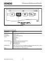
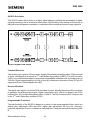
1
ICs for Communications
Signal Processing Codec Filter
SICOFI®, SICOFI®-2
User’s Manual 03.92
PEB 2060; PEB 2260
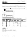
Revision History:
Original Version 03.92
Previous Releases:
Page
Subjects (changes since last revision)
Edition 03.92
This edition was realized using the software system FrameMaker.
Published by Siemens AG, Bereich Halbleiter, Marketing-Kommunikation,
Balanstraße 73, D-8000 München 80
© Siemens AG 1992. All Rights Reserved.
As far as patents or other rights of third parties are concerned, liability is only assumed for components per se,
not for applications, processes and circuits implemented within components or assemblies.
The information describes the type of component and shall not be considered as assured characteristics.
Terms of delivery and rights to change design reserved.
For questions on technology, delivery, and prices please contact the Offices of Semiconductor Group in Germany
or the Siemens Companies and Representatives worldwide (see address list).
Due to technical requirements components may contain dangerous substances. For information on the type in
question please contact your nearest Siemens Office, Semiconductor Group.
Siemens AG is an approved CECC manufacturer.
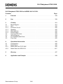
Contents
Table of Contents
Page
Introduction ...................................................................................................................... 5
General Information ......................................................................................................... 6
1
Type-Designation Code for ICs........................................................................... 6
2
Mounting Instructions .......................................................................................... 6
3
Processing Guidelines for ICs............................................................................. 7
4
Data Classification .............................................................................................. 12
5
Quality Assurance ............................................................................................... 12
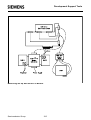
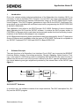
Overview on Architecture and Devices.......................................................................... 16
1
General Exchange Architecture .......................................................................... 16
1.1
Analog Line Cards............................................................................................... 17
1.2
Optimized Line Board Architecture ..................................................................... 19
1.3
The SLD / IOM®-2 Interface ................................................................................ 20
2
Device Overview ................................................................................................. 23
2.1
PCM Interface Controller (PBC / PIC / EPIC®) ................................................... 23
2.2
Signal Processing Codec/Filter (SICOFI® / SICOFI®-2) ..................................... 24
3
Advantages of Siemens Semiconductor Analog Line Card Concept .................. 29
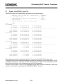
Functional Description and Technical Data of SICOFI® and SICOFI®-2 ..................... 30
SICOFI® PEB 2060 ............................................................................................................ 30
SICOFI®-2 PEB 2260......................................................................................................... 63
Package Outlines ............................................................................................................... 112
Development Support Tools ........................................................................................... 113
1
General Overview on Hardware / Software Tools............................................... 113
2
SICOFI® Coefficients Program (STS 2060) ........................................................ 115
2.1
Features .............................................................................................................. 115
2.2
General Overview ............................................................................................... 115
3
SICOFI® Test Board (STUT 2060)..................................................................... 117
3.1
Features .............................................................................................................. 117
3.2
General Overview ............................................................................................... 117
4
SICOFI®-2 Module (SIPB 5135).......................................................................... 119
4.1
Features .............................................................................................................. 119
4.2
General Overview ............................................................................................... 119
Detailed Description of Software Tools ......................................................................... 121
Software Description STS 2060 ......................................................................................... 121
Calculating SLIC Parameters of the Transformer SLIC
using M-Parameters and SPICE ........................................................................................ 225
Calculating SLIC Transfer Functions of the ERICSSON SLIC PBL 3736
Using K-Parameters and SPICE ........................................................................................ 268
Semiconductor Group
3
Contents
Table of Contents (cont’d)
Page
Detailed Description of Hardware Tools........................................................................ 326
SICOFI® Test Board STUT 2060...................................................................................... 326
SICOFI®-2 Module for the Siemens ISDN PC User Board (SIPB 5135) ........................... 358
SLIC Babyboard STUS 5502 for HARRIS SLIC HC 5502................................................. 386
SLIC Babyboard STUS 5509 for HARRIS SLIC HC 5509................................................. 398
SLIC Babyboard STUS 3762 for ERICSSON SLIC PBL 3736 .......................................... 411
SLIC Babyboard STUS 3762 for ERICSSON SLIC PBL 3762/64 ..................................... 423
SLIC Babyboard STUS 3030 for STM SLIC L3000 / L3030 .............................................. 437
SLIC Babyboard STUS 3090 for STM SLIC L3000 / L3090 .............................................. 453
SLIC Babyboard STUS 1001 for Transformer SLIC .......................................................... 466
Application Notes ............................................................................................................ 475
I
SICOFI® Application Together with HARRIS-SLIC HC 5502 ............................ 475
II
SICOFI® Application Together with ERICSSON SLIC PBL 3762...................... 502
III
SICOFI® Application Together with STM SLIC L3000 /L3030........................... 548
IV
SICOFI® Application Together with STM SLIC L3000 /L3090........................... 594
V
SICOFI® Application Together with Transformer SLIC with
Series Feeding.................................................................................................... 629
VI
SICOFI® Application Together with Transformer SLIC
with Transverse Feeding .................................................................................... 658
VII
SICOFI® Application Together with Transformer SLIC
for USA Specification.......................................................................................... 710
VIII
SICOFI® Layout Recommendation for Analog Line-Card Applications ............. 723
IX
Using SICOFI®-2 (PEB 2260) in IOM®-2 Mode .................................................. 728
X
DAML Simulation Using the SIPB 5000 Userboard System............................... 744
IOM®, IOM®-1, IOM®-2, SICOFI®, SICOFI®-2, SICOFI®-4, SICOFI®-4µC, SLICOFI®, ARCOFI® , ARCOFI®-BA, ARCOFI®-SP,
EPIC®-1, EPIC®-S, ELIC®, IPAT®-2, ITAC®, ISAC®-S, ISAC®-S TE, ISAC®-P, ISAC®-P TE, IDEC®, SICAT®, OCTAT®-P,
QUAT®-S are registered trademarks of Siemens AG.
MUSAC™-A, FALC™54, IWE™, SARE™, UTPT™, ASM™, ASP™ are trademarks of Siemens AG.
Purchase of Siemens I2C components conveys a license under the Philips’ I2C patent to use the components in the I2C-system
provided the system conforms to the I2C specifications defined by Philips. Copyright Philips 1983.
Semiconductor Group
4
Contents
Introduction
The following chapters inform you about the technical data and programming of the Signal
Processing Codec Filter SICOFI® / SICOFI®-2 PEB 2060/2260 and describe the hardware and
software tools. Application notes show you how to use and work with the SICOFI family in a
given application.
In order to get an overview of the architecture, the devices and the tools, we suggest to start
having a look at the ’General Overview on Architectures and Devices’ as well as ’Development
Support Tools’.
Detailed descriptions can be found in the other chapters.
For more information on related products and quality issues we provide the information on
literature.
Semiconductor Group
5
General Information
✥✥
1
Type-Designation Code for ICs
IC type designations are based on the European Pro Electron system. The code system is
explained in the Pro Electron brochure D 15*), edition 1988.
*) Available from Pro Electron
Avenue Louise, 430 (B.12)
B -1050 Bruxelles, Belgium
2
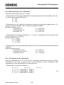
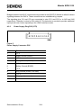
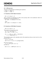
Mounting Instructions
Plastic Packages for Insertion
The pins of the packages are bent downwards by an angle of 90° and fit into holes on a
grid of 2.54 mm and with diameters of between 0.7 and 0.9 mm. The dimension x is shown
in the corresponding drawing of the package.
The bottom of the package will not touch the circuit board after insertion because the pins
have shoulders just below the package (see figure 1).
After insertion of a package on a board it is advisable to bend the ends of two pins at an
angle of approx. 30° to the board so that the package does not have to be pressed down
during soldering.
Plastic packages are soldered on the board on the side facing away from the package.
The maximum permissible soldering temperature is 260 °C (max.10 s) when using a solder
bath, e.g. wave soldering, and 350 °C (max. 3 s) when using a soldering iron.
ws
Figure 1
Plastic Packages (P-DSO and P-LCC) for Surface Mounting (SMD)
Reflow soldering:
for a device temperature of 215 °C max. soldering time 2 x 40 s
(typical figure for vapor-phase soldering)
Wave soldering:
soldering temperature 260 °C,
soldering time max. 10 s.
Soldering iron:
the minimum thermal stress, based on experience, is at a
soldering temperature of 350 °C (soldering time ≤ 3 s)
Semiconductor Group
6
General Information
Storage and Pretreatment of SMD ICs
The components should be stored in a dry place. Some large and specially identified plastic
ICs have to be processed in a dry condition. This is produced by dry packing or by means
of a separate drying process shortly before they are processed (e.g. 16 h at 125 °C)
3
Processing Guidelines for ICs
Integrated circuits (ICs) are electrostatic-sensitive (ESS) devices. The demand for
greater packing density has led to smaller structures on semiconductor chips, with the
result that today every IC, whether bipolar, MOS, or CMOS, has to be protected against
electrostatics.
MOS and CMOS devices generally have integrated protective circuits and it is virtually
impossible for them to be destroyed by purely static electricity. On the other hand, there
is acute danger from electrostatic discharges (ESD).
Of the multitude of possible sources of discharge, charged devices should be mentioned
in addition to charged persons. Low-resistive discharges can produce peak powers
amounting to kilowatts.
For the protection of devices the following principles should be observed:
a)
Reduction of charging voltage, below 200 V if possible.
Means which are effective here are an increase in relative humidity to ≥ 60 % and
the replacement of highly charging plastics by antistatic materials.
b)
With every kind of contact with the device pins a charge equalization is to be
expected. This should always be highly resistive (ideally R = 106 to 109 Ω).
All in all this means that ICs call for special handling, because uncontrolled charges,
voltages from ungrounded equipment or persons, surge voltage spikes and similar
influences can destroy a device. Even if devices have protective circuits (e.g. protective
diodes) on their inputs, the following guidelines for their handling should nevertheless be
observed.
Identification
The packing of ESS devices is provided with the following label by the
manufacturer:
Scope
The guidelines apply to the storage, transport, testing, and processing of all kinds of ICs,
equipped and soldered circuit boards that comprise such components.
Semiconductor Group
7
General Information
Handling of Devices
1
ICs must be left in their containers until they are processed.
2
ICs may only be handled at specially equipped work stations. These stations must
have work surfaces covered with a conductive material of the order of 106 to109 Ω/cm.
3
With humidity of > 50 % a coat of pure cotton is sufficient. In the case of
chargeablesynthetic fibers the clothing should be worn close-fitting. The wrist strap
must be worn snugly on the skin and be grounded across a resistor of 50 kΩ to 100 kΩ.
4
If conductive floors, R = 5 × 10⁴ to 107 Ω are provided, further protection can be achieved
by using so-called MOS chairs and shoes with a conductive sole (R ≈ 105 to 107 Ω).
5
All transport containers for ESS devices and assembled circuit boards must first be
brought to the same potential by being placed on the work surface or touched by the
operator before the individual devices may be handled. The potential equalization
should be across a resistor of 105 to 108 Ω.
6
When loading machines and production devices it is necessary to ensure that the
devices do not come out of the transport magazine charged and that they are not
damaged by touching metal, e.g. parts of a machine.
Example 1
conductive (black) tubes.
The devices may be destroyed in the tube by charged persons or come
out of the tube charged if this is emptied by a charged person.
Conductive tubes may only be handled at ESS work stations
(high-resistance work-station and person grounding).
Example 2) anti-static (transparent) tubes.
The devices cannot be destroyed in the tube by charged persons (there
may be a rare exception in the case of custom ICs with unprotected gate
pins). The devices can be endangered as in 1) when the tube is emptied
if the latter, especially at low humidity, is no longer sufficiently
anti-static after a long period of storage (> 1 year).
In both cases damage can be avoided by discharging the devices across a grounded
adapter of high-resistance material (≈ 106 to 108 Ω/cm) between the tube and the machine.
The use of metal tubes – especially of anodized aluminium – is not advisable because of
the danger of low-resistance device discharge.
Semiconductor Group
8
General Information
Storage
ESS devices should only be stored in identified locations provided for the purpose.
During storage the devices should remain in the packing in which they are supplied.
The storage temperature should not exceed 30 °C.
Transport
ESS devices in approved packing tubes should only be transported in suitable containers
of conductive or longterm anti-static-treated plastic or possibly unvarnished wood.
Containers of both high-charging plastic or very low-resistance materials are unsuitable.
Transfer cars and their rollers should exhibit adequate electrical conductivity
(R < 106 Ω). Sliding contacts and grounding chains will not reliably eliminate charges.
Incoming Inspection
In incoming inspection the above guidelines should be observed. Otherwise any right to
refund or replacement if devices fail inspection may be lost.
Material and Mounting
1
The drive belts of machines used for the processing of the devices, in as much as they
come into contact with them (e.g. bending and cutting machines, conveyor
belts), should be treated with anti-static spray (e.g. anti-static spray 100 from
Kontaktchemie). It is better, however, to avoid the contact completely.
2
If ESS devices have to be soldered or desoldered manually, soldering irons with
thyristor control may not be used. Siemens EMI-suppression capacitors of the type
B 81711-B31…–B36 have been proven very effective against line transients.
3
Circuit boards fitted and soldered with ESS devices are always to be considered as
endangered.
Semiconductor Group
9
General Information
Electrical Tests and Application Circuit
1
The devices should be processed with observation of these guidelines. Before
assembled and soldered circuit boards are tested, remove any shorting rings.
2
The sockets or integrated circuits must not be conducting any voltage when individual
devices or assembled circuit boards are inserted or withdrawn, unless works
specifications state otherwise. Ensure that the test devices and power supplies do not
produce any voltage spikes, either when being turned on and off in normal operation
or if the power fuse blows or other fuses respond.
3
When supplying bipolar integrated circuits with current, the negative voltage
(–V S or GND) has first to be connected. In general, an interruption of this potential
during operation is not permissible.
4
Signal voltages may only be applied to the inputs of ICs when or better after the supply
voltage is turned on. They must be disconnected when or better before the supply
voltage is turned off.
5
Power supplies of integrated circuits are to be blocked as near as possible at the
supply terminals of the IC. With bipolar ICs it is recommended to use a low-inductance
electrolytic capacitor or at least a paralleled ceramic capacitor of 100 nF to 470 nF for
example.
Using ICs with high output currents, the necessary value of the electrolytic capacitor
must be adapted to the test or application circuit. Transient behavior and dynamic
output resistance of the power supplies, line inductances in the supply and load circuit
and in particular inductive loads or motors have to be considered.
When switching off line inductances of inducitve loads, the stored power has to be
consumed externally, unless otherwise specified (e.g. by an electrolytic capacitor,
diodes, Z-diodes or the power supply). Also a switching off of the supply voltage prior
to the load rejection should be taken into account.
6
ICs with low-pass character of the output stages (e.g. PNP drivers or PNP/NPN endstages), normally need an additional external compensation at the output. This applies
particularly to complex loads. The output of AF power amplifiers is compensated by the
Boucherot element. In individual cases, bridge circuits only need a capacitance for
bypassing the load. Depending on the application it is, however, also recommended to
connect one capacitor from each output to ground.
7
Observe any notes and instructions in the respective data books.
Semiconductor Group
10
General Information
Packing of Assembled PC Boards or Flatpack Units
The packing material should exhibit low volume conductivity:
105 Ω/cm < p < 1010 Ω/cm.
In most cases – especially with humidity of > 40 % – this requirement is fulfilled by a simple
corrugated board.
Better protection is obtained with bags of conducitve polyethylene foam (e.g. RCAS 1200
from Richmond of Redlands, California).
You should always ensure that different boards cannot touch.
In special cases it may be necessary to provide protection against strong electric fields,
such as can be generated by conveyor belts for example.
For this purpose a sheath of aluminium foil is recommended, although direct contact
between the film and the PCB must be avoided.
Cardboard boxes with an aluminium-foil lining, such as those used for shipping our devices,
are available from Laber of Munich.
Ultrasonic Cleaning of ICs
The following recommendation applies to plastic packages. For cavity packages (metal and
also ceramic) separate regulations have to be observed.
Freon and isopropyl alcohol (trade name: propanol) can be used as solvents. These
solvents can also be used for plastic packages because they do not eat into the plastic
material.
An ultrasonic bath in double halfwave operation is advisable because of the low component
stress.
The ultrasonic limits are as follows:
sound frequency
exposure
alternating sound pressure
sound power
Semiconductor Group
f > 40 kHz
t < 2 min
p < 29 kPa
N < 0.5 W/cm2/liter
11
General Information
4
Data Classification
Maximum Ratings
Maximum ratings are absolute ratings; exceeding any one of these values may cause
irreversible damage to the integrated circuit.
Characteristics
The listed characteristics are ensured over the operating range of the integrated circuit.
Typical characteristics specify mean values expected over the production spread. If not
otherwise specified, typical characteristics apply at TA = 25 °C and the given supply voltage.
Operating Range
In the operating range the functions given in the circuit description are fulfilled.
5
Quality Assurance
Quality Assurance System
The high quality and reliability of integrated circuits from Siemens are the results of
carefully managed design and production which is systematically checked and controlled at
each stage.
The procedures are subject to a quality assurance system; full details are given in the
brochure "Quality Assurance – Integrated Circuits".
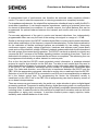
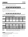
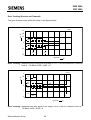
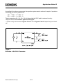
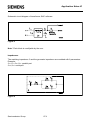
Figure 1 and 2 show the most important stages of Quality Assurance (QA) system. QA
departments independent of production and development are responsible for the selected
measures, acceptance procedures and information feedback loops. Operating QA
departments have state-of-the-art test and measuring equipment at their disposal, work
according to approved methods of statistical quality control, and are provided with facilities
for accelerate life and environmental tests used for both qualification and routine monitoring
tests.
The latest methods and equipment for preparation and analysis are employed to achieve
continuity of quality and reliability.
Conformance
Each integrated circuit is subjected to a final test at the end of the production process.
These are carried out by computer-controlled, automatic test systems because hundreds of
thousands of operating conditions as well as a large number of static and dynamic
parameters have to be considered. Moreover, the test systems are extremely reliable and
reproducible. The QA department carries out a final check in the form of a lot-by-lot
sampling inspection to additionally ensure this minimum percent defectives to ensure
statistically that the PDA of released lots is less than the AQL agreed. Sampling inspection
is performed in accordance with the inspection plans of DIN 40 080, as well as of the
identical MIL-STD-105 or IEC 410.
Semiconductor Group
12
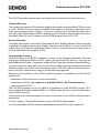
General Information
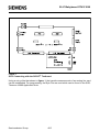
Figure 2
Semiconductor Group
13
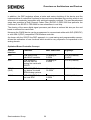
General Information
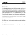
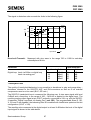
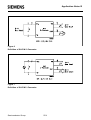
Figure 3
Reliability
Measures Taken During Development
The reliability of ICs is already considerably influenced at the development stage. Siemens
has, therefore, fixed certain design standards for the development of circuit and layout, e.g.
specifying minimum width and spacing of conductive layers on a chip, dimensions and
electrical parameters of protective circuits for electrostatic charge, etc. An examination with
the aid of carefully arranged programs operated on large-scale computers, guarantees the
immediate identification and elimination of unintentional violations of these designs
standards.
Semiconductor Group
14
General Information
In-Process Control During Production
The manufacturing of integrated circuits comprises several hundred production steps. As
each step is to be executed with utmost accuracy, the in-procress control is of outstanding
importance. Some processes require more than a hundred different test measures. The
tests have been arranged in a manner that the individual steps of the process can be
reproduced continuously.
The decreasing failure rates reflect the persistent effort in this direction; in the course of the
years they have been reduced considerably despite an immense rise in IC complexity.
Reliability Monitoring
The general course of the IC failure rate versus time is shown by a so-called "bathtub"
curve. The failure rate has its peak during the first few operating hours (early failure period).
After the early failure period has decayed, the "constant" failure rate period starts during
which the failures may occur at an approximately uniform rate. This period ends with a
repeated rise of the curve during the wear-out failure period. For ICs, however, the latter
period usually lies far beyond the service life specified for the individual equipment.
Reliability tests for ICs are usually destructive examinations. They are, therefore, carried
out with samples. Most failure mechanisms can be accelerated by means of higher
temperatures. Due to the temperature dependence of the failure mechanisms, it is possible
to simulate future operational behavior within a short time by applying high temperatures;
this is called life test.
The acceleration factor B for the life test can be obtained from the Arrhenius equation
( (
B = exp EA 1 - 1
k T1
T2
))
where T2 is the temperature at which the life test is performed, T1 is the assumed operating
temperature, and k is the Boltzmann constant.
Important for factor B is the activation energy EA. It lies between 0.3 and 1.3 eV and differs
considerably for the individual failure mechanisms.
For all Siemens ICs, the reliability data gained from life tests are converted to an operating
temperature of TA = 55 °C, assuming an average activation energy of 0.5 eV. The
acceleration factor for life tests at 125 °C is thus 24, compared with operational behavior.
This method also considers failure mechanisms with low activation energy, i.e. which are
only slightly accelerated by the temperature effect.
Various reliability tests are periodically performed with IC types that are representative of a
certain production line – this is described in the brochure "Quality Assurance-Integrated
Circuits". Such tests are e.g. humidity test at 85 °C and 85 % relative humidity, pressure
cooker test, as well as life tests up to 1000 hours and more. Test results are available in the
form of summary reports.
Semiconductor Group
15
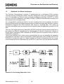
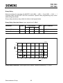
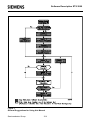
Overview on Architecture and Devices
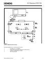
1
General Exchange Architecture
Semiconductor Group
16
Overview on Architecture and Devices
1.1
Analog Line Cards
In a digital exchange system the subscriber line boards provide the link between the subscriber
and the switching network. The basic functions of analog line boards are known under the
acronym BORSHT (battery, overvoltage, ringing, supervision, hybrid, testing). Moreover,
further important tasks are voice frequency band limitation, analog to digital conversion into
time discrete digital equivalents, time-slot assignment on the PCM highways and handling of
signaling and control information.
Usual implementation uses two PCM ports and one µP interface per subscriber line leading
to a large amount of wiring and, thus, problems such as crosstalk and large board size.
Usual implementation is also characterized by fixed adjustment of line interface conditions
although telephone line conditions vary considerably with national standards and even with
subscriber line installations. Under adverse conditions telecommunication equipment must
match the subscriber line and termination impedances while suppressing return echoes in the
two- to four-wire hybrid network. Compensating for line attenuation is just as critical for
balancing the voice signals in the transmission and reception paths.
To improve voice quality, subscriber line boards have to be matched to different line conditions
by means of interchangeable discrete components. This approach is very costly regarding line
board design and manufacturing. Furthermore, the reliability of a board filled with parts, wires
and connections will decrease rapidly.
The subscriber line board architecture proposed by Siemens Semiconductor is geared to
eliminate many of these line board trouble spots.
Semiconductor Group
17
Overview on Architecture and Devices
General Line Board Structure and Functions
General Line Card Function
Component
Function
SLIC
(Subscriber
line interface
circuit)
realisation of the BORSHT function
B battery feed
O overvoltage protection
R ringing
S supervision
H hybrid
T testing
analog network Z
matching of input and line impedance
R,X frequency response correction
B
hybrid balancing
G
gain adjustment
CODEC/Filter
coding, A/D and D/A conversion according to A-law and µ-law, voice
band limitation according to CCITT and LSSGR
PCM
time-slot assignment, PCM data rate
Semiconductor Group
18
Overview on Architecture and Devices
1.2
Optimized Line Board Architecture
The Siemens Semiconductor concept is characterized by a centralized PCM interface
controller device providing the variable Time-Slot Assignment (TSA), the communication with
up to 64 subscriber line devices such as signal processing codec/filter (SICOFI®) or ISDN
devices via the SLD (Subscriber Line Data) or IOM®-2 (ISDN Oriented Modular) interface, and
the interface with a microprocessor.
As a characteristic architectural feature, for test, monitring and control purposes, the device
permits efficient switching of data streams between all these interfaces and, therefore, ensures
transparency between the PCM channels and control or signaling data. This opens up
attractive possibilities such as common-channel signaling and microprocessor access to PCM
data.
The use of the signal processing codec/filter (SICOFI) avoids the analog network which has to
be matched to different requirements by interchanging its discrete components. Based on
Digital Signal Processing (DSP) methods the SICOFI allows the complete control of the line
conditions by software.
The all-over flexibility of the unique device concept gives the user the capability for designing
a standard line card which can be customized for each application under software control. The
SLD/IOM-2 architecture leads to a highly modular line board configuration with low wiring,
reduced board area and, depending only on the SLIC to be used, very few discrete elements.
Siemens ICs for Analog Subscriber Lines
Semiconductor Group
19
Overview on Architecture and Devices
1.3
The SLD/IOM®-2 Interface
The SLD bus is used by the PBC/PIC to interface with the subscriber line devices. A Serial
Interface Port (SIP) is used for the transfer of all digital voice and data, feature control and
signaling information between the individual subscriber line devices, the PCM highways and
the control backplane. The SLD approach provides a common interface for analog or digital
per-line components. Through the PBC/PIC, which is the key device in the SLD architecture,
the PCM data is transparently switched onto the PCM highways. The PBC will make analog
and digital subscriber line boards plug-compatible in a line equipment rack.
There are three leads connecting each subscriber line device and the PBC/PIC: two common
clock signals shared among all devices, and a unique bidirectional data lead for each of the
eight SIP lines. The Direction signal (DIR) is an 8-kHz clock output from the PBC (master) that
serves as a frame sync to the subscriber line devices (slave) as well as a transfer indicator.
The data are transferred at a 512-kHz rate, clocked by the Subscriber Clock (SCLK). When
DIR is high (first half of the SLD 125 µs frame), four bytes of digital data are transmitted on the
SLD bus from the PBC/PIC to the slave (receive direction). During the second half of the frame
when DIR is low, four bytes of data are transferred from the slave back to the PBC/PIC
(transmit direction).
Channel A and B are 64-kbit/s channels reserved for voice or data to be routed to and from the
PCM highways. In an application where one SICOFI is connected to a SIP, voice is received
on channel A and transmitted on channel A and B. For a three-party conference, channel B is
the third-party voice channel. If two SICOFIs are connected to one SIP, channel A is assigned
to one and channel B to the other SICOFI. Conferencing is not possible in this configuration.
With digital subscriber line devices the two bytes can be used to carry 64-kbit/s data channels.
The third and sixth byte locations are used to transmit and receive control information for
programming the slave devices. The last byte in each direction is reserved for signaling data.
Semiconductor Group
20
Overview on Architecture and Devices
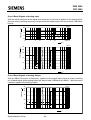
Frame Structure of the SLD Interface
Because of the unique requirements of ISDN systems, Siemens developed an interchip
interface especially for these applications. As part of their joint definition of ISDN components,
the "Group of Four" (ALCATEL, Siemens, Plessey and ITALTEL systems houses) adapted this
Siemens Semiconductor interface and suggested some compatible additional features. The
resulting IOM-2 interface has become the standard for interchip communication in ISDN
terminals, terminal adaptors, network terminations, transmission repeaters and line cards for
digital exchange systems.
The IOM-2 interface is a four wire interface with: a bit clock, a frame clock and one data line
per direction. It has a flexible data clock. In this way, data transmission requirements are
optimized for different applications.
Semiconductor Group
21
Overview on Architecture and Devices
On line cards, a 4096-kHz clock has been selected so that up to eight IOM channels and thus,
eight ISDN or 16 analog subscribers can be multiplexed over a single IOM-2 bus. The channel
structure of the IOM-2 interface is as follows:
The first two octets constitute the two 64 kbit/s B channels.
● The third octet is the MONITOR channel. It is used for the exchange of data between
devices using the IOM-2 MONITOR channel protocol.
●
●
The fourth octet (control channel) contains
– two bits for the 16 kbit/s D channel
– a four-bit command/indication channel, in ISDN applications or
– a six bit command/indication channel for analog subscriber applications
– two bits MR and MX for supporting the MONITOR channel protocol.
Multiplexed Frame Structure of the IOM®-2 Interface
Semiconductor Group
22
Overview on Architecture and Devices
2
Device Overview
2.1
PCM Interface Controller (PBC/PIC/EPIC®)
The key device in the SLD architecture is the Peripheral Board Controller (PBC) PEB 2050.
Basically the PBC is a highly intelligent multiplexer/demultiplexer chip which performs the
variable time-slot assignment for up to 16 PCM channels and handles the data streams for
control and signaling. It constitutes the interface between the subscriber line devices such as
codec filter or ISDN communication controller, the PCM lines, the central control unit and the
optional onboard microprocessor.
Due to the importance of reliability in system design, the PBC provides a backplane interface
with two fully redundant PCM highways. For the exchange of information between a central
control unit and the PBC working as a "slave" in a point-to-multipoint configuration, the device
supports a subset of the CCITT’s High Level Data Link Control (HDLC) communications
protocol so that it can respond to certain HDLC frames without microprocessor intervention or
software supervision.
The hardwired implementation of the physical level of the HDLC protocol (e.g. cyclic
redundancy check) and of parts of this logical level (e.g. evaluation of HDLC commands and
preparation of response packets) in the on-chip HDLC controller permits very high data rates
of up to 4 Mbaud via the serial link to the central processor. By using a local standard
microprocessor, such as the SAB 8051, it is possible to expand the range of the HDLC protocol
to the full X.25 level, while still maintaining procedure handling, buffering and distribution of
data packets hardwired in the PBC. Furthermore, the PBC is able, in conjunction with a
microprocessor, to take over the "primary" function of a high speed HDLC communication link.
The PBC communicates with the subscriber line devices via a three-wire subscriber line data
(SLD) bus based on a ping-pong type of protocol. The SLD bus ensures reduced line board
wiring.
To cover a broad range of applications the PBC is adaptable to all standard commercial PCM
systems (with 24, 32, 48, 64 channels per frame). Independently of the system clock used, the
circuit computes all timing signals required for the standardized SLD bus, thus decoupling the
subscriber line devices from the system clock. The PBC is an excellent example of the efficient
realization of standard functions through the use of hardwired logic in order to increase
realtime processing and speed without loss of flexibility.
A further device for interfacing subscriber line devices with PCM lines is the PCM Interface
Controller (PIC) PEB 2052. This CMOS device performs the Time-Slot Assignment (TSA)
and the PCM interface functions. It is pin and software-compatible to the PBC PEB 2050, but
leaves out the HDLC controller and the hardwired Last Look Logic.
Semiconductor Group
23
Overview on Architecture and Devices
The Extended PCM Interface Controller (EPIC) PEB 2055 is intended to be used as central
PCM processor in the IOM architecture. The CMOS device can be programmed to operate at
different data rates between 128 and 8192 kbit/s. The system interface consists of up to four
duplex ports with a tristate indication signal for each output line. The configurable interface can
be selected to incorporate either four duplex (IOM) or eight bidirectional I/O ports (SLD).
The EPIC can therefore be programmed to communicate either with SLD or with IOM (ISDN
Oriented Modular) and IOM®-2 compatible devices. In both cases the device handles the layer1 functions of buffering the C/I and MONITOR channels for IOM-compatible devices and the
feature control and signaling channels for SLD compatible devices. The EPIC can handle up
to 32 ISDN subscribers with their 2B + D channel structure or 64 analog subscribers in IOM
configuration or up to 16 subscribers in SLD configuration. Since its interfaces can operate at
different data rates, the EPIC is an ideal device for data rate adaptation.
Moreover, the EPIC is one of the fundamental building blocks for networks with either central,
decentral or mixed signaling and packet data handling architectures.
The EPIC-2 PEB 2056 is a smaller version of the EPIC. The functions that are performed
remain essentially the same but the EPIC-2 PEB 2056 has been optimized for time-slot
assignment and switching functions on line cards with up to 8 ISDN or 16 analog subscriber
lines.
Siemens Semiconductor therefore offers the optimal solution of PCM Interface Controller for
every application.
– PBC PEB 2050:
for up to eight ISDN and 16 analog subscribers. Especially suitable for
powerful PABX.
– PIC PEB 2052:
for up to eight ISDN and 16 analog subscribers. Ideal for price
sensitive systems, e.g. small PABX and public exchanges (CO).
– EPIC PEB 2055:
for up to 32 ISDN and 64 analog subscribers. Suitable as the central
PCM processor in IOM architectures.
– EPIC-2 PEB 2056: for up to 8 ISDN or 16 analog subscribers in IOM architectures.
2.2
Signal Processing Codec/Filter (SICOFI®/SICOFI®-2)
The Codec/Filter used in the advantageous analog line board architecture is the
programmable Signal Processing Codec Filter (SICOFI) PEB 2060, fabricated in advanced
CMOS technology. Based on Digital Signal Processing (DSP) methods, in addition to the
standard functions of PCM coding and voice-band limitation that any codec filter features, the
SICOFI provides a variety of user-programmable filters for impedance matching, 2/4-wire
hybrid balancing, analog and digital gain adjustment as well as frequency response correction.
Semiconductor Group
24
Overview on Architecture and Devices
A sophisticated level of performance can therefore be achieved under complete software
control. The use of external components or trimming procedures is completely avoided.
For impedance adjustments, the related filter implements a feedback loop to modify the SLIC’s
termination impedance. It can handle complex impedances, resulting in optimized return loss
for almost all subscriber line conditions. In a similar manner, the hybrid balance filter can be
programmed for optimal balance between the transmit and receive side and for minimum
echoes.
For accurate adjustment of the gain in receive and transmit directions, four independently
programmable filters can vary the level of the analog voice signal in a range of ± 22 dB.
Similar to the level control, the SICOFI contains digital filters in receive and transmit directions,
which allow modification of the frequency response characteristics. Further features attractive
for the realization of flexible exchange systems are selectable A/µ law coding, three-party
conference support, supply voltage supervision, hardware and software reset, power-down
mode and on-chip reference voltage. Different loopback modes enable both the line board and
the total system to be tested during operation. The SICOFI can hook up directly to virtually any
commercial SLIC, because of its flexible signaling interface consisting of ten ports. Three are
dedicated to the status of voice transmissions and three to receptions. The remaining four can
be programmed individually as either transmit or receive ports.
Due to the fact that the SICOFI needs extended control information, a message-oriented
protocol is used for byte transfer via the SLD bus. Two bits in each control byte are used to
define three different classes of commands, which contain information about the configuration
of the SICOFI, the coefficient exchange and the number of subsequently transmitted data
bytes. Per frame and direction, one control byte is transferred between the SICOFI and the
PBC. With the appropriate commands, data can be written into or read back from the SICOFI.
Selection of one of the two SICOFIs connected to one SLD port is accomplished by an address
bit in the feature control byte. For programming the device the information usually is
transferred via the HDLC link to the PBC, but all programming can also be done by means of
an on-board microprocessor.
There are numerous good reasons why, the world over, major attention is given to digital signal
processing methods. Compared to analog filtering, digital processing does not need precision
elements, allows much higher accuracy along with precisely predictable transmission behavior
including noise. It makes the device less sensitive to parameter fluctuations such as drift with
temperature or aging and, moreover, it provides excellent power supply rejection, better
testability and crosstalk behavior of the circuit.
Semiconductor Group
25
Overview on Architecture and Devices
In addition, the DSP technique allows a better and easier shrinking of the device and the
implementation of codec/filter functions for two and more subscribers on one chip, which is not
economic or completely impossible with switched capacitor methods. The next development
stage has produced a Dual Channel Codec Filter (SICOFI-2) PEB 2260 that performs the
functions of the SICOFI-1 PEB 2060 for two subscribers in one chip.
The sharing of the same digital signal processor part allows a reduced die size per line and
leads to reduced line-card costs.
Moreover the CMOS device can be programmed to communicate either with SLD (PBC/PIC)
or with IOM-2 (EPIC) compatible PCM interface controller.
As shown with the SICOFI the DSP approach, in a cost-saving and programmable manner,
allows the realization of new functions which would be very expensive or impractical in the
analog domain.
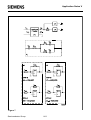
Optimized Board Controller Concept
Circuit
Interface
Controller
Max. Subscriber
Highways
SLD
PEB 2050 (PCB)
with HDLC controller
16 analog or
8 ISDN
2 PCM (4 Mbit/s)
1 HDLC
SLD
PEB 2052 (PIC)
low cost PBC for
analog line cards with
SICOFI
16 analog or
8 ISDN
2 PCM (4 Mbit/s)
IOM-2/
(SLD)
PEB 2055 (EPIC-1)
key device for mixed
ISDN/Analog systems
64 analog or
32 ISDN
4 PCM (8 Mbit/s)
IOM-2
PEB 2056 (EPIC-2)
low cost EPIC
16 analog or
8 ISDN
2 PCM (4 Mbit/s)
Semiconductor Group
26
Overview on Architecture and Devices
Optimal Solutions for Every Application
Semiconductor Group
27
Overview on Architecture and Devices
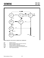
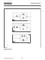
Mixed Use of ISDN and Analog Subscribers with EPIC®
Semiconductor Group
28
Overview on Architecture and Devices
3
Advantages of Siemens Semiconductor Analog Line Card Concept
●
Advanced Signal Processing Codec Filter SICOFI family based on DSP technique.
●
Matching to different line conditions under complete software control (global line-card
solution).
●
Modular architecture (IOM-2/SLD compatible).
●
Reduced line card wiring, per line structure avoids cross wiring.
●
Optimized board controller family.
●
Cost optimized design/high volume production.
●
Effective application support tools (hardware/software).
Semiconductor Group
29
Signal Processing Codec Filter (SICOFI®)
PEB 2060
Features
●
●
●
●
●
●
●
●
●
●
●
●
●
●
●
●
●
●
CMOS IC
Single chip codec and filter
Band limitation according to all CCITT
and AT & T recommendations
Digital Signal Processing techniques
Digital voice transmission
– PCM encoded (A-law or µ-law)
– linear (16 bit 2's complement)
Programmable digital filters for
– impedance matching
– transhybrid balancing
– gain
– frequency response correction
Configurable three pin serial interface
– 512-kHz-SLD-Bus (e.g. to PEB 2050/52)
– burst mode with bit rates up to 4 Mbit/s
Programmable signaling interface
to peripherals (e.g. SLIC)
High performance A/D and D/A conversion
Programmable analog gain
Advanced test capabilities
– three digital loop back modes
– two analog loop back modes
– on chip tone generation
No trimming or adjustments
No external components
Variable clock selection
Signaling expansion possible
Prepared for three-party conferencing
Advanced low power 2µCMOS technology
Power supply + / – 5 V
Meets or exceeds CCITT
and LSSGR recommendations
P-LCC-28-R
P-DIP-22
Type
Version
Ordering Code
Package
PEB 2060-N
V 4.4
Q67100-H8393
P-LCC-28-R (SMD)
PEB 2060-P
V 4.4
Q67100-Z170
P-DIP-22
Semiconductor Group
30
03.92
PEB 2060
General Description
The Signal Processing Codec Filter (SICOFI) PEB 2060 is a fully integrated PCM codec
(coder/decoder) and transmit/receive filter fabricated in advanced CMOS technology for
applications in digital telecommunication systems. Based on a digital filter concept, the PEB
2060 provides improved transmission performance and high flexibility. The digital signal
processing approach supports software controlled adjustment of the analog behavior,
including attractive features such as programmable transhybrid balancing, impedance
matching, gain and frequency response correction.
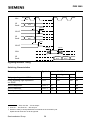
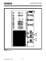
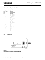
Pin Configuration
(top view)
P-LCC-28-R
Semiconductor Group
P-DIP-22
31
PEB 2060
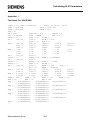
Pin Definitions and Functions
Pin No.
P-LCC-28-R P-DIP-22
Symbol
Input (I)
Function
Output (O)
1
1
V DD
I
+ 5 V power supply
6
4
V SS
I
– 5 V power supply
5
3
GNDA
I
Ground analog, not internally
connected to GNDD
All analog signals are referred to this pin
7
5
GNDD
I
Ground digital, not internally
connected to GNDA
All digital signals are referred to this pin
28
22
VIN
I
Analog voice input to transmit path
3
2
VOUT
O
Analog voice output of the received
digital voice
16
12
SCLK
I
Slave clock
13
10
DIR
I
Frame synchronisation signal
(direction signal)
21
17
SIP
I/O
Serial interface port, bidirectional
serial data port
12
9
RS
23
18
TEST
I
Test input, normally connected to GNDD
14
11
PLL
I
Clock selection (see Appendix A)
24
19
SI1
I
26
20
SI2
I
27
21
SI3
I
10
8
SO1
O
9
7
SO2
O
8
6
SO3
O
20
16
SA
I/O
19
15
SB
I/O
18
14
SC
I/O
17
13
SD
I/O
Semiconductor Group
Reset
I input, RS forces the SICOFI
to power down mode and initializes
the configuration registers
Signaling inputs. Data present at SI
is sampled and transmitted via
the serial interface
Signaling outputs. Data received via
the serial interface is latched
and fed to these outputs
Programmable I/O signaling pins.
Each of these pins may be declared
input individually with adequate
SICOFI status settings. If 2 SICOFIs
are connected to 1 serial interface,
pin SA (high/low) assigns voice,
control and signaling bytes
32
PEB 2060
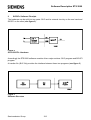
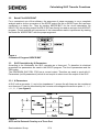
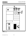
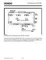
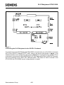
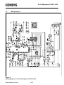
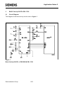
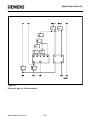
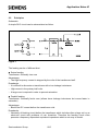
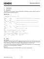
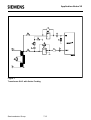
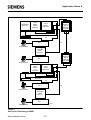
SICOFI® Principles
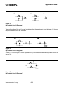
The SICOFI codec filter solution is a highly digital approach utilizing the advantages of digital
signal processing such as excellent performance, high flexibility, easy testing, no sensitivity to
fabrication and temperature variations, no problems with crosstalk and power supply rejection.
SICOFI® Signal Flow Graph
Transmit Direction
The analog input signal is A/D converted, digitally filtered and transmitted either PCM-encoded
or linear. Antialiasing is done with a 2nd order Sallen-Key prefilter (PREFI). The A/D Converter
(ADC) is a modified slopeadaptive interpolative sigmadelta modulator with a sampling rate of
128 kHz. Digital downsampling to 8 kHz is done by subsequent decimation filters D1 and D2
together with the PCM bandpass filter (BP).
Receive Direction
The digital input signal is received PCM-encoded or linear, digitally filtered and D/A converted
to generate the analog output signal. Digital interpolation up to 128 kHz is done by the PCM
lowpass filter (LP) and the interpolation filters I1 and I2. The D/A Converter (DAC) output is fed
to the 2nd order Sallen-Key postfilter (POFI).
Programmable Functions
The high flexibility of the SICOFI is based on a variety of user programmable filters, which are
analog gain adjustment AGR and AGX, digital gain adjustment GR and GX, frequency
response adjustment R and X, impedance matching filter Z and the transhybrid balancing filter
B.
Semiconductor Group
33
PEB 2060
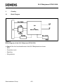
Signaling
SA...SD SI
SO
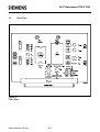
4
VIN
PREFI A
3
3
DIR
D
SCLK
Interface
SIP
S
L
D
B
U
S
DSP
Coeff.
RAM
VOUT
POFI D
A
ITB00635
SICOFI® Block Diagram
The SICOFI bridges the gap between analog and digital voice signal transmission in modern
telecommunication systems. High performance oversampling Analog-to-Digital Converter
(ADC) and Digital-to-Analog Converter (DAC) provide the conversion accuracy required. An
analog antialiasing prefilter (PREFI) and smoothing postfilter (POFI) is included. The
dedicated on chip Digital Signal Processor (DSP) handles all the algorithms necessary, e.g.
PCM bandpass filtering, sample rate conversion and PCM companding. The three pin serial
SLD-Bus interface handles digital voice transmission and SICOFI feature control. Specific filter
programming is done by downloading coefficients to the coefficient ram (CRAM).
The ten pin parallel Signaling Interface provides for a powerful per line SLIC control.
Semiconductor Group
34
PEB 2060
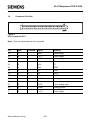
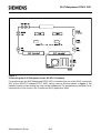
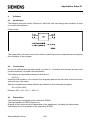
Serial Line Data Interface (SLD Interface)
The exchange of data on the SLD-Bus is based on a bidirectional, bitserial interface consisting
of three pins: SIP, DIR and SCLK.
Data is written or read out on the Serial Interface Port SIP under control of the frame
synchronization signal DIR with a period of 125 µs*). The interface clock frequency supplied at
the Slave CLock pin SCLK is 512 kHz*). The rate of the serial data stream on the SIP pin is 512
kbit/s, that is 64 bits per each 8 kHz frame*).
Starting with the rising edge of DIR, four bytes of information are transferred on the SLD-Bus
to the SICOFI, followed by four bytes from the SICOFI to the SLD-Bus. Bit 7 (MSB) is the first
bit transferred and bit 0 (LSB) is the last one of each byte.
DIR
Receive
SLD-Bus
Transmit
SICOFI
R
SICOFI
R
SIP
Channel A
Channel B
Control
Signaling
Channel A
Channel B
SIP
Channel A
Channel B
Control
Signaling
Channel A
Channel B
Control
Signaling
SIP
Linear Voice
Linear Voice
SLD-Bus
Control
Signaling
Linear Voice
Control
LIO
00
01
Signaling
10
125 µ s
LIO : Field LIO (Linear Operating Mode)
in CR 3
DIR
SCLK
SIP
Bit 00
Bit 63
Bit 62
Byte Sequence and Timing at Serial Interface Port SIP
*)
for applications with other clock rates see Appendix A
Semiconductor Group
35
ITD00636
PEB 2060
Programming
A message-orientated byte transfer is used, due to the fact that the SICOFI needs extended
control information. One control byte per frame and direction is transferred. With the
appropriate received commands, data can be written to the SICOFI or read from the SICOFI
onto the SLD-bus.
Data transfer to the SICOFI starts with a write command, followed by up to 8 bytes of data. The
SICOFI responds to a read command with the requested information, starting at the next
transmission period. If no status modification or data exchange is required a NOP byte is
transferred (see Programming Procedure).
Control Bytes
The 8-bit control bytes consist of either commands, status information or data. There are three
different classes of SICOFI commands:
NOP
NO OPERATION:
no status modification or data exchange
SOP
STATUS OPERATION:
SICOFI status setting/monitoring
COP
COEFFICIENT OPERATION:
filter coefficient setting/monitoring
The class of command is selected by Bit 2 and 3 of the control byte as shown below. Due to
the extended SICOFI feature control facilities, SOP- and COP-commands contain additional
information.
BIT
7
6
5
4
3
2
1
0
NOP
1
1
1
1
1
1
1
1
SOP
0
1
COP
X
0
X … don't care
NOP Command
If no status modification of the SICOFI or control data exchange is required, a No Operation
Byte NOP is transferred.
BIT
7
6
5
4
3
2
1
0
1
1
1
1
1
1
1
1
Semiconductor Group
36
PEB 2060
SOP Command
To modify or evaluate the SICOFI status, the contents of up to four configuration registers
CR1, CR2, CR3 and CR4 may be transferred to or from the SICOFI. This is done by a SOPCommand (Status Operation Command).
BIT
7
6
5
4
3
2
AD
R/W
PU
TR
0
1
1
0
LS EL
AD
Address
Information
AD = 0
AD = 1
A-SICOFI addressed
B-SICOFI addressed
This bit is evaluated if two SICOFIs are
connected to one SLD-port.
A SICOFI is accessed, if AD is
consistent with the level at pin SA
(see Signaling Byte, Programming Procedure).
R/W
Read/Write
Information
R/W = 0
R/W = 1
Write to SICOFI
Read from SICOFI
Enables reading from the SICOFI
or writing information to the SICOFI.
PU
Power Up/
Power Down
(see also CR3)
PU = 1
PU = 0
sets the SICOFI to power-up mode (operating)
resets the SICOFI to power-down (standby mode)
TR
Three Party
Conference
TR = 1
The received voice bytes of channel A
and channel B are added (A + B).
The result is filtered, D/A converted and
transferred to analog output VOUT (see also CR3).
LSEL
Length Select Information, identifies the number of subsequent data bytes
(see also Programming Procedure)
LSEL = 0 0 no byte following
LSEL = 1 1 CR1 is following
LSEL = 1 0 CR2 and CR1 are following
LSEL = 0 1 CR4, CR3, CR2 and CR1 are following
in this case the PU and TR bits are not overwritten.
Semiconductor Group
37
PEB 2060
CR1 Configuration Register 1
This configuration register is used for enabling/disabling the programmable digital filters (DB
... RG) and for accessing testmodes (TM1).
BIT
7
6
5
4
3
DB
RZ
RX
RR
RG
DB
Disable B-Filter
DB = 0
DB = 1
B-Filter enabled
B-Filter disabled
RZ
Restore Z-Filter
RZ = 0
RZ = 1
Z-Filter disabled
Z-Filter enabled
RX
Restore X-Filter
RX = 0
RX = 1
X-Filter disabled
X-Filter enabled
RR
Restore R-Filter
RR = 0
RR = 1
R-Filter disabled
R-Filter enabled
RG
Restore
GX-GR-Filter
RG = 0
RG = 1
GX-GR-Filter disabled
GX-GR-Filter enabled
TM1
2
1
TM1
TEST MODES
0
0
0
No test mode
0
0
1
Analog loop back via Z-filter (H (Z) = 1)1)
0
1
0
Disable highpass filter (part of bandpass BP)
0
1
1
Cut off receive path
1
0
0
Initialize data ram with 0x0000
1
1
0
Digital loop back via B-filter (H (B) = 1)2)
1
1
1
Digital loop back via PCM-register3)
Other codes are reserved for future use.
1)
2)
3)
Output of the interpolation filter I1 is set to 0.
Value of transfer function of the Z-filter is 1 (not programmable).
Output of the low pass decimation filter D2 is set to 0.
Value of transfer function of the B-filter is 1 (not programmable).
PCM in = PCM out. This testmode is also available in standby mode.
Semiconductor Group
38
0
PEB 2060
CR2 Configuration Register 2
BIT
7
6
5
4
3
2
1
0
D
C
B
A
EL
AM
µ/A
PCS
The first four bits D ... A in this register, program the four bidirectional signaling pins
SD ... SA. With two SICOFIs on one SLD-port only pin SD can be used, pin SA is always input
in this case and indicates the address of the SICOFI.
SA = 0 : A-SICOFI, SA = 1 : B-SICOFI (see also bit AD in SOP-command).
D
Signaling
Pin SD
D=0
D=1
SD is output
SD is input
C
Signaling
Pin SC
C=0
C=1
SC is output
SC is input
B
Signaling
Pin SB
B=0
B=1
SB is output
SB is input
A
Signaling
Pin SA
A=0
A=1
SA is output
SA is input
EL
Signaling
EL = 0
Expansion Logic EL = 1
No expansion logic
Expansion logic provided
Signaling expansion logic is only possible with
one SICOFI on port (see also Signaling Byte)
AM
Address Mode
Two SICOFIs on SLD port
One SICOFI on SLD port
The SICOFI access to the SLD-Bus voice
channel is controlled by AM and TR.
AM = 0
AM = 1
Receive (SLD-Bus ⇒ SICOFI)
Transmit (SICOFI ⇒ SLD-Bus)
AM
TR
SICOFI A
SICOFI B
SICOFI A
SICOFI B
0
0
channel A
channel B
channel A
channel B
0
1
channel B
channel A
channel B
channel A
1
0
channel A
------
channel A, B1)
------
1
1
channel A + B2)
------
channel A, B1)
------
µ/A
PCM-law
µ/A = 0
µ/A = 1
A-law
µ-law (µ255 PCM)
PCS
B-Filter
Coefficients
PCS = 0
PCS = 1
Programmed coefficients
Fixed coefficients
1)
2)
The SICOFI transmits the same byte in channel A and B.
Three Party Conference.
Semiconductor Group
39
PEB 2060
CR3 Configuration Register 3
BIT
7
6
5
AGX
AGX
AGR
PU
4
AGR
3
2
PU
TR
Analog Gain Control Transmit-Path
AGX = 0 0
0 dB
AGX = 0 1
6.03 dB amplification
AGX = 1 0
12.06 dB amplification
AGX = 1 1
14 dB amplification
Analog Gain Control Receive-Path
AGR = 0 0
0 dB
AGR = 0 1
6.03 dB attenuation
AGR = 1 0
12.06 dB attenuation
AGR = 1 1
14 dB attenuation
Power Up / Power Down1)
PU = 0
Power Down (standby)
PU = 1
Power Up (operating)
TR
Three Party Conference/Reverse Operating Mode (see CR2)1)
LIO
Linear Operating Mode (see Serial Interface)
LIO = 0 0
PCM mode
LIO = 0 1
Linear mode 12)
LIO = 1 0
Linear mode 2
(Change of linear mode becomes valid in the next DIR-cycle).
1)
2)
The bits PU and TR may also be overwritten by a SOP Command with LSEL ≠ 0 1
(PU and TR are part of the SOP Command).
With LSEL = 0 1, the bits PU and TR in the SOP Command are ignored.
Subsequent to a SOP/COP-read Command the control and signaling information
is transmitted instead of linear voice.
Semiconductor Group
40
1
0
LIO
PEB 2060
CR4 Configuration Register 4
BIT
7
6
5
TM3
TM3
4
3
0
0
2
1
TM4
TEST MODES
0
0
0
No test mode
0
0
1
Additional + 6 dB digital gain in transmit direction (GX)
0
1
1
Additional + 12 dB digital gain in transmit direction (GX)
1
0
0
Enable on chip tone generation1)
1
1
0
Far analog loop back2)
TM4
TEST MODES
0
0
0
No test mode
1
0
0
Digital loop back via analog port (VIN = VOUT)
Other codes are reserved for future use.
1)
2)
With the R-filter disabled a 2 kHz, 0 dBm0 sinusoidal signal is fed to the input of
the receive Lowpass Filter LP (other frequencies see Appendix B).
The output of the X-filter is fed to the input of the R-filter (8 kHz, 16 bit linear).
Semiconductor Group
41
0
PEB 2060
COP Command
BIT
7
6
AD
R/W
5
4
3
2
1
0
CO DE
With a COP Command coefficients for the programmable filters can be written to the SICOFI
coefficient ram or transmitted on the SLD-bus for verification.
AD
Address
AD = 0
A-SICOFI addressed
Information
AD = 1
B-SICOFI addressed
This bit is evaluated with two SICOFIs on one SLD-port only.
With two SICOFIs on port, a SICOFI is identified, if AD is consistent
with the level at pin SA (see Signaling Byte, Programming Procedure).
R/W
Read/Write
R/W = 0
Write to SICOFI
Information
R/W = 1
Read from SICOFI
This bit indicates whether filter coefficients are written to the SICOFI
or read from the SICOFI.
CODE
0
0
0
0
1
1
B-Filter coefficients part 1
(followed by 8 bytes of data)
0
0
1
0
1
1
B-Filter coefficients part 2
(followed by 8 bytes of data)
0
1
0
0
1
1
Z-Filter coefficients
(followed by 8 bytes of data)
0
1
1
0
0
0
B-Filter delay coefficients
(followed by 4 bytes of data)
1
0
0
0
1
1
X-Filter coefficients
(followed by 8 bytes of data)
1
0
1
0
1
1
R-Filter coefficients
(followed by 8 bytes of data)
1
1
0
0
0
0
GX- and GR-Filter coefficients*)
(followed by 4 bytes of data)
Other codes are reserved for future use.
*)
In the range – 8 dB to 8 dB gain adjustment is possible in steps ≤ 0.25 dB
Semiconductor Group
42
PEB 2060
Signaling Byte
The signaling interface of the SICOFI consists of 10 pins.
3 transmit signaling inputs: SI1, SI2 and SI3
3 receive signaling outputs: SO1, SO2 and SO3
4 bidirectional programmable signaling pins: SA, SB, SC and SD
Data present at SI1 … SI3 and possibly at some or all of SA … SD (if programmed as inputs)
are sampled and transferred serially on SIP onto the SLD-bus. Data received serially on SIP
from the SLD-Bus are latched and fed to SO1 … SO3 and possibly to some of SA … SD if
programmed as output.
The signaling field format is generally:
in receive direction:
BIT
7
6
5
4
3
2
1
0
SO1
SO2
SO3
SD
SC
SB
SA
SEL
7
6
5
4
3
2
1
0
SI1
SI2
SI3
SD
SC
SB
SA
SEL
in transmit direction:
BIT
where SEL is the signaling expansion bit if EL = 1 in CR2.
For the different cases possible, the signaling byte format at SIP is
Receive Signaling Byte
Transmit Signaling Byte
Bit
Case
7
4
3
2
1
0
7
1
SO1 SO2 SO3 X
X
X
X
X
SI1 SI2 SI3 SD SC SB SA 0
2
SO1 SO2 SO3 X
X
X
X
X
SI1 SI2 SI3 SD SC SB SA Z
3
SO1 SO2 SO3 SD SC SB SA X
SI1 SI2 SI3 0
0
0
0
0
4
SO1 SO2 SO3 SD SC SB SA X
SI1 SI2 SI3 Z
Z
Z
Z
Z
5 A-SIC
SO1 SO2 SO3 X
X
SI1 SI2 SI3 SD Z
Z
Z
Z
B-SIC
X
SO1 SO2 SO3 X
6 A-SIC
SO1 SO2 SO3 SD X
B-SIC
X
6
X
X
5
X
X
X
X
X
X
X
X
X
X
SO1 SO2 SO3 SD
Z … high impedance, X … don’t care
Semiconductor Group
43
Z
6
Z
5
Z
4
Z
3
2
1
0
SI1 SI2 SI3 SD
SI1 SI2 SI3 0
Z
Z
SI1 SI2 SI3 0
Z
Z
Z
Z
Z
Z
PEB 2060
Cases
1
One SICOFI is connected to one SLD port, EL = 0 (no signaling expansion logic provided);
SA … SD are programmed as transmit signaling inputs.
2
One SICOFI connected to one SLD port, EL = 1 (signaling expansion logic provided);
SA … SD are programmed as transmit signaling inputs.
3
One SICOFI is connected to one SLD port; EL = 0 (no signaling expansion logic provided);
SA … SD are programmed as receive signaling outputs.
4
One SICOFI is connected to one SLD port; EL = 1 (signaling expansion logic provided);
SA … SD are programmed as receive signaling outputs.
If a signaling expansion logic is provided (see case 2 and 4), the signaling bits SA … SD
which are programmed as signaling inputs or outputs can be used as additional expansion
bits in receive or transmit direction, respectively. As far as SICOFI is concerned, SIP is in
a high-impedance (Z) state or "don't care" (Y) state while these bits are transferred.
5
Two SICOFIs are connected to one SLD port; SD is programmed as transmit signaling
input.
6
Two SICOFIs are connected to one SLD port; SD is programmed as receive signaling
output.
If two SICOFIs are connected to one SLD port, no signaling expansion logic is possible.
SA is programmed as input automatically, and defines the addressed SICOFI:
SA = 0 : A-SICOFI
SA = 1 : B-SICOFI.
SB and SC are not usable with two SICOFIs on one SLD port.
Semiconductor Group
44
PEB 2060
Programming Procedure
The following table shows some control byte sequences. If the SICOFI has to be configured
completely during initialization, up to 60 bytes will be transferred.
DIR
Receive
Transmit
Receive
Transmit
Receive
Transmit
Receive
Transmit
Receive
Transmit
Receive
ITD02445
DIR
No Operation
NOP
NOP
NOP
NOP
NOP
NOP
NOP
NOP
NOP
NOP
LSEL = 00
SOP
NOP
LSEL = 11
SOP
NOP
CR1
NOP
LSEL = 10
SOP
NOP
CR2
NOP
CR1
NOP
LSEL = 01
SOP
NOP
CR4
NOP
CR3
NOP
CR2
NOP
CR1
NOP
LSEL = 00
SOP
NOP
LSEL = 11
SOP
CR1
LSEL = 10
SOP
CR2
X
CR1
LSEL = 01
SOP
CR4
X
CR3
X
CR2
X
CR1
4 Bytes
COP
NOP
DB4
NOP
DB3
NOP
DB2
NOP
DB1
NOP
8 Bytes
COP
NOP
DB8
NOP
DB7
NOP
DB1
NOP
4 Bytes
COP
DB4
X
DB3
DB1
X
CR2
X
CR1
8 Bytes
COP
DB8
X
DB7
DB1
X
CR2
X
CR1
SOP Write
SOP Read
COP Write
COP Read
X … don't care
Semiconductor Group
DB1, DB2 … DB8 … coefficient Data Byte 1 … 8
45
PEB 2060
Operating Modes
Basic Setting
Upon initial application of VDD or reseting pin RS to "1" while operating, the SICOFI enters a
basic setting mode. Basic setting means, that the SICOFI configuration registers CR1 … CR4
are initialized. All CR1 bits are set to "0" (all programmable filters are disabled except the BFilter where fixed coefficients are used, no test mode); CR2 is set to "1" (SA … SD are inputs,
signaling expansion logic is provided, one SICOFI on SLD-port, µ-law chosen and fixed BFilter coefficients used). All CR3 and CR4 bits are reset to "0" (no additional amplification or
attenuation, no linear mode, power down, no test mode). Receive signaling registers are
cleared. SIP is in high-impedance state, the analog output VOUT and the receive signaling
outputs SO1 … SO3 are forced to ground.
The serial interface is active to receive commands starting with the next 8-kHz SLD-Bus frame.
The serial interface port SIP remains in high-impedance state until CR2 has been defined.
If two SICOFIs are connected to one SLD port, both SICOFI's get the same SOP and CR2
information during initialization. The subsequent CR1 byte is assigned to the addressed
SICOFI only. If the two SICOFI's need different CR2 information, the SOP-CR2 sequence has
to be provided once again (each SICOFI knows its address now).
If any voltage is applied to any input before initial application of VDD, the SICOFI may not enter
the Basic Setting Mode. In this case it is necessary either to reset the SICOFI via the RS Pin
or to initialize the configuration registers CR1, CR2, CR3, CR4.
Standby Mode
Upon reception of a SOP command to load CR2 from the basic setting, the SICOFI enters the
standby mode (basic setting replaced by individual CR2). Being in the operating mode, the
SICOFI is reset to standby mode with a Power-Up bit PU = 0 (in CR3 or in the SOP-command
directly). The serial interface is active to receive and transmit new commands and data.
Operating Mode
From the standby mode, the operating mode is entered upon recognition of a Power-Up bit
PU = 1 (in CR3 or in the SOP-command directly).
Semiconductor Group
46
PEB 2060
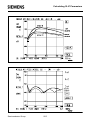
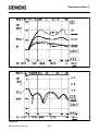
Transmission Characteristics
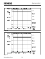
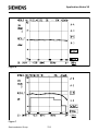
The target figures in this specification are based on the subscriber-line board requirements.
The proper adjustment of the programmable filters (transhybrid balancing: B; impedance
matching: Z; frequency-response correction: X, R) needs a complete knowledge of the
SICOFIs analog environment. Unless otherwise stated, the transmission characteristics are
guaranteed within the test condition below.
T A = 0 °C to 70 °C; V DD = 5 V ± 5 %; V SS = – 5 V ± 5 %; GNDA = GNDD = 0 V
R L > 10 kΩ; C L < 50 pF; H(Z) = H(B) = 0; H(X) = H(R) = 1;
GX = 0 to 8 dB; GR = 0 to – 8 dB; AGX = 0, 6.03, 12.06, 14 dB;
AGR = 0, – 6.03, – 12.06, – 14 dB;
f = 1000 Hz; 0 dBm0; A-law or µ-law;
A 0 dBm0 signal is equivalent to 1.5763 [1.5710] Vrms. A 3.14 [3.17] dBm0 signal is equivalent
to 2.263 Vrms which corresponds to the overload point of 3.2 V (A-law, [µ-law]).
Parameter
Symbol
Gain (either value)1)
Gain absolute (AGR = AGX = 0)
T A = 25 °C, V DD = 5 V, VSS = – 5 V
T A = 0–70 °C, V DD = 5 V ± 5%, V SS = – 5 V ± 5%
Gain absolute (AGR = 0 to 14 dB,
AGX = 0 to 14 dB)
T A = 0–70 °C; V DD = 5 V ± 5%, V SS = – 5 V ± 5%
Total harmonic distortion,
0 dBm0; f = 300 Hz to 3400 Hz
Intermodulation
Idle channel noise,
transmit, psophometric, A-law
transmit, C-message, µ-law
receive, psophometric, A-law
receive, C-message, µ-law
1)
2)
3)
min.
typ.
– 0.2
– 0.3
±
0.06 0.2
0.3
dB
dB
CT XR
CT RX
VIN = 0 V
VIN = 0 V
idle code + 0
idle code + 0
max.
– 0.4
±
0.10 0.4
dB
G
– 50
– 44
dB
– 42
– 56
dB
dB
– 85
– 85
– 80
– 80
dB
dB
– 82
8
– 67.4
17.5
– 78
12
dBm0p
dBrnc
dBm0p
dBrnc
IMD
Crosstalk
0 dBm0; f = 300 Hz to 3400 Hz
Transmit to receive
Receive to transmit
Unit
G
THD
2f1 – f22)
2f1 – f23)
Limit Values
N TP
N TC
N RP
N RC
R L = 300 Ω causes an additional attenuation in the range between – 0.1 to 0 dB.
Equal input levels in the range between – 4 dBm0 and – 21 dBm0; different frequencies in the range
between 300 Hz and 3400 Hz.
Input level – 9 dBm0, frequency range 300 Hz to 3400 Hz and – 23 dBm0, 50 Hz.
Semiconductor Group
47
PEB 2060
Attenuation Distortion
Attenuation deviations stay within the limits in the figures below.
ITD00637
Attenuation
2.0
dB
1.5
1.0
0.650
0.5
0.125
0
-0.125
-0.5
3.4
-1.0
5 6 7 8 9 10 -1
2
3
4
5 6 7 8 9 10 0
Receive: Reference frequency 1 kHz, input signal level 0 dBm0
Transmit: Reference frequency 1 kHz, input signal level 0 dBm0
Semiconductor Group
48
2
f
kHz
4
PEB 2060
Group Delay
Maximum delays for operating the SICOFI with H(B) = H(Z) = 0 and H(R) = H(X) = 1, including
delay through A/D- and D/A converters. Specific filter programming may cause additional
group delays.
Group delay deviations stay within the limits in the figures below.
Group Delay Absolute Values: Input signal level 0 dBm0
Parameter
Limit Values
Symbol
min.
typ.
Unit
Test Condition
max.
Transmit Delay
D XA
300
µs
f = 1.4 kHz
Receive Delay
D RA
240
µs
f = 300 Hz
ITD00639
500
µs
t 400
300
250
200
100
70
0.7
0
0
0.5
2.8
1.0
1.5
2.0
2.5
3.1
3.0 kHz 3.5
f
Group Delay Distortion: Input signal level 0 dBm0, reference frequency = 1.4 kHz
Semiconductor Group
49
PEB 2060
Out-of-Band Signals at Analog Input
With an out-of-band sine wave signal with frequency f and level A applied to the analog input,
the level of any resulting frequency component at the digital output will stay at least X dB below
level A.
ITD00640
dB
Attenuation
0
-6
-12
6
-18
10 -2
5
10 -1
5
10
18
10 1
5 kHz 10 2
f
ITD00641
40
Attenuation
dB
30
20
10
0.06
0
10 -2
5
4.6
10 -1
5
10 1
5 kHz 10 2
f
Out-of-Band Signals at Analog Output
With a 0 dBm0 sine wave of frequency f applied to the digital input, the level of any resulting
out-of-band signal at the analog output will stay at least X dB below a 0 dBm0, 1 kHz sine wave
reference signal at the analog output.
ITD00642
50
dB
Attenuation
40
30
20
15
10
4.6
0
10 -2
5
10 -1
5
10 1
5 kHz 10 2
f
Semiconductor Group
50
PEB 2060
Gain Tracking (Receive and Transmit)
The gain deviations stay within the limits in the figures below
ITD00643
1.0
∆G
dB
0.5
0.4
0.2
0.25
0
0.2
-0.5
0.4
0.25
-55
-1.0
-70
-60
-35
-50
-40
-30
-20
-10
0 dBm0 10
Input Level
Gain Tracking: Measured with noise signal according to CCITT recommendations, reference
level is – 10 dBm0, AGX = AGR = 0
ITD00644
2
∆G
dB
1.4
1
0
0.5
0.2
-0.2
-0.5
0.25
-0.25
-1
-1.4
-55
-2
-70
-60
3
-50
-40
-30
-20
-10
0 dBm0 10
Input Level
Gain Tracking: Measured with sine wave in the range 700 to 1100 Hz, reference level is –
10 dBm0, AGX = AGR = 0
Semiconductor Group
51
PEB 2060
Total Distortion
The signal-to-distortion ratio exceeds the limits in the following figures.
ITD00645
40
S/D
dB
36.0
30
29.7
36.7
34.3
28.4
20
14.7
10
-55
0
-60
-34
-50
-40
-27 -24
-6 -3
-30
-20
Input Level
-10 dBm0 0
Receive: Measured with noise signal according to CCITT recommendations
ITD00646
40
S/D
dB
30
36.3
35.4
33.3
27.4
28.7
20
13.7
10
-55
0
-60
-34
-50
-40
-27 -24
-30
-6 -3
-20
-10 dBm0 0
Input Level
Transmit: Measured with noise signal according to CCITT recommendations
Semiconductor Group
52
PEB 2060
The signal to distortion ratio exceeds the limits in the following figures.
ITD00647
40
S/D
dB
35.5
30
31.0
27.0
24.5
36.4
µ - LAW
29.5
A - LAW
20
10
-28
-45
0
-60
-50
-40
-30
-20
-10 dBm0 0
Input Level
Receive & Transmit: Measured with sine wave in the range 700 to 1100 Hz excluding
submultiples of 8 kHz
Signal to Total Distortion CCITT Noise Signal Digital-Digital (A-law and µ-law)
Parameter
Total Distortion
Digital Loop Back via B-Filter or Digital Loop
Back via Analog port
Semiconductor Group
53
Input Level Unit
min.
Unit
0
– 30
– 40
– 45
31
31
25
20
dB
dB
dB
dB
dBm0
dBm0
dBm0
dBm0
PEB 2060
Transhybrid Loss
The quality of transhybrid-balancing is very sensitive to deviations in gain and group delay –
deviations inherent to the SICOFI A/D- and D/A-converters as well as to all external
components used on a line card (SLIC, OP's etc.)
The SICOFI transhybrid loss is measured in the following way: A sine wave signal with level
0 dBm0 and a frequency in the range of 300 – 3400 Hz is applied to the digital input. The
resulting analog output signal at pin VOUT is directly connected to VIN, e.g. with the SICOFI
testmode "Digital Loop Back via Analog Port" (see CR4). The programmable filters R, GR, X,
GX and Z are disabled, the balancing filter B is enabled with coefficients optimized for this
configuration (VOUT = VIN).
The resulting echo measured at the digital output is at least X dB below the level of the digital
input signal as shown in the table below.
B-filter coefficients recommended for transhybrid loss measurement with V OUT = V IN
COP-Write
B-filter part 1
B-filter part 2
B-filter delay
(83)
(8B)
(98)
Parameter
Coefficients
FD
00
19
Symbol
29
AF
19
FB
62
11
Limit Values
min.
typ.
38
2B
19
A1
CF
A0
D1
3C
CA
Unit
Test Condition
42
A4
Transhybrid loss at 500 Hz
Transhybrid loss at 2500 Hz
Transhybrid loss at 3000 Hz
THL500
THL2500
THL3000
33
29
27
45
40
35
dB
dB
dB
T A = 25 °C,
V DD = 5 V, V SS = – 5 V,
AGR = AGX = 0 dB
Transhybrid loss at 500 Hz
Transhybrid loss at 2500 Hz
Transhybrid loss at 3000 Hz
THL500
THL2500
THL3000
29
27
25
40
35
30
dB
dB
dB
T A = 0 to 70 °C,
V DD = 5 V ± 5 %,
V SS = 5 V ± 5 %,
AGR = AGX = 0 dB
Transhybrid loss at 500 Hz
Transhybrid loss at 2500 Hz
Transhybrid loss at 3000 Hz
THL500
THL2500
THL3000
27
25
23
40
35
30
dB
dB
dB
T A = 0 to 70 °C,
V DD = 5 V ± 5 %,
V SS = – 5 V ± 5 %,
AGR = AGX = 6.03,
12.06,
14.00 dB
Semiconductor Group
54
PEB 2060
Absolute Maximum Ratings
Parameter
Symbol
Limit Values
Unit
min.
max.
V DD referred to GNDD
– 0.3
5.5
V
V SS referred to GNDD
– 5.5
0.3
V
GNDA to GNDD
– 0.6
0.6
V
Analog input and output voltage
referred to V DD = 5 V, V SS = – 5 V
referred to V SS = – 5 V, V DD = 5 V
V IN
V IN
– 10.3
– 0.3
0.3
10.3
V
V
All digital input voltages
referred to GNDD = 0 V, V DD = 5 V
referred to V DD = 5 V, GNDD = 0 V
V IN
V IN
– 0.3
– 5.3
5.3
0.3
V
V
10
mA
DC input and output current at any input
or output pin
I DC
Storage temperature
T stg
– 60
125
°C
Ambient temperature under bias
TA
– 10
80
°C
Power dissipation
PD
1
W
Operating Range
T A = 0 to 70 °C; V DD = 5 V ± 5%; V SS = – 5 V ± 5%; GNDD = 0 V; GNDA = 0 V
Parameter
Symbol
Limit Values
min.
V DD supply current
stand by
operating
I DD
V SS supply current
stand by
operating
I SS
Power supply rejection
(of either supply/direction)
PSRR
Power dissipation stand by
Power dissipation operating
P Ds
P Do
Semiconductor Group
30
typ.
max.
2.1
8
4
12
mA
mA
1.7
5
3
8
mA
mA
44
20
70
55
Unit Test Condition
dB
37
105
mW
mW
1 kHz
80 mVrms ripple
PEB 2060
Electrical Characteristics
Digital Interface
T A = 0 to 70 °C; V DD = 5 V ± 5 %; V SS = – 5 V ± 5%; GNDD = 0 V; GNDA = 0 V
Parameter
Symbol
Limit Values
min.
max.
0.8
L-input voltage
V IL
– 0.3
H-input voltage
V IH
2.0
L-output voltage
V OL
H-output voltage
V OH
Input leakage current
I IL
Unit
Test Condition
V
V
0.45
2.4
±
1
V
I 0 = – 2 mA
V
I 0 = 400 µA
µA
– 0.3 ≤ V IN ≤ V DD
Analog Interface
T A = 0 to 70 °C; V DD = 5 V ± 5%; V SS = – 5 V ± 5%; GNDD = 0 V; GNDA = 0 V
Parameter
Symbol
Limit Values
min.
Unit
max.
Analog input resistance
RI
Analog output resistance
RO
10
Ω
Input offset voltage
V IO
±
50
mV
Output offset voltage
V OO
±
50
mV
Input voltage range
V IR
±
3.2
V
Output voltage range
V OR
Semiconductor Group
10
±
Test Condition
MΩ
3.1
56
V
R L ≥ 300 Ω; C L ≤ 50 pF
PEB 2060
t SCLK
90%
SCLK
10%
t DIRxS
t DIRxH
t DIR
DIR
t SCLK
2
t DINxS
t SCLK
2
t DINxH
SIP
Data IN
t dOUT
t dDHZ
High
Imp.
SIP
Data OUT
ITT00649
SIP Interface Timing (SLD-Bus)
Switching Characteristics
Parameter
Symbol
Limit Values
min.
Period SCLK
t SCLK
Duty cycle
typ.
Unit
max.
1/512 kHz
20
50
80
%
µs
Period DIR
t DIR
DIR setup time
t DIR × S
20
DIR hold time
t DIR × H
250
ns
SIP data in setup time
t DIN × S
20
ns
SIP data in hold time
t DIN × H
100
ns
SIP data out delay
t dDOUT
150
250
ns
SIP data out high impedance
delay vs. SCLK
t dDHZ
50
70
ns
Semiconductor Group
57
125
0
– 80
ns
PEB 2060
SCLK
90%
10%
SIP
Data IN
Last Signaling
Bit IN
t dSIG OUT
SIG OUT
SIP
Data IN
Last Control
Bit IN
t dSIGZ
SIG OUT
t SIG INxS
t SIG INxH
SIG IN
SIP
Data IN
Last Control
Bit OUT
First Signaling
Bit OUT
ITD02446
Signaling Interface Timing
Switching Characteristics
Parameter
Symbol
Limit Values
min.
typ.
Unit
max.
Delay signaling out vs. SCLK1)
t dSIGOUT
250
350
ns
Delay signaling high impedance
vs. SCLK
t dSIGZ
150
200
ns
SIG in setup time2)
t SIGIN × S
50
ns
SIG in hold time2)
t SIGIN × H
100
ns
Reset pulse width3)
t RES
500
ns
1)
2)
3)
Pins SO1 … SO3; Pins SA … SD as output
Pins SI1 … SI3; Pins SA … SD as input
SICOFI is ready to accept SOP/COP commands in the next DIR Cycle.
Spikes shorter than 244 ns will be ignored.
Semiconductor Group
58
PEB 2060
Appendix A
Specific Interface Types
The SICOFI can be used with three different SLD-bus type interfaces. A specific interface type
is selected with three pins: TEST, SI3 and PLL.
TEST
SI3
PLL
0
X
X
DIR
f = 8 kHz
SCLK
f = 512 kHz
MCLK
f = 4096 kHz
SIP Data
f = 256 kHz
ITD00651
1) SLD-Bus Interface1)
*)
TEST
SI3*)
PLL
1
0
0
SI3 cannot be used
as Signaling Pin
DIR
f / 512 kHz
SCLK
f
MCLK
f
SIP Data
f / 16 kHz
ITD00652
2) SLD-Bus Interface with Variable Clock Frequencies 2)
1)
2)
4096-kHz Masterclock MCLK is generated from 512-kHz SCLK by on chip PLL
Maximum MCLK-frequency = 8 MHz
Semiconductor Group
59
PEB 2060
*)
TEST
SI3*)
PLL
1
0
1
SI3 cannot be used
as Signaling Pin
DIR
f / 512 kHz
SCLK
f
MCLK
f
SIP Data
f / 2 kHz
ITD00653
3) Burst Mode Interface1)
1)
Maximum MCLK-frequency = 8 MHz
Semiconductor Group
60
PEB 2060
In burst-mode 8- or 16-bit bursts are received or transmitted, depending on the linear mode
selected (see field LIO in CR3).
DIR
Voice A
Voice B
Control
Signaling
Voice A
Voice B
Control
Signaling
SIP
Field LIO = 00
A
B
C
S
A
B
C
S
A
A
B
C
S
A
B
MSB
LSB
A
SIP
Field LIO = 01
SIP
Field LIO = 10
MSB + LSB
C+S
MSB + LSB
C+S
MSB + LSB
ITD00654
Detail A
DIR
SCLK
SIP
Field LIO = 00
7
6
5
4
3
2
1
0
4
3
2
1
0
15 14 13 12 11 10 9
8
Voice A
SIP
Field LIO = 01
7
6
5
Voice A
SIP
Field LIO = 10
7
Detail A
voice A
C … control
voice B
S … signaling
bit 15-8 of linear in- or output
bit 7-0 of linear in- or output
Semiconductor Group
5
4
3
2
1
0
ITD00655
Linear Voice
A…
B…
MSB …
LSB …
6
61
PEB 2060
Appendix B
On Chip Tone Generation
By setting field TM3 in CR4 to ’100’ the on-chip tone generator is activated with a fixed
frequency of 2 kHz. The frequency fTONE may be programmed via the R-filter coefficients (Rfilter enabled) in the range of 0 to 4 kHz. The gain may be adjusted with the programmable GRfilter.
The trapezoidal tone generation algorithm used, provides for a harmonic distortion better than
27 dB.
Calculation of the R-filter Coefficients:
fTONE : = 8192 × INC/f MCLK with f MCLK, f TONE [kHz]
INC : = SR1 × 2–EXPR1 × (1 + SR2 × 2–EXPR2 × (1 + SR3 × 2–EXPR3 × (…(…(1 + SR9 × 2–EXPR9)…))
S … SIGN, EXP … EXPONENT
1
+
R9
+
R8
+
R7
+
R6
+
R5
+
R4
+
R3
INC
+
R2
R1
ITD00656
A1 : = INC
FOR i : = 1 TO 9 DO
FIND Si, EXPi: FOR (Ai – Si × 2–EXPi) = MIN; Si ∈ (– 1, 1), EXPi ∈ (0 … 7)
A i +1 : = (Ai / Si × 2–EXPi) –1
R i : = [ (– Si +1)/2), BIN(EXPi) ] (to be transferred to the SICOFI)
NEXT i
Programming Byte Sequence for Selected Frequencies
Coefficients
COP write*)
Frequency Hz
2000 1000 800
697
770
852
941
1209 1336 1477 1633
2B/AB 2B/AB 2B/AB 2B/AB 2B/AB 2B/AB 2B/AB 2B/AB 2B/AB 2B/AB 2B/AB
X
X
00
00
00
00
00
00
00
00
00
00
00
X
X
00
00
00
00
00
00
00
00
00
00
00
X
X
00
00
00
00
00
00
00
00
00
00
00
R1
X
00
10
10
20
10
10
10
10
10
10
00
R3
R2
8F
8F
AA
A1
CA
3B
CC
B2
22
D1
1B
R5
R4
8F
8F
AA
2B
32
C1
BB
22
A1
C1
5C
R7
R6
8F
8F
AA
4B
2D
BB
12
5F
5F
BB
CA
R9
R8
8F
8F
AA
B1
B3
12
DA
8F
1B
12
13
X don’t care
*) 2B for SICOFI A, AB for SICOFI B.
Semiconductor Group
62
Dual Channel Codec Filter (SICOFI®-2)
PEB 2260
PEF 2260
Features
CMOS IC
●
Dual channel single chip codec and filter
●
Band limitation according to all CCITT
and AT&T recommendations
●
Digital signal processing techniques
●
PCM encoded digital voice transmission
(A-law or µ-law)
●
Programmable digital filters for
– impedance matching
– transhybrid balancing
– gain
– frequency response correction
●
Two digital Interfaces
– three pin serial SLD Interface
(eg. to PEB 2050/52)
– four pin serial IOM®-2 Interface with two
different clock-frequencies and time-slot
assignment (e.g. to PEB 2055/56)
P-LCC-28-R
Programmable signaling interface
to peripherals (e.g. SLIC)
● High performance A/D and D/A conversion
● Programmable analog gain adjustment
● Advanced test capabilities
– three digital loop back modes
– two analog loop back modes
– two programmable tone generators
●
●
●
●
●
●
●
No trimming or adjustments
No external components
Advanced low power 2µCMOS
technology
Power supply + / – 5 V
Meets or exceeds CCITT and LSSGR
recommendations
Two types are available:
– PEB 2260 with standard temperature
range 0...70oC
– PEF 2260 with extended temperature
range -40...85oC
Type
Version
Ordering Code
Package
PEB 2260-N
V 2.0
Q67100-H6191
P-LCC-28-R (SMD)
PEF 2260-N
V 2.0
Q67100-H6261
P-LCC-28-R (SMD)
Semiconductor Group
63
03.92
PEB 2260
PEF 2260
General Description
The Dual Channel Codec Filter PEB 2260 (SICOFI®-2) is a fully integrated PCM codec and
filter fabricated in low power 2µCMOS technology for applications in digital communication
systems. Based on an advanced digital filter concept, the PEB 2260 provides excellent
transmission performance and high flexibility. The digital signal processing approach includes
attractive programmable features such as transhybrid balancing, impedance matching, gain
and frequency response correction.
Pin Configuration for IOM®-2 Mode
(top view)
Pin Configuration for SLD Mode
(top view)
Semiconductor Group
64
PEB 2260
PEF 2260
Pin Definitions and Functions for SLD Interface Mode
Pin No. Symbol
Input (I)
Output (O)
Function
22
V DD
I
+ 5 V power supply
8
V SS
I
– 5 V power supply
24
GNDD
I
Ground digital.
Not internally connected to GNDA or GNDB.
All digital signals are referred to this pin
1
GNDA
I
Ground analog channel A.
Not internally connected to GNDD or GNDB.
All channel A analog signals are referred to this pin
15
GNDB
I
Ground analog channel B.
Not internally connected to GNDD or GNDA.
All channel B analog signals are referred to this pin
27
VINA
I
Channel A analog voice input
3
VOUTA
O
Channel A analog voice output
17
VINB
I
Channel B analog voice input
13
VOUTB
O
Channel B analog voice output
25
MODE
I
Operating mode selection, SLD or IOM-2 Interface:
connected to '0' for SLD interface mode
21
SCLK
I
Slave clock, 512 kHz
20
DIR
I
Direction Signal, 8-kHz frame synchronisation
19
SIP
I/O
Serial interface port, bidirectional serial data port
23
RS
I
Reset input, RS forces the SICOFI-2 to basic setting
mode
2
SI1A
I
28
SI2A
I
26
SI3A
I
14
SI1B
I
16
SI2B
I
18
SI3B
I
Semiconductor Group
Signaling inputs: data present at SI1A ... SI3B are
sampled and transmitted via the serial interface
65
PEB 2260
PEF 2260
Pin Definitions and Functions for SLD Interface Mode (continued)
Pin No. Symbol
Input (I)
Output (O)
5
SO1A
O
6
SO2A
O
7
SO3A
O
11
SO1B
O
10
SO2B
O
9
SO3B
O
4
SBA
I/O
12
SBB
I/O
Function
Signaling outputs: data received via the serial interface are
latched and fed to SO1A ... SO3B
Bidirectional signaling pins: SBA, SBB pins may be
programmed as input or output individually with
adequate SICOFI-2 status settings
Pin Definitions and Functions for IOM®2 Interface Mode
Pin No. Symbol
Input (I)
Output (O)
Function
22
V DD
I
+ 5 V power supply
8
V SS
I
– 5 V power supply
24
GNDD
I
Ground digital.
Not internally connected to GNDA or GNDB.
All digital signals are referred to this pin
1
GNDA
I
Ground analog channel A.
Not internally connected to GNDD or GNDB.
All channel A analog signals are referred to this pin
15
GNDB
I
Ground analog channel B.
Not internally connected to GNDD or GNDA.
All channel B analog signals are referred to this pin
27
VINA
I
Channel A analog voice input
3
VOUTA
O
Channel A analog voice output
17
VINB
I
Channel B analog voice input
13
VOUTB
O
Channel B analog voice output
25
MODE
I
Operating mode selection, SLD or IOM-2 Interface:
connected to '1' for IOM-2 interface mode
Semiconductor Group
66
PEB 2260
PEF 2260
Pin Definitions and Functions for IOM®2 Interface Mode (continued)
Pin No. Symbol
Input (I)
Output (O)
Function
21
DCL
I
Data clock, 512 kHz or 4096 kHz
20
FSC
I
Frame synchronisation clock, 8 kHz
19
DU
O
Data upstream
18
DD
I
Data downstream
23
RS
I
Reset input, RS forces the SICOFI-2 to basic setting
mode
28
I1A
I
16
I1B
I
Indication inputs: data present at I1A ... I1B are sampled
and transmitted via the serial interface
5
C1A
O
6
C2A
O
26
C3A
O
11
C1B
O
10
C2B
O
2
CI1A
I/O
4
CI2A
I/O
14
CI1B
I/O
12
CI2B
I/O
7
TS1
I
9
TS2
I
Semiconductor Group
Command outputs: data received via the serial interface
are latched and fed to C1A ... C3A and C1B ... C2B
Bidirectional command/indication pins: CI1A ... CI2B may
be programmed as input or output individually with
adequate SICOFI-2 status settings
Time-slot selection pins 1 ... 2 with ternary logic
67
PEB 2260
PEF 2260
SICOFI®-2 Principles
The SICOFI-2 codec filter solution is a highly digital approach utilizing the advantages of digital
signal processing such as excellent performance, high flexibility, easy testing, no sensitivity to
fabrication and temperature variations, no problems with crosstalk and power supply rejection.
VIN
AGX
PREFI
A/D
D1
+
D2
GX
LPX
HP
X
Comp
R
Exp
PCMOUT
Transmit
Z
TG
1, 2
B
Receive
VOUT
POFI
AGR
D/A
I2
+
I1
GR
LPR
PCMIN
ITS02447
SICOFI®-2 Signal Flow Graph (for either channel)
Transmit Direction
The analog input signal is A/D converted, digitally filtered and transmitted PCM-encoded.
Antialiasing is done with a 2nd order Sallen-Key prefilter (PREFI). The A/D Converter (ADC) is
a modified slopeadaptive interpolative sigma-delta modulator with a sampling rate of 128 kHz.
Digital downsampling to 8 kHz is done by subsequent decimation filters D1 and D2 together
with the transmit PCM lowpass filter (LPX).
Receive Direction
The digital input signal is received PCM-encoded, digitally filtered and D/A converted to
generate the analog output signal. Digital interpolation up to 128 kHz is done by the receive
PCM lowpass filter (LPR) and the interpolation filters I1 and I2. The D/A Converter (DAC)
output is fed to the 2nd order Sallen-Key postfilter (POFI).
Programmable Functions
The high flexibility of the SICOFI-2 is based on a variety of user programmable filters, which
are analog gain adjustment AGR and AGX, digital gain adjustment GR and GX, frequency
response adjustment R and X, impedance matching filter Z and the transhybrid balancing
filter B.
Semiconductor Group
68
PEB 2260
PEF 2260
SLIC-Interface
DIR/FSC
VIN A
PREFI
ADC
SCL/DCL
SLD/
R
Channel A
VOUT A
SIP/DU
IOM -2
Interface
POFI
DD
DAC
DSP
VIN B
PREFI
ADC
Coeff.
RAM
Channel B
VOUT B
POFI
DAC
ITB00659
SICOFI®-2 Block Diagram
The SICOFI-2 bridges the gap between analog and digital voice signal transmission in modern
telecommunication systems.
High performance oversampling Analog-to-Digital Converters (ADC) and Digital-to-Analog
Converters (DAC) provide the conversion accuracy required. Analog antialiasing prefilters
(PREFI) and smoothing postfilters (POFI) are included. The dedicated on chip Digital Signal
Processor (DSP) handles all the algorithms necessary, e.g. PCM bandpass filtering, sample
rate conversion and PCM companding. The SLD or IOM-2 Interface handles digital voice
transmission, SICOFI-2 feature control and access to the SICOFI-2 signaling pins. Specific
filter programming is done by downloading coefficients to the coefficient ram (CRAM).
Semiconductor Group
69
PEB 2260
PEF 2260
SICOFI®-2 Digital Interfaces
The SICOFI-2 digital interface section consists of a serial interface bus which can be
configured to be compatible to SLD or the IOM-2 standard (with two different data clock
frequencies), and a powerful signaling interface.
Selecting between the IOM-2 and SLD interfacing mode is simply performed by strapping the
MODE pin.
MODE = ’0’ : SLD Interface
MODE = ’1’ : IOM-2 Interface
For better understanding, pin names are quoted with their interface specific name. E.g. pin
SIP/DU: SIP for SLD interface mode, DU for IOM-2 interface mode.
SLD Interface
The SLD serial interface consists of a bidirectional pin SIP, a data clock input SCLK, and a
synchronization input DIR. Data bits are loaded or read out by the serial interface pin SIP. Bits
are clocked in at the falling edge and clocked out at the rising edge of the slave clock pin SCLK
(512 kHz). DIR and SCLK inputs must be phase locked. A SLD frame lasts 125 µs and
consists of 32 bits transferred to the SICOFI-2 followed by 32 bits transferred from the SICOFI2 to the SLD bus. The SLD interface thus provides a full duplex 256 kbit/s communication
channel. This channel is subdivided in two 64 kbit/s voice/data channels, a 64 kbit/s feature
control channel and an other 64 kbit/s signaling channel per direction. Bytes in all channels are
serialized MSB first.
DIR
Receive
SIP
SICOFI R - 2
SLD - Bus
SCLK
Channel A
Transmit
Channel B
Control
SICOFI R - 2
Signaling
Channel A
125 µ s
DIR
SCLK
SIP
Bit 00
Bit 63
Bit 62
ITD02448
Semiconductor Group
70
Channel B
SLD - Bus
Control
Signaling
PEB 2260
PEF 2260
IOM®-2 Interface
The IOM-2 interface consists of two data lines and two clock lines. DU (data upstream) carries
data from the SICOFI-2 to a master device. DD (data downstream) carries data from the
master device to the SICOFI-2. A 8 kHz FSC (frame synchronization clock) signal as well as
a 512 kHz or 4096 kHz DCL (data clock) signal is supplied. The SICOFI-2 implements all
functions for analogue devices as described in the IOM-2 specification.
125 µ s
FSC
DCL
512 kHz
DD
B1
B2
MONITOR Data
C/I 6:1
MM
R X
DU
B1
B2
MONITOR Data
C/I 6:1
MM
R X
ITD02449
Detail A
IOM®-2 Interface, DCL = 512 kHz (one channel per frame)
125 µ s
FSC
DCL
4096 kHz
DD
CH0
CH1
CH2
CH3
CH4
CH5
CH6
CH7
DU
CH0
CH1
CH2
CH3
CH4
CH5
CH6
CH7
ITD02450
Detail A
Detail B
IOM®-2 Interface, DCL = 4096 kHz (eight channels per frame)
Semiconductor Group
71
PEB 2260
PEF 2260
FSC
DCL
DD/DU
Bit n
Bit 0
Bit 1
ITD02451
Detail A
DD
B1
B2
MONITOR Data
C/I 6:1
MR MX
DU
B1
B2
MONITOR Data
C/I 6:1
MR MX
ITD02452
Detail B
Semiconductor Group
72
PEB 2260
PEF 2260
With a DCL frequency of 4096 kHz assignment of 8 time slots is possible. The IOM-2 operating
mode and time-slot selection is set completely by pin-strapping of two pins TS1 and TS2,
which work with ternary logic (– 5 V [N], 0 V [0] and + 5 V [P]).
TS2
TS1
IoM-2 Operating Mode
N
N
IOM-2, DCL = 512 kHz
0
0
IOM-2, DCL = 4096 kHz, time slot 0
N
0
IOM-2, DCL = 4096 kHz, time slot 1
0
P
IOM-2, DCL = 4096 kHz, time slot 2
N
P
IOM-2, DCL = 4096 kHz, time slot 3
P
0
IOM-2, DCL = 4096 kHz, time slot 4
0
N
IOM-2, DCL = 4096 kHz, time slot 5
P
P
IOM-2, DCL = 4096 kHz, time slot 6
P
N
IOM-2, DCL = 4096 kHz, time slot 7
IOM®-2 MONITOR Channel Data Structure
The MONITOR channel is used for the transfer of maintenance information between two
functional blocks. By use of two MONITOR control bits (MR and MX) per direction, the data
are transferred in a complete handshake procedure.
The messages transmitted in the MONITOR channel may have different kinds of data
structures. Therefore, the first byte of the message is used to indicate the structure of the
following data.
Messages to and from the SICOFI-2 are started with the following byte:
BIT
7
6
5
4
3
2
1
0
1
0
0
0
0
0
0
1
Thus providing information for two analog lines, the SICOFI-2 is one device on one IOM-2
channel. MONITOR data for a specific analog channel is selected by the SICOFI-2 specific
command following.
For more details on IOM-2 MONITOR channel data structure, and an IOM-2 specific
identification command see Appendix B.
Semiconductor Group
73
PEB 2260
PEF 2260
Programming
A message oriented byte transfer is used, due to the fact that the SICOFI-2 needs extended
control information. With the appropriate commands, data can be written to the SICOFI-2 or
read from the SICOFI-2 via the SLD or via the IOM-2 interface monitor channel.
Data transfer to the SICOFI-2 starts with a write command, followed by up to 8 bytes of data.
The SICOFI-2 responds to a read command with the requested information, that is up to 8
bytes of data. (see Programming procedure).
The same command structure is used both in SLD and IOM-2 interface mode. If the SICOFI2 is operating in IOM-2 interface mode, any new command sequence starts with a SICOFI-2
specific address-byte. The following command is the same in SLD and IOM-2 mode. If the
command requests an answer, in SLD mode the SICOFI-2 will start immediately (next
transmission period) with the requested data. In IOM-2 mode the SICOFI-2 specific address
byte will be sent first, followed by the requested data.
Attention: In IOM-2 mode, each byte on the monitor channel, is sent twice at least.
Example for a programming sequence in SLD and IOM-2 interface mode:
SLD Interface
Receive
SOP-Write
CR2
CR1
SOP-Read
Semiconductor Group
Transmit
CR2
CR1
IOM-2 Interface
Receive
Transmit
Address
SOP-Write
CR2
CR1
SOP-Read
Address
CR2
CR1
74
PEB 2260
PEF 2260
Control Bytes
The 8-bit control bytes consist of either commands, status information or data. There are three
different classes of SICOFI-2 commands:
NOP
NO OPERATION:
no status modification or data exchange
SOP
STATUS OPERATION:
SICOFI-2 status setting/monitoring
COP
COEFFICIENT OPERATION:
filter coefficient setting/monitoring
The class of command is selected by bit 3 and 2 of the control byte as shown below.
BIT
7
6
5
4
3
2
NOP
1
1
SOP
0
1
COP
X
0
1
0
X … don't care
Due to the extended SICOFI-2 feature control facilities, SOP and COP commands contain
additional information for programming and verifying the SICOFI-2.
Programmable Devices
3 configuration registers per channel:
1 coefficient ram per channel:
1 common configuration register:
CR1, CR2, CR3
CRAM
CR4 is only available in IOM-2 mode
the contents of CR4 is valid for both channels
To obtain more clarity, bit fields containing different informations for SLD and IOM-2 interface
are high lighted in subsequent chapters.
Semiconductor Group
75
PEB 2260
PEF 2260
NOP Command
If no status modification of the SICOFI-2 is required, a no operation byte NOP may be
transferred.
NOP receive, not useful in IOM-2 interface mode
BIT
7
6
5
4
3
2
1
0
X
X
X
X
1
1
X
X
3
2
1
0
NOP transmit, only available in SLD interface mode
BIT
7
6
5
4
1
1
PDA
PDB
VERSION
PDA
PDA = 1
PDA = 0
if channel A is in power-down mode
if channel A is in power-up mode
PDB
PDB = 1
PDB = 0
if channel B is in power-down mode
if channel B is in power-up mode
VERSION
Four bit SICOFI-2 version identification
VERSION = 1111 for PEB2260 V1.X, V2.0
Semiconductor Group
76
PEB 2260
PEF 2260
SOP Command
To modify or evaluate the SICOFI-2 status, the contents of up to three (four) configuration
registers CR1, CR2, CR3 (and CR4) may be transferred to or from the SICOFI-2. This is done
by a SOP-Command (status operation command). In SLD interface mode three configuration
registers per channel are accessible. If the SICOFI-2 is operating with IOM-2 interface an
additional fourth configuration register (CR4) can be written or read.
BIT
7
6
5
4
3
2
AD
R/W
PU
RST
0
1
1
0
LS EL
AD
Address Information
AD = 0
channel A is addressed with this command
AD = 1
channel B is addressed with this command
R/W
Read/Write Information: Enables reading from the SICOFI-2 or writing
information to the SICOFI-2.
R/W = 0
Write to SICOFI-2
R/W = 1
Read from SICOFI-2
PU
Power Up/Power Down
PU = 1
sets the assigned channel (see bit AD) of SICOFI-2
to power-up mode (operating)
PU = 0
resets the assigned channel of SICOFI-2 to power-down
(standby mode)
RST
Reset SICOFI-2
RST = 1
LSEL
⇒
⇒
*)
forces SICOFI-2 to enter the Basic Setting Mode
(see Operating Modes).
Length select information (see also Programming Procedure)
This two bit field identifies the number of subsequent data bytes
LSEL = 0 0
no byte following
LSEL = 1 1
CR1 is following
LSEL = 1 0
CR2 and CR1 are following
LSEL = 0 1
CR3, CR2 and CR1 are following in SLD interface mode
CR4*), CR3, CR2, CR1 are following in IOM-2 interface mode
Commands concerning CR4 are independent of bit AD in SOP command.
Semiconductor Group
77
PEB 2260
PEF 2260
CR1 Configuration Register 1
Configuration register CR1 defines the basic SICOFI-2 settings, which are:
enabling/disabling the programmable digital filters, programming of signaling pins, and
selection of the PCM companding characteristics.
BIT
B
Z
X
R
GR
GX
SB/C3A
⇒
⇒
SB/C3A
⇒
⇒
LAW
*)
7
6
5
4
3
2
1
0
B
Z
X
R
GX
GR
SB/C3A
LAW
Enable B - filter
B = 0
B = 1
B - filter disabled, H(B) = 0
B - filter enabled
Enable Z - filter
Z = 0
Z = 1
Z - filter disabled, H(Z) = 0
Z - filter enabled
Enable X - filter
X = 0
X = 1
X - filter disabled, H(X) = 1
X - filter enabled
Enable R - filter
R = 0
R = 1
R - filter disabled, H(R) = 1
R - filter enabled
Enable GR - filter
GR = 0
GR = 1
GR - filter disabled, H(GR) = 1
GR - filter enabled
Enable GX - filter
GX = 0
GX = 1
GX - filter disabled, H(GX) = 1
GX - filter enabled
SLD Interface mode: program bidirectional signaling pin SBA or SBB
SB = 0
programmable signaling pin SBx is input
SB = 1
programmable signaling pin SBx is output
IOM-2 interface mode: operation mode of pin C3A*)
C3A = 0
pin C3A is programmed as command output
C3A = 1
pin C3A is detector select output (see CR4)
PCM - Law selection
LAW = 0
LAW = 1
A - law
µ - law (µ255 PCM)
Setting bit C3A to ’1’ for either channel forces pin C3A to be detector select output.
Semiconductor Group
78
PEB 2260
PEF 2260
CR2 Configuration Register 2
Configuration register CR2 sets analog gain control and enables two on-chip tone- generators.
In IOM-2 operating mode two bidirectional command/indication pins are controlled.
BIT
7
6
AGR
5
4
AGX
3
2
1
0
TG2
TG1
0/CI1
O/CI2
AGR
Analog gain control receive-path
AGR = 0 0
0 dB
AGR = 0 1
6 dB attenuation
AGR = 1 0
11.95 dB attenuation
AGR = 1 1
13.9 dB attenuation
AGX
Analog gain control transmit-path
AGX = 0 0
0 dB
AGX = 0 1
6 dB amplification
AGX = 1 0
11.95 dB amplification
AGX = 1 1
13.9 dB amplification
TG2
Enable on chip tone generation 2
With the R-filter disabled a 1 kHz, – 6 dBm0 sinusoidal signal is fed to the input
of the receive lowpass filter LP. Frequency and gain can be set, by
programming the R and GR-filter.
TG2 = 0
On chip tone generator 2 disabled
TG2 = 1
On chip tone generator 2 enabled
TG1
Enable on chip tone generation 1
With the R-filter disabled a 2 kHz, – 6 dBm0 sinusoidal signal is fed to the input
of the receive lowpass filter LP. Frequency and gain can be set, by
programming the R and GR-filter.
TG1 = 0
On chip tone generator 1 disabled
TG1 = 1
On chip tone generator 1 enabled
0/CI1
SLD Interface mode: this bit is reserved for future use and has to be set to '0'
0/CI1
⇒
⇒
IOM-2 Interface mode: Command/indication pin CI1A or CI1B
CI1 = 0
Programmable signaling pin CI1x is indication input
CI1 = 1
Programmable signaling pin CI1x is command output
0/CI2
SLD Interface mode: this bit is reserved for future use and has to be set to '0'
0/CI2
IOM-2 Interface mode: Command/indication pin CI2A or CI2B
CI1 = 0
Programmable signaling pin CI2x is indication input
CI1 = 1
Programmable signaling pin CI2x is command output
⇒
⇒
Semiconductor Group
79
PEB 2260
PEF 2260
CR3 Configuration Register 3
This register is for accessing testmodes only
BIT
7
6
5
4
SWP
DHP
COR
DTS
3
2
ALB
1
0
DLB
SWP
Swap channels1)
SWP = 0
VOUTA and VINA are assigned to SLD/IOM-2 channel A
VOUTB and VINB are assigned to SLD/IOM-2 channel B
SWP = 1
VOUTA and VINA are assigned to SLD/IOM-2 channel B
VOUTB and VINB are assigned to SLD/IOM-2 channel A
DHP
Disable transmit highpass
DHP = 0
Highpass enabled
DHP = 1
Highpass disabled
COR
Cut off receive path (analog voice output VOUTA or VOUTB is set to ’0’)
COR = 0
receivepath enabled
COR = 1
Analog voice output is set to ’0’
DTS
Disable transmit signaling1)
DTS = 0
Transmission of signaling/indication data (on SIP/DU)
is enabled
DTS = 1
Transmission of signaling/indication data (on SIP/DU)
is disabled.
SIP/DU is in high impedance state.
ALB
Analog loop back2)
ALB = 0 0
No analog loop back established
ALB = 0 1
Analog loop back via Z-filter. H(Z) = 1 if Z-filter is disabled
ALB = 1 1
Far analog loop back (via 8 kHz, 16 bit linear)
DLB
Digital loop back
DLB = 0 0
No digital loop back established
DLB = 0 1
Digital loop back via PCM-register (via 8 kHz, PCM)
DLB = 1 0
Digital loop back via B-filter (via 16 kHz), H(B) = 1 if B-filter
is disabled
DLB = 1 1
Digital loop back via analog port (VIN = VOUT)
1)
2)
Setting bits SWP, DTS to ’1’ for either channel enables the function.
All other codes are reserved for future use.
Semiconductor Group
80
PEB 2260
PEF 2260
CR4 Configuration Register 4 (available in IOM®-2 interface mode only)
Register CR4 configures the data-upstream command/indication channel. The content of CR4
is valid for both channels A and B.
BIT
7
6
5
4
3
N
2
1
0
T
Upstream Update Interval N
To restrict the rate of upstream C/I-bit changes, persistance checking of the status information
from the SLIC may be applied.
New status information will be transmitted upstream, after it has been stable for N milliseconds.
N is programmable in the range of 1 to 15 ms in steps of 1 ms, with N = 0 the persistance
checking is disabled.
Field N
Update Interval Time
0
0
0
0
Persistance checking is disabled
0
0
0
1
Upstream transmission after 1 ms
0
0
1
0
Upstream transmission after 2 ms
.
.
.
.
.
.
.
.
.
.
1
1
1
0
Upstream transmission after 14 ms
1
1
1
1
Upstream transmission after 15 ms
Semiconductor Group
81
PEB 2260
PEF 2260
Detector Select Sampling Interval T
SLICs with multiplexed loop- and ground-key-status, which have a single status output pin for
carrying the loop- and ground-key-status information, need a special detector select input
.
C/I
*)
1
I1A
2
Loop/GND Key
Input from SLIC
CI2A
3
SLIC Detector
Select Control
SLIC-A
C3A
SLIC-B
Indication
Upstream
Programmable T
*)
4
I1B
5
Loop/GND Key
Input from SLIC
CI2B
6
R
SICOFI -2
R
*) Connection available with 512-kHz IOM -2 Interface only
Semiconductor Group
82
ITS02453
PEB 2260
PEF 2260
SICOFI-2 pin C3A can be programmed as detector select output in CR1.
This command output pin is normally set to logical ’0’, such that the SLIC outputs loop status,
which is passed to C/I-bits 1 and 4 via indication pins I1A and I1B.
Every T microseconds, the detector select output changes to logical ’1’ for a time of 15.63 µs.
During this time the ground key status is read from the SLIC and transferred upstream using
C/I-bits 2 and 5 via indication pins I1A and I1B.
The time interval T is programmable from 250 µs to 1.875 ms in 125 µs steps. It is possible to
program the output to be permanently logical ’0’ or ’1’.
Field T
Time Interval T Between Detector Select High States
0
0
0
0
Detector select output C3A is programmed to ’0’ permanently
0
0
0
1
Time interval T is 250 µs
0
0
1
0
Time interval T is 375 µs
.
.
.
.
.
.
.
.
.
.
1
1
1
0
Time interval T is 1.875 ms
1
1
1
1
Detector select output C3A is programmed to ’1’ permanently
Semiconductor Group
83
PEB 2260
PEF 2260
COP Command
With a COP Command coefficients for the programmable filters can be written to the
SICOFI-2 coefficient ram or transmitted on the SLD or IOM-2 interface for verification
BIT
7
6
AD
R/W
5
4
3
2
1
0
CODE
AD
Address information
AD = 0
channel A is addressed with this command
AD = 1
channel B is addressed with this command
R/W
Read/write information
This bit indicates whether filter coefficients are written to the SICOFI-2 or read
from the SICOFI-2.
R/W = 0
Write to SICOFI-2
R/W = 1
Read from SICOFI-2
CODE
0
0
0
0
1
1
B-Filter coefficients part 1
(followed by 8 bytes of data)
0
0
1
0
1
1
B-Filter coefficients part 2
(followed by 8 bytes of data)
0
1
0
0
1
1
Z-Filter coefficients
(followed by 8 bytes of data)
0
1
1
0
0
0
B-Filter delay coefficients
(followed by 4 bytes of data)
1
0
0
0
1
1
X-Filter coefficients
(followed by 8 bytes of data)
1
0
1
0
1
1
R-Filter coefficients
(followed by 8 bytes of data)
1
1
0
0
0
0
GX-Filter coefficients
(followed by 4 bytes of data)*)
1
1
1
0
1
0
GR-Filter coefficients
(followed by 2 bytes of data)*)
All other codes are reserved for future use.
*) In the range of 0 to 8 dB (0 to – 8 dB) gain adjustment is possible in steps ≤ 0.25 dB
Semiconductor Group
84
PEB 2260
PEF 2260
SLIC Interface
The connection between SICOFI-2 and a SLIC is performed by the SICOFI-2 signaling and
command/indication pins.
In SLD interface mode, the receive signaling byte is transferred to the signaling output pins.
Data present at signaling input pins are transferred to the transmit signaling byte. Operating
the SICOFI-2 with IOM-2 interface, data received from the downstream C/I byte are transferred
to command output pins (C, C/I). Data on input pins (I, C/I) are transferred to the upstream C/
I-byte.
SLD Interface Signaling Byte
The SICOFI-2 offers a 7 pin parallel signaling interface per channel.
Channel A:
Channel B:
SI1A, SI2A, SI3A
SO1A, SO2A, SO3A
SBA
SI1B, SI2B, SI3B
SO1B, SO2B, SO3B
SBB
signaling input pins
signaling output pins
programmable bidirectional signaling pin.
signaling input pins
signaling output pins
programmable bidirectional signaling pin.
Data present at SI1A ... SI3B and SBA, SBB (if programmed as input) are sampled and
transferred to the SLD bus. Data received from the SLD bus are latched and fed to SO1A ...
SO3B and SBA, SBB (if programmed as output).
Signaling byte format in receive direction:
BIT
7
6
5
4
3
2
1
0
SBB1)
SO3B
SO2B
SO1B
SBA1)
SO3A
SO2A
SO1A
Signaling byte format in transmit direction:
BIT
1)
2)
7
6
5
4
3
2
1
0
SBB2)
SI3B
SI2B
SI1B
SBA2)
SI3A
SI2A
SI1A
Don’t care, if pin programmed as input (see CR1).
’0’, if pin programmed as output (see CR1).
Semiconductor Group
85
PEB 2260
PEF 2260
The four possible cases of the signaling byte format are listed below.
Case
Receive Signaling Byte
7
6
5
4
3
2
1
0
1
SBB
SO3B
SO2B
SO1B
SBA
SO3A
SO2A
SO1A
2
X
SO3B
SO2B
SO1B
SBA
SO3A
SO2A
SO1A
3
SBB
SO3B
SO2B
SO1B
X
SO3A
SO2A
SO1A
4
X
SO3B
SO2B
SO1B
X
SO3A
SO2A
SO1A
X ... don’t care
Case
Transmit Signaling Byte
7
6
5
4
3
2
1
0
1
0
SI3B
SI2B
SI1B
0
SI3A
SI2A
SI1A
2
SBB
SI3B
SI2B
SI1B
0
SI3A
SI2A
SI1A
3
0
SI3B
SI2B
SI1B
SBA
SI3A
SI2A
SI1A
4
SBB
SI3B
SI2B
SI1B
SBA
SI3A
SI2A
SI1A
Case 1:
Case 2:
Case 3:
Case 4:
SBA and SBB are programmed as signaling outputs
SBA is programmed as output, SBB is programmed as signaling input
SBB is programmed as output, SBA is programmed as signaling input
SBA and SBB are programmed as signaling inputs
IOM®-2 Interface Command/Indication Byte
The SICOFI-2 offers a 11 pin parallel command/indication SLIC interface
Indication input pins:
Command output pins:
Programmable command/indication pins:
I1A
I1B
C1A, C2A
C1B, C2B
C3A
CI1A, CI2A
CI1B, CI2B
(associated with channel A)
(associated with channel B)
(associated with channel A)
(associated with channel B)
(associated with channel A)
(associated with channel B)
Data present at I1A, I1B and CI1A ... CI2B (if programmed as input) are sampled and
transferred upstream. Data received downstream from IOM-2 interface are latched and fed to
C1A ... C2B and CI1A ... CI2B (if programmed as output).
Semiconductor Group
86
PEB 2260
PEF 2260
Data-downstream C/I channel byte format (receive):
BIT
6
5
ADR
C3A2)
4
3
2
CI2A/B1) CI1A/B1) C2A/B
1
C1A/B
In data-downstream direction, the 6 bit C/I field is split into an address bit and a 5 bit data-word.
Depending on the ADR bit, data are transmitted to pins associated to channel A or channel B,
and to pin C3A in either case.
Data-upstream C/I channel byte format (transmit):
BIT
6
5
4
3
2
1
CI2B3)
CI1B3)
I1B
CI2A3)
CI1A3)
I1A
In data-upstream direction, the 6 bit C/I field is partioned in two 3 bit fields. The three bits C/I
1 ... 3 and 4 ... 6 contain the command/indication data associated with an analogue channel.
Typical examples for the C/I byte are listed below.
Case
Data-Downstream (Receive) Byte
6
5
4
3
2
1
1
ADR
C3A
CI2A/B4)
CI1A/B4)
C2A/B4)
C1A/B4)
2
ADR
C3A
CI2A/B4)
X
C2A/B4)
C1A/B4)
3
ADR
C3A
X
CI1A/B4)
C2A/B4)
C1A/B4)
4
ADR
C3A
X
X
C2A/B4)
C1A/B4)
X ... don’t care
Case
Data-Upstream (Transmit) Byte
6
5
4
3
2
1
1
1
1
I1B
1
1
I1A
2
1
CI1B
I1B
1
CI1A
I1A
3
CI2B
1
I1B
CI2A
1
I1A
4
CI2B
CI1B
I1B
CI2A
CI1A
I1A
Case 1:
Case 2:
Case 3:
Case 4:
1)
2)
3)
4)
CI2A/B and CI1A/B are programmed as command outputs
CI2A/B is programmed as output, CI1A/B is programmed as indication input
CI2A/B is programmed as input, CI1A/B is programmed as command output
CI2A/B and CI1A/B are programmed as indication inputs
Don’t care, if pin programmed as input (see CR2)
Don’t care, if pin C3A is programmed as detector select output (see CR1)
’0’, if pin programmed as output (see CR2)
A for ADR = 0, B for ADR = 1
Semiconductor Group
87
PEB 2260
PEF 2260
SLD Interface Programming Procedure
The following table shows typical control byte sequences. If the SICOFI-2 has to be configured
completely during initialization, up to 60 bytes will be transferred.
DIR
Receive
Transmit
Receive
Transmit
Receive
Transmit
Receive
Transmit
Receive
Transmit
Receive
ITD02445
DIR
No Operation
NOP
NOP
NOP
NOP
NOP
NOP
LSEL = 00
SOP
NOP
LSEL = 11
SOP
NOP
CR1
NOP
LSEL = 10
SOP
NOP
CR2
NOP
CR1
NOP
LSEL = 01
SOP
NOP
CR3
NOP
CR2
NOP
LSEL = 00
SOP
NOP
LSEL = 11
SOP
CR1
LSEL = 10
SOP
CR2
X
CR1
LSEL = 01
SOP
CR3
X
CR2
X
CR1
4 Bytes
COP
NOP
DB4
NOP
DB3
NOP
8 Bytes
COP
NOP
DB8
NOP
DB7
4 Bytes
COP
DB4
X
DB3
DB1
8 Bytes
COP
DB8
X
DB7
DB1
NOP
NOP
NOP
NOP
CR1
NOP
DB2
NOP
DB1
NOP
NOP
DB1
NOP
X
CR2
X
CR1
X
CR2
X
CR1
SOP Write
SOP Read
COP Write
COP Read
DB1 ... DB8
X
coefficient data byte 1 ... 8
don’t care
Semiconductor Group
88
PEB 2260
PEF 2260
IOM®-2 Interface Programming Procedure
Example for a typical IOM-2 interface programming procedure, consisting of identification
request and answer, a SOP write command with four byte following, and SOP read to verify
the programming.
Frame
Monitor
1
2
3
4
5
6
7
8
9
10
11
12
13
14
15
16
17
18
19
20
21
22
23
24
25
26
27
28
29
30
31
32
33
34
35
36
37
IDRQT ...
IDANS ...
Address ...
CRx ...
Data Down
MR/MX
11111111
IDRQT.1stbyte
IDRQT.1stbyte
IDRQT.2ndbyte
IDRQT.2ndbyte
11111111
11111111
11111111
11111111
11111111
11111111
Address
Address
SOP Write
SOP Write
CR4
CR4
CR3
CR3
CR2
CR2
CR1
CR1
SOP Read
SOP Read
11111111
11111111
11111111
11111111
11111111
11111111
11111111
11111111
11111111
11111111
11111111
11111111
11
10
10
11
10
11
11
01
01
11
01
10
10
11
10
11
10
11
10
11
10
11
10
11
10
11
11
01
01
11
01
11
01
11
01
11
01
Monitor
11111111
11111111
11111111
11111111
11111111
11111111
IDANS.1stbyte
IDANS.1stbyte
IDANS.2ndbyte
IDANS.2ndbyte
11111111
11111111
11111111
11111111
11111111
11111111
11111111
11111111
11111111
11111111
11111111
11111111
11111111
11111111
11111111
11111111
Address
Address
CR4
CR4
CR3
CR3
CR2
CR2
CR1
CR1
11111111
identification request (80H, 00H)
answer to identification request (80H, 80H)
SICOFI-2 specific address byte (81H)
Data for/of configuration register x.
Semiconductor Group
Data Up
MR/MX
89
11
11
01
01
11
01
10
10
11
10
11
11
01
01
11
01
11
01
11
01
11
01
11
01
11
01
10
10
11
10
11
10
11
10
11
10
11
PEB 2260
PEF 2260
Operating Modes
Basic Setting Mode
Upon initial application of VDD or resetting pin RS to ’1’ during operation, or by software-reset
(see SOP Command), the SICOFI-2 enters a basic setting mode. Basic setting means, that
the SICOFI-2 configuration registers CR1 ... CR4 are initialized to ’0’ for both channel A and B.
All programmable filters are disabled, A-law is chosen, all programmable signaling or
command/indication pins are inputs. Analog gains are set to 0 dB amplification or attenuation
respectively. The two tone-generators as well as any testmodes are disabled. There is no
persistance checking and pin C3A is programmed command output if IOM-2 mode is selected.
Receive signaling registers are cleared. SIP/DU is in high impedance state, the two analog
outputs VOUTA and VOUTB and the receive signaling outputs are forced to ground.
The serial SLD or IOM-2 interface is ready to receive commands, starting with the next 8 kHz
frame. In SLD interface mode the serial interface port SIP remains in high impedance state,
until reception of a valid SOP or COP command.
If any voltage is applied to any input-pin before initial application of VDD, the SICOFI-2 may not
enter the basic setting mode. In this case it is necessary to reset the SICOFI-2 or to initialize
the SICOFI-2 configuration registers to ’0’.
Standby Mode
The SICOFI-2 is forced to standby mode with a power-down command by the 1st SOP-byte.
Both channels A and B must be programmed separately. During standby mode the serial
SICOFI-2 interface is ready to receive and transmit commands and data.
Operating Mode
The operating mode for any of the two channels is entered upon recognition of a power-up bit
’1’ in a SOP command for the specific channel.
Semiconductor Group
90
PEB 2260
PEF 2260
Transmission Characteristics
The target figures in this specification are based on the subscriber-line board requirements.
The proper adjustment of the programmable filters (transhybrid balancing, impedance
matching, frequency-response correction) needs a complete knowledge of the SICOFI-2’s
analog environment. Unless otherwise stated, the transmission characteristics are guaranteed
within the test condition below.
T A = 0 to 70 °C (PEB 2260); T A = -40 to 85 °C (PEF 2260); V DD = 5 V ± 5 %;
V SS = – 5 V ± 5 %; GNDA = GNDB = GNDD = 0 V
R L > 10 kΩ; C L < 50 pF; H(Z) = H(B) = 0; H(X) = H(R) = 1;
GX = 0 to 8 dB; GR = 0 to – 8 dB;
AGX = 0, 6.00, 11.95, 13.90 dB; AGR = 0, – 6.00, – 11.95, – 13.90 dB;
f = 1000 Hz; 0 dBm0; A-law or µ-law;
A 0 dBm0 signal is equivalent to 1.5763 [1.5710] Vrms. A 3.14 [3.17] dBm0 signal is equivalent
to 2.263 Vrms which corresponds to the overload point of 3.2 V (A-law, [µ-law]).
Parameter
Symbol
Limit Values
min.
Gain (either value)1)
G
Gain absolute (AGR = AGX = 0)
T A = 25 °C, V DD = 5 V, V SS = – 5 V
T A = 0 – 70 °C, V DD = 5 V ± 5%, V SS = – 5 V ± 5%
Gain absolute
G
(AGR = 0 to 13.9o dB, AGX = 0 to 13.90 dB)
T A = 0 – 70 °C, V DD = 5 V ± 5%, V SS = – 5 V ± 5%
Total harmonic distortion,
0 dBm0, f = 1000 Hz; 2nd, 3rd order
Intermodulation
THD
2f1 – f22)
2f1 – f23)
1)
2)
3)
CTXR
CTRX
VIN = 0 V
VIN = 0 V
idle code + 0
idle code + 0
NTP
NTC
NRP
NRC
max.
– 0.20 ± 0.06 0.20
– 0.30
0.30
dB
dB
– 0.40
0.40
dB
– 44
dB
– 42
– 56
dB
dB
– 85
– 85
– 80
– 80
dB
dB
– 85
5
– 67.4
17.5
– 78.0
12.0
dBm0p
dBrnc
dBm0p
dBrnc
– 50
IMD
Crosstalk
0 dBm0, f = 300 Hz to 3400 Hz
Transmit to receive
Receive to transmit
Idle channel noise,
transmit, A-law, psophometric
transmit, µ-law, C-message
receive, A-law, psophometric
receive, µ-law, C-message
typ.
Unit
R L = 300 Ω causes an additional attenuation in the range between – 0.1 to 0 dB.
Equal input levels in the range between – 4 dBm0 and – 21 dBm0; different frequencies in the range
between 300 Hz and 3400 Hz.
Input level – 9 dBm0, frequency range 300 Hz to 3400 Hz and – 23 dBm0, 50 Hz.
Semiconductor Group
91
PEB 2260
PEF 2260
Attenuation Distortion
Attenuation deviations stay within the limits in the figures below.
ITD00637
Attenuation
2.0
dB
1.5
1.0
0.650
0.5
0.125
0
-0.125
-0.5
3.4
-1.0
5 6 7 8 9 10 -1
2
3
4
5 6 7 8 9 10 0
2
f
kHz
4
Receive: Reference frequency 1 kHz, input signal level 0 dBm0
ITD00638
Attenuation
2.0
dB
1.5
1.0
0.650
0.5
0.125
-0.125
0
-0.5
3.4
-1.0
5 6 7 8 9 10 -1
2
3
4
5 6 7 8 9 10 0
Transmit: Reference frequency 1 kHz, input signal level 0 dBm0
Semiconductor Group
92
2
f
kHz
4
PEB 2260
PEF 2260
Group Delay
Maximum delays for operating the SICOFI-2 with H(B) = H(Z) = 0 and H(R) = H(X) = 1
including delay through A/D- and D/A converters. Specific filter programming may cause
additional group delays.
Group delay deviations stay within the limits in the figures below.
Group Delay Absolute Values: Input signal level 0 dBm0
Parameter
Symbol
Limit Values
min.
typ.
Unit
Test Condition
max.
Transmit Delay
DXA
300
µs
f = 1.4 kHz
Receive Delay
DRA
240
µs
f = 300 Hz
ITD00639
500
µs
t 400
300
250
200
100
70
0.7
0
0
0.5
2.8
1.0
1.5
2.0
2.5
3.1
3.0 kHz 3.5
f
Group Delay Distortion: Input signal level 0 dBm0, reference frequency = 1.4 kHz
Semiconductor Group
93
PEB 2260
PEF 2260
Out-of-Band Signals at Analog Input
With an out-of-band sine wave signal with frequency f and level A applied to the analog input,
the level of any resulting frequency component at the digital output will stay at least X dB below
level A.
ITD00640
dB
Attenuation
0
-6
-12
6
-18
10 -2
5
10
-1
5
10
10
18
1
5 kHz 10 2
f
ITD00641
40
Attenuation
dB
30
20
10
0.06
0
10 -2
5
4.6
10 -1
5
10 1
5 kHz 10 2
f
Out-of-Band Signals at Analog Output
With a 0 dBm0 sine wave of frequency f applied to the digital input, the level of any resulting
out-of-band signal at the analog output will stay at least X dB below a 0 dBm0, 1 kHz sine wave
reference signal at the analog output.
ITD00642
50
dB
Attenuation
40
30
20
15
10
4.6
0
10 -2
5
10 -1
5
10 1
5 kHz 10 2
f
Semiconductor Group
94
PEB 2260
PEF 2260
Gain Tracking (Receive and Transmit)
The gain deviations stay within the limits in the figures below
ITD00643
1.0
∆G
dB
0.5
0.4
0.2
0.25
0
0.2
-0.5
0.4
0.25
-55
-1.0
-70
-60
-35
-50
-40
-30
-20
-10
0 dBm0 10
Input Level
Gain Tracking: Measured with noise signal according to CCITT recommendations, reference
level is – 10 dBm0, AGX = AGR = 0
ITD00644
2
∆G
dB
1.4
1
0
0.5
0.2
-0.2
-0.5
0.25
-0.25
-1
-1.4
-55
-2
-70
-60
3
-50
-40
-30
-20
-10
0 dBm0 10
Input Level
Gain Tracking: Measured with sine wave in the range 700 to 1100 Hz, reference level is –
10 dBm0, AGX = AGR = 0
Semiconductor Group
95
PEB 2260
PEF 2260
Total Distortion
The signal-to-distortion ratio exceeds the limits in the following figures.
ITD00645
40
S/D
dB
36.0
30
29.7
36.7
34.3
28.4
20
14.7
10
-55
0
-60
-34
-50
-40
-27 -24
-6 -3
-30
-20
Input Level
-10 dBm0 0
Receive: Measured with noise signal according to CCITT recommendations
ITD00646
40
S/D
dB
30
36.3
35.4
33.3
27.4
28.7
20
13.7
10
-55
0
-60
-34
-50
-40
-27 -24
-30
-6 -3
-20
-10 dBm0 0
Input Level
Transmit: Measured with noise signal according to CCITT recommendations
Semiconductor Group
96
PEB 2260
PEF 2260
The signal to distortion ratio exceeds the limits in the following figure.
ITD00647
40
S/D
dB
35.5
30
31.0
27.0
24.5
36.4
µ - LAW
29.5
A - LAW
20
10
-28
-45
0
-60
-50
-40
-30
-20
-10 dBm0 0
Input Level
Receive & Transmit:
Measured with sine wave in the range 700 to 1100 Hz excluding
submultiples of 8 kHz
Parameter
Total Distortion
Digital loop back via B-filter or digital loop
back via analog port
Input Level Unit
min.
Unit
0
– 30
– 40
– 45
31
31
25
20
dB
dB
dB
dB
dBm0
dBm0
dBm0
dBm0
Transhybrid Loss
The quality of transhybrid-balancing is very sensitive to deviations in gain and group delay –
deviations inherent to the SICOFI-2 A/D- and D/A-converters as well as to all external
components used on a line card (SLIC, OP's etc.)
The SICOFI-2 transhybrid loss is measured the following way: A sine wave signal with level
0 dBm0 and a frequency in the range of 300 – 3400 Hz is applied to the digital input. The
resulting analog output signal at pin VOUT is directly connected to VIN, e.g. with the SICOFI2 testmode "Digital Loop Back via Analog Port" (see CR3). The programmable filters R, GR,
X, GX and Z are disabled, the balancing filter B is enabled with coefficients optimized for this
configuration (VOUT = VIN).
The resulting echo measured at the digital output is at least X dB below the level of the digital
input signal as shown in the table below.
Semiconductor Group
97
PEB 2260
PEF 2260
B-filter coefficients recommended for transhybrid loss measurement with VOUT = VIN
B-filter part 1
B-filter part 2
B-filter delay
COP-Write
Coefficients
(03)/(83)
(0B)/(8B)
(18)/(98)
FD
00
19
Parameter
Symbol
29
AF
19
FB
62
11
Limit Values
min.
typ.
38
2B
19
A1
CF
A0
D1
3C
CA
Unit
Test Condition
42
A4
Transhybrid loss at 500 Hz
Transhybrid loss at 2500 Hz
Transhybrid loss at 3000 Hz
THL500
THL2500
THL3000
33
29
27
45
40
35
dB
dB
dB
T A = 25 °C;
V DD = 5 V, V SS = – 5 V;
AGR = AGX = 0 dB
Transhybrid loss at 500 Hz
Transhybrid loss at 2500 Hz
Transhybrid loss at 3000 Hz
THL500
THL2500
THL3000
29
27
25
40
35
30
dB
dB
dB
T A = 0 to 70 °C;
V DD = 5 V ± 5 %;
V SS = – 5 V ± 5 %;
AGR = AGX = 0 dB
Transhybrid loss at 500 Hz
Transhybrid loss at 2500 Hz
Transhybrid loss at 3000 Hz
THL500
THL2500
THL3000
27
25
23
40
35
30
dB
dB
dB
T A = 0 to 70 °C;
V DD = 5 V ± 5 %;
V SS = – 5 V ± 5 %;
AGR = AGX =
6.03, 12.06, 14.00 dB
Transhybrid loss at 500 Hz
Transhybrid loss at 2500 Hz
Transhybrid loss at 3000 Hz
THL500
THL2500
THL3000
29
17
15
40
25
20
dB
dB
dB
T A = 0 to 85 °C;
V DD = 5 V ± 5 %;
V SS = – 5 V ± 5 %;
AGR = AGX = 0 dB
Transhybrid loss at 500 Hz
Transhybrid loss at 2500 Hz
Transhybrid loss at 3000 Hz
THL500
THL2500
THL3000
27
15
13
40
25
20
dB
dB
dB
T A = 0 to 85 °C;
V DD = 5 V ± 5 %;
V SS = – 5 V ± 5 %;
AGR = AGX =
6.03,12.06, 14.00 dB
Semiconductor Group
98
PEB 2260
PEF 2260
Absolute Maximum Ratings
Parameter
Symbol
Limit Values
Unit
min.
max.
V DD referred to GNDD
– 0.3
5.5
V
V SS referred to GNDD
– 5.5
0.3
V
GNDA to GNDD
– 0.6
0.6
V
Analog input and output voltage
referred to V DD = 5 V; V SS = – 5 V
referred to V SS = – 5 V; V DD = 5 V
V IN
V IN
– 10.3
– 0.3
0.3
10.3
V
V
All digital input voltages
referred to GNDD = 0 V; V DD = 5 V
referred to V DD = 5 V; GNDD = 0 V
V IN
V IN
– 0.3
– 5.3
5.3
0.3
V
V
10
mA
DC input and output current at any input
or output pin
I DC
Storage temperature
T stg
– 60
125
°C
Ambient temperature under bias
TA
– 10
80
°C
Power dissipation
PD
1
W
Semiconductor Group
99
PEB 2260
PEF 2260
Operating Range
T A = 0 to 70 °C; V DD = 5 V ± 5 %; V SS = – 5 V ± 5 %; GNDD = 0 V; GNDA = 0 V
Parameter
Symbol
Limit Values
min.
V DD supply current
standby
operating
I DD
V SS supply current
standby
operating
I SS
Power supply rejection
(of either supply/direction)
PSRR
typ.
max.
0.5
22
0.8
28
mA
mA
0.05
12
0.08
18
mA
mA
30
dB
2.75
110
170
Power dissipation standby P Ds
Power dissipation operating P Do1
Power dissipation operating P Do2
Unit
4.4
150
230
Test Condition
1 kHz
80 mVrms ripple
mW
mW 1 channel
mW 2 channels
T A = 0 to 85 °C; V DD = 5 V ± 5 %; V SS = – 5 V ± 5 %; GNDD = 0 V; GNDA = 0 V
V DD supply current
standby
operating
I DD
V SS supply current
standby
operating
I SS
Power supply rejection
(of either supply/direction)
PSRR
0.6/0.65
26/28
0.06/0.065 0.08
18
14/16
P Ds
Power dissipation standby
Power dissipation operating P Do1
Power dissipation operating P Do2
Semiconductor Group
0.95/1.1 mA
34/37
mA
30
mA
mA
dB
3.3/3.6
132/143
200/220
100
-25oC/-40oC
-25oC/-40oC
5.2/6.1 mW
180/195 mW
280/305 mW
1 kHz
80 mVrms ripple
1 channel
2 channels
PEB 2260
PEF 2260
Electrical Characteristics
Digital Interface
T A = 0 to 70 °C (PEB 2260); T A = -40 to 85 °C (PEF 2260); V DD = 5 V ± 5 %;
V SS = – 5 V ± 5 %; GNDD = 0 V; GNDA = 0 V
Parameter
Symbol
Limit Values
min.
max.
0.8
Unit
L-input voltage
V IL
– 0.3
H-input voltage
V IH
2.0
V
Negative-input voltage
V IN
– 3.5
V
L-output voltage
V OL
H-output voltage
V OH
Input leakage current
I IL
0.45
2.4
±
1
Test Condition
V
V
I 0 = – 2 mA
V
I 0 = 400 µA
µA
– 0.3 ≤ V IN ≤ V DD
Analog Interface
T A = 0 to 70 °C (PEB 2260); T A = -40 to 85 °C (PEF 2260); V DD = 5 V ± 5 %;
V SS = – 5 V ± 5 %; GNDD = 0 V; GNDA = 0 V
Parameter
Symbol
Limit Values
min.
Unit
max.
Analog input resistance
RI
10
Analog output resistance
RO
10
Ω
Input offset voltage
V IO
±
50
mV
Output offset voltage
V OO
±
50
mV
Input voltage range
V IR
±
3.2
V
Output voltage range
V OR
±
Test Condition
MΩ
3.1
V
R L ≥ 300 Ω, C L ≤ 50 pF
Reset Timing
To reset the SICOFI-2 to basic setting mode, positive pulses applied to pin RS have to be
longer than 2 × t SCLK for SLD Interface mode, or 2 × t DCL for IOM-2 Interface mode. The SICOFI2 is resetted, if a clock is applied at pin 21 (SCLK/DCL). Spikes shorter than tSCLK (t -DCL) will be
ignored.
Semiconductor Group
101
PEB 2260
PEF 2260
t SCLK
90%
SCLK
10%
t DIRxS
t DIRxH
t DIR
DIR
t SCLK
2
t DINxS
t SCLK
2
t DINxH
SIP
Data IN
t dOUT
t dDHZ
High
Imp.
SIP
Data OUT
ITT00649
SIP Interface Timing (SLD)
Switching Characteristics
Parameter
Symbol
Limit Values
min.
Period SCLK*)
t SCLK
SCLK duty cycle
typ.
Unit
max.
1/512 kHz
20
50
80
%
125
µs
t SCLKh
ns
Period DIR*)
t DIR
DIR setup time
t DIR × S
40
DIR hold time
t DIR × H
250
ns
SIP data in setup time
t DIN × S
20
ns
SIP data in hold time
t DIN × H
100
ns
SIP data out delay
t dDOUT
150
250
ns
SIP data out high impedance delay
t dDHZ
50
70
ns
*)
tDIR = 64 × tSCLK
Semiconductor Group
102
PEB 2260
PEF 2260
SCLK
90%
10%
SIP
Data IN
Last Signaling
Bit IN
t dSIG OUT
SIG OUT
SIP
Data IN
Last Control
Bit IN
t dSIGZ
SIG OUT
t SIG INxS
t SIG INxH
SIG IN
SIP
Data IN
Last Control
Bit OUT
First Signaling
Bit OUT
ITD02446
Signaling Interface Timing (SLD)
Switching Characteristics
Parameter
Symbol
Limit Values
min.
Unit
typ.
max.
Delay signaling out
tdSIGOUT
250
350
ns
Delay signaling high impedance
tdSIGZ
150
200
ns
Delay signaling active
tdSIGA
150
200
ns
SIG in setup time
tSIGIN × S
50
ns
SIG in hold time
tSIGIN × H
100
ns
1)
2)
3)
Pins SO1 … SO3; Pins SA … SD as output
Pins SI1 … SI3; Pins SA … SD as input
For programmable signaling pins SBA/SBB
Semiconductor Group
103
PEB 2260
PEF 2260
t DCLh
t DCL
90%
DCL 10%
t FSC_S
t FSC
t FSC_H
FSC
t DD_S
t DD_H
DD
t dDU
t dDUhz
High
DU
Imp.
ITD03389
IOM®-2 Interface Timing
Switching Characteristics
Parameter
Symbol
Limit Values
min.
typ.
Period DCL ’slow’ mode1)
t DCL
1/512 kHz
Period DCL ’fast’ mode1)
t DCL
1/4096 kHz
DCL duty cycle
40
Unit
max.
60
%
125
µs
t DCLH
ns
Period FSC1)
t FSC
FSC setup time
t FSC × S
70
FSC hold time
t FSC × H
40
ns
DD data in setup time
t DD × S
20
ns
DD data in hold time
t DD × H
50
ns
DU data out delay
t dDU
1)
2)
IOM-2 interface mode, DCL = 512 kHz: t FSC = 64 × t DCL
IOM-2 interface mode, DCL = 4096 kHz: t FSC = 512 × t DCL
Depending on pull up resistor (typical 10 kΩ)
Semiconductor Group
104
1502)
250
ns
PEB 2260
PEF 2260
90%
DCL
10%
DD
Last C/I Bit
MR
MX
t dC OUT
Command OUT
New Command
Valid
Old Command Valid
Last Monitor
Bit IN
DD
One Frame
Later
t dCZ
High Imp.
Command OUT
t dCA
High Imp.
Command OUT
Last Monitor
Bit OUT
DU
t lin x s
First Indication
Bit OUT
t lin x h
Ind. IN
ITT02454
IOM®-2 Command/Indication Interface Timing
Switching Characteristics
Parameter
Symbol
Limit Values
min.
typ.
Unit
max.
Command out delay
t dCout
Command out high impedance
t dCZ
Command out active
t dCA
Indication in setup time
t lin × S
50
ns
Indication in hold time
t lin × H
100
ns
Semiconductor Group
105
0
ns
150
200
ns
150
200
ns
PEB 2260
PEF 2260
Detector Select Timing
Detail A
DCL
512 kHz
DD/DU
M
X
A
B
Monitor Data
C/I 6:1
MM
RX
C3A
t C3Ads
ITT02455
t C3Ah
IOM®-2 Interface, DCL = 512 kHz (one channel per frame)
Detail A
DCL
4096 kHz
DD/DU
A B M CI
C3A
ITT02456
t C3Adf
IOM®-2 Interface, DCL = 4096 kHz (eight channels per frame)
DCL
C3A
t lin x s
t lin x h
I1A/B
ITD02457
Detail A
Switching Characteristics
Parameter
Symbol
Limit Values
min.
typ.
Unit
max.
Detector select high time
tC3Ah
15.6
µs
Detector select delay, 'slow' mode
tC3Ads
82.0
µs
Detector select delay, ’fast’ mode
tC3Adf
– 46.8
µs
Indication in setup time
tlin × s
50
ns
Indication in hold time
tlin × h
100
ns
Semiconductor Group
106
PEB 2260
PEF 2260
Appendix A
On Chip Tone Generation
With bit TG2, TG1 in configuration register CR2 two tone generators per channel can be
activated in receive direction; the R-filter output is set to ’0’ with any tone generator activated.
Each tone generator frequency and amplitude is programmable individually via R-filter
coefficients.
Every byte sequence is started with 2B/AB depending on the channel to be programmed
TG1
TG2
Byte Sequence
TG1-Coefficient
F[HZ]
Gain
[dB]
F[HZ]
Gain
[dB]
Frequency
2000
0
2000
0
01
11
1000
0
1000
0
01
800
0
800
0
697
0
770
852
0
1209
TG2-Coefficient
Gain
Frequency
11
01
01
11
11
01
11
12
01
01
11
12
01
AA
AA
A1
01
AA
AA
A1
01
0
B2
BA
12
01
D3
2C
A1
01
941
0
BC
13
B1
01
2B
BC
C1
01
0
1336
0
F2
2B
21
01
FA
12
21
01
1477
0
1633
0
BC
1D
11
01
A5
C1
B0
01
2000
0
1000
0
01
11
11
01
01
11
12
01
1000
0
500
0
01
11
12
01
01
11
13
01
1000
– 2.5
500
+ 3.5
01
11
12
11
01
11
13
10
1000
–6
500
+6
01
11
12
02
01
11
13
00
1000
–5
500
+6
01
11
12
31
01
11
13
00
1000
– 4.1
500
+ 3.5
01
11
12
21
01
11
13
10
1000
– 2.5
500
1.9
01
11
12
11
01
11
13
20
1000
– 1.5
500
1
01
11
12
B0
01
11
13
30
Note: The generated tones are sinewaves with harmonic distortion < – 25 dB
Semiconductor Group
107
Gain
PEB 2260
PEF 2260
Appendix B
IOM®-2 Interface MONITOR Transfer Protocol
The MONITOR channel is used for the transfer of maintenance information between two
functional blocks. By use of two MONITOR control bits (MR and MX) per direction, the data
are transferred in a complete handshake procedure.
The MR and MX bits in the fourth octet (the control channel) of the IOM-2 frame are used for
the handling of the MONITOR channel.
●
A pair of MR and MX in the inactive state for two or more consecutive frames indicates an
idle state on the MONITOR channel and the end of message (EOM)
●
A start of transmission is initiated by the transmitter with the transmission of the MX bit form
the inactive state to the active state together with the first byte sent on the MONITOR
channel. The receiver acknowledges the first byte by setting the MR bit in the other direction
to active and keeping it active for at least one more frame.
●
The same byte is sent continuously in each frame until either a new byte is transmitted, the
end of message or an abort
●
Flow control, in the form of transmission delay, can only take place when the transmitters
MX and the receivers MR bit are in active state.
●
Any false MX or MR bit received by the receiver or transmitter leads to a request for abort
or abort, respectively.
●
Since the receiver is able to receive the MONITOR data at least twice (in two consecutive
frames), it is able to check for data errors. If two different bytes are received the receiver will
wait for the receipt of two identical successive bytes (last look function).
●
A collision resolution mechanism is implemented in the transmitter. This is done by looking
for the idle phase of the MX-bit and making a per bit collision check on the transmitted
MONITOR data.
●
Any abort leads to a reset of the SICOFI-2 command stack, the device is ready to receive
new commands.
●
To obtain a maximum speed data transfer, the transmitter anticipates the falling edge of the
receivers acknowledgement.
●
Due to the inherent SLD-programming structure, duplex operation is not possible.
Semiconductor Group
108
PEB 2260
PEF 2260
Identification Command
In order to be able to unambiguously identify different devices by software, a two byte
identification command is defined for analog line IOM-2 devices.
1
0
0
0
0
0
0
0
0
0
0
0
0
0
0
0
Each device will then respond with its specific identification code. For the SICOFI-2 this two
byte identification code is:
1
0
0
0
0
0
0
0
1
0
0
0
0
0
0
0
Each byte is transferred at least twice (in two consecutive frames).
Semiconductor Group
109
PEB 2260
PEF 2260
MR + MXR
MXR
MR. MXR
Idle
MX = 1
MR. RQT
MR. MXR
Abort
MX = 1
Initial
State
MR
MR. RQT
1st Byte
MX = 0
Wait
MX = 1
EOM
MX = 1
MR
MR. RQT
MR
nth Byte ACK
MX = 1
MR
MR. RQT
Wait for ACK
MX = 0
MR. RQT
CLS/ABT
Any State
ITD02458
State Diagram of the SICOFI®-2 MONITOR Transmitter
MR
MX
MXR
CLS
RQT
ABT
...
...
...
...
...
...
MR-bit received
MX-bit calculated and expected on DU-line
MX-bit sampled on DU-line
Collision within the MONITOR data byte
Request for transmission form internal source
Abort request/indication
Semiconductor Group
110
PEB 2260
PEF 2260
Idle
MR = 1
MX . LL
1st Byte REC
MR = 0
MX
Initial
State
MX
Abort
MR = 1
MX
ABT
MX
MX
MX
MX . LL
Byte Valid
MR = 0
MX . LL
MX
New Byte
MR = 1
MX
Any
State
Wait for LL
MR = 0
MX . LL
MX
nth Byte REC
MR = 1
MX . LL
MX . LL
Wait for LL
MR = 0
ITD02459
State Diagram of the SICOFI®-2 MONITOR Receiver
MR
MX
LL
ABT
...
...
...
...
MR-bit transmitted on DU-line
MX-bit received data downstream
Last lock of MONITOR byte received
Abort indication to internal source
Semiconductor Group
111
PackagePEB
Outlines
2260
PEF 2260
Plastic Dual-in-Line Package, P-DIP-22
Approx. weight 2.1 g
SICOFI®
Plastic-Leaded Chip Carrier, P-LCC-28-R (SMD)
Dimensions in mm
SICOFI®, SICOFI®-2
SMD = Surface Mounted Device
Semiconductor Group
112
Development Support Tools
1
General Overview on Hardware / Software Tools
User Boards
SICOFI Testboard
SICOFI-2 Module1)
SLIC Boards
HARRIS HC 5502/5504
HARRIS HC 5509
STM L3000 + L3030
STM L3000 + L3090
ERICSSON PBL 3762
ERICSSON PBL 3736
Transformer Series
Feeding
Transformer Transverse
Feeding
Designation
Ordering Code
Software
Hardware
STUT 2060
SIPB 5135
Q67100-H6058
Q67100-H6149
–
–
A
A
STUS 5502
STUS 5509
STUS 3030
STUS 3090
STUS 3762
STUS 3736
Q67100-H6175
Q67100-H6270
Q67100-H6178
Q67100-H6179
Q67100-H6180
Q67100-H6181
A
A
A
A
A
A
A
A
A
A
A
U
STUS 1000
Q67100-H6176
A
U
STUS 1001
Q67100-H6177
A
A
A
–
Software
SICOFI Coefficient
and Simulation Program STS 2060
for PEB 2060/PEB2260
Related Boards1)
Main Board
IOM-2 Line Card
Module
PCM4 Digital
Adaptor
SIPB 5000
Q67100-H8647
A2)
A
SIPB 5121
Q67100-H8656
–
A
SIPB 5311
Q67100-H6126
–
A
1)
for the ISDN PC Userboard System (SIPB)
Mainboard Firmware and Menu Software
A = available
U = under development
2)
Semiconductor Group
113
Development Support Tools
Semiconductor Group
114
Development Support Tools
2
SICOFI® Coefficients Program (STS 2060)
2.1
Features
●
●
●
●
●
●
●
Coefficients program available on floppy disk for PC AT or compatible
Calculates the coefficients for all digital filters in SICOFI PEB 2060/PEB 2260
(Z, R, X, B, GR, GX)
Menu driven program surface
Graphic screen output for various SLIC/SICOFI transfer functions
Direct programming of SICOFI testboard STUT 2060
SLIC program parts for various standard SLICs included
Analog simulation program for modelling new user specific SLICs included
2.2
General Overview
The high flexibility of the SICOFI is based on a variety of user programmable filters, which
consist of analog gain adjustment AGR and AGX, digital gain adjustment GR and GX,
frequency response adjustment R and X, impedance matching filter Z and the transhybrid
balancing filter B.
To gain an optimum result within a given environment while observing existing prescriptions,
Siemens offers to the SICOFI user the software packet STS 2060, which performs the
calculation of the filter coefficients by using an overall optimizing approach.
Because of the modularity of the SICOFI software program, it is possible to use the SICOFI
together with
– transformer SLICs with series or transverse feeding
– fixed electronic SLICs (Boards and SLIC program parts are available from Siemens Semiconductor)
– new user specific SLICs
The STS 2060 software runs on any IBM-AT compatible PC under MD-DOS Version 3.0 or
later providing 640 Kbyte available RAM, a 1.2 Mbyte floppy disk drive, and the math
coprocessor 80287 (optional).
The STS 2060 software consists of the two major sections: SLIC program (SLIC.EXE) and
SICOFI program (SICOFI.BAT). A transfer file (SLIC.SLI) provides the interface between
these two programs. Instead of SLIC.EXE it is possible to use a special analog simulation
program (S.BAT) for modelling new user specific SLICs.
All the specific values concerning the SLIC and its external circuitry (physical data, filter
dimensions, ... ) are gathered in an input file SLIC.INP.
The SLIC program SLIC.EXE models the SLIC and its external circuitry in order to create a file
SLIC.SLI which contains their transmission characteristics.
SLIC.SLI is a transfer file (output/input file) between the SLIC program and the SICOFI
program to introduce the SLIC circuit data into the SICOFI program.
COUNTRY.SPE is an input file of the SICOFI program describing the customer's specification
(CCITT etc ... ) and measurement configuration parameters (e.g. termination impedance).
Semiconductor Group
115
Development Support Tools
REF.BYT is an optional input file of the SICOFI program. It is a reference file which defines a
frame in which the program can write the calculated coefficients with some predefined commands. These commands are the macrocommands necessary to send the SICOFI coefficients
from the PBC/PIC (PEB 2050/52) to the SICOFI (PEB 2060/2260) by means of the SLD-bus
control byte. After a calculation the actual SICOFI coefficients may be stored in an output file
called e.g. USER.BYT. This file contains the commands from the REF.BYT file together with
updated coefficients.
SICOFI.CTL is the control file of the SICOFI program. It contains the data controlling the optimization and simulation processes.
SICOFI.BAT is the SICOFI batch program which starts an execution program to generate the
SICOFI coefficients and calculate the theoretical transfer functions of the set of SLIC-SICOFI.
RESULT.RES is the output file of SICOFI.BAT. It contains the coefficients for programming the
SICOFI according to the SLIC used. The calculated results corresponding to various
measurements to be taken on the set SICOFI + SLIC are listed. (e.g. return loss, frequency
response, echo return loss, etc.) This result file can also be used as control file of SICOFI.BAT.
SICOFI® Software Structure
Semiconductor Group
116
Development Support Tools
3
SICOFI® Test Board (STUT 2060)
3.1
Features
●
●
●
●
●
Two SICOFI PEB 2060 and one PBC PEB 2050 or PIC PEB 2052 onboard
SAB 8031 microprocessor system
Serial interface
Two interfaces for connecting customer specific SLIC boards
Adapter for connecting SICOFI-2 PEB 2260 included
3.2
General Overview
The SICOFI® test board STUT 2060 is a stand alone board which offers the possibility of
connecting any external customer specific SLICs with the SICOFI for evaluation of customer
specific combinations of SLIC and SICOFI. This setup allows measurements and tests
covering the transfer functions of the complete subscriber line module.
The board is programmable via an RS 232 interface by a terminal or PC. The registers of the
PBC or PIC and SICOFI can be accessed and therefore the SLIC can be programmed.
Different customer specific SLICs or ready designed SLIC boards available from Siemens
Semiconductor may be connected to the SICOFI testboard STUT 2060 via a 64-pin connector.
With this setup it is possible to make the following investigations:
– to test the SLIC hardware
– to verify the programmed coefficients, which are calculated with the SICOFI coefficients
program
– to measure many different SLICs in a short time
Semiconductor Group
117
Development Support Tools
Semiconductor Group
118
Development Support Tools
4
SICOFI®-2 Module (SIPB 5135)
4.1
Features
Compatible to SIPB 5000 userboard system
● Two interfaces for connecting customer specific SLIC boards
● Same SLIC connector as on the SICOFI Testboard STUT 2060
● SICOFI-2 can be operated in two different interface modes (SLD or IOM®-2)
●
4.2
General Overview
The use of the Siemens ISDN PC Development System provides significant savings in R & D
time when designing a customer specific ISDN application. The system consists of modular
hardware in the form of the Siemens ISDN PC User Board (SIPB) and of several software
packages.
With the SICOFI-2 PEB 2260 the SICOFI-2 module already provides a ready to use codec/filter
and interfaces to two SLICs. Thus this module offers the outstanding advantage of enabling
immediate starting with experiments on a subscriber line board.
The SICOFI-2 module SIPB 5135 is developed to be used in connection with the Line Card
Module SIPB 5121. If at the secondary side of the Line Card Module a PCM4 Adaptor SIPB
5311 is connected, a very useful development and testing tool for the analog line card is built
up. Using a PCM4 of Wandel & Goltermann the following measurements are possible:
– return loss
– level in A/D- and D/A-direction
– gain tracking in A/D- and D/A-direction
– noise in A/D- and D/A-direction
– echo return loss
Semiconductor Group
119
Development Support Tools
Measuring Set Up with SICOFI®-2 Module
Semiconductor Group
120
Software Description STS 2060
Software Description STS 2060
Contents
Page
1
Introduction . . . . . . . . . . . . . . . . . . . . . . . . . . . . . . . . . . . . . . . . . . . . . . . . . . . . 123
2
SICOFI® Software Principle . . . . . . . . . . . . . . . . . . . . . . . . . . . . . . . . . . . . . . . 126
3
SLIC Program Description . . . . . . . . . . . . . . . . . . . . . . . . . . . . . . . . . . . . . . . . 129
3.1
3.2
3.3
Program Functions, M-Parameters . . . . . . . . . . . . . . . . . . . . . . . . . . . . . . . . . . . 129
Input File Description for HARRIS SLIC . . . . . . . . . . . . . . . . . . . . . . . . . . . . . . . 132
Output File Description,
Format of the M-Parameter Table . . . . . . . . . . . . . . . . . . . . . . . . . . . . . . . . . . . . 135
4
SICOFI Program Description . . . . . . . . . . . . . . . . . . . . . . . . . . . . . . . . . . . . . . 137
4.1
4.2
4.2.1
4.3
4.3.1
4.3.2
4.3.3
4.4
4.5
Program Functions . . . . . . . . . . . . . . . . . . . . . . . . . . . . . . . . . . . . . . . . . . . . . . .
Control File: SICOFI.CTL. . . . . . . . . . . . . . . . . . . . . . . . . . . . . . . . . . . . . . . . . . .
Listing of the Control File HARRIS.CTL. . . . . . . . . . . . . . . . . . . . . . . . . . . . . . . .
Specification File: COUNTRY.SPE . . . . . . . . . . . . . . . . . . . . . . . . . . . . . . . . . . .
Sign Convention for Relative Levels . . . . . . . . . . . . . . . . . . . . . . . . . . . . . . . . . .
Circuit Library. . . . . . . . . . . . . . . . . . . . . . . . . . . . . . . . . . . . . . . . . . . . . . . . . . . .
Listing of the Specification File BRD.SPE . . . . . . . . . . . . . . . . . . . . . . . . . . . . . .
Byte File: USER.BYT. . . . . . . . . . . . . . . . . . . . . . . . . . . . . . . . . . . . . . . . . . . . . .
Listing and Description of the RESULT.RES FILE . . . . . . . . . . . . . . . . . . . . . . .
5
Using The Software Packet. . . . . . . . . . . . . . . . . . . . . . . . . . . . . . . . . . . . . . . . 169
5.1
5.2
5.3
5.4
5.5
5.6
Installation of SICOFI® Software . . . . . . . . . . . . . . . . . . . . . . . . . . . . . . . . . . . . .
STS 2060 Main Menu . . . . . . . . . . . . . . . . . . . . . . . . . . . . . . . . . . . . . . . . . . . . .
STS 2060 SLIC Menu . . . . . . . . . . . . . . . . . . . . . . . . . . . . . . . . . . . . . . . . . . . . .
STS 2060 RS 232 Menu . . . . . . . . . . . . . . . . . . . . . . . . . . . . . . . . . . . . . . . . . . .
Using SICOFI® Program . . . . . . . . . . . . . . . . . . . . . . . . . . . . . . . . . . . . . . . . . . .
STS 2060 SICOFI® Menu . . . . . . . . . . . . . . . . . . . . . . . . . . . . . . . . . . . . . . . . . .
6
Example: How to Obtain SICOFII® Coefficients for a Special
SLIC Application . . . . . . . . . . . . . . . . . . . . . . . . . . . . . . . . . . . . . . . . . . . . . . . . 180
6.1
6.2
Calculation of M-Parameters for HARRIS SLIC . . . . . . . . . . . . . . . . . . . . . . . . . 180
Working Method for Calculating SICOFI® Coefficients . . . . . . . . . . . . . . . . . . . . 184
Semiconductor Group
121
137
137
151
152
157
158
159
161
162
169
172
173
174
175
176
Software Description STS 2060
Contents (cont’d)
Page
7
Extended SICOFI® Calculation Features . . . . . . . . . . . . . . . . . . . . . . . . . . . . . 185
7.1
7.2.
7.2.1
7.2.2
7.3.
7.3.1
7.4
Special Variables in the Control File . . . . . . . . . . . . . . . . . . . . . . . . . . . . . . . . . .
Special Variables in the Specification File . . . . . . . . . . . . . . . . . . . . . . . . . . . . . .
Listing of the Specification File BRD1.SPE with Special Variables . . . . . . . . . . .
Format of the Impedance File . . . . . . . . . . . . . . . . . . . . . . . . . . . . . . . . . . . . . . .
K-Parameters. . . . . . . . . . . . . . . . . . . . . . . . . . . . . . . . . . . . . . . . . . . . . . . . . . . .
Format of the K-Parameter Table . . . . . . . . . . . . . . . . . . . . . . . . . . . . . . . . . . . .
Running SICOFI® Calculation Program in BATCH Mode . . . . . . . . . . . . . . . . . .
8
Measurements and Specifications. . . . . . . . . . . . . . . . . . . . . . . . . . . . . . . . . . 199
8.1
8.2
Measurements for Verification of SICOFI®-SLIC Transfer Functions . . . . . . . . . 199
Extract of SLMA Specifications Valid for the "Deutsche Bundespost" . . . . . . . . 203
9
Appendix . . . . . . . . . . . . . . . . . . . . . . . . . . . . . . . . . . . . . . . . . . . . . . . . . . . . . . 206
9.1
9.2
New Features in SICOFI® Software Version 3.0 . . . . . . . . . . . . . . . . . . . . . . . . .
Gain Tables for Programming Transmit GX of
SICOFI® V3.x. Values from + 12 dB ... 0 dB . . . . . . . . . . . . . . . . . . . . . . . . . . . .
Gain Tables for Programming Receive GR of
SICOFI®. Values from 0 dB ... – 12 dB . . . . . . . . . . . . . . . . . . . . . . . . . . . . . . . .
Index of the Variables Used in the Software . . . . . . . . . . . . . . . . . . . . . . . . . . . .
9.3
9.4
Semiconductor Group
122
185
189
190
191
192
196
197
206
208
217
221
Software Description STS 2060
1
Introduction
How to Use This Manual
If you are already familiar with the former SICOFI software version 2.0, we suggest starting
having a look at the ’New features in SICOFI software version 3.0’ described in the appendix
9.1.
The background and some theory is described in chapters 2, 3 and 4.
If you want to start straightaway with the program, begin directly with chapter 5.
An example in chapter 6 explains how to obtain SICOFI coefficients for a special SLIC
application.
Some tricks to take advantage of all the possibilities of the program are explained in chapter 7.
Measurements of SICOFI-SLIC transfer functions and some specifications are described in
chapter 8.
The modularity and flexibility of the software introduces a large amount of files and variables.
An alphabetical index is available at the end of this document in chapter 10:
’Index of the variables used in the software’
An idea of how to proceed in any case is suggested by the following figure 1.
Semiconductor Group
123
Software Description STS 2060
Figure 1
General Suggestions for Using this Manual
Semiconductor Group
124
Software Description STS 2060
The SICOFI provides separate input and output ports for transmit and receive direction.
Transmit Direction
The analog input signal is A/D converted, digitally filtered and transmitted either PCM-encoded
or linear. The A/D converter used is a modified slope adaptive interpolative sigma-delta modulator with a sampling rate of 128 kHz. To remove resulting noise, antialiasing is done with a
2nd order Sallen-Key prefilter (PREFI). Subsequently the signal is downsampled to 8 kHz by
decimation filters D1 and D2 together with the PCM bandpass filters (LPX, HP).
Receive Direction
The digital input signal is received PCM-encoded or linear, digitally filtered and D/A converted
to generate the analog output signal. Digital interpolation up to 128 kHz is done by the PCM
lowpass filter (LPR) and the interpolation filters I1 and I2. The D/A Converter output is fed to
the 2nd order Sallen-Key postfilter (POFI).
Programmable Function
The high flexibility of the SICOFI is based on a variety of user programmable filters, which are
analog gain adjustment AGR and AGX, digital gain adjustment GR and GX, frequency response adjustment R and X, impedance matching filter Z and the transhybrid balancing filter B.
To gain an optimum result within a given environment while observing existing prescriptions,
Siemens offers to the SICOFI user the software packet STS 2060, which performs the calculation of the filter coefficients by using an overall optimizing approach.
Because of the modularity of the SICOFI software program, it is possible to use the SICOFI
together with
– transformer SLICs with series or transverse feeding
– fixed electronic SLICs (see chapter 9.2: Available SICOFI / SLIC Documentation)
– new user specific SLICs
The STS 2060 software runs on any IBM-AT compatible PC under MS-DOS Version 3.0 or
later providing 640 Kbyte available RAM, a 1.2 Mbyte floppy disk drive, and the math coprocessor 80297 (optional).
The purpose of the following pages is to given an overview on the SICOFI software and its
background.
For more details on the SICOFI hardware, refer to the SICOFI data sheets.
A list of the available SICOFI software and hardware tools will be found in chapter 9.2.
Semiconductor Group
125
Software Description STS 2060
2
SICOFI® Software Principle
The hardware can be split into two parts: SLIC and its external circuitry on the one hand and
SICOFI on the other (see figure 2).
Figure 2
SLIC-SICOFI® Hardware
Accordingly the STS 2060 software consists of two major sections: SLIC program and SICOFI
program.
A transfer file (SLIC file) provides the interface between these two programs (see figure 3).
Figure 3
Software Structure
Semiconductor Group
126
Software Description STS 2060
Details of the SICOFI software structure are shown in the following figure:
Figure 4
Details of the Software Structure
All the specific values concerning the SLIC and its external circuitry (physical data, filter
dimensions, ... ) are gathered in an input file SLIC.INP.
The SLIC program SLIC.EXE models the SLIC and its external circuitry in order to create a file
SLIC.SLI which contains their transmission characteristics.
SLIC.SLI is a transfer file (output/input file) between the SLIC program and the SICOFI
program to introduce the SLIC circuit data into the SICOFI program.
COUNTRY.SPE is an input file of the SICOFI program describing the customer’s specification
(CCITT etc ... ) and measurement configuration parameters (e.g. termination impedance).
Semiconductor Group
127
Software Description STS 2060
REF.BYT is an optional input file of the SICOFI program. It is a reference file which defines a
frame in which the program can write the calculated coefficients with some predefined
commands. These commands are the macrocommands necessary to send the SICOFI
coefficients from the Peripheral Board Controller PBC (PEB 2050) to SICOFI (PEB 2060) by
means of the SLD-bus control byte. After a calculation the actual SICOFI coefficients may be
stored in an output file called e.g. USER.BYT. This file contains the commands from the
REF.BYT file together with updated coefficients.
SICOFI.CTL is the control file of the SICOFI program. It contains the data controlling the
optimization and simulation processes.
SICOFI.BAT is the SICOFI batch program which starts a execution program to generate the
SICOFI coefficients and calculate the theoretical transfer functions of the set of SLIC-SICOFI.
RESULT.RES is the output file of SICOFI.BAT. It contains the coefficients for programming the
SICOFI according to the SLIC used. The calculated results corresponding to various
measurements to be taken on the set SICOFI + SLIC are listed. (e.g. return loss, frequency
response, echo return loss, etc.). This result file can also be used as control file of
SICOFI.BAT.
Semiconductor Group
128
Software Description STS 2060
3
SLIC Program Description
3.1
Program Functions, M-Parameter
The SLIC program SLIC.EXE generates a model of the SLIC and its external circuitry to
provide the SICOFI program with the transfer functions of this circuit.
The SLIC and its external circuitry are accessible through three ports as shown in figure 5.
Figure 5
SLIC and its External Circuitry as a Three-Port
I1, I2 and I3 are port currents and V1, V2 and V3 are port voltages.
This circuit can be described by the following set of equations:
(1) I1 = M11 × V1 + M12 × V3 + M13 × I2
(2) V2 = M21 × V1 + M22 × V3 + M23 × I2
(3) I3 = M31 × V1 + M32 × V3 + M33 × I2
Note: definition of a port
When the SLIC is connected to the SICOFI, we can assume that:
– I2 = 0 because of the high SICOFI input impedance. (In special cases the SICOFI input
impedance can be included in the three-port model.)
– I3 is not relevant in the following calculations because the SICOFI works as an ideal voltage
generator. (In special cases the SICOFI output impedance of about 10 Ω may be included
in the SLIC model.)
According to the above remarks the equations can be simplified as follows:
(4) I1 = M11 × V1 + M12 × V3
(5) V2 = M21 × V1 + M22 × V3
Semiconductor Group
129
Software Description STS 2060
The four remaining parameters M11, M12, M21, M22 fully describe the SLIC and its external
circuitry.
They are determined as follows:
M11 = I1/V1 with V3 = 0
M12 = I1/V3 with V1 = 0
M21 = V2/V1 with V3 = 0
M22 = V2/V3 with V1 = 0
Figure 6
Definition of M-Parameters
Semiconductor Group
130
Software Description STS 2060
Each M-parameter is then expressed in the SLIC program as an algebraic equation, containing
a combination of the various SLIC parameters which are provided by the SLIC input file
SLIC.INP. According to the values of the SLIC input data the SLIC program calculates the
values of the M-parameters as a function of frequency and writes them to an output file
SLIC.SLI. The values of each M-parameter for frequencies between 10 Hz and 3990 Hz in
steps of 10 Hz are written into a table (see chapter 3.3).
SLIC.SLI then serves for the interface between the SLIC program and the SICOFI program.
The SLIC program SLIC.EXE and its source file SLIC.FOR are provided for fixed SLICs (see
hereunder listed SLIC programs) and can be modified by the user to suit his peculiar
application.
SLIC programs provided on the Siemens floppy disk STS 2060:
HARRIS.EXE
execution program of HARRIS SLIC HC 5502
TRAFOS.EXE
execution program of a transformer SLIC
TRAFOT.EXE
with series or transverse feeding.
The following SLIC programs are also available on request:
SGS.EXE
execution program of SGS SLIC L3030
NSGS.EXE
execution program of SGS SLIC L3090
ERIC.EXE
execution program of ERICSSON SLIC PBL 3762
The user can also develop his own SLIC program using any programming language. The only
condition is to respect the standard format defined for the tables of SLIC.SLI
(see chapter 3.3).
Chapter 3.2 shows an example of the SLIC input file for the HARRIS SLIC 5502.
The format of the SLIC program output file SLIC.SLI is shown in chapter 3.3.
Semiconductor Group
131
Software Description STS 2060
3.2
Input File Description for HARRIS SLIC
This description is an example of the SLIC input file for the HARRIS SLIC HC 5502. Figure 7
shows the interconnection of the HARRIS SLIC and the SICOFI.
Figure 7
Connection SICOFI®-HARRIS SLIC
Note: SICOFI version V 4.x already includes a programmable attenuation (AGR) in the receive
path.
The input file HARRIS.INP of the HARRIS SLIC program contains the following variables,
which may be changed prior to a new run of the HARRIS.EXE program:
Variable name:
Function:
Value:
VOR
indicates the VOltage amplification factor between SICOFI and
SLIC in Receive path
REAL number (V1/V0 = R2/R1 + R2) if R1, R2 << RIR e.g. R1 = R2 =
300 Ω
Variable name:
Function:
Value:
RIR
Input Resistor of the HARRIS SLIC in the Receive path
in Ω, e.g. RIR = 90000 Ω (data sheet)
Variable name:
Function:
Value:
CKR
decoupling Capacitor of the Receive path
in Farad
Semiconductor Group
132
Software Description STS 2060
Variable name:
VOX
Function:
indicates the VOltage amplification factor between SLIC and
SICOFI in transmit (Xmit) path.
Value:
REAL number (V3/V2)
Variable name:
RIX
Function:
Input Resistor in the transmit (Xmit) path
Value:
in Ohm
Variable name:
CKX
Function:
decoupling Capacitor of the transmit (Xmit) path.
Value:
in Farad
Variable name:
R0 (R0 = RB1 + RB2 + RB3 + RB4)
Function:
controls the impedance matching (with help of SICOFI Z-filter it can
be very simple (REAL))
Value:
in Ohm (REAL value)
Variable name:
ZSLI
Function:
minimal attenuation (resp. maximal gain) of the SLIC 4-wire side.
Used by the SICOFI program during automatic calculation of Zfilter coefficients to check any possible overload in SICOFI Z-filter
– SLIC loop (see figure 8)
Value:
in dB (must be expressed as attenuation: – 20 × log (VT/VR))
Practical use:
must be measured before using the SLIC and the SICOFI
programs.
It can be changed with an editor.
Semiconductor Group
133
Software Description STS 2060
Note: The attenuation of the closed loop "Z filter – SLIC" must be greater than 1 (gain
<
0 dB) in the frequency band 0 – 16 kHz in order to avoid any overload or oscillation.
The user has to measure the attenuation of the loop "SLIC input to SLIC output" over
the whole frequency band 0 – 16 kHz for different terminating impedances.
The worst case (the smallest attenuation resp. the greatest gain) has then to be
declared under the variable named ZSLI.
Figure 8
ZSLI Definition
Example: 3.5 dB gain in the loop " SLIC input to SLIC output": ZSLI = – 3.5
Semiconductor Group
134
Software Description STS 2060
3.3
Output File Description, Format of the M-Parameter Table
The output file of the SLIC program has to be named "***.SLI".
The SICOFI program expects a table as shown in figure 9.
Figure 9
Format of the M-Parameter Table
*
*
*
*
HARRIS SLIC
VOR = 0.50000
VOX = 1.0000
R0 = 600.00
RIR = 90000.
RIX = 0.10000E+06
CKR = 1.000E-06
CKX = 1.000E-06
Comment
lines
beginning
with "*".
ZSLI
worst case half loop value
0.50000
FREQ
M11-TABLE
10.000000
20.000000
...........
3980.000000
3990.000000
M12-TABLE
10.000000
20.000000
...
3980.000000
3990.000000
M21-TABLE
10.000000
20.000000
...
3980.000000
3990.000000
M22-TABLE
10.000000
20.000000
...
3980.000000
3990.000000
REAL
IMAG
keyword
1.666667E-03
1.666667E-03
............
1.666667E-03
1.666667E-03
0.000000E+00
0.000000E+00
............
0.000000E+00
0.000000E+00
-1.616127E-03
-1.653738E-03
-2.857940E-04
-1.462225E-04
-1.666666E-03
-1.666666E-03
-7.405309E-07
-7.386749E-07
9.752955E-01
9.937073E-01
1.552231E-01
7.907671E-02
9.999999E-01
9.999999E-01
3.998867E-04
3.988845E-04
-9.191039E-01
-9.790611E-01
-3.177564E-01
-1.656447E-01
-9.999995E-01
-9.999995E-01
-8.442052E-04
-8.420893E-04
table
400 steps
of 10 Hz each.
The first comment lines beginning with "*" document the external SLIC components. These
lines are copied to the SICOFI result file.
Semiconductor Group
135
Software Description STS 2060
The first column indicates the frequency value, the second one the real part value of the Mparameter at this frequency and the third one the imaginary part value.
These three values are separated by at least a single space character.
Every REAL number must contain a decimal point (e.g. 2. or 2.00).
The value of the variable ZSLI of the SLIC input file is obligatorily declared again in this file.
Semiconductor Group
136
Software Description STS 2060
4
SICOFI® Program Description
The actual SICOFI program section starts with an overview of the SICOFI program features.
Then it describes the different input files of the SICOFI program like the CONTROL file,
SPECIFICATION file and the BYT file. At the end of this chapter you will find a description of
the SICOFI RESULT file with additional explaining comments.
4.1
Program Functions
The SICOFI program has been developed to help the user in adapting the SICOFI to his
particular application.
It allows him:
– to find the optimal set of coefficients of each SICOFI filter and to calculate the theoretical
transfer functions of the whole circuit SICOFI-SLIC (return loss, transhybrid loss, frequency
responses, …) (Command OPT).
– to simulate the transfer functions of a part of the circuit SICOFI-SLIC and to perform some
tolerance analysis (Command SIM).
The SICOFI program is user friendly.
Without exiting the program one can:
– modify the value of the variables in the control file (SICOFI.CTL) and interchange input files
(Command DATA).
–
– use abbreviations for the variable units (powers of ten).
– store a calculation session in a file (Command ECHO).
– generate a USER.BYT file newest to the set of coefficients optimized (Command BYT).
– store in a file some intermediate results or the final ones (Command RES).
– access help files (Command HELP).
– use DOS commands (Command DOS).
– start a SLIC calculation without leaving the program.
– program the SICOFI testboard with a RS232 interface program.
A command line which shows the above mentioned commands is always presented after a
filter calculation run at the bottom of the screen.
4.2
Control File: SICOFI.CTL
This file contains the data controlling the optimization and simulation processes. A control file
HARRIS.CTL is given at the end of this variable list on chapter 4.2. If not adversely noted, variables may be changed during a session (use command DATA).
Variable name:
SPEC
Abbreviation meaning:
SPECification file name.
Semiconductor Group
137
Software Description STS 2060
Function:
indicates in which file the specifications to be fulfilled are
described.
Value:
the name of an existing file!
Practical use:
the file has to be prepared with the editor before running the
program. For different countries peculiar SPEC-files may be
prepared. The SPEC file name can be changed during the session
(command DATA). The extension name must be ***.SPE.
Variable name:
SLIC
Abbreviation meaning:
SLIC program output file.
Function:
indicates the name of the output file of the SLIC which contains the
SLIC parameters.
Value:
give the name of an existing file!
Practical use:
the file is generated by the SLIC program and it can be changed
during the session by changing the name (SLIC = OTHER.SLI) with
command DATA. The extension name must be ***.SLI.
Variable name:
VERSION
Abbreviation meaning:
VERSION of the SICOFI which coefficients have to be
calculated.
Function:
indicates the version of the SICOFI in order that the program can
take the adequate SICOFI transfer functions into account.
Value:
Vx.y (e.g. V3.1, V4. x …)
Variable name:
REL
Abbreviation meaning:
RELative question flag
Function:
indicates whether the values of the transfer functions in simulation
mode are relative (refering to values at FREF) or absolute.
Value:
Y (relative) or N (absolute)
Semiconductor Group
138
Software Description STS 2060
Variable name:
BYTE
Abbreviation meaning:
reference BYTE file.
Function:
indicates the name of the reference file used to generate a new file
consisting of the Peripheral Board Controller macrocommands
combined with the newly calculated coefficients.
Value:
give the name of an existing file!
Practical use:
the reference file must be prepared with an editor before running
the session but the name can be changed during the session (command DATA). The extension name must be ***.BYT.
Variable name:
CHNR
Abbreviation meaning:
CHannel NummbeR.
Function:
indicates for which SIP-line (0 … 7) and which channel (A or B) the
macrocommands of the reference file have to be updated.
Value:
CHNR = 0, A for SIP line 0 and voice channel A.
Variable name:
PLQ
Abbreviation meaning:
PLot Question flag.
Function:
the calculated transfer functions ZIN, AD, DA and DD are stored together with the corresponding specification masks by the command
RES.
This will provide the possibility to plot the result curves together with
the specification masks.
Value:
Y or N.
Practical use:
Note: You may generate a plot table with the command 4 SIM.
This plot file is stored with the command 6 RES.
The screen plot program is not available with the present
program version (3.0), but the user may use his own plot
program to display the prepared plot data.
Variable name:
FSTA
Abbreviation meaning:
plot Frequency STArt.
Function:
defines at which frequency the plot starts.
Value:
in Hz (FSTA > 0 Hz).
Practical use:
Data valid only when PLQ = Y.
Semiconductor Group
139
Software Description STS 2060
Variable name:
FSTO
Abbreviation meaning:
plot Frequency STOp.
Function:
defines at which frequency the plot stops.
Value:
in Hz (FSTO < 4000 Hz).
Practical use:
Data valid only when PLQ = Y. You must define: FSTO > FSTA.
Variable name:
STEP
Abbreviation meaning:
plot frequency STEP.
Function:
defines the frequency step used for calculation of the plot results.
Value:
in Hz.
Practical use:
Data valid only when PLQ = Y.
Variable name:
ON
Abbreviation meaning:
SICOFI filters switched ON.
Function:
defines which filters are switched on for the optimization and simulation process.
Value:
All or a combination of Z, X, R, GX, GR and B:
e.g. ON = Z or ON = Z + R + X + B or ON = ALL
Practical use:
You must declare variables ON or OFF.
Variable name:
OFF
Abbreviation meaning:
SICOFI filters switched OFF.
Function:
defines which filters are switched off during the optimization and
simulation process.
Value:
All or a combination of Z, X, R, GX, GR and B:
e.g. OFF = R + X + B or OFF = ALL
Practical use:
You must declare variables ON or OFF.
Semiconductor Group
140
Software Description STS 2060
Variable name:
SHORT
Abbreviation meaning:
SHORT display flag
Function:
flag which indicates that the results will be displayed in a short form.
No: display of the calculated coefficients and of all the transfer functions.
Yes: neither the calculated coefficients nor the return loss and transhybrid loss are displayed.
For Z and B filters only the minimum reserve to or the maximum violation of corresponding specifications are displayed.
Value:
Y (Yes) or N (No)
Variable name:
OPT
Abbreviation meaning:
OPTimization of the SICOFI filter coefficients
Function:
indicates the filters for which the program will calculate the
coefficients.
Value:
ALL or a combination of Z, X, R and B
e.g. OPT = Z or OPT = Z + R + X + B or OPT = ALL.
GR and GX filters are optimized at the same time as the R and X
filters respectively.
Practical use:
An optimization starts with the command OPT.
Variable name:
SIM
Abbreviation meaning:
SIMulation of different transfer paths.
Function:
indicates the path of the circuit SICOFI-SLIC which transfer function
will be simulated.
The different transfer functions, which can be simulated, are
explained in chapter 5.6 (command SIM).
Value:
ALL or a combination of ZIN, AD, DA, DD, ASI, ASO, DSI, DSO
(e.g. ZIN + DSI)
Practical use:
A simulation starts with the command SIM.
Semiconductor Group
141
Software Description STS 2060
Variable name:
ZXRB
Abbreviation meaning:
Calculation status of the Z-, X-, R- and B-filter respectively.
Function:
indicates the calculation status: Which filter coefficients have
already been calculated?
Value:
N (New), O (old) or X (not calculated).
"New" means that the coefficients of the corresponding filter have
been calculated during the last run.
"Old" means that the coefficients of the corresponding filter have
been calculated before the last run.
Practical use:
Is simply an indicator to the user which must not be changed during
the session.
Variable name:
ZAUTO
Abbreviation meaning:
AUTOmatic calculation flag of the Z filter coefficients.
Function:
indicates whether the program is to use mathematical algorithms to
optimize the Z filter coefficients (automatic calculation), or the
sampling points FZP defined by the variables PZIN, PSP, WFZ (no
automatic calculation).
Value:
Y (automatic) or N (no automatic calculation)
Practical use:
Note: ZAUTO was previously defined by PZIN = 0. During the
automatical calculation, an iteration number appears on the
screen to show the progression of the program and
indicates how close the program is to a satisfying result. As
soon as the iteration number turns negative, the result is
fulfilling the required specifications. The more negative the
result is, the better it is.
Variable name:
PZIN
Abbreviation meaning:
number of sampling Points for Z-filter calculation withIN the
speechband.
Function:
indicates the number of frequency sampling points of the Z filter
within the speech band (100 Hz < FREQ < 3400 Hz) if the Z filter
coefficients are not automatically optimized (ZAUTO = N).
Value:
between 5 and 20
(One must have: 5 < PZIN + PSP < 20).
Practical use:
Experience has shown that the optimum value for PZIN is between
8 and 13.
Semiconductor Group
142
Software Description STS 2060
Variable name:
PSP
Abbreviation meaning:
number of sampling Points in Stop band
Function:
indicates the number of frequency sampling points of the Z filter out
of the speech band (3400 Hz < FREQ < 16000 Hz) if the Z filter
coefficients are not automatically optimized (ZAUTO = N).
Value:
PSP must fulfill the following condition: 5 < PZIN + PSP < 20.
Practical use:
Experience has shown that PSP = 3 is the optimum value.
Variable name:
FZP
Abbreviation meaning:
Frequency points for Z-filter calculation
Function:
indicates the frequency of the sampling points of the Z filter in nonautomatic (ZAUTO = N) optimization mode (PZIN + PSP values are
expected).
Value:
between 100 and 16000 Hz.
Practical use:
FZP (2) = 500,2.0
changes Z-filter frequency point (2) to new frequency (500 Hz) and
new weighting factor (2.0).
The user may also change all sampling frequency points:
FZP = 350, 450, 1000, 1300, 1600, 2000, 2500, 2800, 3000, 3200,
3400, 8000, 10000, 13000
Variable name:
WFZ
Abbreviation meaning:
Weighting Factors for Z filter.
Function:
indicates the weighting factors assigned to individual frequency
sampling points FZP of the Z filter in non automatic optimization
mode (ZAUTO = N). PZIN and PSP weighting factors are expected.
Value:
INTEGER value.
Practical use:
Experience has shown that the values of WFZ preferably are
between 0.1 and 10.0. They can be changed during the session
(command DATA).
WFZ = 1.0, 1.5, 1.5, 2.0, 2.0, 1.5, 1.0, 1.0, 1.0, 1.0, 1.0, 1.0, 1.0, 1.0
changes all the weighting factors for the frequency points defined in
FZP. If different frequency points have a relative high weighting
factor, the program tries to calculate good results at this points, but
the results at other frequencies may become worse.
Semiconductor Group
143
Software Description STS 2060
Variable name:
FZ
Abbreviation meaning:
Frequency range for Z-filter calculation. In automatic optimization
mode (ZAUTO = Y) FZ indicates the frequency band to which
optimization applies (2 values are expected).
Value:
The range should be within the limits defined in the actual
specification file:
FZ = 300 3400
Practical use:
FZ = 500 3200 defines a new optimization range for the Z-filter.
Variable name:
ZLIM
The value of this variable has to be changed only in special cases … See its description in
chapter 7.1.
Variable name:
ZREP
Abbreviation meaning:
REPeat flag of Z filter automatic calculation
Function:
indicates whether or not the automatic optimization of Z filter
coefficients will be restarted from precalculated values.
Value:
Y (Yes) or N (No).
Variable name:
ZSIGN
The value of this variable has to be changed only in special cases. See its description in chapter 7.1. Most of the time ZSIGN = 1.
Semiconductor Group
144
Software Description STS 2060
Variable name:
FR
Abbreviation meaning:
Frequency band for R filter calculation
Function:
indicates the frequency band which the optimization of the R filter
coefficients applies.
Value:
two INTEGER values within the speech band. The range should be
within the limits defined in the actual specification file:
FR = 300 3400
Variable name:
RDISP
Abbreviation meaning:
R filter frequency response DISPlay flag
Function:
indicates whether or not the absolute frequency response of the R
filter alone will be displayed.
Value:
Y (Yes) or N (No).
Practical use:
Note: In software versions prior to V3.0 RDISP was defined
by RFIL.
Variable name:
RREFQ
The value of this variable has to be changed only in special cases … See its description in
chapter 7.1. Most of the time RREFQ = N.
Variable name:
RREF
The value of this variable has to be changed only in special cases … See its description in
chapter 7.1.
Variable name:
FX
Abbreviation meaning:
Frequency band for X filter calculation
Function:
indicates the frequency band to which the optimization of the X filter
coefficients applies.
Value:
two INTEGER values within the speech band:
FX = 300 3400
Semiconductor Group
145
Software Description STS 2060
Variable name:
XDISP
Abbreviation meaning:
X filter frequency response DISPlay flag
Function:
indicates whether or not the absolute frequency response of the X
filter alone will be displayed.
Value:
Y (Yes) or N (No).
Practical use:
Note: XDISP was previously defined by XFIL
Variable name:
XREFQ
The value of this variable has to be changed only in special cases … See its description in
chapter 7.1. In general XREFQ = N.
Variable name:
XREF
The value of this variable has to be changed only in special cases … See its description in
chapter 7.1.
Variable name:
BAUTO
Abbreviation meaning:
AUTOmatic calculation flag of the B filter coefficients.
Function:
indicates whether the program uses mathematical algorithms to
optimize the B filter coefficients (automatic calculation) or the
sampling points FBP defined by the variables PB, GWFB, WFB
(non-automatic calculation). (see also ZAUTO)
Value:
Y (automatic) or N (non-automatic)
Practical use:
Note: BAUTO was previously defined by PB = 0
Variable name:
PB
Abbreviation meaning:
number of sampling Points for B filter calculation
Function:
indicates the number of frequency sampling points of the B filter
within the speech band (100 Hz < FREQ < 3400 Hz) if the B filter
coefficients are not automatically optimized (BAUTO = N).
Value:
between 10 and 20.
Practical use:
the program uses the sampling points defined in the control file to
calculate the B filter coefficients. Experience has shown that the
optimum value for PB is around 10.
Semiconductor Group
146
Software Description STS 2060
Variable name:
GWFB
Abbreviation meaning:
General Weighting Factors for B filter.
Function:
indicates the general weighting factor of the B filter in non-automatic
optimization mode (BAUTO = N).
Value:
REAL.
Practical use:
Experience has shown that the optimum value for GWFB is
between 0.01 and 0.1.
Variable name:
FBP
Abbreviation meaning:
Frequencies of sampling Points for B filter calculation
Function:
indicates the frequencies of the sampling points for B filter
calculation in non-automatic optimization mode (PB values are
expected).
Value:
value between 100.0 and 3400.0 Hz.
Practical use:
FBP (3) = 800, 1.5
changes B-filter frequency point (3) to new frequency (800 Hz) and
new weighting factor (1.5).
The user may also change all sampling frequency points:
FBP = 350, 450, 800, 1000, 1600, 2000, 2500, 2800, 3200, 3300
Variable name:
FB
Abbreviation meaning:
Frequency range for B filter calculation
Function:
In automatic optimization mode (BAUTO = Y) FB indicates the
sampling frequency band (2 values are expected):
FB = 300 3400
Value:
the range should be within the limits defined in the actual
specification file.
Practical use:
FB = 500 3200 defines a new optimization range for the B filter.
Semiconductor Group
147
Software Description STS 2060
Variable name:
WFB
Abbreviation meaning:
Weighting Factors for B filter.
Function:
indicates the weighting factors of the individual sampling frequency
points of the B filter in non-automatic optimization mode
(BAUTO = N).
Value:
REAL value.
Practical use:
Experience has shown that the values of WFB are between 0.5 and
5.0.
WFB = 3.0, 2.5, 2.0, 1.0, 1.0, 1.0, 1.0, 1.0, 1.0, 1.0
changes all the weighting factors for the frequency points defined in
FBP. If different frequency points have a relative high weighting
factor, the program tries to calculate good results at this points, but
the results at other frequencies may become worse.
Variable name:
BDF
Abbreviation meaning:
B-Delay Filter
Function:
indicates the delay factor of the B filter in multiples of 62.5 micro
sec.
Value:
0, 1, 2 or 3 (× 62.5 micro sec.).
Practical use:
Experience has shown that the optimum value is mostly BDF = 1.
Practical use:
Note: In software versions prior to V3.0 BDF was defined by TBM.
Variable name:
BLIM
The value of this variable has to be changed only in special cases ... See its description in
chapter 7.1.
Variable name:
BREP
Abbreviation meaning:
REPeat flag of B filter automatic calculation
Function:
indicates whether or not the automatic optimization of B filter
coefficients will be restarted from already calculated values.
Value:
Y (Yes) or N (No).
Variable name:
BSIGN
The value of this variable has to be changed only in special cases … See its description in
chapter 7.1. In general BSIGN = 1.
Semiconductor Group
148
Software Description STS 2060
Variable name:
DPOF
Abbreviation meaning:
supplementary Delay after the SICOFI POst-Filter
Function:
Allows the insertion of an additional group delay in receive path
between the SLIC and the SICOFI.
Value:
in seconds.
Practical use:
See also special application described in chapter 7.1.
Variable name:
DPRE
Abbreviation meaning:
supplementary Delay before the SICOFI PRE-filter
Function:
Allows the insertion of an additional group delay in transmit path
between the SLIC and the SICOFI.
Value:
in seconds.
Practical use:
See also special application described in chapter 7.1.
Variable name:
APOF
Abbreviation meaning:
supplementary Amplification after the SICOFI POst-Filter
Function:
Allows the insertion of an additional attenuation in receive path
between the SLIC and the SICOFI.
Value:
in dB.
Practical use:
See also special application described in chapter 7.1.
Variable name:
APRE
Abbreviation meaning:
supplementary Amplification before the SICOFI PRE-filter
Function:
Allows the insertion of an additional attenuation in transmit path
between the SLIC and the SICOFI.
Value:
in dB.
Practical use:
See also special application described in chapter 7.1.
Semiconductor Group
149
Software Description STS 2060
Variable name:
AGX
Abbreviation meaning:
Analog Gain control transmit-path (Xmit) of SICOFI.
Function:
Allows an additional amplification in transmit path of SICOFI.
Value:
AGX
AGX
AGX
AGX
Practical use:
AGX is used for SICOFI versions V 4.1 or later. It is programmed by
the SICOFI configuration register CR3.
Variable name:
AGR
Abbreviation meaning:
Analog Gain control receive-path of SICOFI.
Function:
Allows an additional attenuation in receive path of SICOFI.
Value:
AGR
AGR
AGR
AGR
Practical use:
AGR is used for SICOFI versions V 4.1 or later. It is programmed by
the SICOFI configuration register CR3.
Variable name:
TM3
Abbreviation meaning:
Test Mode of SICOFI:
Additional digital gain in transmit path
Function:
Allows an additional digital amplification in transmit path of SICOFI.
Value:
TM3 = 000
TM3 = 001
TM3 = 011
Practical use:
TM3 is used for SICOFI versions V 4.1 or later. It is programmed by
the SICOFI configuration register CR4.
The quantization steps of the SICOFI GX filter are relative high in
the range of 8 to 12 dB. By programming TM3 you may find a GX
amplification range with smaller quantization steps in the range 0 to
8 dB. Additional programming of TM3 is allowed which is not used
in the SICOFI coefficients program:
TM3 = 100 Enable on chip sine wave generation
TM3 = 110 Far analog loop back
Semiconductor Group
=
=
=
=
=
=
=
=
00
01
10
11
00
01
10
11
0 dB
6 dB amplification
12 dB amplification
14.2 dB amplification
0 dB
6 dB attenuation
12 dB attenuation
14.2 dB attenuation
0 dB
6 dB amplification
12 dB amplification
150
Software Description STS 2060
4.2.1 Listing of the SICOFI Control File HARRIS.CTL
SPEC = BRD.SPE
BYTE = REF.BYT
VERSION = 4.2
ON = ALL
OPT = Z+X+R+B
ZAUTO = N
FZP = 300.0
2000.0
3400.0
WFZ = 0.100
3.00
2.80
FR
300.00
RDISP = Y
FX
300.00
XDISP = Y
BAUTO = N
FBP = 300.0
2100.0
WFB = 4.000
2.000
APRE = 0.0
AGR = 00
;
Semiconductor Group
SLIC = HARRIS.SLI
CHNR = 0,A
REL = Y
500.0
2500.0
7000.0
1.00
1.00
1.00
3400.0
RREFQ = N
3400.0
XREFQ = N
PB = 10
500.0
2300.0
2.000
1.000
DPRE = 0.0
AGX = 00
ZXRB = NNNN
PZIN = 11 PSP = 3
1000.0
1300.0
2900.0
3000.0
10000.
14000.
2.00
1.50
1.00
1.00
1.00
1.00
GWFB = 0.500E-01
700.0
1000.0
2900.0
3200.0
1.000
5.000
5.000
1.000
APOF = 0.0
DPOF
TM3 = 000
151
1500.0
3200.0
1.00
3.00
BDF = 1
1500.0
3300.0
1.000
1.000
= 0.0
Software Description STS 2060
4.3
Specification File: COUNTRY.SPE
This file defines the national specifications which must be fulfilled. A specification file BRD.SPE
containing the particular specifications for the Federal Republic of Germany is given at the end
of this variable list on chapter 4.3.3. Values of variables may be changed by using a common
editor (Using command DOS).
Variable name:
FREF
Abbreviation meaning:
Frequency REFerence.
Function:
indicates the reference frequency all calculations and frequency
responses are referred to.
Value:
in Hz, e.g. FREF = 1014.
Practical use:
Once defined for an application it does not need to be modified.
Variable name:
LAW
Abbreviation meaning:
Compression/expansion LAW.
Function:
defines the law according to which the 16 bit word
is compressed (resp. the 8 bit word is expanded).
Value:
A or U.
Practical use:
Once defined for an application it does not need to be modified.
Variable name:
VREF
Abbreviation meaning:
REFerence Voltage.
Function:
equals the reference voltage defined by the PTT (Telecom
Authority). The reference voltage is the resulting voltage at the
reference impedance ZR, if 1 mW of power of frequency FREF are
applied.
VREF = SQRT (0.001* ZR).
Value:
in V.
Practical use:
Once defined for an application it does not need to be modified.
Instead of using this reference voltage VREF you may use the
country specific reference impedance ZR (see ZRRP1, ZRCP1,
ZRRP2, ZRCP2, ZRRS, ZRCS). Then the SICOFI program
automatically calculates the corresponding reference voltage.
Semiconductor Group
152
Software Description STS 2060
Variable names:
ZRRP1, ZRCP1, ZRRP2, ZRCP2, ZRRS, ZRCS
Abbreviation meaning:
resistors and capacitors of the impedance ZR (see circuit library in
chapter 4.3.2).
Function:
ZR defines the impedance used to calculate the reference voltage
if this one is not explicitly declared.
Value:
resistors in Ohm and capacitors in Farad.
Variable name:
RLX
Abbreviation meaning:
Relative Level of the Xmit signal.
Function:
indicates the relative levels on the a,b line of the transmit signal with
the reference level (0 dBm0) on the digital side.
Value:
in dBr.
Practical use:
See sign convention explained in chapter 4.3.1.
Variable name:
RLR
Abbreviation meaning:
Relative Level of the Receive signal.
Function:
indicates the relative level on the a,b line of the receive signal with
the reference level (0 dBm0) on the digital side.
Value:
in dBr.
Practical use:
See sign convention explained in chapter 4.3.1.
Variable name:
ABIMP
Abbreviation meaning:
A, B -wire IMPedance
Function:
indicates the terminating impedance of the a,b line used for the
measurements of the frequency response.
Value:
"ZI" or "Z3".
Practical use:
This impedance is not being considered in calculating the return
loss and transhybrid loss.
(see ZIRP1, ZICP1, ZIRP2, ZICP2, ZIRS, ZICS and Z3RP1,
Z3CP1, Z3RP2, Z3CP2, Z3RS, Z3CS).
Semiconductor Group
153
Software Description STS 2060
Variable names:
ZIRP1, ZICP1, ZIRP2, ZICP2, ZIRS, ZICS
Abbreviation meaning:
resistors and capacitors of impedance equivalent circuit "ZI" (see
circuit library in chapter 4.3.2).
Function:
"ZI" defines the input impedance which the line card has to present
from a,b line.
Value:
resistors in Ohm and capacitors in Farad.
Variable names:
ZLRP1, ZLCP1, ZLRP2, ZLCP2, ZLRS, ZLCS
Abbreviation meaning:
resistors and capacitors of impedance equivalent circuit "ZL" (see
circuit library in chapter 4.3.2).
Function:
"ZL" defines the load impedance used for digital to digital
measurements and calculations (e.g. echo return loss).
Value:
resistors in Ohm and capacitors in Farad.
Variable names:
Z3RP1, Z3CP1, Z3RP2, Z3CP2, Z3RS, Z3CS
Abbreviation meaning:
resistors and capacitors of impedance equivalent circuit "Z3" (see
circuit library in chapter 4.3.2).
Function:
"Z3" defines a terminating impedance used for analog to digital and
digital to analog measurements when ABIMP = Z3.
Value:
resistors in Ohm and capacitors in Farad.
Semiconductor Group
154
Software Description STS 2060
The following variables define specification masks.
A mask can be described as a table as follows:
FR
defines the frequency at which the mask value changes.
AT–
defines the lower threshold value of the mask at the frequency FR.
AT+
defines the higher threshold value of the mask at the frequency FR.
Example: figure 10 defines the mask of the return loss.
ZRE
FR 300 600
AT– 0
15
AT+ 15 20
3kHz3.4kHz
20 15
20
0
Figure 10
Specification Mask
In the specification file the following specification masks can be described:
Variable name:
ZRE
Function:
defines the mask of the return loss.
Value:
FR in Hz, AT– and AT+ in dB.
Variable name:
ZMIR
This variable does not need to be modified by the user. It is described in chapter 7.1.
Variable name:
DA, UPPER
Function:
defines the upper bound of the specification mask of the frequency
response in receive path (D/A).
Value:
FR in Hz, AT– and AT+ in dB.
Semiconductor Group
155
Software Description STS 2060
Variable name:
DA, LOWER
Function:
defines the lower bound of the specification mask of the frequency
response in receive path (D/A).
Value:
FR in Hz, AT– and AT+ in dB.
Variable name:
DA, DELAY
Function:
defines the specification mask of the group delay in receive path (D/
A).
Value:
FR in Hz, AT– and AT+ in ms.
Variable name:
AD, UPPER
Function:
defines the upper bound of the specification mask of the frequency
response in transmit path (A/D).
Value:
FR in Hz, AT– and AT+ in dB.
Variable name:
AD, LOWER
Function:
defines the lower bound of the specification mask of the frequency
response in transmit path (A/D).
Value:
FR in Hz, AT– and AT+ in dB.
Variable name:
AD, DELAY
Function:
defines the specification mask of the group delay in transmit path
(A/D).
Value:
FR in Hz, AT– and AT+ in ms.
Variable name:
DD
Function:
defines the mask of the transhybrid loss
Value:
FR in Hz, AT– and AT+ in dB.
Semiconductor Group
156
Software Description STS 2060
4.3.1 Sign Convention for Relative Levels
For a transmission system the relative levels are defined in dBr corresponding to the reference
level 0 dBm0 of the signal at the reference point as shown below.
This convention is used in the SICOFI program and has to be applied to the circuit SICOFISLIC to determine the correct signs of the variables RLX and RLR.
The circuit SICOFI-SLIC can be described with separated transmit and receive paths as shown
below.
Or drawn from another viewpoint:
If A is the gain in transmit direction (A = 20 log V0 ), then RLX = – A dBr.
Vab
If B is the gain in receive direction (B = 20 log Vab ), then RLR = + B dBr.
V0
Semiconductor Group
157
Software Description STS 2060
4.3.2 Circuit Library
The impedance used in the SICOFI Coefficient Program are all described in terms of the equivalent circuit diagram shown below:
Impedance Z* is e.g. ZI, ZL, Z3 or ZR.
– ZI defines the input impedance which the line card has to present to a,b line.
– ZL is the load impedance used for digital to digital measurements.
– Z3 defines a terminating impedance used for analog to digital and digital to analog
measurements when ABIMP = Z3.
– ZR is the reference impedance for calculation of the reference voltage VREF (ZR or VREF may
be used to define the reference).
Semiconductor Group
158
Software Description STS 2060
4.3.3 Listing of the SICOFI® Specification File BRD.SPE
FREF = 1014.0
LAW = A
VREF = 0.9480
RLX = 0.
RLR =
ZLCP1
ZLCS
ZICP1
ZICS
Z3CP1
Z3CS
ZRCP1
ZRCS
ZLRP2 = 0.
ZLCP2 = 0.115E-06
ZIRP2 = 0.
ZICP2 = 0.115E-06
Z3RP2 = 0.
Z3CP2 = 0.115E-06
ZRRP2 = 0.
ZRCP2 = 0.115E-06
–7.0
ABIMP = ZI
ZLRP1
ZLRS
ZIRP1
ZIRS
Z3RP1
Z3RS
ZRRP1
ZRRS
=
=
=
=
=
=
=
=
820.
220.
820.
220.
820.
220.
820.
220.
ZRE
FR
AT–
AT+
300
0
16
ZMIR
FR
AT–
AT+
4k
30
30
DA,UPPER
FR
AT–
AT+
300
100
.75
DA,LOWER
FR
AT–
AT+
300
0
–.25
DA,DELAY
FR
GD–
GD+
AD,UPPER
FR
AT–
AT+
Semiconductor Group
0.
0.
0.
0.
0.
0.
0.
0.
500
20
20
3k
20
20
3.4k
16
0
3k
.35
.75
3.4k
.75
100
600
.420
.150
1k
.150
.085
2.6k
.085
.150
2.7k
.25
.35
3k
.35
.75
3.4k
.75
100
12k
3
3
500
.75
.25
2.7k
.25
.35
3.4k
–.25
0
500
10k
.420
300
100
.75
=
=
=
=
=
=
=
=
500
.75
.25
159
2.8k
.150
10k
Software Description STS 2060
Listing of the SICOFI® Specification File BRD.SPE (cont’d)
AD,LOWER
FR
300
AT–
0
AT+
–.25
AD,DELAY
FR
GD–
GD+
DD
FR
AT–
AT+
3.4k
–.25
0
500
10k
.420
600
.420
.150
1k
.150
.085
2.6k
.085
.150
300
0
23
500
27
27
2.5k
27
27
3.4k
23
0
Semiconductor Group
160
2.8k
.150
10k
Software Description STS 2060
4.4
Byte File: USER.BYT
This file contains the commands used by the program RS 232 to program the SICOFI Test
Board STUT 2060 from the Peripheral Board Controller PBC (see chapter 5.4).
The calculated SICOFI coefficients are the same as in the SICOFI-Application: HARRIS SLIC
HC 5502.
The table below gives the meaning of the different commands.
Command
Meaning
PSR = 36
Defines the phase shift on PCM
Highway between the frame
synchronization pulse SYP of the
PBC and the PCM time slots.
CAM00 = 41
Assignment of the time slots.
CAM20 = 40
Assignment of the time slots.
CIWO = 26, F4, 80
Deactivates all SICOFI filters.
CIWO = 13, 20, BA, EA, 25, 23,
41, C1, BB
Writes Z filter coefficients 20,
BA, EA, 25, 23, 41, C1, BB in
SICOFI A of SIP0 line.
CIWO = 23, 50, C8, B5, 4A, C2,
21, 04, 90
Writes X filter coefficients
50, C8, B5, A4, C2, 21, 04, 90
CIWO = 2B, D0, C8, 84, DC, B1,
93, 02, 1D
Writes R filter coefficients
D0, C8, 84, DC, B1, 93, 02, 1D
CIWO = 30, A0, 11, 20, 92
Writes GX and GR filter
coefficients A0, 11, 20, 92
CIWO = 03, C4, 12, 23, 32, 72,
B9, B2, BA
Writes B filter coef. (1st part)
C4, 12, 23, 32, 72, B9, B2, BA
CIWO = 0B, 00, 97, FD, C8, DD,
4C, C2, BC
Writes B filter coef. (2nd part)
00, 97, FD, C8, DD, 4C, C2, BC
CIWO = 18, 19, 19, 11, 19
Writes B-Delay filter coefficients
19, 19, 11, 19
SIG0 = C0
Writes signaling byte C0.
CIWO = 26, F4, 78
Activates all SICOFI filters.
Semiconductor Group
161
Software Description STS 2060
4.5
Listing and Description of the RESULT.RES FILE
The following pages comment the contents of the result file HARRIS.RES.
Input_file_name: HARRIS.CTL
Date: 31.01.89 15:56
SPEC = BRD.SPE
SLIC = HARRIS.SLI
BYTE = REF.BYT
CHNR = 0,A
PLQ = N
ON = ALL
VERSION = 4.2
SHORT = N
OPT = Z+X+R+B
ZXRB = NNNN
REL = Y
ZAUTO = N
ZREP = N
ZSIGN = 1
FZ =
300.00
3400.0
ZLIM = 2.00
PZIN = 11
PSP =
3
FZP =
300.00
500.00
1000.0
1300.0
1500.0
2000.0
2500.0
2900.0
3000.0
3200.0
3400.0
7000.0
10000.
14000.
WFZ =
.100
1.00
2.00
1.50
1.00
3.00
1.00
1.00
1.00
3.00
2.80
1.00
1.00
1.00
FR =
300.00
3400.0
RDISP = Y
RREFQ = N
RREF = .18639
FX =
300.00
3400.0
XDISP = Y
XREFQ = N
XREF = –6.1268
BAUTO = N
BREP = N
BSIGN = 1
FB =
300.00
3400.0
BLIM = 2.00
BDF = 1
PB = 10
GWFB = .500E-01
FBP =
300.00
500.00
700.00
1000.0
1500.0
2100.0
2300.0
2900.0
3200.0
3300.0
WFB =
4.0000
2.0000
1.0000
5.0000
1.0000
2.0000
1.0000
5.0000
1.0000
1.0000
APRE =
.00
DPRE =
.00
APOF = .00
DPOF = .00
AGX = 00
AGR = 00
TM3 = 000
XZQ =
.16406250E+00 .26757810E+00 .21679690E+00
.97656250E–01 .13183590E–01
XRQ =
.94531250E+00 .44921880E–01 –.50781250E–01
.29296880E–02 –.29296880E–02
XXQ =
.15078130E+01 .65625000E+00 .68359380E–01
.23681640E–01 .48828130E–03
XBQ = –.11132810E+00 –.35937500E+00 .82031250E–01
.19531250E+00 –.60607910E–01
–.80078130E–01 .60058590E–01 .15487670E–01
–.33691410E–01 .14160160E–01
XGQ =
.57226560E+00 .13046880E+01
Semiconductor Group
162
Control file section of SICOFI program
Quantized values of the optimized coefficients
Software Description STS 2060
;
Separator to indicate the end of the control file
Bytes for Z-Filter (13):
Bytes for R-Filter (2B):
Bytes for X-Filter (23):
Bytes for Gain-factors (30):
2nd part of bytes B-Filter (0B):
1st part of bytes B-Filter (03):
Bytes for B-filter delay (18):
*
*
*
*
HARRIS SLIC
VOR = .50000
VOX = 1.0000
R0 = 600.00
RIR = 90000.
RIX = .10000E+06
60,2B,A3,2B,4B,42,33,22
F0,29,97,C2,1B,15,0B,BC
70,C8,A5,4D,14,21,02,61
31,23,20,B2
00,C6,D1,24,F6,43,2D,2C
C3,DD,A2,4B,22,1A,BB,BB
19,19,11,19
CKR = .10000E-05
CKX = .10000E-05
Hexadecimal codes of the optimized coefficients
(see *.BYT file)
Input file of the SLIC program
Run #
1
Z-FILTER calculation results
Reference impedance for optimization:
ZIRP1=
820. ZICP1=
.000 ZIRP2=
0. ZICP2=
.115E-06
ZIRS =
220. ZICS =
.000
Calculated and quantized coefficients:
XZ =
.16507
.26725
.21631
.09693
.01324
XZQ =
.16406
.26758
.21680
.09766
.01318
Bytes for Z-Filter (13): 60,2B,A3,2B,4B,42,33,22
RETURN LOSS
FREQ (Hz)
100.
200.
300.
400.
500.
600.
700.
800.
900.
1000.
1100.
1200.
1300.
1400.
1500.
1600.
1700.
1800.
1900.
loss (dB)
33.772
31.952
29.816
28.025
26.560
25.362
24.374
23.558
22.886
22.337
21.897
21.555
21.305
21.138
21.052
21.049
21.125
21.290
21.543
Semiconductor Group
FREQ (Hz)
2000.
2100.
2200.
2300.
2400.
2500.
2600.
2700.
2800.
2900.
3000.
3100.
3200.
3300.
3400.
3500.
3600.
3700.
3800.
163
loss (dB)
21.902
22.372
22.981
23.756
24.740
25.993
27.601
29.665
32.059
33.430
31.760
28.591
25.633
23.126
21.005
19.171
17.558
16.123
14.832
Optimized coefficients of Z filter
Quantized values of the optimized coefficients of Z filter
Hexadecimal codes of the optimized coefficients of Z filter
Hexadecimal code of the Coefficient OPeration command COP
used to program the Z filter
Theoretical return loss expected to be measured when SICOFI
is programmed with the quantized values of the optimized
coefficients of Z filter
Software Description STS 2060
Min. Z-loop reserve:
2.944 dB at frequency: 500.0 Hz
Min. Z-loop mirror reserve: 11.341 dB at frequency: 4000.0 Hz
Minimal reserve in the Z loop
Minimal reserve of the mirror signal in the Z loop
Run #
1
X-FILTER calculation results
Reference impedance for optimization:
ZIRP1=
820. ZICP1=
.000 ZIRP2=
0. ZICP2=
.115E-06
ZIRS =
220. ZICS =
.000
Calculated and quantized coefficients:
XX =
1.51053
.65349
.06808
.02365
.00057
XXQ =
1.50781
.65625
.06836
.02368
.00049
Bytes for X-Filter (23): 70,C8,A5,4D,14,21,02,61
X-filter attenuation function (in dB),
(always absolute values)
FREQ (Hz) loss (dB) GD (msec) FREQ (Hz) loss (dB) GD (msec)
100.
–7.059
.048
2000.
–3.933
.009
200.
–7.030
.047
2100.
–3.675
.006
300.
–6.982
.047
2200.
–3.411
.003
400.
–6.915
.046
2300.
–3.143
.000
500.
–6.830
.045
2400.
–2.869
–.003
600.
–6.726
.043
2500.
–2.589
–.006
700.
–6.606
.041
2600.
–2.304
–.009
800.
–6.469
.039
2700.
–2.014
–.013
900.
–6.318
.037
2800.
–1.719
–.018
1000.
–6.151
.035
2900.
–1.420
–.022
1100.
–5.972
.033
3000.
–1.119
–.028
1200.
–5.780
.030
3100.
–.818
–.034
1300.
–5.577
.028
3200.
–.521
–.040
1400.
–5.364
.025
3300.
–.234
–.047
1500.
–5.143
.022
3400.
.039
–.054
1600.
–4.913
.020
3500.
.290
–.061
1700.
–4.677
.017
3600.
.511
–.068
1800.
–4.435
.014
3700.
.695
–.074
1900.
–4.187
.011
3800.
.832
–.078
GX results:
All attenuation values (in dB) refer to FREF =
RLX
SLIC+Z
.00 – 3.85 –
.01 = 3.85 +
AGX
.00
.00
–
+
Second byte for Gain:
Semiconductor Group
VREF/VSIC
4.41
–
4.41
+
1014. Hz
Xref
TM3
GX
–6.13 – .00 = –2.32 ideal
–6.13 + .00 + –2.31 quant
,20,B2
164
Optimized coefficients of X filter
Quantized values of the optimized coefficients of X filter
Hexadecimal codes of the optimized coefficients of X filter
Hexadecimal code of the coefficient operation command used
to program the X filter
GD = Group Delay
Absolute frequency response of the X filter alone
(attenuation + group delay).
This table is displayed only with the SICOFI control file
variable XDISP = Y.
Reminder of the reference frequency
Ideal value of GX starting from the desired value of RLX
From obtained value of RLX quantized value of GX
Hexadecimal code of the optimized coefficient of GX
Software Description STS 2060
Calculation of transmit transfer function (AD)
All attenuation values (in dB) refer to FREF = 1014.0 Hz
TGref CA =
.232 ms
TGref CB =
.245 ms
FREQ (Hz) loss (dB) GD (msec) FREQ (Hz) loss (dB) GD (msec)
100.
13.831
2.520
2000.
.049
.009
200.
.346
1.784
2100.
.053
.014
300.
.015
.587
2200.
.055
.019
400.
.037
.286
2300.
.057
.025
500.
.034
.164
2400.
.059
.032
600.
.023
.102
2500.
.062
.041
700.
.012
.066
2600.
.066
.051
800.
.003
.043
2700.
.072
.063
900.
–.003
.028
2800.
.081
.076
1000.
–.006
.018
2900.
.095
.092
1100.
–.006
.011
3000.
.113
.112
1200.
–.003
.006
3100.
.137
.136
1300.
.002
.003
3200.
.171
.166
1400.
.008
.001
3300.
.218
.207
1500.
.016
.000
3400.
.291
.260
1600.
.024
.000
3500.
.412
.337
1700.
.031
.001
3600.
.640
.455
1800.
.038
.003
3700.
1.145
.648
1900.
.044
.006
3800.
2.476
.984
Semiconductor Group
165
Group delay in transmit direction (A/D) for the voice
channel A and B resp. at the reference frequency FREF.
Frequency response in transmit direction (A/D) of the set
SICOFI+SLIC+external circuitry.
These are the theoretical values expected to be measured
when SICOFI is programmed with the quantized values of the
optimized coefficients of X filter.
Software Description STS 2060
Run #
1
R-FILTER calculation results
Reference impedance for optimization:
ZIRP1=
820. ZICP1=
.000 ZIRP2=
0. ZICP2=
.115E-06
ZIRS =
220. ZICS =
.000
Calculated and quantized coefficients:
XR =
.94728
.04531
–.05067
.00264
–.00258
XRQ =
.94531
.04492
–.05078
.00293
–.00293
Bytes for R-Filter (2B): F0,29,97,C2,1B,15,0B,BC
R-filter attenuation function (in dB),
(always absolute values)
FREQ (Hz) loss (dB) GD (msec) FREQ (Hz) loss (dB) GD (msec)
100.
.537
–.008
2000.
.052
.011
200.
.522
–.007
2100.
.078
.011
300.
.497
–.006
2200.
.113
.011
400.
.465
–.005
2300.
.156
.011
500.
.425
–.003
2400.
.208
.010
600.
.381
–.002
2500.
.269
.009
700.
.334
.000
2600.
.339
.008
800.
.286
.002
2700.
.418
.006
900.
.238
.003
2800.
.505
.004
1000.
.192
.005
2900.
.600
.002
1100.
.151
.006
3000.
.701
–.000
1200.
.113
.008
3100.
.807
–.003
1300.
.082
.009
3200.
.915
–.006
1400.
.056
.009
3300.
1.022
–.009
1500.
.037
.010
3400.
1.126
–.013
1600.
.025
.011
3500.
1.222
–.016
1700.
.021
.011
3600.
1.307
–.019
1800.
.023
.011
3700.
1.378
–.021
1900.
.034
.011
3800.
1.431
–.023
GR results:
All attenuation values (in dB) refer to FREF =
–RLR
7.00
7.01
–
=
SLIC+Z
6.38
6.38
–
+
AGR
.00
.00
–
+
First byte for Gain (30) :
Semiconductor Group
VSIC/VREF
–4.41 –
–4.41 +
Rref
.19 =
.19 +
31,33
166
1014. Hz
GR
4.84
4.85
ideal
quant
Optimized coefficients of R filter
Quantized values of the optimized coefficients of R filter
Hexadecimal codes of the optimized coefficients of R filter
Hexadecimal code of the COP-command used to program
the R filter
Absolute frequency response of the R filter alone
(attenuation + group delay).
This table is displayed only with the SICOFI control file
variable RDISP = Y.
Reminder of the reference frequency
Ideal value of GR starting from the desired value of RLR
From obtained value of RLR quantized value of GR
Hexadecimal code of the optimized coefficient of GR
Software Description STS 2060
Calculation of receive transfer function (DA)
All attenuation values (in dB) refer to FREF = 1014.0 Hz
TGref CA =
.235 ms
TGref CB =
.218 ms
FREQ (Hz) loss (dB) GD (msec) FREQ (Hz) loss (dB) GD (msec)
100.
.059
.011
2000.
.047
.041
200.
.056
.001
2100.
.050
.048
300.
.050
.000
2200.
.052
.055
400.
.042
.000
2300.
.053
.062
500.
.034
.001
2400.
.053
.071
600.
.025
.002
2500.
.054
.081
700.
.017
.004
2600.
.055
.092
800.
.010
.005
2700.
.058
.106
900.
.006
.007
2800.
.063
.121
1000.
.003
.009
2900.
.071
.139
1100.
.003
.011
3000.
.084
.161
1200.
.005
.013
3100.
.105
.188
1300.
.008
.015
3200.
.136
.221
1400.
.013
.018
3300.
.185
.264
1500.
.019
.021
3400.
.267
.321
1600.
.026
.024
3500.
.408
.401
1700.
.033
.028
3600.
.671
.522
1800.
.038
.032
3700.
1.231
.718
1900.
.043
.036
3800.
2.640
1.056
Semiconductor Group
167
Group delay in transmit direction (D/A) for the voice
channel A and B resp. at the reference frequency FREF.
Frequency response in transmit direction (D/A) of the set
SICOFI+SLIC+external circuitry.
These are the theoretical values expected to be measured
when SICOFI is programmed with the quantized values of the
optimized coefficients of R filter.
Software Description STS 2060
Run #
1
B-FILTER calculation results
Reference impedance for optimization:
ZLRP1=
820. ZLCP1=
.000 ZLRP2=
0. ZLCP2=
.115E-06
ZLRS =
220. ZLCS =
.000
Calculated and quantized coefficients:
XB =
–.11222
–.35881
.08265
.19353
–.06063
–.08070
.05988
.01549
–.03382
.01419
XBQ =
–.11133
–.35938
.08203
.19531
–.06061
–.08008
.06006
.01549
–.03369
.01416
2nd part of bytes B-Filter (0B) : 00,C6,D1,24,F6,43,2D,2C
1st part of bytes B-Filter (03) : C3,DD,A2,4B,22,1A,BB,BB
Optimized coefficients of B filter
Quantized values of the optimized coefficients of B filter
Hexadecimal codes of the second part of the optimized
coefficients of B filter
Hexadecimal codes of the first part of the optimized
coefficients of B filter
Hexadecimal code of the COP-command used to program
the second part of B filter
Hexadecimal code of the COP-command used to program
the first part of B filter
TRANS HYBRID LOSS
FREQ (Hz)
loss (dB)
100.
48.629
200.
39.496
300.
42.330
400.
45.483
500.
48.880
600.
52.046
700.
53.650
800.
53.233
900.
52.387
1000.
51.862
1100.
51.637
1200.
51.332
1300.
50.575
1400.
49.624
1500.
48.489
1600.
47.357
1700.
46.503
1800.
45.826
1900.
45.592
FREQ (Hz)
2000.
2100.
2200.
2300.
2400.
2500.
2600.
2700.
2800.
2900.
3000.
3100.
3200.
3300.
3400.
3500.
3600.
3700.
3800.
Additonal B-filter delay (in seconds):
.625E-04
Bytes for B-filter delay (18) :
19,19,11,19
Semiconductor Group
168
loss (dB)
45.730
46.340
47.186
48.631
50.950
53.760
57.230
61.328
61.702
59.872
57.133
53.136
49.168
45.697
42.616
40.181
38.344
37.331
38.242
Theoretical transhybrid loss expected to be measured
when SICOFI is programmed with the quantized values of
the optimized coefficients of B filter.
Note: Theoretical values of the transhybrid loss greater
than 40 dB are only calculated but may not be
measurable exactly!
Value of the delay of B filter
Hexadecimal code of the B-delay filter coefficients
Hexadecimal code of the COP-command used to program
the B-delay filter
Software Description STS 2060
5
Using the Software Packet
Note: To aid comprehensibility the following symbol < > has been introduced.
Any text enclosed within this symbol has to be typed from the PC keyboard.
5.1
Installation of SICOFI® Software
The SICOFI program STS 2060 requires the following environment:
– an IBM-AT Personal Computer or compatible running MS-DOS Version 3.0 or later
– a coprocessor 80287
– 640 Kbyte RAM available memory
– 1.2 Mbyte floppy disk drive
(on request the program can be provided for a 360 Kbyte floppy disk drive)
Note: CONFIG.SYS file has to include:
SET BUFFERS = 20
SET FILES = 20
DEVICE = ANSI.SYS
Various files and buffers are opened by the program. The program automatically closes
them with the command EXIT.
Having assembled all the necessary material you can start working with the program:
Insert the SICOFI disk in drive A.
Change to drive A:
Call the installation program:
<a:>
<setup>
The program SETUP creates the directories C:\SICOFI and C:\SICOFI\DOC on drive C (hard
disk).
The tables on the next page show which files will be copied by the program SETUP into each
directory.
Warning: The program SETUP will overwrite any existing files.
Semiconductor Group
169
Software Description STS 2060
Directory of C:\SICOFI
File contents
SICOFI.BAT
SICO.EXE
HARRIS.FOR
running batch file using SICO.EXE
SICOFI execution program
source file of HARRIS SLIC program written
in FORTRAN
SLIC execution program of HARRIS SLIC
input file of HARRIS.EXE
output file of HARRIS.EXE
control file of SICOFI program when
calculating coefficients for SICOFI-HARRIS
SLIC applications
result file of SICOFI coefficients
calculation for HARRIS SLIC
source files of transformer SLIC
programs with series or transverse feeding
written in FORTRAN
SLIC execution programs of transformer
SLIC of the SICOFI User Board STU 2060
input file of TRAFOS.EXE
input file of TRAFOT.EXE
with series or transverse feeding
output file of transformer SLIC program
control file of SICOFI program when
calculating coefficients for
SICOFI-transformer SLIC applications
specification file for Germany
reference byte file (USER.BYT)
modified specification file for Germany
impedance file
SICOFI BATCH program
SICOFI BATCH MODE file
SICOFI BATCH CONTROL file
mark current memory position
release memory above last mark
RS232 Interface Program
HARRIS.EXE
HARRIS.INP
HARRIS.SLI
HARRIS.CTL
HARRIS.RES
TRAFOS.FOR
TRAFOT.FOR
TRAFOS.EXE
TRAFOT.EXE
TRAFOS.INP
TRAFOT.INP
TRAFOT.SLI
TRAFO.CTL
BRD.SPE
REF.BYT
BRD1.SPE
BRD1.IMP
SICOAUTO.BAT
MODE.CTL
BATCH.CTL
MARK.COM
RELEASE.COM
RS232.EXE
Semiconductor Group
170
Software Description STS 2060
C:\SICOFI\DOC
File contents
SYSTEM.HLP
MENU.HLP
SLIC1.HLP - SLIC6.HLP
SICO1.HLP - SICO8.HLP
GX.HLP
GR.HLP
CTL.HLP
SPE.HLP
BYT.HLP
LEVEL.HLP
IMPED.HLP
FEATURE.HLP
APPLIC.HLP
TEXTOUT.SIC
ERROROUT.SIC
System Environment
Menu Help
SLIC
SICOFI
Table of SICOFI Gain GX
Table of SICOFI Attenuation GR
Control file
Specification file
Programming byte file
Level
Impedance definition
Features of SICOFI version V 3.0
Available SICOFI / SLIC applications
SICOFI program output text
SICOFI program error text
The following SLIC programs are also available on request:
SGS.EXE
NSGS.EXE
ERIC.EXE
execution program of SGS-THOMSON SLIC L3030 + L3000
execution program of SGS-THOMSON SLIC L3090 + L3000
execution program of ERICSSON SLIC PBL 3762
A READ.ME file is available on the floppy disk.
To modify the SLIC part of the program, the following is necessary:
– an editor
– a compiler (e.g. MICROSOFT FORTRAN COMPILER advised, IBM
professional FORTRAN compiler PROFORT, RMFORT ... )
Note: our SLIC programs have been compiled using MICROSOFT compiler
– a linker (e.g. MICROSOFT, PROFORT, PLINK86 ... )
To start the program, type: <SICOFI>
Semiconductor Group
171
Software Description STS 2060
5.2
STS 2060 Main Menu
Siemens AG., Components Group, HL IT PD 22
Authors: Mr. Kliese, Mr. Glasser Tel.: 089/4144-3662
1
2
3
4
SLIC Calculation
SICOFI Program
RS 232 SICOFI Programming
EXIT
Enter your selection:
<1>: you calculate the model of your SLIC (see chapter 5.3).
<2>: you start the SICOFI program (see chapter 5.5).
<3>: you initialize the RS 232 interface in order to program the
SICOFI Test Board from your PC (see chapter 5.4).
<0>: you leave the STS 2060 software packet to return to MS-DOS.
Semiconductor Group
172
Software Description STS 2060
5.3
STS 2060 SLIC Menu
1
2
3
4
5
6
7
8
0
HARRIS SLIC HC 5502 / 5504
Transformer SLIC with Series Feeding
Transformer SLIC with Transverse Feeding
SGS - Thomson SLIC L3030 / L3000
SGS - Thomson SLIC L3090 / L3000
ERICSSON SLIC PBL 3736 / AMD 7950
ERICSSON SLIC PBL 3762
USER SLIC
EXIT To Main Menu
Enter your selection:
<1>, ... or <7>: the model of the indicated SLIC will be calculated
and the corresponding M-parameters will be generated and written
in a file (named by yourself) "***.SLI".
<8>: you have written your own SLIC routine. This routine has to be
named "USER.EXE". This routine has to generate the M-parameters
or K-parameters and to write them to a file named "***.SLI".
<0>: you return to the STS 2060 main menu.
Semiconductor Group
173
Software Description STS 2060
5.4
STS 2060 RS 232 Menu
The program RS 232 uses the ***.BYT file to program the SICOFI Test
Board STUT 2060.
This Test Board has to be connected to the PORT COM1.
The contents of the ***.BYT file is sent through the PORT COM1 via the
interface RS 232 to the Test Board (see chapter 4.4 Byte file: USER.BYT).
RS 232 Program V 1.0
Siemens HL IT PD 22
9600 Baud, 8 bit, no Parity Bit and one Stop Bit at Port COM1
(1) File Definition
(3) Terminal Programming
(2) File Programming
(0) END RS232 Programming
INPUT: 1
Please enter input file name: REF.BYT
⇒
Programming input file: REF.BYT
Enter your selection:
<1>: you declare which ***.BYT file you want to use to program the
SICOFI Test Board.
<2>: the ***.BYT file has already been declared. The programming of
the SICOFI Test Board can start immediately.
<3>: The SICOFI Test Board is programmed directly from the PC keyboard (without using any ***.BYT file).
<0>: you return to STS 2060 main menu.
Note: If you have used the command <3>, the command <Q> will bring you
back to the above menu.
Semiconductor Group
174
Software Description STS 2060
5.5
Using SICOFI® Program
Before starting the SICOFI program you must check:
– at least one control file "***.CTL" exists in the working directory.
– the specification file "***.SPE" and the SLIC transfer file
"***.SLI" respectively declared by the control file variables SPEC
and SLIC exist in the working directory.
Siemens AG., Components Group, HL IT PD 22
Authors: Mr. Kliese, Mr. Glasser Tel.: 089/4144-3662
Enter control file name: <***.ctl>
Reading SICOFI control file ... ***.CTL
Reading SLIC parameter file ... ***.SLI
Reading specification file
... ***.SPE
1 Disp 2 DATA 3 Opt 4 Sim 5 Byt 6 Res 7 Echo 8 Help 9 DOS 0 EXIT
Semiconductor Group
175
Software Description STS 2060
5.6
STS 2060 SICOFI® Menu
At this point different commands are accessible. These commands can
be choosen by typing the number or moving the cursor up to the desired
command.
<1> or DISP:
Using this command you can display the current control file on the PC
screen.
If you change the value of a variable (command DATA), this will be
taken into account by the next display.
To display other files of the working directory, refer to the command
DOS.
<2> or DATA:
Using this command you can change the value of a variable. How to
proceed?
Type: <variable name><separator><new value><RETURN>
The possible separators are: < > <,> < = > <*> <%> <$> <!>
Several variables may be changed at the same time.
If the value of a variable corresponding to a file name (e.g. SPEC)
is changed, not only the change will be taken into account but also
the contents of the file will be automatically read and available for
the SICOFI program.
To facilitate the declaration of the particular values of a variable
the program offers the possibility to abbreviate the power of ten
factor using the following conventions:
P
corresponds to pico (1.0 E - 12)
N
corresponds to nano (1.0 E - 09)
U
corresponds to micro (1.0 E - 06)
M
corresponds to milli (1.0 E - 03)
K
corresponds to kilo (1.0 E + 03)
MEG
corresponds to mega (1.0 E + 06)
G
corresponds to giga (1.0 E + 09)
e.g.
OPT = X + R
SIM = ALL
ZAUTO = Y
FX = 300,3.2k
Semiconductor Group
176
Software Description STS 2060
<3> or OPT:
Using this command the program will optimize, automatically or not
(see variables ZAUTO and BAUTO), the coefficients of the filters
indicated by the variable OPT.
Note: The coefficient of the GR filter is automatically calculated
together with those of the R filter.
The coefficient of the GX filter is automatically calculated
together with those of the X filter.
The coefficient of the B-delay filter is automatically
calculated together with those of the B filter.
Once obtained each coefficient is quantized to the closest value
programmable at the SICOFI.
Assuming the SICOFI is now programmed with the quantized coefficients,
the program calculates the theoretical transfer functions of the set
SICOFI-SLIC (taking into account which filters are switched on and
which are switched off; see variables ON/OFF).
The table below shows which transfer function is calculated after
which coefficient optimization:
optimized
coefficients
calculated
transfer functions
Z filter
R filter
Return loss
Transfer function in receive direction
(4-wire to 2-wire).
R filter absolute frequency response (if RDISP = Y)
Transfer function in transmit direction
(4-wire to 2-wire).
X filter absolute frequency response (if XDISP = Y)
Transhybrid loss
X filter
B filter
Semiconductor Group
177
Software Description STS 2060
<4> or SIM:
Using this command the program will simulate the absolute or relative
(see variable REL) transfer functions or the set SICOFI-SLIC indicated
by the variable SIM. These transfer functions may be checked by
measurements (taking into account which filter is switched on and
which one is switched off; see variables ON/OFF).
The diagram and table below show the meaning of each transfer function
that can be simulated:
Figure 11
Definition of Transfer Functions
Transfer Function:
Equivalent Measurement:
ZRE:
ZIN:
AD:
DA:
DD:
ASI:
ASO:
DSI:
at a,b (Z = ZIN)
at a,b
a,b to e
e to a,b
e to e via a,b (Z = ZL)
a,b to c
a,b to d (Z-filter on)
e to c via a,b
(Z = ZL or Z = ZI)
e to d
return loss
input impedance
analog to digital
digital to analog
digital to digital
analog to SICOFI input
analog to SICOFI output
digital to SICOFI analog input
DSO: digital to SICOFI analog output
When the variable REL of the control file is "N", the program
calculates absolute attenuation values.
With the REL variable of the control file set "Y", the program displays
relative values normalized to the frequency FREF.
Semiconductor Group
178
Software Description STS 2060
<5> or BYT:
Using this command the program takes the file declared under the
variable BYTE as reference file and interchanges the coefficients
written in this file with those calculated by the SICOFI program.
Using the command BYT the program asks for a new ***.BYT file name.
This new file can then be used with the program RS 232 to program the
SICOFI Test Board.
<6> or RES:
Using this command you can store the results of the last SICOFI
coefficient calculation in a file which name may be defined by
yourself.
The result file is described in chapter 4.5.
To have a complete documentation of the transfer functions and
coefficients, all SICOFI filters should be switched on (OPT = ALL or
OPT = Z + R + X + B) in the last calculation.
<7> or ECHO:
Using this command under the current directory a file is created in
which everything appearing on the PC screen is stored.
To close the echo file type ECHO once again.
After a session you may print the echo file for documentation purposes.
<8> or HELP:
Using this command you may access the program documentation without
leaving the SICOFI program.
<9> or DOS:
Using this command you can work with the DOS of your PC. All the usual
DOS commands are available (DIR, RENAME, TYPE, ... ). After having
used this command you automatically return to the SICOFI menu.
<0> or EXIT:
Using this command you return to the STS 2060 main menu.
Semiconductor Group
179
Software Description STS 2060
6
Example: How to Obtain SICOFI® Coefficients for a Special SLIC Application
6.1
Calculation of M-Parameters for HARRIS SLIC
The following chapter gives an example showing how to obtain the optimized SICOFI
coefficients for an application using the HARRIS SLIC HC 5508. The specifications to be
fulfilled are those of the "Deutsche Bundespost".
Figure 12 shows in the upper part a simplified block diagram of the HARRIS SLIC HC 5508
and in the lower part the architecture which is taken from the datasheet.
In figure 13 you see the connection of the HARRIS SLIC to the SICOFI. In the two blocks AX
and AR with external interface components capacitors CCX and CCR decouple a DC offset.
Because the SICOFI input impedance is very high (MΩ), we then also need the resistor RIX in
transmit path to have a defined high pass and time constant. In our application we take CCX =
CCK = 1 µF, RIX = 100 kΩ and VOX = VOR = 1.
To gain the transfer function of the SLIC and its external interface components, it is necessary
first to derive the M-Parameter as described in chapter 3.1.
The user then has to write a SLIC program which calculates the M-Parameters. With his SLIC
program he generates a M-Parameter table of the SLIC like the table in chapter 3.3.
The name of the M-Parameter output file may be HARRIS1.SLI and is used for an input file to
the SICOFI coefficients program.
Next a SICOFI control file like HARRIS.CTL, which is listed on chapter 4.2.1, has to be edited.
You have to update the "SLIC = HARRIS.SLI" to "SLIC = HARRIS1.SLI".
Now you may calculate the SICOFI coefficients as described in chapter 6.2.
The results are stored in a result file HARRIS1.RES which is described in chapter 4.5.
Semiconductor Group
180
Software Description STS 2060
a) Derivation of the equations of the M-parameters:
In the following equations, AX and AR are the transfer function factors of the two blocks. With
the factor K = 1000 we get:
I1 =
(V1 – V0)
(2 × RF)
V0 = – Vm +
(1)
Vm × K × Z0
K × 2 × RF
V0 = – (V1 – V0) +
– 2 × AR × V3
(2)
(V1 – V0) × K × Z0
– 2 × AR × V3
K × 2 × RF
(3)
(V1 – V0) × K × Z0
(V1 – V0) × Z0
=
= V1 + 2 × AR × V3
K × 2 × RF
2 × RF
(4)
with (1) and (4)
I1 × Z0 = V1 + 2 × AR + V3
V2 = – AX × (V1 – V0) +
(5)
K × Z0
K × 2 × RF
= – AX × (V1 – V0)
Z0
2 × RF
(6)
Conclusions:
M11 =
I1
1
=
V1 Z0
M12 =
I1
2 × AR
=
V3
Z0
with V3 = 0
(7)
with V1 = 0
(8)
with V3 = 0 and (5)
V1 = I1 × Z0
M21 =
V2
– AX × (V1 – V0)
=
V1
2 × RF × I1
(9)
= – AX
(10)
with (6), (9) and (1)
V3 =
(V1 – V0) × Z0
2 × AR × 2 × RF
M22 =
with (4)
(11)
V2
= – 2 × AX × AR × with V1 = 0 and (6), (11)
V3
Semiconductor Group
181
(12)
Software Description STS 2060
Figure 12
Internal Architecture of HARRIS SLIC HC 5508/09
Semiconductor Group
182
Software Description STS 2060
Figure 13
Connection of HARRIS SLIC HC 5508/09 with SICOFI®
Semiconductor Group
183
Software Description STS 2060
6.2
Working Method for Calculating SICOFI® Coefficients
The aim of this chapter is to give you some hints to take advantage of the flexibility of the
STS 2060 software.
– The SICOFI is a CODEC filter which enables you to have only a single SLIC circuit for
different application purposes (e.g. different countries).
The SLIC circuit has to be optimized first in order to use the SICOFI filters in their optimum
working range (optimum use of the filters). For this aim you start in calculating the Z filter
coefficients for the different applications. Modify the values of the different SLIC parameters
in order to obtain the best compromise.
Then the SLIC parameters are frozen and, using the automatic calculation of the Z filter
(ZAUTO = Y), the Z filter coefficients are optimized.
Subsequently the R (GR) and/or X (GX) filter coefficients are optimized.
Only then the B filter coefficients may be optimized in the automatic mode (BAUTO = Y).
Due to the architecture of the SICOFI, the filter coefficients have to be calculated in the
sequence described above.
– Several specification files can be prepared before using the program in order to proceed
more quickly during the calculation of the coefficients for different applications. Indeed only
the file name declared with the variable SPEC needs to be changed to restart the calculation
without leaving the SICOFI program.
Semiconductor Group
184
Software Description STS 2060
7
Extended SICOFI® Calculation Features
7.1
Special Variables in the Control File
The values of these variables in general do not need to be changed during the optimization of
the coefficients. They can be modified however to help you to advance in the optimization
process if satisfactory results have not yet been achieved. If not adversely noted, variables
may be changed during a session (command DATA).
ZMIR
Abbreviation meaning:
Z-loop MIRror signal mask
Function:
defines the mask of the Z-loop mirror signal. In calculating the Z
filter coefficients the SICOFI program checks that the convolution
effects due to the decimation and interpolation filters are really
negligible as they should be.
Value:
FR in Hz, AT- and AT+ in dB
RREFQ
Abbreviation meaning:
RREF flag question
Function:
indicates whether the R filter frequency response will be
automatically optimized or calculated according to the value defined
by RREF (see below).
Value:
Y (according to RREF) or N (automatically).
RREF
Abbreviation meaning:
R filter attenuation at REference Frequency
Function:
indicates the value of the R filter attenuation at the reference
frequency FREF when RREFQ = Y.
Value:
in dB.
XREFQ
Abbreviation meaning:
XREF flag question
Function:
indicates whether the X filter frequency response will be
automatically optimized or calculated according to the value defined
by XREF (see below).
Value:
Y (according to XREF) or N (automatically).
Semiconductor Group
185
Software Description STS 2060
XREF
Abbreviation meaning:
X filter attenuation at REference Frequency
Function:
indicates the value of the X filter attenuation at the reference
frequency FREF when XREFQ = Y.
Value:
in dB.
ZLIM
Abbreviation meaning:
Z filter coefficient LIMit
Function:
indicates the limit of Z filter coefficient values during the automatic
optimization (ZAUTO = Y).
Value:
REAL value < 3.0.
Practical use:
The variable ZLIM influences the precision of the quantization of the
Z filter coefficients. By modifying the value of ZLIM you can
decrease the quantization error.
ZLIM is the limit of the scale used to quantize the coefficients. The recommended value is 2.
It can be set to a larger value in order to expand the scale but the actual coefficients should
NOT be larger than 3.
ZSIGN
Abbreviation meaning:
Z filter optimization SIGN
Function:
indicates whether the automatic optimization of Z filter coefficients
will be as far as possible from or as close as possible to the defined
return loss specification ZRE.
Value:
1 (far) or – 1 (close).
Practical use:
Valid only when ZAUTO = Y.
Semiconductor Group
186
Software Description STS 2060
BLIM
Abbreviation meaning:
B filter coefficient LIMit
Function:
indicates the limit of B filter coefficient values during the automatic
optimization (BAUTO = Y).
Value:
REAL value < 3.0.
Practical use:
The explanation concerning the variable ZLIM applies to BLIM
accordingly.
BSIGN
Abbreviation meaning:
B filter optimization SIGN
Function:
indicates whether the automatic optimization of B filter coefficients
will be as far as possible from or as close as possible to the defined
transhybrid loss specification DD.
Value:
1 (far) or – 1 (close).
Practical use:
Valid only when BAUTO = Y.
DPRE, DPOF, APOF, APRE:
When the SLIC has not been correctly modelled, the simulated frequency responses of the
circuit SICOFI-SLIC may greatly differ from the measured ones.
The variables DPRE, DPOF, APOF, APRE introduce some fictive delays or attenuations
respectively to allow the user to correct any failure in the SLIC model.
The optimum values of these variables are obtained experimentally; the influence of these
variables however can be roughly described as follows:
Semiconductor Group
187
Software Description STS 2060
Positive values of the variables DPRE and DPOF cause a deterioration of the frequency
response in the high frequency band.
Positive values of the variables APRE and APOF cause a deterioration of the frequency
response in the whole speech band (see diagram below).
This diagram is also valid for DPRE.
This diagram is also valid for APRE.
Semiconductor Group
188
Software Description STS 2060
7.2
Special Variables in the Specification File
In the specification file some impedance like the input impedance ZI, load impedance ZL,
terminating impedance Z3 and the reference impedance ZR are defined. These impedances are
described in terms of the equivalent circuit diagram shown in chapter 4.3.
In special cases like the British Telecom it is necessary to calculate more complex impedance
schemes which cannot be described using our impedance library. Therefore we introduce the
additional feature of reading a defined complex impedance table from a file.
If the equivalent circuit of the impedance ZI, ZL, or Z3 is not defined in the specification file, the
SICOFI program searches for the keywords ’ZI’, ’ZL’ or ’Z3’ with an assignment of the name of
an impedance file *.IMP.
If you want to use these complex impedances you may write a small program written in any
programming language which calculates the impedance in the range of 10 Hz – 4000 Hz
in steps of 10 Hz. A listing of the specification file BRD1.SPE using these special variables is
given below.
Semiconductor Group
189
Software Description STS 2060
7.2.1 Listing of the Specification File BRD1.SPE with Special Variables
FREF = 1014.0
VREF = 0.9480
ABIMP = ZI
ZL = BRD1.IMP
ZI = BRD1.IMP
Z3 = BRD1.IMP
ZRE
FR
300
AT0
AT+
16
ZMIR
FR
4k
AT30
AT+
30
DA,UPPER
FR
300
AT100
AT+
.75
DA,LOWER
FR
300
AT0
AT+
-.25
DA,DELAY
FR
500
GD10K
GD+
.420
AD,UPPER
FR
300
AT100
AT+
.75
AD,LOWER
FR
300
AT0
AT+
-.25
AD,DELAY
FR
500
GD10K
GD+
.420
DD
FR
300
AT0
AT+
23
Semiconductor Group
LAW
RLX
=
=
500
20
20
A
0.
RLR
=
-7.0
3k
20
20
3.4k
16
0
2.7k
.25
.35
3k
.35
.75
3.4k
.75
100
600
.420
.150
1k
.150
.085
2.6k
.085
.150
2.8k
.150
10K
500
.75
.25
2.7k
.25
.35
3k
.35
.75
3.4k
.75
100
600
.420
.150
1k
.150
.085
2.6k
.085
.150
2.8k
.150
10K
500
27
27
2.5k
27
27
3.4k
23
0
12k
3
3
500
.75
.25
3.4k
-.25
0
3.4k
-.25
0
190
Software Description STS 2060
7.2.2 Format of the Impedance File *.IMP
This file contains an impedance table, which is defined in the actual specification file and may
be read by the SICOFI coefficients program.
The impedance file has the following standard form:
1. ’*’ at the first position of a line means a comment that the SICOFI program will not use for
calculations. Such lines are only for documentation purposes.
2. The SICOFI program looks for the values of FREQUENCY, REAL PART and IMAGINARY
PART of the calculated impedance.
* BRD.SPE : RP1
*
FREQ
10.000000
20.000000
30.000000
.........
.........
990.000000
1000.000000
1010.000000
1020.000000
...........
...........
3980.000000
3990.000000
4000.000000
Semiconductor Group
=
820, CP2 =
REAL
1039.971000
1039.885000
1039.741000
..........
..........
830.084800
826.930200
823.776800
820.625100
..........
..........
344.981800
344.451100
343.923500
115E-09, RS = 220.
IMAG
-4.858366
-9.715708
-14.571000
..........
..........
-357.863200
-359.608800
-361.317800
-362.990500
..........
..........
-294.728100
-294.213900
-293.701000
191
Software Description STS 2060
7.3
K-Parameters
It has been found that from mathematical reasons the M-parameters cannot always be used
to model a SLIC. That happens with the Ericsson SLIC. Furthermore the M-parameters are not
easy to be measured. Therefore we developped the K-parameters.
Each K-parameter is expressed in the SLIC program as an algebraic equation, combination of
the various SLIC parameters which are provided by the SLIC input file SLIC.INP.
According to the values of the SLIC input data the SLIC program calculates the values of the
K-parameters in function of the frequency and writes them in an output file SLIC.SLI.
The values of each K-parameter for the frequencies between 10 Hz and 3990 Hz in steps of
10 Hz are written in a table similar to the M-parameters. The contents of these tables are used
by the SICOFI program instead of the M-Parameter tables. The format of the K-Parameter
Tables is shown on chapter 7.3.2.
Proceeding in a similar manner as for obtaining the theoretical equation of the M-parameters,
we get the K-parameters.
Figure 14 shows a SLIC with a symmetrical generator Vg and a symmetrical line impedance Zg.
The SLIC can be considered as a circuit accessible through three ports.
Figure 14
Three-Port Model of a SLIC
Three equations are sufficient to describe the SLIC completely and any linear combination of
these variables is possible:
Let us take the following combination:
(1) a1 = V1 + Zg × I1
(2) b1 = V1 – Zg × I1
Semiconductor Group
192
Software Description STS 2060
Then using these new variables, the model of the SLIC becomes:
Figure 15
Three-Port Model with the Variables a1 and b1
Following equations can now be written:
(3) b1 = K11 × a1 + K12 × V3 + K13 × I2
(4) V2 = K21 × a1 + K22 × V3 + K23 × I2
(5) I3 = K31 × a1 + K32 × V3 + K33 × I2
When the SLIC is connected to the SICOFI, we can assume that:
●
I2 = 0 because the input impedance of SICOFI can be included in the model
●
I3 is not relevant in the following calculations because the SICOFI works as an ideal voltage
generator. (In special cases the SICOFI output impedance of about 10 Ω may be included
in the SLIC model.)
Accordingly the equations system can be simplified as follows:
(6) b1 = K11 × a1 + K12 × V3
(7) V2 = K21 × a1 + K22 × V3
a) Parameter K11:
Equation (6) gives K11 = b1/a1 when V3 = 0
From (1) and (2) we can deduce:
b1/a1 = (V1 – Zg × I1 ) / (V1 + Zg × I1 )
= (V1/I1 – Zg ) / (V1/I1 + Zg )
Let us call Zin the input impedance of the SLIC:
Zin = V1/I1
Therefrom
K11 = (Zin – Zg) / (Zin + Zg)
Semiconductor Group
for V3 = 0
193
Software Description STS 2060
b) Parameter K12:
K12 = b1/V3 when a1 = 0
From (1) follows: V1 + Zg × I1 = 0
i.e. V1 = – Zg × I1
Thus b1 = V1 – Zg × I1 = V1 + V1
Then
K12 = 2 × V1 / V2
for V1 = – Zg × I1
Figure 16
K12 Definition
c) Parameter K21:
K21 = V2/a1 when V3 = 0
In this case : a1 = V1 + Zg × I1 = Vg
Then
K21 = V2 / Vg
for V3 = 0
The equivalent circuit is the following:
Figure 17
K21 Definition
Semiconductor Group
194
Software Description STS 2060
d) Parameter K22:
Figure 18
K22 Equivalent Circuit
From (1) and a1 = 0 follows: V1 = – Zg × I1
From (7) and a1 = 0 :
for V1 = – Zg × I1
K22 = V2 / V3
Note: 1. All these parameters are accessible by measurement with a symmetrical ground-free
generator and a complex voltmeter.
2. RL = – 20 × log10 (|K11|) is nothing else than the return loss of the SLIC without
SICOFI.
Warning: The K-parameters depend on the impedance Zg and has to be recalculated for
every new line impedance.
Semiconductor Group
195
Software Description STS 2060
7.3.1 Format of the K-Parameter Table
This file represents the interface between SICOFI program and SLIC program with
parameters.
It has the following standard form:
K
Note:
1. ’*’ at the first position of a line means a comment that the SICOFI program will not use for
calculations. Such lines are only for documentation purposes.
2. The SICOFI program looks for the keywords ’ZSLI’, ’K11-TABLE’, ’K12-TABLE’, ’K21TABLE’ and ’K22-TABLE’ which have to be at first position without ’*’ and are followed by the
values of FREQUENCY, REAL PART and IMAGINARY PART of the actual parameter.
* TRAFO SLIC
* PARAMETER : K
*ZgR1 = 820.0
*ZgC1 = .0000
*ZgR2 = .0000
*ZgRS = 220.0
*ZgCS = .0000
*Z0R1 = 700.0
*Z0C1 = .0000
*Z0R2 = .0000
*Z0RS = .0000
*Z0CS = .0000
*ERZN = 0
*EXZN = 0
*RCU1 = 84.00
*RCU2 = 105.0
*CW1 = .1135E-09
*L1 = 1.150
* L2 = 1.150
*M = 1.148
*CSP = .1000E-05 *
*RV = 792.0
* LV = 2.230
*CV = .2670E-08
ZSLI
worst case half loop value
.5000
FREQ
REAL
IMAG
K11-TABLE
10.000000
-1.246919E-01
6.369420E-02
20.000000
-9.300768E-02
1.216179E-01
...........
.............
............
3980.000000
-2.405917E-02
5.318151E-02
3990.000000
-2.436709E-02
5.337689E-02
K12-TABLE
10.000000
-5.142274E-03
1.191222E-04
20.000000
-2.146059E-02
1.294169E-03
...........
.............
............
3980.000000
1.018615
-6.256870E-02
3990.000000
1.018857
-6.285563E-02
K21-TABLE
10.000000
-1.730312E-03
4.013790E-05
20.000000
-7.222740E-03
4.315760E-04
...........
.............
............
3980.000000
3.587218E-01
-1.542590E-01
3990.000000
3.584935E-01
-1.547763E-01
K22-TABLE
10.000000
1.372118E-01
7.832120E-02
20.000000
1.578308E-01
1.551709E-01
...........
.............
............
3980.000000
6.382880E-01
1.535947E-01
3990.000000
6.384676E-01
1.540913E-01
Semiconductor Group
196
*ZgC2 = .1150E-06
*Z0C2 = .1000E-06
*CW2
= .1354E-09
keyword
table
400 steps
of 10 Hz each.
Software Description STS 2060
7.4
Running SICOFI® Calculation Program in BATCH Mode
You have the possibility to run the calculation part of the SICOFI coefficients program in a
BATCH mode. Instead of typing the commands for the SICOFI program into the keyboard, you
may store a sequence of commands in a file.
a) MODE.CTL file
In the directory C:\SICOFI there is a file called MODE.CTL.
In normal (default) working mode the MODE.CTL file contains:
BATCH = N
In this normal mode the program is waiting for keyboard inputs and you may either start a SLIC
program or a calculation of SICOFI coefficients by using different menues.
Using the batch mode change BATCH = N in the MODE.CTL file to
BATCH = Y
b) BATCH.CTL file
In the BATCH.CTL file you may store a sequence of commands for the SICOFI calculation
program. This file has to be in the current working directory.
All commands of the normal calculation mode are available (commands: 1 2 3 4 5 6 7 0) except
the commands 8 for HELP and 9 for DOS.
With the BATCH.CTL file shown below the SICOFI program
a) determines the SICOFI coefficients for a HARRIS SLIC application in non-automatic Z and
B filter calculation mode.
b) calculates the Z and B filter in an automatic calculation mode (ZAUTO = Y, BAUTO = Y).
c) stores the programming bytes in a file called TEST1.BYT.
c) makes a file result file called TEST1.RES.
d) starts a simulation of SICOFI-SLIC transfer functions
e) stores the results of the simulation in a file called TEST1.SIM.
f) makes a plot file called TEST1.PLT.
g) exits with the last command 0 of the BATCH.CTL file.
Semiconductor Group
197
Software Description STS 2060
Listing of the BATCH.CTL File
HARRIS.CTL
1
3
2
ZAUTO = Y
ZREP = Y
3
5
TEST1.BYT
6
TEST1.RES
2
SIM = ALL
1
4
6
TEST1.SIM
2
SIM = ALL PLQ = Y
6
TEST1.PLT
0
BAUTO = Y
BREP = Y
c) SICOAUTO.BAT
To start the SICOFI program in batch mode there has to be a batch file
e.g. SICOAUTO.BAT in the current working directory. The contents of
the SICOAUTO.BAT file may be:
IF EXIST TEST1.BYT
IF EXIST TEST1.RES
IF EXIST TEST1.SIM
IF EXIST TEST1.PLT
MARK
SICO<BATCH.CTL
RELEASE
DEL
DEL
DEL
DEL
TEST1.BYT
TEST1.RES
TEST1.SIM
TEST1.PLT
This batch file starts the program SICO.EXE and takes the commands from the file
BATCH.CTL.
If you want to leave this batch mode for to work in the normal SICOFI program mode don’t
forget to edit the MODE.CTL file in the directory C:\SICOFI and change BATCH = Y to BATCH
= N.
Note: If former output files like TEST1.BYT, TEST1.RES, TEST1.SIM or TEST1.PLT already
exist, the SICOFI program asks if you want to overwrite them. To suppress this question
you should delete those output files before starting the batch sequence.
Semiconductor Group
198
Software Description STS 2060
8
Measurements and Specifications
8.1
Measurements for Verification of SICOFI®-SLIC Transfer Functions
In the simulation mode of the SICOFI coefficients program (command SIM) different transfer
functions with SICOFI filters switched on or off can be calculated. On the following pages we
propose solution schemes to some of these transfer function measurements e.g:
– Input impedance
– Analog to digital path
– Digital to analog path
– Digital to digital path
– Digital to SICOFI analog output path
We use the PCM4 from Wandel & Goltermann as measurement system.
It is further possible to verify following simulated transfer functions of the SICOFI-SLIC system:
– Digital to SICOFI input path via SLIC loop
– Analog to SICOFI input path
– Analog to SICOFI analog output path via Z-filter loop
– Transfer functions of the SLIC itself with SICOFI filters switched off. This allows to check if
the calculated SLIC model is correct.
Semiconductor Group
199
Software Description STS 2060
Figure 19
Measuring the Transfer Function Input Impedance
Measurement of return loss with generator impedance ZI on the a, b line. Optionally, various
combination of SICOFI filters can be switched ON or OFF.
Figure 20
Measuring the Transfer Function Analog – Digital
Analog signal input using the PCM4 across the a, b lines. Generator impedance ZI/Z3 on the a,
b line. Digital return signal measurement with the PCM4 on the PCM-highway. Optionally,
various combinations of SICOFI filters can be switched ON or OFF.
Semiconductor Group
200
Software Description STS 2060
Figure 21
Measuring the Transfer Function Digital – Analog
Digital signal input via the PCM-highway on the PBC. Analog signal measurement with the
PCM4 across ZI/Z3 on the a, b line. Optionally, various combinations of SICOFI filters can be
switched ON or OFF.
Figure 22
Measuring the Transfer Function Digital – Digital
Digital signal input via the PCM-highway on the PBC. Terminating impedance ZL on the a, b
line. Return digital signal measurement with the PCM4 on the PCM-highway. Optionally, various combinations of SICOFI filters can be switched ON or OFF.
Semiconductor Group
201
Software Description STS 2060
Figure 23
Measuring the Transfer Function Digital – SICOFI® Output
Digital signal input via the PCM-highway on the PBC. Return analog signal measurement with
the PCM4 on the SICOFI output (use RX > 30 kΩ ). Terminate the a, b line with impedance ZI/
Z3. Optionally, various combinations of SICOFI filters can be switched ON or OFF.
Semiconductor Group
202
Software Description STS 2060
8.2
Extract of Analog Line Card Specifications Valid for the
"Deutsche Bundespost"
SLMA specifications differ for each country. Here the peculiar specifications of the "Deutsche
Bundespost" (FTZ 12 R4-3) are shown.
The following masks are drawn:
– Return loss
– Balance return loss
– Attenuation distortion in transmit direction (analog → digital)
– Attenuation distortion in receive direction (digital → analog)
Semiconductor Group
203
Software Description STS 2060
Figure 24
Return Loss aR
Figure 25
Balance Return Loss aF
Semiconductor Group
204
Software Description STS 2060
Figure 26
Attenuation Distortion in Transmit Direction
2-Wire Analog → Digital
Figure 27
Attenuation Distortion in Receive Direction
Digital → 2-Wire Analog
Semiconductor Group
205
Software Description STS 2060
9
Appendix
9.1
New Features in SICOFI® Software Version 3.0
– program is faster and more user friendly
– easy to install SICOFI software on a PC with a separate SETUP program
– menu driven program surface
– access to different help files (Command HELP) for calculating SICOFI coefficients and SLIC
transfer functions. The user can scroll the text contained in different help files.
– SLIC calculation may be started without leaving SICOFI program
– DOS commands are available from program level (Command DOS)
– possibility of starting other small programs (Command DOS)
– RS232 for programming of SICOFI testboard is provided
– extended simulation mode (input impedance, …)
– extra impedance input files covered for input impedance ZI, terminating impedance Z3 and
load impedance ZL
– SICOFI program may be run in batch mode
– new features of SICOFI version V 4.x available, like analog amplification AGX, digital
amplification TM3 in transmit path and attenuation AGR in receive path
Changes with respect to SICOFI Software Version 2.0:
– Specification file *.SPE has been modified with respect to the definition of input impedance
ZI, load impedance ZL, impedance Z3, reference impedance ZR, reference voltage VREF and
return loss specification ZIN.
New Variable
Previous
Function
V REF
Z RE
V REF
Z IN
Voltage REFerence of the 0 dBr level
Z-filter REturnloss specification
Z IRP1
Z ICP1
Z IRP2
Z ICP2
Z IRS
Z ICS
R PAR
--C PAR
R SER
C SER
Input impedance ZI was defined together with ERZI.
Same naming conventions for impedance ZI, ZL, Z3 and ZR.
Semiconductor Group
206
Software Description STS 2060
– Variables in SICOFI control file *.CTL of STS 2060 version 3.0 have been modified:
New Variable
Previous
Function
ZAUTO
BAUTO
FZP
PZIN = 0
PB = 0
FZ
FBP
FB
XDISP
RDISP
BDF
AGX
AGR
TM3
XFIL
RFIL
TBM
----
AUTOmatic calculation of Z filter
AUTOmatic calculation of B filter
Frequency points for Z filter calculation in non-automatic optimization mode
Frequency points for B filter calculation in non-automatic optimization mode
X filter frequency response DISPlay
R filter frequency response DISPlay
B Delay Filter
Analog Gain control transmit path
Analog Gain control receive path
Test Mode of SICOFI V 4.x:
additional gain in transmit path
Note: Do not use specification files or SICOFI control files of SICOFI software version V2.0.
The former versions of SLIC.INP together with SLIC.EXE, however, and earlier result
files SLIC.SLI could still be used.
0.590
0.527
0.462
0.398
0.333
0.267
0.201
0.135
0.068
0.000
1.07031250
1.06250000
1.05468750
1.04687500
1.03906250
1.03125000
1.02343750
1.01562500
1.00781250
1.00000000
Semiconductor Group
1
1
1
1
1
1
1
–1
1
1
3
2
3
3
4
3
4
3
3
0
1
1
1
1
1
1
1
1
1
1
0
0
0
0
0
0
0
0
0
1
207
–1
–1
1
1
1
1
1
1
–1
–1
3
2
3
2
1
1
2
3
4
0
–1
–1
–1
–1
–1
–1
–1
–1
–1
1
1
0
1
1
2
1
1
0
0
0
30
20
30
30
40
30
40
B0
30
01
B9
A8
39
29
1A
19
29
38
C8
80
Software Description STS 2060
9.2
Gain Tables for Programming Transmit GX
Table of gain values for programming transmit GX of SICOFI V3.x.
Values from +12 db … 0 dB
A =
{[(V1 * 2–K1
+1) *
(dB)
A
12.041
10.881
10.238
9.897
9.722
9.632
9.588
9.542
9.497
9.451
9.360
9.173
8.787
8.383
8.173
8.067
8.013
7.959
7.904
7.850
7.739
7.513
7.282
7.163
7.104
7.059
7.044
6.922
6.799
6.674
6.611
6.579
6.547
6.483
6.418
6.353
6.321
6.288
6.222
6.155
6.088
6.021
5.952
5.884
5.815
5.745
4.00000000
3.50000000
3.25000000
3.12500000
3.06250000
3.03125000
3.01562500
3.00000000
2.98437500
2.96875000
2.93750000
2.87500000
2.75000000
2.62500000
2.56250000
2.53125000
2.51562500
2.50000000
2.48437500
2.46875000
2.43750000
2.37500000
2.31250000
2.28125000
2.26562500
2.25390625
2.25000000
2.21875000
2.18750000
2.15625000
2.14062500
2.13281250
2.12500000
2.10937500
2.09375000
2.07812500
2.07031250
2.06250000
2.04687500
2.03125000
2.01562500
2.00000000
1.98437500
1.96875000
1.95312500
1.93750000
Semiconductor Group
V2 * 2–K2
v3, k3
1
1
1
1
1
1
1
1
1
1
1
1
1
1
1
1
1
1
1
1
1
1
1
1
1
1
1
1
1
1
1
1
1
1
1
1
1
1
1
1
1
1
1
1
1
1
0
0
0
0
0
0
0
0
0
0
0
0
0
0
0
0
0
0
0
0
0
0
0
0
0
0
0
0
0
0
0
0
0
0
0
0
0
0
0
0
0
0
1
0
0
0
v4, k4
1
1
1
1
1
1
1
1
1
1
1
1
1
1
1
1
1
1
1
1
1
1
1
1
1
1
1
1
1
1
1
1
1
1
1
1
1
1
1
1
1
1
1
1
1
1
+1}
V3 * 2–K3
+1] *
0
0
0
0
0
0
0
0
0
0
0
0
0
0
0
0
0
0
0
0
0
0
0
0
0
0
0
0
0
0
0
0
0
0
0
0
0
0
0
0
0
0
0
0
0
0
208
*
V4 * 2–K4
v1, k1
v2, k2
1
1
1
1
1
1
1
1
–1
–1
–1
–1
1
1
1
1
1
–1
–1
–1
–1
1
1
1
1
1
–1
–1
1
1
1
1
–1
–1
–1
1
1
–1
–1
–1
–1
–1
–1
–1
–1
–1
1
1
1
1
1
1
1
1
1
1
1
1
1
1
1
1
1
1
1
1
1
1
1
1
1
1
1
1
1
1
1
1
1
1
1
1
1
1
1
1
1
1
1
–1
–1
–1
0
1
2
3
4
5
6
0
6
5
4
3
1
2
3
4
5
1
5
4
3
1
2
3
4
6
1
3
1
2
3
4
1
3
2
2
3
1
2
1
1
0
5
1
2
1
0
0
0
0
0
0
0
1
0
0
0
0
1
1
1
1
1
0
1
1
1
2
2
2
2
2
1
2
3
3
3
3
2
3
3
4
4
3
4
4
5
0
0
4
4
3
HEX
00
00
00
00
00
00
00
00
00
00
00
00
00
00
00
00
00
00
00
00
00
00
00
00
00
00
00
00
00
00
00
00
00
00
00
00
00
00
00
00
00
00
10
00
00
00
00
10
20
30
40
50
60
01
E0
D0
C0
B0
11
21
31
41
51
90
D1
C1
B1
12
22
32
42
62
91
B2
13
23
33
43
92
B3
A3
24
34
93
A4
94
95
80
D0
9C
AC
9B
Software Description STS 2060
(dB)
5.675
5.604
5.532
5.460
5.424
5.387
5.314
5.166
5.014
4.938
4.861
4.822
4.783
4.704
4.545
4.383
4.300
4.259
4.217
4.133
4.048
3.963
3.920
3.876
3.833
3.789
3.745
3.701
3.656
3.612
3.567
3.522
3.476
3.431
3.385
3.339
3.293
3.246
3.199
3.152
3.105
3.057
2.961
2.864
2.815
2.766
2.717
2.667
2.566
2.465
2.414
2.362
2.310
2.258
2.205
A
1.92187500
1.90625000
1.89062500
1.87500000
1.86718750
1.85937500
1.84375000
1.81250000
1.78125000
1.76562500
1.75000000
1.74218750
1.73437500
1.71875000
1.68750000
1.65625000
1.64062500
1.63281250
1.62500000
1.60937500
1.59375000
1.57812500
1.57031250
1.56250000
1.55468750
1.54687500
1.53906250
1.53125000
1.52343750
1.51562500
1.50781250
1.50000000
1.49218750
1.48437500
1.47656250
1.46875000
1.46093750
1.45312500
1.44531250
1.43750000
1.42968750
1.42187500
1.40625000
1.39062500
1.38281250
1.37500000
1.36718750
1.35937500
1.34375000
1.32812500
1.32031250
1.31250000
1.30468750
1.29687500
1.28906250
Semiconductor Group
v3, k3
1
1
1
1
1
1
1
1
1
1
1
1
1
1
1
1
1
1
1
1
1
1
1
1
1
1
1
1
1
1
1
–1
1
1
1
1
1
1
1
1
1
1
1
1
1
1
1
1
1
1
1
1
1
1
1
0
0
0
1
0
0
0
1
1
1
1
1
1
1
1
1
1
1
1
1
1
1
1
1
1
1
1
1
1
1
1
0
2
1
1
1
1
1
1
1
1
1
2
2
2
1
2
2
2
2
2
2
2
2
2
v4, k4
1
1
1
1
1
1
1
1
1
1
1
1
1
1
1
1
1
1
1
1
1
1
1
1
1
1
1
1
1
1
1
1
1
1
1
1
1
1
1
1
1
1
1
1
1
1
1
1
1
1
1
1
1
1
1
0
0
0
0
0
0
0
0
0
0
0
0
0
0
0
0
0
0
0
0
0
0
0
0
0
0
0
0
0
0
0
0
0
0
0
0
0
0
0
0
0
0
0
0
0
0
0
0
0
0
0
0
0
0
0
209
v1, k1
v2, k2
1
–1
–1
1
1
1
1
1
1
1
–1
–1
–1
–1
–1
1
1
1
–1
–1
1
1
1
–1
–1
1
1
–1
1
–1
–1
1
–1
–1
1
–1
1
1
–1
–1
1
1
1
1
1
–1
–1
–1
1
1
1
–1
–1
–1
1
-1
–1
–1
1
–1
–1
–1
1
1
1
1
1
1
1
1
1
1
1
1
1
1
1
1
1
1
1
1
1
1
1
1
–1
1
–1
–1
–1
–1
–1
–1
–1
–1
–1
1
1
1
–1
1
1
1
1
1
1
1
1
1
2
2
3
1
4
3
2
2
3
4
1
5
4
3
2
2
3
4
1
3
1
2
3
1
3
1
2
1
1
1
1
1
5
1
1
1
2
1
3
1
3
2
2
3
4
1
4
3
1
2
3
1
3
2
2
4
3
3
1
3
3
3
1
1
1
0
1
1
1
1
2
2
2
1
2
3
3
3
2
3
4
4
3
5
4
5
0
0
4
5
3
4
4
3
2
3
3
1
1
1
1
1
1
2
2
2
1
2
2
3
HEX
00
00
00
10
00
00
00
10
10
10
10
10
10
10
10
10
10
10
10
10
10
10
10
10
10
10
10
10
10
10
10
80
20
10
10
10
10
10
10
10
10
10
20
20
20
10
20
20
20
20
20
20
20
20
20
2C
AB
BB
11
4B
3B
2B
21
31
41
90
D1
C1
B1
A1
22
32
42
91
B2
13
23
33
92
B3
14
24
93
15
94
95
18
D0
9C
1D
9B
2C
1C
BB
9A
3B
2B
21
31
41
99
C1
B1
12
22
32
91
B2
A2
23
Software Description STS 2060
(dB)
2.153
2.100
2.046
1.992
1.938
1.884
1.829
1.774
1.718
1.662
1.606
1.550
1.493
1.435
1.378
1.320
1.261
1.202
1.143
1.083
1.023
0.963
0.902
0.840
0.778
0.716
0.653
0.590
0.527
0.462
0.398
0.333
0.267
0.201
0.135
0.068
0.000
A
1.28125000
1.27343750
1.26562500
1.25781250
1.25000000
1.24218750
1.23437500
1.22656250
1.21875000
1.21093750
1.20312500
1.19531250
1.18750000
1.17968750
1.17187500
1.16406250
1.15625000
1.14843750
1.14062500
1.13281250
1.12500000
1.11718750
1.10937500
1.10156250
1.09375000
1.08593750
1.07812500
1.07031250
1.06250000
1.05468750
1.04687500
1.03906250
1.03125000
1.02343750
1.01562500
1.00781250
1.00000000
Semiconductor Group
v3, k3
1
1
1
1
–1
1
1
1
1
1
1
1
1
1
1
1
1
1
1
1
1
1
1
1
1
1
1
1
1
1
1
1
1
1
–1
1
1
2
2
2
2
1
2
2
2
2
2
2
2
2
2
3
3
2
3
3
3
1
3
3
4
2
3
3
3
2
3
3
4
3
4
3
3
0
v4, k4
1
1
1
1
1
1
1
1
1
1
1
1
1
1
1
1
1
1
1
1
1
1
1
1
1
1
1
1
1
1
1
1
1
1
1
1
1
0
0
0
0
0
0
0
0
0
0
0
0
0
0
0
0
0
0
0
0
0
0
0
0
0
0
0
0
0
0
0
0
0
0
0
0
1
210
v1, k1
v2, k2
–1
–1
–1
–1
1
–1
–1
–1
–1
1
–1
–1
–1
1
1
1
1
–1
–1
–1
1
–1
–1
1
1
1
1
–1
–1
1
1
1
1
1
1
–1
–1
1
1
1
1
–1
–1
–1
–1
–1
–1
–1
–1
–1
–1
1
1
–1
1
1
1
–1
–1
–1
1
–1
–1
–1
–1
–1
–1
–1
–1
–1
–1
–1
–1
1
1
2
1
1
1
1
1
2
1
2
2
3
1
3
1
2
1
2
1
1
1
1
1
2
2
2
1
3
2
3
2
1
1
2
3
4
0
2
3
3
4
0
4
3
3
2
3
2
2
1
2
2
2
2
2
2
3
1
3
2
1
1
2
2
1
0
1
1
2
1
1
0
0
0
HEX
20
20
20
20
90
20
20
20
20
20
20
20
20
20
30
30
20
30
30
30
10
30
30
40
20
30
30
30
20
30
30
40
30
40
B0
30
01
92
A3
93
94
18
9C
9B
AB
9A
2B
AA
BA
99
3A
12
22
1A
A2
92
93
19
9B
9A
21
29
2A
1A
B9
A8
39
29
1A
19
29
38
C8
80
Software Description STS 2060
Table of Gain Values for Programming Transmit GX of SICOFI V4.X.
Values from +18 db … 0 dB
A =
{[(V1 * 2–K1
GX = A
GX = 2.* A
GX = 4.* A
+1) *
Date: 1.02.89
V2 * 2–K2
+1] *
V3 * 2–K3
+1}
*
V4 * 2–K4
if TM3 = 000
if TM3 = 001
if TM3 = 011
(dB)
GX
18.063
17.994
17.926
17.857
17.787
17.717
17.646
17.574
17.502
17.466
17.429
17.356
17.208
17.056
16.980
16.903
16.864
16.825
16.746
16.587
16.425
16.342
16.301
16.259
16.175
16.090
16.005
15.962
15.918
15.875
15.831
15.787
15.743
15.698
15.654
15.609
15.564
15.518
15.473
15.427
15.381
15.335
15.288
8.000
7.938
7.875
7.813
7.750
7.688
7.625
7.563
7.500
7.469
7.438
7.375
7.250
7.125
7.063
7.000
6.969
6.938
6.875
6.750
6.625
6.563
6.531
6.500
6.438
6.375
6.313
6.281
6.250
6.219
6.188
6.156
6.125
6.094
6.063
6.031
6.000
5.969
5.938
5.906
5.875
5.844
5.813
Semiconductor Group
v3, k3
1
1
1
1
1
1
1
1
1
1
1
1
1
1
1
1
1
1
1
1
1
1
1
1
1
1
1
1
1
1
1
1
1
1
1
1
–1
1
1
1
1
1
1
0
1
0
0
0
0
0
0
1
0
0
0
1
1
1
1
1
1
1
1
1
1
1
1
1
1
1
1
1
1
1
1
1
1
1
1
0
2
1
1
1
1
1
v4, k4
1
1
1
1
1
1
1
1
1
1
1
1
1
1
1
1
1
1
1
1
1
1
1
1
1
1
1
1
1
1
1
1
1
1
1
1
1
1
1
1
1
1
1
0
0
0
0
0
0
0
0
0
0
0
0
0
0
0
0
0
0
0
0
0
0
0
0
0
0
0
0
0
0
0
0
0
0
0
0
0
0
0
0
0
0
0
211
v1, k1
v2, k2
–1
–1
–1
–1
–1
1
–1
–1
1
1
1
1
1
1
1
–1
–1
–1
–1
–1
1
1
1
–1
–1
1
1
1
–1
–1
1
1
–1
1
–1
–1
1
–1
–1
1
–1
1
1
1
1
–1
–1
–1
–1
–1
–1
1
–1
–1
–1
1
1
1
1
1
1
1
1
1
1
1
1
1
1
1
1
1
1
1
1
1
1
1
1
–1
1
–1
–1
–1
–1
–1
0
5
1
2
1
2
2
3
1
4
3
2
2
3
4
1
5
4
3
2
2
3
4
1
3
1
2
3
1
3
1
2
1
1
1
1
1
5
1
1
1
2
1
0
0
4
4
3
4
3
3
1
3
3
3
1
1
1
0
1
1
1
1
2
2
2
1
2
3
3
3
2
3
4
4
3
5
4
5
0
0
4
5
3
4
4
HEX
00
10
00
00
00
00
00
00
10
00
00
00
10
10
10
10
10
10
10
10
10
10
10
10
10
10
10
10
10
10
10
10
10
10
10
10
80
20
10
10
10
10
10
80
D0
9C
AC
9B
2C
AB
BB
11
4B
3B
2B
21
31
41
90
D1
C1
B1
A1
22
32
42
91
B2
13
23
33
92
B3
14
24
93
15
94
95
18
D0
9C
1D
9B
2C
1C
TM3
011
011
011
011
011
011
011
011
011
011
011
011
011
011
011
011
011
011
011
011
011
011
011
011
011
011
011
011
011
011
011
011
011
011
011
011
011
011
011
011
011
011
011
Software Description STS 2060
(dB)
GX
15.241
15.194
15.147
15.099
15.003
14.906
14.857
14.808
14.759
14.709
14.608
14.507
14.456
14.404
14.352
14.300
14.247
14.195
14.142
14.088
14.034
13.980
13.926
13.871
13.816
13.760
13.704
13.648
13.592
13.535
13.477
13.420
13.362
13.303
13.244
13.185
13.125
13.065
13.005
12.944
12.882
12.820
12.758
12.695
12.632
12.569
12.504
12.440
12.375
12.309
12.243
12.177
12.110
12.042
11.973
5.781
5.750
5.719
5.688
5.625
5.563
5.531
5.500
5.469
5.438
5.375
5.313
5.281
5.250
5.219
5.188
5.156
5.125
5.094
5.063
5.031
5.000
4.969
4.938
4.906
4.875
4.844
4.813
4.781
4.750
4.719
4.688
4.656
4.625
4.594
4.563
4.531
4.500
4.469
4.438
4.406
4.375
4.344
4.313
4.281
4.250
4.219
4.188
4.156
4.125
4.094
4.063
4.031
4.000
3.969
Semiconductor Group
v3, k3
1
1
1
1
1
1
1
1
1
1
1
1
1
1
1
1
1
1
1
1
1
–1
1
1
1
1
1
1
1
1
1
1
1
1
1
1
1
1
1
1
1
1
1
1
1
1
1
1
1
1
1
–1
1
1
1
1
1
1
1
2
2
2
1
2
2
2
2
2
2
2
2
2
2
2
2
2
1
2
2
2
2
2
2
2
2
2
3
3
2
3
3
3
1
3
3
4
2
3
3
3
2
3
3
4
3
4
3
3
0
1
v4, k4
1
1
1
1
1
1
1
1
1
1
1
1
1
1
1
1
1
1
1
1
1
1
1
1
1
1
1
1
1
1
1
1
1
1
1
1
1
1
1
1
1
1
1
1
1
1
1
1
1
1
1
1
1
1
1
0
0
0
0
0
0
0
0
0
0
0
0
0
0
0
0
0
0
0
0
0
0
0
0
0
0
0
0
0
0
0
0
0
0
0
0
0
0
0
0
0
0
0
0
0
0
0
0
0
0
0
0
0
0
0
212
v1, k1
v2, k2
–1
–1
1
1
1
1
1
–1
–1
–1
1
1
1
–1
–1
–1
1
–1
–1
–1
–1
1
–1
–1
–1
–1
1
–1
–1
–1
1
1
1
1
–1
–1
–1
1
–1
–1
1
1
1
1
–1
–1
1
1
1
1
1
1
–1
–1
–1
–1
–1
–1
–1
1
1
1
–1
1
1
1
1
1
1
1
1
1
1
1
1
1
–1
–1
–1
–1
–1
–1
–1
–1
–1
–1
1
1
–1
1
1
1
–1
–1
–1
1
–1
–1
–1
–1
–1
–1
–1
–1
–1
–1
–1
–1
1
1
3
1
3
2
2
3
4
1
4
3
1
2
3
1
3
2
2
1
2
1
1
1
1
1
2
1
2
2
3
1
3
1
2
1
2
1
1
1
1
1
2
2
2
1
3
2
3
2
1
1
2
3
4
0
5
3
2
3
3
1
1
1
1
1
1
2
2
2
1
2
2
3
2
3
3
4
0
4
3
3
2
3
2
2
1
2
2
2
2
2
2
3
1
3
2
1
1
2
2
1
0
1
1
2
1
1
0
0
0
0
HEX
10
10
10
10
20
20
20
10
20
20
20
20
20
20
20
20
20
20
20
20
20
90
20
20
20
20
20
20
20
20
20
30
30
20
30
30
30
10
30
30
40
20
30
30
30
20
30
30
40
30
40
B0
30
00
10
BB
9A
3B
2B
21
31
41
99
C1
B1
12
22
32
91
B2
A2
23
92
A3
93
94
18
9C
9B
AB
9A
2B
AA
BA
99
3A
12
22
1A
A2
92
93
19
9B
9A
21
29
2A
1A
B9
A8
39
29
1A
19
29
38
C8
80
D0
TM3
011
011
011
011
011
011
011
011
011
011
011
011
011
011
011
011
011
011
011
011
011
011
011
011
011
011
011
011
011
011
011
011
011
011
011
011
011
011
011
011
011
011
011
011
011
011
011
011
011
011
011
011
011
001
001
Software Description STS 2060
(dB)
GX
11.905
11.836
11.766
11.696
11.625
11.553
11.481
11.445
11.408
11.335
11.187
11.035
10.959
10.882
10.843
10.804
10.725
10.566
10.404
10.321
10.280
10.238
10.154
10.069
9.984
9.941
9.897
9.854
9.810
9.766
9.722
9.677
9.633
9.588
9.543
9.497
9.452
9.406
9.360
9.314
9.267
9.220
9.173
9.126
9.078
8.982
8.885
8.836
8.787
8.738
8.688
8.587
8.486
8.435
8.383
3.938
3.906
3.875
3.844
3.813
3.781
3.750
3.734
3.719
3.688
3.625
3.563
3.531
3.500
3.484
3.469
3.438
3.375
3.313
3.281
3.266
3.250
3.219
3.188
3.156
3.141
3.125
3.109
3.094
3.078
3.063
3.047
3.031
3.016
3.000
2.984
2.969
2.953
2.938
2.922
2.906
2.891
2.875
2.859
2.844
2.813
2.781
2.766
2.750
2.734
2.719
2.688
2.656
2.641
2.625
Semiconductor Group
v3, k3
1
1
1
1
1
1
1
1
1
1
1
1
1
1
1
1
1
1
1
1
1
1
1
1
1
1
1
1
1
1
1
1
1
1
–1
1
1
1
1
1
1
1
1
1
1
1
1
1
1
1
1
1
1
1
1
0
0
0
0
0
0
1
0
0
0
1
1
1
1
1
1
1
1
1
1
1
1
1
1
1
1
1
1
1
1
1
1
1
1
0
2
1
1
1
1
1
1
1
1
1
2
2
2
1
2
2
2
2
2
2
v4, k4
1
1
1
1
1
1
1
1
1
1
1
1
1
1
1
1
1
1
1
1
1
1
1
1
1
1
1
1
1
1
1
1
1
1
1
1
1
1
1
1
1
1
1
1
1
1
1
1
1
1
1
1
1
1
1
0
0
0
0
0
0
0
0
0
0
0
0
0
0
0
0
0
0
0
0
0
0
0
0
0
0
0
0
0
0
0
0
0
0
0
0
0
0
0
0
0
0
0
0
0
0
0
0
0
0
0
0
0
0
0
213
v1, k1
v2, k2
–1
–1
–1
1
–1
–1
1
1
1
1
1
1
1
–1
–1
–1
–1
–1
1
1
1
–1
–1
1
1
1
–1
–1
1
1
–1
1
–1
–1
1
–1
–1
1
–1
1
1
–1
–1
1
1
1
1
1
–1
–1
–1
1
1
1
–1
–1
–1
–1
–1
–1
–1
1
–1
–1
–1
1
1
1
1
1
1
1
1
1
1
1
1
1
1
1
1
1
1
1
1
1
1
1
1
–1
1
–1
–1
–1
–1
–1
–1
–1
–1
–1
1
1
1
–1
1
1
1
1
1
1
1
2
1
2
2
3
1
4
3
2
2
3
4
1
5
4
3
2
2
3
4
1
3
1
2
3
1
3
1
2
1
1
1
1
1
5
1
1
1
2
1
3
1
3
2
2
3
4
1
4
3
1
2
3
1
4
4
3
4
3
3
1
3
3
3
1
1
1
0
1
1
1
1
2
2
2
1
2
3
3
3
2
3
4
4
3
5
4
5
0
0
4
5
3
4
4
3
2
3
3
1
1
1
1
1
1
2
2
2
1
HEX
00
00
00
00
00
00
10
00
00
00
10
10
10
10
10
10
10
10
10
10
10
10
10
10
10
10
10
10
10
10
10
10
10
10
80
20
10
10
10
10
10
10
10
10
10
20
20
20
10
20
20
20
20
20
20
9C
AC
9B
2C
AB
BB
11
4B
3B
2B
21
31
41
90
D1
C1
B1
A1
22
32
42
91
B2
13
23
33
92
B3
14
24
93
15
94
95
18
D0
9C
1D
9B
2C
1C
BB
9A
3B
2B
21
31
41
99
C1
B1
12
22
32
91
TM3
001
001
001
001
001
001
001
001
001
001
001
001
001
001
001
001
001
001
001
001
001
001
001
001
001
001
001
001
001
001
001
001
001
001
001
001
001
001
001
001
001
001
001
001
001
001
001
001
001
001
001
001
001
001
001
Software Description STS 2060
(dB)
8.331
8.279
8.226
8.174
8.121
8.067
8.013
7.959
7.905
7.850
7.795
7.739
7.683
7.627
7.571
7.514
7.456
7.399
7.341
7.282
7.223
7.164
7.104
7.044
6.984
6.923
6.861
6.799
6.737
6.674
6.611
6.548
6.483
6.419
6.354
6.288
6.222
6.156
6.089
6.021
5.952
5.884
5.815
5.745
5.675
5.604
5.532
5.460
5.424
5.387
5.314
5.166
5.014
4.938
4.861
GX
2.609
2.594
2.578
2.563
2.547
2.531
2.516
2.500
2.484
2.469
2.453
2.438
2.422
2.406
2.391
2.375
2.359
2.344
2.328
2.313
2.297
2.281
2.266
2.250
2.234
2.219
2.203
2.188
2.172
2.156
2.141
2.125
2.109
2.094
2.078
2.063
2.047
2.031
2.016
2.000
1.984
1.969
1.953
1.938
1.922
1.906
1.891
1.875
1.867
1.859
1.844
1.813
1.781
1.766
1.750
Semiconductor Group
v3, k3
1
1
1
1
1
1
1
–1
1
1
1
1
1
1
1
1
1
1
1
1
1
1
1
1
1
1
1
1
1
1
1
1
1
1
1
1
1
–1
1
1
1
1
1
1
1
1
1
1
1
1
1
1
1
1
1
2
2
2
2
2
2
2
1
2
2
2
2
2
2
2
2
2
3
3
2
3
3
3
1
3
3
4
2
3
3
3
2
3
3
4
3
4
3
3
0
1
0
0
0
0
0
0
1
0
0
0
1
1
1
1
v4, k4
1
1
1
1
1
1
1
1
1
1
1
1
1
1
1
1
1
1
1
1
1
1
1
1
1
1
1
1
1
1
1
1
1
1
1
1
1
1
1
1
1
1
1
1
1
1
1
1
1
1
1
1
1
1
1
0
0
0
0
0
0
0
0
0
0
0
0
0
0
0
0
0
0
0
0
0
0
0
0
0
0
0
0
0
0
0
0
0
0
0
0
0
0
0
0
0
0
0
0
0
0
0
0
0
0
0
0
0
0
0
214
v1, k1
v2, k2
–1
–1
1
–1
–1
–1
–1
1
–1
–1
–1
–1
1
–1
–1
–1
1
1
1
1
–1
–1
–1
1
–1
–1
1
1
1
1
–1
–1
1
1
1
1
1
1
–1
–1
–1
–1
–1
–1
1
–1
–1
1
1
1
1
1
1
1
–1
1
1
1
1
1
1
1
–1
–1
–1
–1
–1
–1
–1
–1
–1
–1
1
1
–1
1
1
1
–1
–1
–1
1
–1
–1
–1
–1
–1
–1
–1
–1
–1
–1
–1
–1
1
1
–1
–1
–1
–1
–1
–1
1
–1
–1
–1
1
1
1
1
3
2
2
1
2
1
1
1
1
1
2
1
2
2
3
1
3
1
2
1
2
1
1
1
1
1
2
2
2
1
3
2
3
2
1
1
2
3
4
0
5
1
2
1
2
2
3
1
4
3
2
2
3
4
1
2
2
3
2
3
3
4
0
4
3
3
2
3
2
2
1
2
2
2
2
2
2
3
1
3
2
1
1
2
2
1
0
1
1
2
1
1
0
0
0
0
4
4
3
4
3
3
1
3
3
3
1
1
1
0
HEX
20
20
20
20
20
20
20
90
20
20
20
20
20
20
20
20
20
30
30
20
30
30
30
10
30
30
40
20
30
30
30
20
30
30
40
30
40
B0
30
00
10
00
00
00
00
00
00
10
00
00
00
10
10
10
10
B2
A2
23
92
A3
93
94
18
9C
9B
AB
9A
2B
AA
BA
99
3A
12
22
1A
A2
92
93
19
9B
9A
21
29
2A
1A
B9
A8
39
29
1A
19
29
38
C8
80
D0
9C
AC
9B
2C
AB
BB
11
4B
3B
2B
21
31
41
90
TM3
001
001
001
001
001
001
001
001
001
001
001
001
001
001
001
001
001
001
001
001
001
001
001
001
001
001
001
001
001
001
001
001
001
001
001
001
001
001
001
000
000
000
000
000
000
000
000
000
000
000
000
000
000
000
000
Software Description STS 2060
(dB)
4.822
4.783
4.704
4.545
4.383
4.300
4.259
4.217
4.133
4.048
3.963
3.920
3.876
3.833
3.789
3.745
3.701
3.656
3.612
3.567
3.522
3.476
3.431
3.385
3.339
3.293
3.246
3.199
3.152
3.105
3.057
2.961
2.864
2.815
2.766
2.717
2.667
2.566
2.465
2.414
2.362
2.310
2.258
2.205
2.153
2.100
2.046
1.992
1.938
1.884
1.829
1.774
1.718
1.662
1.606
GX
1.742
1.734
1.719
1.688
1.656
1.641
1.633
1.625
1.609
1.594
1.578
1.570
1.563
1.555
1.547
1.539
1.531
1.523
1.516
1.508
1.500
1.492
1.484
1.477
1.469
1.461
1.453
1.445
1.438
1.430
1.422
1.406
1.391
1.383
1.375
1.367
1.359
1.344
1.328
1.320
1.313
1.305
1.297
1.289
1.281
1.273
1.266
1.258
1.250
1.242
1.234
1.227
1.219
1.211
1.203
Semiconductor Group
v3, k3
1
1
1
1
1
1
1
1
1
1
1
1
1
1
1
1
1
1
1
1
–1
1
1
1
1
1
1
1
1
1
1
1
1
1
1
1
1
1
1
1
1
1
1
1
1
1
1
1
–1
1
1
1
1
1
1
1
1
1
1
1
1
1
1
1
1
1
1
1
1
1
1
1
1
1
1
0
2
1
1
1
1
1
1
1
1
1
2
2
2
1
2
2
2
2
2
2
2
2
2
2
2
2
2
1
2
2
2
2
2
2
v4, k4
1
1
1
1
1
1
1
1
1
1
1
1
1
1
1
1
1
1
1
1
1
1
1
1
1
1
1
1
1
1
1
1
1
1
1
1
1
1
1
1
1
1
1
1
1
1
1
1
1
1
1
1
1
1
1
0
0
0
0
0
0
0
0
0
0
0
0
0
0
0
0
0
0
0
0
0
0
0
0
0
0
0
0
0
0
0
0
0
0
0
0
0
0
0
0
0
0
0
0
0
0
0
0
0
0
0
0
0
0
0
215
v1, k1
v2, k2
–1
–1
–1
–1
1
1
1
–1
–1
1
1
1
–1
–1
1
1
–1
1
–1
–1
1
–1
–1
1
–1
1
1
–1
–1
1
1
1
1
1
–1
–1
–1
1
1
1
–1
–1
–1
1
–1
–1
–1
–1
1
–1
–1
–1
–1
1
–1
1
1
1
1
1
1
1
1
1
1
1
1
1
1
1
1
1
1
1
1
–1
1
–1
–1
–1
–1
–1
–1
–1
–1
–1
1
1
1
–1
1
1
1
1
1
1
1
1
1
1
1
1
1
–1
–1
–1
–1
–1
–1
–1
5
4
3
2
2
3
4
1
3
1
2
3
1
3
1
2
1
1
1
1
1
5
1
1
1
2
1
3
1
3
2
2
3
4
1
4
3
1
2
3
1
3
2
2
1
2
1
1
1
1
1
2
1
2
2
1
1
1
1
2
2
2
1
2
3
3
3
2
3
4
4
3
5
4
5
0
0
4
5
3
4
4
3
2
3
3
1
1
1
1
1
1
2
2
2
1
2
2
3
2
3
3
4
0
4
3
3
2
3
2
HEX
10
10
10
10
10
10
10
10
10
10
10
10
10
10
10
10
10
10
10
10
80
20
10
10
10
10
10
10
10
10
10
20
20
20
10
20
20
20
20
20
20
20
20
20
20
20
20
20
90
20
20
20
20
20
20
D1
C1
B1
A1
22
32
42
91
B2
13
23
33
92
B3
14
24
93
15
94
95
18
D0
9C
1D
9B
2C
1C
BB
9A
3B
2B
21
31
41
99
C1
B1
12
22
32
91
B2
A2
23
92
A3
93
94
18
9C
9B
AB
9A
2B
AA
TM3
000
000
000
000
000
000
000
000
000
000
000
000
000
000
000
000
000
000
000
000
000
000
000
000
000
000
000
000
000
000
000
000
000
000
000
000
000
000
000
000
000
000
000
000
000
000
000
000
000
000
000
000
000
000
000
Software Description STS 2060
(dB)
1.550
1.493
1.435
1.378
1.320
1.261
1.202
1.143
1.083
1.023
.963
.902
.840
.778
.716
.653
.590
.527
.462
.398
.333
.267
.201
.135
.068
.000
GX
1.195
1.188
1.180
1.172
1.164
1.156
1.148
1.141
1.133
1.125
1.117
1.109
1.102
1.094
1.086
1.078
1.070
1.063
1.055
1.047
1.039
1.031
1.023
1.016
1.008
1.000
Semiconductor Group
v3, k3
1
1
1
1
1
1
1
1
1
1
1
1
1
1
1
1
1
1
1
1
1
1
1
–1
1
1
2
2
2
3
3
2
3
3
3
1
3
3
4
2
3
3
3
2
3
3
4
3
4
3
3
0
v4, k4
1
1
1
1
1
1
1
1
1
1
1
1
1
1
1
1
1
1
1
1
1
1
1
1
1
1
0
0
0
0
0
0
0
0
0
0
0
0
0
0
0
0
0
0
0
0
0
0
0
0
0
1
216
v1, k1
v2, k2
–1
–1
1
1
1
1
–1
–1
–1
1
–1
–1
1
1
1
1
–1
–1
1
1
1
1
1
1
–1
–1
–1
–1
–1
1
1
–1
1
1
1
–1
–1
–1
1
–1
–1
–1
–1
–1
–1
–1
–1
–1
–1
–1
–1
1
3
1
3
1
2
1
2
1
1
1
1
1
2
2
2
1
3
2
3
2
1
1
2
3
4
0
2
1
2
2
2
2
2
2
3
1
3
2
1
1
2
2
1
0
1
1
2
1
1
0
0
0
HEX
20
20
20
30
30
20
30
30
30
10
30
30
40
20
30
30
30
20
30
30
40
30
40
B0
30
01
BA
99
3A
12
22
1A
A2
92
93
19
9B
9A
21
29
2A
1A
B9
A8
39
29
1A
19
29
38
C8
80
TM3
000
000
000
000
000
000
000
000
000
000
000
000
000
000
000
000
000
000
000
000
000
000
000
000
000
000
Software Description STS 2060
9.3
Gain Tables for Programming Transmit GR
Table of Attenuation Values for Programing Receive GR in SICOFI.
Values from 0 db … –12 dB
A =
{[(V1 * 2–K1
+1) *
(dB)
A
0.000
–0.034
–0.068
–0.137
–0.206
–0.276
–0.346
–0.417
–0.488
–0.561
–0.633
–0.707
–0.780
–0.855
–0.930
–1.006
–1.044
–1.083
–1.140
–1.160
–1.199
–1.238
–1.316
–1.356
–1.436
–1.476
–1.516
–1.557
–1.638
–1.720
–1.783
–1.804
–1.845
–1.887
–1.972
–2.058
–2.101
–2.144
–2.188
–2.231
–2.275
–2.320
–2.364
–2.409
–2.454
–2.499
1.000000000
0.996093750
0.992187500
0.984375000
0.976562500
0.968750000
0.960937500
0.953125000
0.945312500
0.937500000
0.929687500
0.921875000
0.914062500
0.906250000
0.898437500
0.890625000
0.886718750
0.882812500
0.876953125
0.875000000
0.871093750
0.867187500
0.859375000
0.855468750
0.847656250
0.843750000
0.839843750
0.835937500
0.828125000
0.820312500
0.814453125
0.812500000
0.808593750
0.804687500
0.796875000
0.789062500
0.785156250
0.781250000
0.777343750
0.773437500
0.769531250
0.765625000
0.761718750
0.757812500
0.753906250
0.750000000
Semiconductor Group
V2 * 2–K2
+1] *
+1}
V3 * 2–K3
*
V4 * 2–K4
v3, k3
v4, k4
v1, k1
v2, k2
1
1
1
–1
–1
–1
–1
–1
–1
1
1
–1
–1
1
–1
1
–1
1
–1
–1
1
1
1
–1
–1
1
–1
–1
1
1
1
1
1
1
1
1
1
–1
1
1
1
–1
1
–1
–1
–1
1
1
1
–1
1
–1
1
1
1
1
1
1
1
1
1
1
1
1
1
–1
1
1
1
1
1
1
1
1
1
1
1
1
1
1
1
1
1
1
1
1
1
1
1
1
1
–1
–1
1
1
–1
1
–1
1
1
1
1
1
1
1
1
1
1
1
1
–1
–1
–1
–1
–1
1
–1
1
1
1
1
1
1
–1
–1
–1
1
1
1
1
–1
1
1
–1
1
–1
–1
1
1
–1
–1
1
–1
1
–1
–1
–1
1
–1
–1
–1
1
1
1
–1
1
1
1
1
1
1
1
1
1
1
1
1
1
1
1
1
1
1
1
1
1
1
1
1
1
1
1
1
1
0
4
4
0
4
0
4
3
3
1
0
3
3
1
4
1
3
1
4
0
1
1
1
3
3
1
3
3
1
1
1
1
1
1
1
1
1
3
1
1
1
3
1
3
3
0
1
0
0
0
0
0
0
0
0
1
1
0
0
1
0
1
0
1
0
0
1
1
1
0
0
1
0
0
1
1
1
1
1
1
1
1
1
0
1
1
1
0
1
0
0
0
217
0
4
3
6
2
5
1
2
3
1
3
1
2
2
2
3
1
4
5
3
5
4
3
2
3
1
3
2
2
3
5
1
4
3
1
2
3
1
3
1
2
3
1
4
5
1
0
0
0
0
1
0
2
1
1
1
3
2
2
1
1
1
4
1
0
0
1
1
1
3
2
2
2
2
2
2
2
1
2
2
3
3
3
1
3
4
4
0
5
0
0
1
HEX
01
40
40
88
C0
88
C0
B0
B0
11
01
B0
B0
11
C0
11
B0
11
C0
88
11
11
11
B0
B0
11
B0
B0
11
11
11
11
11
11
11
11
11
B0
11
11
11
B0
11
B0
B0
88
80
48
38
E0
29
D0
1A
29
39
11
3B
1A
2A
21
21
31
1C
41
D0
B0
D1
C1
B1
23
B2
12
32
22
22
32
52
91
C2
B2
13
23
33
11
B3
14
24
B0
15
C0
D0
11
Software Description STS 2060
(dB)
A
–2.544
–2.590
–2.636
–2.682
–2.728
–2.775
–2.821
–2.868
–2.916
–2.963
–3.059
–3.156
–3.205
–3.255
–3.304
–3.354
–3.454
–3.556
–3.607
–3.659
–3.710
–3.763
–3.815
–3.868
–3.921
–3.974
–4.028
–4.082
–4.137
–4.192
–4.247
–4.302
–4.358
–4.414
–4.471
–4.528
–4.585
–4.643
–4.701
–4.760
–4.818
–4.878
–4.937
–4.998
–5.058
–5.119
–5.180
–5.242
–5.305
–5.367
–5.430
–5.494
–5.558
–5.623
–5.688
0.746093750
0.742187500
0.738281250
0.734375000
0.730468750
0.726562500
0.722656250
0.718750000
0.714843750
0.710937500
0.703125000
0.695312500
0.691406250
0.687500000
0.683593750
0.679687500
0.671875000
0.664062500
0.660156250
0.656250000
0.652343750
0.648437500
0.644531250
0.640625000
0.636718750
0.632812500
0.628906250
0.625000000
0.621093750
0.617187500
0.613281250
0.609375000
0.605468750
0.601562500
0.597656250
0.593750000
0.589843750
0.585937500
0.582031250
0.578125000
0.574218750
0.570312500
0.566406250
0.562500000
0.558593750
0.554687500
0.550781250
0.546875000
0.542968750
0.539062500
0.535156250
0.531250000
0.527343750
0.523437500
0.519531250
Semiconductor Group
v3, k3
v4, k4
v1, k1
v2, k2
1
1
1
1
1
1
1
1
1
1
1
1
1
1
1
1
1
1
1
–1
1
1
1
–1
1
–1
–1
–1
1
1
1
1
1
1
1
–1
1
1
1
1
1
–1
–1
–1
1
1
1
–1
1
1
1
–1
1
–1
1
1
1
1
1
1
1
1
1
1
1
1
1
1
1
1
1
1
1
1
1
1
1
1
1
1
1
1
–1
1
1
1
1
1
1
1
1
1
1
1
1
1
1
1
1
1
1
1
1
1
1
1
1
1
1
1
–1
–1
–1
–1
1
–1
–1
1
1
1
–1
1
1
–1
–1
–1
–1
1
1
1
–1
–1
1
–1
–1
–1
–1
1
–1
–1
–1
–1
1
–1
–1
1
–1
1
1
1
–1
1
1
1
–1
–1
–1
–1
1
1
–1
–1
–1
–1
1
1
1
–1
1
–1
–1
–1
1
–1
–1
–1
1
1
–1
1
1
1
1
1
1
1
1
1
1
1
1
1
1
1
1
–1
1
–1
–1
–1
1
1
1
1
–1
1
–1
–1
1
1
1
–1
–1
–1
–1
–1
1
1
–1
–1
2
2
1
2
1
1
1
2
1
1
1
2
2
1
2
2
2
2
2
2
2
2
2
2
2
2
2
0
3
3
2
3
2
2
2
2
3
3
3
2
3
1
1
2
4
4
3
1
3
3
3
2
5
1
4
1
1
1
1
1
1
1
1
1
1
1
1
1
1
1
1
1
1
1
0
1
1
1
0
1
0
0
0
1
1
1
1
1
1
1
0
1
1
1
1
1
0
0
0
1
1
1
0
1
1
1
0
1
0
1
218
5
4
2
3
2
2
3
1
3
2
2
3
4
1
4
3
2
2
3
1
3
2
2
3
2
4
5
2
4
3
2
2
2
2
3
2
3
1
2
1
2
3
4
1
3
2
2
2
2
1
3
3
2
2
1
0
0
4
0
4
3
3
1
3
3
2
1
1
1
1
1
1
2
2
2
2
2
3
1
3
1
1
1
0
0
3
0
3
2
2
1
1
2
2
2
2
3
3
1
0
0
2
3
2
2
1
0
0
4
2
HEX
21
21
11
21
11
11
11
21
11
11
11
21
21
11
21
21
21
21
21
A0
21
21
21
A0
21
A0
A0
88
31
31
21
31
21
21
21
A0
31
31
31
21
31
90
90
A0
41
41
31
90
31
31
31
A0
51
90
41
D0
C0
AC
B0
2C
AB
BB
11
3B
2B
AA
31
41
99
C1
B1
A1
22
32
12
B2
A2
23
B1
A3
C1
D1
21
C0
B0
AB
A0
2B
AA
BA
21
B1
12
22
1A
A2
3B
4B
11
B0
A0
AA
AB
2A
1A
B9
B0
A0
AC
1A
Software Description STS 2060
(dB)
A
–5.753
–5.819
–5.886
–5.953
–6.021
–6.089
–6.157
–6.227
–6.296
–6.367
–6.438
–6.509
–6.581
–6.654
–6.727
–6.801
–6.876
–7.027
–7.103
–7.142
–7.180
–7.219
–7.258
–7.298
–7.337
–7.377
–7.416
–7.456
–7.496
–7.537
–7.577
–7.659
–7.741
–7.782
–7.824
–7.866
–7.908
–7.993
–8.078
–8.121
–8.165
–8.208
–8.252
–8.296
–8.340
–8.385
–8.429
–8.474
–8.519
–8.565
–8.610
–8.656
–8.702
–8.749
–8.795
0.515625000
0.511718750
0.507812500
0.503906250
0.500000000
0.496093750
0.492187500
0.488281250
0.484375000
0.480468750
0.476562500
0.472656250
0.468750000
0.464843750
0.460937500
0.457031250
0.453125000
0.445312500
0.441406250
0.439453125
0.437500000
0.435546875
0.433593750
0.431640625
0.429687500
0.427734375
0.425781250
0.423828125
0.421875000
0.419921875
0.417968750
0.414062500
0.410156250
0.408203125
0.406250000
0.404296875
0.402343750
0.398437500
0.394531250
0.392578125
0.390625000
0.388671875
0.386718750
0.384765625
0.382812500
0.380859375
0.378906250
0.376953125
0.375000000
0.373046875
0.371093750
0.369140625
0.367187500
0.365234375
0.363281250
Semiconductor Group
v3, k3
–1
–1
–1
–1
–1
1
1
1
1
1
1
1
1
1
1
–1
1
1
1
–1
1
–1
1
–1
1
–1
–1
–1
1
–1
–1
1
1
1
1
1
1
1
1
1
1
1
1
1
1
1
1
1
–1
1
1
1
1
1
1
2
1
2
2
0
0
0
0
1
0
0
0
1
0
0
3
0
0
1
4
0
3
1
3
1
3
3
3
1
3
3
1
1
1
1
1
1
1
1
1
1
1
1
1
1
1
1
1
1
1
1
1
1
1
1
v4, k4
1
1
1
1
1
1
1
1
1
1
1
1
1
1
1
1
1
1
1
1
1
1
1
1
1
1
1
1
1
1
1
1
1
1
1
1
1
1
1
1
1
1
1
1
1
1
1
1
1
1
1
1
1
1
1
0
0
0
0
0
2
2
2
2
2
2
2
2
2
2
1
2
2
2
1
2
1
2
1
2
1
1
1
2
1
1
2
2
2
2
2
2
2
2
2
2
2
2
2
2
2
2
2
1
2
2
2
2
2
2
219
v1, k1
v2, k2
–1
–1
–1
–1
–1
–1
–1
–1
–1
1
–1
–1
–1
1
1
1
–1
–1
1
–1
–1
–1
–1
–1
–1
1
–1
–1
1
1
1
1
1
1
–1
–1
–1
–1
1
1
–1
–1
–1
1
–1
–1
–1
–1
–1
–1
–1
–1
–1
1
–1
1
–1
1
1
–1
–1
–1
–1
1
–1
–1
–1
1
–1
–1
–1
–1
–1
1
1
–1
1
1
1
1
1
1
1
1
1
1
1
1
1
1
1
1
1
1
1
1
1
1
1
1
1
1
1
–1
–1
–1
–1
–1
–1
–1
4
2
5
6
1
1
1
2
3
2
2
3
2
3
2
2
2
3
4
4
1
1
4
2
3
2
2
3
1
3
2
2
3
4
1
4
3
2
2
3
1
3
2
2
1
2
1
1
1
1
1
2
1
2
2
0
5
0
0
0
5
4
4
0
4
3
3
0
3
3
2
2
2
1
0
1
4
1
3
1
3
2
2
2
2
2
2
2
2
1
2
2
2
3
3
2
3
3
4
3
4
4
5
0
5
4
4
3
4
3
HEX
A0
90
A0
A0
80
02
02
02
12
02
02
02
12
02
02
B1
02
02
12
C1
02
B1
12
B1
12
B1
B1
B1
12
B1
B1
12
12
12
12
12
12
12
12
12
12
12
12
12
12
12
12
12
91
12
12
12
12
12
12
C0
AD
D0
E0
98
9D
9C
AC
B0
2C
AB
BB
A0
3B
2B
2A
AA
BA
41
C0
99
94
C1
A3
B1
23
A2
B2
12
32
22
22
32
42
91
C2
B2
A2
23
33
92
B3
A3
24
93
A4
94
95
98
9D
9C
AC
9B
2C
AB
Software Description STS 2060
(dB)
–8.842
–8.889
–8.936
–8.984
–9.080
–9.177
–9.226
–9.275
–9.325
–9.374
–9.475
–9.576
–9.628
–9.679
–9.731
–9.783
–9.836
–9.889
–9.942
–9.995
–10.049
–10.103
–10.157
–10.212
–10.267
–10.323
–10.379
–10.435
–10.492
–10.549
–10.606
–10.664
–10.722
–10.780
–10.839
–10.898
–10.958
–11.018
–11.079
–11.140
–11.201
–11.263
–11.325
–11.388
–11.451
–11.515
–11.579
–11.643
–11.708
–11.774
–11.840
–11.907
–11.974
–12.041
A
0.361328125
0.359375000
0.357421875
0.355468750
0.351562500
0.347656250
0.345703125
0.343750000
0.341796875
0.339843750
0.335937500
0.332031250
0.330078125
0.328125000
0.326171875
0.324218750
0.322265625
0.320312500
0.318359375
0.316406250
0.314453125
0.312500000
0.310546875
0.308593750
0.306640625
0.304687500
0.302734375
0.300781250
0.298828125
0.296875000
0.294921875
0.292968750
0.291015625
0.289062500
0.287109375
0.285156250
0.283203125
0.281250000
0.279296875
0.277343750
0.275390625
0.273437500
0.271484375
0.269531250
0.267578125
0.265625000
0.263671875
0.261718750
0.259765625
0.257812500
0.255859375
0.253906250
0.251953125
0.250000000
Semiconductor Group
v3, k3
v4, k4
v1, k1
v2, k2
1
1
1
1
1
–1
1
1
1
1
1
1
1
1
1
1
1
1
1
1
1
–1
1
1
1
1
1
1
1
1
1
1
1
1
1
1
1
1
1
1
1
1
1
1
1
1
1
1
1
–1
1
1
1
–1
1
1
1
1
1
1
1
1
1
1
1
1
1
1
1
1
1
1
1
1
1
1
1
1
1
1
1
1
1
1
1
1
1
1
1
1
1
1
1
1
1
1
1
1
1
1
1
1
1
1
1
1
1
–1
–1
–1
1
1
1
–1
1
–1
–1
–1
1
1
1
–1
–1
–1
1
–1
–1
–1
–1
–1
–1
–1
–1
–1
1
–1
–1
–1
1
1
1
1
–1
–1
–1
–1
–1
–1
–1
–1
1
1
–1
–1
1
1
1
1
1
–1
–1
–1
–1
–1
–1
–1
1
1
1
1
1
1
1
1
1
1
1
1
1
1
1
1
1
–1
–1
–1
–1
–1
–1
–1
–1
–1
–1
–1
1
–1
1
1
1
–1
–1
–1
–1
–1
–1
–1
–1
–1
–1
–1
–1
–1
–1
–1
–1
1
1
1
1
1
2
2
2
2
2
2
2
2
2
2
2
2
2
2
2
2
2
1
2
2
2
2
2
2
2
2
2
2
3
2
3
3
3
2
3
3
3
3
3
3
3
3
3
3
4
4
4
5
6
0
2
2
2
2
2
1
2
2
2
2
2
2
2
2
2
2
2
2
2
2
2
1
2
2
2
2
2
2
2
2
2
2
2
2
2
2
2
2
2
2
2
2
2
2
2
2
2
2
2
2
2
2
2
1
220
3
1
3
2
2
3
4
1
4
3
1
2
3
1
3
2
2
1
2
1
1
1
1
1
2
1
2
2
3
1
3
2
2
1
2
1
1
1
1
1
2
1
2
1
3
1
3
2
1
1
2
1
1
1
3
2
3
3
1
2
1
0
1
1
2
2
2
1
2
2
3
2
3
3
4
1
4
3
3
2
3
2
2
1
2
2
2
2
2
2
3
0
3
2
2
1
2
2
1
0
1
1
2
0
1
0
0
0
HEX
12
12
12
12
22
A1
22
22
22
22
22
22
22
22
22
22
22
22
22
22
22
91
22
22
22
22
22
22
22
22
22
22
32
22
32
32
32
22
32
32
32
32
32
32
32
32
32
32
42
C2
42
52
62
89
BB
9A
3B
2B
21
B2
41
90
C1
B1
12
22
32
91
B2
A2
23
92
A3
93
94
99
9C
9B
AB
9A
2B
AA
BA
99
3A
2A
22
1A
A2
92
93
98
9B
9A
AA
99
2A
1A
B9
98
39
29
1A
18
29
98
98
90
Software Description STS 2060
9.4
Index of the Variables Used in the Software
Variable
Possible Value
Used in Program/ File
A.
ABIMP
AD, DELAY
AD, LOWER
AD, UPPER
AGX
AGR
APOF
APRE
AT+
AT–
ZI or Z3
Hz and ms
Hz and dB
Hz and dB
00, 01, 10, 11
00, 01, 10, 11
dB
dB
dB or ms
dB or ms
SICOFI/
SICOFI/
SICOFI/
SICOFI/
SICOFI/
SICOFI/
SICOFI/
SICOFI/
SICOFI/
SICOFI/
Specification
Specification
Specification
Specification
Control
Control
Control
Control
Specification
Specification
B.
BAUTO
BDF
BLIM
BREP
BSIGN
BYTE
Y or N
0, 1, 2 or 3
REAL value<3.
Y or N
+1 or –1
BYT file name
SICOFI/
SICOFI/
SICOFI/
SICOFI/
SICOFI/
SICOFI/
Control
Control
Control
Control
Control
Control
C.
CHNR
CKR
CKX
x, y
Farad
Farad
SICOFI/ Control
HARRIS SLIC/ input
HARRIS SLIC/ input
D.
DA, DELAY
DA, LOWER
DA, UPPER
DD
DPOF
DPRE
Hz and
Hz and
Hz and
Hz and
Second
Second
F.
FB
SICOFI/ Control
FZP
2 INTEGER values
100 Hz<FB<3.4 KHz
100 Hz<FBP<3.4 KHz
Hz
2 INTEGER values
Hz
Hz
Hz
2 INTEGER value
2 INTEGER values
100 Hz<FZ<16 KHz
100 Hz<FZP<16 KHz
G.
GWFB
REAL
SICOFI/ Control
L.
LAW
A or MU
SICOFI/ Specification
FBP
FR
FR
FREF
FSTA
FSTO
FX
FZ
Semiconductor Group
ms
dB
dB
dB
SICOFI/
SICOFI/
SICOFI/
SICOFI/
SICOFI/
SICOFI/
221
SICOFI/
SICOFI/
SICOFI/
SICOFI/
SICOFI/
SICOFI/
SICOFI/
SICOFI/
Specification
Specification
Specification
Specification
Control
Control
Control
Specification
Control
Specification
Control
Control
Control
Control
SICOFI/ Control
Software Description STS 2060
Variable
Possible Value
Used in Program/ File
O.
OFF
ON
OPT
Z,R,X,B,GR,GX..
Z,R,X,B,GR,GX..
Z,R,X,B,GR,GX..
SICOFI/ Control
SICOFI/ Control
SICOFI/ Control
P.
PB
PLQ
PSP
PZIN
10<PB<20
Y or N
5<PZIN+PSP<20
5<PZIN<20
SICOFI/
SICOFI/
SICOFI/
SICOFI/
R.
RDISP
REL
RFIL
RIR
RIX
RLR
RLX
RREF
RREFQ
R0
Y or N
Y or N
see RDISP
Ohm
Ohm
dBr
dBr
dB
Y or N
Ohm
SICOFI/ Control
SICOFI/ Control
S.
SHORT
SIM
SLIC
SPEC
STEP
Y or N
Z,R,X,B,GR,GX..
SLIC file name
SPEC file name
Hz
SICOFI/
SICOFI/
SICOFI/
SICOFI/
SICOFI/
T.
TBM
TM3
see BDF
000, 001, 011
SICOFI/ Control
V.
VERSION
VOR
VOX
VREF
Vx.y
REAL
REAL
REAL
SICOFI/ Control
HARRIS SLIC/ input
HARRIS SLIC/ input
SICOFI/ Specification
W.
WFB
WFZ
REAL
REAL
SICOFI/ Control
SICOFI/ Control
X.
XDISP
XREF
XREFQ
Y or N
dB
Y or N
SICOFI/ Control
SICOFI/ Control
SICOFI/ Control
Semiconductor Group
Control
Control
Control
Control
HARRIS SLIC/ input
HARRIS SLIC/ input
SICOFI/ Specification
SICOFI/ Specification
SICOFI/ Control
SICOFI/ Control
HARRIS SLIC/ input
222
Control
Control
Control
Control
Control
Software Description STS 2060
Variable
Possible Value
Used in Program/ File
Z.
Y or N
COMPLEX
Farad
Farad
Farad
Hz and dB
Ohm
Ohm
Ohm
COMPLEX
Farad
Farad
Farad
REAL value<3.
Ohm
Ohm
Ohm
Hz and dB
COMPLEX
Farad
Farad
Farad
Y or N
Ohm
Ohm
Ohm
+1 or –1
dB
N, O or X
COMPLEX
Farad
Farad
Farad
Ohm
Ohm
Ohm
SICOFI/ Control
SICOFI/ Specification
SICOFI/ Specification
SICOFI/ Specification
SICOFI/ Specification
SICOFI/ Specification
SICOFI/ Specification
SICOFI/ Specification
SICOFI/ Specification
SICOFI/ Specification
SICOFI/ Specification
SICOFI/ Specification
SICOFI/ Specification
SICOFI/ Control
SICOFI/ Specification
SICOFI/ Specification
SICOFI/ Specification
SICOFI/ Specification
SICOFI/ Specification
SICOFI/ Specification
SICOFI/ Specification
SICOFI/ Specification
SICOFI/ Control
SICOFI/ Specification
SICOFI/ Specification
SICOFI/ Specification
SICOFI/ Control
HARRIS SLIC/ input
SICOFI/ Control
SICOFI/ Specification
SICOFI/ Specification
SICOFI/ Specification
SICOFI/ Specification
SICOFI/ Specification
SICOFI/ Specification
SICOFI/ Specification
ZAUTO
ZI
ZICP1
ZICP2
ZICS
ZRE
ZIRP1
ZIRP2
ZIRS
ZL
ZLCP1
ZLCP2
ZLCS
ZLIM
ZLRP1
ZLRP2
ZLRS
ZMIR
ZR
ZRCP1
ZRCP2
ZRCS
ZREP
ZRRP1
ZRRP2
ZRRS
ZSIGN
ZSLI
ZXRB
Z3
Z3CP1
Z3CP2
Z3CS
Z3RP1
Z3RP2
Z3RS
Semiconductor Group
223
Calculating SLIC Parameters
Contents
Page
1
Introduction....................................................................................................... 225
2
SICOFI® Software Principle ............................................................................. 226
3
Conversion Program ........................................................................................ 230
3.1
3.2
3.3
3.3.1
3.3.2
Features.............................................................................................................. 230
Batch File S.BAT ................................................................................................ 231
SLIC Description by Parameters ........................................................................ 231
M-Parameters ..................................................................................................... 231
ZSLI .................................................................................................................... 234
4
Example ............................................................................................................. 235
4.1
4.1.1
4.2
4.2.1
4.2.2
4.2.3
4.3
4.4
4.5
4.6
4.7
4.8
The SLIC............................................................................................................. 235
The Transformer ................................................................................................. 236
Determination of the Equivalent Circuit Components ......................................... 237
Modelling the Transformer.................................................................................. 237
Measurements on the Transformer .................................................................... 238
Calculations on the Transformer......................................................................... 238
The SPICE Input File ’SLIC.CIR’ ........................................................................ 241
Format of the SPICE Output File ........................................................................ 242
How to Use the Conversion Program ’SLIC.EXE’............................................... 244
Format of the SICOFI® Input File........................................................................ 246
Results................................................................................................................ 247
Comparison of Measurements and Simulation................................................... 247
5
Literature ........................................................................................................... 247
Errata
Appendix A:
Appendix B:
Appendix C:
Appendix D:
Appendix E:
Appendix F:
Appendix G:
Appendix H:
Appendix I:
Appendix J:
The Library File ’SLIC2OP.LIB’............................................................... 248
The Library File ’TRAFO.LIB’.................................................................. 249
The Test Circuit File ’SLIC.CIR’.............................................................. 250
The Conversion Program in Pseudo Language (on Request)................ 252
Diagram of the Measurement System .................................................... 253
Plots of Measurements........................................................................... 254
SICOFI® File ’USA.SPE’......................................................................... 257
SICOFI® File ’SPICE.CTL’...................................................................... 258
Result File ’SPICE.RES’......................................................................... 259
The Batch File ’S.BAT’............................................................................ 266
Semiconductor Group
224
Calculating SLIC Parameters
Calculating SLIC Parameters of the Transformer SLIC Using M-Parameters and SPICE
Preface
A solution to the problem of modeling new SLICs is submitted by using a combination of an
arbitrary SPICE program and of the Conversion Program SLIC.EXE’.
A detailed description of the Conversion Program is given, and its practical use is exemplified.
To read this application note with profits, the SICOFI Coefficients Program and generalities
about the SLIC file format and the SPICE input files should be known.
1
Introduction
To calculate the parameters of a SLIC and to simulate its transfer characteristics (e.g. using
the STS 2060 SICOFI coefficients program) it is necessary to write for each new type of SLIC
a new program. This is not only a time consuming process, but also new errors introduced into
the software model may easily lead to wrong results.
The simulation of analog circuits can also be done by using general programs like SPICE (we
used the version of the firm MICROSIM: PSPICE); but there is a problem: The output provided
by SPICE is not suited as input to the SICOFI coefficients program (unless the SPICE Program
contains an "Analog Behavioral Modelling").
Therefore a Conversion Program was written in FORTRAN to convert and calculate the SLIC
parameter file (.SLI file) to be used with the SICOFI program from the interpolated SPICE
output.
Note: This Conversion Program can also be used to interpolate measured SLIC data when
these data are in the form of a SPICE output file (see chapter 4.4).
Terminology:
SLIC: Subscriber Line Interface Circuit.
SICOFI: Signal processing Codec Filter (PEB2060).
In the following we will call "SLIC" the hardware and software corresponding to the analog
components in a subscriber line interface circuit excluding the SICOFI chip.
Please note that the Conversion Program is also called SLIC.EXE.
Semiconductor Group
225
Calculating SLIC Parameters
2
SICOFI® Software Principle
The main functions of a Subscriber Line Interface Circuit (SLIC) are to provide the BORSHT
functions (Battery feeding, Overvoltage protection, Ringing, Signaling, Hybrid function,
Testing). In the case of a SLIC being used in combination with the SICOFI, the Hybrid function
is splitted into the two-wire to four-wire conversion realized by the SLIC, and the impedance
matching, hybrid balancing and gain adjustment provided by the internal filters of the SICOFI.
The other functions (such as off-hook detection, metering, stand-by mode, ringing) may also
affect the speech signal, but we will not consider them in the SLIC example described below.
As has been told, the hardware can be split into two parts: The SLIC and its external circuitry
on one side and the SICOFI on the other (see figure 1).
Figure 1
SLIC-SICOFI® Hardware
In a similar way, the software consists of two major sections: The SLIC description file (.SLI
file) and the SICOFI program.
Figure 2
SLIC-SICOFI® Software
Semiconductor Group
226
Calculating SLIC Parameters
According to its functions, a SLIC is a rather complicated circuit (see figure 12). Analyzing the
SLIC (e.g. for simulating its transfer characteristics) is facilitated in using e.g. PSPICE. Then
the SPICE output file, which is not compatible to the SICOFI program, may be adapted by
using the Conversion Program ’SLIC.EXE’ (see figure 3).
Figure 3
Software Structure
In detail when using SPICE for modelling the SLIC, the complete SICOFI software structure is
shown in the following figure 4:
Figure 4
Details of Software Structure
Semiconductor Group
227
Calculating SLIC Parameters
SLIC2OP.LIB
All the specific values concerning the SLIC and its external circuitry (physical data, filter
dimensions, ...) are gathered in a SPICE input file SLIC2OP.LIB.
This file gets its non-standard subcircuits (like the transformer data) from the TRAFO.LIB and
e.g. the opamp from SPICE library files (LINEAR.LIB).
SLIC.LIB
The file SLIC.LIB provides the description of a particular SLIC circuit. The main advantage of
this procedure is, that the file SLIC.LIB acts like a kind of black box containing the actual SLIC:
While the black box and its connections remain unchanged, the SLIC circuitry inside the box
can easily be replaced by simply changing (the names of) the SLIC sub-circuit and it’s library
(’SLIC2OP.LIB’).
In the following the various available library files and their use is reviewed.
TRAFO.LIB contains a description of an arbitrary transformer. The transformer components
have to be matched to the actual data.
SLIC.CIR contains the necessary test circuits to generate the SPICE output file.
This file must not be changed.
The SPICE program analyzes the test circuits and calculates voltages and currents from which
the M-parameters are deduced.
The SLIC program SLIC.EXE then converts the output of SPICE to a file SLIC.SLI which is
compatible to the SICOFI Coefficients Program and which contains the transmission
characteristics of the SLIC in the form of the M-parameters.
For easy use, the SPICE and the conversion programs are combined in a batch file S.BAT.
This batch file is run as follows:
S SLIC
<ENTER>
(Without the .OUT suffix)
SLIC.SLI is a transfer file (output/input file) between the SLIC program and the SICOFI
program to introduce the SLIC circuit data (M-parameters) into the SICOFI program.
Semiconductor Group
228
Calculating SLIC Parameters
Auxiliary Files:
COUNTRY.SPE is an input file of the SICOFI program describing the customer specification
(CCITT etc. ...) and measurement configuration parameters (e.g. termination impedance).
REF.BYT is an input file of the SICOFI program which defines a frame into which the program
can write the newly calculated coefficients together with some predefined commands (required
for sending the SICOFI coefficients from the Peripheral Board Controller PBC (PEB 2051) to
the SICOFI) and stores them in a USER.BYT file.
SICOFI.CTL is the control file of the SICOFI program. It contains the data controlling the
optimization and simulation processes.
The SICOFI program generates the SICOFI coefficients and simulates the theoretical transfer
functions of the set SLIC + SICOFI.
RESULT.RES is the output file of the SICOFI program.
It contains the coefficients for programming the SICOFI and a list of the calculated results
corresponding to various measurements on the set SICOFI + SLIC. (e.g. return loss, frequency
response, echo return loss, etc ...).
Semiconductor Group
229
Calculating SLIC Parameters
3
The Conversion Program SLIC.EXE
3.1
Features
●
The Conversion Program is written in MICROSOFT FORTRAN and runs on an IBM PC AT
or compatible.
●
INPUT: For the input to the Conversion Program serves the circuit description file
’SLIC.OUT’ which is generated by SPICE (or a file generated by measurements).
This file has the format of a SPICE ac analysis containing variable values in the frequency
range of 10 to 3990 Hz in steps of 10 Hz. If not all these frequency values are contained (for
instance by the use of steps larger than 10 Hz in the SPICE ac analysis in order to reduce
the calculation time of SPICE), the missing values and frequencies are interpolated.
●
OUTPUT: The program converts the SPICE output file into a SLIC file (with suffix .SLI)
describing the characteristics of a SLIC, and being suitable as input for the SICOFI
coefficients program containing the parameter ZSLI (minimal attenuation of the SLIC at the
four wire side) and the M-parameters of the SLIC for each frequency from 10 to 3990 Hz in
steps of 10 Hz.
●
BATCH MODE Facility: The program can be started from the keyboard or from a batch file
(the arguments are on the same command line).
●
Flexibility: The program processes the input file with flexibility by recognizing keywords in
the SPICE output file:
– the order of the different ac analyses is indifferent
– the ZSLI analysis can be missing in order to reduce the calculation time (ZSLI is then
set to the default value of 0.5).
– The program recognizes three kinds of circuits: two for the M-parameter and one for the
ZSLI parameter calculation. Due to the structure of the circuits being all the same, and
only the loads at ring and tip being different, there might be more circuits available for
the ZSLI calculation, however.
Semiconductor Group
230
Calculating SLIC Parameters
3.2
Batch File S.BAT
For ease of use, the steps always following each other of SLIC circuit analysis by SPICE and
adaptation of the resulting output file SLIC.OUT to an input file being compatible to the SICOFI
program have been combined to a batch file S.BAT. Thus in applying S.BAT to the circuit
description file SLIC.CIR, the resulting output file SLIC.SLI is directly to be used as input to the
SICOFI program. Circuit analysis and conversion of the intermediate results is performed by
simply calling S SLIC.
Figure 5
Contents of Program S.BAT
3.3
SLIC Description by Parameters
According to its functionality the SLIC operates as a three port. To describe its electrical
properties the parameters to be used in the SICOFI program are the M-parameters and the
ZSLI-value. They are defined as follows:
3.3.1 M-Parameters
The SLIC and its external circuitry are accessible through a three port (see figure 6).
Figure 6
SLIC and its External Circuitry as a Three Port
Semiconductor Group
231
Calculating SLIC Parameters
I1, I2 and I3 are port currents and V1, V2 and V3 are port voltages. This circuit can be described
by the following equation system:
(1) I1 = M11 × V1 + M12 × V3 + M13 × I2
(2) V2 = M21 × V1 + M22 × V3 + M23 × I2
(3) I3 = M31 × V1 + M32 × V3 + M33 × I2
Note: Description of a port:
When the SLIC is connected to the SICOFI, we can assume that:
– I2 = 0 because of the high SICOFI input impedance.
(In special cases the SICOFI input impedance can be included in the three-port model).
– I3 is not relevant in the following calculations because the SICOFI works as
an ideal voltage generator.
(The SICOFI output impedance of about 10 Ω may be included in the SLIC model).
According to the above remarks the equation system can be reduced to a pair of equations
containing just four M-parameters:
(4) I1 = M11 × V1 + M12 × V3
(5) V2 = M21 × V1 + M22 × V3
These parameters M11, M12, M21, M22 fully describe the SLIC and its external circuitry.
They are defined as shown in figures 7 through 10.
Please verify that circuits of figures 7 and 9 and of figures 8 and 10 respectively are identical!
Semiconductor Group
232
Calculating SLIC Parameters
Figure 7
Definition of SLIC M11-Parameter
Figure 8
Definition of SLIC M12-Parameter
Figure 9
Definition of SLIC M21-Parameter
Semiconductor Group
233
Calculating SLIC Parameters
Figure 10
Definition of SLIC M22-Parameter
3.3.2 ZSLI
ZSLI is the minimal attenuation (resp. maximal gain) of the SLIC 4-wire side while the a/b
lines are terminated by the terminal impedance Zt.
Figure 11
Definition of SLIC ZSLI
ZSLI is used by the SICOFI program during automatic calculation of Z-filter coefficients as a
reference to check for possible oscillations in the SICOFI Z-filter + SLIC loop.
The value is in dB and is expressed as attenuation:
ZSLI = – 20 × log (V2/V3)
Please verify that as V2 is larger than V3, ZSLI is a negative quantity.
In practice the attenuation of the loop "SLIC input to SLIC output" is measured over the whole
frequency band 0 – 16 kHz for different terminating impedances Zt (see chapter 4.2.1). The
worst case (the smallest attenuation resp. the greatest gain) then is taken for ZSLI.
Semiconductor Group
234
Calculating SLIC Parameters
The use of SPICE allows to obtain the ZSLI value without doing measurements.
Note: According to the Nyquist criteria, the attenuation of the closed loop "Z filter – SLIC" must
be greater than 1 (gain < 0 dB) in the frequency band 0 – 16 kHz in order to avoid any
oscillation.
4
Example
To exemplify circuit synthesis using SPICE together with the SICOFI program, a circuitry
consisting of a transformer SLIC and a SICOFI according to figure 12 is analyzed. While the
SLIC is a real circuit of fixed properties, the SICOFI is tuned by the SICOFI program as to meet
particular specifications imposed by country specific requirements.
Results of simulation and measurements on a sample circuit are compared.
4.1
The SLIC
The SLIC used for probing the SPICE program is a transformer SLIC with series feeding and
two operational amplifiers, used in certain USA Applications.
With the names of the different nodes filled in, the circuit is shown in figure 12. This circuit is
described for SPICE in the file 'SLIC2OP.LIB' (see Appendix A).
Most of the components of the SLIC are standard components and can be found in the SPICE
library except the transformer. Hence this component has to be modelled separately.
Semiconductor Group
235
Calculating SLIC Parameters
Figure 12
SLIC Circuit
4.1.1 The Transformer
The transformer (Siemens ordering code: V3301-G1023-B194-4 BW/W9) consists of two
primary and one secondary coils wound on an iron core Permenorm 5000 H2 1000 NH.
The equivalent circuit data are calculated from measurements.
Semiconductor Group
236
Calculating SLIC Parameters
4.2
Determination of the Equivalent Circuit Components
To determine the equivalent circuit components of the circuitry involved, a series of
measurements are taken. As several of these components are not directly accessible by
measurement, they are calculated from measured data.
4.2.1 Modelling the Transformer
The transformer can be described in SPICE by an equivalent circuit. In this circuit each coil is
substituted by its inductance, in series with its copper resistance and in parallel with its winding
capacitance (see figure 13). The inductors are coupled by a common coupling factor k.
Figure 13
Equivalent Circuit for Transformer Used in SPICE
The values of the different components of this equivalent circuit are calculated from the
measurements on the transformer.
Semiconductor Group
237
Calculating SLIC Parameters
4.2.2 Measurements on the Transformer
The whole measurement is done in 4 steps:
1. Measurement of the copper resistances of the two primary and of the secondary coils (Rp1,
Rp2 and Rs) using a simple Ohmmeter.
Rp1 = 33 Ω
Rp2 = 33 Ω
Rs = 66 Ω
2. Measurement of the respective transformer resonance frequencies (imaginary part = 0),
with open circuit at the other coils, by using an impedance analyzer.
[parallel equivalent circuit]
– first primary coil
→ fp1 = 64.03 kHz
– second primary coil
→ fp2 = 63.38 kHz
– secondary coil
→ fs = 62.67 kHz
3. Measurement of winding inductances Lp1m, Lp2m and Lsm, with open circuit at the other coils
at a low frequency (fm = 100 Hz).
[series equivalent circuit]
Lp1m = 0.374 H
Lp2m = 0.374 H
Lsm = 1.473 H
4. Measurement of the stray inductances with a short circuit at the other coils at the resonance
frequency.
[series equivalent circuit]
→ Lkp1 = 30.3 µH
– first primary coil at fp1
– second primary coil at fp2
→ Lkp2 = 30.6 µH
– secondary coil at fs
→ Lks = 2.108 mH
4.2.3 Calculations on the Transformer
With the measurements of 4.2.2 the only true components determined yet are the copper
resistances of the coils; to get the rest of the component values (inductances and
capacitances) some calculations have to be performed.
– Determination of correction factors [1]:
ßp1 = fm / fp1
ßp2 = fm / fp2
ßs = fm / fs
ßp1 = fm / fp1 = 100/64.03E3 = 1.562E–3
ßp2 = fm / fp2 = 100/63.38E3 = 1.578E–3
ßs = fm / fs = 100/62.67E3 = 1.596E–3
Semiconductor Group
238
(6)
Calculating SLIC Parameters
As is to be seen, the β’s are rather small quantities compared to unity and may be neglected
in many cases.
– Calculation of the actual inductances [1]:
(7)
Lp1 = Lp1m (1 – ßp12)
Lp2 = Lp2m (1 – ßp22)
Ls = Lsm (1 – ßs2)
Lp1 = 0.374 H
Lp2 = 0.374 H
Ls = 1.473 H
– Calculation of the stray factors [1]:
Lkp1
Lp1
σp1
=
σp1
= 8.10 × 10 –5
Lkp2
Lp2
σp2
=
σp2
= 8.18 × 10 –5
Lks
Ls
σs
=
σs
= 1.43 × 10 –3
(8)
– Calculation of the turns ratio [1]:
Ls
=
Lp1
n=
Ls
Lp2
(9)
n = 1.98
– Evaluation of the winding capacitances [1]:
Cp1 =
n
(2Πfs)2Lp1 σp1
Cp2 =
n
(2Πfs)2Lp2 σp2
Cs =
1
(2Πfp2)2Ls σsn
(10)
Cp1 = 107 nF
Cp2 = 106 nF
Cs = 5.9 nF
– Calculation of the coupling factor [1]:
kp1 =
Lp1 – Lkp1
Lp1
kp2 =
Lp2 – Lkp2
Lp2
ks =
Ls – Lks
Ls
(11)
kp1 = 0.99992
Semiconductor Group
kp2 = 0.99992
239
ks = 0.99857
Calculating SLIC Parameters
Because only one coupling factor for all three coils is required by SPICE and because there
are small differences among the three calculated coupling factors due to measurement errors,
the average of these coupling factors is taken.
k = (kp1 + kp2 + ks)/3 = 0.999468
With the parameters and the names of the different nodes, the equivalent circuit of the
transformer is given in figure 14 below.
This circuit is described in the SPICE file ’TRAFO.LIB’ (see Appendix B).
Figure 14
The Complete Equivalent Circuit of the Transformer
Semiconductor Group
240
Calculating SLIC Parameters
4.3
The SPICE Input File ’SLIC.CIR’
The circuit description file SLIC.CIR is the input file from which SPICE generates all the output
variables necessary for the Conversion Program.
According to chapter 3.3 for calculating the M-parameters two circuits are simulated, one
circuit for the parameters M11 and M21 (figures 7 and 9), and one circuit for calculating the
parameters M12 and M22 (figures 8 and 10).
The M11 and M21 parameters are calculated from the frequency response of the complex
variables
V1, the voltage between "ring" and "tip" (port 1 of the SLIC),
V2, the voltage at VIN (port 2 of the SLIC), and
I1, the current flowing into "ring" (into port 1 of the SLIC).
The M12 and M22 parameters are calculated from the frequency response of the complex
variables
V2, the voltage at VIN (port 2 of the SLIC),
V3, the voltage at VOUT (port 3 of the SLIC), and
I1, the current flowing into the ring port of the SLIC.
The description for SPICE of these two circuits can be found in the first part of the file
’SLIC.CIR’ (see Appendix C).
For gaining the minimal attenuation of the SLIC at the four wire side (ZSLI), accordingly three
circuits are simulated with the following terminating conditions at port 1:
one with a short circuit between "ring" and "tip",
one with a 600 Ω load between "ring" and "tip", and
one with an open circuit between "ring" and "tip",
yielding three values
ZSLI = – 20 × log(V2/V3)
The magnitudes of the voltages V2 and V3 at VIN and VOUT result from a SPICE ac analysis.
The minimum value out of these ZSLI's is taken for calculations.
The description for SPICE of these three circuits are found in the second part of the file
'SLIC.CIR' (see Appendix C).
Semiconductor Group
241
Calculating SLIC Parameters
4.4
Format of the SPICE Output File
The output file of SPICE generated with the ’SLIC.CIR’ circuit description file consists of two to
five parts containing a circuit description and a frequency analysis.
Each of the parts is arranged as follows (keywords which are recognized by the Conversion
Program are shown in bold):
A title line with one or two keywords to identify the circuit. The keywords can be
one of the following:
– M11 and M21
– M12 and M22
– ZSLI
.
.lib <name of library with the SLIC>
description of test circuit
XSLIC ring tip + 5 V – 5 V VIN VOUT <name of SLIC>
.
commands for starting analysis
.
.end
.
analysis output of SPICE
.
AC ANALYSIS
.
one of these lines:
FREQ
VR(VIN)
VI(VIN)
VR(ring,tip)
FREQ
IR(vmeasure)
II(vmeasure)
FREQ
VR(VIN)
VI(VIN)
VR(VOUT)
FREQ
V(VOUT)
V(VIN)
d epending on the part of the output
empty line
empty line
1.000E+01
1.000E+00
7.167E– 08 .........
.
all points of ac analysis
.
1.600E+04
1.000E+00
1.993E– 04 .........
line without scientific reals.
Semiconductor Group
242
VI(ring,tip)
VI(VOUT)
or
or
or
Calculating SLIC Parameters
In case of M-parameter calculations the second part of the analysis follows:
AC ANALYSIS
.
FREQ
IR(vmeasure)
empty line
empty line
1.000E+01
1.000E+00
.
all points of ac analysis
.
1.600E+04
1.000E+00
line without scientific reals
II(vmeasure)
7.167E– 08 .........
1.993E– 04 .........
End of file or next part of SPICE output
The first column of the frequency analysis contains the particular frequency value, the adjacent
pair of columns contains the corresponding real and imaginary parts of the variable for that
frequency.
Semiconductor Group
243
Calculating SLIC Parameters
4.5
How to Use the Conversion Program ’SLIC.EXE’
To calculate the parameters of a SLIC, procede as follows:
1. Set up a library file containing the transformer data.
2. Prepare a library file with the description of the SLIC subcircuit for PSPICE.
3. Put the name of this library file and of the subcircuit to the proper place in
the ’SLIC.LIB’ file.
4. Execute the PSPICE program with the ’SLIC.CIR’ file as argument.
5. Execute the Conversion Program ’SLIC.EXE’ with the arguments ’SLIC.OUT
SLIC.SLI’
6. Then run the SICOFI program. An example of control file is given in
’SPICE.CTL’
Note: Steps 3 and 4 are put together in the batch file ’S.BAT’.
(Use ’S SLIC’ without extension).
Example:
Calculation of a SLIC ’SLIC2OP’ in the library file ’SLIC2OP.LIB’ (to know more about how to
use this file, please refer to the manual of PSPICE [2]). Editing of the words in bold of the file
’SLIC.LIB’ (see figure 15).
Figure 15
The File ’SLIC.LIB’ Before Editing.
Files xxxxxxxx.LIB and yyyyyyyy are renamed to the correct library file name and to the
particular SLIC subcircuit name respectively.
* file for accessing the proper SLIC with no changes in the
SLIC.CIR file
* change "SLIC2OP.LIB" into the name of the library file with
your particular SLIC
* subcircuit
.LIB xxxxxxx.LIB
* change the model name "SLIC2OP" for the name of your
particular subcircuit
.subckt SLIC
ring tip +5v -5v Vin Vout
xownSLIC
ring tip +5v -5v Vin Vout
yyyyyyyy
.ends SLIC
Semiconductor Group
244
Calculating SLIC Parameters
The file after editing is shown in figure 16:
Figure 16
The File ’SLIC.LIB’ After Editing.
The bold faced words have been changed.
* file for accessing the proper SLIC with no changes in the
SLIC.CIR file
* change "SLIC2OP.LIB" to the name of the library file with
your particular SLIC
* subcircuit
.lib SLIC2OP.LIB
* change the model name "SLIC2OP" to
particular subcircuit
.subckt SLIC
ring tip +5v -5v Vin Vout
xownSLIC
ring tip +5v -5v Vin Vout
.ends SLIC
the
name
of
your
SLIC2OP
Now the batch file ’S.BAT’ can be executed and if there are no errors reported, the output file
’SLIC.SLI’ can be used in the SICOFI program.
For the use of the SICOFI program please refer to the Software Description of the STS 2060
SICOFI COEFFICIENTS PROGRAM [3]
Semiconductor Group
245
Calculating SLIC Parameters
4.6
Format of the SICOFI® Input File
The SICOFI input file is listed below (keywords are in bold):
*
*
*
*
*
PSPICE library used for calculating
.lib SLIC.lib
PSPICE model used for calculating
M-parameters
xSLIC ring tip +5v -5v Vin 0 SLIC
ZSLI
.41905
M11-TABLE
10.000000
2.978000E-03
20.000000
2.856892E-03
.................
......................
3980.000000 1.671095E-03
3990.000000 1.671000E-03
M12-TABLE
10.000000
5.185000E-04
20.000000
6.787197E-04
.................
......................
3980.000000 2.234000E-03
3990.000000 2.234000E-03
M21-TABLE
10.000000
1.864000E-01
20.000000
3.144297E-02
.................
......................
3980.000000
-1.515000
3990.000000
-1.515000
M22-TABLE
10.000000
5.157000E-01
20.000000
3.803514E-01
.................
......................
3980.000000
-1.515000
3990.000000
-1.515000
|
|
|
|
comment
lines
beginning
with "*"
-8.219000E-04
-7.672104E-04
.........................
-9.220666E-05
-9.240000E-05
1.064000E-03
9.931213E-04
.........................
-1.258381E-04
-1.262000E-04
-3.890000E-01
-3.902608E-01
.........................
9.331572E-02
9.361000E-02
-2.201000E-01
-2.266998E-01
.........................
9.331572E-02
9.361000E-02
The leading comment lines (beginning with "*) document which SLIC is used.
The first column of the M-Parameter Tables indicates the frequency value, from 10 to 3990 Hz
in steps of 10 Hz. The second column gives the real part and the third column the imaginary
part values.
These three values are separated by at least a single space character. Every real number must
contain a decimal point. (Fortran "REAL" format.)
Semiconductor Group
246
Calculating SLIC Parameters
4.7
Results
The SLIC was simulated using the parameters ’SLIC.SLI’ of the SLIC ’SLIC2OP’ in
’SLIC2OP.LIB’ (Appendix B), and coefficients were calculated.
The result file of the SICOFI program was stored in ’SLIC.RES’ and the calculated
programming bytes in ’SLIC.BYT’.
With these bytes the SICOFI has been programmed and measurements have been taken with
a "PCM 4" from Wandel & Goltermann, using the real SLIC in the STUT 2060 test board as
shown in Appendix E.
The measurements comprise the levels in transmit direction (AD) and in receive direction (DA),
the attenuation distortion (AD and DA), the transhybrid loss (DD), and the 2-wire impedance
return loss.
The plots of measurements can be found in Appendix F.
The plot masks correspond to CCITT Recommendations G.712 and G.714
4.8
Comparison of Measurements and Simulation
The results of the simulation of the return loss with Z-filter OFF (by the means of the SIM option
of the SICOFI program) and of the measured data for the return loss are compared in the last
diagram of Appendix F. The differences between the respective curves may be due to
imperfections of the transformer model.
The measurements show that the specifications of the SLIC for USA applications (Appendix G
’USA.SPE’) are met. Simulated and measured data of the SLIC’s return loss are in good
agreement.
Conclusion:
Using this combination of the PSPICE program and of the ’SLIC.EXE’ Conversion Program,
correct coefficients for the SICOFI are easily calculated.
5
Literature
[1]
Der Übertrager in der Nachrichtentechnik.
Dipl.-Ing. Günter H. Domsch
Akademische Verlagsgesellschaft
Geest & Portig K.-G.
Leipzig
[2]
PSPICE
Microsim Corporation
20 Fairbanks, Irvine, California 92718
[3]
Software Description STS 2060, SICOFI Coefficients Program
Siemens A.G.
Semiconductor Group
247
Calculating SLIC Parameters
Appendix A
The Library File ’SLIC2OP.LIB’
Transformer SLIC for USA-application with 2 opamps
.LIB linear.lib
.LIB trafo.lib
.SUBCKT SLIC2OP ring tip +5V -5V VIN VOUT
*power supply for the 3 opamps
*Vcc +5v 0
5V
*Vee 0 -5v
5V
C4
+5V 0
1µF
C5
0 -5v
1µF
*Slic, connections are ring and tip
Xtrafo ring 1 2 tip 3 0 trafo
Rtrafo 1 2 220
*Impedance conversion Vin
R5
3 10
20k
R0
3 7
243
C3
7 8
330nF
R3
8 9
15k
R4
9 0
24k
*----------------------------- amplifier ---------------------------*connections:
*
non-inverting input
*
|
inverting input
*
|
|
positive power supply
*
|
|
|
negative power supply
*
|
|
|
|
output
*
|
|
|
|
|
type
*
|
|
|
|
|
|
Xopamp1
9
10
+5V
-5V
11
LM324
R6
10 11
75k
C2
11 VIN 1µF
R7
VIN 0
10k
*Impedance conversion VOUT
Xopamp2 0 12 +5V -5V 7 LM324
R2
7 12
200k
R1
12 13
150k
C1
13 VOUT 1µF
.ENDS
Semiconductor Group
248
Calculating SLIC Parameters
Appendix B
The Library File ’TRAFO.LIB’
trafo
.subckt trafo
c1
1 2
c2
3 4
c3
5 6
rl1 1 1a
rl2 3 3a
rl3 5 5a
l1
1a 2
l2
3a 4
l3
5a 6
k
l1 l2 l3
.ends
1 2 3 4 5 6
1.0725E-12
1.0617E-12
3.2766E-12
33
33
66
0.374
0.374
1.473
0.999468682
Semiconductor Group
249
Calculating SLIC Parameters
Appendix C 1
The Test Circuit File ’SLIC.CIR’
circuit for calculating M-parameters M11 M21 (VOUT = 0)
*
*Version 3.0
*
*To change the SLIC to your own SLIC just change in the slic.lib file
all the library and SLIC
*names used in the subcircuit
*
.lib slic.lib
Vcc +5V 0 5V ; Positive Power supply
Vee 0 -5V 5V ; Negative Power supply
xslic ring tip +5V -5V VIN 0 slic
VOSC 1 tip ac 1
Vmeasure 1 ring 0 ; for measurement of current going in ring-port
rdum tip 0 10T ; for rejecting ’floating’ errors from spice,see spice
manual
.ac lin 39 10 3990
.print ac vr([VIN]) vi([VIN]) vr([ring],[tip]) vi([ring]),[tip])
.print ac ir(Vmeasure) ii(Vmeasure)
.options nomod
.end
circuit for calculating M-parameters M12 M22 (input short circuit)
.lib slic.lib
Vcc +5V 0 5V ; Positive Power supply
Vee 0 -5V 5V ; Negative Power supply
xslic ring tip +5V -5V VIN VOUT slic
Vmeasure tip ring 0 ; for measurement of current going in ring-port
VOSC VOUT 0 ac 1
rdum ring 0 10T ; for rejecting ’floating’ errors from spice,see spice
manual
.ac lin 39 10 3990
.print ac vr([VIN]) vi([VIN]) vr([VOUT]) vi([VOUT])
.print ac ir(Vmeasure) ii(Vmeasure)
.options nomod
.end
circuit for calculating ZSLI0 (ring and tip short circuit)
.lib slic.lib
Vcc +5V 0 5V ; Positive Power supply
Vee 0 -5V 5V ; Negative Power supply
xslic ring ring +5V -5V VIN VOUT slic
VOSC VOUT 0 ac 1
rdum ring 0 10T ; for rejecting ’floating’ errors from spice,see spice
manual
.ac lin 30 10 16.0E3
Semiconductor Group
250
Calculating SLIC Parameters
.print ac V([VOUT]) V([VIN])
.options nomod
.end
circuit for calculating ZSLI600 (ring and tip loaded with 600 Ohm)
.lib slic.lib
Vcc +5V 0 5V ; Positive Power supply
Vee 0 -5V 5V ; Negative Power supply
xslic ring tip +5V -5V VIN VOUT slic
VOSC VOUT 0 ac 1
rload ring tip 600
Appendix C 2
The Test Circuit File ’SLIC.CIR’
rdum ring 0 10T ; for rejecting ’floating’ errors from spice,see spice
manual
.ac lin 30 10 16.0E3
.print ac V([VOUT]) V([VIN])
.options nomod
.end
circuit for calculating ZSLIopen (ring and tip open circuit)
.lib slic.lib
Vcc +5V 0 5V ; Positiv Power supply
Vee 0 -5V 5V ; Negativ Power supply
xslic ring tip +5V -5V VIN VOUT slic
VOSC VOUT 0 ac 1
rload ring tip 10T ; for rejecting ’floating’ errors from spice,see
spice manual
rdum ring 0 10T
.ac lin 30 10 16.0E3
.print ac V([VOUT]) V([VIN])
.options nomod
.end
Semiconductor Group
251
Calculating SLIC Parameters
Appendix D
The Converting Program in Pseudo Language.
Available on request
Semiconductor Group
252
Calculating SLIC Parameters
Appendix E
Diagram of the Measurement System
Semiconductor Group
253
Calculating SLIC Parameters
Appendix F
Measurements Results and Correlation
BYTE FILE
Following byte file was loaded into the SICOFI before performing the measurements:
SPICE.BYT
PSR = 36
CAM00 = 41
CAM20 = 40
CIW0 = 26,F4,80
CIW0 = 13,60,B2,3D,73,19,25,E3,2D
CIW0 = 23,70,C8,9F,7F,3B,37,04,A6
CIW0 = 2B,70,B8,AF,72,C3,9F,01,CF
CIW0 = 03,B2,EB,EC,31,22,BB,42,12
CIW0 = 0B,00,1C,3E,12,1B,5B,16,B3
CIW0 = 18,19,19,11,19
CIW0 = 30,51,12,00,BB
SIG0 = C0
CIW0 = 25,00,08,F4,78
MEASUREMENTS
LEVEL MEASUREMENTS:
(With a 1 kHz sine wave)
A-D:
D-A:
– 3.28 dBm0
3.00 dBm0
correct but would have to be corrected in a real application
correct
The other measurements results from the PCM4 (Wandel & Goltermann) are shown in the next
pages.
RETURN LOSS
(Reflex.Daem.)
correct
TRANS HYBRID LOSS
(Pegelmess. DD)
correct
FREQUENCY RESPONSE
(Frequenzgang)
correct
CORRELATION
The correlation between measured results and calculated results can be seen on the plots of
return loss and trans hybrid loss.
Semiconductor Group
254
Calculating SLIC Parameters
Semiconductor Group
255
Calculating SLIC Parameters
Semiconductor Group
256
Calculating SLIC Parameters
Appendix G
The SICOFI® File ’USA.SPE’
FREF = 1014.0
VREF = 0.7750
ABIMP = ZI
ZLRP1 = 600.
ZLRS = 000.
ZIRP1 = 600.
ZIRS = 000.
Z3RP1 = 600.
Z3RS = 000.
ZRRP1 = 600.
ZRRS = 000.
LAW = A
RLX = -3.0 RLR = +3.0
ZLCP1 = 0.
ZLCS = 0.
ZICP1 = 0.
ZICS = 0.
Z3CP1 = 0.
Z3CS = 0.
ZRCP1 = 0.
ZRCS = 0.
ZRE
FR
ATAT+
300
0
20
500
20
26
ZMIR
FR
ATAT+
4k
30
30
12k
3
3
ZLRP2 = 0.
ZLCP2 = 0.
ZIRP2 = 0.
ZICP2 = 0.
Z3RP2 = 0.
Z3CP2 = 0.
ZRRP2 = 0.
ZRCP2 = 0.
1k
30
30
3.4k
30
0
2.7k
.25
.35
3k
.35
.75
3.4k
.75
100
DA,UPPER
FR
300
AT100
AT+
.75
500
.75
.25
DA,LOWER
FR
300
AT0
AT+
-.25
3.4k
-.25
0
DA,DELAY
FR
500
GD10K
GD+
.420
600
.420
.150
1k
.150
.085
2.6k
.085
.150
2.8k
.150
10K
AD,UPPER
FR
300
AT100
AT+
.75
500
.75
.25
2.7k
.25
.35
3k
.35
.75
3.4k
.75
100
AD,LOWER
FR
300
AT0
AT+
-.25
3.4k
-.25
0
Semiconductor Group
257
Calculating SLIC Parameters
AD,DELAY
FR
500
GD10k
GD+
.420
DD
FR
300
AT0
AT+
23
600
.420
.150
1k
.150
.085
2.6k
.085
.150
500
27
27
2.5k 3.4k
27
23
27
0
2.8k
.150
10k
Appendix H
The SICOFI® File ’SPICE.CTL’
SPEC = USA.SPE
BYTE = REF.BYT
VERSION = 4.2
ON = ALL
OPT = Z+X+R+B
ZAUTO = N
FZP = 300.0
2000.0
3400.0
WFZ = 0.100
3.00
2.80
FR 300.00
RDISP = Y
FX 300.00
XDISP = Y
BAUTO = N
FBP = 300.0
2100.0
WFB = 4.000
2.000
APRE = 0.0
AGR = 00
SLIC = SLIC.SLI
CHNR = 0,A
REL = N
ZXRB = NNNN
PZIN = 11 PSP = 3
500.0
2500.0
7000.0
1.00
1.00
1.00
1000.0
2900.0
10000.
2.00
1.00
1.00
1300.0
3000.0
14000.
1.50
1.00
1.00
1500.0
3200.0
1.00
3.00
3400.0
RREFQ = N
3400.0
XREFQ = N
PB = 10
GWFB = 0.500E-01
500.0
2300.0
2.000
1.000
700.0
2900.0
1.000
5.000
DPRE = 0.0
AGX = 00
Semiconductor Group
1000.0
3200.0
5.000
1.000
APOF = 0.0
TM3 = 000
258
BDF = 1
1500.0
3300.0
1.000
1.000
DPOF = 0.0
Calculating SLIC Parameters
Appendix I 1
The Result File ’SPICE.RES’
Input_file_name: SPICE.CTL
Date: 30.06.89 18:24
SPEC = USA.SPE
SLIC = SLIC.SLI
BYTE = REF.BYT
CHNR = 0,A
PLQ = N
ON = ALL
VERSION = 4.2
SHORT = N
OPT = Z+X+R+B
ZXRB = NNNN
REL = Y
ZAUTO = Y
ZREP = N
ZSIGN = 1
FZ =
300.00
3400.0
ZLIM = 2.00
PZIN = 11
PSP = 3
FZP =
300.00
500.00
1000.0
1300.0
1500.0
2000.0
2500.0
2900.0
3000.0
3200.0
3400.0
7000.0
10000.
14000.
WFZ =
.100
1.00
2.00
1.50
1.00
3.00
1.00
1.00
1.00
3.00
2.80
1.00
1.00
1.00
FR =
300.00
3400.0
RDISP = Y
RREFQ = N
RREF = .51659E-01
FX =
300.00
3400.0
XDISP = Y
XREFQ = N
XREF = -.17369
BAUTO = Y
BREP = N
BSIGN = 1
FB =
300.00
3400.0
BLIM = 2.00
BDF = 1
PB = 10
GWFB = .500E-01
FBP =
300.00
500.00
700.00
1000.0
1500.0
2100.0
2300.0
2900.0
3200.0
3300.0
WFB =
4.0000
2.0000
1.0000
5.0000
1.0000
2.0000
1.0000
5.0000
1.0000
1.0000
APRE = .00
DPRE = .00
APOF = .00
DPOF = .00
AGX = 00
AGR = 00
TM3 = 000
XZQ = -.15014650E-01
.40039060E-01
.19531250E-02
-.35644530E-01
.19042970E-01
XRQ =
.99267580E+00
-.19531250E-02
.87280270E-02
-.53710940E-02
.97656250E-03
XXQ =
.10117190E+01
.88500980E-02
.67138670E-02
-.39367680E-02
.48828130E-03
XBQ =
.85937500E-01
-.10546880E+00
.16406250E+00
-.61035160E-01
-.10961910E+00
.10546880E+00
.31982420E-01 -.17968750E+00
.17187500E+00
-.93261720E-01
XGQ =
.52148440E+00
.18906250E+01
;
Semiconductor Group
259
Calculating SLIC Parameters
Bytes for Z-Filter (13):
Bytes for R-Filter (2B):
Bytes for X-Filter (23):
Bytes for Gain-factors (30):
2nd part of bytes B-Filter (0B):
1st part of bytes B-Filter (03):
Bytes for B-filter delay (18):
*
*
*
*
60,B2,3D,73,19,25,E3,2D
70,B8,AF,72,C3,9F,01,CF
70,C8,9F,7F,3B,37,04,A6
51,12,00,BB
00,1C,3E,12,1B,5B,16,B3
B2,EB,EC,31,22,BB,42,12
19,19,11,19
PSPICE library containing SLIC:
.lib slic2op.lib
PSPICE model name of SLIC:
xownslic
ring tip +5v -5v vin vout
slic2op
Run # 1
Z-FILTER calculation results
Reference impedance for optimization:
ZIRP1 = 600.
ZICP1 = .000
ZIRP2 = 0.
ZIRS =
0.
ZICS = .000
ZICP2 = .000
Calculated and quantized coefficients:
XZ = -.01499
.04049
XZQ = -.01501
.04004
Bytes for Z-Filter (13):
.00226
-.03554
.01916
.00195
-.03564
.01904
60,B2,3D,73,19,25,E3,2D
RETURN LOSS
FREQ
(Hz)
100.
200.
300.
400.
500.
600.
700.
800.
900.
1000.
1100.
1200.
loss
(dB)
19.065
26.269
29.910
32.327
34.117
35.549
36.694
37.657
38.519
39.272
39.931
40.452
Semiconductor Group
FREQ
(Hz)
2000.
2100.
2200.
2300.
2400.
2500.
2600.
2700.
2800.
2900.
3000.
3100.
260
loss
(dB)
41.828
41.702
41.502
41.332
41.168
41.007
40.851
40.711
40.586
40.470
40.349
40.215
Calculating SLIC Parameters
Appendix I 2
The Result File ’SPICE.RES’
1300.
1400.
1500.
1600.
1700.
1800.
1900.
40.845
41.244
41.552
41.770
41.898
41.942
41.911
3200.
3300.
3400.
3500.
3600.
3700.
3800.
40.057
39.855
39.627
39.365
38.957
38.460
37.871
Min. Z-loop reserve:
23.686 dB at frequency:
Min. Z-loop mirror reserve: 28.394 dB at frequency:
8500.0 Hz
9000.0 Hz
Run # 1
X-FILTER calculation results
Reference impedance for optimization:
ZIRP1 = 600.
ZICP1 = .000
ZIRP2 = 0.
ZIRS =
0.
ZICS = .000
ZICP2 = .000
Calculated and quantized coefficients:
XX = 1.01201
.00886
XXQ = 1.01172
.00885
Bytes for X-Filter (23):
.00670
-.00391
.00064
.00671
-.00394
.00049
70,C8,9F,7F,3B,37,04,A6
X-filter attenuation function (in dB), (always absolute values)
FREQ
(Hz)
100.
200.
300.
400.
500.
600.
700.
800.
900.
1000.
1100.
1200.
1300.
1400.
1500.
1600.
1700.
1800.
1900.
loss
(dB)
-.204
-.204
-.203
-.201
-.199
-.196
-.192
-.187
-.182
-.175
-.167
-.157
-.147
-.135
-.122
-.108
-.093
-.078
-.063
Semiconductor Group
GD
(msec)
.002
.002
.002
.002
.002
.002
.002
.002
.002
.002
.001
.001
.001
.001
.001
.000
-.000
-.001
-.001
FREQ
(Hz)
2000.
2100.
2200.
2300.
2400.
2500.
2600.
2700.
2800.
2900.
3000.
3100.
3200.
3300.
3400.
3500.
3600.
3700.
3800.
261
loss
(dB)
-.048
-.035
-.023
-.013
-.005
.000
.002
.001
-.003
-.010
-.019
-.031
-.044
-.057
-.071
-.085
-.097
-.107
-.114
GD
(msec)
-.001
-.002
-.002
-.003
-.003
-.003
-.003
-.003
-.003
-.002
-.002
-.002
-.001
-.000
.000
.001
.001
.002
.002
Calculating SLIC Parameters
GX results:
All attenuation values (in dB) refer to FREF =
1014. Hz
RLX
-3.00 -3.00 =
TM3
.00 =
.00 +
SLIC+Z
-3.65 -3.65 +
AGX
.00 .00 +
VREF/VSIC
6.17 6.17 +
XREF
-.17 -.17 +
Second byte for Gain:
,00,BB
Calculation of transmit transfer function (AD)
All attenuation values (in dB) refer to FREF =
TGREF CA =
.052 ms
FREQ
(Hz)
100.
200.
300.
400.
500.
600.
700.
800.
900.
1000.
1100.
1200.
1300.
1400.
1500.
1600.
1700.
1800.
1900.
loss
(dB)
15.930
.445
.036
.043
.037
.024
.014
.007
.001
-.000
-.001
-.001
-.000
.003
.007
.012
.018
.025
.031
TGREF CB =
GD
(msec)
3.431
2.226
.871
.527
.387
.315
.274
.248
.230
.219
.211
.206
.202
.200
.200
.200
.201
.203
.206
Semiconductor Group
262
1014.0 Hz
.065 ms
FREQ
(Hz)
2000.
2100.
2200.
2300.
2400.
2500.
2600.
2700.
2800.
2900.
3000.
3100.
3200.
3300.
3400.
3500.
3600.
3700.
3800.
Run # 1
GX
-5.53 ideal
-5.53 quant
loss
(dB)
.038
.045
.048
.058
.062
.065
.067
.069
.073
.079
.088
.104
.134
.188
.280
.435
.725
1.324
2.789
GD
(msec)
.209
.214
.219
.226
.234
.243
.253
.266
.281
.299
.321
.348
.382
.425
.483
.563
.683
.878
.000
Calculating SLIC Parameters
Appendix I 3
The Result File ’SPICE.RES’
R-FILTER calculation results
Reference impedance for optimization:
ZIRP1 = 600.
ZICP1 = .000
ZIRP2 = 0.
ZIRS =
0.
ZICS = .000
ZICP2 = .000
Calculated and quantized coefficients:
XR = .99291
-.00166
XRQ = .99268
-.00195
Bytes for R-Filter (2B):
.00870
-.00524
.00138
.00873
-.00537
.00098
70,B8,AF,72,C3,9F,01,CF
R-filter attenuation function (in dB), (always absolute values)
FREQ
(Hz)
100.
200.
300.
400.
500.
600.
700.
800.
900.
1000.
1100.
1200.
1300.
1400.
1500.
1600.
1700.
1800.
1900.
loss
(dB)
.043
.043
.043
.043
.044
.044
.045
.046
.048
.051
.055
.060
.066
.073
.081
.090
.100
.111
.122
GD
(msec)
.000
.000
.000
.001
.001
.001
.001
.001
.001
.001
.001
.001
.001
.000
.000
.000
-.000
-.001
-.001
FREQ
(Hz)
2000.
2100.
2200.
2300.
2400.
2500.
2600.
2700.
2800.
2900.
3000.
3100.
3200.
3300.
3400.
3500.
3600.
3700.
3800.
loss
(dB)
.132
.141
.149
.154
.156
.155
.150
.141
.129
.112
.093
.071
.047
.022
-.002
-.024
-.044
-.061
-.074
GR results:
All attenuation values (in dB) refer to FREF = 1014. Hz
-RLR
3.00 3.00 =
SLIC+Z
3.46 3.46 +
AGR
.00 .00 +
VSIC/VREF
-6.17 -6.17 +
RREF
.05 =
.05 +
First byte for Gain (30):
51,12
Calculation of receive transfer function (DA)
All attenuation values (in dB) refer to FREF =
Semiconductor Group
263
GR
5.66 ideal
5.66 quant
1014.0 Hz
GD
(msec)
-.002
-.002
-.003
-.003
-.003
-.003
-.003
-.003
-.003
-.002
-.002
-.001
.000
.001
.002
.003
.003
.004
.004
Calculating SLIC Parameters
TGREF CA =
.241 ms
FREQ
(Hz)
100.
200.
300.
400.
500.
600.
700.
800.
900.
1000.
1100.
1200.
1300.
1400.
1500.
1600.
1700.
1800.
1900.
loss
(dB)
1.564
.102
.047
.027
.018
.014
.008
.004
.002
.000
-.001
-.002
-.003
-.001
.003
.008
.017
.023
.030
TGREF CB =
GD
(msec)
.947
.146
.045
.018
.008
.003
.001
.000
.000
.001
.002
.004
.006
.009
.012
.015
.018
.022
.027
.224 ms
FREQ
(Hz)
2000.
2100.
2200.
2300.
2400.
2500.
2600.
2700.
2800.
2900.
3000.
3100.
3200.
3300.
3400.
3500.
3600.
3700.
3800.
loss
(dB)
.038
.045
.049
.058
.063
.066
.068
.070
.072
.076
.083
.100
.131
.183
.272
.430
.726
1.329
2.799
Run # 1
B-FILTER calculation results
Reference impedance for optimization:
ZLRP1 = 600.
ZLCP1 = .000
ZLRP2 = 0.
ZLRS =
0.
ZLCS = .000
ZLCP2 = .000
Calculated and quantized coefficients:
XB
=
XBQ =
.08614
.10419
.08594
.10547
Semiconductor Group
-.10297
.03201
-.10547
.03198
.16350
-.17924
.16406
-.17969
264
-.06106
.17427
-.06104
.17188
-.10973
-.09337
-.10962
-.09326
GD
(msec)
.032
.037
.044
.051
.060
.070
.081
.095
.110
.129
.152
.179
.213
.257
.315
.396
.517
.712
1.049
Calculating SLIC Parameters
Appendix I 4
The Result File ’SPICE.RES’
2nd part of bytes B-Filter (0B):
1st part of bytes B-Filter (03):
00,1C,3E,12,1B,5B,16,B3
B2,EB,EC,31,22,BB,42,12
TRANS HYBRID LOSS
FREQ
(Hz)
100.
200.
300.
400.
500.
600.
700.
800.
900.
1000.
1100.
1200.
1300.
1400.
1500.
1600.
1700.
1800.
1900.
loss
(dB)
28.584
21.368
21.095
33.727
39.889
36.865
33.670
31.997
31.229
31.095
31.565
32.668
34.487
37.010
40.057
41.308
39.164
36.295
34.169
FREQ
(Hz)
2000.
2100.
2200.
2300.
2400.
2500.
2600.
2700.
2800.
2900.
3000.
3100.
3200.
3300.
3400.
3500.
3600.
3700.
3800.
loss
(dB)
32.789
32.011
31.770
32.031
32.757
34.043
35.901
38.039
38.729
37.603
35.853
34.491
33.943
34.404
36.180
38.897
37.350
32.824
30.941
Additional B-filter delay (in seconds):
.625E-04
Bytes for B-filter delay (18):
19,19,11,19
Semiconductor Group
265
Calculating SLIC Parameters
Appendix J
The Batch File ’S.BAT’
SET pspicelib = C:\pspice;C:\slic;
|
|
|
Location of the customer SPICE libraries
Location of the SPICE program and libraries
PSPICE1 %1.cir %1.out
|
|
|
SPICE output file
|
|
|
SPICE input file
SPICE program
SLIC
%1.out %1.sli
|
|
|
|
|
Converting program output = SLIC input file for
|
|
SICOFI program
|
Converting program input
Converting program
Semiconductor Group
266
Calculating SLIC Transfer Functions
Contents
Page
1
Preface . . . . . . . . . . . . . . . . . . . . . . . . . . . . . . . . . . . . . . . . . . . . . . . . . . . . . . . . 268
Introduction . . . . . . . . . . . . . . . . . . . . . . . . . . . . . . . . . . . . . . . . . . . . . . . . . . . . 269
2
SICOFI® Software Principle . . . . . . . . . . . . . . . . . . . . . . . . . . . . . . . . . . . . . . . 270
3
Conversion Program . . . . . . . . . . . . . . . . . . . . . . . . . . . . . . . . . . . . . . . . . . . . . 273
3.1
3.2
3.3
3.3.1
3.3.2
Features. . . . . . . . . . . . . . . . . . . . . . . . . . . . . . . . . . . . . . . . . . . . . . . . . . . . . . . .
Batch File KSPICE.BAT. . . . . . . . . . . . . . . . . . . . . . . . . . . . . . . . . . . . . . . . . . . .
SLIC Description by K-Parameters . . . . . . . . . . . . . . . . . . . . . . . . . . . . . . . . . . .
Definition of the K-Parameters. . . . . . . . . . . . . . . . . . . . . . . . . . . . . . . . . . . . . . .
ZSLI . . . . . . . . . . . . . . . . . . . . . . . . . . . . . . . . . . . . . . . . . . . . . . . . . . . . . . . . . . .
4
Example . . . . . . . . . . . . . . . . . . . . . . . . . . . . . . . . . . . . . . . . . . . . . . . . . . . . . . . 278
4.1
4.2
4.3
4.4
4.5
4.6
4.7
4.8
4.9
Basic Set-up of SICOFI® and SLIC PBL 3736. . . . . . . . . . . . . . . . . . . . . . . . . . .
Model of SLIC PBL 3736 . . . . . . . . . . . . . . . . . . . . . . . . . . . . . . . . . . . . . . . . . . .
How to Edit the Library File ’PBL3736.LIB’ . . . . . . . . . . . . . . . . . . . . . . . . . . . . .
The SPICE Input File ’KSLIC.CIR’ . . . . . . . . . . . . . . . . . . . . . . . . . . . . . . . . . . . .
Format of the SPICE Output File . . . . . . . . . . . . . . . . . . . . . . . . . . . . . . . . . . . . .
How to Use the Conversion Program ’KCONVERT.EXE’ . . . . . . . . . . . . . . . . . .
Format of the SICOFI® Input File. . . . . . . . . . . . . . . . . . . . . . . . . . . . . . . . . . . . .
Results. . . . . . . . . . . . . . . . . . . . . . . . . . . . . . . . . . . . . . . . . . . . . . . . . . . . . . . . .
Comparison between Measurement Results and Simulation Results . . . . . . . . .
5
Literature . . . . . . . . . . . . . . . . . . . . . . . . . . . . . . . . . . . . . . . . . . . . . . . . . . . . . . 292
273
274
274
274
277
278
280
282
285
286
288
290
291
291
Appendices:
Appendix A:
Appendix B:
Appendix C:
Appendix D:
Appendix E:
Appendix F:
Appendix G:
Appendix H:
The Library File ’PBL3736.LIB’ . . . . . . . . . . . . . . . . . . . . . . . . . . . . . . . .
The Test Circuit File ’KSLIC.CIR’ . . . . . . . . . . . . . . . . . . . . . . . . . . . . . .
Diagram of the Measurement System . . . . . . . . . . . . . . . . . . . . . . . . . . .
Plots of Measurements . . . . . . . . . . . . . . . . . . . . . . . . . . . . . . . . . . . . . .
SICOFI® Files ’USA.SPE’ and ’BRD.SPE’. . . . . . . . . . . . . . . . . . . . . . . .
Control File ’KSICOFI.CTL’ . . . . . . . . . . . . . . . . . . . . . . . . . . . . . . . . . . .
Result Files ’K_USA.RES’ and ’K_BRD.RES’ . . . . . . . . . . . . . . . . . . . . .
The Batch File ’KSPICE.BAT’ . . . . . . . . . . . . . . . . . . . . . . . . . . . . . . . . .
Semiconductor Group
267
293
296
299
300
312
314
315
325
Calculating SLIC Transfer Functions
Calculating SLIC Transfer Functions of the ERICSSON SLIC PBL 3736 Using KParameters and Spice
Preface
A solution to the problem of modeling SLICs and calculating SICOFI coefficients for SLICs is
submitted. This is realized by combining an arbitrary SPICE program and the Conversion
Program ’KCONVERT.EXE’. The Conversion Program links the SPICE software to the
SICOFI Coefficients Program. In contrast to a former Application Note (2.90), K-parameters
are used for describing the SLIC. The SLIC treated is the ERICSSON SLIC PBL 3736.
A detailed description of the Conversion Program is given, and its practical use is exemplified.
As an example a hardware setup is shown that meets the German as well as the US-American
specifications just by programming the SICOFI correspondingly.
To read this application note with profits, the SICOFI Coefficients Program and generalities
about the SLIC file format and the SPICE input files should be known.
Semiconductor Group
268
Calculating SLIC Transfer Functions
1
Introduction
In a digital telephone system the Subscriber Line Interface makes up a very complex structure.
In the past it has turned out practical for realization purposes to split one of its main functions,
the hybrid function, into the actual two-to-four wire transition (Subscriber Line Interface Circuit:
SLIC) and in some means of signal processing, hybrid balancing and impedance matching
(Signal Processing Codec Filter: SICOFI). To make the various existing SLIC solutions operate
optimally under different country specific conditions the SICOFI may be tuned to the particular
SLIC by software ("coefficients" obtained by the SICOFI Coefficients Program). Therefore,
however, the transfer functions of the respective SLIC must be known.
There are several ways to describe the behaviour of a SLIC. One method is to use Kparameters. In any case it is necessary to write a new program for each new type of SLIC. This
process is not only time consuming but also prone to errors in the software model.
The simulation of analog circuits can also be done by using general programs like SPICE (we
used a demo version* of the program PSPICE furnished by MICROSIM CORP.). Since the
output file provided by SPICE is not suited as input file for the SICOFI Coefficients Program, a
Conversion Program was written in FORTRAN. This conversion program converts the SPICE
output file into an input file for the SICOFI Coefficients Program. It uses K-parameters in a form
that is compatible with the STS 2060 SICOFI Coefficients Program. (C.f. also "Calculating
SLIC Parameters Using SPICE").
In particular this Application Note shows how to match the SICOFI PEB 2060 to the
ERICSSON SLIC PBL 3736.
Terminology:
SLIC: Subscriber Line Interface Circuit.
SICOFI: Signal processing Codec Filter (PEB2060).
In the following we will call "SLIC" the hardware and software corresponding to the analog
components in a subscriber line interface circuit excluding the SICOFI chip.
Please note that the Conversion Program, which calculates K-parameters from the SPICE
output file, is called KCONVERT.EXE.
*)
The demo version is a version of reduced features of PSPICE (c.f. section 4.3). It is available on request on
diskette free of charge by Siemens HL IT AT, Balanstr. 73, D-8000 München 80.
Semiconductor Group
269
Calculating SLIC Transfer Functions
2
SICOFI® Software Principle
The main functions of a Subscriber Line Interface Circuit (SLIC) are to provide the BORSHT
functions (Battery feeding, Overvoltage protection, Ringing, Signaling, Hybrid function,
Testing). In the case of a SLIC being used in combination with the SICOFI, the Hybrid function
is split into the two-wire to four-wire conversion realized by the SLIC, and the impedance
matching, hybrid balancing and gain adjustment provided by the internal filters of the SICOFI.
The other functions (such as off-hook detection, metering, standby mode, ringing) may also
affect the speech signal, but will not be considered in the SLIC example described below.
As has been told, the hardware can be split into two parts: The SLIC and its external circuitry
on one side and the SICOFI on the other side (see figure 1).
Figure 1
SLIC-SICOFI® Hardware
According to its functions, a SLIC and its periphery make up a rather complicated circuit
structure (see figure 13). Analyzing the SLIC (e.g. simulating its transfer characteristics) is
facilitated in using e.g. PSPICE. In doing so the thus gained SPICE output file is not compatible
with the SICOFI program; it may, however, be adapted by using the Conversion Program
’KCONVERT.EXE’ (see figure 3).
Figure 2
SLIC-SICOFI® Software
In a similar way, the software consists of two major sections: The SLIC description file (.SLI
file) and the SICOFI program.
Figure 3
Software Structure
Semiconductor Group
270
Calculating SLIC Transfer Functions
The detailed structure of the SPICE and SICOFI software is shown below (figure 4).
Figure 4
Detailed Software Structure
In the following the various SPICE library files are reviewed.
PBL3736.LIB
All the specific values concerning the SLIC and its external circuitry (physical data, filter
dimensions, ...) are gathered in a SPICE input file PBL3736.LIB. If you want to simulate the
SLIC with a different external circuitry, you have to make the corresponding changes in this file.
KSLIC.LIB
The file KSLIC.LIB provides the description of a particular SLIC circuit via the file PBL3736.LIB.
The main advantage of this procedure is, that the file KSLIC.LIB acts like a black box
containing the relevant SLIC: While the black box and its connections remain unchanged, the
SLIC circuitry inside the box can easily be replaced by simply changing the names of the SLIC
sub-circuit and it’s library PBL3736.LIB.
Semiconductor Group
271
Calculating SLIC Transfer Functions
Example: If you have a model of SLIC No.1 in the file KSLICK1.LIB and a model of SLIC No.2
in the file KSLICK2.LIB, you could do simulations of the respective SLICs by exchanging the
expression "KSLICK1.LIB" for the expression "KSLICK2.LIB" (and vice versa) in the file
KSLIC.LIB.
KSLIC.CIR contains the test circuits that do the necessary ac-analyses. The result is a SPICE
output file. This file has to be changed depending on the line impedance and the generator
impedance in your application. For an example see Appendix B: The test circuit file
’KSLIC.CIR’.
The SPICE program analyzes the test circuits and calculates voltages and currents from which
the K-parameters are deduced.
The program KCONVERT.EXE then converts the output of SPICE into the file KSLIC.SLI
which is compatible with the SICOFI Coefficients Program and which contains the
transmission characteristics of the SLIC in the form of the K-parameters.
For easy use, the SPICE program and the conversion programs are combined in a batch file
KSPICE.BAT.
This batch file is run as follows:
KSPICE KSLIC
<Enter>
(Without the .CIR suffix)
KSLIC.SLI is a transfer file (output/input file) between the SLIC program and the SICOFI
program to introduce the SLIC circuit data (K-parameters) into the SICOFI program.
Auxiliary Files:
COUNTRY.SPE is an input file of the SICOFI program describing the customer specification
(CCITT etc. ...) and measurement configuration parameters (e.g. terminating impedance). The
actual names used are BRD.SPE and USA.SPE for the German and US-American
specifications respectively.
REF.BYT indicates the name of the reference byte file. This file is used as a frame to generate
a new byte file. The newly calculated coefficients are written in this frame together with
predefined commands. These commands are required for sending the SICOFI coefficients
from the Peripheral Board Controller PBC (PEB 2051) to the SICOFI.
KSICOFI.CTL is the control file of the SICOFI program. It contains the data controlling the
optimization and simulation processes.
The SICOFI program generates the SICOFI coefficients and simulates the theoretical transfer
functions of the set SLIC + SICOFI.
RESULT.RES is the output file of the SICOFI program. It contains the coefficients for
programming the SICOFI and a list of the calculated results corresponding to various
measurements on the set SICOFI + SLIC (e.g. return loss, frequency response, echo return
loss, etc....). The actual names used are K_BRD.RES and K_USA.RES containing the
calculation results according to the German and US-American specifications respectively.
Semiconductor Group
272
Calculating SLIC Transfer Functions
3
The Conversion Program KCONVERT.EXE
3.1
Features
●
The Conversion Program is written in MICROSOFT FORTRAN and runs on an IBM PC AT
or compatible.
●
INPUT: The circuit description file ’KSLIC.OUT’ which is generated by SPICE (or a file
generated from measurement data) serves as an input file for the Conversion Program.
The file ’KSLIC.OUT’ contains the resulting voltages of the AC-analysis executed by the
SPICE program. The AC-analysis is done in steps of 10 Hz, starting at a frequency of 10 Hz
and ending at a frequency of 3990 Hz. In order to reduce the calculation time frequency
steps larger than 10 Hz may be used. In this case the missing values are interpolated.
●
OUTPUT: The program converts the SPICE output file into a SLIC file (with suffix .SLI). This
*.SLI file describing the characteristics of a SLIC is used as an input file for the SICOFI
Coefficients Program. The *.SLI file contains the parameter ZSLI (minimal attenuation of the
SLIC at the four wire side) and the K-parameters of the SLIC for each frequency from 10 Hz
up to 3990 Hz in steps of 10 Hz.
●
BATCH MODE Facility: The program can be started by the batch file KSPICE.BAT. Just
type:
KSPICE KSLIC
<enter>
(without the suffix .CIR)
or else it can be started from the keyboard by typing:
PSPICE1 KSLIC.CIR KSLIC.OUT
KCONVERT KSLIC.OUT KSLIC.SLI
●
<enter>
<enter>
Flexibility: The program recognizes keywords in the SPICE output file. That is:
– the order of the various AC-analyses does not make a difference
– the ZSLI analysis can be missing in order to reduce the calculation time (ZSLI is then set
to the default value of 0.5).
– The program recognizes three kinds of circuits: two for the K-parameters and one for the
ZSLI parameter calculation. Since the ZSLI value is calculated from different load
impedances (e.g. 600 Ω, open/short circuit) there are several circuits available for the
ac-analysis of ZSLI.
Semiconductor Group
273
Calculating SLIC Transfer Functions
3.2
Batch File KSPICE.BAT
For a convenient use of the software, the sequence of steps necessary to run a complete
analysis and to do the conversion of the SPICE output file into a SICOFI input file has been
combined in a batch file. Thus by starting KSPICE.BAT for the circuit description file
KSLIC.CIR, the resulting output file KSLIC.SLI can directly be used as an input for the SICOFI
program. Circuit analysis and conversion of the intermediate results is performed by starting
the batch file ’KSPICE.BAT’ with the proper argument.
Figure 5
Contents of Program KSPICE.BAT
3.3
SLIC Description by K-Parameters
According to its functionality the SLIC operates as a three port. To describe its electrical
properties five parameters are used in the SICOFI program: The four K-parameters and the
ZSLI-value.
The ERICSSON SLIC PBL 3736 has a current output. Therefore we need to work with KParameters (not M-parameters!) which do not require to short-circuit the output of the SLIC.
3.3.1 K-Parameters
A SLIC with a generator V g and a line impedance Z g across the a/b lines can be considered
as a three port. It can be described by the currents and voltages at these three ports: V 1, I 1, V
2, I 2, V 3, I 3 (see figure 6).
Figure 6
SLIC and its External Circuitry as a Three Port
Semiconductor Group
274
Calculating SLIC Transfer Functions
Three equations are sufficient to describe the SLIC completely and any linear combination of
the variables is possible.
Taking account of the symmetry at the a/b port let us take the following substitution:
(1) a 1 = V 1 + Z g × I 1
(2) b 1 = V 1 – Z g × I 1
Using these new variables the following equations can now be written:
(3) b1 = K11 × a1 + K12 × V3 + K13 × I 2
(4) V 2 = K21 × a1 + K22 × V3 + K23 × I 2
(5) I 3 = K31 × a1 + K32 × V3 + K33 × I 2
When the SLIC is connected to the SICOFI, we can assume that:
●
I 2 = 0 because the input impedance of the SICOFI is very high.
●
I 3 is not relevant in the SICOFI calculations because the SICOFI works as an ideal voltage
generator.
According to these remarks, the equations system can be simplified as follows:
(6) b 1 = K11 × a 1 + K12 × V 3
(7) V 2 = K21 × a 1 + K22 × V 3
Semiconductor Group
275
Calculating SLIC Transfer Functions
Figure 7
Definition of SLIC K11-Parameter
Figure 8
Definition of SLIC K12-Parameter
Figure 9
Definition of SLIC K21-Parameter
Semiconductor Group
276
Calculating SLIC Transfer Functions
Figure 10
Definition of SLIC K22-Parameter
3.3.2 ZSLI
ZSLI is the minimal attenuation (resp. maximal gain) of the SLIC 4-wire side while the a/b
lines are terminated by the terminal impedance Zt (see section 4.4).
Figure 11
Definition of ZSLI
ZSLI is used by the SICOFI program during automatic calculation of Z-filter coefficients as a
reference to check for possible oscillations in the SICOFI Z-filter + SLIC loop.
The value is in dB and is expressed as attenuation:
ZSLI = – 20 × log (V 2/V 3)
→
Please verify that as V2 is larger than V3, ZSLI is a negative quantity.
In practice the attenuation of the loop "SLIC input to SLIC output" is measured over the whole
frequency band 0 – 16 kHz for different terminating impedances Zt. The worst case (the
smallest attenuation resp. the greatest gain) then is taken for ZSLI.
The use of SPICE allows to obtain the ZSLI value without doing measurements.
Note: According to the Nyquist criteria, the attenuation of the closed loop "Z filter – SLIC" must
be greater than 1 (gain < 0 dB) in the frequency band 0 – 16 kHz in order to avoid any
oscillation.
Semiconductor Group
277
Calculating SLIC Transfer Functions
4
Example
To exemplify the synthesis of SPICE and the SICOFI program, a circuitry consisting of the
ERICSSON SLIC PBL 3736 and a SICOFI is analyzed. While the SLIC is a real circuit of fixed
properties, the SICOFI is tuned by the SICOFI program as to meet particular specifications
imposed by country specific requirements.
The results of the simulation and of the measurements of a sample circuit are compared.
4.1
Basic Set-up of SICOFI® and SLIC PBL 3736
Figure 12
Basic Set-Up of SICOFI® and ERICSSON SLIC PBL 3736
Semiconductor Group
278
Calculating SLIC Transfer Functions
The values of the components in figure 12 are:
Capacitors:
CR
=
2.2 nF
CT
=
2.2 nF
C HP
=
0.2 µF
C DC
=
0.15 µF
C TX
=
1 µF
Resistors: (1/4 W, 10% unless specified otherwise)
RF
=
20 Ω
RT
=
560 kΩ 0.5%
R RX
=
300 kΩ 0.5%
R DC1
=
20 kΩ
R DC2
=
20 kΩ
R IX
=
22 kΩ
Note: No attention has been paid to the overvoltage protection, signaling and loop monitoring
functions in this Application Note because they should not influence the transmission
characteristics.
The B-filters of the SICOFI allow for the adjustment of the transhybrid balance.
Therefore we do not need to utilize the resistor RB (connected between VIN and VOUT)
for the transhybrid function (see data sheet of the ERICSSON SLIC PBL 3736).
Semiconductor Group
279
Calculating SLIC Transfer Functions
4.2
Model of the SLIC PBL 3736
The simplified model of the SLIC is shown inside the dashed line in figure 13. This SLIC model
as well as the external circuitry that is connected to the SLIC is listed in the SPICE file
’PBL3736.LIB’ (see Appendix A).
Figure 13
SLIC Model and External Circuitry
Semiconductor Group
280
Calculating SLIC Transfer Functions
The values of the different components of figure 13 are listed below:
RF
CT
CR
R DC1
R DC2
C DC
C HP
RT
R RX
C TX
R IX
=
=
=
=
=
=
=
=
=
=
=
20 Ω
2.2 nF
2.2 nF
20 kΩ
20 kΩ
0.15 µF
0.2 µF
560 kΩ
300 kΩ
1 µF
22 kΩ
Semiconductor Group
fuse resistors
DC path
DC path
DC path
high pass filter in transmit direction
matching impedance
gain impedance
high pass filter
high pass filter
281
Calculating SLIC Transfer Functions
4.3
How to Edit the Library File PBL3736.LIB
This chapter describes how to define a SLIC-circuit in a library file. The library file can be edited
with any text editor, unless it creates embedded control characters. For this example we refer
to the file PBL3736.LIB, which is listed in the appendix.
The rules for the format of SPICE files are:
– The first line is a title line, which is not part of the circuit but is used only for documentation
purposes or comment.
– The last line is the .END statement.
– comment lines start with an "*" in the first column.
– continuation lines start with a "+" in the first column.
The names of parts in the circuit must begin with a letter. The following characters can be
letters or numbers (example: 'RXY123' is the name of a resistor).
The nodes to which the parts are attached to can be names made up of letters and/or numbers
(example: VOUT, VIN, 1, 2, 3).
Nodes "0" stand for ground.
Component values may be written in floating-point notation (example: 1.2E–6, 1.8E6) or with
a scale suffix (example: 1.2 µ, 1.8 MEG).
Valid scale suffixes are:
F
P
N
U
M
K
MEG
G
T
=
=
=
=
=
=
=
=
=
10–15
10–12
10–9
10–6
10–3
10+3
10+6
10+9
10+12
femto
pico
nano
micro
milli
kilo
mega
giga
tera
The SLIC circuit described in the file PBL3736.LIB is written in the subcircuit ERICSSONSLIC:
.SUBCKT ericssonslic ring tip + 12 V – 12 V vin vout
The number of nodes (here: ring, tip, + 12 V, – 12 V, vin, vout) in the calling program must be
the same as in the subcircuit itself.
The .SUBCKT statement is followed by a listing of the components in the SLIC circuit. Itemized
below are the components that can be used with the demo version of PSPICE. Elements like
transistors, diodes etc. are not available. To simulate more elaborate SLIC circuits you will
need the full-featured version of PSPICE.
Notation:
(name)
[item]
[item]*
<item>
<item>*
Comment
Optional item
Zero or several items
Required item
One or several items
Semiconductor Group
282
Calculating SLIC Transfer Functions
The most commonly used parts are:
Capacitor
general form:
C<name> <(+)node> <(–)node> <value>
example:
* Capacitor (first letter "C") situated between
*|
node tipx
*|
|
and ground
*|
|
|
value of the capacitor (in Farad)
*|
|
|
|
CT
tipx 0
2.2 nF
Voltage-Controlled Voltage Source (Ideal Operational Amplifier)
general form:
E<name> <(+)node> <(–)node> <(+ controlling) node> + <(– controlling) node> <gain>
example:
* E(name)
(+)node
(–)node
*|
|
|
(+controlling) node
*|
|
|
|
(-controlling) node
*|
|
|
|
|
gain
*|
|
|
|
|
|
E1
2
0
3
1
1.0E4
Current-Controlled Current Source
general form:
PF<name> <(+)node> <(–)node> <(controlling V device) name> <gain>
example:
* F(name)
(+)node
(–)node
(controlling
*|
|
|
V device)name
*|
|
|
|
*|
|
|
|
*|
|
|
|
gain
*|
|
|
|
|
*|
|
|
|
|
F1
3
0
VRSN
2
Inductor Coupling
general form:
K<name> L<(inductor) name> <L<(inductor)name>*
+ <(coupling) value>
example:
* inductive coupling between
*
inductance L2 and
*
|
inductance L3 with the
*
|
|
coupling factor K23
*
|
|
|
K23
L2
L3
0.997
the coupling factor must be between 0 and 1.
Semiconductor Group
283
Calculating SLIC Transfer Functions
Inductor
general form:
L<name> <(+)node> <(–)node> [<(model) name>] <value>
example:
* Inductor (first letter "L") situated between
*|
node 1 and
*|
|
node 2
*|
|
|
value of the inductance (in Henry)
*|
|
|
|
L2
1
2
1.23H
Resistor
general form:
R<name> <(+)node> <(–)node> [(model) name] <value>
example:
* Resistor (first letter "R") situated between
*|
node tip and
*|
|
node tipx
*|
|
|
value of the resistor (in Ohm)
*|
|
|
|
RF1
tip
tipx 20
Independent Voltage Source
general form:
V<name> <(+)node> <(–)node> + [[DC] <value>][AC <(magnitude) value> [(phase) value]]
example:
* V(name)
(+)node
(–)node
(dc)value
*|
|
|
|
*|
|
|
|
VRSN
.RSN
0
DC2
Semiconductor Group
284
Calculating SLIC Transfer Functions
4.4
The SPICE Input File ’KSLIC.CIR’
The circuit description file KSLIC.CIR is the input file from which SPICE generates all the
output variables necessary for the Conversion Program.
According to chapter 3.3 two circuits are simulated, one circuit for the parameters K11 and K21
(figures 7 and 9), and one circuit for calculating the parameters K12 and K22 (figures 8 and
10).
The K11 and K21 parameters are calculated from the frequency response of the complex
variables
V1, the voltage between "ring" and "tip" (port 1 of the SLIC),
V2, the voltage at VIN (port 2 of the SLIC), and
V(1a,ring), voltage across line/generator AC impedance (across Zg).
The K12 and K22 parameters are calculated from the frequency response of the complex
variables
V1, the voltage between "ring" and "tip" (port 1 of the SLIC),
V2, the voltage at VIN (port 2 of the SLIC),
V3, the voltage at VOUT (port 3 of the SLIC).
The SPICE listing of these two circuits can be found in the first part of the file ’KSLIC.CIR’
(Appendix B).
In order to find the minimal attenuation of the SLIC at the four wire side (ZSLI), three circuits
are simulated with the following terminating conditions at port 1:
one with a short circuit between "ring" and "tip",
one with a 600 Ω or a complex load between "ring" and "tip",
and
one with an open circuit between "ring" and "tip".
This yields three values for
ZSLI = – 20 × log(V2/V3)
The magnitudes of the voltages V2 and V3 at VIN and VOUT result from a SPICE AC-analysis.
The smallest attenuation value out of these ZSLI's is then used for the calculations.
The SPICE listing of these three circuits are found in the second part of the file 'KSLIC.CIR'
(Appendix B).
Semiconductor Group
285
Calculating SLIC Transfer Functions
4.5
Format of the SPICE Output File
The output file of SPICE generated by the circuit description file ’KSLIC.CIR’ consists of the
AC-analyses for the K-parameters and the AC-analyses for the ZSLI values.
Each of these AC-analyses is arranged as follows (keywords which are recognized by the
Conversion Program are printed in bold types):
a) A title line with one or two keywords to identify the circuit. The keywords can be
one of the following:
– K11 and K21
– K12 and K22
– ZSLI
.
b) Name of the library with the SLIC
.lib <name of library with the SLIC>
c) description of test circuit
XSLIC ring tip + 5 V – 5V VIN VOUT <name of SLIC>
.
commands for starting analysis
.
.end
d) AC-analysis output of SPICE
AC ANALYSIS
.
one of these lines:
FREQ
VR(VIN)
VI(VIN)
VR(ring,tip)
VI(ring,tip)
FREQ
VR(VIN)
VI(VIN)
VR(VOUT)
VI(VOUT)
FREQ
VR(1a,ring)
VI(1a,ring)
FREQ
VR(ring,tip)
VI(ring,tip)
FREQ
V(VOUT)
V(VIN)
depending on the part of the output
empty line
empty line
1.000E+01 1.000E+00
7.167E– 08 .........
.
all points of ac analysis
.
1.600E+04 1.000E+00
1.993E– 04 .........
line without scientific reals.
Semiconductor Group
286
or
or
or
or
Calculating SLIC Transfer Functions
End of file or next part of SPICE output.
The first column of the AC-analysis shows the frequency value, the adjacent columns contain
the corresponding real and imaginary parts of the variable for that particular frequency.
The Conversion Program will use this Spice output data to calculate the four K-parameters.
The SPICE output contains only voltages. All K-parameters can easily be calculated from
these voltages. As K11 originally is represented by impedances (see figure 7), the
equivalence of the representation by voltages and impedances is shown below.
V(ring,tip) – V(1a,ring)
V(ring,tip) + V(1a,ring)
V1 V(1a,ring)
–
I1
I1
Zin – Zg
=
=
V1 V(1a,ring)
Zin + Zg
+
I1
I1
Semiconductor Group
287
K11 =
Calculating SLIC Transfer Functions
4.6
How to Use the Conversion Program ’KCONVERT.EXE’
To calculate the parameters of a SLIC, procede as follows:
1. Set up a library file containing the SLIC data.
2. Prepare a library file with the description of the SLIC subcircuit for SPICE.
3. Put the name of this library file and of the subcircuit to the proper place in
the ’KSLIC.LIB’ file.
4. Execute the SPICE program with the ’KSLIC.CIR’ file as argument.
5. Execute the Conversion Program ’KCONVERT.EXE’ with the arguments
’KSLIC.OUT KSLIC.SLI’
6. Then run the SICOFI program. An example of a control file is given in
’KSICOFI.CTL’
Note: Steps 3 and 4 are put together in the batch file ’KSPICE.BAT’.
(Type: ’KSPICE KSLIC’ <enter> without extension).
Example:
Calculation of the SLIC ’PBL3736’ in the library file ’PBL3736.LIB’ (for more information on how
to use this file, please refer to the manual of PSPICE [2]).
Words to be edited in the file ’KSLIC.LIB’ are printed in bold types (see figure 14).
Figure 14
The File ’KSLIC.LIB’ Before Editing. The spaces for xxxxxxxx.LIB and yyyyyyyy are to be
filled with the correct library file name and the particular SLIC subcircuit name.
*
*
*
*
*
file for accessing the proper SLIC with no changes in the
KSLIC.CIR file
change "xxxxxxx.LIB" into the name of the library file
with your particular SLIC subcircuit
.LIB xxxxxxx.LIB
* change the model name "yyyyyyyy" into the name of your
* particular subcircuit
.subckt SLIC
ring tip +5V -5V VIN VOUT
xownSLIC
ring tip +5V -5V VIN VOUT
yyyyyyy
.ENDS KSLIC
Semiconductor Group
288
Calculating SLIC Transfer Functions
After editing, the file looks as follows (see figure 15):
Figure 15
The File ’KSLIC.LIB’ After Editing. The bold typed words have been changed.
* file for accessing the proper SLIC with no changes in the *
KSLIC.CIR file
*
* change "KSLIC.LIB" into the name of the library file with
* your particular SLIC subcircuit
.LIB KSLIC.LIB
* change the model name "ERICSSONSLIC" to the name of your
* particular subcircuit
.subckt SLIC
ring tip +5V -5V VIN VOUT
xownSLIC
ring tip +5V -5V VIN VOUT
ERICSSONSLIC
.ENDS KSLIC
Now the batch file ’KSPICE.BAT’ can be executed and unless errors are reported, the output
file ’KSLIC.SLI’ can be used in the SICOFI program.
For the use of the SICOFI program please refer to the Software Description of the STS 2060
SICOFI COEFFICIENTS PROGRAM [3]
Semiconductor Group
289
Calculating SLIC Transfer Functions
4.7
Format of the SICOFI® Input File
The SICOFI input file is listed below (keywords are set in bold type):
*
*
*
*
*
PSPICE library used for calculating
.lib KSLIC.lib
PSPICE model used for calculating
K-parameters
xSLIC ring tip +5v -5v Vin 0 SLIC
|
|
|
|
comment
lines
start
with "*"
ZSLI
.41905
K11-TABLE
10.000000
2.978000E-03
-8.219000E-04
20.000000
2.856892E-03
-7.672104E-04
..............
...................
........................
3980.000000
1.671095E-03
-9.220666E-05
3990.000000
1.671000E-03
-9.240000E-05
K12-TABLE
10.000000
5.185000E-04
1.064000E-03
20.000000
6.787197E-04
9.931213E-04
..............
...................
........................
3980.000000
2.234000E-03
-1.258381E-04
3990.000000
2.234000E-03
-1.262000E-04
K21-TABLE
10.000000
1.864000E-01
-3.890000E-01
20.000000
3.144297E-02
-3.902608E-01
..............
...................
........................
3980.000000
-1.515000
9.331572E-02
3990.000000
-1.515000
9.361000E-02
K22-TABLE
10.000000
5.157000E-01
-2.201000E-01
20.000000
3.803514E-01
-2.266998E-01
..............
...................
........................
3980.000000
-1.515000
9.331572E-02
3990.000000
-1.515000
9.361000E-02
The leading comment lines (starting with an "*") document which SLIC is being used.
The first column of the K-parameter tables indicates the frequency value, running from 10 Hz
to 3990 Hz in steps of 10 Hz. The second column gives the values of the real parts and the
third column the values of the imaginary parts of the K-parameters.
The three values listed in one line are separated by at least one space character. Each real
number must contain a decimal point. (FORTRAN "REAL" format.)
Semiconductor Group
290
Calculating SLIC Transfer Functions
4.8
Results
After simulating the SLIC, listed in the file PBL3736.LIB, the SICOFI Coefficients Program
calculates the programming bytes. The result files of the SICOFI program are stored in
’K_USA.RES’ and ’K_BRD.RES’, the calculated programming bytes are stored in the files
’K_USA.BYT’ and ’K_BRD.BYT’.
With these bytes the SICOFI has been programmed and measurements have been taken with
the Ericsson SLIC PBL3736 plugged into the STUT 2060 test board as shown in Appendix C.
The measurements comprise the levels in transmit direction (AD) and in receive direction (DA),
the attenuation distortion (AD and DA), the transhybrid loss (DD), and the 2-wire impedance
return loss.
The plots of the measurements can be found in Appendix D.
The plot masks for the return loss correspond to the German and the US-American
specifications, respectively. In our example these two different country specifications are met
with just one hardware setup.
4.9
Comparison between Measurement Results and Simulation Results
In Appendix D simulation results of the return loss and the transhybrid loss are compared with
the measurement results.
For the Z-filter switched off, the calculated curves for the return loss are in very good
agreement with the measured curves. With the Z-filters switched on, there are differences
between the simulated curves and the measured curves. The same is true for the transhybrid
loss. When the B-filter is switched off, the measured transhybrid loss is close to the calculated
curve. With the B-filter switched on, the measured result differs from the calculated result.
The differences between the respective curves may be due to the fact that a simplified
transmission model of the SLIC was used.
Conclusion:
– Using the SPICE simulation program one can model a SLIC efficiently. In combination with
the Conversion Program 'KCONVERT.EXE' the K-parameters are calculated.
With the K-parameters as an input to the SICOFI Coefficients Program one can compute
coefficients for the SICOFI.
– A single hardware setup can meet the specifications of different countries just by
programming the SICOFI with the corresponding sets of coefficients.
Semiconductor Group
291
Calculating SLIC Transfer Functions
5
Literature
[1]
PSPICE
Microsim Corporation
20 Fairbanks, Irvine, California 92718
[2]
Software Description STS 2060, SICOFI Coefficients Program
Version 3.x, January 1989
Siemens A.G.
Semiconductor Group
292
Calculating SLIC Transfer Functions
Appendix A
Library File ’PBL3736.LIB’
ERICSSON Slic PBL3736
*
* Version 1.0 by M. Beck (based on simulations done by T. Selden (Rolm)
* and M. van Buuren)
*
* If you want to change the external circuitry of the SLIC PBL 3736, you have to make
* changes in this file (see external circuitry)
* example:
instead of having a 299 kΩ resistor between the nodes RSN and VOUT
*
you would like to have a 200 kΩ resistor. In this case you would
*
replace the line
*
RRX rsn
vout
299 k
*
by the line
*
RRX rsn
vout
200 k
*
*
RING TIP
VCC VEE
VIN
VOUT
*
|
|
|
|
|
|
*
|
|
|
|
|
|
.SUBCKT ericssonslic
ring
tip
+12 V –12 V vin
vout
*
* Resistances to avoid "floating nodes"
*
Rdummy1
+12 V 0
10G
Rdummy2
–12 V 0
10G
**********************************************************************
* External Circuitry
*
* Resistor (first letter "R") situated between
*|
node1
*|
|
and node2
*|
|
|
value of the resistor (in Ω)
*|
|
|
|
RF1
tip
tipx
20
RF2
ring
ringx 20
RDC1
rdc
9
20 k
RDC2
9
rsn
20 k
RT
vtx
rsn
560 k
RIX
vin
0
21.92 k
RRX
rsn
vout 299 k
*
Semiconductor Group
293
Calculating SLIC Transfer Functions
* Capacitor (first letter "C") situated between
*|
node1
*|
|
and node2
*|
|
|
value of the capacitor (in Farad)
*|
|
|
|
CT
tipx
0
2.2 nF
CR
ringx
0
2.2 nF
CDC
9
0
0.15 µF
CTX
vtx
vin
0.981 µF
CHP
10
0
0.2205 µF
**********************************************************************
* simplified ac transmission circuit of the SLIC
*
* Resistor (first letter "R") situated between
*|
node1
*|
|
and node2
*|
|
|
value of the resistor (in Ω )
*|
|
|
|
RF1a
tipx
1
20
RF2a
ringx
4
20
ROP1
1
2
1
ROP2
4
5
1
ROP3
tipx
3
9.98 k
ROP4
ringx
6
9.98 k
RHP
7
10
401.9 k
RLP1
7
7a
20
*
* Capacitor (first letter "C") situated between
*|
node1
*|
|
and node2
*|
|
|
value of the capacitor (in Farad)
*|
|
|
|
C7
1
0
6000 µF
C8
4
0
6000 µF
C9
7a
0
6000 µF
*
* Independent Voltage Source
*
* V(name) (+)node (–)node (dc)value
*|
|
|
|
*|
|
|
|
VRSN
RSN
0
DC 0
*
* Current controlled Current Source
*
Semiconductor Group
294
Calculating SLIC Transfer Functions
* F(name) (+)node (–)node (controlling V device)name
*|
|
|
|
*|
|
|
|
*|
|
|
|
gain
*|
|
|
|
|
*|
|
|
|
|
F1
3
0
VRSN 2
F2
0
6
VRSN 2
*
* Voltage-controlled Voltage Sources
*
* E(name) (+)node (–)node
*|
|
|
(+controlling) node
*|
|
|
|
(–controlling) node
*|
|
|
|
|
gain
*|
|
|
|
|
|
E1
2
0
3
1
1.0E4
E2
5
0
6
4
1.0E4
E3
7
0
tipx
ringx
1.0
E4
rdc
0
7a
0
0.05
E5
vtx
0
7
10
1.0
.ENDS ericssonslic
.END
Semiconductor Group
295
Calculating SLIC Transfer Functions
Appendix B
Test Circuit ’KSLIC.CIR’
circuit for calculating K-parameters
*
* This program does an ac-analysis of the SLIC circuit. The results of the ac-analysis are
* used to calculate the K-parameters of the SLIC circuit (see chapter 3.3.1 K-parameters).
*
* Version 3.1 by Ed van Leeuwen
* Version 3.2 by Mark van Buuren
* Version 3.3 by Klaus Kliese, Manfred Beck
*
* Note:
* This ac-analysis is valid for a 600 Ω impedance (USA requirements). If you wish to
* do calculations for other country specifications, you have to change the generator
* impedance Rg and the load impedance Rload. To give you an example, the
* generator and the load impedances according to the German requirements (complex
* impedances) are written as comment lines below the impedances of the US-American
* requirements
*
* circuit for calculating K-parameters K11 K21 (vout = 0)
.lib kslic.lib
vcc +12V 0 12V
vee 0 –12V 12V
xslic ring tip +12V –12V vin vout SLIC
vg 1a tip ac 1.0
vosc vout 0 dc 0
* generator impedance according to US-American requirements
Rg 1a ring 600
* generator impedance according to German requirements
* Rgs 1a 1b 220
* Rgp 1b ring 820
* Cgp 1b ring 115 nF
.ac lin 399 10 3990
.print ac vr([vin]) vi([vin]) vr([ring],[tip]) vi([ring],[tip])
.print ac vr([1a,ring]) vi([1a,ring])
.options nomod
.probe ; *ipsp*
.end
circuit for calculating K-parameters K12 K22 (V1 = –Zg.i1)
.lib kslic.lib
vcc +12V 0 12V
vee 0 –12V 12V
xslic ring tip +12v –12v vin vout slic
vosc vout 0 ac 1.0
* generator impedance according to US-American requirements
Semiconductor Group
296
Calculating SLIC Transfer Functions
Rg ring tip 600
* generator impedance according to German requirements
* Rgs ring 1a 220
* Rgp 1a tip 820
* Cgp 1a tip 115 nF
.ac lin 399 10 3990
.print ac vr([vin]) vi([vin]) vr([vout]) vi([vout])
.print ac vr([ring],[tip]) vi([ring],[tip])
.options nomod
.probe
.end
circuit for calculating ZSLI0 (ring and tip short circuit)
.lib kslic.lib
Vcc +12v 0 12v
Vee 0 –12v 12v
xslic ring tip +12v –12v vin vout slic
vosc vout 0 ac 1.0
vload ring tip 0
.ac lin 30 10 16.0E3
.print ac v([vout]) v([vin])
.options nomod
.probe
.end
circuit for calculating ZSLIload (load impedance between ring and tip)
.lib kslic.lib
Vcc +12v 0 12v
Vee 0 –12v 12v
xslic ring tip +12v –12v vin vout slic
vosc vout 0 ac 1.0
* load impedance according to US-American requirements
rload ring tip 600
* load impedance according to German requirements
* Rloads ring 1a 220
* Rloadp 1a tip 820
* Cloadp 1a tip 115 nF
.ac lin 30 10 16.0E3
.print ac v([vout]) v([vin])
.options nomod
.probe
.end
circuit for calculating ZSLIopen (ring and tip open circuit)
.lib kslic.lib
Vcc +12v 0 12v
Vee 0 –12v 12v
xslic ring tip +12v –12v vin vout slic
vosc vout 0 ac 1.0
rload ring tip 10T ; for rejecting 'floating' errors from spice, see spicemanual
.ac lin 30 10 16.0E3
Semiconductor Group
297
Calculating SLIC Transfer Functions
.print ac v([vout]) v([vin])
.options nomod
.end
Semiconductor Group
298
Calculating SLIC Transfer Functions
Appendix C
Diagram of the Measurement System
Semiconductor Group
299
Calculating SLIC Transfer Functions
Appendix D
Plots of Measurements USA Specification: Return Loss
1 Measured, Filters ON
2 Calculated, Filters ON
3 Measured, Filters OFF
4 Calculated, Filters OFF
Semiconductor Group
300
Calculating SLIC Transfer Functions
FREQ/Hz
RES/dBm0
FREQ/Hz
RES/dBm0
201
301
402
502
602
–0.38
–0.06
–0.12
–0.10
–0.08
2208
2309
2409
2509
2610
–0.16
–0.19
–0.20
–0.19
–0.20
703
803
903
1004
1104
–0.06
–0.04
–0.05
–0.06
–0.06
2710
2811
2911
3011
3112
–0.21
–0.22
–0.23
–0.24
–0.27
1205
1305
1405
1506
1606
–0.06
–0.08
–0.09
–0.10
–0.11
3212
3312
3413
3513
–0.30
–0.36
–0.45
–0.63
1706
1807
1907
2008
2108
–0.12
–0.14
–0.13
–0.14
–0.16
1
USA Specification: Transmit Level (A–D)
Semiconductor Group
301
Calculating SLIC Transfer Functions
USA Specification: Deviation from Reference Level (0 dB), Transmit Direction
Semiconductor Group
302
Calculating SLIC Transfer Functions
FREQ/Hz
RES/dBm0
FREQ/Hz
RES/dBm0
201
301
402
502
602
–0.01
0.01
–0.01
0.01
0.02
2208
2309
2409
2509
2610
–0.09
–0.10
–0.11
–0.13
–0.14
703
803
903
1004
1104
0.03
0.03
0.03
0.03
0.03
2710
2811
2911
3011
3112
–0.15
–0.16
–0.18
–0.20
–0.22
1205
1305
1405
1506
1606
0.02
0.01
0.00
–0.01
–0.02
3212
3312
3413
3513
–0.26
–0.31
–0.41
–0.56
1706
1807
1907
2008
2108
–0.03
–0.04
–0.06
–0.07
–0.08
1
USA Specification: Level in Receive Direction (D–A)
Semiconductor Group
303
Calculating SLIC Transfer Functions
USA Specification: Deviation from Reference Level (0 dB), Receive Direction
Semiconductor Group
304
Calculating SLIC Transfer Functions
USA Specification: Transhybrid Loss (D–D)
1
2
Measured
Calculated
Semiconductor Group
305
Calculating SLIC Transfer Functions
German Specification: Return Loss
1
2
3
4
Measured, Filters ON
Calculated, Filters ON
Measured, Filters OFF
Calculated, Filters OFF
Semiconductor Group
306
Calculating SLIC Transfer Functions
FREQ/Hz
RES/dBm0
1 FREQ/Hz
RES/dBm0
201
301
402
502
602
–0.44
–0.13
–0.17
–0.17
–0.14
2208
2309
2409
2509
2610
–0.19
–0.20
–0.20
–0.22
–0.22
703
803
903
1004
1104
–0.12
–0.12
–0.11
–0.11
–0.11
2710
2811
2911
3011
3112
–0.24
–0.24
–0.25
–0.26
–0.29
1205
1305
1405
1506
1606
–0.10
–0.10
–0.10
–0.09
–0.11
3212
3312
3413
3513
–0.33
–0.39
–0.54
–0.70
1706
1807
1907
2008
2108
–0.13
–0.14
–0.15
–0.17
–0.18
German Specification: Transmit Level (A–D)
Semiconductor Group
307
Calculating SLIC Transfer Functions
German Specification: Deviation from Reference Level (0 dB), Transmit Direction
Semiconductor Group
308
Calculating SLIC Transfer Functions
FREQ/Hz
RES/dBm0
FREQ/Hz
RES/dBm0
201
301
402
502
602
–6.97
–6.96
–7.00
–7.01
–7.03
2208
2309
2409
2509
2610
–7.08
–7.10
–7.11
–7.12
–7.13
703
803
903
1004
1104
–7.04
–7.04
–7.04
–7.03
–7.02
2710
2811
2911
3011
3112
–7.14
–7.14
–7.14
–7.15
–7.18
1205
1305
1405
1506
1606
–7.01
–6.99
–6.98
–6.97
–6.97
3212
3312
3413
3513
–7.23
–7.31
–7.45
–7.68
1706
1807
1907
2008
2108
–6.98
–6.99
–7.01
–7.03
–7.06
1
German Specification: Level in Receive Direction (D–A)
Semiconductor Group
309
Calculating SLIC Transfer Functions
German Specification: Deviation from Reference Level (– 7 dB), Receive Direction
German Specification: Transhybrid Loss (D–D)
1 Measured
2 Calculated
Semiconductor Group
310
Calculating SLIC Transfer Functions
German Specification: Transhybrid Loss (D–D)
1
2
Measured
Calculated
Semiconductor Group
311
Calculating SLIC Transfer Functions
Appendix E
SICOFI® File ’USA.SPE’
FREF = 1014.0 LAW = A
VREF = 0.7750 RLX = 0. RLR =
ABIMP = ZI
ZLRP1 = 000.
ZLCP1 = 0.
ZLRS = 600.
ZLCS = 0.
ZIRP1 = 000.
ZICP1 = 0.
ZIRS = 600.
ZICS = 0.
Z3RP1 = 000.
Z3CP1 = 0.
Z3RS = 600.
Z3CS = 0.
ZRRP1 = 000.
ZRCP1 = 0.
ZRRS = 600.
ZRCS = 0.
ZRE
FR
300
500
AT–
0
20
AT+
20
26
ZMIR
FR
4k
12k
AT–
30
3
AT+
30
3
DA,UPPER
FR
300
500
AT–
100
.75
AT+
.75
.25
DA,LOWER
FR
300
3.4k
AT–
0
–.25
AT+
–.25
0
DA,DELAY
FR
500
600
GD–
10k
.420
GD+
.420
.150
AD,UPPER
FR
300
500
AT–
100
.75
AT+
.75
.25
AD,LOWER
FR
300
3.4k
AT–
0
–.25
AT+
–.25
0
AD,DELAY
FR
500
600
GD–
10k
.420
GD+
.420
.150
DD
FR
300
500
AT–
0
27
AT+
23
27
Semiconductor Group
0.0
ZLRP2 = 0.
ZLCP2 = 0.
ZIRP2 = 0.
ZICP2 = 0.
Z3RP2 = 0.
Z3CP2 = 0.
ZRRP2 = 0.
ZRCP2 = 0.
1K
30
30
3.4k
30
0
2.7k
.25
.35
3k
.35
.75
3.4k
.75
100
1k
.150
.085
2.6k
.085
.150
2.8k
.150
10k
2.7k
.25
.35
3k
.35
.75
3.4k
.75
100
1k
.150
.085
2.6k
.085
.150
2.8k
.150
10k
2.5K
27
27
3.4K
23
0
312
Calculating SLIC Transfer Functions
SICOFI® File ’BRD.SPE’
FREF = 1014.0 LAW = A
VREF = 0.948 RLX = 0.
ABIMP = ZI
ZLRP1 = 820.
ZLCP1
ZLRS = 220.
ZLCS
ZIRP1 = 820.
ZICP1
ZIRS = 220.
ZICS
Z3RP1 = 820.
Z3CP1
Z3RS = 220.
Z3CS
ZRRP1 = 820.
ZRCP1
ZRRS = 220.
ZRCS
ZRE
FR
300
AT–
0
AT+
16
ZMIR
FR
4k
AT–
30
AT+
30
DA,UPPER
FR
300
AT–
100
AT+
.75
DA,LOWER
FR
300
AT–
0
AT+
–.25
DA,DELAY
FR
500
GD–
10K
GD+
.420
AD,UPPER
FR
300
AT–
100
AT+
.75
AD,LOWER
FR
300
AT–
0
AT+
–.25
AD,DELAY
FR
500
GD–
10k
GD+
.420
DD
FR
300
AT–
0
AT+
23
Semiconductor Group
RLR = –7.0
=
=
=
=
=
=
=
=
0.
0.
0.
0.
0.
0.
0.
0.
500
20
20
ZLRP2 = 0.
ZLCP2 = 0.115E–6
ZIRP2 = 0.
ZICP2 = 0.115E–6
Z3RP2 = 0.
Z3CP2 = 0.115E–6
ZRRP2 = 0.
ZRCP2 = 0.115E–6
3.4k
20
0
12k
3
3
500
.75
.25
2.7k
.25
.35
3k
.35
.75
3.4k
.75
100
600
.420
.150
1k
.150
.085
2.6k
.085
.150
2.8k
.150
10K
500
.75
.25
2.7k
.25
.35
3k
.35
.75
3.4k
.75
100
600
.420
.150
1k
.150
.085
2.6k
.085
.150
2.8k
.150
10k
500
27
27
2.5k
27
27
3.4k
23
0
3.4k
–.25
0
3.4k
–.25
0
313
Calculating SLIC Transfer Functions
Appendix F
Control File ’KSICOFI.CTL’
SPEC = USA.SPE
SLIC = KSLIC.SLI
BYTE = REF1.BYT
CHNR = 0,A
PEB = 2060
VERSION = 4.4
REL = Y
ON = ALL
OPT = Z+X+R+B
ZXRB = NNNN
PZIN = 11 PSP = 3
FZP =
300.0
500.0
1000.0
1300.0
2000.0
2500.0
2900.0
3000.0
3400.0
7000.0
10000.
14000.
WFZ =
0.100
1.00
2.00
1.50
3.00
1.00
1.00
1.00
2.80
1.00
1.00
1.00
ZAUTO = Y
FZ = 300 3400
FR 300.00
3400.0
RDISP = N
RREFQ = N
FX 300.00
3400.0
XDISP = N
XREFQ = N
PB = 10
GWFB = 0.500E–01
BDF = 1
FBP =
300.0
500.0
700.0
1000.0
2100.0
2300.0
2900.0
3200.0
WFB =
4.000
2.000
1.000
5.000
2.000
1.000
5.000
1.000
BAUTO = Y
FB = 300 3400
APRE = 0.0
DPRE = 0.0
APOF = 0.0
DPOF = 0.0
AGR = 00
AGX = 00
TM3 = 000
Semiconductor Group
314
1500.0
3200.0
1.00
3.00
1500.0
3300.0
1.000
1.000
Calculating SLIC Transfer Functions
Appendix G
Result File ’K_USA.RES’
Input_file_name: KSICOFI.CTL
Date:13.03.91 09:37
SPEC = USA.SPE
SLIC = KSLIC.SLI
BYTE = REF.BYT
CHNR = 0,A
PLQ = N
ON = ALL
PEB = 2060
VERSION = 4.4 SHORT = N
OPT = Z+X+R+B
ZXRB = NNNN
REL = Y
ZAUTO = Y
ZREP = N
ZSIGN = 1
FZ = 300.00
3400.0
ZLIM = 2.00
PZIN = 11
PSP = 3
FZP =
300.00
500.00
1000.0
1300.0
1500.0
2000.0
2500.0
2900.0
3000.0
3200.0
3400.0
7000.0
10000.
14000.
WFZ =
.100
1.00
2.00
1.50
1.00
3.00
1.00
1.00
1.00
3.00
2.80
1.00
1.00
1.00
FR = 300.00
3400.0
RDISP = N
RREFQ = N RREF = .31626E–01
FX = 300.00
3400.0
XDISP = N
XREFQ = N XREF = –.42733
BAUTO = Y
BREP = N
BSIGN = 1
FB = 300.00
3400.0
BLIM = 2.00
BDF = 1
PB = 10
GWFB = .500E–01
FBP =
300.00
500.00
700.00
1000.0
1500.0
2100.0
2300.0
2900.0
3200.0
3300.0
WFB =
4.0000
2.0000
1.0000
5.0000
1.0000
2.0000
1.0000
5.0000
1.0000
1.0000
APRE = .00
DPRE = .00 APOF = .00 DPOF = .00
AGX = 00
AGR = 00
TM3 = 000
XZQ =
–.11523440E+00
.22656250E+00
.34179690E–01
–.21093750E+00
.93994140E–01
XRQ =
.97265630E+00
.31250000E–01
–.29296880E–02
.48828130E–03 –.19531250E–02
XXQ =
.10273440E+01
.30883790E–01
–.19531250E–02
.97656250E–03 –.19531250E–02
XBQ =
–.14453130E+00 –.71875000E+00
–.25341800E+00
.15234380E+00
.52734380E–01
–.97656250E–01
.13183590E–01
.78613280E–01
–.80078130E–01
.37109380E–01
XGQ =
.53808590E+00
.21562500E+01
;
Semiconductor Group
315
Calculating SLIC Transfer Functions
Bytes for Z-Filter (13):
30,FA,BA,52,14,C2,B1,2C
Bytes for R-Filter (2B):
F0,19,87,FC,29,16,00,BD
Bytes for X-Filter (23):
F0,19,87,FB,19,E5,0A,B5
Bytes for Gain-factors (30):
41,B2,00,23
2nd part of bytes B-Filter (0B): 00,35,C1,32,24,65,2B,AB
1st part of bytes B-Filter (03): 4B,2B,23,AB,B6,19,BB,23
Bytes for B-filter delay (18):
19,19,11,19
* PSPICE simulation of SLIC using K-parameters
* converted with the program KCONVERT V1.1
Run # 1
Z-FILTER calculation results
Reference impedance for optimization:
ZIRP1 = .000
ZICP1 = .000
ZIRP2 = .000
ZIRS = 600.
ZICS = .000
ZICP2 = .000
Calculated and quantized coefficients:
XZ =
–.11501
.22666
XZQ =
–.11523
.22656
Bytes for Z-Filter (13)
.03412
.03418
–.20779
.09395
–.21094
.09399
30,FA,BA,52,14,C2,B1,2C
RETURN LOSS
FREQ
(Hz)
100.
200.
300.
400.
500.
600.
700.
800.
900.
1000.
1100.
1200.
1300.
1400.
1500.
1600.
1700.
1800.
1900.
loss
(dB)
32.313
32.155
32.156
32.136
32.257
32.319
32.387
32.527
32.594
32.651
32.688
32.709
32.705
32.678
32.627
32.566
32.489
32.361
32.299
FREQ
(Hz)
2000.
2100.
2200.
2300.
2400.
2500.
2600.
2700.
2800.
2900.
3000.
3100.
3200.
3300.
3400.
3500.
3600.
3700.
3800.
loss
(dB)
32.204
32.181
32.157
32.173
32.247
32.404
32.584
32.819
33.070
33.368
33.611
33.743
33.660
33.253
32.523
31.463
30.237
28.912
27.550
Min. Z-loop reserve:
Min. Z-loop mirror reserve:
26.008 dB at frequency: 8500.0 Hz
30.692 dB at frequency: 9000.0 Hz
Semiconductor Group
316
Calculating SLIC Transfer Functions
Run # 1
X-FILTER calculation results
Reference impedance for optimization:
ZIRP1 = .000
ZICP1 = .000
ZIRP2 = .000
ZIRS = 600.
ZICS = .000
ZICP2 = .000
Calculated and quantized coefficients:
XX =
1.02808
.03087
XXQ =
1.02734
.03088
Bytes for X–Filter (23):
–.00199
–.00195
.00098
–.00187
.00098
–.00195
F0,19,87,FB,19,E5,0A,B5
GX results:
All attenuation values (in dB) refer to FREF = 1014. Hz
RLX
SLIC+Z
.00 – .78 –
.03 = .78 +
AGX
.00 –
.00 +
VREF/VSIC
6.17 –
6.17 +
XREF
–.43 –
–.43 +
TM3
.00 =
.00 +
GX
–6.70 ideal
–6.67 quant
Second byte for PEB 2060 transmit gain: ,00,23
Calculation of transmit transfer function (AD)
All attenuation values (in dB) refer to FREF = 1014.0 Hz
TGref CA = .052 ms
FREQ
(Hz)
100.
200.
300.
400.
500.
600.
700.
800.
900.
1000.
1100.
1200.
1300.
1400.
1500.
1600.
1700.
1800.
1900.
loss
(dB)
13.836
.345
.017
.041
.039
.028
.019
.009
.003
–.000
–.001
–.000
.002
.007
.012
.018
.026
.032
.039
Semiconductor Group
TGref CB = .065 ms
GD
(msec)
2.827
2.009
.796
.489
.365
.301
.264
.241
.226
.216
.208
.204
.201
.199
.199
.199
.200
.202
.205
FREQ
(Hz)
2000.
2100.
2200.
2300.
2400.
2500.
2600.
2700.
2800.
2900.
3000.
3100.
3200.
3300.
3400.
3500.
3600.
3700.
3800.
317
loss
(dB)
.043
.048
.051
.054
.054
.056
.060
.063
.067
.075
.088
.106
.138
.186
.268
.410
.676
1.240
2.655
GD
(msec)
.209
.213
.219
.226
.233
.243
.253
.265
.280
.298
.319
.345
.378
.420
.476
.556
.676
.871
.000
Calculating SLIC Transfer Functions
Run # 1
R-FILTER calculation results
Reference impedance for optimization:
ZIRP1 = .000
ZICP1 = .000
ZIRP2 = .000
ZIRS = 600.
ZICS = .000
ZICP2 = .000
Calculated and quantized coefficients:
XR =
.97294
.03127
XRQ =
.97266
.03125
Bytes for R–Filter (2B):
–.00286
–.00293
.00037
–.00198
.00049
–.00195
F0,19,87,FC,29,16,00,BD
GR results:
All attenuation values (in dB) refer to FREF = 1014. Hz
–RLR
.00 –
.00 =
SLIC+Z
.76 –
.76 +
AGR
.00 –
.00 +
VSIC/VREF
–6.17 –
–6.17 +
RREF
.03 =
.03 +
GR
5.38 ideal
5.38 quant
First byte for PEB 2060 receive gain (30): 41,B2
Calculation of receive transfer function (DA)
All attenuation values (in dB) refer to FREF = 1014.0 Hz
TGref CA = .184 ms
FREQ
(Hz)
100.
200.
300.
400.
500.
600.
700.
800.
900.
1000.
1100.
1200.
1300.
1400.
1500.
1600.
1700.
1800.
1900.
loss
(dB)
.029
.040
.039
.035
.029
.022
.015
.008
.003
–.001
–.002
–.002
.000
.004
.009
.014
.022
.028
.033
Semiconductor Group
TGref CB = .167 ms
GD
(msec)
.000
.007
.009
.011
.012
.014
.016
.017
.019
.021
.023
.025
.028
.030
.033
.036
.039
.043
.048
FREQ
(Hz)
2000.
2100.
2200.
2300.
2400.
2500.
2600.
2700.
2800.
2900.
3000.
3100.
3200.
3300.
3400.
3500.
3600.
3700.
3800.
318
loss
(dB)
.039
.043
.047
.049
.052
.054
.056
.060
.065
.072
.085
.105
.135
.184
.267
.408
.675
1.238
2.654
GD
(msec)
.053
.059
.065
.073
.081
.091
.102
.115
.131
.148
.170
.196
.229
.271
.328
.408
.526
.723
1.060
Calculating SLIC Transfer Functions
Run # 1
B-FILTER calculation results
Reference impedance for optimization:
ZLRP1 = .000
ZLCP1 = .000
ZLRP2 = .000
ZLRS = 600.
ZLCS = .000
ZLCP2 = .000
Calculated and quantized coefficients:
XB
=
–.14825
–.09832
XBQ =
–.14453
–.09766
2nd part of bytes
1st part of bytes
–.71061
–.25357
.15054
.05259
.01320
.07862 –.07985
.03775
–.71875
–.25342
.15234
.05273
.01318
.07861 –.08008
.03711
B-Filter (0B):
00,35,C1,32,24,65,2B,AB
B-Filter (03):
4B,2B,23,AB,B6,19,BB,23
TRANS HYBRID LOSS
FREQ
(Hz)
100.
200.
300.
400.
500.
600.
700.
800.
900.
1000.
1100.
1200.
1300.
1400.
1500.
1600.
1700.
1800.
1900.
loss
(dB)
34.515
28.677
34.913
43.719
52.062
42.911
39.398
37.744
36.977
36.864
37.292
38.247
39.698
41.846
44.876
48.419
48.770
45.555
42.603
FREQ
(Hz)
2000.
2100.
2200.
2300.
2400.
2500.
2600.
2700.
2800.
2900.
3000.
3100.
3200.
3300.
3400.
3500.
3600.
3700.
3800.
loss
(dB)
40.546
39.164
38.275
37.712
37.445
37.399
37.484
37.598
37.641
37.537
37.359
37.168
36.982
36.732
36.160
34.939
33.277
31.896
32.162
Additional B-filter delay (in seconds): .625E–04
Bytes for B-filter delay (18):
19,19,11,19
Semiconductor Group
319
Calculating SLIC Transfer Functions
Result File ’K_BRD.RES’
Input_file_name:
KSICOFI.CTL
Date: 13.03.91
09:51
SPEC = BRD.SPE
SLIC = KSLIC.SLI
BYTE = REF.BYT
CHNR = 0,A
PLQ = N
ON = ALL
PEB = 2060
VERSION = 4.4 SHORT = N
OPT = Z+X+R+B
ZXRB = NNNN REL = Y
ZAUTO = Y
ZREP = N
ZSIGN = 1
FZ = 300.00
3400.0
ZLIM = 2.00
PZIN = 11
PSP = 3
FZP =
300.00
500.00
1000.0
1300.0
1500.0
2000.0
2500.0
2900.0
3000.0
3200.0
3400.0
7000.0
10000.
14000.
WFZ =
.100
1.00
2.00
1.50
1.00
3.00
1.00
1.00
1.00
3.00
2.80
1.00
1.00
1.00
FR = 300.00
3400.0
RDISP = N
RREFQ = N RREF = 5.6169
FX = 300.00
3400.0
XDISP = N
XREFQ = N XREF = –.12375E–01
BAUTO = Y
BREP = N
BSIGN = 1
FB =
300.00
3400.0
BLIM = 2.00 BDF = 1
PB = 10
GWFB = .500E–01
FBP =
300.00
500.00
700.00
1000.0
1500.0
2100.0
2300.0
2900.0
3200.0
3300.0
WFB =
4.0000
2.0000
1.0000
5.0000
1.0000
2.0000
1.0000
5.0000
1.0000
1.0000
APRE = .00
DPRE = .00 APOF = .00 DPOF = .00
AGX = 00
AGR = 01
TM3 = 000
XZQ =
–.37695310E+00 –.32812500E+00
.61279300E–01
.22656250E+00 –.89843750E–01
XRQ =
.68750000E+00 –.27343750E+00
.59082030E–01
–.21484380E–01
.92773440E–02
XXQ =
.10175780E+01 –.26367190E–01
.18554690E–01
–.63476560E–02
.19531250E–02
XBQ =
–.66894530E–01 –.32031250E+00 –.30468750E+00
–.10925290E+00 –.22460940E–01
–.47851560E–01 –.22460940E–01
.25390630E–01
–.27465820E–01
.13916020E–01
XGQ =
.68359380E+00
.16875000E+01
;
Semiconductor Group
320
Calculating SLIC Transfer Functions
Bytes for Z-Filter (13):
C0,B1,C2,41,2E,2A,92,EA
Bytes for R-Filter (2B):
70,13,2E,41,BC,4A,11,12
Bytes for X-Filter (23):
70,19,BF,61,13,BD,02,36
Bytes for Gain-factors (30):
21,C1,10,12
2nd part of bytes B-Filter (0B): 00,B6,DB,DB,B5,E1,B1,AC
1st part of bytes B-Filter (03): EC,B1,BB,A7,B2,2A,C3,34
Bytes for B-filter delay (18):
9,19,11,19
* PSPICE simulation of SLIC using K-parameters
* converted with the program KCONVERT V1.1
Run # 1
Z-FILTER calculation results
Reference impedance for optimization:
ZIRP1 = 820.
ZICP1 = .000
ZIRP2 = .000
ZIRS = 220.
ZICS = .000
ZICP2 = .115E–06
Calculated and quantized coefficients:
XZ =
–.37740
–.32749
XZQ =
–.37695
–.32813
Bytes for Z-Filter (13):
.06130
.06128
.22499
–.08919
.22656
–.08984
C0,B1,C2,41,2E,2A,92,EA
RETURN LOSS
FREQ
(Hz)
100.
200.
300.
400.
500.
600.
700.
800.
900.
1000.
1100.
1200.
1300.
1400.
1500.
1600.
1700.
1800.
1900.
loss
(dB)
27.280
28.873
29.137
29.107
29.029
28.887
28.698
28.615
28.492
28.400
28.374
28.354
28.399
28.444
28.579
28.728
28.913
29.144
29.395
Min. Z-loop reserve:
Min. Z-loop mirror reserve:
Semiconductor Group
FREQ
(Hz)
2000.
2100.
2200.
2300.
2400.
2500.
2600.
2700.
2800.
2900.
3000.
3100.
3200.
3300.
3400.
3500.
3600.
3700.
3800.
loss
(dB)
29.735
29.978
30.346
30.692
30.988
31.257
31.418
31.409
31.322
31.025
30.598
30.020
29.324
28.584
27.795
26.976
26.197
25.398
24.658
27.109 dB at frequency: 6000.0 Hz
30.685 dB at frequency: 6000.0 Hz
321
Calculating SLIC Transfer Functions
Run # 1
X-FILTER calculation results
Reference impedance for optimization:
ZIRP1 = 820.
ZICP1 = .000
ZIRP2 = .000
ZIRS = 220.
ZICS = .000
ZICP2 = .115E–06
Calculated and quantized coefficients:
XX =
1.01740
–.02620
XXQ =
1.01758
–.02637
Bytes for X-Filter (23):
.01872
.01855
–.00629
.00217
–.00635
.00195
70,19,BF,61,13,BD,02,36
GX results:
All attenuation values (in dB) refer to FREF = 1014. Hz
RLX
.00 –
–03 =
SLIC+Z
–.01 –
–.01 +
AGX
.00 –
.00 +
VREF/VSIC
4.41 –
4.41 +
XREF
–.01 –
–.01 +
TM3
.00 =
.00 +
GX
–4.58 ideal
–4.54 quant
Second byte for PEB 2060 transmit gain: ,10,12
Calculation of transmit transfer function (AD)
All attenuation values (in dB) refer to FREF = 1014.0 Hz
TGREF CA = .052 ms
FREQ
(Hz)
100.
200.
300.
400.
500.
600.
700.
800.
900.
1000.
1100.
1200.
1300.
1400.
1500.
1600.
1700.
1800.
1900.
loss
(dB)
13.845
.340
.010
.034
.036
.028
.019
.010
.005
.001
–.003
–.005
–.008
–.007
–.006
–.001
.005
.010
.018
Semiconductor Group
TGREF CB = .065 ms
GD
(msec)
2.881
2.019
.798
.488
.364
.298
.261
.238
.223
.212
.206
.201
.195
.199
.193
.196
.200
.197
.202
FREQ
(Hz)
2000.
2100.
2200.
2300.
2400.
2500.
2600.
2700.
2800.
2900.
3000.
3100.
3200.
3300.
3400.
3500.
3600.
3700.
3800.
322
loss
(dB)
.026
.036
.042
.049
.054
.060
.063
.064
.067
.071
.079
.095
.126
.181
.274
.438
.738
1.350
2.829
GD
(msec)
.208
.212
.216
.222
.229
.237
.250
.266
.277
.297
.319
.346
.379
.423
.480
.564
.680
.878
.000
Calculating SLIC Transfer Functions
Run # 1
R-FILTER calculation results
Reference impedance for optimization:
ZIRP1 = 820.
ZICP1 = .000
ZIRP2 = .000
ZIRS = 220.
ZICS = .000
ZICP2 = .115E–06
Calculated and quantized coefficients:
XR =
.69865
–.27517
XRQ =
.68750
–.27344
Bytes for R-Filter (2B):
.05921
.05908
–.02170
.00928
–.02148
.00928
70,13,2E,41,BC,4A,11,12
GR results:
All attenuation values (in dB) refer to FREF = 1014. Hz
–RLR
7.00 –
7.00 =
SLIC+Z
–3.54 –
–3.54 +
AGR
6.03 –
6.03 +
VSIC/VREF
–4.41 –
–4.41 +
RREF
5.62 =
5.62 +
GR
3.31 ideal
3.30 quant
First byte for PEB 2060 receive gain (30): 21,C1
Calculation of receive transfer function (DA)
All attenuation values (in dB) refer to FREF = 1014.0 Hz
TGREF CA = .212 ms
FREQ
(Hz)
100.
200.
300.
400.
500.
600.
700.
800.
900.
1000.
1100.
1200.
1300.
1400.
1500.
1600.
1700.
1800.
1900.
loss
(dB)
–.083
–.077
–.050
–.034
–.007
.010
.022
.030
.025
.013
–.004
–.028
–.042
–.063
–.076
–.075
–.077
–.068
–.055
Semiconductor Group
TGREF CB = .195 ms
GD
(msec)
.050
.013
.006
.003
.002
.000
.001
.002
.004
.005
.010
.017
.014
.025
.025
.028
.038
.035
.039
FREQ
(Hz)
2000.
2100.
2200.
2300.
2400.
2500.
2600.
2700.
2800.
2900.
3000.
3100.
3200.
3300.
3400.
3500.
3600.
3700.
3800.
323
loss
(dB)
–.040
–.024
–.008
.003
.010
.010
.005
–.004
–.013
–.021
–.021
–.008
.028
.099
.222
.430
.790
1.478
3.051
GD
(msec)
.047
.053
.056
.066
.074
.085
.098
.113
.129
.151
.177
.206
.243
.288
.349
.429
.550
.747
1.086
Calculating SLIC Transfer Functions
Run # 1
B-FILTER calculation results
Reference impedance for optimization:
ZLRP1 = 820.
ZLCP1 = .000
ZLRP2 = .000
ZLRS = 220.
ZLCS = .000
ZLCP2 = .115E–06
Calculated and quantized coefficients:
XB
=
–.06671
–.04818
XBQ =
–.06689
–.04785
2nd part of bytes
1st part of bytes
–.32085
–.30579
–.02290
.02514
–.32031
–.30469
–.02246
.02539
B-Filter (0B):
B-Filter (03):
–.10920
–.02212
–.02751
.01381
–.10925
–.02246
–.02747
.01392
00,B6,DB,DB,B5,E1,B1,AC
EC,B1,BB,A7,B2,2A,C3,34
TRANS HYBRID LOSS
FREQ
(Hz)
100.
200.
300.
400.
500.
600.
700.
800.
900.
1000.
1100.
1200.
1300.
1400.
1500.
1600.
1700.
1800.
1900.
loss
(dB)
39.028
32.840
38.311
44.327
53.796
52.398
47.530
45.172
43.673
42.808
42.819
43.199
44.446
5.997
48.904
52.613
61.033
58.078
51.198
FREQ
(Hz)
2000.
2100.
2200.
2300.
2400.
2500.
2600.
2700.
2800.
2900.
3000.
3100.
3200.
3300.
3400.
3500.
3600.
3700.
3800.
Additional B-filter delay (in seconds):
Bytes for B-filter delay (18):
Semiconductor Group
324
loss
(dB)
47.626
45.454
43.686
42.872
42.486
42.673
43.375
44.823
47.284
51.668
55.841
49.939
45.016
41.837
39.716
38.317
37.560
37.649
39.487
.625E–04
19,19,11,19
Calculating SLIC Transfer Functions
Appendix H
The Batch File ’K.BAT’
IF EXIST *.IND DEL *.IND
PSPICE1 %1.cir %1.out
|
|
|
|
|
SPICE output file
|
SPICE input file
SPICE program
KCONVERT
%1.out %1.sli
|
|
|
|
|
Conversion program output
|
|
= SLIC input file for SICOFI program
|
Conversion program input
Conversion program
Semiconductor Group
325
Test Board STUT 2060
SICOFI® Test Board STUT 2060
Contents
Page
1
Introduction . . . . . . . . . . . . . . . . . . . . . . . . . . . . . . . . . . . . . . . . . . . . . . . . . . . . 327
2
Hardware . . . . . . . . . . . . . . . . . . . . . . . . . . . . . . . . . . . . . . . . . . . . . . . . . . . . . . 327
2.1
2.2
2.3
2.4
2.5
2.5.1
2.5.2
2.5.3
2.6
2.7
2.8
Power Supply Section . . . . . . . . . . . . . . . . . . . . . . . . . . . . . . . . . . . . . . . . . . . . .
Clock Supply Section. . . . . . . . . . . . . . . . . . . . . . . . . . . . . . . . . . . . . . . . . . . . . .
Microprocessor Section . . . . . . . . . . . . . . . . . . . . . . . . . . . . . . . . . . . . . . . . . . . .
PBC/PIC Section . . . . . . . . . . . . . . . . . . . . . . . . . . . . . . . . . . . . . . . . . . . . . . . . .
SICOFI® Section . . . . . . . . . . . . . . . . . . . . . . . . . . . . . . . . . . . . . . . . . . . . . . . . .
SLIC Connectors CON6 and CON7 . . . . . . . . . . . . . . . . . . . . . . . . . . . . . . . . . .
Connector CON5 . . . . . . . . . . . . . . . . . . . . . . . . . . . . . . . . . . . . . . . . . . . . . . . . .
SICOFI®-2 Adaptor . . . . . . . . . . . . . . . . . . . . . . . . . . . . . . . . . . . . . . . . . . . . . . .
Solder Straps for EPROM and SICOFI® . . . . . . . . . . . . . . . . . . . . . . . . . . . . . . .
Connecting SICOFI® Testboard to PCM4 . . . . . . . . . . . . . . . . . . . . . . . . . . . . . .
PCM4 Programming . . . . . . . . . . . . . . . . . . . . . . . . . . . . . . . . . . . . . . . . . . . . . .
3
Starting the Board . . . . . . . . . . . . . . . . . . . . . . . . . . . . . . . . . . . . . . . . . . . . . . . 341
4
Programming the Board . . . . . . . . . . . . . . . . . . . . . . . . . . . . . . . . . . . . . . . . . . 342
4.1
4.2
4.3
4.4
4.4.1
4.4.2
4.4.3
4.4.4
4.5
4.6
4.7
4.8
Command PSR (Phase Shift Register) . . . . . . . . . . . . . . . . . . . . . . . . . . . . . . . .
Command CAM (Content Addressable Memory) . . . . . . . . . . . . . . . . . . . . . . . .
Command SIGS (Signaling Strobe). . . . . . . . . . . . . . . . . . . . . . . . . . . . . . . . . . .
Control Byte for CIW Command . . . . . . . . . . . . . . . . . . . . . . . . . . . . . . . . . . . . .
SOP Command . . . . . . . . . . . . . . . . . . . . . . . . . . . . . . . . . . . . . . . . . . . . . . . . . .
COP Command . . . . . . . . . . . . . . . . . . . . . . . . . . . . . . . . . . . . . . . . . . . . . . . . . .
CIW Command . . . . . . . . . . . . . . . . . . . . . . . . . . . . . . . . . . . . . . . . . . . . . . . . . .
CIR Command . . . . . . . . . . . . . . . . . . . . . . . . . . . . . . . . . . . . . . . . . . . . . . . . . . .
Command SIG . . . . . . . . . . . . . . . . . . . . . . . . . . . . . . . . . . . . . . . . . . . . . . . . . . .
Microprocessor Ports. . . . . . . . . . . . . . . . . . . . . . . . . . . . . . . . . . . . . . . . . . . . . .
Program Examples . . . . . . . . . . . . . . . . . . . . . . . . . . . . . . . . . . . . . . . . . . . . . . .
Programming Differences of PEB 2060 and PEB 2260. . . . . . . . . . . . . . . . . . . .
5
Appendix . . . . . . . . . . . . . . . . . . . . . . . . . . . . . . . . . . . . . . . . . . . . . . . . . . . . . . 355
5.1
5.2
5.3
List of Replaceable Parts. . . . . . . . . . . . . . . . . . . . . . . . . . . . . . . . . . . . . . . . . . . 355
Floor Plan of the SICOFI® Testboard . . . . . . . . . . . . . . . . . . . . . . . . . . . . . . . . . 356
Circuit Diagram of the SICOFI®-2 Adaptor . . . . . . . . . . . . . . . . . . . . . . . . . . . . . 357
Semiconductor Group
326
329
329
330
331
331
332
333
333
334
335
340
342
343
344
346
346
348
349
349
350
351
352
354
Test Board STUT 2060
1
Introduction
Using the SICOFI Testboard STUT 2060 facilitates measurement of the transfer functions of
the SLIC in connection with the SICOFI. Via a RS 232 interface to a microprocessor
programming the PBC or PIC, the SICOFI and SLIC is made possible. The SLIC circuit is
placed on a separate board which can be connected through 64-pins connectors CON6 and
CON7 to the testboard. This set-up aids in making the following investigations:
– testing the SLIC hardware
– verifying the programmed coefficients, which have been calculated with the SICOFI
coefficients program
– speeding up evaluation of different SLICs
2
Hardware
The SICOFI Testboard can be broken down into the functional parts:
– power supply section
– clock supply section
– microprocessor section
– PBC/PIC section
– SICOFI section including SLIC Connectors CON6 and CON7, and CON5
Semiconductor Group
327
Test Board STUT 2060
Figure 1
Floor Plan of the SICOFI® Testboard STUT 2060
Semiconductor Group
328
Test Board STUT 2060
2.1
Power Supply Section
The board needs an external power supply. On board there is a connector (CON 1) with the
following pinning:
pin
1
2
3
4
5
6
7
8
9
10
11
2.2
terminal
+5V
digital ground (DGND)
+ 12 V
analog ground (AGND)
– 48 V
battery ground (BGND)
–5V
ring ground (RGND) not connected
– 12 V
ring (NC)
– 70 V
Clock Supply Section
The clock supply provides several modes:
– external clock, external frame
– external clock, internal frame
– internal clock, internal frame
With the switch DIL 2 of the clock part, you can set up these 3 modes:
DIL2
ON
OFF
S1
S2
internal clock
internal frame
external clock
external frame
By switching-on S1 of DIL2 (internal clock) the LED D2 is ON. External clock may be supplied
at 1.536 MHz, 2.048 MHz, 3.072 MHz, or 4.096 MHz.
DIL2
Clock 1.5 MHz
Clock 2 MHz
Clock 3 MHz
Clock 4 MHz
S3
S4
S5
OFF
ON
OFF
ON
ON
OFF
ON
OFF
ON
ON
ON
ON
When just using external clock and external frame, only DIL-switches S1 and S2 are to be set
(both to position OFF). – The DIL-switches S6, S7 and S8 are not connected.
Semiconductor Group
329
Test Board STUT 2060
2.3
Microprocessor Section
There is a 8031 microprocessor, a 16 Kbyte EPROM, 8 Kbyte RAM and a RS232 interface on
the board. The RAM is not used in this version. You can also use different types of EPROMs
(8 K, 16 K, 32 K bytes). In that case you have to change a few solder straps. Further
information can be found in chapter 2.7 Solder Straps.
In the microprocessor part there are two switches S1 and S2 and a DIL-switch (DIL1). Switch
S1 changes the direction receive/transmit of the RS232-interface. Switch S2 performs the
hardware-reset.
The microprocessor is connected via the MAX 232-IC to the RS232-interface. With the four
DIL1-switches the parity is set. The DIL1-switches S1 and S2 are switched to ON. The
switches S3 and S4 have the following functions:
DIL1
OFF
ON
S3
S4
no parity
odd parity
parity
even parity
We only work with even parity and therefore both switches are in ON position.
The microprocessor program has an autobaud, which has to be to started first. We recommend
to use only a transmission rate of 9600 Baud. All examples given refer to 9600 Baud.
Additional information can be found in chapter 3. Starting the Board.
Semiconductor Group
330
Test Board STUT 2060
2.4
PBC/PIC Section
The PBC or PIC has a PCM highway 0 and 1, both with highway drivers. These drivers may
be optimized by using external resistors. You may connect the receive and transmit paths of
highway 0 and 1 to connector CON4 (see figure 1) in using jumpers. This allows for a speech
connection of subscriber 0 (SICOFI0 and SLIC0) to subscriber 1 (SICOFI1 and SLIC1). Via the
connector CON3 you can connect the board to the older PBC board (STU 2050). The LED D1
indicates an interrupt from the PBC. In this case you have to check the clock and frame and
you have to restart the system.
The SIP-lines SIP0 and SIP1 are connected to SICOFI 0 and 1. The SIP-line SIP3 is connected
to the SLIC-connectors CON6 and CON7.
2.5
SICOFI® Section
There are two SICOFIs on the board. They are connected via the SLD-interface to the PBC.
If you have connected external hardware at the SIP-line in addition to the SICOFI, and there
is a timing collision of these both circuits, a series resistor protects the SICOFI. In this case cut
the solder strap near the SICOFI at the soldering side and connect the other solder point of pin
17 of the SICOFI (see figure 4 in chapter 2.7 Solder Straps), then you have added the resistor
to the circuit.
All SICOFI signaling pins are connected to the pertining SLIC connectors. On board the analog
input/output line have both a banana- and a BNC-plug for measurement, and they are
connected to the SLIC connectors, too.
Semiconductor Group
331
Test Board STUT 2060
2.5.1
SLIC Connectors CON6 and CON7 (pin-outs)
The connectors CON6 and CON7 have 64 pins.
Pin
Connection
Pin
A1
A2
A3
A4
A5
A6
A7
A8
A9
A 10
A 11
A 12
A 13
A 14
A 15
A 16
A 17
A 18
A 19
A 20
A 21
A 22
A 23
A 24
A 25
A 26
A 27
A 28
A 29
A 30
A 31
A 32
Bridge to other SLIC board
Bridge to other SLIC board
Bridge to other SLIC board
Bridge to other SLIC board
Bridge to other SLIC board
DIR
SCLK
SIGS
MCLK
SYP
SIP-wire
Digital ground (DGND)
+5V
Ring AC 65 V
–5V
RESET
– 70 V
C1
C2
C3
C4
C5
C6
C7
C8
C9
C 10
C 11
C 12
C 13
C 14
C 15
C 16
C 17
C 18
C 19
C 20
C 21
C 22
C 23
C 24
C 25
C 26
C 27
C 28
C 29
C 30
C 31
C 32
– 48 V
SIP3
SO1
SO2
SO3
SI1
SI2
SI3
Analog ground (AGND)
VIN (SICOFI input)
Analog ground (AGND)
VOUT (SICOFI output)
Analog ground (AGND)
Semiconductor Group
332
Connection
– 12 V
+ 12 V
Port 1.4
Port 1.5
Port 1.6
Port 1.7
Port 0.0
Port 0.1
Port 0.2
Port 0.3
Port 0.4
Port 0.5
Port 0.6
Port 0.7
SA
SB
SC
SD
Test Board STUT 2060
2.5.2
Connector CON5
The ports 1.4 ... 1.7 of the microprocessor are used as inputs. Ports 0.0 ... 0.7 are switched by
the microprocessor via a latch and may be programmed in bidirectional mode. The addresses
of the latch range from 32 K to 64 K. If you want to use these 12 ports you have to modify the
EPROM and write some new routines for the program.
With the connector CON5 you can cut the connection (no jumper) or set the connection (set
jumper) between pins A1 ... A5 of SLIC-connectors CON6 and CON7.
Bridge
Jumper
A1
A2
A3
A4
A5
1 - 10
2-9
3-8
4-7
5-6
Via this connection you may send signals from one SLIC-board to the other. In this case you
need the external hardware only on a single SLIC-board. For programming external SLIC
hardware you may use SIP-line 3.
2.5.3
SICOFI®-2 Adaptor
There is also an adaptor available which fits into the SICOFI sockets SIP0 and SIP1 to connect
a SICOFI-2.
Figure 2
SICOFI®-2 Adaptor
Semiconductor Group
333
Test Board STUT 2060
2.6
Solder Straps for EPROM and SICOFI®
On the board at the soldering side there are several solder straps. These lead to the EPROM
pins 26 and 27 and to the SICOFI pins 3 and 5. The EPROM type is set with solder straps.
EPROM
Pin 26
Pin 27
8 Kbyte
16 Kbyte
32 Kbyte
+5V
A13
A13
+5V
+5V
A14
Figure 3
Solder straps underneath the EPROM to set the EPROM: Left 8 K EPROM (2764), middle
16 K EPROM (27128), right 32 K EPROM (27256)
With version 3.1 of the SICOFI you may connect analog and digital ground with a solder strap
between pins 3 and 5 of the SICOFI. The solder straps for the resistor in the SIP-line are close
to the SICOFI (see figure 4).
Semiconductor Group
334
Test Board STUT 2060
Figure 4
Solder straps near the SICOFI for ground connection and protection resistor insertion. Left:
analog and digital ground not connected, resistor not inserted, right: analog and digital ground
connected, resistor inserted.
2.7
Connecting SICOFI® Testboard to PCM4
For setting up a measurement system with the Wandel & Goltermann PCM4 you have access
to following BNC-plugs:
–
–
–
–
–
–
CLOCK IN
FRAME OUT – SYP IN
HIGHWAY 0 TRANSMIT
HIGHWAY 0 RECEIVE
SICOFI IN 1/2
SICOFI OUT 1/2
The SICOFI input, output and the analog ground also have a banana-plug.
It is possible to set up the system in two different timing modes. In the first mode the PCM4
(Master) sends FRAME and CLOCK signals to the SICOFI testboard.
The alternative mode uses the internal CLOCK and FRAME of the SICOFI board (Master) to
synchronize the PCM4.
Semiconductor Group
335
Test Board STUT 2060
The PCM4 (Wandel & Goltermann) is the measurements system to measure the transfer
functions from an analog line card. The system has at the digital side a PCM input and output
and on the analog side a 4-wire and a 2-wire in- and output. It delivers or needs the clocks to
or from the test object. When the system gets the clocks it is the slave and at the other way it
is the master. Both ways are possible with our SICOFI testboard (STUT 2060). The SICOFI
testboard is able to generate the clock signals (frame and SCLK) or gets them from the PCM4.
Clock generation on the testboard
The DIP-switches on the testboard are set to
DIL 2.1 closed
DIL 2.2 closed
DIL 2.3 closed
DIL 2.4 closed
DIL 2.5 open
The PCM4 input for the frame is the plug 64 (external frame) on the backplane. Additionally a
bridge from frame trigger output (plug 61) to external frame (plug 63) is set. The BNC2 plug
(PCM highway input of testboard) has to be connected to the output of the PCM highway of
the PCM4 and the input of the PCM-highway of PCM4 with the BNC1 of the SICOFI testboard.
The analog front end is connected with the analog input or output of the PCM4.
The phase shift for the PBC is PSR = 36.
Clock generation in the PCM4
The DIP-switches on the testboard are set to
DIL 2.1 open
DIL 2.2 open
DIL 2.3 closed
DIL 2.4 closed
DIL 2.5 open
The PCM4 output for the frame is the plug 61 (frame trigger output) on the backplane.
Additionally a bridge from frame trigger output (plug 61) to external frame (plug 63) is set. The
BNC2 plug (PCM highway input) has to be connected to the output of the PCM highway of the
PCM4 and the input of the PCM-highway of PCM4 with the BNC1 of the SICOFI testboard.
The analog front end is connected with the analog input or output of the PCM4.
The phase shift for the PBC is in this case PSR = 2D.
Semiconductor Group
336
Test Board STUT 2060
Figure 5
PCM4 Front View
Semiconductor Group
337
Test Board STUT 2060
Figure 6
PCM4 Rear View
Semiconductor Group
338
Test Board STUT 2060
Figure 7
SICOFI® Measurement Set-Up
Required hardware for a measurement set-up:
1
1
1
1
PC IBM AT or compatible
PCM4 (Measuring set of Wandel & Goltermann)
SICOFI Testboard STUT 2060
SLIC Babyboard
Semiconductor Group
339
Test Board STUT 2060
2.8
The PCM4 Programming
The PCM4 has to be programmed as following:
PCM interface
Digital loop
Time-slot assignment
CRC 4 frame
Code
Output impedance
Clock
Input impedance
Words
Transmit signal
Input
Law
NF-input and -output
Level
Two wire (D-D)
Digital channel no.
PCM highway output
PCM highway input
Semiconductor Group
2Mbit/s
open
32 time slots
out
NRZ (receiver and transmitter)
75 Ω unsymmetrical
internal 2048 kHz, when PCM4 is master
external 8 kHz, when PCM4 is slave
> 3 kΩ
standard
in the addressed channel
no mistake
A- or µ-law
1
in dBm0
open
time channel
channel 1
channel 2
340
Test Board STUT 2060
3
Starting the Board
The board is started in the following way:
– Set the DIL-switches in the right position (see chapter 2.x)
– Connect the transmit and receive highways to the PCM4
– Plug the external CLOCK and FRAME (SYP) (if used)
– Connect the RS232 interface to your computer
– Provide power supply via the power supply connector CON1
– Plug your SLIC to the connectors CON6 or CON7
– Use a terminal or a personal computer with a transfer program (9600 Baud, even parity)
– Switch ON the power supply
– Press the <BLANK> key at your computer (terminal) keyboard to start the autobaud
After this your computer(terminal) shows the title screen:
SIEMENS
MUENCHEN
PPPPP
P
P
P
P
PPPPP
P
P
P
BALANSTR. 73
BBBBB
B
B
B
B
BBBBB
B
B
B
B
BBBBB
BAUELEMENTE
CCCC
C
C
C
C
C
C
C
CCCC
THE KEY TO DIGITAL
COMMUNICATIONS SYSTEMS
SYNTAX OF AN INPUT-LINE
WRITE: NAME = HEXDATA CR
READ: NAME CR
I-FRAME: RI PBC-COMMAND, DATA, DATA, ... CR
RR-FR.: RR CR
RQ-FR.: RQ CR
*
– Program the PBC, SICOFI and SLIC
The coefficients are stored in a file (XXX.byt) generated by the SICOFI coefficients program
(see the succeeding section).
Semiconductor Group
341
Test Board STUT 2060
4
Programming the Board
You can program the PBC, SICOFI, and SLIC via the RS232-interface to a microprocessor.
Following commands are possible:
PSR = 2D
CAM00 = 41
CAM20 = 40
CAM01 = 41
CAM21 = 40
CIW0 = 26, F4, 80
CIW0 = 26, F4, 78
CIW1 = 26, F4, 80
SIG0 = C0
phase 7 for PBC
receive CHA, SIP 0, time slot 1, highway 0
transmit CHA, SIP 0, time slot 1, highway 0
receive CHA, SIP 1, time slot 1, highway 0
transmit CHA, SIP 1, time slot 1, highway 0
SICOFI SIP 0, Power up, all filters OFF
SICOFI SIP 0, Power up, all filters ON
SICOFI SIP 1, Power up, all filters OFF
signaling byte to program SICOFI at SIP0
In the following the commands are treated in detail.
4.1
Command PSR (Phase Shift Register)
The PSR is used to shift the clock on the PCM-highways relative to the synchronization pulse
(SYP). By this way different delays in a system are compensated for. The shifted clock can be
used separately for transmit and receive direction and is the same on highway 0 and 1. PSR
can only be written; after reset it is 00H.
PSR-byte
7
6
X
X
5
4
3
X-Shift
2
1
0
R-Shift
X-shift: clock shift on transmit highway 0 and 1, value 0 ... 7
R-shift: clock shift on receive highway 0 and 1, value 0 ... 7
X:
do not care
Correspondence between the programmable values of X-shift and R-shift and the clock shift
on the highway is as follows:
X-Shift or
R-Shift
Clock Shift
X-Shift or
R-Shift
Clock Shift
000
001
010
011
2
3
4
5
100
101
110
111
6
7
0
1
For example:
If the first time slot of a frame in both directions (transmit and receive) should start at the same
time as the SYP signal you have to write the value 36H in the PSR (see table).
Semiconductor Group
342
Test Board STUT 2060
4.2
Command CAM (Contents Addressable Memory)
A connection between subscriber and PCM-Highway is set up by programming the proper
CAM-register.
CAM00 =
MS1
MS0
Time Slots 0 ... 63
SIP-line 0 ... 7
0 channel A, receive direction
1 channel B, receive direction
2 channel A, transmit direction
3 channel B, transmit direction
MS1
MS2
1
1
0
0
1
0
1
0
no transfer
normal transfer, highway 1
normal transfer, highway 0
µP-transfer
You have to write the following value into the lower 6 bits of the CAM-register:
Desired
Input value in the
PCM-TimeSlot
Clock
Shift
PSR (X-Shift
or R-Shift)
Transmit
CAM
Receive
CAM
Common
Channel Register
N
N
N
N
N
N
N
N
0
1
2
3
4
5
6
7
6
7
0
1
2
3
4
5
N–2
N – 1, N – 2*
N–1
N–1
N–1
N–1
N–1
N–1
N
N
N
N + 1, N*
N+1
N+1
N+1
N+1
N–1
N–1
N
N
N
N
N
N
* PCM-highway 0, 1
For example:
channel A, SIP-line 4, transmit highway 0, clock shift 5
CAM24 = 4EH
channel B, SIP-line 7, receive highway 1, clock shift 7
CAM17 = 89H
Semiconductor Group
343
Test Board STUT 2060
4.3
Command SIGS (Signaling Strobe)
The Signaling Strobe is a programmable frame-synchronous signal, which you get at the
SIGS-pin (A8) of connectors CON6 and CON7. With this signal you can drive an expansion
logic for the SICOFI. As the PBC sends 16 signaling bits, and the SICOFI uses only 10, with
an active SIGS the remaining 6 bits are switched to the expansion logic. The active SIGSsignal is programmed in the Signaling Configuration Register (SCR). You can write and read
it; after Reset it is 00H and not active.
7
SCR
0
D/RS
C/XS
B/AS
A/BS
SS
FPC
X
X
The SS-bit (Strobe Select):
SS = 0: Strobe via channel A and/or B
7
SCR
0
RS
XS
RS – Receive Strobe
AS – Channel A Strobe
AS
BS
0
X
X
X
XS – Transmit Strobe
BS – Channel B Strobe
The strobe is active (high), if RS and/or XS together with AS and/or BS are set.
The next table shows the strobe as a function of the bits RS, XS, AS and BS. '1' means high
level (active).
RS XS AS BS
Transmit
ChA ChB
Receive
ChA ChB
0
1
1
1
0
0
0
1
1
1
X
0
0
0
0
1
0
1
1
0
1
0
0
1
0
1
0
0
0
1
0
1
0
0
0
0
0
1
1
1
1
1
1
X
X
1
0
1
1
0
1
1
0
1
0
X
0
1
1
0
1
1
0
1
1
0
Semiconductor Group
0
0
0
0
0
1
1
0
1
1
0
0
0
1
1
0
0
0
0
1
1
0
344
Test Board STUT 2060
SS = 1: strobe via bits of the signaling byte
7
0
SCR
D
C
B
A
1
FPC
X
X
FPC = 1 The strobe covers 6 bits of the signaling byte. With bit 0 the strobe is always high in
receive and transmit direction.
FPC = 0 The strobe covers 9 bits of the signaling byte. The strobe is always active in transmit
direction with bits 2 ... 0 and in receive direction with bits 1 ... 0.
A, B, C, D set the other bit-positions, at which the strobe is active. The strobe is active in
receive direction with the A-, B-, C-, D-bits being set to ’1’ in the SCR-register. The strobe is
low in transmit direction with the A-, B-, C-, D-bits being set to ’1’ in the SCR-register.
Strobe
The strobe is used to drive an external Tri-State-Driver, which sends some bits to the SIP-line.
You have to continue programming the strobe in transmit direction to avoid overlapping of both
transmitters. This is valid for the following combination:
A B C D
0
1
1
1
1
0
0
1
1
1
0
0
0
1
1
0
0
0
0
1
Semiconductor Group
345
Test Board STUT 2060
4.4
Control Byte for CIW Command
The following description of the programming bytes is only valid for the SICOFI PEB 2060.
If the SICOFI-2 adaptor is used, you have to program the corresponding bytes for the SICOFI2 (PEB 2260).
There are three classes of the CIW command for the SICOFI which are defined by bits 2 and
3 in each control byte:
– NOP NORMAL OPERATION
no status modification or data exchange
control byte:
bit 3 = 1
bit 2 = 1
– SOP STATUS OPERATION
contains information about the SICOFI status and use of signaling expansion logic
control byte:
bit 3 = 0
bit 2 = 1
– COP COEFFICIENT OPERATION
contains information about data exchange
control byte:
bit 3 = X
bit 2 = 0
SOP and COP contain additional address information which is valid if 2 SICOFIs are
connected to one and the same PBC port.
4.4.1
SOP Command
If the SICOFI status has to be changed, a status operation byte is transferred containing the
following information:
7
AD
AD
R/W
PU
TR
LSEL
0
R/W
PU
TR
0
1
LSEL
Address information which is relevant if 2 SICOFIs are connected to one and the same
PBC port. Here: always AD = 0
Read/write information
Enables reading from the SICOFI or writing information to the SICOFI (read = 1, write
= 0)
Power-up/power-down
PU = 1 Power-up (operating)
PU = 0 Power-down (standby)
Three-party conferencing
If TR = 1, the received voice bytes of channel A and B are added
Length select
Defines the number of the subsequent data bytes
Semiconductor Group
346
Test Board STUT 2060
4.4.1.1
SOP Write
If the SICOFI status has to be defined initially or changed, the SOP command looks like
7
AD
0
0
PU
TR
0
1
LSEL
and the subsequent configuration bytes are written into one or both configuration registers
CR1, CR2.
In this case, the meaning of LSEL is:
0 0 status setting is completed (no bytes following)
1 1 one byte will follow and is stored in CR1
1 0 two bytes will follow and are stored in CR2 and CR1
0 1 not used
Corresponding to the configuration bytes transmitted, the information contained in the
configuration registers is
7
CR1
DB
0
RZ
where
– DB disable B filter (DB = 1),
– RZ disable Z filter (RZ = 0),
– RX disable X filter (RX = 0),
– RR disable R filter (RR = 0),
– RG disable G filter (RG = 0),
RX
RR
RG
TM
TM
TM
restore B filter (DB = 0)
restore B filter (RZ = 1)
restore B filter (RX = 1)
restore B filter (RR = 1)
restore B filter (RG = 1)
Test Modes
DB RZ RX RR RG TM TM TM
No test mode
analog loop back via Z-filter
disable high pass
cut off receive path (HP active)
Not used
Not used
Digital loop back via B-filter
Digital loop back via PCM-reg.
X
X
X
X
X
X
X
X
X
X
X
X
X
X
X
X
X
X
X
X
X
X
X
X
X
X
X
X
X
X
0
0
0
0
1
1
1
1
0
0
1
1
0
0
1
1
0
1
0
1
0
1
0
1
and
7
CR2
D
Semiconductor Group
0
C
B
A
347
EL
AM
µ/A
PCS
Test Board STUT 2060
where
– D
signaling pin SD is input (D = 1) or output (D = 0)
– C
signaling pin SC is input (C = 1) or output (C = 0)
– B
signaling pin SB is input (B = 1) or output (B = 0)
– A
signaling pin SA is input (A = 1) or output (A = 0)
– EL signaling expansion logic connected (EL = 1) or not connected (EL = 0)
– AM Address Mode
one SICOFI: AM = 1
two SICOFIs: AM = 0; SA is input automatically
– µ/A µ-law:
µ/A = 1
A-law: µ/A = 0
– PCS Programmed B-filter coefficients (PCS = 0) or fixed coefficients for B-filter (PCS = 1)
Note: The power-on reset or a hardware reset via RS pin resets all CR1 bits to 0 and sets all
CR2 bits to 1.
4.4.1.2
SOP Read
If the SICOFI status has to be evaluated, using the SOP command
7
AD
0
1
PU
TR
0
1
1
0
the contents OF CR2 and CR1 is read back to SIP. The meaning of the SOP bits is as
described in the SOP write section.
4.4.2
COP Command
With a COP command, programmable filter coefficients can be written into or read from the
coefficients RAM. With the following bytes you can write into the RAM:
SICOFI A SICOFI B
B-filter part 1
B-filter part 2
B-filter delay
Z-filter
X-filter
R-filter
GR-/GX-filter
03
0B
18
13
23
2B
30
Semiconductor Group
83
8B
98
93
A3
AB
B0
348
Test Board STUT 2060
4.4.3
CIW Command
The CIW command writes data in the SICOFI like filter coefficients, power-up, status of the four
signaling pins, number of SICOFIs at the SIP-line.
CIW0 = 26, F4, 80
CR1
CR2
SIP0
CIW1 = 13, 20, 1D, AA, 9B, CB, 2C, 13, B4
filter coefficients
Z-filter coefficients following
SIP1
4.4.4
CIR Command
The CIR command reads data out of the SICOFI which have been written into the SICOFI with
the CIW command.
CIR0 = 66
COP command to read the SICOFI status
SIP-line
You can read out the filter coefficients with the following byte:
SICOFI A SICOFI B
B-filter part 1
B-filter part 2
B-filter delay
Z-filter
X-filter
R-filter
GR-/GX-filter
43
4B
58
53
63
6B
70
C3
CB
D8
D3
E3
EB
F0
The coefficients are followed by the values of CR2 and CR1 register.
Semiconductor Group
349
Test Board STUT 2060
4.5
Command SIG
With the SIG command you can write the signaling byte. This byte is used by the signaling
interface of SICOFI. It has:
3 transmit signaling inputs (SI1, SI2, SI3),
3 receive signaling outputs (SO1, SO2, SO3), and
4 signaling pins (SA, SB, SC, SD), which are individually programmable as either transmit
input or receive output.
The signaling field format is generally
in transmit direction
7
SI1
0
SI2
SI3
SD
SC
SB
SA
SEL
in receive direction
7
SO1
0
SO2
SO3
SD
SC
SB
SA
SEL
where SEL is the signaling expansion bit if EL = 1 in CR2
For the 6 different cases possible, the signaling byte format at SIP is for
Receive Signaling Byte
Case BIT 7
6
5
1
SO1 SO2 SO3
2
SO1 SO2 SO3
3
SO1 SO2 SO3
4
SO1 SO2 SO3
5 A SICOFI
SO1 SO2 SO3
B SICOFI
Y
Y
Y
6 A SICOFI
SO1 SO2 SO3
B SICOFI
Y
Y
Y
4
Y
Y
SD
SD
3
Y
Y
SC
SC
2
Y
Y
SB
SB
1
Y
Y
SA
SA
0
Y
Y
Y
Y
Transmit Signaling Byte
7 6
5 4 3
2
SI1 SI2 SI3 SD SC SB
SI1 SI2 SI3 SD SC SB
SI1 SI2 SI3 0 0
0
SI1 SI2 SI3 Z Z Z
Y
Y
Y
Y
Y
SI1 SI2 SI3 SD Z
Y
SO1 SO2 SO3 Y
SD Y
Y
Y
Y
SO1 SO2 SO3 SD
Z High-impedance state
Y Do not care
Semiconductor Group
Y
350
Z
Z
Z
Z
Z
1
SA
SA
0
Z
0
0
Z
0
Z
Z
Z
SI1 SI2 SI3 SD
SI1 SI2 SI3 0
Z
Z
SI1 SI2 SI3 0
Z
Z
Z
Z
Z
Z
Test Board STUT 2060
Cases:
1. A single SICOFI connected to a single PBC port; EL = 0 (no expansion logic): SA, SB, SC,
SD programmed as transmit signaling inputs
2. A single SICOFI; EL = 1 (expansion logic provided; SA, SB, SC, SD programmed as in case
1).
3. A single SICOFI; EL = 0; SA, SB, SC, SD programmed as receive signaling outputs
4. A single SICOFI; EL = 1; SA, SB, SC, SD programmed as in case 3.
5. Two SICOFIs connected to one and the same PBC port; SD programmed as transmit
signaling input.
6. Two SICOFIs, SD programmed as receive signaling output. If two SICOFIs are connected
to one and the same PBC port, no expansion logic is provided. SA is programmed as input
automatically and defines the addressed SICOFI:
SA = 0: A SICOFI
SA = 1: B SICOFI
Example:
SIG0 = C0
signaling byte
SIP-line
4.6
Microprocessor Ports
If you want to use the ports of the microprocessor, than you have to extend the microprocessor
software and to change the EPROM.
Semiconductor Group
351
Test Board STUT 2060
4.7
Program Examples
a) If you want to do measurements with a PCM4 from ’Wandel & Goltermann’ you may program
the following example:
The PCM4 is the master. It sends the data in time slot 1 and receives from time slot 2. The
SLIC is a HARRIS HC 5502A. Due to the clock shift of the PCM4 (– 1 bit) we program the clock
shift with 7 to the preceding time slot. In this case:
PSR = 2D
CAM00 = 41
CAM20 = 40
CIW0 = 26, F4, 80
CIW0 = 13, 20, DA, CA, 2B, 23, 41, C2, 2B
CIW0 = 23, 50, C8, B5, 49, C2, 21, 04, 90
CIW0 = 2B, C0, C8, 96, C2, CA, B4, 01, 1D
CIW0 = 03, C4, 25, 13, 3D, 6B, A9, BC, BB
CIW0 = 0B, 00, 36, D2, C2, B6, 41, 74, 2C
CIW0 = 18, 19, 19, 11, 19
CIW0 = 30, 41, B0, 20, 92
SIG0 = C0
CIW0 = 26, F4, 78
phase 7 for PBC
receive ChA, SIP0, time slot 1, hw0
transmit ChA, SIP0, time slot 1, hw0
SICOFI power up, all filters off
Z-filter
X-filter
R-filter
B-filter part 1
B-filter part 2
B-filter delay
GR-/GX-filter
SLIC Power up, conversation
SICOFI power up, all filters on
b) The board is the master. The PCM4 sends the data in time slot 1 and receives the data from
time slot 2. The SLIC is a HARRIS HC 5502A. You have to connect the BNC-plug No. 64 of
the PCM4 (external clock) to the Frame-out plug (Clock section). The parameter 3 of the PCM4
(digital generator) is programmed with 33 (external clock (8 kHz)). The shifted clock is exactly
0. In this case we have to program:
PSR = 36
CAM00 = 41
CAM20 = 40
CIW0 = 26, F4, 80
CIW0 = 13, 20, DA, CA, 2B, 23, 41, C2, 2B
CIW0 = 23, 50, C8, B5, 49, C2, 21, 04, 90
CIW0 = 2B, C0, C8, 96, C2, CA, B4, 01, 1D
CIW0 = 03, C4, 25, 13, 3D, 6B, A9, BC, BB
CIW0 = 0B, 00, 36, D2, C2, B6, 41, 74, 2C
CIW0 = 18, 19, 19, 11, 19
CIW0 = 30, 41, B0, 20, 92
SIG0 = C0
CIW0 = 26, F4, 78
Semiconductor Group
phase 0 for PBC
receive ChA, SIP0, time slot 1, hw0
transmit ChA, SIP0, time slot 2, hw0
SICOFI power up, all filters OFF
Z-filter
X-filter
R-filter
B-filter part 1
B-filter part 2
B-filter delay
GR-/GX-filter
SLIC Power-up, conversation
SICOFI power-up, all filters ON
352
Test Board STUT 2060
c) Example for communication between SICOFI at SIP0 and electronic-SLIC (HARRIS HC
5502A) and between SICOFI at SIP1 and transformer-SLIC.
CAM01 = 82
CAM21 = 81
CIW0 = 26, F4, 80
CIW0 = 13, 20, 1D, AA, 9B, CB, 2C, 13, B4
CIW0 = 23, 50, 2B, AE, B1, 24, B2, 02, 42
CIW0 = 2B, 50, 9B, 26, 32, A8, 32, 1B, 22
CIW0 = 03, 91, 22, 39, 02, 2B, C3, 22, C1
CIW0 = 0B, 00, 2A, 02, BB, 38, 12, BA, 21
CIW0 = 18, 19, 19, 11, 19
CIW0 = 30, 31, 2A, 10, 33
CIW0 = 26, F4, 78
CAM00 = 83
CAM20 = 80
CIW0 = 26, F4, 80
CIW0 = 13, 20, DA, CA, 2B, 23, 41, C2, 2B
CIW0 = 23, 50, C8, B5, 49, C2, 21, 04, 90
CIW0 = 2B, C0, C8, 96, C2, CA, B4, 01, 1D
CIW0 = 03, C4, 25, 13, 3D, 6B, A9, BC, BB
CIW0 = 0B, 00, 36, D2, C2, B6, 41, 74, 2C
CIW0 = 18, 19, 19, 11, 19
CIW0 = 30, 41, B0, 20, 92
SIG0 = C0
CIW0 = 26, F4, 78
Semiconductor Group
receive ChA, SIP1, time slot 1, hw1
transmit ChA, SIP1, time slot 2, hw1
(TRAFO-SLIC)
receive ChA, SIP0, time slot 2, hw1
transmit ChA, SIP0, time slot 1, hw1
(HARRIS-SLIC HC 5502A)
353
Test Board STUT 2060
4.8
Programming Differences of PEB 2060 and PEB 2260
If the SICOFI testboard is used with the SICOFI-2 adaptor the programming commands are
different (refer to the SICOFI and SICOFI-2 datasheet).
The programming bytes for the different SICOFI filters remain the same with the exception of
the gain programming GX and GR.
SICOFI PEB 2060:
CIW0 = 30, GR, GR, GX, GX
for GR and GX programming
SICOFI-2 PEB 2260:
CIW0 = 30, GX, GX, GX, 80, 80
for GX programming
CIW0 = 3A, GR, GR
for GR programming
If you want to use our SICOFI-SLIC programming examples please note that the programming
of the signaling is only valid for the SICOFI PEB 2060. If you use the
SICOFI-2 PEB 2260 the command for the signaling must be changed.
Semiconductor Group
354
Test Board STUT 2060
5
Appendix
5.1
List of Replaceable Parts
IC 1
IC 2
IC 3
IC 4
IC 5
IC 6
IC 7
IC 8
IC 9
IC 10
TL 7702
8031
74LS241
74LS155
MAX 232
SAB 8282
74LS157
74LS241
74HC125
74LS393
IC 11
IC 12
IC 13
IC 14
IC 15
IC 16
IC 17
IC 18
IC 19
IC 20
µP
Resistors
R1, R3, R4
R2
R5, R6
SAB 27128
PEB 2050
74LS157
74LS161
74LS04
74LS112
HM 6264
PEB 2060
PEB 2060
74LS245
10 kΩ
27 kΩ
3.3 kΩ
Dekade of resistors
Ra1, Ra2, Ra3, Ra4
4.7 kΩ
Capacitors
C1, C12 ... C18, C27, C28, C40, C41
100 nF
C2, C4, ... C8, C25, C35, C36
C3
C21 ... C24
1 µF
27 pF
22 µF
Others
S1
S2
DIL 1
DIL 2
Reset switch
dual DIL switch
8 pole DIL-switch
16 pole DIL-switch
Bu0, Bu1 ... Bu4, Bu6, Bu8, Bu10, Bu12
BNC-plugs
Bu5, Bu7, Bu9, Bu11, Bu13, Bu14
Banana plugs
CON1
CON2
CON3
CON6, CON7
power supply connector
D-SUB connector 25 pins
D-SUB connector 37 pins
64 pins connector male (or female)
Semiconductor Group
355
Test Board STUT 2060
5.2
Floor Plan of the SICOFI® Testboard
Semiconductor Group
356
Test Board STUT 2060
5.3
Circuit Diagram of the SICOFI® - 2 Adaptor
Semiconductor Group
357
Module SIPB 5135
SICOFI® -2 Module for the Siemens ISDN PC Userboard (SIPB)
Contents
Page
1
Introduction . . . . . . . . . . . . . . . . . . . . . . . . . . . . . . . . . . . . . . . . . . . . . . . . . . . . 359
2
Features . . . . . . . . . . . . . . . . . . . . . . . . . . . . . . . . . . . . . . . . . . . . . . . . . . . . . . . 359
3
Use . . . . . . . . . . . . . . . . . . . . . . . . . . . . . . . . . . . . . . . . . . . . . . . . . . . . . . . . . . . 360
4
Circuitry . . . . . . . . . . . . . . . . . . . . . . . . . . . . . . . . . . . . . . . . . . . . . . . . . . . . . . . 361
4.1
4.2
4.3
4.4
Block Diagram . . . . . . . . . . . . . . . . . . . . . . . . . . . . . . . . . . . . . . . . . . . . . . . . . . .
Connector Pin-Outs . . . . . . . . . . . . . . . . . . . . . . . . . . . . . . . . . . . . . . . . . . . . . . .
List of Replaceable Parts. . . . . . . . . . . . . . . . . . . . . . . . . . . . . . . . . . . . . . . . . . .
Floor Plan . . . . . . . . . . . . . . . . . . . . . . . . . . . . . . . . . . . . . . . . . . . . . . . . . . . . . .
5
Operational Information . . . . . . . . . . . . . . . . . . . . . . . . . . . . . . . . . . . . . . . . . . 367
5.1
5.1.1
5.1.2
5.2
5.3
Configuration . . . . . . . . . . . . . . . . . . . . . . . . . . . . . . . . . . . . . . . . . . . . . . . . . . . .
SLD Interface Mode. . . . . . . . . . . . . . . . . . . . . . . . . . . . . . . . . . . . . . . . . . . . . . .
IOM® Interface Mode . . . . . . . . . . . . . . . . . . . . . . . . . . . . . . . . . . . . . . . . . . . . . .
Programming . . . . . . . . . . . . . . . . . . . . . . . . . . . . . . . . . . . . . . . . . . . . . . . . . . . .
Power Supply. . . . . . . . . . . . . . . . . . . . . . . . . . . . . . . . . . . . . . . . . . . . . . . . . . . .
6
Glossary . . . . . . . . . . . . . . . . . . . . . . . . . . . . . . . . . . . . . . . . . . . . . . . . . . . . . . . 370
7
Menu Software Track Files . . . . . . . . . . . . . . . . . . . . . . . . . . . . . . . . . . . . . . . . 371
7.1
7.2
Track Files for SLD Interface Mode . . . . . . . . . . . . . . . . . . . . . . . . . . . . . . . . . . . 371
Track File for Fast IOM® Interface Mode . . . . . . . . . . . . . . . . . . . . . . . . . . . . . . . 376
Semiconductor Group
358
361
362
365
366
367
368
368
369
369
Module SIPB 5135
1
Introduction
The development of Analog Subscriber Line Cards for voice transmission in ISDN networks
poses enormous efforts to the engineer in implementing the very strict requirements of the
specifications to the system, thus problems that cannot be solved by experience must be
settled by lengthy trial and error procedures.
The SICOFI-2 Module SIPB 5135 helps in developing the analog line card.
In an ISDN the analog line card consists of a codec filter circuit and an analog part comprising
a hybrid and the line drivers and means for ringing and testing. With the SICOFI-2 integrated
circuit the SICOFI-2 Module already provides a ready-to-use codec filter and interfaces to two
subscriber line circuits (SLICs). Thus this board offers the outstanding advantage of enabling
immediate starting with experiments on the analog line card, and to measure very comfortably
various transmission functions using the PCM4 measuring device of Wandel & Goltermann.
The integration of the SICOFI-2 Module into the SIPB-system using the Menu Software renders the development and the adaptation of a voice transmission path to an ISDN to simply
connecting a single board.
2
Features
●
Compatible to SIPB 5000 userboard system
●
Two interfaces for connecting customer specific SLIC boards
●
Enables measurements of various transfer functions of the SLMA such as
– return loss
– gain
– transhybrid loss
– noise
– gain tracking
●
Same SLIC connector as on the SICOFI Testboard (STUT 2060)
●
Operating in two different interfaces modes SLD or IOM-2
Semiconductor Group
359
Module SIPB 5135
3
Use
The SICOFI-2 Module SIPB 5135 is developed to be used in connection with the Line Card
Module SIPB 5121. If at the secondary side of the Line Card Module a PCM4 Adaptor SIPB
5311 is connected, a very useful development and testing tool for the analog line card results
(figure 1).
Using a PCM4 of Wandel & Goltermann the following measurements are possible:
– return loss
– level in A/D- and D/A-direction
– gain tracking in A/D- and D/A-direction
– noise in A/D- and D/A-direction
– echo return loss
Figure 1
Measuring Set-Up
With very sensitive noise measurements power (5 V) may be supplied externally to the
SICOFI-2 Board.
Semiconductor Group
360
Module SIPB 5135
4
Circuitry
4.1
Block Diagram
Figure 2
Block Diagram of the SICOFI® -2 Module
Semiconductor Group
361
Module SIPB 5135
4.2
Connector Pin-Outs
4.2.1
Service Access Connector SAC (ST2)
Figure 3
Service Access Connector SAC
Pin
Use
Signal
1
–
Not connected
2
O
Identifier (SLD = "0", IOM = "1")
3
I
RESET
4
O
DU (IOM mode)
I/O
SIP4 (SLD mode)
I
DD (IOM mode)
I/O
SIP0 (SLD mode)
6
I
FSC
7
I
DCL
8
I
+5V
9
I
GND
5
4.2.2
SLIC Connector SLC (ST1, ST4)
To connect the SLICs, a 64-pin connector is used.
Figure 4
SLIC Connector SLC
Semiconductor Group
362
Module SIPB 5135
Pin Definition and Function
Pin
Row
Use
Signal
1
A
I/O
Bridge to other SLIC connector
2
A
I/O
Bridge to other SLIC connector
3
A
I/O
Bridge to other SLIC connector
4
A
I/O
Bridge to other SLIC connector
5
A
I/O
Bridge to other SLIC connector
6
A
O
FSC
7
A
O
CLK 512 kHz
11
A
I/O
SIP4 (only in SLD – interface mode)
12
A
O
GND
13
A
O
+5V
14
A
O
RING AC 65 V
15
A
O
–5V
16
A
O
RESET (high active)
17
A
O
– 70 V
19
A
O
– 48 V
20
A
O
SIP0 (only in SLD – interface mode)
21
A
O
SO1 (SLD) / C1 (IOM-2)
22
A
O
SO2 (SLD) / C2 (IOM-2)
23
A
O
SO3 (SLD) / C3A (IOM-2)
24
A
I
SI1 (SLD) / I1 (IOM-2)
25
A
I
SI2 (SLD) / CI1 (IOM-2)
26
A
I
SI3 (SLD) / CI2 (IOM-2)
28
A
O
GND analog
29
A
I
VIN (SICOFI analog input)
30
A
O
GND analog
31
A
O
VOUT (SICOFI analog output)
32
A
O
GND analog
2
C
O
– 12 V
4
C
O
+ 12 V
21
C
I/O
SB (SLD) / CI1 (IOM-2)
22
C
I/O
CI2 (IOM-2)
Semiconductor Group
363
Module SIPB 5135
Bridges between both SLIC connectors are provided at the SICOFI-2 Module to allow for direct
signaling between the SLICs. These connections are established by jumpers.
The signaling pins CI1 and CI2 are connected to pins C21 and C22 or to A25 and A26
respectively. Selection is done by DIL switch S. This selection is needed to provide additional
input pins at row A when operating in the IOM-2 interface mode.
4.2.3
Power Supply Plug PSC (ST3)
Figure 5
Power Supply Connector PSC
Pin
Function
1
+5V
2
Digital Ground (DGND)
3
+ 12 V
4
Analog Ground (AGND)
5
– 48 V
6
Battery Ground (BGND)
7
–5V
8
Ring Ground (RGND; not used)
9
– 12 V
10
Ring signal (not used)
11
Not used
Semiconductor Group
364
Module SIPB 5135
4.3
List of Replaceable Parts
Component
Type/Value
IC1
IC2
IC3
IC4
IC5
IC6
IC7
IC8
IC9
IC10
IC11
IC12
IC13
PEB 2260
74 HC 147
74 HC 4052
74 HC 4052
74 HC 4053
74 HC 4316
74 HC 4053
74 HC 93
74 HC 4053
74 HC 04
74 HC 125
74 HC 126
74 HC 00
T1, T2
D1, D2
BC 237A
1 N 4007
R1 … R7
R8
10 kΩ
7 × 10 kΩ
C 1, C 2
C 3, C 4
C5
10 µF
10 nF
100 nF
S1
S2 – S5
Relay K1
Relay K2
10 × 1
DIP 8 pol.
DS4E-SL2 5 V
DS2E-SL2 5 V
Semiconductor Group
365
Module SIPB 5135
4.4
Floor Plan
Figure 6
Floor Plan of the SICOFI®-2 Module
Semiconductor Group
366
Module SIPB 5135
5
Operational Information
5.1
Configuring the SICOFI®-2 Module
Before power is applied to the SICOFI-2 Module, it has to be configured by means of switch
and jumper settings for a given application.
Possible configurations of the SICOFI-2 Module are:
– selecting the interface mode (SLD- or IOM modes)
– selecting the signaling pins at the SLIC connectors SLC.
Selection of the interface mode is done by means of rotary switch S1, and of the signaling pins
in using the DIP switch S2.
Switch S1
The 10-position rotary switch S1 selects the interface modes SLD or IOM. An identifier signal
is transmitted to the configuration register of the Line Card Module for indicating the actual
interface mode. This configuration register is readable by the Menu Software.
In the IOM mode, 9 different modes are possible. Only a single IOM mode works at a 512 kHz
clock frequency (slow IOM). All other IOM modes (fast IOM) operate at 4096 MHz, and 8
different channels at the interface are selectable. All existing possibilities are summarized in
the following table.
S1 Position
Interface Mode
0
SLD mode
1
IOM (DCL = 512 kHz)
2
IOM channel 0 (DCL = 4096 kHz)
3
IOM channel 1 (DCL = 4096 kHz)
4
IOM channel 2 (DCL = 4096 kHz)
5
IOM channel 3 (DCL = 4096 kHz)
6
IOM channel 4 (DCL = 4096 kHz)
7
IOM channel 5 (DCL = 4096 kHz)
8
IOM channel 6 (DCL = 4096 kHz)
9
IOM channel 7 (DCL = 4096 kHz)
Semiconductor Group
367
Module SIPB 5135
5.1.1
SLD Interface Mode
In the SLD interface mode the pertining identifier signal is logical "0". The SIP-line 4 is
connected to the SICOFI-2. The SIP-line 0 is connected to the SLIC connectors 1 and 2.
In the SLD interface mode the DIP- switches have no function (don’t care).
5.1.2
IOM® Interface Mode
There are two different timing modes, 512 kHz (slow IOM) and 4096 kHz (fast IOM). In both
modes the identifier is logical "1".
Both bidirectional pins CI1 and CI2 of both SICOFI channels (A and B) are switchable between
row A and C of the SLIC connector. This is necessary, because some SLICs have more
signaling outputs at the connector row A than the SICOFI-2 board has inputs. Selection of the
signaling paths is described in the following table 1.
DIP Switch S2
The module has four DIP-switches to select the pin assignment at the SLIC-connector.
Selection is only possible in the IOM mode and affects the two bidirectional pins CI1A/B and
CI2A/B of the SICOFI-2 Board.
Table 1
DIP Switch Settings for Pin Assignment of CI1A/B and CI2A/B
DIP – Switch
Pin – Assignment
S1
S2
S3
S4
A25
A26
C21
C22
OFF
OFF
OFF
OFF
X
X
CI1
CI2
OFF
ON
OFF
ON
X
CI2
CI1
X
ON
OFF
ON
OFF
CI1
X
X
CI2
ON
ON
ON
ON
CI1
CI2
X
X
X = open, high impedance
Semiconductor Group
368
Module SIPB 5135
5.2
Programming
Being in the IOM interface mode, the clock generator, the interface mode, and the EPIC
configuration are programmed first. Then the SICOFI-2 is to follow. The corresponding track
files for programming the EPIC and SICOFI-2 are found in chapter 6.
After this procedure the system is ready for measuring the transfer functions using the PCM4.
5.3
Power Supply
The PC does not provide all necessary voltages to supply the connected boards accordingly.
That is why the SICOFI-2 Module is equipped with a connector for additional external power
supply.
The voltage + 5 V is selectable internal or external by jumper J1. External 5 V power supply is
choosen if sensitive noise measurements are done. With all other measurements the internal
voltage source is used.
Semiconductor Group
369
Module SIPB 5135
6
Glossary
ARCOFI®
Audio Ringing COdec FIlter
B
64 kbit/s voice and data channel not frame oriented
D
16 kbit/s packetized data and control transmission channel
DD
Data Downstream (at IOM interface)
DIR
Direction signal (same as FSC)
DTMF
Dual Tone Multi Frequency
DU
Data Upstream (at IOM interface)
EPIC®
Extended PCM Interface Controller
FSC
Frame Signal
ICC
ISDN Communication Controller
IEC-Q
ISDN Echo Cancellation circuit 2B1Q
IOM®
ISDN Oriented Modular
IOS
IOM Software
ISAC®-S
ISDN Subscriber Access Controller on S-bus
ISDN
Integrated Services Digital Network
LT/S
Line Termination Simulator
PC
Personal Computer
PCM
Pulse Code Modulation
S
Double wire pair (2 × B + D)
SAC
Service Access Connector
SICOFI®
SIgnal COdec FIlter
SIP
Serial Interface Port
SLC
SLIC connector
SLD
Subscriber Line Digital
SLIC
Subscriber line interface card
TE
Terminal Equipment
2B1Q
Transmission code requiring 120-kHz bandwidth
Semiconductor Group
370
Module SIPB 5135
7
Menu Software Track Files
This section contains track files for connecting the Line-Card Module and the SICOFI-2.The
Line-Card Module is configured just by software. The pertinent track file LISISLD.TRK contains
the Line Card configuration, when the SICOFI-2 board is operated in the SLD interface mode.
When working in the IOM mode (4096 kHz), the correct track file is LISIIOM2.TRK.
7.1
Track Files for SLD Interface Mode
LISISLD.TRK
C
C
C
C
C
C
C
C
C
C
C
C
C
C
C
C
C
C
C
C
C
C
C
W
W
C
C
C
C
C
W
C
W
C
C
C
*****************************************
lc_sld2
*****************************************
application: initialization of the
line card module
for an sld architecture
additional modules: sicofi2 board
(sipb 5135)
configuration:
pcm interface:
cfi interface:
4 hws with 32 ts each
8 bi.ports with 8 ts
each (8 sld lines)
configuration of the lc module:
config register bits:
id,cks/tc2/tc1/tc0/dch/dma/cts/res
clock mode 7 (xtal 2048 khz)
* reset of on board devices
* cks=1 (3rd slot may be occupied by
an audio module v2.0)
/LINECA/CONFIG/CONFIG/CONFIG F1
/LINECA/CONFIG/CONFIG/CONFIG F0
configuration of the pcm interface:
* pcm mode 0, single clock rate
* pfs evaluated with falling edge
* no comparison function
/LINECA/EPIC/PCMCFI/PMOD 00
* pcm bit number is 256
/LINECA/EPIC/PCMCFI/PBNR FF
* pcm offset is 2 bits (pfs marks
bit 5 of ts 0) in up and downstream
direction
Semiconductor Group
371
Module SIPB 5135
W
W
C
C
W
C
/LINECA/EPIC/PCMCFI/POFD EF
/LINECA/EPIC/PCMCFI/POFU 17
* transmit with rising edge, receive
with falling edge of pcl
/LINECA/EPIC/PCMCFI/PCSR 01
C
C
C
C
W
C
C
C
W
C
W
C
C
W
W
C
C
C
W
C
C
C
W
C
C
W
W
C
C
C
W
C
C
C
C
C
C
C
C
C
W
W
W
C
W
W
configuration of the cfi interface:
* cfi mode 3, clock source: pcl/pfs
* pfs evaluated with falling edge
* prescaler = 1
/LINECA/EPIC/PCMCFI/CMD1 2C
* fsc output: fc mode 6
* dc output: single rate
* xmit rising, rec falling edge
/LINECA/EPIC/PCMCFI/CMD2 C0
* cfi bit number is 64
/LINECA/EPIC/PCMCFI/CBNR 3F
* pfs marks cfi ts0, bit7
* no shift between xmit and rec
/LINECA/EPIC/PCMCFI/CTAR 02
/LINECA/EPIC/PCMCFI/CBSR 20
* subchannel position: 64kbps=bits7.0
32kbps=bits7.4
16kbps=bits7.6
/LINECA/EPIC/PCMCFI/CSCR 00
initialization of cm ctrl field:
* cm reset mode
/LINECA/EPIC/MARSCR/OMDR 00
* ff is copied to all positions of
* the cm ctrl field
/LINECA/EPIC/MARSCR/MADR FF
/LINECA/EPIC/MARSCR/MACR 70
cfi configuration for sld:
* cm init mode
/LINECA/EPIC/MARSCR/OMDR 80
cfi time slots 2 and 3 of port 4 are
programmed as downstream feature
control and signaling channels,
time slots 6 and 7 as upstream
feature ctrl and signaling channels
cfi ts 0-7 of port 4 represent thus
sld port 4 (amc pin 10c)
* ts 2 downstream:
sig value ff is transmitted
/LINECA/EPIC/MARSCR/MADR FF
/LINECA/EPIC/MARSCR/MAAR 18
/LINECA/EPIC/MARSCR/MACR 7A
* ts 3 downstream:
/LINECA/EPIC/MARSCR/MADR 00
/LINECA/EPIC/MARSCR/MAAR 19
Semiconductor Group
372
Module SIPB 5135
W
C
C
W
W
W
C
W
W
W
C
/LINECA/EPIC/MARSCR/MACR
* ts 6 upstream:
ff is init value for sig
/LINECA/EPIC/MARSCR/MADR
/LINECA/EPIC/MARSCR/MAAR
/LINECA/EPIC/MARSCR/MACR
* ts 7 upstream:
/LINECA/EPIC/MARSCR/MADR
/LINECA/EPIC/MARSCR/MAAR
/LINECA/EPIC/MARSCR/MACR
7B
C
R
C
C
C
W
R
R
C
C
C
C
W
W
C
C
C
C
C
W
C
C
W
C
C
C
W
C
W
C
W
C
W
C
W
C
W
R
C
C
* pcm status is
/LINECA/EPIC/MARSCR/STAR 05
* not synchronized (pss=0)
receive
FF
B8
7B
FF
B9
7B
setting epic to normal mode
/LINECA/EPIC/MARSCR/OMDR C0
/LINECA/EPIC/MARSCR/ISTA 08
/LINECA/EPIC/MARSCR/STAR 25
pcm status: synchronized (pss=1)
initialization of the pcm tristate
field, all ch. to high impedance
/LINECA/EPIC/MARSCR/MADR 00
/LINECA/EPIC/MARSCR/MACR 68
activation epic:
* normal mode, pcm and cfi active
* cfi output drivers push-pull
* mf ch. handshake protocol disabled
/LINECA/EPIC/MARSCR/OMDR E2
mask of idecl interrupts:
/LINECA/IDEC/COMMON/VISM 0F
programming of sicofi2:
power down, 3bytes will follow:
/LINECA/EPIC/MCHSTR/MFFIFO 05
transmit signaling bits to tristate:
/LINECA/EPIC/MCHSTR/MFFIFO 10
tone generator off
/LINECA/EPIC/MCHSTR/MFFIFO 00
all filters off, a-law, sb input:
/LINECA/EPIC/MCHSTR/MFFIFO 00
address for sld port 4:
/LINECA/EPIC/MCHSTR/MFSAR 0C
transmit command:
/LINECA/EPIC/MCHSTR/CMDR 04
/LINECA/EPIC/MCHSTR/ISTA 20
mffi interrupt: fc transfer complete
Semiconductor Group
373
Module SIPB 5135
C
R
C
C
C
W
C
C
read back from sicofi:
/LINECA/EPIC/MCHSTR/STAR 25
mffifo: empty and may be written
read back command for sicofi:
power up, read back cr2, cr1:
/LINECA/EPIC/MCHSTR/MFFIFO 66
address of sld port 4, 8 bytes are
expected
W
C
W
R
C
R
C
R
R
C
R
R
R
C
C
C
W
R
C
C
C
C
W
W
W
W
W
W
R
C
C
W
W
W
C
W
W
W
C
W
W
R
C
/LINECA/EPIC/MCHSTR/MFSAR 8C
transmit+receive same line command:
/LINECA/EPIC/MCHSTR/CMDR 0C
/LINECA/EPIC/MCHSTR/ISTA 20
mffi interrupt: fc transfer complete
/LINECA/EPIC/MCHSTR/STAR 26
mffifo is not empty and may be read
/LINECA/EPIC/MCHSTR/MFFIFO 00
/LINECA/EPIC/MCHSTR/STAR 26
mffifo is not empty and may be read
/LINECA/EPIC/MCHSTR/MFFIFO 00
/LINECA/EPIC/MCHSTR/STAR 26
/LINECA/EPIC/MCHSTR/MFFIFO DF
nop command received i.e. no further
bytes will follow!
reset mffifo:
/LINECA/EPIC/MCHSTR/CMDR 01
/LINECA/EPIC/MCHSTR/STAR 25
mffifo empty and may be written
digital loop back via pcm-register
in sicofi2 b1 channel:
/LINECA/EPIC/MCHSTR/MFFIFO 25
/LINECA/EPIC/MCHSTR/MFFIFO 11
/LINECA/EPIC/MCHSTR/MFFIFO 00
/LINECA/EPIC/MCHSTR/MFFIFO 00
/LINECA/EPIC/MCHSTR/MFSAR 0C
/LINECA/EPIC/MCHSTR/CMDR 04
/LINECA/EPIC/MCHSTR/ISTA 20
transmission of idle code "aa" in b1
/LINECA/EPIC/MARSCR/MADR AA
/LINECA/EPIC/MARSCR/MAAR 08
/LINECA/EPIC/MARSCR/MACR 79
up ch. setup for b1 receive:
/LINECA/EPIC/MARSCR/MADR FF
/LINECA/EPIC/MARSCR/MAAR A8
/LINECA/EPIC/MARSCR/MACR 79
reading received b1 value:
/LINECA/EPIC/MARSCR/MAAR A8
/LINECA/EPIC/MARSCR/MACR C8
/LINECA/EPIC/MARSCR/MADR AA
change value to "12":
Semiconductor Group
374
Module SIPB 5135
W
W
W
C
W
W
R
C
/LINECA/EPIC/MARSCR/MADR
/LINECA/EPIC/MARSCR/MAAR
/LINECA/EPIC/MARSCR/MACR
reading received value:
/LINECA/EPIC/MARSCR/MAAR
/LINECA/EPIC/MARSCR/MACR
/LINECA/EPIC/MARSCR/MADR
12
08
48
C
W
W
W
W
W
W
R
C
C
C
C
W
W
W
C
W
W
W
C
W
W
W
C
W
W
W
C
C
C
C
C
C
W
W
W
C
W
W
W
C
W
removing digital pcm loop:
/LINECA/EPIC/MCHSTR/MFFIFO 25
/LINECA/EPIC/MCHSTR/MFFIFO 10
/LINECA/EPIC/MCHSTR/MFFIFO 00
/LINECA/EPIC/MCHSTR/MFFIFO 00
/LINECA/EPIC/MCHSTR/MFSAR 0C
/LINECA/EPIC/MCHSTR/CMDR 04
/LINECA/EPIC/MCHSTR/ISTA 20
A8
C8
12
transmission of idle codes in pcm
time slots 0 and 31 of port0:
* "99" in ts 0:
/LINECA/EPIC/MARSCR/MADR 99
/LINECA/EPIC/MARSCR/MAAR 80
/LINECA/EPIC/MARSCR/MACR 08
* ts 0 to low impedance:
/LINECA/EPIC/MARSCR/MADR 0F
/LINECA/EPIC/MARSCR/MAAR 80
/LINECA/EPIC/MARSCR/MACR 60
* "88" in ts 31:
/LINECA/EPIC/MARSCR/MADR 88
/LINECA/EPIC/MARSCR/MAAR F9
/LINECA/EPIC/MARSCR/MACR 08
* ts 31 to low impedance:
/LINECA/EPIC/MARSCR/MADR 0F
/LINECA/EPIC/MARSCR/MAAR F9
/LINECA/EPIC/MARSCR/MACR 60
switching of b channels between sld
and pcm interface:
(u=upstream, d=downstream)
* u: sip4, b1 to pcm port0, ts1:
/LINECA/EPIC/MARSCR/MADR 81
/LINECA/EPIC/MARSCR/MAAR A8
/LINECA/EPIC/MARSCR/MACR 71
* pcm port0, ts1 to low impedance:
/LINECA/EPIC/MARSCR/MADR 0F
/LINECA/EPIC/MARSCR/MAAR 81
/LINECA/EPIC/MARSCR/MACR 60
* d: pcm port0, ts1 to sip4, b1:
/LINECA/EPIC/MARSCR/MADR 01
Semiconductor Group
375
Module SIPB 5135
W /LINECA/EPIC/MARSCR/MAAR 08
W /LINECA/EPIC/MARSCR/MACR 71
C
C
C
C
C
C
W
C
W
C
C
C
C
W
C
C
W
C
W
C
W
W
W
the connection sld b1 <-> pcm ts 1
is established, a loop back can be
realized by a short circuit at sac
(pins 6 and 7) or by using the pcm
test loop bit (ptl) in omdr:
/LINECA/EPIC/MARSCR/OMDR F2
removing the test loop:
/LINECA/EPIC/MARSCR/OMDR E2
transmission of signaling byte to
subscriber:
write value in madr (e.g. 34h)
/LINECA/EPIC/MARSCR/MADR 34
write subscr. address into maar
(e.g. 18h for sip4)
/LINECA/EPIC/MARSCR/MAAR 18
write moc=1001 in macr:
/LINECA/EPIC/MARSCR/MACR 48
change value to "00":
/LINECA/EPIC/MARSCR/MADR 00
/LINECA/EPIC/MARSCR/MAAR 18
/LINECA/EPIC/MARSCR/MACR 48
7.2
Track File for Fast IOM® Interface Mode
LISIIOM2.TRK
C
C
C
C
C
C
C
C
C
C
C
C
C
C
C
C
C
C
C
C
*********************************************
lc_iom2
*********************************************
application: initialization of the
line card module
for an iom2 line card
setup: line card module sipb 5121
optional: s-access or layer-1
modules in 3rd amc slot and/
or external layer-1 modules
connected to sac
for the configuration of the
additional modules please
refer to the pertaining
module descriptions
the layer-1 modules should be
set to lt mode, iom2 mode
with an appropriate iom chan.
Semiconductor Group
376
Module SIPB 5135
C
C
C
C
C
C
C
C
C
C
C
C
C
C
C
C
C
C
C
C
C
C
C
C
C
W
W
C
C
C
C
C
C
C
C
C
C
C
W
C
W
C
C
W
W
W
C
C
C
C
C
assignment as indicated
below
note: this track file exists also in
a non commented version:
nc_iom2
iom2 channel assignment:
* ch0: dig. subsc. decentral d
* ch1: dig. subsc. central d
* ch2: dig. subsc. mixed d
* ch3: analog subscriber (sicofi2)
interface characteristics:
pcm interface: 2 hws with 64 ts each
cfi interface: 4 hws with 32 ts each
(4 iom2 interfaces)
configuration of the lc module:
config register bits:
id,cks/tc2/tc1/tc0/dch/dma/cts/res
* clock mode 6 (xtal 4096khz)
* reset of on board devices
* cks=0: 3rd slot may be s-access
or p-access module
/LINECA/CONFIG/CONFIG/CONFIG 61
/LINECA/CONFIG/CONFIG/CONFIG 60
* note: if 3rd slot should be layer-1
module please program:
config e1
config e0
configuration of the pcm interface:
* pcm mode 1, single clock rate
* pfs evaluated with falling edge
* port assignment: port0=txd0,rxd0
port1=txd2,rxd3
* no comparison function
/LINECA/EPIC/PCMCFI/PMOD 44
* pcm bit number is 512
/LINECA/EPIC/PCMCFI/PBNR FF
* no pcm offset, output with rising,
* input with falling edge
/LINECA/EPIC/PCMCFI/POFD F0
/LINECA/EPIC/PCMCFI/POFU 18
/LINECA/EPIC/PCMCFI/PCSR 45
configuration of the cfi interface:
* cfi mode 0, clock source: pcl/pfs
* pfs evaluated with falling edge
* prescaler = 1
Semiconductor Group
377
Module SIPB 5135
W
C
C
C
W
C
W
C
W
C
W
C
C
C
W
C
C
C
W
C
C
W
W
C
C
C
W
C
/LINECA/EPIC/PCMCFI/CMD1 20
* fsc output: fc mode 6
* dcl output: double rate
* xmit rising, rec falling edge
/LINECA/EPIC/PCMCFI/CMD2 D0
* cfi bit number is 256
/LINECA/EPIC/PCMCFI/CBNR FF
* pfs marks cfi ts31,bit1
/LINECA/EPIC/PCMCFI/CTAR 02
* no shift between xmit and rec
/LINECA/EPIC/PCMCFI/CBSR 00
* subchannel position: 64kbps=bits7.0
32kbps=bits7.4
16kbps=bits7.6
/LINECA/EPIC/PCMCFI/CSCR 00
C
C
C
C
C
C
C
C
W
C
W
W
C
W
W
C
W
W
C
W
W
C
C
cfi time slots 2 and 3 of port 0
are programmed as monitor and c/i
channels, decentral d ch. handling
(d ch. not switched to pcm)
cfi ts 0-3 represent thus iom2 ch.0
with b1, b2, monitor and d/ci/mr,mx
* ff is copied to all addressed
* positions of the cm data field
/LINECA/EPIC/MARSCR/MADR FF
* ts 2 downstream:
/LINECA/EPIC/MARSCR/MAAR 08
/LINECA/EPIC/MARSCR/MACR 78
* ts 3 downstream:
/LINECA/EPIC/MARSCR/MAAR 09
/LINECA/EPIC/MARSCR/MACR 7B
* ts 2 upstream:
/LINECA/EPIC/MARSCR/MAAR 88
/LINECA/EPIC/MARSCR/MACR 78
* ts 3 upstream:
/LINECA/EPIC/MARSCR/MAAR 89
/LINECA/EPIC/MARSCR/MACR 70
initialization of cm ctrl field:
* cm reset mode
/LINECA/EPIC/MARSCR/OMDR 00
* ff is copied to all positions of
* the cm ctrl field
/LINECA/EPIC/MARSCR/MADR FF
/LINECA/EPIC/MARSCR/MACR 70
cfi configuration for iom2:
* cm init mode
/LINECA/EPIC/MARSCR/OMDR 80
cfi time slots 6 and 7 of port 0 are
Semiconductor Group
378
Module SIPB 5135
C
C
C
C
C
C
C
W
W
W
C
W
W
W
C
W
W
W
C
W
W
W
C
programmed as monitor and c/i
channels, central d ch. handling
(d ch. is switched to pcm port 0,
ts 5, bits 1..0 in up and downstream
direction
cfi-ts 4-7 represent thus iom2 ch. 1
* ts 6 downstream:
/LINECA/EPIC/MARSCR/MADR FF
/LINECA/EPIC/MARSCR/MAAR 18
/LINECA/EPIC/MARSCR/MACR 7A
* ts 7 downstream:
/LINECA/EPIC/MARSCR/MADR 09
/LINECA/EPIC/MARSCR/MAAR 19
/LINECA/EPIC/MARSCR/MACR 74
* ts 6 upstream:
/LINECA/EPIC/MARSCR/MADR FF
/LINECA/EPIC/MARSCR/MAAR 98
/LINECA/EPIC/MARSCR/MACR 78
* ts 7 upstream:
/LINECA/EPIC/MARSCR/MADR 89
/LINECA/EPIC/MARSCR/MAAR 99
/LINECA/EPIC/MARSCR/MACR 74
C
C
C
C
C
C
C
C
C
C
C
C
W
W
W
C
W
W
W
C
W
W
W
C
W
W
W
C
cfi time slots 10 and 11 of port 0
are programmed as monitor and c/i
channels, mixed d ch. handling
upstream the d ch. is switched to
pcm port 0, ts 5, bits 3..2
downstream the d ch. is not switched
directly to cfi port 0, ts 11 but
is switched to cfi port 3, ts 1,
bits 7..6 which is connected to cdr
of the decentralized idec
cfi ts 8-11 represent thus iom2 ch.2
* ts 10 downstream:
/LINECA/EPIC/MARSCR/MADR FF
/LINECA/EPIC/MARSCR/MAAR 28
/LINECA/EPIC/MARSCR/MACR 78
* ts 11 downstream:
/LINECA/EPIC/MARSCR/MADR FF
/LINECA/EPIC/MARSCR/MAAR 29
/LINECA/EPIC/MARSCR/MACR 7B
* ts 10 upstream:
/LINECA/EPIC/MARSCR/MADR FF
/LINECA/EPIC/MARSCR/MAAR A8
/LINECA/EPIC/MARSCR/MACR 78
* ts 11 upstream:
/LINECA/EPIC/MARSCR/MADR 89
/LINECA/EPIC/MARSCR/MAAR A9
/LINECA/EPIC/MARSCR/MACR 75
* downstream connection d ch.:
Semiconductor Group
379
Module SIPB 5135
W
W
W
C
C
C
C
C
C
W
W
W
C
W
W
C
W
W
C
W
W
C
R
C
C
/LINECA/EPIC/MARSCR/MADR 09
/LINECA/EPIC/MARSCR/MAAR 07
/LINECA/EPIC/MARSCR/MACR 75
C
W
R
R
C
C
C
C
W
W
C
C
C
C
C
W
C
C
W
C
C
C
W
W
W
C
setting epic to normal mode
/LINECA/EPIC/MARSCR/OMDR C0
/LINECA/EPIC/MARSCR/ISTA 08
/LINECA/EPIC/MARSCR/STAR 25
pcm status: synchronized (pss=1)
cfi time slots 14 and 15 of port 0
are programmed as monitor and
signaling channels (analog iom)
cfi ts 12-15 represent thus iom2 ch3
* ts 14 downstream:
/LINECA/EPIC/MARSCR/MADR FF
/LINECA/EPIC/MARSCR/MAAR 38
/LINECA/EPIC/MARSCR/MACR 7A
* ts 15 downstream:
/LINECA/EPIC/MARSCR/MAAR 39
/LINECA/EPIC/MARSCR/MACR 7B
* ts 14 upstream:
/LINECA/EPIC/MARSCR/MAAR B8
/LINECA/EPIC/MARSCR/MACR 7A
* ts 15 upstream:
/LINECA/EPIC/MARSCR/MAAR B9
/LINECA/EPIC/MARSCR/MACR 7A
* pem status is
/LINECA/EPIC/MARSCR/STAR 05
* not synchronized (pss=0)
initialization of the pcm tristate
field, all ch. to high impedance
/LINECA/EPIC/MARSCR/MADR 00
/LINECA/EPIC/MARSCR/MACR 68
activation epic:
* normal mode, pcm and cfi active
* cfi output drivers push-pull
* mf ch. handshake protocol enabled
/LINECA/EPIC/MARSCR/OMDR E6
reset cififo:
/LINECA/EPIC/MARSCR/CMDR 10
setting pcm port0, ts 5 to low
impedance:
/LINECA/EPIC/MARSCR/MADR 0F
/LINECA/EPIC/MARSCR/MAAR 89
/LINECA/EPIC/MARSCR/MACR 60
Semiconductor Group
380
Module SIPB 5135
C
W
C
C
C
C
C
C
C
C
C
C
C
C
C
C
W
W
C
C
W
C
C
W
W
C
mask of idec1 interrupts:
/LINECA/IDEC/COMMON/VISM 0F
C
W
W
R
R
W
R
R
C
C
C
C
C
C
C
C
C
C
C
C
C
W
W
C
C
* enabling interrupts, reset cha,c
/LINECA/IDEC/COMMON/VISM 0A
/LINECA/IDEC/CHA_A/CMDR C1
/LINECA/IDEC/CHA_A/ISTA 10
/LINECA/IDEC/CHA_A/STAR 11
/LINECA/IDEC/CHA_C/CMDR C1
/LINECA/IDEC/CHA_C/ISTA 50
/LINECA/IDEC/CHA_C/STAR 51
initialization of idec1
* single connection iom mode
* cha assigned to iom ch0, uncond.
transmission, no address compare
(completely decentral d channel
handling)
* chb not used (central d handling)
* chc assigned to iom ch2, master
mode, sapi s compare (mixed d ch.
handling)
* chd not used (analog iom)
common registers:
/LINECA/IDEC/COMMON/CCR 82
/LINECA/IDEC/COMMON/ACR 4A
cha registers:
/LINECA/IDEC/CHA_A/MODE 0C
chc registers:
/LINECA/IDEC/CHA_C/TSR 04
/LINECA/IDEC/CHA_C/MODE 6C
initialization of idec2
* single connection ts mode
* ch b is assigned to pcm port0, ts5
bits 1..0, uncond. transmission
no address compare (the d ch. of
iom ch1 is handled centralized)
* chc is assigned to pcm port0, ts5
bits 3..2, uncond., tr., sapi p
address compare (the p data of iom
ch2 is handled centralized)
* common registers:
/LINECA/IDEC_2/COMMON/CCR 04
/LINECA/IDEC_2/COMMON/ACR 49
* chb registers
Semiconductor Group
381
Module SIPB 5135
W
W
C
C
W
W
C
C
W
W
R
R
W
R
R
C
C
C
C
C
C
C
/LINECA/IDEC_2/CHA_B/TSR 17
/LINECA/IDEC_2/CHA_B/MODE 0C
C
C
C
C
C
C
C
C
C
C
C
C
C
C
C
C
C
C
C
C
C
C
C
C
C
C
C
C
C
****************************************
*
SICOFI2
*
****************************************
* chc registers:
/LINECA/IDEC_2/CHA_C/TSR 16
/LINECA/IDEC_2/CHA_C/MODE 0C
* enabling interrupts, reset chb,c
/LINECA/IDEC_2/COMMON/VISM 09
/LINECA/IDEC_2/CHA_B/CMDR C1
/LINECA/IDEC_2/CHA_B/ISTA 30
/LINECA/IDEC_2/CHA_B/STAR 31
/LINECA/IDEC_2/CHA_C/CMDR C1
/LINECA/IDEC_2/CHA_C/ISTA 50
/LINECA/IDEC_2/CHA_C/STAR 51
the line card is now ready for use
in order to test the setup you can
execute the track file lc_isac
*****************************************
Hardware: Line Card SIPB 5121
SICOFI2 Board SIPB 5135
PCM4 Adaptor SIPB 5311
configuration:
Line Card: via software
SICOFI 2: S1 in position 5
PCM4 Adaptor: J1 is open
****************************************
SICOFI2 set up in channel 3 of IOM2
S1 in position 5
****************************************
please run the track file
LC_IOM2.TRK
first to configure the Line Card
****************************************
****************************************
selecting EPIC to monitor handshake
in channel 3
Semiconductor Group
382
Module SIPB 5135
W
C
C
C
C
C
C
C
C
C
C
C
C
C
C
C
C
C
C
W
W
W
W
W
W
C
/LINECA/EPIC/MCHSTR/MFSAR 1C
****************************************
in case of channel 0 MFSAR = 04
*
S1 position 2
*
in case of channel 1 MFSAR = 0C
*
S1 position 3
*
in case of channel 2 MFSAR = 14
*
S1 position 4
*
in case of channel 4 MFSAR = 24
*
S1 position 6
*
in case of channel 5 MFSAR = 2C
*
S1 position 7
*
in case of channel 6 MFSAR = 34
*
S1 position 8
*
in case of channel 7 MFSAR = 3C
*
S1 position 9
*
****************************************
C
W
W
W
C
C
W
W
W
W
W
W
C
C
W
W
W
C
C
C
C
W
W
C
W
PCM time slot 1 to channel 3 B1
/LINECA/EPIC/MARSCR/MADR 01
/LINECA/EPIC/MARSCR/MAAR 31
/LINECA/EPIC/MARSCR/MACR 71
channel 3 B1 to PCM time
/LINECA/EPIC/MARSCR/MADR
/LINECA/EPIC/MARSCR/MAAR
/LINECA/EPIC/MARSCR/MACR
/LINECA/EPIC/MARSCR/MADR
/LINECA/EPIC/MARSCR/MAAR
/LINECA/EPIC/MARSCR/MACR
channel 3 B2 to PCM time
/LINECA/EPIC/MARSCR/MADR
/LINECA/EPIC/MARSCR/MAAR
/LINECA/EPIC/MARSCR/MACR
/LINECA/EPIC/MARSCR/MADR
/LINECA/EPIC/MARSCR/MAAR
/LINECA/EPIC/MARSCR/MACR
slot 1
81
B0
71
0F
81
60
slot 2
82
B1
71
0F
82
60
PCM time slot 2 to channel 3 B2
/LINECA/EPIC/MARSCR/MADR 02
/LINECA/EPIC/MARSCR/MAAR 30
/LINECA/EPIC/MARSCR/MACR 71
sicofi identification:
write to SICOFI2 80h, 00h
/LINECA/EPIC/MCHSTR/MFFIFO 80
/LINECA/EPIC/MCHSTR/MFFIFO 00
EPIC enable receive + transmit
/LINECA/EPIC/MCHSTR/CMDR 08
Semiconductor Group
383
Module SIPB 5135
R
C
R
C
R
R
C
R
R
C
W
R
C
C
C
C
C
C
/LINECA/EPIC/MCHSTR/ISTA 20
EPIC received data
/LINECA/EPIC/MCHSTR/STAR 26
first byte from SICOFI2
/LINECA/EPIC/MCHSTR/MFFIFO 80
/LINECA/EPIC/MCHSTR/STAR 26
second byte from SICOFI2
/LINECA/EPIC/MCHSTR/MFFIFO 80
/LINECA/EPIC/MCHSTR/STAR 27
reset FIFO
/LINECA/EPIC/MCHSTR/CMDR 01
/LINECA/EPIC/MCHSTR/STAR 25
C
W
C
W
W
W
W
W
C
W
W
W
W
W
W
C
W
R
R
C
R
C
R
C
R
R
W
C
C
C
W
SICOFI2 address = 81h
/LINECA/EPIC/MCHSTR/MFFIFO 81
channel A:
/LINECA/EPIC/MCHSTR/MFFIFO 05
/LINECA/EPIC/MCHSTR/MFFIFO 00
/LINECA/EPIC/MCHSTR/MFFIFO 00
/LINECA/EPIC/MCHSTR/MFFIFO 00
/LINECA/EPIC/MCHSTR/MFFIFO 00
channel B:
/LINECA/EPIC/MCHSTR/MFFIFO 85
/LINECA/EPIC/MCHSTR/MFFIFO 00
/LINECA/EPIC/MCHSTR/MFFIFO 00
/LINECA/EPIC/MCHSTR/MFFIFO 00
/LINECA/EPIC/MCHSTR/MFFIFO 00
/LINECA/EPIC/MCHSTR/MFFIFO 47
send the initialisation bytes
/LINECA/EPIC/MCHSTR/CMDR 08
/LINECA/EPIC/MCHSTR/ISTA 20
/LINECA/EPIC/MCHSTR/STAR 26
SICOFI address
/LINECA/EPIC/MCHSTR/MFFIFO 81
new byte in FIFO
/LINECA/EPIC/MCHSTR/STAR 26
CR1:
/LINECA/EPIC/MCHSTR/MFFIFO 00
/LINECA/EPIC/MCHSTR/STAR 27
/LINECA/EPIC/MCHSTR/CMDR 01
initialization of sicofi:
CR4, CR3, CR2, CR1
00h, 00h, 00h, 00h
for both channels of SICOFI2
power up both channels
/LINECA/EPIC/MCHSTR/MFFIFO 24
Semiconductor Group
384
Module SIPB 5135
W
C
W
R
R
C
R
C
R
C
R
R
W
C
R
W
R
C
C
C
C
C
/LINECA/EPIC/MCHSTR/MFFIFO E4
send the bytes
/LINECA/EPIC/MCHSTR/CMDR 08
/LINECA/EPIC/MCHSTR/ISTA 20
/LINECA/EPIC/MCHSTR/STAR 26
SICOFI address
/LINECA/EPIC/MCHSTR/MFFIFO 81
new byte in FIFO
/LINECA/EPIC/MCHSTR/STAR 26
CR1:
/LINECA/EPIC/MCHSTR/MFFIFO 00
/LINECA/EPIC/MCHSTR/STAR 27
/LINECA/EPIC/MCHSTR/CMDR 01
FIFO is empty
/LINECA/EPIC/MCHSTR/STAR 25
/LINECA/EPIC/MCHSTR/CMDR 01
/LINECA/EPIC/MCHSTR/STAR 25
end of power up
end of track file
Semiconductor Group
385
SLIC Babyboard STUS 5502
SLIC Babyboard STUS 5502 for HARRIS SLIC HC 5502
Contents
Page
1
Features . . . . . . . . . . . . . . . . . . . . . . . . . . . . . . . . . . . . . . . . . . . . . . . . . . . . . . . 387
2
Use . . . . . . . . . . . . . . . . . . . . . . . . . . . . . . . . . . . . . . . . . . . . . . . . . . . . . . . . . . . 387
3
Circuitry . . . . . . . . . . . . . . . . . . . . . . . . . . . . . . . . . . . . . . . . . . . . . . . . . . . . . . . 389
3.1
3.1.1
3.1.2
3.1.3
3.1.4
3.2
3.3
3.4
3.5
Block Diagram . . . . . . . . . . . . . . . . . . . . . . . . . . . . . . . . . . . . . . . . . . . . . . . . . . .
SLIC. . . . . . . . . . . . . . . . . . . . . . . . . . . . . . . . . . . . . . . . . . . . . . . . . . . . . . . . . . .
Protection Circuit . . . . . . . . . . . . . . . . . . . . . . . . . . . . . . . . . . . . . . . . . . . . . . . . .
Signaling . . . . . . . . . . . . . . . . . . . . . . . . . . . . . . . . . . . . . . . . . . . . . . . . . . . . . . .
Power Supply. . . . . . . . . . . . . . . . . . . . . . . . . . . . . . . . . . . . . . . . . . . . . . . . . . . .
Connector Pin-Outs . . . . . . . . . . . . . . . . . . . . . . . . . . . . . . . . . . . . . . . . . . . . . . .
Wiring Diagram . . . . . . . . . . . . . . . . . . . . . . . . . . . . . . . . . . . . . . . . . . . . . . . . . .
List of Replaceable Parts. . . . . . . . . . . . . . . . . . . . . . . . . . . . . . . . . . . . . . . . . . .
Floor Plan . . . . . . . . . . . . . . . . . . . . . . . . . . . . . . . . . . . . . . . . . . . . . . . . . . . . . .
4
Operational Information . . . . . . . . . . . . . . . . . . . . . . . . . . . . . . . . . . . . . . . . . . 394
4.1
4.2
4.2.1
4.2.2
Configuration . . . . . . . . . . . . . . . . . . . . . . . . . . . . . . . . . . . . . . . . . . . . . . . . . . . .
Mode Select. . . . . . . . . . . . . . . . . . . . . . . . . . . . . . . . . . . . . . . . . . . . . . . . . . . . .
Mode Select for STUT 2060 . . . . . . . . . . . . . . . . . . . . . . . . . . . . . . . . . . . . . . . .
Mode Select for SIPB 5135 . . . . . . . . . . . . . . . . . . . . . . . . . . . . . . . . . . . . . . . . .
5
Glossary . . . . . . . . . . . . . . . . . . . . . . . . . . . . . . . . . . . . . . . . . . . . . . . . . . . . . . . 395
6
Application and Example . . . . . . . . . . . . . . . . . . . . . . . . . . . . . . . . . . . . . . . . . 396
Semiconductor Group
386
389
390
390
390
390
391
392
393
393
394
394
394
395
SLIC Babyboard STUS 5502
1
●
●
●
●
●
2
Features
Interface to SICOFI Testboard STUT 2060
Interface to SICOFI 2 SIPB 5135
Analog telephone directly connectable
Ring relay on board
Secondary protection circuit on board
Use
For one of our SLIC-applications a HARRIS SLIC Babyboard has been designed in order to
connect it with the SICOFI Testboard STUT 2060.
With both boards it is possible to measure the transfer functions of the HARRIS SLIC HC
5502A together with the SICOFI and to check the calculations done with SICOFI coefficients
program.
The signaling pins of SICOFI are connected with the control interface of the HARRIS SLIC to
control the SLIC functions. Therefore it is possible to select the modes
power down
power up
ringing
and to read out the status of
hook switch (OFF or ON),
ring/tip, and
ground-key.
Semiconductor Group
387
SLIC Babyboard STUS 5502
Figure 1
Connecting the SLIC Babyboard to the SICOFI® Testboard
For practical use the SLIC Babyboard STUS 5502 is inserted into one of the SLIC connectors
SLC of the SICOFI Testboard STUT 2060. Using a set-up like that shown in figure 1, the
transfer functions of an analog line card can be established. For programming, the Byte File is
used which is to be found in the HARRIS SLIC HC 5502 Application Note.
Semiconductor Group
388
SLIC Babyboard STUS 5502
3
Circuitry
3.1
Block Diagram
Figure 2
Block Diagram of the SLIC Babyboard STUS 5502
In figure 2 the three functional blocks of the SLIC Babyboard are shown:
– SLIC
– Protection circuit
– Signaling
Semiconductor Group
389
SLIC Babyboard STUS 5502
3.1.1
SLIC
The SLIC requires a few external components for output impedance, echo cancellation, filter
capacitors, and power supply. Some of these functions are realized by the SICOFI and hence
it was possible to reduce the number of extra components.
The description of the SLIC is to be found in the pertinent Application Note. The SLIC switches
the ringer relay and provides a digital parallel interface to control the SLIC modes. These
modes are
– power down
– conversation (active)
– ringing.
–
3.1.2
Protection Circuit
The protection circuit screens the SLIC against high voltages (secondary protection). This is
realized by 2 diodes D1, D2 and the fuse resistors RB1 … RB4. No primary protection, however,
e.g. surge arristors, is provided.
3.1.3
Signaling
The signaling lines connect the SICOFI signaling interface to the digital SLIC interface. The
SICOFI switches the SLIC into one of the three possible modes and the SLIC provides the
corresponding information on the loop status (ground key or on/off-hook) for the SICOFI or
SICOFI-2. Actual ringing, however, is not possible because there is no ringer relais installed.
3.1.4
Power Supply
Power is supplied to the SLIC via the SLIC connector SLC.
Semiconductor Group
390
SLIC Babyboard STUS 5502
3.2
Connector Pin-Outs
Figure 3
SLIC Connector SLC
Note: Pins not mentioned are not connected
Pin
Row
Function
Signal
Meaning
12
A
I
GND
Power supply
13
A
I
+5V
Power supply
19
A
I
– 48 V
Power supply
21
A
I
SO1
/RC
22
A
I
SO2
/PD
24
A
O
SI1
/SHD
25
A
O
SI2
/GKD
26
A
I
SI3
/GKD
28
A
I
AGND
Analog ground
29
A
O
VIN
4-wire analog output
31
A
I
VOUT
4-wire analog input
32
A
I
AGND
Analog ground
4
C
I
+ 12 V
Power supply
Semiconductor Group
391
SLIC Babyboard STUS 5502
3.3
Wiring Diagram
Figure 4
Wiring Diagram
Semiconductor Group
392
SLIC Babyboard STUS 5502
3.4
List of Replaceable Parts
Component
Type/Value
IC1
HC 5502
D1 … D4
D5, D6
BAY 45
ZPO3V9
C1
C2
C3
C4
Ckx, Ckr
470 nF/100 V
150 nF/100 V
1 µF/100 V
330 nF/100 V
470 nF/100 V
R1, R2
RB1 … RB4
Rix
1kΩ
150 Ω
10 k Ω
3.5
Floor Plan
Figure 5
Floor Plan of the STUS 5502 Babyboard
Semiconductor Group
393
SLIC Babyboard STUS 5502
4
Operational Information
4.1
Configuration
Before power is applied, the SLIC Babyboard has to be configured by means of setting the
jumpers J1 and J2 and switches S1 and S2.
Possible configurations are:
– with or without voltage divider in receive direction
– connection to 4-wire SLIC side
The Babyboard contains two jumpers J1 and J2 to select the voltage divider, and two switches
S1 and S2 to establish the connection to the 4-wire SLIC side (see figure 5).
Voltage divider not used
Voltage divider used
Connection to SICOFI VIN
Connection to SICOFI VOUT
4.2
J1 set
J2 set
S2 in position ON
S1 in position ON
Mode Select
The actual modes of the HARRIS SLIC HC 5502 are selected by the digital interface. This
interface is connected to the signaling pins of the SICOFI. The signaling commands are
different for the SICOFI Testboard STUT 2060 and for the SICOFI-2 Board SIPB 5135.
4.2.1
Mode Select for STUT 2060
Mode selection differs for the Testboard STUT 2060 being equipped with the SICOFI PEB
2060 or with the SICOFI-2 PEB 2260.
Following byte sequences apply to the STUT 2060 using the PEB 2060:
SIG0 = 80
SIG0 = C0
SIG0 = 30
power down
active, conversation
ringing (no on-board ring relais)
The line status (off-hook/ground-key), which is selected by the above signaling, can be read
out via the SICOFI SIP-line:
SIG0: 7F
SIG0: 6F
SIG0: 0F
ON-hook
OFF-hook and ground-key
OFF-hook (no ground-key)
Following byte sequences apply to the STUT 2060 using the PEB 2260 for both channels:
SIG0 = 11
SIG0 = 33
SIG0 = 00
power down
active, conversation
ringing (no on-board ring relais)
The line status can be read out via the SICOFI SIP-line:
SIG0: 77
SIG0: 00
SIG0: 66
Semiconductor Group
ON-hook
OFF-hook and ground-key
OFF-hook (no ground-key)
394
SLIC Babyboard STUS 5502
4.2.2
Mode Select for SIPB 5135
Following byte sequences apply to the SIPB 5135 using the PEB 2260 channel A (channel B
= + 80H):
C/I = 07
C/I = 0F
C/I = 03
power down
active, conversation
ringing (no on-board ring relais)
The loop and ground key information are available from the SICOFI-2 Board for both SLICs at
the same time):
C/I = DB
C/I = 03
C/I = FF
5
loop detection: OFF-hook, ground key not pushed
loop detection: OFF-hook, ground key pushed
loop detection: ON-hook
Glossary
DIR
Direction signal (same as FSC)
FSC
Frame Synchronization Clock
PC
Personal Computer
PCM
Pulse Code Modulation
SICOFI
SIgnal processing COdec FIlter
SIG
SIGnaling byte at the SIP-line
SIP
Serial Interface Port
SIPB
Siemens ISDN PC User Board (system)
SLD
Subscriber Line Data
STUS
Siemens Telecom User Board SLIC
STUT
Siemens Telecom User Board Testboard
SYP
Synchronous Port
Semiconductor Group
395
SLIC Babyboard STUS 5502
6
Application and Example
The Babyboard STUS 5502 is used in connection with the SICOFI Testboard STUT 2060
when an analog line card application is tested using HARRIS SLICs HC 5502A. To
demonstrate its functionality a set-up is given below: The Babyboard is connected to the
Testboard via the SLIC connector SLC and configured as described in chapter 4. The PCM4
is connected to the Testboard for to measure the transfer functions of the SICOFI and the
SLIC. For the connection and programming procedures of the PCM4 refer to the SICOFI
Testboard description.
The programming of SICOFI is listed in the SICOFI Application Note "SICOFI PEB 2060 +
HARRIS SLIC HC 5502". The byte file (HC5502.BYT) is shown in the following table 1 for the
SICOFI Testboard STUT 2060 using the PEB 2060:
Table 1
Byte File to Program the SICOFI®
PSR = 36
CAM00 = 41
CAM20 = 40
CIW0 = 06, F4, 80
CIW0 = 13, 30, BA, EA, 25, 23, 41, C1, BB
CIW0 = 23, 50, C8, B5, 4A, C2, 21, 04, 90
CIW0 = 2B, D0, C8, 84, DC, B1, 93, 02, 1D
CIW0 = 30, A0, 11, 20, 92
CIW0 = 03, C4, 12, 23, 32, 72, B9, B2, BA
CIW0 = 0B, 00, 97, FD, C8, DD, 4C, C2, BC
CIW0 = 18, 19, 19, 11, 19
CIW0 = 26, F4, 78
SIG0 = C0
Switch and Jumpers Settings
Before connecting the Testboard to the PCM4 and SLIC Babyboard respectively, make sure
that all jumpers and switches are set correctly.
Testboard:
DIL switch 1.1 – 1.4 ON
DIL switch 2.1 – 2.4 ON
Babyboard:
Voltage divider not used
Voltage divider used
Connection to SICOFI VIN
Connection to SICOFI VOUT
Semiconductor Group
J1 set
J2 set
S2 in position ON
S1 in position ON
396
SLIC Babyboard STUS 5502
Figure 6
SICOFI® Measurement Set-Up
Required hardware for a measurement set-up:
1
1
1
1
PC IBM AT or compatible
PCM4 (Measuring set of Wandel & Goltermann)
SICOFI Testboard STUT 2060
SLIC Babyboard
Semiconductor Group
397
SLIC Babyboard STUS 5509
SLIC Babyboard STUS 5509 for HARRIS SLIC HC 5509
Contents
Page
1
Features . . . . . . . . . . . . . . . . . . . . . . . . . . . . . . . . . . . . . . . . . . . . . . . . . . . . . . . 399
2
Use . . . . . . . . . . . . . . . . . . . . . . . . . . . . . . . . . . . . . . . . . . . . . . . . . . . . . . . . . . . 399
3
Circuitry . . . . . . . . . . . . . . . . . . . . . . . . . . . . . . . . . . . . . . . . . . . . . . . . . . . . . . . 401
3.1
3.1.1
3.1.2
3.1.3
3.1.4
3.1.5
3.2
3.3
3.4
3.5
Block Diagram . . . . . . . . . . . . . . . . . . . . . . . . . . . . . . . . . . . . . . . . . . . . . . . . . . .
SLIC. . . . . . . . . . . . . . . . . . . . . . . . . . . . . . . . . . . . . . . . . . . . . . . . . . . . . . . . . . .
Protection Circuit . . . . . . . . . . . . . . . . . . . . . . . . . . . . . . . . . . . . . . . . . . . . . . . . .
Signaling . . . . . . . . . . . . . . . . . . . . . . . . . . . . . . . . . . . . . . . . . . . . . . . . . . . . . . .
Ring Detector. . . . . . . . . . . . . . . . . . . . . . . . . . . . . . . . . . . . . . . . . . . . . . . . . . . .
Power Supply. . . . . . . . . . . . . . . . . . . . . . . . . . . . . . . . . . . . . . . . . . . . . . . . . . . .
Connector Pin-Outs . . . . . . . . . . . . . . . . . . . . . . . . . . . . . . . . . . . . . . . . . . . . . . .
Wiring Diagram . . . . . . . . . . . . . . . . . . . . . . . . . . . . . . . . . . . . . . . . . . . . . . . . . .
List of Replaceable Parts. . . . . . . . . . . . . . . . . . . . . . . . . . . . . . . . . . . . . . . . . . .
Floor Plan . . . . . . . . . . . . . . . . . . . . . . . . . . . . . . . . . . . . . . . . . . . . . . . . . . . . . .
4
Operational Information . . . . . . . . . . . . . . . . . . . . . . . . . . . . . . . . . . . . . . . . . . 406
4.1
4.2
4.2.1
4.2.2
Configuration . . . . . . . . . . . . . . . . . . . . . . . . . . . . . . . . . . . . . . . . . . . . . . . . . . . .
Mode Select. . . . . . . . . . . . . . . . . . . . . . . . . . . . . . . . . . . . . . . . . . . . . . . . . . . . .
Mode Select for STUT 2060 . . . . . . . . . . . . . . . . . . . . . . . . . . . . . . . . . . . . . . . .
Mode Select for SIPB 5135 . . . . . . . . . . . . . . . . . . . . . . . . . . . . . . . . . . . . . . . . .
5
Glossary . . . . . . . . . . . . . . . . . . . . . . . . . . . . . . . . . . . . . . . . . . . . . . . . . . . . . . . 407
6
Application and Example . . . . . . . . . . . . . . . . . . . . . . . . . . . . . . . . . . . . . . . . . 408
Semiconductor Group
398
401
402
402
402
402
402
403
404
405
405
406
406
406
407
SLIC Babyboard STUS 5509
1
●
●
●
●
●
2
Features
Interface to SICOFI Testboard STUT 2060
Interface to SICOFI-2 Board SIPB 5135
Analog telephone directly connectable
Ring relay on board
Secondary protection circuit on board
Use
For one of our SLIC-applications a HARRIS SLIC Babyboard has been designed in order to
connect it with the SICOFI Testboard STUT 2060.
With both boards it is possible to measure the transfer functions of the HARRIS SLIC HC 5509
together with the SICOFI and to check the calculations done with SICOFI coefficients program.
The signaling pins of SICOFI are connected with the control interface of the HARRIS SLIC to
control the SLIC functions. Therefore it is possible to select the modes
power down
power up
ringing
and to read out the status of
hook switch (OFF or ON),
ring/tip, and
ground-key.
Semiconductor Group
399
SLIC Babyboard STUS 5509
Figure 1
Connecting the SLIC Babyboard to the SICOFI® Testboard
For practical use the SLIC Babyboard STUS 5509 is inserted into one of the SLIC connectors
SLC of the SICOFI Testboard STUT 2060. Using a set-up like that shown in figure 1, the
transfer functions of an analog line card can be established. For programming, the Byte File is
used which is to be found in the HARRIS SLIC HC 5502 Application Note, the SICOFI however
has to be switched to the ’AGR’ with 6 dB attenuation. The reason is that in contrast to the
STUS 5502 the STUS 5509 has no voltage devider on board.
Semiconductor Group
400
SLIC Babyboard STUS 5509
3
Circuitry
3.1
Block Diagram
Figure 2
Block Diagram of the SLIC Babyboard STUS 5509
In figure 2 the four functional blocks of the SLIC Babyboard are shown:
– SLIC
– Protection circuit
– Signaling
– Ring detector
Semiconductor Group
401
SLIC Babyboard STUS 5509
3.1.1
SLIC
The SLIC requires a few external components for output impedance, echo cancellation, filter
capacitors, and power supply. Some of these functions are realized by the SICOFI and hence
it was possible to reduce the number of extra components.
The description of the SLIC is to be found in the HC 5502A Application Note. The SLIC
switches the ringer relay and provides a digital parallel interface to control the SLIC modes.
These modes are
– power down
– conversation (active)
– ringing.
3.1.2
Protection Circuit
The protection circuit screens the SLIC against high voltages (secondary protection). This is
realized by 2 diodes D1, D2 and the fuse resistors RB1 … RB4. No primary protection, however,
e.g. surge arristors, is provided.
3.1.3
Signaling
The signaling lines connect the SICOFI signaling interface to the digital SLIC interface. The
SICOFI switches the SLIC into one of the three possible modes and the SLIC provides the
corresponding information on the loop status (ground key or on/OFF-hook) for the SICOFI or
SICOFI-2.
3.1.4
Ring Detector
The ring detector provides a signal when the ringing signal crosses 0 V. Only in this moment
the SLIC can activate the ring relais, because there is no noise on the line.
3.1.5
Power Supply
Power is supplied to the SLIC via the SLIC connector SLC.
Semiconductor Group
402
SLIC Babyboard STUS 5509
3.2
Connector Pin-Outs
Figure 3
SLIC Connector SLC
Note: Pins not mentioned are not connected.
Pin
Row
Function
Signal
Meaning
12
A
I
GND
Power supply
13
A
I
+5V
Power supply
19
A
I
– 48 V
Power supply
21
A
I
SO1
/F0
22
A
I
SO2
/F1
23
A
I
SO3
/TEST
24
A
O
SI1
/SHD
25
A
O
SI2
/GKD
26
A
I
SI3
/ALARM
28
A
I
AGND
Analog ground
29
A
O
VIN
4-wire analog output
31
A
I
VOUT
4-wire analog input
32
A
I
AGND
Analog ground
4
C
I
+ 12 V
Power supply
Semiconductor Group
403
SLIC Babyboard STUS 5509
3.3
Wiring Diagram
Figure 4
Wiring Diagram of the SLIC Babyboard STUS 5509
Semiconductor Group
404
SLIC Babyboard STUS 5509
3.4
List of Replaceable Parts
Component
Type/Value
D1 … D5
D6
D7
1N4007
BZX55C3V3
1N4148
C1
C2
C 3, C 4
C5
C6
C7
C8
C s1, C s2
C AC
300 nF/30 V
680 nF/20 V
1 µF/100 V
47 nF
2.2 µF/40 V
100 nF
1 µF
100 nF
470 nF/100 V
R1
R 2, R 3
R4
R B1 … R B4
R s1, R s2
R L1, R L2
RF
Z0
3.3 kΩ
10 kΩ
20 kΩ
50 Ω 1 %
1 kΩ
100 kΩ
20 kΩ
60 kΩ
3.5
Floor Plan
Figure 5
Floor Plan of the STUS 5509 Babyboard
Semiconductor Group
405
SLIC Babyboard STUS 5509
4
Operational Information
4.1
Configuration
Before power is applied, the SLIC Babyboard has to be connected to the a/b-lines or a
telephone and to be plugged to the Testboard.
4.2
Mode Select
The actual modes of the HARRIS SLIC HC 5509 are selected by the digital interface. This
interface is connected to the signaling pins of the SICOFI. The signaling commands are
different for the SICOFI Testboard STUT 2060 and for the SICOFI-2 Board SIPB 5135. In
addition a software reset is required to switch it to the conversation mode.
4.2.1
Mode Select for STUT 2060
Mode selection differs for the Testboard STUT 2060 being equipped with the SICOFI
PEB 2060 or with the SICOFI-2 PEB 2260.
Following byte sequences apply to the STUT 2060 using the PEB 2060:
SIG0 = 60
SIG0 = 20
SIG0 = 10
SIG0 = E0
power down
active, conversation
ringing
loop power denial active
The line status (OFF-hook/ground-key), which is selected by the above signaling, can be read
out via the SICOFI SIP-line:
SIG0: 111x xxxx
SIG0: 001x xxxx
SIG0: 011x xxxx
SIG0: xx0x xxxx
ON-hook
OFF-hook and ground-key
OFF-hook (no ground-key)
thermal protection active
Conversation is programmed as follows:
SIG0 = 20
SIG0 = 60
SIG0 = 20
Following byte sequences apply to the STUT 2060 using the PEB 2260 for both channels:
SIG0 = 66
SIG0 = 44
SIG0 = 33
power down
active, conversation
ringing (no ON-board ring relais)
The line status can be read out via the SICOFI SIP-line (both SLICs have the same status):
SIG0: x111 x111
SIG0: x010 x010
SIG0: x110 x110
Semiconductor Group
ON-hook
OFF-hook and ground-key
OFF-hook (no ground-key)
406
SLIC Babyboard STUS 5509
4.2.2
Mode Select for SIPB 5135
Following byte sequences apply to the SIPB 5135 using the PEB 2260 channel A (channel B
= + 80h):
C/I = 7B
C/I = 73
C/I = 0F
power down
active, conversation
ringing (no ON-board ring relais)
The loop and ground key information are available from the SICOFI-2 Board for both SLICs at
the same time):
C/I = DB
C/I = 93
C/I = FF
5
loop detection: OFF-hook, ground key not pushed
loop detection: OFF-hook, ground key pushed
loop detection: ON-hook
Glossary
DIR
Direction signal (same as FSC)
FSC
Frame Synchronization Clock
PCM
Pulse Code Modulation
SICOFI
SIgnal processing COdec FIlter
SIG
SIGnaling byte at the SIP-line
SIP
Serial Interface Port
SIPB
Siemens ISDN PC User Board (system)
SLC
SLIC Interface Connector
SLD
Subscriber Line Data
SLIC
Subscriber Line Interface Circuit
STUS
Siemens Telecom User Board SLIC
STUT
Siemens Telecom User Board Testboard
SYP
Synchronous Port
Semiconductor Group
407
SLIC Babyboard STUS 5509
6
Application and Example
The Babyboard STUS 5509 is used in connection with the SICOFI Testboard STUT 2060
when an analog line card application is tested using HARRIS SLICs HC 5509. To demonstrate
its functionality a set-up is given below: The Babyboard is connected to the Testboard via the
SLIC connector SLC and configured as described in chapter 4. The PCM4 is connected to the
Testboard for to measure the transfer functions of the SICOFI and the SLIC. For the
connection and programming procedures of the PCM4 refer to the SICOFI Testboard
description.
The programming of SICOFI is listed in the SICOFI Application Note "SICOFI PEB 2060 +
HARRIS SLIC HC 5509". The byte file (HC5509.byt) is shown in the following table 1 for the
SICOFI Testboard STUT 2060 using the PEB 2060:
Table 1
Byte File to Program the SICOFI®
PSR = 36
CAM00 = 41
CAM20 = 40
CIW0 = 06, 04, 80
CIW0 = 13, 30, BA, EA, 25, 23, 41, C1, BB
CIW0 = 23, 50, C8, B5, 4A, C2, 21, 04, 90
CIW0 = 2B, D0, C8, 84, DC, B1, 93, 02, 1D
CIW0 = 30, A0, 11, 20, 92
CIW0 = 03, C4, 12, 23, 32, 72, B9, B2, BA
CIW0 = 0B, 00, 97, FD, C8, DD, 4C, C2, BC
CIW0 = 18, 19, 19, 11, 19
SIG0 = 20
SIG0 = 60
SIG0 = 20
CIW0 = 25, 00, 18, 04, 78
Switch and Jumpers Settings
Before connecting the Testboard to the PCM4 and SLIC Babyboard respectively, make sure
that all jumpers and switches are set correctly.
Testboard:
DIL switch 1.1 – 1.4 ON
DIL switch 2.1 – 2.4 ON
Semiconductor Group
408
SLIC Babyboard STUS 5509
Figure 6
SICOFI® Measurement Set-Up
Required hardware for a measurement set-up:
1
1
1
1
PC IBM AT or compatible
PCM4 (Measuring set by Wandel & Goltermann)
SICOFI Testboard STUT 2060
SLIC Babyboard
Semiconductor Group
409
SLIC Babyboard STUS 3762
Contents
Page
1
Features . . . . . . . . . . . . . . . . . . . . . . . . . . . . . . . . . . . . . . . . . . . . . . . . . . . . . . . 411
2
Use . . . . . . . . . . . . . . . . . . . . . . . . . . . . . . . . . . . . . . . . . . . . . . . . . . . . . . . . . . . 411
3
Circuitry . . . . . . . . . . . . . . . . . . . . . . . . . . . . . . . . . . . . . . . . . . . . . . . . . . . . . . . 413
3.1
3.1.1
3.1.2
3.1.3
3.1.4
3.2
3.3
3.4
3.5
Block Diagram . . . . . . . . . . . . . . . . . . . . . . . . . . . . . . . . . . . . . . . . . . . . . . . . . . .
SLIC. . . . . . . . . . . . . . . . . . . . . . . . . . . . . . . . . . . . . . . . . . . . . . . . . . . . . . . . . . .
Protection Circuit . . . . . . . . . . . . . . . . . . . . . . . . . . . . . . . . . . . . . . . . . . . . . . . . .
Signaling . . . . . . . . . . . . . . . . . . . . . . . . . . . . . . . . . . . . . . . . . . . . . . . . . . . . . . .
Power Supply. . . . . . . . . . . . . . . . . . . . . . . . . . . . . . . . . . . . . . . . . . . . . . . . . . . .
Connector Pin-Outs . . . . . . . . . . . . . . . . . . . . . . . . . . . . . . . . . . . . . . . . . . . . . . .
Wiring Diagram . . . . . . . . . . . . . . . . . . . . . . . . . . . . . . . . . . . . . . . . . . . . . . . . . .
List of Replaceable Parts. . . . . . . . . . . . . . . . . . . . . . . . . . . . . . . . . . . . . . . . . . .
Floor Plan . . . . . . . . . . . . . . . . . . . . . . . . . . . . . . . . . . . . . . . . . . . . . . . . . . . . . .
4
Operational Information . . . . . . . . . . . . . . . . . . . . . . . . . . . . . . . . . . . . . . . . . . 418
4.1
4.2
Configuration . . . . . . . . . . . . . . . . . . . . . . . . . . . . . . . . . . . . . . . . . . . . . . . . . . . . 418
Mode Select for SIPB 5135 . . . . . . . . . . . . . . . . . . . . . . . . . . . . . . . . . . . . . . . . . 420
5
Application and Example . . . . . . . . . . . . . . . . . . . . . . . . . . . . . . . . . . . . . . . . . 421
Semiconductor Group
410
413
413
414
414
414
415
416
417
418
SLIC Babyboard STUS 3762
1
●
●
●
●
●
●
●
2
Features
Performs telephone line interface functions
Interface to SICOFI Testboard STUT 2060
Interface to SICOFI-2 Board SIPB 5135
Analog telephone directly connectable to the SLIC Babyboard
Ring relay driver provided on board
Secondary protection circuit on board
Loop monitoring functions
Use
For applications of the ERICSSON SLIC PBL 3736 an ERICSSON SLIC Babyboard has been
designed. This Babyboard fits to the SICOFI Testboard STUT 2060.
By means of these two boards, namely the SLIC Babyboard and the SICOFI Testboard, the
transfer functions, levels, return loss, transhybrid loss, and other properties of the SLIC linked
to the SICOFI can be evaluated. This way test results obtained with the PCM4 Measuring Set
and calculations performed by the SICOFI Coefficients Program can be compared. By doing
so, the validity of the calculations is checked and errors that might have occurred can be
eliminated.
To program the SLIC functions the signaling pins of the SICOFI are connected to the control
interface of the ERICSSON SLIC. It is possible to select the modes
power down
power up
ringing
and also to read out the status of the loop current detector and the ring/trip comparator.
Semiconductor Group
411
SLIC Babyboard STUS 3762
Figure 1
Connecting the SLIC Babyboard to the SICOFI® Testboard
The SLIC Babyboard STUS 3736 must be inserted into one of the SLIC connectors SLC of the
SICOFI Testboard STUT 2060. Using a set-up as shown in figure 1, the transfer functions of
an analog line card can be measured. The programming bytes which have been calculated
with the SICOFI Coefficients Program are sent via the RS232 interface to the SICOFI on the
testboard.
Semiconductor Group
412
SLIC Babyboard STUS 3762
3
Circuitry
3.1
Block Diagram
Figure 2
Block diagram of the SLIC Babyboard STUS 3736
In figure 2 the four functional blocks of the SLIC Babyboard are shown:
–
–
–
–
3.1.1
SLIC
Protection circuit
Signaling
Ringing
SLIC
The SLIC requires some external components for output impedance matching, echo
cancellation, filter completion, and power supply. Some of these functions are already provided
by the SICOFI and hence it was possible
a) to reduce the number of extra components and
b) to use one SLIC hardware for two different country specifications.
The SLIC is described in the Application Note "Calculating SLIC Transfer Functions of the
ERICSSON SLIC PBL 3736 Using K-Parameters and SPICE".
The SLIC switches the ring relay and provides a digital parallel interface to control the SLIC
modes. These different modes are
power-down (stand-by state: the loop current is reduced to 1.5 times the loop current detector
threshold)
conversation (normal state: signal transmission is normal)
ringing (the ring relay driver is activated).
Semiconductor Group
413
SLIC Babyboard STUS 3762
3.1.2
Protection Circuit
The protection circuit screens the SLIC against high voltages (secondary protection). This is
realized by 4 diodes D2 ... D5 and the fuse resistors RF1 and RF2 for energy dissipation. No
primary protection, however, e.g. by surge arrestors, is provided.
3.1.3
Signaling
The signaling lines connect the SICOFI signaling interface to the digital SLIC interface (Pins
E0, C1, C2, C3, DET). Via these pins the SICOFI switches the SLIC into one of the three possible
modes (power-up, power-down, and ringing). The SLIC performs two different loop monitoring
functions, namely loop current detection and ring/trip status detection. The respective
detectors report their status through the SLIC output pin DET (pin 13) and thus provide the
corresponding information about the loop current or ring/trip status to the SICOFI. The DET
output is enabled by the "read enable pin" E0. A logic HIGH enables the DET pin, a logic LOW
disables the DET output. If you want to get information about the loop functions of the SLIC,
you have to program the SICOFI with the signaling byte so that the E0 pin is set to a logic HIGH.
Examples are given in chapters 4.2.1 "Mode Select for STUT 2060" and 4.2.2 "Mode Select
for SIPB 5135" respectively.
The actual state of operation of the SLIC determines which monitoring function is provided by
the DET output, e.g. in the normal state the DET pin provides the loop current status.
For programming the SLIC the configuration registers 1 and 2 of the SICOFI have to be defined
correctly in order to match the controlling pins of the SLIC to the signaling pins of the SICOFI.
The pins C 3, C 2, C 1, DET, and E0 of the SLIC are connected to the SICOFI pins SO1, SO2,
SA, SI1 and SO3. When the SICOFI is in the SLD mode the signaling byte puts the SLIC to
the desired status; being in the IOM mode, the Command/Indicate byte sets the operating
state.
3.1.4
Power Supply
Power is supplied to the SLIC via the SLIC connector SLC. A relay switches the ringing voltage
from the SLC to the a/b-line.
Semiconductor Group
414
SLIC Babyboard STUS 3762
3.2
Connector Pin-Outs
Figure 3
SLIC Connector SLC
Note 1: Pins not mentioned are not connected
Note 2: The pin numbering in the list below refers to the numbering on the SICOFI Testboard
Pin
Row
Function
Signal
Meaning
7
A
I
SCLK
Clock
12
A
I
GND
Power supply
13
A
I
+5V
Power supply
14
A
I
65 V AC
Ringer power supply 65 V AC
15
A
I
–5V
Power supply
16
A
I
Reset
Reset
19
A
I
– 48 V
Power supply
21
A
I
SO1
C3
22
A
I
SO2
C2
23
A
I
SO3
E0
24
A
O
SI1
/DET
25
A
O
+5V
SI2
26
A
O
+5V
SI3
28
A
I
AGND
Analog ground
29
A
O
VIN
4 wire analog output
30
A
I
AGND
Analog ground
31
A
I
VOUT
4 wire analog input
32
A
I
AGND
Analog ground
21
C
O
SA
C1
Semiconductor Group
415
SLIC Babyboard STUS 3762
3.3
Wiring Diagram
Figure 4
Wiring Diagram
Semiconductor Group
416
SLIC Babyboard STUS 3762
3.4
List of Replaceable Parts
Component
Type/Value
IC1
IC2
IC3
PBL 3736
HC4040
HCT125
D1
D2, D3, D4, D5
1N4448
BAV 19
CD
C DC
C HP, C RT
C CH1
C CH2
C T, C R
C BAT, C Q
C FIL
C TX
10 nF
150 nF
220 nF
47 nF
560 pF
2.2 nF
330 nF
470 nF
1 µF
R 1, R 2
R 3, R 4
R 8, R 9, R 11
RD
R DC1, R DC2
RT
R IX
R F1, R F2
R CH
R B1, R B2
R RX
390 R
205 kΩ
10 kΩ
51.1 kΩ
20 kΩ
560 kΩ
22 kΩ
20 R
680 R
249 kΩ
300 kΩ
K1
Relay 5 V
Semiconductor Group
417
SLIC Babyboard STUS 3762
3.5
Floor Plan
Figure 5
Floor plan of the STUS 3736 Babyboard
4
Operational Information
4.1
Configuration
Before power is applied, the SLIC Babyboard has to be configured by means of DIP switches
S1 and S2.
Possible configurations are:
– Switch S1 for the HCT125
Switched to the left side (away from switch S2) the HCT 125 puts through the signal from
the frequency divider HC4040 to the clock input of the SLIC.
Switched to the right side, the driver is switched OFF.
– Switch S2 for the HC4040
Switched to the left side (towards switch S1) the 512 kHz clock frequency coming from the
SICOFI is divided by two. Thus the SLIC is provided with the nominal frequency of 256 kHz.
In case the SICOFI is in the IOM-2 mode and provides a frequency of 4096 kHz, the switch
has to be in the right position (away from switch S1). The 4096 kHz frequency from the
SICOFI then is divided down to 256 kHz.
Semiconductor Group
418
SLIC Babyboard STUS 3762
Figure 6
SLIC Babyboard with the switches S1 and S2
SIG0 = 20
SIG0 = 22
SIG0 = 60
SIG0 = 62
SIG0 = A0
SIG0 = E0
SIG0 = C2
Open-circuit state: The TIPX and the RINGX power amplifier present a
high impedance to the line; loop current detector not active.
Ringing state: Ring relay driver activated, ring trip detector is connected to
the detector output (/DET), TIPX and RINGX are in the high-impedance
state, and signal transmission is inhibited.
Normal state: TIPX is the terminal closest to GND and sources loop
current; signal transmission is normal, loop current detector is ON.
Stand-by state: The loop current is limited to 1.5 times the loop current
detector threshold current, loop current detector is ON.
TIPX open-circuit state: The TIPX power amplifier presents a high
impedance to the line, loop current detector is ON.
Polarity reversal state: TIPX and RINGX polarity is reversed compared to
normal state: RINGX is closest to GND and sources current, TIPX sinks
current, loop current detector is ON, signal transmission is normal.
Polarity reversal and stand-by state: See above.
Following byte sequences apply to the STUT 2060 using the PEB 2260 for both channels:
SIG0 = 44
SIG0 = CC
SIG0 = 66
SIG0 = EE
SIG0 = 55
SIG0 = 77
SIG0 = FF
Open-circuit state
Ringing state
Normal state
Stand-by state
TIPX open-circuit state
Polarity reversal state
Polarity reversal and stand-by state.
Semiconductor Group
419
SLIC Babyboard STUS 3762
4.2
Mode Select for SIPB 5135
The following byte sequences apply to the SIPB 5135 using the PEB 2260 for programming
channel A. For programming channel B one has to add 80hex to the C/I commands listed
below. E.g. for putting the SLIC to channel B in the normal state, the command would be:
C/I = CB (4BH + 80H ).
C/I = 43 Open-circuit state
C/I = 53 Ringing state
C/I = 4B Normal state
C/I = 5B Stand-by state
C/I = 47 TIPX open-circuit state
C/I = 4F Polarity reversal state
C/I = 5F Polarity reversal and stand-by state
When the SICOFI-2 Board output C3A is a detection select output, then the loop and ground
key information are available from the SICOFI-2 Board.
Semiconductor Group
420
SLIC Babyboard STUS 3762
5
Application and Example
The Babyboard STUS 3736 is used in connection with the SICOFI Testboard STUT 2060
when an analog line card application is tested using the ERICSSON SLIC PBL 3736. To
demonstrate its functionality, a set-up is given below: The Babyboard is connected to the
Testboard via the SLIC connector SLC and configured as described in section 4. The PCM4
is connected to the Testboard to measure the transfer functions of the SICOFI and the SLIC.
For the connection and programming procedures of the PCM4 refer to the SICOFI Testboard
description.
The programming of SICOFI is listed in the SICOFI Application Note "Calculating SLIC
Transfer Functions of the ERICSSON SLIC PBL 3736 Using K-Parameters and SPICE". The
byte file for the SICOFI Testboard STUT 2060 using the PEB 2060 is shown below in table 1:
Table 1
Byte File to Program the SICOFI® PEB 2060
PSR = 36
CAM00 = 41
CAM20 = 40
CIW0 = 26, 04, 80
CIW0 = 13, 30, FA, BA, 52, 14, C2, B1, 2C
CIW0 = 23, F0, 19, 87, FB, 19, E5, 0A, B5
CIW0 = 2B, F0, 19, 87, FC, 29, 16, 00, BD
CIW0 = 03, 4B, 2B, 23, AB, B6, 19, BB, 23
CIW0 = 0B, 00, 35, C1, 32, 24, 65, 2B, AB
CIW0 = 18, 19, 19, 11, 19
CIW0 = 30, 41, B2, 00, 23
CIW0 = 25, 00, 08, 04, 78
SIG0 = 60
Switch Settings
Before connecting the testboard to the PCM4 measuring set and SLIC Babyboard
respectively, make sure that all switches are set correctly.
Testboard:
DIL switch 1.1 – 1.4 ON
DIL switch 2.1 – 2.4 ON
Babyboard:
S1 in left position (away from switch S2, see figure 6)
S2 in left position (towards switch S1, see figure 6)
Semiconductor Group
421
SLIC Babyboard STUS 3762
Figure 7
SICOFI® Measurement Set-Up
Required hardware for a measurement set-up:
1
PC IBM AT or equivalent
1
PCM4 (Measuring set by Wandel & Goltermann)
1
SICOFI Testboard STUT 2060
1
SLIC Babyboard
Semiconductor Group
422
SLIC Babyboard STUS 3762
SLIC Babyboard STUS 3762 for ERICSSON SLIC PBL 3762/64
Contents
Page
1
Features . . . . . . . . . . . . . . . . . . . . . . . . . . . . . . . . . . . . . . . . . . . . . . . . . . . . . . . 424
2
Use . . . . . . . . . . . . . . . . . . . . . . . . . . . . . . . . . . . . . . . . . . . . . . . . . . . . . . . . . . . 424
3
Circuitry . . . . . . . . . . . . . . . . . . . . . . . . . . . . . . . . . . . . . . . . . . . . . . . . . . . . . . . 426
3.1
3.1.1
3.1.2
3.1.3
3.1.4
3.2
3.3
3.4
3.5
Block Diagram . . . . . . . . . . . . . . . . . . . . . . . . . . . . . . . . . . . . . . . . . . . . . . . . . . .
SLIC. . . . . . . . . . . . . . . . . . . . . . . . . . . . . . . . . . . . . . . . . . . . . . . . . . . . . . . . . . .
Protection Circuit . . . . . . . . . . . . . . . . . . . . . . . . . . . . . . . . . . . . . . . . . . . . . . . . .
Signaling . . . . . . . . . . . . . . . . . . . . . . . . . . . . . . . . . . . . . . . . . . . . . . . . . . . . . . .
Power Supply. . . . . . . . . . . . . . . . . . . . . . . . . . . . . . . . . . . . . . . . . . . . . . . . . . . .
Connector Pin-Outs . . . . . . . . . . . . . . . . . . . . . . . . . . . . . . . . . . . . . . . . . . . . . . .
Wiring Diagram . . . . . . . . . . . . . . . . . . . . . . . . . . . . . . . . . . . . . . . . . . . . . . . . . .
List of Replaceable Parts. . . . . . . . . . . . . . . . . . . . . . . . . . . . . . . . . . . . . . . . . . .
Floor Plan . . . . . . . . . . . . . . . . . . . . . . . . . . . . . . . . . . . . . . . . . . . . . . . . . . . . . .
4
Operational Information . . . . . . . . . . . . . . . . . . . . . . . . . . . . . . . . . . . . . . . . . . 432
4.1
4.2
4.2.1
4.2.2
Configuration . . . . . . . . . . . . . . . . . . . . . . . . . . . . . . . . . . . . . . . . . . . . . . . . . . . .
Mode Select. . . . . . . . . . . . . . . . . . . . . . . . . . . . . . . . . . . . . . . . . . . . . . . . . . . . .
Mode Select for STUT 2060 . . . . . . . . . . . . . . . . . . . . . . . . . . . . . . . . . . . . . . . .
Mode Select for SIPB 5135 . . . . . . . . . . . . . . . . . . . . . . . . . . . . . . . . . . . . . . . . .
5
Glossary . . . . . . . . . . . . . . . . . . . . . . . . . . . . . . . . . . . . . . . . . . . . . . . . . . . . . . . 434
6
Application and Example . . . . . . . . . . . . . . . . . . . . . . . . . . . . . . . . . . . . . . . . . 435
Semiconductor Group
423
426
427
427
427
427
428
429
430
431
432
433
433
434
SLIC Babyboard STUS 3762
1
●
●
●
●
●
●
2
Features
Interface to SICOFI Testboard STUT 2060
Interface to SICOFI-2 Module SIPB 5135
ERICSSON SLIC PBL 3762 or PBL 3764 to be used on board
Analog telephone directly connectable
Ring relay on board
Secondary protection circuit on board
Use
For one of our SLIC-applications a ERICSSON SLIC Babyboard has been designed in order
to connect it with the SICOFI Testboard STUT 2060.
With both boards it is possible to measure the transfer functions of the ERICSSON SLICs PBL
3762 or PBL 3764 together with the SICOFI and to check the calculations done with SICOFI
coefficients program.
The signaling pins of SICOFI are connected with the control interface of the ERICSSON SLIC
to control the SLIC functions. Therefore it is possible to select the modes
power down
power up
ringing
and to read out the status of
hook switch (OFF or ON),
ring/tip, and
ground-key.
Semiconductor Group
424
SLIC Babyboard STUS 3762
Figure 1
Connecting the SLIC Babyboard to the SICOFI® Testboard
For practical use the SLIC Babyboard STUS 3762 is inserted into one of the SLIC connectors
SLC of the SICOFI Testboard STUT 2060. Using a set-up like that shown in figure 1, the
transfer functions of an analog line card can be established. For programming, the Byte File is
used which is to be found in the ERICSSON SLIC PBL 3762/64 Application Note.
Semiconductor Group
425
SLIC Babyboard STUS 3762
3
Circuitry
3.1
Block Diagram
Figure 2
Block Diagram of the SLIC Babyboard STUS 3762
In figure 2 the five functional blocks of the SLIC Babyboard are shown:
– SLIC
– Protection circuit
– Signaling
– Ringing
Semiconductor Group
426
SLIC Babyboard STUS 3762
3.1.1
SLIC
The PBL 3762 and PBL 3764 SLICs are pin and software compatible the only difference being,
that the PBL 3762 has resistive feeding and the PBL 3764 has constant current feeding. Thus
both may be used with the SLIC Babyboard STUS 3762.
The SLIC requires some external components for output impedance, echo cancellation, filter
capacitors, and power supply. Some of these functions are realized by the SICOFI and hence
it was possible to reduce the number of extra components.
The description of the SLIC is to be found in the pertinent Application Note. The SLIC switches
the ringer relay and provides a digital parallel interface to control the SLIC modes. These
modes are
– power down
– conversation (active)
– ringing.
3.1.2
Protection Circuit
The protection circuit screens the SLIC against high voltages (secondary protection). This is
realized by 4 diodes D3 ... D6 and the fuse resistors RF1 and RF2. No primary protection, however, e.g. surge arristors, is provided.
3.1.3
Signaling
The signaling lines connect the SICOFI signaling interface to the digital SLIC interface. The
SICOFI switches the SLIC into one of the three possible modes and the SLIC provides the
corresponding information of the loop status (ground key or on/OFF-hook) for the SICOFI.
When the SICOFI-2 is used in the IOM-2 mode, the SLIC sends both information (ground-key
and loop status) with the detection select output enabled. In this case the SICOFI-2 changes
the logic level at the output C3A every 250 µsec. Depending on the logic level at the C3A output
of the SICOFI-2, the SLIC transmits the ground-key or loop status to a SICOFI-2 input (I1A).
The detector output switches the loop information to the signaling bit I1x, and the ground-key
information to bit CI1x of the C/I-channel.
3.1.4
Power Supply
Power is supplied to the SLIC via the SLIC connector SLC. A relay switches the ringing voltage
from the SLC to the a/b-line.
Semiconductor Group
427
SLIC Babyboard STUS 3762
3.2
Connector Pin-Outs
Figure 3
SLIC Connector SLC
Note: Pins not mentioned are not connected
Pin
Row
Function
Signal
Meaning
12
A
I
GND
Power supply
13
A
I
+5V
Power supply
14
A
I
65 V AC
Ringer power supply 65 V AC
15
A
I
–5V
Power supply
19
A
I
– 48 V
Power supply
21
A
I
SO1
C2
22
A
I
SO2
C1
23
A
I
SO3
E1
24
A
O
SI1
/DET
26
A
I
DGND
Digital ground
28
A
I
AGND
Analog ground
29
A
O
VIN
4-wire analog output
30
A
I
AGND
Analog ground
31
A
I
VOUT
4-wire analog input
32
A
I
AGND
Analog ground
21
C
O
SA
E0
Semiconductor Group
428
SLIC Babyboard STUS 3762
3.3
Wiring Diagram
Figure 4
Wiring Diagram
Semiconductor Group
429
SLIC Babyboard STUS 3762
3.4
List of Replaceable Parts
Component
Type/Value
IC1
PBL 3762 or PBL 3764
D1, D7
D2
D3, D4, D5, D6
1N4007
1N4148
BAY 45
C 1, C 2
C3
C kx
CD
C DC
C HP
2.2 nF/100 V
330 nF/100 V
1 µF
15 nF/100 V
3.3 nF/10 V
33 nF/100 V
R1
R2
R3
R4
R5
R6
R7
R 8, R 9
RD
R DC1/1
RDC2/1
R DC1/2
R DC2/2
ZT
ZR
R ix
R SG
R F1, R F2
5.6 Ω
1.2 MΩ
910 kΩ
200 kΩ
150 Ω/2 W
200 kΩ
0Ω
4.7 kΩ
39 kΩ
20 kΩ
20 kΩ
41.2 kΩ
41.2 kΩ
598 kΩ
300 kΩ
24 kΩ
20 kΩ
20 Ω
K1
Relay 5 V
Semiconductor Group
430
SLIC Babyboard STUS 3762
3.5
Floor Plan
Figure 5
Floor Plan of the STUS 3762 Babyboard
Semiconductor Group
431
SLIC Babyboard STUS 3762
4
Operational Information
4.1
Configuration
Before power is applied, the SLIC Babyboard has to be configured by means of DIP switch S1
and setting the jumpers J1 ... J4.
Possible configurations are:
– with or without blocking capacitor in transmit direction
– selecting the RDC resistors for PBL 3762 or PBL 3764
The Babyboard contains four jumpers J1 ... J4 to select the RDC resistors for the PBL 3762
(20 kΩ: J1, J2 set) or for the PBL 3764 (41.2 kΩ: J3, J4 set) respectively.
DIP Switch S1 selects the blocking capacitor in transmit direction at the SLIC 4-wire side.
When switch S1 points towards the SLIC, then the capacitor is inserted. The capacitor is
shunted out, when S1 is at the distant side (see figure 6).
Figure 6
SLIC Babyboard and Switch S1
Semiconductor Group
432
SLIC Babyboard STUS 3762
4.2
Mode Select
The actual modes of the ERICSSON SLICs PBL 3762 or PBL 3764 are selected by the digital
interface. This interface is connected to the signaling pins of the SICOFI. The signaling
commands are different for the SICOFI Testboard STUT 2060 and for the SICOFI-2 Board
SIPB 5135.
4.2.1
Mode Select for STUT 2060
Mode selection differs for the Testboard STUT 2060 being equipped with the SICOFI PEB
2060 or with the SICOFI-2 PEB 2260.
Following byte sequences apply to the STUT 2060 using the PEB 2060:
SIG0 = E0
SIG0 = C0
SIG0 = A0
SIG0 = 80
SIG0 = 60
stand-by, loop current detector ON
stand-by, ground key detector ON
active, loop current detector ON
active, ground key detector ON
ringing, ring/tip detector ON
The line status (OFF-hook/ground-key), which is selected by the above signaling, can be read
out via the SICOFI SIP-line:
SIG0: 80
ON-hook or ground key detection
Following byte sequences apply to the STUT 2060 using the PEB 2260 for both channels:
SIG0 = 77
SIG0 = 33
SIG0 = 55
SIG0 = 11
SIG0 = 66
stand-by, loop current detector ON
stand-by, ground key detector ON
active, loop current detector ON
active, ground key detector ON
ringing, ring/tip detector ON
The line status (OFF-hook/ground-key), which is selected in the above signaling, can be read
out via the SICOFI SIP-line.
SIG0: 11
Semiconductor Group
ON-hook or ground-key detection
433
SLIC Babyboard STUS 3762
4.2.2
Mode Select for SIPB 5135
Following byte sequences apply to the SIPB 5135 using the PEB 2260 channel A (channel B
= + 80H ):
C/I = 4F
C/I = 0F
C/I = 47
C/I = 07
C/I = 4B
stand-by, loop current detector ON
stand-by, ground key detector ON
active, loop current detector ON
active, ground key detector ON
ringing, ring/tip detector ON
When the SICOFI-2 Board output C3A is a detection select output, then the loop and ground
key information are available from the SICOFI-2 Board:
C/I = DB
C/I = 93
C/I = FF
C/I = B7
5
loop detection OFF-hook, ground key is pushed
loop detection ON-hook, ground key is pushed
loop detection OFF-hook, ground key not found
loop detection ON-hook, ground key not found
Glossary
DIR
Direction signal (same as FSC)
FSC
Frame Synchronization Clock
PC
Personal Computer
PCM
Pulse Code Modulation
SICOFI
SIgnal processing COdec FIlter
SIG
SIGnaling byte at the SIP-line
SIP
Serial Interface Port
SIPB
Siemens ISDN PC User Board (system)
SLD
Subscriber Line Data
STUS
Siemens Telecom User Board SLIC
STUT
Siemens Telecom User Board Testboard
Semiconductor Group
434
SLIC Babyboard STUS 3762
6
Application and Example
The Babyboard STUS 3762 is used in connection with the SICOFI Testboard STUT 2060
when an analog line card application is tested using ERICSSON SLICs PBL 3762/64. To
demonstrate its functionality a set-up is given below: The Babyboard is connected to the
Testboard via the SLIC connector SLC and configured as described in chapter 4. The PCM4
is connected to the Testboard to measure the transfer functions of the SICOFI and the SLIC.
For the connection and programming procedures of the PCM4 refer to the SICOFI Testboard
description.
The programming of SICOFI is listed in the SICOFI Application Note "SICOFI PEB 2060 +
ERICSSON SLIC PBL 3762". The byte file (PBL3762.BYT) is shown in the following table 1
for the SICOFI Testboard STUT 2060 using the PEB 2060:
Table 1
Byte File to Program the SICOFI®
PSR = 36
CAM00 = 41
CAM20 = 40
CIW0 = 06, F4, 80
CIW0 = 13, 30, 22, 2A, 6B, 2B, 22, B3, 22
CIW0 = 23, F0, BC, 37, 72, 49, 36, 0F, A6
CIW0 = 2B, F0, 2B, 97, 74, 2A, 27, 02, CE
CIW0 = 30, 61, B1, 00, B4
CIW0 = 03, 35, 12, 52, 91, BE, F9, A9, F4
CIW0 = 0B, 00, 33, AB, 23, 32, 73, 39, FA
CIW0 = 18, 19, 19, 11, 19
CIW0 = 26, F4, 78
SIG0 = A0
Switch and Jumpers Settings
Before connecting the Testboard to the PCM4 and SLIC Babyboard respectively, make sure
that all jumpers and switches are set correctly.
Testboard:
DIL switch 1.1–1.4 ON
DIL switch 2.1–2.4 ON
Babyboard:
PBL 3762 being used
PBL 3764 being used
Capacitor CKx is enabled
Capacitor CKx is shorted
Semiconductor Group
J1, J2 is CLOSED, J3, J4 is OPEN
J1, J2 is OPEN, J3, J4 is CLOSED
S1 in position right (figure 6)
S1 in position left (figure 6)
435
SLIC Babyboard STUS 3762
Figure 7
SICOFI® Measurement Set-Up
Required hardware for a measurement set-up:
1
1
1
1
PC IBM AT or compatible
PCM4 (Measuring set of Wandel & Goltermann)
SICOFI Testboard STUT 2060
SLIC Babyboard
Semiconductor Group
436
SLIC Babyboard STUS 3030
SLIC Babyboard STUS 3030 for STM SLIC L3000/L3030
Contents
Page
1
Features . . . . . . . . . . . . . . . . . . . . . . . . . . . . . . . . . . . . . . . . . . . . . . . . . . . . . . . 438
2
Use . . . . . . . . . . . . . . . . . . . . . . . . . . . . . . . . . . . . . . . . . . . . . . . . . . . . . . . . . . . 438
3
Circuitry . . . . . . . . . . . . . . . . . . . . . . . . . . . . . . . . . . . . . . . . . . . . . . . . . . . . . . . 440
3.1
3.1.1
3.1.2
3.1.3
3.1.4
3.1.5
3.2
3.3
3.4
3.5
Block Diagram . . . . . . . . . . . . . . . . . . . . . . . . . . . . . . . . . . . . . . . . . . . . . . . . . . .
SLIC. . . . . . . . . . . . . . . . . . . . . . . . . . . . . . . . . . . . . . . . . . . . . . . . . . . . . . . . . . .
Protection Circuit . . . . . . . . . . . . . . . . . . . . . . . . . . . . . . . . . . . . . . . . . . . . . . . . .
Signaling . . . . . . . . . . . . . . . . . . . . . . . . . . . . . . . . . . . . . . . . . . . . . . . . . . . . . . .
Power Supply. . . . . . . . . . . . . . . . . . . . . . . . . . . . . . . . . . . . . . . . . . . . . . . . . . . .
4-Wire Selection . . . . . . . . . . . . . . . . . . . . . . . . . . . . . . . . . . . . . . . . . . . . . . . . .
Connector Pin-Outs . . . . . . . . . . . . . . . . . . . . . . . . . . . . . . . . . . . . . . . . . . . . . . .
Wiring Diagram . . . . . . . . . . . . . . . . . . . . . . . . . . . . . . . . . . . . . . . . . . . . . . . . . .
List of Replaceable Parts. . . . . . . . . . . . . . . . . . . . . . . . . . . . . . . . . . . . . . . . . . .
Floor Plan . . . . . . . . . . . . . . . . . . . . . . . . . . . . . . . . . . . . . . . . . . . . . . . . . . . . . .
4
Operational Information . . . . . . . . . . . . . . . . . . . . . . . . . . . . . . . . . . . . . . . . . . 446
4.1
4.1.1
4.1.2
4.1.3
4.2
4.2.1
4.2.2
Configuration . . . . . . . . . . . . . . . . . . . . . . . . . . . . . . . . . . . . . . . . . . . . . . . . . . . .
Setting Switches S1 and S2 . . . . . . . . . . . . . . . . . . . . . . . . . . . . . . . . . . . . . . . .
Solder Bridges . . . . . . . . . . . . . . . . . . . . . . . . . . . . . . . . . . . . . . . . . . . . . . . . . . .
Jumpers J1 ... J6 . . . . . . . . . . . . . . . . . . . . . . . . . . . . . . . . . . . . . . . . . . . . . . . . .
Mode Select. . . . . . . . . . . . . . . . . . . . . . . . . . . . . . . . . . . . . . . . . . . . . . . . . . . . .
Mode Select for STUT 2060 . . . . . . . . . . . . . . . . . . . . . . . . . . . . . . . . . . . . . . . .
Mode Select for SIPB 5135 . . . . . . . . . . . . . . . . . . . . . . . . . . . . . . . . . . . . . . . . .
5
Glossary . . . . . . . . . . . . . . . . . . . . . . . . . . . . . . . . . . . . . . . . . . . . . . . . . . . . . . . 450
6
Application and Example . . . . . . . . . . . . . . . . . . . . . . . . . . . . . . . . . . . . . . . . . 450
Semiconductor Group
437
440
440
441
441
441
441
442
443
444
445
446
446
446
447
448
448
449
SLIC Babyboard STUS 3030
1
●
●
●
●
●
●
2
Features
Interface to SICOFI Testboard STUT 2060
Interface to SICOFI-2 Board SIPB 5135
Serial or parallel interface selectable
4-wire side of the SLIC selectable for internal or external measurements
Analog telephone directly connectable
External battery supply of + 72 V can be connected via banana plugs
Use
For one of our SLIC-applications a SGS-THOMSON SLIC Babyboard has been designed in
order to connect it with the SICOFI Testboard STUT 2060. With both boards it is possible to
measure the transfer functions of the SGS-THOMSON SLIC L3000/L3030 together with the
SICOFI and to check the calculations done with SICOFI coefficients program.
The switches S1 and S2 select the 4-wire side of the SLIC. The control interface of the L3030
is connected to the SLD line via external hardware to control the SLIC functions (serial
interface). Therefore it is possible to select the modes
power down
power up
ringing
current on the a/b-line
and to read out the status of
hook switch (OFF or ON),
ground-key.
Semiconductor Group
438
SLIC Babyboard STUS 3030
Figure 1
Connecting the SLIC Babyboard to the SICOFI® Testboard
For practical use the SLIC Babyboard STUS 3030 is inserted into one of the SLIC connectors
SLC of the SICOFI Testboard STUT 2060. Using a set-up like that shown in figure 1, the
transfer functions of an analog line card can be established. For programming, the Byte File is
used which is to be found in the SGS-THOMSON L3030 Application Note.
Semiconductor Group
439
SLIC Babyboard STUS 3030
3
Circuitry
3.1
Block Diagram
Figure 2
Block Diagram of the SLIC Babyboard STUS 3030
In figure 2 the five functional blocks of the SLIC Babyboard are shown:
–
–
–
–
–
SLIC
Protection circuit
Signaling
External power supply
4-wire connection
3.1.1
SLIC
The SLIC is divided into two parts, a low voltage part (L3030) and a high voltage part (L3000).
The high voltage part is connected to the line. It realizes the battery feeding and switches the
ringing and the speech signals in both directions through the SLIC. The line current is
programmable to 4 threshold values (25 mA, 30 mA, 45 mA, and 70 mA). An internal
temperature sensing part shuts the line current off, when the temperature threshold is
exceeded. The ringing signal is supplied by the battery on a small AC control-voltage
(0.285 Vrms). The ringing signal starts and stops when the control signal crosses zero. The
maximum time to switch-on the ringing signal is 1 s. The control signal is amplified and fed in
balanced mode to the line with a superimposed DC voltage of 22 V.
Semiconductor Group
440
SLIC Babyboard STUS 3030
The low voltage part synthesizes the DC characteristics. Echo cancellation is performed by
controlling the output impedance. As several of these functions are already realized by the
SICOFI it was possible to reduce the number of external components.
The L3030 contains a digital interface to control the SLIC modes. These modes are
– power down
– conversation (active)
– ringing.
The L3030 contains also a capacitor multiplier. It is selected via a resistor. If used the multiplier
simulated a big capacitance from two little ones. These do not require as much space and are
less expensive.
3.1.2
Protection Circuit
The protection circuit screens the SLIC against high voltages (e.g. lightnings). This is realized
by 2 protection circuits L3121 from SGS-THOMSON and several diodes. These circuits apply
to the a/b-lines.
3.1.3
Signaling
Being in the serial interface mode the control interface of the SLIC is connected to the SLDline via external hardware. Information from and to the SLIC are sent in the signaling byte of
the SIP-line. The external hardware is synchronized by a PBC.
Working in the parallel interface mode the SLIC gets signaling from the SICOFI signaling pins.
3.1.4
Power Supply
Power is supplied to the SLIC via the SLIC connector SLC. Only for battery voltage supply of
+ 72 V in some special applications an external power source is required.
3.1.5
4-Wire Selection
Two switches S1 and S2 select the 4-wire connection for to measure the SLIC functions
exclusively or in combination with the SICOFI.
Semiconductor Group
441
SLIC Babyboard STUS 3030
3.2
Connector Pin-Outs
Figure 3
SLIC Connector SLC
Note: Pins not mentioned are not connected
Pin
Row
Function
Signal
Meaning
12
A
I
GND
Digital ground
13
A
I
+5V
Power supply
15
A
I
–5V
Power supply
19
A
I
– 48 V
Power supply
21
A
I
SO1
Power down
22
A
I
SO2
Timing
23
A
I
SO3
Ring
24
A
O
SI1
Ground key
25
A
O
SI2
/GKD
28
A
I
AGND
Analog ground
29
A
O
VIN
4-wire analog output
30
A
I
AGND
Analog ground
31
A
I
VOUT
4-wire analog input
32
A
I
AGND
Analog ground
Semiconductor Group
442
SLIC Babyboard STUS 3030
3.3
Wiring Diagram
Figure 4
Wiring Diagram of the SLIC Babyboard STUS 3030
Semiconductor Group
443
SLIC Babyboard STUS 3030
3.4
List of Replaceable Parts
Component
Type/Value
IC1
IC2
IC3
IC4
IC5
IC6
IC7
IC8, IC9
IC10
IC11
74HC 4040
74HC 00
74HC 08
74HC 74
74HC 32
L3030
L3000
L3121
74LS126
74LS241
D1 ... D6
1N4004
C 1, C 2
C 3, C 4
C kx
C AC1, C AC2
C comp
C con
C rts
22 nF
47 µF
1 µF
1 µF
22 nF
150 nF
330 nF
R 1, R 2
R3
R REF1, RB
R ix
ZA
ZB
Z AC
RR
R pc
R DC
R p1, R p2
1 kΩ
4.7 kΩ
25.5 kΩ
10 kΩ
6.2 kΩ (not installed)
10 kΩ
499 Ω
49.9 kΩ
100 Ω
300 Ω
50 Ω
REF2
Semiconductor Group
444
SLIC Babyboard STUS 3030
3.5
Floor Plan
Figure 5
Floor Plan of the STUS 3030 Babyboard
Semiconductor Group
445
SLIC Babyboard STUS 3030
4
Operational Information
4.1
Configuration
Before power is applied, the SLIC Babyboard has to be configured by means of setting
switches S1, S2, jumpers J1 ... J6 and connecting the solder bridge for a particular application.
Possible configurations are:
– selecting the 4-wire analog side of the SLIC
– selecting serial or parallel mode at the digital interface
– using the balancing networks ZA and ZB and the voltage divider in receive direction
4.1.1
Setting Switches S1 and S2
The Babyboard contains two switches S1 and S2 to connect the 4-wire side of the SLIC to
particular pins of the SLIC connector SLC or to the tags VIN/VOUT at the board.
Switch
S1
S1
S2
S2
4.1.2
Position
int.
ext.
int.
ext.
Pin
VIN at SLC
VIN
VOUT at SLC
VOUT
Connection
SICOFI and SLIC
SLIC to tag VIN
SICOFI and SLIC
SLIC to tag VOUT
Solder Bridges
The voltage divider and the capacitor multiplier are selected by establishing peculiar
connections at solder bridges 1 ... 3:
Solder bridge 1 (below R1 – see floor plan) is to enable the voltage divider:
Figure 6
Solder Bridge 1. Left: Divider is Active. Right: Divider is Inactive.
Solder bridge 2 (close to CAC1 at the soldering side of the board) is to connect CAC1 to pin 7. If
bridged, capacitor CAC1 is connected to pin 7.
Semiconductor Group
446
SLIC Babyboard STUS 3030
Solder bridge 3 (near solder bridge 2) is to enable the capacitor multiplier.
Figure 7
Solder Bridge 3. Left: Capacitor Multiplier is Active (R R connected to pin 7). Right: Capacitor
Multiplier is Inactive (R R disconnected, pin 7 connected to pin 14)
4.1.3
Jumpers J1 ... J6
The jumpers J1 ... J6 select the digital interface for the SLIC. Jumpers J5 and J6 are to select
serial or parallel interface mode. When jumpers J1 or J2 are set, being in the serial interface
mode, the SLIC is connected to external hardware; instead, being in parallel interface mode,
it is connected to the SICOFI signaling interface via the SLC. Operating in the serial interface
mode, the SLIC may be clocked externally. Together with jumpers J1 and J2 jumpers J3 and
J4 select the data clock source.
Serial interface mode
J1
J2
J3
J4
J5
J6
set
open
open
open
set
set
set
set
set
set
set
set
open
set
open
open
set
open
set
open
open
set
open
set
SLIC-A, clocked internally
SLIC-B, clocked internally
SLIC-A, clocked externally
SLIC-B, clocked externally
Parallel interface mode
---------- not defined --------- open open
Semiconductor Group
447
SLIC Babyboard STUS 3030
4.2
Mode Select
The actual modes of the SGS-THOMSON SLIC HC 3030 are selected by the digital interface.
This interface is connected to the SIP line of the SICOFI via external hardware or to the
signaling pins of the SICOFI when operating in the serial or parallel interface modes
respectively. Information is transferred to the SLIC by the signaling byte of the SIP line. The
signaling commands are different for the SICOFI Testboard STUT 2060 and for the SICOFI-2
Board SIPB 5135.
4.2.1
Mode Select for STUT 2060
The SLIC may be operated both in the serial or parallel interface mode. When working in the
parallel mode, mode selection differs for the Testboard STUT 2060 being equipped with the
SICOFI PEB 2060 or with the SICOFI-2 PEB 2260.
When using the Testboard STUT 2060 in the serial interface mode, the SLC2 requires the
signaling byte at the SIP line 1 with the command SIG1 instead of SIG0.
Following byte sequences apply to the STUT 2060 using the PEB 2060 or PEB 2260 in serial
interface mode:
SIG0 = 00
SIG0 = 80
SIG0 = 81
SIG0 = 82
SIG0 = 83
SIG0 = C0
SIG0 = A0
power down
power up (I = 25 mA)
power up (I = 30 mA)
power up (I = 70 mA)
power up (I = 45 mA)
active, conversation
ringing
The line status (OFF-hook/ground-key) can be read via the SICOFI SIP-line:
SIG0: 40
SIG0: C0
SIG0: 80
ON-hook
OFF-hook, ground-key not found
OFF-hook, ground-key found
The SCR register of the PBC has to be programmed to generate a signal at its SIGS pin. Using
this signal the discrete logic creates a chip select signal for the SLIC. The particular SLIC is
selected by:
SCR = 90
SCR = 50
SLIC A
SLIC B
Semiconductor Group
448
SLIC Babyboard STUS 3030
Following byte sequences apply to use the PEB 2060 in parallel interface mode:
SIG0 = 00
SIG0 = 80
SIG0 = E0
power down
power up, conversation
power up, ringing
The line status can be read from the SIP-line:
SIG0: 80
SIG0: 00
SIG0: 40
ON-hook
OFF-hook, no ground-key found
OFF-hook, ground-key found
Following byte sequences apply to using the PEB 2260 in parallel interface mode:
SIG0 = 00
SIG0 = 11
SIG0 = 77
power down
power up, conversation
power up, ringing
The line status can be read from the SIP-line for both SLICs:
SIG0: 11
SIG0: 00
SIG0: 22
4.2.2
ON-hook
OFF-hook, no ground-key found
OFF-hook, ground-key found
Mode Select for SIPB 5135
Attention: In connection with the SICOFI-2 Board SIPB 5135 the SLIC Babyboard can be
operated only in the parallel interface mode (jumpers J5 and J6 open).
Following byte sequences apply to the SIPB 5135 using the PEB 2260 channel A (channel B
= + 80H ):
C/I = 03
C/I = 07
C/I = 4F
standby
active, conversation
ringing
The loop and ground key information is available for both SLICs:
C/I: 27
C/I: 03
C/I: 4B
ON-hook
OFF-hook, no ground-key found
OFF-hook, ground-key found
Semiconductor Group
449
SLIC Babyboard STUS 3030
5
DIR
FSC
PCM
SICOFI
SIG
SIP
SIPB
SLC
SLD
SLIC
STUS
STUT
6
Glossary
Direction signal (same as FSC)
Frame Synchronization Clock
Pulse Code Modulation
SIgnal processing COdec FIlter
SIGnaling byte at the SIP-line
Serial Interface Port
Siemens ISDN PC User Board (system)
SLIC Interface Connector
Subscriber Line Data
Subscriber Line Interface Circuit
Siemens Telecom User Board SLIC
Siemens Telecom User Board Testboard
Application and Example
The SGS-THOMSON Babyboard STUS 3030 is used in connection with the SICOFI Testboard
STUT 2060 when an analog line card application is tested using SGS-THOMSON SLICs
L3000/L3030. To demonstrate its functionality a set-up is given below: The Babyboard is
connected to the Testboard via the SLIC connector SLC and configured as described in
chapter 4. The required clocks are generated at the Testboard. The PCM4 is connected to the
Testboard for to measure the transfer functions of the SICOFI and the SLIC. For the
connection and programming procedures of the PCM4 refer to the SICOFI Testboard
description.
The programming of SICOFI is listed in the SICOFI Application Note "SGS-THOMSON SLIC
L3000/L3030". The byte file (L3030.BYT) is shown in the following table 1 (serial interface
mode):
Table 1
Byte File to Program the SICOFI® PEB 2060 in Serial Interface Mode
PSR = 36
CAM00 = 41
CAM20 = 40
SCR = 90
CIW0 = 06, F4, 80
CIW0 = 13, B0, BA, A1, 6A, BB, 19, DC, 22
CIW0 = 23, 00, 09, 8D, 5D, BA, 9B, 02, 35
CIW0 = 2B, 60, 1A, 9C, 42, 93, 3A, 14, 12
CIW0 = 30, 21, A2, 10, B3
CIW0 = 03, CC, 23, BB, AB, D6, A9, DC, B1
CIW0 = 0B, 00, FE, 69, B1, DD, F2, C1, DE
CIW0 = 18, 19, 19, 11, 19
CIW0 = 26, F4, 78
SIG0 = A0
Semiconductor Group
450
SLIC Babyboard STUS 3030
Table 2
Byte File to Program the SICOFI-2 PEB 2260 Channel A in Serial Interface Mode
PSR = 36
CAM00 = 41
CAM20 = 40
CIW0 = 05, 00, 00
CIW0 = 13, B0, B4, A1, 6A, BB, 19, DC, 22
CIW0 = 23, 00, 09, 8D, 5D, BA, 9B, 02, 35
CIW0 = 2B, 60, 1A, 9C, 42, 93, 3A, 14, 12
CIW0 = 30, 10, B3, 80, 80
CIW0 = 3A, 21, A2
CIW0 = 03, CC, 23, BB, AB, D6, A9, DC, B1
CIW0 = 0B, 00, FE, 69, B1, DD, F2, C1, DE
CIW0 = 18, 19, 19, 11, 19
CIW0 = 25, 00, 00, FC
SIG0 = A0
Switch and Solder Bridge Settings
Before connecting the Testboard to the PCM4 and SLIC Babyboard respectively, make sure
that all jumpers and switches are set correctly.
Testboard:
DIL switch 1.1 – 1.4 ON
DIL switch 2.1 – 2.4 ON
Babyboard:
Switch S1
Switch S2
Solder bridge 1
Solder bridge 2
Solder bridge 3
Jumpers J1, J3
Jumpers J2, J4
Jumpers J5, J6
Semiconductor Group
position int.
position int.
open
open
bridged
set
open
set (serial interface mode)
451
SLIC Babyboard STUS 3030
Figure 8
SICOFI® Measurement Set-Up
Required hardware for a measurement set-up:
1
1
1
1
PC IBM AT or compatible
PCM4 (Measuring set of Wandel & Goltermann)
SICOFI Testboard STUT 2060
SLIC Babyboard
Semiconductor Group
452
SLIC Babyboard STUS 3090
SLIC Babyboard STUS 3090 for STM SLIC L3000/L3090
Contents
Page
1
Features . . . . . . . . . . . . . . . . . . . . . . . . . . . . . . . . . . . . . . . . . . . . . . . . . . . . . . . 454
2
Use . . . . . . . . . . . . . . . . . . . . . . . . . . . . . . . . . . . . . . . . . . . . . . . . . . . . . . . . . . . 454
3
Circuitry . . . . . . . . . . . . . . . . . . . . . . . . . . . . . . . . . . . . . . . . . . . . . . . . . . . . . . . 456
3.1
3.1.1
3.1.2
3.1.3
3.1.4
3.1.5
3.2
3.3
3.4
3.5
Block Diagram . . . . . . . . . . . . . . . . . . . . . . . . . . . . . . . . . . . . . . . . . . . . . . . . . . .
SLIC. . . . . . . . . . . . . . . . . . . . . . . . . . . . . . . . . . . . . . . . . . . . . . . . . . . . . . . . . . .
Protection Circuit . . . . . . . . . . . . . . . . . . . . . . . . . . . . . . . . . . . . . . . . . . . . . . . . .
Signaling . . . . . . . . . . . . . . . . . . . . . . . . . . . . . . . . . . . . . . . . . . . . . . . . . . . . . . .
Power Supply. . . . . . . . . . . . . . . . . . . . . . . . . . . . . . . . . . . . . . . . . . . . . . . . . . . .
4 -wire-Selection . . . . . . . . . . . . . . . . . . . . . . . . . . . . . . . . . . . . . . . . . . . . . . . . .
Connector Pin-Outs . . . . . . . . . . . . . . . . . . . . . . . . . . . . . . . . . . . . . . . . . . . . . . .
Wiring Diagram . . . . . . . . . . . . . . . . . . . . . . . . . . . . . . . . . . . . . . . . . . . . . . . . . .
List of Replaceable Parts. . . . . . . . . . . . . . . . . . . . . . . . . . . . . . . . . . . . . . . . . . .
Floor Plan . . . . . . . . . . . . . . . . . . . . . . . . . . . . . . . . . . . . . . . . . . . . . . . . . . . . . .
4
Operational Information . . . . . . . . . . . . . . . . . . . . . . . . . . . . . . . . . . . . . . . . . . 462
4.1
4.1.1
4.1.2
4.2
Configuration . . . . . . . . . . . . . . . . . . . . . . . . . . . . . . . . . . . . . . . . . . . . . . . . . . . .
Setting Switches S1 and S2 . . . . . . . . . . . . . . . . . . . . . . . . . . . . . . . . . . . . . . . .
Solder Bridge . . . . . . . . . . . . . . . . . . . . . . . . . . . . . . . . . . . . . . . . . . . . . . . . . . . .
Mode Select. . . . . . . . . . . . . . . . . . . . . . . . . . . . . . . . . . . . . . . . . . . . . . . . . . . . .
5
Glossary . . . . . . . . . . . . . . . . . . . . . . . . . . . . . . . . . . . . . . . . . . . . . . . . . . . . . . . 463
6
Application and Example . . . . . . . . . . . . . . . . . . . . . . . . . . . . . . . . . . . . . . . . . 464
Semiconductor Group
453
456
457
457
457
457
457
458
459
460
461
462
462
462
463
SLIC Babyboard STUS 3090
1
●
●
●
●
●
2
Features
Interface to SICOFI Testboard STUT 2060
Interface to SICOFI-2 Module SIPB 5135
4-wire side of the SLIC for internal or external measurements selectable
Analog telephone directly connectable
Battery voltage + 72 V can be connected via two banana plugs
Use
For one of our SLIC-applications a SGS-Thomson SLIC babyboard has been designed in order to connect it with the SICOFI-testboard STUT 2060.
With both boards it is possible to measure the transfer functions of the SGS-Thomson –SLIC
L3090/L3000 together with the SICOFI and to check the calculations done with SICOFI
coefficients program.
The switches S1 and S2 select the 4-wire side of the SLIC. In this way measurements with or
without the SICOFI are possible. The signaling pins of SICOFI are connected with the control
interface of the L3090 to control the SLIC functions. Therefore it is possible to select the modes
power down
power up
ringing
and to read out the status of
OFF- or ON-hook and
ground-key.
Semiconductor Group
454
SLIC Babyboard STUS 3090
Figure 1
SLIC Connecting with the SICOFI® Testboard
Using a set-up like that shown in figure 1, the transfer measurements of an analog line card
can be established. For programming, the Byte File are used which can be found in the SGSThomson L3090 Application Note.
Semiconductor Group
455
SLIC Babyboard STUS 3090
3
Circuitry
3.1
Block Diagram
Figure 2
Block Diagram of the SLIC Babyboard STUS 3090
In figure 2 the five functional blocks of the SLIC babyboard are shown:
– SLIC
– Protection circuit
– Signaling
– External power supply
– 4-wire connection
Semiconductor Group
456
SLIC Babyboard STUS 3090
3.1.1
SLIC
The SLIC is divided into two parts, a low voltage part (L3090) and a high voltage part (L3000).
The high voltage part is connected with the line. It realizes the battery feeding and switches
the ringing signal and the speech signal in both directions through the SLIC. The line current
is programmable with 4 values and an internal temperature detection unit switches the line
current off, when the temperature gets too high. The ringing signal is produced by the battery
voltage and a slow control AC-voltage. The ringing signal starts and stops when the signal
crosses zero. The low voltage and frequency signal is amplified and injected in balancemode
into the line with a superimposed DC voltage of 22 V. The low voltage part synthesizes the DC
characteristic, the output impedance performs the echo cancellation. Some of these functions
can be realized by the SICOFI and therefore it was possible to reduce the number of external
components. The L3090 has a digital parallel interface to control the SLIC modes. The modes
are
– power down
– standby
– conversation
– ringing.
3.1.2
Protection Circuit
The protecting circuit protects the SLIC from high voltages (as lightning). This is realized by
two protection circuits L 3121 from SGS-Thomson and some diodes. This circuit is designed
between the a/b-lines.
3.1.3
Signaling
The signaling lines connect the SICOFI signaling interface with the digital SLIC interface. The
SICOFI switches the SLIC into one of the four possible modes and the SLIC generates the
information of the loop status (ground key and on/OFF-hook) for the SICOFI.
3.1.4
Power Supply
The SLIC gets the power from the SLIC connector. Only for the battery voltage + 72 V an
external power supply has to be connected in some special applications.
3.1.5
4-Wire Selection
Two switches S1 and S2 select the 4-wire connection to measure the SLIC functions alone
(ext.) or with SICOFI (int.).
Semiconductor Group
457
SLIC Babyboard STUS 3090
3.2
Connector Pin-Outs
Figure 3
SLIC Connector SLC
Note: Pins not mentioned are not connected
Pin
Row
Function
Signal
Meaning
12
A
I
GND
Power supply
13
A
I
+5V
Power supply
15
A
I
–5V
Power supply
19
A
I
– 48 V
Power supply
21
A
I
SO1
Signaling power up/down
22
A
I
SO2
Signaling ringing
23
A
I
SO3
Current limiting
24
A
O
SI1
Hook detection
25
A
O
SI2
Ground key
26
A
I
DGND
Digital ground
28
A
I
AGND
Analog ground
29
A
O
VIN
4-wire analog output
30
A
I
AGND
Analog ground
31
A
I
VOUT
4-wire analog input
32
A
I
AGND
Analog ground
21
C
O
SA
Pull up SICOFI input
22
C
O
SB
Pull up SICOFI input
23
C
O
SC
Pull up SICOFI input
24
C
O
SD
Pull up SICOFI input
Semiconductor Group
458
SLIC Babyboard STUS 3090
3.3
Wiring Diagram
Figure 4
Wiring Diagram
Semiconductor Group
459
SLIC Babyboard STUS 3090
3.4
List of Replaceable Parts
Component
Type
IC1
IC2
IC3, IC4
L3090
L3000
L3121
D1, D2, D3
D4, D5, D6
1N4007
1N4007
C 1, C 3
C 2, C 4
C5
C 6, C 7
C kx
C ring
C comp
C int
C lac1, C lac2
10 µF
100 nF
47 µF
22 nF
22 µF
1 µF
330 pF
47 nF
47 µF
R 1, R 2
R Gin
R ix
Z iac1
Z iac2
RD
R REF1
R REF2
R p1, R p2
R a1
1 kΩ
10 kΩ
100 kΩ
13 kΩ
500 Ω
750 Ω
62 kΩ
24.9 kΩ
30 Ω
4 × 4.7 kΩ
Semiconductor Group
460
SLIC Babyboard STUS 3090
3.5
Floor Plan
Figure 5
Floor Plan
Semiconductor Group
461
SLIC Babyboard STUS 3090
4
Operational Information
4.1
Configuration
Before power is applied, the SLIC babyboard has to be configured by means of switches S1,
S2 and connecting the solder bridge for a given application.
Possible configurations are:
– selecting the 4-wire analog side of the SLIC
– operating with ZA, ZB and the voltage divider in receive direction
4.1.1
Setting Switches S1 and S2
The babyboard contains two switches S1 and S2 to connect the 4-wire SLIC side to the pins
at the SLIC connector SLC or to the external pins VIN/VOUT.
Switch
Position
Pin
Connection
S1
S1
S2
S2
int.
ext.
int.
ext.
VIN at SLC
VIN
VOUT at SLC
VOUT
SICOFI with SLIC
SLIC with external pin VIN
SICOFI with SLIC
SLIC with external pin VOUT
4.1.2
Solder Bridge
The solder bridges select the voltage divider and the impedances ZA and ZB.
Solder bridge (1) below R1
open
shorted
Solder bridge (2) close ZA
open
shorted
Solder bridge (3) close ZB
open
shorted
Semiconductor Group
the divider is active
the divider is inactive
the impedance ZB is not connected to Ziac1
the impedance ZB is connected to Ziac1
Pin ZB from the SLIC is open
Pin ZB from the SLIC is shorted to ground
462
SLIC Babyboard STUS 3090
4.2
Mode Select
The mode of the SGS-Thomson SLIC L3090 is selected by the digital interface. This interface
is connected with the signaling pins from SICOFI. The signaling pins are programmed with the
SIG command of the SICOFI testboard. Following bytes sequences are possible:
SIG0 = A0
SIG0 = 80
SIG0 = 40
SIG0 = C0
conversation, Ilim = 42 mA
conversation, Ilim > 42 mA
power down
ringing
The line status (OFF-hook/ground-key) can be read out through the SICOFI (SIP-line).
SIG0: 00
SIG0: 40
SIG0: 80
5
ON-hook
OFF-hook
ground-key
Glossary
DIR
Direction signal (same as FSC)
FSC
Frame Synchronization Clock
PC
Personal Computer
PCM
Pulse Code Modulation
SICOFI
SIgnal processing COdec FIlter
SIG
SIGnaling byte at the SIP-line
SIP
Serial Interface Port
SIPB
Siemens ISDN PC Userboard (system)
SLD
Subscriber Line Data
STUS
Siemens Telecom Userboard SLIC
STUT
Siemens Telecom Userboard Testboard
Semiconductor Group
463
SLIC Babyboard STUS 3090
6
Application and Example
The SGS-Thomson L3090 babyboard is used in applications with SICOFI testboard STUT
2060 in which an analog line card application is tested using this SLIC. To demonstrate its
functionality a set-up is given. The clocks are generated on the testboard and the PCM4 can
measure the transfer functions.
The babyboard is connected with the testboard via the SLIC connector SLC and configured as
described in chapter 4. The connection and programming of the PCM4 are shown in the
SICOFI testboard description.
The programming of SICOFI is listed in the SICOFI Application Note "SGS-Thomson SLIC
L3090/L3000". The byte file (L3090.BYT) is shown in the following table 1:
Table 1
Byte File to Program the SICOFI®
PSR = 36
CAM00 = 41
CAM20 = 40
CIW0 = 06, F4, 80
CIW0 = 13, 30, D5, 1A, 5D, CB, B1, 25, 33
CIW0 = 23, 50, D8, 8C, 3C, A8, BC, 0A, A4
CIW0 = 2B, 40, C8, AD, 41, A4, 3A, 13, 12
CIW0 = 30, A0, C1, 10, 22
CIW0 = 03, 4B, 13, 14, 20, 14, B1, 42, BA
CIW0 = 0B, 00, 26, DD, 4D, 25, 72, 2B, 46
CIW0 = 18, 19, 19, 11, 19
CIW0 = 26, F4, 78
SIG0 = A0
Switch and Solder Bridge Setting
Before connecting the testboard with the PCM4 and SLIC babyboard, make sure that all
jumpers and switches are set correctly.
Testboard:
DIL switch 1.1 – 1.4 ON
DIL switch 2.1 – 2.4 ON
Babyboard:
switch 1
switch 2
solder bridge 1
solder bridge 2
solder bridge 3
Semiconductor Group
in position int.
in position int.
open
open
shorted
464
SLIC Babyboard STUS 3090
Figure 7
SICOFI® Measurement Tool
Required hardware for a measurement system:
1
1
1
1
PC IBM AT or compatible
PCM4 (Measurement set from Wandel & Goltermann)
SICOFI Testboard STUT 2060
SLIC Babyboard
Semiconductor Group
465
SLIC Babyboard STUS 1001
SLIC Babyboard STUS 1001 for Transformer SLIC
Contents
Page
1
Features . . . . . . . . . . . . . . . . . . . . . . . . . . . . . . . . . . . . . . . . . . . . . . . . . . . . . . . 467
2
Use . . . . . . . . . . . . . . . . . . . . . . . . . . . . . . . . . . . . . . . . . . . . . . . . . . . . . . . . . . . 467
3
Circuitry . . . . . . . . . . . . . . . . . . . . . . . . . . . . . . . . . . . . . . . . . . . . . . . . . . . . . . . 469
3.1
3.1.1
3.1.2
3.2
3.3
3.4
3.5
Block Diagram . . . . . . . . . . . . . . . . . . . . . . . . . . . . . . . . . . . . . . . . . . . . . . . . . . .
SLIC. . . . . . . . . . . . . . . . . . . . . . . . . . . . . . . . . . . . . . . . . . . . . . . . . . . . . . . . . . .
Protection Circuit . . . . . . . . . . . . . . . . . . . . . . . . . . . . . . . . . . . . . . . . . . . . . . . . .
Connector Pin-Outs . . . . . . . . . . . . . . . . . . . . . . . . . . . . . . . . . . . . . . . . . . . . . . .
Wiring Diagram . . . . . . . . . . . . . . . . . . . . . . . . . . . . . . . . . . . . . . . . . . . . . . . . . .
List of Replaceable Parts. . . . . . . . . . . . . . . . . . . . . . . . . . . . . . . . . . . . . . . . . . .
Floor Plan . . . . . . . . . . . . . . . . . . . . . . . . . . . . . . . . . . . . . . . . . . . . . . . . . . . . . .
4
Operational Information . . . . . . . . . . . . . . . . . . . . . . . . . . . . . . . . . . . . . . . . . . 472
4.1
Configuration . . . . . . . . . . . . . . . . . . . . . . . . . . . . . . . . . . . . . . . . . . . . . . . . . . . . 472
5
Glossary . . . . . . . . . . . . . . . . . . . . . . . . . . . . . . . . . . . . . . . . . . . . . . . . . . . . . . . 472
6
Application and Example . . . . . . . . . . . . . . . . . . . . . . . . . . . . . . . . . . . . . . . . . 473
Semiconductor Group
466
469
469
469
470
471
471
472
SLIC Babyboard STUS 1001
1
Features
Interface to SICOFI Testboard STUT 2060
● Interface to SICOFI-2 Board SIPB 5135
● Transformer SLIC to be used on board
● Only transverse feeding possible
●
2
Use
For one of our SLIC-applications a Transformer SLIC Babyboard has been designed in order
to connect it with the SICOFI Testboard STUT 2060.
With both boards it is possible to measure the transfer functions of the Transformer SLIC
together with the SICOFI and to check the calculations done with SICOFI coefficients program.
Semiconductor Group
467
SLIC Babyboard STUS 1001
Figure 1
Connecting the SLIC Babyboard to the SICOFI® Testboard
For practical use the SLIC Babyboard STUS 1001 is inserted into one of the SLIC connectors
SLC of the SICOFI Testboard STUT 2060. Using a set-up like that shown in figure 1, the
transfer functions of an analog line card can be established. For programming, the Byte File is
used which is to be found in the Transformer SLIC Application Note.
Semiconductor Group
468
SLIC Babyboard STUS 1001
3
Circuitry
3.1
Block Diagram
Figure 2
Block Diagram of the SLIC Babyboard STUS 1001
In figure 2 the three functional blocks of the SLIC Babyboard are shown:
– SLIC
– Protection circuit
– Feeding circuit
3.1.1
SLIC
The SLIC contains two transformers. One of them (Tr1) transforms the analog signal to the a/
b lines. The other one (Zsp) may be used for line feed. In a trunk application the SLIC may be
fed externally.
This transformer SLIC can be used only in transverse (parallel) feeding configurations.
3.1.2
Protection Circuit
The protection circuit screens the SLIC against high voltages (secondary protection). This is
realized by 2 diodes D1, D2 at the SICOFI input.
Semiconductor Group
469
SLIC Babyboard STUS 1001
3.2
Connector Pin-Outs
Figure 3
SLIC Connector SLC
Note: Pins not mentioned are not connected
Pin
Row
Function
Signal
Meaning
12
A
I
GND
Power supply
28
A
I
AGND
Analog ground
29
A
O
VIN
4-wire analog output
30
A
I
AGND
Analog ground
31
A
I
VOUT
4-wire analog input
32
A
I
AGND
Analog ground
Semiconductor Group
470
SLIC Babyboard STUS 1001
3.3
Wiring Diagram
Figure 4
Wiring Diagram of the SLIC Babyboard STUS 1001
3.4
List of Replaceable Parts
Component
Type/Value
D1, D2
C2V7
C sp
Cv
Z oCA2
1F
2 nF
100 nF
Rv
Z 0RA1
R ax
792 Ω
700 Ω
4 × 4.7 kΩ
Zsp
Tr1
V33101-G2039-B174
U Transformer
Semiconductor Group
471
SLIC Babyboard STUS 1001
3.5
Floor Plan
Figure 5
Floor Plan of the STUS 1001 Babyboard
4
Operational Information
4.1
Configuration
Before power is applied, the SLIC Babyboard has to be configured by means of setting the
solder bridge.
Possible configurations are:
– with or without blocking capacitor in the a-line.
The solder bridge is at the soldering side underneath the capacitor Csp. Bridging the solder
bridge shorts the capacitor Csp. In this case a DC current may flow through the transformer.
5
DIR
FSC
PC
PCM
SICOFI
SIG
SIP
SIPB
SLC
SLD
SLIC
STUS
STUT
Glossary
Direction signal (same as FSC)
Frame Synchronization Clock
Personal Computer
Pulse Code Modulation
SIgnal processing COdec FIlter
SIGnaling byte at the SIP-line
Serial Interface Port
Siemens ISDN PC User Board (system)
SLIC Interface Connector
Subscriber Line Data
Subscriber Line Interface Circuit
Siemens Telecom User Board SLIC
Siemens Telecom User Board Testboard
Semiconductor Group
472
SLIC Babyboard STUS 1001
6
Application and Example
The Babyboard STUS 1001 is used in connection with the SICOFI Testboard STUT 2060
when an analog line card application is tested using the Transformer SLIC. To demonstrate its
functionality a set-up is given below: The Babyboard is connected to the Testboard via the
SLIC connector SLC and configured as described in chapter 4. The PCM4 is connected to the
Testboard for to measure the transfer functions of the SICOFI and the SLIC. For the
connection and programming procedures of the PCM4 refer to the SICOFI Testboard
description.
The programming of SICOFI is listed in the SICOFI Application Note "SICOFI PEB 2060 +
Transformer SLIC with Transverse Feeding". The Byte File is shown in the following table 1
for the SICOFI Testboard STUT 2060 using the PEB 2060:
Table 1
Byte File to Program the SICOFI®
PSR = 36
CAM00 = 41
CAM20 = 40
CIW0 = 06, F4, 80
CIW0 = 13, 20, BA, 2A, 7B, 1B, 32, B2, 5B
CIW0 = 23, 70, E2, 97, 73, C1, D6, 03, 36
CIW0 = 2B, 70, 23, 8F, EC, 3C, AC, 0B, 50
CIW0 = 30, 41, C3, 00, C3
CIW0 = 03, BB, C1, DB, 2B, 46, 22, 21, 2B
CIW0 = 0B, 00, 2C, 31, C1, AA, 6F, 33, 23
CIW0 = 18, 19, 19, 11, 19
CIW0 = 26, F4, 78
Before connecting the Testboard to the PCM4 and SLIC Babyboard respectively, make sure
that all jumpers and switches are set correctly.
Testboard:
DIL switch 1.1 - 1.4 ON
DIL switch 2.1 - 2.4 ON
Babyboard:
Solder bridge is OPEN
Semiconductor Group
473
SLIC Babyboard STUS 1001
Figure 7
SICOFI® Measurement Set-Up
Required hardware for a measurement set-up:
1
1
1
1
PC IBM AT or compatible
PCM4 (Measuring set by Wandel & Goltermann)
SICOFI Testboard STUT 2060
SLIC Babyboard
Semiconductor Group
474
Application Note I
SICOFI® Application Together with HARRIS-SLIC HC 5502
Contents
Page
1
Introduction. . . . . . . . . . . . . . . . . . . . . . . . . . . . . . . . . . . . . . . . . . . . . . . . . . . . . . 476
2
Hardware SICOFI® and HARRIS-SLIC HC 5502 . . . . . . . . . . . . . . . . . . . . . . . . . 477
2.1
2.2
2.3
HARRIS-SLIC HC 5502 . . . . . . . . . . . . . . . . . . . . . . . . . . . . . . . . . . . . . . . . . . . . . 477
Programming SICOFI® and SLIC . . . . . . . . . . . . . . . . . . . . . . . . . . . . . . . . . . . . . . 478
Model of the HARRIS-SLIC HC 5502 . . . . . . . . . . . . . . . . . . . . . . . . . . . . . . . . . . . 479
3
3.1
3.2
3.3
Software of HARRIS-SLIC HC 5502. . . . . . . . . . . . . . . . . . . . . . . . . . . . . . . . . . .
General SLIC Parameters . . . . . . . . . . . . . . . . . . . . . . . . . . . . . . . . . . . . . . . . . . .
HARRIS-SLIC Parameter . . . . . . . . . . . . . . . . . . . . . . . . . . . . . . . . . . . . . . . . . . . .
Calculation . . . . . . . . . . . . . . . . . . . . . . . . . . . . . . . . . . . . . . . . . . . . . . . . . . . . . . .
4
Comparison between Calculation and Measurement . . . . . . . . . . . . . . . . . . . 482
5
Appendix . . . . . . . . . . . . . . . . . . . . . . . . . . . . . . . . . . . . . . . . . . . . . . . . . . . . . . . . 482
Semiconductor Group
475
480
480
481
482
Application Note I
1
Introduction
This application note describes the combination of a codec filter device (SICOFI) with an
electronic SLIC (HARRIS HC 5502A) as it can be used on a line card for the connection of
analog subscribers.
This note consists of:
– A general description of the HARRIS-SLIC HC 5502A
– A proposal for the interconnection of SICOFI and SLIC
– A description of the model for the SLIC's function
– A listing of FORTRAN program to calculate SLIC transfer function
– Result of calculation and measurements generated for the requirements of the 'Deutsche
Bundespost'.
Semiconductor Group
476
Application Note I
2
Hardware SICOFI® and HARRIS-SLIC HC 5502
2.1
HARRIS-SLIC HC 5502
The HARRIS-SLIC HC 5502 combines many of the BORSHT-functions on a single chip. The
functions are:
– Battery
– Overvoltage
– Ringing
– Signaling
– Hybrid
The SLIC needs a positive (+ 12 V) and a negative (– 48 V) supply voltage. The loop
resistance can take on values between 200 Ω and 1200 Ω. The current through the loop is then
between 21 mA and 30 mA typically. The SLIC in conjunction with an external protection
bridge will with-stand high voltage lightning surges and power line crosses, for a short time
(10 µs).
The HC 5502 has two logical input pins (RC, PD) and two logical output pins (SHD, GKD) and
a ring synchronisation input RS.
–
–
–
–
RC Ring command
PD Power denial
SHD Switch hook detection
GKD Ground key detection
With the two input pins you can switch the SLIC into the three modes:
– Power down
– Power up
– Ringing
If the SLIC is switched into the ringing mode and the RS input has a positive voltage and the
ring source then goes to zero, the ring relay driver output will go to low. It goes low only on the
next rising edge of the ring synchronisation input, as long as the SLIC is not in the power denial
state or the subscriber is not already in off-hook stage. The maximum voltage of the ring relay
is 15 V.
The SLIC sends a too high DC voltage at the four wire side, therefore the voltage has to be
blocked with one capacitor per wire (> 470 nF).
The digital interface is connected via 4 wires with the SICOFI. The two input pins of the SLIC
are connected with two output pins of the SICOFI. The two output pins of the HARRIS SLIC
are connected with the three input pins of the SICOFI. That we get no instability, we connect
two input pins of the SICOFI with one output pin of the HARRIS SLIC.
Semiconductor Group
477
Application Note I
Figure 1
HARRIS SLIC HC 5502 A
Note: This voltage divider is used only for application that need high attenuation in receive
direction (R ≥ 300 Ω). The two resistors are not required by using the SICOFI PEB 2060
version. 4.x or the SICOFI-2 PEB 2260 (set attenuation AGR = 6 dB).
2.2
Programming the SICOFI® and SLIC
The signaling byte is used to program the SLIC via the SICOFI:
– Power down: SIG0 = 00
– Power up:
SIG0 = C0
– Ringing:
SIG0 = 40
The SLIC sends ground key and ON-/OFF-hook detection to the SICOFI:
– SIG0: = 1E Ground key
– SIG0: = 7E OFF-hook
– SIG0: = FE ON-hook
Semiconductor Group
478
Application Note I
2.3
Model of the HARRIS-SLIC HC 5502
Figure 2
Note: RF1 = RB1 + RB3
RR2 = RB2 + RB4
The specification of ’Deutsche Bundespost’ allows an attenuation of 7 dB in receive
direction. Due to this we have more than 12 dB attenuation at the SICOFI and this is
too much for the SICOFI. In this case either a voltage divider in receive direction is
necessary or you can make an analog 6 dB attenuation by programming the AGR of
the SICOFI PEB 2060 version 4.x or the SICOFI-2
PEB 2260.
Semiconductor Group
479
Application Note I
3
Software for HARRIS-SLIC HC 5502
3.1
General SLIC-Parameters
To calculate the coefficients we need the mixed matrix parameters:
Objectives:
– Calculation of the mixed matrix parameters using a simplified three port model.
Method:
– A SLIC is a circuit with a number of elements accessible through three ports:
Figure 3
I1, I2 and I3 are port currents
V1, V2 and V3 are port voltages
I1 = M11 × V1 + M12 × V3 + M13 × I2
V2 = M21 × V1 + M22 × V3 + M23 × I2
I3 = M31 × V1 + M32 × V3 + M33 × I2
(1)
(2)
(3)
Note: Description of a port:
Simplification of the Three Port Model
When the SLIC is connected to the SICOFI, we can assume that:
– I2 = 0 because the input impedance of SICOFI can be included in the three port model
– I3 is not relevant in the following calculations because the equation (3) is not used in the SICOFI program.
I1 = M11 × V1 + M12 × V3
V2 = M21 × V1 + M22 × V3
Semiconductor Group
(4)
(5)
480
Application Note I
The parameters M11, M12, M21 and M22 are determined as follows:
M11 =
M12 =
M21 =
M22 =
Figure 4
3.2
HARRIS-SLIC Parameter
The mixed matrix parameters are:
M11 = 1 / (2 × RF)
M12 = – AR / RF
M21 = AX
M22 = – 2 × AR × AX
Semiconductor Group
481
I1
V1
I1
V3
V2
V1
V2
V3
for V3 = 0 (6)
for V1 = 0 (7)
for V3 = 0 (8)
for V1 = 0 (9)
Application Note I
3.3
Calculation
The SLIC has a 0 dB gain in receive direction and therefore the SICOFI must attenuate the
incoming signal in order to match the german specs (GR = – 7 dB). Because of the attenuation
being too high (> 12 dB absolute) for the SICOFI, either a voltage divider in receive direction
is needed or the AGR of the SICOFI has to be programmed to 6 dB analog attenuation.
The SLIC-program is written in FORTRAN and the user may modify this for his own SLIC. The
program needs an inputfile with the values of the external circuit, and then it calculates the
mixed matrix parameters and writes them into a SLIC-file. Together with the SICOFI-program
you are able to calculate the SICOFI coefficients. If you set both resistors of the voltage divider
equal, then you do not have a VOR = 0.5, because the input impedance of the SLIC in receive
direction is only 90 kΩ. If you need the exact VOR you must calculate it or use a different circuit.
In this case you can use the internal OP of the HARRIS-SLIC. Now you do not note the input
impedance in receive direction, but you have shifted the signal. In this case you have to write
VOR = – 0.5 into the input file.
4
Comparison between Calculation and Measurement
The values of the measurement are confirmed by the calculation. The difference between both
are small (see results of calculation and measurement in the appendix). Only the high attenuation of calculated echo return loss (> 35 dB) cannot be reached by measurement.
5
Appendix
On the next pages you will find the following details:
– HARRIS-SLIC HC 5502 FORTRAN program listing
– Calculated SICOFI-HARRIS SLIC transfer functions for the HARRIS-SLIC model. The values of the external HARRIS-SLIC components are listed on bottom at page...
Note: R = 300 Ω Input impedance of SLIC = 90000 Ω. In this case: VOR = 0.5
– Measured SICOFI-HARRIS-SLIC transfer functions.
Semiconductor Group
482
Application Note I
C******************************** TOP ******************************
C###################################################################
C
PROGRAM HARRIS
C
6.04.88 Udo Stueting / Klaus Kliese
C###################################################################
IMPLICIT LOGICAL (A-K, M-Z), CHARACTER (L)
*
INTEGER IN, OUT, I
CHARACTER*14 BUF1, BUF2*7, BUF3*7, BUF4*7, BUF5*7
CHARACTER*7 BUF6, BUF7*7, BUF8*7, BUF9*7, BUFF2*12, BUFF3*12
CHARACTER BUFF1*12, FILEOUT*12, ANSW*1, INFILE*12
REAL*8 HA(2), HB(2), HC(2), HD(2), FREQ, R0, AR(2), AX(2)
REAL*8 VOR,RIR,CKR,VOX,RIX,CKX,PI2,ZSLI
*
COMMON /ARC/ RIR,CKR,VOR
COMMON /AXC/ RIX,CKX,VOX
COMMON /PI2C/ PI2
C
C*******************************************************************
C
Initialisation part
C*******************************************************************
C
Semiconductor Group
483
Application Note I
DATA
DATA
DATA
DATA
BUF1/’*
BUF2/’*
BUF5/’*
BUF8/’*
HARRIS SLIC ’/
VOR =’/,BUF3/’ RIR =’/,BUF4/’ CKR =’/
VOX =’/,BUF6/’ RIX =’/,BUF7/’ CKX =’/
R0 =’/,BUF9/’ ZSLI =’/
*
OUT = 6
IN
=5
PI2
= 4.*DASIN(1.D0)
FILEOUT = ’ ’
WRITE(OUT,’(A)’)
’ Enter input file name(xxxxxxxx.INP): ’
READ (IN,’(A)’) INFILE
IF (INDEX(INFILE,’ ’).EQ.1
.OR.(INDEX(INFILE.’.INP’).EQ.0
.AND.INDEX(INFILE,’.inp’).EQ.0 )) THEN
WRITE (OUT,’(A)’) ’ ENTER correct input file
&
10
&
&
name:
’
INFILE=’ ’
GOTO 10
ENDIF
WRITE (OUT,’(A)’) ’ Enter output file name
(xxxxxxxx.SLI):
’
20
READ (IN,’(A)’) FILEOUT
IF (INDEX(FILEOUT,’ ’).EQ.1) THEN
WRITE (OUT,’(A)’)
&
’ Enter correct output file name (with extention
FILEOUT=’ ’
GOTO 20
ENDIF
Semiconductor Group
484
.SLI):
Application Note I
OPEN (30, FILE=FILEOUT, ERR=1000, STATUS= ’UNKNOWN’)
OPEN (10, FILE=INFILE, ERR=1100, STATUS= ’OLD’)
READ(10,’(A)’)
WRITE(6,*) ’Reading input file’
READ(10,*) VOR
READ(10,’(A)’)
READ(10,*) RIR
READ(10,’(A)’)
READ(10,*) CKR
READ(10,’(A)’)
READ(10,*) VOX
READ(10,’(A)’)
READ(10,*) RIX
READ(10,’(A)’)
READ(10,*) CKX
READ(10,’(A)’)
READ(10,*) R0
READ(10,’(A)’)
READ(10,*) ZSLI
CLOSE (10)
C
C ******************************************************************
C
Documentation part
C ******************************************************************
C
WRITE (30,’(A)’) BUF1
WRITE (BUFF1,’(G12.5)’) VOR
WRITE (BUFF2,’(G12.5)’) RIR
WRITE (BUFF3,’(G12.5)’) CKR
WRITE (30,’(A)’) BUF2//BUFF1//BUF3//BUFF2//BUF4//BUFF3
WRITE (BUFF1,’(G12.5)’) VOX
WRITE (BUFF2,’(G12.5)’) RIX
WRITE (BUFF3,’(G12.5)’) CKX
WRITE (30,’(A)’) BUF5//BUFF1//BUF6//BUFF2//BUF7//BUFF3
WRITE (BUFF1,’(G12.5)’) R0
WRITE (30,’(A)’) BUF8//BUFF1
WRITE (30,’(A)’) ’ZSLI’
WRITE (30,’(G12.5)’) ZSLI
Semiconductor Group
485
Application Note I
C*******************************************************************
C
Calculation parta
C*******************************************************************
C
C
M11 = 1. / R0
C
WRITE (OUT,*) ’ Running M11 calcuation...’
WRITE (30,’(A)’) ’M11-TABLE’
D0 100 I=1,399
FREQ = DBLE(I*10)
HA(1)=1.D0/R0
HA(2)= 0.
WRITE (30,*) FREQ,HA(1),HA(2)
100
CONTINUE
C
C
M12 = –2.*AR / R0
C
WRITE (OUT,*) ’ Running M12 calcuation...’
WRITE (30,’(A)’) ’M12-TABLE’
D0 110 I=1,399
FREQ = DBLE(I*10)
CALL ARW(FREQ,AR)
HB(1) = -AR(1)*2.D0/R0
HB(2) = -AR(2)*2.D0/R0
WRITE (30,*) FREQ,HB(1),HB(2)
110
CONTINUE
C
C
M21 = AX
C
WRITE (OUT,*) ’ Running M21 calcuation...’
WRITE (30,’(A)’) ’M21-TABLE’
D0 120 I=1,399
FREQ = DBLE(I*10)
CALL AXW(FREQ,AX)
HC(1)= 1.*AX(1)
HC(2)= 1.*AX(2)
WRITE (30,*) FREQ,HC(1),HC(2)
120
CONTINUE
Semiconductor Group
486
Application Note I
C
C
130
1000
1100
M22 = -2.*AX*AR
WRITE (OUT,*) ’ Running M22 calcuation...’
WRITE (30,’(A)’) ’M22-TABLE’
D0 130 I=1,399
FREQ = DBLE(I*10)
CALL AXW(FREQ,AX)
CALL ARW(FREQ,AR)
CALL CMUL(AR,AX,HD)
HD(1)= -2.*HD(1)
HD(2)= -2.*HD(2)
WRITE (30,*) FREQ,HD(1),HC(2)
CONTINUE
WRITE(30,’(A1)’) ’;’
CLOSE (30)
WRITE(OUT,’(A)’) ’ Data written in file: ’//FILEOUT
STOP
WRITE(OUT,’(A)’) ’ OPEN ERROR AT OUTPUT-FILE: ’//FILEOUT
STOP 1
WRITE(OUT,’(A)’) ’ OPEN ERROR AT INPUT-FILE: ’//INFILE
STOP 2
END
C
C###################################################################
C
SUBROUTINE ARW(FREQ,AR)
C
C###################################################################
C
C
Name of Subroutine:
ARW
C
C
Formal parameter list: FREQ,AR
C
C
Input parameters:
C
FREQ
(DOUBLE)
C
C
Output parameters:
C
ARW
(DOUBLE)
ARRAY 2
C
C
Task of this routine: Calculation of transfer function in
C
receive path for RC highpass and
C
voltage devider VOR
C
C
AR = VOR*jwRIR*CKR/(1.+jwRIR*CKR)
C
with w = 2.*PI*FREQ
C
C###################################################################
Semiconductor Group
487
Application Note I
IMPLICIT LOGICAL (A-K,M-Z), CHARACTER (L)
*
INTEGER LUOUT
LOGICAL LTEST
REAL*8 AR(2),FREQ,RIR,CKR,VOR,OMP,PI2,V1(2),V2(2)
*
COMMON /ARC/ RIR,CKR,VOR
COMMON /PI2C/ PI2
*
OMP
= PI2*FREQ*RIR*CKR
V1(1) = 0
V1(2) = OMP
V2(1) = 1.D0
V2(2) = OMP
CALL CDIV(V1,V2,AR)
AR(1) = AR(1)*VOR
AR(2) = AR(2)*VOR
RETURN
END
C###################################################################
C
SUBROUTINE AXW(FREQ,AX)
C
C###################################################################
C
C
Name of Subroutine:
AXW
C
C
Formal parameter list: FREQ,AX
C
C
Input parameters:
C
FREQ
(DOUBLE)
C
C
Output parameters:
C
AX
(DOUBLE) ARRAY 2
C
C
Task of this routine: Calculation of transfer function in
C
transmit path for RC highpass
C
C
AX = VOX*jwRIX*CKX/(1.+jwRIX*CKX)
C
with w = 2.*PI*FREQ
C
C###################################################################
C
Semiconductor Group
488
Application Note I
IMPLICIT LOGICAL (A-K,M-Z), CHARACTER (L)
*
INTEGER LUOUT
LOGICAL LTEST
REAL*8 AX(2),FREQ,RIX,CKX,VOX,OMP,PI2,V1(2),V2(2)
*
COMMON /AXC/ RIX,CKX,VOX
COMMON /PI2C/ PI2
*
AX(1) = VOX
AX(2) = 0.
OMP
= PI2*FREQ*RIX*CKX
V1(1) = 0
V1(2) = OMP
V2(1) = 1.D0
V2(2) = OMP
CALL CDIV(V1,V2,AX)
AX(1) = AX(1)*VOX
AX(2) = AX(2)*VOX
RETURN
END
C###################################################################
C
SUBROUTINE CMUL(C,D,E)
C
C###################################################################
C
C
Name of Subroutine:
CMUL
C
C
Formal parameter list: C,D,P
C
C
Input parameters:
C
C
(DOUBLE)
ARRAY [2]
C
D
(DOUBLE)
ARRAY [2]
C
C
Output parameters:
C
E
(DOUBLE)
ARRAY [2]
C
C
Task of this routine:
C
SUBROUTINE COMPLEX MULTIPLICATION
C
Routine called in the following subroutines or functions:
C
C###################################################################
C
Semiconductor Group
489
Application Note I
IMPLICIT LOGICAL (A-K,M-Z),CHARACTER (L)
*
REAL*8 C(2),D(2),P(2),E(2)
*
P(1)=C(1)*D(1)-C(2)*D(2)
P(2)=C(2)*D(1)-C(1)*D(2)
E(1)=P(1)
E(2)=P(2)
RETURN
END
C###################################################################
C
SUBROUTINE CDIV(C,D,E)
C
C###################################################################
C
C
Name of Subroutine:
CDIV
C
C
Formal parameter list: C,D,P
C
C
Input parameters:
C
C
(DOUBLE)
ARRAY [2]
C
D
(DOUBLE)
ARRAY [2]
C
C
Output parameters:
C
E
(DOUBLE)
ARRAY [2]
C
C
Task of this routine:
C
SUBROUTINE COMPLEX DIVISION
C
C
Routine called in the following subroutines or functions:
C
C###################################################################
C
IMPLICIT LOGICAL (A-K,M-Z),CHARACTER (L)
*
REAL*8 C(2),D(2),P(3),E(2)
*
P(2)=D(1)*D(1)-D(2)*D(2)
P(1)=C(1)*D(1)-C(2)*D(2)
P(3)=C(2)*D(1)-C(1)*D(2)
*
E(1)=P(1)/P(2)
E(2)=P(3)/P(2)
RETURN
END
C
C******************************BOTTOM*******************************
Semiconductor Group
490
Application Note I
Input_file_name: HARRIS.CTL
SPEC = HARRIS.SPE
BYTE = REF.BYT
CHNR = 0,A
PLQ = N
Date: 18.04.88 10:32
SLIC = HARRIS.SLI
ON = ALL
REL = Y
SHORT = N
OPT = Z+X+R+B
ZXRB = NNNN
FZ = 300.00
3400.0
ZLIM = 2.00
ZREP =Y
ZSIGN = 1
FR =
300.00
3400.0
RFIL = Y
RREFQ = N
RREF = 0.12220
FX =
300.00
3400.0
XFIL = Y
XREFQ = N
XREF = -5.9995
FB =
300.00
3400.0
BLIM = 2.00 TBM = 1
BREP = Y
BSIGN = 1
APOF = 0.00E+00 DPOF = 0.00E+00 APRE = 0.00E+00 DPRE = 0.00E+00
XZQ = -0.55664062500000000E-01
0.54687500000000000E+00
0.28906250000000000E+00 -0.24597167968750000E+00
0.19531250000000000E+00
XRQ = 0.9531250000 0.0468750000 -0.0449218750
0.0039062500 -0.0019531250
XXQ =
1.5000000000
0.0283203125
XBQ =
-0.97656250000000000E-01 -0.42187500000000000E+00
0.15649414062500000E+00
0.16406250000000000E+00
-0.85937500000000000E-01
-0.54199218750000000E-01
0.77148437500000000E-01
-0.30334472656250000E-01 -0.48828125000000000E-03
0.40283203125000000E-02
0.5625000000 1.2812500000
XGQ =
0.6328125000
0.0019531250
0.0771484375
;
Bytes for Z-Filter (13):
BYtes for R-Filter (2B):
Bytes for X-Filter (23):
Bytes for Gain-factors (30):
2nd part of bytes B-Filter (0B):
1st part of bytes B-Filter (03):
Bytes for B-filter delay (18):
*
*
*
*
HARRIS SLIC_
VOR = 0.50000
VOX = 1.0000
R0 = 600.00
Semiconductor Group
20,BA,EA,25,23,41,C1,BB
D0,C8,84,DC,B1,93,02,1D
50,C8,B5,4A,C2,21,04,90
A0,11,20,92
00,97,FD,C8,DD,4C,C2,BC
C4,12,23,32,72,B9,B2,BA
19,19,11,19
RIR = 90000.
RIX = 0.10000E+06
491
CKR = 0.10000E-05
CKX = 0.10000E-05
Application Note I
Run #
1
Z-FILTER calculation results
Generator impedance ZI at a,b line!
Calculated and quantized coefficients:
XZ =
-0.05549
0.54647
XZQ =
-0.05566
0.54687
Bytes for Z-Filter (13):
0.29193 -0.24595
0.19619
0.28906 -0.24597
0.19531
20,BA,EA,25,23,41,C1,BB
RETURN LOSS
FREQ
(Hz)
100.
200.
300.
400.
500.
600.
700.
800.
900.
1000.
1100.
1200.
1300.
1400.
1500.
1600.
1700.
loss
(dB)
36.621
34.580
32.126
30.127
28.533
27.251
26.214
25.373
24.695
24.157
23.740
23.435
23.232
23.128
23.119
23.207
23.395
FREQ
(Hz)
1800.
1900.
2000.
2100.
2200.
2300.
2400.
2500.
2600.
2700.
2800.
2900.
3000.
3100.
3200.
3300.
3400.
Min. Z-loop reserve:
3.290 dB
at frequency:
500.0 Hz
Min. Z-loop mirror signal reserve:
at frequency:
loss
(dB)
23.691
24.104
24.653
25.360
26.258
27.391
28.815
30.567
32.512
33.815
33.009
30.551
27.877
25.483
23.405
21.590
19.985
8.343 dB
7500.0 Hz
Warning! SICOFI specs(noise,gain tracking...) not guaranteed
Increase SLIC gain in transmit path at least by
0.17dB
Run #
2
X-FILTER calculation results
Calculated and quantized coefficients:
XX =
1.49519
0.63652
XXQ =
1.50000
0.63281
Bytes for X-Filter (23):
Semiconductor Group
0.07668
0.02832
0.00308
0.07715
0.02832
0.00195
50,C8,B5,4A,C2,21,04,90
492
Application Note I
X-filter attenuation function (in dB),(always absolute values)
FREQ
(Hz)
300.
400.
500.
600.
700.
800.
900.
1000.
1100.
1200.
1300.
1400.
1500.
1600.
1700.
1800.
1900.
2000.
loss
(dB)
-6.912
-6.839
-6.747
-6.636
-6.507
-6.361
-6.200
-6.025
-5.837
-5.638
-5.429
-5.211
-4.987
-4.757
-4.522
-4.283
-4.040
-3.794
GD
(msec)
0.048
0.046
0.045
0.043
0.041
0.039
0.037
0.034
0.031
0.028
0.025
0.023
0.020
0.017
0.014
0.011
0.009
0.006
FREQ
(Hz)
1900.
2000.
2100.
2200.
2300.
2400.
2500.
2600.
2700.
2800.
2900.
3000.
3100.
3200.
3300.
3400.
3500.
3600.
GX results:
All attenuation values (in dB) refer to FREF =
RLX
SLIC+Z
VREF/VSICOFI
XREF
0.00 3.75 4.42
- -6.00
=
0.02 =
3.75 +
4.42
+ -6.00
+
Second byte for Gain:
,20,92
Calculation of transmit transfer function (AD)
All attenuation values (in dB) refer to FREF =
Generator impedance ZI at a,b line!
Semiconductor Group
493
loss
(dB)
-4.040
-3.794
-3.545
-3.292
-3.036
-2.776
-2.512
-2.243
-1.970
-1.694
-1.415
-1.135
-0.856
-0.583
-0.320
-0.071
0.048
0.046
1014. Hz
GX
-2.17 ideal
-2.15 quant
GD
(msec)
0.009
0.006
0.004
0.001
-0.001
-0.004
-0.007
-0.010
-0.014
-0.018
-0.023
-0.028
-0.033
-0.039
-0.045
-0.052
0.000
1.008
1014.0 Hz
Application Note I
TGREF CA =
FREQ
(Hz)
100.
200.
300.
400.
500.
600.
700.
800.
900.
1000.
1100.
1200.
1300.
1400.
1500.
1600.
1700.
1800.
1900.
0.259 ms
loss
(dB)
13.827
0.339
0.006
0.028
0.025
0.016
0.007
0.001
-0.002
-0.002
0.000
0.004
0.009
0.014
0.019
0.022
0.024
0.024
0.022
Semiconductor Group
TGREF CB =
GD
(msec)
2.523
1.786
0.589
0.287
0.166
0.103
0.067
0.044
0.028
0.018
0.011
0.006
0.003
0.001
0.000
0.000
0.001
0.003
0.006
0.273 ms
FREQ
(Hz)
2000.
2100.
2200.
2300.
2400.
2500.
2600.
2700.
2800.
2900.
3000.
3100.
3200.
3300.
3400.
3500.
3600.
3700.
3800.
494
loss
(dB)
0.017
0.011
0.004
-0.003
-0.009
-0.014
-0.015
-0.013
-0.006
0.006
0.025
0.051
0.087
0.137
0.212
0.335
0.565
1.071
2.402
GD
(msec)
0.010
0.015
0.021
0.027
0.035
0.044
0.054
0.079
0.079
0.095
0.115
0.139
0.169
0.208
0.262
0.339
0.456
0.649
0.984
Application Note I
Run #
2
R-FILTER calculation results
Calculated and quantized coefficients:
XR =
0.95239
0.04758
XRQ =
0.95312
0.04687
Bytes for R-Filter (2B):
-0.04485
0.00311 -0.00350
-0.04492
0.00391 -0.00195
D0,C8,84,DC,B1,93,02,1D
R-filter attenuation function (in dB),(always absolute values)
FREQ
(Hz)
300.
400.
500.
600.
700.
800.
900.
1000.
1100.
1200.
1300.
1400.
1500.
1600.
1700.
1800.
1900.
2000.
loss
(dB)
0.350
0.326
0.298
0.266
0.232
0.197
0.161
0.127
0.095
0.066
0.041
0.021
0.006
-0.003
-0.006
-0.002
0.008
0.026
GD
(msec)
-0.004
-0.003
-0.002
-0.001
0.001
0.002
0.003
0.004
0.005
0.006
0.007
0.008
0.009
0.009
0.010
0.010
0.010
0.010
FREQ
(Hz)
1900.
2000.
2100.
2200.
2300.
2400.
2500.
2600.
2700.
2800.
2900.
3000.
3100.
3200.
3300.
3400.
3500.
3600.
GX results:
All attenuation values (in dB) refer to FREF=
-RLR
7.00 6.99 =
SLIC+Z
6.29 6.29 +
VSICOFI/VREF
-4.42
-4.42
+
RREF
0.12
0.12
0.236 ms
Semiconductor Group
TGREF CB =
495
GD
(msec)
0.010
0.010
0.010
0.010
0.010
0.009
0.008
0.007
0.005
0.004
0.002
-0.001
-0.004
-0.006
-0.009
-0.012
0.000
0.887
1014. Hz
=
+
First byte for Gain (30):
A0,11
Calculation of receive transfer function (DA)
All attenuation values (in dB) refer to FREF =
Terminating impedance ZI at a,b line!
TGREF CA =
loss
(dB)
0.008
0.026
0.051
0.085
0.127
0.177
0.236
0.303
0.379
0.462
0.552
0.647
0.746
0.846
0.945
1.039
-0.004
-0.003
0.219 ms
GR
5.01
5.00
ideal
quant
1014.0 Hz
Application Note I
FREQ
(Hz)
100.
200.
300.
400.
500.
600.
700.
800.
900.
1000.
1100.
1200.
1300.
1400.
1500.
1600.
1700.
1800.
1900.
Run #
loss
(dB)
-0.001
-0.001
-0.002
-0.002
-0.003
-0.003
-0.004
-0.004
-0.003
-0.002
0.000
0.001
0.003
0.004
0.004
0.003
0.001
-0.001
-0.005
GD
(msec)
0.013
0.002
0.000
0.000
0.000
0.001
0.002
0.004
0.005
0.007
0.009
0.011
0.013
0.016
0.019
0.022
0.026
0.030
0.035
FREQ
(Hz)
2000.
2100.
2200.
2300.
2400.
2500.
2600.
2700.
2800.
2900.
3000.
3100.
3200.
3300.
3400.
3500.
3600.
3700.
3800.
loss
(dB)
-0.010
-0.015
-0.021
-0.026
-0.029
-0.032
-0.031
-0.028
-0.020
-0.007
0.012
0.039
0.078
0.136
0.225
0.373
0.642
1.203
2.612
2
B-FILTER calculation results
Terminating impedance ZL at a,b line!
Calculated and quantized coefficients:
XB
=
-0.09979
-0.05427
XBQ =
-0.09766
-0.05420
2nd part of bytes
1st part of bytes
Semiconductor Group
-0.41835
0.15620
0.16296 -0.08400
0.07695 -0.03033 -0.00038
0.00406
-0.42187
0.15649
0.16406 -0.08594
0.07715 -0.03033 -0.00049
0.00403
B-Filter (0B):
00,97,FD,C8,DD,4C,C2,BC
B-Filter (03):
C4,12,23,32,72,B9,B2,BA
496
GD
(msec)
0.041
0.047
0.054
0.062
0.071
0.081
0.093
0.106
0.121
0.139
0.160
0.186
0.219
0.261
0.317
0.397
0.516
0.712
1.049
Application Note I
TRANS HYBRID LOSS
FREQ
(Hz)
100.
200.
300.
400.
500.
600.
700.
800.
900.
1000.
1100.
1200.
1300.
1400.
1500.
1600.
1700.
loss
(dB)
52.656
45.934
49.743
51.739
51.819
51.108
50.330
49.712
49.300
49.100
49.113
49.340
49.788
50.461
51.350
52.410
53.520
FREQ
(Hz)
1800.
1900.
2000.
2100.
2200.
2300.
2400.
2500.
2600.
2700.
2800.
2900.
3000.
3100.
3200.
3300.
3400.
loss
(dB)
54.439
54.867
54.697
54.142
53.518
53.043
52.826
52.922
53.364
54.195
55.481
57.354
60.071
63.930
65.910
61.158
56.393
Additional B-filter delay (in seconds):
.625E-04
Bytes for B-filter delay (18):
19,19,11,19
Semiconductor Group
497
Application Note I
Figure 5
Equivalent Circuit Diagram 1
The configurations 1b) and 1c) can be derived from the equivalent circuit diagram 1a) by zeroing the elements that are not used.
Figure 6
Equivalent Circuit Diagram 2
With Rpar = 0 the entry of a series impedance 2b) becomes possible with equivalent circuit diagram 2a).
Figure 7
Equivalent Circuit Diagram 3
Semiconductor Group
498
Application Note I
Figure 8
Figure 9
Semiconductor Group
499
Application Note I
Figure 10
Figure 11
Semiconductor Group
500
Application Note I
Figure 12
Figure 13
Semiconductor Group
501
Application Notes II
SICOFI® Application together with ERICSSON SLIC PBL 3762
Contents
Page
1
1.1
1.2
1.3
Introduction. . . . . . . . . . . . . . . . . . . . . . . . . . . . . . . . . . . . . . . . . . . . . . . . . . . . . .
General . . . . . . . . . . . . . . . . . . . . . . . . . . . . . . . . . . . . . . . . . . . . . . . . . . . . . . . . . .
Overview. . . . . . . . . . . . . . . . . . . . . . . . . . . . . . . . . . . . . . . . . . . . . . . . . . . . . . . . .
Glossary . . . . . . . . . . . . . . . . . . . . . . . . . . . . . . . . . . . . . . . . . . . . . . . . . . . . . . . . .
2
2.1
2.2
Basic Setup SICOFI®-PBL 3762 . . . . . . . . . . . . . . . . . . . . . . . . . . . . . . . . . . . . . . 505
Circuit Diagram . . . . . . . . . . . . . . . . . . . . . . . . . . . . . . . . . . . . . . . . . . . . . . . . . . . . 505
Application Hints . . . . . . . . . . . . . . . . . . . . . . . . . . . . . . . . . . . . . . . . . . . . . . . . . . . 506
3
3.1
3.2
3.3
3.4
3.4.1
3.4.2
3.4.3
3.4.4
3.4.5
3.4.6
3.5
Mathematical Model . . . . . . . . . . . . . . . . . . . . . . . . . . . . . . . . . . . . . . . . . . . . . . .
Circuit Model. . . . . . . . . . . . . . . . . . . . . . . . . . . . . . . . . . . . . . . . . . . . . . . . . . . . . .
Preliminary Data and Symbols Meaning. . . . . . . . . . . . . . . . . . . . . . . . . . . . . . . . .
Input Circuit. . . . . . . . . . . . . . . . . . . . . . . . . . . . . . . . . . . . . . . . . . . . . . . . . . . . . . .
Calculations . . . . . . . . . . . . . . . . . . . . . . . . . . . . . . . . . . . . . . . . . . . . . . . . . . . . . .
K-Parameters . . . . . . . . . . . . . . . . . . . . . . . . . . . . . . . . . . . . . . . . . . . . . . . . . . . . .
Starting Equations . . . . . . . . . . . . . . . . . . . . . . . . . . . . . . . . . . . . . . . . . . . . . . . . .
Calculation of K11. . . . . . . . . . . . . . . . . . . . . . . . . . . . . . . . . . . . . . . . . . . . . . . . . .
Calculation of K12. . . . . . . . . . . . . . . . . . . . . . . . . . . . . . . . . . . . . . . . . . . . . . . . . .
Calculation of K21. . . . . . . . . . . . . . . . . . . . . . . . . . . . . . . . . . . . . . . . . . . . . . . . . .
Calculation of K22. . . . . . . . . . . . . . . . . . . . . . . . . . . . . . . . . . . . . . . . . . . . . . . . . .
Summary . . . . . . . . . . . . . . . . . . . . . . . . . . . . . . . . . . . . . . . . . . . . . . . . . . . . . . . .
509
509
510
512
513
513
515
515
516
517
517
518
4
4.1
4.2
4.3
4.4
4.5
Software. . . . . . . . . . . . . . . . . . . . . . . . . . . . . . . . . . . . . . . . . . . . . . . . . . . . . . . . .
Input File ’PBL 3762.INP’ . . . . . . . . . . . . . . . . . . . . . . . . . . . . . . . . . . . . . . . . . . . .
Test Mode. . . . . . . . . . . . . . . . . . . . . . . . . . . . . . . . . . . . . . . . . . . . . . . . . . . . . . . .
Model for Impedances . . . . . . . . . . . . . . . . . . . . . . . . . . . . . . . . . . . . . . . . . . . . . .
Other Input Parameters . . . . . . . . . . . . . . . . . . . . . . . . . . . . . . . . . . . . . . . . . . . . .
FORTRAN Source File ’PBL 3762.FOR’ . . . . . . . . . . . . . . . . . . . . . . . . . . . . . . . .
520
520
521
521
522
523
5
5.1
5.2
Coefficient Calculation. . . . . . . . . . . . . . . . . . . . . . . . . . . . . . . . . . . . . . . . . . . . . 524
Input File . . . . . . . . . . . . . . . . . . . . . . . . . . . . . . . . . . . . . . . . . . . . . . . . . . . . . . . . . 524
Specification File. . . . . . . . . . . . . . . . . . . . . . . . . . . . . . . . . . . . . . . . . . . . . . . . . . . 534
6
Measurement Results. . . . . . . . . . . . . . . . . . . . . . . . . . . . . . . . . . . . . . . . . . . . . . 536
7
Correlation: Other Examples . . . . . . . . . . . . . . . . . . . . . . . . . . . . . . . . . . . . . . . . 545
Semiconductor Group
502
503
503
504
504
Application Notes II
1
Introduction
1.1
General
The introduction of digital switching systems has led to a significant reduction of the central
part of the hardware constituent. In order to achieve further integration at the periphery, i.e. at
the interface to the analog subscriber, the state of the art is to split up the analog subscriber
circuit into a line driver and sensor chip (solid state SLIC: Subscriber Line Interface Circuit) on
the one hand and a signal processor (in our case SICOFI) on the other; an even more cost
effective possibility is to use a dual channel SICOFI
(SICOFI-2) and two SLIC’s for a group of two analog subscribers.
In this note, we will call SLIC the combination of the solid state SLIC and the other discrete
components which are not integrated and have an influence on the transmission
characteristics.
We will call Subscriber Line MODULE the combination SLIC + SICOFI.
The aim of this paper is to describe an example of design of such a module for given
specifications. It includes the corresponding hardware, the calculations necessary to build up
a mathematical model of the SLIC, the software using this model and the results of the
calculations with the SLIC and SICOFI software, which will permit to adapt the module to the
specifications.
The Siemens SIgnal processing COdec FIlter (SICOFI) PEB 2060 is a fully integrated PCM
Codec (coder/decoder) and transmit/receive filter produced in an advanced low power CMOS
technology.
It can be used in combination with a variety of solid state Subscriber Line Interface Circuits
(SLIC).
This note describes an example of application with the ERICSSON SLIC PBL 3762 which
allows a compact and low cost realisation of PABX subscriber line cards.
Other realisations (e.g. in central offices) are also possible with the full feature Ericsson SLIC’s
PBL 3736 and 3739. The corresponding software will be included in an other application note.
The combination of SICOFI and PBL 3762 provides a costeffective solution because few external components are necessary and a high flexibility because of the flexibility of the digital
signal processing:
– The ERICSSON PBL 3762 performs BORSCHT functions as loop current, resistive battery
feed, ring relay driver and signaling functions as well as signal transmission including 2- to
4-wire and 4- to 2-wire conversion. The 2-wire termination impedance ("hybrid function" or
"impedance matching") is adjustable by external impedances.
– The PEB 2060 (SICOFI) consists of several digital filters (Z,B,GR,GX,R and X-filters), which
provide software controlled adjustment of the analog behavior of the digital switching
system.
– These adjustments include improved hybrid function ("Z-filter"), transhybrid balancing
function ("B-filter") as well as frequency correction ("R and X-filters") and level control in
receive and transmit direction ("GR and GX-filters").
Semiconductor Group
503
Application Notes II
Furthermore the programmable parallel signaling inputs and outputs of the PEB 2060 (SICOFI)
provides a flexible interface to the PBL 3762 signaling pins.
1.2
Overview
In the chapter 2, an example of design of a subscriber line interface module using the SICOFI
and the PBL 3762 will be given (basic set-up).
The chapter 3 explains in details the calculation of a mathematical model of this SLIC.
This model allows to write a program described in chapter 4.
The program enables to calculate parameters describing the SLIC as a function of the
frequency. With these parameters, coefficients can be calculated with the SICOFI coefficient
program for the PEB 2060 (SICOFI) in chapter 5.
These coefficients have then to be programmed into the SICOFI.
Results of measurements are given in chapter 6.
The last chapter shows the good correlation between the calculated results and the measured
ones for various configurations and specifications.
1.3
Glossary
PBX
: Private Branch eXchange (USA)
PABX
: Private Automatic Branch eXchange (= PBX in Europe)
C.O.
: Central Office
SICOFI
: PEB 2060
SICOFI software
: See SICOFI software description
SLIC
: ERICSSON PBL 3762
SLIC + SICOFI
: Subscriber Line MODULE
(SLIC + SICOFI) + Peripheral Board Controller + Microprocessor
+ discrete components + ... (= all BORSCHT functions)
: Subscriber Line Interface Circuit
SLIC In our model : PBL 3762 + discrete components
BORSCHT
: Battery feed
Overvoltage protection
Ringing
Supervision
Codec + filtering
Hybrid
Testing
Semiconductor Group
504
Application Notes II
2
BASIC Set-Up SICOFI®-PBL 3762
2.1
Circuit Diagram
The diagram of the basic set-up can be seen in figure 1.
Figure 1
Basic Set-Up SICOFI® + ERICSSON PBL 3762
Semiconductor Group
505
Application Notes II
Parts list corresponding to figure 1.
Capacitors:
= 2.2 nF
= 2.2 nF
= 10 nF
= 3.3 µF
= 1 µF
= 15 nF
Cr
Ct
C HP
C DC
C KX
CD
Resistors: (1/4 W, 10% if not else specified)
= 600 kΩ 0.5%
= 300 kΩ 0.5%
= 20 kΩ
= 20 kΩ
= 24 kΩ
= 20 kΩ
= 39 kΩ
= 5.6 Ω
Zt
Zr
R DC1
R DC2
R IX
R SG
RD
R1
Diodes:
D1
D2
= 1N4007
= 1N4148
2.2
Application Hints
No attention has been paid to the overvoltage protection, signaling and loop monitoring
functions in this application note because they should not influence the transmission
characteristics.
Circuit Design
1. The capacitors Ct and Cr are used to stabilize the circuit at high frequencies; a value of 2.2 nF
for both is correct.
2. The two impedances Zt (matching impedance) and Zr (gain impedance) have been exactly
measured in order to make correct calculations. These are sensitive components and have to
be precise (at least 1%).
3. The RSN pin is very sensitive to noise and therefore the leads to Zt, RDC1 and Zr should be
kept as short as possible and close to the ground plane.
4. The CKX capacitor and the RIX resistor (decoupling circuit) are not necessary with the SICOFI
version V4.x and later: The PBL 3762 DC offset is limitted to +/– 25 mV and the maximum
allowed input DC offset of the SICOFI V4.x is +/– 50 mV.
5. A diode (D1) and a resistor (R1) prevent having currents flowing in the wrong direction and
limits the di/dt at the VBat pin of the PEB 3762.
6. A diode (D2) prevents VEE to become lower than VBat. D1, D2 and R1 may be shared by
several SLIC's.
Semiconductor Group
506
Application Notes II
Control Inputs
The SICOFI PEB 2060 has three output signaling pins and four programmable signaling pins
which allow an easy control of the two control pins C1 and C2 and of the two enable inputs E0
and E1 of the PBL 3762.
The DET output of the PBL 3762 is connected to the SI1 input pin of the SICOFI.
Connections
SICOFI
PBL3762
SO1
--------- C2
SO2
--------- C1
SO3
--------- E1
SD
--------- E0
SI1
--------- DET
With:
C2 C1 E1 E0
x
x
x
x
SO1 SO2 SO3 SD
SC SB SA SEL
1
0
0
0
0
0
0
0
:= 80
in the SICOFI signaling byte, the SLIC is programmed in active state and DET as ground key
status.
Loop Monitoring Functions
The loop current, ground key and ring trip detectors report their status via a common output:
DET (pin 14).
The detector connected to DET is selected via the four bit wide control interface C2,C1,E1,E0.
The threshold for the loop current detector is set-up by the resistor RD by the following formula:
I loop threshold = Ilth = 375 / RD (Amperes)
In our application RD = 39 kΩ gives Ilth = 9.6 mA.
CD is then calculated by CD = 0.5 ms / RD.
For more details see the PBL 3762 data sheet.
Hybrid Function
There is no need of extra external components to build the echo attenuation path because this
is taken care of by the SICOFI B-filter.a
AC-DC Decoupling Capacitor
The high pass filter capacitor CHP connected between pin 1 and pin 22 of the PBL 3762
provides decoupling of circuits sensing tip-to-ring conditions and circuits processing AC
signals.
Semiconductor Group
507
Application Notes II
CHP should be choosen as high as possible in order to have a low cut off frequency:
fCHP = 1/(CHP × RHP × 2π ).
RHP is a PBL 3762 internal resistor with a value of 400 kΩ.
We have choosen a worst case (CHP = 10 nF, fCHP = 40 Hz) in our basic setup (see circuit
diagram in figure 1).
A value of 33 nF for CHP is counselled; it will position fCHP at 14 Hz and so have less influence
on the transmission characteristics.
Battery Feed and Saturation Guard
Case 1: Active state (Vtr < VREF)
For a tip-to-ring voltage Vtr less than the saturation guard reference voltage VREF, the SLIC
emulates a resistive feed characteristic with an apparent battery voltage of 50 V (independent
of the actual battery voltage VBat connected).
The voltage at the line is: Vtr = 50 × RI/ (RI + (RDC1 + RDC2)/50) with RL = loop resistance (DC).
For – 24 V < VBat < – 28 V, VREF is correctly set with the pin RSG not connected. For higher
battery voltages, VREF may be adjusted to let resistive feed as described above remain in force
until the tip-to-ring DC voltage approches the supply voltage.
Guide line:
Adjust VREF = 15.5 + 500 000/RSG to approximately: VREF = VBat – 8 V i.e.:
500 000
RSG =
VBat – 8.0 – 15.5
In our case VBat = – 48 V therefore RSG = 20 kΩ.
Case 2: Active state and saturation guard (Vtr > VREF)
When the tip-to-ring voltage Vtr exceeds VREF, the feed characteristic changes in order to
prevent the line drive amplifiers from distorting the AC signal (may occur by insufficient
amplifier bias voltages).
This has an influence on the transmission characteristics, especially on the return loss.
Case 3: C1 = C2 = 1
With the SLIC in disabled state ("stand by") a high resistance feed characteristic is enabled.
DC Path
The DC feed resistance is programmed by two resistors RDC1 and RDC2 connected in series to
the receive summing node (RSN) and decoupled from AC by the capacitor CDC (recommended
cutoff frequency: 14 Hz).
This has only a small influence on the transmission caracteristics depending on the cutoff
frequency value of the system RDC1, RDC2, CDC.
Semiconductor Group
508
Application Notes II
3
Mathematical Model
3.1
Circuit Model
A software emulation of the SLIC is necessary in order to produce a file of the so-called
"K-parameters" (see chapter 3.4.1) to interface with the SICOFI program.
We need first to calculate a mathematical model of the SLIC which will then be used to write a
SLIC program (see chapter 4).
This model must include all external components which influence the transfer functions of the
whole circuit.
Therefore in the next pages we will call SLIC the part of our basic setup composed by all
analog external components and by the PBL 3762.
The resistors and capacitors of the circuit drawing are transformed in complex impedances in
order to be as general as possible (see impedance model in chapter 4.3).
For more details about the ERICSSON SLIC model see the PBL 3762 data sheet.
Semiconductor Group
509
Application Notes II
Figure 2 shows the grounded model which has been choosen for its simplicity.
Figure 2
Equivalent Model of the SLIC
3.2
Preliminary Data and Symbols Meaning
The values of the different parameters from figure 2 are listed hereunder:
R2
R3
C HP
R HP
R DC1
R DC2
C DC
Zt
= 20 Ω
= 9.98 kΩ
= 10 nF
= 400 kΩ
= 20 kΩ
= 20 kΩ
= 3.3 µF
= 600 kΩ
Semiconductor Group
gain setting of output current amplifier
gain setting of output current amplifier
high pass filter in transmit direction
high pass filter in transmit direction
DC path
DC path
DC path
matching impedance
510
Application Notes II
Zr
Zp
= 300 kΩ
= 2.2 nF
Zf
Zg
RAX
PRSG
= 20 Ω
= 600 Ω
gain impedance (gain 4w – 2w # – Zt / 2 × Zr)
parallel impedance at (a,b) line: This grounded impedance will be
doubled in the program PBL 3762. FOR because there are two of
them at the SLIC input.
fuse impedance
line/generator AC impedance
DC decoupling circuit in transmit direction
coefficient for saturation guard (7 when saturation guard,
1 normally)
fCDC: cut-off frequency of the DC low pass filter
1
C
f DC =
((RDC1+RDC2) /2) × CDC × 2π)
HP1: high pass filter in transmit direction
j × 2 × π × f × CHP × RHP
HP1 =
1 + j × 2 × π × f × CHP × RHP
1
=
1 – j × fCHP / f
RAX: Decoupling circuit in transmit direction
RAX = j × CKX × RIX × OMEGA / (1. + j × CKX × RIX × OMEGA)
PRSG: Saturation guard:
ZT × PRSG
HSG =
20. × ((RDC1 + RDC2) / 2) × (1 + j × f / fCDC)
X: Total correction factor
1/X = HP1 + HSG
The AC output stage of the PBL 3762 is a current controlled current source (CCS) which
amplifies the current at the RSN summing point (IRSN) and which is loaded by the input circuit.
F: Open loop gain of the current amplifier
F = 10000. / (1. + j × f /100)
Semiconductor Group
511
Application Notes II
Figure 3
Current Controlled Current Source Amplifier (CCS) and Input Circuit
3.3
Input Circuit
The figure 4 shows the input circuit of the SLIC where ZOUT is the equivalent output impedance
of the CCS.
The equivalent impedance (Zeq) of the input circuit needs to be calculated:
Figure 4
Equations:
I0
V0
Ip
I0
V0
= I1 – Ip
= – I1 × (Zg + Zf) + Vg
= V0 / Zp
= – V0 / ZOUT
= Zp × Ip
(10)
(11)
(12)
(13)
(12)
From (10) & (11) & (12), we can deduce:
I0 = V0 / Zp + Vg / Zg – (Vg – V0) / (Zg + Zf)
Semiconductor Group
512
Application Notes II
that is:
I0
= Vg /(Zg + Zf) – V0/Zeq
(14)
with
Zeq = Zp //(Zg + Zf)
3.4
(15)
Calculations
The PBL 3762 has a current output; therefore we need to work with the K-parameters which
do not require to short-circuit the output (for more information about these parameters see the
SICOFI software description).
3.4.1 K-Parameters
A SLIC with a symmetrical generator Vg and a symmetrical line impedance Zg can be
considered as a circuit accessible through the currents and voltages of a three port:
(V1, I1), (V2, I2), (V3, I3).
Three equations are sufficient to describe the SLIC completely and any linear combination of
the variables is possible.
Let us take the following combination:
(100) a1 = V1 + Zg × I1
(200) b1 = V1 – Zg × I1
Then using these new variables, the model of the SLIC becomes:
Figure 5
K-1 Three Port Model with the Variables a1 and b1
Following equations can now be written:
(300) b1 = K11 × a1 + K12 × V3 + K13 × I2
(400) V2 = K21 × a1 + K22 × V3 + K23 × I2
(500) I3 = K31 × a1 + K32 × V3 + K33 × I2
When the SLIC is connected to the SICOFI, we can assume that:
*I2 = 0 because the input impedance of SICOFI is very high.
*I3 is not relevant in the SICOFI calculations.
According to these remarks, the equations system can be simplified as follow:
(600) b1 = K11 × a1 + K12 × V3
(700) V2 = K21 × a1 + K22 × V3
Semiconductor Group
513
Application Notes II
Parameter K11
Equation (600) gives K11 = b1/a1 when V3 = 0
From (100) and (200) we can deduce:
b1/a1 = (V1 – Zg × I1) / (V + Zg × I1)
= (V1 / I1 – Zg) / (V1 / I1 + Zg)
Let us call ZIN the input impedance of the SLIC:
ZIN = V1 / I1
Therefrom
K11 = (ZIN – Zg) / (ZIN + Zg) for V3 = 0
Parameter K12
K12 = b1 / V3 when a1 = 0
From (100) follows:
V1 + Zg × I1 = 0
i.e.
V1 = – Zg × I1
Thus
b1 = V1 – Zg × I1 = V1 + V1
Therefrom
K12 = 2 × V1 / V3 for V1 = – Zg × I1
Parameter K21
K21 = V2 / a1 when V3 = 0
In this case:
a1 = V1 + Zg × I1 = Vg
Then
K21 = V2 / Vg for V3 = 0
Parameter K22
From (100) and a1 = 0 follows: V1 = – Zg × I1
And we can deduce from (700) and a1 = 0:
K22 = V2 / V3 for V1 = – Zg × I1
Remarks:
1. All these parameters are accessible by measurement with a symmetrical ground free
generator and a complex voltmeter.
2. RL = – 20 × log10 (|K11|) is nothing else than the return loss of the SLIC without SICOFI.
Semiconductor Group
514
Application Notes II
3.4.2 Starting Equations
Using the data given by ERICSSON one can write the following starting equations:
Cf figure 2 and figure 3
(1)
V8 = (Vi – V8) × F
(2)
I0 = (V0 – Vt) / R2 – Ii
(3)
I0 = Vg / (Zg + Zf) – V0 / Zeq
(4)
Vi = V0 + Ii × R3
Current summation point RSN:
V0
+
Zt × HP1 × RAX
(5)
Ii = – 2 × (
(6)
F=
(7)
G = – Ii / I0
(8)
V1 = Vg – Zg × I1
1E + 04
1 + j × f / 100
RAR × Vr
Zr
+
V0
)
HRSG
(open loop gain)
(total current gain)
The transmit path is simply described by:
(9)
Vt / V0 = RAX × HP1
3.4.3 Calculation of K11
K11 is defined by (ZIN – Zg) / (ZIN + Zg)
(1) & (4) →
V8 =
F
× (V0 + Ii × R3)
(1 + F)
(20) & (2) →
I0 =
V0
R2
I0 =
(Vr = 0) & (5) →
–
F × V0
F × Ii × R3
–
– Ii
R2 × (1 + F)
R2 × (1 + F)
V0 – F × R3 × Ii – R2 × (1 + F) × Ii
R2 × (1 + F)
Ii = –
(20)
2 × V0
Zt × X
(21)
(22)
Where 1/X = HP1 + HSG
(22) and (21) →
I0 =
V0 × Zt × X + V0 × 2 × F × R3 + V0 × 2 × R2 × (1 + F)
R2 × Zt × X × (1 + F)
V0 / I0 = 1 / ZOUT
1 / ZOUT =
2 × F (R2 + R3) + 2 × R2 + ZT × X
Zt × X × R2 × (1 + F)
1 / ZP = j × f × Ctr × 2π
(24)
ZIN = Zf + Zp / / ZOUT(25)
Semiconductor Group
(23)
515
Application Notes II
K11 = (ZIN – Zg) / (ZIN + Zg)
(26)
3.4.4 Calculation of K12
K22 is defined by: 2 × V1 / V3 when Vg = 0
Let us calculate first the current gain G (cf figure 3):
(Vg = 0) & (3) →
V0 = – I0 × Zeq
(30)
(30) & (2) →
R2 × (I0 + Ii) + V8 = I0 × Zeq
(31)
(1) ↔
V8 = Vi × F / (1 + F)
(32)
(4) →
VI = – I0 × Zeq + Ii × R3
(32) & (4) & (31) →
R2 × (I0 + Ii) + (– I0 × Zeq + II × R3) × F / (1 + F) = – I0 × Zeq
I0 × (R2 × (1 + F) + Zeq) = II × (R2 × (1 + F) – R3 × F)
G = – I0 / Ii =
R3 × F + R2 × (1 + F)
R2 × (1 + F) + Zeq
(33)
(34)
calculation of V0 / Vr:
(Vg = 0) & (3) →
I0 = – V0 / Zeq = – Ii × G
(35)
(35) & (5) →
V0 / (G × Zeq) = – 2 × V0 / (Zt × X × RAX) – 2 × Vr / Zr
(36)
and by regrouping the terms in V0 and Vr:
V0
=
Vr
– 2 × G × Zeq / Zr
1 + 2 × G × Zeq / Zt × X × RAX
we have to calculate now V1 / V0:
Figure 6
Semiconductor Group
516
(37)
Application Notes II
Zf and Zg form a voltage divider; the calculations are then straightforward:
V1 / V0 = Zg / (Zg + Zf)
Thus
(37) & (38) →
2 × V1 / Vr =
Zg
Zg + Zf
(38)
×
– 2 × 2 × G × Zeq / Zr
1 + 2 × G × Zeq / Zt × X × RAX
(39)
3.4.5 Calculation of K21
K21 is defined by Vt / Vg when Vr = 0
Figure 7
we have a simple voltage divider:
Vg
V0
=
Zf + Zg + Zp / ZOUT
Zp // ZOUTt
Vt / Vg = (Vt / V0) × (V0 / Vg)
(40)
hence:
(40) & (9) →
Vt / Vg =
RAX × HP1 × (Zp // ZOUT)
Zf + Zg + (Zp // ZOUT)
(41)
3.4.6 Calculation of K22
K22 is defined by Vt / Vr when Vg = 0
(37) & (9) →
Semiconductor Group
Vt / Vr = RAX × HP1 ×
– 2 × G × Zeq / Zr
1 + 2 × G × Zeq / Zt × X × RAX
517
(50)
Application Notes II
3.5
Summary
1 / ZOUT
2 × F (R2 + R3) + 2 × R2 + ZT × X
ZT × X × R2 × (1 + F)
(23)
ZIN
= Zf + Zp // ZOUT(25)
K11
= (ZIN – Zg) / (ZIN + Zg)
(26)
Zeq
= Zp // (Zg + Zf)
(15)
– 2 × 2 × G × Zeq / Zr
1 + 2 × G × Zeq / Zt × X × RAX
K12
Zg
Zg + Zf
K21
RAX × HP1 × (Zp // ZOUT)
(Zp // ZOUT) + Zf + Zg
×
(41)
K22
= RAX × HP1 ×
R2
= 20 Ω
gain setting of output current amplifier
R3
= 9.98 kΩ
gain setting of output current amplifier
CHP
= 10 nF
high pass filter in transmit direction
RHP
= 400 kΩ
high pass filter in transmit direction
RDC1
= 20 kΩ
DC path
RDC2
= 20 kΩ
DC path
CDC
= 3.3 µF
DC path
Zt
= 600 kΩ
matching impedance
Zr
= 300 kΩ
gain impedance (gain 4w – 2w # – Zt / 2 × Zr)
Zp
= 2.2 nF
parallel impedance at (a,b) line
Zf
= 20 Ω
fuse impedance
Zg
= 600 Ω
line/generator AC impedance
– 2 × G × Zeq / Zr
1 + 2 × G × Zeq / Zt × X × RAX
RAX
decoupling circuit in transmit direction (high pass CKX, RIX)
PRSG
coef. for saturation guard (7 when saturation guard, 1 normally)
fCDC
: cut-off frequency of the DC low pass filter
fCDC
1
((RDC1 + RDC2) / 2) × CDC × 2π)
HP1
: high pass filter in transmit direction
HP1
j × 2π × f × CHP × RHP
1 + j × 2π × f × CHP × RHP
1
1 – j × fCHP / freq
Semiconductor Group
(39)
518
(50)
Application Notes II
RAX
: connection circuit in transmit direction
RAX
= j × CKX × RIX × OMEGA / (1. + j × CKX × RIX × OMEGA)
HSG
: Saturation guard
HSG
ZT × PRSG
20. × ((RDC1 + RDC2) / 2) × (1 + j × f / fCDC)
X
: total correction factor
1/X
= HP1 + HSG
Ii
: current summation point RSN
Ii
= – 2× (
F
: open loop gain of current amplifier
F=
V0
Zt × HP1 × RAX
+
V0
RAR × Vr
+
)
Zr
HRSG
10 000
1 + j × fREQ / 100
G
: total current gain:
G
= – Ii / I0
V1
: voltage at (a,b) line:
V1
= Vg – Zg × I1
(5)
(6)
(7)
(8)
The transmit path is simply described by:
Vt / V0
= RAX × HP1
Semiconductor Group
(9)
519
Application Notes II
4
Software
Each K-parameter is expressed in the PBL 3762.FOR program as an algebraic equation,
combination of the various SLIC parameters which are provided by the SLIC input file PBL
3762.INP.
According to the values of the SLIC input data, the SLIC program PBL 3762.EXE calculates
the values of the K-parameters in function of the frequency and writes them in an output file
PBL 3762.SLI. This file will be used by the SICOFI program to calculate the coefficients for the
PEB 2060 (for more information about the use of the SICOFI program see the SICOFI software
description).
Explanations about the input file and the subroutines of the program are given in the following
pages as well as a listing of the source file (ERIC.FOR).
Please note that the program has been written in FORTRAN (and compiled with the Microsoft
FORTRAN optimizing compiler); therefore it is important to respect the FORTRAN convention
of using a "." (POINT) for each REAL value.
4.1
Input File
The input file PBL 3762.INP is listed hereunder:
test (T:test=>amplitude and phase of Kij;
x
*ZfRa1, ZfCA1, ZfCA2, ZfRA2, ZfRS, ZfCS
0.
0.
0.
0.
20.2 0.
*ZtRA1, ZtCA1, ZtCA2, ZtRA2, ZtRS, ZtCS
598.E+03 0.
0.
0.
0.
0.
*ZrRA1, ZrCA1, ZrCA2, ZrRA2, ZrRS, ZrCS
300.E+03 0.
0.
0.
0.
0.
CHP : capacitor for internal high pass
10.18E-09
*ZpRA1, ZpCA1, ZpCA2, ZpRA2, ZpRS, ZpCS
x:normal calculation)
: fuse impedance Zf
: matching impedance Zt
: gain impedance Zr
: parallel impedance Zp
(= Ct = Cr)
0.
0.
0.
0.
0.
2.24E-09
CKX = High pass in transmit direction
0.98E-06
RIX = High pass in transmit direction
23.7E+03
RDC1
RDC2
CDC
: DC path
20.40E+03
20.4E+03
3.33E-06
PRSG = Saturation guard (Yes = 7. no = 1.)
1.
*ZSLI = Half loop attenuation
0.5
*Zg : source/line impedance (with 6 elements )
*ZgRA1, ZgCA1, ZgCA2, ZgRA2, ZgRS, ZgCS
600.
0.
000.E-00
0.
000. 0.
Remark:
Because the line impedance is embedded in the K-parameters, the SLIC file has to be
recalculated every time the line impedance is changed.
Semiconductor Group
520
Application Notes II
4.2
Test Mode
TEST = "T"
In order to make a rough adaptation of the PBL 3762 to the required specifications, it is
interesting to work first with the SLIC alone without SICOFI and to be able to view the different
transfer functions and the input impedance.
A test mode was therefore inserted in the SLIC program:
When the switch TEST equals "T", the program writes the amplitude and phase (polar
coordinates) of the input impedance and of all Kij parameters as a function of the frequency in
the output file PBL 3762.SLI at 100 Hz steps.
The transformation cartesian to polar coordinates is made by the subroutine CPOL.
If TEST is other than "T" (default mode) then the program calculates the K-parameters for the
SICOFI program. Real and imaginary part (cartesian coordinates) are written as a function of
the frequency to the output file PBL 3762.SLI at 10 Hz steps.
4.3
Model for Impedances
In order to match any specification with the SICOFI + SLIC circuit, all the impedances Zt, Zf, Zr,
Zp and Zg can have complex values (see figure 1 and figure 2). They are described in the
subroutine IMPED6 using 6 resistors and capacitors; a component value set to 0 means that
this component does not exist.
The equivalent circuit diagram is the following:
Figure 8
where * stands for f, t, r, g or b. R means resistor; C means capacitance; S means series. These
values are read from the input file.
Example:
*Zg : source/line impedance (with 6 elements )
*ZgRA1, ZgCA1, ZgCA2, ZgRA2, ZgRS, ZgCS
820. 0. 115.OE-9 0. 220. 0.
Semiconductor Group
521
Application Notes II
is the equivalent impedance corresponding to a resistor of 220 Ω in series with 820 Ω in parallel with 115 nF:
4.4
Other Input Parameters
Half loop attenuation ZSLI:
ZSLI = Vt /Vr in worst case and with SICOFI filters OFF.
ZSLI is a variable controlling the SICOFI + SLIC Z-filter loop. It should be measured in a worst
case condition (for instance Zg = 1 MΩ). For more information see the chapter about input file
in the SICOFI software description.
The other parameters are allready defined in the preceding chapter.
Semiconductor Group
522
Application Notes II
4.5
FORTRAN Source File
Listing of PBL 3762.FOR
************************* Siemens A.G.******************************
*
PROGRAM PBL3762
*
* Version V3.0
16 Nov. 88
Mr. GLASSER HL IT PD 22
* Revision V3.1
25 Jan. 89
* Revision V3.2
5 Juni 89
*
* Revision V3.3
14 Sept. 89 Subroutine IMPED6
*
Mr. KLIESE
HL IT AT
*
* PBL 3762 and following
*
********************************************************************
*
IMPLICIT LOGICAL (A-K,M-Z),CHARACTER (L)
*
INTEGER
IN,OUT,I,N10,N399,TYPE
CHARACTER*13 FILEOUT,INFILE
CHARACTER*1 TEST
*
REAL ZtR1,ZtR2,ZtC1,ZtC2,ZtRS,ZtCS
REAL ZrR1,ZrR2,ZrC1,ZrC2,ZrRS,ZrCS
REAL ZfR1,ZfR2,ZfC1,ZfC2,ZfRS,ZfCS
REAL ZpR1,ZpR2,ZpC1,ZpC2,ZpRS,ZpCS
REAL ZgR1,ZgR2,ZgC1,ZgC2,ZgRS,ZgCS
REAL RIX,CKX,RZT,RZR,CHP,RHP,Cab
REAL FREQ,FCHP,FCDC
REAL DB,PH,HAHA(2),HAP(2),PI
REAL FLP1,PRSG
REAL PI2,ZSLI
REAL RDC1,RDC2,CDC,R2,R3
*
COMPLEX K11T(399),K12T(399),K21T(399),K22T(399),KDETT(399)
COMPLEX K11,K12,K21,K22,KDET
COMPLEX Zout,ZIN,Zp,ZL,ZT,ZR,ZF,ZG,DEN
COMPLEX G,LP1,RAX,O,F,Yab,Y,Yp,Yout,HP1,Z1,X
COMPLEX ZINT(399),ZpT(399),ZLT(399)
COMPLEX VAR1,Zeq
*
* data storage for line/source impedance Zg, Zt, Zr, fuse
* impedance Zf, Zp
COMMON /QZg/ZgR1,ZgR2,ZgC1,ZgC2,ZgRS,ZgCS
COMMON /QZt/ZtR1,ZtR2,ZtC1,ZtC2,ZtRS,ZtCS
COMMON /QZr/ZrR1,ZrR2,ZrC1,ZrC2,ZrRS,ZrCS
COMMON /QZf/ZfR1,ZfR2,ZfC1,ZfC2,ZfRS,ZfCS
COMMON /QZp/ZpR1,ZpR2,ZpC1,ZpC2,ZpRS,ZpCS
*
COMMON /QK/K11,K12,K21,K22,KDET
COMMON /QPI2/ PI2
COMMON /QP/ PI
Semiconductor Group
523
Application Notes II
5
Coefficient Calculation
The execute file PBL 3762.EXE is a compiled version of the file PBL 3762. FOR. It gives an
output file named PBL 3762.SLI using the input file PBL 3762.INP. PBL 3762. SLI used in
combination with the specification file allows the SICOFI coefficient program to calculate and
optimize the SICOFI coefficients.
In order to show the accuracy of the model, we have choosen to calculate using the measured
values of the components on the test board.
In practice it will be sufficient to calculate for the nominal values, but Zt and Zr are sensitive
components and have to be precise (1% or better 0.5%).
Several runs have been made with automatic Z- and B-filter calculations.
5.1
Input File
Hereunder is a listing of our input file PBL 3762.INP with the measured values:
test (T:test=>amplitude and phase of Kij; x:normal calculation )
x
*ZfRA1, ZfCA1, ZfCA2, ZfRA2, ZfRS, ZfCS
: impedance Zf
0.
0.
0
0.
20.2 0.
*ZtRA1, ZtCA1, ZtCA2, ZtRA2, ZtRS, ZtCS
: impedance Zt
598.E+03 0
0
0.
0.
0.
*ZrRA1, ZrCA1, ZrCA2, ZrRA2, ZrRS, ZrCS
: impedance Zr
300.E+03 0
0
0.
0.
0.
CHP : capacitor for internal high pass
10.18E-09
*ZpRA1, ZpCA1, ZpCA2, ZpRA2, ZpRS, ZpCS
: impedance Zp(=Ct=Cr)
0
0
0
0.
0.
2.24E-09
CKX = Decoupling circuit in transmit direction (RAX)
0.98E-06
RIX = Decoupling circuit in transmit direction (RAX)
23.7E+03
RDC1
RDC2
CDC
: DC path
20.40E+03
20.4E+03
3.33E-06
PRSG = Saturation guard (Yes = 7. no =1.)
1.
*ZSLI = Half loop attenuation
0.5
*Zg : source/line impedance (with 6 elements)
*ZgRA1, ZgCA1, ZgCA2, ZgRA2, ZgRS, ZgCS
600.
0.
000.E-00
0.
000. 0.
Semiconductor Group
524
Application Notes II
C*******************************************************************
C
Initialisation part
C*******************************************************************
* internal data given by ERICSSON
FLP1 = 100.0
RHP = 400.E+03
R2
= 20.
R3
= 9.98E+03
* other data
N10 = 10
OUT = 6
IN
= 5
PI2 = 4.*ASIN(1.)
PI
= PI2/2.
FILEOUT = ’ ’
INFILE = ’ ’
*
C*******************************************************************
C
Inputs
C*******************************************************************
*
WRITE(OUT,’(A)’)’ Enter input file name : ’
50
READ (IN,’(A)’) INFILE
IF ( INDEX(INFILE,’ ’).EQ.1 ) THEN
WRITE (OUT,’(A)’)’ Enter correct input file name: ’
INFILE=’ ’
GOTO 50
ENDIF
WRITE (OUT,’(A)’) ’ Enter output file name : ’
10
READ (IN,’(A)’) FILEOUT
IF (INDEX(FILEOUT,’ ’).EQ.1) THEN
WRITE (OUT,’(A)’)’ Enter correct output file name : ’
FILEOUT=’ ’
GOTO 10
ENDIF
OPEN (30, FILE=FILEOUT, ERR=1000, STATUS= ’UNKNOWN’)
*
WRITE(6,*) ’ READING input file...’
*
OPEN (10, FILE=INFILE, ERR=1100, STATUS= ’OLD’)
READ(10,’(A)’)
READ(10,’(A)’) TEST
READ(10,’(A)’)
READ(10,*) ZfR1,ZfC1,ZfC2,ZfR2,ZfRS,ZfCS
READ(10,’(A)’)
READ(10,*) ZtR1,ZtC1,ZtC2,ZtR2,ZtRS,ZtCS
READ(10,’(A)’)
READ(10,*) ZrR1,ZrC1,ZrC2,ZrR2,ZrRS,ZrCS
READ(10,’(A)’)
READ(10,*) CHP
READ(10,’(A)’)
READ(10,*) ZpR1,ZpC1,ZpC2,ZpR2,ZpRS,ZpCS
READ(10,’(A)’)
READ(10,*) CKX
READ(10,’(A)’)
READ(10,*) RIX
Semiconductor Group
525
Application Notes II
READ(10,’(A)’)
READ(10,*) RDC1,RDC2,CDC
READ(10,’(A)’)
READ(10,*) PRSG
READ(10,’(A)’)
READ(10,*) ZSLI
READ(10,’(A)’)
READ(10,’(A)’)
READ(10,*) ZgR1,ZgC1,ZgC2,ZgR2,ZgRS,ZgCS
CLOSE (10)
C*******************************************************************
C
Documentation part
C*******************************************************************
C
WRITE (30,*) ’* ERICSSON SLIC: ’,INFILE
WRITE
WRITE
WRITE
WRITE
(30,*)
(30,*)
(30,*)
(30,*)
’* Fuse
’*ZfR1=
’*ZfC1=
’*ZfRS=
impedance’
’,ZfR1,’
’,ZfC1,’
’,ZfRS,’
WRITE
WRITE
WRITE
WRITE
(30,*)
(30,*)
(30,*)
(30,*)
’* line/generator impedance’
’*ZgR1= ’,ZgR1,’
ZgR2= ’,ZgR2
’*ZgC1= ’,ZgC1,’
ZgC2= ’,ZgC2
’*ZgRS= ’,ZgRS,’
ZgCS= ’,ZgCS
WRITE
WRITE
WRITE
WRITE
(30,*)
(30,*)
(30,*)
(30,*)
’* matching impedance’
’*ZtR1= ’,ZtR1,’
ZtR2= ’,ZtR2
’*ZtC1= ’,ZtC1,’
ZtC2= ’,ZtC2
’*ZtRS= ’,ZtRS,’
ZtCS= ’,ZtCS
WRITE
WRITE
WRITE
WRITE
(30,*)
(30,*)
(30,*)
(30,*)
’* gain
’*ZrR1=
’*ZrC1=
’*ZrRS=
WRITE
WRITE
WRITE
WRITE
(30,*)
(30,*)
(30,*)
(30,*)
’* parallel impedance at (a,b) line’
’*ZpR1= ’,ZpR1,’
ZpR2= ’,ZpR2
’*ZpC1= ’,ZpC1,’
ZpC2= ’,ZpC2
’*ZpRS= ’,ZpRS,’
ZpCS= ’,ZpCS
ZfR2= ’,ZfR2
ZfC2= ’,ZfC2
ZfCS= ’,ZfCS
impedance’,
’,ZrR1,’
ZrR2= ’,ZrR2
’,ZrC1,’
ZrC2= ’,ZrC2
’,ZrRS,’
ZrCS= ’,ZrCS
WRITE (30,*) ’* other data’
WRITE (30,*) ’* RIX= ’,RIX, ’
CKX = ’,CKX
WRITE (30,*) ’* CHP= ’,CHP, ’
RHP = ’,RHP
WRITE (30,*) ’*RDC1= ’,RDC1,’
RDC2= ’,RDC2,’
WRITE (30,*) ’*PRSG= ’,PRSG
FCHP = 1./(CHP*PI2*RHP)
FCDC = 1./( CDC*PI2*(RDC1*RDC2)/(RDC1+RDC2) )
WRITE (30,*) ’*FCHP= ’,FCHP
WRITE (30,*) ’*FCDC= ’,FCDC
CDC= ’,CDC
* test
IF (TEST.EQ.’T’) then
WRITE (*,*) ’*test: 100 Hz steps and Polar coordinates’
N10 = 100
END IF
C
Semiconductor Group
526
Application Notes II
C*******************************************************************
C
Calculation part
C*******************************************************************
N399= (4000/N10)-1
*
*
*
*
*
c
c
c
c
c
c
c
*
*
*
WRITE (OUT,*) ’ Running preliminary calculations...’
DO 123,I=1,N399
FREQ = REAL(I*N10)
call imped6(ZgR1,ZgR2,ZgC1,ZgC2,ZgRS,ZgCS,FREQ,Zg)
call imped6(ZfR1,ZfR2,ZfC1,ZfC2,ZfRS,ZfCS,FREQ,Zf)
call imped6(ZtR1,ZtR2,ZtC1,ZtC2,ZtRS,ZtCS,FREQ,Zt)
call imped6(ZrR1,ZrR2,ZrC1,ZrC2,ZrRS,ZrCS,FREQ,Zr)
call imped6(ZpR1,ZpR2,ZpC1,ZpC2,ZpRS,ZpCS,FREQ,Zp)
Zp is parallel at the output and connected to ground:
it must be doubled in our grounded model
Zp = 2.*Zp
open loop gain
F = 10000. / CMPLX(1.,FREQ/FLP1)
X:
IF (TYPE.EQ.3762) THEN
X =
1./
(
&
(1./cmplx(1.,-FCHP/FREQ) )
&
+ (ZT*PRSG /( 20.*(RDC1+RDC2)*cmplx(1.,FREQ/FCDC)) ) )
ELSE
X =
1./
(
&
(1./cmplx(1.,-FCHP/FREQ) )
&
+ (ZT*PRSG /
& ( 20.*(RDC1+RDC2)*cmplx(1.,FREQ/FCDC)*cmplx(1.,FREQ/FCHP)) ) )
ENDIF
Yp
Yp = 1./Zp
RAX = j*ckx*rix*omega/1.+j*ckx*rix*omega :
CKX = 0
=> no filter
IF (CKX.le.(1.e-12)) THEN
RAX = CMPLX(1.,0)
ELSE
VAR1 = CMPLX(0,CKX*RIX*PI2*FREQ)
RAX = VAR1/(1.+ VAR1)
ENDIF
*
* Zload equivalent: Zeq = Zp//(Zf+Zg)
Zeq = (Zp*(Zf+Zg))/(Zp+Zg+Zf)
* G
G
=
( R2*(1.+F) + F*R3 ) /
&
( R2*(1.+F) + Zeq )
*
* Zout
Zout =
( ZT*X*R2*(1.+F) )
/
&
( 2.*F*(R3+R2) + 2.*R2 + ZT*X
Yout = 1./Zout
*
* Zin
ZIN = Zf + 1./( Yp+Yout )
*
Semiconductor Group
527
)
Application Notes II
K11 = (ZIN-ZG)/(ZIN+ZG)
*
C HP1 = j*2π*freq*CHP*RHP/ 1 + j*2π*freq*CHP*RHP
HP1 =
1./
&
CMPLX(1.,(-FCHP/FREQ))
*
*K12 = 2*Gain 2w-4w ( but difference of measuring point)
K12 = ( -2.*(Zt/Zr)*Zg/(Zg+Zf) ) /
&
( (Zt/(2.*G*Zeq)) + (1./(X*RAX))
)
*
*K21 = Gain 4w-2w with divider Zout, Zg, Zp, Zf
Z1 =
(Zp*Zout)/(Zout + Zp)
K21 = RAX*HP1*Z1/( Z1 + Zf+Zg )
*
*K22 = Gain 4w-4w
K22 =
-(2.*G*RAX*HP1*Zeq/Zr ) /
&
( 1. + 2.*G*Zeq/(ZT*X*RAX) )
*
* write the tables
ZINT(i)=ZIN
K11T(i)=K11
K12T(i)=K12
K21T(i)=K21
K22T(i)=K22
* intermediate results
IF (
FREQ.EQ.300.
&
.or.FREQ.eq.1000.
&
.or.FREQ.eq.3000.)then
WRITE (*,*)
’* FREQ:’,INT(FREQ)
WRITE (*,999) ’* Zin= ’,ZINT(i)
ENDIF
123
CONTINUE
*
* if test, gives module and phase of Zin as a function of frequency
IF (TEST.EQ.’T’) then
WRITE (30,*)
& ’*
freq
|ZIN|
Phi(Zin) ’
DO 189 I=1,N399
FREQ = REAL(I*N10)
HAHA(1) = REAL(ZINT(i))
HAHA(2) = IMAG(ZINT(i))
CALL CPOL(HAHA,HAP)
DB= 20.*LOG10(HAP(1)+1.E-20)
PH= 360.*HAP(2)/PI2
WRITE (30,*) FREQ,HAP(1),PH
189
CONTINUE
ENDIF
*
777
FORMAT( A1,F7.1,2(F13.3),A3,2(F13.3) )
888
FORMAT( A1,F6.0,F10.1)
999
FORMAT( A7,G17.9,G17.9)
*
WRITE (30,’(A)’) ’ZSLI’
WRITE (30,’(G12.5)’) ZSLI
WRITE (OUT,*) ’ Running K11 calculation...’
WRITE (30,’(A)’) ’K11-TABLE’
Semiconductor Group
528
Application Notes II
100
C
c
110
C
120
C
DO 100 I=1,N399
FREQ = REAL(I*N10)
HAHA(1)=REAL(K11T(i))
HAHA(2)=IMAG(K11T(i))
IF (TEST.EQ.’T’) THEN
CALL CPOL(HAHA,HAP)
DB= 20.*LOG10(HAP(1)+1.E-20)
PH= 360.*HAP(2)/PI2
WRITE (30,*) FREQ,DB,PH
ELSE
WRITE (30,*) FREQ,REAL(K11T(I)),IMAG(K11T(i))
ENDIF
CONTINUE
IF (TEST.EQ.’T’) THEN
WRITE (OUT,*) ’ Running K12/2. calculation...’
WRITE (30,’(A)’) ’K12/2-TABLE’
ELSE
WRITE (OUT,*) ’ Running K12 calculation...’
WRITE (30,’(A)’) ’K12-TABLE’
ENDIF
DO 110 I=1,N399
FREQ = REAL(I*N10)
HAHA(1)=REAL(K12T(i))
HAHA(2)=IMAG(K12T(i))
IF (TEST.EQ.’T’) THEN
CALL CPOL(HAHA,HAP)
DB= 20.*LOG10(HAP(1)+1.E-20)
PH= 360.*HAP(2)/PI2
WRITE (30,*) FREQ,DB,PH
WRITE (30,*) FREQ,DB-6.,PH
ELSE
WRITE (30,*) FREQ,REAL(K12T(I)),IMAG(K12T(i))
ENDIF
CONTINUE
WRITE (OUT,*) ’ Running K21 calculation...’
WRITE (30,’(A)’) ’K21-TABLE’
DO 120 I=1,N399
FREQ = REAL(I*N10)
HAHA(1)=REAL(K21T(i))
HAHA(2)=IMAG(K21T(i))
IF (TEST.EQ.’T’) THEN
CALL CPOL(HAHA,HAP)
DB= 20.*LOG10(HAP(1)+1.E-20)
PH= 360.*HAP(2)/PI2
WRITE (30,*) FREQ,DB,PH
ELSE
WRITE (30,*) FREQ,REAL(K21T(I)),IMAG(K21T(i))
ENDIF
CONTINUE
WRITE (OUT,*) ’ Running K22 calculation...’
WRITE (30,’(A)’) ’K22-TABLE’
DO 130 I=1,N399
FREQ = REAL(I*N10)
Semiconductor Group
529
Application Notes II
130
1111
1000
1100
HAHA(1)=REAL(K22T(i))
HAHA(2)=IMAG(K22T(i))
IF (TEST.EQ.’T’) THEN
CALL CPOL(HAHA,HAP)
DB= 20.*LOG10(HAP(1)+1.E-20)
PH= 360.*HAP(2)/PI2
WRITE (30,*) FREQ,DB,PH
ELSE
WRITE (30,*) FREQ,REAL(K22T(I)),IMAG(K22T(i))
ENDIF
CONTINUE
CONTINUE
WRITE(30,’(A1)’) ’;’
CLOSE (30)
WRITE(OUT,’(A)’) ’ Data written in file: ’//FILEOUT
STOP
WRITE(OUT,’(A)’) ’ OPEN ERROR AT OUTPUT-FILE: ’//FILEOUT
STOP 1
WRITE(OUT,’(A)’) ’ OPEN ERROR AT INPUT-FILE: ’//INFILE
STOP 2
END
C
C###################################################################
C
SUBROUTINE CPOL(Z,ZP)
C
C###################################################################
C
C
Name of Subroutine:
CPOL
C
C
Formal parameter list: Z,ZP
C
C
Input parameters:
C
ZP
(DOUBLE)
ARRAY [2]
C
C
Output parameters:
C
ZP
(DOUBLE)
ARRAY [2]
C
C
Common blocks:
C
P
C
C
Task of this routine:
C
COORDINATE TRANSFORMATION CARTESIAN --> POLAR
C
C
Required functions:
C
ATAN,SQRT
C
C###################################################################
C
IMPLICIT LOGICAL (A-K,M-Z),CHARACTER (L)
REAL Z(2),ZP(2),PI,E,D
*
COMMON /QP/ PI
*
ZP(1) = SQRT(Z(1)*Z(1)+Z(2)*Z(2))
ZP(2) = ATAN(Z(2)/(Z(1)+1.0E-20))
Semiconductor Group
530
Application Notes II
1
2
3
4
E
= Z(1)
D
= Z(2)
IF (E) 1,4,4
IF (D) 2,2,3
ZP(2) = ZP(2)-PI
RETURN
ZP(2) = ZP(2)+PI
RETURN
END
C
C#############################################################C
C###
###C
SUBROUTINE IMPED6(RP1,RP2,CP1,CP2,RS,CS,FREQ,Zeq)
C###
###C
C### Note : when a parameter is set to 0 then the
###C
C### corresponding resistor or capacitance does not
###C
C### exist
###C
C###
###C
C### Formal parameter list:RP1,RP2,CP1,CP2,RS,CS,FREQ,Zeq ###C
C###
###C
C### Input parameters:
###C
C###
RS
[ REAL ]
; series resistance
###C
C###
CS
[ REAL ]
; series capacitance
###C
C###
RP1
[ REAL ]
; parallel resistance
###C
C###
RP2
[ REAL ]
; parallel resistance
###C
C###
CP1
[ REAL ]
; parallel capacitance
###C
C###
CP2
[ REAL ]
; parallel capacitance
###C
C###
FREQ
[ REAL ]
; frequency
###C
C###
###C
C### Output parameters:
###C
C###
Zeq
[ COMPLEX ]
###C
C###
###C
C### Common blocks: QPI2
###C
C###
###C
C### Task of this routine: Equivalent impedance of:
###CC
C### SPECIAL CASES:
C###
A. SYSTEM
C###
1. CP1
C###
1.1
C###
C###
C###
C###
C###
C###
C###
1.2
C###
C###
C###
C###
C###
Semiconductor Group
Parallel
not 0
rp1 not 0
rp1 = 0
531
###C
###C
###C
###C
###C
###C
###C
###C
###C
###C
###C
###C
###C
###C
###C
###C
Application Notes II
C###
2. CP1 =0
###c
C###
2.1 rp1 not 0
#
C###
#
C###
#
C###
#
C###
#
C###
#
C###
2.2 rp1 =0
#
C###
#
C###
#
C###
#
C###
#
C###
3. idem if CP2 = 0
#
c###
###
c###
4. RP2 =0 and rp1 =0
#
C###
#
C###
#
C###
#
C###
#
C###
#
c###
5.CP2 =0 and CP1 =0
#
C###
#
C###
#
C###
#
C###
#
C###
#
C###
B. SYSTEM Series
#
C###
1. CS = 0
#
C###
#
C###
1. RS = 0
#
C###
#
C###
idem system A
#
C###
#
C###
C.Conclusion: Zeq = sum of the two
#
C###
systems in any case
###
c###
###c
c#############################################################c
C
IMPLICIT LOGICAL (A-K,M-Z),CHARACTER (L)
REAL CP1,CP2,RP1,RP2
REAL CS,RS,N,UL
REAL FREQ,PI2,OMEGA
COMPLEX D,C,Zeq,ZA,ZB
*
COMMON /QPI2/ PI2
*
OMEGA = PI2*FREQ
IF (CP1.EQ.0) THEN
C=CMPLX(RP1,0.)
ELSE
C = RP1 + (1. / CMPLX(0.,OMEGA*CP1))
ENDIF
IF (CP2.EQ.0) THEN
D=CMPLX(RP2,0.)
ELSE
D = RP2 + (1. / CMPLX(0.,OMEGA*CP2))
Semiconductor Group
532
Application Notes II
*
*
C
c
ENDIF
N = CABS(C)
UL = CABS(D)
if one of them is 0 then no parallel calculation
IF ((N.EQ.0.).OR.(UL.EQ.0.)) then
ZA=C+D
ELSE
ZA = C & D in parallel
ZA=C*D/(C+D)
ENDIF
System series
IF (CS .EQ.0) THEN
ZB=CMPLX(RS,0.)
ELSE
ZB = RS +( 1. / CMPLX(0.,OMEGA*CS))
ENDIF
both
Zeq=ZA+ZB
RETURN
END
C
c#############################################################c
Semiconductor Group
533
Application Notes II
5.2
Specification File
The SPEC file for 600 Ω specifications BUSA.SPE is following:
(Please notice:
* A-Law and not µ-Law has been used
* The limit values of the trans-hybrid loss in DD spec have
been set artificially higher than required so that the SICOFI program calculates
coefficients which will give some margin between the required and the measured
trans-hybrid loss)
BUSA.SPE
FREF = 1004.0
UREF = 0.7750
ABIMP = ZI
ZLRP1=
0.
ZLRS = 600.
ZIRP1=
0.
ZIRS = 600.
Z3RP1=
0.
Z3RS = 600.
ZRRP1=
0.
ZRRS = 600.
ZIN
FR
ATAT+
ZMIR
FR
ATAT+
DA,UPPER
FR
ATAT+
DA,LOWER
FR
ATAT+
DA,DELAY
FR
GDGD+
LAW = A
RLX = 0.
ZLCP1=
ZLCS =
ZICP1=
ZICS =
Z3CP1=
Z3CS =
ZRCP1=
ZRCS =
RLR =
0.
0.
0.
0.
0.
0.
0.
0.
300
0
20
500
26
26
4k
30
30
12k
3
3
300
100
.75
300
0
-.25
500
10k
.420
Semiconductor Group
500
.75
.25
2.7k
.25
.35
0.0
ZLRP2= 0.
ZLCP2= 0.E-0
ZIRP2= 0.
ZICP2= 0.E-0
Z3RP2= 0.
Z3CP2= 0.E-0
ZRRP2= 0.
ZRCP2= 0.E-0
1k
30
30
3k
.35
.75
3.4k
30
0
3.4k
.75
100
3.4k
-.25
0
600
.420
.150
1k
.150
.085
534
2.6k
2.8k
.085
.150
.150
10k
Application Notes II
AD,UPPER
FR
ATAT+
AD,LOWER
FR
ATAT+
AD,DELAY
FR
GDGD+
DD
FR
ATAT+
300
100
.75
300
0
-.25
500
.75
.25
2.7k
.25
.35
3k
.35
.75
3.39k
-.25
0
500
10k
.420
600
.420
.150
1k
.150
.085
300
500
2.5k
27
27
0
27
23
Semiconductor Group
3.41k
.75
100
27
535
2.6k
.085
2.8k
.150
.150
10k
3.4k
23
0
Application Notes II
6
Measurement Results
The outputs of the SICOFI program are:
A byte file (PBL 3762.BYT) to be transferred to the SICOFI evaluation board. A result file
(PBL 3762.RES) with all the coefficients, some comments about the SLIC (beginning with "*")
and the calculated transfer functions.
The measurements on the following pages correspond well with the calculated values and the
specifications are fulfilled.
Byte file: PBL 3762.BYT
PSR=36
CAM00=41
CAM20=40
CIW0=26,F4,80
CIW0=13,30,22,2A,6B,2B,22,B3,22
CIW0=23,F0,BC,37,72,49,36,0F,A6
CIW0=2B,F0,2B,97,74,2A,27,02,CE
CIW0=03,35,12,52,91,BE,F9,A9,F4
CIW0=0B,00,33,AB,23,32,73,39,FA
CIW0=18,19,19,11,19
CIW0=30,61,B1,00,B4
SIG0=80
CIW0=26,F4,78
Result file: PBL 3762.RES
Input_file_name: PBL 3762.CTL
Date: 08.12.88 11:16
SPEC = BUSA.SPE
SLIC = PBL 3762.SLI
BYTE = REF.BYT
CHNR = 0,A
PLQ = N
ON = ALL
VERSION = V3.1
SHORT = N
OPT = Z+X+R+B
ZXRB = NNNN
REL = Y
ZAUTO = Y
PZIN= 11
FZ =
300.00
2000.0
3400.0
WFZ =
PSP =
500.00
2500.0
7000.0
.100
3.00
2.80
300.00
1.00
1.00
.230
3400.0
ZREP =Y
FR =
200.00
3400.0
RDISP=
RREFQ = N
3
FZ =
N
Semiconductor Group
1000.0
2900.0
10000.
1300.0
3000.0
14000.
2.00
1.50
1.00
1.00
1.00
1.00
ZLIM = 10.00
ZDIS
=
RREF =
1
536
.29230E-01
1500.0
3200.0
1.00
3.00
Application Notes II
FX =
300.00
XDISP= N
BAUTO = Y
PB = 10
FB =
300.00
2100.0
WFB =
4.0000
2.0000
FB =
300.00
BREP = Y
AREC =
.00
DREC
XZQ =
XRQ =
XXQ =
XBQ =
XGQ =
;
3400.0
XREFQ = N
GWFB=
500.00
2300.0
2.0000
1.0000
3400.0
=
-.16406250E+00
-.30468750E+00
.98535160E+00
.36621090E-02
.10117190E+01
.90332030E-02
-.26550290E+00
.26171880E+00
-.24798580E+00
-.28906250E+00
.51123050E+00
.00
XREF = -.21669
.500E-01 BDF = 1
700.0
1000.0
2900.0
3200.0
1.0000
5.0000
5.0000
1.0000
BLIM = 10.00 BDF = 1
BDIS = 1
AXMI =
.00
DXMI =
.32031250E+00
.16406250E+00
.10253910E-01
-.65917970E-02
.17562870E-01
-.73852540E-02
-.49804690E+00
.17187500E+00
.34179690E-02
.13867190E+00
.20546880E+01
Bytes for Z-Filter (13):
Bytes for R-Filter (2B):
Bytes for X-Filter (23):
Bytes for Gain-factors (30):
2nd part of bytes B-Filter (0B):
1st part of bytes B-Filter (03):
Bytes for B-Filter delay (18):
.13183590E-01
.53710940E-02
.36621090E-02
-.49316410E+00
.28515630E+00
30,22,2A,6B,2B,22,B3,22
F0,2B,97,74,2A,27,02,CE
F0,BC,37,72,49,36,0F,A6
61,B1,00,B4
00,33,AB,23,32,73,39,FA
35,12,52,91,BE,F9,A9,F4
19,19,11,19
* ERICSSON SLIC ERIC.INP
* TEST= x
* Fuse impedance
*ZfR1=
0.000000E+00
*ZfC1=
0.000000E+00
*ZfRS=
20.200000
ZfR2=
ZfC2=
ZfCS=
0.000000E+00
0.000000E+00
0.000000E+00
* line/generator impedance
*ZgR1=
600.000000
ZgR2=
*ZgC1=
0.000000E+00
ZgC2=
*ZgRS=
0.000000E+00
ZgCS=
0.000000E+00
0.000000E+00
0.000000E+00
* matching impedance
*ZtR1=
598000.000000
*ZtC1=
0.000000E+00
*ZtRS=
0.000000E+00
* gain impedance
Semiconductor Group
ZtR2=
ZtC2=
ZtCS=
0.000000E+00
0.000000E+00
0.000000E+00
537
1500.0
3300.0
1.0000
1.0000
.00
Application Notes II
*ZrR1=
*ZrC1=
*ZrRS=
300000.000000
0.000000E+00
0.000000E+00
ZrR2=
ZrC2=
ZrCS=
0.000000E+00
0.000000E+00
0.000000E+00
* parallel impedance at (a,b) line
*ZbR1=
0.000000E+00
ZbR2=
0.000000E+00
*ZbC1=
0.000000E+00
ZbC2=
0.000000E+00
*ZbRS=
0.000000E+00
ZbCS=
2.240000E-09
* other data
* RIX=
23700.000000
* CHP=
1.018000E-08
*RDC1=
20400.000000
*PRSG=
1.000000
*FCHP=
39.085200
*FCDC=
4.685713
RUN #
CKX =
RHP =
RDC2=
9.800000E-07
400000.000000
20400.000000
CDC=
3.330000E-06
1
Z-FILTER calculation results
Reference impedance for optimization:
ZIRP1=
ZIRS =
0. ZICP1=
600. ZICS =
.000
.000
ZIRP2=
0. ZICP2=
.000
Calculated and quantized coefficients:
XZ =
-.16279
.31968
XZQ =
-.16406
.32031
Bytes for Z-Filter (13):
RETURN LOSS
FREQ
loss
(Hz)
(dB)
100.
15.460
200.
21.477
300.
25.144
400.
27.876
500.
30.134
600.
32.130
700.
33.973
800.
35.716
900.
37.354
1000.
38.807
1100.
39.912
1200.
40.477
1300.
40.434
1400.
39.920
1500.
39.164
1600.
38.347
1700.
37.575
Min. Z-loop reserve:
Semiconductor Group
.01322
-.30409
.16758
.01318
-.30469
.16406
30,22,2A,6B,2B,22,B3,22
FREQ
(Hz)
1800.
1900.
2000.
2100.
2200.
2300.
2400.
2500.
2600.
2700.
2800.
2900.
3000.
3100.
3200.
3300.
3400.
5.315 dB
538
loss
(dB)
36.898
36.337
35.902
35.599
35.433
35.412
35.549
35.860
36.372
37.117
38.134
39.435
40.878
41.813
41.100
38.833
36.154
Application Notes II
at frequency:
8500.0 Hz
Min. Z-loop mirror signal reserve:
at frequency:
Run #
9.927 dB
9000.0 Hz
1
X-FILTER calculation results
Reference impedance for optimization:
ZIRP1=
0. ZICP1= .000
ZIRP2=
ZIRS =
600. ZICS = .000
0. ZICP2=
.000
Calculated and quantized coefficients:
XX =
1.01241
.01756
XXQ =
1.01172
.01756
Bytes for X-Filter (23):
.00367
.00912
-.00740
.00366
.00903
-.00739
F0,BC,37,72,49,36,0F,A6
GX results:
All attenuation values (in dB) refer to FREF =
RLX
SLIC+Z
VREF/VSICOFI
XREF
.00 .29 6.17
-.22
=
-.01 =
.29 +
6.17
+
-.22
+
Second byte for Gain:
,00,B4
Calculation of transmit transfer function (AD)
All attenuation values (in dB) refer to FREF =
TGREF CA =
FREQ
(Hz)
100.
200.
300.
400.
500.
600.
700.
800.
900.
1000.
1100.
1200.
1300.
1400.
1500.
1600.
1700.
1800.
1900.
.278 ms
loss
(dB)
14.017
.419
.061
.069
.055
.036
.020
.008
.001
-.001
.003
.010
.021
.033
.045
.056
.065
.069
.068
Semiconductor Group
TGREF CB =
GD
(msec)
2.890
1.880
.629
.309
.179
.112
.073
.049
.032
.021
.013
.008
.004
.001
.000
.000
.001
.003
.006
1004.0 Hz
.291 ms
FREQ
(Hz)
2000.
2100.
2200.
2300.
2400.
2500.
2600.
2700.
2800.
2900.
3000.
3100.
3200.
3300.
3400.
3500.
3600.
3700.
3800.
539
1004. Hz
GX
-6.25 ideal
-6.25 quant
loss
(dB)
.063
.053
.041
.027
.015
.005
.000
.003
.015
.038
.074
.124
.192
.283
.410
.596
.906
1.507
2.952
GD
(msec)
.010
.016
.022
.030
.039
.049
.060
.073
.088
.105
.126
.151
.182
.223
.277
.355
.473
.666
1.001
Application Notes II
Run #
1
R-FILTER calculation results
Reference impedance for optimization:
ZIRP1=
0. ZICP1= .000
ZIRP2=
ZIRS =
600. ZICS = .000
0. ZICP2=
.000
Calculated and quantized coefficients:
XR =
.98529
.01014
XRQ =
.98535
.01025
Bytes for R-Filter (2B):
.00518
.00364
-.00655
.00537
.00366
-.00659
F0,2B,97,74,2A,27,02,CE
GR results:
All attenuation values (in dB) refer to FREF=
-RLR
.00 .00 =
SLIC+Z
.31 .31 +
VSICOFI/VREF
-6.17
-6.17
+
RREF
.03
.03
1004. Hz
=
+
First byte for Gain (30):
61,B1
Calculation of receive transfer function (DA)
All attenuation values (in dB) refer to FREF =
TGREF CA =
FREQ
(Hz)
100.
200.
300.
400.
500.
600.
700.
800.
900.
1000.
1100.
1200.
1300.
1400.
1500.
1600.
1700.
1800.
1900.
.059 ms
loss
(dB)
-.319
-.003
.049
.057
.050
.038
.025
.014
.005
-.000
-.001
.002
.010
.020
.031
.042
.052
.058
.061
Semiconductor Group
TGREF CB =
GD
(msec)
.000
.113
.143
.155
.162
.167
.170
.173
.176
.179
.181
.183
.185
.188
.190
.193
.196
.200
.205
ideal
quant
1004.0 Hz
.042 ms
FREQ
(Hz)
2000.
2100.
2200.
2300.
2400.
2500.
2600.
2700.
2800.
2900.
3000.
3100.
3200.
3300.
3400.
3500.
3600.
3700.
3800.
540
GR
5.83
5.83
loss
(dB)
.060
.055
.046
.035
.023
.012
.004
.001
.004
.016
.039
.074
.125
.200
.309
.480
.775
1.365
2.803
GD
(msec)
.210
.216
.224
.232
.242
.252
.264
.278
.293
.311
.333
.358
.391
.432
.488
.566
.685
.879
1.214
Application Notes II
Run #
1
B-FILTER calculation results
Reference impedance for optimization:
ZLRP1=
0. ZLCP1= .000
ZLRP2=
ZLRS =
600. ZLCS = .000
0. ZLCP2=
.000
Calculated and quantized coefficients:
=
-.26544
-.49818
-.49274
.26327
-.17247
-.24799
.00340
.28698
-.28981
.13867
XBQ =
-.26550
-.49805
-.49316
.26172
.17188
-.24799
.00342
.28516
-.28906
.13867
2nd part of bytes B-Filter (0B):
00,33,AB,23,32,73,39,FA
1st part of bytes B-Filter (03):
35,12,52,91,BE,F9,A9,F4
XB
TRANS HYBRID LOSS
FREQ
(Hz)
100.
200.
300.
400.
500.
600.
700.
800.
900.
1000.
1100.
1200.
1300.
1400.
1500.
1600.
1700.
loss
(dB)
24.567
18.341
24.229
32.242
49.612
35.027
30.733
28.902
28.233
28.362
29.199
30.816
33.513
38.230
50.024
43.144
36.075
FREQ
(Hz)
1800.
1900.
2000.
2100.
2200.
2300.
2400.
2500.
2600.
2700.
2800.
2900.
3000.
3100.
3200.
3300.
3400.
loss
(dB)
32.593
30.544
29.354
28.809
28.837
29.452
30.751
32.940
36.340
40.076
38.391
34.673
32.338
31.366
31.773
34.032
38.314
Additonal B-filter delay (in seconds):
.625E-04
Bytes for B-filter delay (18):
19,19,11,19
Semiconductor Group
541
Application Notes II
Figure 9
FREQ/Hz
201
301
402
502
602
RES/dBm0
-0.09
-0.13
-0.16
-0.15
-0.13
703
803
903
1004
1104
FREQ/Hz
2208
2309
2409
2509
2610
RES/dBm0
-0.15
-0.14
-0.13
-0.12
-0.12
-0.12
-0.11
-0.10
-0.10
-0.10
2710
2811
2911
3011
3112
-0.12
-0.12
-0.13
-0.16
-0.19
1205
1305
1405
1506
1606
-0.11
-0.11
-0.12
-0.14
-0.15
3212
3312
3413
3513
-0.24
-0.31
-0.43
-0.61
1706
1807
1907
2008
2108
-0.15
-0.16
-0.16
-0.16
-0.16
Semiconductor Group
1
542
Application Notes II
Figure 10
FREQ/Hz
201
301
402
502
602
RES/dBm0
-0.68
-0.30
-0.32
-0.30
-0.28
703
803
903
1004
1104
FREQ/Hz
2208
2309
2409
2509
2610
RES/dBm0
-0.29
-0.28
-0.26
-0.25
-0.24
-0.27
-0.26
-0.25
-0.26
-0.27
2710
2811
2911
3011
3112
-0.25
-0.27
-0.28
-0.32
-0.37
1205
1305
1405
1506
1606
-0.28
-0.28
-0.30
-0.31
-0.32
3212
3312
3413
3513
-0.44
-0.58
-0.69
-0.89
1706
1807
1907
2008
2108
-0.33
-0.32
-0.32
-0.32
-0.30
Semiconductor Group
1
543
Application Notes II
Figure 11
Figure 12
Semiconductor Group
544
Application Notes II
7
Correlation
The same circuit has been tested for correlation between calculated and measured values with
and without fuse resistors and with other specifications. We obtained a good correlation between measured results and calculated results.
BRD spec and fuse resistor (Zf = 20 Ω)
results: BF3.BYT
PSR=36
CAM00=41
CAM20=40
CIW0=26,F4,80
CIW0=13,C0,C1,C2,7B,19,2A,D1,2F
CIW0=23,70,CB,97,51,CA,5D,01,45
CIW0=2B,70,D3,AD,4B,25,3A,1D,12
CIW0=03,21,BA,7D,8B,54,4A,AC,B2
CIW0=0B,00,B2,91,CA,12,EC,4B,B9
CIW0=18,19,19,11,19
CIW0=30,A0,CF,10,B2
SIG0=80
CIW0=26,F4,78
The circuit as it is fulfills the requirement for Germany of – 7 dB relative level in receive
direction only with the version 4 and later of SICOFI (6 dB attenuation are necessary).
USA spec and no fuse resistor:
Results: PBL 3762.byt
PSR=36
CAM00=41
CAM20=40
CIW0=26,F4,80
CIW0=13,40,BC,FB,6C,12,33,CB,13
CIW0=23,70,29,77,75,19,26,07,36
CIW0=2B,F0,29,8F,7D,E8,E6,01,CE
CIW0=03,32,B1,13,90,2F,E9,A3,B6
CIW0=0B,00,33,AF,63,42,71,B8,EA
CIW0=18,19,19,11,19
CIW0=30,71,C8,00,26
SIG0=80
CIW0=26,F4,78
Semiconductor Group
545
Application Notes II
BRD.SPE with Fuse Resistor: BF3.BYT
Figure 13
Figure 14
Semiconductor Group
546
Application Notes II
USA.SPE without Fuse Resistor: PBL 3762.BYT
Figure 15
Figure 16
Semiconductor Group
547
Application Notes III
SICOFI® Application Together with ST SLIC L3000/L3030
Contents
Page
1
Introduction. . . . . . . . . . . . . . . . . . . . . . . . . . . . . . . . . . . . . . . . . . . . . . . . . . . . . . 549
2
2.1
2.2
2.2.1
2.2.2
Software Principle . . . . . . . . . . . . . . . . . . . . . . . . . . . . . . . . . . . . . . . . . . . . . . . .
SICOFI® Software . . . . . . . . . . . . . . . . . . . . . . . . . . . . . . . . . . . . . . . . . . . . . . . . . .
SLIC Software. . . . . . . . . . . . . . . . . . . . . . . . . . . . . . . . . . . . . . . . . . . . . . . . . . . . .
M-Parameter. . . . . . . . . . . . . . . . . . . . . . . . . . . . . . . . . . . . . . . . . . . . . . . . . . . . . .
ZSLI - Value . . . . . . . . . . . . . . . . . . . . . . . . . . . . . . . . . . . . . . . . . . . . . . . . . . . . . .
549
550
552
552
555
3
SGS-Thomson SLIC L3030 . . . . . . . . . . . . . . . . . . . . . . . . . . . . . . . . . . . . . . . . .
3.1
High Voltage Part . . . . . . . . . . . . . . . . . . . . . . . . . . . . . . . . . . . . . . . . . . . . . . . . . .
3.1.1 DC-Characteristics . . . . . . . . . . . . . . . . . . . . . . . . . . . . . . . . . . . . . . . . . . . . . . . . .
3.1.2 AC-Characteristics of the ST-SLIC . . . . . . . . . . . . . . . . . . . . . . . . . . . . . . . . . . . . .
3.1.2.1 Model without Capacitor Multiplier . . . . . . . . . . . . . . . . . . . . . . . . . . . . . . . . . . . . .
3.1.2.2 Model with Capacitor Multiplier. . . . . . . . . . . . . . . . . . . . . . . . . . . . . . . . . . . . . . . .
3.2
Low Voltage Part . . . . . . . . . . . . . . . . . . . . . . . . . . . . . . . . . . . . . . . . . . . . . . . . . .
3.3
Digital Interface. . . . . . . . . . . . . . . . . . . . . . . . . . . . . . . . . . . . . . . . . . . . . . . . . . . .
3.4
Programming the ST-SLIC . . . . . . . . . . . . . . . . . . . . . . . . . . . . . . . . . . . . . . . . . . .
556
556
556
557
557
558
559
559
562
4
4.1
4.2
4.3
4.4
562
562
564
565
565
Calculations and Results . . . . . . . . . . . . . . . . . . . . . . . . . . . . . . . . . . . . . . . . . . .
Calculations on the SLIC . . . . . . . . . . . . . . . . . . . . . . . . . . . . . . . . . . . . . . . . . . . .
Format of the SICOFI® Input File . . . . . . . . . . . . . . . . . . . . . . . . . . . . . . . . . . . . . .
Results . . . . . . . . . . . . . . . . . . . . . . . . . . . . . . . . . . . . . . . . . . . . . . . . . . . . . . . . . .
Comparison of Measurements and Simulations . . . . . . . . . . . . . . . . . . . . . . . . . . .
Appendix
Appendix A:
Appendix B:
Appendix C:
Appendix D:
Appendix E:
Appendix F:
Appendix G:
Input File ’ST L3030.INP’ . . . . . . . . . . . . . . . . . . . . . . . . . . . . . . . . . . . . .
Program ’ST L3030.FOR’ . . . . . . . . . . . . . . . . . . . . . . . . . . . . . . . . . . . .
Spec File ’ST L3030.SPE’ . . . . . . . . . . . . . . . . . . . . . . . . . . . . . . . . . . . .
Result File ’ST L3030.RES’ . . . . . . . . . . . . . . . . . . . . . . . . . . . . . . . . . . .
ST-SLIC Circuitry With and Without the Multiplier . . . . . . . . . . . . . . . . . .
Diagram of the Measurement System . . . . . . . . . . . . . . . . . . . . . . . . . . .
Plots of Measurements . . . . . . . . . . . . . . . . . . . . . . . . . . . . . . . . . . . . . .
Semiconductor Group
548
566
567
581
583
589
591
592
Application Notes III
1
Introduction
Due to the various existing technical realizations of the Subscriber Line Interface (SLIC) it is
necessary to write a dedicated ’SLIC Program’ for each SLIC type when calculating the SLIC
parameters and simulating its transfer characteristics using e.g. the STS 2060 SICOFI Coefficients Program. This ’SLIC Program’ generates an input file for the SICOFI Coefficients Program which in turn calculates the coefficients required for programming the SICOFI PEB 2060
or SICOFI-2 PEB 2260.
This application note refers to the SGS-Thomson SLIC L3030. Besides of some information
about operating the SLIC and the SICOFI software, it contains the SLIC program written in
FORTRAN. In the appendix the calculated and measured transfer functions according to specifications of the ’Deutsche Bundespost’ are compared.
A SLIC-Babyboard answering these specifications has been designed by the HL IT Application
Group of Siemens and is available under the name of STUS 3030. This board is compatible to
our SICOFI-Testboard STUT 2060 and SICOFI-2-Board SIPB 5135.
2
Software Principle
The main functions of a Subscriber Line Interface Circuit (SLIC) are to provide the BORSHT
functions (Battery feeding, Overvoltage protection, Ringing, Signaling, Hybrid function, Testing). In the case of a SLIC being used in combination with the SICOFI, the hybrid function is
splitted into the two-wire to four-wire junction realized by the SLIC, and the impedance matching, hybrid balancing and gain adjustment provided by the internal filters of the SICOFI (see
figure 1).
Figure 1
SLIC-SICOFI® Hardware
In a similar way, the software consists of two major sections: The SLIC description file (.SLI
file) and the SICOFI program.
Semiconductor Group
549
Application Notes III
Figure 2
SLIC-SICOFI® Software
The other functions (such as off-hook detection, testing, standby mode, ringing) may also affect the speech signal, but will not be considered in the SLIC example described below.
2.1
SICOFI® Software
For modelling the SLIC, the complete SICOFI software structure is shown in detail in figure 3:
Figure 3
Details of Software Structure
Semiconductor Group
550
Application Notes III
ST L3030.INP
The input file ST L3030.INP contains all data of the external circuitry and, in addition, the worst
case loop attenuation at the four-wire SLIC side. Representation of numerical values is left to
the user.
ST L3030.EXE
Using the input file ST L3030.INP, the SLIC program ST L3030.EXE calculates the transfer
functions of the SLIC. It is written in FORTRAN.
ST L3030.SLI
ST L3030.SLI is the output file of the SLIC program ST L3030.EXE. In the main part it contains
a table of the M-parameters of the SLIC calculated in dependence of frequency. At the top of
the file the external components and the worst case loop attenuation are included.
Auxiliary Files:
COUNTRY.SPE:
COUNTRY.SPE is an input file to the SICOFI program describing the particular customer
specifications (CCITT etc ...) and measurement configuration parameters (e.g. termination impedance).
REF.BYT
REF.BYT is another input file to the SICOFI program defining a frame into which the SICOFI
program can write the newly calculated coefficients together with some predefined commands
(required for sending the SICOFI coefficients from the Peripheral Board Controller PBC (PEB
2050) to the SICOFI and to store them in a USER.BYT file).
SICOFI.CTL
SICOFI.CTL is the control file of the SICOFI program. It contains the data controlling the optimization and simulation processes.
The SICOFI program SICOFI.BAT generates the SICOFI coefficients and simulates the theoretical transfer functions of the set SLIC + SICOFI.
RESULT.RES
RESULT.RES is the output file of the SICOFI program. It contains the coefficients for programming the SICOFI and a list of the calculated transfer characteristics of the set SLIC + SICOFI
such as return loss, frequency response, echo return loss, etc ...
Semiconductor Group
551
Application Notes III
2.2
SLIC Software
According to its functionality the SLIC operates as a three-port. To describe its electrical properties five parameters are used in the SICOFI program: The four Mixed-Matrix-parameters (Mparameters) and the attenuation of the loop Z-filter/SLIC (ZSLI-value).
2.2.1 M - Parameter
The SLIC and its external circuitry may be represented as a three-port (c.f. figure 4).
Figure 4
SLIC and its External Circuitry as a Three Port
I1, I2 and I3 are port currents and V1, V2 and V3 are port voltages.
This circuit can be described by the following equation system:
(1) I1 = M11 × V1 + M12 × V3 + M13 × I2
(2) V2 = M21 × V1 + M22 × V3 + M23 × I2
(3) I3 = M31 × V1 + M32 × V3 + M33 × I2
Simplifications:
When the SLIC is connected to the SICOFI, we can assume that:
I2 = 0 because of the high SICOFI input impedance. (In special cases the SICOFI
input impedance can be included in the three-port model).
I3 is not relevant in the following calculations because the SICOFI works as an ideal
voltage generator. (The SICOFI output impedance of about 10 Ω may be included
in the SLIC model).
Semiconductor Group
552
Application Notes III
According to the above agreements the equation system can be reduced to a pair of equations
containing just four M-parameters:
(4) I1 = M11 × V1 + M12 × V3
(5) V2 = M21 × V1 + M22 × V3
These parameters M11, M12, M21, M22 fully describe the SLIC and its external circuitry.
They are defined as shown in figures 5 through 8.
→
Please verify that circuits of figures 5 and 7 and of figures 6 and 8 respectively are identical!
Figure 5
Definition of SLIC M11-Parameter
Semiconductor Group
553
Application Notes III
Figure 6
Definition of SLIC M12-Parameter
Figure 7
Definition of SLIC M21-Parameter
Semiconductor Group
554
Application Notes III
Figure 8
Definition of SLIC M22-Parameter
2.2.2 ZSLI-Value
ZSLI is the minimal attenuation (resp. maximal gain) at the SLIC 4-wire side (Z-filter/SLIC
loop).
Figure 9
Definition of ZSLI
ZSLI is used by the SICOFI program during automatic calculation of Z-filter coefficients as a
reference to check for possible oscillations in the SICOFI Z-filter + SLIC loop.
The value will be given in dB and is expressed as attenuation:
ZSLI = – 20 × log(V2/V3)
→
Please verify that as V2 is larger than V3, ZSLI is a negative quantity.
Note: According to the Nyquist criteria, the attenuation of the closed loop "Z filter - SLIC" must
be greater than 1 (gain < 0 dB) in the frequency band 0 – 16 kHz in order to avoid any
oscillation.
Semiconductor Group
555
Application Notes III
3
SGS-Thomson SLIC L3030
The SGS-Thomson SLIC connects the SICOFI via the a,b lines to the subscriber. It has the
following functions:
– Battery feeding
– Hybrid
– Ringing
– Ground-key detection
– OFF/ON-hook-detection
– Teletex signal injection
The SLIC divides into two parts, a low voltage part (L3030) and a high voltage part (L3000).
3.1
High Voltage Part L3000
The high voltage part is connected to the line. It realizes the battery feeding and switches the
ringing and the speech signals in both directions through the SLIC.
The line current is programmable to 4 threshold values (25 mA, 30 mA, 45 mA, and 70 mA).
An internal temperature sensing part shuts the line current off, when the temperature threshold
is exceeded. The ringing signal is supplied by the battery on a small AC control-voltage
(0.285 Vrms) at pin 26. The ringing signal starts and stops when the control signal crosses zero. The control signal is amplified and fed in balanced mode to the line with a superimposed
DC voltage of 22 V.
3.1.1 DC Characteristics
In conversation mode the SLIC can work in Normal Battery or Boost Battery mode; with bit 3
of the signaling byte it is also possible to select the polarity of the DC line voltage. These possibilities have no influence on the transfer functions. In all these states the SLIC may operate
as current generator, standard feeding system or as low impedance system.
a) Current generator
In this case the impedance of the SLIC is very high (> 20 kΩ) and the SLIC can supply currents
of 25 mA, 30 mA, 45 mA, or 70 mA.
b) Standard feeding system
In this case the characteristic is equal to a – 48 V battery in series with two resistors, the values
of which are set by external components.
c) Low impedance system
In this case the battery voltage is reduced to 33 V and the series resistors are reduced, too.
With 'Boost Battery' this region cannot be reached.
These three working ranges are shown in figure 10 below; the DC characteristic is selected
by the resistor RDC.
Semiconductor Group
556
Application Notes III
RDC = 2 × (RFS – RP1) with RP1 = RP2
Figure 10
DC Characteristics Ilim = 25/30/45/70 mA
The resistor RDC is to be used only in sections 1 and 2, and is infinite in section 3.
The value of RDC influences also the internal block called K ('kernel'). In sections 2 and 3 the
value of K equals K = 4/5 and in section 1 K = 5/12. The SLIC program already provides these
two values. You only have to put the value of RDC into the input file (see section 4.1).
3.1.2 AC Characteristics of the ST-SLIC
The ST-SLIC needs a large capacitance to block the DC from the 4-wire side of the SLIC. To
save space and cost, the ST has a built-in capacitance multiplier. Thus the user requires just
two small capacitors and a single resistor.
3.1.2.1Model without Capacitor Multiplier
When not using the capacitor multiplier the customer needs only CAC1 and a connection between pins 7 and 14. The value of the (external) capacitor CAC1 is 47 µF.
Semiconductor Group
557
Application Notes III
Figure 11
Circuit Diagram of the ST-SLIC
Note: K is dependent on the value RDC (see section 3.1.1)
3.1.2.2Model with Capacitor Multiplier
When using the capacitor multiplier you need CAC1, CAC2 and RR. The connection between pins
7 and 14 is shut off. The values used on the SLIC Babyboard STUS 3030 are:
CAC1 = 1 µF
CAC2 = 1 µF
RR = 50 kΩ
With the above values the effective capacitance (to be used by the SLIC program) is 22 µF
(see application note of ST-SLIC. – In the SLIC model of figure 11 no multiplier is used).
Semiconductor Group
558
Application Notes III
3.2
Low Voltage Part L3030
The low voltage part controls the high voltage part L3000 in giving the proper information for
setting line feed characteristics and injecting ringing and TTX signals. An on-chip digital interface (see below) allows to control all these operations. The L3030 defines working states of
the line interface and also informs the controller via the SLD-bus about the line status.
3.3
Digital Interface
The Digital Interface has 5 pins:
E/Aread/write command
NCSchip select
DIOdata input/output
DCLKclock signal
CIchanging NCS signal from input to output:
in serial mode NCS is an input
in parallel mode NCS is an output
The Digital Interface is connected via a discrete logic to the SLD-interface.
The Digital Interface may work in serial or parallel mode.
The interface works in serial mode by connecting pin 21 to ground. Only in this mode all features of the SLIC (power-down, ringing, teletex signal, current setting) are available.
Because the timing of the ST-SLIC is different from that of the SICOFI, these two devices have
to be connected via a discrete logic. A 3.3 kΩ resistor is inserted between the SIP-pin of the
SICOFI and the SIP-wire, because the SLIC sends its last data when the SICOFI sends data
too.
CI of the SLIC must be fixed to ground because NCS is only an input. DIO is connected to the
SIP-wire. All other interface pins are connected to the discrete logic.
Figure 12 shows a block diagram of an analog line card supplying 16 subscribers using the
ST-SLIC together with SICOFI, PBC and discrete logic. You can find the circuit diagram of the
discrete logic in figure 13.
The parallel mode is chosen when a voltage higher than 4 V is put to pin 21.
The SLIC of the SLIC Babyboard STUS 3030 can work both with the serial interface or with
the parallel interface. The serial interface, however, works only in connection with the SICOFI
Testboard STUT 2060, because the discrete logic needs a signal ’SIGS’ from the PBC. On the
other hand, if the SICOFI-2 Board SIPB 5135 is used, the board works only with the parallel
interface. It is selected by two jumpers (not shown in figures 12 and 13).
Semiconductor Group
559
Application Notes III
Figure 12
Block Diagram of an Analog Line Card Supplying 16 Subscribers
Semiconductor Group
560
Application Notes III
Figure 13
Discrete Logic for 16 Subscribers
Semiconductor Group
561
Application Notes III
3.4
Programming the ST-SLIC
The serial input port of the SLIC is connected to the SIP-lines of the Peripheral Board Controller (PBC) PEB 2050 and SICOFI. The discrete logic generates a chip select signal for the SLIC
when the signaling byte is sent on the line. In this case the customer can use the signaling byte
to program the SLIC.
Attention: Be aware of rotating the bit sequence of the signaling byte, because the PBC starts
sending bit 7 ahead while the SLIC needs at first bit 0.
For example:
SIG0 = 80 power-up and line current I = 25 mA
SIG0 = 81 power-up and line current I = 30 mA
SIG0 = 82 power-up and line current I = 70 mA
SIG0 = 83 power-up and line current I = 45 mA
You have to program the SCR register of the PBC to generate a signal at the SIGS-pin of the
PBC. With this signal the discrete logic creates a chip select signal for the particular SLIC:
SLIC-A
SCR = 90
SLIC-B
SCR = 50
Note: With a single PBC just two SLICs are to be controlled.
4
Calculations and Results
4.1
Calculations on the SLIC
The SLIC program requires an input file containing the values of the external circuitry for calculating the M-parameters which are written to a SLIC-file. This serves as an input file to the
SICOFI program and thus you are able to calculate the SICOFI coefficients.
In receive direction the SLIC amplifiers the incoming signal and therefore it must be attenuated
by the SICOFI. Because the required attenuation (> 12 dB) exceedes the possibilities of the
SICOFI at its digital side, you need a voltage divider in receive direction or the analog attenuation of the SICOFI must be preset to 6 dB (AGR = 01).
The ST-SLIC has several external components:
ZA
SLIC impedance balancing network
ZB
line impedance balancing network
ZAC, CAC1,
) DC feeding system, AC blocking and
RDC, RPC
) impedance matching
RREF
bias resistance
CINT
time constant
Semiconductor Group
562
Application Notes III
You do not need the ZA-network!! Set ZB to 10 kΩ and let the B-filter of the SICOFI make the
balancing.
The components RREF and CINT do not influence the transfer functions and hence may be neglected. All other components are to be gathered into the input file. The capacitor CAC1 is taken
with its actual value when the multiplier is not used; when the multiplier is used, a value of
22 µF has to be used in the input file.
The calculated M-parameters are:
M11 = 1/ZML
M12 = 2 × AR/ZML
M21 = AX
M22 = 2 × AX + AR × ZB/ (ZA + ZB)
ZML = (RDC + RPC) × (1+ jw × C × RDC) × ((ZAC × RPC)/(RDC + RPC))/ (1+ jw × C × RDC)
Semiconductor Group
563
Application Notes III
4.2
Format of the SICOFI® Input File
The SLIC program writes a table to the output file ST L3030.SLI. This output is the SICOFI input file. An example of this file is listed below:
* ST SLIC L3030
* VOR = .50000
RIR =
* VOX = 1.0000
RIX =
* RP1ZA .00000
RP1A =
* RP2ZA .00000
RP2A =
* CP1ZA .00000
CP1A =
* CP2ZA .00000
CP2A =
* RSZAC 500.00
RSA =
* CSZAC .00000
CSA =
* RPC = 100.00
RDC =
* CCOMP .68000E-07
ZSLI
1.0000
M11-TABLE
10.000000000000000
20.000000000000000
30.000000000000000
.
.
.
3980.000000000000000
3990.000000000000000
M12-TABLE
10.000000000000000
20.000000000000000
30.000000000000000
.
.
.
3980.000000000000000
3990.000000000000000
M21-TABLE
10.000000000000000
20.000000000000000
30.000000000000000
.
.
.
3980.000000000000000
3990.000000000000000
M22-TABLE
10.000000000000000
20.000000000000000
30.000000000000000
.
.
.
3980.000000000000000
3990.000000000000000
Semiconductor Group
.10000E+06
10000.
.00000
.00000
.00000
.00000
.50000E+08
.00000
300.00
CKR = .00000
CKX = .10000E-05
RP1P = .00000
RP2B = .00000
CP1B = .00000
CP2B = .00000
RSB =
100000
CSB =
.00000
CAC = .22000E-04
2.265894E-03
1.991187E-03
1.849926E-03
-3.723228E-04
-4.019077E-04
-3.384906E-04
1.827491E-03
1.828295E-03
1.151429E-03
1.154225E-03
2.265894E-03
1.991187E-03
1.849926E-03
-3.723228E-04
-4.019077E-04
-3.384906E-04
1.827491E-03
1.828295E-03
1.151429E-03
1.154225E-03
2.830432E-01
1.122734E-01
1.803674E-01
4.504772E-01
4.872317E-01
4.139977E-01
9.999840E-01
9.999841E-01
3.998804E-03
3.988782E-03
5.659732E-05
1.224302E-04
1.560423E-04
9.007743E-05
9.742685E-05
8.278299E-05
1.999568E-04
1.999568E-04
7.996009E-07
7.975970E-07
564
Application Notes III
The leading comment lines (beginning with "*") document which SLIC is used. The first column
of the M-parameter tables indicates the frequency value, from 10 to 3990 Hz in steps of 10 Hz.
The second and the third columns give the real and imaginary part values respectively.
When modifying the .SLIC-file please note that these three values are separated by at least a
single space character; every real number must contain a decimal point (FORTRAN "REAL"
format).
4.3
Results
The SLIC was calculated using the parameters ’ST L3030.SLI’ of the SLIC program (ST
L3030.EXE) in ST L3030.INP, and coefficients were calculated. The result file of the SICOFI
program was stored in ’ST L3030.RES’ and the calculated programming bytes in ’ST
L3030.BYT’.
With these bytes the SICOFI has been programmed and measurements have been taken with
a "PCM4" of Wandel & Goltermann, using the SLIC board pluged into the STUT 2060 test
board as shown in appendix D. The measurements comprise the levels in transmit direction
(AD) and in receive direction (DA), the attenuation distortion (AD and DA), the transhybrid loss
(DD), and the 2-wire impedance return loss.
The plots of measurements can be found in appendix E.
The plot masks correspond to CCITT Recommendations G.712 and G.714.
4.4
Comparison of Measurements and Simulations
Measurements have been taken on a SLIC L3030 including the capacitance multiplier. In general the measurements conform with the calculations within small differences. Only the high
attenuation of calculated echo return loss could not be reached experimentally.
Semiconductor Group
565
Application Notes III
Appendix A: Input File ’ST L3030.INP’
VOR=
0.5
RIR=
100.E03
CKR=
0.
VOX=
1.0
RIX=
10000.
CKX=
1.0E-06
RP1ZAC=
0.
RP2ZAC=
0.
CP1ZAC=
0.0
CP2ZAC=
0.
RSZAC=
500.
CSZAC=
0.
RP1A=
0.
RP2A=
0.
CP1A=
0.
CP2A=
0.
RSA=
50.E06
CSA=
0.
RP1B=
0.
RP2B=
0.
CP1B=
0.
CP2B=
0.
RSB=
10000.
CSB=
0.
RPC=
100.
Semiconductor Group
566
Application Notes III
RDC=
300.
CAC=
22.E-06
CCOMP
68.0E-09
ZSLI=
1
Appendix B: Program ’ST L3030.FOR’
C###################################################################
#
C
PROGRAM SGS
C
08.06.90 Udo Stueting
C###################################################################
#
IMPLICIT LOGICAL (A-K,M-Z),CHARACTER (L)
*
INTEGER IN,OUT,I
CHARACTER*14 BUFF1,BUFF2*7,BUFF3*7,BUF4*7,BUF5*7
CHARACTER*7 BUF6,BUF7*7,BUF8*7,BUF9*7,BUF2*12,BUF3*12
CHARACTER*7 BUF10*7,BUF11*7,BUF12*7,BUF13*7,BUF14*7,BUF15*7
CHARACTER*7 BUF16*7,BUF17*7,BUF18*7,BUF19*7,BUF20*7,BUF21*7
CHARACTER*7 BUF22*7,BUF23*7,BUF24*7,BUF25*7,BUF26*7,BUF 27*7
CHARACTER*7 BUF28*7,BUF29*7,BUF30*7,BUF31*7
CHARACTER BUF1*12,FILEOUT*12,ANSW*1,INFILE*12
REAL*8 FREQ
REAL*8 VOR,RIR,CKR,VOX,RIX,CKX,PI2,ZSLI
REAL*8 P1A,RP2A,CP1A,CP2A,RSA,CSA,RP1B,RP2B,CP1B,CP2B,RSB,CSB
REAL*8 RP1ZAC,RP2ZAC,CP1ZAC,CP2ZAC,RSZAC,CSZAC
REAL*8 RPC,RDC,CAC,CCOMP,RGTTX
COMPLEX*8 M11,M12,M21,M22,Z,ZA,ZB,ZAC,ZML,AX,AR,ZM,TTX
*
C
COMMON /ARC/ RIR,CKR,VOR
COMMON /AXC/ RIX,CKX,VOX
COMMON /PI2C/ PI2
COMMON /SGSC/ RPC,RDC,CAC,CCOMP
COMMON /ZACC/RP1ZAC,RP2ZAC,CP1ZAC,CP2ZAC,RSZAC,CSZAC
COMMON /ZAC/ RP1A,RP2A,CP1A,CP2A,RSA,CSA
COMMON /ZBC/ RP1B,RP2B,CP1B,CP2B,RSB,CSB
ONLY FOR TTX-Filter (PIN 34 of L3030)
COMMON /TTXC/ RGTTX
C
C*******************************************************************
C
Initialization part
C*******************************************************************
Semiconductor Group
567
Application Notes III
C
C
C
DATA BUFF1/’* ST SLIC L3030 ’/
DATA BUF2/’* VOR =’/,BUF3/’ RIR =’/,BUF4/’ CKR =’/
DATA BUF5/’* VOX =’/,BUF6/’ RIX =’/,BUF7/’ CKX =’/
DATA BUF8/’* RP1ZAC =’/,BUF9/’ RP1A =’/BUF10/’ RP1B =’/
DATA BUF11/’* RP2ZAC =’/,BUF12/’ RP2A =’/BUF13/’ RP2B =’/
DATA BUF14/’* CP1ZAC =’/,BUF15/’ CP1A =’/BUF16/’ CP1B =’/
DATA BUF17/’* CP2ZAC =’/,BUF18/’ CP2A =’/BUF19/’ CP2B =’/
DATA BUF20/’* RSZAC =’/,BUF21/’ RSA =’/BUF22/’ RSB =’/
DATA BUF28/’* CSZAC =’/,BUF29/’ CSA =’/BUF30/’ CSB =’/
DATA BUF23/’* RPC =’/,BUF24/’ RDC =’/BUF25/’ CAC =’/
DATA BUF27/’* CCOMP =’/
ONLY FOR TTX-Filter (PIN 34 of L3030)
DATA BUF27/’* CCOMP =’,BUF31/’RGTTX =’/
DATA BUF26/’ ZSLI =’/
*
&
10
&
&
OUT = 6
IN = 5
PI2
= 4.*DASIN(1.D0)
FILEOUT = ’ ’
WRITE(OUT,’(A)’)
’ Enter input file name(xxxxxxxx.INP): ’
READ (IN,’(A)’) INFILE
IF (INDEX(INFILE,’ ’).EQ.1
.OR.(INDEX(INFILE,’.INP’).EQ.0
.AND.INDEX(INFILE,’.inp’).EQ.0)) THEN
WRITE (OUT,’(A)’) ’ Enter correct input file name:
’
20
INFILE=’ ’
GOTO 10
ENDIF
WRITE (OUT,’(A)’) ’ Enter output file name (xxxxxxxx.SLI): ’
READ (IN,’(A)’) FILEOUT
IF (INDEX(FILEOUT,’ ’).EQ.1) THEN
WRITE (OUT,’(A)’)
&
’Enter correct output file name (with extention .SLI): ’
FILEOUT=’ ’
GOTO 20
ENDIF
OPEN (30, FILE=FILEOUT, ERR=1000, STATUS= ’UNKNOWN’)
OPEN (10, FILE=INFILE, ERR=1100, STATUS= ’OLD’)
READ(10,’(A)’)
WRITE(6,*) ’Reading input file’
READ(10,*) VOR
READ(10,’(A)’)
READ(10,*) RIR
READ(10,’(A)’)
READ(10,*) CKR
READ(10,’(A)’)
READ(10,*) VOX
READ(10,’(A)’)
READ(10,*) RIX
READ(10,’(A)’)
READ(10,*) CKX
READ(10,’(A)’)
READ(10,*) RP1ZAC
Semiconductor Group
568
Application Notes III
C
C
C
READ(10,’(A)’)
READ(10,*) RP2ZAC
READ(10,’(A)’)
READ(10,*) CP1ZAC
READ(10,’(A)’)
READ(10,*) CP2ZAC
READ(10,’(A)’)
READ(10,*) RSZAC
READ(10,’(A)’)
READ(10,*) CSZAC
READ(10,’(A)’)
READ(10,*) RP1A
READ(10,’(A)’)
READ(10,*) RP2A
READ(10,’(A)’)
READ(10,*) CP1A
READ(10,’(A)’)
READ(10,*) CP2A
READ(10,’(A)’)
READ(10,*) RSA
READ(10,’(A)’)
READ(10,*) CSA
READ(10,’(A)’)
READ(10,*) RP1B
READ(10,’(A)’)
READ(10,*) RP2B
READ(10,’(A)’)
READ(10,*) CP1B
READ(10,’(A)’)
READ(10,*) CP2B
READ(10,’(A)’)
READ(10,*) RSB
READ(10,’(A)’)
READ(10,*) CSB
READ(10,’(A)’)
READ(10,*) RPC
READ(10,’(A)’)
READ(10,*) RDC
READ(10,’(A)’)
READ(10,*) CAC
READ(10,’(A)’)
READ(10,*) CCOMP
READ(10,’(A)’)
ONLY FOR TTX-Filter (PIN 34 of L3030)
READ(10,*) RGTTX
READ(10,’(A)’)
READ(10,*) ZSLI
CLOSE (10)
Semiconductor Group
569
Application Notes III
C
C*******************************************************************
C
Documentation part
C*******************************************************************
C
WRITE (30,’(A)’) BUFF1
WRITE (BUFF1,’(G12.5)’) VOR
WRITE (BUFF2,’(G12.5)’) RIR
WRITE (BUFF3,’(G12.5)’) CKR
WRITE (30,’(A)’) BUF2//BUFF1//BUF3//BUFF2//BUF4//BUFF3
WRITE (BUFF1,’(G12.5)’) VOX
WRITE (BUFF2,’(G12.5)’) RIX
WRITE (BUFF3,’(G12.5)’) CKX
WRITE (30,’(A)’) BUF5//BUFF1//BUF6//BUFF2//BUF7//BUFF3
WRITE (BUFF1,’(G12.5)’) RP1ZAC
WRITE (BUFF2,’(G12.5)’) RP1A
WRITE (BUFF3,’(G12.5)’) RP1B
WRITE (30,’(A)’) BUF8//BUFF1//BUF9//BUFF2//BUF10//BUFF3
WRITE (BUFF1,’(G12.5)’) RP2ZAC
WRITE (BUFF2,’(G12.5)’) RP2A
WRITE (BUFF3,’(G12.5)’) RP2B
WRITE (30,’(A)’) BUF11//BUFF1//BUF12//BUFF2//BUF13//BUFF3
WRITE (BUFF1,’(G12.5)’) CP1ZAC
WRITE (BUFF2,’(G12.5)’) CP1A
WRITE (BUFF3,’(G12.5)’) CP1B
WRITE (30,’(A)’) BUF14//BUFF1//BUF15//BUFF2//BUF16//BUFF3
WRITE (BUFF1,’(G12.5)’) CP2ZAC
WRITE (BUFF2,’(G12.5)’) CP2A
WRITE (BUFF3,’(G12.5)’) CP2B
WRITE (30,’(A)’) BUF17//BUFF1//BUF18//BUFF2//BUF19//BUFF3
WRITE (BUFF1,’(G12.5)’) RSZAC
WRITE (BUFF2,’(G12.5)’) RSA
WRITE (BUFF3,’(G12.5)’) RSB
WRITE (30,’(A)’) BUF20//BUFF1//BUF21//BUFF2//BUF22//BUFF3
WRITE (BUFF1,’(G12.5)’) CSZAC
WRITE (BUFF2,’(G12.5)’) CSA
WRITE (BUFF3,’(G12.5)’) CSB
WRITE (30,’(A)’) BUF28//BUFF1//BUF29//BUFF2//BUF30//BUFF3
WRITE (BUFF1,’(G12.5)’) RPC
WRITE (BUFF2,’(G12.5)’) RDC
WRITE (BUFF3,’(G12.5)’) CAC
WRITE (30,’(A)’) BUF23//BUFF1//BUF24//BUFF2//BUF25//BUFF3
WRITE (BUFF1,’(G12.5)’) CCOMP
WRITE (30,’(A)’) BUF27//BUFF1
C
ONLY FOR TTX-Filter (PIN 34 of L3030)
C
WRITE (BUFF2,’(G12.5)’) RGTTX
C
WRITE (30,’(A)’) BUF27//BUFF1//BUF31//BUFF2
WRITE (30,’(A)’) ’ZSLI’
WRITE (30,’(G12.5)’) ZSLI
C
Semiconductor Group
570
Application Notes III
C
C*******************************************************************
C
Calculation part
C*******************************************************************
C
C
M11 = 1. / ZML
C
ZM = CMPLX(1.,0.)
WRITE (OUT,*) ’ Running M11 calculation...’
WRITE (30,’(A)’) ’M11-TABLE’
DO 100 I=1,399
FREQ = DBLE(I*10)
CALL YZML(FREQ,ZML)
M11 = ZM / ZML
WRITE (30,*) FREQ,REAL(M11),AIMAG(M11)
100
CONTINUE
C
C
M12 = 2.0*AR/ZML
C
WRITE (OUT,*) ’ Running M12 calculation...’
WRITE (30,’(A)’) ’M12-TABLE’
DO 110 I=1,399
FREQ = DBLE(I*10)
CALL ARW(FREQ,AR)
CALL YZML(FREQ,ZML)
M12 = 2. * AR / ZML
WRITE (30,*) FREQ,REAL(M12),AIMAG(M12)
110
CONTINUE
C
C
M21 = AX * TTX
C
WRITE (OUT,*) ’ Running M21 calculation...’
WRITE (30,’(A)’) ’M21-TABLE’
DO 120 I=1,399
FREQ = DBLE(I*10)
CALL AXW(FREQ,AX)
CALL TTXW(FREQ,TTX)
M21 = AX * TTX
WRITE (30,*) FREQ,REAL(M21),AIMAG(M21)
120
CONTINUE
C
C
M22 = 2*AX*TTX*AR*(ZB/(ZA+ZB))
C
WRITE (OUT,*) ’ Running M22 calculation...’
WRITE (30,’(A)’) ’M22-TABLE’
DO 130 I=1,399
FREQ = DBLE(I*10)
CALL AXW(FREQ,AX)
CALL ARW(FREQ,AR)
CALL YZA(FREQ,ZA)
CALL YZB(FREQ,ZB)
CALL TTXW(FREQ,TTX)
M22 = 2. * AX * AR * TTX
Z = ZB / (ZA+ZB)
M22 = M22 * Z
WRITE (30,*) FREQ,REAL(M22),AIMAG(M22)
Semiconductor Group
571
Application Notes III
130
1000
1100
CONTINUE
WRITE(30,’(A1)’)
CLOSE (30)
WRITE(OUT,’(A)’) ’
STOP
WRITE(OUT,’(A)’) ’
STOP 1
WRITE(OUT,’(A)’) ’
STOP 2
END
Semiconductor Group
’;’
Data written in file: ’//FILEOUT
OPEN ERROR AT OUTPUT-FILE: ’//FILEOUT
OPEN ERROR AT INPUT-FILE: ’//INFILE
572
Application Notes III
C
C##################################################################
C
SUBROUTINE ARW(FREQ,AR)
C
C##################################################################
C
C
Name of Subroutine:
ARW
C
C
Formal parameter list: FREQ,AR
C
C
Input parameters:
C
FREQ
(DOUBLE)
C
C
Output parameters:
C
ARW
(DOUBLE)
ARRAY 2
C
C
Task of this routine: VOR*jwRIR*CKR/(1.+jwRIR*CKR)C
C
C##################################################################
C
IMPLICIT LOGICAL (A-K,M-Z),CHARACTER (L)
*
REAL*8 FREQ,RIR,CKR,VOR,OMP,PI2
COMPLEX AR,V1,V2
*
COMMON /ARC/ RIR,CKR,VOR
COMMON /PI2C/ PI2
*
AR = CMPLX(1.,0.)
IF (CKR.EQ.0) THEN
GOTO 10
ELSE
OMP = PI2*FREQ*RIR*CKR
V1 = CMPLX(0.,OMP)
V2 = CMPLX(1.D0,OMP)
AR = V1 / V2
ENDIF
10
AR = AR*VOR
RETURN
END
Semiconductor Group
573
Application Notes III
C
C#################################################################
C
SUBROUTINE AXW(FREQ,AX)
C
C#################################################################
C
C
Name of Subroutine:
AXW
C
C
Formal parameter list: FREQ,AX
C
C
Input parameters:
C
FREQ
(DOUBLE)
C
C
Output parameters:
C
AX
(DOUBLE)
ARRAY 2
C
C
Task of this routine:
C
C#################################################################
C
IMPLICIT LOGICAL (A-K,M-Z),CHARACTER (L)
*
REAL*8 FREQ,RIX,CKX,VOX,OMP,PI2
COMPLEX AX,V1,V2
*
COMMON /AXC/ RIX,CKX,VOX
COMMON /PI2C/ PI2
*
AX = CMPLX(1.,0.)
IF (CKX.EQ.0) THEN
GOTO 10
ELSE
OMP = PI2*FREQ*RIX*CKX
V1 = CMPLX(0.,OMP)
V2 = CMPLX(1.D0,OMP)
AX = V1 / V2
ENDIF
10
AX = AX*VOX
RETURN
END
Semiconductor Group
574
Application Notes III
C
C#################################################################
C
SUBROUTINE YZML(FREQ,ZML)
C
C#################################################################
C
C
Name of Subroutine:
YZML
C
C
Formal parameter list: FREQ
C
C
Input parameters:
C
C
Output parameters:
C
C
Common blocks:
C
C
Task of this routine:
C
C
Required subroutines:
C
C
Required functions:
C
C
Routine called in the following subroutines or functions:
C
C#################################################################
C
IMPLICIT LOGICAL (A-K,M-Z),CHARACTER (L)
REAL*8 FREQ,RPC,CCOMP
REAL*8 RP1ZAC,RP2ZAC,CP1ZAC,CP2ZAC,RSZAC,CSZAC
REAL*8 RDC,CAC,PI2
COMPLEX ZAC,ZML,ZMLZ,ZMLN,ZML1,XC
*
COMMON /PI2C/ PI2
COMMON /SGSC/ RPC,RDC,CAC,CCOMP
COMMON /ZACC/RP1ZAC,RP2ZAC,CP1ZAC,CP2ZAC,RSZAC,CSZAC
*
CALL IMPED6(RP1ZAC,RP2ZAC,CP1ZAC,CP2ZAC,RSZAC,CSZAC,FREQ,ZAC)
IF (CCOMP.EQ.0) THEN
GOTO 10
ELSE
XC = CMPLX(0.,( -1./(PI2*FREQ*CCOMP)))
ZML = ZAC * XC
ZMLZ= ZAC + XC
ZAC = ZML / ZMLZ
END IF
10
ZMLZ = ZAC + RPC
ZMLN = RPC + RDC
ZML1 = ZMLZ / ZMLN
ZML = CMPLX(0.,(PI2 *FREQ*CAC*RDC))
Semiconductor Group
575
Application Notes III
ZML = ZML1 * ZML
ZML = 1 + ZML
ZMLZ = ZMLN * ZML
ZMLN = CMPLX(1.,(PI2*FREQ*CAC*RDC))
ZML = ZMLZ / ZMLN
RETURN
END
C
C##############################################################
C
SUBROUTINE YZA(FREQ,ZA)
C
C##############################################################
C
C
Name of Subroutine:
YZA
C
C
Formal parameter list: FREQ
C
C
Input parameters:
C
C
Output parameters:
C
C
Common blocks:
C
C
Task of this routine:
C
C
Required subroutines:
C
C
Required functions:
C
C
Routine called in the following subroutines or functions:
C
C##############################################################
C
IMPLICIT LOGICAL (A-K,M-Z),CHARACTER (L)
REAL*8 FREQ
REAL*8 RP1A,RP2A,CP1A,CP2A,RSA,CSA
COMPLEX ZA
*
COMMON /ZAC/ RP1A,RP2A,CP1A,CP2A,RSA,CSA
*
CALL IMPED6(RP1A,RP2A,CP1A,CP2A,RSA,CSA,FREQ,ZA)
RETURN
END
Semiconductor Group
576
Application Notes III
C
C##############################################################
C
SUBROUTINE YZB(FREQ,ZB)
C
C##############################################################
C
C
Name of Subroutine:
YZB
C
C
Formal parameter list: FREQ
C
C
Input parameters:
C
C
Output parameters:
C
C
Common blocks:
C
C
Task of this routine:
C
C
Required subroutines:
C
C
Required functions:
C
C
Routine called in the following subroutines or functions:
C
C##############################################################
C
IMPLICIT LOGICAL (A-K,M-Z),CHARACTER (L)
REAL*8 FREQ
REAL*8 RP1B,RP2B,CP1B,CP2B,RSB,CSB
COMPLEX ZB
*
COMMON /ZBC/RP1B,RP2B,CP1B,CP2B,RSB,CSB
*
CALL IMPED6(RP1B,RP2B,CP1B,CP2B,RSB,CSB,FREQ,ZB)
RETURN
END
C
C##############################################################
C
SUBROUTINE TTXW(FREQ,TTX)
C
C##############################################################
C
C
Name of Subroutine:
TTXW
C
C
This subroutine calculates the Transfer function of the
C
TTX-filter at pin 34 and pin 35.
C
C
Formal parameter list: FREQ,TTX
Semiconductor Group
577
Application Notes III
C
C
Input parameters:
C
FREQ
(DOUBLE)
C
C
Output parameters:
C
TTX
(COMPLEX)
C
C
Task of this routine:
C
C##############################################################
C
IMPLICIT LOGICAL (A-K,M-Z),CHARACTER (L)
*
REAL*8 FREQ,RGTTX,OMP,PI2
COMPLEX TTX
*
COMMON /TTXC/ RGTTX
COMMON /PI2C/ PI2
*
OMP = FREQ * PI2
TTX = CMPLX(1.,0.)
RETURN
END
C
C#############################################################C
C###
###C
SUBROUTINE IMPED6(RP1,RP2,CP1,CP2,RS,CS,FREQ,Zeq)
C###
###C
C### Modification Klaus Kliese 27.08.89
###C
C###
###C
C### Note: when a parameter is set to 0 then the
###C
C### corresponding resistor or capacitance does not
###C
C### exist
###C
C###
###C
C### Formal parameter list:RP1,RP2,CP1,CP2,RS,CS,FREQ,Zeq ###C
C###
###C
C### Input parameters:
###C
C###
RS
[ REAL ]
; series resistance
###C
C###
CS
[ REAL ]
; series capacitance
###C
C###
RP1
[ REAL ]
; parallel resistance
###C
C###
RP2
[ REAL ]
; parallel resistance
###C
C###
CP1
[ REAL ]
; parallel capacitance
###C
C###
CP2
[ REAL ]
; parallel capacitance
###C
C###
FREQ
[ REAL ]
; frequency
###C
Semiconductor Group
578
Application Notes III
C### Output parameters:
C###
Zeq
[ COMPLEX ]
C###
C### Common blocks: QPI2
C###
C### Task of this routine: Equivalent impedance of:
C###
C###
C###
C###
C###
C###
C### SPECIAL CASES:
C###
A. SYSTEM Parallel
C###
1. CP1 not 0
C###
1.1 rp1 not 0
C###
C###
C###
C###
C###
C###
C###
1.2 rp1 not 0
C###
C###
C###
C###
c###
C###
2. CP1 =0
C###
2.1 rp1 not 0
C###
C###
C###
C###
C###
C###
2.2 rp1 =0
C###
C###
C###
C###
3. idem if CP2 = 0
C###
C###
4. RP2 =0 and rp1 =0
C###
C###
C###
C###
C###
C###
5. CP2 =0 and CP1 =0
C###
C###
C###
C###
C###
Semiconductor Group
579
###C
###C
###C
###C
###C
###C
###
###
###
###
###
###C
###C
###C
###C
###
###
###
###
###
###
###
###
###
###
###
###
###C
###C
###
###
###
###
###
###
###
###
###
###
###
###
###
###
###
###
###
###
###
###
###
###
###
###C
Application Notes III
C###
B.System Series
###C
C###
1. CS = 0
###C
C###
###C
C###
1. RS = 0
###C
C###
###C
C###
idem system A
###C
C###
###C
C###
C.Conclusion: Zeq = sum of the two
###C
C###
systems in any case
###C
C###
###C
C############################################################
#C
REAL*8 CP1,CP2,RP1,RP2
REAL*8 CS,RS,N,UL
REAL*8 FREQ,PI2,OMEGA
COMPLEX D,C,Zeq,ZA,ZB
*
COMMON /PI2C/ PI2
*
OMEGA = PI2*FREQ
IF (CP1.EQ.0) THEN
C=CMPLX(RP1,0.)
ELSE
CKL 26.7.89
C = RP1 + 1 / j*OMEGA*CP1
C = RP1 + (1. / CMPLX(0.,OMEGA*CP1))
ENDIF
IF (CP2.EQ.0) THEN
D=CMPLX(RP2,0.)
ELSE
CKL 26.7.89
D = RP2 + 1 / j*OMEGA*CP2
D = RP2 + (1. / CMPLX(0.,OMEGA*CP2))
ENDIF
N = CABS(C)
UL = CABS(D)
* if one of them is 0 then no parallel calculation
IF ((N.EQ.0).OR.(UL.EQ.0)) then
ZA=C+D
ELSE
* ZA = C & D in parallel
ZA=C*D/(C+D)
ENDIF
C System series
IF (CS .EQ.0) THEN
ZB=CMPLX(RS,0.)
ELSE
ZB = RS +( 1. / CMPLX(0.,OMEGA*CS))
ENDIF
c both
Zeq=ZA+ZB
RETURN
END
C
C#############################################################C
Semiconductor Group
580
Application Notes III
Appendix C: Spec File ’ST L3030.SPE’
This specification file contains the specifications of the ’Deutsche Bundespost’.
FREF = 1014.0
LAW = A
VREF= 0.9480 RLX = 0.
RLR
ABIMP = ZI
ZLRP1= 820.
ZLCP1= 0.
ZLRS = 220.
ZLCS = 0.
ZIRP1= 820.
ZICP1= 0.
ZIRS = 220.
ZICS = 0.
Z3RP1= 820.
Z3CP1= 0.
Z3RS = 220.
Z3CS = 0.
ZRRP1= 820.
ZRCP1= 0.
ZRRS = 220.
ZRCS = 0.
ZRE
FR
300
500
AT0
20
AT+
16
20
ZMIR
FR
ATAT+
DA,UPPER
FR
ATAT+
DA,LOWER
FR
ATAT+
DA,DELAY
FR
GDGD+
AD,UPPER
FR
ATAT+
AD,LOWER
FR
ATAT+
4k
30
30
300
100
.75
500
.75
.25
Semiconductor Group
ZLRP2= 0.
ZLCP2= 0.115E-06
ZIRP2= 0.
ZICP2= 0.115E-06
Z3RP2= 0.
Z3CP2= 0.115E-06
ZRRP2= 0.
ZRCP2= 0.115E-06
3k
20
20
3.4k
16
0
2.7k
.25
.35
3k
.35
.75
3.4k
.75
100
3.4k
-.25
0
500
10k
.420
300
0
-.25
-7.0
12k
3
3
300
0
-.25
300
100
.75
=
600
.420
.150
500
.75
.25
2.7k
.25
.35
1k
.150
.085
3k
.35
.75
3.4k
-.25
0
581
2.6k
2.8k
.085
.150
.150
10k
3.4k
.75
100
Application Notes III
AD,DELAY
FR
GDGD+
DD
FR
ATAT+
500
10k
.420
600
.420
.150
300
0
500
27
23
Semiconductor Group
27
1k
.150
.085
2.6k
.085
2.5k
27
27
3.4k
23
0
582
2.8k
.150
.150
10k
Application Notes III
Appendix D: Result File ’ST L3030.RES’
Input file name: ST L3030.CTL
Date: 08.06.90 14:18
SPEC = L3030.SPE
SLIC = ST L3030.SLI
BYTE =REF.BYT
CHNR = 0,A
PLQ = N
ON = ALL
VERSION = 4.4
SHORT = N
OPT = Z+X+R+B
ZXRB = NNNN
REL = Y
ZAUTO = Y
ZREP = N
ZSIGN = 1
FZ =
300.00
3400.0
ZLIM = 2.00
FR =
300.00
3200.0
RDISP = Y
RREFQ = N
RREF = 3.1501
FX =
300.00
3400.0
XDISP = Y
XREFQ = N
XREF = -.50486
BAUTO = Y
BREP = N
BSIGN = 1
FB =
300.00
3400.0
BLIM = 2.00
BDF = 1
APRE = .00
DPRE = .00
APOF = .00
DPOF = .00
AGX = 00
AGR = 00
TM3 = 000
XZQ = -.39062500E+00 -.17639160E-01
.93505860E-01
.38574220E-01 -.11328130E+00
XRQ =
.81250000E+00 -.19140630E-00 -.41503910E-02
-.85449220E-02
.48828130E-02
XXQ =
.10317380E+01
.33691410E-01 -.48828130E-02
-.61035160E-02
.12207030E-03
XBQ = -.13671880E+00 -.32812500E+00 -.32031250E+00
.69580080E-02
.44921880E-01
-.11132810E+00 -.17333980E-01
.92773440E-01
-.95703130E-01
.44921880E-01
XGQ =
.52001950E+00
.16406250E+01
;
Bytes for Z-Filter (13):
Bytes for R-Filter (2B):
Bytes for X-Filter (23):
Bytes for Gain-factors (30):
2nd part of bytes B-Filter (0B):
1st part of bytes B-Filter (03):
Bytes for B-filter delay (18):
*
*
*
*
*
*
*
*
*
*
*
ST SLIC L3030
VOR = .50000
VOX = 1.0000
RP1ZA .00000
RP2ZA .00000
CP1ZA .00000
CP2ZA .00000
RSZAC 500.00
CSZAC .00000
RPC = 100.00
CCOMP .68000E-07
Semiconductor Group
RIR =
RIX =
RP1A =
RP2A =
CP1A =
CP2A =
RSA =
CSA =
RDC =
B0,1C,25,4C,F1,3E,95,BA
70,1A,4F,F1,C9,AA,0C,1B
70,E8,AF,FB,1A,45,02,65
51,32,10,32
00,15,BB,CA,14,ED,B3,BB
5B,B1,B7,AB,32,2A,B2,14
19,19,11,19
.10000E+06
10000.
.00000
.00000
.00000
.00000
.50000E+08
.00000
300.00
583
CKR =
CKX =
RP1B =
RP2B =
CP1B =
CP2B =
RSB =
CSB =
CAC =
.00000
.10000E-05
.00000
.00000
.00000
.00000
10000.
.00000
.22000E-04
Application Notes III
Run #
2
Z-Filter calculation results
Reference impedance for optimization:
ZIRP1= 820.
ZICP1= .000
ZIRP2= 0.
ZIRS = 220.
ZICS = .000
ZICP2= .115E-06
Calculated and quantized coefficients:
XZ =
-.39571
-.01763
XZQ =
-.39063
-.01764
Bytes for Z-Filter (13):
.09355
.03834
-.11305
.09351
.03857
-.11328
B0,1C,25,4C,F1,3E,95,BA
RETURN LOSS
FREQ
(Hz)
100.
200.
300.
400.
500.
600.
700.
800.
900.
1000.
1100.
1200.
1300.
1400.
1500.
1600.
1700.
1800.
1900.
loss
(dB)
20.369
25.997
28.913
30.415
31.014
31.082
30.892
30.612
30.333
30.099
29.932
29.841
29.832
29.906
30.067
30.316
30.659
31.100
31.645
FREQ
(Hz)
2000.
2100.
2200.
2300.
2400.
2500.
2600.
2700.
2800.
2900.
3000.
3100.
3200.
3300.
3400.
3500.
3600.
3700.
3800.
Min. Z-loop reserve:
Min. Z-loop mirror reserve:
Run #
2
loss
(dB)
32.299
33.062
33.919
34.819
35.642
36.164
36.116
35.400
34.186
32.743
31.265
29.845
28.519
27.295
26.168
25.131
24.175
23.292
22.476
6.834 dB at frequency:
10.725 dB at frequency:
7500.0 Hz
7000.0 Hz
X-FILTER calculation results
Reference impedance for optimization:
ZIRP1= 820. ZICP1= .000
ZIRP2= 0. ZICP2= .115E-06
ZIRS = 220. ZICS = .000
Calculated and quantized coefficients:
XX =
XXQ =
1.03178
1.03174
Semiconductor Group
.03370
.03369
-.00468
-.00488
584
-.00613
-.00610
.00014
.00012
Application Notes III
Bytes for X-Filter (23):
70,E8,AF,FB,1A,45,02,65
X-filter attenuation function (in dB),(always absolute values)
FREQ
(Hz)
100.
200.
300.
400.
500.
600.
700.
800.
900.
1000.
1100.
1200.
1300.
1400.
1500.
1600.
1700.
1800.
1900.
loss
(dB)
-.462
-.465
-.470
-.476
-.482
-.489
-.495
-.501
-.504
-.505
-.503
-.498
-.488
-.475
-.458
-.437
-.412
-.384
-.353
GD
(msec)
.001
.001
.001
.002
.002
.003
.003
.003
.004
.004
.005
.005
.005
.005
.004
.004
.004
.003
.002
FREQ
(Hz)
2000.
2100.
2200.
2300.
2400.
2500.
2600.
2700.
2800.
2900.
3000.
3100.
3200.
3300.
3400.
3500.
3600.
3700.
3800.
loss
(dB)
-.320
-.285
-.250
-.215
-.181
-.149
-.119
-.093
-.069
-.049
-.033
-.020
-.010
-.003
.001
.004
.005
.006
.006
GX results:
All attenuation values (in dB) refer to FREF =
GD
(msec)
.001
.001
-.000
-.001
-.002
-.003
-.003
-.004
-.004
-.004
-.005
-.005
-.005
-.004
-.004
-.004
-.004
-.003
-.003
RLX
SLIC+Z
.00 - .24 .03 = .24 +
AGX
.00
.00
VREF/VSIC
4.41 4.41 +
+
XREF
-.50
-.50
TM3
- .00
+ .00
1014. Hz
GX
= -4.33
+ -4.30
Second byte for Gain:
,10,32
Calculation of transmit transfer function (AD)
All attenuation values (in dB) refer to FREF = 1014.0 Hz
ideal
quant
TGREFCA =
FREQ
(Hz)
100.
200.
300.
400.
500.
600.
700.
800.
900.
1000.
1100.
.252 ms
loss
(dB)
14.050
.387
.025
.040
.035
.026
.017
.009
.004
-.001
-.004
Semiconductor Group
GD
(msec)
2.857
1.873
.625
.306
.175
.108
.069
.044
.028
.017
.010
TGREFCB =
FREQ
(Hz)
2000.
2100.
2200.
2300.
2400.
2500.
2600.
2700.
2800.
2900.
3000.
585
.265 ms
loss
(dB)
.030
.037
.044
.050
.056
.060
.063
.066
.069
.074
.084
GD
(msec)
.010
.015
.020
.027
.035
.044
.055
.067
.083
.101
.123
Application Notes III
1200.
1300.
1400.
1500.
1600.
1700.
1800.
1900.
Run #
-.005
-.005
-.003
-.001
.004
.009
.015
.023
.005
.002
.001
.000
.000
.002
.004
.007
3100.
3200.
3300.
3400.
3500.
3600.
3700.
3800.
.101
.131
.184
.275
.434
.726
1.327
2.793
.150
.184
.227
.285
.366
.486
.682
1.018
1
R-Filter calculation results
Reference impedance for optimization:
ZIRP1=
820. ZICP1= .000
ZIRP2=
ZIRS =
220. ZICS = .000
0. ZICP2=
.115E-06
Calculated and quantized coefficients:
XR =
.82771
-.19100
XRQ =
.81250
-.19141
Bytes for R-Filter (2B):
-.00410
-.00853
.00477
-.00415
-.00854
.00488
70,1A,4F,F1,C9,AA,0C,1B
R-filter attenuation function (in dB),(always absolute values)
FREQ
(Hz)
100.
200.
300.
400.
500.
600.
700.
800.
900.
1000.
1100.
1200.
1300.
1400.
1500.
1600.
1700.
1800.
1900.
loss
(dB)
GD
(msec)
FREQ
(Hz)
loss
(dB)
4.235
4.199
4.139
4.057
3.952
3.828
3.685
3.527
3.356
3.176
2.990
2.801
2.613
2.429
2.251
2.081
1.920
1.769
1.628
-.042
-.041
-.040
-.038
-.035
-.033
-.029
-.026
-.022
-.018
-.014
-.010
-.006
-.002
.001
.003
.005
.007
.008
2000.
2100.
2200.
2300.
2400.
2500.
2600.
2700.
2800.
2900.
3000.
3100.
3200.
3300.
3400.
3500.
3600.
3700.
3800.
1.497
1.376
1.261
1.154
1.051
.951
.854
.758
.663
.568
.474
.382
.292
.208
.130
.060
-.000
-.049
-.085
GD
(msec)
.009
.010
.010
.011
.011
.011
.012
.012
.013
.014
.016
.017
.019
.021
.022
.024
.025
.027
.027
GR results:
All attenuation values (in dB) refer to FREF= 1014. Hz
-RLR
SLIC+Z
AGR
VSIC/VREF
RREF
GR
7.00 2.58 - .00 - -4.41 3.15 = 5.68 ideal
7.00 =
2.58 + .00 + -4.41 +
3.15 + 5.68 quant
Semiconductor Group
586
Application Notes III
First byte for Gain (30):
51,32
Calculation of receive transfer function (DA)
All attenuation values (in dB) refer to FREF = 1014.0 Hz
TGREF CA =
FREQ
(Hz)
100.
200.
300.
400.
500.
600.
700.
800.
900.
1000.
1100.
1200.
1300.
1400.
1500.
1600.
1700.
1800.
1900.
Run #
.198 ms
loss
(dB)
.001
.007
.012
.018
.023
.026
.026
.023
.017
.007
-.004
-.017
-.029
-.041
-.050
-.056
-.059
-.058
-.054
TGREF CB =
GD
(msec)
.021
.004
.001
.000
.000
.000
.001
.002
.004
.006
.009
.012
.015
.019
.022
.026
.030
.034
.039
FREQ
(Hz)
2000.
2100.
2200.
2300.
2400.
2500.
2600.
2700.
2800.
2900.
3000.
3100.
3200.
3300.
3400.
3500.
3600.
3700.
3800.
loss
(dB)
-.047
-.038
-.028
-.018
-.009
-.002
.002
.003
.003
.004
.006
.017
.041
.090
.181
.344
.648
1.269
2.763
.181 ms
GD
(msec)
.044
.050
.056
.063
.072
.082
.093
.107
.123
.142
.166
.194
.230
.274
.334
.416
.537
.734
1.071
1
B-Filter calculation results
Reference impedance for optimization:
ZLRP1= 820.
ZLCP1= .000
ZLRP2= 0.
ZLRS = 220.
ZLCS = .000
ZLCP2=.115E-06
Calculated and quantized coefficients:
XB
=
-.13494
-.33311
-.31893
.00704
.04508
-.11252
-.01736
.09255
-.09495
.04363
XBQ =
-.13672
-.32813
-.32031
.00696
.04492
-.11133
-.01733
.09277
-.09570
.04492
2nd part of bytes B-Filter (0B): 00,15,BB,CA,14,ED,B3,BB
1st part of bytes B-Filter (03): 5B,B1,B7,AB,32,2A,B2,14
Semiconductor Group
587
Application Notes III
TRANS HYBRID LOSS
FREQ
(Hz)
100.
200.
300.
400.
500.
600.
700.
800.
900.
1000.
1100.
1200.
1300.
1400.
1500.
1600.
1700.
1800.
1900.
loss
(dB)
36.403
30.116
35.631
42.346
51.099
47.859
43.555
41.444
40.490
40.317
40.812
42.009
44.100
47.594
53.580
54.406
48.018
44.185
41.856
FREQ
(Hz)
2000.
2100.
2200.
2300.
2400.
2500.
2600.
2700.
2800.
2900.
3000.
3100.
3200.
3300.
3400.
3500.
3600.
3700.
3800.
loss
(dB)
40.457
39.753
39.660
40.188
41.450
43.748
47.934
57.305
52.729
45.637
42.064
40.071
39.144
39.136
39.925
40.684
39.299
36.517
35.495
Additional B-filter delay (in seconds): .625E-04
Bytes for B-filter delay (18):
19,19,11,19
Semiconductor Group
588
Application Notes III
Appendix E:
Figure 14
ST-SLIC Circuitry With and Without the Multiplier
Semiconductor Group
589
Application Notes III
Figure 15
SICOFI® and ST-SLIC Connection Without Multiplier Used
Semiconductor Group
590
Application Notes III
Appendix F:
Figure 16
Diagram of the Measurement System
Semiconductor Group
591
Application Notes III
Appendix G:
Figure 17
Figure 18
Semiconductor Group
592
Application Notes III
Figure 19
Figure 20
Semiconductor Group
593
Application Notes IV
SICOFI® Application Together with STM-SLIC L3000/L3090
Contents
Page
1
Introduction. . . . . . . . . . . . . . . . . . . . . . . . . . . . . . . . . . . . . . . . . . . . . . . . . . . . . . 595
2
2.1
2.2
2.3
Hardware SICOFI® and ST-SLIC L3090/L3000 . . . . . . . . . . . . . . . . . . . . . . . . . .
ST-SLIC L3090/L3000 . . . . . . . . . . . . . . . . . . . . . . . . . . . . . . . . . . . . . . . . . . . . . .
Programming the PBC, SICOFI® and ST-SLIC . . . . . . . . . . . . . . . . . . . . . . . . . . .
Model of the ST-SLIC L3090/L3000 . . . . . . . . . . . . . . . . . . . . . . . . . . . . . . . . . . . .
595
595
598
598
3
3.1
3.2
3.3
Software for ST-SLIC L3090/L3000 . . . . . . . . . . . . . . . . . . . . . . . . . . . . . . . . . . .
General SLIC-Parameters . . . . . . . . . . . . . . . . . . . . . . . . . . . . . . . . . . . . . . . . . . .
ST-SLIC-Parameter . . . . . . . . . . . . . . . . . . . . . . . . . . . . . . . . . . . . . . . . . . . . . . . .
Calculation . . . . . . . . . . . . . . . . . . . . . . . . . . . . . . . . . . . . . . . . . . . . . . . . . . . . . . .
599
599
601
602
4
Comparison between Calculation and Measurement . . . . . . . . . . . . . . . . . . . . 603
5
Appendix . . . . . . . . . . . . . . . . . . . . . . . . . . . . . . . . . . . . . . . . . . . . . . . . . . . . . . . . 603
Semiconductor Group
594
Application Notes IV
1
Introduction
This application note describes the combination of a codec filter device (SICOFI) with an electronic SLIC(ST L3090/L3000) as it can be used on a line card for the connection of analog subscribers.
This note consists of:
–
–
–
–
–
A general description of the ST-SLIC L3090/L3000
A proposal for the interconnection of SICOFI and SLIC
A description of the model for the SLIC's function
A listing of FORTRAN program to calculate SLIC transfer function
Result of calculation and measurements generated for the requirements of the 'Deutsche
Bundespost'.
2
Hardware SICOFI and ST-SLIC L3090/L3000
2.1
ST-SLIC L3090/L3000
The SGS-THOMSON-SLIC (ST L3090/L3000) connects the SICOFI with the a,b lines to the
subscriber. It has the following functions:
–
–
–
–
–
Battery feeding
Hybrid
Ringing
Ground key detection
OFF/ON-hook
The SLIC is divided into two parts, a low voltage part (L3090) and a high voltage part (L3000).
The High Voltage Part
The high voltage part is connected with the line. It realizes the battery feeding through the SLIC
and switches the ringing signal and the speech signal in both directions.
An internal temperature detection part switches the line current off, when the temperature gets
to high.
The high voltage part is connected to the low voltage part using 6 wires.
The Low Voltage Part
The low voltage part synthesizes the DC characteristic, the AC output impedance performs the
echo cancellation. Some of these functions may be realized by the SICOFI and therefore it is
possible to reduce the number of external components.
Semiconductor Group
595
Application Notes IV
The L3090 has a digital parallel interface with 5 pins. There are two output pins (NGDK and
ONHK). These two pins detect ground-key and off-hook. The other three pins are chip select
(NCS) and two input pins (PWON and RNG). The input pins can be configured to operate in
four modes:
Power-Down
The SLIC presents a high impedance to the line and does not supply current.
Standby
The SLIC is able to supply current to the line (limited to 12 mA) and to
recognize the off-hook condition.
Conversation
The SLIC supplies the line and is able to detect both the off-hook and ground
key conditions. The DC characteristic shown to the line is divided into two
regions:
– current limiting region; the limiting level can be choosen between 4 and
62 mA applying a logical level at pin 24 of L3090 (Note that this pin is not
latched by NCS-signal)
– standard feeding region; the characteristic region is equivalent to a voltage
generator with a series resistance, the value of which is defind by an
external component.
Ringing
The SLIC injects a balanced ringing signal to the line with an amplitude of
60 Vrms with a superimposed DC voltage of 22 V. The ringing signal is
produced by the battery and a small AC-voltage (1.5 Vrms) at pin 14 of L3090
(connected via a capacitor 1 µF to SICOFI VOUT). The ringing signal starts
and stops when the signal crosses zero.
Semiconductor Group
596
Application Notes IV
Figure 1
SICOFI and ST SLIC L3090/L3000
Semiconductor Group
597
Application Notes IV
2.2
Programming the PBC, SICOFI® and ST-SLIC L3090/L3000
The ST-SLIC L3090/L3000 can be controlled through the SICOFI (see figure 1), setting properly its parallel interface.
For example:
SIG0 = A0 Conversation with Ilim = 42 mA
SIG0 = 40 Power down
The line status (off-hook/ground-key) can be read through the SICOFI (see figure 1).
For example:
SIG0: 40 off-hook
SIG0: 80 ground-key
2.3
Model of the ST-SLIC L3090/L3000
The ST-SLIC has some external components:
ZA
SLIC impedance balancing network
ZB
line impedance balancing network
ZIAC
CLAC
DC feeding system and AC
RD
impedance adjustment
RPC
The value of RD depends on the DC characteristic region.
Figure 2
RD
is only used in part 1 infinite in part 2
The value of the impedance RD has to be written into the input file.
Semiconductor Group
598
Application Notes IV
3
Software for ST-SLIC L3090/L3000
3.1
General SLIC-Parameters
To calculate the coefficients we need the mixed matrix parameters:
Objectives:
– Calculation of the mixed matrix parameters using a simplified three port model.
Method:
– A SLIC is a circuit with a number of elements accessible through three ports:
Figure 3
I1, I2 and I3 are port currents
V1, V2 and V3 are port voltages
I1 = M11 × V1 + M12 × V3 + M13 × I2
V2 = M21 × V1 + M22 × V3 + M23 × I2
I3 = M31 × V1 + M32 × V3 + M33 × I2
(1)
(2)
(3)
Note: Description of a port:
Simplification of the Three Port Model
When the SLIC is connected to the SICOFI, we can assume that:
– I2 = 0 because the input impedance of SICOFI can be included in the three part model
– I3 is not relevant in the following calculations because the equation (3) is not used in the
SICOFI program.
I1 = M11 × V1 + M12 × V3
V2 = M21 × V1 + M22 × V3
Semiconductor Group
(4)
(5)
599
Application Notes IV
The parameters M11, M12, M21 and M22 are determined as follows:
M11 =
M12 =
M21 =
M22 =
Figure 4
Semiconductor Group
600
I1
V1
I1
V3
V2
V1
V2
V3
for V3 = 0 (6)
for V1 = 0 (7)
for V3 = 0 (8)
for V1 = 0 (9)
Application Notes IV
3.2
ST-SLIC Parameter
The mixed matrix parameters are:
Re [M11] (10 – 400 Hz) = (A + 4 × π × π × f × f × C × B × B)/ (A × A + 4 × π × π × f × f × C × C × B × B)
Re [M11] (400 – 4 kHz) = (E + 4 × π × π × f × f × D × D × RPP)/ (E × E + $ × π ×π × f × f × D
× D × RPP × RPP)
Im [M11] (10 – 400 Hz) = (2 × π × f × B × (A – C))/(A × A + 4 × π × π × f × f × C × C × B × B)
Im [M11] (400 – 4 kHz) = (2 × π × f × D × (E – RPP))/(E × E + 4 × π × π × f × f × RPP × RPP × D × D)
Re [M12] (10 – 4 kHz)
= 2 × (A + 4 × π × π × f × f × C × B × B)/(A × A + $ × π × π × f × f × C × C
× B × B)
Im [M12] (10 – 4 kHz)
= 2 × (2 × π × f × B × (A – C))/(A × A + 4 × π × π × f × f × C × C × B
× B)
Re [M21] (10 – 3 kHz)
= – (4 × π × π × f × f × B × B × L × C)/(A × A + 4 × π × π × f × f × C
× C × B × B)
Re [M21] (3 – 4 kHz)
= – (L × E)/(E × E + 4 × π × π × f × f × H × H)
Im [M21] (10 – 3 kHz)
= – (2 × π × f × B × L × A)/(A × A + 4 × π × π × f × f × C × C × B × B)
Im [M21] (3 – 4 kHz)
= (2 × π × f × L × H)/(E × E + 4 × π × π × f × f × H × H)
Re [M22] (10 – 4 kHz)
= 2 × (A × A + 4 × π × π × f × f × B × B × C × M)/(A × A + 4 × π × π
× f × B × B × C × C) – N)
Im [M22] (10 – 4 kHz)
= 2 × (2 × π × f × B × A × (M – C))/(A × A + 4 × π × π × f × f × B × B
× C × C)
where:
A = RD + RPP
B = RD × CD
C = RAC / 25 + RPP
D = (RAC + RPC) × CC
E = RAC / 25 + RPP
G = CC × RPC
H = CC × RPP × (RAC + RPC)
L = (RAC + RPC) / 25
M = RPP – RPC / 25
N = RA / (RA + RB)
Semiconductor Group
601
Application Notes IV
3.3
Calculation
The SLIC has a 0 dB gain in the receive direction and therefore the SICOFI must attenuate the
incoming signal in order to match the German specs (GR = – 7 dB). Because of the attenuation
being too high (> 12 dB) for the SICOFI, either a voltage divider in receive direction is needed
or the AGR of the SICOFI has to be programmed to 6 dB analog attenuation. The SLICprogram is written in FORTRAN and the user may modify this for his own SLIC. The program
needs an input file with the values of the external circuit, and then it calculates the mixed matrix
parameters and writes them into a SLIC-file. Together with the SICOFI-program you are able
to calculate the SICOFI coefficients. It should be noted that the two impedances ZA and ZB,
used by the SLIC in order to perform the echo cancellation, can be avoided because the
SICOFI is able to perform such a function (in this case ZB is open and ZA is shorted to ground.
In special cases (very high signal levels) it could be necessary to introduce two resistors as ZA
and ZB to avoid that the TX-SLIC-amplifier saturates (max. TX peak voltage = 3 V).
If you have no ZA and ZB than you are not allowed to switch a capacitor between SLIC and
SICOFI in the receive direction because the SLIC input need a connection to ground.
Figure 5
L3090/L3000 Model
Semiconductor Group
602
Application Notes IV
Note: For an easier representation some components names were changed in respect to the
names on the data sheet; in particular:
RPP
RD
RAC
RPC
RA
RB
CD
CC
4
correspond
correspond
correspond
correspond
correspond
correspond
correspond
correspond
to
to
to
to
to
to
to
to
2 × RP
RDC
ZIAC
RPC
ZL
ZB
CLAC
CCOMP
Comparison between Calculation and Measurement
The values of the measurement conformed with the calculation. The difference between both
are very small (see results of calculation and measurement in the appendix). Only the high attenuation of calculated echo return loss (> 35 dB) cannot be reached by measurement.
5
Appendix
On the next pages you will find the following details:
– SGS-THOMSON-SLIC L3090/L3000 FORTRAN program listing
– Calculated SICOFI-ST-SLIC transfer functions for the ST-SLIC model. The values of the external ST-SLIC components are listed on bottom at page...
Note: R = 300 Ω
Input impedance of SLIC: 34750 Ω parallel with ring input. In this case: VOR = 0.47
– Measured SICOFI-ST-SLIC transfer functions.
Semiconductor Group
603
Application Notes IV
Listing of FORTRAN program ’STL 3090.FOR’
C**************************** TOP **********************************
C###################################################################
C
PROGRAM SGS
C
17.05.88 Udo Stueting / Klaus Kliese /Walter Rossi L 3090
C###################################################################
IMPLICIT LOGICAL (A-K,M-Z),CHARACTER (L)
*
INTEGER IN,OUT,I
CHARACTER*14 BUF1,BUF2*7,BUF3*7,BUF4*7,BUF5*7
CHARACTER*7 BUF6,BUF7*7,BUF8*7,BUF9*7,BUFF2*12,BUFF3*12
CHARACTER*7 BUF10*7,BUF11*7,BUF12*7,BUF13*7,BUF14*7,BUF15*7
CHARACTER*7 BUF16*7
CHARACTER BUFF1*12,FILEOUT*12,ANSW*1,INFILE*12
REAL*8 M11(2),M12(2),M21(2),M22(2),FREQ,AR(2),AX(2)
REAL*8 VOR,RIR,CKR,VOX,RIX,CKX,PI2,ZSLI
REAL*8 RPP,RD,RAC,RPC,RA,RB,CD,CC
REAL*8 NA,NB,NC,ND,NE,NG,NH,NL,NM,NN
*
COMMON /ARC/ RIR,CKR,VOR
COMMON /AXC/ RIX,CKX,VOX
COMMON /NSGSC/ NA,NB,NC,ND,NE,NG,NH,NL,NM,NN
COMMON /RSGSC/ RPP,RD,RAC,RPC,RA,RB,CD,CC
COMMON /PI2C/ PI2
C******************************************************************
C
Initialisation part
C******************************************************************
C
DATA BUF1/’* SGS SLIC ’/
DATA BUF2/’* VOR =’/,BUF3/’ RIR =’/,BUF4/’ CKR =’/
DATA BUF5/’* VOX =’/,BUF6/’ RIX =’/,BUF7/’ CKX =’/
DATA BUF8/’* RPP =’/,BUF9/’ RD =’/BUF10/’ RAC =’/
DATA BUF11/’* RPC =’/,BUF12/’ RA =’/BUF13/’ RB =’/
DATA BUF14/’* CD =’/,BUF15/’ CC =’/
DATA BUF16/’ ZSLI =’/
*
OUT = 6
IN = 5
PI2
= 4.*DASIN(1.D0)
FILEOUT = ’ ’
WRITE(OUT,’(A)’)
&
’ Enter input file name(xxxxxxxx.INP): ’
10
READ (IN,’(A)’) INFILE
IF (INDEX(INFILE,’ ’).EQ.1
Semiconductor Group
604
Application Notes IV
&
&
20
.OR.(INDEX(INFILE,’.INP’).EQ.0
.AND.INDEX(INFILE,’.inp’).EQ.0)) THEN
WRITE (OUT,’(A)’) ’ Enter correct input file name: ’
INFILE=’ ’
GOTO 10
ENDIF
WRITE (OUT,’(A)’) ’ Enter output file name (xxxxxxxx.SLI): ’
READ (IN,’(A)’) FILEOUT
IF (INDEX(FILEOUT,’ ’).EQ.1) THEN
WRITE (OUT,’ (A)’)
&
’ Enter correct output file name (with extention .SLI): ’
FILEOUT=’ ’
GOTO 20
ENDIF
OPEN (30, FILE=FILEOUT, ERR=1000, STATUS= ’UNKNOWN’)
OPEN (10, FILE=INFILE, ERR=1100, STATUS= ’OLD’)
READ(10,’(A)’)
WRITE(6,*) ’Reading input file’
READ(10,*) VOR
READ(10,’(A)’)
READ(10,*) RIR
READ(10,’(A)’)
READ(10,*) CKR
READ(10,’(A)’)
READ(10,*) VOX
READ(10,’(A)’)
READ(10,*) RIX
READ(10,’(A)’)
READ(10,*) CKX
READ(10,’(A)’)
READ(10,*) RPP
READ(10,’(A)’)
READ(10,*) RD
READ(10,’(A)’)
READ(10,*) RAC
READ(10,’(A)’)
READ(10,*) RPC
READ(10,’(A)’)
READ(10,*) RA
READ(10,’(A)’)
READ(10,*) RB
READ(10,’(A)’)
READ(10,*) CD
READ(10,’(A)’)
READ(10,*) CC
READ(10,’(A)’)
READ(10,*) ZSLI
CLOSE (10)
Semiconductor Group
605
Application Notes IV
C
C*****************************************************************
C
Documentation part
C*****************************************************************
C
WRITE (30,’(A)’) BUF1
WRITE (BUFF1,’(G12.5)’) VOR
WRITE (BUFF2,’(G12.5)’) RIR
WRITE (BUFF3,’(G12.5)’) CKR
WRITE (30,’(A)’) BUF2//BUFF1//BUF3//BUFF2//BUF4//BUFF3
WRITE (BUFF1,’(G12.5)’) VOX
WRITE (BUFF2,’(G12.5)’) RIX
WRITE (BUFF3,’(G12.5)’) CKX
WRITE (30,’(A)’) BUF5//BUFF1//BUF6//BUFF2//BUF7//BUFF3
WRITE (BUFF1,’(G12.5)’) RPP
WRITE (BUFF2,’(G12.5)’) RD
WRITE (BUFF3,’(G12.5)’) RAC
WRITE (30,’(A)’) BUF8//BUFF1//BUF9//BUFF2//BUF10//BUFF3
WRITE (BUFF1,’(G12.5)’) RPC
WRITE (BUFF2,’(G12.5)’) RA
WRITE (BUFF3,’(G12.5)’) RB
WRITE (30,’(A)’) BUF11//BUFF1//BUF12//BUFF2//BUF13//BUFF3
WRITE (BUFF1,’(G12.5)’) CD
WRITE (BUFF2,’(G12.5)’) CC
WRITE (30,’(A)’) BUF14//BUFF1//BUF15//BUFF2
WRITE (30,’(A)’) ’ZSLI’
WRITE (30,’(G12.5)’) ZSLI
C
C****************************************************************
C
Definition L3090
C****************************************************************
C
NA = RD +RPP
NB = RD * CD
NC = (RAC / 25.) + RPP
ND = (RAC + RPC) * CC
NE = (RAC / 25) + RPP
NG = CC * RPC
NH = CC * RPP * (RAC + RPC)
NL = (RAC + RPC) / 25.
NM = RPP - (RPC/ 25.)
NN = RA / (RA + RB)
Semiconductor Group
606
Application Notes IV
C
C**************************************************************
C
Calculation part
C**************************************************************
C
L3090
C
WRITE (OUT,*) ’ Running M11 calculation...’
WRITE (30,’(A)’) ’M11-TABLE’
DO 100 I=1,40
FREQ = DBLE(I*10)
CALL PM11L(FREQ,M11)
WRITE (30,*) FREQ,M11(1),M11(2)
100
CONTINUE
DO 101 I=41,399
FREQ = DBLE(I*10)
CALL PM11H(FREQ,M11)
WRITE (30,*) FREQ,M11(1),M11(2)
101
CONTINUE
C
C
M12 =
C
WRITE (OUT,*) ’ Running M12 calculation...’
WRITE (30,’(A)’) ’M12-TABLE’
DO 110 I=1,399
FREQ = DBLE(I*10)
CALL ARW(FREQ,AR)
CALL PM12L(FREQ,M12)
CALL CMUL(AR,M12,M12)
WRITE (30,*) FREQ,M12(1),M12(2)
110
CONTINUE
C
C
M21 =
C
WRITE (OUT,*) ’ Running M21 calculation...’
WRITE (30,’(A)’) ’M21-TABLE’
DO 120 I=1,300
FREQ = DBLE(I*10)
CALL AXW(FREQ,AX)
CALL PM21L(FREQ,M21)
CALL CMUL(AX,M21,M21)
WRITE (30,*) FREQ,M21(1),M21(2)
120
CONTINUE
DO 121 I=301,399
FREQ = DBLE(I*10)
CALL AXW(FREQ,AX)
CALL PM21H(FREQ,M21)
CALL CMUL(AX,M21,M21)
WRITE (30,*) FREQ,M21(1),M21(2)
121
CONTINUE
Semiconductor Group
607
Application Notes IV
C
C
C
130
1000
1100
M22 =
WRITE (OUT,*) ’ Running M22 calculation...’
WRITE (30,’(A)’) ’M22-TABLE’
DO 130 I=1,399
FREQ = DBLE(I*10)
CALL AXW(FREQ,AX)
CALL ARW(FREQ,AR)
CALL PM22L(FREQ,M22)
CALL CMUL(AR,M22,M22)
CALL CMUL(AX,M22,M22)
WRITE (30,*) FREQ,M22(1),M22(2)
CONTINUE
WRITE(30,’(A1)’) ’;’
CLOSE (30)
WRITE(OUT,’(A)’) ’ Data written in file: ’//FILEOUT
STOP
WRITE(OUT,’(A)’) ’ OPEN ERROR AT OUTPUT-FILE: ’//FILEOUT
STOP 1
WRITE(OUT,’(A)’) ’ OPEN ERROR AT INPUT-FILE: ’//INFILE
STOP 2
END
C
C###################################################################
C
SUBROUTINE ARW(FREQ,AR)
C
C###################################################################
C
C
Name of Subroutine:
ARW
C
C
Formal parameter list: FREQ,AR
C
C
Input parameters:
C
FREQ
(DOUBLE)
C
C
Output parameters:
C
ARW
(DOUBLE)
ARRAY 2
C
C
Task of this routine: VOR*jwRIR*CKR/(1.+jwRIR*CKR)C
C
C###################################################################
C
IMPLICIT LOGICAL (A-K,M-Z),CHARACTER (L)
*
REAL*8 AR(2),FREQ,RIR,CKR,VOR,OMP,PI2,V1(2),V2(2)
*
COMMON /ARC/ RIR,CKR,VOR
COMMON /PI2C/ PI2
*
IF(CKR.EQ.0) THEN
Semiconductor Group
608
Application Notes IV
AR(1) = 1.
AR(2) = 0.
ELSE
OMP = PI2*FREQ*RIR*CKR
V1(1) = 0
V1(2) = OMP
V2(1) = 1.D0
V2(2) = OMP
CALL CDIV(V1,V2,AR)
END IF
AR(1) = VOR * AR(1)
AR(2) = VOR * AR(2)
RETURN
END
C
C###################################################################
C
SUBROUTINE AXW(FREQ,AX)
C
C###################################################################
C
C
Name of Subroutine:
AXW
C
C
Formal parameter list: FREQ,AX
C
C
Input parameters:
C
FREQ
(DOUBLE)
C
C
Output parameters:
C
AX
(DOUBLE)
ARRAY 2
C
C
Task of this routine:
C
C###################################################################
C
IMPLICIT LOGICAL (A-K,M-Z),CHARACTER (L)
*
REAL*8 AX(2),FREQ,RIX,CKX,VOX,OMP,PI2,V1(2),V2(2)
*
COMMON /AXC/ RIX,CKX,VOX
COMMON /PI2C/ PI2
*
IF(CKX.EQ.0) THEN
AX(1) = 1.
AX(2) = 0.
ELSE
OMP
= PI2*FREQ*RIX*CKX
V1(1) = 0.
V1(2) = OMP
V2(1) = 1.D0
Semiconductor Group
609
Application Notes IV
V2(2) = OMP
CALL CDIV(V1,V2,AX)
END IF
AX(1) = AX(1)*VOX
AX(2) = AX(2)*VOX
RETURN
END
C
C###################################################################
C
SUBROUTINE CMUL(C,D,E)
C
C###################################################################
C
C
Name of Subroutine:
CMUL
C
C
Formal parameter list: C,D,P
C
C
Input parameters:
C
C
(DOUBLE)
ARRAY [2]
C
D
(DOUBLE)
ARRAY [2]
C
C
Output parameters:
C
E
(DOUBLE)
ARRAY [2]
C
C
Task of this routine:
C
SUBROUTINE COMPLEX MULTIPLICATION
C
C###################################################################
C
IMPLICIT LOGICAL (A-K,M-Z),CHARACTER (L)
*
REAL*8 C(2),D(2),P(2),E(2)
*
P(1)=C(1)*D(1)-C(2)*D(2)
P(2)=C(2)*D(1)+C(1)*D(2)
E(1)=P(1)
E(2)=P(2)
RETURN
END
C
C###################################################################
C
SUBROUTINE CDIV(C,D,E)
C
C###################################################################
C
C
Name of Subroutine:
CDIV
C
C
Formal parameter list: C,D,P
Semiconductor Group
610
Application Notes IV
C
C
Input parameters:
C
C
(DOUBLE)
ARRAY [2]
C
D
(DOUBLE)
ARRAY [2]
C
C
Output parameters:
C
E
(DOUBLE)
ARRAY [2]
C
C
Task of this routine:
C
SUBROUTINE COMPLEX DIVISION
C
C###################################################################
C
IMPLICIT LOGICAL (A-K,M-Z),CHARACTER (L)
*
REAL*8 C(2),D(2),P(3),E(2)
*
P(2)= D(1)*D(1)+D(2)*D(2)
P(1)= C(1)*D(1)+C(2)*D(2)
P(3)= C(2)*D(1)-C(1)*D(2)
*
E(1)=P(1)/P(2)
E(2)=P(3)/P(2)
RETURN
END
C
C###################################################################
C
SUBROUTINE PM11L(FREQ,M11)
C
C###################################################################
C
C
Name of Subroutine: PM11L
C
C
Formal parameter list: FREQ
C
C
Input parameters: FREQ
C
C
Output parameters: M11
C
C
Task of this routine: Re [M11] (10-400Hz)
C
Im [M11] (10-400Hz)
C
C###################################################################
C
IMPLICIT LOGICAL (A-K,M-Z),CHARACTER (L)
REAL*8 PI2,FREQ,M11(2),NA,NB,NC,ND,NE,NG,NH,NL,NM,NN
*
COMMON /PI2C/ PI2
COMMON /NSGSC/ NA,NB,NC,ND,NE,NG,NH,NL,NM,NN
*
M11(1) =(NA + PI2*PI2*FREQ*FREQ*NC*NB*NB) /
Semiconductor Group
611
Application Notes IV
&
&
(NA*NA +PI2*PI2*FREQ*FREQ*NC*NC*NB*NB)
M11(2) = (PI2*FREQ*NB*(NA-NC)) /
(NA*NA +PI2*PI2*FREQ*FREQ*NC*NC*NB*NB)
RETURN
END
C###################################################################
C
SUBROUTINE PM11H(FREQ,M11)
C
C###################################################################
C
C
Name of Subroutine: PM11H
C
C
Formal parameter list: FREQ
C
C
Input parameters: FREQ
C
C
Output parameters: M11
C
C
Task of this routine: Re [M11] (410-3990Hz)
C
Im [M11] (410-3990Hz)
C
C###################################################################
C
IMPLICIT LOGICAL (A-K,M-Z),CHARACTER (L)
REAL*8 PI2,FREQ,M11(2),NA,NB,NC,ND,NE,NG,NH,NL,NM,NN
REAL*8 RPP,RD,RAC,RPC,RA,RB,CD,CC
*
COMMON /PI2C/ PI2
COMMON /NSGSC/ NA,NB,NC,ND,NE,NG,NH,NL,NM,NN
COMMON /RSGSC/ RPP,RD,RAC,RPC,RA,RB,CD,CC
*
&
&
M11(1) =(NE + PI2*PI2*FREQ*FREQ*ND*ND+RPP) /
(NE*NE +PI2*PI2*FREQ*FREQ*RPP*RPP*ND*ND)
M11(2) = (PI2*FREQ*ND*(NE-RPP)) /
(NE*NE +PI2*PI2*FREQ*FREQ*RPP*RPP*ND*ND)
RETURN
END
C###################################################################
C
SUBROUTINE PM12HL(FREQ,M12)
C
C###################################################################
C
C
Name of Subroutine: PM12HL
C
C
Formal parameter list: FREQ
C
C
Input parameters: FREQ
C
Semiconductor Group
612
Application Notes IV
C
Output parameters: M12
C
C
Task of this routine: Re [M12] (10-3990Hz)
C
Im [M12] (10-3990Hz)
C
C###################################################################
C
IMPLICIT LOGICAL (A-K,M-Z),CHARACTER (L)
REAL*8 PI2,FREQ,M12(2),NA,NB,NC,ND,NE,NG,NH,NL,NM,NN
*
COMMON /PI2C/ PI2
COMMON /NSGSC/ NA,NB,NC,ND,NE,NG,NH,NL,NM,NN
*
M12(1) = 2. * (NA + PI2*PI2*FREQ*FREQ*NC*NB*NB) /
&
(NA*NA +PI2*PI2*FREQ*FREQ*NC*NC*NB*NB)
M12(2) = 2. * (PI2*FREQ*NB*(NA-NC)) /
&
(NA*NA +PI2*PI2*FREQ*FREQ*NC*NC*NB*NB)
RETURN
END
C###################################################################
C
SUBROUTINE PM12H(FREQ,M12)
C
C###################################################################
C
C
Name of Subroutine: PM12H
C
C
Formal parameter list: FREQ
C
C
Input parameters: FREQ
C
C
Output parameters: M12
C
C
Task of this routine: not used
C
C
C###################################################################
C
IMPLICIT LOGICAL (A-K,M-Z),CHARACTER (L)
REAL*8 PI2,FREQ,M12(2),NA,NB,NC,ND,NE,NG,NH,NL,NM,NN
REAL*8 RPP,RD,RAC,RPC,RA,RB,CD,CC
*
COMMON /PI2C/ PI2
COMMON /NSGSC/ NA,NB,NC,ND,NE,NG,NH,NL,NM,NN
COMMON /RSGSC/ RPP,RD,RAC,RPC,RA,RB,CD,CC
*
&
&
M12(1) = 2. * (NE + PI2*PI2*FREQ*FREQ*NH*NG) /
(NE*NE +PI2*PI2*FREQ*FREQ*NH*NH)
M12(2) = 2. * (PI2*FREQ*(NH-(NE*NG))) /
(NE*NE +PI2*PI2*FREQ*FREQ*NH*NH)
RETURN
END
Semiconductor Group
613
Application Notes IV
C###################################################################
C
SUBROUTINE PM21L(FREQ,M21)
C
C###################################################################
C
C
Name of Subroutine: PM21L
C
C
Formal parameter list: FREQ
C
C
Input parameters: FREQ
C
C
Output parameters: M21
C
C
Task of this routine: Re [M21] (10-3000Hz)
C
Im [M21] (10-3000Hz)
C
C###################################################################
C
IMPLICIT LOGICAL (A-K,M-Z),CHARACTER (L)
REAL*8 PI2,FREQ,M21(2),NA,NB,NC,ND,NE,NG,NH,NL,NM,NN
*
COMMON /PI2C/ PI2
COMMON /NSGSC/ NA,NB,NC,ND,NE,NG,NH,NL,NM,NN
*
M21(1) = - (PI2*PI2*FREQ*FREQ*NB*NB*NL*NC) /
&
(NA*NA +PI2*PI2*FREQ*FREQ*NC*NC*NB*NB)
M21(2) = - (PI2*FREQ*NB*NL*NA) /
&
(NA*NA +PI2*PI2*FREQ*FREQ*NC*NC*NB*NB)
RETURN
END
Semiconductor Group
614
Application Notes IV
C###################################################################
C
SUBROUTINE PM21H(FREQ,M21)
C
C###################################################################
C
C
Name of Subroutine: PM21H
C
C
Formal parameter list: FREQ
C
C
Input parameters: FREQ
C
C
Output parameters: M21
C
C
Task of this routine: Re [M21] (3010-3990Hz)
C
Im [M21] (3010-3990Hz)
C
C###################################################################
C
IMPLICIT LOGICAL (A-K,M-Z),CHARACTER (L)
REAL*8 PI2,FREQ,M21(2),NA,NB,NC,ND,NE,NG,NH,NL,NM,NN
REAL*8 RPP,RD,RAC,RPC,RA,RB,CD,CC
*
COMMON /PI2C/ PI2
COMMON /NSGSC/ NA,NB,NC,ND,NE,NG,NH,NL,NM,NN
COMMON /RSGSC/ RPP,RD,RAC,RPC,RA,RB,CD,CC
*
&
&
M21(1) = - (NL * NE) /
(NE*NE +PI2*PI2*FREQ*FREQ*NH*NH)
M21(2) = (PI2*FREQ*NL*NH) /
(NE*NE +PI2*PI2*FREQ*FREQ*NH*NH)
RETURN
END
C###################################################################
C
SUBROUTINE PM22L(FREQ,M22)
C
C###################################################################
C
C
Name of Subroutine: PM22L
C
C
Formal parameter list: FREQ
C
C
Input parameters: FREQ
C
C
Output parameters: M22
C
C
Task of this routine: Re [M22] (10-3990Hz)
C
Im [M22] (10-3990Hz)
C
Semiconductor Group
615
Application Notes IV
C###################################################################
C
IMPLICIT LOGICAL (A-K,M-Z),CHARACTER (L)
REAL*8 PI2,FREQ,M22(2),NA,NB,NC,ND,NE,NG,NH,NL,NM,NN
*
COMMON /PI2C/ PI2
COMMON /NSGSC/ NA,NB,NC,ND,NE,NG,NH,NL,NM,NN
*
M22(1) = (-2.*NN)+2.*((NA*NA*PI2*PI2*FREQ*FREQ*NB*NB*NC*NM)/
&
(NA*NA+PI2*PI2*FREQ*FREQ*NC*NC*NB*NB))
M22(2) = 2. * (PI2*FREQ*NB*NA*(NM-NC)) /
&
(NA*NA +PI2*PI2*FREQ*FREQ*NC*NC*NB*NB)
RETURN
END
C###################################################################
C
SUBROUTINE PM22H(FREQ,M22)
C
C###################################################################
C
C
Name of Subroutine: PM22H
C
C
Formal parameter list: FREQ
C
C
Input parameters: FREQ
C
C
Output parameters: M22
C
C
Task of this routine: not used
C
C
C###################################################################
C
IMPLICIT LOGICAL (A-K,M-Z),CHARACTER (L)
REAL*8 PI2,FREQ,M22(2),NA,NB,NC,ND,NE,NG,NH,NL,NM,NN
REAL*8 RPP,RD,RAC,RPC,RA,RB,CD,CC
*
COMMON /PI2C/ PI2
COMMON /NSGSC/ NA,NB,NC,ND,NE,NG,NH,NL,NM,NN
COMMON /RSGSC/ RPP,RD,RAC,RPC,RA,RB,CD,CC
*
&
&
M22(1) = (-2.*NN) + 2. * (NM*NC) /
(NC*NC +PI2*PI2*FREQ*FREQ*NH*NH)
M22(2) = 2. *(PI2*FREQ*NM*NH) /
(NC*NC +PI2*PI2*FREQ*FREQ*NH*NH)
RETURN
END
Semiconductor Group
616
Application Notes IV
C###################################################################
C
SUBROUTINE IMPED1(RSER,RPAR,CSER,CPAR,FREQ,ZI)
C
C###################################################################
C
C
Name of Subroutine:
IMPED1
C
C
Formal parameter list: RSER,RPAR,CSER,CPAR,FREQ,ZI
C
C
Input parameters:
C
RSER
(DOUBLE)
; series resistance
C
RPAR
(DOUBLE)
; parallel resistance
C
CSER
(DOUBLE)
; series capacitance
C
CPAR
(DOUBLE)
; parallel capacitance
C
FREQ
(DOUBLE)
; frequency
C
C
Output parameters:
C
ZI
(DOUBLE)
ARRAY [2]
C
C Task of this routine: CALCULATION OF COMPLEX IMPEDANCE
C
C###################################################################
C
IMPLICIT LOGICAL (A-K,M-Z),CHARACTER (L)
*
REAL*8 V1(2),V2(2)ZI(2)CSER,CPAR,FREQ,PI2,RPAR,RSER
*
COMMON /QP2/ PI2
*
V1(1) = 1.D0
V1(2) = PI2*FREQ*CPAR*RPAR
V2(1) = RPAR
V2(2) = 0.
CALL CDIV(V2,V1,ZI)
ZI(1) = ZI(1)+RSER
ZI(2) = ZI(2)+0.
RETURN
END
C###################################################################
C
SUBROUTINE IMPED2(RSER,RPAR,CSER,CPAR,FREQ,ZI)
C
C###################################################################
C
C
Name of Subroutine:
IMPED2
C
C
Formal parameter list: RSER,RPAR,CSER,CPAR,FREQ,ZI
C
C
Input parameters:
C
RSER
(DOUBLE)
; series resistance
Semiconductor Group
617
Application Notes IV
C
RPAR
(DOUBLE)
; parallel resistance
C
CSER
(DOUBLE)
; series capacitance
C
CPAR
(DOUBLE)
; parallel capacitance
C
FREQ
(DOUBLE)
; frequency
C
C
Output parameters:
C
ZI
(DOUBLE)
ARRAY [2]
C
C Task of this routine: CALCULATION OF COMPLEX IMPEDANCE
C
C###################################################################
C
IMPLICIT LOGICAL (A-K,M-Z),CHARACTER (L)
*
REAL*8 V1(2),V2(2),ZI(2),CSER,CPAR,FREQ,PI2,RPAR,RSER,C(2)
REAL*8 OMEGA
*
COMMON /QP2/ PI2
*
OMEGA = PI2*FREQ
V1(1) = 1.D0
V1(2) = OMEGA*CPAR*RPAR
V2(1) = RPAR
V2(2) = 0.
CALL CDIV(V2,V1,ZI)
V2(1) = 0.
V2(2) = OMEGA*CSER
V1(1) = 1.D0
V1(2) = V2(2)*RSER
CALL CDIV(V1,V2,C)
ZI(1)=ZI(1)+C(1)
ZI(2)=ZI(2)+C(2)
RETURN
END
C###################################################################
C
SUBROUTINE IMPED3(RSER,RPAR,CSER,CPAR,FREQ,ZL)
C
C###################################################################
C
C
Name of Subroutine:
IMPED3
C
C
Formal parameter list: RSER,RPAR,CSER,CPAR,FREQ,ZI
C
C
Input parameters:
C
RSER
(DOUBLE)
; series resistance
C
RPAR
(DOUBLE)
; parallel resistance
C
CSER
(DOUBLE)
; series capacitance
C
CPAR
(DOUBLE)
; parallel capacitance
C
FREQ
(DOUBLE)
; frequency
Semiconductor Group
618
Application Notes IV
C
C
Output parameters:
C
ZI
(DOUBLE)
ARRAY [2]
C
C Task of this routine: CALCULATION OF COMPLEX IMPEDANCE
C
C###################################################################
C
IMPLICIT LOGICAL (A-K,M-Z),CHARACTER (L)
*
REAL*8 ZL(2),CSER,CPAR,FREQ,RPAR,RSER,PI2,OMEGA,A(2),B(2)
*
COMMON /QP2/ PI2
*
OMEGA = PI2*FREQ
IF (RPAR.EQ.0) THEN
A(1) = 1.D0
A(2) = OMEGA*CSER*RSER
B(1) = 0
B(2) = OMEGA*CSER
CALL CDIV(A,B,ZL)
ELSE
A(1) = RPAR
A(2) = OMEGA*CSER*RSER*RPAR
B(1) = 1.D0
B(2) = OMEGA*CSER*(RSER+RPAR)
CALL CDIV(A,B,ZL)
END IF
RETURN
END
Listing of SICOFI® Result File ’STL 3090.RES’
Input_file_name: L3090.CTL
SPEC = L3090.SPE
BYTE = L3090.BYT
CHNR = 0,A
PLQ = N
ON = ALL
REL
OPT = Z+X+R+B
ZXRB
FZ = 300.00
3400.0
ZREP =Y
FR =
400.00
3300.0
RFIL = Y
RREFQ = N
FX =
400.00
3300.0
XFIL = Y
XREFQ = N
FB =
300.00
3400.0
BREP = N
Semiconductor Group
Date: 20.05.88 11:25
SLIC = L3090.SLI
=
=
Y
NNNN
ZLIM =
ZSIGN =
SHORT = N
RREF =
2.00
1
5.6550
XREF =-0.76499E-01
BLIM = 2.00 TBM = 1
BSIGN = 1
619
Application Notes IV
APOF =
XZQ =
0.10
DPOF = 0.00E+00 APRE = 0.00E+00 DPRE = 0.00E+00
0.27734375000000000E+00
0.50000000000000000E+00
0.44921875000000000E-01 -0.45312500000000000E+00
0.16406250000000000E+00
XRQ = 0.6875000000 -0.2832031250 0.0654296875 -0.0205078125
0.0039062500
XXQ = 1.0468750000 -0.0527343750
0.0019531250
XBQ =
XGQ =
0.0302734375 -0.0019531250
0.45898437500000000E-01
0.39062500000000000E+00
0.25976562500000000E+00
0.11523437500000000E+00
0.72265625000000000E-01
0.12207031250000000E-01
0.53710937500000000E-02
0.41015625000000000E-01 -0.30754089355468750E-01
0.19042968750000000E-01
0.6718750000 1.6562500000
;
Bytes for Z-Filter (13):
Bytes for R-Filter (2B):
Bytes for X-Filter (23):
Bytes for Gain-factors (30):
2nd part of bytes B-Filter (0B):
1st part of bytes B-Filter (03):
Bytes for B-Filter delay (18):
*
*
*
*
*
*
30,22,B9,5A,B1,F1,28,B3
40,C8,2E,42,A4,3A,14,12
50,C8,8D,5C,9C,BC,02,A4
21,A1,10,22
00,26,DB,6E,25,72,2A,A6
4B,23,C3,22,25,A1,5B,C1
19,19,11,19
SGS SLIC
VOR = 0.47000
RIR = 34750.
CKR = 0.00000E+00
VOX = 1.0000
RIX = 0.10000E+06 CKX = 0.22000E-04
RPP = 60.000
RD =
750.00
RAC =
13500.
RPC = 0.00000E+00 RA =
0.00000E+00 RB =
0.10000E+11
CD = 0.23500E-04 CC =
0.33000E-09
Semiconductor Group
620
Application Notes IV
Run #
1
Z-FILTER calculation results
Generator impedance ZI at a,b line!
Calculated and quantized coefficients:
XZ =
0.27720
0.49984
XZQ =
0.27734
0.50000
Bytes for Z-Filter (13):
0.04498 -0.45004
0.16550
0.04492 -0.45312
0.16406
30,22,B9,5A,B1,F1,28,B3
RETURN LOSS
FREQ
(Hz)
100.
200.
300.
400.
500.
600.
700.
800.
900.
1000.
1100.
1200.
1300.
1400.
1500.
1600.
1700.
loss
(dB)
26.962
26.741
26.271
25.716
25.724
25.483
25.247
25.031
24.845
24.696
24.588
24.523
24.501
24.525
24.594
24.708
24.866
FREQ
(Hz)
1800.
1900.
2000.
2100.
2200.
2300.
2400.
2500.
2600.
2700.
2800.
2900.
3000.
3100.
3200.
3300.
3400.
Min. Z-loop reserve:
1.443 dB
at frequency:
7000.0 Hz
Min. Z-loop mirror signal reserve:
at frequency:
loss
(dB)
25.069
25.314
25.599
25.919
26.267
26.631
26.993
27.330
27.607
27.786
27.829
27.705
27.405
26.821
26.159
25.427
24.657
5.092 dB
6500.0 Hz
Warning! SICOFI specs (noise, gain tracking ...) not guaranteed
Increase SLIC attenuation in receive path at least by
1.13 dB
Run #
1
X-FILTER calculation results
Calculated and quantized coefficients:
XX =
1.03976 -0.05284
0.03052 -0.00288
0.00233
XXQ =
1.04687 -0.05273
0.03027 -0.00195
0.00195
Bytes for X-Filter (23):
50,C8,8D,5C,9C,BC,02,A4
X-filter attenuation function (in dB), (always absolute values)
Semiconductor Group
621
Application Notes IV
FREQ
(Hz)
300.
400.
500.
600.
700.
800.
900.
1000.
1100.
1200.
1300.
1400.
1500.
1600.
1700.
1800.
1900.
2000.
loss
(dB)
-0.191
-0.178
-0.162
-0.144
-0.126
-0.109
-0.092
-0.078
-0.067
-0.060
-0.057
-0.058
-0.065
-0.076
-0.093
-0.114
-0.140
-0.170
GD
(msec)
0.000
0.000
-0.001
-0.002
-0.003
-0.004
-0.004
-0.005
-0.006
-0.006
-0.007
-0.007
-0.007
-0.007
-0.007
-0.007
-0.007
-0.006
FREQ
(Hz)
1900.
2000.
2100.
2200.
2300.
2400.
2500.
2600.
2700.
2800.
2900.
3000.
3100.
3200.
3300.
3400.
3500.
3600.
GX results:
All attenuation values (in dB) refer to FREF =
RLX
0.00 -0.02 =
SLIC+Z
0.03 0.03 +
VREF/VSICOFI
4.42
4.42
+
–XREF
-0.08
-0.08
=
+
Second byte for Gain:
,10,22
Calculation of transmit transfer function (AD)
All attenuation values (in dB) refer to FREF =
Generator impedance ZI at a,b line!
TGREF CA =
FREQ
(Hz)
100.
200.
300.
400.
500.
600.
700.
800.
900.
1000.
1100.
1200.
1300.
1400.
1500.
1600.
1700.
1800.
1900.
0.273 ms
loss
(dB)
13.827
0.316
-0.022
-0.002
-0.005
0.002
0.000
0.000
0.002
0.004
0.007
0.009
0.011
0.013
0.013
0.012
0.011
0.010
0.007
Semiconductor Group
TGREF CB =
GD
(msec)
2.618
1.808
0.595
0.325
0.170
0.105
0.067
0.043
0.027
0.017
0.009
0.005
0.002
0.000
0.000
0.001
0.003
0.005
0.009
622
0.287 ms
FREQ
(Hz)
2000.
2100.
2200.
2300.
2400.
2500.
2600.
2700.
2800.
2900.
3000.
3100.
3200.
3300.
3400.
3500.
3600.
3700.
3800.
loss
(dB)
-0.140
-0.170
-0.206
-0.246
-0.290
-0.338
-0.391
-0.447
-0.506
-0.567
-0.630
-0.693
-0.755
-0.816
-0.874
-0.927
0.000
0.000
GD
(msec)
-0.007
-0.006
-0.006
-0.005
-0.004
-0.004
-0.003
-0.002
0.000
0.001
0.002
0.004
0.005
0.007
0.008
0.010
0.000
1.113
1014. Hz
GX
-4.37
-4.38
ideal
quant
1014.0 Hz
loss
(dB)
0.005
0.002
0.000
-0.003
-0.005
-0.006
-0.005
-0.002
0.004
0.016
0.037
0.093
0.142
0.218
0.336
0.525
0.853
1.493
3.002
GD
(msec)
0.013
0.018
0.024
0.031
0.039
0.049
0.060
0.073
0.089
0.107
0.307
0.157
0.191
0.234
0.291
0.371
0.491
1.022
1.022
Application Notes IV
Run #
1
R-FILTER calculation results
Calculated and quantized coefficients:
XR =
0.68422 -0.28458
XRQ =
0.68750 -0.28320
Bytes for R-Filter (2B):
0.06639 -0.01965
0.00512
0.06543 -0.02051
0.00391
40,C8,2E,42,A4,3A,14,12
R-filter attenuation function (in dB), (always absolute values)
FREQ
(Hz)
300.
400.
500.
600.
700.
800.
900.
1000.
1100.
1200.
1300.
1400.
1500.
1600.
1700.
1800.
1900.
2000.
loss
(dB)
6.755
6.662
6.546
6.408
6.251
6.075
5.886
5.684
5.473
5.254
5.030
4.801
4.569
4.335
4.097
3.857
3.612
3.364
GD
(msec)
-0.052
-0.050
-0.048
-0.045
-0.042
-0.039
-0.035
-0.032
-0.028
-0.025
-0.022
-0.019
-0.016
-0.014
-0.011
-0.009
-0.006
-0.004
FREQ
(Hz)
1900.
2000.
2100.
2200.
2300.
2400.
2500.
2600.
2700.
2800.
2900.
3000.
3100.
3200.
3300.
3400.
3500.
3600.
GR results:
All attenuation values (in dB) refer to FREF=
-RLR
7.00 6.98 =
SLIC+Z
2.28 2.28 +
VSICOFI/VREF
-4.42
-4.42
+
RREF
5.65
5.65
0.223 ms
FREQ
(Hz)
100.
200.
300.
400.
loss
(dB)
0.049
0.050
0.042
0.031
Semiconductor Group
TGREF CB =
GD
(msec)
0.000
0.014
0.017
0.055
=
+
GR
3.48
3.45
ideal
quant
1014.0 Hz
0.205 ms
FREQ
(Hz)
2000.
2100.
2200.
2300.
623
GD
(msec)
-0.006
-0.004
-0.001
0.002
0.005
0.009
0.013
0.017
0.021
0.026
0.030
0.034
0.038
0.042
0.046
0.049
0.000
1.002
1014. Hz
First byte for Gain (30):
21,A1
Calculation of receive transfer function (DA)
All attenuation values (in dB) refer to FREF =
Terminating impedance ZI at a,b line!
TGREF CA =
loss
(dB)
3.612
3.364
3.112
2.855
2.594
2.331
2.065
1.799
1.536
1.278
1.027
0.787
0.560
0.349
0.157
-0.014
-0.052
-0.050
loss
(dB)
0.083
0.088
0.089
0.086
GD
(msec)
0.069
0.075
0.083
0.092
Application Notes IV
500.
600.
700.
800.
900.
1000.
1100.
1200.
1300.
1400.
1500.
1600.
1700.
1800.
1900.
Run #
0.029
0.023
0.017
0.012
0.008
0.005
0.005
0.007
0.012
0.019
0.029
0.041
0.053
0.065
0.075
0.026
0.027
0.028
0.030
0.032
0.034
0.036
0.039
0.041
0.044
0.047
0.050
0.054
0.058
0.063
2400.
2500.
2600.
2700.
2800.
2900.
3000.
3100.
3200.
3300.
3400.
3500.
3600.
3700.
3800.
0.081
0.075
0.069
0.066
0.070
0.084
0.112
0.185
0.260
0.374
0.541
0.794
1.199
1.931
3.545
1
B-FILTER calculation results
Terminating impedance ZL at a,b line!
Calculated and quantized coefficients:
XB
=
0.04525
0.39813
0.25930
0.11590
0.07329
0.01268
0.00503
0.04196 -0.03075
0.01917
XBQ =
0.04590
0.39062
0.25977
0.11523
0.07227
0.01221
0.00537
0.04102 -0.03075
0.01904
2nd part of bytes B-Filter (0B):
00,26,DB,6E,25,72,2A,A6
1st part of bytes B-Filter (03):
4B,23,C3,22,25,A1,5B,C1
TRANS HYBRID LOSS
FREQ
loss
FREQ
loss
(Hz)
(dB)
(Hz)
(dB)
100.
43.346
1800.
46.773
200.
37.367
1900.
47.239
300.
43.283
2000.
46.862
400.
47.865
2100.
45.857
500.
47.354
2200.
44.669
600.
46.009
2300.
43.587
700.
44.625
2400.
42.735
800.
43.525
2500.
42.148
900.
42.736
2600.
41.833
1000.
42.233
2700.
41.784
1100.
41.998
2800.
41.989
1200.
42.018
2900.
42.404
1300.
42.292
3000.
42.903
1400.
42.821
3100.
49.840
1500.
43.604
3200.
50.346
1600.
44.613
3300.
47.987
1700.
45.754
3400.
44.041
Additional B-filter delay (in seconds): .625E-04
Bytes for B-filter delay (18): 19,19,11,19
Semiconductor Group
624
0.102
0.114
0.127
0.143
0.160
0.181
0.184
0.234
0.270
0.315
0.373
0.454
0.575
0.770
1.106
Application Notes IV
Figure 6
Equivalent Circuit Diagram 1
The configurations 1b) and 1c) can be derived from the equivalent circuit diagram 1a) by
zeroing the elements that are not used.
Figure 7
Equivalent Circuit Diagram 2
With Rpar = 0 the entry of a series impedance 2b) becomes possible with equivalent circuit
diagram 2a).
Figure 8
Equivalent Circuit Diagram 3
Semiconductor Group
625
Application Notes IV
Figure 9
Figure 10
Semiconductor Group
626
Application Notes IV
Figure 11
Figure 12
Semiconductor Group
627
Application Notes IV
Figure 13
Figure 14
Semiconductor Group
628
Application Notes V
SICOFI® Application Together with Transformer SLIC with
Series Feeding
Contents
Page
1
Introduction. . . . . . . . . . . . . . . . . . . . . . . . . . . . . . . . . . . . . . . . . . . . . . . . . . . . . . 630
2
2.1
2.2
2.3
2.4
2.5
General . . . . . . . . . . . . . . . . . . . . . . . . . . . . . . . . . . . . . . . . . . . . . . . . . . . . . . . . .
SLIC Functions . . . . . . . . . . . . . . . . . . . . . . . . . . . . . . . . . . . . . . . . . . . . . . . . . . . .
Principles . . . . . . . . . . . . . . . . . . . . . . . . . . . . . . . . . . . . . . . . . . . . . . . . . . . . . . . .
Transformer Characteristics . . . . . . . . . . . . . . . . . . . . . . . . . . . . . . . . . . . . . . . . . .
Equivalent Circuit . . . . . . . . . . . . . . . . . . . . . . . . . . . . . . . . . . . . . . . . . . . . . . . . . .
Transformer Measurements . . . . . . . . . . . . . . . . . . . . . . . . . . . . . . . . . . . . . . . . . .
3
Hardware . . . . . . . . . . . . . . . . . . . . . . . . . . . . . . . . . . . . . . . . . . . . . . . . . . . . . . . . 635
4
4.1
4.2
4.3
4.4
4.4.1
4.4.2
4.4.3
4.5
4.5.1
4.5.2
Software. . . . . . . . . . . . . . . . . . . . . . . . . . . . . . . . . . . . . . . . . . . . . . . . . . . . . . . . .
Introduction . . . . . . . . . . . . . . . . . . . . . . . . . . . . . . . . . . . . . . . . . . . . . . . . . . . . . . .
Conventions . . . . . . . . . . . . . . . . . . . . . . . . . . . . . . . . . . . . . . . . . . . . . . . . . . . . . .
Subroutines. . . . . . . . . . . . . . . . . . . . . . . . . . . . . . . . . . . . . . . . . . . . . . . . . . . . . . .
Elementary A-Matrixes . . . . . . . . . . . . . . . . . . . . . . . . . . . . . . . . . . . . . . . . . . . . . .
SERA . . . . . . . . . . . . . . . . . . . . . . . . . . . . . . . . . . . . . . . . . . . . . . . . . . . . . . . . . . .
PARA . . . . . . . . . . . . . . . . . . . . . . . . . . . . . . . . . . . . . . . . . . . . . . . . . . . . . . . . . . .
Transformer . . . . . . . . . . . . . . . . . . . . . . . . . . . . . . . . . . . . . . . . . . . . . . . . . . . . . .
Model Calculations . . . . . . . . . . . . . . . . . . . . . . . . . . . . . . . . . . . . . . . . . . . . . . . . .
Y-Matrix . . . . . . . . . . . . . . . . . . . . . . . . . . . . . . . . . . . . . . . . . . . . . . . . . . . . . . . . .
SLIC M-Matrix. . . . . . . . . . . . . . . . . . . . . . . . . . . . . . . . . . . . . . . . . . . . . . . . . . . . .
5
5.1
5.2
Optimization . . . . . . . . . . . . . . . . . . . . . . . . . . . . . . . . . . . . . . . . . . . . . . . . . . . . . 646
Input Data . . . . . . . . . . . . . . . . . . . . . . . . . . . . . . . . . . . . . . . . . . . . . . . . . . . . . . . . 646
Runs . . . . . . . . . . . . . . . . . . . . . . . . . . . . . . . . . . . . . . . . . . . . . . . . . . . . . . . . . . . . 646
6
Measurements. . . . . . . . . . . . . . . . . . . . . . . . . . . . . . . . . . . . . . . . . . . . . . . . . . . . 651
7
Strategies . . . . . . . . . . . . . . . . . . . . . . . . . . . . . . . . . . . . . . . . . . . . . . . . . . . . . . . 651
630
630
631
632
633
634
705
636
637
637
637
637
638
638
639
640
640
Appendixes
A1 Specifications . . . . . . . . . . . . . . . . . . . . . . . . . . . . . . . . . . . . . . . . . . . . . . . . . . . . . . . 652
A2 Measurements . . . . . . . . . . . . . . . . . . . . . . . . . . . . . . . . . . . . . . . . . . . . . . . . . . . . . . . 654
Semiconductor Group
629
Application Notes V
1
Introduction
Although the trend in Subscriber Line Interface Circuit design is to integrate as many functions
as possible, transformers are still often used in the design of public or private exchange line
cards mainly because of their low cost, high reliability and better symetry and galvanic
separation.
This note describes an application of the Siemens SIgnal processing COdec FIlter (SICOFI) in
a line card equipped with a transformer for the connection of analog subscriber lines. This is
intended to be an example from which the user can build his own circuit and program.
Terminology:
In the following, we will call "SLIC" the hardware and software corresponding to the analog
components in a Subscriber Line Interface Circuit excluding the SICOFI chip.
Overview:
This note begins with generalities about transformers and SLIC functions.
Then comes an example of line card circuitry.
The third part is the calculation of the model for the SLIC.
The corresponding software is then described and used in combination with the SICOFI coefficient program.
Measurements show the fulfilement of the German Post specifications.
Next comes a word about possible strategies.
A listing of the TRAFOS SLIC FORTRAN program can be printed by the user from the source
file.
2
General
2.1
SLIC Functions
The main functions of the SLIC are to provide the BORSHT functions (Battery feeding, Overvoltage protection, Ringing, Signaling, Hybrid function, Testing).
In the case of a SLIC circuit in combination with the SICOFI, the hybrid function is splitted into
the two-wire to four-wire conversion realized by the SLIC and the hybrid balancing provided by
the internal B-filter of the SICOFI.
The other functions (such as off-hook detection, metering, standby mode, ringing) do not affect
the speech signal.
Therefore we will not consider these in the scope of this paper.
The signal on a telephone line can be considered as comprising of two parts:
Semiconductor Group
630
Application Notes V
●
●
A DC voltage to feed the subscriber terminal.
An AC voltage (the speech signal) which has to be transferred in both directions: PABX-line
(TRANSMIT) and line-PABX (RECEIVE) with the right attenuation and without distortion.
To separate AC and DC correctly, the circuit has to present a high pass at low frequencies and
a specified input impedance (matching impedance) in regard to the AC signal.
A flat frequency response is also required.
2.2
Principles
Schematic: A simple SLIC circuit can be schematized as follows:
Figure 1
The feeding can be of different kind:
●
Series feeding
Transformer: Generally iron core
Advantages:
The high frequency current is stopped by the coils of the transformer itself.
Drawbacks:
It is difficult to dimension a transformer with a low leakage inductance. High current in the primary half coils.
A large core is required in order to prevent saturation.
Semiconductor Group
631
Application Notes V
●
Parallel feeding
Transformer: Generally ferrite core (allows lower leakage inductance but comes easier in saturation)
Advantages:
Blocks the DC current before the transformer coils.
Drawbacks:
Necessity of a blocking circuit before the transformer which includes often a large coil or an
electronic circuit with problems of non linearities. Therefore the feeding circuit often presents
a frequency dependant equivalent impedance which is not easy to model.
2.3
Transformer Characteristics
Philosophy of the simplifications:
Let us take an ideal transformer with 1 to 1 ratio, let us consider the AC signal only and only
one direction at a time.
The equivalent circuit in transmit direction will be:
Figure 2
and in receive direction:
Figure 3
Semiconductor Group
632
Application Notes V
We can see that if ZL = Z0 the attenuation in both directions is 6 dB.
The real circuit is more complicated because of the loop added by the SICOFI Z-filter and
because of the non-ideal transformer.
Optional amplifier are also used for several purposes:
The SICOFI can drive loads only above typically 300 Ω, so that an opamp is not necessary.
●
●
Add gain in receive direction.
● Add possibly
group delay if the SICOFI B-filter can not compensate fully the transformer distortion. (Improves the trans hybrid loss at low frequencies).
2.4
Equivalent Circuit of the Transformer
A low frequency transformer can be modelled with simple parts:
L1
Ls1, Ls2
RCU1, RCU2
CW
W1, W2
ZSP with CSP, RSP
main inductance
stray inductances
primary and secondary copper resistance
winding capacitance
number of windings at primary and secondary
feeding (parallel or serial)
Figure 4
Semiconductor Group
633
Application Notes V
2.5
Transformer Measurements
Method:
● Measurement of the primary and secondary copper resistances with a simple Ohmmeter.
(RCU1 and RCU2)
●
Short circuit at the secondary:
Measurement of leakage inductance (Ls1 and Ls2) and winding capacitance (Cw) with an impedance analyser at 1 kHz.
●
Open circuit at the secondary:
Measurement of the main inductance (L1) with the impedance analyser.
●
The other data (number of turns primary and secondary: W1, W2) have to be obtained from
the supplier.
Results:
In order to prove the capabilities of the SICOFI for Germany, we have choosen a transformer
with series feeding which is simple to use. It has been dimensioned for the specifications of the
German Post: Zin must be close to 220 Ω + (820 Ω//115 nF) (see specifications in appendix A1)
RCU1 = 123 Ω
RCU2 = 121 Ω
|
|
LS2 = LS1 = 4.2 mH
Cw = 0.1 nF
|
| > the smaller, the better!
L1 = 0.835 H
| a value larger than 700 mH is recommended - the larger the better!
The sum is approximately the series resistance of Zin
W1 = 1400
W2 = 1400
Note: The main inductance has a large influence on the frequency response at low
frequencies: It forms a high pass filter with the copper resistances and the line
impedance; the cut-off frequency should be kept as low as possible by increasing L1.
The leakage inductances influence more the high frequency response (they form a low
pass with the winding capacitance and therefore limit the frequency band of the
transformer).
The winding capacitance can be decreased by using a shielding screen between the
primary and secondary windings.
Semiconductor Group
634
Application Notes V
3
Hardware
Our circuit is a didactic circuit with a series feeding and values for Z0 that have been optimized
by trying different resistors and capacitors in order to obtain an optimum with the SLIC alone
(Z-filter switched off).
Figure 5
Transformer
Z0RA1
Z0CA2
D1
D2
CSP
RSP
Semiconductor Group
Siemens EK 25 Nr. EK C39030-Z4-C15
953 Ω
200 nF
3V9
3V9
2.2 µF, 63 V
4 × 100 Ω, 1 W
635
Application Notes V
Operational-Amplifier
4
Software
4.1
Introduction
Siemens LF356N
The following two ports models ("black boxes" which the user can change as he wishes) are
used to model the transformer.
Admittance Matrix:
Chain Matrix:
In the model, chain matrix (A-matrix) are first used in order to make easy chain multiplications
and improve the modularity of the program.
Then the transformer is considered by its admittance matrix (subroutine TRSLIC).
Semiconductor Group
636
Application Notes V
4.2
Conventions
As we are working with two ports model, we need 2 × 2 matrixes and because we work with
complex numbers we need a third dimension:
The matrixes are declared as arrays of dimension 3:
A(2,2,2)
where the first number is 1 for real and 2 for imaginary part and the two other ones are for lines
and columns of the matrix.
After the multiplications, these matrixes are reduced to their elements (complex):
A11(2),A12(2),A21(2),A22(2)
in other words:
A(1,1,1) + j × A(2,1,1) = A11(1) + j × A11(2)
4.3
Subroutines
The transformer is modelled in the subroutine TRSLIC.
Input is FREQ (frequency);
Output of this routine are the Y parameter of the transformer, including the Y-matrix
determinant.
TRSLIC uses subroutines which are the elementary A-matrix calculations:
4.4
Elementary A-Matrixes
4.4.1 SERA
SERies A-matrix
Y: admittance in series
Semiconductor Group
637
Application Notes V
4.4.2 PARA
PARallel A-matrix
Y: admittance in parallel
4.4.3 Transformer
w 1 : w2
w1 / w2
If the transformer has inverted coils then change the sign of u (it is equivalent to make
w2 = – w2).
Semiconductor Group
638
Application Notes V
4.5
Model Calculations
The resulting A-matrix is: A = A5 × A7 × A1 × A2 × A6 × A3 × A4
Figure 6
Note: "×" Is a complex matrix multiplication: See subroutine CMATMUL
Admittance elements of the different matrixes:
W = 2π × FREQ
* Y1 = 1 / (RCU1 + j × W × LS1)
* Y2 = 1 / j × W × L1
* Y3 = 1 / (RCU1 + j ×W × LS2)
* Y4 = j × W × CW
Parallel feeding
* Y5 = 1 / ZSP
* Y7 = j ×W × CSP
Semiconductor Group
Series feeding
* Y5 = 0
* Y7 = CSP // RSP
= 1/RSP + j × w × CSP
639
Application Notes V
4.5.1 Y-Matrix
From the A parameters, we can compute the Y parameters (*):
Y11 = A22/A12
Y12 = – DETA/A12
Y21 = – 1/A12
Y22 = A11/A12
and YDET = Y11 × Y22 – Y12 × Y21
4.5.2 SLIC M-Matrix
An additional amplifier (AX) has been added in transmit direction so that the circuit is as general as possible.
Schematic circuit diagram of transformer SLIC software: figure 7 and figure 8.
Semiconductor Group
640
Application Notes V
Figure 7
Semiconductor Group
641
Application Notes V
Figure 8
Impedance Models
Semiconductor Group
642
Application Notes V
Notes: ● Each block is modifyable by the user.
●
The gains are controllable by 9 parameters:
Example for AR (similar for AX)
●
Denominator impedance: ARZD using the model ERZD=1, ERZD=2 or ERZD=3
●
Nominator impedance: ARZN using the model ERZN=1, ERZN=2 or ERZN=3.
ERZN=0 means that there is no gain in this direction (AR=1)
Normally ERZN > 0 : AR = 1 + ARZN / ARZD
ERZN < 0 means that we have an inverting amplifier: AR = – ARZN / ARZD
The matching impedance Z0 is modelled with 6 parameters:
Z0RA1, Z0CA1, Z0RA2, Z0CA2: parallel part
Z0RS, Z0CS: serial part
Calculations:
Transformer equations:
(1) I1 = Y11 × V1 + Y12 × V20
(2) I20 = Y21 × V1 + Y22 × V20
determinant: YDET = Y11 × Y22 – Y12 × Y21
Semiconductor Group
643
Application Notes V
A. Calculation of M11 Matrix Parameter:
M11 = I1/V1 when V3 = 0
This is exactly the admittance Yp seen at the primary side of the transformer when the
impedance Z0 is at the secondary.(*)
Yp = (Y11 × 1/Z0 + YDET) / Y22 + 1/Z0
= (Y11 + YDET × Z0) / (Y22 × Z0 + 1)
Then:
M11 = (Y11 + YDET × Z0) / (1 + Y22 × Z0)
B. Calculation of M12 Matrix Parameter:
M12 = I1/V3 when V1 = 0
The equations (1) and (2) are now:
(1) I1 = Y12 × V20
(2) I2 = Y22 × V20
The impedance seen at the secondary side of the transformer when a short circuit is at the
primary side (*):
(3) ZOUT = 1 / Y22
(4) V20 / ZOUT = AR × V3 / (Z0 + Zout) (voltage divider)
then from (3) and (4): V20/V3 = AR / (1 + Y22 × Z0)
and with (1):
M12 = I1/V3 = Y12 × AR / (1 + Y22 × Z0)
C. Calculation of M21 Matrix Parameter:
M21 = V2/V1 when V3 = 0
The relation between V2 and I2 is: V20 = – Z0 × I2
Then by replacing this in (2), we obtain:
– V20 / Z0 = Y21 × V1 + Y22 × V20
which is equivalent to: V20/V1 = – Y21/Y22 + 1/Z0
V2 = AX × V20
Therefore:
M21 = – AX × Z0 × Y21 / (1 + Z0 × Y22)
Semiconductor Group
644
Application Notes V
D. Calculation of M22 Matrix Parameter:
M22 = V2/V3 when V1 = 0
The calculations are then straightforeward:
V2/V3 = Ax × Ar × (ZIN / ZIN + Z0)
ZIN is the impedance seen at the secondary side of the transformer when there is a short circuit
at the primary.(*)
ZIN = 1 / Y22
Then:
M22 = V2/V3 = Ax × Ar / (1 + Z0 × Y22)
(*) See "Linear Integrated Networks"
G.S.Moschytz
Bell Telephone Laboratories Series
Van Nostrand Reinhold Company
Summary:
M11 = A = (Y11 + YDET × Z0)/(1 + Y22 × Z0)
M12 = B = Y12 × AR / (1 + Z0 × Y22)
M21 = C = – AX × Z0 × Y21/(1 + Z0 × Y22)
M22 = D = AX × AR/(1 + Z0 × Y22)
Semiconductor Group
645
Application Notes V
5
Optimization
5.1
Input Data
The TRAFOS SLIC program needs a file as input which contains the data of the SLIC:
*ERZN :receive gain = 1+arzn/arzd or -arzn/arzd if erzn < 0
0
*ARRSN,
ARRPN,
ARCSN,
ARCPN
0.
0.
0.
0.
*ERZD
0
*ARRSD,
ARRPD,
ARCSD,
ARCPD
0.
0.
0.
0.
*EXZN :transmit gain = 1+axzn/axzd or -axzn/axzd if exzn < 0
0
*AXRSN,
AXRPN,
AXCSN,
AXCPN
0.
0.
0.
0.
*EXZD
0
*AXRSD,
AXRPD,
AXCSD,
AXCPD
0.
0.
0.
0.
*RCU1
RCU2 :cupper resistance of primary (resp. secondary)
123.
121.
*L1
0.835
*LS1
LS2
:leakage inductances primary and secondary
0.42E-02 0.42E-02
*CW
0.1E-09
*RSP
CSP
:feeding resistance and capacitance
400.0
0.22E-05
*W1
W2
:Number of turn for windings
0.14E+04
0.14E+04
*ZSLI
0.5
*ZO
:matching impedance (with 6 elements)
*Z0RA1,
Z0CA1,
Z0CA2,
Z0RA2
953.
0.
0.2E-06
0.
*Z0RS,
Z0CS
0.
0.
5.2
Runs
Specifications:
The specifications for West-Germany (see BRD.SPE in appendix A1)
A first run with automatical Z-filter optimization (PZIN = 0) does not give satisfiing results for
the return loss.
A second run with modified specifications (see BRD4.SPE in appendix A1) is necessary with
repetition of the Z-filter optimization (ZREP = Y).
Result file:
NICE.RES is a result file which has been obtained with a version V3.x of SICOFI program.
Semiconductor Group
646
Application Notes V
NICE.RES:
Input_file_name: NICE.CTL
SPEC = BRD4.SPE
BYTE = REF.BYT
CHNR =
PLO = N
Date: 18.04.88 10:03
SLIC = TRAFOS.SLI
0,A
ON = ALL
REL = Y
SHORT = N
OPT = Z+X+R+B
ZXRB = NNNN
FZ = 300.00
3400.0
ZLIM = 2.00
ZREP =N
ZSIGN = 1
FR =
360.00
3390.0
RFIL = N
RREFQ = N
RREF = 1.5367
FX =
500.00
3300.0
XFIL = N
XREFQ = N
XREF = -2.5370
PB = 10
GWFB= 0.500E-01 TBM = 1
FB =
300.00
500.00
700.00
1000.0
1500.0
2100.0
2300.0
2900.0
3200.0
3300.0
WFB =
4.0000
2.0000
1.0000
5.0000
1.0000
2.0000
1.0000
5.0000
1.0000
1.0000
APOF = 0.00E+00 DPOF = 0.00E+00 APRE = 0.00E+00 DPRE = 0.00E+00
XZQ =
0.49121093750000000E+00 -0.14257812500000000E+00
-0.40625000000000000E+00 -0.12988281250000000E+00
0.18359375000000000E+00
XRQ = 0.6562500000 0.2695312500 0.0332031250 0.0234375000
0.0244140625
XXQ = 1.2187500000 0.1542968750 -0.1640625000 -0.0078125000
-0.0019531250
XBQ =
0.35937500000000000E+00
0.13867187500000000E+00
0.74218750000000000E+00 -0.57031250000000000E+00
-0.60937500000000000E+00
-0.65625000000000000E+00
0.35937500000000000E+00
-0.11328125000000000E+01
0.90625000000000000E+00
-0.34375000000000000E+00
XGQ = 0.5742187500 1.6406250000
;
Bytes for Z-Filter (13):
Bytes for R-Filter (2B):
Bytes for X-Filter (23):
Bytes for Gain-factors (30):
2nd part of bytes B-Filter (0B):
1st part of bytes B-Filter (03):
Bytes for B-filter delay (18):
30,C1,5B,92,1B,3B,13,3E
50,BA,94,42,C9,42,12,22
D0,C8,8C,BB,22,23,0C,B2
31,A2,10,32
00,1A,0A,AB,38,24,B1,21
92,B2,39,13,D1,33,2B,B1
19,19,11,19
* TRAFO SLIC
*Z0RA1=
*Z0CA2=
* ERZN=
*ARRSN=
* ERZD=
*ARRSD=
* EXZN=
*AXRSN=
* EXZD=
953.00
*Z0CA1=
.20000E-06*Z0RS =
.00000
.00000
*Z0RA2=
*Z0CS =
.00000
.00000
*ARCSN=
.00000
*ARRPN=
.00000
*ARCPN=
.00000
*ARCSD=
.00000
*ARRPD=
.00000
*ARCPD=
.00000
*AXCSN=
.00000
*AXRPN=
.00000
*AXCPN=
.00000
0
.00000
0
.00000
0
.00000
0
Semiconductor Group
647
Application Notes V
*AXRSD=
*RCU1 =
* LS1 =
* RSP
* W1 =
*ZSLI =
Run #
.00000
*AXCSD=
123.00
*RCU2 =
.42000E-02* LS2 =
400.00
* CSP
1400.0
* W2 =
.50000
.00000
*AXRPD=
121.00
* L1 =
.42000E-02* CW =
.22000E-05
1400.0
.00000
*AXCPD=
.83500
.10000E-09
2
Z-FILTER calculation results
Generator impedance ZI at a,b line!
Calculated and quantized coefficients:
XZ =
0.49089 -0.14218
XZQ =
0.49121 -0.14258
Bytes for Z-Filter (13):
-0.41298 -0.13023
0.18335
-0.40625 -0.12988
0.18359
30,C1,5B,92,1B,3B,13,3E
RETURN LOSS
FREQ
(Hz)
100.
200.
300.
400.
500.
600.
700.
800.
900.
1000.
1100.
1200.
1300.
1400.
1500.
1600.
1700.
loss
(dB)
10.464
12.502
14.850
17.047
19.118
21.177
23.354
25.792
28.673
32.201
35.992
36.559
33.524
30.624
28.425
26.758
25.469
FREQ
(Hz)
1800.
1900.
2000.
2100.
2200.
2300.
2400.
2500.
2600.
2700.
2800.
2900.
3000.
3100.
3200.
3300.
3400.
Min. Z-loop reserve:
1.053 dB
at frequency:
7000.0 Hz
Min. Z-loop mirror signal reserve:
at frequency:
Run #
loss
(dB)
24.463
23.683
23.095
22.680
22.432
22.359
22.477
22.824
23.458
24.485
26.083
28.532
31.690
31.133
26.214
21.848
18.387
4.793 dB
6500.0 Hz
1
X-FILTER calculation results
Calculated and quantized coefficients:
XX =
1.21418
0.15483
XXQ =
1.21875
0.15430
Bytes for X-Filter (23):
-0.16741 -0.00821 -0.00233
-0.16406 -0.00781 -0.00195
D0,C8,8C,BB,22,23,0C,B2
GX results:
All attenuation values (in dB) refer to FREF =
Semiconductor Group
648
1014. Hz
.00000
Application Notes V
RLX
0.00 0.00 =
SLIC+Z
2.42 2.42 +
VREF/VSICOFI
4.42
4.42
+
XREF
-2.54
-2.54
=
+
Second byte for Gain:
,10,32
Calculation of transmit transfer function (AD)
All attenuation values (in dB) refer to FREF =
Generator impedance ZI at a,b line!
TGREF CA =
FREQ
(Hz)
100.
200.
300.
400.
500.
600.
700.
800.
900.
1000.
1100.
1200.
1300.
1400.
1500.
1600.
1700.
1800.
1900.
Run #
0.327 ms
loss
(dB)
18.755
1.722
0.411
0.112
0.000
-0.036
-0.037
-0.024
-0.008
0.008
0.020
0.028
0.032
0.032
0.029
0.025
0.019
0.012
0.006
TGREF CB =
GX
-4.30
-4.30
ideal
quant
1014.0 Hz
0.340 ms
GD
(msec)
3.232
2.198
0.815
0.421
0.249
0.156
0.101
0.065
0.042
0.026
0.015
0.008
0.003
0.001
0.000
0.001
0.002
0.005
0.008
FREQ
(Hz)
2000.
2100.
2200.
2300.
2400.
2500.
2600.
2700.
2800.
2900.
3000.
3100.
3200.
3300.
3400.
3500.
3600.
3700.
3800.
loss
(dB)
0.000
-0.006
-0.010
-0.013
-0.015
-0.016
-0.015
-0.013
-0.007
0.002
0.018
0.043
0.086
0.156
0.274
0.473
0.828
1.520
3.115
GD
(msec)
0.013
0.018
0.024
0.032
0.040
0.051
0.062
0.076
0.093
0.113
0.136
0.166
0.202
0.249
0.310
0.395
0.519
0.717
1.055
1
R-FILTER calculation results
Calculated and quantized coefficients:
XR =
0.65560
0.27251
XRQ =
0.65625
0.26953
Bytes for R-Filter (23):
0.03267
0.02341
0.02505
0.03320
0.02344
0.02441
50,BA,94,42,C9,42,12,22
GR results:
All attenuation values (in dB) refer to FREF=
-RLR
7.00 7.00 =
SLIC+Z
5.06 5.06 +
VSICOFI/VREF
-4.42
-4.42
+
RREF
1.54
1.54
1014. Hz
=
+
First byte for Gain (30):
31,A2
Calculation of receive transfer function (DA)
All attenuation values (in dB) refer to FREF =
Terminating impedance ZI at a,b line!
TGREF CA =
0.264 ms
Semiconductor Group
TGREF CB =
649
0.247 ms
GR
4.82
4.82
ideal
quant
1014.0 Hz
Application Notes V
FREQ
(Hz)
100.
200.
300.
400.
500.
600.
700.
800.
900.
1000.
1100.
1200.
1300.
1400.
1500.
1600.
1700.
1800.
1900.
loss
(dB)
5.006
1.426
0.397
0.022
-0.130
-0.182
-0.177
-0.139
-0.083
-0.019
0.041
0.089
0.119
0.128
0.116
0.085
0.040
-0.013
-0.067
GD
(msec)
0.707
0.405
0.223
0.134
0.087
0.060
0.042
0.029
0.018
0.011
0.005
0.001
0.000
0.001
0.004
0.009
0.015
0.022
0.030
FREQ
(Hz)
2000.
2100.
2200.
2300.
2400.
2500.
2600.
2700.
2800.
2900.
3000.
3100.
3200.
3300.
3400.
3500.
3600.
3700.
3800.
loss
(dB)
-0.117
-0.156
-0.181
-0.187
-0.176
-0.146
-0.103
-0.051
0.003
0.048
0.076
0.080
0.057
0.013
-0.028
-0.021
0.122
0.606
2.014
Run #
1
B-FILTER calculation results
Terminating impedance ZL at a,b line!
Calculated and quantized coefficients:
XB
=
0.35600
0.13862
0.74342 -0.56848 -0.60448
0.65780
0.36312 -1.13668
0.89881 -0.34413
XBQ =
0.35937
0.13867
0.74219 -0.57031 -0.60937
0.65625
0.35937 -1.13281
0.90625 -0.34375
2nd part of bytes B-Filter (0B):
00,1A,0A,AB,38,24,B1,21
1st part of bytes B-Filter (03):
92,B2,39,13,D1,33,2B,B1
TRANS HYBRID LOSS
FREQ
loss
FREQ
loss
(Hz)
(dB)
(Hz)
(dB)
100.
22.902
1800.
25.059
200.
13.779
1900.
24.310
300.
18.401
2000.
24.081
400.
23.795
2100.
24.341
500.
29.665
2200.
25.093
600.
32.722
2300.
26.373
700.
31.077
2400.
28.244
800.
29.704
2500.
30.798
900.
29.509
2600.
34.094
1000.
30.459
2700.
37.788
1100.
32.798
2800.
40.341
1200.
37.665
2900.
41.168
1300.
51.231
3000.
42.854
1400.
38.240
3100.
49.973
1500.
32.000
3200.
47.925
1600.
28.571
3300.
36.752
1700.
26.415
3400.
30.941
Additional B-filter delay (in seconds):
.625E-04
Bytes for B-filter delay (18):
19,19,11,19
Semiconductor Group
650
GD
(msec)
0.038
0.046
0.054
0.062
0.070
0.078
0.086
0.095
0.106
0.121
0.141
0.167
0.204
0.254
0.321
0.415
0.549
0.758
1.104
Application Notes V
6
Measurements
See appendix A2
The measurements are made with a "PCM4" from Wandel & Goltermann.
Return loss: correct.
Transmit direction (AD): Level at 1 kHz: – 0.18 dB (wanted: 0 dB). A small manual correction
will be necessary.
Receive direction (DA): Level at 1 kHz: – 7.07 dB (wanted: – 7 dB).
Attenuation distortion (AD and DA): correct.
Trans Hybrid Loss (THL): should be improved!
To have a better THL, it is necessary to design an other transformer.
7
Strategies
The SICOFI makes it possible to use the same hardware for different countries specifications
by changing the coefficients programming of the SICOFI.
In general, it is necessary to already have a good return loss with the transformer alone without
SICOFI. Then SICOFI improves the figures.
This requires us however to optimize the SLIC circuitry using the program as a simulation tool
(especially Z-filter optimization):
1. Set Z0 to a given value
2. Run automatical Z-filter optimization for the given Z0 impedance and for all the
specifications.
3. Change the impedance Z0
4. Redo step 1 until having obtained an optimum.
Semiconductor Group
651
Application Notes V
Appendix A1
Specifications
BRD.SPE
FREF = 1014.0
LAW = A
UREF= 0.9488 RLX = 0.
RLR =
-7.0
ABIMP = ZI
ERZI= 1 RSER= 220.
RPAR= 820.
CPAR= 0.115E-06
ERZL= 1 RSL = 220.
RPL = 820.
CPL = 0.115E-06
ZIN
FR
300
500
3k
3.4k
AT0
20
20
16
AT+
16
20
20
0
ZMIR
FR
ATAT+
DA,UPPER
FR
ATAT+
DA,LOWER
FR
ATAT+
DA,DELAY
FR
GDGD+
AD,UPPER
FR
ATAT+
AD,LOWER
FR
ATAT+
4k
30
30
300
100
.75
12k
3
3
500
.75
.25
300
0
-.25
3k
.35
.75
3.4k
.75
100
3.4k
-.25
0
500
10k
.420
300
100
.75
2.7k
.25
.35
600
.420
.150
500
.75
.25
300
0
-.25
AD,DELAY
FR
500
GD10k
GD+
.420
DD
FR
300
AT0
AT+
23
Semiconductor Group
2.7k
.25
.35
1k
.150
.085
2.6k
2.8k
.085
.150
.150
10k
3k
.35
.75
3.4k
.75
100
1k
.150
.085
2.6k
.085
3.4k
-.25
0
600
.420
.150
500
27
27
2.5k
27
27
652
2.8k
.150
.150
10k
3.4k
23
0
Application Notes V
BRD4.SPE
FREF =
UREF=
ABIMP
ERZI=
ERZL=
ZIN
FR
ATAT+
1014.0
LAW = A
0.9480 RLX = 0.
RLR =
-7.0
= ZI
1 RSER= 220.
RPAR= 820.
CPAR= 0.115E-06
1 RSL = 220.
RPL = 820.
CPL = 0.115E-06
500
20
20
4k
30
30
12k
3
3
ZMIR
FR
ATAT+
300
0
16
DA,UPPER
FR
ATAT+
DA,LOWER
FR
ATAT+
300
100
.75
300
0
-.25
DA,DELAY
FR
GDGD+
AD,UPPER
FR
ATAT+
AD,LOWER
FR
ATAT+
AD,DELAY
FR
GDGD+
DD
FR
ATAT+
500
.75
.25
600
.420
.150
500
.75
.25
300
0
-.25
2.7k
.25
.35
600
.420
.150
300
500
27
23
Semiconductor Group
3k
.35
.75
3.4k
.75
100
1k
.150
.085
3k
.35
.75
2.6k
2.8k
.085
.150
.150
10k
3.4k
.75
100
3.4k
-.25
0
500
10k
.420
0
3.4k
18
0
3.4k
-.25
0
500
10k
.420
300
100
.75
2.7k
.25
.35
3.2k
20
20
27
1k
.150
.085
2.6k
.085
2.5k
27
27
3.4k
23
0
653
2.8k
.150
.150
10k
Application Notes V
Appendix A2
Measurements
Figure 9
Semiconductor Group
654
Application Notes V
Figure 10
FREQ/Hz
201
301
402
502
602
RES/dB
11.51*
14.07*
16.63
19.08
21.57
1
FREQ/Hz
2208
2309
2409
2509
2610
RES/dB
22.10
22.11
22.31
22.72
23.41
703
803
903
1004
1104
24.29
27.44
31.60
37.56
40.98
2710
2811
2911
3011
3112
24.52
26.17
28.66
31.70
30.69
1205
1305
1405
1506
1606
35.72
31.58
28.89
26.99
25.59
3212
3312
3413
3513
25.90
21.73
18.35
15.64
1706
1807
1907
2008
2108
24.52
23.67
23.04
22.58
22.27
Semiconductor Group
655
Application Notes V
Figure 11
FREQ/Hz
201
301
402
502
602
RES/dB
-1.32
-0.30*
0.00
0.15
0.20
1
FREQ/Hz
2208
2309
2409
2509
2610
RES/dB
0.09
0.09
0.07
0.03
-0.03
703
803
903
1004
1104
0.19
0.15
0.08
0.01
-0.06
2710
2811
2911
3011
3112
-0.09
-0.16
-0.21
-0.25
-0.28
1205
1305
1405
1506
1606
-0.11
-0.15
-0.17
-0.16
-0.14
3212
3312
3413
3513
-0.27
-0.25
-0.25
-0.30
1706
1807
1907
2008
2108
-0.09
-0.05
0.00
0.05
0.08
Semiconductor Group
656
Application Notes V
Figure 12
FREQ/Hz
201
301
402
502
602
RES/dBm0
-14.32
-19.56
-26.21
-36.18
-33.50
703
803
903
1004
1104
FREQ/Hz
2208
2309
2409
2509
2610
RES/dBm0
-22.65
-23.55
-25.00
-26.98
-29.40
-28.91
-27.03
-26.54
-27.04
-28.52
2710
2811
2911
3011
3112
-32.46
-35.77
-37.64
-36.55
-34.04
1205
1305
1405
1506
1606
-31.13
-34.86
-35.41
-31.36
-27.81
3212
3312
3413
3513
-31.04
-28.26
-25.53
-23.16
1706
1807
1907
2008
2108
-25.38
-23.76
-22.76
-22.26
-22.23
Semiconductor Group
1
657
Application Notes VI
SICOFI® Application Together with Transformer SLIC with
Transverse Feeding
Contents
Page
1
Introduction. . . . . . . . . . . . . . . . . . . . . . . . . . . . . . . . . . . . . . . . . . . . . . . . . . . . . . 659
2
General . . . . . . . . . . . . . . . . . . . . . . . . . . . . . . . . . . . . . . . . . . . . . . . . . . . . . . . . . 659
2.1
2.2
2.3
SLIC Functions . . . . . . . . . . . . . . . . . . . . . . . . . . . . . . . . . . . . . . . . . . . . . . . . . . . . 659
Principles . . . . . . . . . . . . . . . . . . . . . . . . . . . . . . . . . . . . . . . . . . . . . . . . . . . . . . . . 660
Transformer Characteristics . . . . . . . . . . . . . . . . . . . . . . . . . . . . . . . . . . . . . . . . . . 661
3
Hardware . . . . . . . . . . . . . . . . . . . . . . . . . . . . . . . . . . . . . . . . . . . . . . . . . . . . . . . . 662
3.1
3.2
3.3
Equivalent Circuit with Mutual Inductance . . . . . . . . . . . . . . . . . . . . . . . . . . . . . . . 662
Measurement Method. . . . . . . . . . . . . . . . . . . . . . . . . . . . . . . . . . . . . . . . . . . . . . . 663
Trafo SLIC Layout. . . . . . . . . . . . . . . . . . . . . . . . . . . . . . . . . . . . . . . . . . . . . . . . . . 664
4
Software. . . . . . . . . . . . . . . . . . . . . . . . . . . . . . . . . . . . . . . . . . . . . . . . . . . . . . . . . 666
4.1
4.2
4.3
4.4
4.5
4.5.1
4.5.2
Introduction . . . . . . . . . . . . . . . . . . . . . . . . . . . . . . . . . . . . . . . . . . . . . . . . . . . . . . .
Conventions . . . . . . . . . . . . . . . . . . . . . . . . . . . . . . . . . . . . . . . . . . . . . . . . . . . . . .
Subroutines. . . . . . . . . . . . . . . . . . . . . . . . . . . . . . . . . . . . . . . . . . . . . . . . . . . . . . .
Model of the Transformer with Transverse Feeding . . . . . . . . . . . . . . . . . . . . . . . .
M or K Matrix Calculations . . . . . . . . . . . . . . . . . . . . . . . . . . . . . . . . . . . . . . . . . . .
M-Parameters . . . . . . . . . . . . . . . . . . . . . . . . . . . . . . . . . . . . . . . . . . . . . . . . . . . . .
K-Parameters . . . . . . . . . . . . . . . . . . . . . . . . . . . . . . . . . . . . . . . . . . . . . . . . . . . . .
5
Optimization . . . . . . . . . . . . . . . . . . . . . . . . . . . . . . . . . . . . . . . . . . . . . . . . . . . . . 675
5.1
5.2
Input Data . . . . . . . . . . . . . . . . . . . . . . . . . . . . . . . . . . . . . . . . . . . . . . . . . . . . . . . . 675
Runs . . . . . . . . . . . . . . . . . . . . . . . . . . . . . . . . . . . . . . . . . . . . . . . . . . . . . . . . . . . . 675
6
Measurements. . . . . . . . . . . . . . . . . . . . . . . . . . . . . . . . . . . . . . . . . . . . . . . . . . . . 676
7
Strategies . . . . . . . . . . . . . . . . . . . . . . . . . . . . . . . . . . . . . . . . . . . . . . . . . . . . . . . 676
666
666
666
668
668
669
670
Appendixes
A1
A2
A3
A4
A5
Specifications . . . . . . . . . . . . . . . . . . . . . . . . . . . . . . . . . . . . . . . . . . . . . . . . . . .
Measurements . . . . . . . . . . . . . . . . . . . . . . . . . . . . . . . . . . . . . . . . . . . . . . . . . . .
Results File . . . . . . . . . . . . . . . . . . . . . . . . . . . . . . . . . . . . . . . . . . . . . . . . . . . . .
Listing of the FORTRAN SLIC Program . . . . . . . . . . . . . . . . . . . . . . . . . . . . . .
Bibliography . . . . . . . . . . . . . . . . . . . . . . . . . . . . . . . . . . . . . . . . . . . . . . . . . . . .
Semiconductor Group
658
677
679
687
693
709
Application Notes VI
1
Introduction
Allthough the trend in Subcriber Line Interface Circuit is to integrate as many functions as possible, transformers are still often used in the design of public or private exchange line cards
mainly because of their low cost, high reliability and better symmetry and galvanic separation.
This note describes an application of the Siemens SIgnal COdec FIlter (SICOFI) in a line card
equipped with a transformer for the connection of analog subcriber lines.
Terminology:
In the following, we will call "SLIC" the hardware and software corresponding to the analog
components in a Subscriber Line Interface Circuit excluding the SICOFI chip.
Overview:
This note begins with generalities about SLIC functions.
Then comes an example of solution for the line card circuitry.
The next part is the calculation of the model for the SLIC.
The corresponding software is then described and used in combination with the SICOFI coefficient program.
Measurements show the fulfilment of the German Post specifications. Next comes a word
about possible strategies to optimize SICOFI coefficients. In the appendix, the listing of the
TRAFO SLIC FORTRAN program (written with Microsoft FORTRAN compiler) is given.
2
Generalities
2.1
SLIC Functions
The main functions of the SLIC are to provide the BORSHT functions (Battery feeding,
Overvoltage protection, Ringing, Signaling, Hybrid function, Testing). In the case of a SLIC
circuit in combination with the SICOFI, the Hybrid function is splitted into the two-wire to fourwire conversion realized by the SLIC and the hybrid balancing provided by the internal B-filter
of the SICOFI. The other functions (such as off-hook detection, metering, standby mode,
ringing) do not affect the speech signal. Therefore we will not consider these in the scope of
this note.
The signal on a telephone line can be considered as comprising of two parts:
●
A DC voltage to feed the subcriber terminal.
●
An AC voltage (the speech signal) which has to be tranferred in both directions: PABX-line
(TRANSMIT) and line-PABX (RECEIVE) with the right attenuation and without distortion.
To separate AC and DC correctly, the circuit has to present a high pass with a very low cut-off
frequency and a specified input impedance (matching impedance) in regard to the AC signal.
A flat frequency response is also required.
Semiconductor Group
659
Application Notes VI
2.2
Principles
Schematic:
A simple SLIC circuit can be schematized as follow:
Figure 1
The feeding can be of different kind:
●
Series feeding
Transformer: Generally iron core
Advantages:
– The high frequency current is stopped by the coils of the transformer itself.
Drawbacks:
– It is difficult to dimension a transformer with a low leakage inductance.
– High current in the primary half coils.
– A large core is required in order to prevent saturation.
●
Parallel feeding
Transformer: Generally ferrite core (allows lower leakage inductance but comes faster in
saturation)
Advantages:
– Blocks the DC current before the transformer coils.
Drawbacks:
– Necessity of blocking circuit before the transformer which includes often a large coil or an
electronic circuit with problems of non linearities. Therefore the feeding circuit often
presents a frequency dependant equivalent impedance which is not easy to model.
Semiconductor Group
660
Application Notes VI
2.3
Transformer Characteristics
Philosophy of the simplifications:
Let us take an ideal transformer with 1 to 1 ratio, let us consider the AC signal only and only
one direction at a time.
The equivalent circuit in transmit direction will be:
Figure 2
and in receive direction:
Figure 3
We can see that if ZL = Z0 the attenuation in both directions is 6 dB.
The real circuit is more complicated because of the loop added by the SICOFI Z-filter and
because of the non-ideal transformer.
The SICOFI can drive loads only above typically 300 Ω, so that an opamp is not necessary.
Semiconductor Group
661
Application Notes VI
3
Hardware
A transformer SLIC with transverse feeding was choosen with the corresponding T-circuit
model with mutual inductance.
3.1
Equivalent Circuit
Figure 4
Components of the equivalent circuit:
M
L 1s, L 2s
R CU1, R CU2
C W1, C W2
ZFEED
mutual inductance
theoretical stray inductances (L1s = L1 – M, L2s = L2 – M)
primary and secondary resistances
primary and secondary winding capacitances
complex feeding impedance
Semiconductor Group
662
Application Notes VI
3.2
Measurement Method
The whole measurement occurs in 7 steps:
Step 1: Measurement of the primary and secondary copper resistance with a simple
Ohmmeter (RCU1 and RCU2).
Step 2: open circuit at the secondary
Measurement of the transformer resonance frequencies by using an
impedance analyzer, with
Parallel equivalent circuit [P] or
Series equivalent circuit [S].
→
→
– primary side
– secondary side
f01 with [P] and f02 with [S]
f01' with [P] and f02' with [S]
Step 3: open circuit at the secondary
Measurement of winding inductance L1M and L2M at low frequency
(fm = 300 Hz) and with [S].
Step 4: Determination of the correction factors n1 and n2
with n1 = fm / f01 and n2 = fm / f01'
Step 5: Calculation of the actual primary and secondary inductance
L1 = L1M (1 – n12) and L2 = L2M (1 – n22)
Step 6: short circuit at the secondary
Measurement of the stray inductance L1k at frequency f01 with [S]
Step 7: Determination of the theoretical mutual inductance M, stray factor s and response
ratio
M = √ L2 × (L1 – L1k)
ü = √ L1/L2
L1s = L1 – M
s = L1s/L1
ü
CW1 =
(2π × f02 ')2 × L1 × s
1
CW2 =
(2π × f02 )2 × L2 × s × ü
Semiconductor Group
663
Application Notes VI
Results:
In order to prove the capabilities of the SICOFI for Germany with this model, we have choosen
a transformer with following data.
RCU1 = 84 Ω
L1 = 1.15 H
M = 1.148 H
C1 = CW1 = 113 pF
3.3
RCU2 = 105 Ω
L2 = 1.15 H
C2 = CW2 = 135 pF
Trafo SLIC Layout
Figure 5
Semiconductor Group
664
Application Notes VI
Figure 6
Equivalent Circuit
D1, D2
CSP
Z0RA1
Z0CA2
RF
LF
CF
: Overvoltage protection zener-diodes C2V7
= 1 µF
= 700 Ω
= 0.1 µF
= RCU + R1 + R2 = 792 Ω
=2H
= 2 nF
RCU is the copper resistor of the coil LF;
CF is the stray capacitor of the coil. It is therefore not actually in the layout of the circuit but was
measured with the impedance analyser.
Our circuit is a didactic circuit with a value for Z0 that has been optimized by trying different
resistors and capacitors with a decade in order to obtain an optimal return loss with the SLIC
while the Z-filter is switched off.
Semiconductor Group
665
Application Notes VI
4
Software
4.1
Introduction
The following two ports model ("black box" which the user can change as he wishes) is used
to model the transformer.
Chain matrix:
The model matrix (A-matrix) are used in order to make easy matrix multiplications and improve
the modularity of the program.
4.2
Conventions
As we are working with two ports model, we need 2 × 2 matrixes and because we work with
complex numbers, we need a third dimension:
The matrixes are declared as arrays of dimension 3:
A(2,2,2)
where the first number is 1 for real and 2 for imaginary part and the two other ones are for lines
and columns of the matrix.
After the multiplications, these matrixes are reduced to their elements (complex):
A11,A12,A21,A22
Example: A12 = A(1,1,2) + j × A(2,1,2)
4.3
Subroutines
The transformer is modeled in the subroutine TRSLIC.
The input variable is FREQ (frequency);
Outputs of this routine are the A-parameter of the transformer, including the determinant.
The feeding circuit is modelled in the subroutine ZFEED.
Semiconductor Group
666
Application Notes VI
Note: The subroutines TRSLIC and ZFEED have to be modified by the user in order to model
his own circuit.
TRSLIC uses subroutines which are the elementary A-matrix calculations:
Subroutine SERA (SERies A-matrix)
Y: admittance in series
Subroutine PARA (PARallel A-matrix)
Y: admittance in parallel
Semiconductor Group
667
Application Notes VI
4.4
Model of the Transformer with Transverse Feeding
Figure 7
A = A5 × A7 × A2 × A1 × A6 × A3 × A4
Note: "×" is a complex multiplication: see subroutine CMATMUL
Admittance elements of the different matrixes
w = 2π × f
Y1 = 1 / (RCU1 + j × W × (L1M))
Y2 = j × 2 × CW1
Y3 = 1 / (RCU2 + j × W × (L2M))
Y4 = j × W × CW2
Y6 = 1 / j × W × M
here transverse feeding:
Y5 = 1 / ZFEED = (RF + (j × w × LF)) // CF
Y7 = j × W × CSP
4.5
K or M Matrix Calculations
(see the SICOFI program description for the definition of these parameters)
Transformer equations:
(1) V1 = A11 × V20 + A12 × (– I20)
(2) I1 = A21 × V20 + A22 × (– I20)
and ADET = A11 × A22 – A12 × A21
(see figure 1)
Semiconductor Group
668
Application Notes VI
4.5.1 M-Parameters
The SLIC is described by the following two equations:
I1 = M11 × V1 + M12 × V3
V2 = M21 × V1 + M22 × V3
A. Calculation of M11 Matrix Parameter
M11 = I1/V1 when V3 = 0
This is exactly the admittance Yp seen at the primary side of the transformer when the
impedance Z0 is at the secondary.(*)
Yp = (A21 × Z0 + A22)/(A11 × Z0 + A12)
Then:
M11 = (A21 × Z0 + A22)/(A11 × Z0 + A12)
B. Calculation of M12 Matrix Parameter
M12 = I1/V3 when V1 = 0
The equations (1) and (2) are now:
(1) – I20 = – (A11/A12) × V20
(2) I1 = A21 × V20 + A22 × (– I20)
(2) <=> I1 = A21 × V20 + A22 × (– A11/A12)V20
<=> I1 = – (ADET/A12) × V20
The impedance seen at the secondary side of the transformer when a short circuit is at the
primary side is (*):
(3) ZOUTt = A12 / A11
(4) V20 / ZOUT = V3 / (Z0 + ZOUTt) (voltage divider)
then from (3) and (4):
V20 = V3 × A12 / (A12 + A11 × Z0)
and with (2):
M12 = I1/V3 = – ADET/(A12 + A11 × Z0)
Semiconductor Group
669
Application Notes VI
C. Calculation of M21 Matrix Parameter
M21 = V2/V1 when V3 = 0
The relation between V2 and I2 is: V20 = – Z0 × I2
Then by replacing this in (2), we obtain:
– V20 / Z0 = (– 1/A12) × V1 + (A11/ A12) × V20
which is equivalent to:
V20/V1 = Z0 / (A11 × Z0 + A12)
V2 = V20 therefore:
M21 = Z0 / (A12 + A11 × Z0)
D. Calculation of M22 Matrix Parameter:
M22 = V2/V3 when V1 = 0
The calculations are then straightforeward:
V2/V3 = (Zeq / Zeq + Z0)
Zeq is the impedance seen at the secondary side of the transformer when there is a short circuit
at the primary.(*)
Zeq = A12 / A11
Then:
M22 = V2/V3 = 1 / (1 + Z0 × (A11/A12))
4.5.2 K-Parameters
These parameters are easier to measure than the M-parameters but the calculations
necessitate the knowledge of the generator impedance Zg and of the generator voltage Vg.
The SLIC is described by the following two equations:
b1 = K11 × a1 + K12 × V3
V2 = K21 × a1 + K22 × V3
with a1 = V1 – Zg × I1
b1 = V1 + Zg × I1
and (4) V1 = Vg – Zg × I1
Semiconductor Group
670
Application Notes VI
A. Calculation of K11 Matrix Parameter
K11 = b1/a1 when V3 = 0
K11 = (ZIN – Zg) / (ZIN + Zg)
with ZIN: admittance seen at the primary side of the transformer when the impedance Z0 is at
the secondary.(*)
ZIN = (A11 × Z0 + A12) / (A12 × Z0 + A22)
Note: The return loss (RL) is defined by:
RL = – 20 × log10( | (ZIN + Zg) / (ZIN – Zg) | )
that is:
RL = 20 × log10( |K11| )
B. Calculation of K12 Matrix Parameter
K12 = 2 × V1/V3 when a1 = 0
The equations (1) and (2) are now:
(1) V1 = A11 × V20 + A12 × (– I20)
(2) I1 = A21 × V20 + A22 × (– I20)
(3) V3 = V20 + Z0 × I20
(4) V1 = – Zg × I1
(3) <=> V20 = V3 – Z0 × I20
by reporting in (1) and (2):
(5) V1 = A11 × (V3 – Z0 × I20) – A12 × I20
(6) I1 = A21 × (V3 – Z0 × I20) – A22 × I20
by combination of (4), (5) and (6):
(A22 + A11 × Z0) + (1/Zg) × (A12 + A11 × Z0)
V1/V3 =
A11(A22 + A21 × Z0) – A21 × (A12 + A11 × Z0)
then
2 × ADET × Zg
V1/V3 =
Zg × (A22 + A21 × Z0) + (A12 + A11 × Zg)
Semiconductor Group
671
Application Notes VI
C. Calculation of K21 Matrix Parameter
K21 = V2 / Vg when V3 = 0
The equations are now:
V2 = V20
I2 = I20
V20 = – Z0 × I20
(1)V1 = A11 × V20 – A12 × I20
(2) I1 = A21 × V20 – A22 × I20
(4) Vg – V1 = Zg × I1
the relation between V2 and I2 is:
V20 = – Z0 × I20
replacing (4) in (1) and (2):
(1) Vg – Zg × I1 = A11 × V20 – A12 × I20
(2)
I1 = A21 × V20 – A22 × I20
by combination:
Vg = (A11 + Zg × A21) × V20 + (A12 + A22 × Zg) × (– I20)
and by replacing I20:
Z0
V2/Vg =
(A11 + A21 × Zg) × Z0 + A12 + Zg × A22
D. Calculation of K22 Matrix Parameter
K22 = V2/V3 when a1 = 0
The equations are now:
V2 = V20
I2 = I20
V20 = – Z0 × I20
(1)V1 = A11 × V20 – A12 × I20
(2)I1 = A21 × V20 – A22 × I20
(4)Vg – V1 = Zg × I1
The calculations are then straightforeward:
V2/V3 = (Zeq / (Zeq + Z0))
Semiconductor Group
672
Application Notes VI
Zeq is the impedance seen at the secondary side of the transformer when there is a short circuit
at the primary.(*)
Zeq = (A22 × Zg + A12) / (A11 + A21 × Zg)
Then:
(A22 × Zg + A12)
K22 = V2/V3 =
(A22 × Zg + A12) + Z0 × (A11 + Zg × A21)
Summary:
M11 = (A21 × Z0 + A22) / (A11 × Z0 + A12)
M12 = – ADET / (A12 + A11 × Z0)
M21 = Z0 / (A12 + A11 × Z0)
M22 = A12 / (A12 + Z0 × A11)
K11 = (ZIN – Zg) / (ZIN + Zg)
with ZIN = (A21 × Z0 + A22) / (A11 × Z0 + A12)
2 × ADET × Z0
K12 =
Zg × (A22 + A21 × Z0) + (A12 + A11 × Z0)
Z0
K21 =
(A11 + A21 × Zg) × Z0 + A12 + Zg × A22
(A22 × Zg + A12)
K22 =
(A22 × Zg + A12) + Z0 × (A11 + Zg × A21)
Semiconductor Group
673
Application Notes VI
Schematic circuit diagram of transformer SLIC software:
Figure 8
Note:* Each block is modifyable by the user.
Impedances
The matching impedance Z0 and the generator impedance are modeled with 6 parameters:
Example:
Z0R1,Z0C1,Z0R2,Z0C2: parallel part
Z0RS,Z0CS: serial part
Figure 9
Semiconductor Group
674
Application Notes VI
5
Optimization
5.1
Input Data
The TRAFOT SLIC program (written with Microsoft FORTRAN compiler) needs an input file
which contains the data for the SLIC:
TRAFOT.INP:
* PARAmeter (K[default] or M)
K
*RCU1
*RCU2
:copper resistor of primary (resp. secondary)
84.
105.
*CW1,
*CW2
:winding capacitors primary and secondary
1.135E-10 135.4E-12
*LS1
*LS2
*M :leaking inductances primary and secondary
1.15
1.15
1.148
*CSP
:blocking capacitor
1.E-6
*RF
*LF
*CF :feeding ( cannot be all 0 at the same time)
792.
2.23
2.67E-9
*ZSLI
:worst case half loop
0.5
*Z0 : matching impedance (with 6 elemnts )
*Z0RA1, Z0CA1, Z0CA2, Z0RA2, Z0RS , Z0CS
700.
0.
.1E-6
0.
0.
0.
*Zg : source/line impedance (with 6 elements )
*ZgRA1, ZgCA1, ZgCA2, ZgRA2, ZgRS, ZGCS
820.
0.
115.E-09
0.
220. 0.
5.2
Runs
Specifications:
The .SPE file needed by the SICOFI coefficient program makes use of values based on the
specifications for West-Germany (see BRD.SPE in appendix A1). A first run with automatical
Z-filter optimization (PZIN=0) does not give satisfying results for the return loss.
A second run with modified specifications (see BRD2.SPE in appendix A1) is necessary with
repetition of the Z-filter optimization (ZREP=Y).
Result file:
The corresponding result file TRAFOT.RES can be found in appendix A3.
Semiconductor Group
675
Application Notes VI
6
Measurements
Measurements are made with a "PCM4" from Wandel & Goltermann. The specifications for
West-Germany are fulfilled.
We have measured the return loss, the (attenuation in) transmit direction (AD), the attenuation
in the receive direction (DA), the attenuation distortion (AD and DA) and the transhybrid loss
(DD).
Correlation
The correlation between the calculated values and the measured values for return loss (all
filters off and calculated values with the "Sim"-function of the SICOFI program) can be seen in
the last diagram of appendix A2. The lower line in the picture stands for the calculated values.
7
Strategies
The SICOFI makes it possible to use the same hardware for different country specifications by
changing the programming of the SICOFI.
In general, it is necessary to allready have a good return loss with the transformer alone
without SICOFI. Then SICOFI improves the figures.
This requires us however to optimize the SLIC circuitry in four steps using the SICOFI program
as an simulation tool (especially Z-filter optimization):
1. Set Z0 to a given value
2. Run automatical Z-filter optimization for the given Z0 impedance and for all the
specifications.
3. Change the impedance Z0
4. Redo step 1 until having obtained an optimal return loss.
Semiconductor Group
676
Application Notes VI
Appendix A1
Specifications
BRD.SPE
FREF = 1014.0
UREF = 0.9480
ABIMP = ZI
ERZI= 1 RSER=
ERZL= 1 RSL =
LAW = A
RLX = 0.
220.
220.
ZIN
FR
ATAT+
300
0
16
ZMIR
FR
ATAT+
4k
30
30
DA,UPPER
FR
ATAT+
300
100
.75
DA,LOWER
FR
ATAT+
300
0
-.25
DA,DELAY
FR
GDGD+
300
100
.75
AD,LOWER
FR
ATAT+
300
0
-.25
AD,DELAY
FR
GDGD+
DD
FR
ATAT+
RPAR=
RPL =
500
20
20
500
10k
.420
300
0
23
Semiconductor Group
-7.0
820.
820.
3k
20
20
CPAR= 0.115E-06
CPL = 0.115E-06
3.4k
16
0
12k
3
3
500
.75
.25
2.7k
.25
.35
3k
.35
.75
3.4k
.75
100
3.4k
-.25
0
500
10K
.420
AD,UPPER
FR
ATAT+
RLR =
600
.420
.150
500
.75
.25
2.7k
.25
.35
1k
.150
.085
2.6k
.085
.150
3k
.35
.75
2.8k
.150
10k
3.4k
.75
100
3.4k
-.25
0
600
.420
.150
500
27
27
1k
.150
.085
2.5k
27
27
677
2.6k
.085
.150
2.8k
.150
10k
3.4k
23
0
Application Notes VI
BRD.SPE
FREF = 1014.0
UREF = 0.9480
ABIMP = ZI
ERZI= 1 RSER=
ERZL= 1 RSL =
LAW = A
RLX = 0.
300
0
16
ZMIR
FR
ATAT+
4k
30
30
220.
220.
ZIN
FR
ATAT+
DA,UPPER
FR
ATAT+
300
100
.75
DA,LOWER
FR
ATAT+
300
0
-.25
DA,DELAY
FR
GDGD+
300
100
.75
AD,LOWER
FR
ATAT+
300
0
-.25
AD,DELAY
FR
GDGD+
DD
FR
ATAT+
RPAR=
RPL =
500
20
20
500
10k
.420
300
0
23
Semiconductor Group
-7.0
820.
820.
3K
20
20
CPAR= 0.115E-06
CPL = 0.115E-06
3.4k
20
0
12k
3
3
500
.75
.25
2.7k
.25
.35
3k
.35
.75
3.4k
.75
100
3.4k
-.25
0
500
10K
.420
AD,UPPER
FR
ATAT+
RLR =
600
.420
.150
500
.75
.25
2.7k
.25
.35
1k
.150
.085
3k
.35
.75
2.6K
.085
.150
2.8k
.150
10K
3.4k
.75
100
3.4k
-.25
0
600
.420
.150
500
29
29
1k
.150
.085
2.5k
29
29
678
2.6k
.085
.150
3.4k
23
0
2.8k
.150
10k
Application Notes VI
Appendix A2
Measurements
Note: The masks on the plots corresponds to CCITT Recommendations G.712 and G.714
Semiconductor Group
679
Application Notes VI
Figure 10
FREQ/Hz
201
301
402
502
602
RES/dBm0
22.10
28.28
31.08
32.02
32.34
703
803
903
1004
1104
FREQ/Hz
2208
2309
2409
2509
2610
RES/dBm0
32.77
32.69
32.65
32.67
32.76
32.50
32.65
32.80
32.96
33.11
2710
2811
2911
3011
3112
32.91
33.14
33.43
33.74
34.03
1205
1305
1405
1506
1606
33.26
33.37
33.45
33.48
33.46
3212
3312
3413
3513
34.18
34.05
33.55
32.66
1706
1807
1907
2008
2108
33.39
33.29
33.16
33.02
32.89
Semiconductor Group
1
680
Application Notes VI
Figure 11
FREQ/Hz
201
301
402
502
602
RES/dBm0
-0.72
-0.05
-0.01
-0.03
-0.04
703
803
903
1004
1104
FREQ/Hz
2208
2309
2409
2509
2610
RES/dBm0
-0.01
-0.02
-0.04
-0.08
-0.13
-0.01
-0.02
-0.06
-0.11
-0.14
2710
2811
2911
3011
3112
-0.16
-0.18
-0.19
-0.20
-0.21
1205
1305
1405
1506
1606
-0.15
-0.15
-0.15
-0.12
-0.09
3212
3312
3413
3513
-0.24
-0.28
-0.36
-0.58
1706
1807
1907
2008
2108
-0.06
-0.04
-0.01
-0.01
-0.00
Semiconductor Group
1
681
Application Notes VI
Figure 12
FREQ/Hz
201
301
402
502
602
RES/dBm
-0.65
0.04
0.09
0.12
0.12
703
803
903
1004
1104
FREQ/Hz
2208
2309
2409
2509
2610
RES/dBm
-0.09
-0.07
-0.05
-0.02
-0.00
0.10
0.07
0.03
0.00
-0.03
2710
2811
2911
3011
3112
-0.04
-0.06
-0.09
-0.11
-0.13
1205
1305
1405
1506
1606
-0.04
-0.04
-0.02
0.00
0.02
3212
3312
3413
3513
-0.14
-0.19
-0.26
-0.43
1706
1807
1907
2008
2108
0.04
0.06
0.09
0.10
0.09
Semiconductor Group
1
682
Application Notes VI
Figure 13
FREQ/Hz
201
301
402
502
602
RES/dBm0
-7.36
-7.00
-6.93
-6.91
-6.91
703
803
903
1004
1104
FREQ/Hz
2208
2309
2409
2509
2610
RES/dBm0
-6.94
-6.95
-6.98
-7.00
-7.03
-6.94
-6.97
-7.00
-7.02
-7.03
2710
2811
2911
3011
3112
-7.05
-7.07
-7.09
-7.11
-7.12
1205
1305
1405
1506
1606
-7.03
-7.02
-7.01
-6.99
-6.97
3212
3312
3413
3513
-7.14
-7.18
-7.26
-7.42
1706
1807
1907
2008
2108
-6.95
-6.93
-6.92
-6.92
-6.93
Semiconductor Group
1
683
Application Notes VI
Figure 14
FREQ/Hz
201
301
402
502
602
RES/dBm
-0.36
0.01
0.09
0.11
0.11
703
803
903
1004
1104
FREQ/Hz
2208
2309
2409
2509
2610
RES/dBm
0.08
0.06
0.03
0.01
-0.02
0.08
0.05
0.02
0.00
-0.01
2710
2811
2911
3011
3112
-0.05
-0.07
-0.08
-0.10
-0.11
1205
1305
1405
1506
1606
-0.01
-0.01
0.01
0.03
0.05
3212
3312
3413
3513
-0.13
-0.17
-0.26
-0.41
1706
1807
1907
2008
2108
0.07
0.08
0.09
0.09
0.09
Semiconductor Group
1
684
Application Notes VI
Figure 15
FREQ/Hz
201
301
402
502
602
RES/dBm0
-22.83
-28.06
-34.42
-41.08
-36.73
703
803
903
1004
1104
FREQ/Hz
2208
2309
2409
2509
2610
RES/dBm0
-29.72
-29.91
-30.72
-32.26
-34.98
-33.12
-31.24
-30.36
-30.17
-30.58
2710
2811
2911
3011
3112
-39.64
-50.70
-43.61
-37.18
-33.95
1205
1305
1405
1506
1606
-31.56
-33.20
-35.67
-39.10
-41.22
3212
3312
3413
3513
-32.40
-32.05
-32.50
-33.51
1706
1807
1907
2008
2108
-38.35
-35.00
-32.63
-31.05
-30.09
Semiconductor Group
1
685
Application Notes VI
Figure 16 Correlation (all filters OFF)
FREQ/Hz
100
201
301
402
502
RES/dBm
12.10
20.35
25.27
27.73
28.85
602
703
803
903
1004
FREQ/Hz
2108
2208
2309
2409
2509
RES/dBm
28.28
28.38
28.49
28.62
28.75
29.25
29.31
29.19
29.01
28.82
2610
2710
2811
2911
3011
28.87
28.98
29.07
29.13
29.17
1104
1205
1305
1405
1506
28.63
28.47
28.31
28.21
28.13
3112
3212
3312
3413
29.14
29.08
28.95
28.77
1606
1706
1807
1907
2008
28.09
28.07
28.09
28.13
28.19
Semiconductor Group
1
686
Application Notes VI
Appendixes A3
Result File TRAFOT.RES
Input_file_name: TRAFOT.CTL
SPEC = BRD2.SPE
BYTE = REF.BYT
CHNR = 0,A
PLQ = N
Date: 11.08.88 13:35
SLIC = TRAFOT.SLI
ON = ALL
REL = Y
SHORT = N
OPT = Z+X+R+B
ZXRB = NNNN
PZIN= 0
PSP = 0
FZ = 300.00
3400.0
ZLIM = 2.00
ZREP =Y
ZSIGN = 1
FR =
300.00
3400.0
RFIL = Y
RREFQ = N
RREF = .66179
FX =
300.00
3400.0
XFIL = Y
XREFO = N
XREF = -.13731
FB =
300.00
3400.0
BLIM = 2.00 TBM = 1
BREP = N
BSIGN = 1
APOF =
.00
DPOF =
.00
APRE =
.00
DPRE =
.00
XZQ =
-.10888671875000000E+00
.28906250000000000E+00
.63476562500000000E-02
-.30468750000000000E+00
.19531250000000000E+00
XRQ =
.96777343750000000E+00
-.48828125000000000E-01
-.14526367187500000E-01
-.48828125000000000E-03
.90332031250000000E-02
XXQ =
.10175781250000000E+01
.15075683593750000E-01
.11474609375000000E-01
.34179687500000000E-02
.97351074218750000E-02
XBQ =
.21093750000000000E+00
.34375000000000000E+00
.25415039062500000E+00
-.12158203125000000E+00
-.95703125000000000E-01
.15234375000000000E+00
.17822265625000000E-01
-.18798828125000000E+00
.18359375000000000E+00
-.85937500000000000E-01
XGQ =
.53491210937500000E+00
.21171875000000000E+01
;
Bytes for Z-Filter (13):
Bytes for R-Filter (2B):
Bytes for X-Filter (23):
Bytes for Gain-factors (30):
2nd part of bytes B-Filter (0B):
1st part of bytes B-Filter (03):
Bytes for B-filter delay (18):
Semiconductor Group
20,BA,2A,7B,1B,32,B2,5B
70,23,8F,EC,3C,AC,0B,5D
70,E2,97,73,C1,D6,03,36
41,C3,00,C3
00,2C,31,C1,AA,6F,33,23
BB,CA,DB,2B,46,22,21,2B
19,19,11,19
687
Application Notes VI
* TRAFO SLIC
* PARAMETER : M
*Z0R1= 700.0
*Z0RS= .0000
*RCU1= 84.00
* L1 = 1.150
*CSP = .1000E-05
* RF = 792.0
*ZSLI = 0.500
Run #
*Z0C1=
*Z0CS=
*RCU2=
* L2 =
.0000
.0000
105.0
1.150
*Z0R2=
.0000
*Z0C2= .1000E-06
*CW1 =
* M =
.1135E-09 *CW2 = .1354E-09
1.148
* LF =
2.230
* CF =
.2670E-08
1
Z-FILTER calculation results
Reference impedance for optimization (ZI):
ERZI = 1 RSER =
220. CSER = .000 RPAR =
820. CPAR =
Calculated and quantized coefficients:
XZ =
-.10895
.28881
XZQ =
-.10889
.28906
Bytes for Z-Filter (13):
.00646
-.30563
.19882
.00635
-.30469
.19531
20,BA,2A,7B,1B,32,B2,5B
RETURN LOSS
FREQ
(Hz)
100.
200.
300.
400.
500.
600.
700.
800.
900.
1000.
1100.
1200.
1300.
1400.
1500.
1600.
1700.
loss
(dB)
11.948
21.095
28.062
31.054
31.555
31.454
31.340
31.309
31.359
31.471
31.626
31.807
31.999
32.186
32.357
32.499
32.608
Semiconductor Group
FREQ
(Hz)
1800.
1900.
2000.
2100.
2200.
2300.
2400.
2500.
2600.
2700.
2800.
2900.
3000.
3100.
3200.
3300.
3400.
688
loss
(dB)
32.679
32.716
32.727
32.721
32.712
32.713
32.738
32.798
32.901
33.051
33.244
33.459
33.660
33.776
33.714
33.375
32.702
.115E-0
Application Notes VI
Min. Z-loop reserve:
5.721 dB
at frequency:
8500.0 Hz
Min. Z-loop mirror signal reserve:
at frequency:
Run #
1
10.365 dB
9000.0 Hz
X-FILTER calculation results
Calculated and quantized coefficients:
XX =
1.01799
.01508
XXQ =
1.01758
.01508
Bytes for X-Filter (23):
.01135
.00340
.00974
.01147
.00342
.00974
70,E2,97,73,C1,D6,03,36
X-filter attenuation function (in dB),(always absolute values)
FREQ
(Hz)
300.
400.
500.
loss
(dB)
-.432
-.395
-.351
GD
(msec)
.008
.006
.004
FREQ
(Hz)
1900.
2000.
2100.
loss
(dB)
-.137
-.137
-.131
GD
(msec)
.002
.002
.002
600.
700.
800.
900.
1000.
1100.
1200.
1300.
1400.
1500.
1600.
1700.
1800.
1900.
2000.
-.305
-.257
-.213
-.173
-.141
-.118
-.103
-.097
-.098
-.105
-.114
-.124
-.133
-.137
-.137
.002
.000
-.002
-.003
-.004
-.005
-.005
-.004
-.004
-.002
-.001
.000
.001
.002
.002
2200.
2300.
2400.
2500.
2600.
2700.
2800.
2900.
3000.
3100.
3200.
3300.
3400.
3500.
3600.
-.119
-.103
-.082
-.060
-.038
-.019
-.005
.003
.003
-.004
-.018
-.039
-.064
.008
.006
.001
.001
-.000
-.002
-.003
-.004
-.005
-.005
-.005
-.005
-.004
-.003
-.002
.000
.000
GX results:
All attenuation values (in dB) refer to FREF =
RLX
.00 -.01 =
SLIC+Z
2.22 2.22 +
VREF/VSICOFI
4.42
4.42
+
XREF
-.14
-.14
=
+
1014. Hz
GX
-6.50
-6.52
ideal
quant
Second byte for Gain:
,00,C3
Calculation of transmit transfer function (AD)
All attenuation values (in dB) refer to FREF =
1014.0 Hz
Reference impedance for optimization (ZI):
ERZI = 1 RSER =
220. CSER = .000
RPAR =
820. CPAR =
Semiconductor Group
689
.115E-0
Application Notes VI
TGREF CA =
FREQ
(Hz)
100.
200.
300.
400.
500.
600.
700.
800.
900.
1000.
1100.
1200.
1300.
1400.
1500.
1600.
1700.
1800.
1900.
Run #
.305 ms
loss
(dB)
17.538
.700
.018
-.056
-.079
-.078
-.062
-.040
-.018
.001
.014
.020
.018
.010
-.004
-.020
-.038
-.054
-.067
TGREF CB =
GD
(msec)
5.266
2.515
.901
.459
.271
.171
.112
.073
.047
.029
.017
.009
.004
.001
.000
.001
.002
.005
.008
.318 ms
FREQ
(Hz)
2000.
2100.
2200.
2300.
2400.
2500.
2600.
2700.
2800.
2900.
3000.
3100.
3200.
3300.
3400.
3500.
3600.
3700.
3800.
loss
(dB)
-.076
-.079
-.077
-.070
-.059
-.046
-.031
-.017
-.004
.008
.021
.037
.062
.107
.189
.339
.627
1.228
2.702
GD
(msec)
.012
.016
.022
.028
.035
.043
.053
.065
.079
.097
.119
.147
.181
.226
.285
.367
.488
.685
1.023
1
R-FILTER calculation results
Calculated and quantized coeffizients:
XR =
.96755
-.04884
XRQ =
.96777
-.04883
Bytes for R-Filter (2B):
-.01447
-.00040
.00910
-.01453
-.00049
.00903
70,23,8F,EC,3C,AC,0B,5D
R-filter attenuation function (in dB), (always absolute values)
FREQ
(Hz)
300.
400.
500.
600.
700.
800.
900.
1000.
1100.
1200.
1300.
1400.
1500.
1600.
1700.
1800.
1900.
2000.
loss
(dB)
.797
.798
.796
.788
.773
.749
.714
.669
.614
.551
.482
.409
.337
.267
.203
.147
.101
.065
GD
(msec)
-.007
-.008
-.009
-.010
-.010
-.010
-.010
-.009
-.007
-.005
-.003
-.001
.001
.004
.005
.007
.008
.009
FREQ
(Hz)
1900.
2000.
2100.
2200.
2300.
2400.
2500.
2600.
2700.
2800.
2900.
3000.
3100.
3200.
3300.
3400.
3500.
3600.
loss
(dB)
.101
.065
.040
.026
.020
.022
.030
.039
.050
.057
.061
.060
.052
.039
.020
-.002
-.007
-.008
GR results:
All attenuation values (in dB) refer to FREF=
Semiconductor Group
690
1014. Hz
GD
(msec)
.008
.009
.009
.008
.007
.006
.005
.003
.002
.001
.000
-.000
-.000
.000
.001
.002
.000
.000
Application Notes VI
-RLR
7.00 7.00 =
SLIC+Z
5.32 5.32 +
VSICOFI/VREF
-4.42
-4.42
+
RREF
.66
.66
=
+
First byte for Gain (30):
41,C3
Calculation of receive transfer function (DA)
All attenuation values (in dB) refer to FREF =
Reference impedance for optimization (ZI):
ERZI = 1 RSER =
220. CSER = .000
RPAR =
TGREF CA =
.262 ms
TGREF CB =
.244 ms
FREQ
(Hz)
100.
200.
300.
400.
500.
600.
700.
800.
900.
1000.
1100.
1200.
1300.
1400.
1500.
1600.
1700.
1800.
1900.
Run #
loss
(dB)
3.702
.355
.008
-.086
-.105
-.094
-.070
-.044
-.021
-.004
.004
.004
-.004
-.017
-.035
-.054
-.072
-.088
-.099
GD
(msec)
2.741
.717
.300
.159
.093
.056
.034
.019
.010
.004
.001
.000
.000
.002
.005
.008
.012
.016
.020
FREQ
(Hz)
2000.
2100.
2200.
2300.
2400.
2500.
2600.
2700.
2800.
2900.
3000.
3100.
3200.
3300.
3400.
3500.
3600.
3700.
3800.
1
Semiconductor Group
691
GR
5.44
5.43
ideal
quant
1014.0 Hz
820. CPAR = .115E-0
loss
GD
(dB)
(msec)
-.105
.025
-.105
.031
-.099
.037
-.089
.043
-.075
.051
-.059
.059
-.043
.069
-.028
.082
-.014
.097
-.003
.115
.008
.137
.021
.164
.043
.199
.083
.243
.158
.302
.300
.384
.577
.506
1.166
.703
2.625
1.041
Application Notes VI
B-FILTER calculation results
Reference impedance for optimization (ZL):
ERZL = 1 RSL =
220. CSL = .000
RPL
=
820. CPL = .115E-0
Calculated and quantized coefficients:
XB
=
.20818
.34529
.25405
-.12179
-.09620
.15308
.01798
-.18711
.18355
-.08915
XBQ =
.21094
.34375
.25415
-.12158
-.09570
.15234
.01782
-.18799
.18359
-.08594
2nd part of bytes B-Filter (0B):
00,2C,31,C1,AA,6F,33,23
1st part of bytes B-Filter (03):
BB,CA,DB,2B,46,22,21,2B
TRANS HYBRID LOSS
FREQ
(Hz)
100.
200.
300.
400.
500.
600.
700.
800.
900.
1000.
1100.
1200.
1300.
1400.
1500.
1600.
1700.
loss
(dB)
22.979
21.665
26.651
32.370
42.075
47.207
37.954
34.818
33.479
33.128
33.521
34.636
36.631
40.013
46.646
57.076
43.595
FREQ
(Hz)
1800.
1900.
2000.
2100.
2200.
2300.
2400.
2500.
2600.
2700.
2800.
2900.
3000.
3100.
3200.
3300.
3400.
loss
(dB)
38.757
36.141
34.677
34.020
34.049
34.748
36.166
38.311
40.525
40.406
37.955
35.622
34.139
33.619
34.277
36.848
44.261
Additonal B-filter delay (in seconds):
.625E-04
Bytes for B-filter delay (18): 19,19,11,19
Semiconductor Group
692
Application Notes VI
Appendix A4
Listing of FORTRAN SLIC Program
C##############################################################C
C###
###C
PROGRAM TRAFOT
C###
###C
C### Version V3.1 Mr. Glasser Jan 1989
###C
C### Revision V3.2 Mr. Kliese
Feb 1989
###C
C### Revision V3.3 Subroutine IMPED6
###C
C###
Mr. Kliese
Aug 1989
###C
C###
###C
C### Copyright 1989 Siemens AG Munich, West Germany
###C
C### Mr Kliese tel (089) 4144-3662
###C
C###
###C
C##############################################################C
C###
###C
C### The following program calculates the M- or K###C
C### parameters of a transformer slic.
###C
C### It uses complex calculations and A-parameters matrixes.###C
C### The data to be hold during the execution are stored
###C
C### in ’COMMON fields’, which names begin by ’Q’.
###C
C### The transformer is calculated in the subroutine
###C
C### TRSLIC and its feeding in the subroutine ZFEED.
###C
C### Complex matrix multiplication is made by the
###C
C### subroutine CMATMUL.
###C
C###
C### Note: FORTRAN requires at least 7 spaces at the
###C
C### beginning of a line ; a sign (e.g.’&’)in the 6th
###C
C### place means that the line continues underneath.
###C
C### ’*’or ’c’ are comments.
###C
C###
###C
C##############################################################C
*
****************************************************************
*
Declaration of Variables
*
****************************************************************
* implicit variables beginning with A,B,...K and
* M...Z are declared as logical; variables beginning
* with L are declared as character : if a variable
* has not been declared the compiler will give a warning.
*
IMPLICIT LOGICAL (A-K,M-Z),CHARACTER (L)
*
INTEGER IN,OUT,I,ERZ0
*
CHARACTER*1 PARA
CHARACTER*12 FILEOUT,INFILE,B1,B2,B3,B4
*
REAL CSP,CW1,M,L1,L2,RCU1,RCU2,RF,LF,CF,CW2
REAL PI2,R5,R6,R7,C5,R4,R3,C3,ZSLI,FREQ
Semiconductor Group
693
Application Notes VI
*
*
*
*
*
*
REAL Z0R1,Z0R2,Z0C1,Z0C2,Z0RS,Z0CS
REAL ZgR1,ZgR2,ZgC1,ZgC2,ZgRS,ZgCS
COMPLEX Z0,A,B,A11,A12,A21,A22,ADET,AR,AX,ZIN,Zg,DEN
COMPLEX M11TAB(399),M12TAB(399),M21TAB(399),M22TAB(399)
COMPLEX M11,M12,21,M22
COMPLEX K11TAB(399),K12TAB(399),K21TAB(399),K22TAB(399)
COMPLEX K11,K12,K21,K22
LOGICAL LINFIL
data storage for 2*Pi
COMMON /QPI2/ PI2
data storage for PARAmeter
COMMON /QPARA/ PARA
data storage for matching impedance Z0
COMMON /QZ0/ Z0R1,Z0R2,Z0C1,Z0C2,Z0RS,Z0CS
data storage for line/source impedance Zg
COMMON /QZg/ ZgR1,ZgR2,ZgC1,ZgC2,ZgRS,ZgCS
data storage for transformer
COMMON /QTR/ RCU1,RCU2,CW1,L1,CW2,RF,LF,CF,CSP,L2,M
data storage for M-parameters tables (containing 399 values each)
COMMON /QM/ M11TAB,M12TAB,M21TAB,M22TAB
*
*****************************************************************
*
Program Begins:
*
*****************************************************************
* screen
OUT = 6
* keyboard
IN = 5
* 2*pi calculation
PI2 = 4.* ASIN(1.)
* reading file names
FILEOUT = ’’
INFILE = ’’
WRITE(OUT,’(A)’) ’TRAFOT SLIC Program Version V3.3
Siemens AG Munich, Aug. 1989’
WRITE(OUT,’(A\)’)
&’ Enter input file name(xxxxxxxx.INP):’
10
READ (IN,’(A)’) INFILE
INQUIRE (FILE = INFILE,EXIST = LINFIL)
IF (INDEX(INFILE,’’).EQ.1.OR.(.NOT.LINFIL)
&
.OR.(INDEX(INFILE,’.INP’).EQ.0
&
.AND.INDEX(INFILE,’.inp’).EQ.0))THEN
WRITE (OUT,’(A\)’)’Enter correct input file name:’
INFILE=’’
GOTO 10
ENDIF
* Reading input file
* note: every second line is read
OPEN (10, FILE=INFILE, ERR=1100, STATUS= ’OLD’)
C
WRITE(6,*) ’Reading input file’
READ(10,’(A)’)
Semiconductor Group
694
Application Notes VI
READ(10,’(A)’)PARA
READ(10,’(A)’)
READ(10,*) RCU1,RCU2
READ(10,’(A)’)
READ(10,*) CW1,CW2
READ(10,’(A)’)
READ(10,*) L1,L2,M
READ(10,’(A)’)
READ(10,*) CSP
READ(10,’(A)’)
READ(10,*) RF,LF,CF
READ(10,’(A)’)
READ(10,*) ZSLI
READ(10,’(A)’)
READ(10,’(A)’)
READ(10,*) Z0R1,Z0C1,Z0C2,Z0R2,Z0RS,Z0CS
READ(10,’(A)’)
READ(10,’(A)’)
READ(10,*) ZgR1,ZgC1,ZgC2,ZgR2,ZgRS,ZgCS
READ(10,’(A)’)
CLOSE (10)
*
C*************************************************************
C
Screen picture of TRAFOT SLIC
C
using ANSI.SYS driver
C*************************************************************
WRITE (OUT,’(A)’)’
--------|
+---------+’
WRITE (OUT,’(A)’)
| Trans- |
transmit->
&
+---------|Vin
’
WRITE (OUT,’(A)’)’
| verse |
&
|
’
WRITE (OUT,’(A)’)’
__ | feeding |
__ __
&__ __
|__
’
WRITE (OUT,’(A)’) +- __+---o---- +----o--- __+--- __+---o--&__+--- __+---o--- __+-- Vout
’
WRITE (OUT,’(A)’) Zg/2| CSP=|
RCU1= L1-M
L
&2-M RCU2=
|Z0
’
WRITE (OUT,20) CSP, RCU1 RCU2
20 FORMAT
(’ O | ’,G10.4,’ ’, G10.4,’
& ’,G10.4,’ |
S ’)
WRITE (OUT,21) M
21 FORMAT
(’
|+-+ | --+-+ M=
&’ ,G10.4,’ ---|
| ’)
WRITE (OUT,’(A)’)’
|+-+ZSP | --- CW1=
+-+
& CW2= --- |
C
’
WRITE (OUT,22) CW1, CW2
22 FORMAT
(’ O |
| ’,G10.4,’
& ’,G10.4,’ |
O ’)
WRITE (OUT,’(A)’)’ __ |
|
&
Semiconductor Group
695
Application Notes VI
&
|
F ’
WRITE (OUT,’(A)’)’ +- __+---o----------o-----------------o---&-------------o |
| ’
WRITE (OUT,’(A)’)’ Zg/2 |
|
&
|
’
WRITE (OUT,’(A)’)’
|_________|
<-receive
&
|
+---------+’
WRITE (OUT,42) ZSLI
42 FORMAT(’SLIC Loop Attenuation ZSLI=’, G10.4)
WRITE (OUT,43) RF, LF, CF
43 FORMAT(’Feeding ZSP:
RF=’,G10.4,’ LF=’,G10.4,
&’ CF=’,G10.4)
WRITE (OUT,44) L1, L2
44 FORMAT(’Leaking inductance: L1=’,G10.4,’ L2=’,G10.4)
WRITE(OUT,45)
45 FORMAT(’Matching impedance: Z0R1 Z0C1 Z0C2 Z0R2
& Z0RS Z0C’)
WRITE(OUT,46) Z0R1, Z0C1, Z0C2, Z0R2, Z0RS, Z0CS
46 FORMAT(’
’,G10.4, G10.4, G10.4,
C46 FORMAT(’
’,G10.4,’’, G10.4,’’, G10.4,
C &’’, G10.4,’’, G10.4,’’,G10.4)
& G10.4, G10.4, G10.4)
WRITE(OUT,47)
47 FORMAT(’Source/line impedance: ZgR1 ZgC1 ZgC2 ZGR2
& ZgRS ZGCS’)
WRITE(OUT,48) ZgR1, ZgC1, ZgC2, ZgR2, ZGRS, ZgCS
48 FORMAT(’
’, G10.4, G10.4, G10.4,
C 48 FORMAT(’
’, G10.4,’’, G10.4,’’, G10.4,’’,
C & G10.4,’’, G10.4,’’,G10.4)
& G10.4, G10.4, G10.4)
C************************************************************
WRITE(OUT,’(A\)’)’ Enter output file name (xxxxxxxx.SLI):’
50 READ (IN,’(A)’) FILEOUT
IF (INDEX(FILEOUT,’’).EQ.1
&
.OR.(INDEX(FILEOUT,’.SLI’).EQ.0
&
.AND.INDEX(FILEOUT,’.sli’).EQ.0)) THEN
WRITE (OUT,’(A\)’)
& ’Enter correct output file name (with extention .SLI):’
FILEOUT=’’
GOTO 50
ENDIF
Semiconductor Group
696
Application Notes VI
**************************************************************
*
Documentaion Part
*
**************************************************************
* Opening and writing output file
*
*
*
* Each variable (e.g.ZgR1) is put in a buffer (e.g.B1)
*
* and this buffer is concatenate with the string containing *
* the variable name (e.g.’*ZgR1’).
*
*
* Note: The "*" at the beginning is necessary for the SICOFI *
*
program to consider these lines as comments.
*
**************************************************************
*
OPEN (30, FILE=FILEOUT, ERR=1000, STATUS=’UNKNOWN’)
*
WRITE (30,’(A)’)’* TRAFO SLIC’
WRITE (30,’(A)’)’* PARAMETER:’//PARA
IF (PARA.NE.’M’) THEN
WRITE (B1,’(G11.4)’) ZgR1
WRITE (B2,’(G11.4)’) ZgC1
WRITE (B3,’(G11.4)’) ZgR2
WRITE (B4,’(G11.4)’) ZgC2
WRITE (30,’(A)’)’*ZgR1=’//B1//’*ZgC1=’//B2//
&
’*ZgR2=’//B3//’*ZgC2=’//B4
WRITE (B2,’(G11.4)’) ZgRS
WRITE (B3,’(G11.4)’) ZgCS
WRITE (30,’(A)’)’*ZgRS=’//B2//’*ZgCS=’//B3
ENDIF
WRITE (B1,’(G11.4)’) Z0R1
WRITE (B2,’(G11.4)’) Z0C1
WRITE (B3,’(G11.4)’) Z0R2
WRITE (B4,’(G11.4)’) Z0C2
WRITE (30,’(A)’)’* Z0R1=’//B1//’*Z0C1=’//B2//
&
’*Z0R2=’//B3//’*Z0C2=’//B4
WRITE (B2,’(G11.4)’) Z0RS
WRITE (B3,’(G11.4)’) Z0CS
WRITE (30,’(A)’)’*Z0RS=’//B2//’*Z0CS=’//B3
WRITE (B1,’(G11.4)’) RCU1
WRITE (B2,’(G11.4)’) RCU2
WRITE (B3,’(G11.4)’) CW1
WRITE (B4,’(G11.4)’) CW2
WRITE (30,’(A)’)’*RCU1=’//B1//’*RCU2=’//B2//
&
’*CW1=’//B3//’*CW2=’//B4
WRITE (B1,’(G11.4)’) L1
WRITE (B2,’(G11.4)’) L2
WRITE (B3,’(G11.4)’) M
WRITE (30,’(A)’)’* L1=’//B1//’*L2=’//B2//’* M =’//B3
WRITE (B2,’(G11.4)’) CSP
WRITE (30,’(A)’)’* CSP =’//B2
WRITE (B1,’(G11.4)’) RF
WRITE (B2,’(G11.4)’) LF
WRITE (B3,’(G11.4)’) CF
WRITE (30,’(A)’)’* RF =’//B1//’*LF =’//B2//’* CF =’//B3
* ZSLI: worst case half loop
Semiconductor Group
697
Application Notes VI
WRITE
WRITE
WRITE
WRITE
(B2,’(G11.4)’) ZSLI
(30,’(A)’)’*ZSLI=’//B2
(30,’(A)’)’ZSLI’
(30,’(G11.4)’) ZSLI
*
**************************************************************
*
Calculation Part
*
**************************************************************
*
WRITE (OUT,*)’Running preliminary calculations...’
DO 177 I=1,399
FREQ = REAL(I*10)
* calculates for M parameters
IF (PARA.EQ.’M’) THEN
* M11
CALL Z0W(FREQ,Z0)
CALL TRSLIC(FREQ,A11,A12,A21,A22,ADET)
DEN = A11*Z0 + A12
M11 =(A21*Z0+A22)/DEN
C
(A11*Z0+A12)
* M12
M12 = -ADET/DEN
C
(A12+A11*Z0)
* M21
M21 = Z0/DEN
C
(A12+Z0*A11)
* M22
M22 = A12/DEN
C
(A12+Z0*A11)
* put the calculated values in the corresponding tables
M11TAB(i)=M11
M12TAB(i)=M12
M21TAB(i)=M21
M22TAB(i)=M22
ELSE
* calculates for K parameters
* K11
CALL Z0W(FREQ,Z0)
CALL ZgW(FREQ,Zg)
CALL TRSLIC(FREQ,A11,A12,A21,A22,ADET)
ZIN = (A11*Z0+A12)/(A21*Z0+A22)
K11 = (Zin-Zg)/(Zin+Zg)
* K12
K12 =
2.*ADET*Zg/
&
(Zg*(A22+A21*Z0) + (A12+A11*Z0))
* K21
K21 =
Z0/
&
(Z0*(A11+A21*Zg) + (A12+A22*Zg))
* K22
K22 =
(A22*Zg+A12)/
&
(Z0*(A11+A21*Zg) + (A12+A22*Zg))
C put the calculated values in the corresponding tables
K11TAB(i)=K11
K12TAB(i)=K12
K21TAB(i)=K21
K22TAB(i)=K22
Semiconductor Group
698
Application Notes VI
ENDIF
CONTINUE
177
*
IF (PARA.EQ.’M’) THEN
* Writing the Mij values in the output file
write (30,’(A)’)’M11-TABLE’
WRITE (OUT,’(A)’)’+Running M11 calculation...
DO 100 I=1,399
FREQ = REAL(I*10)
WRITE (30,*) FREQ,REAL(M11TAB(i)),AIMAG(M11TAB(i))
100
CONTINUE
WRITE (30,’(A)’)’M12-TABLE’
WRITE (OUT,’(A)’)’+Running M11, M12 calculation...’
DO 110 I=1,399
FREQ = REAL(I*10)
WRITE (30,*) FREQ,REAL(M12TAB(i)),AIMAG(M12TAB(i))
110
CONTINUE
WRITE (30,’(A)’)’M21-TABLE’
WRITE (OUT,’(A)’)’+Running M11, M12, M21 calculation...’
DO 120 I=1,399
FREQ = REAL(I*10)
WRITE (30,*) FREQ,REAL(M21TAB(i)),AIMAG(M21TAB(i))
120
CONTINUE
WRITE (30,’(A)’)’M22-TABLE’
WRITE (OUT,’(A)’)’+Running M11, M12, M21, M22 calculation...’
DO 130 I=1,399
FREQ = REAL(I*10)
WRITE (30,*) FREQ,REAL(M22TAB(i)),AIMAG(M22TAB(i))
130
CONTINUE
ELSE
* Writing the Kij value in the output file
write (30,’(A)’)’K11-TABLE’
WRITE (OUT,’(A)’)’+Running K11 calculation...
DO 200 I=1,399
FREQ = REAL(I*10)
WRITE (30,*) FREQ,REAL(K11TAB(i)),AIMAG(K11TAB(i))
200
CONTINUE
WRITE (30,’(A)’)’K12-TABLE’
WRITE (OUT,’(A)’)’+Running K12 calculation...’
DO 210 I=1,399
FREQ = REAL(I*10)
WRITE (30,*) FREQ,REAL(K12TAB(i)),AIMAG(K12TAB(i))
210
CONTINUE
WRITE (30,’(A)’)’K21-TABLE’
WRITE (OUT,’(A)’)’+Running K21 calculation...’
DO 220 I=1,399
FREQ = REAL(I*10)
WRITE (30,*) FREQ,REAL(K21TAB(i)),AIMAG(K21TAB(i))
220
CONTINUE
WRITE (30,’(A)’)’K22-TABLE’
WRITE (OUT,’(A)’)’+Running K22 calculation...’
DO 230 I=1,399
FREQ = REAL(I*10)
Semiconductor Group
699
Application Notes VI
WRITE (30,*) FREQ,REAL(K22TAB(i)),AIMAG(K22TAB(i))
CONTINUE
ENDIF
WRITE(30,’(A1)’)’;’
CLOSE (30)
WRITE(OUT,’(A)’)’+Data written in file:
’//FILEOUT
STOP
* error melding
1000 WRITE(OUT,’(A)’)’OPEN ERROR AT OUTPUT-FILE:’//FILEOUT
STOP 1
1100 WRITE(OUT,’(A)’)’OPEN ERROR AT INPUT-FILE:’//INFILE
STOP 2
END
* end of main program
*
* auxiliary subroutines:
C
C###############################################################C
C
SUBROUTINE ZFEED(FREQ,Y5)
C
C###############################################################C
C
C Input parameters: FREQ
C
C Output parameters: Y5 [COMPLEX]
C
(admittance of transverse feeding)
C
C Common blocks:
QTR,QPI2
C
C Task of this routine: Calculates the equivalent admittance
c
of the transverse feeding:
C
Y5 = (RF + LF) // CF
c
C Routine called in the following subroutines or functions:
C
TRSLIC
C###############################################################C
C
IMPLICIT LOGICAL (A-K,M-Z),CHARACTER (L)
REAL FREQ,PI2,OMEGA,RF,LF,CF,QU
REAL RCU1,RCU2,CW1,L1,CW2,CSP,L2,M
COMPLEX Y5
*
COMMON/QTR/RCU1,RCU2,CW1,L1,CW2,RF,LF,CF,CSP,L2,M
COMMON/QPI2,PI2
C
OMEGA = PI2*FREQ
Y5 = ( 1./CMPLX(RF,OMEGA*LF)) + CMPLX(0,OMEGA*CF)
RETURN
END
C
200
Semiconductor Group
700
Application Notes VI
C###################################################################
C
SUBROUTINE TRSLIC(FREQ,A11,A12,A21,A22,ADET)
C
C###################################################################
C
C Input parameters: FREQ [REAL]
C
C Output parameters: A11, A12, A21, A22, ADET
C
[COMPLEX]
C
C Common blocks:
QTR,QSLIC,QPI2
C
C Task of this routine: Calculates the A-parameters describing
c
the transformer.
c
C Required subroutines: ZFEED,CMATMUL
C
C Note: AA(1,i,j): REAL part of AA(i,j)
C
AA(2,i,j):IMAGinary part of AA(i,j)
C
C###################################################################
C
IMPLICIT LOGICAL (A-K,M-Z),CHARACTER (L)
REAL R(6,3),Y(2,2,2),OMCSP
REAL X(4,2),OMEGA,PI2
REAL CSP,CW2,FREQ,CW1,L1,L2,RCU1,RCU2,RF,LF,CF,M
REAL AA(2,2,2),BB(2,2,2),YINV(2,2,2)
REAL A1(2,2,2),A2(2,2,2),A3(2,2,2),A4(2,2,2)
REAL A5(2,2,2),A6(2,2,2),A7(2,2,2)
COMPLEX Y1,Y2,Y3,Y4.Y5,C,D,E,F,XD,U,V,A11,A12
COMPLEX A21,A22,ADET,Y6,Y7
*
COMMON/QTR/RCU1,RCU2,CW1,L1,CW2,RF,LF,CF,CSP,L2,M
COMMON/QPI2/PI2
C
OMEGA = PI2*FREQ
OMCSP = OMEGA*CSP
* blocking capacitor
Y7 = CMPLX(0.,OMCSP)
* parallel feeding
CALL ZFEED(FREQ,Y5)
* admitances in the equivalent circuit
* Y1
Y1 = 1./CMPLX(RCU1,(OMEGA*(L1-M)))
*Y2
Y2 = CMPLX(0.,(OMEGA*CW1))
*Y3
Y3 = 1./CMPLX(RCU2,(OMEGA*(L2-M)))
*Y4
Y4=CMPLX(0.,OMEGA*CW2))
*Y6
Semiconductor Group
701
Application Notes VI
Y6=CMPLX(0.,(-1./(omega*M)))
* corresponding matrixe
CALL PARA(Y6,A6)
CALL SERA(Y1,A1)
CALL SERA(Y3,A3)
CALL PARA(Y2,A2)
CALL PARA(Y4,A4)
CALL PARA(Y5,A5)
CALL SERA(Y7,A7)
* matrix multiplications
CALL CMATMUL(A5,A7,BB,2,2,2)
CALL CMATMUL(BB,A2,AA,2,2,2)
CALL CMATMUL(AA,A1,BB,2,2,2)
CALL CMATMUL(BB,A6,AA,2,2,2)
CALL CMATMUL(AA,A3,BB,2,2,2)
CALL CMATMUL(BB,A4,AA,2,2,2)
C making complex out of two REAL
A11 = CMPLX(AA(1,1,1),AA(2,1,1))
A12 = CMPLX(AA(1,1,2),AA(2,1,2))
A21 = CMPLX(AA(1,2,1),AA(2,2,1))
A22 = CMPLX(AA(1,2,2),AA(2,2,2))
C adet=(a11*a22)-(a12*a21) is the determinant of the a-matrix
ADET = (11*A22)-(A12*A21)
RETURN
END
Semiconductor Group
702
Application Notes VI
C
C###################################################################
C
SUBROUTINE SERA(Y,A)
C
C###################################################################
C
C Input parameters: Y [COMPLEX]
C
C Output parameters: A(2,2,2) [ARRAY OF REAL]
C
C Common blocks: /
C
C Task of this routine: A matrix for serial admittance
C
C Routine called in the following subroutines or functions:
C
TRSLIC
C###################################################################
C
IMPLICIT LOGICAL (A-K,M-Z),CHARACTER (L)
REAL A(2,2,2)
COMPLEX Y,Z
*
Z = 1./Y
A(1,1,1)= 1.
A(2,1,1)= 0.
A(1,1,2)= REAL(Z)
A(2,1,2)= AIMAG(Z)
A(1,2,1)= 0.
A(2,2,1)= 0.
A(1,2,2)= 1.
A(2,2,2)= 0.
RETURN
END
C
C###################################################################
C
SUBROUTINE PARA(Y,A)
C
C###################################################################
C
C Input parameters: Y [COMPLEX]
C
C Output parameters: A(2,2,2) [array of REAL]
C
C Common blocks:/
C
C Task of this routine: A matrix for serial admittance
C
C Routine called in the following subroutines or functions:
C
TRSLIC
C###################################################################
C
IMPLICIT LOGICAL (A-K,M-Z),CHARACTER (L)
REAL A(2,2,2)
COMPLEX Y
Semiconductor Group
703
Application Notes VI
* A(1,1)
A(1,1,1)= 1.
A(2,1,1)= 0.
* A(1,2)
A(1,1,2)= 0.
A(2,1,2)= 0.
* A(2,1)
A(1,2,1)= REAL(Y)
A(2,2,1)= AIMAG(Y)
* A(2,2)
A(1,2,2)= 1.
A(2,2,2)= 0.
RETURN
END
C
C##################################################################C
C
SUBROUTINE Z0W(FREQ,Z0)
C
C##################################################################C
IMPLICIT LOGICAL (A-K,M-Z),CHARACTER(L)
COMPLEX Z0
REAL Z0R1,FREQ,Z0R2,Z0C1,Z0C2,Z0RS,Z0CS
COMMON/QZ0/Z0R1,Z0R2,Z0C1,Z0C2,Z0RS,Z0CS
*
CALL IMPED6(Z0R1,Z0R2,Z0C1,Z0C2,Z0RS,Z0CS,FREQ,Z0)
RETURN
END
C##################################################################C
C
SUBROUTINE ZgW(FREQ,Zg)
C
C##################################################################C
IMPLICIT LOGICAL (A-K,M-Z),CHARACTER(L)
COMPLEX Zg
REAL ZgR1,FREQ,ZgR2,ZgC1,ZgC2,ZgRS,ZgCS
COMMON/QZg/ZgR1,ZgR2,ZgC1,ZgC2,ZgRS,ZgCS
*
call imped6(ZgR1,ZgR2,ZgC1,ZgC2,ZgRS,ZgCS,FREQ,Zg)
RETURN
END
Semiconductor Group
704
Application Notes VI
C##################################################################C
C###
###C
SUBROUTINE IMPED6(RP1,RP2,CP1,CP2,RS,CS,FREQ,Zeq)
C###
###C
C### Note: when a parameter is set to 0 then the
###C
C### corresponding resistor or capacitance does not exist
###C
C###
###C
C### Formal parameter list:RP1,RP2,CP1,CP2,RS,CS,FREQ,Zeq
###C
C###
###C
C### Input parameters:
###C
C###
RS
[REAL] ; series resistance
###C
C###
CS
[REAL] ; series capacitance
###C
C###
RP1 [REAL] ; parallel resistance
###C
C###
RP2 [REAL] ; parallel resistance
###C
C###
CP1 [REAL] ; parallel capacitance
###C
C###
CP2 [REAL] ; parallel capacitance
###C
C###
FREQ [REAL] ; frequency
###C
C###
###C
C### Output parameters:
###C
C###
Zeq [COMPLEX]
###C
C###
###C
C### Common blocks: QPI2
###C
C###
###C
Semiconductor Group
705
Application Notes VI
C### Task of this routine: Equivalent impedance of:
C###
C###
C###
C###
C###
C###
C###
C### SPECIAL CASES:
C###
A. SYSTEM Parallel
C###
1. CP1 not 0
C###
1.1 rp1 not 0
C###
C###
C###
C###
C###
C###
C###
1.2 rp1 =0
C###
C###
C###
C###
C###
C###
C###
C###
2. CP1 =0
C###
C###
2.1 rp1 not 0
C###
C###
C###
C###
C###
C###
C###
C###
2.2 rp1 =0
C###
C###
C###
C###
3. idem if CP2 =0
C###
C###
4. RP2=0 and rp1 =0
C###
C###
C###
C###
C###
Semiconductor Group
706
###C
###C
###C
###C
###C
###C
###C
###C
###C
###C
###C
###C
###C
###C
###C
###C
###C
###C
###C
###C
###C
###C
###C
###C
###C
###C
###C
###C
###C
###C
###C
###C
###C
###C
###C
###C
###C
###C
###C
###C
###C
###C
###C
###C
###C
###C
###C
###C
Application Notes VI
C###
5.CP2 =0 and CP1 =0
###C
C###
###C
C###
###C
C###
###C
C###
###C
C###
###C
C###
###C
C###
B. SYSTEM Series
###C
C###
1. CS = 0
###C
C###
###C
C###
1. RS = 0
###C
C###
###C
C###
idem system A
###C
C###
###C
C###
###C
C###
###C
C###
###C
C###
C. Conclusion: Zeq = sum of the two
###C
C###
systems in any case
###C
C###
###C
C###############################################################C
C
###C
IMPLICIT LOGICAL (A-K,M-Z),CHARACTER (L)
REAL CP1,CP2,RP1,RP2
REAL CS,RS,N,UL
REAL FREQ,PI2,OMEGA
COMPLEX D,C,Zeq,ZA,ZB
*
COMMON/QPI2/PI2
*
OMEGA = PI2*FREQ
IF (CP1.EQ.0) THEN
C=CMPLX(RP1,0.)
ELSE
C = RP1 + (1./CMPLX(0.,OMEGA*CP1))
ENDIF
IF (CP2.EQ.0) THEN
D=CMPLX(RP2,0.)
ELSE
D = RP2 + (1./CMPLX(0.,OMEGA*CP2))
ENDIF
N = CABS(C)
UL = CABS(D)
* if one of them is 0 then no parallel calculation
IF ((N.EQ.0.).OR.(UL.EQ.0.)) then
ZA=C+D
ELSE
* ZA = C & D in parallel
ZA=C*D/(C+D)
ENDIF
C System series
IF (CS.EQ.0) THEN
ZB=CMPLX(RS,0.)
ELSE
ZB = RS +(1./CMPLX(0.,OMEGA*CS))
ENDIF
Semiconductor Group
707
Application Notes VI
c both
Zeq=ZA+ZB
RETURN
END
C
C###################################################################
C
SUBROUTINE CMATMUL(A,B,C,L,MM,N)
C
C###################################################################
C
C Input parameters:
C
A [REAL] ARRAY [2,L,MM]
C
B [REAL] ARRAY [2,MM,N]
C
L (INTEGER)
C
MM
(INTEGER)
C
N (INTEGER)
C
C Example: A(i,j) = A(1,i,j) + j*A(2,i,j)
C Output parameters:
C
C = [REAL] ARRAY [2,L,N]
C
C Task of this routine: C = A*B
c
SUBROUTINE FOR THE COMPLEX MATRIX MULTIPLICATION
c
C Routine called in the following subroutines or functions:
C
TRSLIC
C Important notice: It is not possible to do A*A=A
C###################################################################
C
IMPLICIT LOGICAL (A-K,M-Z),CHARACTER (L)
INTEGER I,J,K,L,MM,N
REAL A(2,L,MM),B(2,MM,N)
REAL C(2,L,N)
*
DO 10 I=1,L
DO 10 J=1,N
C(1,I,J)=0.0
C(2,I,J)=0.0
C COMPLEX multiplication: a(2,i,k) * b(2,k,j) = d(2,i,j)
DO 20 K=1,MM
C(1,I,J)=C(1,I,J)+A(1,I,K)*B(1,K,J)-A(2,I,K)*B(2,K,J)
C(2,I,J)=C(2,I,J)+A(2,I,K)*B(1,K,J)+A(1,I,K)*B(2,K,J)
20 CONTINUE
10 CONTINUE
RETURN
END
Semiconductor Group
708
Application Notes VI
Appendix A5
Bibliography
1. "Der Übertrager der Nachrichtentechnik"
Günter H.DOMSCH
Akademische Verlagsgesellschaft
Geest & Portig K.G.
Leipzig
2. "Transformers for Electronic Circuits"
Nathan R.GROSSNER
Mc.Graw-Hill book company
3. (*) "Linear Integrated Networks"
G.S.Moschytz
Bell Telephone Laboratories series
Van Nostrand Reinhold Company
Semiconductor Group
709
Application Notes VII
SICOFI® Application Together with Transformer SLIC for
USA Specification
Contents
Page
1
Introduction......................................................................................................... 711
2
Circuit Description.............................................................................................. 711
3
Calculation .......................................................................................................... 713
4
Conclusion .......................................................................................................... 719
5
Appendix ............................................................................................................. 719
Semiconductor Group
710
Application Notes VII
1
Introduction
The requirements for an analog line card on the USA market are oriented on the AT&T specification for the public network.
The return loss has to be very high (> 32 dB) and it is a 3 dB gain in transmit direction and a
3 dB loss in receive direction needed. If a transformer SLIC with series line feeding will be
used, a great transformer (for DC-current) has to be taken.
In this note a SLIC circuit for the USA-specification with series feeding, a high return loss and
a good echo return loss is presented.
2
Circuit Description
This SLIC needs some external components, which support the 3 dB gain in transmit direction
and a loss of 3 dB in receive direction. This hardware supports the B-filter of the SICOFI, too.
In the following refer to figure 1 on the next page.
The resistor R8 is used for serial feeding. The feeding has to be symmetrically to ground and
therefore it is possible to place the battery between the half of R8 of both lines. This resistor
and the impedance Z0 put in the return loss. The Z0 is transformed with the winding ratio of the
transformer. By the resistor R8 and by the ratio of the transformer (here: ü = 1) the OP1 has to
amplify the signal. The OP1 amplifies the received signal and the transmit direction must have
a gain of 3 dB, therefore the B-filter of the SICOFI can not set the echo return loss. The OP2
is used as a subtraction amplifier. OP2 amplifies the transmit signal and subtracts the receive
signal. In this case a good echo return loss can be achieved.
R5 and R6 set the gain of the transmit signal. C3, R3 and R4 set the subtracting factor. The capacitances C1 and C3 are decoupling the DC of the OP's. Because the input impedance of the
SICOFI is very high (MΩ – GΩ). R7 forms together with C2 a defined time constant.
Semiconductor Group
711
Application Notes VII
Figure 1
Transformer SLIC with Series Feeding
Semiconductor Group
712
Application Notes VII
3
Calculation
The SICOFI coefficient program calculates the coefficients for this transformer SLIC application. The result file is shown now:
Result file:
Input_file_name:
SPEC = USA.SPE
BYTE = COM.BYT
PLQ = N
Date: 19. April 1989
SLIC = TEST1.MES
CHNR = 0,A
ON = ALL
REL = Y
SHORT = N
OPT =
Z+X+R+B
ZXRB = OOON
FZ = 300.00
3400.0
ZLIM = 2.00
ZREP =N
ZSIGN = 1
FR =
200.00
3400.0
RFIL = Y
RREFQ = N
RREF = 0.13303
FX =
300.00
3300.0
XFIL = Y
XREFQ = N
XREF =-0.20747
FB =
300.00
3400.0
BLIM = 2.00 TBM = 1
BREP = Y
BSIGN = 1
APOF = 0.00E+00 DPOF = 0.00E+00 APRE = 0.00E+00 DPRE = 0.00E+00
XZQ =
0.42968750000000000E-01 -0.97656250000000000E-03
-0.21484375000000000E-01 -0.11962890625000000E-01
0.23681640625000000E-01
XRQ = 0.9921875000 -0.0019531250 0.0087890625 0.0000000000
0.0058590000
XXQ = 1.0234375000
0.000976000
XBQ =
XGQ =
0.0175781250 -0.0058593750
0.0175781250 -
0.12451171875000000E+00 -0.20312500000000000E+00
0.24023437500000000E+00 -0.66894531250000000E-01
-0.19531250000000000E+00
0.18359375000000000E+00
0.46630859375000000E-01
-0.27929687500000000E+00
0.26953125000000000E+00
-0.13671875000000000E+00
0.5390625000 1.9062500000
;
Bytes for Z-Filter (13):
Bytes for R-Filter (2B):
Bytes for X-Filter (23):
Bytes for Gain-factors (30):
2nd part of bytes B-Filter (0B):
1st part of bytes B-Filter (03):
Bytes for B-filter delay (18):
Semiconductor Group
50,DA,AE,EC,A1,8F,5B,A1
60,29,90,60,B9,8D,0C,9E
D0,D8,95,EB,29,95,0B,A5
31,1A,00,AB
00,4B,21,24,3A,5C,E1,13
AC,BA,4C,23,2D,BA,31,9F
19,19,11,19
713
Application Notes VII
Run #
1
Z-FILTER calculation results
Reference impedance for optimization (ZI):
ERZI = 1 RSER = 0.60E+03 CSER = 0.00E+00 RPAR = 0.00E+00
Calculated and quantized coefficients:
XZ =
0.04365 -0.00107
XZQ =
0.04297 -0.00098
Bytes for Z-Filter (13):
-0.02153 -0.01207
0.02380
-0.02148 -0.01196
0.02368
50,DA,AE,EC,A1,8F,5B,A1
RETURN LOSS
FREQ
(Hz)
100.
200.
300.
400.
500.
600.
700.
800.
900.
1000.
1100.
1200.
1300.
1400.
1500.
1600.
1700.
loss
(dB)
20.730
26.652
30.370
34.691
36.589
40.543
44.228
47.593
51.728
57.415
60.717
53.655
50.692
47.352
46.852
46.116
45.321
FREQ
(Hz)
1800.
1900.
2000.
2100.
2200.
2300.
2400.
2500.
2600.
2700.
2800.
2900.
3000.
3100.
3200.
3300.
3400.
Min. Z-loop reserve:
42.834 dB
at frequency:
8500.0 Hz
Min. Z-loop mirror signal reserve:
at frequency:
Semiconductor Group
714
44.918 dB
16000.0 Hz
loss
(dB)
45.638
45.382
46.163
47.060
48.100
48.591
49.615
50.019
51.354
54.655
55.913
54.597
53.429
52.410
51.385
49.153
47.402
CPAR = 0.00E+0
Application Notes VII
Run #
1
X-FILTER calculation results
Calculated and quantized coefficients:
XX =
1.02160
0.01799
XXQ =
1.02344
0.01758
Bytes for X-Filter (23):
FREQ
loss
(Hz)
(dB)
300.
-0.409
400.
-0.387
500.
-0.361
600.
-0.331
700.
-0.300
800.
-0.269
900.
-0.238
1000.
-0.211
1100.
-0.188
1200.
-0.170
1300.
-0.158
1400.
-0.154
1500.
-0.156
1600.
-0.164
1700.
-0.179
1800.
-0.197
1900.
-0.219
2000.
-0.243
-0.00562
0.01789 -0.00021
-0.00586
0.01758 -0.00098
D0,D8,95,EB,29,95,0B,A5
FREQ
loss
(Hz)
(dB)
1900.
-0.219
2000.
-0.243
2100.
-0.265
2200.
-0.286
2300.
-0.302
2400.
-0.313
2500.
-0.317
2600.
-0.313
2700.
-0.301
2800.
-0.280
2900.
-0.250
3000.
-0.213
3100.
-0.170
3200.
-0.122
3300.
-0.072
3400.
-0.021
3500.
0.005
3600.
0.004
GX results:
All attenuation values (in dB) refer to FREF =
RLX
-3.00 -2.97 =
SLIC+Z
-3.33 -3.33 +
VREF/VSICOFI
6.17
6.17
+
XREF
-0.21
-0.21
=
+
Second byte for Gain:
,00,AB
Calculation of transmit transfer function (AD)
All attenuation values (in dB) refer to FREF =
Reference impedance for optimization (ZI):
ERZI = 1 RSER =
600. CSER = 0.000E+00 RPAR =
0.000E+0
FREQ
(Hz)
100.
200.
300.
400.
500.
600.
loss
(dB)
44.913
0.339
-0.121
-0.089
-0.082
-0.073
Semiconductor Group
FREQ
(Hz)
2000.
2100.
2200.
2300.
2400.
2500.
715
1014. Hz
GX
-5.63
-5.60
ideal
quant
1014.0 Hz
0. CPAR =
loss
(dB)
-0.055
-0.082
-0.098
-0.115
-0.126
-0.130
Application Notes VII
700.
800.
900.
1000.
1100.
1200.
1300.
1400.
1500.
1600.
1700.
1800.
1900.
Run #
-0.063
-0.041
-0.021
-0.004
0.010
0.028
0.031
0.044
0.032
0.023
0.009
-0.016
-0.032
2600.
2700.
2800.
2900.
3000.
3100.
3200.
3300.
3400.
3500.
3600.
3700.
3800.
-0.121
-0.088
-0.057
-0.008
0.058
0.145
0.269
0.380
0.514
0.730
1.073
1.695
3.223
1
R-FILTER calculation results
Calculated and quantized coefficients:
XR =
0.98877 -0.00364
XRQ =
0.99219 -0.00195
Bytes for R-Filter (2B):
FREQ
loss
(Hz)
(dB)
300.
-0.014
400.
0.006
500.
0.029
600.
0.053
700.
0.077
800.
0.099
900.
0.118
1000.
0.131
1100.
0.140
1200.
0.144
1300.
0.142
1400.
0.137
1500.
0.129
1600.
0.120
1700.
0.111
1800.
0.103
1900.
0.097
2000.
0.094
0.00934
0.00048
0.00679
0.00879
0.00000
0.00586
60,29,90,60,B9,8D,0C,9E
FREQ
loss
(Hz)
(dB)
1900.
0.097
2000.
0.094
2100.
0.094
2200.
0.097
2300.
0.103
2400.
0.109
2500.
0.116
2600.
0.122
2700.
0.124
2800.
0.123
2900.
0.118
3000.
0.107
3100.
0.091
3200.
0.071
3300.
0.048
3400.
0.023
3500.
1.003
3600.
0.002
GR results:
All attenuation values (in dB) refer to FREF=
-RLR
3.00 3.03 =
SLIC+Z
3.70 3.70 +
VSICOFI/VREF
-6.17
-6.17
+
RREF
0.13
0.13
1014. Hz
First byte for Gain (30):
31,1A
Calculation of receive transfer function (DA)
=
+
Semiconductor Group
716
GR
5.34
5.37
ideal
quant
Application Notes VII
All attenuation values (in dB) refer to FREF =
Terminating impedance ZI at a,b line!
ERZI = 1 RSER =
600. CSER = 0.000E+00 RPAR =
0.000E+0
FREQ
(Hz)
100.
200.
300.
400.
500.
600.
700.
800.
900.
1000.
1100.
1200.
1300.
1400.
1500.
1600.
1700.
1800.
1900.
Run #
loss
(dB)
35.758
0.033
-0.086
-0.067
-0.064
-0.059
-0.036
-0.024
-0.005
-0.002
0.007
0.011
-0.001
-0.006
-0.024
-0.033
-0.052
-0.061
-0.076
FREQ
(Hz)
2000.
2100.
2200.
2300.
2400.
2500.
2600.
2700.
2800.
2900.
3000.
3100.
3200.
3300.
3400.
3500.
3600.
3700.
3800.
1014.0 Hz
0. CPAR =
loss
(dB)
-0.079
-0.079
-0.076
-0.065
-0.054
-0.037
-0.021
-0.009
0.010
0.025
0.039
0.062
0.092
0.143
0.227
0.381
0.671
1.264
2.649
2
B-FILTER calculation results
Terminating impedance for optimization (ZL):
ERZL = 1 RSL =
600. CSL = 0.000E+00 RPL =
0.000E+0
Terminating impedance ZL at a,b line!
0.CPL =
Calculated and quantized coefficients:
XB
=
0.12434
0.18490
XBQ =
0.12451
0.18359
2nd part of bytes
1st part of bytes
Semiconductor Group
-0.20703
0.24080 -0.06671 -0.19477
0.04671 -0.27867
0.27106 -0.13596
-0.20312
0.24023 -0.06689 -0.19531
0.04663 -0.27930
0.26953 -0.13672
B-Filter (0B):
00,4B,21,24,3A,5C,E1,13
B-Filter (03):
AC,BA,4C,23,2D,BA,31,9F
717
Application Notes VII
TRANS HYBRID LOSS
FREQ
loss
FREQ
(Hz)
(dB)
(Hz)
100.
26.747
1800.
200.
20.474
1900.
300.
26.448
2000.
400.
34.852
2100.
500.
37.946
2200.
600.
31.736
2300.
700.
29.294
2400.
800.
27.968
2500.
900.
27.463
2600.
1000.
27.519
2700.
1100.
28.381
2800.
1200.
30.012
2900.
1300.
31.863
3000.
1400.
36.126
3100.
1500.
41.026
3200.
1600.
47.533
3300.
1700.
37.952
3400.
Additonal B-filter delay (in seconds): .625E-04
Bytes for B-filter delay (18): 19,19,11,19
loss
(dB)
33.657
30.738
29.176
28.525
28.141
28.321
28.877
30.016
31.356
32.514
32.774
32.179
31.047
30.917
30.506
31.842
34.411
The coefficients for the SICOFI can now be extracted from the result file. In the appendix the
transfer measurements of the analog line card for the USA-specification can be found.
Semiconductor Group
718
Application Notes VII
4
Conclusion
This transformer SLIC fulfills the AT&T specifications in terms of return loss, echo return loss,
the gain in transmit and the loss in receive direction. The frequency distortion in both directions
fulfill the specification, too. Other specifications, like long lines with a terminating impedance
of 600 Ω + 2.16 µF or other levels have not been tested.
5
Appendix
In the appendix you will find
– parts list
– plots of transfer measurements:
a) return loss
b) echo return loss
c) level in transmit and receive direction
d) frequency distortion in transmit and receive direction.
Parts List
R1
R2
R3
R4
R5
R6
R7
R8
150 kΩ
200 kΩ
15 kΩ
24 kΩ
20 kΩ
75 kΩ
10 kΩ
220 Ω
C1
C2
C3
1 µF
1 µF
330 nF
Z0
243 Ω
OP1
OP2
LM356
LM356
Transformer
Semiconductor Group
719
Application Notes VII
Figure 2
Figure 3
Semiconductor Group
720
Application Notes VII
Figure 4
Figure 5
Semiconductor Group
721
Application Notes VII
Figure 6
Figure 7
Semiconductor Group
722
Application Notes VIII
SICOFI® Layout Recommendations for Analog Line-Card Applications
Contents
Page
1
Introduction......................................................................................................... 724
2
Power Supply ...................................................................................................... 724
3
SICOFI® Decoupling .......................................................................................... 724
4
SICOFI® Analog and Digital Ground Pins ........................................................ 724
5
Separation of Digital and Analog Lines............................................................ 725
6
Pairing Voice Leads............................................................................................ 725
7
Structured Form.................................................................................................. 725
8
Crosstalk ............................................................................................................. 725
9
Connector Pins ................................................................................................... 725
10
Analog and Digital Ground Separation............................................................. 725
11
Voltage Difference between AGND and DGND ................................................ 725
12
High Voltage........................................................................................................ 726
13
Ground Plane ...................................................................................................... 726
14
Resistance of Ground Leads ............................................................................. 726
15
Ground Loop ....................................................................................................... 726
16
Separation of Pathsft.......................................................................................... 726
17
Leads with Transients ........................................................................................ 726
18
Plug-in Boards Connector ................................................................................. 727
Semiconductor Group
723
Application Notes VIII
1
Introduction
The most important steps in designing a low noise Line Card are to insure that the layout of
the circuit components and of the electrical paths guarantees a minimum of cross-coupling
between analog and digital signals, and to provide well bypassed and clean power supplies,
solid ground plane and minimal lead lenghts between components.
This paper is a general guide line for the layout of an Analog Line Card. In most cases two
printed circuit layers are sufficient but with more layers it is possible to separate the different
channels, to have a better ground plane and to obtain a smaller printed circuit board.
2
Power Supply
All leads of the power sources should be bypassed to ground on each printed circuit board. At
least one electrolytic capacitor is recommended (at least 10 µF) at the point where all power
traces from the components join prior to interfacing with the power connector.
3
SICOFI® Decoupling
It is recommended to connect a bypass filter close to each SICOFI composed of an electrolytic
capacitor (10 µF) in parallel to a ceramic capacitor (e.g. 100 nF) between the power supplies
(+ 5 V and – 5 V) and ground. Thus spikes due to digital switching and high frequency
components would be filtered out.
The optimum value for the ceramic capacitor is determined by trying and changing the value
and observing the noise in each channel.
4
SICOFI® Analog and Digital Ground Pins
The best configuration to minimize the noise is to connect the digital ground pin and the analog
ground pin directly under the SICOFI to the analog ground of the printed board.
Definitions:
AGND = Analog Ground
DGND = Digital Ground
Semiconductor Group
724
Application Notes VIII
5
Separation of Digital and Analog Lines
The layout of the traces should be such that the analog signals are separated from the digital
clock and data leads as far as possible.
6
Pairing Voice Leads
Analog voice circuit leads should be paired on their layouts so that no interfering circuit paths
should be permitted to run parallel to them and/or between them.
7
Structured Form
Arrange the layout for each line trunk or channel circuit on the board in identical form.
8
Crosstalk
Line circuits mounted extremely close to line circuits of adjacent channel increase the
possibility of interchannel crosstalk.
9
Connector Pins
Avoid the assignment of adjacent connector pins to analog signals and digital signals or power.
10
Analog and Digital Ground Separation
The optimal grounding configuration except for the SICOFI parts is to maintain separate digital
and analog grounds on the circuit boards, and to carry these grounds back to the power supply
with a low impedance connection. This keeps the grounds separate over the entire system
except at the power supply.
The SICOFI ground pins and the SLIC ground should be connected to AGND (see figure 1).
11
Voltage Difference between AGND and DGND
The voltage difference between analog ground leads (AGND) and digital ground leads (DGND)
should be kept low.
One method of preventing any substantial voltage difference between leads is to connect two
diodes back to back in opposite directions across these two ground leads on each board.
Semiconductor Group
725
Application Notes VIII
12
High Voltage
No digital or high voltage level (e.g. ringing supply) should run below or in parallel with analog
voice frequency connections. If the analog lines are on the top of the printed circuit board, then
AGND or power supply leads should be below them on the other side of the board to prevent
analog coupling.
13
Ground Plane
The SICOFI should be separated from traces at the bottom of the printed circuit board by a
ground plane directly under the device on the component side.
14
Resistance of Ground Leads
Both ground and power supply leads should have as little resistance and inductance as
possible.
This can be accomplished by using a ground plane whenever possible. If traces have to be
used for ground connections, a minimum width should be maintained for these leads (e.g.
2 mm) and extra large through holes be used when passing the ground connections through
the printed circuit board.
15
Ground Loop
Make sure that no ground loops exist on the printed circuit board:
This would be a perfect antenna for all kind of noises.
16
Separation of Paths
Ground separation traces between sensitive leads can be used to avoid cross coupling.
17
Leads with Transients
Relay operation, ringing voltage, surges can produce transients. Leads carrying such signals
should be routed well away from both analog and digital circuits on the line card and in
backplanes.
Semiconductor Group
726
Application Notes VIII
18
Plug-in Boards Connector
For plug-in boards, it is recommended to use a connector with different pin lengths. This should
help to connect the interface in a distinct order if the board is plugged in under power condition.
The correct order is:
– Super extra long ground pins (allow to discharge the electrostatic charges)
– Extra long pins for power supplies
– Long pins for the clock signals
– Normal pins for the rest of the signals.
Figure 1
Semiconductor Group
727
Application Notes IX
Using SICOFI®-2 (PEB 2260) in IOM®-2 Mode
Contents
Page
1
Introduction......................................................................................................... 729
2
Menu Trackfile Software .................................................................................... 729
3
General Aspects ................................................................................................. 729
Semiconductor Group
728
Application Notes IX
1
Introduction
The SICOFI®-2 can work in two different serial interface modes
→ SLD
→ IOM-2
In this application note necessary programming steps for the SICOFI-2 in an IOM-2
environment are shown. They are documented and explained in a trackfile print out that is used
on the SIPB 5000 Userboard System.
So the mnemonics refer directly to the modular architecture of the userboard concept. In order
to verify this application note the following hardware equipment is used with a PC:
– Mainboard SIPB 5000
– Line-Card Module SIPB 5121
– SICOFI-2 Board SIPB 5135
– PCM4 Adaptor SIPB 5311a
2
Menu Trackfile Software
In this application note, the SICOFI-2 is connected to two HARRIS-SLICs HC 5502. Basically
the SICOFI-2 will be
– identified
– initialized
– programmed.
The used coefficients for filter programming have been derived from the "SICOFI-Application
Note HARRIS-SLIC HC 5502".
For any other hardware environment just use the register handling of the SICOFI-2 and modify
it for your own application.
3
General Aspects
Using the IOM-2 interface with a data clock of 4.096 MHz (DCL) and an 8-kHz frame signal,
eight IOM channels per 125 µs frame on each IOM-line will be offered. These IOM channels
can be individually addressed by the SICOFI-2 by its time slots capability. A specific time slot
(IOM channel) is selected by pin-strapping at TS1/TS2 pins at the SICOFI-2. This is carried out
by external hardware and the switch S1 on the SICOFI-2 Board.
Semiconductor Group
729
Application Notes IX
Selected IOM®-2 and TS1/TS2 Pins in Relation Switch S1
Table 1
IOM-2 Channel
TS1
TS2
Position S1
0
1
2
3
4
5
6
7
0
0
P
P
0
N
P
N
0
N
0
N
P
0
P
P
2
3
4
5
6
7
8
9
P = + 5 V, 0 = 0 V, N = – 5 V
Any IOM-channel can be splitted into 4 bytes:
– 2 data channels (8 bits each)
– 1 MONITOR channel (8 bits)
– C/I field (signaling, 6 bits)
– handshake bits MR, MX (2 bits) for MONITOR handshaking.
A basic demand in IOM-2 realizations is, that any connected circuit has to have its own
address. For the SICOFI-2 the value 81H has been specified.
Before any data can be transmitted to the SICOFI-2 via IOM-2 interface (e.g. SOP/COP
commands) the specific address has to be sent in order to activate the device.
Additionally any IOM-2 device can identify itself on request. This is done by sending an identify
request string, consisting of bytes 80h, 00h. The SICOFI-2 responds with bytes 80h, 80h.
Note: SICOFI-2 Version 1.x has a minor error that can be temporarily solved by programming
a work-around.
Problem: A Write sequence to the SICOFI-2 blocks the next three commands. They will
be just ignored.
Work-around: Any Write command is followed by a Read command. The Read
command enables correct acception of new commands.
Therefore all programming sequences to the SICOFI-2 end with a SOP-Read
command in this application note. As reaction, the SICOFI-2 sends the contents of CR1
back. For versions higher 1.x, the additional SOP-Read command can be omitted.
Semiconductor Group
730
Application Notes IX
C
C
C
C
C
C
C
C
C
C
C
C
C
C
C
C
********************************************
*
SICOFI2
*
*
with
*
*
HARRIS HC 5502
*
********************************************
C
C
C
C
C
C
C
C
C
C
********************************************
C
C
C
C
C
W
********************************************
********************************************
C
C
C
C
C
C
C
C
C
C
C
C
C
C
C
C
C
********************************************
in case of channel 0 MFSAR = 04
*
S1 position 2
*
in case of channel 1 MFSAR = 0C
*
S1 position 3
*
in case of channel 2 MFSAR = 14
*
S1 position 4
*
in case of channel 4 MFSAR = 24
*
S1 position 6
*
in case of channel 5 MFSAR = 2C
*
S1 position 7
*
in case of channel 6 MFSAR = 34
*
S1 position 8
*
in case of channel 7 MFSAR = 3C
*
S1 position 9
*
********************************************
Hardware: Line Card SIPB 5121
SICOFI2 BOARD SIPB 5135
PCM4 Adaptor SIPB 5311
configuration:
Line Card: via software
ICOFI 2: S1 in position 5
PCM4 Adaptor: J1 is open
SICOFI2 set up in channel 3 of IOM2
S1 in position 5
********************************************
please run the trackfile
LC_IOM2.TRK
first to configure the Line Card
selecting EPIC to monitor handshake
in channel 3
/LINECA/EPIC/MCHSTR/MFSAR 1C
Semiconductor Group
731
Application Notes IX
C
W
W
W
W
W
W
C
C
W
W
W
C
C
W
W
W
W
W
W
C
C
W
W
W
C
C
C
C
W
W
C
W
R
C
R
C
R
R
C
R
R
C
W
R
C
C
C
channel 3 B1 to PCM timeslot 1
/LINECA/EPIC/MARSCR/MADR 81
/LINECA/EPIC/MARSCR/MAAR B0
/LINECA/EPIC/MARSCR/MACR 71
/LINECA/EPIC/MARSCR/MADR 0F
/LINECA/EPIC/MARSCR/MAAR 81
/LINECA/EPIC/MARSCR/MACR 60
PCM timeslot 1 to channel 3 B1
/LINECA/EPIC/MARSCR/MADR 01
/LINECA/EPIC/MARSCR/MAAR 31
/LINECA/EPIC/MARSCR/MACR 71
channel 3 B2 to PCM timeslot 2
/LINECA/EPIC/MARSCR/MADR 82
/LINECA/EPIC/MARSCR/MAAR B1
/LINECA/EPIC/MARSCR/MACR 71
/LINECA/EPIC/MARSCR/MADR 0F
/LINECA/EPIC/MARSCR/MAAR 82
/LINECA/EPIC/MARSCR/MACR 60
PCM timeslot 2 to channel 3 B2
/LINECA/EPIC/MARSCR/MADR 02
/LINECA/EPIC/MARSCR/MAAR 30
/LINECA/EPIC/MARSCR/MACR 71
sicofi identification:
write to SICOFI2 80h, 00h
/LINECA/EPIC/MCHSTR/MFFIFO 80
/LINECA/EPIC/MCHSTR/MFFIFO 00
EPIC enable receive + transmit
/LINECA/EPIC/MCHSTR/CMDR 08
/LINECA/EPIC/MCHSTR/ISTA 20
EPIC received data
/LINECA/EPIC/MCHSTR/STAR 26
first byte from SICOFI2
/LINECA/EPIC/MCHSTR/MFFIFO 80
/LINECA/EPIC/MCHSTR/STAR 26
second byte from SICOFI2
/LINECA/EPIC/MCHSTR/MFFIFO 80
/LINECA/EPIC/MCHSTR/STAR 27
reset FIFO
/LINECA/EPIC/MCHSTR/CMDR 01
/LINECA/EPIC/MCHSTR/STAR 25
initialization of sicofi:
CR4, CR3, CR2, CR1
Semiconductor Group
732
Application Notes IX
C
C
C
C
W
W
W
W
W
C
W
R
C
W
R
C
R
C
R
C
R
C
R
R
W
C
R
C
C
C
W
C
W
C
W
W
W
W
C
W
R
C
W
R
C
R
C
W
00h, 00h, 00h, 00h
for both channels of SICOFI2
SICOFI2 address = 81h
/LINECA/EPIC/MCHSTR/MFFIFO 81
/LINECA/EPIC/MCHSTR/MFFIFO C2
/LINECA/EPIC/MCHSTR/MFFIFO 21
/LINECA/EPIC/MCHSTR/MFFIFO 04
/LINECA/EPIC/MCHSTR/MFFIFO 90
read back CR1 and power down:
/LINECA/EPIC/MCHSTR/MFFIFO 47
/LINECA/EPIC/MCHSTR/STAR 24
send the bytes to SICOFI & read out
/LINECA/EPIC/MCHSTR/CMDR 08
/LINECA/EPIC/MCHSTR/ISTA 20
byte in FIFO
/LINECA/EPIC/MCHSTR/STAR 26
SICOFI address
/LINECA/EPIC/MCHSTR/MFFIFO 81
new byte in FIFO
/LINECA/EPIC/MCHSTR/STAR 26
CR1:
/LINECA/EPIC/MCHSTR/MFFIFO 00
/LINECA/EPIC/MCHSTR/STAR 27
/LINECA/EPIC/MCHSTR/CMDR 01
FIFO is empty
/LINECA/EPIC/MCHSTR/STAR 25
end of programming the X-filter
GX - filter programming
/LINECA/EPIC/MCHSTR/MFFIFO 81
COP command:
/LINECA/EPIC/MCHSTR/MFFIFO 30
coefficients:
/LINECA/EPIC/MCHSTR/MFFIFO 20
/LINECA/EPIC/MCHSTR/MFFIFO 92
/LINECA/EPIC/MCHSTR/MFFIFO 80
/LINECA/EPIC/MCHSTR/MFFIFO 80
read back CR1 and power down:
/LINECA/EPIC/MCHSTR/MFFIFO 47
/LINECA/EPIC/MCHSTR/STAR 24
send the bytes to SICOFI & read out
/LINECA/EPIC/MCHSTR/CMDR 08
/LINECA/EPIC/MCHSTR/ISTA 20
byte in FIFO
/LINECA/EPIC/MCHSTR/STAR 26
SICOFI address
/LINECA/EPIC/MCHSTR/MFFIFO 81
Semiconductor Group
733
Application Notes IX
C
R
C
R
R
W
C
R
C
C
C
C
W
C
W
C
W
W
C
W
R
C
W
R
C
R
C
R
C
R
C
R
R
W
C
R
C
C
C
W
C
W
C
W
W
W
W
W
new byte in FIFO
/LINECA/EPIC/MCHSTR/STAR 26
CR1:
/LINECA/EPIC/MCHSTR/MFFIFO 00
/LINECA/EPIC/MCHSTR/STAR 27
/LINECA/EPIC/MCHSTR/CMDR 01
FIFO is empty
/LINECA/EPIC/MCHSTR/STAR 25
end of programming the GXfilter
GR - filter programming
/LINECA/EPIC/MCHSTR/MFFIFO 81
COP command:
/LINECA/EPIC/MCHSTR/MFFIFO 32
coefficients:
/LINECA/EPIC/MCHSTR/MFFIFO A0
/LINECA/EPIC/MCHSTR/MFFIFO 11
read back CR1 and power down:
/LINECA/EPIC/MCHSTR/MFFIFO 47
/LINECA/EPIC/MCHSTR/STAR 24
send the bytes to SICOFI & read out
/LINECA/EPIC/MCHSTR/CMDR 08
/LINECA/EPIC/MCHSTR/ISTA 20
byte in FIFO
/LINECA/EPIC/MCHSTR/STAR 26
SICOFI address
/LINECA/EPIC/MCHSTR/MFFIFO 81
new byte in FIFO
/LINECA/EPIC/MCHSTR/STAR 26
CR1:
/LINECA/EPIC/MCHSTR/MFFIFO 00
/LINECA/EPIC/MCHSTR/STAR 27
/LINECA/EPIC/MCHSTR/CMDR 01
FIFO is empty
/LINECA/EPIC/MCHSTR/STAR 25
end of programming the GRfilter
B - filter part 1 programming
/LINECA/EPIC/MCHSTR/MFFIFO 81
COP command:
/LINECA/EPIC/MCHSTR/MFFIFO 03
coefficients:
/LINECA/EPIC/MCHSTR/MFFIFO C4
/LINECA/EPIC/MCHSTR/MFFIFO 12
/LINECA/EPIC/MCHSTR/MFFIFO 23
/LINECA/EPIC/MCHSTR/MFFIFO 32
/LINECA/EPIC/MCHSTR/MFFIFO 72
Semiconductor Group
734
Application Notes IX
W
W
W
C
W
R
C
W
R
C
R
C
R
C
R
C
R
R
W
C
R
C
C
C
C
W
C
W
C
W
W
W
W
W
W
W
W
C
W
R
C
W
R
C
R
C
R
C
/LINECA/EPIC/MCHSTR/MFFIFO B9
/LINECA/EPIC/MCHSTR/MFFIFO B2
/LINECA/EPIC/MCHSTR/MFFIFO BA
read back CR1 and power down:
/LINECA/EPIC/MCHSTR/MFFIFO 47
/LINECA/EPIC/MCHSTR/STAR 24
send the bytes to SICOFI & read out
/LINECA/EPIC/MCHSTR/CMDR 08
/LINECA/EPIC/MCHSTR/ISTA 20
byte in FIFO
/LINECA/EPIC/MCHSTR/STAR 26
SICOFI address
/LINECA/EPIC/MCHSTR/MFFIFO 81
new byte in FIFO
/LINECA/EPIC/MCHSTR/STAR 26
CR1:
/LINECA/EPIC/MCHSTR/MFFIFO 00
/LINECA/EPIC/MCHSTR/STAR 27
/LINECA/EPIC/MCHSTR/CMDR 01
FIFO is empty
/LINECA/EPIC/MCHSTR/STAR 25
end of programming the B-filter
part 1
B - filter part 2 programming
/LINECA/EPIC/MCHSTR/MFFIFO 81
COP command:
/LINECA/EPIC/MCHSTR/MFFIFO 0B
coefficients:
/LINECA/EPIC/MCHSTR/MFFIFO 00
/LINECA/EPIC/MCHSTR/MFFIFO 97
/LINECA/EPIC/MCHSTR/MFFIFO FD
/LINECA/EPIC/MCHSTR/MFFIFO C8
/LINECA/EPIC/MCHSTR/MFFIFO DD
/LINECA/EPIC/MCHSTR/MFFIFO 4C
/LINECA/EPIC/MCHSTR/MFFIFO C2
/LINECA/EPIC/MCHSTR/MFFIFO BC
read back CR1 and power down:
/LINECA/EPIC/MCHSTR/MFFIFO 47
/LINECA/EPIC/MCHSTR/STAR 24
send the bytes to SICOFI & read out
/LINECA/EPIC/MCHSTR/CMDR 08
/LINECA/EPIC/MCHSTR/ISTA 20
byte in FIFO
/LINECA/EPIC/MCHSTR/STAR 26
SICOFI address
/LINECA/EPIC/MCHSTR/MFFIFO 81
new byte in FIFO
Semiconductor Group
735
Application Notes IX
R
C
R
R
W
C
R
C
C
C
C
W
C
W
C
W
W
W
W
C
W
R
C
W
R
C
R
C
R
C
R
C
R
R
W
C
R
C
C
C
C
C
C
C
C
W
C
W
/LINECA/EPIC/MCHSTR/STAR 26
CR1:
/LINECA/EPIC/MCHSTR/MFFIFO 00
/LINECA/EPIC/MCHSTR/STAR 27
/LINECA/EPIC/MCHSTR/CMDR 01
FIFO is empty
/LINECA/EPIC/MCHSTR/STAR 25
end of programming the B-filter
part 2
B-filter delay programming
/LINECA/EPIC/MCHSTR/MFFIFO 81
COP command:
/LINECA/EPIC/MCHSTR/MFFIFO 18
coefficients:
/LINECA/EPIC/MCHSTR/MFFIFO 19
/LINECA/EPIC/MCHSTR/MFFIFO 19
/LINECA/EPIC/MCHSTR/MFFIFO 11
/LINECA/EPIC/MCHSTR/MFFIFO 19
read back CR1 and power up:
/LINECA/EPIC/MCHSTR/MFFIFO 67
/LINECA/EPIC/MCHSTR/STAR 24
send the bytes to SICOFI & read out
/LINECA/EPIC/MCHSTR/CMDR 08
/LINECA/EPIC/MCHSTR/ISTA 20
byte in FIFO
/LINECA/EPIC/MCHSTR/STAR 26
SICOFI address
/LINECA/EPIC/MCHSTR/MFFIFO 81
new byte in FIFO
/LINECA/EPIC/MCHSTR/STAR 26
CR1:
/LINECA/EPIC/MCHSTR/MFFIFO 00
/LINECA/EPIC/MCHSTR/STAR 27
/LINECA/EPIC/MCHSTR/CMDR 01
FIFO is empty
/LINECA/EPIC/MCHSTR/STAR 25
end of programming the B-filter
delay
SICOFI2 CHANNEL B
programming the filter
Z-filter programming
/LINECA/EPIC/MCHSTR/MFFIFO 81
COP command:
/LINECA/EPIC/MCHSTR/MFFIFO 93
Semiconductor Group
736
Application Notes IX
C
W
W
W
W
W
W
W
W
C
W
R
C
W
R
C
R
C
R
C
R
C
R
R
W
C
R
C
C
C
W
C
W
C
W
W
W
W
W
W
W
W
C
W
R
C
W
R
coefficients:
/LINECA/EPIC/MCHSTR/MFFIFO 20
/LINECA/EPIC/MCHSTR/MFFIFO BA
/LINECA/EPIC/MCHSTR/MFFIFO EA
/LINECA/EPIC/MCHSTR/MFFIFO 25
/LINECA/EPIC/MCHSTR/MFFIFO 23
/LINECA/EPIC/MCHSTR/MFFIFO 41
/LINECA/EPIC/MCHSTR/MFFIFO C1
/LINECA/EPIC/MCHSTR/MFFIFO BB
read back CR1 and power down:
/LINECA/EPIC/MCHSTR/MFFIFO C7
/LINECA/EPIC/MCHSTR/STAR 24
send the bytes to SICOFI & read out
/LINECA/EPIC/MCHSTR/CMDR 08
/LINECA/EPIC/MCHSTR/ISTA 20
byte in FIFO
/LINECA/EPIC/MCHSTR/STAR 26
SICOFI address
/LINECA/EPIC/MCHSTR/MFFIFO 81
new byte in FIFO
/LINECA/EPIC/MCHSTR/STAR 26
CR1:
/LINECA/EPIC/MCHSTR/MFFIFO 00
/LINECA/EPIC/MCHSTR/STAR 27
/LINECA/EPIC/MCHSTR/CMDR 01
FIFO is empty
/LINECA/EPIC/MCHSTR/STAR 25
end of programming the Z-filter
R - filter programming
/LINECA/EPIC/MCHSTR/MFFIFO 81
COP command:
/LINECA/EPIC/MCHSTR/MFFIFO AB
coefficients:
/LINECA/EPIC/MCHSTR/MFFIFO D0
/LINECA/EPIC/MCHSTR/MFFIFO C8
/LINECA/EPIC/MCHSTR/MFFIFO 84
/LINECA/EPIC/MCHSTR/MFFIFO DC
/LINECA/EPIC/MCHSTR/MFFIFO B1
/LINECA/EPIC/MCHSTR/MFFIFO 93
/LINECA/EPIC/MCHSTR/MFFIFO 02
/LINECA/EPIC/MCHSTR/MFFIFO 1D
read back CR1 and power down:
/LINECA/EPIC/MCHSTR/MFFIFO C7
/LINECA/EPIC/MCHSTR/STAR 24
send the bytes to SICOFI & read out
/LINECA/EPIC/MCHSTR/CMDR 08
/LINECA/EPIC/MCHSTR/ISTA 20
Semiconductor Group
737
Application Notes IX
C
R
C
R
C
R
C
R
R
W
C
R
C
C
C
W
C
W
C
W
W
W
W
W
W
W
W
C
W
R
C
W
R
C
R
C
R
C
R
C
R
R
W
C
R
C
C
C
byte in FIFO
/LINECA/EPIC/MCHSTR/STAR 26
SICOFI address
/LINECA/EPIC/MCHSTR/MFFIFO 81
new byte in FIFO
/LINECA/EPIC/MCHSTR/STAR 26
CR1:
/LINECA/EPIC/MCHSTR/MFFIFO 00
/LINECA/EPIC/MCHSTR/STAR 27
/LINECA/EPIC/MCHSTR/CMDR 01
FIFO is empty
/LINECA/EPIC/MCHSTR/STAR 25
end of programming the R-filter
X - filter programming
/LINECA/EPIC/MCHSTR/MFFIFO 81
COP command:
/LINECA/EPIC/MCHSTR/MFFIFO A3
coefficients:
/LINECA/EPIC/MCHSTR/MFFIFO 50
/LINECA/EPIC/MCHSTR/MFFIFO C8
/LINECA/EPIC/MCHSTR/MFFIFO B5
/LINECA/EPIC/MCHSTR/MFFIFO 4A
/LINECA/EPIC/MCHSTR/MFFIFO C2
/LINECA/EPIC/MCHSTR/MFFIFO 21
/LINECA/EPIC/MCHSTR/MFFIFO 04
/LINECA/EPIC/MCHSTR/MFFIFO 90
read back CR1 and power down:
/LINECA/EPIC/MCHSTR/MFFIFO C7
/LINECA/EPIC/MCHSTR/STAR 24
send the bytes to SICOFI & read out
/LINECA/EPIC/MCHSTR/CMDR 08
/LINECA/EPIC/MCHSTR/ISTA 20
byte in FIFO
/LINECA/EPIC/MCHSTR/STAR 26
SICOFI address
/LINECA/EPIC/MCHSTR/MFFIFO 81
new byte in FIFO
/LINECA/EPIC/MCHSTR/STAR 26
CR1:
/LINECA/EPIC/MCHSTR/MFFIFO 00
/LINECA/EPIC/MCHSTR/STAR 27
/LINECA/EPIC/MCHSTR/CMDR 01
FIFO is emply
/LINECA/EPIC/MCHSTR/STAR 25
end of programming the X-filter
GX - filters programming
Semiconductor Group
738
Application Notes IX
W
C
W
C
W
W
W
W
C
W
R
C
W
R
C
R
C
R
C
R
C
R
R
W
C
R
C
C
C
C
W
C
W
C
W
W
C
W
R
C
W
R
C
R
C
R
C
R
/LINECA/EPIC/MCHSTR/MFFIFO 81
COP command:
/LINECA/EPIC/MCHSTR/MFFIFO B0
coefficients:
/LINECA/EPIC/MCHSTR/MFFIFO 20
/LINECA/EPIC/MCHSTR/MFFIFO 92
/LINECA/EPIC/MCHSTR/MFFIFO 80
/LINECA/EPIC/MCHSTR/MFFIFO 80
read back CR1 and power down:
/LINECA/EPIC/MCHSTR/MFFIFO C7
/LINECA/EPIC/MCHSTR/STAR 24
send the bytes to SICOFI & read out
/LINECA/EPIC/MCHSTR/CMDR 08
/LINECA/EPIC/MCHSTR/ISTA 20
byte in FIFO
/LINECA/EPIC/MCHSTR/STAR 26
SICOFI address
/LINECA/EPIC/MCHSTR/MFFIFO 81
new byte in FIFO
/LINECA/EPIC/MCHSTR/STAR 26
CR1:
/LINECA/EPIC/MCHSTR/MFFIFO 00
/LINECA/EPIC/MCHSTR/STAR 27
/LINECA/EPIC/MCHSTR/CMDR 01
FIFO is empty
/LINECA/EPIC/MCHSTR/STAR 25
end of programming the GXfilters
GR - filter programming
/LINECA/EPIC/MCHSTR/MFFIFO 81
COP command:
/LINECA/EPIC/MCHSTR/MFFIFO 32
coefficients:
/LINECA/EPIC/MCHSTR/MFFIFO A0
/LINECA/EPIC/MCHSTR/MFFIFO 11
read back CR1 and power down:
/LINECA/EPIC/MCHSTR/MFFIFO C7
/LINECA/EPIC/MCHSTR/STAR 24
send the bytes to SICOFI & read out
/LINECA/EPIC/MCHSTR/CMDR 08
/LINECA/EPIC/MCHSTR/ISTA 20
byte in FIFO
/LINECA/EPIC/MCHSTR/STAR 26
SICOFI address
/LINECA/EPIC/MCHSTR/MFFIFO 81
new byte in FIFO
/LINECA/EPIC/MCHSTR/STAR 26
Semiconductor Group
739
Application Notes IX
C
R
R
W
C
R
C
C
C
C
W
C
W
C
W
W
W
W
W
W
W
W
C
W
R
C
W
R
C
R
C
R
C
R
C
R
R
W
C
R
C
C
C
C
W
C
W
C
CR1:
/LINECA/EPIC/MCHSTR/MFFIFO 00
/LINECA/EPIC/MCHSTR/STAR 27
/LINECA/EPIC/MCHSTR/CMDR 01
FIFO is empty
/LINECA/EPIC/MCHSTR/STAR 25
end of programming the GRfilters
B - filter part 1 programming
/LINECA/EPIC/MCHSTR/MFFIFO 81
COP command:
/LINECA/EPIC/MCHSTR/MFFIFO 83
coefficients:
/LINECA/EPIC/MCHSTR/MFFIFO C4
/LINECA/EPIC/MCHSTR/MFFIFO 12
/LINECA/EPIC/MCHSTR/MFFIFO 23
/LINECA/EPIC/MCHSTR/MFFIFO 32
/LINECA/EPIC/MCHSTR/MFFIFO 72
/LINECA/EPIC/MCHSTR/MFFIFO B9
/LINECA/EPIC/MCHSTR/MFFIFO B2
/LINECA/EPIC/MCHSTR/MFFIFO BA
read back CR1 and power down:
/LINECA/EPIC/MCHSTR/MFFIFO C7
/LINECA/EPIC/MCHSTR/STAR 24
send the bytes to SICOFI & read out
/LINECA/EPIC/MCHSTR/CMDR 08
/LINECA/EPIC/MCHSTR/ISTA 20
byte in FIFO
/LINECA/EPIC/MCHSTR/STAR 26
SICOFI address
/LINECA/EPIC/MCHSTR/MFFIFO 81
new byte in FIFO
/LINECA/EPIC/MCHSTR/STAR 26
CR1:
/LINECA/EPIC/MCHSTR/MFFIFO 00
/LINECA/EPIC/MCHSTR/STAR 27
/LINECA/EPIC/MCHSTR/CMDR 01
FIFO is empty
/LINECA/EPIC/MCHSTR/STAR 25
end of programming the B-filter
part 1
B - filter part 2 programming
/LINECA/EPIC/MCHSTR/MFFIFO 81
COP command:
/LINECA/EPIC/MCHSTR/MFFIFO 8B
coefficients:
Semiconductor Group
740
Application Notes IX
W
W
W
W
W
W
W
W
C
W
R
C
W
R
C
R
C
R
C
R
C
R
R
W
C
R
C
C
C
C
W
C
W
C
W
W
W
W
C
W
R
C
W
R
C
R
C
R
/LINECA/EPIC/MCHSTR/MFFIFO 00
/LINECA/EPIC/MCHSTR/MFFIFO 97
/LINECA/EPIC/MCHSTR/MFFIFO FD
/LINECA/EPIC/MCHSTR/MFFIFO C8
/LINECA/EPIC/MCHSTR/MFFIFO DD
/LINECA/EPIC/MCHSTR/MFFIFO 4C
/LINECA/EPIC/MCHSTR/MFFIFO C2
/LINECA/EPIC/MCHSTR/MFFIFO BC
read back CR1 and power down:
/LINECA/EPIC/MCHSTR/MFFIFO C7
/LINECA/EPIC/MCHSTR/STAR 24
send the bytes to SICOFI & read out
/LINECA/EPIC/MCHSTR/CMDR 08
/LINECA/EPIC/MCHSTR/ISTA 20
byte in FIFO
/LINECA/EPIC/MCHSTR/STAR 26
SICOFI address
/LINECA/EPIC/MCHSTR/MFFIFO 81
new byte in FIFO
/LINECA/EPIC/MCHSTR/STAR 26
CR1:
/LINECA/EPIC/MCHSTR/MFFIFO 00
/LINECA/EPIC/MCHSTR/STAR 27
/LINECA/EPIC/MCHSTR/CMDR 01
FIFO is empty
/LINECA/EPIC/MCHSTR/STAR 25
end of programming the B-filter
part 2
B - filter delay programming
/LINECA/EPIC/MCHSTR/MFFIFO 81
COP command:
/LINECA/EPIC/MCHSTR/MFFIFO 98
coefficients:
/LINECA/EPIC/MCHSTR/MFFIFO 19
/LINECA/EPIC/MCHSTR/MFFIFO 19
/LINECA/EPIC/MCHSTR/MFFIFO 11
/LINECA/EPIC/MCHSTR/MFFIFO 19
read back CR1 and power up:
/LINECA/EPIC/MCHSTR/MFFIFO E7
/LINECA/EPIC/MCHSTR/STAR 24
send the bytes to SICOFI & read out
/LINECA/EPIC/MCHSTR/CMDR 08
/LINECA/EPIC/MCHSTR/ISTA 20
byte in FIFO
/LINECA/EPIC/MCHSTR/STAR 26
SICOFI address
/LINECA/EPIC/MCHSTR/MFFIFO 81
Semiconductor Group
741
Application Notes IX
C
R
C
R
R
W
C
R
C
C
C
C
C
C
C
C
C
new byte in FIFO
/LINECA/EPIC/MCHSTR/STAR 26
CR1:
/LINECA/EPIC/MCHSTR/MFFIFO 00
/LINECA/EPIC/MCHSTR/STAR 27
/LINECA/EPIC/MCHSTR/CMDR 01
FIFO is empty
/LINECA/EPIC/MCHSTR/STAR 25
end of programming the B-filter
delay
C
C
C
C
C
C
W
W
W
C
C
W
W
W
C
C
C
C
C
C
C
************************************
C
C
C
C
W
C
C
C
************************************
SICOFI2 is programmed and power up
of both channels
************************************
activation of HARRIS-SLIC
/RC = 1 ,/PD = 1
ADR, C3A, CI2, CI1, C2, C1, 1, 1
1/0, X, X, X,/RC,/PD, 1, 1
SICOFI2 channel A
/LINECA/EPIC/MARSCR/MADR 0F
/LINECA/EPIC/MARSCR/MAAR 38
/LINECA/EPIC/MARSCR/MACR 48
SICOFI2 channel B
/LINECA/EPIC/MARSCR/MADR 8F
/LINECA/EPIC/MARSCR/MAAR 38
/LINECA/EPIC/MARSCR/MACR 48
end of activation
************************************
read the signaling information
/GKD, /SHD
from the HARRIS-SLIC
switch on the LAST-LOOK-LOGIC
/LINECA/EPIC/MARSCR/CMDR 40
CI2B, CI1B, I1B, CI2A, CI1A, I1A, 1, 1
/GKD,/GKD,/SHD,/GKD,/GKD,/SHD, 1, 1
Semiconductor Group
742
Application Notes IX
C
C
C
C
C
C
C
C
C
W
W
R
C
C
C
channel B , channel A , 1, 1
SLIC at SICOFI2 channel B+A
MADR
MADR
MADR
MADR
=
=
=
=
FF
FB
DF
DB
A= on
A=off
A= on
A=off
hook
hook
hook
hook
B= on
B= on
B=off
B=off
hook
hook
hook
hook
/LINECA/EPIC/MARSCR/MAAR B8
/LINECA/EPIC/MARSCR/MACR C8
/LINECA/EPIC/MARSCR/MADR D8
both terminals are off-hook and no
ground key
end of trackfile
Semiconductor Group
743
Application Notes X
DAML Simulation Using the SIPB 5000 Userboard System
Contents
Page
1
Introduction ........................................................................................................ 745
2
Required Hardware ............................................................................................ 746
3
Operational Information .................................................................................... 749
4
Glossary ............................................................................................................. 750
5
5.1
5.2
Track Files .......................................................................................................... 751
Track File DAMLCOT.TRK for COT Side ............................................................. 751
Track File DAMLRT.TRK for RT Side................................................................... 756
Semiconductor Group
744
Application Notes X
1
Introduction
This application note describes the simulation of a Digital Added Main Line (DAML) using
components of the Siemens ISDN PC User Board system SIPB 5000.
In practice during the transition period from a pure analog telephone network to the future
Integrated Services Digital Network (ISDN) the DAML provides a cost-effective provisional
extension (doubling) of traffic capability of existing installations.
DAML is a concept of integrating digital transmission into an existing analog communication
system with the aim of increasing its performance. It provides telephony facility for two
independent analog subscribers on a single local wire pair. The transmission principle uses
echo cancellation and message recovery according to American National Standards Institute
(ANSI) T1E1 specification for the U interface (2B1Q line code).
This application note is not only to show the simplicity of insertion of this feature but also the
high quality of the extra gained transmission channel. In addition this example is a good
introduction to digital communication and to the flexibility in application of the SIPB system
components.
For simulation a subscriber loop is reproduced using a TE and a NTS station. The necessary
hardware is listed in section 2. Special information on setting up and running the test
equipment are given in section 3.
As from versatility reasons several features of the ISDN components are left for software
programming, the respective initializing procedure is performed by track files which are to be
found in section 5. A PC AT serves for the interface to the user. Using the Siemens Menu
Software which enables access down to the register level of the employed components gives
deep insight into the operational procedure of such a set-up.
Semiconductor Group
745
Application Notes X
2
Required Hardware
Figure 1 shows the set-up of a subscriber loop between a NTS and a TE, where a DAML is to
be simulated. The hardware required at the terminals differs slightly according to the peculiar
configuration:
NTS-Configuration:
1 ITAC® Module SIPB 5140
1 Audio Interface Module V2.0 SIPB 5130
1 Layer-2 Module SIPB 5120-2
1 IEC-Q Reference Module LT SIPB 2091
1 SICOFI®-2 Board SIPB 5135
2 Analog Telephone Sets
2 SLICs (HARRIS HC 5502)
1 Adapter cable
TE-Configuration:
1 Audio Interface Module V2.0 SIPB 5130
1 Layer-2 Module SIPB 5120-2
1 IEC-Q Reference Module NT SIPB 2091
1 SICOFI®-2 Board SIPB 5135
2 Analog Telephone Sets
2 SLICs (HARRIS HC 5502)
1 Adapter Cable
As the SICOFI-2 Board has been developed originally for connection to the Line Card Module,
and the Audio Interface Module at its Service Access Connector (SAC) shows a differring
pinning, a peculiar Adapter Cable has to be used. The particular design depends on wether
the RESET of the SICOFI-2 will be used or not (including an inverter stage or not). A schematic
of these Adapter Cables is shown in figure 2.
Semiconductor Group
746
Application Notes X
R
ITAC Module
SIPB 5140
Audio
Interface
Module
SIPB 5130
Firmware V2.0
IEC-Q
Reference
Module
SIPB 2091
(LT Mode)
Layer-2
Module
SIPB 5120-2
Mainboard
PIC
COT Side
SLD
SLIC
U
Telephone Board
R
SICOFI -2
Board
SIPB 5135
IEC-Q
Reference
Module
SIPB 2091
(NT Mode)
SLIC
Telephone Board
AudioInterface
Module
V.2.0
SIPB 5130
Firmware V2.0
Layer-2
Module
SIPB 5120-2
Mainboard
PIC
RT Side
SLD
SLIC
Telephone Board
R
SICOFI -2
Board
SIPB 5135
SLIC
ITB02308
Telephone Board
Figure 1
Set-Up for Simulating a DAML
Semiconductor Group
747
Application Notes X
Top: RESET not connected to the SICOFI-2 Board, bottom: RESET connected to the SICOFI2 Board
R
Mainboard
Plug Male
+5 V
GND
-5 V
RING
DTMF
CLK
FSC
SLD
RES
SICOFI -2
Plug Female
1
1
2
2
3
3
4
4
5
5
6
6
7
7
8
8
9
9
_
Iden
RES
DU
SIPO
FSC
DCL
+5V
GND
ITS02309
R
Mainboard
Plug Male
+5 V
GND
-5 V
RING
DTMF
CLK
FSC
SLD
RES
SICOFI -2
Plug Female
1
1
2
2
3
3
4
4
5
5
6
6
7
7
8
8
9
9
IC 1A
1
_
Iden
RES
DU
SIPO
FSC
DCL
+5V
GND
2
ITS02310
74LSO4
Figure 2
Wiring of the SICOFI-2 Adapter Cable
Semiconductor Group
748
Application Notes X
3
Operational Information
The modules of the NTS and TE configurations each are plugged to the Add-on Module
Connectors (AMC) of a SIPB 5000 Mainboard, which in turn are inserted into an expansion slot
of an IBM AT or compatible (For safety reasons please refer to the respective instructions of
the User Manual of the computer manufacturer for internal installation procedures).
Before insertion into the PC, the modules are configured to the particular mode:
NTS:
Layer-2 Module
Audio Interface Module
all DIP switches to OFF position
Switches S1 … 4 to OFF position no jumpers set
Layer-2 Module
Audio Interface Module
all DIP switches to OFF position
Switches S1, S2, S4 to OFF position
Switch S3 to ON position no jumpers set
TE:
The IEC-Q Reference Boards are connected externally to that SAC which corresponds to the
AMC the Layer-2 Modules are plugged to. Similarly the SICOFI-2 Boards bearing two SLICs
each are connected to the SAC corresponding to the Audio Interface Modules using the
peculiar Adapter Cable (refer to figure 1).
Telephone sets and SLICs, and IEC-Q Reference Boards are interconnected using single wire
pairs (a/b lines and U interface respectively).
The configuration of IEC-Q Reference Boards depends on the particular mode:
LT:
DIP switches 1 … 3 to OFF position
DIP switches 4 … 7 to ON position
Jumpers J1, J2 set, Jumper J5 open
Jumpers J3, J4 set to position a-b
TE:
DIP switch S1 to OFF position
DIP switches 2 … 7 to ON position
Jumpers J1, J2 set
At the SICOFI-2 Board the rotary switch S1 is put to position 0 (DIP switch S2 don't care).
Semiconductor Group
749
Application Notes X
4
Glossary
AMC
DAML
IEC-Q
ISDN
ITAC
LT
NT
NTS
SAC
SICOFI
SICOFI-2
SIPB
SLIC
TE
2B1Q
Add-on module connector
Digital added main line
ISDN echo cancellation circuit conforming to 2B1Q transmission mode
Integrated services digital network
ISDN terminal adapter circuit
Line termination
Network termination
Network termination on S bus
Service access connector
Signal processing codec filter
Dual channel codec filter
Siemens ISDN PC User Board (system)
Subscriber line circuit
Terminal equipment
Transmission mode requiring 120-kHz bandwidth
Semiconductor Group
750
Application Notes X
5
Track Files
Note:
The filter coefficients of the SICOFI are calculated to meet the specifications of the
Deutsche Bundespost.
5.1
Track File DAMLCOT.TRK for COT Side
C
C
C
C
C
C
C
C
C
C
C
C
C
C
C
C
C
W
R
R
R
W
R
R
R
C
C
C
C
C
C
C
W
R
R
C
C
C
C
C
C
R
R
R
R
****************************************
this track file supports DAML applications with the SICOFI2 board SIPB 5135
and fits to the track file D A M L
(RT = Remote Terminal)
note:
- please use
- please use
- please use
board SIPB
audio module Version 2.0
firmware Version V2.0
a adaptor cable for SICOFI2
5135
- start with this track file!
****************************************
reset and deactivation the IECQ
/LI_NTS/ICCB/SERIAL/CIXR 47
/LI_NTS/ICCB/SERIAL/ISTA 04
/LI_NTS/ICCB/SERIAL/CIRR 06
/LI_NTS/ICCB/SERIAL/ISTA 00
/LI_NTS/ICCB/SERIAL/CIXR 40
/LI_NTS/ICCB/SERIAL/ISTA 04
/LI_NTS/ICCB/SERIAL/CIRR 3E
/LI_NTS/ICCB/SERIAL/ISTA 00
S T O P - S T O P - S T O P
now go to DAML RT side
FOR reset and deactivation of RT
activation of U interface
/LI_NTS/ICCB/SERIAL/CIXR 60
/LI_NTS/ICCB/SERIAL/ISTA 04
/LI_NTS/ICCB/SERIAL/CIRR 22
W A I T - W A I T - W A I T
several seconds, max. 15sec,
for adaption of echo cancellor
and equalizer
/LI_NTS/ICCB/SERIAL/ISTA
/LI_NTS/ICCB/SERIAL/CIRR
/LI_NTS/ICCB/SERIAL/CIRR
/LI_NTS/ICCB/SERIAL/CIRR
Semiconductor Group
04
1E
1C
1C
751
Application Notes X
C
C
C
C
C
R
R
R
R
R
R
R
C
C
W
D
C
C
D
B
B
B
B
B
B
B
B
X
C
C
D
B
B
B
B
B
B
B
B
B
B
B
B
B
B
B
B
B
B
X
C
C
S T O P - S T O P - S T O P
go back to RT side
for ACTIVATION INDICATION (AI)
/LI_NTS/ICCB/SERIAL/ISTA
/LI_NTS/ICCB/SERIAL/CIRR
/LI_NTS/ICCB/SERIAL/ISTA
/LI_NTS/ICCB/SERIAL/CIRR
/LI_NTS/ICCB/SERIAL/CIRR
/LI_NTS/ICCB/SERIAL/CIRR
/LI_NTS/ICCB/SERIAL/ISTA
04
32
00
30
30
30
00
switch the proper port of ICC
/LI_NTS/ICCB/SERIAL/SPCR 45
programming of SICOFI2
the configuration register CR3-CR1
05
00
00
00
85
00
00
00
/LI_NTS/ICCB/BUS/CONTR
the Z-filters
13
20
BA
EA
25
23
41
C1
BB
93
20
BA
EA
25
23
41
C1
BB
/LI_NTS/ICCB/BUS/CONTR
the R-filters
Semiconductor Group
752
Application Notes X
D
B
B
B
B
B
B
B
B
B
B
B
B
B
B
B
B
B
B
X
D
C
C
D
B
B
B
B
B
B
B
B
B
B
B
B
B
B
B
B
B
B
X
C
C
D
B
B
B
B
B
B
2B
D0
C8
84
DC
B1
93
02
1D
AB
D0
C8
84
DC
B1
93
02
1D
/LI_NTS/ICCB/BUS/CONTR
the X-filters
23
50
C8
B5
4A
C2
21
04
90
A3
50
C8
B5
4A
C2
21
04
90
/LI_NTS/ICCB/BUS/CONTR
the B-filters part 1
0B
00
97
FD
C8
DD
Semiconductor Group
753
Application Notes X
B
B
B
B
B
B
B
B
B
B
B
B
X
C
C
D
B
B
B
B
B
B
B
B
B
B
B
B
B
B
B
B
B
B
X
C
C
D
B
B
B
B
B
B
B
B
B
B
X
C
C
D
4C
C2
BC
8B
00
97
FD
C8
DD
4C
C2
BC
/LI_NTS/ICCB/BUS/CONTR
the B-filters part 2
03
C4
12
23
32
72
B9
B2
BA
83
C4
12
23
32
72
B9
B2
BA
/LI_NTS/ICCB/BUS/CONTR
the B-filters delay
18
19
19
11
19
98
19
19
11
19
/LI_NTS/ICCB/BUS/CONTR
the GX filters
Semiconductor Group
754
Application Notes X
B
B
B
B
B
B
B
B
B
B
X
C
C
D
B
B
B
B
B
B
X
C
C
D
B
B
B
B
B
B
B
B
X
C
C
W
C
C
C
C
C
C
30
20
92
80
80
B0
20
92
80
80
/LI_NTS/ICCB/BUS/CONTR
the GR-filters
3A
A0
11
BA
A0
11
/LI_NTS/ICCB/BUS/CONTR
switch on all filters
25
00
00
FC
A5
00
00
FC
/LI_NTS/ICCB/BUS/CONTR
activation of the HARRIS-SLIC
/LI_NTS/ICCB/SERIAL/SSCX 33
now you can talk
****************************************
END of TRACK FILE
****************************************
Semiconductor Group
755
Application Notes X
5.2
C
C
C
C
C
C
C
C
C
C
C
C
C
C
C
C
C
W
W
W
R
R
R
R
R
W
R
R
R
C
C
C
C
C
R
R
R
R
R
C
C
C
W
R
R
R
R
R
C
C
Track File DAMLRT.TRK for RT Side
****************************************
this track file supports DAML applications with the SICOFI2 board SIPB 5135
and fits to the track file D A M L
(COT = Central Office Terminal)
note:
- please use
- please use
- please use
board SIPB
audio module Version 2.0
firmware Version V2.0
a adaptor cable for SICOFI2
5135
- start with DAML (COT)!
****************************************
reset and deactivate the IECQ
/LI_TE/ICCB/SERIAL/SPCR 80
/LI_TE/ICCB/SERIAL/CIXR 47
/LI_TE/ICCB/SERIAL/SPCR 00
/LI_TE/ICCB/SERIAL/ISTA 04
/LI_TE/ICCB/SERIAL/CIRR 1E
/LI_TE/ICCB/SERIAL/ISTA 04
/LI_TE/ICCB/SERIAL/CIRR 02
/LI_TE/ICCB/SERIAL/ISTA 00
/LI_TE/ICCB/SERIAL/CIXR 7C
/LI_TE/ICCB/SERIAL/ISTA 04
/LI_TE/ICCB/SERIAL/CIRR 3E
/LI_TE/ICCB/SERIAL/ISTA 00
S T O P - S T O P - S T O P
go back to DAML COT side
for activation the U interface
/LI_TE/ICCB/SERIAL/ISTA
/LI_TE/ICCB/SERIAL/CIRR
/LI_TE/ICCB/SERIAL/ISTA
/LI_TE/ICCB/SERIAL/CIRR
/LI_TE/ICCB/SERIAL/ISTA
04
22
00
20
00
ACTIVATION INDICATION (AI)
/LI_TE/ICCB/SERIAL/CIXR
/LI_TE/ICCB/SERIAL/ISTA
/LI_TE/ICCB/SERIAL/CIRR
/LI_TE/ICCB/SERIAL/CIRR
/LI_TE/ICCB/SERIAL/CIRR
/LI_TE/ICCB/SERIAL/ISTA
70
04
32
30
30
00
now the U interface is transparent
Semiconductor Group
756
Application Notes X
C
C
C
W
W
C
C
C
D
B
B
B
B
B
B
B
B
X
C
C
D
B
B
B
B
B
B
B
B
B
B
B
B
B
B
B
B
B
B
X
C
C
D
B
B
B
B
B
B
B
B
B
switch the proper port in ICC
/LI_TE/ICCB/SERIAL/SPCR 45
/LI_TE/ICCB/SERIAL/SSCX 00
programming of SICOFI2
the configuration register CR3-CR1
05
00
00
00
85
00
00
00
/LI_TE/ICCB/BUS/CONTR
the Z-filters
13
20
BA
EA
25
23
41
C1
BB
93
20
BA
EA
25
23
41
C1
BB
/LI_TE/ICCB/BUS/CONTR
the R-filters
2B
D0
C8
84
DC
B1
93
02
1D
Semiconductor Group
757
Application Notes X
B
B
B
B
B
B
B
B
B
X
D
C
C
D
B
B
B
B
B
B
B
B
B
B
B
B
B
B
B
B
B
B
X
C
C
D
B
B
B
B
B
B
B
B
B
B
B
B
B
B
B
B
AB
D0
C8
84
DC
B1
93
02
1D
/LI_TE/ICCB/BUS/CONTR
the X-filters
23
50
C8
B5
4A
C2
21
04
90
A3
50
C8
B5
4A
C2
21
04
90
/LI_TE/ICCB/BUS/CONTR
the B-filters part 1
0B
00
97
FD
C8
DD
4C
C2
BC
8B
00
97
FD
C8
DD
4C
Semiconductor Group
758
Application Notes X
B C2
B BC
X /LI_TE/ICCB/BUS/CONTR
C
C the B-filters part 2
D
B 03
B C4
B 12
B 23
B 32
B 72
B B9
B B2
CB BA
B 83
B C4
B 12
B 23
B 32
B 72
B B9
B B2
B BA
X /LI_TE/ICCB/BUS/CONTR
C
C the B-filters delay
D
B 18
B 19
B 19
B 11
B 19
B 98
B 19
B 19
B 11
B 19
X /LI_TE/ICCB/BUS/CONTR
C
C the GX filters
D
B 30
B 20
B 92
B 80
B 80
B B0
B 20
B 92
B 80
B 80
Semiconductor Group
759
Application Notes X
X
C
C
D
B
B
B
B
B
B
X
C
C
D
B
B
B
B
B
B
B
B
X
C
C
W
C
C
C
C
C
C
/LI_TE/ICCB/BUS/CONTR
the GR-filters
3A
A0
11
BA
A0
11
/LI_TE/ICCB/BUS/CONTR
switch on all filters
25
00
00
FC
A5
00
00
FC
/LI_TE/ICCB/BUS/CONTR
activation of the HARRIS-SLIC
/LI_TE/ICCB/SERIAL/SSCX 33
now you can talk
****************************************
END of TRACK FILE
****************************************
Semiconductor Group
760