1
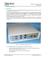
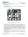
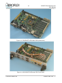
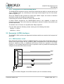
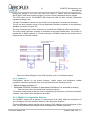
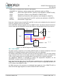
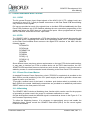
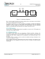
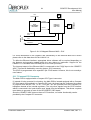
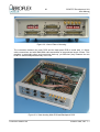
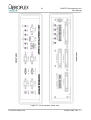
SPWRTC
Development Unit
User Manual
AEROFLEX GAISLER AB
Rev. 1.1, 2008-10-28
2
SPWRTC Development Unit
User Manual
Information furnished by Aeroflex Gaisler AB is believed to be accurate and reliable.
However, no responsibility is assumed by Aeroflex Gaisler AB for its use, nor for any infringements
of patents or other rights of third parties which may result from its use.
No license is granted by implication or otherwise under any patent or patent rights of Aeroflex
Gaisler AB.
Aeroflex Gaisler AB
tel +46 31 7758650
Kungsgatan 12
fax +46 31 421407
411 19 Göteborg
[email protected]
Sweden
www.aeroflex.com/gaisler
Copyright © 2008 Aeroflex Gaisler
All information is provided as is. There is no warranty that it is correct or suitable for any purpose,
neither implicit nor explicit.
© Aeroflex Gaisler AB
October 2008, Rev. 1.1
3
SPWRTC Development Unit
User Manual
TABLE OF CONTENTS
1
INTRODUCTION...........................................................................................................6
1.1
1.2
1.3
1.4
2
Overview......................................................................................................................6
References...................................................................................................................8
Handling.......................................................................................................................8
Abbreviations...............................................................................................................8
ELECTRICAL DESIGN.................................................................................................9
2.1
2.2
2.3
2.3.1
2.3.2
2.3.3
2.4
2.4.1
2.4.2
2.5
2.5.1
2.5.2
2.5.3
2.6
2.7
2.8
2.8.1
2.8.2
2.9
2.9.1
2.9.2
2.9.3
2.9.4
2.9.5
2.9.6
2.10
2.11
2.11.1
2.11.2
2.11.3
2.11.4
2.11.5
2.11.6
2.11.7
Block Diagram..............................................................................................................9
SPWRTC ASIC..........................................................................................................11
Memory......................................................................................................................11
SRAM.........................................................................................................................12
FLASH.......................................................................................................................12
EEPROM....................................................................................................................12
CAN Interface............................................................................................................12
Configuration of Bus Termination...............................................................................13
Configuration of Enable/Standby Mode......................................................................14
Spacewire (LVDS) Interfaces.....................................................................................14
SPW interface circuit..................................................................................................14
SPWCLK....................................................................................................................15
SPWCLK Configuration Switches..............................................................................15
Serial Interfaces and PIO...........................................................................................16
Debug Support Unit (DSU) Serial Interface................................................................16
Analog Interfaces ......................................................................................................17
ADC Inputs.................................................................................................................18
DAC Output................................................................................................................19
Oscillators and Clock Inputs.......................................................................................20
System Clock.............................................................................................................20
SPW_CLK..................................................................................................................20
TIMER_CLK...............................................................................................................20
Timer Triggers............................................................................................................21
UART_EXTCLK.........................................................................................................21
Ethernet Clock............................................................................................................21
Power Supply and Voltage Regulation......................................................................21
Other Interfaces and Circuits.....................................................................................22
GPIO..........................................................................................................................22
FIFO...........................................................................................................................22
Reset Circuit and Button............................................................................................22
Watchdog...................................................................................................................22
JTAG interface...........................................................................................................23
Ethernet Interface......................................................................................................23
Compact PCI Connector............................................................................................24
3
MECHANICAL DESIGN..............................................................................................25
4
SETTING UP AND USING THE UNIT........................................................................27
5
INTERFACES AND CONFIGURATION.....................................................................31
5.1
5.2
List of Front/Back Panel Connectors..........................................................................31
List of Connectors and Jumpers on Main PCB...........................................................41
© Aeroflex Gaisler AB
October 2008, Rev. 1.1
4
SPWRTC Development Unit
User Manual
LIST OF TABLES
Table 4-1: Default Status of Jumpers/Switches..............................................................................27
Table 5-1: List of Front/Back Panel Connectors.............................................................................31
Table 5-2: List and definition of Front/Back Panel Switches...........................................................31
Table 5-3: List and definition of Front Panel LED's........................................................................32
Table 5-4: J1 DSU - Debug Support Unit connections ..................................................................34
Table 5-5: J2 RJ45-ETHERNET Connector...................................................................................34
Table 5-6: J3 SPW-0 interface connections .................................................................................34
Table 5-7: J4 SPW-1 interface connections .................................................................................35
Table 5-8: J5 CANBUS-0 interface connections............................................................................35
Table 5-9: J6 CANBUS-1 interface connections............................................................................35
Table 5-10: J7 UART-1 - Serial Interface (RS232) connections ...................................................36
Table 5-11: J8 UART-2 - Serial Interface (RS232) connections ...................................................36
Table 5-12: J9 POWER – External Power Connector....................................................................36
Table 5-13: J10 SPW External Clock Input....................................................................................36
Table 5-14: J11 UART External Clock Input...................................................................................36
Table 5-15: J12 General Purpose External Clock signal................................................................37
Table 5-16: J13 Timer Trigger 1 Input............................................................................................37
Table 5-17: J14 Timer Trigger 2 Input............................................................................................37
Table 5-18: J15 Analog to Digital Conversion Trigger....................................................................37
Table 5-19: J16 ADC_IN0 Input.....................................................................................................37
Table 5-20: J17 ADC_IN1 Input.....................................................................................................37
Table 5-21: J18 ADC_IN2 Input.....................................................................................................37
Table 5-22: J19 ADC_IN3 Input....................................................................................................38
Table 5-23: J20 DAC output..........................................................................................................38
Table 5-24: P1 FIFO Header Pin out..............................................................................................38
Table 5-25: P2 GPIO[11..0] Header Pin out...................................................................................38
Table 5-26: P3 GPIO[23..12] Header Pin out.................................................................................39
Table 5-27: P4 PIO Header Pin out................................................................................................39
Table 5-28: DIP Switch S1 'SPWCLKCNFG' definition..................................................................40
Table 5-29: DIP Switch S2 'CONFIG' definition..............................................................................40
Table 5-30: DIP Switch S3 'PIO[7..0]' definition.............................................................................40
Table 5-31: DIP Switch S4 'PIO[15..8]' definition............................................................................40
Table 5-32: List of PCB Connectors...............................................................................................41
Table 5-33: Expansion connector J9 Pin-out..................................................................................42
Table 5-34: Expansion connector J11 Pin-out................................................................................43
Table 5-35: List and definition of PCB Jumpers.............................................................................44
Table 5-36: ADC_SIGS Header, JP5 pin-out.................................................................................45
Table 5-37: FIFO_SIGS Header, JP6 pin-out.................................................................................45
Table 5-38: GPIO_SIGS Header, JP7 pin-out................................................................................45
LIST OF FIGURES
Figure 1-1: SPWRTC Development Unit..........................................................................................6
Figure 2-1: Block Diagram of GR-SPWRTC-DEV board..................................................................9
Figure 2-2: GR-SPWRTC-DEV Main PCB (stand-alone)...............................................................10
Figure 2-3: GR-SPWRTC-DEV with CPCI Front Panel..................................................................10
Figure 2-4: SPWRTC ASIC............................................................................................................11
Figure 2-5: On-Board Memory Configuration.................................................................................11
Figure 2-6: Block Diagram of the CAN interface............................................................................13
Figure 2-7: Transceiver and Termination Configuration (one of 2 interfaces shown).....................13
Figure 2-8: Block Diagram of the SPW interface (one of 2 interfaces shown)................................14
© Aeroflex Gaisler AB
October 2008, Rev. 1.1
5
SPWRTC Development Unit
User Manual
Figure 2-9: Block Diagram of the SPW interface (one of 2 interfaces shown)................................15
Figure 2-10: PIO and UART interface............................................................................................16
Figure 2-11: Debug Support Unit connections................................................................................17
Figure 2-12: Block Diagram of the Analog Control interface..........................................................18
Figure 2-13: ADC Circuitry.............................................................................................................19
Figure 2-14: DAC Circuit................................................................................................................19
Figure 2-15: Clock Distribution Scheme.........................................................................................20
Figure 2-16: Power Supply and Voltage Regulation.......................................................................21
Figure 2-17: Watchdog configuration.............................................................................................23
Figure 2-18: I/O Mapped Ethernet MAC + PHY.............................................................................24
Figure 3-1: View of Front of Housing..............................................................................................25
Figure 3-2: View of Rear of Housing..............................................................................................26
Figure 3-3: View showing Main PCB and Backpanel PCB.............................................................26
Figure 4-1: GRMON Output Screenshot #1...................................................................................29
Figure 4-2: GRMON Output Screenshot #2...................................................................................30
Figure 5-1: Front and Back Panel View..........................................................................................33
Figure 5-2: Main PCB Top View.....................................................................................................46
REVISION HISTORY
Revision
Date
Page
0.1 DRAFT
2007-05-13 All
New document/draft
0.1 DRAFT2
2007-10-20 §1.1
Updated Figure 1-1 and indicated DSU link is optional RS232 or USB-toRS232 Converter; SMA connectors have been moved to front panel.
§2.7
Added new USB-to-RS232 interface connection
§3
Updated figures
§5
Added USB connector to list and tables. Updated figure 5-1.
All
Update of pictures and figures after hardware completion. Completed §4
1.0
2008-0410
1.1
2008-10-28 All
© Aeroflex Gaisler AB
Description
Formatting changed.
October 2008, Rev. 1.1
6
1
SPWRTC Development Unit
User Manual
INTRODUCTION
1.1 Overview
This document describes the GR-SPWRTC-DEV Development Unit which forms one part of
the SPWRTC Development Suite.
The purpose of this equipment is to provide developers with a convenient hardware platform
for the evaluation and development of software for the SpaceWire Remote Terminal
Controller (SPWRTC) ASIC device. The SPWRTC is a Leon2 based custom ASIC
developed in the scope of the “TopNet SpaceWire Controller / Remote User Interface”
activity initiated by the European Space Agency.
The GR-SPWRTC-DEV Unit comprises a custom designed PCB enclosed in a mechanical
housing. All the principle interfaces and functions are accessible on front and back panel
connectors.
Figure 1-1: SPWRTC Development Unit
The GR-SPWRTC-DEV Unit comprises the following main elements:
•
Main PCB incorporating SPWRTC ASIC, memory, interface and auxiliary circuits,
•
Back panel PCB with interface connections
•
Mechanical Housing, with custom front and rear panels
•
Internal cabling
© Aeroflex Gaisler AB
October 2008, Rev. 1.1
7
SPWRTC Development Unit
User Manual
The interface connectors on the Front Panel of the unit provide:
•
•
•
•
•
•
•
•
Serial DSU UART (RS232 or USB connector)
Ethernet
Two Spacewire interfaces
Two CAN bus interfaces
Two Serial UART interfaces (RS232)
Push Buttons for RESET and BREAK
Coaxial (SMA) type connectors for Analog Input/Output
LED indicators
To enable convenient connection to the interfaces, the connector types and pin-outs are
compatible with the standard connector types for these types of interfaces.
The interface connectors on the Back Panel of the unit provide:
•
•
•
•
•
Interface connectors for General Purpose I/O (GPIO - 24 signals)
Interface connectors for General Purpose I/O (PIO - 16 signals)
Interface connectors for FIFO data interface
Coaxial (SMA) type connectors for Clock inputs and Triggers
DIP switches for system configuration
The main PCB contains the following main items as detailed in section 2 of this document:
•
•
•
•
•
SPWRTC ASIC
Memory
• SRAM (2 banks x 2Mword x 40 Bits wide including EDAC)
• Flash PROM (2 banks x 64Mbit organised x8 bit wide)
• EEPROM (1 bank x 1Mbit, organised x8 bit wide)
• additional memory via memory expansion connector
•
Interfaces
• two CAN interfaces
• two Spacewire LVDS electrical interfaces
• two serial UART (RS232) interfaces
• 10/100MBit Ethernet controller and PHY
• DSU (Serial RS232) interface
•
On-board ADC and DAC circuits
• 4 channel analog inputs with 12 bit ADC (AD1674 with ADG509)
• 1 channel analog output with 12 bit DAC (AD667)
•
Timer and Trigger Inputs/Outputs
PIO (16 signals) and GPIO (24 signals) input/output connections
FIFO interface connections for high speed interface via external FIFO circuit
Power, Reset , Clock and Auxiliary circuits
© Aeroflex Gaisler AB
October 2008, Rev. 1.1
8
SPWRTC Development Unit
User Manual
1.2 References
RD-1
GR-SPWRTC-DEV_schematic.pdf, Schematic
RD-2
GR-SPWRTC-DEV_assy_drawing.pdf, Assembly Drawing
RD-3
P-ASIC-NOT-00256-SE, SpaceWire-RTC (SpwRtc) Datasheet
1.3 Handling
ATTENTION : OBSERVE PRECAUTIONS FOR
HANDLING ELECTROSTATIC SENSITIVE DEVICES
This unit contains sensitive electronic components which can be damaged by Electrostatic
Discharges (ESD). When handling or installing the unit observe appropriate precautions and
ESD safe practices.
When not in use, store the unit in an electrostatic protective container or bag.
When configuring the jumpers on the board, or connecting/disconnecting cables, ensure that
the unit is in an unpowered state.
1.4 Abbreviations
ADC
DAC
DIP
ESD
FIFO
FPGA
FP
FT
GPIO
I/O
IP
LVDS
MUX
PCB
SPW
Analog to Digital Converter
Digital to Analog Converter
Dual In-Line Plastic
Electro-Static Discharge
First-In First-Out
Field Programmable Gate Array
Front Panel
Fault-Tolerant
General Purpose Input / Output
Input/Output
Intellectual Property
Low Voltage Digital Signalling
Multiplexer
Printed Circuit Board
Spacewire
© Aeroflex Gaisler AB
October 2008, Rev. 1.1
9
2
SPWRTC Development Unit
User Manual
ELECTRICAL DESIGN
2.1 Block Diagram
ANALOG
CLOCK &
TRIGGERS
INTERNAL
CABLING
POWER
FIFO
GPIO
PIO
FIFO I/F
GPIO I/F
PIO I/F
BACKPANEL
PCB
The GR-SPWRTC-DEV unit provides the electrical functions and interfaces as represented
in the block diagram, Figure 2-1.
MAIN
PCB
DIP SWITCHES
ADC/DAC
CIRCUITS
SPWRTC
ASIC
POWER
&
AUX
CANBUS
UART/
RS232
SPW
2 x CAN
2 x UART
2 x SPW
FLASH
EEPROM
SRAM
MEMORY
EXPANSION
ADC/DAC
EXPANSION
ETHERNETPHY
DSU/
RS232
10/100 Mb
ETHERNET
SERIAL DSU
Figure 2-1: Block Diagram of GR-SPWRTC-DEV board
The Main PCB is of standard Double Eurocard format (233.35 x 160mm) and, in principle,
could be used 'stand-alone' on the bench-top, without a housing. The board is also is also
compatible with mounting in a 6U Compact PCI rack if a suitable front panel is fitted.
However, for this development, in order to provide a convenient development system, this
Main PCB will be mounted in a bench-top housing. The connectors on the front edge of the
Main PCB can be directly mounted to the front panel of the housing. However, a separate
Back Panel PCB is required in order to accommodate the connections to the remaining
interfaces and to provide mounting for the DIP switches. The two PCB's are connected by
short lengths of ribbon cable.
Figure 2-2 shows the Main PCB and Figure 2-3 shows the Main PBC with 6U x 2 slot CPCI
front panel mounted.
Additionally, cabling is required to connect the coaxial connectors on the Main PCB to the
panel mounted connectors on the back panel and from the power connector on the back
panel to the Main PCB.
© Aeroflex Gaisler AB
October 2008, Rev. 1.1
10
SPWRTC Development Unit
User Manual
Figure 2-2: GR-SPWRTC-DEV Main PCB (stand-alone)
Figure 2-3: GR-SPWRTC-DEV with CPCI Front Panel
© Aeroflex Gaisler AB
October 2008, Rev. 1.1
11
SPWRTC Development Unit
User Manual
2.2 SPWRTC ASIC
The Main-PCB incorporates a Column Grid Array socket (type: Adapt-Plus CL349SA1912F)
to accommodate the SpaceWire-RTC ASIC in its MCGA349 Column Grid Array package.
Details of the interfaces, operation and programming of the SPWRTC ASIC is given in the
SPWRTC Datasheet, RD-3.
Figure 2-4: SPWRTC ASIC
2.3 Memory
The memory configuration installed on the Main PCB is shown in the figure below comprising
of:
•
160Mbit of SRAM memory, organised as 2 banks x 2Mword x 40 bits wide
•
128Mbit of Flash PROM, organised as 2 banks x 8 MByte x 8 bits wide)
•
1Mbit of EEPROM organised as 1 bank x 128kByte x 8 bits wide)
Additionally, in order to allow users to install alternative memory configurations or devices, all
the signals of the memory interface are connected to memory expansion connectors. The
expansion connectors allow mezzanine boards to be added similar to those developed for
the existing GR-CPCI development boards.
ADDR
8
EEPROM
SPWRTC
ASIC
SRAM
SRAM
SRAM
SRAM
SRAM
BANK0
SRAM
SRAM
SRAM
SRAM
SRAM
ROMSN0
CONTROL
ROMSN1
FLASH
(32+8)
BANK1
RAMSN1
ROMSN0
FLASH
8
MEMORY EXPANSION CONNECTOR
DATA
Figure 2-5: On-Board Memory Configuration
© Aeroflex Gaisler AB
October 2008, Rev. 1.1
12
SPWRTC Development Unit
User Manual
2.3.1 SRAM
The GR-SPWRTC-DEV board two SRAM memory banks has mounted as standard, each
made up of five CY7C1069AV33. These devices are 16Mbit (2Mbyte x 8 bit devices with 10
or 12 ns access times.
The five devices provide (32 + 8) bit wide SRAM memory paths allowing EDAC operation.
These memory banks are mapped as RAMBANK0 and RAMBANK1.
In case the user wishes to disable the on board memory, this can be done by removing the
jumpers JP9 on the Main-PCB.
2.3.2 FLASH
The GR-SPWRTC-DEV board has mounted as standard two FLASH memory banks, each
made up of one Intel JS28F640J3 FLASH device. These devices are 64Mbit (8Mbyte x 8 bit
devices), typically with 115ns access times. The data bus width to the Flash memory is 8 bits
wide. Each of the Flash devices is addressed by one of the two ROMBANK select control
signals.
Note that, in Leon2 designs, the PROM width and PROM EDAC conditions are set by the
state of the PIO[2..0] pins at power up of the Processor. Therefore the PIO[2..0] DIP
switches on the Back Panel must be appropriately set for the correct operation of the PROM
memory at start up of the processor. For information on the PIO[2..0] settings refer to the
Memory Configuration documentation in the Leon2 User Manual, or RD-3.
2.3.3 EEPROM
The GR-SPWRTC-DEV board additionally has a DIP32 socket suitable for mounting an
EEPROM device. The data bus width to the EEPROM device is 8 bits wide.
This socket is suitable for mounting an EEPROM device of the type AT28LV010, or
compatible, in DIP32 package. The AT28LV010 is an ATMEL EEPROM, of 1Mbit capacity
organises as 128kByte x 8 bits.
Note though that the Leon2 memory controller design has only two ROMBANK select control
signals and it is not possible to simultaneously use the EEPROM memory together with both
the Flash ROM banks.
Jumpers are therefore provided to enable the user to select either the first FLASH device or
the EEPROM to operate as the ROMBANK0 device which appears at the initial memory
location of 0x00000000.
2.4 CAN Interface
The Main-PCB provides the electrical interfaces for two CAN bus interfaces, as represented
in the block diagram, Figure 2-6.
The CAN bus transceiver IC's on this board are SN65HVD230 devices from Texas
Instruments which operate from a single +3.3V power supply.
The connector interfaces are male DSUB-9 connectors adhering to the standard pin-out for
this type of interface (ref. Table 5-8 And Table 5-9).
Although there are two CANBUS interfaces, inside the SPWRTC ASIC there is only one
controller which is multiplexed between the two interfaces.
The ENABLE signals are used to drive LED's to provide an indication of the active CAN
interface. LED's are provided on the front panel if the unit.
© Aeroflex Gaisler AB
October 2008, Rev. 1.1
13
CAN
TRANSCEIVER
CAN_L
ENABLE
TXD
RXD
CAN_H
CAN
TRANSCEIVER
CAN_L
CAN
interface 2
CONTROLLER LOGIC IN ASIC
RXD
CAN_H
CAN
interface 1
TXD
SPWRTC Development Unit
User Manual
ENABLE
Figure 2-6: Block Diagram of the CAN interface
2.4.1 Configuration of Bus Termination
The CAN interfaces on the board can be configured for either end node or stub-node
operation by means of the jumpers JP3 and JP4 for interface 1 and 2 respectively, as shown
in Figure 2-7.
For normal end-node termination with a nominal 120 Ohm insert jumpers in position 1-3.
However, if a split termination is desired (if required for improved EMC performance), insert
the jumpers in positions 1-2 and 3-4.
For stub nodes, if termination is not required, do not install any jumpers.
Figure 2-7: Transceiver and Termination Configuration (one of 2 interfaces shown)
© Aeroflex Gaisler AB
October 2008, Rev. 1.1
14
SPWRTC Development Unit
User Manual
2.4.2 Configuration of Enable/Standby Mode
The SN65HVD230 transceiver device used on the board has the facility to set the device into
either STANDBY mode, by connecting an active high external signal to pin 8 of the device
(refer to Figure 2-7).
Since the SPWRTC ASIC provides an active high 'enable' output, an inverter is therefore
required to control the standby pin appropriately.
Conveniently this inverter can also be used to drive an LED.
A further feature provided by the SN65HVD230 device is the capability to adjust the
transceiver slew rate. This can be done by modifying the values of resistors connected to pin
8 of the transceivers.
The default value of 0 ohms is compatible with 1Mbps operation.
From the data sheet the following resistor values give the following slew rates:
10kOhm => 15V/us
100kOhm => 2V/us
2.5 Spacewire (LVDS) Interfaces
The SPWRTC ASIC provides two Spacewire interfaces which are routed to the front panel of
the board.
2.5.1 SPW interface circuit
Each Spacewire interface consists of 4 differential pairs (2 input pairs and 2 output pairs), as
shown in the figure below. As the SPWRTC ASIC incorporates the LVDS driver/receiver
structures inside the ASIC, no additional LVDS driver circuits are required on the PCB.
However a 1.25V Voltage Reference circuit is required in order to provide the necessary bias
voltages for the driver and receiver circuits.
P
DOUT+
DOUT-
N
ASIC
LOGIC
P
SOUT+
SOUT-
N
P
DIN+
DIN-
N
P
SIN+
SIN-
N
Vref
MEZZANINE
CONNECTOR
Figure 2-8: Block Diagram of the SPW interface (one of 2 interfaces shown)
© Aeroflex Gaisler AB
October 2008, Rev. 1.1
15
SPWRTC Development Unit
User Manual
During the design of the PCB care has been taken to ensure that has SIN/DIN and
SOUT/DOUT pairs have matched lengths, to ensure equal propagation time for signals
The PCB traces on the GR-SPWRTC-DEV board are laid out with 100-Ohm differential
impedance design rules.
100 Ohm Termination resistors for the LVDS receiver signals are mounted on the board.
The pin out and connector types for these Spacewire interfaces conforms to the Spacewire
standard, as shown in Figure 2-9.
The inner shield pin (pin3 of the connector) is connected to DGND via a Zero-ohm resistor.
The outer shield (connector chassis) is connected to the board DGND with a 10k resistor in
parallel with a 100pF capacitor. If a 'hard' connection to DGND is desired, the resistor can be
replaced with a Zero-ohm resistor.
Figure 2-9: Block Diagram of the SPW interface (one of 2 interfaces shown)
2.5.2 SPWCLK
Configuration options on the board (jumpers, crystal socket and backpanel coaxial
connector) allow this Spacewire clock to be provided from the following sources:
•
•
Main processor oscillator X1
Dedicated SPWCLK oscillator (if appropriate Oscillator X3 is mounted in socket)
•
External clock input (from back panel coaxial connector)
The default configuration is that the clock is supplied by the frequency of the main processor
oscillator, with jumper JP23 installed on the board.
2.5.3 SPWCLK Configuration Switches
The SPWRTC design has a number of control inputs to the ASIC which are required to be
set to configure the clock and PLL features of the Spacewire interface.
These configuration signals can be set by means of DIP Switches on the back panel of the
Unit. The DIP switches on the Back Panel are assigned the following functions:
© Aeroflex Gaisler AB
October 2008, Rev. 1.1
16
SPWCLKCFG0
SPWCLKCFG1
SPWCLKCFG2
SPWCLKCFG3
SPWCLKCFG4
SPWCLKCFG5
SPWCLKCFG6
SPWCLKCFG7
SPWCLKCFG8
=>
=>
=>
=>
=>
=>
=>
=>
=>
SPWRTC Development Unit
User Manual
SPWCLK10Mbit0
SPWCLK10Mbit1
SPWCLK10Mbit2
SPWCLKMULT0
SPWCLKMULT1
SPWCLKMUXSEL
SPWCLKPLLCFG0
SPWCLKPLLCFG1
SPWCLKPLLCFG2
For more information on the meaning and operation of these signals, refer to RD-3.
2.6 Serial Interfaces and PIO
The standard Leon2 design on which the SPWRTC is based, provides a 16 bit Parallel Input/
Output port (PIO). These 16 pins are routed from the ASIC to the Backplane PCB where
external connections can be made to the PIO pins for control or monitoring of the state of the
pins.Additionally on the back panel PCB, DIP switches are provided to allow a easy setting
of the PIO configuration if required.
In the Leon2 design the to 8 bits of the PIO port have a dual function and can be used to
provide two serial UART interfaces. The GR-SPWRTC-DEV design provides RS232
driver/receiver chips for these signals and routes these to front panel connectors. To enable
the use of these pins for the UART functions, jumpers must be installed, and the
corresponding DIP switches must be opened, as schematically represented in Figure 2-10.
The front panel connector types for the UART interfaces are Female D-Sub 9 pin types with
a standard pin-out for serial links.
PULL-UP
(x16)
SPWRTC
ASIC
16
PIO[15..0]
PIO[15..0]
DIP-SW
(x16)
2 x RS232
INTERFACE
RS232
DRIVER/
RECEIVERS
8
PIO[15..8]
MAIN
PCB
BACKPANEL
PCB
Figure 2-10: PIO and UART interface
2.7 Debug Support Unit (DSU) Serial Interface
The GR-SPWRTC-DEV unit provides a interface for Debug and control of the processor by
means of a host terminal via the DSU serial link to the SPWRTC ASIC, as represented in
Figure 2-11.
© Aeroflex Gaisler AB
October 2008, Rev. 1.1
17
SPWRTC Development Unit
User Manual
USB
USB to SERIAL
CONVERTER
RS232 SERIAL
HOST
TERMINAL/COMPUTER
RS232
DRIVER/
RECEIVER
DSURX→
DSUBRE→
DSUACT←
DSU I/F
DSUTX←
MUX
SPWRTC
ASIC
DSUEN→
Figure 2-11: Debug Support Unit connections
The unit provides two possibilities for connecting to the Serial DSU interfaces:
1. SUB-D Female 9 pin serial connector with RS232 transceiver
2. USB MiniAB connector with USB to Serial interface chip
Spare logic in the CPLD (which is already required for the address decoding of the
Ethernetinterface- see section 2.11.6) is used to implement a simple multiplexer to connect
the two sets of RX/TX signals to the DSURX and DSUTX signals of the SPWRTC ASIC
chip.
The control signal for the multiplexer is derived from the +5V pin of the USB connector
sothat when a powered USB cable is plugged into the unit the USB cable is selected as the
active DSU interface.
The baud rate of the serial link is determined by the host computer, and the DSU interface in
the SPWRTC ASIC auto-detects and adjusts its baud rate to suit.
The DSUENable signal input to the processor is connected to a DIP switch on the back
panel of the unit (ref. Table 5-29). In normal use the DSU feature will always be enabled to
allow processor control and program debugging via the DSU link.
Two LED's are provided on the Main PCB to indicate the conditions of the DSUACT and
ERRORN signals from the SPWRTC processor. Additionally connections are provided to two
LED's indicators on the front panel of the Unit.
A miniature push button switch is provided on the Main PCB for the DSUBREAK control, and
connections are provided to an additional push-button switch on the front panel of the unit.
2.8 Analog Interfaces
The GR-SPWRTC-DEV board includes and ADC and DAC circuits on board, intended to be
used to demonstrate the operation of ADC/DAC controller IP-core which is implemented in
the logic of the SPWRTC ASIC.
The signals of this IP-core interface are provided on connector JP5 to enable probing and
monitoring of the signals.
This IP-core interface is intended to be multi-purpose, and suitable for different types of
ADC/DAC components, and comprises the following signals:
© Aeroflex Gaisler AB
October 2008, Rev. 1.1
18
SPWRTC Development Unit
User Manual
ADDATA[15..0] Bussed ADC and DAC data signals
ADADDR[7..0] Multiplexer address signals (Also individually usable as GPIO)
ADWR
Write control signal for DAC (polarity is user-definable in SPWRTC ASIC)
ADCS
Chip Select (polarity is user-definable in SPWRTC ASIC)
ADRC
Read/Convert control for ADC (polarity is user-definable in SPWRTC)
ADRDY
Conversion ready signal from ADC (polarity user-definable in SPWRTC)
ADTRIG
External ADC Trigger input
Note that, if desired, the on-board ADC and DAC circuits can be disabled, by the removal of
as set of 4 jumpers (JP10) on the board.
All the ADC/DAC interface signals from the SPWRTC ASIC. This allows simple interface for
users to add their own Mezzanine boards with different Analog/Digital features as required.
ADCS
ADRC
ADRDY
ADC
MUX
ADC_IN
FPGA
LOGIC
ADDATA[15..0]
SPWRTC
ASIC
ADTRIG
TRIGGER
ADADDR[7..0]
ADWR
DAC_OUT
DAC
Figure 2-12: Block Diagram of the Analog Control interface
2.8.1 ADC Inputs
The ADC circuitry comprises a 12 bit ADC (AD1674) with a 4 channel multiplexer front-end
(ADG509). For detailed operation of the ADC please refer to its datasheet.
The default configuration of the ADC is set-up to measure a bipolar -5V to +5V input voltage
range. However, the circuit on the board can also be configured to provide a uni-polar 0 to
+10V or input voltage range, by reconfiguration of a number of the resistors on-board.
The Multiplexer address is controlled by setting the appropriate bit-pattern on the
ADADDR[5..4] signal outputs of the SPWRTC ASIC.
Note that, since the logic part of the ADC device operates from a +5V digital supply, the
output data must be buffered with a level shifter circuit to ensure compatibility with the 3.3V
LVTTL inputs of the SPWRTC ASIC.
An SMA connector (J19) connects to a dedicated input signal pin of the SPWRTC ASIC to
allow an external trigger signal to be used to initiate an ADC conversion.
© Aeroflex Gaisler AB
October 2008, Rev. 1.1
19
SPWRTC Development Unit
User Manual
Figure 2-13: ADC Circuitry
2.8.2 DAC Output
The DAC circuitry comprises a single channel 12 bit DAC (AD667) .
The default configuration of the DAC is set-up to provide a bipolar -5V to +5V output voltage
range. However, the circuit on the board can also be configured to provide a uni-polar 0 to
+10V or 0 to +5V output voltage range, by reconfiguration of a number of the resistors onboard. Additionally Offset and Gain of the DAC circuit can be adjusted by means of the onboard potentiometers.
For detailed operation of the DAC please refer the schematic and the datasheet of the DAC
device.
Figure 2-14: DAC Circuit
© Aeroflex Gaisler AB
October 2008, Rev. 1.1
20
SPWRTC Development Unit
User Manual
2.9 Oscillators and Clock Inputs
The oscillator and clock scheme for the SPWRTC ASIC is shown in Figure 2-15.
MEMORY EXPANSION
CONNECTOR
ZERO
DELAY
BUFFER
TBD MHz
SYS CLK
DIL8 SOCKET
SPWRTC
ASIC
COAX CONNECTOR
TBD MHz
SPW CLK
DIL8 SOCKET
COAX CONNECTOR
TIMER CLK
TBD MHz
DIL8 SOCKET
CPLD
Ethernet
Controller
& PHY
25 MHz
SMD
COAX CONNECTOR
TIMER_TRIG1
COAX CONNECTOR
TIMER_TRIG2
Figure 2-15: Clock Distribution Scheme
2.9.1 System Clock
The main oscillator for the SPWRTC ASIC is a 30 MHz Crystal oscillator. This oscillator will
be a 4 pin DIL8 style oscillator, installed in a socket on the board. A zero-delay buffer circuit
(CY2305) is used to distribute the SYSCLK.
2.9.2 SPW_CLK
The SPWCLK can be derived from either the SYSCLK, a separate socketed on-board crystal
oscillator, or can be injected on a coaxial connector on the rear panel of the unit.
2.9.3 TIMER_CLK
One SMA connector (J15) is defined to allow an external clock frequency to be injected for
for generating the clock of the General Purpose Timers in the Leon system. Alternatively a
dedicated oscillator can be installed in a DIL8 socket on the board.
© Aeroflex Gaisler AB
October 2008, Rev. 1.1
21
SPWRTC Development Unit
User Manual
2.9.4 Timer Triggers
Two coaxial connectors (J20 and J21) are defined for the functions of Timer Trigger inputs to
allow an external equipment to generate these trigger inputs.
2.9.5 UART_EXTCLK
A further coaxial connector on the rear panel (J23) is defined to allow an external clock
frequency to be injected for generating the clock of the UART (serial) interface
communication. This signal is connected to the PIO(3) input of the SPWRTC ASIC (see
RD-3).
2.9.6 Ethernet Clock
A dedicated 25MHz SMD oscillator is provided for the Ethernet Controller and PHY circuit
(see section 2.11.6).
2.10 Power Supply and Voltage Regulation
The board operates from a single +5V DC power supply input. On board regulators generate
the following voltages:
•
+3.3V for the SPWRTC I/O voltage, memory chip and other peripherals
•
+1.8V for SPWRTC Vcore voltage
•
+12V for analog circuits (ADC and DAC)
•
-12V for analog circuits (ADC and DAC)
+5V DC
power
input
+3.3V_CPCI
DC/DC
5V to 3.3V
+3.3V
VI/O for SPWRTC
& GENERAL I/O
DC/DC
5V to 1.8V
+1.8V
Vcore for
SPWRTC
DC/DC
5V to 12V
+12V
Analog &
Mezz conn.
CPCI
connector
+5V_CPCI
+12V_CPCI
DC/DC
5V to -12V
-12V
Analog &
Mezz conn.
-12V_CPCI
Figure 2-16: Power Supply and Voltage Regulation
All voltages +5V, +3.3V, ±12V are provided via the memory expansion connector interface
making feasible that user defined mezzanine boards can use these voltages.
If the Main PCB is installed in a Compact PCI rack, the board can be configured by means of
jumpers such that the +5V, +3.3V, +12V and -12V are provided from the Compact PCI
backplane instead of the internal regulators.
© Aeroflex Gaisler AB
October 2008, Rev. 1.1
22
SPWRTC Development Unit
User Manual
2.11 Other Interfaces and Circuits
2.11.1 GPIO
The 24 general Purpose Input Output signals of the ASIC(3.3V LVTTL voltage levels) are
connected to a set of 0.1” pitch pin header connectors on the Rear Panel PCB thus allowing
easy access to these signals.
Pull ups are provided on each of the signals lines on the Main PCB and additionally the Rear
Panel PCB provides a set of DIP Switches allowing the user convenient programming of the
signal state when the GPIO lines are configured as inputs. When programmed as outputs
the DIP switches should be left in the 'open' state.
2.11.2 FIFO
The SPWRTC ASIC is equipped with a FIFO data interface for high-speed data transfer with
an external device, supporting both 8 and 16 bit operational mode. A 0.1” connector header
on the Rear Panel enables direct access to the digital FIFO interface of the ASIC with the
following signals:
FIFOHALFN
FIFOFULLN
FIFOEMPTYN
FIFOWRN
FIFORDN
FIFOP[1..0]
FIFOD[15..0]
RESETN
Since different users may have various requirements on the type FIFO device and interface,
or may want to interface an FPGA or similar device via the FIFO data interface, the GRSPWRTC-DEV board itself does not include any such circuits. However, such circuits can be
added by means of a small mezzanine board connecting to the Rear Panel FIFO connector.
2.11.3 Reset Circuit and Button
A standard Processor Power Supervisory circuit (TPS3705 or equivalent) is provided on the
Main PCB to provide monitoring of the 3.3V power supply rail and to generate a clean reset
signal at power up of the Unit.
To provide a manual reset of the board, a miniature push button switch is provided on the
Main PCB for the control. Additionally connections are provided to an additional push-button
RESET switch on the front panel of the unit.
2.11.4 Watchdog
The SPWRTC ASIC includes a Watchdog timer function which can be used for the purpose
of generating a system reset in the event of a software malfunction or crash.
On this development board the WDOGN signal is connected as shown in the Figure 2-17 to
the Processor Supervisory circuit.
To utilise the Watchdog feature, it is necessary to appropriately set-up and enable the
Watchdog timer. Please consult the SPWRTC data sheet (RD-3) for the correct register
locations and details.
© Aeroflex Gaisler AB
October 2008, Rev. 1.1
23
FRONT
PANEL
LED
RESETN
SPWRTC
ASIC
SPWRTC Development Unit
User Manual
BOARD
MOUNTED
LED
WDOGN
RSTIN_N
SWITCH
S2-4
POWER-ON
RESET
CIRCUIT
Figure 2-17: Watchdog configuration
Also, to allow the WDOGN signal to generate a system reset it is necessary to set the Switch
S2-4 in the CLOSED position (see Figure 2-17).
For software development it is often convenient or necessary to disable the Watchdog
triggering in order to be able to easily debug without interference from the Watchdog
operation. In this case, Switch S2-4 should be in the OPEN position. When the watchdog
triggers, the Watchdog LED's will illuminate, but a system reset will not occur.
2.11.5 JTAG interface
A 6 pin header on the Main PCB provides the possibility to connect to the JTAG signals and
JTAG chain of the SPWRTC ASIC.
2.11.6 Ethernet Interface
The SPWRTC ASIC device does not incorporate a Ethernet interface. However, this
functionality is implemented on the GR-SPWRTC-DEV board by adding an external Ethernet
controller and PHY device, mapped as an I/O peripheral in the memory/IO space of the
processor.
A separate CPLD is required in order to perform the address and logic decoding for the
control of the LAN91C111 device.
In the example configuration programmed into the CPLD at delivery, the registers of the
Ethernet MAC+PHY are mapped at the start of the Leon I/O space at memory address
0x20000000.
© Aeroflex Gaisler AB
October 2008, Rev. 1.1
24
SPWRTC Development Unit
User Manual
OSC
25MHz
JTAG
PROGRAMMING
MEMORY
BUS
CPLD
FOR ADDRESS
DECODING
RESET
LAN91C111
ETHERNET
MAC + PHY
RJ45
ETHERNET
ENABLE
MEM CTRL &
ADDR
DATA
JP2
INTERRUPT
(PIO[4])
Figure 2-18: I/O Mapped Ethernet MAC + PHY
For more information on the registers and functionality of the Ethernet MAC+PHY device
please refer to the data sheet for the LAN91C111.
To utilise the Ethernet interface, appropriate driver software will be required depending on
the features and operating system which the user wishes to implement. Support for the
LAN91C111 is included in the RTEMS port for the Leon processor.
The interrupt output of the Ethernet MAC is connected to the PIO[4] input to the SPWRTC
ASIC. This can be disabled by removing jumper JP2 if necessary.
The CPLD is programmed via a separate 6 pin JTAG header. However, this is not normally a
user feature.
2.11.7 Compact PCI Connector
The Main PCB is equipped with a Compact CPI Type-A connector.
If, instead of being mounted in a housing, the Main PCB is instead equipped with a Compact
PCI front panel and installed in a Compact PCI rack, the board can be configured by means
of jumpers such that the +5V, +3.3V, +12V and -12V are provided from the Compact PCI
backplane instead of the internal regulators. The only other signals form the CPCI interface
which is connected is the 'push button reset' signal form the backplane. This allows a system
reset button to generate a reset of the GR-SPWRTC-DEV board.
Since the SPWRTC ASIC does not have a PCI interface, no further functionality can be
provided by the Compact PCI connector.
© Aeroflex Gaisler AB
October 2008, Rev. 1.1
25
3
SPWRTC Development Unit
User Manual
MECHANICAL DESIGN
The housing provides a robust mechanical enclosure and convenient connector attachment
for convenient use in a laboratory or bench top environment.
The chosen housing type is: ELMA Type 33, case size 2 with depth 240mm. The overall
dimensions of the unit are 256.5 x 264 x 69 mm.
This housing is convenient in that it allows a PCB with 6U compatible (i.e. Double Euro Card
sized) width to be slotted into and supported by mounting rails in the housing itself.
The depth of the housing (240mm) is conveniently allows space for the backpanel PCB and
internal cabling.
The standard enclosure type has been selected and has an aluminium body and plastic
bezels and feet. This type of enclosure is also available in IP54 splash and dust resistant
and in EMC sealed versions.
Custom aluminium front panels are required, dimensioned with the appropriate cut-outs for
the connectors and indicators.
The connector types are 'standard' types allowing convenient attachment using standard
laboratory equipment.
Normally, no access would be required to the PCB's inside the housing, as connectors
provide connections to all the system interfaces, and rear-panel DIP switches provide
configuration options for the main features. However, access to the PCB's can easily be
gained by removing the rear bezel so that the rear panel can be loosened by means of 4
screws underneath the bezel. This then allows the lid to be removed without further
disassembly of the unit being performed.
Figure 3-1 shows a front view of the unit, showing the main system interface connectors.
Figure 3-2 shows a rear view of the unit, highlighting the configuration DIP switches, the
SMA type RF connectors for the analog and clock signals, and the FIFO/PIO and GPIO
interfaces. The connector types for the FIFO/PIO and GPIO interfaces are compatible with
IDC type ribbon cable connectors, and provide side latches to lock the mating connectors
and ensure contact.. These type of connectors (0.1” raster pins) are also simple to connect
to individual pins if simple monitoring of the states of outputs is required using lab equipment
(Oscilloscope or Logic Analyser). The unit is powered with a +5V DC power source which
connects to a connector on the back panel.
Figure 3-3 shows a view of the housing with the lid removed, to highlight the main and back
panel PCB's.
Figure 3-1: View of Front of Housing
© Aeroflex Gaisler AB
October 2008, Rev. 1.1
26
SPWRTC Development Unit
User Manual
Figure 3-2: View of Rear of Housing
The connection between the main PCB and the back-panel PCB is made with 1:1 ribbon
cable connections and with SMA-SMA cable assemblies of approximate length 150mm. This
provides a reasonably clean and convenient hook-up, yet sufficient 'play' between the two
PCB's to aid assembly/disassembly of the unit.
Figure 3-3: View showing Main PCB and Backpanel PCB
© Aeroflex Gaisler AB
October 2008, Rev. 1.1
27
4
SPWRTC Development Unit
User Manual
SETTING UP AND USING THE UNIT
The default status of the Jumpers on the boards is as shown in table Figure 4-1. For the
meaning of the various jumpers, refer to Table 5-35 and RD 1.
JP1
JP2
JP3
JP4
JP5
JP6
JP7
JP8
JP9
JP10
JP11
JP12
JP13
JP14
JP15
JP16
JP17
JP18
JP19
JP20
JP21
JP22
JP23
JP24
JP25
Stand-Alone Board
3-4
1-2
1-2
1-2
All open
All open
All open
1-2
All installed
All installed
1-2 and 3-4
Open
1-2
1-2 and 3-4
1-2
1-2
1-2
1-2
Open
1-2
All installed
1-2, 5-6, 7-8, 9-10
1-2
Open
1-2
Boxed Version
3-4
1-2
1-2
1-2
All open
All open
All open
1-2
All installed
All installed
1-2 and 3-4
CPCI-LED installed
1-2
1-2 and 3-4
1-2
1-2
1-2
1-2
Cable to FP Switch installed
1-2
All installed
1-2 -5-6, 7-8, 9-10
1-2
Cable to FP LED installed
1-2
Table 4-1: Default Status of Jumpers/Switches
To operate the unit, connect the +5V power supply to the Power Socket at the back of the
unit.
The front-panel POWER LED should be illuminated indicating that the +3.3V power is active.
Upon power on, the Processor will start executing instructions beginning at the memory
location 0x00000000, which is the start of the PROM. If the PROM is 'empty' or no valid
program is installed, the first executed instruction will be invalid, and the processor will halt
with an ERROR condition, with the ERROR LED illuminated.
Pressing the DSU-BREAK button should illuminate the DSUACT LED and halt the
processor.
To perform software download and debugging on the processor, a link from the Host
computer to the DSU interface of the board is necessary.
For PC's with a serial (SUBD-9) interface, the serial cable can be connected from the Host
© Aeroflex Gaisler AB
October 2008, Rev. 1.1
28
SPWRTC Development Unit
User Manual
PC to the J1 connector on the front Panel.
Alternatively, for PC's with only a USB interface, a connection to the DSU of the board can
be made using a USB cable (Type-A to Mini-AB connectors) from the Host PC to the USBDSU connector on the front panel.
Note, to use the USB-DSU interface you need to install the FTDI Virtual Com driver on the
Host PC. This driver allows the USB connection to the board to be used as a 'virtual' serial
port, operating at baud rates up to 460800 Baud.
These drivers can be downloaded from the FTDI web site, (www.ftdichip.com/FTDrivers.htm)
and drivers for both Linux and Windows are available. Information for the installation of
these drivers can be found on the FTDI web site
To perform program download and software debugging on the hardware it is necessary to
use the Gaisler Research GRMON debugging software, installed on a host PC (as
represented in Figure 2-11).
Note that it is necessary to use the 'PRO' version of GRMON, as the SPWRTC ASIC
incorporates FT features. It is not possible to use evaluation version of GRMON with this
ASIC. Please refer to the GRMON documentation for the installation of the software on the
host PC (Linux or Windows), and for the installation of the associated hardware dongle.
Starting GRMON, with the command:
grmon -i
will establish a link to the DSU, and will initialise the processor registers and timers.
The default serial interface used by GRMON is /dev/ttyS0 (linux) or com1 (Windows).
To use a different serial interface, specify the command
grmon -i -uart /dev/comXX
where XX is the number of the com port.
The resulting response generated on the Host Computer is shown in Figure 4-1.
Typing the command flash will reported the detected Flash Prom memory configuration and
info sys will provide more information on the processors registers and internal cores as
shown in Figure 4-2.
Program download and debugging can be performed in the usual manner. More information
on the usage, commands and debugging features of GRMON, is given in the GRMON Users
Manual and associated documentation.
.
© Aeroflex Gaisler AB
October 2008, Rev. 1.1
29
SPWRTC Development Unit
User Manual
Figure 4-1: GRMON Output Screenshot #1
© Aeroflex Gaisler AB
October 2008, Rev. 1.1
30
SPWRTC Development Unit
User Manual
Figure 4-2: GRMON Output Screenshot #2
© Aeroflex Gaisler AB
October 2008, Rev. 1.1
31
5
SPWRTC Development Unit
User Manual
INTERFACES AND CONFIGURATION
5.1 List of Front/Back Panel Connectors
Name
Function
Type
Description
J1
DSU
D9 FEMALE
Debug Support Unit serial connections
J2
ETHERNET
RJ45
10/100Mbit/s Ethernet Connector
J3
SPW-0
MDM9-S (female)
LVDS connections for Spacewire Interface-2
J4
SPW-1
MDM9-S (female)
LVDS connections for Spacewire Interface-1
J5
CANBUS-0
D9-P (male)
Connections for CANBUS-0 interface
J6
CANBUS-1
D9-P (male)
Connections for CANBUS-1 interface
J7
UART-1
D9-S (Female)
Connections for Serial UART-1 (RS232)
J8
UART-2
D9-S (Female)
Connections for Serial UART-2 (RS232)
J9
POWER-IN
2.1mm center +ve
+5V DC power input connector
P1
FIFO-IF
26 pin 0.1” Header
Pin connections for External FIFO interface
P2
GPIO[11..0]
26 pin 0.1” Header
Pin connections for GPIO signals 0 to 11
P3
GPIO[23..12]
26 pin 0.1” Header
Pin connections for GPIO signals 12 to 23
P4
PIO[15..0]
34 pin 0.1” Header
Pin connections for PIO signals 0 to 15
J10
SPW_CLK
SMA-JACK
Input for External SPW clock signal
J11
UART_EXTCLK
SMA-JACK
Input for External UART clock signal
J12
GP_EXTCLK
SMA-JACK
General Purpose Clock input
J13
TIMETRIG1
SMA-JACK
Timer 1 Trigger Output
J14
TIMETRIG2
SMA-JACK
Timer 2 Trigger Output
J15
ADC_TRIG
SMA-JACK
ADC Trigger Input
J16
ADC_IN0
SMA-JACK
Analog Mux input Channel 0
J17
ADC_IN1
SMA-JACK
Analog Mux input Channel 1
J18
ADC_IN2
SMA-JACK
Analog Mux input Channel 2
J19
ADC_IN3
SMA-JACK
Analog Mux input Channel 3
J20
DAC_OUT
SMA-JACK
Analog (DAC) Out
Table 5-1: List of Front/Back Panel Connectors
Name
Function
Description
S1
RESET
Push button RESET switch
S2
DSU_BREAK
Push button DSU_BREAK switch
S3
SPWCLKCNFG
8 pole DIP switch for SPW configuration
S4
CONFIG
4 pole DIP switch for general configuration
S5
PIO[7..0]
8 pole DIP switch for PIO configuration, bits 0 to 7
S6
PIO15..8]
8 pole DIP switch for PIO configuration, bits 8 to 15
Table 5-2: List and definition of Front/Back Panel Switches
© Aeroflex Gaisler AB
October 2008, Rev. 1.1
32
Name
Function
Description
D1
POWER (3.3V)
Power indicator
D2
ERRORN
Leon processor in 'ERROR' mode
D3
DSUACT
Leon Debug Support Unit 'Active'
D4
WDOG
Watchdog indicator.
D6
CAN-A
CAN interface A enabled
D7
CAN-B
CAN interface B enabled
D14
USB-RX
Indicates activity on USB RX data
D15
USB-TX
Indicates activity on USB TX data
SPWRTC Development Unit
User Manual
Table 5-3: List and definition of Front Panel LED's
© Aeroflex Gaisler AB
October 2008, Rev. 1.1
33
SPWRTC Development Unit
User Manual
Figure 5-1: Front and Back Panel View
© Aeroflex Gaisler AB
October 2008, Rev. 1.1
34
Pin
Name
1
SPWRTC Development Unit
User Manual
Comment
No connect
6
2
No connect
DSU-TX
7
3
Transmit pin from DSU UART
No connect
DSU-RX
8
Receive pin to DSU UART
No connect
4
No connect
9
5
No connect
GND
Ground
Table 5-4: J1 DSU - Debug Support Unit connections
Pin
Name
Comment
1
TPFOP
Output +ve
2
TPFON
Output -ve
3
TPFIP
Input +ve
4
TPFOC
Output centre-tap
5
No connect
6
TPFIN
Input -ve
7
TPFIC
Input centre-tap
8
No connect
Table 5-5: J2 RJ45-ETHERNET Connector
Pin
Name
Comment
DIN0+
Data In +ve
DIN0-
Data In -ve
SIN0+
Strobe In +ve
SIN0-
Strobe In -ve
SHIELD
Inner Shield
SOUT0+
Strobe Out +ve
SOUT0-
Strobe Out -ve
9
DOUT0+
Data Out +ve
58
DOUT0-
Data Out -ve
1
6
2
7
3
8
4
Table 5-6: J3 SPW-0 interface connections
© Aeroflex Gaisler AB
October 2008, Rev. 1.1
35
Pin
Name
Comment
1
DIN1+
Data In +ve
DIN1-
Data In -ve
SIN1+
Strobe In +ve
SIN1-
Strobe In -ve
SHIELD
Inner Shield
SOUT1+
Strobe Out +ve
SOUT1-
Strobe Out -ve
DOUT1+
Data Out +ve
DOUT1-
Data Out -ve
6
2
7
3
8
4
9
5
SPWRTC Development Unit
User Manual
Table 5-7: J4 SPW-1 interface connections
Pin
Name
1
Comment
No connect
6
2
7
3
DGND
Ground
CAN0_L
CAN Dominant Low
CAN0_H
CAN Dominant High
DGND
Ground
8
No connect
4
No connect
9
5
No connect
CANSHD0
Shield
Table 5-8: J5 CANBUS-0 interface connections
Pin
Name
1
No connect
6
2
7
3
GND
Ground
CAN1_L
CAN Dominant Low
CAN1_H
CAN Dominant High
GND
Ground
8
No connect
4
No connect
9
5
Comment
No connect
CANSHD1
Shield
Table 5-9: J6 CANBUS-1 interface connections
© Aeroflex Gaisler AB
October 2008, Rev. 1.1
36
Pin
Name
SPWRTC Development Unit
User Manual
Comment
1
No connect
6
2
7
3
8
No connect
TXD-1
Transmit pin
CTSN-1
Clear To Send (active low)
RXD-1
Receive pin
RTSN-1
Request to Send (active ;ow)
4
No connect
9
5
No connect
GND
Ground
Table 5-10: J7 UART-1 - Serial Interface (RS232) connections
Pin
Name
Comment
1
No connect
6
2
7
3
8
No connect
TXD-2
Transmit pin
CTSN-2
Clear To Send (active low)
RXD-2
Receive pin
RTSN-2
Request to Send (active ;ow)
4
No connect
9
5
No connect
GND
Ground
Table 5-11: J8 UART-2 - Serial Interface (RS232) connections
Pin
Name
Comment
+VE
+5V
Inner Pin, 5V, typically 1A
-VE
GND
Outer Pin Return
Table 5-12: J9 POWER – External Power Connector
Pin
Name
Comment
1
SPW_CLK
LVTTL input
outer
SHD
DGND
Table 5-13: J10 SPW External Clock Input
Pin
Name
Comment
1
UART_EXTCLK
LVTTL input
outer
SHD
DGND
Table 5-14: J11 UART External Clock Input
© Aeroflex Gaisler AB
October 2008, Rev. 1.1
37
Pin
Name
Comment
1
GP_EXTCLK
LVTTL input
outer
SHD
DGND
SPWRTC Development Unit
User Manual
Table 5-15: J12 General Purpose External Clock signal
Pin
Name
Comment
1
TIMETRIG1
LVTTL input
outer
SHD
DGND
Table 5-16: J13 Timer Trigger 1 Input
Pin
Name
Comment
1
TIMETRIG2
LVTTL input
outer
SHD
DGND
Table 5-17: J14 Timer Trigger 2 Input
Pin
Name
Comment
1
ADC_TRIG
LVTTL input
outer
SHD
DGND
Table 5-18: J15 Analog to Digital Conversion Trigger
Pin
Name
Comment
1
ADC_IN0
Analog -10V to +10V input (depending on range settings)
outer
SHD
DGND
Table 5-19: J16 ADC_IN0 Input
Pin
Name
Comment
1
ADC_IN1
Analog -10V to +10V input (depending on range settings)
outer
SHD
DGND
Table 5-20: J17 ADC_IN1 Input
Pin
Name
Comment
1
ADC_IN2
Analog -10V to +10V input (depending on range settings)
outer
SHD
DGND
Table 5-21: J18 ADC_IN2 Input
© Aeroflex Gaisler AB
October 2008, Rev. 1.1
38
SPWRTC Development Unit
User Manual
Pin
Name
Comment
1
ADC_IN3
Analog -10V to +10V input (depending on range settings)
outer
SHD
DGND
Table 5-22: J19 ADC_IN3 Input
Pin
Name
Comment
1
DAC_OUT
Analog -10V to +10V output (depending on range settings)
outer
SHD
DGND
Table 5-23: J20 DAC output
FUNCTION
CONNECTOR PIN
FIFOHALFN
1
FIFOFULLN
3
FIFORDN
5
FIFOP0
7
FIFOD14
9
FIFOD12
11
FIFOD10
13
FIFOD8
15
FIFOD6
17
FIFOD4
19
FIFOD2
21
FIFOD0
23
+3.3V
25
■
□
□
□
□
□
□
□
□
□
□
□
□
□
□
□
□
□
□
□
□
□
□
□
□
□
FUNCTION
2
FIFOEMPTYN
4
FIFOWRN
6
FIFOP1
8
FIFOD15
10
FIFOD13
12
FIFOD11
14
FIFOD9
16
FIFOD7
18
FIFOD5
20
FIFOD3
22
FIFOD1
24
RESETN
26
DGND
Table 5-24: P1 FIFO Header Pin out
FUNCTION
CONNECTOR PIN
GPIO0
1
GPIO1
3
GPIO2
5
GPIO3
7
GPIO4
9
GPIO5
11
GPIO6
13
GPIO7
15
GPIO8
17
GPIO9
19
GPIO10
21
GPIO11
23
+3.3V
25
■
□
□
□
□
□
□
□
□
□
□
□
□
□
□
□
□
□
□
□
□
□
□
□
□
□
FUNCTION
2
FIFOEMPTYN
4
FIFOWRN
6
FIFOP1
8
FIFOD15
10
FIFOD13
12
FIFOD11
14
FIFOD9
16
FIFOD7
18
FIFOD5
20
FIFOD3
22
FIFOD1
24
RESETN
26
DGND
Table 5-25: P2 GPIO[11..0] Header Pin out
© Aeroflex Gaisler AB
October 2008, Rev. 1.1
39
FUNCTION
SPWRTC Development Unit
User Manual
CONNECTOR PIN
GPIO12
1
GPIO13
3
GPIO14
5
GPIO15
7
GPIO16
9
GPIO17
11
GPIO18
13
GPIO19
15
GPIO20
17
GPIO21
19
GPIO22
21
GPIO23
23
+3.3V
25
■
□
□
□
□
□
□
□
□
□
□
□
□
□
□
□
□
□
□
□
□
□
□
□
□
□
FUNCTION
2
DGND
4
DGND
6
DGND
8
DGND
10
DGND
12
DGND
14
DGND
16
DGND
18
DGND
20
DGND
22
DGND
24
DGND
26
DGND
Table 5-26: P3 GPIO[23..12] Header Pin out
FUNCTION
CONNECTOR PIN
PIO0
1
PIO1
3
PIO2
5
PIO3
7
PIO4
9
PIO5
11
PIO6
13
PIO7
15
PIO8
17
PIO9
19
PIO10
21
PIO11
23
PIO12
25
PIO13
27
PIO14
29
PIO15
31
+3.3V
33
■
□
□
□
□
□
□
□
□
□
□
□
□
□
□
□
□
□
□
□
□
□
□
□
□
□
□
□
□
□
□
□
□
□
FUNCTION
2
DGND
4
DGND
6
DGND
8
DGND
10
DGND
12
DGND
14
DGND
16
DGND
18
DGND
20
DGND
22
DGND
24
DGND
26
DGND
28
DGND
30
DGND
32
DGND
34
DGND
Table 5-27: P4 PIO Header Pin out
© Aeroflex Gaisler AB
October 2008, Rev. 1.1
40
SPWRTC Development Unit
User Manual
FUNCTION
OPEN
SWITCH
CLOSED
SPWCLK10Mbit0
'1'
1
'0'
SPWCLK10Mbit1
'1'
2
'0'
SPWCLK10Mbit2
'1'
3
'0'
SPWCLKMULT0
'1'
4
'0'
SPWCLKMULT1
'1'
5
'0'
SPWCLKMUXSEL
'1'
6
'0'
SPWCLKPLLCFG0
'1'
7
'0'
SPWCLKPLLCFG1
'1'
8
'0'
Table 5-28: DIP Switch S1 'SPWCLKCNFG' definition
FUNCTION
OPEN
SWITCH
CLOSED
SPWCLKPLLCFG2
'1'
1
'0'
DSU enable
ENABLE
2
DISABLE
PROM Write Enavle
ENABLE
3
DISABLE
Watchdog Reset
DISABLE
4
ENABLE
Table 5-29: DIP Switch S2 'CONFIG' definition
FUNCTION
OPEN
SWITCH
CLOSED
PIO0
'1'
1
'0'
PIO1
'1'
2
'0'
PIO2
'1'
3
'0'
PIO3
'1'
4
'0'
PIO4
'1'
5
'0'
PIO5
'1'
6
'0'
PIO6
'1'
7
'0'
PIO7
'1'
8
'0'
Table 5-30: DIP Switch S3 'PIO[7..0]' definition
FUNCTION
OPEN
SWITCH
CLOSED
PIO8
'1'
1
'0'
PIO9
'1'
2
'0'
PIO10
'1'
3
'0'
PIO11
'1'
4
'0'
PIO12
'1'
5
'0'
PIO13
'1'
6
'0'
PIO14
'1'
7
'0'
PIO15
'1'
8
'0'
Table 5-31: DIP Switch S4 'PIO[15..8]' definition
© Aeroflex Gaisler AB
October 2008, Rev. 1.1
41
SPWRTC Development Unit
User Manual
5.2 List of Connectors and Jumpers on Main PCB
Name
Function
Type
Description
J1
DSU-SERIAL
D9 FEMALE
Debug Support Unit serial connections
J2
ETHERNET
RJ45
10/100Mbit/s Ethernet Connector
J3
SPW-0
MDM9-S (female)
LVDS connections for Spacewire Interface-2
J4
SPW-1
MDM9-S (female)
LVDS connections for Spacewire Interface-1
J5
CANBUS-0
D9-P (male)
Connections for CANBUS-0 interface
J6
CANBUS-1
D9-P (male)
Connections for CANBUS-1 interface
J7
UART 1
D9S (Female)
Connections for Serial UART-1 (RS232)
J8
UART 2
D9S (Female)
Connections for Serial UART-2 (RS232)
J9
MEZZ-0
AMP 5-179009-5
Expansion connector signals for Memory
(120 pin, 0.8mm pitch PCB connector)
J10
POWER-IN
2.1mm center +ve
+5V DC power input connector
J11
MEZZ-1
AMP 5-179009-2
Expansion connector signals for Memory
(60 pin, 0.8mm pitch PCB connector)
J12
TIMECLK
SMA-JACK
Input for External TIMER clock signal
J13
TIMETRIG1
SMA-JACK
Timer 1 Trigger Output
J14
TIMETRIG2
SMA-JACK
Timer 2 Trigger Output
J15
ADC_TRIG
SMA-JACK
ADC Trigger Input
J16
ADC_IN0
SMA-JACK
Analog Mux input Channel 0
J17
ADC_IN1
SMA-JACK
Analog Mux input Channel 1
J18
ADC_IN2
SMA-JACK
Analog Mux input Channel 2
J19
ADC_IN3
SMA-JACK
Analog Mux input Channel 3
J20
DAC_OUT
SMA-JACK
Analog (DAC) Out
J21
UART_EXTCLK
SMA-JACK
Input for External UART clock signal
J22
SPW_CLK
SMA-JACK
Input for External SPW clock signal
J23
JTAG-ASIC
6 pin 0.1” Header
JTAG interface header for ASIC
J24
JTAG-CPLD
6 pin 0.1” Header
JTAG Programming header for CPLD
J25
DSU-USB
Mina-USB-B
Miniature USB -B style connector
J26
POWER-IN'
Mate-N-Lok 4pin
Alternative power input for 4 pin IDE style connector
CPCI-J1
CPCI (Power)
CPCI Type A
CPCI connector (for power and Rset only)
Table 5-32: List of PCB Connectors
© Aeroflex Gaisler AB
October 2008, Rev. 1.1
42
FUNCTION
SPWRTC Development Unit
User Manual
CONNECTOR PIN
FUNCTION
DGND
DGND
1
120
+5V
2
119
+5V
DGND
3
118
DGND
-12V
4
117
-12V
DGND
5
116
DGND
+12V
6
115
+12V
DGND
7
114
DGND
D15
8
113
D31
D7
9
112
D23
+3.3V
10
111
+3.3V
DGND
11
110
DGND
D14
12
109
D30
D6
13
108
D22
D13
14
107
D29
D5
15
106
D21
D12
16
105
D28
D4
17
104
D20
D11
18
103
D27
D3
19
102
D19
+3.3V
20
101
+3.3V
DGND
21
100
DGND
D10
22
99
D26
D2
23
98
D18
D9
24
97
D25
D1
25
96
D17
D8
26
95
D24
D0
27
94
D16
A26
28
93
A27
A24
29
92
A25
+3.3V
30
91
+3.3V
DGND
31
90
DGND
A22
32
89
A23
A20
33
88
A21
A18
34
87
A19
A16
35
86
A17
A14
36
85
A15
A12
37
84
A13
A10
38
83
A11
A8
39
82
A9
+3.3V
40
81
+3.3V
DGND
41
80
DGND
A6
42
79
A7
A4
43
78
A5
A2
44
77
A3
A0
45
76
A1
WRITEN
46
75
READ
OEN
47
74
IOSN
ROMSN0
48
73
ROMSN1
RAMSN4
49
72
RAMOEN4
+3.3V
50
71
+3.3V
DGND
51
70
DGND
RAMSN3
52
69
RAMOEN3
RAMSN2
53
68
RAMOEN2
RAMSN1
54
67
RAMOEN1
RAMSN0
55
66
RAMOEN0
RWEN2
56
65
RWEN3
RWEN0
57
64
RWEN1
BRDYN
58
63
BEXCN
RESETN
59
62
CLK
DGND
60
61
DGND
Table 5-33: Expansion connector J9 Pin-out
© Aeroflex Gaisler AB
October 2008, Rev. 1.1
43
FUNCTION
SPWRTC Development Unit
User Manual
CONNECTOR PIN
FUNCTION
DGND
1
60
DGND
CB6
2
59
CB7
CB4
3
58
CB5
CB2
4
57
CB3
CB0
5
56
CB1
6
55
7
54
8
53
9
52
DGND
10
51
DGND
+3.3V
11
50
+3.3V
GENIO72
12
49
13
48
14
47
15
46
16
45
17
44
18
43
19
42
DGND
20
41
DGND
+3.3V
21
40
+3.3V
22
39
23
38
24
37
25
36
26
35
27
34
28
33
29
32
30
31
DGND
DGND
Table 5-34: Expansion connector J11 Pin-out
© Aeroflex Gaisler AB
October 2008, Rev. 1.1
44
SPWRTC Development Unit
User Manual
Name
Function
Type
Description
JP1
CONFIG
4x2 pin 0.1” Header
Header for DSU, PROM and WDOG enable
JP2
ETH_INTR
2 pin 0.1” Header
Enable Disable for Ethernet Interrupt
JP3
CAN_TERM0
2x2 pin 0.1” Header
Header for configuration of Termination of CAN0 i/f
JP4
CAN_TERM1
2x2 pin 0.1” Header
Header for configuration of Termination of CAN1 i/f
JP5
ADC_SIGS
34 pin (17x2) 0.1” HDR Pin connections for optional ADC Mezzanine
JP6
FIFO_SIGS
26 pin (13x2) 0.1” HDR Pin connections for External FIFO interface
JP7
GPIO_SIGS
26 pin (13x2) 0.1” HDR Pin connections for GPIO signals 0 to 23
JP8
ROM_SELECT
2x2 pin 0.1” Header
Header for configuration of EEPROM/FLASH
JP9
RAM_BANK
4x2 pin 0.1” Header
Header for configuration of RAM bank select
JP10
ADC_ENABLE
4x2 pin 0.1” Header
Header to (dis)connect on-board ADC functionality
JP11
ASIC_TEST
3x2 pin 0.1” Header
Header for ASIC Scan Test signals
JP12
FP_LEDS
4x2 pin 0.1” Header
Header to connect or front panel LED's
JP13
VIN_SELECT
3pin 0.1” Header
Install jumper in position 1-2 for use with +5V main
power input is to be used to generate +3.3V on board
and +1.8V (Vcore).
Connect 2-3 if 3.3V PCI power is to be used to provide
+3.3V on board and to generate +1.8V (Vcore).
JP14
PIO[15..0]
34 pin (17x2) 0.1” HDR Pin connections for PIO signals 0 to 15
JP15
3.3V_SELECT
3 pin 0.1” Header
Install same as JP13
JP16
+12V_SELECT
3 pin 0.1” Header
Install jumpers 1-2 for on-board +12V, or 2-3 if +12V is
to be supplied from CPCI backplane
JP17
-12V_SELECT
3 pin 0.1” Header
Install jumpers 1-2 for on-board -12V, or 2-3 if -12V is
to be supplied from CPCI backplane
JP18
I3V3
2 pin 0.1” Header
Measure point for 3.3V current (Link nomrally installed)
JP19
RESET_BREAK 2x2 pin 0.1” Header
Pins for Front Panel RESET and BREAK switches
JP20
I1V8
Measure point for 1.8V current (Link nomrally installed)
JP21
UART_ENABLE 8x2 pin 0.1” Header
Header to (dis)connect on-board UART functionality
JP22
SPWCLKCNFG
8x2 pin 0.1” Header
Header for configuration of SPW CLK configuration
JP23
SPW_CLK
2 pin 0.1” Header
Header to connect ASIC clock as SPW_CLK
JP24
CAN0_LED
2 pin 0.1” Header
Header for front-panel CAN-0 enable LED indicator
JP25
CAN1_LED
2 pin 0.1” Header
Header for front-panel CAN-0 enable LED indicator
2 pin 0.1” Header
Table 5-35: List and definition of PCB Jumpers
(for details refer to schematic)
© Aeroflex Gaisler AB
October 2008, Rev. 1.1
45
FUNCTION
SPWRTC Development Unit
User Manual
CONNECTOR PIN
ADDATA15
1
ADDATA13
3
ADDATA11
5
ADDATA9
7
ADDATA7
9
ADDATA5
11
ADDATA3
13
ADDATA1
15
ADADDR7
17
ADADDR5
19
ADADDR3
21
ADADDR1
23
ADTRIG
25
ADCS
27
ADWR
29
■
□
□
□
□
□
□
□
□
□
□
□
□
□
□
□
□
□
□
□
□
□
□
□
□
□
□
□
□
□
FUNCTION
2
ADDATA14
4
ADDATA12
6
ADDATA10
8
ADDATA8
10
ADDATA6
12
ADDATA4
14
ADDATA2
16
ADDATA0
18
ADADDR6
20
ADADDR4
22
ADADDR2
24
ADADDR0
26
ADRDY
28
ADRC
30
DGND
Table 5-36: ADC_SIGS Header, JP5 pin-out
FUNCTION
CONNECTOR PIN
FIFOHALFN
1
FIFOFULLN
3
FIFORDN
5
FIFOP0
7
FIFOD14
9
FIFOD12
11
FIFOD10
13
FIFOD8
15
FIFOD6
17
FIFOD4
19
FIFOD2
21
FIFOD0
23
+3.3V
25
■
□
□
□
□
□
□
□
□
□
□
□
□
□
□
□
□
□
□
□
□
□
□
□
□
□
FUNCTION
2
FIFOEMPTYN
4
FIFOWRN
6
FIFOP1
8
FIFOD15
10
FIFOD13
12
FIFOD11
14
FIFOD9
16
FIFOD7
18
FIFOD5
20
FIFOD3
22
FIFOD1
24
RESETN
26
DGND
Table 5-37: FIFO_SIGS Header, JP6 pin-out
FUNCTION
CONNECTOR PIN
GPIO23
1
GPIO21
3
GPIO19
5
GPIO17
7
GPIO15
9
GPIO13
11
GPIO11
13
GPIO9
15
GPIO7
17
GPIO5
19
GPIO3
21
GPIO1
23
DGND
25
■
□
□
□
□
□
□
□
□
□
□
□
□
□
□
□
□
□
□
□
□
□
□
□
□
□
FUNCTION
2
GPIO22
4
GPIO20
6
GPIO18
8
GPIO16
10
GPIO14
12
GPIO12
14
GPIO10
16
GPIO8
18
GPIO6
20
GPIO4
22
GPIO2
24
GPIO0
26
DGND
Table 5-38: GPIO_SIGS Header, JP7 pin-out
© Aeroflex Gaisler AB
October 2008, Rev. 1.1
46
SPWRTC Development Unit
User Manual
Name
Function
Description
X1
OSC_MAIN
Main oscillator for ASIC DIL8, 3.3V (30MHz as standard)
X2
OSC_ETH
Oscillator for Ethernet PHT transceiver, SMMD type, 3.3V, 25.000MHz
X3
OSC_SPW
DIL8 socket for user installed SPW Clock Oscillator
X4
OSC_TIME
DIL8 socket for user installed TIME Clock Oscillator
Table 5-39: List and definition of Oscillators
Name
Function
Description
D1
POWER (3.3V)
Power indicator
D2
ERRORN
Leon processor in 'ERROR' mode
D3
DSUACT
Leon Debug Support Unit 'Active'
D4
WDOG
Watchdog indicator.
D5
PROM_BUSY
Prom Write/Erase in Progress
D6
CAN-A
CAN interface A enabled
D7
CAN-B
CAN interface B enabled
D14
USB-RX
Indicates activity on USB RX data
D15
USB-TX
Indicates activity on USB TX data
Table 5-40: List and definition of PCB mounted LED's
© Aeroflex Gaisler AB
October 2008, Rev. 1.1
47
SPWRTC Development Unit
User Manual
Figure 5-2: Main PCB Top View
© Aeroflex Gaisler AB
October 2008, Rev. 1.1