1
Embedded Network Client & Data Acquisition System
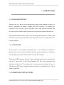
1. INTRODUCTION
1.1 PROBLEM DEFINITION
The basic idea is to develop a data acquisition & control system, wherein an effort is to made to standardize the Remote Terminal Unit (RTU) hardware. To encounter this problem the idea is to make a generic embedded device, which would be interfaced with the sensors on one side and would be attached to some kind of network on the other end. The problem definition for this project could be: Design and implement a system which enables the user to monitor and control sensors and similar devices in a remote field with a computer interface.
1.2 BACKGROUND
In this project we are primarily interfacing sensors to be controlled and monitored. Majority of the sensors used in the industry today have output specification as 4 to 20 mA, corresponding to the actual value of the data sensed by the transducer. The proposed RTU hardware functions as data acquisition unit thereby transmitting the data in its 'purest' form to the Control Terminal (CT). The data interpretation and calibration is done at the CT according to the sensor type and can be changed by the user. This makes the RTU generic enough to handle any kind of sensor falling in the 4 20 mA output specification.
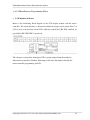
1.3CURRENT INDUSTRY PRACTICES
© Copyright 2004 Defense Research & Development Organization (DRDO), India
1
Embedded Network Client & Data Acquisition System
Currently the proprietary systems that exist in the industry are more hardware oriented and are specific to a given sensor. There are various implementations and standards proposed which can be used to build an RTU. But the major drawback of these systems is that they are not very generic and changing a single sensor may lead to changing the entire hardware unit.
Field buses link sensors and actuators at process level with the system intelligence i.e. with DCS systems, PLCs and controllers, so that the information they supply can flow into the factory information system. At the moment there is no standardized information system, which performs this task while at the same time being the part of the factory's wider information network. What does exist is largely based on the efforts of individual companies of interests groups. The aims of standardization are therefore twofold:
a. Instruments of various manufacturers must be able to operate on the same network, as is the case for the 4 to 20 mA interface, but using th full functionality of bidirectional digital communication.
b. There networks must be linked to production automation and commercial data processing systems such as MAP and Top so that, e.g. "Just in Time" material stocking and the tuning of output to actual order volume can be implemented.
1.4 OBJECTIVE & SCOPE
Objective of this project is to make a generic RTU that should be able to commute with the user over a network.
The scope of this project lies within the boundaries defined by the field instrumentation and the limitations imposed by the underlying hardware and the overall network systems and its subsystems.
© Copyright 2004 Defense Research & Development Organization (DRDO), India
2
Embedded Network Client & Data Acquisition System
1.5 PROPOSED WORK The work we propose is to build an embedded system (RTU) with fullfledged network stack to communicate with the CT. The sensors would be attached to this RTU and the user will be able to communicate (control / monitor) wit the sensors and actuators.
1.6 SPECIFICATIONS
1.6.1 Electrical Specifications
Supply Voltages (DC) a) RTU
: 5 V
b) Signal Conditioning Unit (SCU)
: + 12 V, 12 V
c) GSM modem : 3.3 V
1.6.2 Input Specifications
Input to the SCU must be in the range of 4 to 20 mA. This is specifically designed for interfacing generic sensors. Current implementation supports input for 4 sensors and controlled output for 4 actuators.
1.6.3 Software Specifications
Current implementation is a modest and scaled down version of UDP / IP stack. The Control Terminal Unit (CTU) has been implemented in Qt 3.0 environment under Linux. According to Qt manuals, this is portable to other platforms as well but not tested as such.
© Copyright 2004 Defense Research & Development Organization (DRDO), India
3
Embedded Network Client & Data Acquisition System
1.7 REQUIREMENTS
1.7.1 Hardware
Atmel AVR 90S8535 Microcontroller
Max 232 (RS 232 level shifter)
GSM Modem (Nokia 7110, Siemens MC35)
Dialup modem
© Copyright 2004 Defense Research & Development Organization (DRDO), India
4
Embedded Network Client & Data Acquisition System
1.7.2 Software
Codevision C Cross Compiler for AVR Microcontrollers
sP12 chip programming utility
AVR ASM32 assembler for AVR Microcontroller
AVR Studio simulator for AVR Microcontroller
GNU GCC
© Copyright 2004 Defense Research & Development Organization (DRDO), India
5
Embedded Network Client & Data Acquisition System
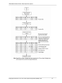
2. DESIGN ISSUE
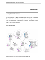
2. 1 REQUIREMENT ANALYSIS
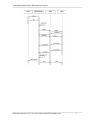
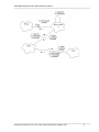
The basic requirement of DRDO was to make available the sensor data on the desktop. This could have been achieved in many ways. But to make the implementation more robust and nonproprietary, we decided to go by standards and implement the whole UDP / IP stack on the data source end. 2. 2 UML DIAGRAMS
© Copyright 2004 Defense Research & Development Organization (DRDO), India
6
Embedded Network Client & Data Acquisition System
© Copyright 2004 Defense Research & Development Organization (DRDO), India
7
Embedded Network Client & Data Acquisition System
© Copyright 2004 Defense Research & Development Organization (DRDO), India
8
Embedded Network Client & Data Acquisition System
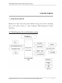
3. PROJECT DESIGN
3. 1 HARDWARE DESIGN
Hardware has ample share in the project. Hardware design, the most time consuming phase in the project, consists of: sensor interfacing, GSM interfacing and modem interfacing.
3.1.1 Block Diagram of the overall hardware system
© Copyright 2004 Defense Research & Development Organization (DRDO), India
9
Embedded Network Client & Data Acquisition System
Power Supply Unit
The power supply unit consists of stepdown transformers, bridge rectifier and filter and regulators that convert the voltage from the mains into the +/12V, 6V, 5V and 3.3V.
Signal Conditioning
The circuit provides the interface for up to four sensors having the standard 420mA outputs. This signal from the sensor is converted to 05V for ADC by using OpAmp signal conditioning. The calibration is done by span and zero adjustment.
Relay Interface & Control
The output control bus from the micro controller drives the relay circuitry. This circuit provides current amplification for driving relay coil. The optocoupler provides the isolation of the circuitry .The fourchannel control of the relay can be used to drive the actuators.
Micro controller Unit
The micro controller does all the processing of information, ADC and provides interface to peripherals. The data from the sensor interface circuit (05V) is converted to the digital form by programming the internal 10bit ADC. Now the task of micro controller is to transfer that data. Microcontroller programming consists of: sensor driver, GSM driver, modem driver, PPP implementation, UDP implementation, IP implementation and application layer implementation. It also provides the interface to peripherals like LCD, keypad and chip programmer. Implementing and programming the internal UART ports do serial communication. The on / off control to the relay is provided by reading the data packets from the end user. The data from the micro controller can be transferred to GSM © Copyright 2004 Defense Research & Development Organization (DRDO), India
10
Embedded Network Client & Data Acquisition System
by using Nokia FBus (Version 2) protocols and to the modem by implementing IP and UDP. The entire protocol stack is implemented in the micro controller. LCD and Keypad Interface
LCD provides the display of the field data and other related information. The connection and status information can also be viewed. The Keypad makes the LCD menu driven thus providing the basic functions like scrolling through the sensor data to selection of the transfer mode.
UART Multiplexing and Level Conversion
The micro controller provides only one serial asynchronous communication port. Now to communicate with more than two serial devices we have done multiplexing of the serial port. After selection of the device by controlling the multiplexer the Uart level is converted to RS232 standard so that it can be interfaced to the GSM module and dial up modem.
3.1.2 External Peripherals
LCD 16X2
Keypad 4 key
GSM Module (Nokia / Siemens)
Dial up Modem (Zoltrix)
© Copyright 2004 Defense Research & Development Organization (DRDO), India
11
Embedded Network Client & Data Acquisition System
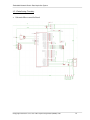
3.1.3 Interfacing Circuitry
•
Schematic Microcontroller Board
© Copyright 2004 Defense Research & Development Organization (DRDO), India
12
Embedded Network Client & Data Acquisition System
© Copyright 2004 Defense Research & Development Organization (DRDO), India
13
Embedded Network Client & Data Acquisition System
© Copyright 2004 Defense Research & Development Organization (DRDO), India
14
Embedded Network Client & Data Acquisition System
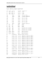
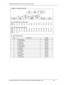
3.1.4 Bill Of Material
Signal conditioning and power supply board
Part Value Device Package Description D1 1N4004 1N4004 DO4110 DIODE D3 1N4004 1N4004 DO4110 DIODE D4 1N4004 1N4004 DO4110 DIODE D5 1N4004 1N4004 DO4110 DIODE IC1 DIL8 DIL08 Dual In Line IC2 78XXL 78XXL VOLTAGE REGULATOR IC3 78XXL 78XXL VOLTAGE REGULATOR IC4 DIL8 DIL08 Dual In Line IC5 DIL8 DIL08 Dual In Line IC6 DIL8 DIL08 Dual In Line IC7 DIL8 DIL08 Dual In Line IC8 DIL8 DIL08 Dual In Line IC9 DIL8 DIL08 Dual In Line IC10 DIL8 DIL08 Dual In Line IC11 78XXL 78XXL VOLTAGE REGULATOR K1 G5L G5L G5LE RELAY K2 G5L G5L G5LE RELAY K3 G5L G5L G5LE RELAY K4 G5L G5L G5LE RELAY OK2 4N37 4N37 DIL06 MOTOROLA OPTO COUPLER OK3 4N37 4N37 DIL06 MOTOROLA OPTO COUPLER OK4 4N37 4N37 DIL06 MOTOROLA OPTO COUPLER OK5 4N37 4N37 DIL06 MOTOROLA OPTO COUPLER Q2 BC547 BC547 TO92 NPN Transistor Q3 BC547 BC547 TO92 NPN Transistor Q4 BC547 BC547 TO92 NPN Transistor Q5 BC547 BC547 TO92 NPN Transistor R1 RTRIMM64W RTRIM64W Trimm resistor R2 RUS_0207/10 0207/10 RESISTOR, American symbol
R3 RUS_0207/10 0207/10 RESISTOR, American symbol
R4 RUS_0207/10 0207/10 RESISTOR, American symbol
R5 RUS_0207/10 0207/10 RESISTOR, American symbol
R6 RUS_0207/10 0207/10 RESISTOR, American symbol
R7 RUS_0207/10 0207/10 RESISTOR, American symbol
R8 RUS_0207/10 0207/10 RESISTOR, American symbol
R9 RUS_0207/10 0207/10 RESISTOR, American symbol
R10 RUS_0207/10 0207/10 RESISTOR, American symbol
R11 RUS_0207/10 0207/10 RESISTOR, American symbol
R12 RUS_0207/10 0207/10 RESISTOR, American symbol
R13 RUS_0207/10 0207/10 RESISTOR, American symbol
R14 RUS_0207/10 0207/10 RESISTOR, American symbol
R15 RUS_0207/10 0207/10 RESISTOR, American symbol
R16 RTRIMM64W RTRIM64W Trimm resistor R17 RUS_0207/10 0207/10 RESISTOR, American symbol
R18 RUS_0207/10 0207/10 RESISTOR, American symbol
R19 RUS_0207/10 0207/10 RESISTOR, American symbol
R20 RTRIMM64W RTRIM64W Trimm resistor R21 RUS_0207/10 0207/10 RESISTOR, American symbol
R22 RUS_0207/10 0207/10 RESISTOR, American symbol
R23 RTRIMM64W RTRIM64W Trimm resistor R24 RUS_0207/10 0207/10 RESISTOR, American symbol
R25 RTRIMM64W RTRIM64W Trimm resistor © Copyright 2004 Defense Research & Development Organization (DRDO), India
15
Embedded Network Client & Data Acquisition System
R26 RUS_0207/10 0207/10 RESISTOR, American symbol
R27 RUS_0207/10 0207/10 RESISTOR, American symbol
R28 RUS_0207/10 0207/10 RESISTOR, American symbol
R29 RTRIMM64W RTRIM64W Trimm resistor R30 RUS_0207/10 0207/10 RESISTOR, American symbol
R31 RTRIMM64W RTRIM64W Trimm resistor R32 RUS_0207/10 0207/10 RESISTOR, American symbol
R33 RUS_0207/10 0207/10 RESISTOR, American symbol
R34 RUS_0207/10 0207/10 RESISTOR, American symbol
R35 RTRIMM64W RTRIM64W Trimm resistor R36 RUS_0207/10 0207/10 RESISTOR, American symbol
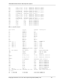
SV2 S10P S10P AMP MT CONNECTOR SV3 S05P S05P AMP MT CONNECTOR SV4 S12P S12P AMP MT CONNECTOR SV5 S08P S08P AMP MT CONNECTOR SV6 S04P S04P AMP MT CONNECTOR Microcontroller board
Part Value Device Package Description C1 CAPNP5 C5 C2 CAPNP5 C5 C3 ELC2,5 ES2,5 C4 ELC2,5 ES2,5 C5 ELC2,5 ES2,5 C6 ELC2,5 ES2,5 C7 CAP5 C5 C8 ELC2,5 ES2,5 C9 CAP5 C5 CON2 CON40 CON40 CONNECTOR D1 1N4004 1N4004 DO4110 DIODE D2 1N4004 1N4004 DO4110 DIODE D3 1N4004 1N4004 DO4110 DIODE D4 1N4004 1N4004 DO4110 DIODE D5 1N4004 1N4004 DO4110 DIODE D6 ZENERDIODEDO41Z10 DO41Z10 ZDiode D7 DIODE2,5 D2,5 IC1 AT90S8535P AT90S8535P DIL40 MICROCONTROLLER IC2 DIL16 DIL16 Dual In Line IC3 DIL16 DIL16 Dual In Line Q1 XTAL/S QS CRYSTAL R2 RUS_0204/5 0204/5 RESISTOR, American symbol R3 RUS_0207/10 0207/10 RESISTOR, American symbol R4 RTRIMM64W RTRIM64W Trimm resistor SV1 S05P S05P AMP MT CONNECTOR SV2 S10P S10P AMP MT CONNECTOR SV3 S05P S05P AMP MT CONNECTOR SV4 S16P S16P AMP MT CONNECTOR SV5 S08P S08P AMP MT CONNECTOR SV6 S02P S02P AMP MT CONNECTOR SV7 S06P S06P AMP MT CONNECTOR T1 2N706 2N706 TO18 NPN TRANSISTOR U$2 CHIPCARDISO7816 CHIPCARDISO7816 ISO7816 Chip card connector ISO 7816
X1 20FLZSM1 20FLZSM1 20FLZSM CONNECTOR X2 20FLZSM1 20FLZSM1 20FLZSM CONNECTOR © Copyright 2004 Defense Research & Development Organization (DRDO), India
16
Embedded Network Client & Data Acquisition System
X3 F09H F09H SUBD X5 F09H F09H SUBD © Copyright 2004 Defense Research & Development Organization (DRDO), India
17
Embedded Network Client & Data Acquisition System
3. 2 SOFTWARE DESIGN
Software design has been divided into two parts, namely Microcontroller programming and Graphical User Interface (GUI) programming. Microcontroller programming is a major part of the project where all the networking protocols and sensorinterfacing is done.
3.2.1 Microcontroller Programming
The microcontroller used is Atmel AVR 90S8535. The AVR core combines a rich instruction set with 32 generalpurpose working registers. All the 32 registers are directly connected to the Arithmetic Logic Unit (ALU), allowing two independent registers to be accessed in one single instruction executed in one clock cycle. The resulting architecture is more code efficient while achieving throughputs up to ten times faster than conventional CISC microcontrollers.
The AT90S8535 provides the following features: 8K bytes of InSystem Programmable Flash, 512 bytes EEPROM, 512 bytes SRAM, 32 generalpurpose I/O lines, 32 general
purpose working registers, flexible timer/counters with compare modes, internal and external interrupts, a programmable serial UART, programmable Watchdog Timer with internal oscillator, an SPI serial port and two softwareselectable powersaving modes. The Idle Mode stops the CPU while allowing the SRAM, timer/counters, SPI port and interrupt system to continue functioning. The Powerdown Mode saves the register contents but freezes the oscillator, disabling all other chip functions until the next external interrupt or hardware reset. AT90S8535 features include inbuilt UTC and a 10bit ADC with 8 channels.
The AVR uses a Harvard architecture concept – with separate memories and buses for program and data. The program memory is executed with a twostage pipeline. While one © Copyright 2004 Defense Research & Development Organization (DRDO), India
18
Embedded Network Client & Data Acquisition System
instruction is being executed, the next instruction is prefetched from the program memory. This concept enables instructions to be executed in every clock cycle. The program memory is InSystem Programmable Flash memory.
The device is manufactured using Atmel’s highdensity nonvolatile memory technology. The onchip InSystem Programmable Flash allows the program memory to be reprogrammed insystem through an SPI serial interface or by a conventional nonvolatile memory programmer. By combining an enhanced RISC 8bit CPU with InSystem Programmable Flash on a monolithic chip, the Atmel AT90S8535 is a powerful micro controller that provides a highly flexible and cost effective solution to many embedded control applications.
The AT90S8535 AVR is supported with a full suite of program and system development tools including: C compilers, macro assemblers, program debugger/simulators, incircuit emulators and evaluation kits.
Microcontroller programming consists of: sensor driver, GSM driver, modem driver LCD driver, PPP implementation, UDP implementation, IP implementation and application layer implementation. 3.2.1.1 Sensor Driver The sensor driver circuit is elaborated in the previous section, which comprises of signal conditioning (IV) unit, where by the analog voltage is fed to the inbuilt ADC within the microcontroller. Whenever the system is requested for the data from the desired channel it’s actually a simple A to D conversion of the analog signal at input channel 0 of the microcontroller. Then the sensor driver software is responsible for the proper functioning of the ADC. The special function register (SFR) ADMUX is set to input channel number and as for the start of conversion we set SFR ADCSR| = x040. On the completion of conversion the data is available in register ADCW, which is a 10bit value.
© Copyright 2004 Defense Research & Development Organization (DRDO), India
19
Embedded Network Client & Data Acquisition System
The ADC ISR (interrupt [ADC_INT] void adc_isr(void)) comes in to picture when the EOC is signaled.
As for the actuator again the major role to be played is the hardware for the control circuitry as detailed in the previous section. The driver software has but little burden just to pass control to the relay thereby driving the actuator. A simple port IO comes to play when the request is made to the system.
3.2.1.2 Modem Driver
Modem driver software is a program that initializes the modem at proper baud rate and then places a call to the ISP. This driver mainly features functions related to the modem control by implementing standard “AT” commands. The interface is a scaled down version of RS232 using 3wire connection. Unless the DTR & RTS are pulled low the modem is not going to function properly so the hardware is designed so as to meet the above requirements. All the communications with the modem is done through the micro
controller UART. The baud rate is set by putting appropriate values in the UBRR register (refer MISC. programming notes for details), and serial communications is provided by primitives putchar() / getchar() to send and receive a single byte.
3.2.1.3 GSM Driver Apart from the standard AT commands there are special/extended set of at commands for the GSM modems, most of which are preparatory. However the main purpose of this driver is to send and receive SMS.
Placing a data call through a GSM modem is out of the question. The GSM driver implementation has come in two different flavors:
Implementation of AT+C commands
© Copyright 2004 Defense Research & Development Organization (DRDO), India
20
Embedded Network Client & Data Acquisition System
Implementation of proprietary Nokia FBUS/MBUS protocols Implementation of the former is much similar to the Modem driver as the only thing required was to deal with the proper AT+C command. The sequences of functions were designed to initialize the modem in text mode rather than dealing in the PDU (protocol data unit) mode followed by functions to send and receive SMS. Note: we have specific AT+C commands for the primitives such as read/delete SMS and like…
While the programming for GSM driver using the AT+C commands was not only easy but efficient, however the discovery was a bit delayed, it was the FBUS/MBUS Nokia protocols that were cracked first. Thanks goes to the gnokii (http://www.gnokii.org/) team for figuring out the frame format, among many other things. Although this driver was written from scratch, it was heavily based on their research.
The driver contains a set of functions for sending and receiving SMS (short message service) text messages across a GSM network with a Nokia 51xx series phone. We have only tested it with Nokia 5110 handset, however it should work fine with any GSM phone in the series. It should also work with the 3310 phones. These functions were meant to be as portable as possible (they contain no serial communications code), and to perform two simple things: send and receive SMS. This code was meant to be small, so that it could be used in our system. To use setup the serial port and call init(). Then use smssend() and smsrecv() to send/receive SMS messages. All incoming SMS messages are deleted from the phone's inbox.
© Copyright 2004 Defense Research & Development Organization (DRDO), India
21
Embedded Network Client & Data Acquisition System
3.2.1.4 PPP Implementation The PointtoPoint Protocol (PPP) provides a standard method for transporting multi
protocol datagrams over pointtopoint links. PPP is comprised of three main components: A method for encapsulating multiprotocol datagrams. A Link Control Protocol (LCP) for establishing, configuring, and testing the datalink connection. A family of Network Control Protocols (NCPs) for establishing and configuring different networklayer protocols.
The PPP connection can be broken into several phases. First, establishment phase uses Link Control Protocol (LCP) to detect and negotiate link options with the remote computer. Next the authentication phase verifies the User ID and password with Password Authentication Protocol (PAP). Although not one of the phases, this is where ISPs negotiate compression protocols. The final phase is the network layer protocol. Each protocol such as IP, is configured with its control protocol like IPCP. Control protocols are very similar for LCP, PAP, CCP, and IPCP but the protocol field is different and the options have different meanings. Each packet can request, deny, or accept a list of options. Negotiation starts with either side requesting a list of options in a request (REQ) packet. Each option consists of an © Copyright 2004 Defense Research & Development Organization (DRDO), India
22
Embedded Network Client & Data Acquisition System
option type byte, length byte, and option parameters. If the receiving end likes all the options, it replies with an acknowledge packet (ACK).
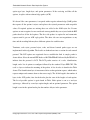
If it doesn’t like some parameters, it responds with a negative acknowledge (NAK) packet that repeats all the options it rejects and replaces the rejected parameters with acceptable values. If required options are missing those are added to the NAK reject list. If some options are not recognized or are considered nonnegotiable they are rejected with the REJ packet that lists all the bad options. The first side updates its option list and retransmits requests until it gets an ACK reply packet. The other side can start negotiations at any time and the resulting link may have different options for each direction. Terminate, code reject, protocol reject, echo, and discard control packet types are not implemented in this algorithm. The details are broken down into a section for each control protocol. The LCP options are negotiated first to establish the link. A sample packet is shown below. It has the normal PPP header of 0x7E 0xFF 0x03 followed by 0xC0 0x21 to indicate that the protocol is LCP. The LCP packet consists of a code, identification, length, and a list of options to configure followed by the standard 2 byte PPP CRC. The code is a byte to indicate the meaning of the packet. A list of codes is found in the Table shown. The identification byte is incremented after each negotiation request, which makes requests unique and connects them to the correct reply. The 16bit length is the number of bytes in the LCP packet, four for the header plus the sum of the lengths of each option. The list of possible options is again found in Table. Each option is sent as a onebyte option type, followed by a onebyte option length, and an optional parameter. The option length is two for the option header plus the number of bytes in the parameter.
© Copyright 2004 Defense Research & Development Organization (DRDO), India
23
Embedded Network Client & Data Acquisition System
© Copyright 2004 Defense Research & Development Organization (DRDO), India
24
Embedded Network Client & Data Acquisition System
•
PAP OPTIONS
The PAP details can be found in RFC 1334. For this algorithm they were simplified to one packet exchange. The PAP packet is similar to LCP with 0xC023 instead of 0xC021 in the protocol field. Instead of negotiating options, only the User ID and password are sent as a request. If the server acknowledges, then the user is logged in. A NAK reply would mean that the User ID or password is incorrect. The format can be seen in figure shown. The first payload byte is the length of the User ID, followed by the User ID. The password is appended in the same way: Length first followed by password.
•
IPCP OPTIONS
After LCP is negotiated and PAP is accepted, the Internet Protocol must be configured. The options are for IP address and IP Compression with more details in RFC 1332. IP address is option three and its 4byte parameter is the Internet address of this node. The server typically sends a request with option three followed by the IP address. Otherwise, the address is found by requesting an invalid choice like 0.0.0.0 and the server replies with a NAK and option three with the correct address. A sample packet is shown below. Some server implementations may request IP Compression Protocol option type two. These requests are rejected because TCP is not implemented in this algorithm. © Copyright 2004 Defense Research & Development Organization (DRDO), India
25
Embedded Network Client & Data Acquisition System
•
CCP OPTIONS
Some servers will try to negotiate compression, but since this algorithm is optimized for size instead of speed, these requests are rejected. The compression algorithms are complex and in some cases proprietary, yet have little benefit on the short packets used in this algorithm. Choosing the puddle jumper option type 3 means that no compression or decompression is required.
© Copyright 2004 Defense Research & Development Organization (DRDO), India
26
Embedded Network Client & Data Acquisition System
3.2.1.5 UDP Implementation Its simplicity and bandwidth efficiency make it an important part of some multimedia Internet protocols. This project supports UDP protocol as we had limited amount of memory on chip.
First of all UDP is an unreliable protocol, not that it should be avoided, but rather that packets can get lost without warning and may require retransmission. It is deterministic in the sense that each packet, or timeout, triggers the next event without regard to what state the connection is in. This simplifies programming and makes debugging much easier. There are 20 bytes of IP header, then 8 bytes of UDP header, and the UDP data. The first two 2 byte fields are the source and destination port numbers. The port numbers are important to identify what process gets the UDP data. The next two bytes are the UDP length, eight bytes of UDP header plus the length of the UDP data. This value is redundant because it can be calculated from the IP header by subtracting the header length from the total length. The last 2 bytes of the UDP header are the 16 bit one’s complement checksum of the pseudo header, the UDP header, and the UDP data. The pseudo header is not transmitted but the following 12 bytes are added to the checksum anyway. The 32 bit source and destination addresses, the 16bit UDP address, and the 8bit protocol field are extended to 16 bits to ensure that the UDP data is going to the correct IP address. The checksum is optional and set to zero if not used. Since zero means no checksum, then a valid checksum that adds up to zero must be inverted to 0xFFFF. If the UDP data is an odd number of bytes, your 16 bit checksum routine will need to pretend that there is an extra byte 0x00 at the end.
The format of the UDP data will depend on which port you are connecting to and which protocol is using the data.
© Copyright 2004 Defense Research & Development Organization (DRDO), India
27
Embedded Network Client & Data Acquisition System
The IP Packet Format
3.2.1.6 IP Implementation
The Internet Protocol is designed for use in interconnected systems of packetswitched computer communication networks. The internet protocol provides for transmitting blocks of data called datagrams from sources to destinations, where sources and destinations are hosts identified by fixed length addresses. The internet protocol also provides for fragmentation and reassembly of long datagrams, if necessary, for transmission through "small packet" networks.
The internet protocol uses four key mechanisms in providing its service: Type of Service
© Copyright 2004 Defense Research & Development Organization (DRDO), India
28
Embedded Network Client & Data Acquisition System
Time to Live
Options
Header Checksum
The Type of Service is used to indicate the quality of the service desired. The type of service is an abstract or generalized set of parameters which characterize the service choices provided in the networks that make up the internet. This type of service indication is to be used by gateways to select the actual transmission parameters for a particular network, the network to be used for the next hop, or the next gateway when routing an internet datagram. The Time to Live is an indication of an upper bound on the lifetime of an internet datagram. It is set by the sender of the datagram and reduced at the points along the route where it is processed. If the time to live reaches zero before the internet datagram reaches its destination, the internet datagram is destroyed. The time to live can be thought of as a self destruct time limit. The Options provide for control functions needed or useful in some situations but unnecessary for the most common communications. The data may contain errors. If the header checksum fails, the internet datagram is discarded at once by the entity which detects the error.
The internet protocol does not provide a reliable communication facility. There are no acknowledgments either endtoend or hopbyhop. There is no error control for data, only a header checksum. There are no retransmissions. There is no flow control. Errors detected may be reported via the Internet Control Message Protocol (ICMP), which is implemented in the internet protocol module. © Copyright 2004 Defense Research & Development Organization (DRDO), India
29
Embedded Network Client & Data Acquisition System
3.2.1.7 FBUS Implementation
MBus, FBus’ predecessor, is a one pin bidirectional bus for both transmitting and receiving data from the phone. It is slow (9600bps) and only halfduplex. Only two pins on the phone are used. One ground and one data. MBus runs at 9600bps, 8 data bits, odd parity, one stop bit. The data terminal ready (DTR) pin must be cleared with the request to send (RTS). This powers the electronics in the cable and I think it sets it for MBus operation.
FBus is the later highspeed fullduplex bus. It uses one pin for transmitting data and one pin for receiving data plus the ground pin. Very much like a standard serial port. It is fast 115,200bps, 8 data bits, no parity, one stop bit. For FBus the data terminal ready (DTR) pin must be set and the request to send (RTS) pin cleared. •
The FBus Protocol and Commands
The FBus is bidirectional serial type bus running at 115,200bps, 8 data bits. The serial cable contains electronics for level conversion and therefore requires power. The first thing to do is supply power to the cable electronics and this is done by setting the DTR (Data Terminal Ready) pin and clearing the RTS (Request to Send) pin. The next step is to synchronize the UART in the phone with your PC or microprocessor. This is done by sending a string of 0x55 or 'U' 128 times. Simple hay! The bus is now ready to be used for sending frames. The Nokia protocol has a series of commands that allow the user to make calls, send and get SMS messages and lots more.
© Copyright 2004 Defense Research & Development Organization (DRDO), India
30
Embedded Network Client & Data Acquisition System
Frame format for FBUS version 1
{ FrameID, FrameLength, MsgType, {block}, SeqNo, ChkSum }
where FrameID: 0x01 Command frame from computer to Nokia 0x02xxx Data call frame from computer to Nokia xxx
0x03 Data call frame from Nokia to computer 0x04 Command frame from Nokia to computer FrameLength: {block} + 2
MsgType: see list
SeqNum: Sequence number of command in case where direction is from ME to computer, the sequence number is counting from 0x30 to 0x37 and resetting back to 0x30. When direction is from computer to ME, sequence number counts from 0x08 to 0x0f and resets back to 0x08. It may not be required to be this way. Sequence numbers are used in acknowledging commands.
ChkSum1: CRC = 0;
for (i = 0; i < (2 + CMD_LEN); i++)
CRC ^= frame[i];
Frame format for FBUS version 2/Direct IRDA
{ FrameID, DestDEV, SrcDEV, MsgType, 0x00, FrameLength, {block}, FramesToGo,
SeqNo, PaddingByte, ChkSum1, ChkSum2 }
where FrameID: 0x1c: IR / FBUS
0x1e: Serial / FBUS
DestDev, SrcDev: 0x00: mobile phone
0x0c: TE (FBUS) [eg. PC]
MsgType: 0x02: SMS handling
s Send SMS message { 0x0001, 0x02, 0x00 (SEND REQUEST)}
r Message sent { 0x0002 }
© Copyright 2004 Defense Research & Development Organization (DRDO), India
31
Embedded Network Client & Data Acquisition System
r Send failed { 0x0003, ?, ?, error (code)} s Get SMS message { 0x0007, 0x02, location, 0x01, 0x64 }
s Initiate connection { 0x000d, 0x00, 0x00, 0x02 }
r Initiate ACK { 0x000e, 0x01 }
r SMS message received { 0x0010, ...... } (whole message)
FrameLength: {block} + 2 (+ 1 if PaddingByte exists)
FramesiToGo: 0x01 means the last frame
SeqNo: [0xXY]
X: 4: first block
0: continuing block
Y: sequence number
PaddingByte: 0x00 if FrameLength would be an odd number anyways it doesn't exists.
•
SMS PointtoPoint Character Packing GSM 03.38 Alphabets and Language Specific Format is the technical specification that describes the packing of 7bit characters and shows the standard character map. Packing ASCII into 7bit characters is a pain, but is quite easy to do. Here is a quick example. Let's say we want to decode the string 'hello'. First 'hello' is displayed in hexadecimal using the character map provided in GSM 03.38. For A to Z and numbers it is just the standard ASCII conversion.
h e l l o (ASCII characters)
68 65 6C 6C 6F (In hexadecimal)
1101000 1100101 1101100 1101100 1101111 (In Binary)
When dealing with binary, it makes life easier to write everything backwards. The first byte in the string is on the right. The least significant bit is then displayed on the left with © Copyright 2004 Defense Research & Development Organization (DRDO), India
32
Embedded Network Client & Data Acquisition System
the most significant bit on the left. Shown below is the same string of 'hello' just displayed backwards. Then it's just a matter to dividing the binary values into bytes starting with the first character in the string. (Start from right and go to left.) The first decoded byte is simply the first 7 bits of the first character with the first bit of the second character added to the end as shown below. The next decoded byte in then the remaining 6 bits from the second character with two bits of the third byte added to the end. This process just keeps going until all characters are decoded. The last decoded byte is the remaining bits from the last character with the most significant bits packed with zeros.
6F
6C
6C
65
68
1101111 1101100 1101100 1100101 1101000 (The ASCII characters shown in binary)
110 11111101 10011011 00110010 11101000 (The above binary just split into 8 bit segments)
06 FD
9B
32
E8
(The 8 bit segments decoded into hex)
The message hello is therefore E8 32 9B FD 06 when packed. When playing with sending SMS messages a lot of decoding is required. Therefore we wrote a few small programs to automatically pack and unpack the data.
3.2.1.8 Application Layer Implementation
The job of the application program running inside the embedded host is to provide the sensor data to the request coming to it via modem or GSM network. For this the application continuously polls the incoming packets from the dialup lines and from the GSM network. The application is prepared to respond to the requests, which are in a specific format. The format typically is: $REQ$. Here REQ is to be replaced by the data to be retrieved. On receiving the request, the host retrieves the data and replies back. On a dialup connection © Copyright 2004 Defense Research & Development Organization (DRDO), India
33
Embedded Network Client & Data Acquisition System
the host replies back with a UDP packet whereas for a request on GSM network, the host replies via SMS.
Examples:
$DATA1$
to retrieve the data from sensor 1
$DATA2$
to retrieve the data from sensor 2
© Copyright 2004 Defense Research & Development Organization (DRDO), India
34
Embedded Network Client & Data Acquisition System
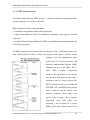
3.2.1.9 Miscellaneous Programming Notes
•
LCD Interface & Driver
Below is the interfacing block diagram of the LCD display module with the micro
controller. The actual interface is shown in the hardware design section, where Port C of 8535 is used as the data bus for the LCD, while the control lines (RS, RW, enabled) are provided by PD.5 PD.6 PD.7 respectively.
The software associated for driving the LCD is greatly adopted from the method as illustrated in textbook by Gaonkar. Following are the notes that further elucidate the microcontroller programming for LCD.
© Copyright 2004 Defense Research & Development Organization (DRDO), India
35
Embedded Network Client & Data Acquisition System
© Copyright 2004 Defense Research & Development Organization (DRDO), India
36
Embedded Network Client & Data Acquisition System
© Copyright 2004 Defense Research & Development Organization (DRDO), India
37
Embedded Network Client & Data Acquisition System
•
8535 Programming Notes
I/O Ports
All AVR ports have true readmodifywrite functionality when used as general digital I/O ports. This means that the direction of one port pin can be changed without unintentionally changing the direction of any other pin with the SBI and CBI instructions.
The same applies for changing drive value (if configured as output) or the enabling/disabling of pullup resistors (if configured as input).
Three I/O memory address locations are allocated for each Port one each for the Data Register PORTx, Data Direction Register – DDRx and the Port x Input Pins – PINx. The Port x Input Pins address is readonly, while the Data Register and the Data Direction Register are read/write.
UART Programming
As per the 8535 data sheet, the AT90S8535 features a full duplex (separate receive and transmit registers) Universal Asynchronous Receiver and Transmitter (UART). The main features are:
• Baud rate generator that can generate a large number of baud rates (bps)
• High baud rates at low XTAL frequencies
• 8 or 9 bits data
• Noise filtering
• Overrun detection
• Framing Error detection
• False Start Bit detection
• Three separate interrupts on TX Complete, TX Data Register Empty and RX Complete
One of the striking reasons for choosing AVR microcontroller was its inbuilt programmable UART and its ease of programming, although using a crosscompiler hides © Copyright 2004 Defense Research & Development Organization (DRDO), India
38
Embedded Network Client & Data Acquisition System
the complexity that arises in assembly programming, it certainly helped until a suitable crosscompiler was finalized i.e. Code Vision. Most of the initial programming was done in assembly using AVR Studio4. The prominent I/O Registers that deal with UART programming are UBRR, UDR, and USR&UCR.
The standard C language I/O functions were adapted to work on embedded micro
controllers with limited resources.
The lowest level Input/Output function(s) are:
char getchar(void) returns a character received by the UART, using polling.
void putchar(char c) transmits the character c using the UART, using polling.
Prior to using these functions you must:
• Initialize the UART's Baud rate
• Enable the UART transmitter
• Enable the UART receiver.
Example:
#include <90s8515.h>
#include <stdio.h>
/* quartz crystal frequency [Hz] */
#define xtal 4000000L
/* Baud rate */
#define baud 9600
void main(void) {
char k;
/* initialize the UART's baud rate */
UBRR = xtal / 16 / baud 1;
/* initialize the UART control register
RX & TX enabled, no interrupts, 8 data bits */
UCR = 0x18;
while (1) {
/* receive the character */
k = getchar();
/* and echo it back */
putchar(k);
}
}
© Copyright 2004 Defense Research & Development Organization (DRDO), India
39
Embedded Network Client & Data Acquisition System
All the high level Input/Output functions use getchar and putchar.
© Copyright 2004 Defense Research & Development Organization (DRDO), India
40
Embedded Network Client & Data Acquisition System
3. 3 IMPLEMENTATION ASPECTS
The initial aim of the project was to build an embedded data acquisition system that would terminate on LAN using Ethernet LAN controller CS 8900A. The major problems faced using the CS 8900A were that the chip is not readily available and is expensive. Though this being our primary goal, the system our client (DRDO) needed was just a mechanism for remote data retrieval and monitoring. So to meet the basic requirements we went on to implement the system using dialup modem and the EPBAX system that currently exists in the client’s premises.
Another challenge put forward by our client is to make the system generic enough so as to interface with any sensor. The answer to this has been explained in the hardware design. Another trivial looking major modification was to make calibration of the sensor data flexible and changeable by the user as and when attached sensors changes. This is achieved by providing an extensive user interface.
Dialup connection imposes its own drawbacks like: one line has to be dedicated, and the line has to be up, or has to be up whenever required. These conditions may not be met every time and hence some other means had to be there to access the data during emergency. To address these issues a major revamping of the project was done and GSM module implementation, interfacing and its driver along with the specific protocols for the hardware were incorporated in to the project. © Copyright 2004 Defense Research & Development Organization (DRDO), India
41
Embedded Network Client & Data Acquisition System
4. USER MANUAL
4.1 OPERATING PROCEDURE
The embedded host operates in two modes. One is over UDP/IP and other is over GSM network.
4.1.1 Operations over UDP / IP
The monitor tool, montoo when started, tries to connect to the embedded web host using ARP. It contains the MAC address of the host and locates its IP address. When connected, the host authenticates the user and waits for the request. On request of user, montoo sends request command to the host and retrieves data. The timetolive, or the time montoo waits for the answer is around 15 seconds after which it reports the user about the disconnection. If it gets the requested data within 15 seconds, it shows he value as well as graph to the user. Montoo operates over UDP / IP and sends request packets after every time interval which can be adjusted by the user.
4.1.2 Operations over GSM
With any mobile phone operating over GSM network can retrieve data from the embedded web host using Short Messaging Service (SMS). For retrieving data of sensor 1, send an SMS to the web host number with text: “$DATA1$”. On receiving this SMS, the embedded web host would respond to the sender with the data of sensor 1 via SMS. © Copyright 2004 Defense Research & Development Organization (DRDO), India
42
Embedded Network Client & Data Acquisition System
This facility is specifically provided for the situations where the user may not have access to the monitoring tool or Internet. This facility is helpful for retrieving data on the move. © Copyright 2004 Defense Research & Development Organization (DRDO), India
43
Embedded Network Client & Data Acquisition System
5. CONCLUSION
5.1 DEVELOPERS COMMENTS
The project did work out as expected. But the major thing that should be appreciated is the GSM interfacing, network protocol stack (UDP / IP) implementation, FBUS protocol implementation and everything at microcontroller level. This project exposed us to many new arenas of engineering and especially computer filed. The new thing to learn from the project (apart from syllabus) is the embedded environment programming. Other values we got from the project is working as a team member and bringing out some collective output.
5.2 FUTURE ENHANCEMENTS
Though few drawbacks exists in the system, the source of which is primarily dialup connection and the limitations that come along with it; most of them could be removed by the use of Ethernet LAN controller. Software for the network controller remains exactly same and only additional driver for LAN controller needs to be written.
Applications of the product as a whole are immense, web based router and firewall configuration to name a few, but can be enhanced further by incorporating HTTP over TCP, which were not implemented due to memory constraints.
At present the microcontroller programming has been done right from the scratch using a C cross compiler. Therefore the efficiency of the system as a whole could not be © Copyright 2004 Defense Research & Development Organization (DRDO), India
44
Embedded Network Client & Data Acquisition System
compared with any existing system. This could be ‘standardized’ by using standard real time operating system like RTLinux, Vxworks or alike.
© Copyright 2004 Defense Research & Development Organization (DRDO), India
45
Embedded Network Client & Data Acquisition System
6. BIBLIOGRAPHY
•
Atmel 8535 data sheet http://www.atmel.com/
•
Atmel Application notes http://www.atmel.com/
•
Embedded Ethernet http://www.embeddedethernet.com/ •
Help manuals of Code Vision http://www.infotech.ir.ro/
•
W.R. Stevens, TCP/IP Illustrated, Vol. 1, Addison Wesley, Reading, MA, 1994
•
RFC 0768 User Datagram Protocol. J. Postel. Aug281980.
•
RFC 0791 Internet Protocol. J. Postel. Sep011981.
•
RFC 1071 Computing the Internet checksum. R.T. Braden, D.A. Borman, C. Partridge. Sep011988.
•
RFC 1332 The PPP Internet Protocol Control Protocol (IPCP). G. McGregor.May 1992.
•
RFC 1334 PPP Authentication Protocols. B. Lloyd, W. Simpson. October 1992.
•
RFC 1570 PPP LCP Extensions. W. Simpson. January 1994.
•
RFC 1661 The PointtoPoint Protocol (PPP). W. Simpson, Editor. July 1994.
•
RFC 1663 PPP Reliable Transmission. D. Rand. July 1994.
•
GSM 03.38 Alphabets and languagespecific information. http://webapp.etsi.org/key/queryform.asp
•
The Linux Gnokii Project – http://www.gnokii.org/
•
Wayne Peacock’s Homepage http://users.senet.com.au/~wpeacock/
© Copyright 2004 Defense Research & Development Organization (DRDO), India
46
Embedded Network Client & Data Acquisition System
RFCs available online from sites like: http://www.cis.ohiostate.edu/hypertext/information/rfc.html
Assigned PPP Numbers: ftp://ftp.isi.edu/innotes/iana/assignments/pppnumbers
© Copyright 2004 Defense Research & Development Organization (DRDO), India
47
Embedded Network Client & Data Acquisition System
7. REFERENCES
Mr. S. C. Sati, Scientist ( E Grade ), DRDO, Dighi, Pune.
Dr. N. C. Jain, Senior faculty, D.Y.P.C.O.E., Pune.
Mr. Amol Bidve, Developer & VLSI Designer, ST Microelectronics, Noida.
Mr. Anuj Kumar, CTO, LevelE Tektics, Pune. Prof. Leet, Professor at University of Cleveland, Ohio, USA.
© Copyright 2004 Defense Research & Development Organization (DRDO), India
48