1
ATasicICE
Designer Guide
June 1998
ATasicICE
Designer Guide
1.0
Introduction
The AVR ATasicICE (ASIC ICE) is a standardized development and test platform for
users of AVR in ASICs. The solution provides a flexible way of real time emulation of the
ASIC at hand. The ASIC ICE system is based on AVR Core version 2, which handles up
to 128K bytes (64K x 16 bit) program memory and 64K bytes data memory.
The ASIC ICE package also includes the ATasicICE POD as a reference pod design.
This document describes how to interface the ATasicICE with custom pod designs. Two
example designs based on the ATasicICE POD are also presented. For further information about the ASIC ICE Pod, see the document ICEPRO ASIC POD User’s Guide. The
ASIC ICE is used together with the AVR Studio™ software.
1.1
Description of
the ASIC ICE
ASIC ICE is based on the well proven AVR ICEPRO platform which is used for emulation of AVR standard parts. However, as each ASIC project has specific needs, a more
flexible solution has been developed. The main difference between the standard Emulator and the ASIC ICE Emulator is that all the necessary buses as well as the interrupt
system are reflected on the pod connector.
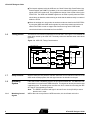
Figure 1-1. AVR ATasicICE, Block Diagram
AVR ATASICICE
DBUS
CLOCK
GENERATION
LOGIC
AVR V2 CORE
ADR
HOST
INTERFACE
CTRL
HOST PC
W/ AVR
STUDIO
PROGRAM
MEMORY
INTERNAL
DATA
MEMORY
POD INTERFACE
POD
The AVR V2 Core is implemented in a high speed gate-array. Maximum operating frequency for the core is currently higher than possible for the rest of the emulator system.
Timing issues are discussed in a separate section. The pod interface operates on +5V
only. Both program memory and internal data memory are mapped into an overlay
ATasicICE Designer Guide
1
ATasicICE Designer Guide
memory. This makes it easy to download programs from the host. The clock generation
logic is controlled by the emulator, but additional lines to and from the pod interface
makes external control possible.
Note:
1.2
Clock System
Since the I/O is placed on an external pod, the timing will be different from the
timing in a final ASIC. Additional delay should be calculated into the total signal
delay. This delay includes the line delays.
Using the AVR Studio™ software front end, the user can select between the on-board
emulator clock, or an external clock source, e.g. the target system clock. EXTCLKEN
indicates whether an external clock source is expected or not, and EXTCLKIN is the
input pin for external clock source when selected.
Note:
The pod should never try to drive EXTCLKIN if the EXTCLKEN is inactive.
The on-board clock module is functionally equivalent to the Verilog description:
assign clkalways = ck;
assign clkosc
= ck | ~clken;
assign ckcore
= stopcore | clkosc;
assign clkio
= clkrun ? stopio | clkosc: emiowr;
ck is the clock source (internal or external). ckcore is the clock source for the on-board
AVR core (The details concerning emulator access to the core are not shown).
1.2.1
Clock Signals to the
Pod
CLKALWAYS: This line always supply a clock, even if the Emulator is in stopped state.
CLKOSC: This line supplies a clock if the CLKEN signal from the pod is high.
CLKIO: This line supplies a clock if the CLKEN signal is high, STOPIO is low, and the
emulator is running. When the emulator is stopped (CLKRUN is low), the emulator give
a positive clock edge on CLKIO each time the user writes to an I/O location using the
front-end software.
1.2.2
Control Signals from
the Pod
CLKEN: Stops all clocks except the CLKALWAYS signal, and can be used to implement
a power down mode where both the AVR core and the I/O is idle.
STOPCORE: Stops the clock signal to the AVR core.
STOPIO: Stops the clock signal CLKIO to the pod.
It should be noted that this emulator fully supports the sleep controller module used in
the standard AVR microcontrollers using the signals stopcore, stopio and clken. The
watch dog module found in the AVR microcontroller can be supported if run on the
CLKALWAYS signal, or from an external oscillator.
1.2.3
Other Clock Signals
CLKRUN: This signal comes from the emulator and prevents the CLKIO and AVR core
clock from running when the user stops the emulator. Note that the emulator generates
a clock edge on clkio when writing to I/O locations. If I/O modules like timers are to be
stopped when the emulator stops, the operation of this I/O module must be qualified by
the CLKRUN signal.
1.2.4
Unsupported Clock
Functions
In an ASIC, it is possible to gate or multiplex clocks within the chip and have an acceptable skew between the clocks. Using an FPGA, it is very difficult to control the timing, so
it is strongly recommended that only the clock signals described above are used in an
FPGA version of an ASIC.
2
ATasicICE Designer Guide
ATasicICE Designer Guide
1.2.5
Accessing
Resources When the
Emulator is Stopped
When the Emulator is not in RUN mode, the pod will be accessed by the Emulator system for presentation in the front end software. All the different resources on the pod, and
the external memory should be read and write (if the resource is writable in nature)
accessible when the Emulator is not in RUN mode.
1.3
Reset Control
Resetting the processor core can be done either by using the AVR Reset push button on
the emulator chassis, or by using the reset button on the AVR Studio toolbar.
1.3.1
Reset Signals
ARESET (O): Active low output from the ASIC ICE emulator. Signalizes a request for a
core reset. Must be held active for at least 1 CPU clock.
IRESET (I): ASIC ICE input that resets the core. Must be hold active for at least 5 CPU
clocks.
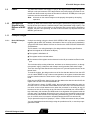
Figure 1-2. Reset, Minimum Design
AIA
CUSTOM DESIGN
ARESET\
CLKALWAYS
IRESET
The pod design must include a reset control logic. A minimum reset control logic design
is shown on Figure 1-2. This design ensures that the IRESET signal is at least 5 CPU
clocks.
1.4
Interrupt System
The ASIC ICE system supports up to 31 different interrupt sources. The pod needs to
have an interrupt controller, and pass the encoded interrupt vector through the pod interface. The core acknowledges the acceptance of an interrupt back to the pod.
Figure 1-3. Interrupt Encoding System
AIA
CUSTOM DESIGN
Register
Q0
IRQACKAD[4:0]
CLKIO
Priority
Encoder
IRQ0
IRQ1
IRQ(ENC)[4:0]
5
IRQACK
The AVR core uses a number of unencoded interrupt request input lines and responds
to an interrupt request on these by using the IRQACK and the IRQACKAD lines. The
ATasicICE Designer Guide
3
ATasicICE Designer Guide
IRQACK indicates that the interrupt with highest priority is going to be handled by the
core. The IRQACKAD lines reflects the interrupt vector address to the interrupt request
that is going to be handled. To reduce the number of lines between the ASIC ICE emulator and the pod, some of the core logic has to be duplicated in the pod design. Figure
1-3 shows how to implement the interrupt encoding system in a custom design.
When the priority encoded IRQ signals are set to zero, no interrupt will occur. If the
encoded IRQ[4:0] is nonzero, the value of IRQ[4:0] must be priority coded starting at 1
for highest priority and ending at 31 for lowest priority.
1.4.1
Interrupt Signals
IRQ[4:0] (I): The lines encode the currently highest priority interrupt source from the I/O.
IRQACK (O): When the core accepts an interrupt and starts handling it, it gives an
acknowledge signal on the IRQACK line. Based on this, the interrupt source can take
the necessary actions (e.g. clear interrupt request flag).
1.4.2
Extended Interrupt
Signals
GLOBINT (O): This line reflects the current value of the Global Interrupt flag in the Status Register.
IRQOK (O): Used during sleep to indicates to the sleep controller that an interrupt condition is established.
1.4.3
Custom Design
Without Interrupt
Support
If the interrupt system is not in use the pod must force all the interrupt request (IRQ4:0)
lines to a low level. This will ensure that no unwanted interrupts will occur.
1.5
Memory System
This section describes how the different memories are handled in the ASIC ICE.
1.5.1
Program Memory
Version 2 of the AVR Core handles up to 128K bytes (64K x 16-bit) of program memory.
This memory will always be handled inside the Emulator. There is no way of reading or
modifying this memory through the pod interface. Furthermore, there is no way of executing code in an external program memory. Due to handling the program memory internally, the user will have access to an unlimited number of code break points.
1.5.2
Data Memory
The Data memory area of an AVR consists of up to four areas. At the lowest addresses,
the Register file is mapped. Access to the registers will be handled internally in the core.
Next is the I/O area. Every access to the I/O area is reflected on the interface by the use
of the I/O read/write strobes (i.e. in the same way for load/store as for in/out.) except for
the I/O locations listed in the table below. Following the I/O area, there is an optional onchip data memory. If the ASIC has on board RAM, then this should be handled in the
Emulator. Last, the ASIC may have an external memory interface. If the ASIC has an
external memory, then this needs to be handled on the pod. The registers and the internal SRAM memory cannot be accessed from the pod.
The sizes of the register file and the I/O area are constant (32 registers, 64 I/O locations). The sizes of and the border between internal and external data memories can
change and needs to be configured by the user to ensure that the correct read and write
strobes are generated.
1.5.3
EEPROM Memory
If EEPROM memory is required in the ASIC, then this memory needs to be placed on
the pod together with the EEPROM interface. The EEPROM is, in the AVR standard
parts, accessed through I/O registers, and since the I/O registers are being handled in
the pod, the pod needs to take full responsibility of the EEPROM memory.
4
ATasicICE Designer Guide
ATasicICE Designer Guide
1.5.4
I/O Locations
Handled in the Core
The following addresses in the I/O space will be handled directly in the core:
Name
I/O Address
Data address
Comment
SREG
0x3F
0x5F
Status Register
SPH
0x3E
0x5E
Stack Pointer High
SPL
0x3D
0x5D
Stack Pointer Low
RAMPZ
0x3B
0x5B
Only if Program Memory > 64K Byte
If the emulator is configured to use more than 64K bytes program memory, then the core
will take control of I/O location 0x3B and use it for the ELPM instruction. Otherwise, this
I/O location can be used freely on the pod. No I/O read strobe will be generated when
the I/O locations handled by the core are read. The configuration is done from AVR Studio in the emulator options menu.
1.5.5
Memory Busses
ADR[15:0]: During RUN mode, ADR[15:0] are connected directly to the I/O and Memory
address bus of the Core. When the Emulator is stopped, the same lines are used by the
Emulator system to access resources on the pod and its surroundings.
DBUS[7:0]: During RUN mode, DBUS[7:0] are connected directly to the I/O and Memory
data bus of the Core. When the Emulator is stopped, the same lines are used to extract
information from the pod.
1.5.6
Memory Access
Control Signals
(From Emulator)
XRAMRE: XRAM Read Enable signal. During RUN mode, XRAMRE comes directly
from the Core. It can be configured through the software front end what address the
Core changes from accessing internal memory (on the Emulator) to accessing memory
on the pod.
XRAMWE: XRAM Write Enable signal. During RUN mode, XRAMWE comes directly
from the Core. It can be configured what address the Core changes from accessing
internal memory (on the Emulator) to accessing memory on the pod.
IORE: IO Read Enable signal. During RUN mode, IORE comes directly from the Core.
IOWE: IO Write Enable signal. During RUN mode, IOWE comes directly from the Core.
1.5.7
Wait State Control
Signals
MRAMACK: (Core output) Information supplied by the core to the pod to indicate that
the core will attempt to access RAM in two consecutive cycles (call and return instructions). This means that the pod might need to insert extra wait-states.
CPUWAIT: (Core input) This line is used to wait the processor. It must be used during
external memory accesses which cannot complete within the minimum time frame.
1.5.8
Data Bus Contention The AVR core data bus has no tri-state control at the interface to the I/O.
In the emulator, there is a tri-state control in the pads from the gate-array holding the
AVR core. The custom design should only drive this bus when either IORE or XRAMRE
is active. In all other cases, the core is driving the data bus. If the internal data bus in the
core has a valid signal, the value of this signal will be reflected at the data bus to the
POD. If the internal data bus in the core is hi-Z, the emulator is still driving the data bus
to the POD, but the value is indeterminate.
IMPORTANT!
■ The emulator exaggerates the risk for bus contention in the ASIC, in the sense that
the emulator AVR core drives the bus when the bus signal should not be trusted.
■
If the ASIC/FPGA on the POD uses the data bus for other purposes than core access,
the data bus must be isolated on the POD (or in the FPGA on the POD).
■
If an ASIC uses the core data bus under other circumstances than core access, this
function is still supported in the emulator.
ATasicICE Designer Guide
5
ATasicICE Designer Guide
■
The internal registers inside the AVR core are: Stack Pointer High, Stack Pointer Low,
Status Register and RAMPZ (if enabled). If the core reads these registers, the IORE
signal at the POD remains low. This simplifies the design of the tri-state control in the
POD FPGA. The IORE and XRAMRE signals can be used to qualify when the FPGA
should drive the data bus, without having to check that the address really is contained
within the FPGA.
■
When the emulator is in stop mode, the emulator reads out data from the POD FPGA
by using the IORE and IOWE strobe signals. No particular precautions needs to be
taken in the FPGA in order to support this function as long as the IORE strobe
controls the direction of the data bus from the POD.
1.6
Timing Issues
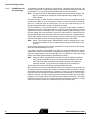
The ASIC ICE environment is different from a final ASIC. Use Figure 1-4 to calculate the
extra delay caused by the ASIC ICE. The delay values are absolute worst case values
(@70°C).
Figure 1-4. ASIC ICE, Timing Considerations
AVR ICEPRO ASIC
CUSTOM DESIGN
AVR CORE GATE ARRAY
D
Q
tint < 9ns
tPD< 1ns
Q
(Internal AIA
FPGA delay)
Q
tPAD
<
3ns
tlineCCK<2ns
<43ns
tPAD
<
*ns
Q
Q
tPAD<*ns
(Internal AIA
FPGA delay)
D
Q
tSETUP
D
tlineCCK<4ns
tint < 9ns
tPAD
<
3ns
tPAD
<
5ns
tlineCCK<4ns
tlineCCK<2ns
<26ns
tlineCCK<2ns
CLOCK GEN
(Low Skew)
tlineCCK<4ns
tPAD
<
*ns
tPAD
<
*ns
1.7
Sleep Control
SLEEPI: When the core performs a SLEEP instruction, this is reflected on this line. If the
ASIC needs a Sleep system, then this signal needs to be handled on the pod.
1.8
Watchdog
System
If the ASIC needs a Watchdog system, the pod should handle this. The WDRI line indicates that the core performs a WDR instruction. This signal can directly be used to reset
a watchdog timer. A watchdog timer overflow can force a internal reset using the IRESET signal, if the watchdog is enabled.
Note: The IRESET should be held high for at least 5 core clocks (CLKIO) to ensure
that the core is reset.
1.8.1
Watchdog Control
Signals
WDRI: When the core performs a WDR instruction, this is reflected on this line.
6
ATasicICE Designer Guide
ATasicICE Designer Guide
1.9
Power
The ASIC ICE emulator can supply 1A (5V) to the target (custom design) through the
VDD pin on the pod connector. If the target has its own power supply, this must be connected and disconnected only when the emulator is turned off. All GND pins on the pod
connector must be connected to ground.
Note: All circuits on the custom design must be properly decouped by decoupling
capacitors.
1.10
Unsupported
Signals in this
Release of ASIC
ICE
IOBUSY (I): When the Emulator stops, there might be operations in progress in some of
the I/O devices (for instance a character which is being transmitted using a UART). The
IOBUSY line is used to signal back to the Emulator that even though the Emulator is
stopped, the pod is still operating, and that it cannot answer any requests before the
IOBUSY goes inactive.
1.11
Example Designs
1.11.1
Basic I/O Example
Design
A simple test design using the Atmel ASIC ICEPRO POD is provided on a diskette
together with the ASIC ICE emulator. Information of how to use the pod is described in
ATasicICE POD User’s Manual. All files are found on the AVR ATasicICE AUXILIARY
FILES diskette.
The file xtestio.v is a verilog description of a design with the following specifications:
■ One 8-bit register at I/O location 0x1B (hex).
■
The register is initialized to 0.
■
The register can be read and written.
■
The contents of the register can be observed on the I/O pins marked as PortA on the
pod.
The clocks should be running all the time, and there are no interrupt services, so the signals cpuwait, irq[4:0], clkstopcore and clkstopio are all grounded, while clken is high.
There is a reset logic that stretches the reset pulse to 5 cycles and synchronizes it to the
internal clock.
To reset the register, the design makes use of the fact that the data bus from the AVR
core is 0 when IRESET is high. Under normal operation, the register is loaded with data
from the data bus when the iowe strobe is high, and the address bus has the value
0x1B.
Each time the IORE strobe signal is high and the address bus has the value 0x1B, the
register value is sent out to the internal data bus.
The PAD control is simply: If IORE is high, then send the internal data bus value out
from the FPGA. If not, send the external data bus into the FPGA. This means that there
is a value on the internal data bus even when the processor is not writing to any I/O
locations, but this is OK as long as the I/O does not use the data bus unless IORE is
high. Note that in this emulator, the IORE strobe is not high when I/O registers inside the
core are read. The designer will therefore never run into bus contention because both
the internal I/O and the POD I/O are responding simultaneously, (this is an emulator feature, in an ASIC, there is no need to use pads between the AVR core and the I/O.)
The pin placement script for a Synopsys™ / Xilinx™ FPGA environment is also provided.
You can download and test this design using the provided mcs-file, or use the pre-programmed FLASH.
ATasicICE Designer Guide
7
ATasicICE Designer Guide
1.11.2
8
AT90MEGA103 I/O
Example Design
The diskette includes an example of a large design: The Atmel ATmega103 I/O. The
complete Verilog code is not provided because it is an intellectual property of Atmel, and
not distributed. You can still download the FPGA and test it on the emulator.
Note: You will not be able to understand the design from this top-level description, but
the file is included as an example on how to implement large designs on the
ASIC emulator.
The basic concept for ASIC emulation is that the HDL-code from the ASIC should be
reused in the FPGA as much as possible in order to emulate the ASIC functionally.
Since it is 2 different types of technologies, you can never trust the timing, so we
strongly recommend that the design is a synchronous design.
The file x01838io.v is the top-level Verilog™ description of this design. x01838io.v
instantiates iomodule , wdog and sleepcnt. iomodule could be the same I/O verilog
description as used in the standard chip. The sleep controller (sleepcnt) makes use of
the clock gating logic in the emulator to control the sleep functions. A watch dog timer
(wdog) stretches the ireset signal and resets the circuit if it times out. It might be necessary to make special versions of such modules in order to make use of the clock gating
functions in the ASIC emulator and simplify asynchronous logic in the FPGA.
Note: Under "//The interrupt system. IRQACKADR is made by delaying irqack", there
is a complete example on how to implement the interrupt priority encoder to the
avrcore.
Note that both xramre and iore must be considered for the pad control of this design,
since the external RAM space is in use.
If you want to test the on-board RAM on the POD, you must strap between the signals
xrepisdel and xrepnodel, and between xwepisdel and xwepnodel. This is a trick used to
delay the strobe signals to the external RAM, since it is difficult to control the timing
exactly in an FPGA (without designing specifically for FPGAs).
Note: Under the label "// Asynchronous timer stuff" there is an example on how the
clock signals should NOT be used. The extra multiplexer between clkio and
cktim makes the clock skew between the AVR core and the I/O larger and
should be avoided. Try to use the clock gating logic in the emulator only.
The pin placement script for this design is also provided on the disk.
Often, the there is a need to have different functions in a module when the AVR core
accesses the module and when the emulator is stopped, and the user wants to access
the module via the front end software. For instance, in a timer, you do not want the timer
to advance when the emulator is stopped and the user accesses the I/O. The file tim0.v
shows an example. The same verilog description is used in the ASIC and in the ASIC
emulator, but a compiler switch "EM" selects between these two situations. The signal
CLKRUN (called runmod in this module) determines whether the emulator is in stop
mode or not, and the counter is not advanced as long as runmod is high.
ATasicICE Designer Guide
ATasicICE Designer Guide
1.12
Appendix A:
Pod Connector
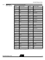
Direction as seen from the Emulator.
Pin(Dir)
Connector Name
Pin(Dir)
Connector Name
1 (O)
GND
33 (I/O)
DBUS6
2 (O)
GND
34 (O)
IOWE
3 (O)
ADR0
35 (I/O)
DBUS7
4 (O)
VDD
36 (O)
MRAMACK
5 (O)
ADR1
37 (O)
IOEXTEND0
6 (O)
ADR8
38 (I)
IOBUSY
7 (O)
ADR2
39
NC(*)
8 (O)
ADR9
40 (O)
IOEXTEND1
9 (O)
ADR3
41 (O)
GND
10 (O)
ADR10
42 (O)
IOEXTEND2
11 (O)
ADR4
43 (O)
CLKALWAYS
12 (O)
ADR11
44 (I)
EXTCLKIN
13 (O)
ADR5
45 (O)
EXTCLKEN
14 (O)
ADR12
46 (O)
CLKRUN
15 (O)
ADR6
47 (O)
CLKOSC
16 (O)
ADR13
48 (O)
CLKIO
17 (O)
ADR7
49 (I)
CLKSTOPIO
18 (O)
ADR14
50 (I)
CLKSTOPCORE
19 (O)
ARESET
51 (I)
CPUWAIT
20 (O)
ADR15
52 (O)
IOEXTEND3
21 (I/O)
DBUS0
53 (O)
IOEXTEND4
22 (O)
SLEEPI
54 (I)
23 (I/O)
DBUS1
55 (I)
IRQ0
24 (O)
WDRI
56 (I)
IRQ1
25 (I/O)
DBUS2
57 (I)
IRQ2
26 (I)
IRESET
58 (I)
IRQ3
27 (I/O)
DBUS3
59 (I)
IRQ4
28 (O)
XRAMRE
60 (O)
IRQACK
29 (I/O)
DBUS4
61 (O)
GLOBINT
30 (O)
XRAMWE
62 (O)
IRQOK
31 (I/O)
DBUS5
63 (O)
GND
32 (O)
IORE
64 (O)
GND
(*) Do not connect this pin to any power or I/O.
ATasicICE Designer Guide
9
AVR ATasicICE Designer Guide
1.13
Appendix B:
Basic I/O
Example Design
Verilog Files
xtestio.v
//****************************************************************
// Module: xtestio
//
//
// Time of last save:
$Date: 1998/02/17 08:25:27 $
// Revision:
$Revision: 1.1 $
//
// Function:
//
Short example of how to connect a simple I/O module to the ASIC
//
ICEPRO.
//
A register at I/O address 0x1B can be written and read. The content
//
of this register is set on the output pins marked PORTA on the
//
ATMEL ASIC ICEPRO pod.
//
//*****************************************************************
module xtestio (
ireset, cpuwait,
irq4,irq3,irq2,irq1,irq0,
dbus7, dbus6, dbus5, dbus4, dbus3, dbus2, dbus1, dbus0,
adr5, adr4, adr3, adr2, adr1, adr0,
areset_b,
iore, iowe,
clkio, clken,
clkstopcore,clkstopio,
fio7, fio6, fio5, fio4, fio3, fio2, fio1, fio0 );
output ireset;// Synchronous reset (active high)
output cpuwait;// HALT AVR core
output
output
output
output
output
irq4;// Interrupts
irq3;
irq2;
irq1;
irq0;
inout
inout
inout
inout
inout
inout
inout
inout
dbus7;// data bus
dbus6;
dbus5;
dbus4;
dbus3;
dbus2;
dbus1;
dbus0;
input
input
input
input
input
input
adr5;// The I/O address bus.
adr4;
adr3;
adr2;
adr1;
adr0;
input
input
input
input
output
output
output
areset_b;// Asynchronous reset (active low)
iore;// Read strobe
iowe;// Write strobe
clkio;// ckio from clock FPGA
clken;// Clock enable signal
clkstopcore;// Stop core clock
clkstopio;// Stop I/O clock
output fio7;// Output port.
output fio6;
output fio5;
10
ATasicICE Designer Guide
output
output
output
output
output
fio4;
fio3;
fio2;
fio1;
fio0;
// Declarations
reg [5:0] sync_reset;
reg [7:0]port_register;
wire [7:0] dbus;
wire [5:0] ioadr;
wire port_reg_addr;
// Unused output signals to the AVR core or emulator
assign cpuwait = 1'b0;
assign {irq4,irq3,irq2,irq1,irq0} = 5'b0;
assign clken = 1'b1;
assign clkstopcore = 1'b0;
assign clkstopio = 1'b0;
// Synchronize the asynchronous reset signal. Stretch reset signal to 5
pulses.
always @(posedge clkio)
sync_reset = {sync_reset[4:0], ~areset_b};
assign ireset = |(sync_reset[5:1]);
// Pad control
assign ioadr = {adr5, adr4, adr3, adr2, adr1, adr0};
assign {dbus7,dbus6,dbus5,dbus4,dbus3,dbus2,dbus1,dbus0} = (iore) ? dbus :
8'bz;
assign dbus = (~iore) ? {dbus7,dbus6,dbus5,dbus4,dbus3,dbus2,dbus1,dbus0}
:8'bz;
assign {fio7,fio6,fio5,fio4,fio3,fio2,fio1,fio0} = port_register;
// Main function of the module
assign port_reg_addr = (ioadr == 6'h 1b);
assign dbus = ~(port_reg_addr & iore) ? 8'bz : port_register;
always @(posedge clkio)
if (ireset | port_reg_addr & iowe)
port_register = dbus;
endmodule
ATasicICE Designer Guide
11
ATasicICE Designer Guide
set_pin_placement.scr
set_attribute{clkio}
set_attribute{clken}
"pad_location"-typestring"P118"
"pad_location"-typestring"P44"
set_attribute{clkstopcore} "pad_location"-typestring"P33"
12
set_attribute{clkstopio}
"pad_location"-typestring"P32"
set_attribute{ireset}
"pad_location"-typestring"P20"
set_attribute{areset_b}
"pad_location"-typestring"P15"
set_attribute{cpuwait}
"pad_location"-typestring"P34"
set_attribute{irq4}
"pad_location"-typestring"P50"
set_attribute{irq3}
"pad_location"-typestring"P49"
set_attribute{irq2}
"pad_location"-typestring"P48"
set_attribute{irq1}
"pad_location"-typestring"P47"
set_attribute{irq0}
"pad_location"-typestring"P46"
set_attribute{dbus0}
"pad_location"-typestring"P4"
set_attribute{dbus1}
"pad_location"-typestring"P5"
set_attribute{dbus2}
"pad_location"-typestring"P8"
set_attribute{dbus3}
"pad_location"-typestring"P9"
set_attribute{dbus4}
"pad_location"-typestring"P10"
set_attribute{dbus5}
"pad_location"-typestring"P11"
set_attribute{dbus6}
"pad_location"-typestring"P12"
set_attribute{dbus7}
"pad_location"-typestring"P13"
set_attribute{adr5}
"pad_location"-typestring"P230"
set_attribute{adr4}
"pad_location"-typestring"P228"
set_attribute{adr3}
"pad_location"-typestring"P225"
set_attribute{adr2}
"pad_location"-typestring"P223"
set_attribute{adr1}
"pad_location"-typestring"P217"
set_attribute{adr0}
"pad_location"-typestring"P215"
set_attribute{iore}
"pad_location"-typestring"P25"
set_attribute{iowe}
"pad_location"-typestring"P26"
set_attribute{fio0}
"pad_location"-typestring"P176"
set_attribute{fio1}
"pad_location"-typestring"P175"
set_attribute{fio2}
"pad_location"-typestring"P172"
set_attribute{fio3}
"pad_location"-typestring"P171"
set_attribute{fio4}
"pad_location"-typestring"P170"
set_attribute{fio5}
"pad_location"-typestring"P169"
set_attribute{fio6}
"pad_location"-typestring"P168"
set_attribute{fio7}
"pad_location"-typestring"P167"
ATasicICE Designer Guide