1
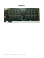
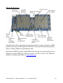
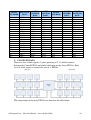
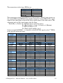
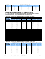
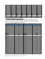
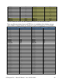
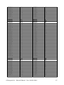
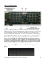
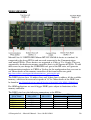
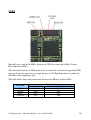
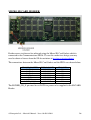
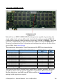
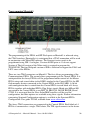
Merrick3 User Manual
Issue – 1.0
© Enterpoint Ltd. – Merrick3 Manual – Issue 1.0 02/11/2011
11
Kit Contents
You should receive the following items with your Merrick3 development kit:
1 - Merrick3 Board
2 - Programming Cable
Foreword
PLEASE READ THIS ENTIRE MANUAL BEFORE PLUGGING IN
OR POWERING UP YOUR MERRICK3 BOARD.
PLEASE TAKE SPECIAL NOTE OF THE WARNINGS WITHIN
THIS MANUAL.
Trademarks
Spartan-6, ISE, Webpack, EDK, COREGEN, Xilinx are the registered trademarks of Xilinx Inc,
San Jose, California, US.
Merrick3 is a trademark of Enterpoint Ltd.
© Enterpoint Ltd. – Merrick3 Manual – Issue 1.0 02/11/2011
22
Contents
Kit Contents
Foreword
Trademarks
MERRICK3 BOARD
INTRODUCTION
MERRICK3 FEATURES
FPGAs
CONNECTIONS BETWEEN FPGAS
1. Between Communications FPGA and Control FPGA
2. Between Control FPGA and Array FPGAs
1 Patch bus signals
2. Clock Signals
3. Configuration signals
4. Individual FPGA Patch Signals
3. Between Communications FPGA and Array FPGAs
4. Between Adjacent Array FPGAs
5. Between the Control FPGA and the Expansion connector
DEVICE ID CODES
SPI FLASH
DDR3 MEMORY
LEDS
PCIE INTERFACE
BATTERY
MICRO SD CARD HOLDER
CLOCK GENERATOR
INPUT POWER CONNECTIONS
HEAT SINKS
POWER REGULATORS
PROGRAMMING MERRICK3
MECHANICAL
Medical and Safety Critical Use
Warranty
Support
© Enterpoint Ltd. – Merrick3 Manual – Issue 1.0 02/11/2011
2
2
2
4
5
6
7
8
8
8
8
9
10
12
14
15
18
20
21
23
24
27
27
28
29
30
30
31
32
35
36
36
36
33
MERRICK3
© Enterpoint Ltd. – Merrick3 Manual – Issue 1.0 02/11/2011
44
Introduction
Welcome to your Merrick3 board. Merrick3 is a Spartan-6 based FPGA development
board offering a highly powerful approach to prototyping FPGA and System designs.
Merrick3 is a product for the high performance computing (HPC) marketplace.
Based on an array of 24 XC6SLX150 FPGAs and 16 DDR3 this board delivers
algorithm processing up to 10000X that of a X86 processor whilst operating with a
power envelope of between 10-200W. In addition the board features high speed
routing across the array and array reload (under 0.25 seconds), a board stacking
interface and a PCI-E interface. We are also able to provide a separate algorithm
implementation service for customers.
Merrick3 also offers a highly powerful approach to prototyping FPGA and System
designs.
The aim of this manual is to assist in using the main features of Merrick3.
There are features that are beyond the scope of the manual. Should you need to use
these features then please email [email protected] for detailed instructions.
Merrick3 is currently fitted with XC6SLX150-2FGG484C Spartan-6 devices. Other
variants may be offered at a later date or as an OEM product. Please contact us on
[email protected] should you need further information.
© Enterpoint Ltd. – Merrick3 Manual – Issue 1.0 02/11/2011
55
Merrick3 Features
FPGA Left
Array Bank
Memory
Card
Holder
2 GBit ddr3
serving
communica
tions FPGA
2x128Mb
SPI Flash
memory
Clock Generator
Expansion/stacking
interface
PCIE
Control FPGA
Interface
XC6SLX150T
Communications
FPGA
XC6SLX45T
12
xc6slx150csg484
devices per bank
2 GBit ddr3
serving control
FPGA
FPGA Right
Array Bank
8x2 GBit
DDR3 per
FPGA bank
Your Merrick3 will be supplied un-programmed. Unless you have bought an OEM
product your board will be supplied with either a Prog2 parallel port programming
cable or a Prog3 USB port programming cable.
The Spartan-6 FPGAs on the standard Merrick3 board are not supported by the free
Webpack version of ISE. You will need version 11.1 SP4, or later, of the ISE tools,
which are available from Xilinx at www.xilinx.com.
© Enterpoint Ltd. – Merrick3 Manual – Issue 1.0 02/11/2011
66
FPGAs
Top Row
Centre
Row
Bottom
Row
Communications
FPGA
12 Left Array
FPGAs
Control
FPGA
12 Right Array
FPGAs
Merrick3 has a total of 26 FPGAs. There are 24 array FPGAs, one Control FPGA and
one Communications FPGA. The standard arrangement is:
Communications FPGA – XC6SLX45T-FGG484C
Control FPGA – XC6SLX150T-FGG900C
Array FPGAs - XC6SLX150-CSG484C
Merrick3 is normally available with commercial grade -2 speed devices fitted in the
XC6SLX150 size. Should you have an application that needs different size FPGAs,
industrial specification parts or faster speed grades please contact us for a quote at
[email protected].
The Merrick3 FPGAs are highly interconnected. The diagram below shows the major
sets of interconnections:
Fig1 Merrick major interconnections
© Enterpoint Ltd. – Merrick3 Manual – Issue 1.0 02/11/2011
77
CONNECTIONS BETWEEN FPGAs
1. Between Communications FPGA and Control FPGA
There are 20 connections between the Communications FPGA and the Control
FPGA, arranged as 10 pairs between 3.3V IOs. The table below shows the pin
connections:
SIGNAL NAME
COMMS_BUS1
COMMS_BUS2
COMMS_BUS3
COMMS_BUS4
COMMS_BUS5
COMMS_BUS6
COMMS_BUS7
COMMS_BUS8
COMMS_BUS9
COMMS_BUS10
COMMS_BUS11
COMMS_BUS12
COMMS_BUS13
COMMS_BUS14
COMMS_BUS15
COMMS_BUS16
COMMS_BUS17
COMMS_BUS18
COMMS_BUS19
COMMS_BUS20
COMMUNICATIONS FPGA
J3
J1
F3
E4
D2
D1
G3
G1
J4
H3
H2
H1
C1
B1
H4
G4
K2
K1
E3
E1
CONTROL FPGA
V26
V27
R21
R22
R24
R25
T28
T30
U27
U28
U29
U30
R27
R28
T26
T27
Y24
Y25
T24
T25
2. Between Control FPGA and Array FPGAs
There are a total of 4 sets of connections between the control FPGA and the array
FPGAs.
1. PATCH BUS SIGNALS
There are 120 connections shown in the diagram above (fig1) arranged as 20
signals (10 pairs) each to the nearest FPGA in each row. The connections are
shown in the table below. In the schematics and .ucf file these connections are
called, for example, PATCH_LH1BUS(1 to 20) for the 20 signals connected to
the 20 RBUS signals on the top left row FPGA nearest to the Control FPGA
and PATCH_RH3BUS(1 to 20) for the 20 signals. connected to the 20 LBUS
signals on the bottom right row FPGA nearest to the Control FPGA. These
connections are between IOs operating at 3.3V.
© Enterpoint Ltd. – Merrick3 Manual – Issue 1.0 02/11/2011
88
SIGNAL
NUMBER
LEFT TOP
ROW
1
2
3
4
5
6
7
8
9
10
11
12
13
14
15
16
17
18
19
20
AB10
AB9
AC11
AD11
AA11
AB11
AE13
AF13
AC15
AD15
AD14
AE14
Y15
AA15
AB17
AD17
AB13
AC13
AE17
AF17
LEFT
CENTRE
ROW
AD12
AE12
AB14
AC14
AJ15
AK15
Y16
AB16
AJ17
AK17
AH16
AK16
AD18
AE18
AA18
AB18
AF16
AG16
W20
Y20
LEFT
BOTTOM
ROW
AA19
AB19
AC19
AD19
AD20
AE20
AB21
AC21
AE23
AF23
AA22
AC22
AE24
AF24
AF25
AG25
AD22
AE22
AD24
AC24
RIGHT
TOP ROW
D6
C6
E7
D7
F8
E8
K10
J10
L12
K12
H11
G11
M13
L13
J13
H13
J12
H12
L14
K14
RIGHT
CENTRE
ROW
G14
F14
F15
E15
B15
A15
H17
G17
C16
A16
E16
D16
B17
A17
G18
F18
H16
G16
L17
K17
RIGHT
BOTTOM
ROW
G20
F20
K20
J20
L21
K21
G22
F22
J22
H22
F24
E24
D24
C24
B25
A25
F23
E23
E25
D25
2. CLOCK SIGNALS
There are also 4 clock signals (2 pairs operating at 3.3v) which connect
between the Control FPGA and global clock pins on the Array FPGAs. Each
set of 4 clock signals is routed to a row of 4 FPGAs.
The connections to the array FPGAs are shown in the table below:
© Enterpoint Ltd. – Merrick3 Manual – Issue 1.0 02/11/2011
99
SIGNAL NAME
ARRAY FPGA PIN
CLK1
CLK2
CLK3
CLK4
B10
A10
C11
A11
The connections to the Control FPGA are shown in the table below. In the
schematics and .ucf file these connections are called, for example,
CLOCKS_LH1_(1 TO 4) for the 4 signals connected to the CLK(1 TO 4)
signals on the four top left row FPGAS and CLOCK_RH3_(1 to 4) for the 4
signals connected to the CLK(1 TO 4) signals on the four bottom right row
FPGAS.
ARRAY
SIGNAL
NAME
CLK1
CLK2
CLK3
CLK4
LEFT TOP
ROW
AC3
AC1
AB4
AB3
LEFT
CENTRE
ROW
AD7
AE7
AB7
AB6
LEFT
BOTTOM
ROW
AC28
AC27
AE25
AE26
RIGHT
TOP ROW
N5
N4
J5
J4
RIGHT
CENTRE
ROW
T9
T8
P7
P6
RIGHT
BOTTOM
ROW
N27
N28
N29
N30
3. CONFIGURATION SIGNALS
There are 23 configuration signals routed along each block of 4 FPGAs, with
an individual Chip Select signal to each FPGA. This is to enable the Control
FPGA to initiate reconfiguration of the array FPGAs. A 16 bit configuration
data bus plus CCLK, PROGRAM_B, INIT_B, DONE and RDWR_B signals
are connected to the Control FPGA as shown in the diagram below.
© Enterpoint Ltd. – Merrick3 Manual – Issue 1.0 02/11/2011
10
1
The connections to the Array FPGAs are shown in the table below:
SIGNAL NAME
CONFIG_DATA0
CONFIG_DATA1
CONFIG_DATA2
CONFIG_DATA3
CONFIG_DATA4
CONFIG_DATA5
CONFIG_DATA6
CONFIG_DATA7
CONFIG_DATA8
CONFIG_DATA9
CONFIG_DATA10
CONFIG_DATA11
CONFIG_DATA12
CONFIG_DATA13
CONFIG_DATA14
CONFIG_DATA15
CONFIG_DATA16
CONFIG_DATA17
CONFIG_DATA18
CONFIG_DATA19
CONFIG_DATA20
CONFIG_DATA21
CONFIG_DATA22
ARRAY
FPGA PIN
Y17
V13
W13
AA8
AB8
W6
Y6
Y9
AA6
AB6
V15
W15
Y16
AA12
Y11
AB11
AA1
Y5
U16
W17
AB9
Y18
U15
SIGNAL FUNCTION
16 BIT CONFIGURATION DATA BIT 0
16 BIT CONFIGURATION DATA BIT 1
16 BIT CONFIGURATION DATA BIT 2
16 BIT CONFIGURATION DATA BIT 3
16 BIT CONFIGURATION DATA BIT 4
16 BIT CONFIGURATION DATA BIT 5
16 BIT CONFIGURATION DATA BIT 6
16 BIT CONFIGURATION DATA BIT 7
16 BIT CONFIGURATION DATA BIT 8
16 BIT CONFIGURATION DATA BIT 9
16 BIT CONFIGURATION DATA BIT 10
16 BIT CONFIGURATION DATA BIT 11
16 BIT CONFIGURATION DATA BIT 12
16 BIT CONFIGURATION DATA BIT 13
16 BIT CONFIGURATION DATA BIT 14
16 BIT CONFIGURATION DATA BIT 15
PROG_B
INIT_B
DONE
CCLK
RDWR_B
M0
M1
The connections to the Control FPGA are shown below:
CONFIG_
DATA
SIGNAL
0
1
2
3
4
5
6
7
8
9
10
11
12
13
14
15
LEFT TOP
ROW
N3
AA5
R1
T2
T3
T1
U1
AD3
T6
T4
R3
AA4
P1
R4
R6
R5
LEFT
CENTRE
ROW
AK3
AG5
AE5
Y8
AA10
Y9
W11
AA9
W10
Y11
AJ4
AK5
AH5
AF6
AD6
AE6
LEFT
BOTTOM
ROW
AG27
AJ29
AJ30
AE30
AE28
AE29
AA29
AC29
AA28
AA27
AH30
AK29
AJ28
AF28
AD26
AF30
© Enterpoint Ltd. – Merrick3 Manual – Issue 1.0 02/11/2011
RIGHT
TOP ROW
N1
L1
K4
H2
H3
H1
G4
J1
G1
G5
L4
L3
M1
K3
K2
K1
RIGHT
CENTRE
ROW
E1
B2
D2
A5
C4
B5
C5
D4
E5
M7
M6
A2
C1
A3
D3
B3
RIGHT
BOTTOM
ROW
P22
R30
U24
W28
V28
W30
W27
P27
Y28
P5
P28
R29
P24
U25
V24
V23
11
1
16
17
18
19
20
V7
U3
P2
P3
R7
V9
V10
AH3
Y3
AC6
AA24
AA25
AK27
AH27
AE27
F1
G3
M2
M3
H4
H6
D5
D1
E4
A4
Y26
Y30
P30
P23
V30
The M0 and M1 signals for the left side array and right side array are routed
independently. The table below shows the connections to the Control FPGA:
SIGNAL
M0
M1
LEFT ARRAY PIN
W22
Y23
RIGHT ARRAY PIN
W21
Y22
The individual Chip select pins, which connect to pin AB5 of each array FPGA
(CSO_B) are connected to the Control FPGA as follows, FPGA1 being nearest to
the control FPGA and FPGA4 being furthest from the Control FPGA:
LEFT TOP ROW
LEFT CENTRE ROW
LEFT BOTTOM ROW
RIGHT TOP ROW
RIGHT CENTRE ROW
RIGHT BOTTOM ROW
FPGA1
W3
AG29
AD28
F4
N9
Y27
FPGA2
W1
W9
AD27
F2
N10
AB28
FPGA3
V8
AH24
AD30
L6
N8
AB30
FPGA4
U4
AG28
AA30
F3
J6
AC30
4. INDIVIDUAL FPGA PATCH SIGNALS
Lastly there are 4 signals (2 pairs operating at 3.3V) which are routed to each
individual FPGA from the Control FPGA.
© Enterpoint Ltd. – Merrick3 Manual – Issue 1.0 02/11/2011
12
1
The connections to the Array FPGAs are:
SIGNAL NAME
PATCH1
PATCH2
PATCH3
PATCH4
ARRAY FPGAS
D17
C16
B18
A18
The connections to the Control FPGA are shown below, FPGA1 being nearest to
the control FPGA and FPGA4 being furthest from the Control FPGA. The signal
names in the table below relate to the Array signal names in the table above. The
schematic and .ucf file signal names take the form:
PatchAB_C_D where A = R(Right Array) or L(Left Array)
B = Row number = 1(top), 2(Centre) or 3(Bottom)
C= FPGA number 1 to 4
D = Patch signal number 1 to 4
So for example PATCHL1_3_4 connects to the PATCH4 signal on the 3rd FPGA
in the top row of the left array.
SIGNAL
NAME
PATCH1
PATCH2
PATCH3
PATCH4
SIGNAL
NAME
PATCH1
PATCH2
PATCH3
PATCH4
SIGNAL
NAME
PATCH1
PATCH2
PATCH3
PATCH4
SIGNAL
NAME
PATCH1
PATCH2
PATCH3
PATCH4
SIGNAL
NAME
PATCH1
PATCH2
PATCH3
PATCH4
FPGA1
AH7
AK7
AD8
AE8
FPGA1
AB12
AC12
AC9
AD9
FPGA1
AE19
AF19
M20
L20
FPGA1
F9
E9
D8
C8
FPGA1
M15
K15
L11
K11
LEFT TOP ROW
FPGA2
FPGA3
AG8
AE11
AH8
AF11
AF7
AE9
AG7
AF9
LEFT CENTRE ROW
FPGA2
FPGA3
W14
Y14
Y13
AA14
W12
Y17
Y12
AA17
LEFT BOTTOM ROW
FPGA2
FPGA3
AB20
W19
AC20
Y19
AE21
AB23
AF21
AC23
RIGHT TOP ROW
FPGA2
FPGA3
B6
M10
A6
L10
B7
J8
A7
H8
RIGHT CENTRE ROW
FPGA2
FPGA3
H15
F13
G15
E13
J14
G12
H14
F12
© Enterpoint Ltd. – Merrick3 Manual – Issue 1.0 02/11/2011
FPGA4
AG6
AH6
AD10
AE10
FPGA4
AC16
AD16
AE15
AF15
FPGA4
M18
L18
Y21
AA21
FPGA4
H7
G7
F6
E6
FPGA4
F11
E11
G10
F10
13
1
SIGNAL
NAME
PATCH1
PATCH2
PATCH3
PATCH4
FPGA1
F21
E21
K19
J19
RIGHT BOTTOM ROW
FPGA2
FPGA3
F19
J18
E19
H18
H21
M19
G21
L19
FPGA4
F17
E17
H19
G19
3 Between Communications FPGA and Array FPGAs
Fig 1 above shows the 20 connections between the communications FPGA and
each row of 4 FPGAs. These interconnections are shown below.
Connections between the Communications FPGA and the Left Array:
SIGNAL
NUMBER
1
2
3
4
5
6
7
8
9
10
11
12
13
14
15
16
17
18
19
20
LEFT TOP ROW
COMMS
ARRAY
FPGA PIN FPGA PIN
W17
C17
Y18
A17
AA18
B16
AB18
A16
Y17
C15
AB17
A15
V17
B14
W18
A14
AA14
H11
AB14
G11
U16
B12
V15
A12
V13
D10
W13
C10
U14
D9
U13
D8
Y16
C13
W15
A13
AA2
C7
AA1
A7
LEFT CENTRE ROW
COMMS
ARRAY
FPGA PIN FPGA PIN
AA16
C17
AB16
A17
Y15
B16
AB15
A16
W14
C15
Y14
A15
Y13
B14
AB13
A14
T15
H11
U15
G11
W12
B12
Y12
A12
Y11
D10
AB11
C10
V11
D9
W11
D8
AA12
C13
AB12
A13
T12
C7
U12
A7
LEFT BOTTOM ROW
COMMS
ARRAY
FPGA PIN FPGA PIN
W10
C17
Y10
A17
AA10
B16
AB10
A16
Y9
C15
AB9
A15
W9
B14
Y8
A14
AA6
H11
AB6
G11
Y7
B12
AB7
A12
Y5
D10
AB5
C10
AA4
D9
AB4
D8
AA8
C13
AB8
A13
W6
C7
Y6
A7
Connections between the Communications FPGA and the Right Array:
SIGNAL
NUMBER
1
2
3
4
5
6
7
8
RIGHT TOP ROW
COMMS
ARRAY
FPGA PIN FPGA PIN
B3
AB18
A3
AA18
B2
AA16
A2
AB16
F2
Y15
F1
AB15
R11
AA14
T11
AB14
RIGHT CENTRE ROW RIGHT BOTTOM ROW
COMMS ARRAY
COMMS
ARRAY
FPGA PIN FPGA PIN FPGA PIN FPGA PIN
D18
AB18
H13
AB18
D19
AA18
G13
AA18
B20
AA16
H12
AA16
A20
AB16
G11
AB16
C19
Y15
H10
Y15
A19
AB15
H11
AB15
B18
AA14
G9
AA14
A18
AB14
F10
AB14
© Enterpoint Ltd. – Merrick3 Manual – Issue 1.0 02/11/2011
14
1
9
10
11
12
13
14
15
16
17
18
19
20
T8
U8
R9
R8
T7
U6
U9
V9
T10
U10
V7
W8
W14
Y14
W12
Y12
W11
Y10
AA10
AB10
Y13
AB13
W9
Y8
G16
F17
D17
C18
E16
F16
F14
F15
C17
A17
H14
G15
W14
Y14
W12
Y12
W11
Y10
AA10
AB10
Y13
AB13
W9
Y8
E5
E6
F7
F8
C5
A5
D4
D5
G8
F9
C4
A4
W14
Y14
W12
Y12
W11
Y10
AA10
AB10
Y13
AB13
W9
Y8
4 Between Adjacent Array FPGAs
Each FPGA connects to its neighbours above, below and to each side (except
where a device connects to DDR3 instead). There are 38 connections from each
FPGA to its right/left neighbour (20 if LX45/LX75 devices are fitted) which are
connected as pairs of signals on 3.3V IO banks.
LEFT
SIGNAL NAME
LBUS1
LBUS2
LBUS3
LBUS4
LBUS5
LBUS6
LBUS7
LBUS8
LBUS9
LBUS10
LBUS11
LBUS12
LBUS13
LBUS14
LBUS15
LBUS16
LBUS17
LBUS18
LBUS19
LBUS20
LBUS21
LBUS22
LBUS23
LBUS24
LBUS25
LBUS26
LBUS27
LBUS28
PIN
C17
A17
B16
A16
C15
A15
B14
A14
H11
G11
B12
A12
D10
C10
D9
D8
C13
A13
C7
A7
F10
E10
D15
C14
C5
A5
C9
A9
RIGHT
SIGNAL NAME
RBUS1
RBUS2
RBUS3
RBUS4
RBUS5
RBUS6
RBUS7
RBUS8
RBUS9
RBUS10
RBUS11
RBUS12
RBUS13
RBUS14
RBUS15
RBUS16
RBUS17
RBUS18
RBUS19
RBUS20
RBUS21
RBUS22
RBUS23
RBUS24
RBUS25
RBUS26
RBUS27
RBUS28
© Enterpoint Ltd. – Merrick3 Manual – Issue 1.0 02/11/2011
PIN
AB18
AA18
AA16
AB16
Y15
AB15
AA14
AB14
W14
Y14
W12
Y12
W11
Y10
AA10
AB10
Y13
AB13
W9
Y8
R13
U13
T14
U14
Y7
AB7
T12
U12
15
1
LBUS29
LBUS30
LBUS31
LBUS32
LBUS33
LBUS34
LBUS35
LBUS36
LBUS37
LBUS38
B6
A6
D7
C8
B8
A8
D6
C6
D13
D12
RBUS29
RBUS30
RBUS31
RBUS32
RBUS33
RBUS34
RBUS35
RBUS36
RBUS37
RBUS38
T10
U10
U9
V9
V11
W10
V7
W8
R11
T11
Signals shown in yellow are not connected on LX75 or LX45 FPGA sizes
There are 80 connections from each FPGA to its neighbour above/below (except
where DDR3 is fitted) which are connected as pairs of signals on 1.5V IO banks.
UP
SIGNAL NAME
UBUS1
UBUS2
UBUS3
UBUS4
UBUS5
UBUS6
UBUS7
UBUS8
UBUS9
UBUS10
UBUS11
UBUS12
UBUS13
UBUS14
UBUS15
UBUS16
UBUS17
UBUS18
UBUS19
UBUS20
UBUS21
UBUS22
UBUS23
UBUS24
UBUS25
UBUS26
UBUS27
UBUS28
UBUS29
UBUS30
UBUS31
UBUS32
PIN
L20
L22
J17
J19
M18
M19
N19
M20
N20
N22
P21
P22
R20
R22
T21
T22
U20
U22
V21
V22
P17
P18
AA21
AA22
Y21
Y22
AA20
AB21
R17
R19
T19
T20
DOWN
SIGNAL NAME
DBUS1
L3
DBUS2
L1
DBUS3
K2
DBUS4
K1
DBUS5
M2
DBUS6
M1
DBUS7
P6
DBUS8
P5
DBUS9
N3
DBUS10
N1
DBUS11
P2
DBUS12
P1
DBUS13
R3
DBUS14
R1
DBUS15
T2
DBUS16
T1
DBUS17
U3
DBUS18
U1
DBUS19
V2
DBUS20
V1
DBUS21
W3
DBUS22
W1
DBUS23
U8
DBUS24
T7
DBUS25
Y2
DBUS26
Y1
DBUS27
Y3
DBUS28
AB3
DBUS29
U6
DBUS30
V5
DBUS31
T4
DBUS32
T3
© Enterpoint Ltd. – Merrick3 Manual – Issue 1.0 02/11/2011
PIN
16
1
UBUS33
UBUS34
UBUS35
UBUS36
UBUS37
UBUS38
UBUS39
UBUS40
UBUS41
UBUS42
UBUS43
UBUS44
UBUS45
UBUS46
UBUS47
UBUS48
UBUS49
UBUS50
UBUS51
UBUS52
UBUS53
UBUS54
UBUS55
UBUS56
UBUS57
UBUS58
UBUS59
UBUS60
UBUS61
UBUS62
UBUS63
UBUS64
UBUS65
UBUS66
UBUS67
UBUS68
UBUS69
UBUS70
UBUS71
UBUS72
UBUS73
UBUS74
UBUS75
UBUS76
UBUS77
UBUS78
UBUS79
UBUS80
D19
D20
C18
C19
G17
G19
B20
A21
F17
F18
A19
A20
H17
H18
F19
F20
V19
V20
L19
K20
Y19
Y20
F21
F22
H19
H20
E20
E21
G20
G22
D21
D22
H21
H22
C20
C22
K18
K19
B21
B22
P19
P20
J21
J22
AB19
AB20
M16
M17
DBUS33
DBUS34
DBUS35
DBUS36
DBUS37
DBUS38
DBUS39
DBUS40
DBUS41
DBUS42
DBUS43
DBUS44
DBUS45
DBUS46
DBUS47
DBUS48
DBUS49
DBUS50
DBUS51
DBUS52
DBUS53
DBUS54
DBUS55
DBUS56
DBUS57
DBUS58
DBUS59
DBUS60
DBUS61
DBUS62
DBUS63
DBUS64
DBUS65
DBUS66
DBUS67
DBUS68
DBUS69
DBUS70
DBUS71
DBUS72
DBUS73
DBUS74
DBUS75
DBUS76
DBUS77
DBUS78
DBUS79
DBUS80
© Enterpoint Ltd. – Merrick3 Manual – Issue 1.0 02/11/2011
G6
G4
E4
F3
N7
N6
C4
D3
4
H3
B2
B1
K6
K5
J6
J4
U4
V3
M5
L4
W4
Y4
G3
G1
P4
R4
F2
F1
H2
H1
E3
E1
J3
J1
D2
D1
K4
K3
C3
C1
T6
T5
N4
P3
AA4
AA3
M4
M3
17
1
5. Between the Control FPGA and the Expansion connector
Merrick3 has an expansion connector (Samtec type PCIE-064-02-F-D-RA) which is
connected to the Control FPGA via its MGT interface to allow stacking of Merrick3
boards and expansion to other compatible boards using a PCIE interface. The
connections are shown below:
CONNECTOR
PIN
A1
A2
A3
A4
A5
A6
A7
A8
A9
A10
A11
A12
A13
A14
A15
A16
A17
A18
SIGNAL
PRESENCE
NC
NC
GND
NC
NC
NC
NC
NC
NC
PCIE_PWRGD_P
GND
REFCLK_P
REFCLK_N
GND
TX0_P
TX0_N
GND
CONTROL
FPGA PIN
AE3
AJ13
AK13
AJ9
AK9
CONNECTOR
PIN
B1
B2
B3
B4
B5
B6
B7
B8
B9
B10
B11
B12
B13
B14
B15
B16
B17
B18
© Enterpoint Ltd. – Merrick3 Manual – Issue 1.0 02/11/2011
SIGNAL
CONTROL
FPGA PIN
NC
NC
NC
GND
NC
NC
GND
NC
NC
NC
NC
NC
GND
RX0_P
AG10
RX0_N
AH10
GND
PRESENCE
GND
18
1
A19
A20
A21
A22
A23
A24
A25
A26
A27
A28
A29
A30
A31
A32
NC
GND
TX1_P
TX1_N
GND
GND
TX2_P
TX2_N
GND
GND
TX3_P
TX3_N
GND
NC
AJ11
AK11
AJ21
AK21
AJ23
AK23
B19
B20
B21
B22
B23
B24
B25
B26
B27
B28
B29
B30
B31
B32
RX1_P
RX1_N
GND
GND
RX2_P
RX2_N
GND
GND
RX3_P
RX3_N
GND
NC
PRESENCE
GND
AG12
AH12
AG20
AH20
AG22
AH22
Pins marked NC are not connected. The three PRESENCE pins are connected only to
each other
.
© Enterpoint Ltd. – Merrick3 Manual – Issue 1.0 02/11/2011
19
1
DEVICE ID CODES
Each of the 24 Array FPGAs has a unique 5-bit ID code accessed on the following
pins:
ID CODE BIT
TOP ROW
ID1
ID2
ID3
ID4
ID5
Y20
R15
R16
R17
R19
CENTRE/BOTTOM
ROW
H16
H13
H14
L15
J16
The ID codes of each device can be seen on the PCB plan below:
© Enterpoint Ltd. – Merrick3 Manual – Issue 1.0 02/11/2011
20
2
SPI FLASH MEMORY
There are 4 SPI flash memory devices fitted to Merrick3. One is connected to the
Communications FPGA for configuration code. A second is connected to the Control
FPGA for configuration code. The third and fourth devices are connected to the
Control FPGA for extra code storage. The details of these devices are shown below.
1. The W25Q128BV SPI flash memory device SPI1 configures the Communications
FPGA when it is powered providing a suitable bitstream is programmed into the
device. The W25Q128BV has a capacity of 128Mbits with a single configuration
bitstream for the XC6SLX45T taking 1.45Mbits. Any remaining space can be used
for alternative configurations or code and data storage. The W25Q128BV is a quad
flash device, and with suitably chosen configuration options will allow the Merrick
board to achieve the 100ms minimum PCIE configuration time.
After configuration the SPI Flash can be accessed via the following pins of the
FPGA:
SIGNAL
CCLK
MISO0/D
MISO1/Q
MISO2/WP
MISO3/HOLD
CS
FPGA PIN
Y20
AB20
AA20
R13
T14
AA3
W25Q128BV PIN
6
5
2
3
7
1
© Enterpoint Ltd. – Merrick3 Manual – Issue 1.0 02/11/2011
21
2
The flash memory can be programmed using direct SPI programming from the
Communications FPGA programming connector.
2. The W25Q128BV SPI flash memory device SPI2 configures the Control FPGA
when it is powered providing a suitable bitstream is programmed into the device. The
W25Q128BV has a capacity of 128Mbits with a single configuration bitstream for
the XC6SLX150T taking 4.1Mbits . Any remaining space can be used for alternative
configurations or code and data storage. Although this W25Q128BV is capable of
being used as a quad flash device, it is only available for x1 configuration.
After configuration the SPI Flash can be accessed via the following pins of the
FPGA:
SIGNAL
CCLK
DIN
MOSI
CSO_B
FPGA PIN
AJ26
AJ25
AK25
AK6
W25Q128BV PIN
6
2
5
1
Pin 7 of this flash memory device (Hold) is permanently pulled up to 3.3V.
The flash memory can be programmed using direct SPI programming from the 7x2
Control FPGA Programming Connector. The WRITE Signal is connected to pin W24
of the Control FPGA and also pulled up to 3.3V.
3 and 4. These W25Q128BV SPI flash memory devices SPI3 and SPI4 are available
for user code and data storage. They are connected to GPIO on the Control FPGA
and can be used in either x1 or x4 mode.
The SPI Flash devices can be accessed via the following pins of the FPGA:
SIGNAL
CCLK
MISO0/D
MISO1/Q
MISO2/WP
MISO3/HOLD
CS
FPGA PIN SPI3
AH1
AG1
AJ2
AJ1
AK2
AH2
FPGA PIN SPI4
AF2
AF1
AD2
AD1
AF3
AE1
© Enterpoint Ltd. – Merrick3 Manual – Issue 1.0 02/11/2011
W25Q128BV PIN
6
5
2
3
7
1
22
2
DDR3 MEMORY
Merrick3 has 18 2GBIT DDR3 Micron MT41J128M16LA device as standard, 16
connected to the Array FPGAs and one each connected to the Communications
andControl FPGAs.. These devices are organised as 8 Meg x 32 x 8 banks. They are
supported by the hard core memory controller that is in the Spartan-6 FPGAs. To add
these cores to your design the COREGEN tool, part of the ISE suite, will generate
implementation templates in VHDL or Verilog for the configuration that you want to
use. More details on the memory controller can be found in the user guide.
http://www.xilinx.com/support/documentation/user_guides/ug388.pdf.
The DDR3 devices have 14 address lines and 16 data lines to address all the available
memory, which can be accessed at speeds of 1.87ns. More details of the DDR3 can
be found in http://download.micron.com/pdf/datasheets/dram/ddr3/1Gb_DDR3_SDRAM.pdf.
For OEM applications we can fit bigger DDR3 parts subject to limitations of the
memory controller.
The DDR3 sites have the following connections to the FPGAs:
DDR3
FUNCTION
DDR_A0
DDR_A1
DDR_A2
DDR_A3
DDR_A4
Communications
FPGA PIN
H21
H22
G22
J20
H20
Control
FPGA PIN
D28
D30
C30
E29
F27
© Enterpoint Ltd. – Merrick3 Manual – Issue 1.0 02/11/2011
Array FPGA
UPPER ROW LOWER ROW
B21
M5
B22
L4
C22
K3
J21
M4
D22
K5
23
2
DDR_A5
DDR_A6
DDR_A7
DDR_A8
DDR_A9
DDR_A10
DDR_A11
DDR_A12
DDR_A13
DDR_A14
DDR_A15
DDR_BA0
DDR_BA1
DDR_BA2
DDR_CS_N
DDR_RAS_N
DDR_WE_N
DDR_DQ0
DDR_DQ1
DDR_DQ2
DDR_DQ3
DDR_DQ4
DDR_DQ5
DDR_DQ6
DDR_DQ7
DDR_DQ8
DDR_DQ9
DDR_DQ10
DDR_DQ11
DDR_DQ12
DDR_DQ13
DDR_DQ14
DDR_DQ15
DDR_LDM
DDR_LDQS
DDR_LDQS_N
DDR_UDM
DDR_UDQS
DDR_UDQS_N
DDR_ODT
DDR_CAS_N
DDR_RESET_N
DDR_CKE
DDR_CLK_N
DDR_CLK
NOCONNECT*
TERMINATION*
TIMING LOOP**
M20
M19
G20
E20
E22
J19
H19
F22
G19
F20
F18
K17
L17
K18
H17
K21
K19
R20
R22
P21
P22
L20
L22
M21
M22
T21
22
U20
U22
W20
W22
Y21
Y22
N19
N20
N22
P20
V21
V22
J22
K22
H18
F21
L19
K20
L15
B22
NONE
H26
H27
C29
B27
A27
F26
A26
B30
A28
A29
G25
D27
C27
D26
L25
K26
E26
H28
H30
G29
G30
G27
G28
F28
F30
L27
L28
L29
L30
M26
M27
M28
M30
J28
J29
J30
J27
K28
K30
E30
K27
C26
B29
E28
E27
N24
L24
NONE
© Enterpoint Ltd. – Merrick3 Manual – Issue 1.0 02/11/2011
L17
K17
C20
G20
G22
D21
H20
E22
F21
F22
F20
K18
K19
H22
H18
M18
H21
N20
N22
N19
M20
L20
L22
K21
K22
P21
P22
R20
R22
U20
U22
V21
V22
K20
M21
M22
L19
T21
T22
J22
M19
H19
E20
J19
J17
AA22
AB20
N15-N16
G3
G1
K4
C3
C1
K6
B1
J4
H4
H3
T3
E3
E1
D1
H6
N4
D2
N3
N1
M2
M1
J3
J1
K2
K1
P2
P1
R3
R1
U3
U1
V2
V1
H1
L3
L1
H2
T2
T1
M3
P3
B2
J6
F1
F2
R9
Y1
K7-K8
24
2
The signals shown shaded in yellow are terminated using suitable arrangements of
resistors.
* The Noconnect and Termination pins are required when building some versions of
the memory controller core. Note: ISE Version 13 and above permit greater
flexibility when assigning these pins than earlier ISE versions.
**Timing loops have been implemented for the Array FPGAs to facilitate
compensation for temperature and timing delays where necessary.
© Enterpoint Ltd. – Merrick3 Manual – Issue 1.0 02/11/2011
25
2
LEDS
Merrick3 has a total of 96 LEDs. Each array FPGA has one each of Red, Yellow,
Blue and Green LEDs.
The relevant IO pin for an LED needs to be asserted low to ensure the specified LED
turns on. It may be necessary to assign the pins to 'Z' (High Impedance) in order for
the LEDs to be completely 'off'.
The table below shows the connections between the FPGAs and the LEDs.
COLOUR
RED
GREEN
BLUE
YELLOW
UPPER ROW
AA20
AA21
M17
Y22
FPGA PIN
CENTRE AND LOWER ROWS
K22
M21
L17
M22
© Enterpoint Ltd. – Merrick3 Manual – Issue 1.0 02/11/2011
26
2
PCIE INTERFACE
Merrick3 has a x1 PCIe Interface connected between the PCIE edge connector and
the Communications FPGA. The pin out of the Communications FPGA has been
chosen such that the PCI interface follows the pinout for the XilinxTM SpartanTM-6
hard core for PCIe which can be generated automatically by the XilinxTM Core
Generator.
The connections between the PCIe connector and the FPGA are shown below.
SIGNAL NAME
PCIE CONNECTOR PIN
FPGA PIN
PCIE_CLK_P
A13
A10
PCIE_CLK_N
A14
B10
PCIE_TX_P
A16
B6
PCIE_TX_N
A17
A6
PCIE_RX_P
B14
D7
PCIE_RX_P
B15
C7
PCIE_PRESENT#1
A1
PCIE_PRESENT#2
B17
PCIE_PWRGD
A11
D3
The two PCIE PRESENT signals are connected to each other.
Battery backup – location,
The Merrick3 has a battery holder which is available to provide battery backup to the
FPGA. It is connected to the SpartanTM-6 devices on the pins shown below. The
battery holder accepts a 3V Lithium battery size CR1220 or equivalent.
DEVICE
BATTERY CONNECTION
Communications FPGA
n/c
Control FPGA
AB26
Array FPGAs
U17
© Enterpoint Ltd. – Merrick3 Manual – Issue 1.0 02/11/2011
27
2
MICRO SD CARD HOLDER
Further access to data can be achieved using the Micro SD Card Socket which is
connected to the Communications FPGA. To use this socket in a design you may
need to obtain a license from the SD Association at http://www.sdcard.org/home/.
The connections between the Micro SD Card Socket and the FPGA are shown below:
SDCARD SOCKET
DATA 1
DATA 0
DATA 2
DATA 3
CMD
CLK
POWER_ON_N
SIGNAL NAME
MCARD1
MCARD2
MCARD3
MCARD4
MCARD5
MCARD6
MCARD7
FPGA PIN
P8
P7
N6
M7
N7
M8
P6
The POWER_ON_N pin must be set LOW for power to be supplied to the SDCARD
Reader.
© Enterpoint Ltd. – Merrick3 Manual – Issue 1.0 02/11/2011
28
2
CLOCK GENERATOR
Merrick3 has an IDT5V19EE901NLGI clock generator capable of generating four
single ended clocks and one differential clock which are all connected to FPGA. It
can be used to generate clock frequencies in the range 4.9KHz to 500MHz. The clock
generator is controlled by an I2C serial interface and has an internal EEPROM for
storage of configuration data. Information and configuration software for this device
are available from www.idt.com.
The connections between the Clock Generator and the FPGA are shown below:
SIGNAL NAME
IDT5V19EE901 FUNCTION
CLOCKGEN_BUS1
CLOCKGEN_BUS2
CLOCKGEN_BUS3
CLOCKGEN_BUS4
CLOCKGEN_BUS5
CLOCKGEN_BUS6
CLOCKGEN_BUS7
CLOCKGEN_BUS8
CLOCKGEN_BUS9
CLOCKGEN_BUS10
CLOCKGEN_BUS11
CLK_X
CLKA
CLKB
CLK C
P+ CLK (Differential Clock +ve)
P-CLK (Differential Clock –ve)
EXP_CLK1_P
EXP_CLK1_N
EXP_CLK2
SDAT
SCLK
IDT5V19EE901
PIN
30
7
8
24
10
11
14
15
23
18
19
FPGA
PIN
AA3
AA1
AB1
AB2
W5
W4
V4
V3
U7
V1
U5
The Spartan-6 has Phase-Locked Loops and DCMs to produce multiples, divisions
and phases of the clock for specific application requirements. Please consult the
Spartan-6 datasheet available from the Xilinx website at http://www.xilinx.com if
multiple clock signals are required.
© Enterpoint Ltd. – Merrick3 Manual – Issue 1.0 02/11/2011
29
2
POWER CONNECTIONS
Merrick3 is powered principally from the 12V supply on the disk drive connector. A
limited 12V supply can be provided using the PCIE connector, but the current
available is limited to 0.5A so this should be avoided unless you know that your
design does not consume more current than this.
The Merrick3 is protected by 2 fuses. The 12v supply from the PCIE connector is
protected by a 2.6A resettable fuse. The supply from the disk drive connector is
protected by a 7A non-resettable fuse.
HEAT SINKS
Depending on the design implemented in the FPGAs on Merrick3, it will be
necessary to implement a thermal dissipation scheme. One option is to add individual
heatsinks to each FPGA e.g. those produced by Wakefield Thermal Solutions inc.
(www.wakefield.com). Alternatively it may be necessary to attach fans to either the
Merrick3 boards itself or to any enclosure used with Merrick3.
© Enterpoint Ltd. – Merrick3 Manual – Issue 1.0 02/11/2011
30
3
POWER REGULATORS
Merrick3 has 10 regulators supplying 3.3V, 1.5V, 1.2V and 0.75V power rails.
WARNING – REGULATORS CAN BECOME HOT IN NORMAL
OPERATION ALONG WITH THE BOARDS THERMAL RELIEF. PLEASE
DO NOT TOUCH OR PLACE HIGHLY FLAMABLE MATERIALS NEAR
THESE DEVICES WHILST THE MERRICK3 BOARD IS IN OPERATION.
Six Micrel MIC26950 regulators (REG 1 to 6) supply 1.2V with a maximum current
available of 12A. These provide the core voltage for the FPGAs.
REGULATOR
REG1
REG2
REG3
REG4
REG5
REG5
SUPPLIES POWER TO
TOP LEFT ARRAY FPGAS
CENTRE LEFT ARRAY FPGAS
BOTTOM LEFT ARRAY AND COMMUNICATIONS FPGAS.
TOP RIGHT ARRAY AND CONTROL FPGAS.
CENTRE RIGHT ARRAY FPGAS
BOTTOM RIGHT ARRAY FPGAS
Another Micrel MIC26950 regulator (REG7) supplies 3.3V with a maximum current
available of 12A. This is used for the some of the Array FPGA IOs, most of the
Control and Communications FPGA IOs , the SDcard socket, the SPI Flash memories
and the Clock Generator .
Another Micrel MIC26950 regulator (REG8) supplies 1.5V with a maximum current
of 12A for the DDR3 and related FPGA I/O.
Two National Semiconductor LP2996 push-pull regulators (REG9 AND 10)each
produce up to 1.5A at 0.75V. These provide reference and termination voltages for
the DDR3 memory and related FPGA I/O. REG9 provides 0.75V for the left side
array and Communications FPGA memories, REG10 serves the right side array and
Control FPGA memories.
© Enterpoint Ltd. – Merrick3 Manual – Issue 1.0 02/11/2011
31
3
Programming Merrick3
The programming of the FPGA and SPI Flash parts on Merrick3 is achieved using
the JTAG interface. Principally it is anticipated that a JTAG connection will be used
in conjunction with Xilinx ISE software. The Spartan-6 series needs to be
programmed using ISE 11 or higher. Versions of ISE prior to 11 do not support
Spartan-6. The full version of the Xilinx tools is required to program the
XC6SLX150. The free Webpack version of ISE is sufficient to support the LX45 and
LX75 sizes of the FPGAs.
There are two JTAG connectors on Merrick3. The first allows programming of the
Communications FPGA. The second allows programming of the Control FPGA. It is
anticipated that the Array FPGAs will be programmed under control of the Master
FPGA using code stored either in the DDR3 attached to the Control FPGA, the SPI
flash memory devices connected to the Control FPGA or the SDCARD. A 16-bit
wide configuration bus is routed from the Control FPGA to each block of 4 Array
FPGAs together with individual FPGA Chip Select signals. Mode pins M0 and M1
are routed to the Control FPGA as are INIT_B, PROG_B, DONE, RDWR_B and
CCLK. It is envisaged that the Slave SelectMAP interface will be used for
configuration, but other options are available using these signals. Further information
concerning Spartan6 Configuration options is available in the Spartan6 FPGA
Configuration User guide UG380, available from www.xilinx.com.
The Array JTAG connections are connected to the Control FPGA. Each block of 4
FPGAs is connected as a single JTAG chain, The TDI signal connects to the device
© Enterpoint Ltd. – Merrick3 Manual – Issue 1.0 02/11/2011
32
3
closest to the Control FPGA and the TDO signal connects from the device furthest
from the Control FPGA. TDI-TDO links exist between the remaining FPGAs in each
block. The TCK and TMS signals are ‘daisy-chained’ along each block. The
connections to the Control FPGA are shown below:
SIGNAL
TDO
TDI
TMS
TCK
LEFT
TOP
ROW
W7
W6
Y6
Y4
LEFT
CENTRE
ROW
Y2
AH4
AK4
Y1
LEFT
BOTTOM
ROW
AG26
AG30
AK28
AH26
RIGHT
TOP
ROW
U6
L5
P4
T7
RIGHT
CENTRE
ROW
E3
J3
L7
B1
RIGHT
BOTTOM
ROW
M23
N7
P26
M24
The two JTAG connectors have a layout as follows (top view):
GND
NC
GND
NC
GND
TDI
GND
TDO
GND
TCK
GND
TMS
GND
3V3
The following procedure can be used to program the Communications and Control
FPGAs
1. Programming an FPGA directly
Direct JTAG programming of the Spartan-6 FPGA is volatile and the FPGA will lose
its configuration every time the board power is cycled. For sustained use of an FPGA
design programming the design into the Flash memory is recommended (see 2 and 3
below).
Using iMPACT Boundary Scan the JTAG chain appears like this:
Direct JTAG programming using .bit files is useful for fast, temporary programming
during development of FPGA programs. Right click the icon representing the
Spartan-6 FPGA and choose ‘Assign New Configuration File’. Navigate to your .bit
file and choose ‘OPEN’. The next dialogue box will offer to add a flash memory and
you should decline. Right click the icon representing the Spartan-6 FPGA and choose
‘Program’. On the next dialogue box ensure that the ‘Verify’ box is not checked. (If it
is you should uncheck it, failure to do this will result in error messages being
© Enterpoint Ltd. – Merrick3 Manual – Issue 1.0 02/11/2011
33
3
displayed). Click OK. The Spartan-6 will program. This process is very quick
(typically one second)
2. Programming the SPI flash memory using Boundary Scan.
Once the SPI Flash memory has been programmed, the Spartan-6 device will
automatically load from the Flash memory at power up. Generation of suitable Flash
memory files (.mcs) can be achieved using ISE iMPACT’s Prom File Formatter.
To program the SPI flash right click on the icon representing the Spartan-6 and
choose ‘Add SPI/BPI Flash’ Navigate to your programming file (.mcs) and click
OPEN. Use the next dialogue box to select SPI flash and W25Q128BV. Data width
should be set to 4(for the Communications FPGA) or 1 (for the Control FPGA). The
flash memory should appear as shown below.
Right click on the icon representing the flash memory and choose ‘Program’ to load
your program into the device. It is recommended that options to ‘Verify’ and ‘Erase
before programming’ are chosen. Otherwise all defaults can be accepted. The
programming operation will take some time (up to 10 minutes).
Depending upon the settings used when generating the bitfile using ISE, it will take
up to 20 seconds for the XC6LX150 to configure upon power-up. In order to decrease
this time the following process can be followed:
1. In the main ISE menu, right-click ‘Generate Programming file’. Choose
Properties.
2. On the left hand side of the Process Properties Dialogue box, choose
Configuration Options.
3. The first item on the menu which appears on the right hand side of the dialogue
box is ‘Configuration Rate’. The default setting is 2. Increase this number. The
maximum value we suggest is 22. Choose ‘Apply’ and ‘OK’.
4. Generate the program file as normal.
© Enterpoint Ltd. – Merrick3 Manual – Issue 1.0 02/11/2011
34
3
MECHANICAL ARRANGEMENT
The Merrick3 PCB is a standard full-size PCIE PCB.
The Dimensions on the drawings below are millimetres (mm). All sizes quoted are
subject to manufacturing tolerances and should only be used as a general guide.
The drawing below shows the detail of the lower left corner of the drawing above
The heights of the components, measured from the lower surface of the board are as
follows:
Maximum height above PCB surface = 10mm approx (=height of expansion
connector). The PCB is 1.6mm thick
© Enterpoint Ltd. – Merrick3 Manual – Issue 1.0 02/11/2011
35
3
Medical and Safety Critical Use
Merrick3 boards are not authorised for the use in, or use in the design of, medical or
other safety critical systems without the express written person of the Board of
Enterpoint. If such use is allowed the said use will be entirely the responsibility of the
user. Enterpoint Ltd will accept no liability for any failure or defect of the Merrick3
board, or its design, when it is used in any medical or safety critical application.
Warranty
Merrick3 comes with a 90 day return to base warranty. Do not attempt to solder
connections to the Merrick3. Enterpoint reserves the right not honour a warranty if
the failure is due to soldering or other maltreatment of the Merrick3 board.
Outside warranty Enterpoint offers a fixed price repair or replacement service. We
reserve the right not to offer this service where a Merrick3 has been maltreated or
otherwise deliberately damaged. Please contact support if you need to use this
service.
Other specialised warranty programs can be offered to users of multiple Enterpoint
products. Please contact sales on [email protected] if you are interested in
these types of warranty,
Support
Please check our FAQ page for this product first before contacting support. FAQ is
located at http://www.enterpoint.co.uk/drigmorn/Merrick3_faq.html. Telephone and email
support is offered during normal United Kingdom working hours (GMT or GMT + 1)
9.00am to 5.00pm.
Telephone - +44 (0) 121 288 3945
Email
- [email protected]
© Enterpoint Ltd. – Merrick3 Manual – Issue 1.0 02/11/2011
36
3


![防災無線戸別受信機をご使用いただく前に [108KB pdfファイル]](http://vs1.manualzilla.com/store/data/006626577_2-062ab84935b88618c4ecda6385ec5da8-150x150.png)