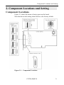
1
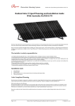
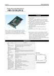
CNT24-4D(PCI)
24Bit Differencial Up/Down Counter Board
for PCI
User’s Guide
Copyright
Copyright 2000 CONTEC Co., LTD. ALL RIGHTS RESERVED
No part of this document may be copied or reproduced in any form
by any means without prior written consent of CONTEC Co., LTD.
CONTEC Co., LTD. makes no commitment to update or keep
current the information contained in this document.
The information in this document is subject to change without
notice.
All relevant issues have been considered in the preparation of this
document. Should you notice an omission or any questionable
item in this document, please feel free to notify
CONTEC Co., LTD.
Regardless of the foregoing statement, CONTEC assumes no
responsibility for any errors that may appear in this document nor
for results obtained by the user as a result of using this product.
Trademarks
MS, Microsoft, MS-DOS and Windows are trademarks of Microsoft
Corporation. Other brand and product names are trademarks of
their respective holder.
CNT24-4D(PCI)
i
Product Configuration
- CNT24-4D(PCI) Board…1
- CNT24-4D(PCI) SETUP DISK (3.5inch/1.44MB) …1
- User’s Guide (this booklet)…1
Unpacking:
This board is specially packed in an anti-static bag to prevent
damage in shipping.
Check the contents to make sure that you have everything listed
above. If you do not have all the items, contact your distributor
or CONTEC group office where you purchased.
Note!
Do not remove the board from its protective packaging until the
computer case is open and ready for installation. Electrical static
can cause damage to electrical components.
ii
CNT24-4D(PCI)
Table of Contents
Copyright ............................................................................i
Trademarks ........................................................................i
Product Configuration ..................................................... ii
1. Introduction ............................................................. 1
Features.........................................................................1
Limited Three-Year Warranty......................................2
How to Obtain Service..................................................2
Liability .........................................................................2
Handling Precautions...................................................3
About the Manual .........................................................4
2. Component Locations and Setting .............................. 5
Component Locations........................................................5
Setting the Board ID.........................................................6
Setting Procedure .........................................................6
Setting One-shot Pulse Output Signals...........................7
Setting Terminators ..........................................................8
3. Board Setup ............................................................. 9
Use CONTEC Windows Software Products.....................9
When Not Using CONTEC Software for Windows .......10
For Windows 98 Systems............................................10
For Windows 95 Systems............................................14
For other OS systems .................................................19
4. Connection with External Devices ............................ 21
Interface Connector.........................................................21
Connecting the Interface Connector ..........................21
Interface-Connector Signal Assignment....................22
PCB96WS and CCB-96 Signal Assignment ..............23
Connection of External Signals......................................24
Line Receiver Input Circuit and an Example
Connection...................................................................24
CNT24-4D(PCI)
iii
TTL-level Input Circuit
and an Example Connection ......................................25
Output Circuit and an Example Connection.............25
Example Connection with a Rotary Encoder.................27
Measures against Voltage Surges ..................................28
5. I/O Port Bit Assignment .......................................... 29
I/O Port Bit Assignment .................................................29
Setting Data ................................................................30
Count Flow ......................................................................31
Operation Commands .....................................................32
Description of Output Commands..................................34
Initial Count Value (Command CH0:00H:, CH1:05H:,
CH2:0AH:, CH3:0FH) .................................................34
Operation Mode (Command CH0:01H:, CH1:06H:,
CH2:0BH:, CH3:10H) .................................................34
Each Counter Operating Mode ..................................36
Phase Z/CLR Input (Command CH0:02H, CH1:07H,
CH2:0CH, CH3:11H)...................................................40
Compare Register (Command CH0:03H, CH1:08H,
CH2:0DH, CH3:12H) ..................................................41
Digital Filter (Command CH0:04H, CH1:09H,
CH2:0EH, CH3:13H) ..................................................42
Count Value Latch (Command 14H)..........................43
Interrupt Mask (Command 15H) ...............................44
Sense Reset (Command 16H) .....................................44
Programmable Timer (Command timer data:17H,
Timer start:18H) .........................................................45
One-shot Pulse (Command 19H)................................46
General-purpose Input Signal Select
(Command 1AH) .........................................................48
Description of Input Commands ....................................49
Count Read (Command CH0:00H, CH1:05H,
CH2:0AH, CH3:0FH) ..................................................49
Status Data (Command CH0:01H, CH1:06H,
CH2:0BH, CH3:10H) ..................................................49
Interrupt Mask (Command 15H) ...............................51
iv
CNT24-4D(PCI)
Sense Port (Command 16H) .......................................51
General-purse Input Signal Select
(Command 1AH) .........................................................52
Initialization....................................................................53
6. Board Specifications................................................ 55
Block Diagram.................................................................55
Specifications...................................................................56
7. Index ..................................................................... 59
CNT24-4D(PCI)
v
List of Figures
Figure 2.1.
Component Locations............................................... 5
Figure 2.2.
Board ID Settings (SW1).......................................... 6
Figure 2.3.
Switch for setting one-shot-pulse output signals ....... 7
Figure 2.4.
Terminator setting switches ...................................... 8
Figure 4.1.
Connecting the interface connector ........................ 21
Figure 4.2.
Connectors in use ................................................... 21
Figure 4.3.
Interface-connector signal assignment .................... 22
Figure 4.4.
PCB96WS and CCB-96 signal assignment ............. 23
Figure 4.5.
Line-receiver input circuit
and an example connection..................................... 24
Figure 4.6.
TTL-level input circuit and an example connection 25
Figure 4.7.
Open-collector output circuit and an example
connection .............................................................. 26
Figure 4.8.
TTL-level output circuit and an example connection26
Figure 4.9.
Example connection with a rotary encoder
(Line receiver input)............................................... 27
Figure 4.10. Example connection with a rotary encoder
(TTL input) ............................................................ 27
Figure 4.11. Example measures against voltage surges............... 28
Figure 5.1.
Output port ............................................................. 29
Figure 5.2.
Input port ............................................................... 29
Figure 5.3.
Count flow.............................................................. 31
Figure 5.4.
Example counting during 2-phase input.................. 36
Figure 5.5.
Example counting during single-phase input .......... 36
Figure 5.6.
Example counting during single-phase input
with gate control attached....................................... 37
vi
CNT24-4D(PCI)
Figure 5.7.
Example counting during synchronous clear .......... 37
Figure 5.8.
Example counting during asynchronous clear......... 38
Figure 5.9.
Example counting when count input multiplication
is set ....................................................................... 39
Figure 5.10. Phase Z enable frequency ZSEL=0
(Positive logic) ....................................................... 40
Figure 5.11. Digital filter............................................................ 42
Figure 6.1.
Block Diagram ....................................................... 55
CNT24-4D(PCI)
vii
List of Tables
Table 2.1.
One-shot-pulse output signal settings.......................... 7
Table 2.2. Terminator settings...................................................... 8
Table 5.1.
Output commands ..................................................... 32
Table 5.2. Input commands........................................................ 33
Table 5.3.
Counter operation modes .......................................... 35
Table 5.4. Switching counting directions ................................... 35
Table 5.5. Phase Z input mode................................................... 40
Table 5.6.
Digital filter clock settings ........................................ 43
Table 5.7.
Relationship between programmable timer setting data
and timer interrupt cycles.......................................... 46
Table 5.8.
Relationship between specified one-shot-pulse width
data and pulse widths ................................................ 47
Table 5.9. Initialized state.......................................................... 53
Table 6.1. Specifications............................................................ 56
viii
CNT24-4D(PCI)
Introduction
1. Introduction
Thank you for purchasing the CONTEC CNT24-4D(PCI).
The CNT24-4D(PCI) is a PCI bus-compliant interface that counts
digital signals from an external device. This board should be
inserted into a PC's PCI bus slot or PCI bus unit.
Read this guide thoroughly before you build a system including
creation of application programs and connection with external
devices.
Support software sold separately
- Driver Software Package (Option)
API-PAC(W32)
Please follow the setup instructions of the User’s manual shipped
with the software products and/or the help files of the package to
setup our interface board(s) to your system.
For details of CONTEC software products, please contact our sales
agencies.
Features
- The PCI bus-compliant interface board can be used with the PC98 series or PC-AT (DOS/V machines) equipped with a PCI bus
expansion slot.
- This single board can count up and down 24 bits for four
channels.
- The board can count two-phase signals of a rotary encoder or
linear gauge, for example.
- The board allows you to select a photocoupler insulated input or
TTL-level input for each channel.
- The board can either generate interrupts or output signals when a
count of each channel matches any specified value.
- The board is equipped with a programmable timer to allow
interrupts to be generated periodically according to a specified
timer value.
- The board is equipped with one general-purpose input signal for
each channel (both photocoupler and TTL).
CNT24-4D(PCI)
1
Introduction
Limited Three-Year Warranty
CONTEC Interface boards are warranted by CONTEC Co., LTD. to
be free from defects in material and workmanship for up to three
years from the date of purchase by the original purchaser.
Repair will be free of charge only when this device is returned
freight prepaid with a copy of the original invoice and a Return
Merchandise Authorization to the distributor or the CONTEC group
office, from which it was purchased.
This warranty is not applicable for scratches or normal wear, but
only for the electronic circuitry and original boards. The warranty
is not applicable if the device has been tampered with or damaged
through abuse, mistreatment, neglect, or unreasonable use, or if the
original invoice is not included, in which case repairs will be
considered beyond the warranty policy.
How to Obtain Service
For replacement or repair, return the device freight prepaid, with a
copy of the original invoice. Please obtain a Return Merchandise
Authorization Number (RMA) from the CONTEC group office
where you purchased before returning any product.
* No product will be accepted by CONTEC group without the
RMA number.
Liability
The obligation of the warrantor is solely to repair or replace the product.
In no event will the warrantor be liable for any incidental or
consequential damages due to such defect or consequences that arise
from inexperienced usage, misuse, or malfunction of this device.
2
CNT24-4D(PCI)
Introduction
Handling Precautions
Take the following precautions when handling this board.
- Never modify the board. The manufacturer cannot be
responsible for any board that has been modified by the user.
- Protect the board against shock and do not bend the board or it
will be damaged.
- Do not touch the gold-plated lines (edge connectors) on the board.
Touching causes poor contact. If you accidentally touch the
connectors, wipe it clean using industrial alcohol.
- The board has a switch that needs to be set before using the board.
Be sure to verify the switch before fitting the board into the slot.
- Always be sure to set the switches and jumpers on the board as
designated or it will fail.
- Always be sure to connect only the designated signals to the
connectors on the board or it will fail.
- Install the board in the PCI expansion slot in the PC.
- Do not insert or remove the board into or from the slot with the
PC turned on or the board will fail. Be sure to turn off either the
PC or the I/O expansion unit before inserting or removing the
board.
- The total current consumption of boards to be installed in the PCI
bus expansion slots of the PC must not exceed the power supply
capacity permitted to the PC.
CNT24-4D(PCI)
3
Introduction
About the Manual
This manual consists of the following chapters:
4
Chapter 1
Component Identification and Settings
Identifies each component of the board and explains
how to set the switch, for example.
Chapter 2
Setup
Explains how to set up the board to use it.
Chapter 3
Board Setup
Explains how to set up the board.
Chapter 4
Connection with External Devices
Explains the interface connector and connection
precautions.
Chapter 5
I/O Port Bit Assignment
Explains each I/O register which the board uses, bit
assignment, and bit definitions.
Chapter 6
Board Specifications
Explains the specifications and circuit block diagram.
CNT24-4D(PCI)
Component Locations and Setting
2. Component Locations and Setting
Component Locations
Figure 2.1 shows the names of major parts on the board.
Note that the switch setting shown below is the factory default.
Figure 2.1. Component Locations
CNT24-4D(PCI)
5
Component Locations and Setting
Setting the Board ID
When installing multiple CNT24-4D (PCI) boards in one PC, you
need to set their IDs in order to distinguish one board from another.
Each ID should be set to a unique value.
A board ID can be set in a range of 0 through F and 16 boards can
be distinguished at maximum.
When using only board, its factory setting (a board ID of 0) must be
used.
Setting Procedure
The board ID should be set with the rotary switch on the board.
Turn the SW1 twist knob to set the ID.
2
7 9
B C DE
A
3 4 56
SW1
BOARD ID
Factory setting
(board ID=0)
F 01
Figure 2.2. Board ID Settings (SW1)
6
CNT24-4D(PCI)
Component Locations and Setting
Setting One-shot Pulse Output Signals
ON
1 2 3 4
Set the type of one-shot-pulse output signals with SW2.
The TTL-level output or open collector output can be selected by
channel.
By referring to the following table, set the one-shot pulse output
signal.
Factory Setting: ON
SW2
Figure 2.3. Switch for setting one-shot-pulse output signals
Table 2.1. One-shot-pulse output signal settings
Bit
Channel
TTL-level output
Open-collector output
4
ch3
ON
OFF
3
ch2
ON
OFF
2
ch1
ON
OFF
1
ch0
ON
OFF
CNT24-4D(PCI)
7
Component Locations and Setting
Setting Terminators
Using SW3 through SW6, set whether or not to insert terminators.
SW6(ch0)
SW5(ch1)
SW4(ch2)
1 2 3 4
ON
1 2 3 4
ON
1 2 3 4
ON
ON
1 2 3 4
By referring to the following table, set whether or not to insert
terminators.
Factory Setting: ON
SW3(ch3)
Figure 2.4. Terminator setting switches
Table 2.2. Terminator settings
8
Bit
Input signal
Insert terminator
Do not insert terminator
4
General purpose (U)
ON
OFF
3
Phase Z
ON
OFF
2
Phase B
ON
OFF
1
Phase A
ON
OFF
CNT24-4D(PCI)
Board Setup
3. Board Setup
The board setup method varies according to the operating system
being used.
Use CONTEC Windows Software Products
For MS Windows OS systems, we recommend you to use our
Windows software products (optional).
< Examples of CONTEC software products for Windows>
- Driver Software Package (Option)
API-PAC(W32)
Please follow the setup instructions of the User’s manual shipped
with the software products and/or the help files of the package to
setup our interface board(s) to your system.
For details of CONTEC software products, please contact our sales
agencies.
CNT24-4D(PCI)
9
Board Setup
When Not Using CONTEC Software for Windows
When you don't use CONTEC software for Windows, the board
setup procedure varies with each OS.
For Windows 98 Systems
Every PCI bus board/device will be automatically assigned required
system resources, such as I/O address range and interrupt level, by
the system whenever the system is turned on.
Under Windows 98 OS, before using the board you should register
the board information, such as assigned resources, to the OS. This
procedure is called hardware installation. After the hardware
installation is done, Windows 98 can then manage the board
information from its registers.
Following is hardware installation steps. After finished the
installation, you are supposed to confirm the registered board
information from Windows 98 registers.
This procedure does not install board driver(s).
install driver program(s) yourself.
10
CNT24-4D(PCI)
Lately you should
Board Setup
Hardware Installation Steps
(1) Set the board ID.
(2) Be sure the power of the personal computer is turned off; then
plug the board into a PCI bus slot in the system.
(3) Turn the personal computer ON to start up Windows 98.
(4) Because this is the first time Windows 98 detected the board
from the system, Windows 98 will display a message of [New
Hardware] on the screen and start run an [Add New Hardware
Wizard] program. After you find a massage of [PCI
Multimedia Device] from the program window, click [Next>]
to continue.
(5) In the next dialog box, select a radio button of [Search for the
best driver for your device. (Recommended).], then click
[Next>] to continue.
(6) In the next dialog box, select both of the [Floppy disk drives
(F)] and [Specify Location (L)] check boxes, then enter the
drive name, such as "A:", and the directory name, WIN95, into
the [Location] field.
Insert the attached FD into the disk drive, then click [Next>] to
continue.
(7) In the [Windows driver file search for the device] dialog box,
check that "CONTEC Co., Ltd.-Board Name" and
"CNT_PI0.INF" in the [Location of driver] has been listed,
then click [Next>] to continue.
(8) In the next dialog box, you will find a message of "Windows
has finished installing the software that your new hardware
device requires." Then you click [Finish] to complete the
installation of the board. After completed the board
installation, you are supposed to confirm the registered board
information from Windows 98 registers. The "Checking
resources" part of this section explains you how to do it.
CNT24-4D(PCI)
11
Board Setup
Method of installing two or more boards:
(1) Install the first board correctly.
(2) Be sure to complete installation of the first board before
attempting to install a second one.
(3) Exit Windows 98 and turn the personal computer off.
(4) Set the board ID of the second board that should be different
from the first one. Then plug the board into a PCI bus slot.
(5) Turn the personal computer on and start the Windows 98 again.
(6) Windows 98 will display a massage of [New Hardware] on the
screen and start run an [Add New Hardware Wizard] program.
After you find a massage of [CONTEC Co., Ltd.-Board Name]
from the program window, click [Next>] to continue.
(7) In the next dialog box, select a radio button of [Display a list
of all the drivers in a specific location, so you can select the
driver you want.], then click [Next>] to continue.
(8) From the [Models] window, select "CONTEC Co., Ltd.Board Name" and click [Next>] to continue.
(9) In the [Windows driver file search for the device] dialog box,
there should be the message of "CONTEC Co., Ltd.-Board
Name" and "CONTEC~*.INF" in the [Location of driver]
window, after confirmed this message click [Next>] to
continue. (A number which is assigned by the OS will
replace the "*" mark.)
(10) In the next dialog box, you will find a message of "Windows
has finished installing the software that your new hardware
device requires." Then you click [Finish] to complete the
installation of the board. After completed the board
installation, you are supposed to confirm the registered board
information from Windows 98 registers again.
For installing the third board and any additional boards, follow the
same steps as those for installing a second board. Before you can
install a third board or additional boards, all the boards that are
already installed must be in their PCI bus slots.
12
CNT24-4D(PCI)
Board Setup
Notes!
- The second board cannot be properly installed unless the
resources (I/O addresses and interrupt level) for the board can
be allocated. Before attempting to install the second board,
first determine what PC resources are free to use.
- The resources used by each board do not depend on the location
of the PCI bus slot or the board itself. If you remove two or
more boards that have already been installed and then remount
one of them on the computer, it is unknown that which one of the
sets of resources previously assigned to the two boards is
assigned to the remounted board. In this case, you must check
the resource settings.
Checking resources
Follow the steps below to check the assigned resources managed by
the OS.
(1) Double-click on the [System] option in [Control Panel] to open
the [System Properties] property sheet. Select the [Device
Manager] tab.
(2) Click [Multi-function adapters] folder.
(3) Click [CONTEC Co., Ltd.-Board Name] folder to display its
properties.
(4) Select the [Resources] tab to check the device type, resource
settings, and the conflicting device list.
CNT24-4D(PCI)
13
Board Setup
For Windows 95 Systems
Every PCI bus board/device will be automatically assigned required
system resources, such as I/O address range and interrupt level, by
the system whenever the system is turned on.
Under Windows 95 OS, before using the board you should register
the board information, such as assigned resources, to the OS. This
procedure is called hardware installation. After the hardware
installation is done, Windows 95 can then manage the board
information from its registers.
Following is hardware installation steps. After finished the
installation, you are supposed to confirm the registered board
information from Windows 95 registers.
This procedure does not install board driver(s).
install driver program(s) yourself.
Lately you should
Procedure of Hardware Installation
<Checking the OS version>
The procedure of installing the board is different from the
Windows 95 versions. Before any installation, you must check the
version of Windows 95 that you are using.
(1) Open [Control Panel] from [My Computer].
(2) Double-click on the [System] option to open the [System
Properties] property sheet.
(3) Check the "System:" number displayed on the [General] page.
System :
Microsoft Windows 95
4.00.950
The versions of Windows 95 include 4.00.950, 4.00.950a,
4.00.950B and 4.00.950C. The board setup method depends on
the version of Windows 95 that is being used.
14
CNT24-4D(PCI)
Board Setup
For Windows 95 version 4.00.950 or 4.00.950a systems:
(1) Set the board ID.
(2) Be sure the power of the personal computer is turned off; then
plug the board into a PCI bus slot in the system.
(3) Turn the personal computer ON to start up Windows 95.
(4) Windows 95 will come up with the [New Hardware] detection
dialog box. Select [Multimedia Device: Select which driver
you want to install for your new hardware.] and then [Driver
from disk provided by hardware manufacturer].
(5) In the [Install From Disk] dialog box, insert the attached FD
into the disk drive, enter the drive name and directory name in
the [Copy Distributed File From] field, then click [OK].
This completes installation of the board.
(6) Follow the instructions on the screen to complete installation
of the board. After completed the board installation, you are
supposed to confirm the registered board information from
Windows 95 registers. The "Checking resources" part of this
section explains you how to do it.
For Windows 95 version 4.00.950B or 4.00.950C systems:
(1) Set the board ID.
(2) Be sure to check that the personal computer is off; then plug
the board into a PCI bus slot in the system.
(3) Turn the personal computer on to start up Windows 95.
(4) Because this is the first time Windows 95 detected the board
from the system, Windows 95 will display a message of [New
Hardware] on the screen and start run an [Device Driver
Wizard] program. After you find a massage of [PCI
Multimedia Device] from the program window, click [Next>]
to continue.
(5) In the next dialog box, select [Specify Location...]. Insert the
attached FD into a drive, enter the drive name and directory
name (WIN95) in the [Location] field, then click [OK].
(6) In the next dialog box, there should be a message of "Updated
driver found for this device". After confirmed this message
CNT24-4D(PCI)
15
Board Setup
you click [End]. This completes installation of the board.
After completed the board installation, you are supposed to
confirm the registered board information from Windows 95
registers. The "Checking resources" part of this section
explains you how to do it.
Method of installing two or more boards
(For Windows 95 version 4.00.950 or 4.00.950a system) :
(1) Install the first board correctly.
(2) Be sure to complete installation of the first board before
attempting to install the second one.
(3) Exit Windows 95 and turn the personal computer off.
(4) Check the board ID of the second board that should be
different from the first one. Then plug the board into a PCI
bus slot.
(5) Turn the personal computer on again to start up Windows 95.
(6) Windows 95 will come up with the [New Hardware] detection
dialog box. In [Multimedia Device: Select which driver you
want to install for your new hardware.], select [Select from
List].
(7) The [Select Hardware Type] dialog box will then appear.
In [Select Hardware Type to Install] windows, select [Other
Devices].
(8) In the [Select Device] dialog box, select [CONTEC] from
[Manufacturers] window and select [CONTEC Co., Ltd.-Board
Name] from [Models] window.
(9) A [Change System Settings] dialog box appears. Follow the
messages to restart the computer.
(10) When Windows 95 is restarted, installation of the second board
is completed. Check the assigned resources again.
For installing the third board and any additional boards, follow the
same steps as those for installing a second board. Before you can
install a third board or additional boards, all the boards that are
already installed must be in PCI bus slots.
16
CNT24-4D(PCI)
Board Setup
Notes!
- The second board cannot be properly installed unless the
resources (I/O addresses and interrupt level) for the board can
be allocated. Before attempting to install the second board,
first determine what PC resources are free.
- The resources used for each board do not depend on the location
of the PCI bus slot or the board itself. If you remove two or
more boards that have already been installed and then re-mount
one of them on the computer, it is unknown which one of the sets
of resources previously assigned to the two boards is assigned to
the re-mounted board. In this case, re-check the resource
settings.
Method of installing two or more Boards
(For Windows 95 version 4.00.950B or 4.00.950C systems) :
(1) Install the first board correctly.
(2) Be sure to complete installation of the first board before
attempting to install the second one.
(3) Exit Windows 95 and turn the personal computer OFF.
(4) Check the board ID of the second board, then plug it into a PCI
bus slot. Assign to the second board a board ID different
from the ID assigned to the first board.
(5) Turn the personal computer on again to start up Windows 95.
(6) The OS will then automatically install the second board.
When the installation has been completed, check the assigned
resources again.
For installing the third board and any additional boards, follow the
same steps as those for installing a second board. Before you can
install a third board or additional boards, all the boards that are
already installed must be in PCI bus slots.
Notes!
- The second board cannot be properly installed unless the
resources (I/O addresses and interrupt level) for the board can
be allocated. Before attempting to install a second board, first
determine which PC resources are free.
- The resources used for each board do not depend on the location
of the PCI bus slot or the board itself. If you remove two or
CNT24-4D(PCI)
17
Board Setup
more boards that have already been installed and then re-mount
one of them on the computer, it is unknown which one of the sets
of resources previously assigned to the two boards is assigned to
the re-mounted board. In this case, re-check the resource
settings.
Checking resources
Follow the steps below to check the assigned resources managed by
the OS.
(1) Double-click on the [System] option in [Control Panel] to open
the [System Properties] property sheet. Select the [Device
Manager] tab.
(2) Click on the [Multi-function adapters] folder.
(3) Click on the [CONTEC Co., Ltd.-Board Name] folder to
display its properties.
(4) Select the [Resources] tab to check the device type, resource
settings, and the conflicting device list.
18
CNT24-4D(PCI)
Board Setup
For other OS systems
We use MS-DOS as an example to show how to use the board under
other operation systems, in addition of the Windows OS.
Refer the MS-DOS programs in the attached FD.
For a PCI bus board, the system will automatically assign usable
resources to the board. Refer the following procedure to confirm
the assigned resources.
Procedure
(1) Set the board ID.
(2) Be sure that the personal computer is off; then plug the board
into a PCI bus slot in the personal computer.
(3) Turn the personal computer ON to start up MS-DOS.
(4) Copy the programs that are under the DOS directory of the
attached FD to a directory of your HDD.
(5) Execute the CNTPCI.EXE resource confirmation program.
(6) Check the I/O addresses and interrupt level (IRQ) displayed on
the screen.
Note!
When you use the board under a non plug-and-play OS like MSDOS, be sure that [PnP OS] is either [disabled] or set to [not to
use] in the PC's BIOS setup. If this is set to [Windows 95], for
example, the board might not be recognized properly.
CNT24-4D(PCI)
19
Board Setup
20
CNT24-4D(PCI)
Connection with External Devices
4. Connection with External Devices
Interface Connector
Connecting the Interface Connector
To connect the board with an external device, use the interface
connector on the board (CN1).
CN1
Figure 4.1. Connecting the interface connector
- Connector in use
Equivalent to the PCR-E96LMD (manufacturer: HONDA)
- Compatible connector
Equivalent to the PCR-E96FA (manufacturer: HONDA)
O p tion a l ca b le: P C B 9 6 W S -xx
A
C o n n e cto r:
E q u iv ale n t to
th e 1 7 JE -2 3 37 0 -02 (D 8 C )(D D K )
B
C o n n e ctor: P C R -E 9 6FA (m a n u fa ctu rer : H O N D A )
C a b le co ve r: P C SE 96 L K PA (m a n u fa ctu re r: H O N D A )
B4 8
B4 7
B2
B1
A48
A47
O ption a l ca b le : P C B 9 6 P S-xx + C on n ecto r co n ve rsio n b oa rd C C B -9 6
C on n e ctor:
E qu iva le n t to
th e D C L C -J 3 7 S A F -2 0 L9 (J A E )
A2
A1
C on n e ctor in s ta lle d
o n th e b oa rd:
E q u iva le n t to
th e P C R -E 9 6 L M D
(m a n u fac tu rer: H O N D A )
C C B -9 6
C o n n e ctor: P C R -E 9 6FA (m an u fa ctu rer : H O N D A )
C a b le co ve r: P C SE 96 L K PA (m a n u fa ctu rer : H O N D A )
"xx " r epre s en ts a ca b le le n gth (1 .5 m , 3 m or 5 m ).
Figure 4.2. Connectors in use
CNT24-4D(PCI)
21
Connection with External Devices
Interface-Connector Signal Assignment
Connect the board with an external device using the 96-pin
connector installed on the board.
Ground
C H 3 lin e r ece ive r ge n e ra l-pu rpos e in p u tC H 3 lin e re ceiv er ge n e ra l-pu rpos e in pu t+
C H 3 lin e r ece ive r Z ph as e in p u tCH 3 lin e rec eive r Z ph as e in pu t+
C H 3 lin e rece ive r B ph as e in p u tC H 3 lin e re ce ive r B ph as e in pu t+
C H 3 lin e re ceiv er A ph as e in p u tC H 3 lin e r ece iv er A ph as e in pu t+
C H 2 lin e r ece ive r ge n e ra l-pu rpos e in p u tC H 2 lin e re ceiv er ge n e ra l-pu rpos e in pu t+
C H 2 lin e receiver Z phase input-
CH2 line receiver Z phase input+
CH2 line receiver B phase inputCH2 line receiver B phase input+
CH2 line receiver A phase inputCH2 line receiver A phase input+
Ground
CH1 line receiver general-purpose inputCH1 line receiver general-purpose input+
CH1 line receiver Z phase inputCH1 line receiver Z phase input+
CH1 line receiver B phase inputCH1 line receiver B phase input+
CH1 line receiver A phase inputCH1 line receiver A phase input+
CH0 line receiver general-purpose inputCH0 line receiver general-purpose input+
CH0 line receiver Z phase inputCH0 line receiver Z phase input+
CH0 line receiver B phase inputCH0 line receiver B phase input+
CH0 line receiver A phase inputCH0 line receiver A phase input+
Ground
GND
GND
L3UL3U+
L3ZL3Z+
L3BL3B+
L3AL3A+
L2UL2U+
L2ZL2Z+
L2BL2B+
L2AL2A+
GND
GND
GND
GND
GND
GND
GND
GND
GND
GND
GND
GND
L1UL1U+
L1ZL1Z+
L1BL1B+
L1AL1A+
L0UL0U+
L0ZL0Z+
L0BL0B+
L0AL0A+
GND
GND
[4 9 ]
B 48
B 47
B 46
B 45
B 44
B 43
B 42
B 41
B 40
B 39
B 38
B 37
B 36
B 35
B 34
B 33
B 32
B 31
B 30
B 29
B 28
B 27
B 26
B 25
B 24
B 23
B 22
B 21
B 20
B 19
B 18
B 17
B 16
B 15
B 14
B 13
B 12
B 11
B 10
B 09
B 08
B 07
B 06
B 05
B 04
B 03
B 02
B 01
[9 6 ]
[1 ]
A48
A47
A46
A45
A44
A43
A42
A41
A40
A39
A38
A37
A36
A35
A34
A33
A32
A31
A30
A29
A28
A27
A26
A25
A24
A23
A22
A21
A20
A19
A18
A17
A16
A15
A14
A13
A12
A 11
A10
A09
A08
A07
A06
A05
A04
A03
A02
A01
[4 8 ]
N .C .
N .C .
T3U
T3Z
T3B
T3A
GND
T2U
T2Z
T2B
T2A
GND
OUT3
OUT2
OUT1
OUT0
N .C .
N .C .
N .C .
N .C .
GND
GND
GND
GND
GND
GND
GND
GND
N .C .
N .C .
T1U
T1Z
T1B
T1A
GND
T0U
T0Z
T0B
T0A
N .C .
GND
GND
GND
GND
GND
GND
GND
N .C .
Not connected
CH3TTL general-purpose input
CH3TTLZ phase input
CH3TTLB phase input
CH3TTLA phase input
Ground
CH2TTL general-purpose input
CH2TTLZ phase input
CH2TTLB phase input
CH2TTLA phase input
Ground
CH3 one-shot output
CH2 one-shot output
CH1 one-shot output
CH0 one-shot output
Not connected
Ground
Not connected
CH1TTL general-purpose input
CH1TTLZ phase input
CH1TTLB phase input
CH1TTLA phase input
Ground
CH0TTL general-purpose input
CH0TTLZ phase input
CH0TTLB phase input
CH0TTLA phase input
Not connected
Ground
Not connected
* [Pin numbers specified by HONDA]
Figure 4.3. Interface-connector signal assignment
22
CNT24-4D(PCI)
Connection with External Devices
PCB96WS and CCB-96 Signal Assignment
The optional cables and each corresponding signal are as shown
below:
PCB96WS's CNA and CCB96's CN3 (CNA)
Ground
Not connected
CH0TTLA phase input
CH0TTLB phase input
CH0TTLZ phase input
CH0TTL general-purpose input
Ground
CH1TTLA phase input
CH1TTLB phase input
CH1TTLZ phase input
CH1TTL general-purpose input
Not connected
GND
GND
GND
GND
GND
GND
GND
N.C.
T0A
T0B
T0Z
T0U
GND
T1A
T1B
T1Z
T1U
N.C.
N.C.
1
2
3
4
5
6
7
8
9
10
11
12
13
14
15
16
17
18
19
20
21
22
23
24
25
26
27
28
29
30
31
32
33
34
35
36
37
N.C.
N.C.
N.C.
OUT0
OUT1
OUT2
OUT3
GND
T2A
T2B
T2Z
T2U
GND
T3A
T3B
T3Z
T3U
N.C.
Not connected
CH0 one-shot output
CH1 one-shot output
CH2 one-shot output
CH3 one-shot output
Ground
CH2TTLA phase input
CH2TTLB phase input
CH2TTLZ phase input
CH2TTL general-purpose input
Ground
CH3TTLA phase input
CH3TTLB phase input
CH3TTLZ phase input
CH3TTL general-purpose input
Not connected
PCB96WS's CNB and CCB96's CN4 (CNB)
Ground
CH0 line receiver A phase input+
CH0 line receiver A phase inputCH0 line receiver B phase input+
CH0 line receiver B phase inputCH0 line receiver Z phase input+
CH0 line receiver Z phase inputCH0 line receiver general-purpose input+
CH0 line receiver general-purpose inputCH1 line receiver A phase input+
CH1 line receiver A phase inputCH1 line receiver B phase input+
CH1 line receiver B phase inputCH1 line receiver Z phase input+
CH1 line receiver Z phase inputCH1 line receiver general-purpose input+
CH1 line receiver general-purpose inputGround
Not connected
GND
L0A+
L0AL0B+
L0BL0Z+
L0ZL0U+
L0UL1A+
L1AL1B+
L1BL1Z+
L1ZL1U+
L1UGND
N.C.
1
2
3
4
5
6
7
8
9
10
11
12
13
14
15
16
17
18
19
20
21
22
23
24
25
26
27
28
29
30
31
32
33
34
35
36
37
GND
L2A+
L2AL2B+
L2BL2Z+
L2ZL2U+
L2UL3A+
L3AL3B+
L3BL3Z+
L3ZL3U+
L3UGND
Ground
CH2 line receiver A phase input+
CH2 line receiver A phase inputCH2 line receiver B phase input+
CH2 line receiver B phase inputCH2 line receiver Z phase input+
CH2 line receiver Z phase inputCH2 line receiver general-purpose input+
CH2 line receiver general-purpose inputCH3 line receiver A phase input+
CH3 line receiver A phase inputCH3 line receiver B phase input+
CH3 line receiver B phase inputCH3 line receiver Z phase input+
CH3 line receiver Z phase inputCH3 line receiver general-purpose input+
CH3 line receiver general-purpose inputGround
Figure 4.4. PCB96WS and CCB-96 signal assignment
CNT24-4D(PCI)
23
Connection with External Devices
Connection of External Signals
Line Receiver Input Circuit and an Example Connection
Figure 4.5. Line-receiver input circuit and an example
connection
Note!
The circuit for general-purpose input signals is also configured
similar to the above.
24
CNT24-4D(PCI)
Connection with External Devices
TTL-level Input Circuit and an Example Connection
External power
supply source
DC +5V
Board
Target equipment
+5V
LS541
+5V
Diode
Plus
common
10kΩ
Input pin
Internal
circuit
Diode
Ground
Output
pin
Minus
common
Figure 4.6. TTL-level input circuit and an example
connection
Notes!
- The circuit for general-purpose input signals is also configured
similar to the above.
- Keep the cable shorter than 1.5m.
- In order to prevent noise from causing malfunctions, keep the
circuit as far away as possible from other wires or noise sources.
Output Circuit and an Example Connection
When the count value of each channel matches any specified value,
the board outputs a one-shot match signal (for one pulse). The
SW2 allows you to select either open-collector output or TTL-level
output for the signal output section. If you opt for open-collector
output, you need an external power supply source.
CNT24-4D(PCI)
25
Connection with External Devices
Figure 4.7. Open-collector output circuit and an example
connection
Figure 4.8. TTL-level output circuit and an example
connection
Note!
The output transistor on this board does not come with a voltage
surge arrester. To drive an inductive load, such as a relay or a
lamp, you should provide measures against voltage surges on the
load side. For information on the countermeasures, see section,
"Measures Against Voltage Surges," in Chapter 3.
26
CNT24-4D(PCI)
Connection with External Devices
Example Connection with a Rotary Encoder
Figure 4.9. Example connection with a rotary encoder
(Line receiver input)
Figure 4.10. Example connection with a rotary encoder
(TTL input)
CNT24-4D(PCI)
27
Connection with External Devices
Measures against Voltage Surges
When connecting to the one-shot pulse output a load which causes a
voltage surge or rush current, such as an inductive load (relay coils)
or an incandescent bulb, you need to provide appropriate measures
in order to prevent the output stage from being damaged or from
malfunctioning due to noise. A rapid shut down of a coil, such as
a relay, causes a sudden high-voltage pulse to be generated. This
voltage, if it exceeds the output transistor's dielectric strength, may
cause the transistor to deteriorate leading to its breakdown. For
this reason, when driving an inductive load, such as a relay coil, be
sure to connect a surge suppressor. Example measures against
voltage surges are shown next:
Example when a relay coil is use
Diode
Relay coil
Output pin
Relay coil
Output pin
Zener diode
Ground
Ground
External supply voltage < Zener diode voltage
Example when a lamp is in use
Output pin
Output pin
Bypass resistor
for dim lighting
Rush current
preventive resistor
Ground
Ground
Figure 4.11. Example measures against voltage surges
Note!
If you decide to install a protective circuit, install it within a
distance of about 50cm from the load and contact. Otherwise the
circuit is not effective.
28
CNT24-4D(PCI)
I/O Port Bit Assignment
5. I/O Port Bit Assignment
I/O Port Bit Assignment
This board occupies I/O addresses for 32 continuous ports. Each
I/O port has a register. This group of registers is addressed by
command.
To set data in each of these registers, each command is output to the
set I/O address +0 port to enable an appropriate register to be set.
In the case of output, data is output to and set in the register using
the +1 port. In the case of input, data is read from the +1 port.
That is to say, regardless of whether the process is input or output, a
command is output to output port +0 to enable each register to be
set. Data is output with the +1 port in order to set the data in the
register or the register is read with the +1 port.
When setting data in each register, be sure to output a command to
output port +0 at all times even if the command is the same.
Figures 5.1 and 5.2 show I/O port bit assignments.
Figure 5.1. Output port
Figure 5.2. Input port
CNT24-4D(PCI)
29
I/O Port Bit Assignment
Setting Data
Normally, to set 8-bit data, a command is output to the +0 port and
data straight to the +1 port. However, in the case of 24-bit data,
the command is output first from the +0 port and then the +1 port is
output three times. At this time, the data is set in the order of
lower, middle and higher bytes. The +1 port is read three times to
read 24-bit data in the order of lower, middle and higher bytes.
In a similar manner, 32-bit data is set by outputting the +1 port four
times from the lower bytes.
30
CNT24-4D(PCI)
I/O Port Bit Assignment
Count Flow
Set initial
count
24-bit
up/down
counter
Count latch
(command 14H)
Readout
register
Read count
Command
CH0 : 00H
CH1 : 05H
CH2 : 0AH
CH3 : 0FH
Command
CH0 : 00H
CH1 : 05H
CH2 : 0AH
CH3 : 0FH
24-bit
comparator
Count
matches.
Match signal
Sense port
(Command 16H)
Interrupt mask
(Command 15H)
Set value to
compare
count with
Command
CH0 : 03H
CH1 : 08H
CH2 : 0DH
CH3 : 12H
Compare
register
Status data
Command
CH0 : 01H
CH1 : 06H
CH2 : 0BH
CH3 : 10H
One-shot pulse output
(Command 19H)
Figure 5.3. Count flow
CNT24-4D(PCI)
31
I/O Port Bit Assignment
Operation Commands
Table 5.1. Output commands
Command
[H]
D7
D6
D5
D4
RESET
SEL
ZSEL
02
UD/AB
DIR
Not in use
D1
D0
SEL2
SEL1
SEL0
ZE1
ZE0
0
Not in use
Function (bit)
CH0 initial count value (24)
CH0 value to compare count with
03
04
D2
CH0 initial count value
00
01
D3
CH0 operation mode (8)
CH0 phase Z/CLR input (3)
CH0 compare register (24)
Clock data for digital filter
CH0 digital filter (4)
05
Same as CH0
CH1 initial count value
06
Same as CH0
CH1 operation mode
07
Same as CH0
CH1 phae Z/CLR input
08
Same as CH0
CH1 compare register
09
Same as CH0
CH1 digital filter
0A
Same as CH0
CH2 initial count value
0B
Same as CH0
CH2 operation mode
0C
Same as CH0
CH2 phase Z/CLR input
0D
Same as CH0
CH2 compare register
0E
Same as CH0
CH2 digital filter
0F
Same as CH0
CH3 initial count value
10
Same as CH0
CH3 operation mode
11
Same as CH0
CH3 phase Z/CLR input
12
Same as CH0
CH3 compare register
13
Same as CH0
14
Not in use
CH3 digital filter
CH3 LT CH2 LT CH1 LT CH0 LT
Count value latch (4)
15
Not in use
TIME
CH3
CH2
CH1
CH0
Interrupt mask (5)
16
Not in use
TIME
CH3
CH2
CH1
CH0
Sense reset (5)
17
Programmable timer setting data
32
START
One-shot-pulse width data
19
1A
Timer data (32)
Not in use
18
Not in use
CH3
CH2
Timer start (1)
One-shot pulse (8)
CH1
CNT24-4D(PCI)
CH0
General-purpose input
signal select (4)
I/O Port Bit Assignment
Table 5.2.
Command
[H]
Input commands
D7
D6
D5
AI
Z
A
00
01
D2
D1
D0
B
1
U/D
EQ
U
AI
Z
A
B
1
Z
A
0F
B
1
CH0 status data (8)
CH1 count value (24)
U/D
EQ
U
U/D
EQ
U
CH2 count readout
AI
Function (bit)
CH0 count value (24)
CH1 count readout
0A
0B
D3
CH0 count readout
05
06
D4
CH1 status data (8)
CH2 count value (24)
CH3 count readout
CH2 status data (8)
CH3 count value (24)
10
AI
Z
A
B
1
U/D
EQ
U
CH3 status data (8)
15
0
0
0
TIME
CH3
CH2
CH1
CH0
Interrupt mask (5)
16
0
0
0
TIME
CH3
CH2
CH1
CH0
Sense port (5)
1A
0
0
0
0
CH3
CH2
CH1
CH0
General-purpose input
signal select (4)
CNT24-4D(PCI)
33
I/O Port Bit Assignment
Description of Output Commands
Initial Count Value
(Command CH0:00H:, CH1:05H:, CH2:0AH:, CH3:0FH)
Output a command to output port +0 and set an initial count value
with output port +1. Since the count data consists of 24 bits, the
data is divided by eight bits into three groups for output in the order
of lower, middle, and higher bits. When the third group (the
higher eight bits) is output, all 24-bit data is loaded onto the counter
at once.
The following is an example program to set an initial count value of
100 (64H) for CH0:
OUT Lead address +0H, 00H (select CH0 initial count value)
OUT Lead address +1H, 64H (lower)
OUT Lead address +1H, 00H (middle)
OUT Lead address +1H, 00H (higher)
Operation Mode
(Command CH0:01H:, CH1:06H:, CH2:0BH:, CH3:10H)
Output a command to output port +0 and set an operating mode
with output port +1.
RESET…………Clears the bit up/down counter to "000000H."
No counting takes place during RESET=0.
0 : Clear counter.
1 : Count
When the phase Z one-time input is enabled,
phase Z input enabled for one time is set again at
RESET = 0 that follows the clearing to zero.
SEL……………..Toggles pulse input to the counter.
0 : Line Receiver
1 : TTL-level input
34
CNT24-4D(PCI)
I/O Port Bit Assignment
ZSEL…………...Selects the phase Z-input logic
(positive/negative).
0 : Positive logic (HIGH active)
1 : Negative logic (LOW active)
UD/AB, SEL2-0……Selects a counter operating mode.
Table 5.3.
UD/AB
Operating mode set
SEL2
SEL1
SEL0
0
0
0
0
2-phase input, Synchronous clear, Multiply-by-one mode
0
0
0
1
2-phase input, Synchronous clear, Multiply-by-two mode
0
0
1
0
2-phase input, Synchronous clear, Multiply-by-four mode
0
1
0
0
2-phase input, Asynchronous clear, Multiply-by-one mode
1
0
1
2-phase input, Asynchronous clear, Multiply-by-two mode
1
1
0
2-phase input, Asynchronous clear, Multiply-by-four mode
1
0
1
1
Single-phase input, Asynchronous clear, Multiply-by-one mode
0
0
1
1
Single-phase input with gate control attached,
Asynchronous clear, Multiply-by-one mode
0
1
1
1
Single-phase input with gate control attached,
Asynchronous clear, Multiply-by-two mode
0
0
DIR
Counter operation modes
See
Table
5.4.
Table 5.4.
DIR
Switching counting directions
Rotary encoder's rotation direction
Clockwise
Counterclockwise
0
DOWN
UP
1
UP
DOWN
Note!
The initial state is set to 00H for all channels.
CNT24-4D(PCI)
35
I/O Port Bit Assignment
Each Counter Operating Mode
2-phase Input
Two-phase input is to input two pulses of phase A (the leading
signal) and phase B (the trailing signal) which differ by 90?.
When phase Z (the reference position signal) is available, the
counter can be cleared with 2-phase pulse input.
Phase A
(Phase A/UP)
Phase B
(Phase B/DOWN)
Phase Z
(Phase Z/CLR)
Count value
0
1
2
* The above represents counting operations when DIR is set to 1. When DIR
is set to 0, counting down takes place at the leading edge of phase A.
Figure 5.4. Example counting during 2-phase input
Single-phase Input
During single-phase input, input of an UP pulse results in counting
up while input of a DOWN pulse results in counting down. If UP
and DOWN pulses are simultaneously generated or both pulses
change to LOW, normal counting does not take place.
UP pulse
(Phase A/UP)
DOWN pulse
(Phase B/DOWN)
Count value
5
6
7
8
7
6
* The above represents counting operations when DIR is set to 1. When DIR is set to 0, counting
down takes place at the leading edge of the UP pulse and counting up takes place at the leading
edge of the DOWN pulse.
Figure 5.5. Example counting during single-phase input
36
CNT24-4D(PCI)
I/O Port Bit Assignment
Single-phase Input with Gate Control Attached
The counter can be started/stopped according to a gate control
signal input along with a series of single-phase pulses. A clear
signal clears the counter value to zero.
Figure 5.6. Example counting during single-phase input
with gate control attached
Synchronous Clear
When DIR and ZSEL are set to 1, the counter is cleared to zero at
the leading edge of phase A when the phase B input is set to low
and the phase Z input is set to high. Counting begins from the
leading edge of phase A that comes after the phase Z input is set to
low.
Figure 5.7. Example counting during synchronous clear
CNT24-4D(PCI)
37
I/O Port Bit Assignment
Asynchronous Clear
When DIR and ZSEL are set to 1, the counter is cleared to zero
when phase Z is set to high, regardless of phase A and B input
statuses. Regardless of phase Z input status, counting begins at
the next leading edge of phase A.
Phase A
(Phase A/UP)
Phase B
(Phase B/DOWN)
Phase Z
(Phase Z/CLR)
Count value
1
2
3
0
1
* When DIR is set to 0, counting down takes place at the leading edge of phase A when
phase B is set to low. When ZSEL is set to 0, counting down? is enabled when the
phase Z input is set to low.
Figure 5.8. Example counting during asynchronous clear
38
CNT24-4D(PCI)
I/O Port Bit Assignment
Multiplication of Count Input
Setting the count input multiplication setting to two or four times
enables you to fine-tune controlling.
Figure 5.9. Example counting when count input
multiplication is set
CNT24-4D(PCI)
39
I/O Port Bit Assignment
Phase Z/CLR Input
(Command CH0:02H, CH1:07H, CH2:0CH, CH3:11H)
Output a command to output port +0 and specify the phase Z-input
frequency with output port +1.
ZE1, ZE0….phase Z input mode selection
Table 5.5.
*
Phase Z input mode
Status specified
ZE1
ZE0
0
1
Disable the phase Z input. Set to this value when there is not phase Z.
1
0
Enable the next phase Z input only once.
1
1
Enable every phase Z input.
* represents the initial state.
Figure 5.10. Phase Z enable frequency ZSEL=0
(Positive logic)
40
CNT24-4D(PCI)
I/O Port Bit Assignment
Notes!
- The initial state is set to "enable the next phase Z input only
once" (04H).
- If ZSEL is set to 1 (negative logic), the frequency is enabled only
when the phase Z input is low.
- If you are not going to use the phase Z/CLR input, be sure to set
ZE1 to 0 and ZE0 to 1 (disable phase Z input).
- If you clear the count value by setting RESET=0, after having
cleared to zero with phase Z input while you are in "enable phase
Z input only once," "enable phase Z input only once" will be set
once more when RESET=0.
Compare Register
(Command CH0:03H, CH1:08H, CH2:0DH, CH3:12H)
Compare the count value of a corresponding channel with the
compare register value. If these two values match, set status bit
"EQ" to "0" (remains 0 as long as they are in agreement). This
register is initialized to 0H. Output the command to output port
+0 and set the value to compare the count against with output port
+1. Since the value to compare the count value against consists of
24 bits, output three times by 8 bits in the order of lower, middle,
and higher bits. The following is an example program to set the
value to compare counts against to 1000 (3E8H) on CH1:
OUT Lead address +0H, 03H (select CH1 compare register)
OUT Lead address +1H, E8H (lower)
OUT Lead address +1H, 03H (middle)
OUT Lead address +1H, 00H (higher)
One-shot pulses can also be output depending on settings (see
section, "One-shot Pulse").
CNT24-4D(PCI)
41
I/O Port Bit Assignment
Digital Filter
(Command CH0:04H, CH1:09H, CH2:0EH, CH3:13H)
D6
D7
D5
D4
D3
Not in use
04H/09H/0EH/13H
D2
D1
D0
Clock data for digital filter
The digital filter allows the counter to operate normally even when
noise enters into pulses input to the counter and/or into A-, B-, and
Z-phase signals. The sampling cock cycle of the digital filter is
determined by clock setting data for the digital filter.
When the input signal is sampled with this sampling clock and if
HIGH (or LOW) is detected for a duration of four continuous
clocks, the digital filter outputs HIGH (or LOW) and communicates
it to the counter circuit.
Output the command to output port +0 and set a sampling cycle
with output port +1. The cycle can be set in a range of 0.1µsec
through 1,056.1µ sec.
All externally input signals (except for general-purpose input
signals) are fetched through the digital filter into the internal
counter. They are fetched after a delay of four set-sampling-cycle
clocks.
When initialized, externally input signals are fetched after a delay
of 0.4µ sec.
Externally
input signal
Digital filter
Input to the PC
Four set-sampling-cycle clocks
Externally
input signal
Not valid
Input to the PC
* The same applies also to the LOW level.
Figure 5.11. Digital filter
42
CNT24-4D(PCI)
Valid
I/O Port Bit Assignment
Table 5.6.
Digital filter clock settings
D3
D2
D1
D0
Digital filter
clock cycle
0
0
0
0
0.1µ sec
Approx. less than 1MHz
0
0
0
1
6.5µ sec
Approx. less than 15kHz
0
0
1
0
25.7µ sec
Approx. less than 3.5kHz
0
0
1
1
32.1µ sec
Approx. less than 3kHz
0
1
0
0
204.9µ sec
Approx. less than 480Hz
0
1
0
1
211.3µ sec
Approx. less than 470Hz
0
1
1
0
230.5µ sec
Approx. less than 430Hz
0
1
1
1
236.9µ sec
Approx. less than 420Hz
1
0
0
0
819.3µ sec
Approx. less than 122Hz
1
0
0
1
825.7µ sec
Approx. less than 121Hz
1
0
1
0
844.9µ sec
Approx. less than 118Hz
1
0
1
1
851.3µ sec
Approx. less than 117Hz
1
1
0
0
1024.1µ sec
Approx. less than 97Hz
1
1
0
1
1030.5µ sec
Approx. less than 96Hz
1
1
1
0
1049.7µ sec
Approx. less than 95Hz
1
1
1
1
1056.1µ sec
Approx. less than 94Hz
Input frequency
Accuracy with respect to a set cycle is approximately ±1/10,000.
Notes!
- The initial state is set to 0.1m sec. (When the cycle is not
specified, the cycle also defaults to 0.1m sec.)
- A delay of more than four set-cycle clocks may occur depending
on noise.
- If a level changes at a frequency faster than the set-samplingclock cycle, that level change is invalidated and not correctly
counted. Be sure to input signals which are less than the input
frequency.
Count Value Latch (Command 14H)
D7
14H
D6
D5
Not in use
D4
D3
D2
D1
D0
CH3 LT CH2 LT CH1 LT CH0 LT
Latch the count value of a corresponding channel to the readout
register. Output 14H to output port +0 and set the data latch
setting with output port +1. When the appropriate bit is set to "1,"
the count value is latched. Setting all appropriate bits to "1"
allows simultaneous latching for all channels.
Note!
The initial state is set to "do not latch" (00H).
CNT24-4D(PCI)
43
I/O Port Bit Assignment
Interrupt Mask (Command 15H)
D6
D7
15H
D5
Not in use
D4
D3
D2
D1
D0
TIME
CH3
CH2
CH1
CH0
Output 15H to output port +0 and set the mask with output port +1.
Setting an appropriate bit to "1" inhibits interrupt signals to be
generated.
TIME
Set to "1" to inhibit interrupts to be generated
when the time set on the programmable timer
elapses. Set to "0" to cancels the inhibition of
interrupts.
CH3-CH0
Correspond to each channel. Set each to "1" to
inhibit interrupts to be generated when the count
matches. Set to "0" to cancel the inhibition of
interrupts.
Note!
- The initial state is set to mask all channels with the timer (1FH).
- Even in masked state, each channel's count match and timer's
time-up statuses do change.
Sense Reset (Command 16H)
D6
D7
16H
Not in use
D5
D4
D3
D2
D1
D0
TIME
CH3
CH2
CH1
CH0
During interrupt sensing an appropriate bit is set to "1" when the
count of each channel matches or when the time set on the timer
expires. If the appropriate bit is set to "1," no interrupt signal is
generated when the count matches or the set time expires the next
time. Output of 16H to output port +0 and output of "1" to the
appropriate bit of output port +1 clear the sense bit, allowing the
next interrupt signal to be generated.
44
TIME
Resets the sense bit when the time set on the
programmable timer expires.
CH3-CH0
Reset the count match sense bit of each channel.
CNT24-4D(PCI)
I/O Port Bit Assignment
Programmable Timer
(Command timer data:17H, Timer start:18H)
D7
D6
17H
D7
18H
D5
D4
D3
D2
D0
D1
Programmable timer setting data
D6
D5
D4
D3
D2
D0
D1
Not in use
START
The programmable timer can generate interrupts at cycles according
to 32-bit setting data. To operate with the timer, you need to set 32
data and set the START bit to "1."
To set the programmable timer, output 17H with output port +0 and
set timer data with output port +1. Since the timer data consists of
32 bits, output the data by 8 bits four times, starting from the lower
bits. The timer can be set in a range of 1msec through 200sec.
To start the timer output timer start command 18H with output port
+0 and set an appropriate bit to "1" with output port +1. To stop
the timer, set this bit to "0."
The relationship between programmable timer setting data and
timer interrupt cycles is as shown in Table 5.7. The following is
an example program to set the programmable timer to one second.
OUT Lead address +0H,
17H (select timer setting)
OUT Lead address +1H, FFH (least significant)
OUT Lead address +1H,
2CH (lower)
OUT Lead address +1H,
31H (higher)
OUT Lead address +1H,
01H (most significant)
OUT Lead address +0H,
18H (select timer start)
OUT Lead address +1H,
1H (timer start)
Note!
When initialized, the timer is stopped.
CNT24-4D(PCI)
45
I/O Port Bit Assignment
Table 5.7.
Relationship between programmable timer setting
data and timer interrupt cycles
Programmable timer setting data [H]
Higher bytes
Lower bytes Timer interrupt cycle
0
0
0
0
4
E
1
F
1msec
0
0
0
3
0
D
3
F
10msec
0
0
1
E
8
4
7
F
100msec
0
1
3
1
2
C
F
F
1sec
0
2
6
2
5
9
F
F
2sec
0
3
9
3
8
6
F
F
3sec
0
4
C
4
B
3
F
F
4sec
0
5
F
5
E
0
F
F
5sec
0
7
2
7
0
D
F
F
6sec
0
8
5
8
3
A
F
F
7sec
0
9
8
9
6
7
F
F
8sec
0
A
B
A
9
4
F
F
9sec
0
B
E
B
C
1
F
F
10sec
1
1
E
1
A
2
F
F
15sec
1
7
D
7
8
3
F
F
20sec
2
3
C
3
4
5
F
F
30sec
2
F
A
F
0
7
F
F
40sec
3
B
9
A
C
9
F
F
50sec
7
7
3
5
9
3
F
F
100sec
B
2
D
0
5
D
F
F
150sec
E
E
6
B
2
7
F
F
200sec
Accuracy with respect to a set cycle is approximately ±1/10,000.
One-shot Pulse (Command 19H)
When the count value of each channel matches the value to
compare against, one-shot pulses are individually output to each
channel. The width of these pulses is the same for all channels
and is determined by set data. The width can be set in a range of 0
through 104.45msec.
Output +19H to output port +0 and set the pulse width with output
port +1.
46
CNT24-4D(PCI)
I/O Port Bit Assignment
The one-shot pulse width can be found by the following formula:
Table 5.8. Relationship between specified one-shot-pulse width
data and pulse widths
One-shot-pulse width setting data
D7
*
Pulse width
D0
[H]
0
0
0
0
0
0
0
0
00H
0
0
0
0
0
0
0
1
01H
Approx.409.6µ sec
0
0
0
0
0
0
1
0
02H
Approx.819.2µ sec
0
0
0
0
0
0
1
1
03H
Approx. 1.23msec
0
0
0
0
1
1
0
0
0CH
Approx. 4.92msec
0
0
0
1
1
0
0
1
19H
Approx. 10.24msec
0
0
1
1
0
0
0
1
31H
Approx. 20.07msec
0
1
0
0
1
0
0
1
49H
Approx. 29.9msec
0
1
1
0
0
0
1
0
62H
Approx. 40.14msec
0
1
1
1
1
0
1
0
7AH
Approx. 49.97msec
1
0
0
1
0
0
1
1
93H
Approx. 60.2msec
1
0
1
0
1
0
1
1
ABH
Approx. 70.04msec
1
1
0
0
0
1
0
0
C4H
Approx. 80.28msec
1
1
0
1
1
1
0
0
DCH
Approx. 90.11msec
1
1
1
1
0
1
0
1
F5H
Approx. 100.35msec
1
1
1
1
1
1
1
1
FFH
Approx. 104.45msec
0
* represents the initial state.
Notes!
- The initial state is set to "pulse width=0 (do not output) (00H).
- Pulse widths may slightly vary depending on the specifications of
a connected load.
CNT24-4D(PCI)
47
I/O Port Bit Assignment
General-purpose Input Signal Select (Command 1AH)
D7
1AH
D6
D5
Not in use
D4
D3
D2
D1
D0
CH3
CH2
CH1
CH0
This command selects line receiver input or TTL input for the
general-purpose input signals of a corresponding channel when line
receiver input is in use. Output 1AH to output port +0 and set the
input signal with output port +1. Set an appropriate bit to "0" to
opt for line receiver input or to "1" to opt for TTL input.
Note!
The initial state is set to "line-receiver input (00H)."
48
CNT24-4D(PCI)
I/O Port Bit Assignment
Description of Input Commands
Count Read
(Command CH0:00H, CH1:05H, CH2:0AH, CH3:0FH)
Count values are read by reading readout register contents of a
corresponding channel. Output the command to output port +0
and read input port +1 three times. This allows the lower, middle,
and higher bits of the count value to be read.
When initialized, the contents of the readout register are not
defined.
The following is an example program to read the CH2 count value:
OUT Lead address +0, 0AH (select the CH2 count value.)
IN
Lead address +1, (lower)
IN
Lead address +1, (middle)
IN
Lead address +1, (higher)
In this case, you need to set the CH2 count-value latch to "1" in
advance.
Status Data
(Command CH0:01H, CH1:06H, CH2:0BH, CH3:10H)
Output the command to output port +0 and read input port +1.
This allows you to monitor each signal input, counting direction,
count matching and abnormal input statuses.
AI ……………...This bit is set to "1" to indicate an abnormal pulse
input if a simultaneous change of phases A and B
is detected during 2-phase input or a simultaneous
change of UP and DOWN pulses is detected
during up/down input.
1 : Detect abnormal input.
0 : Do not detect abnormal input.
Z ………………..Indicates phase Z input status.
CNT24-4D(PCI)
49
I/O Port Bit Assignment
< When set to positive logic:>
1 : Phase Z input status [1]
0 : Phase Z input status [0]
<When set to negative logic: >
1 : Phase Z input status[0]
0 : Phase Z input status[1]
A……………….Indicates phase A input status.
1 : Phase A input status[1]
0 : Phase A input status[0]
B……………….Indicates phase B input status.
1 : Phase B input status[1]
0 : Phase B input status[0]
U/D…………….Count-direction operating status
This status bit indicates the direction in which the
current up/down counter is operating.
0 : Engaged in counting up.
1 : Engaged in counting down.
EQ……………...Detects and outputs match or mismatch.
0 : The count value matches compare register's
contents.
1 : The count value does not match compare
register's contents.
U………………..Indicates the general-purpose input status.
1 : General-purpose input status[1]
0 : General-purpose input status[0]
Notes!
- The initial state varies with external connection states.
- A, B, and Z phase statuses lag by four cyclical clocks since the
status data is available after the filter function is processed.
The general-purpose input status indicates the external input
status as it is.
- The Z-phase logic must be set with the "ZSEL" operating mode
setting.
50
CNT24-4D(PCI)
I/O Port Bit Assignment
Interrupt Mask (Command 15H)
This command allows you to monitor the current interrupt-mask
status which has been set with the interrupt mask command.
TIME corresponds to the programmable timer and CH3 through
CH0 correspond to each channel. If these bits are all set to "1,"
interrupts are masked and they will not be output.
Output 15H to output port +1 and read input port +1. This allows
you to monitor the mask status.
0 : Do not mask
1 : Mask
Note!
The initial state is set to 1FH.
Sense Port (Command 16H)
Indicates the count match status of each channel and time-up status.
Output 16H to output port +0 and read input port +1.
you to monitor sense port status.
This allows
-TIME…………When the time set on the programmable timer
expires, this bit is set to "1."
-CH3-CH0……..If the up/down counter matches compare register's
contents for each of CH3 through CH0, the bit for
each corresponding channel is set to "1." When
counting is implemented for multiple channels and
an interrupt is generated with a match signal, you
can identify the channel from which the interrupt
is generated.
0 : The count value does not match.
Wait until the time expires.
1 : The count value matches. Time is up.
CNT24-4D(PCI)
51
I/O Port Bit Assignment
Notes!
- The initial state is set to 00H.
- If an interrupt occurs when interruption is set and TIME or any
bit from CH3 through CH0 is set to "1," the next interrupt is not
generated unless the appropriate sense bit is reset. For
information on how to reset the sense bit, see "Sense Reset" for
the output port.
General-purse Input Signal Select (Command 1AH)
1AH
D7
D6
D5
D4
D3
D2
D1
D0
0
0
0
0
CH3
CH2
CH1
CH0
You can monitor the general-purpose input signal of a
corresponding channel to find whether it is set to line receiver or to
TTL input, when line receiver input is in use. To monitor the
setting, output 1AH to output port +0 and read input port +1.
0: Line-receiver input
1: TTL-level input
Note!
The initial state is set to 00H.
52
CNT24-4D(PCI)
I/O Port Bit Assignment
Initialization
When the board is turned on or reset, it is initialized to the state
shown next:
Table 5.9.
Initialized state
Parameter
Initial setting
Operating mode
00H
Phase Z/CLR input
04H (Enable phase Z only once)
Compare register
0
Readout register
Not defined
24-bit up/down counter
000000H
Digital filter
00H (0.1 msec)
Status data
7BH (When no external device is connected.)
Count latch
00H
Interrupt mask
1FH (Inhibit all interrupts)
Sense port
00H
Timer data
00000000H
Timer start
00H (Stop the timer)
One-shot pulse
00H (Do not output)
General-purse Input Signal Select
00H (Line Receiver Input)
CNT24-4D(PCI)
53
I/O Port Bit Assignment
54
CNT24-4D(PCI)
Board Specifications
6. Board Specifications
Block Diagram
16-bit, sampling-clock counter for
digital filter
PCI Bus
Buffer
Selector
24-bit counter
Digital filter
PCI Bus Interface
24-bit readout register
Line-receiver
input x 4 channels
TTL-level
input x 4 channels
24-bit comparator
24-bit compare register
One-shot pulse output
One-shot pulse
output x 4 channels
(TTL-level output or
open-collector output
can be selected.)
20MHz
system
clock
CNT24-4D(PCI)
Figure 6.1. Block Diagram
CNT24-4D(PCI)
55
Board Specifications
Specifications
Table 6.1.
Specifications
Item
Specification
Counter input section,
Channel count
4
Counting system
Up/down counting
Max. count
FFFFFFH (binary data)
Input type
Line-receiver input or TTL-level input
Input signal
Phase A/UP
One x 4 channels
Phase B/DOWN
One x 4 channels
Phase Z/CLR
One x 4 channels
General-purpose input
One x 4 channels
Element in use
Equivalent to the AM26LS32 (T.I)
Terminating resistance
100Ω (Can be disconnected by switch.)
Line receiver input section
TTL-level input section
Response frequency
Receiver input sensitivity
±200mV
In-phase input voltage range
± 7V
Signal extension distance
1,200m (dependent on wiring environment and input
frequency)
Element in use
Equivalent to the 74LS541 (T.I)
Signal extension distance
1.5m (dependent on wiring environment)
Line-receiver input: Max 1 MHz 50% duty
TTL-level input: Max 1 MHz
50% duty
Interrupt
One. Generated when each channel count matches or the timer runs out of time.
Digital filter
0.1µ sec - 1056.1µ sec (can be independently set for each channel.)
Timer
1msec - 200sec
Match-signal output
Output count
One x 4 channels
Output type
Uninsulated open-collector output or TTL-level output (Selectable by a switch.)
Rated output
Max 50VDC, 90mA (per 1 point)
Signal output width
0~104.45msec (Same for all channels)
Response rate
Max. 5µsec
Signal extension distance
1.5m (dependent on wiring environment)
Output protection network
Not available
Common parameters
I/O address
32 port occupation
Current consumption
5VDC Max.500mA
Operating conditions
0-50ºC, 20-90% humidity (no condensing)
External dimensions (mm)
176.4(L)×107.0(H)
Weight
120g
56
CNT24-4D(PCI)
Board Specifications
External Dimensions
107.0
176.4
[mm]
CNT24-4D(PCI)
57
Board Specifications
58
CNT24-4D(PCI)
Index
7. Index
B
Board ID, 6
L
Liability, 3
Board Setup, 9
O
C
Obtain Service, 3
Checking resources, 13, 18
Component Locations, 5
S
Setup, 5
F
Support software, 1
Features, 1
S
H
Handling Precautions, 3
Warranty, 2
Windows 95, 14
Windows 98, 10
I
Introduction, 1
CNT24-4D(PCI)
59
A-46-458
LZT0761
021018[001129]
CONTEC Group
JAPAN
: Headquarters
CONTEC Co., LTD.
3-9-31, Himesato, Nishiyodogawa-ku, Osaka 555-0025, Japan
Tel
: +81 (6) 6477-5219
Fax : +81 (6) 6477-1692
E-mail
: [email protected]
U.S.A.
: CONTEC MICROELECTRONICS U.S.A. INC.
744 South Hillview Drive, Milpitas, CA 95035 U.S.A.
Tel
: +1 (408) 719-8200
Fax : +1 (408) 719-6750
E-mail
: [email protected]
EUROPE
: CONTEC MICROELECTRONICS EUROPE B.V.
Binnenweg 4, 2132 CT, Hoofddorp, The Netherlands
Tel
: +31 (23) 567-3030
Fax : +31 (23) 567-3035
E-mail
: [email protected]
KOREA
: HYOJIN CONTEC Co., LTD.
Ki-im Bldg. #399, Shindolim-Dong, Kuro-ku, Seoul, Korea
Tel
: +82 (2) 2636-4277/8
Fax : +82 (2) 2636-4279
E-mail
: [email protected]
CHINA
:
INTERNATIONAL CONTEC TECHNOLOGY CO., LTD.
B-8F, Hua Tong Building, No. B19, Che Gong Zhuang West Road,
Hai Dian District, Beijing 100044, China
Tel
: +86(10)8801-8228
Fax : +86 (10)8801-8209
E-mail
: [email protected]
SHANGHAI CONTEC MICROELECTRONICS CORP.
No. 481 Gui Ping Road, Cao He Jing Hi-Tech Park Shanghai, 200233, China
Tel
: +86 (21) 6485-1907
Fax : +86 (21) 6485-0330
E-mail
: [email protected]
SHENYANG CONTEC MICROELECTRONICS Co., LTD.
No. 169, Qingnian Street, Shenhe District, Shenyang 110015, China
Tel
: +86 (24) 2392-9771
Fax : +86 (24) 2392-9773
TAIWAN
: MACROMATE CORP.
8F, Universal Center, No.179, Ta-Tung Rd., Sec.1 Hsi-Chih, Taipei Hsien, Taiwan,
R.O.C
Tel
: +886 (2) 2647-9353
Fax : +886 (2) 2647-9373
E-mail
: [email protected]
A-46-368
Ver. 2001. 02. 06