1
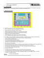
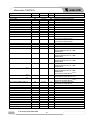
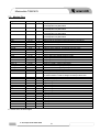
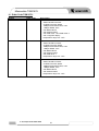
Minimodule TQM167U
TQ-Minimodul
TQM167U
mit
Microcontroller SAB-C167
Hardware - Manual
© TQ components GmbH 2002
Minimodule TQM167U
Hardware Manual for:
TQM167U
Rev100
Rev102
Rev103
Rev104
Rev105
Rev106
Rev107
Rev108
TQ-Components reserves the right to make changes without further notice to any products herein. TQ-Components
makes no warranty, representation or guarantee regarding the suitability of its products for any particular purpose,
nor does TQ-Components assume any liability arising out of the application or use of any product or circuit, and
specifically disclaims any liability at all, including without limitation consequential or incidental damages. „Typical“
parameters which may be provided in TQ-Components data sheets and/or specifications can and do vary in different
applications and actual performance may vary over time. All operating parameters, including „Typicals“ must be
validated for each customer application by customer’s technical experts. TQ-Components does not convey any
license under its patent rights nor the rights of others. TQ-Components products are not designed, intended, or
authorised for use as components in systems intended for surgical implant into the body, or other applications
intended to support or sustain life, or for any other application in which failure of the TQ-Components product could
create a situation where personal injury or death may occur. Should a buyer purchase or use TQ-Components
products for any such unintended or unauthorised application, a buyer shall indemnify and hold TQ-Components and
its officers, employees, subsidiaries, affiliates, and distributors harmless against all claims, costs, damages, and
expenses, and reasonable attorney fees arising out of, directly or indirectly, any claim of personal injury or death
associated with such unintended or unauthorised use, even if such claim alleges that TQ-Components was negligent
regarding the design or manufacture of the part. TQ-Components is registered trademark of TQ-Components
GmbH.
Reproduction, in part or whole, without the prior written consent of TQ-Components GmbH is prohibited.
© TQ components GmbH 2002
2
Minimodule TQM167U
Contents
Pragraph
Number
Title
1
2
Page
Number
Introduction ...................................................................................................................................................4
Block-Diagram ..............................................................................................................................................5
2.1 Microcontroller SAB-C167CR-LM / SAB-C167CS-32FM .......................................................................5
2.2 Memory...................................................................................................................................................6
2.2.1 Flash-Memory..................................................................................................................................6
2.2.2 SRAM-Memory ................................................................................................................................6
2.2.3 Serials EEPROM .............................................................................................................................6
2.3 Reset-Logic.............................................................................................................................................6
2.4 Interface ..................................................................................................................................................6
2.4.1 Serial-Interface ................................................................................................................................6
2.4.2 CAN-Interface..................................................................................................................................6
2.4.3 Bus-Interface ...................................................................................................................................6
2.4.4 Internal Bootstrap Loader ................................................................................................................6
2.5 XREG......................................................................................................................................................6
2.6 7Segment Display...................................................................................................................................6
2.7 Internal LED ............................................................................................................................................7
3
Microcontroller ..............................................................................................................................................7
4
Memory.........................................................................................................................................................8
4.1 Flash-Memory.........................................................................................................................................8
4.1.1 Flash-Memory structure...................................................................................................................8
4.1.2 Flash EPROM BUSCON .................................................................................................................9
4.2 SRAM-Memory .......................................................................................................................................9
4.2.1 SRAM-Memory structure .................................................................................................................9
4.2.2 SRAM access times ......................................................................................................................10
4.3 SerialsEEPROM ...................................................................................................................................11
4.4 Memory Management...........................................................................................................................11
4.4.1 Principle of operation.....................................................................................................................11
4.4.2 Chip Select allocation ....................................................................................................................11
4.4.3 Programming of the Chip Select lines ...........................................................................................12
4.4.4 Programming the SYSCON registers............................................................................................13
4.4.5 Programming the XREG/External UART.......................................................................................14
4.4.6 Programming the flash EPROMs ..................................................................................................15
4.4.7 Examples of memory configurations .............................................................................................15
5
Interface......................................................................................................................................................16
5.1 Serial Interface......................................................................................................................................16
5.1.1 Internal asynchronous interface ....................................................................................................16
5.1.2 Internal synchronous interface ......................................................................................................16
5.1.3 External asynchronous interface ...................................................................................................17
5.2 CAN - Interface .....................................................................................................................................17
5.3 Bus - Interface ......................................................................................................................................17
5.4 Internal bootstrap loader.......................................................................................................................17
6
Power supply ..............................................................................................................................................18
6.1 Supply voltage ......................................................................................................................................18
6.2 Maximum supply current.......................................................................................................................18
7
Pin Configuration ........................................................................................................................................19
7.1 CPU Pins ..............................................................................................................................................19
7.2 Module Pins ..........................................................................................................................................22
8
Mechanical Data.........................................................................................................................................23
8.1 Connector .............................................................................................................................................23
8.2 Connector Position ...............................................................................................................................23
9
Pin Configuration ........................................................................................................................................24
9.1 Mechanikal Drawing .............................................................................................................................25
10 Order Code TQM167U: ..............................................................................................................................26
11 References .................................................................................................................................................28
© TQ components GmbH 2002
3
Minimodule TQM167U
1 Introduction
TQ embedded Microcontroller Systems
High integration and high reliability are what set the TQ-Components industrial microcontroller modules
apart from the rest. TQ-Components Minimodules from credit-card to half credit-card size are
unbeatable in various applications. With an ever-expanding product line and clear technology migration
path, TQ-Components offers OEMs uncompromising excellence in microcontroller modules. In a
variety of industrial measurement, process regulation and control developments engineers confronted
with the task of developing a complex monitoring / control system under time constraints are the prime
beneficiaries of our microcontroller devices. Compare the advantage of the implementing a TQComponents module to the total cost of a completely new circuitry design.
Time to market
TQ-Components microcontroller modules provide a drop-in CPU solution, with complete CPU kernel
functionality on board. This enables engineers to take a project from concept to prototype or market in
weeks, rather than in months or longer.
Reliability
TQ-Components modular embedded microcontroller Minimodules have proven to be reliable and
rugged in numerous demanding and critical applications. Our highly knowledgeable team of electronic
engineers has wide experience in designing embedded microcontroller Modules. The team‘s
commitment to quality and reliability is evident throughout the whole TQ-Components product line.
Upgradability
Thanks to the flexibility of TQ’s product architectures, you will be able to enhance your products by
taking advantage of a new technology as when it becomes available. Our products offer a migration
path so you can upgrade features or performance without major redesign.
TQ-Minimodules offers you ...
þ Best price-performance relationship
§
§
§
uncompromising use of most modern production-technology
low price through high production quantity
Customised Versions on requests
þ Maximum performance on small footprint
§
§
§
§
double-sided SMT Technology
Fine Pitch Multilayer Printed Circuit Boards
using latest chip technology
using latest Flash Memory technology
þ save time and money in your development
§
§
§
§
complete CPU kernel functionality on board
immediate start through particular monitor-program
works with most modern Software Development Tools such as compilers and debuggers
Design-In Support through the manufacturer
þ save time and money in your production and service
§
§
§
Download-Function for development, production and service
simple Firmware-Updates through Download-Function
Download over Standard RS232-Interface without additional switches and jumpers
© TQ components GmbH 2002
4
Minimodule TQM167U
2
Block-Diagram
EEPROM
TQM16xU
4 KBiit
Oscillator
XREG
SAB-C16x
Micro-Controller
7-Segment
Display
Power-Fail- Logik
16-BitFlash-Memory
16-BitSRAM
256 KByte - 2 MByte
256 KByte - 2 MByte
Reset-Generator,
Watchdog,
SRAM-Buffer
Boot-Loader
CAN-Interface
Boot-Strap-LoaderControll-Logic with direct
RS232-Connection
2* CAN Driver
(TQM167C only)
40 MHz / 5 MHz
MemoryManagement
powerful and flexible
Memory Management
Port I/O
2. UART
RS232-Interface
all Port I/O, ControlData- and
Addresslines
2. asynchronous
serial Interface
Line Driver for
RS232-Interface
200 Pin Board-to-Board Connector , 0.8 mm Pitch
Rev.100
2.1
Microcontroller SAB-C167CR-LM / SAB-C167CS-32FM
§
High Performance 16 Bit-CPU
§
100 ns Instruction Cycle Time at 20 MHz CPU
§
Up to 16 MByte Linear Address Space for Code and Data
§
On-Chip CAN Interface (Version 2.0B) (1x SAB-C167CR-LM / 2x SAB-C167CS-32FM)
§
16-channel 10-bit A/D Converter
§
Two 16-Channel Capture/Compare Units
§
4-Channel PWM Unit
§
Two Multi-Functional General Purpose Timer Units with five 16-bit Timers
§
Programmable Watchdog Timer
§
Two Serial Channels (Synchronous/Asynchronous and High-Speed Synchronous)
§
On-Chip Bootstrap Loader
Details see Siemens / Infineon User’s Manual SAB-C167
© TQ components GmbH 2002
5
Minimodule TQM167U
2.2
Memory
2.2.1 Flash-Memory
§
§
§
§
§
256 kByte to 2 MByte
organisation, 128k*16, 256k*16 or 512k*16, 1M*16,
90 or 70 ns access time
on Board programmable
Standard: 1 MByte
2.2.2 SRAM-Memory
§
§
§
§
§
256 kByte to 2MByte
organisation 2*128k*8, 2*512k*8, 2*1M*8,
55 ns access time
external battery backup
Standard: 256 kByte
2.2.3 Serials EEPROM
§
§
§
2.3
§
§
2.4
4 kBit
organisation 512 * 8 Bit
EEPROM is handled from XREG
Reset-Logic
CPU internal Watchdog
Power-Fail Logic with MAX808
Interface
2.4.1 Serial-Interface
§
§
§
one internal asynchronous (integrated in the processor)
• used unbuffered as RxD0 and TxD0
• with RS232 Driver as RxD0# and TxD0#
one internal synchronous (integrated in the processor)
one external asynchronous (ST16C550)
2.4.2 CAN-Interface
§
two internal CAN-Interfaces (integrated in the processor)
2.4.3 Bus-Interface
§
§
Port I/O, Control- Data- and Addresslines
No Bus Drivers
2.4.4 Internal Bootstrap Loader
§
§
§
2.5
Download via serial Interface
Powerful Download Tools
Download to SRAM or Flash
XREG
External 16Bit Register to handle 7 Segment Display and EEPROM
2.6
§
§
7Segment Display
Free programmable Display (handled from XREG.
Green display colour for standard module types.
© TQ components GmbH 2002
6
Minimodule TQM167U
2.7
Internal LED
The LED installed on the top of the module is connected to the reset output RSOUT# of the module. It lights when
RSOUT# is active, i.e. until the EINIT command has been executed after a reset.
3 Microcontroller
l
l
l
l
l
l
l
l
l
l
l
l
l
l
l
l
l
l
l
l
l
l
l
High Performance 16-bit CPU with 4-Stage Pipeline
100 ns Instruction Cycle Time at 20 MHz CPU Clock
Enhanced Boolean Bit Manipu-lation Facilities
Additional Instructions to Support HLL and Operating Systems
Register-Based Design with Multiple Variable Register Banks
Single-Cycle Context Switching Support
Clock Generation via on-chip PLL or via direct clock-input
Up to 16 MBytes Linear Address Space for Code and Data
4/11 KBytes On-Chip SRAM (2/3 KB Internal RAM, 2/8 KBytes Extension RAM) (167CR/167CS)
Programmable External Bus Characteristics for Different Address Ranges
8-bit or 16-bit External Data Bus
Five Programmable Chip-Select Signals
Hold- and Hold-Acknowledge Bus Arbitration Support
1024 Bytes On-Chip Special Function Register Area
Idle and Power Down Modes
8-Channel Interrupt-Driven Single-Cycle Data Transfer Facilities via Peripheral Event Controller (PEC)
16-Priority-Level Interrupt System with 56 Sources, Sample-Rate down to 40 ns
16/24-Channel 10-bit A/D Converter with 9.7/7.8 µs Conversion Time (167CR/167CS)
Two 16-Channel Capture/Compare Units
4-Channel PWM Unit
Two Multi-Functional General Purpose Timer Units with five 16-bit Timers
Two Serial Channels (Synchronous/Asynchronous and High-Speed-Synchronous)
On-Chip CAN Interface 2.0 B active with 15 Message Objects (Full-CAN/Basic-CAN) (1* at SABC167CR / 2* at SAB-C167CS)
© TQ components GmbH 2002
7
Minimodule TQM167U
l
l
l
Programmable Watchdog Timer
Up to 111 General Purpose IO Lines, partly with Selectable Input Thresholds and Hysteresis
On-Chip Bootstrap Loader
Details see Siemens / Infineon User’s Manual SAB-C167CR / SAB-C167CS
4
Memory
The flexible memory management of the TQM167U is different to most microcontroller modules of the
same generation. The handling of the configuration of this module is more simple and flexible than in
almost any other module.
The installed processor is equipped with 5 freely programmable Chip Select outputs which access the
respective system components. This allows a completely open memory configuration of the Minimodule.
The memory management is described in detail in é Section4.4.
4.1
Flash-Memory
4.1.1 Flash-Memory structure
Depending on the module variant, the non-volatile memory of the module is implemented with one 16-bit
flash EPROM with variable storage capacity. This results in a possible memory space of 128K*16,
256k*16, 512K*16 or 1M*16 representing as memory capacity of 256 kByte, 512 kByte, 1 MByte or 2
Mbyte. The module TQM167U is therefore available with a maximum non-volatile memory of 2 MByte.
For exact technical data of the applied memory chips, please refer to é Section 10.
Details on programming are to be found in é Section 4.1.2 / 4.3.6
Depending on the equipping, the following memory configurations are possible:
Flash1
Capacity:
Address space:
256 kByte
256 kByte
128k x 16
512 kByte
512 kByte
256k x 16
1 MByte
1 MByte
512K x 16
2 Mbyte
2 Mbyte
1 M x 16
© TQ components GmbH 2002
8
Minimodule TQM167U
4.1.2 Flash EPROM BUSCON
The BUSCON is dependent from the memory access time, type of Module (multiplexed or demultiplexed
data bus mode) and latched or unlatched programmed Chip Selects.
In strict compliance with the specifications, the following configurations are therefore possible:
BUSCON 0
CS - Mode
Bus type
F
Latched
unlatched
CSCFG = 0
CSCFG = 1
70ns demultiplexed
04BEh (1 WS) 150ns
04BEh (0 WS) 100ns
90ns demultiplexed
04BEh (1 WS) 150ns
04BEh (1 WS) 150ns
70ns multiplexed
04EEh (1 WS) 200ns
04EFh (0 WS) 150ns
90ns multiplexed
04EEh (1 WS) 200ns
04EEh (1 WS) 200ns
Example: (70ns Flash EPROM, Multiplexed Bus, CSCFG =1)
Field in BUSCON:
Value:
Delay:
MCTC [BUSCON 0.0...3]
1111b
0 Waitstate
RWDC [BUSCON 0.4]
0b
MTTC [BUSCON 0.5]
1b
No Delay
The associated C command could then be as follows:
è BUSCONx = 04EFh
4.2
SRAM-Memory
4.2.1 SRAM-Memory structure
The static memory of the module is implemented by two 8-bit SRAMs with memory space of max 1M*16,
representing a memory capacity of 2 MByte. The SRAM can be protected against data loss by a battery
buffer. The associated connections are provided on the module.
For exact technical data of the applied memory chips, please refer to é Section 10.
Details on programming are to be found in é Section 4.2.2 / 4.3.7
Depending on the installed chips, the following memory configurations are possible:
SRAM1
SRAM2
Capacity:
Address space:
128 KByte
128 KByte
256 KByte
128K x 16
512 KByte
512 KByte
1MByte
512K x 16
1MByte
1MByte
2MByte
1M x 16
* Due to the 16-bit data and address buses, both memory chips are always installed *
© TQ components GmbH 2002
9
Minimodule TQM167U
4.2.2 SRAM access times
The static RAMs installed in the modules have a maximum access time of 55ns. The access speed can
be programmed by the fields MCTC (Memory Cycle Time Control), MTTC (Memory Tri-State Time
Control) and RWDC (Read/Write Delay Control) of the respective BUSCON register.
The BUSCON is dependent from the memory access time, multiplexed or demultiplexed Data bus mode
and latched or unlatched programmed Chip Selects.
In strict compliance with the specifications, the following configuration is therefore possible:
BUSCON 1
CS - Mode
Bus type
F
Latched
unlatched
CSCFG = 0
CSCFG = 1
55ns demultiplexed
04BEh (1 WS) 150ns
04BFh (0 WS) 100ns
55ns multiplexed
04EEh (1 WS) 200ns
04EFh (0 WS) 150ns
Example: (55ns SRAM memory, demultiplexed Bus, CSCFG =0)
Field in BUSCON:
Value:
Delay:
MCTC [BUSCON 0.0...3]
1110b
1 Waitstate
RWDC [BUSCON 0.4]
1b
MTTC [BUSCON 0.5]
1b
No Delay
The associated C command could then be as follows:
è BUSCONx = 04BEh
© TQ components GmbH 2002
10
Minimodule TQM167U
4.3
SerialsEEPROM
The EEPROM is switchable and work in a 8bit or 16bit modus.
Details on programming are to be found in é Section 4.4.5.2
4.4
Memory Management
This section contains all details and the know-how necessary for optimum usage of the memory installed
in the module. The memory range management and configuration (memory management) can be
implemented entirely by software. The address ranges can be programmed flexibly with the 5 freely
programmable CS outputs of the processor and the associated configuration registers.
4.4.1 Principle of operation
The microcontroller SAB-C167CR/CS is equipped with 5 freely programmable Chip Select outputs which
allow access to the respective periphery. For each address block allocated to a Chip Select output, it is
also possible to select an individual configuration of the system bus. For this, the bus type, bus width, wait
states and also the memory block can be allocated to a CS signal.
CS0 addresses all memory blocks of the addressable range not allocated to CS1-CS4. This makes it
possible to manage non-sequential memory blocks without further measures. After a reset, the Chip
Select lines CS1-CS4 of the processor are inactive. In this case, CS0 is active for the entire memory
range.
To allow programs in the flash EPROM to be started, CS0 is used to address these memory chips after a
reset.
4.4.2 Chip Select allocation
The memory configuration applicable in most cases is works-adjusted by the manufacturer:
• CS0 addresses the flash EPROMs,
• CS1 the SRAMs.
For programming, please refer to é Section 4.4.4 of this description.
Standard settings by TQ-Components:
Control line
Connected chip
CS0#
On-board flash EPROM
CS1#
On-board SRAM
CS2#
external. UART / XREG
CS3#
external CS-Signal
CS4#
external CS-Signal
CS0#
Reset configuration
© TQ components GmbH 2002
000000h- FFFFFFh
11
Flash EPROM
Minimodule TQM167U
4.4.3 Programming of the Chip Select lines
The Chip Select lines are programmed by software via the registers BUSCON0..4 and ADDRSEL1..4.
The BUSCON registers define the hardware configuration of the system bus, the ADDRSEL registers the
scope and size of memory.
In this, it must be observed that ADDRSEL0 does not exist because, as described in Sect. xx, all memory
space outside the defined ranges of CS1-CS4 is allocated to the Chip Select line CS0.
BUSCON registers
The BUSCON registers are all adjustable by software. These are not preset apart from the BUSCON0
register.
The following parameter can be set individually through the BUSCON registers for each memory block
initialised with the respective CS lines:
• Bus width:
The system bus can be selected with a width of 8 or 16 bits. If an 8-bit bus is selected, first the Low
byte and then the High byte are transferred through the data lines D0-D7.
• Bus type:
This allows the selection of a multiplexed or non-multiplexed bus.
• Wait states:
Up to 15 wait states, memory tristates and a R/W delay can be specified.
• Miscellaneous:
The length of the ALE signal and the functions of RD# and WR# can also be influenced here.
The exact programming is to be found in the Microprocessor manual.
ADDRSEL registers
The division of the memory range is performed with the ADDRSEL registers. For this, the starting address
of the memory block and the memory size must be specified:
ADDRSELx:
15
14
13
12
11
10
9
8
7
Range Start Address
6
5
4
3
2
1
0
Range Size Selection
• Range Start Address (RGSAD)
specifies the starting address of the memory block for the respective CS line (only integer multiples of
the adjusted block size (RGSZ) are valid as the starting address; see table).
© TQ components GmbH 2002
12
Minimodule TQM167U
• Range Size Selection (RGSZ)
Specifies the memory size as shown in the table below.
The following table is intended to simplify programming.
RGSZ:
Memorysize
0000
0001
0010
0011
0100
0101
0110
0111
1000
1001
1010
1011
Rest:
4 Kbyte
8 Kbyte
16 Kbyte
32 Kbyte
64 Kbyte
128 Kbyte
256 Kbyte
512 Kbyte
1 MByte
2 MByte
4 MByte
8 MByte
Not defined
RGSAD:
RRRRRRRRRRRRb
RRRRRRRRRRRxb
RRRRRRRRRRxxb
RRRRRRRRRxxxb
RRRRRRRRxxxxb
RRRRRRRxxxxxb
RRRRRRxxxxxxb
RRRRRxxxxxxxb
RRRRxxxxxxxxb
RRRxxxxxxxxxb
RRxxxxxxxxxxb
Rxxxxxxxxxxxb
Startaddress
RRRRRRRRRRRRb * 4KByte
RRRRRRRRRRR0b * 4KByte
RRRRRRRRRR00b * 4KByte
RRRRRRRRR000b * 4KByte
RRRRRRRR0000b * 4KByte
RRRRRRR00000b * 4KByte
RRRRRR000000b * 4KByte
RRRRR0000000b * 4KByte
RRRR00000000b * 4KByte
RRR000000000b * 4KByte
RR0000000000b * 4KByte
R00000000000b * 4KByte
R: used bit; x: unused bit
F
Example:
ADDRSEL4 = 1A42h; (= 0001 1010 0100 0010b)
Specifies a 16 KByte block of memory from address 1A4000h for access to external memory.
4.4.4 Programming the SYSCON registers
The TQM167U takes the Byte access to the 16 Bit Bus with the Signals WRL# and WRH#.
WRL# will be active, when you write to the lowest Byte (LBS).
Therefore Bit WRCFG in the SYSCON will be setted.
è
è
WRCFG = 1
The SAB-C167 can use the Chip Select Signals on two different Modes.
4.4.4.1 Latched CS# Modus
After the ALE Signal lost his value the CS# - Signals change his level.
Therefore this Modus shows a clear but a slow Bustiming.
4.4.4.2 Unlatched CS# Modus
The CS# -Signals changing together with the Addresslines his level. The Bustiming is fast. Therefore it
could be that we have on the CS# lines some Spikes between the bus access times. The Spikes takes no
effect on theTQM167U. Please be careful with your on Peripheries.
Details see Siemens / Infineon User’s Manual SAB-C167CR / SAB-C167CS
© TQ components GmbH 2002
13
Minimodule TQM167U
4.4.5 Programming the XREG/External UART
BUSCON2 will be configured as a 8-Bit –Bus with RW/Delay and an minimum of 2 Waitstates.
è BUSCON2 = 060Dh
4.4.5.1 Address Area from the XREG
The XREG is addressed when A10 = 1, A11 = 0 and CS#2 = 0.
Because of that it results a relative Address area from 0400h – 07FFh.
Only the Addresses 400h and 401h are used.
4.4.5.2 Configuration from the XREG
Relative Address 400h
Bit
Meaning
Read/Write
Function
7
DP
W
6
G
W
Relative Address 401h
Bit
7
6
Meaning
DNU
DNU
Read/Write
W
W
Function
Free for Ex
W:
only Write
R/W: Read and Write
DNU: Do not use / set to 0
5
F
W
4
3
E
D
W
W
7 – Segment - Display
5
4
XR13
XR12
W
W
Port Pins
3
ORG
W
2
C
W
1
B
W
2
1
STRB
CLR
W
W
EEPROM 93C66
0
A
W
0
Data
R/W
4.4.5.3 Address Area UART
The UART is addressed when A11 = 1 and .CS#2 = 0
Because of that it results a relative Address area from 0800h – 0FFFh.
Only the Address area from 800h - 807h is used.
4.4.5.4 Free Address Area from CS 2#
A free relative Address Area on CS2# from 0000h – 03FFh can be used for external Applications.
© TQ components GmbH 2002
14
Minimodule TQM167U
4.4.6 Programming the flash EPROMs
Bit A0 of the flash EPROM is connected to A1 of the address bus. Therefor the Flash EPROM an be
programmed only wordwise. During programming the addresses which are used has to be doubled.
If the Flash EPROM should be programmed bytewise following procedure should be used:
1. Read out the data word which has the byte that should be changed
2. Change the byte
3. Write back the data word.
F
Example: Word Program
st
nd
rd
th
1 Buscycle
2 Buscycle
3 Buscycle
4 Buscycle
Addrerss Data
Address
Data
Address
Data
Address
Data
Standard
5555h
00AAh
2AAAh
0055h
5555h
00A0h
PA
Data
TQM167
AAAAh
00AAh
5554h
0055h
AAAAH
00A0h
PA
Data
PA: the address to be programmed is equal in both cases.
4.4.7 Examples of memory configurations
The Examples are configured with 70ns FLASH and demultiplexed BUS
4.4.7.1 Memory allocation used by the monitor Program MON16U and C166Mon (Keil)
Memory-Area
Chip
CS#
BUSCON-Register
ADDRSEL-Register
000000h-1FFFFFh
SRAM
1
04BFh
0009h
200000h-3FFFFFh
Flash-EPROM
0
04BFh
--------
400000h-400FFFh
External Uart /
XREG
2
060Dh
4000h
500000h-5FFFFFh
External Memory
3
048Eh
5008h
4.4.7.2 Memory allocation after download to the RAM
Memory-Area
Chip
CS#
BUSCON-Register
ADDRSEL-Register
000000h-1FFFFFh
SRAM
1
04BFh
0009h
200000h-3FFFFFh
Flash-EPROM
0
04BFh
--------
These are two concrete proposals of memory configurations which ensure stable operation:
Variant for a program in flash memory
Variant for a program in SRAM
© TQ components GmbH 2002
15
Minimodule TQM167U
5
5.1
Interface
Serial Interface
The module is equipped with three serial interfaces:
• one internal asynchronous
(integrated in the processor)
• one internal synchronous (integrated in the processor)
• one external asynchronous
(ST16C550)
5.1.1 Internal asynchronous interface
Initialisation:
The internal asynchronous interface operates directly with the processor clock. For programming, please
refer to the initialisation recommended in the manual.
Hardware configuration:
The interface is equipped with two connections on the module:
• Unbuffered as RxD0 and TxD0.
• With RS232 driver as RxD0# and TxD0#.
5.1.2 Internal synchronous interface
Initialisation:
See é Section 5.1.1
Hardware configuration:
The conductors of the synchronous interface are connected to port 3 and can be used without limitations.
This Interface can be used up to 5 Mbaud.
P3.8 MRST
P3.9 MTSR
P3.13 SCLK
© TQ components GmbH 2002
16
Minimodule TQM167U
5.1.3 External asynchronous interface
Initialisation:
The external asynchronous interface operates directly with the 16C550.
The UART interface is accessed at Chip Select 2 (CS2#)
The frequency of XTAL1/2 is 14,7456 MHz
INT is connected over 1 K to pin P7.6 from the C167.
Hardware configuration:
The interface is equipped with two connections on the module:
• Unbuffered as RxD1 and TxD1.
• With RS232 driver as RxD1# and TxD1#.
5.2
CAN - Interface
• Unbuffered as CAN1-RxD and CAN1-TxD and CAN2-RxD and CAN2-TxD.
• With CAN driver (2 X PCA82C251) as CAN1_H and CAN1_L and CAN2_H and CAN2.
5.3
Bus - Interface
All Port I/O, Control- Data- and Addresslines are available and connected to X1 and X2.
For Pin Configuratin, please refer to é Section 6 of this description.
5.4
Internal bootstrap loader
The installed processor is equipped with a bootstrap loader which, in conjunction with the periphery
implemented in the module, makes programming of the EPROMs unnecessary.
The downloading of a program to the module can be performed via the serial interface
In this way, programs can be downloaded from a PC without additional hardware, either to the SRAM or
to the flash EPROM.
Because the internal bootstrap loader of the processor can only process 32 bytes, it is necessary to
transfer programs in several blocks into the memory of the module.
Functional sequence:
1. To activate the bootstrap loader, a reset must first be initiated (RTS and DTR active = 1).
2. The reset is enabled after approx. 10 ms, the DTR line remains active.
3. The processor then enters the bootstrap loader mode and waits for a Null byte transmitted via ASC0.
4. The processor then returns an acknowledgement byte ($A5), which can be used to identify the
processor.
5. 32 bytes are then transmitted by the PC, which are loaded directly into the internal RAM of the
processor.
© TQ components GmbH 2002
17
Minimodule TQM167U
To allow convenient downloading of programs with larger memory requirement, TQ has developed the
program BOOT16x (DOS Version) and TQLoad (Windows Version).
The program BOOT16x provides user-friendly control of the entire loading operation.
More detailed explanations and examples of this are to be found in the Software Manual.
The following signal lines of the serial interface are used (by the PC) for the download:
TQM167
Signal
Pin
Pin
PC (DSUB-9)
Signal
PC (DSUB-25)
Pin
Signal
RESINS#
X1-52
↔
7
RTS
4
RTS
TXD0#
X1-55
↔
2
RxD
3
RxD
GND
X1-2
↔
5
GND
7
GND
GND
X1-40
↔
5
GND
7
GND
BOOTSTR#
X1-53
↔
4
DTR
20
DTR
RXD0#
X1-56
↔
3
TxD
2
TxD
6 Power supply
6.1
Supply voltage
The supply voltage for the TQM167U is defined as follows:
Vcc = 5V ± 4,5% = 4,775V ..5,225V
The tolerances of supply voltage depend on the used supervisor circuit MAX808L.
6.2
Maximum supply current
The maximum supply current for the TQM167U is defined as follows:
With 7 segment display:
Imax = 250mA
Without 7 segment display:
Imax = 200mA
© TQ components GmbH 2002
18
Minimodule TQM167U
7 Pin Configuration
This chapter describes the function of the TQM167U connections.
7.1
CPU Pins
Signal
P0L.0 / AD0
P0L.1 / AD1
P0L.2 / AD2
P0L.3 / AD3
P0L.4 / AD4
P0L.5 / AD5
P0L.6 / AD6
P0L.7 / AD7
P0H.0 / AD8
P0H.1 / AD9
P0H.2 / AD10
P0H.3 / AD11
P0H.4 / AD12
P0H.5 / AD13
P0H.6 / AD14
P0H.7 / AD15
P1L.0 / A0 / AN16
P1L.1 / A1 / AN17
P1L.2 / A2 / AN18
P1L.3 / A3 / AN19
P1L.4 / A4 / AN20
P1L.5 / A5 / AN21
P1L.6 / A6 / AN22
P1L.7 / A7 / AN23
P1H.0 / A8
P1H.1 / A9
P1H.2 / A10
P1H.3 / A11
P1H.4 / A12 / CC24IO
P1H.5 / A13 / CC25IO
P1H.6 / A14 / CC26IO
P1H.7 / A15 / CC27IO
P2.0 / CC0IO
P2.1 / CC1IO
P2.2 / CC2IO
P2.3 / CC3IO
P2.4 / CC4IO
P2.5 / CC5IO
P2.6 / CC6IO
P2.7 / CC7IO
P2.8 / CC8IO / EX0IN
P2.9 / CC9IO / EX1IN
P2.10 / CC10IO / EX2IN
P2.11 / CC11IO / EX3IN
P2.12 / CC12IO / EX4IN
P2.13 / CC13IO / EX5IN
CPU-Pin Module-Pin
100
X1-32
101
X1-31
102
X1-30
103
X1-29
104
X1-28
105
X1-27
106
X1-26
107
X1-25
108
X1-24
111
X1-23
112
X1-22
113
X1-21
114
X1-20
115
X1-19
116
X1-18
117
X1-17
118
X2-19
119
X2-20
120
X2-21
121
X2-22
122
X2-23
123
X2-24
124
X2-25
125
X2-26
128
X2-27
129
X2-28
130
X2-29
131
X2-30
132
X2-31
133
X2-32
134
X2-33
135
X2-34
47
X2-72
48
X2-73
49
X2-74
50
X2-75
51
X2-76
52
X2-77
53
X2-78
54
X2-79
57
X2-80
58
X2-81
59
X2-82
60
X2-83
61
X2-84
62
X2-85
© TQ components GmbH 2002
19
Type
I/O
I/O
I/O
I/O
I/O
I/O
I/O
I/O
I/O
I/O
I/O
I/O
I/O
I/O
I/O
I/O
I/O
I/O
I/O
I/O
I/O
I/O
I/O
I/O
I/O
I/O
I/O
I/O
I/O
I/O
I/O
I/O
I/O
I/O
I/O
I/O
I/O
I/O
I/O
I/O
I/O
I/O
I/O
I/O
I/O
I/O
Description
P0L.0 – direct connected buffered
P0L.1 – direct connected buffered
P0L.2 – direct connected buffered
P0L.3 – direct connected buffered
P0L.4 – direct connected buffered
P0L.5 – direct connected buffered
P0L.6 – direct connected buffered
P0L.7 – direct connected buffered
P0H.0 – direct connected buffered
P0H.1 – direct connected buffered
P0H.2 – direct connected buffered
P0H.3 – direct connected buffered
P0H.4 – direct connected buffered
P0H.5 – direct connected buffered
P0H.6 – direct connected buffered
P0H.7 – direct connected buffered
P1L.0 - direct connected buffered
P1L.1 - direct connected buffered
P1L.2 - direct connected buffered
P1L.3 - direct connected buffered
P1L.4 - direct connected buffered
P1L.5 - direct connected buffered
P1L.6 - direct connected buffered
P1L.7 - direct connected buffered
P1H.0 - direct connected buffered
P1H.1 - direct connected buffered
P1H.2 - direct connected buffered
P1H.3 - direct connected buffered
P1H.4 - direct connected buffered
P1H.5 - direct connected buffered
P1H.6 - direct connected buffered
P1H.7 - direct connected buffered
Port P2.0 – direct connected
Port P2.1 – direct connected
Port P2.2 – direct connected
Port P2.3 – direct connected
Port P2.4 – direct connected
Port P2.5 – direct connected
Port P2.6 – direct connected
Port P2.7 – direct connected
Port P2.8 – direct connected
Port P2.9 – direct connected
Port P2.10 – direct connected
Port P2.11 – direct connected
Port P2.12 – direct connected
Port P2.13 – direct connected
Minimodule TQM167U
Signal
P2.14 / CC14IO / EX6IN
P2.15 / CC15IO / EX7IN / T7IN
P3.0 / T0IN
P3.1 / T6OUT
P3.2 / CAPIN
P3.3 / T3OUT
P3.4 / T3EUD
P3.5 / T4IN
P3.6 / T3IN
P3.7 / T2IN
P3.8 / MRST
P3.9 / MTSR
P3.10 / TxD0
CPU-Pin Module-Pin
63
X2-86
64
X2-87
65
X1-78
66
X1-77
67
X1-76
68
X1-75
69
X1-74
70
X1-73
73
X1-72
74
X1-71
75
X1-70
76
X1-69
77
X1-68
Type
I/O
I/O
I/O
I/O
I/O
I/O
I/O
I/O
I/O
I/O
I/O
I/O
O
P3.11 / RxD0
78
X1-67
I
P3.12/WRHB#
P3.13 / SCLK
P3.15 / CLKOUT / FOUT
P4.0 / A16
79
80
81
85
X1-66
X1-65
X1-63
X1-47
O
O
O
O
P4.1 / A17
86
X1-46
O
P4.2 / A18
87
X1-45
O
P4.3 / A19
88
X1-44
O
P4.4 / A20 / CAN2_RxD
167CS
89
X1-43
O
P4.5 / A21 / CAN1_RxD
167CR
90
X1-42
O
P4.6 / A22 / CAN1_TxD
167CR
91
X1-41
O
P4.7 / A23 / CAN2_TxD
167CS
92
X1-38
O
27
28
29
30
31
32
33
34
35
36
39
40
41
X2-101
X2-102
X2-103
X2-104
X2-105
X2-106
X2-107
X2-108
X2-109
X2-110
X2-111
X2-112
X2-113
I
I
I
I
I
I
I
I
I
I
I
I
I
P5.0 / AN0
P5.1 / AN1
P5.2 / AN2
P5.3 / AN3
P5.4 / AN4
P5.5 / AN5
P5.6 / AN6
P5.7 / AN7
P5.8 / AN8
P5.9 / AN9
P5.10 / AN10 / T6EUD
P5.11 / AN11 / T5EUD
P5.12 / AN12 / T6IN
© TQ components GmbH 2002
20
Description
Port P2.14 – direct connected
Port P2.15 – direct connected
Port P3.0 – direct connected
Port P3.1 – direct connected
Port P3.2 – direct connected
Port P3.3 – direct connected
Port P3.4 – direct connected
Port P3.5 – direct connected
Port P3.6 – direct connected
Port P3.7 – direct connected
Port P3.8 – direct connected
Port P3.9 – direct connected
Port P3.10 – direct connected
Connected to RS232 driver
Port P3.11 – direct connected
Connected to RS232 driver
WRH# active buffered
Port P3.13 – direct connected
Port P3.15 – direct connected
Port P4.0 – direct connected
Used as Address Line for 2 MB
SRAM/Flash
Port P4.1 – direct connected
Used as Address Line for 2 MB
SRAM/Flash
Port P4.2 – direct connected
Used as Address Line for 2 MB
SRAM/Flash
Port P4.3 – direct connected
Used as Address Line for 2 MB
SRAM/Flash
Port P4.4 – direct connected
Used as Address Line for 2 MB
SRAM/Flash
Option 16
Connected to CAN2 Driver
Port P4.5 – direct connected
Option 8
Connected to CAN1 Driver
Port P4.6 – direct connected
Option 8
Connected to CAN1 Driver
Port P4.7 – direct connected
Option 16
Connected to CAN2 Driver
Port P5.0 – direct connected
Port P5.1 – direct connected
Port P5.2 – direct connected
Port P5.3 – direct connected
Port P5.4 – direct connected
Port P5.5 – direct connected
Port P5.6 – direct connected
Port P5.7 – direct connected
Port P5.8 – direct connected
Port P5.9 – direct connected
Port P5.10 – direct connected
Port P5.11 – direct connected
Port P5.12 – direct connected
Minimodule TQM167U
Signal
P5.13 / AN13 / T5IN
P5.14 / AN14 / T4EUD
P5.15 / AN15 / T2EUD
P6.0 / CS1#
P6.1 / CS1#
P6.2 / CS2#
CPU-Pin Module-Pin
42
X2-114
43
X2-115
44
X2-116
1
2
3
X2-38
Type
I
I
I
I/O
I/O
I/O
P6.3 / CS3#
P6.4 / CS4#
P6.5 / HOLD#
P6.6 / HLDA#
P6.7 / BREQ#
P7.0 / POUT0
P7.1 / POUT1
P7.2 / POUT2
P7.3 / POUT3
P7.4 / CC28IO
P7.5 / CC29IO
P7.6 / CC30IO / INT
4
5
6
7
8
19
20
21
22
23
24
25
X2-39
X2-40
X2-41
X2-42
X2-43
X2-52
X2-53
X2-54
X2-55
X2-56
X2-57
X2-58
I/O
I/O
I/O
I/O
I/O
I/O
I/O
I/O
I/O
I/O
I/O
I/O
P7.7 / CC31IO
P8.0 / CC16IO
P8.1 / CC17IO
P8.2 / CC18IO
P8.3 / CC19IO
P8.4 / CC20IO
P8.5 / CC21IO
P8.6 / CC22IO
P8.7 / CC23IO
NMI#
26
9
10
11
12
13
14
15
16
142
X2-61
X2-44
X2-45
X2-46
X2-47
X2-48
X2-49
X2-50
X2-51
X2-37
I/O
I/O
I/O
I/O
I/O
I/O
I/O
I/O
I/O
I
RSTOUT#
141
X2-36
O
RSTIN#
ALE
EA#
140
98
99
X2-35
X1-34
X1-33
I/O
O
I
READY#
97
X1-35
I
RD#
WRLB#
VPP
VAGND
VAREF
95
96
84
X1-37
X1-36
X1-50
X2-118
X2-117
O
O
-
167CR
– only for SAB-C167CR
– only for SAB-C167CS
Option 8
– only for CAN Driver 1 / Option 8
Option 16
– only for CAN Driver 2 / Option 16
CS2#
- can be not used when Option 2, 4 or 32
# = active low or inverted signal
167CS
© TQ components GmbH 2002
21
Description
Port P5.13 – direct connected
Port P5.14 – direct connected
Port P5.15 – direct connected
Port P6.0 – not connected only internal
Port P6.1 – not connected only internal
CS2#
Port P6.2 – direct connected
Used as Chip Select line for EEPROM,
UART and 7 Segment Display
Port P6.3 – direct connected
Port P6.4 – direct connected
Port P6.5 – direct connected
Port P6.6 – direct connected
Port P6.7 – direct connected
Port P7.0 – direct connected
Port P7.1 – direct connected
Port P7.2 – direct connected
Port P7.3 – direct connected
Port P7.4 – direct connected
Port P7.5 – direct connected
Port P7.6 – direct connected, Interupt line
external UART connected via 1kOhm.
Port P7.7 – direct connected
Port P8.0 – direct connected
Port P8.1 – direct connected
Port P8.2 – direct connected
Port P8.3 – direct connected
Port P8.4 – direct connected
Port P8.5 – direct connected
Port P8.6 – direct connected
Port P8.7 – direct connected
NMI# - direct connected / int. Connected
through 4,7Kohm to VCC
RSTOUT# - direct connected / internal
Connected to an Inv. (RESET) RST -LED
RSTIN# - direct connected
ALE - direct connected
EA# - direct connected / int. Connected
through 4,7Kohm to GND
READY# - direct connected / int.
Connected through 4,7Kohm to VCC
RD# - active buffered
WRLB# - active buffered
NC
Reference voltage for the A/D converter
Reference ground for the A/D converter
Minimodule TQM167U
7.2
Module Pins
Signal
TxD0#
Module-Pin
X1-55
Type
O
RxD0#
X1-56
I
TxD1#
X1-57
O
RxD1#
X1-58
I
TxD1
RxD1
DTR#
RTS#
OUT1#
OUT2#
RI#
CD#
DSR#
CTS#
XR12
XR13
BAUDOUT#
CAN1_H
CAN1_L
CAN2_H
CAN2_L
RSINS#
BOOTSTR#
X1-14
X1-13
X1-3
X1-4
X1-5
X1-6
X1-7
X1-8
X1-9
X1-10
X1-16
X1-15
X1-11
X1-60
X1-62
X1-59
X1-61
X1-52
X1-53
O
I
O
O
O
O
I
I
I
I
O
O
O
LOWL#
VBAT
VCC – 5V
VCC – 5V
VCC – 5V
VCC – 5V
VCC – 5V
VCC – 5V
DGND
DGND
DGND
DGND
DGND
DGND
X1-54
X1-51
X1-1
X1-39
X1-79
X2-1
X2-59
X2-119
X1-2
X1-40
X1-80
X2-2
X2-60
X2-120
-
Description
RS232 output of the internal serial interface ASCO
Level adjustment by MAX3232
RS232 input of the internal serial interface ASCO
Level adjustment by MAX3232
RS232 output of the external serial interface
Level adjustment by MAX3232
RS232 input of the external serial interface
Level adjustment by MAX3232
RS232 output of the external serial interface not buffered
RS232 input of the external serial interface not buffered
Data Terminal Ready ST16C550 external UART
Request to Send ST16C550 external UART
Output 1 (User defined) ST16C550 external UART
Output 2 (User defined) ST16C550 external UART
Ring Indicator ST16C550 external UART
Carrier Detect ST16C550 external UART
Data Set Ready ST16C550 external UART
Clear to Send ST16C550 external UART
Free programmable XREG output
Free programmable XREG output
Baud Rate Generator output ST16C550 external UART
HIGH level CAN1 voltage input/output
LOW level CAN1 voltage input/output
HIGH level CAN2 voltage input/output
LOW level CAN2 voltage input/output
Reset in (Bootstrap Loader)
Bootstrap loader input to activate the bootstrap loader mode via
the serial interface. Positive voltage bootstrap mode active.
Low-Line Comparator output
Backup Battery input
Digital voltage
Digital voltage
Digital voltage
Digital voltage
Digital voltage
Digital voltage
Digital ground
Digital ground
Digital ground
Digital ground
Digital ground
Digital ground
# = active low or inverted signal
© TQ components GmbH 2002
22
Minimodule TQM167U
8
8.1
Mechanical Data
Connector
Board-to-Board Option
Distance
No. of Pin Qty
5 mm
Modul
Supplier
Order No.
No. Of Pin
120
80
120
6 mm
1
AMP
Berg
177983-5
61082-121000
120
80
5
7 mm
120
80
1
AMP
Berg
177983-3
61082-081000
8 mm
80
120
80
8.2
Connector Position
Top View: TQM167U
© TQ components GmbH 2002
Bottom View: TQM167U
23
Base Board Connector
Supplier
Order No.
AMP
177984-5
Berg
61083-121000
AMP
177984-3
Berg
61083-081000
AMP
5-179029-5
Berg
61083-122000
AMP
5-179029-3
Berg
61083-082000
AMP
5-179030-5
Berg
61083-123000
AMP
5-179030-3
Berg
61083-083000
AMP
5-179031-5
Berg
61083-124000
AMP
5-179031-3
Berg
61083-084000
Minimodule TQM167U
9 Pin Configuration
Pin NoX2
Function
Pin NoX2
2
DGND
1
4
NC – Spare
3
6
NC – Spare
5
8
NC – Spare
7
10
NC – Spare
9
12
NC – Spare
11
14
NC – Spare
13
16
NC - Spare
15
18
NC - Spare
17
20
P1L.1 / A1 / AN17
19
22
P1L.3 / A3 / AN19
21
24
P1L.5 / A5 / AN21
23
26
P1L.7 / A7 / AN23
25
28
P1H.1 / A9
27
30
P1H.3 / A11
29
32
P1H.5 / A13 / CC25IO
31
34
P1H.7 / A15 / CC27IO
33
36
RSTOUT#
35
38
P6.2 / CS2#
37
40
P6.4 / CS4#
39
42
P6.6 / HLDA#
41
44
P8.0 / CC16IO
43
46
P8.2 / CC18IO
45
48
P8.4 / CC20IO
47
50
P8.6 / CC22IO
49
52
P7.0 / POUT0
51
54
P7.2 / POUT2
53
56
P7.4 / CC28IO
55
58
P7.6 / CC30IO
57
60
DGND
59
62
NC – P9.0
61
64
NC - P9.2
63
66
NC - P9.4
65
68
NC - P9.6
67
70
NC – USB
69
72
P2.0 / CC0IO
71
74
P2.2 / CC2IO
73
76
P2.4 / CC4IO
75
78
P2.6 / CC6IO
77
Function
VCC5V
NC – Spare
NC – Spare
NC – Spare
NC – Spare
NC – Spare
NC – Spare
NC – Spare
NC – Spare
P1L.0 / A0 / AN16
P1L.2 / A2 / AN18
P1L.4 / A4 / AN20
P1L.6 / A6 / AN22
P1H.0 / A8
P1H.2 / A10
P1H.4 / A12 / CC24IO
P1H.6 / A14 / CC26IO
RSTIN#
NMI#
P6.3 / CS3#
P6.5 / HOLD#
P6.7 / BREQ#
P8.1 / CC17IO
P8.3 / CC19IO
P8.5 / CC21IO
P8.7 / CC23IO
P7.1 / POUT1
P7.3 / POUT3
P7.5 / CC29IO
VCC5V
P7.7 / CC31IO
NC - P9.1
NC - P9.3
NC - P9.5
NC - P9.7
NC - USB
P2.1 / CC1IO
P2.3 / CC3IO
P2.5 / CC5IO
Pin No
X1
2
4
6
8
10
12
14
16
18
20
22
24
26
28
30
32
34
36
38
Function
Pin No
X1
1
3
5
7
9
11
13
15
17
19
21
23
25
27
29
31
33
35
37
Function
79
81
P2.7 / CC7IO
P2.9 / CC9IO / EX1IN
40
42
83
44
46
P4.1/A17
45
48
NC – reserved
47
P4.0/A16
90
92
94
96
98
100
102
104
NC - IOM2
NC - IOM2
NC – JTAG
NC – JTAG
NC – JTAG
NC – JTAG
P5.1 / AN1
P5.3 / AN3
89
91
93
95
97
99
101
103
P2.11 / CC11IO /
EX3IN
P2.13 / CC13IO /
EX5IN
P2.15 / CC15IO /
EX7IN / T7IN
NC - IOM2
NC - IOM2
NC - JTAG
NC - JTAG
NC - JTAG
NC - JTAG
P5.0 / AN0
P5.2 / AN2
VCC5V
P4.6 / A22 /
CAN1_TxD167CR
P4.4 / A20 /
CAN2_RxD167CS
P4.2/A18
88
P2.8 / CC8IO / EX0IN
P2.10 / CC10IO /
EX2IN
P2.12 / CC12IO /
EX4IN
P2.14 / CC14IO /
EX6IN
NC - IOM2
DGND
RTS#
OUT2#
CD#
CTS#
NC - Uart_opt
TxD1
XR12
P0H.6 / AD14
P0H.4 / AD12
P0H.2 / AD10
P0H.0 / AD8
P0L.6 / AD6
P0L.4 / AD4
P0L.2 / AD2
P0L.0 / AD0
ALE
WRLB#
P4.7 / A23 /
CAN2_TxD167CS
DGND
P4.5 / A21 /
CAN1_RxD167CR
P4.3 / A19
50
52
54
56
58
60
62
64
VPP
RSINS#
LOWL#
RxD0#
RxD1#
CAN1_H
CAN1_L
NC - P3.14
49
51
53
55
57
59
61
63
P5.4 / AN4
P5.6 / AN6
P5.8 / AN8
P5.10 / AN10 / T6EUD
P5.12 / AN12 / T6IN
P5.14 / AN14 / T4EUD
VAREF
VCC5V
66
68
70
72
74
76
78
80
P3.12/WRHB#
P3.10 / TxD0
P3.8 / MRST
P3.6 / T3IN
P3.4 / T3EUD
P3.2 / CAPIN
P3.0 / T0IN
DGND
65
67
69
71
73
75
77
79
NC – Reserved
VBAT
BOOTSTR#
TxD0#
TxD1#
CAN2_H
CAN2_L
P3.15 / CLKOUT /
FOUT
P3.13 / SCLK
P3.11 / RxD0
P3.9 / MTSR
P3.7 / T2IN
P3.5 / T4IN
P3.3 / T3OUT
P3.1 / T6OUT
VCC5V
80
82
84
86
85
87
106 P5.5 / AN5
105
108 P5.7 / AN7
107
110 P5.9 / AN9
109
112 P5.11 / AN11 / T5EUD
111
114 P5.13 / AN13 / T5IN
113
116 P5.15 / AN15 / T2EUD
115
118 AGND
117
120 DGND
119
NC – xxx is not connected / for future use
© TQ components GmbH 2002
24
39
41
43
VCC5V
DTR#
OUT1#
RI#
DSR#
BAUDOUT#
RxD1
XR13
P0H.7 / AD15
P0H.5 / AD13
P0H.3 / AD11
P0H.1 / AD9
P0L.7 / AD7
P0L.5 / AD5
P0L.3 / AD3
P0L.1 / AD1
EA#
READY#
RD#
Minimodule TQM167U
9.1
Mechanikal Drawing
© TQ components GmbH 2002
25
Minimodule TQM167U
10 Order Code TQM167U:
Module
TQM167UK7RCS032
Order Code
TQM167U-AB
Description
Module TQM167U with
• SAB-C167CS Processor
• 20 MHz Processor Speed
• 1MByte Flash Bottom Boot, 70ns
• 1 MByte SRAM, 50ns
• with RS232 Driver
• with external UART
• with CAN driver 1 and CAN driver 2
• with 7 segment display
• temperature range 0°C..70°C
TQM167UK7KCR16
TQM167U-AC
Module TQM167U with
• SAB-C167CR Processor
• 20 MHz Processor Speed
• 1MByte Flash Bottom Boot, 70ns
• 1 MByte SRAM, 70ns
• with RS232 Driver
• with external UART
• with CAN driver 1
• temperature range 0°C..70°C
TQM167UK7KCR24
TQM167U-AF
Module TQM167U with
• SAB-C167CR Processor
• 20 MHz Processor Speed
• 1MByte Flash Bottom Boot, 70ns
• 1 MByte SRAM, 70ns
• with RS232 Driver
• with external UART
• temperature range 0°C..70°C
© TQ components GmbH 2002
26
Minimodule TQM167U
TQM v1 U w1 w2 x v2 s z t
t: Temperature Range
blank =
0°C...+70°C
I
=
-40°C...+85°C
sz: Options
Basic Options
blank
001
002
004
008
016
032
=
=
=
=
=
=
=
s: CPU Clock Speed
blank =
A
=
Standard (RS232, UART, EEPROM, CAN Driver)
without RS232 Driver
without external UART
without EEPROM
without CAN Driver 1
without CAN Driver 2
with 7 Segment Display
20 MHz
24 MHz
v2: Microcontroller Version
CR
=
Infineon C167CR
CS
=
Infineon C167CS
x: SRAM Memory
A
=
C
=
D
=
H
K
=
L
=
P
=
R
=
S
=
256 kByte (2* 128 kBit * 8 / 1 Mbit), 70 ns
1 MByte (2* 512 kBit * 8 / 4 Mbit), 70 ns
2 MByte (2* 1 MBit * 8 / 8 Mbit), 70 ns
256 kByte (2* 128 kBit * 8 / 1 Mbit), 55 ns
1 MByte (2* 512 kBit * 8 / 4 Mbit), 55 ns
2 MByte (2* 1 MBit * 8 / 8 Mbit), 55 ns
256 kByte (2* 128 kBit * 8 / 1 Mbit), 50 ns
1 MByte (2* 512 kBit * 8 / 4 Mbit), 50 ns
2 MByte (2* 1 MBit * 8 / 8 Mbit), 50 ns
w: Flash Memory
W2: Speed Option
9
=
90 ns
7
=
70 ns
5
=
55 ns
w1: Flash Memory Type
A
=
256 kByte (128 kBit * 16 / 2 Mbit), Top Boot
B
=
512 kByte (256 kBit * 16 / 4 Mbit), Top Boot
C
=
1 MByte (512 kBit * 16 / 8 Mbit), Top Boot
D
=
2 MByte (1 Mbit * 16 / 16 Mbit), Top Boot
H
=
256 kByte (128 kBit * 16 / 2 Mbit), Bottom Boot
I
=
512 kByte (256 kBit * 16 / 4 Mbit), Bottom Boot
K
=
1 MByte (512 kBit * 16 / 8 Mbit), Bottom Boot
L
=
2 MByte (1 Mbit * 16 / 16 Mbit), Bottom Boot
v1: Microcontroller Version
167
=
S10
=
Infineon SAB-C167x
ST ST10x
© TQ components GmbH 2002
27
Minimodule TQM167U
11 References
SAB-C167CR / SAB-C167CS Microcontroller
http://www.infineon.com/products/index.htm
Microcontrollers
C167CR Users Manual / C167CS Users Manual
AM29F160DT Flash EPROM
http://www.amd.com/products/products.html
Non Volatile Memory
Flash – 5V only Flash Memory
MAX3233 RS232 Driver
http://www.maxim-ic.com
Products / Data Sheets
Data Sheet MAX3232
KM688100LT-7L / KM684000CLG-5L SRAM
http://www.usa.samsungsemi.com
EXAR ST16C550
http://www.exar.com
© TQ components GmbH 2002
28
Minimodule TQM167U
Rev No.
001
003
004
100
101
102
103
Designed by:
KOZ
KOZ
KOZ
KOZ
ANW
ANW
ANW
Date
09.12.99
09.01.00
24.05.00
08.08.00
07.02.02
25.02.02
01.03.02
Approved by:
Date:
11.02.02
25.02.02
01.03.02
Changes:
1st Version – preliminary
3rd Version – preliminary (Layout)
4th Version – preliminary (XREG / Order Code)
5th Version – Release and new Order Code
Update mechanical data, Pin assignment revised
Update 7 segment display, Pin assignment revised
Supply voltage range revised
TQM167U HWM Rev 101.DOC / © TQ-Components GmbH 2002
TQ-Components reserves the right to change or discontinue this product without prior notice.
© TQ components GmbH 2002
29