1
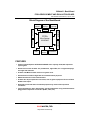
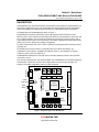
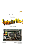
CWdeb01 - BasicBoard FPGA DEVELOPMENT AND EVALUATION BOARD PRELIMINARY USER MANUAL, April 13, 2004 BasicBoard FPGA Development and Evaluation Board User Manual Copyright 2004, Coreworks, Lda 1 coreworks, lda http://www.coreworks.pt CWdeb01 - BasicBoard FPGA DEVELOPMENT AND EVALUATION BOARD PRELIMINARY USER MANUAL, April 13, 2004 TABLE OF CONTENTS FEATURES.................................................................................................................................... 3 DESCRIPTION .............................................................................................................................. 4 POWER SUPPLY .......................................................................................................................... 5 JUMPER SETTINGS ..................................................................................................................... 5 FPGA CONFIGURATION.............................................................................................................. 5 BASICBOARD COMPONENTS .................................................................................................... 6 OSCILLATOR............................................................................................................................. 6 LEDS .......................................................................................................................................... 6 SEVEN-SEGMENT DISPLAYS ................................................................................................. 6 SLIDE SWITCHES ..................................................................................................................... 7 PUSHBUTTONS ........................................................................................................................ 7 RS-232 PORT ............................................................................................................................ 8 PARALLEL PORT ...................................................................................................................... 8 EXPANSION CONNECTORS.................................................................................................... 9 Copyright 2004, Coreworks, Lda 2 coreworks, lda http://www.coreworks.pt CWdeb01 - BasicBoard FPGA DEVELOPMENT AND EVALUATION BOARD PRELIMINARY USER MANUAL, April 13, 2004 Block Diagram of the BasicBoard 55 MHz oscillator 7-segment displays PROM (optional) Expansion connector C FPGA Parallel port Xilinx Spartan XC2S300E LEDs Slide switches Expansion connector D RS-232 port Latches Pushbuttons FEATURES Features a Xilinx Spartan-IIE FPGA XC2S300E with a capacity of 300,000 equivalent system gates. Resources for basic lab work: five pushbuttons, eight LEDs, four 7-segment displays, and eight slide switches. Includes a 55 MHz oscillator useful as a system clock. Parallel Port for FPGA configuration and communication purposes. RS-232 interface for serial communication. Includes two 40-pin expansion connectors, with 74 general-purpose I/Os and 3 FPGA Global Clock Inputs. Designed to mate with other Coreworks peripheral by means of the expansion connectors. Typical applications: basic lab teaching, specific applications using dedicated boards plugged to the expansion connectors (audio, video, etc). Copyright 2004, Coreworks, Lda 3 coreworks, lda http://www.coreworks.pt CWdeb01 - BasicBoard FPGA DEVELOPMENT AND EVALUATION BOARD PRELIMINARY USER MANUAL, April 13, 2004 DESCRIPTION The BasicBoard is an FPGA development and evaluation board suitable for implementation of a wide range of application circuits. The board features a Xilinx Spartan-IIE FPGA (XC2S300E) which has a capacity for implementing circuits with up to 300K system gates of complexity. A simplified layout of the BasicBoard is shown in Figure 1. The BasicBoard provides an assortment of the most frequently used interfaces for basic laboratory work. These interfaces include eight slide switches, five pushbuttons, eight LEDs and four 7-segment displays. There are also two independent expansion connectors with a total of 74 general purpose I/O pins connected directly to the FPGA, 3 Global Clock inputs (GCK) and 3 power pins (3.3 VDC, Ground and Voltage Unregulated). For basic communication with a PC or other equipment, the board includes an RS-232 port and a parallel port. The parallel port is used to send the configuration file to the FPGA. Alternatively, the configuration can be stored in a PROM and loaded at power-up. The PROM is an optional component and a socket is provided for it. The BasicBoard is designed to mate with other Coreworks boards by means of the expansion connectors C and D. This document describes the main blocks available in the BasicBoard. All input/output interfaces are described, in particular, as well as the mapping between the FPGA pins and each I/O interface. The FPGA configuration options are also described. DISP3 DISP2 Latches Latches Power LED Power Switch Xilinx XC2S300E PROM OSC M2 M1 M0 Parallel Port Header Latches FPGA LED8 LED7 LED6 LED5 LED4 LED3 LED2 LED1 Jumpers Parallel Port Latches Expansion Connector C RS-232 Header LEDs 6 V DC Power Jack DISP1 SW1 SW2 SW3 SW4 SW5 SW6 SW7 SW8 Slide Switches Expansion Connector D RS-232 Port DISP4 SW9 Pushbuttons COMM CONF PB1 PB2 PB3 PB4 PB5 Figure 1: Simplified layout of the BasicBoard. Copyright 2004, Coreworks, Lda 4 coreworks, lda http://www.coreworks.pt CWdeb01 - BasicBoard FPGA DEVELOPMENT AND EVALUATION BOARD PRELIMINARY USER MANUAL, April 13, 2004 POWER SUPPLY The BasicBoard uses a 6V DC power supply. The power supply should have a 2.1 mm female, center-positive plug and be capable of delivering at least 500 mA. The board can be switch on and off using the power switch next to the power jack. The board is properly powered when the Power LED is turned on. JUMPER SETTINGS The jumpers select the FPGA configuration mode. Please see the next section (“FPGA Configuration”) for further details. By default the jumpers M0, M1 and M2 are not placed. FPGA CONFIGURATION The FPGA configuration can be loaded from a PC parallel port or from a PROM (not included in the kit). Typically the FPGA configuration is loaded from a PC. In this situation, the parallel port should be used. The signals required by the JTAG programming mode pass throughout this port. To support the JTAG mode, additional circuitry is included in the BasicBoard. In order to prevent a communication failure between the PC and the FGPA, the power supply must be turned on before attaching the parallel cable. To load the configuration from a host computer, follow these steps: 1. apply power to the board, 2. attach the parallel cable (included in the kit) between the PC and the parallel port connector of the BasicBoard, 3. set the slide switch SW9 to the CONF position, 4. remove all jumpers (M0, M1 and M2), 5. run the appropriate configuration software in the PC (e.g., IMPACT from Xilinx). To configure the FPGA from a PROM, follow these steps: 1. place the programmed PROM into the 8-pin socket labeled PROM, 2. set the slide switch SW9 to the COMM position, 3. add all jumpers (M0, M1 and M2), 4. power-on the board. Copyright 2004, Coreworks, Lda 5 coreworks, lda http://www.coreworks.pt CWdeb01 - BasicBoard FPGA DEVELOPMENT AND EVALUATION BOARD PRELIMINARY USER MANUAL, April 13, 2004 BASICBOARD COMPONENTS The BasicBoard provides the following resources: one 55 MHz crystal oscillator eight leds; four 7-segment displays; eight slide switches; five pushbuttons; one RS-232 port; one Parallel port; two 40-pin expansion connectors. These resources are shown in the simplified layout of the BasicBoard (Figure 1), and are described in the following sections. OSCILLATOR The BasicBoard is shipped with a 55 MHz oscillator, whose output is connected to the FPGA GCK0 input (pin 80). The oscillator module is assembled in an 8-pin socket labeled OSC. When a different frequency is required, this oscillator can be replaced by any compatible device. LEDS The BasicBoard provides eight individual LEDs. All of these LEDs are active-high. Table 1 shows the FPGA pins connected to the LEDs. LED LED1 LED2 LED3 LED4 LED5 LED6 LED7 LED8 FPGA pin 40 36 35 34 33 31 30 29 Table 1: FPGA pins for the LEDs. SEVEN-SEGMENT DISPLAYS The BasicBoard provides four seven-segment displays. Each seven-segment display is driven by external D-type latches. The latches are grouped in arrays of 8 latches (one array for each seven-segment display). Each array is addressed by an enable signal provided by the FPGA (see Table 2). The latch is writable when the enable signal is pulled high. Copyright 2004, Coreworks, Lda 6 coreworks, lda http://www.coreworks.pt CWdeb01 - BasicBoard FPGA DEVELOPMENT AND EVALUATION BOARD PRELIMINARY USER MANUAL, April 13, 2004 Display DISP1 DISP2 DISP3 DISP4 FPGA pin 176 178 179 180 Table 2: FPGA pins for the latch enable signal of each display. Each segment in each enabled display is controlled by an FPGA output. The segment turns on, when the FPGA output is pulled to ground (active-low signal). Table 3 shows the FPGA pins for driving the latches of each segment. Segment A B C D E F G Point FPGA pin 194 193 192 191 189 188 187 181 Table 3: FPGA pins for the segment drivers (latches). SLIDE SWITCHES The BasicBoard contains an array of eight slide switches. When closed or ON, each slide switch pulls the FPGA pin to ground. When the slide switch is open or OFF, the pin is pulled high. Table 4 shows the mapping between the FPGA pins and each slide switch. Slide switch SW1 SW2 SW3 SW4 SW5 SW6 SW7 SW8 FPGA pin 49 55 56 57 58 59 60 61 Table 4: FPGA pins for the slide switches. PUSHBUTTONS The BasicBoard has five pushbuttons. When pressed, each pushbutton pulls the FPGA pin to VDD. Otherwise, the pin is pulled to ground through a resistor. The connections between the FPGA and the pushbuttons are presented in Table 5. Copyright 2004, Coreworks, Lda 7 coreworks, lda http://www.coreworks.pt CWdeb01 - BasicBoard FPGA DEVELOPMENT AND EVALUATION BOARD PRELIMINARY USER MANUAL, April 13, 2004 Pushbutton PB1 PB2 PB3 PB4 PB5 FPGA pin 62 63 64 68 69 Table 5: FPGA pins for the pushbuttons. RS-232 PORT The BasicBoard has a 9-pin RS-232 port that provides an interface to transmit and receive serial data streams (TXD and RXD, respectively), as well as the flow control signals (RTS, CTS and DSR). The pin functions on the BasicBoard RS-232 port are identical to those found on a PC serial port. When the BasicBoard and the PC are to communicate, a DTE-to-DCE cable (straight-thru cable) should be used. Table 6 shows the mapping between the FPGA pins and the RS-232 interface. The RS-232 pinout is shown in Figure 2. RS-232 signal RS-232 pin RXD 3 TXD 2 DSR 6 RTS 7 CTS 8 FPGA pin 202 201 200 198 199 Direction I O O I O RS-232 Function Receive Data Transmit Data Data Set Ready Request to Send Clear to Send Table 6: FPGA pins for the RS-232 port. 5 4 9 3 8 2 7 1 6 Figure 2: RS-232 connector (front view). PARALLEL PORT The BasicBoard contains a parallel port connector (25-pins female connector). This interface establishes a communication channel between a computer and the FPGA. The BasicBoard supports both SPP (Simple Parallel Port) and EPP (Enhanced Parallel Port – IEEE 1284) protocols. The EPP protocol is highly recommended because provides a bidirectional data channel and a much higher data transfer rate (see Table 7). NOTE: The parallel port must be configured to the selected protocol (SPP or EPP). In a PC, the parallel port protocol is changed in the BIOS setup. To enter the BIOS setup, the appropriate key (F2, DEL, etc.) must be pressed while the system is starting up. Port Mode SPP EPP Maximum Transfer Rate (MB/s) 0.15 2 Direction Unidirectional (PC ⇒ BasicBoard) Bidirectional Table 7: Comparison between SPP and EPP modes. Copyright 2004, Coreworks, Lda 8 coreworks, lda http://www.coreworks.pt CWdeb01 - BasicBoard FPGA DEVELOPMENT AND EVALUATION BOARD PRELIMINARY USER MANUAL, April 13, 2004 The FPGA configuration can be loaded using the parallel port interface. The slide switch SW9 toggles between the configuration mode (CONF position) and the normal communication (COMM position). Table 8 shows the mapping between the FPGA pins and the parallel port interface. The parallel port pinout is shown in Figure 3. Signal name PWE PD0 PD1 PD2 PD3 PD4 PD5 PD6 PD7 PINT PWT − − PDS − PRS PAS − Connector pin 1 2 3 4 5 6 7 8 9 10 11 12 13 14 15 16 17 18-25 FPGA pin Direction EPP Function 206 15 11 10 9 8 7 6 5 4 3 − − 205 − 203 204 − O I/O I/O I/O I/O I/O I/O I/O I/O I I − − O − O O − Write Enable Address/Data 1 Address/Data 2 Address/Data 3 Address/Data 4 Address/Data 5 Address/Data 6 Address/Data 7 Address/Data 8 Interrupt Wait not connected not connected Data Strobe not connected Reset Address Strobe Ground Table 8: FPGA pins for the parallel port (EPP Mode). 13 12 11 10 9 25 24 23 22 21 8 7 6 5 4 3 2 1 20 19 18 17 16 17 15 14 Figure 3: Parallel port (front view). EXPANSION CONNECTORS Expansion boards with specialized circuitry can be connected to the BasicBoard through expansion connectors C and D. The connector pins have a pitch (spacing) of 100 mils (or 2.54 mm). The ground (GND) is available on pin 1 of connector C (C01), the VDD (3.3 V) is routed to pin C03, and pin C02 provides a Voltage Unregulated (VU) signal (direct connection to the voltage provided by the 6 V DC power jack). All other pins in connectors C and D are routed directly to the FPGA. Among those pins, three of them are connected to dedicated FPGA clock pins. These inputs are available in pins C05, C19 and C29 (connector C). Table 9 shows the mapping between the FPGA pins and the expansion connectors C and D. Copyright 2004, Coreworks, Lda 9 coreworks, lda http://www.coreworks.pt CWdeb01 - BasicBoard FPGA DEVELOPMENT AND EVALUATION BOARD PRELIMINARY USER MANUAL, April 13, 2004 Most of the pins available in the expansion connectors can be used as general-purpose pins (see Table 9). However, some pins can be used to access specific resources in the FPGA (Digital Looked Loops (DLLs), Threshold Reference Voltages, etc.). For further information on the Spartan XC2S300E pinout, please see the datasheets available at the Xilinx website (www.xilinx.com). Copyright 2004, Coreworks, Lda 10 coreworks, lda http://www.coreworks.pt CWdeb01 - BasicBoard FPGA DEVELOPMENT AND EVALUATION BOARD PRELIMINARY USER MANUAL, April 13, 2004 Pin C01 C02 C03 C04 C05 C06 C07 C08 C09 C10 C11 C12 C13 C14 C15 C16 C17 C18 C19 C20 C21 C22 C23 C24 C25 C26 C27 C28 C29 C30 C31 C32 C33 C34 C35 C36 C37 C38 C39 C40 Connector C Name FPGA pin GND − VU − VDD 3.3 V − 16 GCK3 Input 185 17 175 174 173 169 168 167 166 165 164 163 162 20 GCK2 Input 182 154 152 151 150 149 148 147 146 21 GCK1 Input 77 140 139 138 136 22 134 133 132 129 127 43 Direction O O O I/O I I/O I/O I/O I/O I/O I/O I/O I/O I/O I/O I/O I/O I/O I I/O I/O I/O I/O I/O I/O I/O I/O I/O I I/O I/O I/O I/O I/O I/O I/O I/O I/O I/O I/O Pin D01 D02 D03 D04 D05 D06 D07 D08 D09 D10 D11 D12 D13 D14 D15 D16 D17 D18 D19 D20 D21 D22 D23 D24 D25 D26 D27 D28 D29 D30 D31 D32 D33 D34 D35 D36 D37 D38 D39 D40 Connector D Name FPGA pin 45 44 46 125 122 123 47 121 115 23 113 114 111 112 109 110 102 48 100 101 98 99 96 97 94 95 89 93 87 88 84 86 82 83 75 81 73 74 70 71 Direction I/O I/O I/O I/O I/O I/O I/O I/O I/O I/O I/O I/O I/O I/O I/O I/O I/O I/O I/O I/O I/O I/O I/O I/O I/O I/O I/O I/O I/O I/O I/O I/O I/O I/O I/O I/O I/O I/O I/O I/O Table 9: FPGA pins for the expansion connectors C and D. Copyright 2004, Coreworks, Lda 11 coreworks, lda http://www.coreworks.pt