1
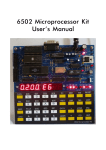
Example Programs for 6502 Microprocessor Kit
0001
0000
0002
0000
GPIO1
0003
0000
0004
0000
0005
0200
0006
0200
0007
0200 A5 00
0008
0202 8D 00 80
0009
0205 00
0010
0206
0011
0206
0012
0206
tasm: Number of errors = 0
.EQU $8000
.ORG $200
LDA $0
STA $GPIO1
BRK
.END
Build Your Own 6502 Microprocessor kit
www.kmitl.ac.th/~kswichit/6502/6502.html
Preface
The example programs for 6502 Microprocessor kit demonstrate
how to enter the computer program in hex code and how to use
the onboard input/output devices, e.g. GPIO1 LED, key switch,
speaker, 7-segment display, and 10ms system tick generator.
Each program is simple and short. The instruction hex codes are
provided. Students can enter the hex code to memory and test it
directly. No need others tools.
The monitor program provides single step running with user
registers and zero page memory displaying. Students can check
the result of CPU operation with these registers easily.
The program can be modified at the 8-bit constants, or even with
the instruction itself, student will learn the result after program
modifications.
For the hardware programming, e.g. key switch, speaker, 7segment display and interrupt please study the hardware
schematic in user manual.
Wichit Sirichote
Contents
Program1: Binary number counting....................4
Program2: Bit shifting.............................................7
Program3: LOAD and STORE...............................8
Program4: 8-bit Addition.......................................9
Program5: Conditional branch instruction.......12
Program6: Reading switch status......................14
Program7: Producing tone 800Hz.....................16
Program8: Simple MORSE code keyer.............18
Program9: Seven segment display....................20
Program10: Testing IRQ with 10ms Tick..........24
Program1: Binary number counting
This program uses memory location 0 in zero page as the 8-bit
variable. We will see the 8-bit binary number counting by writing
the contents of memory location 0 to the GPIO1 LED at location
$8000. Logic 1 will make LED ON and logic 0 for LED OFF.
We can enter the instruction hex code to the memory started
from location $200 to the last byte at location $20D.
To test the program, press key RESET, PC then press STEP and REP
together.
Did you see the 8-bit binary number counting?
Line
0001
0002
0003
0004
0005
0006
Addr hex code
0000
0000
0000
0000
0200
0200
Label
Instruction
GPIO1
.EQU $8000
.ORG 200H
5
0007
0200 A9 00
0008
0202 85 00
0009
0204
0010
0204 A5 00
LOOP
0011
0206 8D 00 80
0012
0209 E6 00
0013
020B
0014
020B 4C 04 02
0015
020E
0016
020E
tasm: Number of errors = 0
LDA #0
STA $0
LDA $0
STA GPIO1
INC $0
JMP LOOP
.END
The 6502 kit display and keypad use hex number. Since each hex
digit represents 4-bit binary number or one nibble. It will make us
more easy to enter the program using hex number.
The actual code in memory is binary number. For example the hex
code of instruction LDA #0 has two bytes A9 and 00. The display
will show us as A9 at location 0200. The real value, however in
memory will be 1010 1001.
Here is the number representation for decimal, binary and
hexadecimal number.
Decimal
0
1
2
3
4
5
6
7
8
4-bit Binary
0000
0001
0010
0011
0100
0101
0110
0111
1000
Hex
0
1
2
3
4
5
6
7
8
9
10
11
12
13
14
15
1001
1010
1011
1100
1101
1110
1111
9
A
B
C
D
E
F
For example the instruction hex code of LDA #0 is A9 and 00.
We can write the first byte in 8-bit binary as 1010 1001 and the
second byte as 0000 0000.
Note
Writing hex number in the Assembly Program can be done with $
or H symbol.
We see that the assembler directive .org 200H will be the same
as .org $200.
The sharp symbol # indicating the number is 8-bit data to be
loaded. If no # symbol, the 8-bit data will be memory location.
For example,
LDA #0 ; load accumulator with data 0
LDA $0 ; load accumulator with memory location 0 in
zero page.
7
Program2: Bit shifting
This program looks similar to Program1, but we use instruction
that shifts the bit, ASL $0, instead of INC $0. Enter the hex code,
then test it with STEP & REP key.
What is the result on the GPIO1 LED?
0001
0000
0002
0000
GPIO1
0003
0000
0004
0000
0005
0200
0006
0200
0007
0200 A9 01
0008
0202 85 00
0009
0204
0010
0204 A5 00
LOOP
0011
0206 8D 00 80
0012
0209 06 00
0013
020B
0014
020B 4C 04 02
0015
020E
0016
020E
tasm: Number of errors = 0
.EQU $8000
.ORG 200H
LDA #1
STA $0
LDA $0
STA GPIO1
ASL $0
JMP LOOP
.END
We see that the GPIO1 LED is very useful for reading the 8-bit
data. We can see the result of internal operation by using the
Accumulator register as the data carrier.
The instruction STA GPIO1, having hex code as 8D 00 80 will
write the contents of accumulator register to GPIO1 LED.
8
Program3: LOAD and STORE
Another method to test program running is to use BRK instruction.
We will test the code with key GO.
Our program has only three instructions, LDA $0, STA $GPIO1
and BRK.
BRK instruction will make the CPU to jump back to monitor
program, saving the CPU registers to user registers. We can keep
the results in user registers for program checking.
This program will load the accumulator with contents at memory
location $0 then write it to GPIO1 LED and ended with BRK
instruction.
0001
0000
0002
0000
GPIO1
0003
0000
0004
0000
0005
0200
0006
0200
0007
0200 A5 00
0008
0202 8D 00 80
0009
0205 00
0010
0206
0011
0206
0012
0206
tasm: Number of errors = 0
.EQU $8000
.ORG 200H
LDA $0
STA $GPIO1
BRK
.END
Enter the hex code, press RESET, PC and GO.
What is result on the GPIO1 LED?
If we change the byte at location $201 from 00 to 01, what is the
result?
9
Program4: 8-bit Addition
Let us play with 8-bit binary addition.
Suppose we want to add two 8-bit binary numbers as shown
below.
Number 1
Number 2
Result is
0101 1011+
0101 1010
__________
5B+
5A
_____
Remember 1+1= 10
Try with hand compute, write the result for both binary and hex.
Now let us check the result from 6502 computing.
0001
0000
0002
0000
GPIO1
.EQU $8000
0003
0000
0004
0000
0005
0200
.ORG 200H
0006
0200
0007
0200 18
CLC
0008
0201 A9 5B
LDA #%01011011
0009
0203 69 5A
ADC #%01011010
0010
0205 8D 00 80
STA $GPIO1
0011
0208 00
BRK
0012
0209
0013
0209
0014
0209
.END
tasm: Number of errors = 0
The program will load number1, 5B to the accumulator. Then add
it with 5B and then write the result to GPIO1 LED.
Do you have got the same result?
10
Since the ADC instruction will add two numbers with carry flag,
so for the rightmost digit, there is no carry flag. We then clear it
beforehand with instruction CLC, CLear Carry.
You can try replace the first byte from 18 (CLC) to 38, SEC
instruction that sets carry flag. And test the program again.
What is the result?
Carry flag will be used for multi ple bytes addition the same as we
add multi ple digits of decimal number.
We can modify above program for testing with logical instructions
as well. By replacing ADC instruction with,
Logical OR with instruction ORA #n
Logical AND,
AND #n
Exclusive OR,
EOR #n
For example if we want to find the result of logical AND between
$4A and $33 the program will be,
0005
0200
.ORG 200H
0006
0200
0007
0200 18
CLC
0008
0201 A9 4A
LDA #$4A
0009
0203 29 33
AND #$33
0010
0205 8D 00 80
STA $GPIO1
0011
0208 00
BRK
0012
0209
0013
0209
0014
0209
.END
tasm: Number of errors = 0
We see that at the address 0203, now the hex code is 29, the
AND instruction. And the 2nd byte is 33, the 8-bit data to be
ANDed with 4A. Result will show on the GPIO1 LED directly.
Note
Symbol % shown in the program is for binary number constant.
Remember $ is for hex number.
The hex code for AND #n is $29
ORA #n is $09
EOR #n is $49
Find more the 6502 hex code from
http://www.obelisk.demon.co.uk/6502/reference.html
Program5: Conditional branch instruction
The 6502 CPU has the instructions that jump with flag condition.
The example of flag is ZERO flag. The zero flag will be '1' when
all bits in a given memory location or register are zero.
We can use such indication for changing program flowing
direction.
Let us see the example of using BNE instruction.
0001
0000
0002
0000
GPIO1
0003
0000
0004
0000
0005
0200
0006
0200
0007
0200 A2 10
0008
0202
0009
0202 8E 00 80
LOOP
0010
0205 CA
0011
0206 D0 FA
0012
0208
0013
0208 8E 00 80
0014
020B 4C 0B 02
HERE
0015
020E
0016
020E
tasm: Number of errors = 0
.EQU $8000
.ORG 200H
LDX #$10
STX GPIO1
DEX
BNE LOOP
STX GPIO1
JMP HERE
.END
Register X is loaded with $10. Main loop is to write the X register
to GPIO1 LED. DEX instruction will decrement X register by one.
Zero flag will be set if the all bits in X register are zero.
We can control the number of loop running by BNE instruction
then.
13
BNE, Branch if Not Equal to ZERO, has two bytes hex code, i.e.
D0 and FA. The second byte, FA is signed number. It is the OFFSET
byte that will be used to add to the current program counter if
the result is not equal to zero.
Current program counter after these two bytes were read by the
CPU is 208. We see from the program that the loop location is
202. Thus the OFFSET byte is 202-208=-6. Or jump backward 6
bytes. We can make -6 from +6 by using 2's complement.
The computer uses 2's complement to represent the negative
number.
Here is +6 in 8-bit binary,
0000 0110
2's complement is 1's complement +1
This is 1's complement
1111 1001
Then +1
1111 1010 or FA, we see that the OFFSET byte FA is then -6.
We can also use key REL for finding the OFFSET byte. At the
display 0206 with D0, press REL key, the address 0206 will be
start address. Press key + for the destination, enter 0202, the
press key GO. The OFFSET byte FA will be placed at address 0207
automatically. On the hex keypad, you may count backward from
key F to key A. You will get -6 is FA!
We will use conditional jump instructions with relative addressing
for many programs.
14
Program6: Reading switch status
The kit has one bit that ties REP switch (S19). We can read the
status of this switch easily by reading it then write it to GPIO1
LED. Logic '1' means switch is opened, and logic '0' means switch
is closed. U13 is tri-state buffer used as the 8-bit input port.
Program is repeating loop read the byte from PORT0. REP key is
tied to bit 6 (PA6). We want to check status only this bit, so we
remove the rest bits with instruction AND #%01000000. Also we
invert it with EOR (Exclusive OR) EOR #%01000000.
0001
0002
0003
0004
0005
0006
0007
0008
0009
0010
0011
0012
0000
0000
0000
0000
0200
0200
0200
0203
0205
0207
020A
020D
GPIO1
PORT0
.EQU 8000H
.EQU 8001H
.ORG 200H
AD
29
49
8D
4C
01 80
40
40
00 80
00 02
LOOP
LDA
AND
EOR
STA
JMP
$PORT0
#%01000000
#%01000000
$GPIO1
LOOP
15
0013
020D
0014
020D
tasm: Number of errors = 0
.END
We test this program with key GO.
What happen if we press key REP?
Note
Logical AND can be used to maskout undesired bit by logic '0'.
Logical Exclusive OR can be used to invert the logic by using logic
'1'.
Logical OR can be used to set the desired bit to be '1' by using
logic '1'.
Program7: Producing tone 800Hz
We can produce the tone signal 800Hz using one bit output port.
A simple tone signal is square wave, ON and OFF. We will try
with 800Hz.
The small speaker is tied to bit 7 of PORT1. It is driven by Q1, PNP
transistor. We can make this bit ON and OFF by writing bit 1 and
bit 0 to this port. Each time we make such bit ON or OFF, a small
delay is inserted. The example shown below, the delay will make
period for ½0.5*1/800Hz.
17
0001
0000
0002
0000
GPIO1
0003
0000
PORT0
0004
0000
PORT1
0005
0000
0006
0200
0007
0200
0008
0200 A9 3F
TONE
0009
0202 8D 02 80
0010
0205 20 13 02
0011
0208 A9 BF
0012
020A 8D 02 80
0013
020D 20 13 02
0014
0210 4C 00 02
0015
0213
0016
0213 A0 79
DELAY
0017
0215 88
DELAY2
0018
0216 D0 FD
0019
0218 60
0020
0219
0021
0219
tasm: Number of errors = 0
.EQU 8000H
.EQU 8001H
.EQU 8002H
.ORG 200H
LDA
STA
JSR
LDA
STA
JSR
JMP
#%00111111
PORT1
DELAY
#%10111111
PORT1
DELAY
TONE
LDY #$79
DEY
BNE DELAY2
RTS
.END
For 800Hz, the half period is 625 microseconds.
The delay subroutine will need to delay approx. a bit smaller than
625 microseconds.
Can you change the frequency? Where is the byte to be modified?
18
Program8: Simple MORSE code keyer
Let us have some fun with MORSE keyer program. We will
combine Program 7 and Program 8. Program 7 enables us to read
status of key REP and Program 8 produces 800Hz tone at the
speaker.
We will read if key REP was pressed, Tone 800Hz will be turned
on. If key REP was released, Tone 800Hz will be turned off.
This will make a simple MORSE code keyer.
0001
0002
0003
0004
0005
0006
0007
0008
0009
0010
0011
0012
0013
0014
0015
0016
0017
0000
0000
0000
0000
0000
0200
0200
0200
0203
0206
0208
020A
020A
020D
020D
0210
0212
GPIO1
PORT0
PORT1
.EQU 8000H
.EQU 8001H
.EQU 8002H
.ORG 200H
20
AD
29
F0
1A 02
01 80
40
F6
MORSE
20 2B 02
AD 01 80
29 40
D0 F9
JSR
LDA
AND
BEQ
TONE
PORT0
#%01000000
MORSE
JSR DELAY
WAIT
LDA PORT0
AND #%01000000
BNE WAIT
19
0018
0214
0019
0214 20 2B 02
0020
0217 4C 00 02
0021
021A
0022
021A A9 3F
TONE
0023
021C 8D 02 80
0024
021F 20 2B 02
0025
0222 A9 BF
0026
0224 8D 02 80
0027
0227 20 2B 02
0028
022A 60
0029
022B
0030
022B A0 79
DELAY
0031
022D 88
DELAY2
0032
022E D0 FD
0033
0230 60
0034
0231
0035
0231
tasm: Number of errors = 0
JSR DELAY
JMP MORSE
LDA
STA
JSR
LDA
STA
JSR
RTS
#%00111111
PORT1
DELAY
#%10111111
PORT1
DELAY
LDY #$79
DEY
BNE DELAY2
RTS
.END
We see that now we have two subroutines, TONE and DELAY.
The TONE subroutine will be called from the main code only when
REP key was pressed.
Testing key status now can be done by using logical AND bit6 of
the PORT0.
MORSE tone is widely used between 750Hz to 900Hz.
Can you modify our code that produces 800Hz for higher or
lower frequency?
20
Program9: Seven segment display
One of the generic device for displaying decimal number is 7segment display. We have the rightmost digit for experimenting by
using jumper J2.
A
F
G
B
C
E
D
DP
The segment A,B,C,D,E,F,G and DP are driven by PORT2.
We see that each bit, CMOS output is capable for driving each
segment of the LED. Logic '1' will make the segment ON.
21
To display a number says, 0,1,2,3,4,5,6,7,8,9, we must convert
the 8-bit value into the corresponding pattern. See the table
below.
Number
0
1
2
3
4
5
6
7
8
9
SEGMENT CODE
$BD
$30
$9B
$BA
$36
$AE
$AF
$38
$BF
$BE
Display
'0'
'1'
'2'
'3'
'4'
'5'
'6'
'7'
'8'
'9'
If we want to show number 0, the segment code $BD will be
used instead. By writing $BD to PORT2 at location $8003 and put
the jumper J2 to pin 1-2.
Our segment driver using 74HC573, CMOS Latch, has no current
limiting resistors. To produce the suitable brightness of the 7segment display, we use PWM (Pulse Width Modulation) method.
The method is to turn ON and OFF the LED at high repetition rate.
To make low brightness, turn ON period will be smaller than turn
OFF period.
The average DC power will then smaller and no heat dissi pation!
If we use series current limiting resistors, heat will be I 2R.
Let us have a look our program.
0001
0000
PORT1
.EQU 8002H
0002
0000
PORT2
.EQU 8003H
0003
0000
0004
0200
.ORG 200H
0005
0200
0006
0200 A9 BF
LDA #$BF
0007
0202 8D 02 80
STA PORT1
0008
0205
0009
0205 A9 BD
LOOP
LDA #$BD
0010
0207 8D 03 80
STA PORT2
0011
020A 20 18 02
JSR DELAYON
0012
020D A9 00
LDA #%00000000
0013
020F 8D 03 80
STA PORT2
0014
0212 20 1E 02
JSR DELAYOFF
0015
0215 4C 05 02
JMP LOOP
0016
0218
0017
0218 A0 01
DELAYON LDY #1
0018
021A 88
DELAY2
DEY
0019
021B D0 FD
BNE DELAY2
0020
021D 60
RTS
0021
021E
0022
021E A0 C8
DELAYOFF LDY #200
0023
0220 88
DELAY3
DEY
0024
0221 D0 FD
BNE DELAY3
0025
0223 60
RTS
0026
0224
0027
0224
0028
0224
.END
tasm: Number of errors = 0
Line 6 and 7 will prevent BREAK command. Let us focus at the
main loop. We first write $BD to PORT2 and call delay for LED
ON. Then turn off all bits at PORT2 and call delay for LED OFF.
The ratio between Time ON and OFF can be approx. using the
loop counter in register Y. We see that it is approx. 1:200 or 0.5%.
Try enter the hex code and test it with key GO. Then put the
jumper J2 to pin 1-2. Check the brightness of the LED.
Can you make it more brighter?
Can you change the number to be displayed?
Before reset the board, remove J2 to pin 2-3.
24
Program10: Testing IRQ with 10ms Tick
The onboard 10ms tick generator is produced by the AT89C2051
microcontroller.
The 10ms tick signal is a 100Hz. We will learn how the 6502
responded with this signal. SW1 is the selector between 10ms tick
or IRQ switch SW2.
25
The 6502 reset and interrupt vectors are put at the last page of
64kB memory space.
2106
2107
2108
2109
2110
2111
2112
2113
2114
EF1F
EF1F
EF1F
EF1F
FFFA
FFFA
FFFA 6C C8
FFFC 00 C0
FFFE 6F C8
; VECTOR NMI,RESET AND IRQ
.ORG 0FFFAH
.WORD
.WORD
.WORD
NMI
0C000H
IRQ
; NMI
; RESET
; IRQ
The monitor program put the vector address for IRQ at location
$C86F.
1923
1924
C86C 6C FA 00
C86F 6C FE 00
NMI
IRQ
JMP
JMP
($FA)
($FE)
At the location $C86F, we put JUMP indirect using RAM vector at
location $00FE for low byte and $00FF for high byte.
With this method, we can then test the IRQ process by placing the
IRQ vector in RAM.
0001
0002
0003
0004
0005
0006
0007
0008
0009
0000
0000
0000
0000
0000
0000
0000
0030
0030
GPIO1
PORT0
PORT1
PORT2
.EQU
.EQU
.EQU
.EQU
8000H
8001H
8002H
8003H
.ORG $30
0010
0011
0012
0013
0014
0015
0016
0017
0018
0019
0020
0021
0022
0023
0024
0025
0026
0027
0028
0029
0030
0031
0032
0033
0034
0035
0036
0037
0038
0039
0040
0041
0042
0043
0044
0045
0046
0030
0031
0032
0032
00FE
00FE
0100
0200
0200
0200
0202
0204
0206
0208
0208
0209
020C
020C
020C
020C
020C
020D
020D
020E
0210
0212
0214
0216
0218
021A
021A
021B
021D
021F
0221
0221
0223
SEC100
SEC
.BLOCK 1
.BLOCK 1
.ORG $FE
.WORD SERVICE_IRQ
0C 02
.ORG 200H
A9
85
A9
85
0C
FE
02
FF
58
4C 09 02
MAIN
LDA #SERVICE_IRQ&$FF
STA $FE
LDA #2
STA $FF
CLI
; ENABLE IRQ
JMP $ ; jump here
SERVICE_IRQ
78
SEI
F8
E6
A5
C9
D0
A9
85
SED
INC
LDA
CMP
BNE
LDA
STA
30
30
64
10
00
30
;DECIMAL MODE
SEC100
SEC100
#100
SKIP1
#0
SEC100
18
A5 31
69 01
85 31
CLC
LDA SEC
ADC #1
STA SEC
A5 31
8D 00 80
LDA SEC
STA GPIO1
0047
0226
0048
0226
SKIP1
0049
0226 40
0050
0227
0051
0227
0052
0227
tasm: Number of errors = 0
RTI
.END
Main program begins with storing the service address of IRQ at
location $00FE and $00FF. The service address is $020C. Then
ENABLE the interrupt with instruction CLI. And jump here waiting
the trigger from 10ms tick.
When the CPU recognize the IRQ trigger, it will save current PC
and jump to interrupt service subroutine at $020C.
The service for IRQ will be entered every 10ms. The SEC100
variable will be incremented, when it is 100, it will be one second.
The SEC variable will then be incremented in BCD number and
wrote to the GPIO1 LED.
Let us test the code with key GO and see what happen on the
GPIO1 LED?