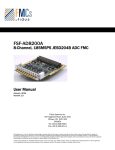
1
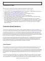
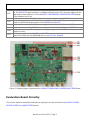
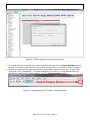
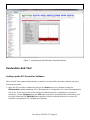
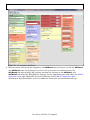
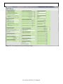
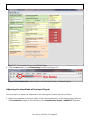
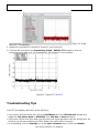
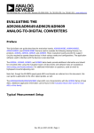
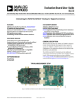
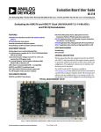
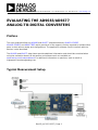
One Technology Way · P.O. Box 9106 · Norwood, MA 02062-9106 · Tel: 781.329.4700 · Fax: 781.461.3113 · www.analog.com
EVALUATING THE AD9683/AD6677
ANALOG-TO-DIGITAL CONVERTERS
Preface
This user guide describes the AD9683 and AD6677 evaluation boards; AD9683-170EBZ,
AD9683-250EBZ, and AD6677EBZ; which provide all of the support circuitry required to operate these
parts in their various modes and configurations. The application software used to interface with the
devices is also described.
The AD9683 and AD6677 data sheets provide additional information and should be consulted when
using the evaluation board. All documents and software tools are available at
www.analog.com/hsadcevalboard. For additional information or questions, send an email to
[email protected].
Typical Measurement Setup
Rev 05 Jun 2013 16:37 | Page 1
Figure 1. Evaluation Board Connection—AD9683-170EBZ, AD9683-250EBZ, or AD6677EBZ (on Left)
and HSC-ADC-EVALDZ (on Right)
Features
●
●
●
●
●
●
Full featured evaluation board for the AD9683/AD6677
SPI interface for setup and control
External, on-board oscillator, or AD9525 clocking option
Balun/transformer or amplifier input drive option
On-board LDO regulator needing a single external 6 V, 2 A dc supply
VisualAnalog® and SPI controller software interfaces
Helpful Documents
●
●
●
●
●
●
AD9683 or AD6677 data sheet
High speed ADC FIFO evaluation kit (HSC-ADC-EVALCZ)
AN-905 Application Note, VisualAnalogTM Converter Evaluation Tool Version 1.0 User Manual
AN-878 Application Note, High Speed ADC SPI Control Software
AN-877 Application Note, Interfacing to High Speed ADCs via SPI
AN-835 Application Note, Understanding High Speed ADC Testing and Evaluation
Equipment Needed
●
●
●
●
●
●
●
●
Analog signal source and antialiasing filter
Sample clock source (if not using the on-board oscillator)
(1) 6.0 V, 2.5 A switching power supply, CUI EPS060250UH-PHP-SZ provided
(1) 12.0V, 3.3 A switching power supply, V-Infinity ETSA120330UDC-PFP-SZ provided
PC running Windows®
USB 2.0 port
AD9683-170EBZ, AD9683-250EBZ, or AD6677EBZ board
HSC-ADC-EVALDZ FPGA-based data capture kit
Getting Started
This section provides quick start procedures for using the AD9683-170EBZ, AD9683-250EBZ, or
AD6677EBZ board. Both the default and optional settings are described.
Rev 05 Jun 2013 16:37 | Page 2
Configuring the Board
Before using the software for testing, configure the evaluation board as follows:
1. Connect the evaluation board to the data capture board, as shown in Figure 1.
2. Connect one 6 V, 2.5 A switching power supply (such as the CUI, Inc., EPS060250UH-PHP-SZ that is
supplied) to the AD9683-170EBZ, AD9683-250EBZ, or AD6677.
3. Connect one 12 V, 3.3 A switching power supply (such as the supplied V-Infinity
ETSA120330UDC-PFP-SZ) to the HSC-ADC-EVALCZ board.
4. Connect the HSC-ADC-EVALDZ board (P702) to the PC using a USB cable.
5. On the ADC evaluation board, confirm that the jumpers are installed at P202, P209, P204, P205,
P206, and P210 as shown in Figure 2 and Table 1.
6. On the ADC evaluation board, use a clean signal generator with low phase noise to provide an
input signal to the AD9683 analog input. Use a 1 m, shielded, RG-58, 50 Ω coaxial cable to connect
the signal generator. For best results, use a narrow-band, band-pass filter with 50 Ω terminations
and an appropriate center frequency. (Analog Devices, Inc., uses TTE, Allen Avionics, and K&L
band-pass filters.)
Evaluation Board Hardware
The evaluation board provides the support circuitry required to operate the AD9683 and AD6677 in
their various modes and configurations. Figure 1 shows the typical bench characterization setup used
to evaluate AC performance. It is critical that the signal sources used for the analog input and clock
have very low phase noise (<1 ps rms jitter) to realize the optimum performance of the signal chain.
Proper filtering of the analog input signal to remove harmonics and lower the integrated or broadband
noise at the input is necessary to achieve the specified noise performance.
See the evaluation board pages linked from the AD9683 and AD6677 product pages for the complete
schematics and bill of materials (BOM). The evaluation board layout is available upon request. The
layout diagrams demonstrate the routing and grounding techniques that should be applied at the
system level when designing application boards using these converters.
Power Supplies
This evaluation board comes with a wall-mountable switching power supply that provides a 6 V, 2 A
maximum output. Connect the supply to a 100 V ac to 240 V ac, 47 Hz to 63 Hz wall outlet. The
output from the supply is provided through a 2.1 mm inner diameter jack that connects to the printed
circuit board (PCB) at P201. The 6 V supply is fused and conditioned on the PCB before connecting to
the low dropout linear regulators that supply the proper bias to each of the various sections on the
board.
The evaluation board can be powered in a nondefault condition using external bench power supplies.
To do this, remove the all the jumpers listed above (and in Table 1) to disconnect the outputs from
the on-board LDOs. This enables the user to bias each section of the board individually. Use P1, P208,
Rev 05 Jun 2013 16:37 | Page 3
and P502 to connect a different supply for each section. A 1.8 V, 0.5 A supply is needed for 1.8
V_AVDD, 1.8 V_DVDD, and 1.8 V_DRVDD. Although the power supply requirements are the same for
AVDD, DVDD, and DRVDD, it is recommended that separate supplies be used for both analog and
digital domains. The DVDD and DRVDD voltages can be driven from the same power supply. The SPI
and its level shifters and alternate clock options require a separate 3.3 V, 0.5 A analog supply. In
addition, if using the AD9525 and/or the ADL5202, a separate 5.0 V, 0.5 A analog supply is required.
Input Signals
When connecting the ADC clock and analog source, use clean signal generators with low phase noise,
such as the Rohde & Schwarz SMA, or HP 8644B signal generators or an equivalent. Use a 1 m
shielded, RG-58, 50 Ω coaxial cable for connecting to the evaluation board. Enter the desired
frequency and amplitude (see the Specifications section in the data sheet of the respective part).
When connecting the analog input source, use of a multipole, narrow-band band-pass filter with 50 Ω
terminations is recommended. Analog Devices uses band-pass filters from TTE and K&L Microwave,
Inc. Connect the filters directly to the evaluation board.
If an external clock source is used, it should also be supplied with a clean signal generator as
previously specified. Analog Devices evaluation boards typically can accept ~2.8 V p-p or 13 dBm sine
wave input for the clock.
Output Signals
The default setup uses the Analog Devices high speed converter evaluation platform (
HSC-ADC-EVALDZ) for data capture. The serial JESD204B outputs from the ADC are routed to
Connector P1002 using 100 Ω differential traces. For more information on the data capture board and
its optional settings, visit www.analog.com/hsadcevalboard.
Jumper Settings
Set the jumper settings/link options on the evaluation board for the required operating modes before
powering on the board. The functions of the jumpers are described in Table 1. Figure 2 shows the
default jumper settings.
Table 1. Jumper Settings
Jumper Description
Rev 05 Jun 2013 16:37 | Page 4
P202
P209
P210
P205
P206
P204
P504
This jumper sets up the 5.0 V power supply voltage for the outputs of the on-board ADL5202.
For the ADL5202 to work properly, its outputs must be tied to a 5.0 V power supply via the
appropriate sized inductors. On the AD9683-170EBZ/AD9683-250EBZ/AD6677EBZ boards
these inductors are 1 uH.
This jumper sets up the 3.3V analog power supply voltage for the ADL5202.
This jumper connects the DVDD power supply domain to the DRVDD power supply domain to
power the JESD204B output drivers of the AD9683 and AD6677.
This jumper connects the AVDD power supply domain of the AD9683 and AD6677.
This jumper connects the DVDD power supply domain of the AD9683 and AD6677.
This jumper sets up a 3.3 V digital power supply voltage for the AD9525 and also powers SPI
related circuitry.
This jumper connects the AD9683 and AD6677 external clock input to the reference clock
input of the FPGA (for the JESD204B link) on the HSC-ADC-EVALDZ.
Figure 2. Default Jumper Connections for AD9683-170EBZ/AD9683-250EBZ/AD6677EBZ Board
Evaluation Board Circuitry
This section explains the default and optional settings or modes allowed on the AD9683-170EBZ,
AD9683-250EBZ, and AD96677EBZ boards.
Rev 05 Jun 2013 16:37 | Page 5
Power
Plug the switching power supply into a wall outlet rated at 100 V ac to 240 V ac, 47 Hz to 63 Hz.
Connect the DC output connector to P101 on the evaluation board.
Analog Input
The analog input on the evaluation board is set up for a double balun-coupled analog input with a 50
Ω impedance. The default analog input configuration supports analog input frequencies of up to ~400
MHz. For additional information on recommended input networks, see the AD9683 and AD6677 data
sheets.
Optionally, the AD9683 and AD6677 analog input can be configured to use the ADL5202 digitally
controlled, variable gain wide bandwidth amplifier. The ADL5202 is included on the evaluation board
at U401. The path into and out of the ADL5202 can be configured many different ways depending on
the application; therefore, several of the components in the input and output path are left
unpopulated. See the ADL5202 data sheet for additional information on this part and for configuring
the inputs and outputs.
In order to connect the active path using the ADL5202 a few resistors need to be changed. First,
remove C305 and C306. Then populate R311 and R312. These changes disconnect the passive input
and connect the output of the ADL5202 to the analog inputs of the AD9683 and AD6677. Next, place
the desired filter components at the output of the ADL5202. As mentioned, these are not populated
by default since there are many different possibilities. J404 must also be populated so that the input
of the ADL5202 can be driven with an external signal source.
Clock
Nyquist Clock
The default clock input circuit connects to the Nyquist clock input of the AD9683 and AD6677. The
clock is derived from a simple transformer-coupled circuit using a high bandwidth 1:1 impedance ratio
transformer (T503) that adds a low amount of jitter to the clock path. The clock input is 50 Ω
terminated and ac-coupled to handle single-ended sine wave types of inputs. The transformer
converts the single-ended input to a differential signal before entering the ADC clock inputs. The
AD9683 and AD6677 ADCs are equipped with an internal 8:1 clock divider to facilitate usage with
higher frequency clocks. The clock input for the Nyquist clock is the CLK+ SMA connector.
RF Clock
Rev 05 Jun 2013 16:37 | Page 6
The AD9683 and AD6677 are also equipped with a single-ended RF Clock input that can receive input
frequencies from 625 MHz up to 1.5 GHz. This feature must be enabled via SPI and a clock of
appropriate frequency must be connected to the RF_CLK SMA connector. The RF Clock circuitry within
the AD9683 and AD6677 has a selectable /2 or /4 pre-divider in addition to the internal 8:1 clock
divider to facilitate usage with higher frequency clocks up to 1.5 GHz.
Clocking with the AD9525
The AD9683 and AD6677 boards may also be set up to be clocked from the AD9525.
PDWN
To enable the power-down feature, add a shorting jumper across P3 (directly to the right of P209) at
Pin 1 and Pin 2 to connect the PDWN pin to DRVDD.
RSTB
To enable the reset feature, add a shorting jumper across P101 at Pin 1 and Pin 2 to connect the RSTB
pin to GND.
How To Use The Software For Testing
Setting up the ADC Data Capture
After configuring the board, set up the ADC data capture using the following steps:
1. Open VisualAnalog on the connected PC. The appropriate part type should be listed in the status
bar of the VisualAnalog – New Canvas window. Select the template that corresponds to the type
of testing to be performed (see Figure 3, where the AD9683 is shown as an example).
Rev 05 Jun 2013 16:37 | Page 7
Figure 3. VisualAnalog, New
Canvas Window
2. After the template is selected, a message appears asking if the default configuration can be used
to program the FPGA (see Figure 4). Click Yes, and the window closes.
Figure 4. VisualAnalog Default
Configuration Message
3. Click the Settings button on the ADC Data Capture block. In the pop-up window select the
Capture Board tab. Select the checkbox Poll Full Flag. This must be checked in order to get
data capture from the AD9683 and AD6677 (see Figure 5).
Rev 05 Jun 2013 16:37 | Page 8
Figure 5. VisualAnalog ADC Data Capture Settings
1. To change features to settings other than the default settings, click the Expand Display button,
located in the bottom right corner of the window (see Figure 6), to see what is shown in Figure 7.
2. Change the features and capture settings by consulting the detailed instructions in the AN-905
Application Note, VisualAnalogTM Converter Evaluation Tool Version 1.0 User Manual. After the
changes are made to the capture settings, click the Collapse Display button.
Figure 6. VisualAnalog Window Toolbar, Collapsed Display
Rev 05 Jun 2013 16:37 | Page 9
Figure 7. VisualAnalog, Main Window, Expanded Display
Evaluation And Test
Setting up the SPI Controller Software
After the ADC data capture board setup is complete, set up the SPI controller software using the
following procedure:
1. Open the SPI controller software by going to the Start menu or by double-clicking the
SPIController software desktop icon. If prompted for a configuration file, select the appropriate
one. If not, check the title bar of the window to determine which configuration is loaded. If
necessary, choose Cfg Open from the File menu and select the appropriate file based on your
part type. Note that the CHIP ID(1) box should be filled to indicate whether the correct SPI
controller configuration file is loaded (see Figure 8).
Rev 05 Jun 2013 16:37 | Page 10
Figure 8. SPI Controller, CHIP ID(1) Box
2. Click the New DUT button in the SPIController window (see Figure 9).
Rev 05 Jun 2013 16:37 | Page 11
Figure 9. SPI Controller, New DUT Button
3. In the ADCBase 0 tab of the SPIController window, find the CLOCK DIVIDE(B) box (see Figure
10). If using the clock divider, use the drop-down box to select the correct clock divide ratio, if
necessary. The Nyquist Clock is selected by default. If using the RF Clock, make sure to configure
the device in this tab. For additional information, refer to the data sheet, the AN-878 Application
Note, High Speed ADC SPI Control Software, and the AN-877 Application Note, Interfacing to High
Speed ADCs via SPI.
Rev 05 Jun 2013 16:37 | Page 12
Figure 10. SPI Controller, ADCBase0
4. Note that other settings can be changed on the ADCBase0 tab (see Figure 10) and the ADCBase1
and ADCBase2 tabs (see Figures 11 and 12) to set up the part in the desired mode. The
ADCBase0 tab settings affect ADC settings, whereas the settings on the ADCBase1 and
ADCBase2 tabs affect the JESD204B link settings. See the appropriate part data sheet, the AN-878
Application Note, High Speed ADC SPI Control Software, and the AN-877 Application Note,
Interfacing to High Speed ADCs via SPI, for additional information on the available settings.
Rev 05 Jun 2013 16:37 | Page 13
Figure 11. SPI Controller, Example ADCBase1 Page
Rev 05 Jun 2013 16:37 | Page 14
Figure 12. SPI Controller, Example ADCBase1 Page
5. Click the Run button in the VisualAnalog toolbar (see Figure 13).
Figure 13. Run Button (Encircled in Red) in VisualAnalog Toolbar, Collapsed Display
Adjusting the Amplitude of the Input Signal
The next step is to adjust the amplitude of the input signal for each channel as follows:
1. Adjust the amplitude of the input signal so that the fundamental is at the desired level. Examine
the Fund Power reading in the left panel of the VisualAnalog Graph - AD9253 FFT window
Rev 05 Jun 2013 16:37 | Page 15
(see Figure 14).
Figure 14. Graph
Window of VisualAnalog
2. Repeat this procedure for Channel B, Channel C, and Channel D.
3. Click the disk icon within the VisualAnalog Graph - AD9253 FFT window to save the
performance plot data as a .csv formatted file. See Figure 15 for an example.
Figure 15. Typical FFT, AD9253
Troubleshooting Tips
If the FFT plot appears abnormal, do the following:
●
●
●
If you see an abnormal noise floor, go to the ADCBase0 tab of the SPIController window and
toggle the Chip Power Mode in MODES(8) from Chip Run to Reset and back.
If you see a normal noise floor when you disconnect the signal generator from the analog input, be
sure that you are not overdriving the ADC. Reduce the input level if necessary.
In VisualAnalog, click the Settings icon in the Input Formatter block. Check that Number
Rev 05 Jun 2013 16:37 | Page 16
Format is set to the correct encoding (twos complement by default). Repeat for the other channels.
If the FFT appears normal but the performance is poor, check the following:
●
●
●
●
Make sure that an appropriate filter is used on the analog input.
Make sure that the signal generators for the clock and the analog input are clean (low phase noise).
Change the analog input frequency slightly if noncoherent sampling is being used.
Make sure that the SPI configuration file matches the product being evaluated.
If the FFT window remains blank after Run in VisualAnalog (see Figure 11) is clicked, do the following:
●
●
●
Make sure that the evaluation board is securely connected to the HSC-ADC-EVALDZ board.
Make sure that the FPGA has been programmed by verifying that the DONE LED is illuminated on
the HSC-ADC-EVALDZ board. If this LED is not illuminated, make sure that the U4 switch on the
board is in the correct position for USB CONFIG.
Make sure that the correct FPGA program was installed by clicking the Settings icon in the ADC
Data Capture block in VisualAnalog. Then select the FPGA tab and verify that the proper FPGA bin
file is selected for the part.
If VisualAnalog indicates that the FIFO Capture timed out, do the following:
●
●
Make sure that all power and USB connections are secure.
Make sure that the Poll Full Flag checkbox is checked under ADC Capture Settings in Visual
Analog.
© Analog Devices, Inc. All rights reserved. Trademarks and
registered trademarks are the property of their respective owners.
Rev 05 Jun 2013 16:37 | Page 17
www.analog.com