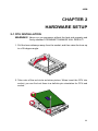
1
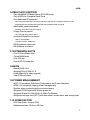
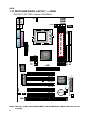
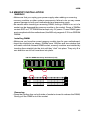
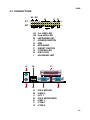
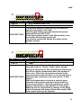
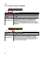
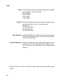
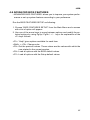
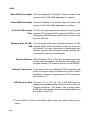
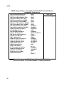
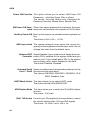
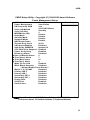
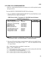
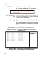
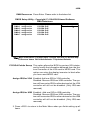
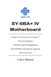
R
SL-65EB V1.0
USER MANUAL
USER NOTICE
T
Product Model
Manual Revision
Release Date
: SL-65EB
: V1.0
: OCTOBER 2000
His Users Guide & Technical Reference is for assisting system
manufacturers and end-users in setting up and installing the
motherboard.
Every effort has been made to ensure that the information in this
manual is accurate. Soltek Computer Inc. is not responsible for printing or clerical errors. Information in this document is subject to
change without notice and does not represent a commitment on the
part of Soltek Computer Inc.
No part of this manual may be reproduced, transmitted, translated
into any language in any form or by any means, electronic or
mechanical, including photocopying and recording, for any purpose
without the express written permission of Soltek Computer Inc.
Companies and products mentioned in this manual are for identification purpose only. Product names appearing in this manual may
or may not be registered trademarks or copyrights of their respective companies.
Soltek computer inc. Provides this manual “As is “ without warranty
of any kind, either express or implied, including but not limited to
the implied warranties or conditions of merchantability or fitness for
a particular purpose. In no event shall Soltek computer inc. Be liable for any loss or profits, loss of business, loss of use or data,
interruption of business, or for indirect, special, incidental, or consequential damages of any kind, even if Soltek computer inc. Has
been advised of the possibility of such damages arising from any
defect or error in this manual or product.
Copyright © 2000 Soltek Computer Inc. All Rights Reserved.
• Intel, Celeron, Pentium II, Pentium III are trademarks of Intel Corporation.
• Intel 82815 Graphic Memory Controller Hub(GMCH), 82801 I/O Controller Hub(ICH) are trademarks of Intel Corporation.
• VIA Cyrix III is trademark of VIA Corporation.
• Norton AntiVirus, Norton Ghost are trademarks of Symantec Corporation.
SOLTEK AROUND THE WORLD
SOLTEK COMPUTER INC.
Address
Telephone
Fax
E-mail
Web site
: 7F, No. 306-3, Ta-Tung Rd, Sec.1, Hsi-Chin, TaipeiHsien, Taiwan, R.O.C.
: 886-2-2642-9060
: 886-2-2642-9065
: [email protected]
: http://www.soltek.com.tw
SOLTEK KOREA INC.
Address
Telephone
Fax
E-mail
: 1002, Chungjin Bldg. 53-5 Wonhyo-Ro, 3-Ka,
Yongsan-Ku Seoul 140-113, Korea
: 82-2-32717400
: 82-2-32717405
: [email protected]
MOKA HOLDING B.V.
Address
Telephone
Fax
E-mail
: De Run 4428 5503 LR Veldhoven, the Netherlands
: 31-402-556150
: 31-402-546006
: [email protected]
SOUL TECHNOLOGY EUROPE B.V.
Address
Telephone
Fax
E-mail
Web site
: Sydneystraat 52-54 3047 BP Rotterdam, the Netherlands
: 31-10-2457492
: 31-10-2457493
: [email protected]
: http://www.soultech-europe.com
65EB
CONTENT
CHAPTER 1
INTRODUCTION .................................................................. 6
1-1 ITEM LIST CHECK UP .............................................................................. 6
1-2 CHIPSET ................................................................................................... 6
1-3 PROCESSOR ............................................................................................ 6
1-4 ADVANCED HIGH-PERFORMANCE DRAM CONTROLLER ................... 6
1-5 FULL FEATURED ACCELERATED GRAPHICS PORT ............................ 6
1-6 MULTI-I/O FUNCTION ............................................................................... 7
1-7 EXTENSION SLOTS ................................................................................. 7
1-8 BIOS .......................................................................................................... 7
1-9 POWER MANAGEMENT ........................................................................... 7
1-10 FORM FACTOR ....................................................................................... 7
1-11 MOTHERBOARD LAYOUT --- 65EB ....................................................... 8
1-12 CHIPSET SYSTEM BLOCK DIAGRAM ................................................... 9
CHAPTER 2
HARDWARE SETUP ......................................................... 11
2-1 CPU INSTALLATION ............................................................................... 11
2-2 MEMORY INSTALLATION ....................................................................... 13
2-3 Hdd / fdd installation ................................................................................ 14
2-4 CPU TYPE CONFIGURATION ................................................................ 15
2-5 SYSTEM MEMORY CONFIGURATION .................................................. 16
2-6 JUMPER DEFINITION ............................................................................. 16
2-6.1 ONBOARD (CFAN1/SFAN1/PFAN1) .................................................... 16
2-6.2 KEYBOARD POWER ON (JP2) ........................................................... 17
2-6.3 USB PORT SELECT (JP6/JP7) ............................................................ 17
2-6.4 POWER LOST RESUME (JP12) .......................................................... 17
2-6.5 VGA CARD (JVGA1) ............................................................................ 18
2-6.6 CLEAR CMOS DATA (JBAT1) .............................................................. 18
2-6.7 WAKE ON LAN (WOL) FUNCTION (JWOL1) ...................................... 18
2-7 CONNECTORS ....................................................................................... 19
2-7.1 J1 SWITCH SIGNAL SUMMARY ......................................................... 20
4
65EB
2-7.2 J2 SWITCH SIGNAL SUMMARY ......................................................... 22
2-7.3 ATX POWER SUPPLY CONNECTOR .................................................. 24
2-7.4 PS/2 MOUSE AND PS/2 KEYBOARD .................................................. 24
2-7.5 IRQ DESCRIPTION .............................................................................. 25
CHAPTER 3
SOFTWARE SETUP .......................................................... 26
3-1 ABOUT THE SUPPORT CD ....................................................... 26
3-2 INTEL CHIPSET DRIVER INSTALLATION (FOR ....................... 26
WINDOWS 95/98/2000) .............................................................. 26
CHAPTER 4
BIOS SETUP ..................................................................... 28
4-1 INTRODUCE THE BIOS .......................................................................... 28
4-2 WHAT IS BIOS SETUP ............................................................................ 28
4-3 HOW TO RUN BIOS SETUP ................................................................... 28
4-4 WHAT IS CMOS ...................................................................................... 29
4-5 WHAT IS POST ....................................................................................... 29
4-6 BIOS UPGRADE ...................................................................................... 29
4-6.1 BEFORE UPGRADE BIOS ................................................................... 29
4-6.2 UPGRADE PROCESS ......................................................................... 30
4-7 CMOS SETUP UTILITY ........................................................................... 33
4-8 STANDARD CMOS FEATURES .............................................................. 34
4-9 ADVANCED BIOS FEATURES ................................................................ 37
4-10 ADVANCED CHIPSET FEATURES ....................................................... 41
4-11 INTEGRATED PERIPHERALS .............................................................. 45
4-12 POWER MANAGEMENT SETUP .......................................................... 50
4-13 PNP / PCI CONFIGURATION ................................................................ 55
4-14 FREQUENCY CONTROL ...................................................................... 58
4-15 LOAD OPTIMIZED DEFAULTS ............................................................. 58
4-16 SET SUPERVISOR / USER PASSWORD ............................................. 60
4-17 SAVE & EXIT SETUP ............................................................................ 61
4-18 EXIT WITHOUT SAVING ....................................................................... 61
5
65EB
CHAPTER 1
INTRODUCTION
1-1 ITEM LIST CHECK UP
• Motherboard
• Support CD
• User’s Manual
• Bundle Bonus Pack CD
• Bundle Bonus Pack Manual
• ATA33 IDE Cable
1-2 CHIPSET
• North Bridge - Intel 82443BX.
• South Bridge - 82371EB PCI-To-ISA.
• Supper I/O - Winbond W83977.
1-3 PROCESSOR
• Supports Intel® FC-PGA Pentium IIITM up to 1GHz (100MHz Front Side
Bus only).
• Supports Intel® FC-PGA 370 Celeron & PGA 370 Celeron up to 700MHz.
• Supports VIA Cyrix III up to 600MHz.
• Supports CPU voltage Auto - Detect circuit.
• Supports CPU using front side Bus 66MHz and 100MHz only.
1-4 ADVANCED HIGH-PERFORMANCE DRAM
CONTROLLER
• Supports SDRAM memory up to 3 DIMMS.
• 64-bit data width and 3.3V DRAM interface.
• Supports up to 768MB memory space.
• Different DRAM types may be used in mixed combinations.
1-5 FULL FEATURED ACCELERATED GRAPHICS PORT
• Supports 66MHz 1x and 2x modes.
• AGP Specification Rev 1.0 compliant.
6
65EB
1-6 MULTI-I/O FUNCTION
• Two UltraDMA-33 Master Mode PCI EIDE ports.
• Two UARTs for Complete Serial Ports.
• One dedicated IR connector:
Third serial port dedicated to IR function either through the two complete serial ports or the
third dedicated port Infrared-IrDA (SIR) and ASK (Amplitude Shift Keyed) IR.
• Multi-mode parallel connector:
Standard mode, ECP and EPP support.
• Floppy Disk connector:
One FDD with drive swap support.
• Universal Serial Bus connector:
USB V1.0 compatible.
Provides 2 build-in USB ports.
• PS/2 Keyboard connector.
• PS/2 Mouse connector.
1-7 EXTENSION SLOTS
• Five PCI bus Mater slots.
• Three DIMM slots.
• One ISA slot.
• One AGP 2X mode slot.
1-8 BIOS
• Award BIOS V6.0.
• Supports Plug & Play V1.0.
• Flash Memory for easy upgrade.
• Year 2000 compliant.
1-9 POWER MANAGEMENT
• ACPI 1.0 compliant (Advanced Configuration and Power Interface).
• APM V1.2 compliant (Legacy power management).
• System event monitoring with two event classes.
• Supports PS/2 Keyboard & Mouse power on.
• Supports Wake On LAN (WOL) & Wake On Modem.
• Supports real time clock (RTC) with date alarm, month alarm, and century field.
1-10 FORM FACTOR
• ATX from factor, 4 layers PCB.
• Motherboard size 18.0cm x 30.5cm.
7
65EB
1-11 MOTHERBOARD LAYOUT --- 65EB
DIMM1
DIMM2
DIMM3
• DEFAULT SETTING: Celeron 300/66MHz.
upper
USB1
lower
USB0
1
82443BX
Host
Bridge
SW1
8 7 6 5 4 3 2 1
SFAN1
JP6 1
JP7 1
FDC
ON
IDE2
DIP
Clock
Generator
PC100/PC133 SDRAM
ATX POWER
COM2
COM1
LPT1
SOCKET 370
CFAN1
3
3
AGP
I/O
Controller
IDE1
upper
PS/2
MOUSE
lower
PS/2
K/B
3
JP2
SUSLED
82371EB
(PIIX4E)
(PCI-to-ISA
Bridge)
PWR/LED
PCI 3
PWR SMI
JVGA1
15
15
PCI 2
3
JP12
PCI 5
SPK
3
HD/LED
JBAT1
Li
Battery
PFAN1 J1
J2
1
1
JWOL1
PCI 4
RST
IR
FLASH BIOS
PCI 1
ISA
NOTE: FOR 100 / 133MHz CPU ENVIRONMENT, THE SDRAM MUST COMPLY WITH PC-100 / PC133 SPEC.
8
65EB
1-12 CHIPSET SYSTEM BLOCK DIAGRAM
Socket 370
CPU
AGP Slot or
3D Graphics
Controller
AGP 2X Slot
82443BX
Host
Bridge
Main
Memory
(DRAM)
PCI5
PCI4
PCI3
PCI2
PCI1
IDE x 2 Ports
(Ultra DMA/33)
USBx2
Super lO
Serial Port x 2
Infrared Port x 1
Parallel Port x 1
FDD x1
82371EB
(PIIX4E)
(PCI-to-ISA
Bridge)
ISA1
BIOS
ROM
Keyboard
& Mouse
Figure 1-11. 82443BX System Block Diagram Using the
82371EB South Bridge
9
65EB
ATTENTION !!!
1. Please refer to your processor installation or other
documentation attached with your CPU for detailed
installing instruction.
2. Installing a heat sink and cooling fan is necessary for
proper heat dissipation from your CPU. Uncorrected
installation may result in overheating and damage of
your CPU.
3. Before changing the setting of CPU Vcore from BIOS
program, user SHOULD make sure of correct specification both of CPU CLOCK and RATIO. Uncorrected
setting may cause damage to your CPU.
10
65EB
CHAPTER 2
HARDWARE SETUP
2-1 CPU INSTALLATION
WARNING ! Never run you processor without the heat sink properly and
firmly attached. PERMANET DAMAGE WILL RESULT!
1. Pull the lever sideways away from the socket, and then raise the lever up
to a 90-degree angle.
T
KE
370
C
SO
2. Take note of the red circle as below picture. When insert the CPU into
socket, you can find out there is a definite pin orientation for CPU and
socket.
70
T3
E
CK
SO
11
65EB
3. Make sure that the CPU positions in the socket tightly, and then put the
lever down to complete the CPU installation.
C
SO
12
70
T3
E
K
65EB
2-2 MEMORY INSTALLATION
WARING!
• Make sure that you unplug your power supply when adding or removing
memory modules or other system components, failure to do so may cause
severe damage to both your motherboard and expansion cards.
• Be careful when inserting or removing DIMM, forcing a DIMM in or out of a
socket can be damaged the memory module or the socket. Some of DIMMs
contain EDO or FTP DRAM that accept only 5V power. These DIMM types
are incompliant with the motherboard, the M/B only supports 3.3V true SDRAM
DIMMs
Installing DIMM:
• Make sure you have the correct memory module type for your motherboard.
• Insert the module(s) as shown, DIMMs have 168-pins and two notches that
will match with the onboard DIMM socket, memory modules are installed by
inserting them straight into the slot until they “click” into place. They only fit in
one direction so do not force them into place.
168-Pin DIMM Notch Key Definitions(3.3V)
DRAM Key Position
Unbuffered
Voltage Key Position
3.3V
Removing:
• Press the holding clips on both sides of socket out ward to release the DIMM,
Gently pull the DIMM out of the socket.
13
65EB
2-3 HDD / FDD INSTALLATION
• you must configure the second drive to Slave mode by setting its jumper
accordingly.Please refer to your hard disk documentation for the jumper
settings.
• To install FDD (Floppy Disk Drive), you may connect the single end to the
board , and connect two plugs on the other end to the floopy drives.
DIMM1
DIMM2
DIMM3
• Even though the IDE controller on the Motherboard supports Ultra ATA33
only, but it also compatible with ultra ATA66, ATA100 and legacy IDE devise.
upper
USB1
lower
USB0
1
82443BX
Host
Bridge
SW1
8 7 6 5 4 3 2 1
SFAN1
JP6 1
JP7 1
FDC
Orient the red markings
on the floppy ribbon
cable to Pin1.
ON
IDE2
DIP
Floppy Disk Drive
Connector:
Clock
Generator
PC100/PC133 SDRAM
ATX POWER
COM2
COM1
LPT1
SOCKET 370
CFAN1
3
3
AGP
I/O
Controller
Hard Disk Drive
IDE1
upper
PS/2
MOUSE
lower
PS/2
K/B
3
JP2
Connector:
Orient the red markings
SUSLED
PWR SMI
82371EB
(PIIX4E)
(PCI-to-ISA
Bridge)
PWR/LED
PCI 3
15
15
PCI 2
JVGA1
JP12
ISA
14
3
SPK
HD/LED
Li
Battery
1
PCI 5
PFAN1 J1
J2
3
JBAT1
JWOL1
PCI 4
1
RST
IR
FLASH BIOS
PCI 1
on the IDE ribbon cable
to Pin1.
65EB
2-4 CPU TYPE CONFIGURATION
2-4.1 BUS RATIO SELECT
• Normally, the Bus Ratio (Frenquency Multiple) of your processor is locked
by processor’s Vendor,setting of the CPU Bus Ratio will have no effect.
• Bus Ratio exceed 8.0X, user can not change all values from DIP switch,
the Bus ratio will be detected by BIOS automatically.
• The Bus Ratio Setting is available on unlocked processors only.
SW1 DIP1 ~ DIP4 SETTING
OFF
OFF
OFF
3.5x
1 2 3 4 5 6 7 8
1 2 3 4 5 6 7 8
1 2 3 4 5 6 7 8
ON
OFF
OFF
OFF
OFF
OFF
5.5x
1 2 3 4 5 6 7 8
1 2 3 4 5 6 7 8
ON
OFF
OFF
OFF
6.5x
1 2 3 4 5 6 7 8
1 2 3 4 5 6 7 8
ON
OFF
OFF
OFF
OFF
OFF
7.5x
1 2 3 4 5 6 7 8
1 2 3 4 5 6 7 8
ON
ON
ON
OFF
OFF
8.0x
ON
ON
ON
ON
7.0x
ON
ON
ON
ON
ON
ON
6.0x
ON
ON
ON
5.0x
OFF
OFF
OFF
1 2 3 4 5 6 7 8
ON
ON
4.5x
ON
ON
ON
ON
ON
ON
4.0x
ON
ON
ON
ON
ON
ON
ON
3.0x
1 2 3 4 5 6 7 8
2-4.2 BUS CLOCK SELECT
• Over clocking is not recommended, your system may work unstable.
SW1 DIP5 ~ DIP8 SETTING
OFF
OFF
ON
ON
ON
Auto Select 66/100 MHz
(default)
ON
66MHz
ON
100MHz
8 7 6 5 4 3 2 1
OFF
OFF
ON
ON
8 7 6 5 4 3 2 1
OFF
OFF
OFF
ON
8 7 6 5 4 3 2 1
15
65EB
2-5 SYSTEM MEMORY CONFIGURATION
• This Intel 82443BX motherboard supports 168pin DIMM of 32MB, 64MB,
128MB, and 256MB to form a memory size between 32MB up to 768MB
(SDRAM). Intel 82443BX chipset provides “Table-Free” function. It means
that users can install DRAM with any configuration and in any bank, and
that is why the DRAM table is not needed but do remember that the DRAM
must be 3.3V type. For 100 MHz CPU environment, the SDRAM specification must comply with PC-100 / PC-133 spec.
2-6 JUMPER DEFINITION
• The figure below shows the location of the motherboard’s jumper blocks.
CAUTION
• Do not move the jumper with the power on. Always turn off the power and unplug
the power cord from the computer before changing the jumper. Otherwise, the
motherboard could be damaged.
2-6.1 ONBOARD (CFAN1/SFAN1/PFAN1)
CFAN1/SFAN1/PFAN1: ONBOARD FAN (12V)
CPU FAN
CFAN1
SYSTEM FAN
SFAN1
CHASSIS FAN
PFAN1
Those connectors support processor/system/chassis cooling fan with
+12V. Those support three pin head connector. When connecting the wire
to FAN connectors, user should give attention that the red wire is the
positive and should be connected to the +12V, the black wire is Ground
and should be connected to GND. If your motherboard has Hardware
Monitor chipset on-board, you must use a specially designed fan with
speed sensor to take advantage of this function.
For fans with fan speed sensor, every rotation of the fan will send out
2 pulses. System Hardware Monitor will count and report the fan rotation
speed.
16
65EB
GND
+12V
SENSOR
NOTE 1: Always consult vendor for proper CPU cooling fan.
NOTE 2: CPU FAN supports the FAN control. You can install PC
Alert utility. This will automatically control the CPU FAN
speed according to the actual CPU temperature.
2-6.2 KEYBOARD POWER ON (JP2)
JP2: KEYBOARD POWER ON
3
Disabled (default)
JP2
1
3
Enabled
JP2
1
NOTE: This function allows you to use PS/2 keyboard or PS/2 mouse
to power on your system, the function must be set in junction
with “Power on function” state in BIOS setup “Integrated
peripherals” section.
2-6.3 USB PORT SELECT (JP6/JP7)
JP6/JP7: USB PORT SELECT
Redirect USB port to USB 1
connector (default)
JP6H
JP7
Redirect USB port to AGP
JP6H
JP7
1
3
1
3
1
3
1
3
2-6.4 POWER LOST RESUME (JP12)
JP12: POWER LOST RESUME
Enabled
JP12
Normal (default)
JP12
1
3
1
3
NOTE: This jumper allows user to use the switch of ATX power supply
to control ON/OFF switch directly instead of using the power
switch on the motherboard.
17
65EB
2-6.5 VGA CARD (JVGA1)
JVGA1 : VGA CARD
For PCI VGA Card
JVGA1
Normal (default)
JVGA1
NOTE: This jumper is set for the PCI VGA Card only. Open this
jumper when the system is not able to boot up. If you use
AGP Card, it is important to leave “JVGA1” at default setting.
2-6.6 CLEAR CMOS DATA (JBAT1)
JBAT1: CLEAR CMOS DATA
3
Clear CMOS Data
JBAT1
1
3
Retain Data (default)
JBAT1
1
NOTE: We recommend user to unplug the power cord from ATX
power supply to take precautions. Clear CMOS memory by
shorting this jumper pin 2 & pin3 momentarily, and then
remove the cap back to pin 1 & pin2 to retain original CMOS
setting.
2-6.7 WAKE ON LAN (WOL) FUNCTION (JWOL1)
JWOL1 : WAKE ON LAN (WOL) FUNCTION
Connect the Wake On LAN signal from LAN card ¤
to JWOL1
JWOL1
+5V standby
GND
PME
This connector connects to a LAN card with a Wake On LAN output.
The connector powers up the system when a wake-up packet or signal is
received through the LAN card.
This feature requires that Wake On LAN feature is enabled at the
BIOS “Power Management Setup” and that your system has an ATX
power supply with at least 720mA / +5V standby power.
18
65EB
2-7 CONNECTORS
A1 A2
J1
1
J2
1
B
+ - - +
C D
15
E
F
15
-
+
G
H
I
A1 : 1st HDD LED
A2 : 2nd HDD LED
B : INFRARED (IR)
C : POWER SWITCH
D : SMI
E : SPEAKER
F : RESET SWITCH
G : POWER LED
H : KEYLOCK
I : SUSPEND LED
A.
B.
D.
E.
A
B
C
D
E
F
G
C.
F.
G.
: PS/2 MOUSE
: USB O
: LPT 1
: PS/2 KEYBOARD
: USB 1
: COM 1
: COM 2
19
65EB
2-7.1 J1 SWITCH SIGNAL SUMMARY
J1
1 2 3 4 5 6 7 8 9 10 11 12 13 14 15
J2
HDD LED CONNECTOR
PIN
PIN
PIN
PIN
1H
2H
3H
4H
DESCRIPTION
J1
+5V
HDD LED SIGNAL
HDD LED SIGNAL
+5V
This connector supplies power to the cabinet's IDE
activity LED. Read and write activity by devices
connected to the Primary or SecondaryIDE
connector will cause the LED to light up.
1 2 3 4 5 6 7 8 9 10 11 12 13 14 15
J2
INFRARED CONNECTOR
PIN
PIN
PIN
PIN
PIN
6H
7H
8H
9H
10H
DESCRIPTION
20
INFRARED TRANSMIT SIGNAL
GND
INFRARED RECEIVE SIGNAL
NONE
+5V
This connector supports an optional wireless
transmitting and receiving infrared module. This
module mounts to a small opening on system cases
that support this feature.
User must also configure the setting through
BIOS program "Peripheral Setup" to select whether
UART2 is directed for use with COM2 or IrDA.
Use the five pins and connect a ribbon cable from
the module to the motherboard's IR connector
according to the pin definitions.
65EB
J1
1 2 3 4 5 6 7 8 9 10 11 12 13 14 15
J2
ATX POWER SWITCH
PIN 12H
PIN 13H
DESCRIPTION
J1
ATX POWER SWITCH
GND
The system power is controlled by a momentary
switch connected to this lead.
Pressing the button once will switch the system
between ON and SOFT OFF.
Pushing the switch while in the ON mode for more
4 seconds will turn the system off.
The system power LED shows the status of the
system's power.
1 2 3 4 5 6 7 8 9 10 11 12 13 14 15
J2
SMI CONNECTOR
PIN 14H
PIN 15H
DESCRIPTION
SMI(System Managment Interrupt) SIGNAL
GND
This allows user to manually place the system into a
suspend mode or "Green" mode, where system
activity is decreased to save electricity and prolong
the life of certain components when the system is
not in use. This 2-oin connector connects to the
case-mounted suspend switch. If you do not have a
switch for the connector, you may use the "Turbo
Switch".
SMI is activated when it detects a short to open
moment and therefore leaving it shorted will not
cause any problems. This may require one or two
presses depending on the position of the switch.
Wake-Up can be controlled by settings in the BIOS
but the keyboard will always allow wake-up(the SMI
lead cannot wake up the system).
21
65EB
2-7.2 J2 SWITCH SIGNAL SUMMARY
J1
J2
1 2 3 4 5 6 7 8 9 10 11 12 13 14 15
SPEAKER CONNECTOR
PIN
PIN
PIN
PIN
1H
2H
3H
4H
DESCRIPTION
SPEAKER SIGNAL
NONE
GND
+5V
This SPEAKER connector connects to the casemounted speaker. Two sources (LINE OUT and
SPEAKER) allow you to hear system beeps and
warnings. Only SPEAKER allows you to hear system
beeps before the integrated audio has been properly
initialized.
J1
J2
1 2 3 4 5 6 7 8 9 10 11 12 13 14 15
RESET SWITCH CONNECTOR
PIN 5H
PIN 6H
DESCRIPTION
22
RESET SIGNAL
GND
RESET SWITCH connector connects to the casemounted reset switch for rebooting your system
without having to turn off your power switch. This is
a preferred method of reboot to prolong the life of
the system's power supply.
65EB
J1
J2
1 2 3 4 5 6 7 8 9 10 11 12 13 14 15
POWER LED CONNECTOR
PIN 8H
PIN 9H
PIN 10H
+5V
NONE
GND
This Power LED connector connects the system
power LED, which lights when the system is
powered on and blinks when it is in sleep mode.
DESCRIPTION
J1
J2
1 2 3 4 5 6 7 8 9 10 11 12 13 14 15
SUSPEND LED
PIN 14H
PIN 15H
DESCRIPTION
SUSPEND LED SIGNAL
GND
Connect to Suspend indicator light.
23
65EB
2-7.3 ATX POWER SUPPLY CONNECTOR
• This connector connects to an ATX power supply. The plug from the power
supply only inserts in an orientation because of the different hole sizes.
Find the proper orientation and push down firmly making sure that all pins
are aligned.
• Reminding that your power supply should support at least 10mA on the 5V
standby voltage. It may cause an difficulty to power on the system if the
power supply can’t support the load.
• For Wake On LAN function, the power supply should support at least
720mA current.
+12V
+5V Standby
Power Good
GND
VCC
GND
VCC
GND
VCC3
VCC3
VCC
VCC
-5V
GND
GND
GND
Power Supply on
GND
-12V
VCC3
2-7.4 PS/2 MOUSE AND PS/2 KEYBOARD
PIN 6 : None
PIN 5 : Mouse Clock
PIN 4 : Vcc
PIN 3 : GND
PIN 2 : None
PIN 1 : Mouse Data
PS/2 MOUSE
24
PIN 6 : None
PIN 5 : Keyboard Clock
PIN 4 : Vcc
PIN 3 : GND
PIN 2 : None
PIN 1 : Keyboard Data
PS/2 KEYBOARD
65EB
2-7.5 IRQ DESCRIPTION
IRQHH
IRQP 0P
Function DescriptionH
System TimerPP
IRQP 1P
Keyboard ControllerP
2P
IRQP 2P
Programmable InterruptP
N/A
IRQP 3P
Serial Port (COM 2)P
11
IRQP 4P
Serial Port (COM 1)P
12
IRQP 6P
Floppy Disk ControllerP
14
IRQP 7P
Parallel Port (LPT1)P
15
IRQP 8P
Real Time Clock (RTC)P
3
IRQP 5PP
Priority
1
13P
IRQP 9PP
4
IRQP 10PP
5P
IRQP 11PP
6P
IRQP 12P
PS/2 Mouse PortP
7
IRQP 13P
CoprocessorP
8
IRQP 14P
Primary IDE ChannelP
9
IRQP 15P
Secondary IDE ChannelP
10
• Both ISA and PCI expansion cards may require IRQs. System IRQs are
available to cards installed in the ISA expansion bus first, then any remaining IRQs are available to PCI cards. Currently, there are two types of ISA
cards.
• The original ISA expansion card design, now referred to as “Legacy” ISA
card, requires that you configure the card’s jumpers manually and then
install it in any available slot on the ISA bus. To see a map of your used and
free IRQs in Windows 98, the Control Panel in My Computer, contains a
System icon, which gives you a Device Manager tab. Double-Clicking on a
specific hardware device gives you a Resources tab which shows the Interrupt number and address. Double-Clicking Computers to see all the interrupts and addresses for your system. Make sure that no two devices use
the same IRQ or your computer will experience problems when those two
devices are in use at the same time.
25
65EB
CHAPTER 3
SOFTWARE SETUP
3-1 ABOUT THE SUPPORT CD
• In support CD, it contains most informations for user’s requirement, such
as Acrobat Reader, BIOS, User’s Manual, Driver, Hardware Monitor (if
motherboard supports this function), Patch, and Utility etc.,User can browse
the CD and get further details in regard of our motherboard. Of course,
welcome to vendor’s website for the newest release.
3-2 INTEL CHIPSET DRIVER INSTALLATION (FOR
WINDOWS 95/98/2000)
Step 1:
• Please put the Support CD attached to motherboard into the CD-ROM
drive.
• When appears a welcome window as left screen, then user should choose
“Install Driver”.
Step 2:
• Click on the “INTEL Chipsets Driver”.
Step 3:
• Click on the “INF Utility for All INTEL Chipsets”.
26
65EB
Step 4:
• Press Next button to continue.
Step 5:
• Press “Yes” to accept Software
License Agreement.
Step 6:
• After all the setup process is
finished, please restart your
computer by clicking on Finish.
A
bout Hard Disk DMA Function
Last but not least, user must enable the Hard Disk DMA function. The process is below:
1. [Start] [Setting] [Control Panel] [System] [Device Manager].
2. In Device Manager, select [Disk Drivers] [GENERIC IDE TYPEXX].
3. Select [Properties] for GENERIC IDE TYPEXX.
4. In Properties, select [Settings].
5. In Option item, select the DMA checkbox.
6. Restart your computer.
27
65EB
CHAPTER 4
BIOS SETUP
4-1 INTRODUCE THE BIOS
• BIOS stands for Basic Input Output System. It is sometimes called ROM
BIOS because it is stored in a Read-Only Memory(ROM) chip on the
motherboard. BIOS is the first program to run when you turn on your
computer.
• BIOS performs the following functions:
1. Initializing and testing hardware in your computer (a process called “POST”,
for Power On Self Test).
2. Loading and running your operating system.
3. Helping your operating system and application programs to manage your
PC hardware by means of a set of routines called BIOS Run-Time Service.
4-2 WHAT IS BIOS SETUP
• Setup is an interactive BIOS program that you need to run when:
1. Changing the hardware on your system. (For example: installing a new
Hard Disk etc.)
2. Modifying the behavior of your computer. (For example: changing the
system time or date, or turning special features on or off etc.)
3. Enhancing your computer’s behavior. (For example: speeding up performance by turning on shadowing or caching)
4-3 HOW TO RUN BIOS SETUP
• One way of running SETUP is to press a special function key or key combination during POST, before the operating system is loaded during POST,
the BIOS usually displays a prompt such as:
Press DEL to enter SETUP
28
65EB
4-4 WHAT IS CMOS
• CMOS is a special kind of memory maintained by a battery after you turn
your computer off. The BIOS uses CMOS to store the settings you selected
in SETUP. The CMOS also maintains the internal clock. Every time you
turn on your computer, the BIOS Looks in CMOS for the settings you selected and configures your computer accordingly. If the battery charge runs
too low, the CMOS content will be lost and POST will issue a “CMOS invalid” or “CMOS checksum invalid” message. If this happens, you may
have to replace the battery. After the battery is replaced, the proper settings will need to be stored in SETUP.
4-5 WHAT IS POST
• POST is an acronym for Power On Self Test. It’s a traditional name for the
routines that the BIOS uses to test and initializes the devices on your system when the PC is powered on. Its meanings has grown to include anything the BIOS does before the operating system is started. Each of POST
routines is assigned a POST code, an unique number which is sent to I/O
port 080h before the routine is executed.
4-6 BIOS UPGRADE
• Motherboards incorporate the system BIOS in a Flash memory component.
Flash BIOS allows user upgrades without the need to replace an EPROM
component.
• The upgrade utility fits on a floppy diskette and provides the capability to
save, verify, and update the system BIOS. The upgrade utility can be run
from a hard disk drive or a network drive, but no memory managers can be
installed during upgrades.
4-6.1 BEFORE UPGRADE BIOS
• It is recommended that you save a copy of the original motherboard BIOS
along with a Flash EPROM Programming utility (AWDFLASH.EXE) to a
bootable floppy disk in case you need to reinstall the BIOS later.
29
65EB
4-6.2 UPGRADE PROCESS
Note: Normally, to upgrade BIOS that is unnecessary if the system is working fine
without any problem, user should upgrade the BIOS unless you experienced
incompatible problem or need BIOS upgrade to create new features. However,
please read all information in this section before upgrading.
“AWDFLASH.EXE” is a Flash EPROM Programming utility that up dates the
BIOS by uploading a new BIOS file to the programmable flash ROM on the
motherboard, This program only works in pure DOS environment, the utility
can not be worked in win95/98, ME, NT or WINDOWS 2000 environment.
Upgrading the system BIOS
Set 1. Pleas visit the board maker’s website, download the newest BIOS file and
newest award flash utility “AWDFLASH.ESE” for the motherboard. The BIOS
file you downloaded will be a *. bin format.
Step 2. Create a bootable diskette. Then copy the BIOS file and award flash utility
“AWDFLASH,EXE” into the diskette.
Step 3. Insert the diskette into drive A, reboot you system and boot form the diskette.
Step 4. When booting is finished type awdflash *.bin/sn/py/cc and then press
<Enter> to run BIOS upgrade program. (*.bin depends on your motherboard
model and version code).
Step 5. After upgraded, please press <F1> or <F10> to exit or reset your system,
Warning ! If there appears Write Fail while Award “FLASH MEMORY
WRITER” verifying Flash memory, just repeat the process, please DO NOT
reset or turn off the system. If the award memory flash utility was not able to
update the BIOS successfully, you system may not able to boot up,
Step 6. You will see a message “CMOS checksum error-Default loaded” during
booting the system. Please press <Del> to run CMOS setup utility, then
reload ‘LOAD SETUP DEFAULTS” or “Load Optimized Defaults” and
save this change.
30
65EB
Figure 1 : Award Flash Memory Writer Start Screen
Figure 2 : Award Flash Memory Writer Start Screen
31
65EB
The parameters of AWDFLASH.EXE
/sn: No original BIOS backup
/py: Program flash memory
/cc: Clear CMOS data after programming
NOTE: User can type AWDFLASH /? to get further details about
parameters. Wrong usage of parameter will damage the
BIOS information, so that we strongly recommend user to
leave parameters away unless you realize their function.
32
65EB
4-7 CMOS SETUP UTILITY
• This 82443BX Apollo Pro Plus motherboard comes with the AWARD BIOS
from AWARD Software Inc. Enter the Award BIOS program Main Menu by:
1. Turn on or restart your system. After a series of diagnostic checks, the
following message will appear:
PRESS <DEL> TO ENTER SETUP
2. Press the <DEL> key and the main program screen will appear as follows.
CMOS Setup Utility - Copyright (C) 1984 - 2000 Award Software
Standard CMOS Features
Load Optimized Defaults
Advanced BIOS Features
Set Supervisor Password
Advanced Chipset Features
Set User Password
Integrated Peripherals
SAVE & EXIT SETUP
Power Management Setup
EXIT WITHOUT SAVING
PnP/PCI Configurations
Frequency/Voltage Control
EscH : Quit
F10H : Save & Exit Setup
: Select Item
(Shift) F2 : Change Color
Time, Date, Hard Disk Type...
3. Using the arrows on your keyboard, select an option, and press <Enter>.
Modify the system parameters to reflect the options installed in your system.
4. You may return to the Main Menu anytime by pressing <ESC.
5. In the Main Menu, “SAVE AND ESIT SETUP” saves your changes and
reboots the system, and “EXIT WITHOUT SAVING” ignores your changes
and exits the program.
33
65EB
4-8 STANDARD CMOS FEATURES
• Standard CMOS Setup allows you to record some basic system hardware
configuration and set the system clock and error handling. You only need
to modify the configuration values of this option when you change your
system hardware configuration or the configuration stored in the CMOS
memory gets lost or damaged.
Run the STANDARD CMOS SETUP as following:
1. Choose “STANDARD CMOS SETUP” from the Main Menu and a screen
with a list of option will appear:
CMOS Setup Utility - Copyright (C) 1984-2000 Award Software
Standard CMOS Features
Date (mm:dd:yy)H
Time (hh:mm:ss)H
Fri, October 11 2000
9 : 52 : 15
IDE
IDE
IDE
IDE
Press
Press
Press
Press
Primary MasterH
Primary SlaveH
Secondary MasterH
Secondary SlaveH
Enter
Enter
Enter
Enter
Item Help
Menu Level
13022 MB
None
None
None
Drive AH
Drive BH
1.44M, 3.5 in.
None
VideoH
Halt OnH
EGA/VGA
All,But Keyboard
Base MemoryH
Extended MemoryH
Total MemoryH
640K
31744K
32768K
:Move Enter:Select +/-/PU/PD:Value F10:Save ESC:Exit F1:General Help
F5:Previous Values F6:Fail-Safe Defaults F7:Optimized Defaults
2. Use one of the arrow keys to move between options and modify the selected options by using PgUp / PgDn / + / - keys.
34
65EB
Date (mm:dd:yy) Set the current date and time.
Time (hh:mm:ss)
Primary / Secondary This field records the specifications for all non-SCSI
Master / Slave hard disk drives installed in your system. Refer to the
respective documentation on how to install the drives.
CMOS Setup Utility - Copyright (C) 1984-2000 Award Software
IDE Primary Master
IDE HDD Auto-DetectionH
Press Enter
Item Help
Menu Level
IDE Primary MasterH
Access ModeH
Auto
Auto
CapacityH
13022 MB
CylinderH
HeadH
PrecompH
Landing ZoneH
SectorH
25232
16
0
25231
63
:Move Enter:Select +/-/PU/PD:Value F10:Save ESC:Exit F1:General Help
F5:Previous Values F6:Fail-Safe Defaults F7:Optimized Defaults
Drive A / Drive B Set this field to the type(s) of floppy disk drive(s) installed in your system. The choices are:
360KB, 5.25in.,
1.2MB, 5.25in.,
720KB, 3.5in.,
1.44MB, 3.5in.,
2.88MB, 3.5in.,
None.
35
65EB
Video Set this field to the type of video display card installed
in the system. The choices are:
Monochrome,
Color 40x25,
VGA / EGA,
Color 80x25.
Halt On Set this warning feature for the type of errors that will
cause the system to halt. The choices are:
No Errors,
All, But Keyboard,
All, But Diskette,
All, But Disk / Key.
Base Memory Typically 640KB. Also called conventional memory.
The DOS operating system and conventional applications use this area.
Extended Memory Above the 1MB boundary. Early IBM personal computers could not use memory above 1MB, but current PCs and their software can use extended
memory.
3. Press <ESC> to return to the Main Menu when you finish setting up all
items.
36
65EB
4-9 ADVANCED BIOS FEATURES
• ADVANCED BIOS FEATURES allows you to improve your system performance or set up system features according to your preference.
Run the BIOS FEATURES SETUP as following:
1. Choose “BIOS FEATURES SETUP” from the Main Menu and a screen
with a list of option will appear:
2. Use one of the arrow keys to move between options and modify the selected options by using PgUp / PgDn / + / - keys. An explanation of the
<F> keys follows:
<F1>: “Help” gives options available for each item.
<Shift> + <F2>: Change color.
<F5>: Get the previous values. These values are the values with which the
user started in the current session.
<F6>: Load all options with the BIOS default values.
<F7>: Load all options with the Setup default values.
37
65EB
CMOS Setup Utility - Copyright (C) 1984-2000 Award Software
Advanced BIOS Features
Virus Warning
Disabled
CPU Internal Cache
Enabled
External Cache
Enabled
CPU L2 Cache ECC Checking
Enabled
Process or Number Feature
Enabled
Quick Power On Self Test
Enabled
First Boot Device
Floppy
Second Boot Device
HDD-0
Third Boot Device
LS120
Boot Other Device
Enabled
Swap Floppy Drive
Disabled
Boot Up Floppy Seek
Enabled
Boot Up NumLock Status
On
Gate A20 Option
FAST
Typematic Rate Setting
Disabled
Typematic Rate (Chars/Sec)
6
Typematic Delay (Msec)
250
Security Option
Setup
OS Select For DRAM > 64MB
Non-OS2
Video BIOS Shadow
Enabled
C8000-CBFFF Shadow
Disabled
CC000-CFFFF Shadow
Disabled
D0000-D3FFF Shadow
Disabled
D4000-D7FFF Shadow
Disabled
D8000-DBFFF Shadow
Disabled
DC000-DFFFF Shadow
Disabled
Item Help
Menu Level
:Move Enter:Select +/-/PU/PD:Value F10:Save ESC:Exit F1:General Help
F5:Previous Values F6:Fail-Safe Defaults F7:Optimized Defaults
38
65EB
Virus Warning Enabled: Activates automatically when the system
boots up causing a warning message to
appear if there is anything attempting to
access the boot sector or hard disk partition table.
Disabled: No warning message will appear when there
is something attempting to access the boot
sector or hard disk partition table.
NOTE: Many diagnostic (or boot manager) programs which attempt to access the boot sector table can cause the above
warning message. If you will be running such a program,
we recommend that you disable the virus protection first.
CPU Internal Cache Choose Enabled or Disabled. This option allows you
to enable or disable the CPU’s internal cache.
External Cache Choose Enabled or Disabled. This option allows you
to enable or disable the external cache.
CPU L2 Cache ECC This item allows you to enable/disable CPU L2 Cache
Checking ECC checking.
The choice: Enabled, Disabled.
Processor Number Choose Disabled or Enabled. When enabled, the proFeature cessor serial number will display during the boot up
screen.
Quick Power On Self Choose Enabled or Disabled. This option allows you
Test to speed up the Power-On Self-Test routine.
First/Second/Third/ The BIOS attempts to load the operating system from
Other Boot Device the devices in the sequence selected in these items.
The choice: Floppy, LS120/ZIP, HDD, SCSI, CDROM,
Disabled.
Swap Floppy Drive Choose Enabled or Disabled. This option swaps
floppy drive assignments when it is enabled.
39
65EB
Boot Up Floppy Seek Enabled: During POST, BIOS checks the track number of the floppy disk drive to see whether
it is 40 or 80 tracks.
Disabled: During POST, BIOS will not check the track
number of the floppy disk drive.
Boot Up NumLock Choose ON or OFF. This option lets user activates
Status the NumLock function at boot-up.
Gate A20 Option Choose Normal or Fast. This option allows the RAM
to access the memory above 1MB by using the fast
gate A20 line.
Typematic Rate Setting Choose Enabled or Disabled. Enable this option to
adjust the keystroke repeat rate.
Typematic Rate (Chars Range between 6 and 30 characters per second. This
/ Sec) option controls the speed of repeating keystrokes.
Typematic Delay Choose 250, 500, 750 and 1000. This option sets
(Msec) the time interval for displaying the first and the second characters.
Security Option Choose System or Setup. This option prevents unauthorized system boot-up or use of BIOS setup.
OS Select For DRAM > Non-OS/2: For Non-OS/2 system.
64MB OS: For OS/2 operating system.
Video BIOS Shadow Enabled copies Video BIOS to shadow RAM for improving performance.
The choice: Enabled, Disabled.
C8000-CBFFF to These options are used to shadow other expansion
DC000-DFFFF Shadow card ROMs.
3. Press <ESC> to return to the Main Menu when you finish setting up all
items.
40
65EB
4-10 ADVANCED CHIPSET FEATURES
• CHIPSET FEATURES SETUP allows you to change the values of chipset
registers. These registers control the system options.
Run the CHIPSET FEATURES SETUP as following:
1. Choose “CHIPSET FEATURES SETUP” from the Main Menu and a screen
with a list of option will appear:
CMOS Setup Utility - Copyright (C) 1984-2000 Award Software
Advanced Chipset Features
Auto Configuration
EDO DRAM Speed Selection
EDO CASx# MA Wait State
EDO RASx# Wait State
SDRAM RAS-to-CAS Delay
SDRAM RAS Precharge Time
SDRAM CAS Iatency Time
SDRAM Precharge Control
DRAM Data Integrity Mode
System BIOS Cacheable
Video BIOS Cacheabl
Video RAM Cacheabl
8 bit I/O Recovery Time
16 bit I/O Recovery Time
Memory Hole At 15M-16M
Rassive Release
Delayed Transaction
AGP Aperture Size
Enabled
60ns
1
1
3
3
3
Disabled
Non-ECC
Disabled
Disabled
Disabled
1
1
Disabled
Enabled
Disabled¤
64
Item Help
Menu Level
:Move Enter:Select +/-/PU/PD:Value F10:Save ESC:Exit F1:General Help
F5:Previous Values F6:Fail-Safe Defaults F7:Optimized Defaults
41
65EB
2. Use one of the arrow keys to move between options and modify the selected options by using PgUp / PgDn / + / - keys. An explanation of the
<F> keys follows:
<F1>: “Help” gives options available for each item.
<Shift> + <F2>: Change color.
<F5>: Get the previous values. These values are the values with which the
user started in the current session.
<F6>: Load all options with the BIOS default values.
<F7>: Load all options with the Setup default values.
Auto Configuration Auto Configuration selects predetermined optimal
values of chipset parameters. When Disabled, chipset
parameters revert to setup information stored in
CMOS. Many fields in this screen are not available
when Auto Configuration is Enabled.
EDO DRAM Speed The value in this field must correspond to the speed
Selection of the DRAM installed in your system. DO NOT
change the default setting of this field, as determined
by the system board manufacturer for the installed
DRAM, This value is access speed, so a lower value
means a faster system. This field applies only if EDO
DRAM is installed in the system.
EDO CASx# MA Wait The board designer may elect to insert one additional
State wait state before the assertion of the first CASx# for
page het cycles, thus allowing one additional clock of
MA setup time to the CASx# for the leadoff page hit
cycle. Do not change from the manufacturer’s default
unless you are getting memory addressing errors.
Thel field applies only if EDO DRAM is installed in
the system.
42
65EB
EDO RASx# Wait State The board designer may elect to insert one additional
wait state before RASx# is asserted for row misses,
thus allowing one additional MAX [13:0] setup time to
RASx# assertion. This field applies only if EDO DRAM
is installed in the system.
SDRAM RAS-to-CAS This field lets you insert a timing delay between the
Delay CAS and RAS strobe signals, used when DRAM is
written to, read from, or refreshed. Fast gives faster
performance; and Slow gives more stable
performance. This field applies only when synchronous DRAM is installed in the system.
SDRAM RAS If an insufficient number of cycles is allowed for the
Precharge Time RAS to accumulate its charge before DRAM refresh,
the refresh may be incomplete and the DRAM may
fail to retain data. Fast gives faster performance; and
Slow gives more stable performance. This field applies only when synchronous DRAM is installed in
the system.
SDRAM CAS latency When synchronous DRAM is installed, the number of
Time clock cycles of CAS latency depends on he DRAM
timing. Do not reset this field from the default value
specified by the system designer.
SDRAM Precharge When Enabled, all CPU cycles to SDUAM result in
Control an All Banks Precharge Command on the SDRAM
interface.
DRAM Data integrity Select Parity or ECC (error-correcting code), accordMode ing to the type of installed DRAM.
System BIOS Choose Enabled or Disabled. When enabled, the
Cacheable access to the system BIOS ROM addressed at
F0000H - FFFFFH is cached.
43
65EB
Video BIOS Cacheable Choose Enabled or Disabled. When enabled, the
access to the VGA RAM addressed is cached.
Video RAM Cacheable Choose Enabled or Disabled. When enabled, the
access to the VGA RAM addressed is cached.
8/16 bit I/O Recovery The I/O recovery mechanism adds bus clock cycles
Time between PCI-originated I/O cycles to the ISA bus. This
delay takes place because the PCI bus is much faster
than the ISA bus.
Memory Hole At 15M- You can reserve this area of system memory for ISA
16M adapter ROM. When this area is reserved, it can not
be cached. The user information of peripherals that
need to use this area of system memory usually discusses their memory requirements.
Rassive Release When Enabled, CPU to PCI bus accesses are allow
during passive release. Otherwise, the arbiter only
accepts another PCI master access to local DRAM.
Delayed Transaction The chipset has an embedded 32-bit posted write
buffer to support delay transactions cycles. Select
Enabled to support compliance with PCI specification version 2.1.
AGP Aperture Size Choose 4, 8, 16, 32, 64, 128 or 256 MB. Memory
mapped and graphics data structures can reside in a
Graphics Aperture. This area is like a linear buffer.
BIOS will automatically report the starting address of
this buffer to the O.S.
3. Press <ESC> to return to the Main Menu when you finish setting up all
items.
44
65EB
4-11 INTEGRATED PERIPHERALS
• INTEGRATED PERIPHERALS option allows you to get some informations
inside your system when it is working.
Run the INTEGRATED PERIPHERALS as following:
1. Choose “INTEGRATED PERIPHERALS” from the Main Menu and a screen
with a list of option will appear:
2. Use one of the arrow keys to move between options and modify the selected options by using PgUp / PgDn / + / - keys. An explanation of the
<F> keys follows:
<F1>: “Help” gives options available for each item.
<Shift> + <F2>: Change color.
<F5>: Get the previous values. These values are the values with which the
user started in the current session.
<F6>: Load all options with the BIOS default values.
<F7>: Load all options with the Setup default values.
45
65EB
CMOS Setup Utility - Copyright (C) 1984-2000 Award Software
Integrated Peripherals
IDE Primary Master PIO
IDE Primary Slave PIO
IDE Secondary Master PIO
IDE Secondary Slave PIO
IDE Primary Master UDMA
IDE Primary Slave UDMA
IDE Secondary Master UDMA
IDE Secondary Slave UDMA
On-Chip Primary PCI IDE
On-Chip Secondary PCI IDE
USB Keyboard Support
Init Display First
IDE HDD Block Mode
Power ON Function
KB Power ON Password
Hot Key Power On
KBC input clock
Onboard FDC Controller
Onboard Serial Port 1
Onboard Serial Port 2
UART Mode Select
UR2 Duplex Mode
RxD, TxD Active
IR Transmission delay
Onboard Parallel Port
Parallel Port Mode
ECP Mode Use DMA
EPP Mode Select
Auto
Auto
Auto
Auto
Auto
Auto
Auto
Auto
Enabled
Enabled
Disabled
AGP
Enabled
BUTTON ONLY
Enter
Ctrl-F1
8MHz
Enabled
3F8/IRQ4
2F8/IRQ3
Normal
Half
Hi, Lo
Enabled
378/IRQ7
SPP
3
EPP1.7
Item Help
Menu Level
:Move Enter:Select +/-/PU/PD:Value F10:Save ESC:Exit F1:General Help
F5:Previous Values F6:Fail-Safe Defaults F7:Optimized Defaults
46
65EB
IDE Primary
Master / Slave PIO
Secondary
Master / Slave PIO
Choose Auto or Mode 0~4. The BIOS will detect the
HDD mode type automatically when you choose Auto.
You need to set to a lower mode than Auto when your
hard disk becomes unstable.
The choice: Auto, Mode 0, Mode 1, Mode 2, Mode 3,
Mode 4.
IDE Primary
Master / Slave UDMA
Secondary
Master / Slave UDMA
Ultra DMA/66 implementation is possible only if your
IDE hard drive supports it and the operating environment includes a DMA drive and your system software
both support Ultra DMA/66, select Auto to enable
BIOS support.
The choice: Auto, Disabled.
On-Chip Primary/ The chipset contains a PCI IDE interface with supSecondary PCI IDE port from two IDE channels. Select Enabled to activate the first and/or the second IDE interface. Select
Disabled to deactivate an interface if you install a primary and/or second add-on IDE interface.
The choice: Enabled, Disabled.
USB Keyboard Sup- Select Enabled if your system contains a Universal
port Serial Bus (USB) controller and you have a USB
keyboard.
The choice: Enabled,Disabled
Init Display First This option allows you to decide to activate PCI Slot
or AGP first.
The choice: PCI Slot, AGP.
IDE HDD Block Mode Block mode is also called block transfer, multiple
commands, or multiple sector read/write. If your IDE
hard drive supports block mode (most new drives do),
select Enabled for automatic detection of the optimal
number of block read/write per sector the drive can
support.
The choice: Enabled, Disabled.
47
65EB
Power ON Function This option allows you to select <KB Power ON
Password> , <Hot-Key Power ON> or others.
The choice : Any Key, Button only, Keyboard 98,
Password, Hot-Key, Mouse Move, Mouse Click.
KB Power ON Pass- When user sets a password for keyboard, the password word user set that return the system to Full On state.
Hot-Key Power ON Boot up the system via predetermined keyboard hot
key.
The choice:<Ctrl>+<F1>...<F12>
KBC input clock The system designer must select the correct frequency for the keyboard controller input clock. Do not
change this value from the default value.
Onboard FDC Select Enabled if your system has a floppy drive conController troller (FDC) installed on the system board and you
want to use it. If you install add-in FDC or the system
has no floppy drive, select Disabled in this field.
The choice: Enabled, Disabled.
Onboard Serial Select an address and corresponding interrupt for the
Port 1 / Port2 first and second serial ports.
The choice:3F8/IRQ4, 2E8/IRQ3, 3E8/IRQ4, 2F8/
IRQ3, Disabled, Auto.
UART Mode Select This item allows you to select UART mode.
The choice:Normal,IrDA,ASKIR,SCR.
UR2 Duplex Mode This item allows you to select the IR half/full duplex
function.
The choice : Full, Half.
RxD, TxD Active Consult your IR peripheral documentation to select
the correct setting of the TxD and RxD signals.
The choice : Hi, Hi/Hi, Lo/Lo, Hi/Lo, Lo.
48
65EB
IR Transmission delay This item allows you to select IR Transmission delay.
The choice : Enabled, Disabled.
Onboard Parallel Port This item allows you to determine onboard parallel
port controller I/O address setting.
The choice: 378H/IRQ7, 278H/IRQ5, 3BC/IRQ7,
Disabled.
Parallel Port Mode Select an operating mode for the onboard parallel
(printer) port. Select Normal, Compatible, or SPP
unless you are certain your hardware and software
both support one of the other available modes.
The choice: SPP, EPP, ECP, ECP + EPP.
ECP Mode Use DMA Select a DMA channel for the parallel port for use
during ECP mode.
The choice: 3, 1.
EPP Mode Select Select EPP port type 1.7 or 1.9.
3. Press <ESC> to return to the Main Menu when you finish setting up all
items.
49
65EB
4-12 POWER MANAGEMENT SETUP
• POWER MANAGEMENT SETUP allows you to set the system’s power
saving functions.
Run the POWER MANAGEMENT SETUP as following:
1. Choose “POWER MANAGEMENT SETUP” from the Main Menu and a
screen with a list of option will appear:
2. Use one of the arrow keys to move between options and modify the selected options by using PgUp / PgDn / + / - keys. An explanation of the
<F> keys follows:
<F1>: “Help” gives options available for each item.
<Shift> + <F2>: Change color.
<F5>: Get the previous values. These values are the values with which the
user started in the current session.
<F6>: Load all options with the BIOS default values.
<F7>: Load all options with the Setup default values.
50
65EB
CMOS Setup Utility - Copyright (C) 1984-2000 Award Software
Power Management Setup
Enabled
ACPI Function
User Define
Power Management
Yes
PM Control by APM
V/H SYNC+Blank
Video Off Method
Standby
Video Off After
3
MODEM Use IRQ
Disable
Doze Mode
Disable
Standby Mode
Disable
Suspend Mode
Disable
HDD Power Down
62.5%
Throttle Duty Cycle
Disabled
VGA Active Monitor
Instant-off
Soft-Off by PWRBTN
CPU FAN off In Suspend Enabled
Enabled
Power On by Ring
Disabled
Resum by Alarm
0
Date (of Month) Alarm
7
Time (Hour) Alarm
21
Time (Min) Alarm
0
Time (Sec) Alarm
Enabled
Wake Up On LAN
Disabled
IRQ 8 Break Suspend
**Reload Global Timer Events**
Disabled
IRQ [3-7, 9-15], NMI
Disabled
Primary IDE 0
Disabled
Primary IDE 1
Disabled
Secondary IDE 0
Disabled
Secondary IDE 1
Disabled
Floppy Disk
Enabled
Serial Port
Disabled
Parallel Port
Item Help
Menu Level
:Move Enter:Select +/-/PU/PD:Value F10:Save ESC:Exit F1:General Help
F5:Previous Values F6:Fail-Safe Defaults F7:Optimized Defaults
51
65EB
ACPI Function Enabled: Turn on ACPI function.
Disabled: Turn off ACPI function.
Power Management Choose Max. Saving, User Define, Disabled or Min.
Saving.
PM Control by APM When enabled, an Advanced Power Management
device will be activated to enhance the Max. Power
Saving mode and stop the CPU internal clock, If Advanced Power Management (APM) is installed on your
system, selecting Yes gives better power savings. If
the Max. Saving is not enabled, this will be present to
No.
Video Off Method
This determines the manner in which the monitor is
blanked.
V/H SYNC + Blank
Blank Screen
DPMS
This selection will cause the system to turn off the vertical
and horizontal synchronization ports and write blanks to the
video buffer.
This option only writes blanks to the video buffer.
Select this option if your monitor supports the Display Power
Management Signaling (DPMS) standard of the Video
Electronics Standards to select video power management
values.
Video Off After Choose NA, Suspend, Standby, or Doze.
MODEM Use IRQ This determines the IRQ in which the MODEM can
use.
The choice: 3, 4, 5, 7, 9, 10, 11, NA.
Doze Mode This mode sets the CPU speed down to 33MHz.
Standby Mode / These two options allow you to choose the mode for
Suspend Mode the different timers. The Standby Mode turns off the
VGA monitor, and the Suspend Mode turns off the
CPU and saves the energy of the system.
52
65EB
HDD Power Down Time is adjustable from 1 to 15 minutes. When the
set time has elapsed, the BIOS sends a command to
the HDD to power down, which turns off the motor.
Throttle Duty Cycle When the system enters Doze mode, the CPU clock
runs only part of the time. You may select the percent
of time that the clock runs.
VGA Active Monitor When Enabled, any video activity restarts the global
time for Standby mode.
Soft-Off by PWR-BTTN Instant-Off: Turn off the system power at once after
pushing the power button.
Delay 4 Sec: Turn off the system power 4 seconds
after pushing the power button. (To meet PC97/98
spec)
CPU FAN off In Sus- The Choose: Disabled, Enabled.
pend
Power On by Ring An input signal on the serial Ring Indicator (RI) line
(in other words, an incoming call on the modem) awakens the system from a soft off state.
The choice: Enabled, Disabled.
Resume by Alarm When Enabled, you can set the data and time at the
which the RTC (Real Time Clock) alarm awakens the
system from suspend mode.
The choice: Disabled, Enabled.
Date (of Month) Set a certain date when RTC Alarm Resume option
is Enabled to awaken the system. This option is concurrent with Resume Time option.
Time (hh:mm:ss) Set a certain time when RTC Alarm Resume option is
Enabled to awaken the system. This option is concurrent with Date option.
53
65EB
Wake Up On LAN When Enabled, an input signal from a local area network (LAN) awakens the system from a soft off state.
IRQ 8 Break Suspend You can Enable or Disable monitoring of IRQ 8 (the
Real Time Clock) so it does not awaken the system
from Suspend mode.
Reload Global Timer Reload Global Timer Events are I/O events whose
Events occurrence can prevent the system from entering a
power saving mode or can awaken the system from
such a mode. In effect, the system remains alert for
anything which occurs to a device which is configured as Enabled, even when the system is in a power
down mode.
Primary IDE 0
Primary IDE 1
Secondary IDE 0
Secondary IDE 1
FDD, COM, LPT Port
PCI PIPQ[A-D]
Floppy disk When On of FDD, any activity from one of the listed
system peripheral devices wakes up the system.
Serial Port The Choose: Disabled, Enabled.
Parallel Port The Choose: Disabled, Enabled.
3. Press <ESC> to return to the Main Menu when you finish setting up all
items.
54
65EB
4-13 PNP / PCI CONFIGURATION
• PNP/PCI CONFIGURATION SETUP allows you to set the system’s power
saving functions.
Run the PNP/PCI CONFIGURATION SETUP as following:
1. Choose “PNP/PCI CONFIGURATION SETUP” from the Main Menu and a
screen with a list of option will appear:
CMOS Setup Utility - Copyright (C) 1984-2000 Award Software
PnP/PCI Configurations
PNP OS Installed
Reset Configuration Data
No
Disabled
Resources Controlled By
IRQ Resources
DMA Resources
Memory Resources
Auto(ESCD)
Press Enter
Press Enter
Press Enter
PCI/VGA Palette Snoop
Assign IRQ For VGA
Assign IRQ For USB
Disabled
Enabled
Enabled
Item Help
Menu Level
:Move Enter:Select +/-/PU/PD:Value F10:Save ESC:Exit F1:General Help
F5:Previous Values F6:Fail-Safe Defaults F7:Optimized Defaults
2. Use one of the arrow keys to move between options and modify the selected options by using PgUp / PgDn / + / - keys. An explanation of the
<F> keys follows:
<F1>: “Help” gives options available for each item.
<Shift> + <F2>: Change color.
<F5>: Get the previous values. These values are the values with which the
user started in the current session.
<F6>: Load all options with the BIOS default values.
<F7>: Load all options with the Setup default values.
55
65EB
PNP OS Installed Yes: OS supports Plug and Play function.
No: OS doesn’t support Plug and Play function.
NOTE: BIOS will automatically disable all PnP resources except
the boot device card when you select Yes on Non-PnP
operating system.
Reset Configuration Choose Enabled or Disabled. Disabled retains PnP
Data configuration data in BIOS and Enabled resets the
PnP configuration data in BIOS.
Resource Controlled Choose Manual or Auto. The BIOS checks the IRQ /
By DMA channel number on the ISA and PCI card manually if you choose Manual and the IRQ / DMA channel
number will be checked automatically if you choose
Auto.
IRQ Resources Press Enter. Please refer to the below list.
CMOS Setup Utility - Copyright (C) 1984-2000 Award Software
IRQ Resources
IRQ-3
IRQ-4
IRQ-5
IRQ-7
IRQ-9
IRQ-10
IRQ-11
IRQ-12
IRQ-14
IRQ-15
assigned
assigned
assigned
assigned
assigned
assigned
assigned
assigned
assigned
assigned
to
to
to
to
to
to
to
to
to
to
PCI/ISA
PCI/ISA
PCI/ISA
PCI/ISA
PCI/ISA
PCI/ISA
PCI/ISA
PCI/ISA
PCI/ISA
PCI/ISA
PnP
PnP
PnP
PnP
PnP
PnP
PnP
PnP
PnP
PnP
Item Help
Menu Level
:Move Enter:Select +/-/PU/PD:Value F10:Save ESC:Exit F1:General Help
F5:Previous Values F6:Fail-Safe Defaults F7:Optimized Defaults
56
65EB
DMA Resources Press Enter. Please refer to the below list.
CMOS Setup Utility - Copyright (C) 1984-2000 Award Software
DMA Resources
DMA-0
DMA-1
DMA-3
DMA-5
DMA-6
DMA-7
assigned
assigned
assigned
assigned
assigned
assigned
to
to
to
to
to
to
PCI/ISA
PCI/ISA
PCI/ISA
PCI/ISA
PCI/ISA
PCI/ISA
PnP
PnP
PnP
PnP
PnP
PnP
Item Help
Menu Level
:Move Enter:Select +/-/PU/PD:Value F10:Save ESC:Exit F1:General Help
F5:Previous Values F6:Fail-Safe Defaults F7:Optimized Defaults
PCI/VGA Palette Snoop This option allows the BIOS to preview VGA status,
and to modify the information delivered form the feature Connector of the VGA card to MPEG card. This
option can solve the display inversion to black after
you have used MPEG card.
Assign IRQ for VGA Enabled: Add one IRQ to VGA controller.
Disabled: Remove IRQ from USB controller. The system will have extra IRQ for other devices but the VGA
controller will still not be disabled. (Only IRQ was
removed)
Assign IRQ for USB Enabled : Add one IRQ to USB controller.
Disabled: Remove IRQ from USB controller. The system will have extra IRQ for other devices but the USB
controller will still not be disabled. (Only IRQ was
removed)
3. Press <ESC> to return to the Main Menu when you finish setting up all
items.
57
65EB
4-14 FREQUENCY CONTROL
CMOS Setup Utility - Copyright (C) 1984-2000 Award Software
Frequency Control
Auto Detect DIMM/PCI CLKH
Spread Spectrum H
CPU Host Clock
CPU Host Clock (CPU/PCI)H
Enabled
Disabled
66
Default
Item Help
Menu Level
:Move Enter:Select +/-/PU/PD:Value F10:Save ESC:Exit F1:General Help
F5:Previous Values F6:Fail-Safe Defaults F7:Optimized Defaults
Auto Detect This item allows you to enable/disable detect DIMM/
DIMM/PCI CLK PCI Clock.
The choice: Enabled, Disabled.
Spread Spec- This item allows you to enable/disable the spread
trum Modulated spectrum modulate.
The choice: Enabled, Disabled.
CPU Host Clock This item allows you to select CPU/PCI frequency.
(CPU/PCI) The choice: Key in a DEC number between Min=66
to Max=200.
3. Press <ESC> to return to the Main Menu when you finish setting up all
items.
58
65EB
4-15 LOAD OPTIMIZED DEFAULTS
• When you press <Enter> on this item you get a confirmation dialog box
with a message similar to:
“ Load Optimized Defaults
(Y / N) ?
N ”
Pressing “Y” loads the BIOS default values that are factory settings for optimal performance system operations.
59
65EB
4-16 SET SUPERVISOR / USER PASSWORD
• These two options allow you to set your system passwords. Normally, the
supervisor has a higher ability to change the CMOS setup option than the
user. The way to set up the passwords for both Supervisor and User are
as follows:
1. Choose “Change Password” in the Main Menu and press <Enter>. The
following message appears:
“Enter Password :
“
2. The first time you run this option, enter your password up to 8 characters
and press <Enter>. The screen does not display the entered characters.
3. After you enter the password, the following message appears prompting
you to confirm the password:
“Confirm Password :
“
4. Enter the same password “exactly” as you just typed again to confirm the
password and press <Enter>.
5. Move the cursor to Save & Exit Setup to save the password.
6. If you need to delete the password you entered before, choose the Supervisor Password and press <Enter>. It will delete the password that you
had before.
7. Move the cursor to Save & Exit Setup to save the option you did, otherwise the old password will still be there the next time you turn your system
on.
8. Press <Enter> to exit to the Main Menu.
NOTE: If you forget or lose the password, the only way to access
the system is to clear the CMOS RAM. All setup informations will be lost and you need to run the BIOS setup program again.
NOTE: You determine when the password is required within the
Advanced BIOS Features and its Security option.If the
Security option is set to “system”, the password will be
required both at boot and at entry to Setup. If set to “setup”,
prompting only occurs when trying to enter Setup.
60
65EB
4-17 SAVE & EXIT SETUP
• SAVE & EXIT SETUP allows you to save all modifications you have specified into the CMOS memory. Highlight this option on the Main Menu and
the following message appears:
“SAVE to CMOS and EXIT (Y/N) ?
Y “
Press <Enter> key to save the configuration changes.
4-18 EXIT WITHOUT SAVING
• EXIT WITHOUT SAVING option allows you to exit the Setup Utility without
saving the modifications that you have specified. Highlight this option on
the Main Menu and the following message appears:
“Quit Without Saving (Y/N) ?
N “
You may change the prompt to “Y” and press <Enter> key to leave this option .
61