1
MPC82L52/54
MPC82E52/54
MEGAWIN
MAKE YOU WIN
Megawin
MPC82L52/54
MPC82E52/54
User Manual
By Vincent Y. C. Yu
This document information is the intellectual property of Megawin Technology Co., Ltd.
Megawin Technology Co., Ltd. 1999 All right reserved.
Version: 1.1 09/2006
1
MEGAWIN
MAKE YOU WIN
MPC82L52/54
MPC82E52/54
Contents
Preface.....................................................................................................................................4
1 General ...............................................................................................................................5
1.1 Pin Assignment .....................................................................................................................5
1.2 Special Function Registers (SFRs)........................................................................................7
1.3 Flash Memory Configuration................................................................................................12
2 I/O Ports ............................................................................................................................13
2.1 Port Configurations..............................................................................................................13
2.1.1
2.1.2
2.1.3
2.1.4
Quasi-bidirectional.................................................................................................................. 14
Open-Drain Output ................................................................................................................. 15
Input-Only (Hi-Z)..................................................................................................................... 15
Push-Pull Output .................................................................................................................... 15
2.2 Maximum Ratings for Port Outputs......................................................................................16
3 On-chip expanded RAM (XRAM) ......................................................................................17
4 Timer 0 and Timer 1 ..........................................................................................................18
4.1 Mode 0 ................................................................................................................................18
4.2 Mode 1 ................................................................................................................................18
Where OSC means Fosc, the system clock.4.3 Mode 2 ........................................................................18
4.3 Mode 2 ................................................................................................................................19
4.4 Mode 3 ................................................................................................................................19
5 Serial Port .........................................................................................................................20
5.1 Baudrate Setting..................................................................................................................20
5.2 Enhanced Feature: Frame Error Detection ..........................................................................21
5.3 Enhanced Feature: Automatic Address Recognition............................................................22
6 Serial Peripheral Interface (SPI)........................................................................................24
6.1 Typical SPI Configurations ..................................................................................................26
6.1.1 Single Master & Single Slave.................................................................................................. 26
6.1.2 Dual Device, where either can be a Master or a Slave ............................................................ 26
6.1.3 Single Master & Multiple Slaves.............................................................................................. 27
6.2 Configuring the SPI .............................................................................................................28
6.2.1
6.2.2
6.2.3
6.2.4
6.2.5
Additional Considerations for a Slave...................................................................................... 28
Additional Considerations for a Master.................................................................................... 28
Mode Change on /SS-pin........................................................................................................ 29
Write Collision ........................................................................................................................ 29
SPI Clock Rate Select ............................................................................................................ 29
6.3 Data Mode...........................................................................................................................30
6.3.1
6.3.2
6.3.3
6.3.4
SPI Slave Transfer Format with CPHA=0................................................................................ 30
SPI Slave Transfer Format with CPHA=1................................................................................ 30
SPI Master Transfer Format with CPHA=0.............................................................................. 31
SPI Master Transfer Format with CPHA=1.............................................................................. 31
7 Programmable Counter Array (PCA).................................................................................32
7.1 Introduction to the PCA .......................................................................................................32
7.2 Operation Modes of the PCA...............................................................................................36
7.2.1 Capture Mode......................................................................................................................... 36
This document information is the intellectual property of Megawin Technology Co., Ltd.
Megawin Technology Co., Ltd. 1999 All right reserved.
Version: 1.1 09/2006
2
MEGAWIN
MAKE YOU WIN
MPC82L52/54
MPC82E52/54
7.2.2 16-bit Software Timer Mode.................................................................................................... 37
7.2.3 High Speed Output Mode ....................................................................................................... 37
7.2.4 PWM Mode ............................................................................................................................ 38
8 Analog-to-Digital Converter (ADC) ....................................................................................39
9 Interrupt.............................................................................................................................41
9.1 Interrupt Architecture ...........................................................................................................43
9.2 Note on Interrupt during ISP/IAP .........................................................................................44
10 One-time Enabled Watchdog Timer (WDT).....................................................................45
11 In System Programming (ISP).........................................................................................48
11.1
11.2
11.3
11.4
Boot from ISP-memory to run “ISP code” ..........................................................................49
Operation Flow of ISP .......................................................................................................51
Demo of the “ISP code” .....................................................................................................54
Note on In-System-Programming ......................................................................................55
12 In Application Programming (IAP) ...................................................................................56
12.1 IAP-memory Boundary/Range...........................................................................................56
12.2 Update the data in the IAP-memory...................................................................................56
12.3 IAP-memory vs. Settings of ISP-memory and IAPLB.........................................................57
12.3.1 MPC82L(E)52 IAP-memory .................................................................................................. 57
12.3.2 MPC82L(E)54 IAP-memory .................................................................................................. 59
12.4 Note on In-Application-Programming.................................................................................63
13 Programmable System Clock..........................................................................................64
14 Wake-up from Power-down Mode ...................................................................................65
15 Power-On Flag and Brown-Out Detection .......................................................................66
15.1 Power-On Flag ..................................................................................................................66
15.2 Brown-Out Detection .........................................................................................................66
16 Built-in Oscillator .............................................................................................................67
17 XTAL Oscillating and Reset Circuitry ..............................................................................68
17.1 XTAL Oscillating................................................................................................................68
17.2 Reset Circuitry...................................................................................................................68
18 Hardware Options ...........................................................................................................69
19 Instruction Set .................................................................................................................71
19.1
19.2
19.3
19.4
19.5
Arithmetic Operations ........................................................................................................72
Logic Operations ...............................................................................................................73
Data Transfer ....................................................................................................................74
Boolean Variable Manipulation ..........................................................................................75
Program and Machine Control...........................................................................................76
This document information is the intellectual property of Megawin Technology Co., Ltd.
Megawin Technology Co., Ltd. 1999 All right reserved.
Version: 1.1 09/2006
3
MEGAWIN
MAKE YOU WIN
MPC82L52/54
MPC82E52/54
Preface
The User Manual describes only the special & new features which the MPC82L(E)52 and MPC82L(E)54 have,
while the standard 8051 MCU doesn’t have. It provides a great help for users to use these two chips.
This document information is the intellectual property of Megawin Technology Co., Ltd.
Megawin Technology Co., Ltd. 1999 All right reserved.
Version: 1.1 09/2006
4
MEGAWIN
MAKE YOU WIN
MPC82L52/54
MPC82E52/54
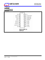
1 General
1.1 Pin Assignment
MPC82L(E)52
This document information is the intellectual property of Megawin Technology Co., Ltd.
Megawin Technology Co., Ltd. 1999 All right reserved.
Version: 1.1 09/2006
5
MEGAWIN
MAKE YOU WIN
MPC82L52/54
MPC82E52/54
MPC82L(E)54
This document information is the intellectual property of Megawin Technology Co., Ltd.
Megawin Technology Co., Ltd. 1999 All right reserved.
Version: 1.1 09/2006
6
MPC82L52/54
MPC82E52/54
MEGAWIN
MAKE YOU WIN
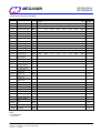
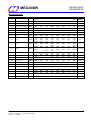
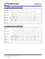
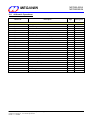
1.2 Special Function Registers (SFRs)
MPC82L(E)52 SFRs
SYMBOL
ACC*
B*
PSW *
DESCRIPTION
ADDR
Accumulator
E0H
B Register
F0H
BIT ADDRESS & SYMBOL
MSB
LSB
RESET
VALUE
00H
00H
D7H
CY
D6H
AC
D5H
F0
D4H
RS1
D3H
RS0
D2H
OV
D1H
-
D0H
P
Program Status Word
D0H
Stack Pointer
81H
07H
DPH
Data Pointer High
83H
00H
DPL
Data Pointer Low
82H
SP
000000x0B
00H
97H
P1.7
AIN7
SPICLK
B7H
P3.7
CEX0
96H
P1.6
AIN6
MISO
B6H
-
95H
P1.5
AIN5
MOSI
B5H
P3.5
T1
CEX1
BDH
94H
P1.4
AIN4
/SS
B4H
P3.4
T0
ECI
BCH
PS
ACH
ES
93H
P1.3
AIN3
92H
P1.2
AIN2
91H
P1.1
AIN1
90H
P1.0
AIN0
B3H
P3.3
/INT1
B2H
P3.2
/INT0
B1H
P3.1
TXD
B0H
P3.0
RXD
BBH
PT1
ABH
ET1
BAH
PX1
AAH
EX1
B9H
PT0
A9H
ET0
B8H
PX0
A8H
EX0
P1*
Port 1
90H
P3*
Port 3
B0H
IP*
Interrupt Priority
B8H
IE*
Interrupt Enable
A8H
Timer Mode
89H
GATE
C/-T
M1
M0
GATE
C/-T
M1
M0
00H
8FH
TF1
8EH
TR1
8DH
TF0
8CH
TR0
8BH
IE1
8AH
IT1
89H
IE0
88H
IT0
00H
TMOD
BFH
AFH
EA
BEH
PPCA_LVD PSPI_ADC
AEH
ADH
EPCA_LVD ESPI_ADC
FFH
1x111111B
x0000000B
00H
TCON*
Timer Control
88H
TH0
Timer 0 High
8CH
00H
TL0
Timer 0 Low
8AH
00H
TH1
Timer 1 High
8DH
00H
TL1
Timer 1 Low
8BH
SCON*
Serial Port Control
98H
SBUF
Serial Data Buffer
99H
PCON
Power Control
87H
00H
9FH
SM0/FE
9EH
SM1
9DH
SM2
9BH
TB8
9AH
RB8
99H
TI
98H
RI
00H
xxH
SMOD
SMOD0
LVF
This document information is the intellectual property of Megawin Technology Co., Ltd.
Megawin Technology Co., Ltd. 1999 All right reserved.
Version: 1.1 09/2006
9CH
REN
POF
GF1
GF0
PD
IDL
00xx0000B
7
MPC82L52/54
MPC82E52/54
MEGAWIN
MAKE YOU WIN
The following SFRs are new added.
SYMBOL
DESCRIPTION
ADDR
BIT ADDRESS & SYMBOL
MSB
AUXR
Auxiliary Register
8EH
T0X12
PCON2
Power Control 2
C7H
-
RESET
VALUE
T1X12
URM0X6
EADCI
ESPI
ENLVFI
-
-
000000xxB
-
-
-
-
CKS2
CKS1
CKS0
xxxxx000B
PSH
PT1H
PX1H
PT0H
PX0H
x0000000B
PPCAH_ PSPIH_
LVD
ADC
IPH
Interrupt Priority High
B7H
SADEN
Slave Address Mask
B9H
00H
SADDR
Slave Address
A9H
00H
ADCTL
ADC Control Register
C5H
ADCI
ADCS
CHS2
CHS1
CHS0
00H
ADC Result
C6H
B7
B6
B5
B4
B3
B2
B1
B0
xxH
Watch-dog Timer
E1H
WRF
-
ENW
CLRW
WIDL
PS2
PS1
PS0
0x000000B
P1M0
Port1 Mode Register 0
91H
P1M0.7
P1M0.6
P1M0.5
P1M0.4
P1M0.3
P1M0.2
P1M0.1
P1M0.0
00H
P1M1
Port1 Mode Register 1
92H
P1M1.7
P1M1.6
P1M1.5
P1M1.4
P1M1.3
P1M1.2
P1M1.1
P1M1.0
00H
P3M0
Port3 Mode Register 0
B1H
P3M0.7
-
P3M0.5
P3M0.4
P3M0.3
P3M0.2
P3M0.1
P3M0.0
00H
P3M1
Port3 Mode Register 1
B2H
P3M1.7
-
P3M1.5
P3M1.4
P3M1.3
P3M1.2
P3M1.1
P3M1.0
00H
D8H
DFH
CF
DEH
CR
DDH
-
DCH
-
DBH
-
DAH
-
D9H
CCF1
D8H
CCF0
00xxxx00B
D9H
CIDL
-
-
-
-
CPS2
CPS1
ECF
0xxxx000B
ADC
WDTCR
CCON*
CMOD
PCA Counter
Control Register
PCA Counter
Mode Register
-
LSB
ADCON SPEED1 SPEED0
CH
PCA Counter, HB
F9H
00H
CL
PCA Counter, LB
E9H
00H
CCAPM0
CCAPM1
CCAP0H
CCAP0L
CCAP1H
CCAP1L
PCA Module0
Com/Cap Register
PCA Module1
Com/Cap Register
PCA Module0 Capture
Register, HB
PCA Module0 Capture
Register, LB
PCA Module1 Capture
Register, HB
PCA Module1 Capture
Register, LB
DAH
-
ECOM0
CAPP0
CAPN0
MAT0
TOG0
PWM0
ECCF0 x0000000B
DBH
-
ECOM1
CAPP1
CAPN1
MAT1
TOG1
PWM1
ECCF1 x0000000B
FAH
00H
EAH
00H
FBH
00H
EBH
00H
PCAPWM0 PWM Mode, auxiliary 0
F2H
-
-
-
-
-
-
ECAP0H ECAP0L xxxxxx00B
PCAPWM1 PWM Mode, auxiliary 1
F3H
-
-
-
-
-
-
ECAP1H ECAP1L xxxxxx00B
SPSTAT
SPI Status Register
84H
SPIF
WCOL
-
-
-
-
-
-
00xxxxxxB
SPCTL
SPI Control Register
85H
SSIG
SPEN
DORD
MSTR
CPOL
CPHA
SPR1
SPR0
04H
SPDAT
SPI Data Register
86H
ISPCR
ISP Control Register
E7H
ISPEN
SWBS
SWRST
CFAIL
-
ICK2
ICK1
ICK0
0000x000B
ISP Flash Mode Table
E5H
-
-
-
-
-
-
MS1
MS0
xxxxx000B
IFMT
IFADRH
IFADRL
ISP Flash Address
High
ISP Flash Address
Low
00H
E3H
00H
E4H
00H
IFD
ISP Flash Data
E2H
00H
SCMD
ISP Sequential
Command
E6H
xxH
Notes:
*: bit addressable
-: reserved bit
This document information is the intellectual property of Megawin Technology Co., Ltd.
Megawin Technology Co., Ltd. 1999 All right reserved.
Version: 1.1 09/2006
8
MPC82L52/54
MPC82E52/54
MEGAWIN
MAKE YOU WIN
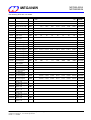
MPC82L(E)54 SFRs
SYMBOL
ACC*
B*
PSW *
DESCRIPTION
ADDR
Accumulator
E0H
B Register
F0H
BIT ADDRESS & SYMBOL
MSB
LSB
RESET
VALUE
00H
00H
D7H
CY
D6H
AC
D5H
F0
D4H
RS1
D3H
RS0
D2H
OV
D1H
-
D0H
P
Program Status Word
D0H
Stack Pointer
81H
07H
DPH
Data Pointer High
83H
00H
DPL
Data Pointer Low
82H
SP
P0*
Port 0
80H
P1*
Port 1
90H
P2*
Port 2
A0H
P3*
Port 3
B0H
IP*
Interrupt Priority
B8H
IE*
TMOD
000000x0B
00H
87H
P0.7
97H
P1.7
AIN7
SPICLK
A7H
P2.7
86H
P0.6
96H
P1.6
AIN6
MISO
A6H
P2.6
85H
P0.5
95H
P1.5
AIN5
MOSI
A5H
P2.5
B7H
P3.7
CEX0
B6H
-
B5H
P3.5
T1
CEX1
BDH
BFH
AFH
EA
BEH
PPCA_LVD PSPI_ADC
AEH
ADH
84H
P0.4
94H
P1.4
AIN4
/SS
A4H
P2.4
CEX3
B4H
P3.4
T0
ECI
BCH
PS
ACH
ES
83H
P0.3
93H
P1.3
AIN3
82H
P0.2
92H
P1.2
AIN2
81H
P0.1
91H
P1.1
AIN1
80H
P0.0
90H
P1.0
AIN0
A3H
P2.3
A2H
P2.2
A1H
P2.1
B3H
P3.3
/INT1
B2H
P3.2
/INT0
B1H
P3.1
TXD
A0H
P2.0
CEX2
B0H
P3.0
RXD
BBH
PT1
ABH
ET1
BAH
PX1
AAH
EX1
B9H
PT0
A9H
ET0
B8H
PX0
A8H
EX0
FFH
FFH
FFH
1x111111B
x0000000B
Interrupt Enable
A8H
Timer Mode
89H
GATE
C/-T
M1
M0
GATE
C/-T
M1
M0
00H
8FH
TF1
8EH
TR1
8DH
TF0
8CH
TR0
8BH
IE1
8AH
IT1
89H
IE0
88H
IT0
00H
EPCA_LVD ESPI_ADC
00H
TCON*
Timer Control
88H
TH0
Timer 1 High
8CH
00H
TL0
Timer 0 Low
8AH
00H
TH1
Timer 1 High
8DH
00H
TL1
Timer 0 Low
8BH
SCON*
Serial Port Control
98H
SBUF
Serial Data Buffer
99H
PCON
Power Control
87H
00H
9FH
SM0/FE
9EH
SM1
9DH
SM2
9BH
TB8
9AH
RB8
99H
TI
98H
RI
00H
xxH
SMOD
SMOD0
LVF
This document information is the intellectual property of Megawin Technology Co., Ltd.
Megawin Technology Co., Ltd. 1999 All right reserved.
Version: 1.1 09/2006
9CH
REN
POF
GF1
GF0
PD
IDL
00xx0000B
9
MPC82L52/54
MPC82E52/54
MEGAWIN
MAKE YOU WIN
The following SFRs are new added.
SYMBOL
DESCRIPTION
ADDR
BIT ADDRESS & SYMBOL
MSB
AUXR
Auxiliary Register
8EH
T0X12
PCON2
Power Control 2
C7H
-
RESET
VALUE
T1X12
URM0X6
EADCI
ESPI
ENLVFI
-
-
000000xxB
-
-
-
-
CKS2
CKS1
CKS0
xxxxx000B
PSH
PT1H
PX1H
PT0H
PX0H
x0000000B
PPCAH_ PSPIH_
LVD
ADC
IPH
Interrupt Priority High
B7H
SADEN
Slave Address Mask
B9H
00H
SADDR
Slave Address
A9H
00H
ADCTL
ADC Control Register
C5H
ADCH
ADC Result,
Higher 8 bits
ADC Result,
Lower 2 bits
-
LSB
ADCON SPEED1 SPEED0
ADCI
ADCS
CHS2
CHS1
CHS0
00H
C6H
B9
B8
B7
B6
B5
B4
B3
B2
xxH
BEH
-
-
-
-
-
-
B1
B0
xxH
Watch-dog Timer
E1H
WRF
-
ENW
CLRW
WIDL
PS2
PS1
PS0
0x000000B
P0M0
Port0 Mode Register 0
93H
-
-
-
-
P0M0.3
P0M0.2
P0M0.1
P0M0.0
00H
P0M1
Port0 Mode Register 1
94H
-
-
-
-
P0M1.3
P0M1.2
P0M1.1
P0M1.0
00H
P1M0
Port1 Mode Register 0
91H
P1M0.7
P1M0.6
P1M0.5
P1M0.4
P1M0.3
P1M0.2
P1M0.1
P1M0.0
00H
P1M1
Port1 Mode Register 1
92H
P1M1.7
P1M1.6
P1M1.5
P1M1.4
P1M1.3
P1M1.2
P1M1.1
P1M1.0
00H
P2M0
Port2 Mode Register 0
95H
P2M0.7
P2M0.6
P2M0.5
P2M0.4
P2M0.3
P2M0.2
P2M0.1
P2M0.0
00H
P2M1
Port2 Mode Register 1
96H
P2M1.7
P2M1.6
P2M1.5
P2M1.4
P2M1.3
P2M1.2
P2M1.1
P2M1.0
00H
P3M0
Port3 Mode Register 0
B1H
P3M0.7
-
P3M0.5
P3M0.4
P3M0.3
P3M0.2
P3M0.1
P3M0.0
00H
Port3 Mode Register 1
B2H
P3M1.7
-
P3M1.5
P3M1.4
P3M1.3
P3M1.2
P3M1.1
P3M1.0
00H
D8H
DFH
CF
DEH
CR
DDH
-
DCH
-
DBH
CCF3
DAH
CCF2
D9H
CCF1
D8H
CCF0
00xxxx00B
D9H
CIDL
-
-
-
-
CPS2
CPS1
ECF
0xxxx000B
ADCL
WDTCR
P3M1
CCON*
CMOD
PCA Counter
Control Register
PCA Counter
Mode Register
CH
PCA Counter, HB
F9H
00H
CL
PCA Counter, LB
E9H
00H
CCAPM0
CCAPM1
CCAPM2
CCAPM3
CCAP0H
CCAP0L
CCAP1H
CCAP1L
CCAP2H
CCAP2L
CCAP3H
CCAP3L
PCA Module0
Com/Cap Register
PCA Module1
Com/Cap Register
PCA Module2
Com/Cap Register
PCA Module3
Com/Cap Register
PCA Module0 Capture
Register, HB
PCA Module0 Capture
Register, LB
PCA Module1 Capture
Register, HB
PCA Module1 Capture
Register, LB
PCA Module2 Capture
Register, HB
PCA Module2 Capture
Register, LB
PCA Module3 Capture
Register, HB
PCA Module3 Capture
Register, LB
DAH
-
ECOM0
CAPP0
CAPN0
MAT0
TOG0
PWM0
ECCF0 x0000000B
DBH
-
ECOM1
CAPP1
CAPN1
MAT1
TOG1
PWM1
ECCF1 x0000000B
DCH
-
ECOM2
CAPP2
CAPN2
MAT2
TOG2
PWM2
ECCF2 x0000000B
DDH
-
ECOM3
CAPP3
CAPN3
MAT3
TOG3
PWM3
ECCF3 x0000000B
FAH
00H
EAH
00H
FBH
00H
EBH
00H
FCH
00H
ECH
00H
FDH
00H
EDH
00H
This document information is the intellectual property of Megawin Technology Co., Ltd.
Megawin Technology Co., Ltd. 1999 All right reserved.
Version: 1.1 09/2006
10
MPC82L52/54
MPC82E52/54
MEGAWIN
MAKE YOU WIN
(Continued)
PWM Mode,
0
PWM Mode,
PCAPWM1
1
PWM Mode,
PCAPWM2
2
PWM Mode,
PCAPWM3
3
PCAPWM0
SPSTAT
auxiliary
F2H
-
-
-
-
-
-
ECAP0H ECAP0L xxxxxx00B
F3H
-
-
-
-
-
-
ECAP1H ECAP1L xxxxxx00B
F4H
-
-
-
-
-
-
ECAP2H ECAP2L xxxxxx00B
F5H
-
-
-
-
-
-
ECAP3H ECAP3L xxxxxx00B
SPI Status Register
84H
SPIF
WCOL
-
-
-
-
-
-
00xxxxxxB
SSIG
SPEN
DORD
MSTR
CPOL
CPHA
SPR1
SPR0
04H
auxiliary
auxiliary
auxiliary
SPCTL
SPI Control Register
85H
SPDAT
SPI Data Register
86H
ISPCR
ISP Control Register
E7H
ISPEN
SWBS
SWRST
CFAIL
-
ICK2
ICK1
ICK0
0000x000B
ISP Flash Mode Table
E5H
-
-
-
-
-
-
MS1
MS0
xxxxx000B
IFMT
IFADRH
IFADRL
ISP Flash Address
High
ISP Flash Address
Low
00H
E3H
00H
E4H
00H
IFD
ISP Flash Data
E2H
00H
SCMD
ISP Sequential
Command
E6H
xxH
Notes:
*: bit addressable
-: reserved bit
This document information is the intellectual property of Megawin Technology Co., Ltd.
Megawin Technology Co., Ltd. 1999 All right reserved.
Version: 1.1 09/2006
11
MPC82L52/54
MPC82E52/54
MEGAWIN
MAKE YOU WIN
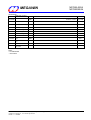
1.3 Flash Memory Configuration
MPC82L(E)52
(With total Flash Memory = 8K bytes)
0x0000
Note:
(1) ISP start address has four options:
0x1400 if ISP=3KB, or
0x1800 if ISP=2KB, or
0x1C00 if ISP=1KB, or
0x2000 if no ISP.
Application
code
AP-memory
(2) IAP lower boundary = [IAPLB]x256.
(3) IAP higher boundary = ISP start address - 1.
Total Flash Memory
IAP lower boundary
8KB
Nonvolatile
data
IAP-memory
ISP code
ISP-memory
IAP higher boundary
ISP start address
3KB/2KB/1KB/0KB
0x1FFF
MPC82L52
MPC82E52
MPC82L(E)54
(With total Flash Memory = 15.5K bytes)
0x0000
Note:
(1) ISP start address has four options:
0x3000 if ISP=3.5KB, or
0x3400 if ISP=2.5KB, or
0x3800 if ISP=1.5KB, or
0x3E00 if no ISP.
Application
code
AP-memory
(2) IAP lower boundary = [IAPLB]x256.
(3) IAP higher boundary = ISP start address - 1.
Total Flash Memory
IAP lower boundary
15.5KB
Nonvolatile
data
IAP-memory
IAP higher boundary
ISP start address
ISP code
ISP-memory
3.5KB/2.5KB/1.5KB/0KB
0x3DFF
MPC82L54
MPC82E54
This document information is the intellectual property of Megawin Technology Co., Ltd.
Megawin Technology Co., Ltd. 1999 All right reserved.
Version: 1.1 09/2006
12
MPC82L52/54
MPC82E52/54
MEGAWIN
MAKE YOU WIN
2 I/O Ports
The MPC82L(E)52 has two I/O ports: P1 and P3; while the MPC82L(E)54 has four I/O ports: P0, P1, P2 and P3.
The exact number of I/O pins available depends on their package type (see the following Table).
Table: I/O Pins Available v.s. Package Type
SkinnyDIP-20
SOP-20
(15 I/O pins)
SkinnyDIP-28
SOP-28
SSOP-28
PLCC-32
(27 I/O pins)
(23 I/O pins)
MPC82L(E)52
P1.0~P1.7 (8)
P3.0~P3.5, P3.7 (7)
-
-
MPC82L(E)54
P1.0~P1.7 (8)
P3.0~P3.5, P3.7 (7)
P1.0~P1.7 (8)
P2.0~P2.7 (8)
P3.0~P3.5, P3.7 (7)
P0.0~P0.3 (4)
P1.0~P1.7 (8)
P2.0~P2.7 (8)
P3.0~P3.5, P3.7 (7)
2.1 Port Configurations
All these port pins can be individually and independently configured to one of four modes: quasi-bidirectional
(standard 8051 I/O port), push-pull output, open-drain output or input-only (high-impedance). All port pins are in
the quasi-bidirectional mode after power-up or reset. Each port pin has a Schmitt-triggered input to improve
input noise rejection. Each port has two configuration registers to configure the I/O type for each port pin (see
the following Table).
Table : Port Configuration Settings
PxM0.y
PxM1.y
Port Mode
0
0
Quasi-bidirectional
0
1
Push-Pull Output
1
0
Input-Only (High Impedance, Hi-Z)
1
1
Open-Drain Output
Where x=0, 1, 2, or 3, and y=0~7. Registers PxM0 and PxM1 are described as follows.
P0M0 (Port0 Mode Register 0)
7
6
5
-
4
-
3
P0M0.3
2
P0M0.2
1
P0M0.1
0
P0M0.0
P0M1 (Port0 Mode Register 1)
7
6
5
-
4
-
3
P0M1.3
2
P0M1.2
1
P0M1.1
0
P0M1.0
P1M0 (Port1 Mode Register 0)
7
6
5
4
P1M0.7 P1M0.6 P1M0.5 P1M0.4
3
P1M0.3
2
P1M0.2
1
P1M0.1
0
P1M0.0
P1M1 (Port1 Mode Register 1)
7
6
5
4
P1M1.7 P1M1.6 P1M1.5 P1M1.4
3
P1M1.3
2
P1M1.2
1
P1M1.1
0
P1M1.0
This document information is the intellectual property of Megawin Technology Co., Ltd.
Megawin Technology Co., Ltd. 1999 All right reserved.
Version: 1.1 09/2006
13
MPC82L52/54
MPC82E52/54
MEGAWIN
MAKE YOU WIN
P2M0 (Port2 Mode Register 0)
7
6
5
4
P2M0.7 P2M0.6 P2M0.5 P2M0.4
3
P2M0.3
2
P2M0.2
1
P2M0.1
0
P2M0.0
P2M1 (Port2 Mode Register 1)
7
6
5
4
P2M1.7 P2M1.6 P2M1.5 P2M1.4
3
P2M1.3
2
P2M1.2
1
P2M1.1
0
P2M1.0
P3M0 (Port3 Mode Register 0)
7
6
5
4
P3M0.7
P3M0.5 P3M0.4
3
P3M0.3
2
P3M0.2
1
P3M0.1
0
P3M0.0
P3M1 (Port3 Mode Register 1)
7
6
5
4
P3M1.7
P3M1.5 P3M1.4
3
P3M1.3
2
P3M1.2
1
P3M1.1
0
P3M1.0
2.1.1 Quasi-bidirectional
Port pins in quasi-bidirectional mode are similar to the standard 8051 port pins. A quasi-bidirectional port can be
used as an input and output without the need to reconfigure the port. This is possible because when the port
outputs a logic high, it is weakly driven, allowing an external device to pull the pin low. When the pin outputs low,
it is driven strongly and able to sink a large current. There are three pull-up transistors in the quasi-bidirectional
output that serve different purposes.
One of these pull-ups, called the “very weak” pull-up, is turned on whenever the port register for the pin contains
a logic “1”. This very weak pull-up sources a very small current that will pull the pin high if it is left floating.
A second pull-up, called the “weak” pull-up, is turned on when the port register for the pin contains a logic “1”
and the pin itself is also at a logic “1” level. This pull-up provides the primary source current for a quasibidirectional pin that is outputting a 1. If this pin is pulled low by the external device, this weak pull-up turns off,
and only the very weak pull-up remains on. In order to pull the pin low under these conditions, the external
device has to sink enough current to over-power the weak pull-up and pull the port pin below its input threshold
voltage.
The third pull-up is referred to as the “strong” pull-up. This pull-up is used to speed up low-to-high transitions on
a quasi-bidirectional port pin when the port register changes from a logic “0” to a logic “1”. When this occurs, the
strong pull-up turns on for two CPU clocks, quickly pulling the port pin high.
This document information is the intellectual property of Megawin Technology Co., Ltd.
Megawin Technology Co., Ltd. 1999 All right reserved.
Version: 1.1 09/2006
14
MEGAWIN
MAKE YOU WIN
MPC82L52/54
MPC82E52/54
2.1.2 Open-Drain Output
The open-drain output configuration turns off all pull-ups and only drives the pull-down transistor of the port pin
when the port register contains a logic “0”. To use this configuration in application, a port pin must have an
external pull-up, typically a resistor tied to VDD. The pull-down for this mode is the same as for the quasibidirectional mode. In addition, the input path of the port pin in this configuration is also the same as quasibidirectional mode.
2.1.3 Input-Only (Hi-Z)
The input-only configuration is a Schmitt-triggered input without any pull-up resistors on the pin.
2.1.4 Push-Pull Output
The push-pull output configuration has the same pull-down structure as both the open-drain and the quasibidirectional output modes, but provides a continuous strong pull-up when the port register contains a logic “1”.
The push-pull mode may be used when more source current is needed from a port output. In addition, the input
path of the port pin in this configuration is also the same as quasi-bidirection mode.
This document information is the intellectual property of Megawin Technology Co., Ltd.
Megawin Technology Co., Ltd. 1999 All right reserved.
Version: 1.1 09/2006
15
MEGAWIN
MAKE YOU WIN
MPC82L52/54
MPC82E52/54
2.2 Maximum Ratings for Port Outputs
While port pins function as outputs (which can source or sink a current), to prevent the device from being
permanently damaged, users should take care the total current not more than 40mA for sourcing or sinking
regardless of a 3.3V device or a 5V device. That means that the device can source total 40mA and sink total
40mA at the same time without causing any damage to itself.
This document information is the intellectual property of Megawin Technology Co., Ltd.
Megawin Technology Co., Ltd. 1999 All right reserved.
Version: 1.1 09/2006
16
MEGAWIN
MAKE YOU WIN
MPC82L52/54
MPC82E52/54
3 On-chip expanded RAM (XRAM)
In addition to the standard 256 bytes of internal RAM, the MPC82L(E)54 has on-chip 256 bytes of expanded
RAM (XRAM). User can use “MOVX @Ri” or “MOVX @DPTR” to access them. Since these “MOVX”
instructions are modified for XRAM accessing, the I/O status of P0, P2 and P3.7 (/RD) are not affected while
these instructions are executed.
Using the XRAM in Software
For KEIL-C51 compiler, to assign the variables to be located at XRAM, the “pdata” or “xdata” definition should
be used. After being compiled, the variables declared by “pdata” and “xdata” will become the memories
accessed by “MOVX @Ri” and “MOVX @DPTR”, respectively. Thus the MPC82L(E)54 hardware can access
them correctly. The user can get the following descriptions from the “Keil Software — Cx51 Compiler User’s
Guide”.
This document information is the intellectual property of Megawin Technology Co., Ltd.
Megawin Technology Co., Ltd. 1999 All right reserved.
Version: 1.1 09/2006
17
MPC82L52/54
MPC82E52/54
MEGAWIN
MAKE YOU WIN
4 Timer 0 and Timer 1
After power-up or reset, the default function and operation of Timer 0 and Timer 1 is fully compatible with the
standard 8051 MCU. The only difference is that besides Fosc/12 the user can select an alternate clock source,
the Fosc. The bit-7 and bit-6 in AUXR provide this selection.
AUXR (Auxiliary Register)
7
6
5
4
T0X12
T1X12 URM0X6 EADCI
3
ESPI
2
ENLVFI
1
-
0
-
T0X12: Timer 0 clock source select. Set to select Fosc as the clock source, and clear to select Fosc/12.
T1X12: Timer 1 clock source select. Set to select Fosc as the clock source, and clear to select Fosc/12.
Note:
Both these two bits are 0 after power-up or reset, and thus select Fosc/12 as the clock source by default, like the
standard 8051 does.
The following figures show the selection of alternate clock source for Timer 0 and Timer1.
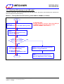
4.1 Mode 0
Where OSC means Fosc, the system clock.
4.2 Mode 1
Where OSC means Fosc, the system clock.
This document information is the intellectual property of Megawin Technology Co., Ltd.
Megawin Technology Co., Ltd. 1999 All right reserved.
Version: 1.1 09/2006
18
MEGAWIN
MAKE YOU WIN
MPC82L52/54
MPC82E52/54
4.3 Mode 2
Where OSC means Fosc, the system clock.
4.4 Mode 3
Where OSC means Fosc, the system clock.
This document information is the intellectual property of Megawin Technology Co., Ltd.
Megawin Technology Co., Ltd. 1999 All right reserved.
Version: 1.1 09/2006
19
MPC82L52/54
MPC82E52/54
MEGAWIN
MAKE YOU WIN
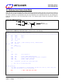
5 Serial Port
5.1 Baudrate Setting
All the four operation modes of the serial port are the same as those of the standard 8051 except the baudrate
setting. The bit-6 and bit-5 in AUXR provide a new option for the baudrate setting, as listed below.
Table: Baudrate Setting
Serial Port Mode
Compatible to standard 8051
Baudrate = Fosc/12
Baudrate = Fosc/2
if AUXR.5 (URM0X6) is 0
if AUXR.5 (URM0X6) is 1
Baudrate = (2SMOD/32) x Fosc/[12x(256-TH1)]
Baudrate = (2SMOD/32) x Fosc/(256-TH1)
if AUXR.6 (T1X12) is 0
if AUXR.6 (T1X12) is 1
Baudrate = (2SMOD/64) x Fosc
-
Mode 0
Mode 1 & 3
New option
Mode 2
Where Fosc is the system clock.
AUXR (Auxiliary Register)
7
6
5
4
T0X12
T1X12 URM0X6 EADCI
3
ESPI
2
ENLVFI
1
-
0
-
T1X12: Timer 1 clock source select. Set to select Fosc as the clock source, and clear to select Fosc/12.
URM0X6: Serial Port mode 0 baudrate select.
Note:
Since these two bits are 0 after any reset, it is compatible to the standard 8051 by default.
This document information is the intellectual property of Megawin Technology Co., Ltd.
Megawin Technology Co., Ltd. 1999 All right reserved.
Version: 1.1 09/2006
20
MPC82L52/54
MPC82E52/54
MEGAWIN
MAKE YOU WIN
5.2 Enhanced Feature: Frame Error Detection
While the SMOD0 bit (in PCON, bit 6) is set, the hardware will set the FE bit (SCON.7) when an invalid stop bit
is detected. The FE bit is not cleared by valid frames but should be cleared by software.
SCON (Serial Port Control Register)
7
6
5
4
SM0/FE
SM1
SM2
REN
3
TB8
2
RB8
1
TI
0
RI
SM0/FE:
SM0: Serial Port Mode bit0 (when SMOD0=0).
FE: Frame Error bit (when SMOD0=1).
PCON (Power Control Register)
7
6
5
4
SMOD SMOD0
LVF
POF
3
GF1
2
GF0
1
PD
0
IDL
SMOD0: Clear to let SCON.7 function as ‘SM0’, and set to let SCON.7 function as ‘FE’.
This document information is the intellectual property of Megawin Technology Co., Ltd.
Megawin Technology Co., Ltd. 1999 All right reserved.
Version: 1.1 09/2006
21
MEGAWIN
MAKE YOU WIN
MPC82L52/54
MPC82E52/54
5.3 Enhanced Feature: Automatic Address Recognition
Automatic Address Recognition is a feature which allows the UART to recognize certain addresses in the serial
bit stream by using hardware to make the comparisons. This feature saves a great deal of software overhead
by eliminating the need for the software to examine every serial address which passes by the serial port. This
feature is enabled by setting the SM2 bit in SCON. In the 9 bit UART modes, mode 2 and mode 3, the Receive
Interrupt flag (RI) will be automatically set when the received byte contains either the “Given” address or the
“Broadcast” address. The 9-bit mode requires that the 9th information bit is a 1 to indicate that the received
information is an address and not data. Automatic address recognition is shown in the following figure.
The 8 bit mode is called Mode 1. In this mode the RI flag will be set if SM2 is enabled and the information
received has a valid stop bit following the 8 address bits and the information is either a Given or Broadcast
address.
Mode 0 is the Shift Register mode and SM2 is ignored.
Using the Automatic Address Recognition feature allows a master to selectively communicate with one or more
slaves by invoking the Given slave address or addresses. All of the slaves may be contacted by using the
Broadcast address. Two special Function Registers are used to define the slave’s address, SADDR, and the
address mask, SADEN.
SADEN is used to define which bits in the SADDR are to be used and which bits are “don’t care”. The SADEN
mask can be logically ANDed with the SADDR to create the “Given” address which the master will use for
addressing each of the slaves. Use of the Given address allows multiple slaves to be recognized while
excluding others.
The following examples will help to show the versatility of this scheme:
Slave 0
SADDR = 1100 0000
SADEN = 1111 1101
Given = 1100 00X0
Slave 1
SADDR = 1100 0000
SADEN = 1111 1110
Given = 1100 000X
In the above example SADDR is the same and the SADEN data is used to differentiate between the two slaves.
Slave 0 requires a 0 in bit 0 and it ignores bit 1. Slave 1 requires a 0 in bit 1 and bit 0 is ignored. A unique
address for Slave 0 would be 1100 0010 since slave 1 requires a 0 in bit 1. A unique address for slave 1 would
be 1100 0001 since a 1 in bit 0 will exclude slave 0. Both slaves can be selected at the same time by an
address which has bit 0 = 0 (for slave 0) and bit 1 = 0 (for slave 1). Thus, both could be addressed with 1100
0000.
In a more complex system the following could be used to select slaves 1 and 2 while excluding slave 0:
Slave 0
SADDR = 1100 0000
SADEN = 1111 1001
Given = 1100 0XX0
Slave 1
SADDR = 1110 0000
SADEN = 1111 1010
Given = 1110 0X0X
This document information is the intellectual property of Megawin Technology Co., Ltd.
Megawin Technology Co., Ltd. 1999 All right reserved.
Version: 1.1 09/2006
22
MEGAWIN
MAKE YOU WIN
MPC82L52/54
MPC82E52/54
Slave 2
SADDR = 1110 0000
SADEN = 1111 1100
Given = 1110 00XX
In the above example the differentiation among the 3 slaves is in the lower 3 address bits. Slave 0 requires that
bit 0 = 0 and it can be uniquely addressed by 1110 0110. Slave 1 requires that bit 1 = 0 and it can be uniquely
addressed by 1110 0101. Slave 2 requires that bit 2 = 0 and its unique address is 1110 0011. To select Slaves
0 and 1 and exclude Slave 2 use address 1110 0100, since it is necessary to make bit 2 = 1 to exclude slave 2.
The Broadcast Address for each slave is created by taking the logical OR of SADDR and SADEN. Zeros in this
result are trended as don’t-cares. In most cases, interpreting the don’t-cares as ones, the broadcast address will
be FF hexadecimal.
Upon reset SADDR (SFR address 0A9H) and SADEN (SFR address 0B9H) are leaded with 0s. This produces a
given address of all “don’t cares” as well as a Broadcast address of all “don’t cares”. This effectively disables the
Automatic Addressing mode and allows the micro-controller to use standard 80C51 type UART drivers which do
not make use of this feature.
This document information is the intellectual property of Megawin Technology Co., Ltd.
Megawin Technology Co., Ltd. 1999 All right reserved.
Version: 1.1 09/2006
23
MEGAWIN
MAKE YOU WIN
MPC82L52/54
MPC82E52/54
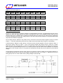
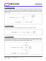
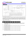
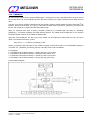
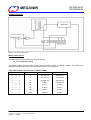
6 Serial Peripheral Interface (SPI)
The MPC82L(E)52/54 provide another high-speed serial communication interface, the SPI interface. SPI is a
full-duplex, high-speed and synchronous communication bus with two operation modes: Master mode and Slave
mode. Up to 3 Mbps can be supported in either Master or Slave mode under the 12MHz system clock. It has a
Transfer Completion Flag (SPIF) and Write Collision Flag (WCOL) in the SPI status register (SPSTAT register).
SPI Block Diagram
The SPI interface has four pins: SPICLK, MOSI, MISO and /SS:
• SPICLK, MOSI and MISO are typically tied together between two or more SPI devices. Data flows from master
to slave on the MOSI (Master Out Slave In) pin and flows from slave to master on the MISO (Master In Slave
Out) pin. The SPICLK signal is output in the master mode and is input in the slave mode. If the SPI system is
disabled, i.e. SPEN (SPCTL.6) = 0, these pins function as normal I/O pins.
• /SS is the optional slave select pin. In a typical configuration, an SPI master asserts one of its port pins to
select one SPI device as the current slave. An SPI slave device uses its SS pin to determine whether it is
selected. But if SPEN (SPCTL.6) = 0 or SSIG (SPCTL.7) = 1, the /SS pin is ignored.
Note that even if the SPI is configured as a master (MSTR = 1), it can still be converted to a slave by driving the
/SS pin low (if SSIG = 0). Should this happen, the SPIF bit (SPSTAT.7) will be set. See section "Mode change
on /SS-pin".
The following special function registers are related to the SPI operation.
This document information is the intellectual property of Megawin Technology Co., Ltd.
Megawin Technology Co., Ltd. 1999 All right reserved.
Version: 1.1 09/2006
24
MPC82L52/54
MPC82E52/54
MEGAWIN
MAKE YOU WIN
SPCTL (SPI Control Register)
7
6
5
SSIG
SPEN
DORD
4
MSTR
3
CPOL
2
CPHA
1
SPR1
0
SPR0
SSIG: /SS is ignored
If SSIG=1, MSTR decides whether the device is a master or slave.
If SSIG=0, the /SS pin decides whether the device is a master or slave.
SPEN: SPI enable
If SPEN=1, the SPI is enabled.
If SPEN=0, the SPI interface is disabled and all SPI pins will be general-purpose I/O ports.
DORD: SPI data order
1 : The LSB of the data byte is transmitted first.
0 : The MSB of the data byte is transmitted first.
MSTR: Master/Slave mode select
CPOL: SPI clock polarity select
1: SPICLK is high when idle. The leading edge of SPICLK is the falling edge and the trailing edge is
the rising edge.
0: SPICLK is low when idle. The leading edge of SPICLK is the rising edge and the trailing edge is
the falling edge.
CPHA: SPI clock phase select
1: Data is driven on the leading edge of SPICLK, and is sampled on the trailing edge.
0: Data is driven when /SS pin is low (SSIG=0) and changes on the trailing edge of SPICLK. Data is
sampled on the leading edge of SPICLK.
(Note : If SSIG=1, CPHA must not be 1, otherwise the operation is not defined.)
SPR1-SPR0: SPI clock rate select (when in master mode)
00 : Fosc/4
01 : Fosc/16
10 : Fosc/64
11 : Fosc/128
Where, Fosc is the system clock.
SPSTAT (SPI Status Register)
7
6
5
SPIF
WCOL
-
4
-
3
-
2
-
1
-
0
-
SPIF: SPI transfer completion flag
When a serial transfer finishes, the SPIF bit is set and an interrupt is generated if the ESPI (AUXR.3) bit,
the ESPI_ADC (IE.5) bit and the EA (IE.7) bit are set. If /SS pin is driven low when SPI is in master mode
with SSIG=0, SPIF will also be set to signal the “mode change”. The SPIF is cleared in software by
writing ‘1’ to this bit.
WCOL: SPI write collision flag. The WCOL bit is set if the SPI data register, SPDAT, is written during a data
transfer. The WCOL flag is cleared in software by writing ‘1’ to this bit.
SPDAT (SPI Data Register)
7
6
5
(MSB)
4
3
2
1
0
(LSB)
SPI data buffer for transmit and receive.
This document information is the intellectual property of Megawin Technology Co., Ltd.
Megawin Technology Co., Ltd. 1999 All right reserved.
Version: 1.1 09/2006
25
MEGAWIN
MAKE YOU WIN
MPC82L52/54
MPC82E52/54
6.1 Typical SPI Configurations
6.1.1 Single Master & Single Slave
For the master: can use any port pin, including P1.4 (/SS), to drive the /SS pin of the slave.
For the slave: SSIG is ‘0’, and /SS pin is used to select the slave.
6.1.2 Dual Device, where either can be a Master or a Slave
Two devices are connected to each other and either device can be a master or a slave. When no SPI operation
is occurring, both can be configured as masters with MSTR=1, SSIG=0 and P1.4 (/SS) configured in quasibidirectional mode. When any device initiates a transfer, it can configure P1.4 as an output and drive it low to
force a “mode change to slave” in the other device.
This document information is the intellectual property of Megawin Technology Co., Ltd.
Megawin Technology Co., Ltd. 1999 All right reserved.
Version: 1.1 09/2006
26
MEGAWIN
MAKE YOU WIN
MPC82L52/54
MPC82E52/54
6.1.3 Single Master & Multiple Slaves
For the master: can use any port pin, including P1.4 (/SS) to drive the /SS pins of the slaves.
For all the slaves: SSIG is ‘0’, and are selected by their corresponding /SS pins.
This document information is the intellectual property of Megawin Technology Co., Ltd.
Megawin Technology Co., Ltd. 1999 All right reserved.
Version: 1.1 09/2006
27
MPC82L52/54
MPC82E52/54
MEGAWIN
MAKE YOU WIN
6.2 Configuring the SPI
Table: SPI Master and Slave Selection
SPEN
SSIG
(SPCTL.6) (SPCTL.7)
/SS
-pin
(SPCTL.4)
MSTR
0
X
X
X
1
0
0
0
1
0
1
0
1
0
0
1è0
Mode
MISO
-pin
MOSI
-pin
SPICLK
-pin
Remarks
SPI disabled
input
input
input
P1.4~P1.7 are used as general
port pins.
output
input
input
Selected as slave.
Hi-Z
input
input
Not selected.
output
input
input
Mode change to slave
if /SS pin is driven low, and
MSTR will be cleared to ‘0’ by
H/W automatically.
Hi-Z
Hi-Z
MOSI and SPICLK are at high
impedance to avoid bus
contention when the Master is
idle.
output
output
MOSI and SPICLK are push-pull
when the Master is active.
Salve
(selected)
Slave
(not selected)
Slave
(by mode
change)
Master
1
0
1
1
(idle)
input
Master
(active)
1
1
X
0
Slave
output
input
input
1
1
X
1
Master
input
output
output
“X” means “don’t care”.
6.2.1 Additional Considerations for a Slave
When CPHA is 0, SSIG must be 0 and /SS pin must be negated and reasserted between each successive serial
byte transfer. If the SPDAT register is written while /SS pin is active (low), a write collision error results and
WCOL is set. The operation is undefined if CPHA is 0 and SSIG is 1.
When CPHA is 1, SSIG may be 0 or 1. If SSIG=0, the /SS pin may remain active low between successive
transfers (can be tied low at all times). This format is sometimes preferred for use in systems having a signle
fixed master and a single slave configuration.
6.2.2 Additional Considerations for a Master
In SPI, transfers are always initiated by the master. If the SPI is enabled (SPEN=1) and selected as master,
writing to the SPI data register (SPDAT) by the master starts the SPI clock generator and data transfer. The
data will start to appear on MOSI about one half SPI bit-time to one SPI bit-time after data is written to SPDAT.
Before starting the transfer, the master may select a slave by driving the /SS pin of the corresponding device
low. Data written to the SPDAT register of the master is shifted out of MOSI pin of the master to the MOSI pin of
the slave. And, at the same time the data in SPDAT register of the selected slave is shifted out on MISO pin to
the MISO pin of the master.
After shifting one byte, the SPI clock generator stops, setting the transfer completion flag (SPIF) and an interrupt
will be created if the SPI interrupt is enabled. The two shift registers in the master CPU and slave CPU can be
considered as one distributed 16-bit circular shift register. When data is shifted from the master to the slave,
data is also shifted in the opposite direction simultaneously. This means that during one shift cycle, data in the
master and the slave are interchanged.
This document information is the intellectual property of Megawin Technology Co., Ltd.
Megawin Technology Co., Ltd. 1999 All right reserved.
Version: 1.1 09/2006
28
MEGAWIN
MAKE YOU WIN
MPC82L52/54
MPC82E52/54
6.2.3 Mode Change on /SS-pin
If SPEN=1, SSIG=0, MSTR=1 and /SS pin=1, the SPI is enabled in master mode. In this case, another master
can drive this pin low to select this device as an SPI slave and start sending data to it. To avoid bus contention,
the SPI becomes a slave. As a result of the SPI becoming a slave, the MOSI and SPICLK pins are forced to be
an input and MISO becomes an output. The SPIF flag in SPSTAT is set, and if the SPI interrupt is enabled, an
SPI interrupt will occur. User software should always check the MSTR bit. If this bit is cleared by a slave select
and the user wants to continue to use the SPI as a master, the user must set the MSTR bit again, otherwise it
will stay in slave mode.
6.2.4 Write Collision
The SPI is single buffered in the transmit direction and double buffered in the receive direction. New data for
transmission can not be written to the shift register until the previous transaction is complete. The WCOL
(SPSTAT.6) bit is set to indicate data collision when the data register is written during transmission. In this case,
the data currently being transmitted will continue to be transmitted, but the new data, i.e., the one causing the
collision, will be lost.
While write collision is detected for both a master or a slave, it is uncommon for a master because the master
has full control of the transfer in progress. The slave, however, has no control over when the master will initiate
a transfer and therefore collision can occur.
For receiving data, received data is transferred into a parallel read data buffer so that the shift register is free to
accept a second character. However, the received character must be read from the Data Register (SPDAT)
before the next character has been completely shifted in. Otherwise. the previous data is lost.
WCOL can be cleared in software by writing ‘1’ to the bit.
6.2.5 SPI Clock Rate Select
The SPI clock rate selection (in master mode) uses the SPR1 and SPR0 bits in the SPCTL register, as shown
below.
SPR1, SPR0
-----------------0, 0
0, 1
1, 0
1, 1
SPI Clock Rate
------------------------Fosc/4
Fosc/16
Fosc/64
Fosc/128
Where, Fosc is the system clock.
This document information is the intellectual property of Megawin Technology Co., Ltd.
Megawin Technology Co., Ltd. 1999 All right reserved.
Version: 1.1 09/2006
29
MEGAWIN
MAKE YOU WIN
MPC82L52/54
MPC82E52/54
6.3 Data Mode
Clock Phase Bit (CPHA) allows the user to set the edges for sampling and changing data. The Clock Polarity bit,
CPOL, allows the user to set the clock polarity. The following figures show the different settings of CPHA.
6.3.1 SPI Slave Transfer Format with CPHA=0
6.3.2 SPI Slave Transfer Format with CPHA=1
This document information is the intellectual property of Megawin Technology Co., Ltd.
Megawin Technology Co., Ltd. 1999 All right reserved.
Version: 1.1 09/2006
30
MEGAWIN
MAKE YOU WIN
MPC82L52/54
MPC82E52/54
6.3.3 SPI Master Transfer Format with CPHA=0
6.3.4 SPI Master Transfer Format with CPHA=1
This document information is the intellectual property of Megawin Technology Co., Ltd.
Megawin Technology Co., Ltd. 1999 All right reserved.
Version: 1.1 09/2006
31
MPC82L52/54
MPC82E52/54
MEGAWIN
MAKE YOU WIN
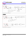
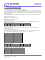
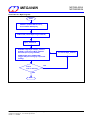
7 Programmable Counter Array (PCA)
7.1 Introduction to the PCA
The Programmable Counter Array (PCA) is a special 16-bit Timer that has four 16-bit capture/compare modules
associated with it. Each of the modules can be programmed to operate in one of four modes: rising and/or
falling edge capture, software timer, high-speed output, or PWM (pulse width modulation) output. Each module
has a pin associated with it: module 0 is connected to P3.7, module 1 to P3.5, module 2 to P2.0 and module 3
to P2.4. The basic PCA configuration is shown in the figure as follows.
PCA Configuration
The PCA timer is a common time base for all modules and can be programmed to run at: 1/12 the oscillator
frequency, 1/2 the oscillator frequency, the Timer 0 overflow, or the input on ECI pin (P3.4). The clock source for
the timer is determined by the CPS1 and CPS0 bits in the CMOD register as follows.
CMOD (PCA Counter Mode Register)
7
6
5
4
CIDL
CIDL:
3
-
2
CPS1
1
CPS0
0
ECF
PCA counter idle control.
CIDL=0 lets the PCA counter continue functioning during idle mode.
CIDL=1 lets the PCA counter be gated off during idle mode.
CPS1-CPS0: PCA counter clock source select bits.
0
0
Internal clock, Fosc/12 (Where, Fosc is the system clock.)
0
1
Internal clock, Fosc/2
1
0
Timer 0 overflow
1
1
External clock at the ECI pin (P3.4)
ECF:
Enable PCA counter overflow interrupt.
ECF=1 enables an interrupt when CF bit (in CCON register) is set.
In the CMOD SFR are two additional bits associated with the PCA. They are CIDL which allows the PCA to stop
during idle mode, and ECF which when set causes an interrupt if the PCA overflow flag CF (in the CCON SFR)
is set either when the counter overflows or by software. The following figure shows these functions.
This document information is the intellectual property of Megawin Technology Co., Ltd.
Megawin Technology Co., Ltd. 1999 All right reserved.
Version: 1.1 09/2006
32
MPC82L52/54
MPC82E52/54
MEGAWIN
MAKE YOU WIN
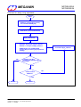
PCA Timer/Counter
Where OSC means Fosc, the system clock.
The CCON register contains the run control bit for the PCA and the flags for the PCA timer and each module.
To run the PCA the CR bit (CCON.6) must be set by software. The PCA is shut off by clearing this bit. The CF
bit (CCON.7) is set when the PCA counter overflows and an interrupt will be generated if the ECF bit in the
CMOD register is set. The CF bit can only be cleared by software. CCF0 ~ CCF3 are the flags for module 0 ~
module 3, respectively, and they are set by hardware when either a match or a capture occurs. These flags also
can only be cleared by software.
CCON (PCA Counter Control Register)
7
6
5
4
CF
CR
-
3
CCF3
2
CCF2
1
CCF1
0
CCF0
CF:
PCA Counter Overflow flag. Set by hardware when the counter rolls over. CF flag can generate an
interrupt if bit ECF in CMOD is set. CF may be set by either hardware or software but can only be
cleared by software.
CR:
PCA Counter Run control bit.
Set by software to turn the PCA counter on. Must be cleared by software to turn the PCA counter off.
CCF3: PCA Module 3 interrupt flag.
Set by hardware when a match or capture occurs. Must be cleared by software.
CCF2: PCA Module 2 interrupt flag.
Set by hardware when a match or capture occurs. Must be cleared by software.
CCF1: PCA Module 1 interrupt flag.
Set by hardware when a match or capture occurs. Must be cleared by software.
CCF0: PCA Module 0 interrupt flag.
Set by hardware when a match or capture occurs. Must be cleared by software.
This document information is the intellectual property of Megawin Technology Co., Ltd.
Megawin Technology Co., Ltd. 1999 All right reserved.
Version: 1.1 09/2006
33
MEGAWIN
MAKE YOU WIN
MPC82L52/54
MPC82E52/54
The PCA interrupt system is shown below.
PCA Interrupt System
Each module in the PCA has a special function register associated with it. These registers are CCAPMn, where
n = 0,1, 2 and 3 for module 0 to module 3, respectively. See the register description as follows.
CCAPM0/CCAPM1/CCAPM2/CCAPM3 (PCA Module Compare/Capture Registers)
7
6
5
4
3
2
1
0
ECOMn CAPPn CAPNn MATn
TOGn
PWMn ECCFn
ECOMn: Enable Comparator. ECOMn=1 enables the comparator function.
CAPPn: Capture Positive. CAPPn=1 enables positive edge capture.
CAPNn: Capture Negative. CAPNn=1 enables negative edge capture.
MATn:
Match control. When MATn=1, a match of the PCA counter with this module’s compare/capture
Register causes the CCFn bit in CCON to be set.
TOGn:
Toggle control. When TOGn=1, a match of the PCA counter with this module’s compare/capture
register causes the CEXn pin to toggle.
PWMn:
PWM control. PWMn=1 enables the CEXn pin to be used as a pulse width modulated
output.
ECCFn: Enable CCFn interrupt. Enables compare/capture flag CCFn in the CCON register to generate an
interrupt.
Note: The bits CAPNn (CCAPMn.4) and CAPPn (CCAPMn.5) determine the edge on which a capture input will
be active. If both bits are set, both edges will be enabled and a capture will occur for either transition.
This document information is the intellectual property of Megawin Technology Co., Ltd.
Megawin Technology Co., Ltd. 1999 All right reserved.
Version: 1.1 09/2006
34
MEGAWIN
MAKE YOU WIN
MPC82L52/54
MPC82E52/54
There are two additional registers associated with each of the PCA modules: CCAPnH and CCAPnL. They are
the registers that store the 16-bit count when a capture occurs or a compare should occur.
When a module is used in the PWM mode, in addition to the above two registers, an extended register
PCAPWMn is used to improve the range of the duty cycle of the output. The improved range of the duty cycle
starts from 0%, up to 100%, with a step of 1/256.
PCAPWM0/PCAPWM1/PCAPWM2/PCAPWM3 (PWM Mode Auxiliary Registers)
7
6
5
4
3
2
1
0
ECAPnH ECAPnL
ECAPnH: Extended 9th bit (MSB bit), associated with CCAPnH to become a 9-bit register used in PWM mode.
ECAPnL: Extended 9th bit (MSB bit), associated with CCAPnL to become a 9-bit register used in PWM mode.
This document information is the intellectual property of Megawin Technology Co., Ltd.
Megawin Technology Co., Ltd. 1999 All right reserved.
Version: 1.1 09/2006
35
MPC82L52/54
MPC82E52/54
MEGAWIN
MAKE YOU WIN
7.2 Operation Modes of the PCA
The following Table shows the CCAPMn register settings for the various PCA functions.
Table: PCA Module Modes
ECOMn CAPPn CAPNn MATn
TOGn PWMn ECCFn
Module Function
0
0
0
0
0
0
0
No operation
X
1
0
0
0
0
X
16-bit capture by a positive-edge trigger on CEXn
X
0
1
0
0
0
X
16-bit capture by a negative-edge trigger on CEXn
X
1
1
0
0
0
X
16-bit capture by a transition on CEXn
1
0
0
1
0
0
X
16-bit Software Timer
1
0
0
1
1
0
X
16-bit High Speed Output
1
0
0
0
0
1
0
8-bit Pulse Width Modulator (PWM)
7.2.1 Capture Mode
To use one of the PCA modules in the capture mode, either one or both of the bits CAPN and CAPP for that
module must be set. The external CEX input for the module is sampled for a transition. When a valid transition
occurs the PCA hardware loads the value of the PCA counter registers (CH and CL) into the module’s capture
registers (CCAPnL and CCAPnH). If the CCFn and the ECCFn bits for the module are both set, an interrupt will
be generated.
Function Block Diagram
This document information is the intellectual property of Megawin Technology Co., Ltd.
Megawin Technology Co., Ltd. 1999 All right reserved.
Version: 1.1 09/2006
36
MEGAWIN
MAKE YOU WIN
MPC82L52/54
MPC82E52/54
7.2.2 16-bit Software Timer Mode
The PCA modules can be used as software timers by setting both the ECOM and MAT bits in the module’s
CCAPMn register. The PCA timer will be compared to the module’s capture registers, and when a match occurs
an interrupt will occur if the CCFn and the ECCFn bits for the module are both set.
Function Block Diagram
7.2.3 High Speed Output Mode
In this mode the CEX output associated with the PCA module will toggle each time a match occurs between the
PCA counter and the module’s capture registers. To activate this mode, the TOG, MAT and ECOM bits in the
module’s CCAPMn register must be set.
Function Block Diagram
This document information is the intellectual property of Megawin Technology Co., Ltd.
Megawin Technology Co., Ltd. 1999 All right reserved.
Version: 1.1 09/2006
37
MEGAWIN
MAKE YOU WIN
MPC82L52/54
MPC82E52/54
7.2.4 PWM Mode
All of the PCA modules can be used as PWM outputs. The frequency of the output depends on the clock source
for the PCA timer. All of the modules will have the same frequency of output because they all share the PCA
timer.
The duty cycle of each module is determined by the module’s capture register CCAPnL and the extended 9th bit,
ECAPnL. When the 9-bit value of { 0, [CL] } is less than the 9-bit value of { ECAPnL, [CCAPnL] } the output will
be low, and if equal to or greater than the output will be high.
When CL overflows from 0xFF to 0x00, { ECAPnL, [CCAPnL] } is reloaded with the value of { ECAPnH,
[CCAPnH] }. This allows updating the PWM without glitches. The PWMn and ECOMn bits in the module’s
CCAPMn register must be set to enable the PWM mode.
Using the 9-bit comparison, the duty cycle of the output can be improved to really start from 0%, and up to
100%. The formula for the duty cycle is:
Duty Cycle = 1 – { ECAPnH, [CCAPnH] } / 256.
Where, [CCAPnH] is the 8-bit value of the CCAPnH register, and ECAPnH (bit-1 in the PCAPWMn register) is
1-bit value. So, { ECAPnH, [CCAPnH] } forms a 9-bit value for the 9-bit comparator.
For examples,
a. If ECAPnH=0 & CCAPnH=0x00 (i.e., 0x000), the duty cycle is 100%.
b. If ECAPnH=0 & CCAPnH=0x40 (i.e., 0x040) the duty cycle is 75%.
c. If ECAPnH=0 & CCAPnH=0xC0 (i.e., 0x0C0), the duty cycle is 25%.
d. If ECAPnH=1 & CCAPnH=0x00 (i.e., 0x100), the duty cycle is 0%.
Function Block Diagram
This document information is the intellectual property of Megawin Technology Co., Ltd.
Megawin Technology Co., Ltd. 1999 All right reserved.
Version: 1.1 09/2006
38
MPC82L52/54
MPC82E52/54
MEGAWIN
MAKE YOU WIN
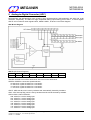
8 Analog-to-Digital Converter (ADC)
MPC82L(E)52 and MPC82L(E)54 have a built-in ADC (implemented by SAR approach) with 8-bit and 10-bit
resolution, respectively. The ADC has eight multiplexed analog inputs sharing pins of Port 1, a control register
ADCTL and conversion result registers ADC, ADCH & ADCL, as shown in the block diagram.
ADC Block Diagram
ADCTL (AD Control Register)
7
6
5
ADCON SPEED1 SPEED0
4
ADCI
3
ADCS
2
CHS2
1
CHS1
0
CHS0
ADCON: Cleared to turn off the ADC block. Set to turn on the ADC block.
SPEED1~SPEED0: conversion speed selection.
00: 840 clock cycles are taken for a conversion.
01: 630 clock cycles are taken for a conversion.
10: 420 clock cycles are taken for a conversion.
11: 210 clock cycles are taken for a conversion.
ADCS : ADC start bit, which is set by software and automatically cleared by hardware.
ADCI : ADC interrupt flag, which is set by hardware and should be cleared by software.
CHS2~CHS0: channel selection.
000: select P1.0 as the analog input
001: select P1.1 as the analog input
010: select P1.2 as the analog input
011: select P1.3 as the analog input
100: select P1.4 as the analog input
101: select P1.5 as the analog input
110: select P1.6 as the analog input
111: select P1.7 as the analog input
This document information is the intellectual property of Megawin Technology Co., Ltd.
Megawin Technology Co., Ltd. 1999 All right reserved.
Version: 1.1 09/2006
39
MEGAWIN
MAKE YOU WIN
MPC82L52/54
MPC82E52/54
Prior to using the ADC function, users should:
1) enable the ADC block by setting the ADCON bit,
2) select the analog input pin by bits CHS2~CHS0, and
3) configure the selected pin to its Input-Only mode by P1M0 and P1M1 registers.
Now, user can start the A-to-D conversion by setting the ADCS bit. The conversion time is controlled by bits
SPEED1 and SPEED0. Normally, 210 clock cycles are enough for a conversion under Fosc=12MHz. For higher
Fosc, 420 clock cycles may be needed.
Once the conversion is finished, the hardware will:
1) automatically clear the ADCS bit,
2) load the conversion result into the ADC register for MPC82L(E)52 and [ADCH, ADCL] registers for
MPC82L(E)54, and
3) set the interrupt flag ADCI.
User can check if the conversion is finished by polling the ADCI flag. If the ADC interrupt is enabled by setting
bits EADCI (AUXR.4) and ESPI_ADC (IE.5), the CPU will enter its Interrupt Service Routine when the
conversion is completed. And, the ADCI flag should be cleared by software. (Refer to Section 9 for interrupt of
the ADC.)
Note the ADC should be powered off before entering idle mode to reduce power consumption.
This document information is the intellectual property of Megawin Technology Co., Ltd.
Megawin Technology Co., Ltd. 1999 All right reserved.
Version: 1.1 09/2006
40
MPC82L52/54
MPC82E52/54
MEGAWIN
MAKE YOU WIN
9 Interrupt
The MPC82L(E)52/54 has a 9-source 4-level interrupt structure. The 9 interrupt sources and their interrupt
vectors are shown in the following table.
Table : Interrupt Sources
Source
Request Bits
Polling Priority
Vector Address
INT0
IE0
(highest priority)
0003H
Timer 0
TF0
.
000BH
INT1
IE1
.
0013H
Timer 1
TF1
.
001BH
Serial Port
RI+TI
.
0023H
SPI or ADC
SPIF+ADCI
.
002BH
PCA or
Low Voltage Detect
CF+CCFn+LVF
(n=0~3)
(lowest priority)
0033H
Note:
CCF2 and CCF3 are available only in MPC82L(E)54.
The following SFRs are associated with the interrupts. Among them, the IPH (Interrupt Priority High) register
makes the four-level interrupt structure possible.
IE (Interrupt Enable Register)
7
6
5
EA
EPCA_LVD ESPI_ADC
4
ES
3
ET1
2
EX1
1
ET0
0
EX0
EA: Global disable bit. If EA = 0, all interrupts are disabled. If EA = 1, each interrupt can be individually
enabled or disabled by setting or clearing its enable bit.
EPCA_LVD: PCA & LVD interrupts enable bit
ESPI_ADC: SPI & ADC interrupts enable bit.
ES: Serial Port interrupt enable bit.
ET1: Timer 1 interrupt enable bit.
EX1: External interrupt 1 enable bit.
ET0: Timer 0 interrupt enable bit.
EX0: External interrupt 0 enable bit.
IP (Interrupt Priority Register)
7
6
5
PPCA_LVD PSPI_ADC
4
PS
3
PT1
2
PX1
1
PT0
0
PX0
PPCA_LVD: PCA & LVD interrupts priority bit
PSPI_ADC: SPI & ADC interrupts priority bit.
PS: Serial Port interrupt priority bit.
PT1: Timer 1 interrupt priority bit.
PX1: External interrupt 1 priority bit.
PT0: Timer 0 interrupt priority bit.
PX0: External interrupt 0 priority bit.
This document information is the intellectual property of Megawin Technology Co., Ltd.
Megawin Technology Co., Ltd. 1999 All right reserved.
Version: 1.1 09/2006
41
MPC82L52/54
MPC82E52/54
MEGAWIN
MAKE YOU WIN
IPH (Interrupt Priority High Register)
7
6
5
PPCAH_LVD PSPIH_ADC
4
PSH
3
PT1H
2
PX1H
1
PT0H
0
PX0H
PPCAH_LVD: PCA & LVD interrupts priority bit high.
PSPIH_ADC: SPI & ADC interrupts priority bit high.
PSH: Serial Port interrupt priority bit high.
PT1H: Timer 1 interrupt priority bit high.
PX1H: External interrupt 1 priority bit high.
PT0H: Timer 0 interrupt priority bit high.
PX0H: External interrupt 0 priority bit high.
The IPH register, when combined with the IP register, determines the priority of each interrupt. The priority of
each interrupt is determined as shown in the following table:
IPH.x
IP.x
Interrupt Priority Level
1
1
0
0
1
0
1
0
Level 3 (highest priority)
Level 2
Level 1
Level 0 (lowest priority)
For example, if (IPH.3, IP.3)=(1, 0), then Timer 1 has the priority level equal to 2, which is higher than level 1
with (IPH.3, IP.3)=(0, 1) or level 0 with (IPH.3, IP.3)=(0, 0).
This document information is the intellectual property of Megawin Technology Co., Ltd.
Megawin Technology Co., Ltd. 1999 All right reserved.
Version: 1.1 09/2006
42
MEGAWIN
MAKE YOU WIN
MPC82L52/54
MPC82E52/54
9.1 Interrupt Architecture
Note:
CCF2 and CCF3 are available only in MPC82L(E)54.
This document information is the intellectual property of Megawin Technology Co., Ltd.
Megawin Technology Co., Ltd. 1999 All right reserved.
Version: 1.1 09/2006
43
MEGAWIN
MAKE YOU WIN
MPC82L52/54
MPC82E52/54
9.2 Note on Interrupt during ISP/IAP
During ISP/IAP, the CPU halts for a while for internal ISP/IAP processing. At this time, the interrupt will queue
up for being serviced if the interrupt is enabled previously. Once the ISP/IAP is complete, the CPU continues
running and the interrupts in the queue will be serviced immediately if the interrupt flag is still active. Users,
however, should be aware of the following:
(1) Any interrupt can not be serviced in time during the CPU halts for ISP/IAP processing.
(2) The low-level triggered external interrupts, /INT0 and /INT1, should keep active until the ISP/IAP is
complete, or they will be neglected.
This document information is the intellectual property of Megawin Technology Co., Ltd.
Megawin Technology Co., Ltd. 1999 All right reserved.
Version: 1.1 09/2006
44
MPC82L52/54
MPC82E52/54
MEGAWIN
MAKE YOU WIN
10 One-time Enabled Watchdog Timer (WDT)
The WDT is intended as a recovery method in situations where the CPU may be subjected to software upset.
The WDT consists of a 15-bit free-running counter, an 8-bit prescaler and a control register (WDTCR). To
enable the WDT, users must set ENW bit (WDTCR.5). When the WDT is enabled, the counter will increment
one by an interval of (12 x Prescaler / Fosc). And now the user needs to clear it by writing “1” to the CLRW bit
(WDTCR.4) before WDT overflows. When WDT overflows, the MCU will reset itself and re-start.
Why is the WDT called “One-time Enabled”? It is because: Once the WDT is enabled (ENW=1), there is no way
to disable it except power-on reset (ENW=0). The WDTCR register will keep the previous programmed value
unchanged after hardware (RST-pin) reset, software reset and WDT reset. For example, if the WDTCR is 0x2D,
it still keeps at 0x2D rather than 0x00 after these resets. Only power-on reset can initialize it to 0x00.
WDTCR (Watch-Dog-Timer Control Register)
7
6
5
4
3
WRF
ENW
CLRW
WIDL
2
PS2
1
PS1
0
PS0
Note: This is a Write-only register.
WRF: WDT reset flag. When WDT overflows, this bit is set by H/W. It should be cleared by software.
ENW: Enable WDT. Set to enable WDT. (Note: Once set, it can only be cleared by power-on reset.)
CLRW: Clear WDT. “Writing 1” to this bit will clear WDT. (Note: It has no need to be cleared by “writing 0”.)
WIDL: WDT in Idle mode. Set this bit to let WDT keep counting while the MCU is in the Idle mode.
PS2~PS1: Prescaler select. See the following Table.
PS2 PS1 PS0
0
0
0
0
0
1
0
1
0
0
1
1
1
0
0
1
0
1
1
1
0
1
1
1
Prescaler value
2
4
8
16
32
64
128
256
In addition to being initialized by software, the WDTCR register can also be automatically initialized at power-up
by the hardware options HWENW, HWWIDL and HWPS[2:0], which should be programmed by a universal
Writer or Programmer, as described below.
If HWENW is programmed to “enabled”, then hardware will automatically do the following initialization for the
WDTCR register at power-up:
(1) set ENW bit,
(2) load HWWIDL into WIDL bit, and
(3) load HWPS[2:0] into PS[2:0] bits.
For example:
If HWWIDL and HWPS[2:0] are programmed to be 1 and 5, respectively, then WDTCR will be initialized to be
0x2D when MCU is powered up, as shown below.
This document information is the intellectual property of Megawin Technology Co., Ltd.
Megawin Technology Co., Ltd. 1999 All right reserved.
Version: 1.1 09/2006
45
MPC82L52/54
MPC82E52/54
MEGAWIN
MAKE YOU WIN
WDT Block Diagram
Where, Fosc is the system clock.
WDT overflow period
The WDT overflow period is determined by the formula:
215 x (12 x Prescaler / Fosc).
The following Table shows the WDT overflow period for MCU running at 6MHz and 12MHz. The period is the
maximum interval for the user to clear the WDT to prevent from chip reset.
Table: WDT Overflow Period at Fosc = 6MHz & 12MHz
PS2 PS1 PS0
Prescaler value
Fosc=6MHz
Fosc=12MHz
0
0
0
2
131.072 ms
65.536 ms
0
0
1
4
262.144 ms
131.072 ms
0
1
0
8
524.288 ms
262.144 ms
0
1
1
16
1.048 s
524.288 ms
1
0
0
32
2.097 s
1.048 s
1
0
1
64
4.194 s
2.097 s
1
1
0
128
8.389 s
4.194 s
1
1
1
256
16.778 s
8.389 s
This document information is the intellectual property of Megawin Technology Co., Ltd.
Megawin Technology Co., Ltd. 1999 All right reserved.
Version: 1.1 09/2006
46
MEGAWIN
MAKE YOU WIN
MPC82L52/54
MPC82E52/54
Sample code for WDT
Condition: Fosc=6MHz
Target: WDT Overflow Period = 1.048 seconds
WDTCR_buf DATA
30h
;declare a buffer for WDTCR register
;(because WDTCR is a Write-only register)
MOV
WDTCR_buf,#00h
;clear buffer for WDTCR register
ANL
ORL
MOV
WDTCR_buf,#0F8h ;(PS2,PS1,PS0)=(0,1,1), prescaler=16
WDTCR_buf,#03h ;@Fosc=6MHz, WDT_Overflow_Period=1.048s
WDTCR,WDTCR_buf ;
ORL
MOV
WDTCR_buf,#20h ;enable WDT
WDTCR,WDTCR_buf ;write to WDTCR register
start:
;...
;...
main_loop:
ORL
MOV
;...
;...
JMP
ANL
MOV
WDTCR_buf,#10h ;clear WDT
WDTCR,WDTCR_buf ;
main_loop
WDTCR_buf,#0DFh ;disable WDT
WDTCR,WDTCR_buf ;
This document information is the intellectual property of Megawin Technology Co., Ltd.
Megawin Technology Co., Ltd. 1999 All right reserved.
Version: 1.1 09/2006
47
MPC82L52/54
MPC82E52/54
MEGAWIN
MAKE YOU WIN
11 In System Programming (ISP)
(First, please refer to Section 1.3 for Flash Memory Configuration.)
The Flash program memory supports both parallel programming and serial In-System Programming (ISP).
Parallel programming mode offers high-speed programming. ISP allows a device to be reprogrammed in the
end product under software control. The capability to field update the application firmware makes a wide range
of applications possible.
Prior to using the ISP feature, users should configure an ISP-memory using a universal Writer or Programmer.
Several SFRs are related to ISP:
IFADRH: ISP Flash address high register
IFADRL: ISP Flash address low register
IFD: ISP Flash data register
SCMD: ISP sequential command register (filled sequentially with 0x46 then 0xB9 to trigger ISP operation)
ISPCR (ISP Control Register)
7
6
5
4
ISPEN SWBS SWRST CFAIL
3
-
2
CKS2
1
CKS1
0
CKS0
ISPEN: Set to enable ISP function.
SWBS: Software boot select. Set to select booting from ISP-memory, and clear to select booting from APmemory after software reset.
SWRST: Write 1 to trigger software reset.
CFAIL: ISP fail flag. It is set by H/W if something error during ISP processing, and should be cleared by S/W.
CKS2~CKS0: Set the ISP timing according to Fosc (the system clock), as listed below.
Fosc
CKS2 CKS1 CKS0
30 ~ 24 MHz
24 ~ 20 MHz
20 ~ 12 MHz
12 ~ 6 MHz
6 ~ 3MHz
3 ~ 2MHz
2 ~ 1MHz
< 1MHz
0
0
0
0
1
1
1
1
IFMT (ISP Mode Register)
7
6
5
-
4
-
0
0
1
1
0
0
1
1
0
1
0
1
0
1
0
1
3
-
2
-
1
MS1
0
MS0
MS1 & MS0: Used to select the ISP mode, as listed below.
MS1
MS0
ISP Mode
0
0
1
1
0
1
0
1
Standby
Read
Byte Program
Page Erase
This document information is the intellectual property of Megawin Technology Co., Ltd.
Megawin Technology Co., Ltd. 1999 All right reserved.
Version: 1.1 09/2006
48
MPC82L52/54
MPC82E52/54
MEGAWIN
MAKE YOU WIN
11.1 Boot from ISP-memory to run “ISP code”
To run the “ISP code”, the CPU should boot from the ISP-memory. By means of the following two methods, the
CPU can boot from the ISP-memory.
Method 1: Directly Boot from ISP-memory (while HWBS or HWBS2 is enabled)
Start
Power on
(with HWBS=enabled and ISP-memory exists)
For MPC82L(E)54,
not only "Power on" but also "Reset from RST-pin"
if HWBS2=enabled and ISP-memory exists.
(And now, HWBS is "don't care".)
Now,
CPU will boot from ISP-memory,
and run "ISP code".
Check the user-defined
ISP condition, do ISP?
NO
YES
ISPEN=1 (enable ISP function),
and initialize ISPCR[2:0]
SWBS=0 (select boot from AP-memory)
SWRST=1 (trigger S/W reset)
Do ISP programming
to update the "Application code"
End
Now,
CPU will re-boot from AP-memory,
and run "Application code" normally.
This document information is the intellectual property of Megawin Technology Co., Ltd.
Megawin Technology Co., Ltd. 1999 All right reserved.
Version: 1.1 09/2006
49
MPC82L52/54
MPC82E52/54
MEGAWIN
MAKE YOU WIN
Method 2: Boot from ISP-memory through AP-memory (while HWBS and HWBS2 are disabled)
Start
Power on
(with HWBS=disabled and ISP-memory exists)
For MPC82L(E)54,
the HWBS2 must also be disabled.
Now,
CPU will boot from AP-memory,
and run "Application code".
Check the user-defined
ISP condition, do ISP?
NO
YES
SWBS=1 (select boot from ISP-memory)
SWRST=1 (trigger S/W reset)
Run "Application code"
normally
...
...
Now,
CPU will re-boot from ISP-memory,
and run "ISP code".
ISPEN=1 (enable ISP function),
and initialize ISPCR[2:0]
Do ISP programming
to update the "Application code"
...
End
This document information is the intellectual property of Megawin Technology Co., Ltd.
Megawin Technology Co., Ltd. 1999 All right reserved.
Version: 1.1 09/2006
50
MPC82L52/54
MPC82E52/54
MEGAWIN
MAKE YOU WIN
11.2 Operation Flow of ISP
The following figures show the flow chart for the various ISP modes used in the “ISP code” for ISP processing.
Flow Chart for “Page Erase”
Start
ISPEN=1 (enable ISP function),
and initialize ISPCR[2:0]
IFMT=0x03 (select Page Erase Mode)
Page_address=0
IFADRH= High-byte of Page_address
IFADRL= Low-byte of Page_address
Page_address=Page_address+0x0200
(Increment Page_address,
512 bytes per page)
SCMD=0x46, then SCMD=0xB9
(trigger ISP processing by sequential
writing)
Check
end of Page?
NO
YES
End
This document information is the intellectual property of Megawin Technology Co., Ltd.
Megawin Technology Co., Ltd. 1999 All right reserved.
Version: 1.1 09/2006
51
MPC82L52/54
MPC82E52/54
MEGAWIN
MAKE YOU WIN
Flow Chart for “Byte Program”
Start
ISPEN=1 (enable ISP function),
and initialize ISPCR[2:0]
IFMT=0x02 (select Byte Program Mode)
Byte_address=0
IFADRH= High-byte of Byte_address
IFADRL= Low-byte of Byte_address
IFD=data (to be programmed)
Increment Byte_address
SCMD=0x46, then SCMD=0xB9
(trigger ISP processing by sequential
writing)
Check
end of address?
NO
YES
End
This document information is the intellectual property of Megawin Technology Co., Ltd.
Megawin Technology Co., Ltd. 1999 All right reserved.
Version: 1.1 09/2006
52
MPC82L52/54
MPC82E52/54
MEGAWIN
MAKE YOU WIN
Flow Chart for “Verify” using “Byte Read”
Start
ISPEN=1 (enable ISP function),
and initialize ISPCR[2:0]
IFMT=0x01 (select Read Mode)
Byte_address=0
IFADRH= High-byte of Byte_address
IFADRL= Low-byte of Byte_address
SCMD=0x46, then SCMD=0xB9
(trigger ISP processing by sequential
writing)
NO
Increment Byte_address
Compare got data
(in IFD) with wanted data,
the same?
YES
Check end of
address?
NO
YES
ISP fail
ISP pass
This document information is the intellectual property of Megawin Technology Co., Ltd.
Megawin Technology Co., Ltd. 1999 All right reserved.
Version: 1.1 09/2006
53
MEGAWIN
MAKE YOU WIN
MPC82L52/54
MPC82E52/54
11.3 Demo of the “ISP code”
;******************************************************************************************
; ISP modes
;******************************************************************************************
IFD
IFADRH
IFADRL
IFMT
SCMD
ISPCR
;
DATA
DATA
DATA
DATA
DATA
DATA
0E2h
0E3h
0E4h
0E5h
0E6h
0E7h
MOV
ISPCR,#10000011b
;ISPCR.7=1, enable ISP
;ISPCR[2:0]=011, for Fosc=11.0592MHz
;=============================================================================
; 1. Page Erase Mode (512 bytes per page)
;=============================================================================
MOV
IFMT,#03h
;select Page Erase Mode
MOV
MOV
IFADRH,??
IFADRL,??
;fill page address in IFADRH & IFADRL
;
MOV
MOV
SCMD,#46h ;trigger ISP processing
SCMD,#0B9h ;
;Now in processing...(CPU will halt here until complete)
;=============================================================================
; 2. Byte Program Mode
;=============================================================================
MOV
IFMT,#02h
;select Byte Program Mode
MOV
MOV
MOV
IFADRH,??
IFADRL,??
IFD,??
;fill byte address in IFADRH & IFADRL
;
;fill the data to be programmed in IFD
MOV
MOV
SCMD,#46h ;trigger ISP processing
SCMD,#0B9h ;
;Now in processing...(CPU will halt here until complete)
;=============================================================================
; 3. Verify using Read Mode
;=============================================================================
MOV
IFMT,#01h
;select Byte Read Mode
MOV
MOV
IFADRH,??
IFADRL,??
;fill byte address in IFADRH & IFADRL
;
MOV
MOV
SCMD,#46h ;trigger ISP processing
SCMD,#0B9h ;
;Now in processing...(CPU will halt here until complete)
MOV
CJNE
...
...
ISP_error:
...
;
A,IFD
;data will be in IFD
A,wanted,ISP_error ;compare with the wanted value
This document information is the intellectual property of Megawin Technology Co., Ltd.
Megawin Technology Co., Ltd. 1999 All right reserved.
Version: 1.1 09/2006
54
MEGAWIN
MAKE YOU WIN
MPC82L52/54
MPC82E52/54
11.4 Note on In-System-Programming
During In-System-Programming, the CPU halts for a while for internal ISP processing. At this time, the interrupt
will queue up for being serviced if the interrupt is enabled previously. Once the ISP is complete, the CPU
continues running and the interrupts in the queue will be serviced immediately if the interrupt flag is still active.
Users, however, should be aware of the following:
(1) Any interrupt can not be serviced in time during the CPU halts for ISP processing.
(2) The low-level triggered external interrupts, /INT0 and /INT1, should keep active until the ISP is complete,
or they will be neglected.
This document information is the intellectual property of Megawin Technology Co., Ltd.
Megawin Technology Co., Ltd. 1999 All right reserved.
Version: 1.1 09/2006
55
MEGAWIN
MAKE YOU WIN
MPC82L52/54
MPC82E52/54
12 In Application Programming (IAP)
(First, please refer to Section 1.3 for Flash Memory Configuration.)
The MPC82L(E)52/54 is In Application Programmable (IAP), which allows some region in the Flash memory to
be used as non-volatile data storage while the application program is running. This useful feature can be applied
to the application where the data must be kept after power off. Thus, there is no need to use an external serial
EEPROM (such as 93C46, 24C01, .., and so on) for saving the non-volatile data.
12.1 IAP-memory Boundary/Range
In fact, the operating of IAP is the same as that of ISP except the Flash range to be programmed is different.
The for ISP is located within the AP-memory, while the range for IAP is located within the configured IAPmemory.
Prior to using the IAP feature, users should configure an IAP-memory by programming a proper value to the
option IAPLB[7:0] using a universal Writer or Programmer. The range of the IAP-memory depends on the
contents of IAPLB, as listed below.
IAP lower boundary = IAPLB[7:0]x256, and
IAP higher boundary = ISP start address –1.
Where, the IAPLB must be an even number.
Section 12.3 lists all the possible ranges for IAP-memory versus different ISP size and programmed IAPLB.
12.2 Update the data in the IAP-memory
Because the IAP-memory is a part of Flash memory, only Page Erase is provided for Flash erasing. To update
“one byte” in the IAP-memory, users can not directly program the new datum into that byte. The following steps
show the correct updating procedure:
Step1)
Step2)
Step3)
Step4)
Save the whole page data (512 bytes) to a buffer (also with size of 512 bytes).
Erase this page (using Page Erase mode of ISP).
Update the wanted byte(s) in the buffer.
Program the updated data out of the buffer into this page (using Byte Program mode of ISP).
To read the data in the IAP-memory, users can use either the “MOVC A,@A+DPTR” instruction or the Read
mode of ISP.
Users might ask: Where is the buffer?. The buffer comes from the internal RAM. The buffer size, however, might
not be 512 bytes due to the limitation of RAM size. According to the available size of the internal RAM (which
can be dedicated for the buffer), we can know how many bytes in each Flash page can be used as the nonvolatile storage. That is, if 128 bytes can be dedicated for the buffer, then only 128 bytes in each page can be
used, as the following Figure shows. (Of course, if only 64 bytes dedicated for the buffer, then 128 is replaced
with 64.)
In detailed description, if the available buffer size is 128 bytes, and total 260 bytes of non-volatile storage are
needed, the user should configure 1.5K bytes (3 Flash pages, because 260=128+128+4 è 3 pages) of IAPmemory for this application.
This document information is the intellectual property of Megawin Technology Co., Ltd.
Megawin Technology Co., Ltd. 1999 All right reserved.
Version: 1.1 09/2006
56
MPC82L52/54
MPC82E52/54
MEGAWIN
MAKE YOU WIN
IAP lower boundary
only 128 bytes used
One Flash page,
512 bytes
only 128 bytes used
One Flash page,
512 bytes
only 128 bytes used
One Flash page,
512 bytes
IAP-memory
.
.
.
only 128 bytes used
One Flash page,
512 bytes
IAP higher boundary
12.3 IAP-memory vs. Settings of ISP-memory and IAPLB
As we have known, the IAP-memory and ISP-memory are user-configured. Table 12.3a ~ Table 12.3h show a
variety of settings.
12.3.1 MPC82L(E)52 IAP-memory
Table 12.3a: No ISP
For MPC82L(E)52
Available
IAPLB
AP-memory
Range (Size)
IAP_low_boundary
0x02
0x04
0x06
0x08
0x0A
0x0C
0x0E
0x10
0x12
0x14
0x16
0x18
0x1A
0x1C
0x1E
>= 0x20
0x0000 ~ 0x01FF (0.5KB)
0x0000 ~ 0x03FF (1.0KB)
0x0000 ~ 0x05FF (1.5KB)
0x0000 ~ 0x07FF (2.0KB)
0x0000 ~ 0x09FF (2.5KB)
0x0000 ~ 0x0BFF (3.0KB)
0x0000 ~ 0x0DFF (3.5KB)
0x0000 ~ 0x0FFF (4.0KB)
0x0000 ~ 0x11FF (4.5KB)
0x0000 ~ 0x13FF (5.0KB)
0x0000 ~ 0x15FF (5.5KB)
0x0000 ~ 0x17FF (6.0KB)
0x0000 ~ 0x19FF (6.5KB)
0x0000 ~ 0x1BFF (7.0KB)
0x0000 ~ 0x1DFF (7.5KB)
0x0000 ~ 0x1FFF (8.0KB)
0x0200
0x0400
0x0600
0x0800
0x0A00
0x0C00
0x0E00
0x1000
0x1200
0x1400
0x1600
0x1800
0x1A00
0x1C00
0x1E00
(NA)
This document information is the intellectual property of Megawin Technology Co., Ltd.
Megawin Technology Co., Ltd. 1999 All right reserved.
Version: 1.1 09/2006
IAP-memory
Range (Size)
0x0200 ~ 0x1FFF (7.5KB)
0x0400 ~ 0x1FFF (7.0KB)
0x0600 ~ 0x1FFF (6.5KB)
0x0800 ~ 0x1FFF (6.0KB)
0x0A00 ~ 0x1FFF (5.5KB)
0x0C00 ~ 0x1FFF (5.0KB)
0x0E00 ~ 0x1FFF (4.5KB)
0x1000 ~ 0x1FFF (4.0KB)
0x1200 ~ 0x1FFF (3.5KB)
0x1400 ~ 0x1FFF (3.0KB)
0x1600 ~ 0x1FFF (2.5KB)
0x1800 ~ 0x1FFF (2.0KB)
0x1A00 ~ 0x1FFF (1.5KB)
0x1C00 ~ 0x1FFF (1.0KB)
0x1E00 ~ 0x1FFF (0.5KB)
(NA)
57
MPC82L52/54
MPC82E52/54
MEGAWIN
MAKE YOU WIN
Table 12.3b: ISP=1KB (ISP start address=0x1C00)
For MPC82L(E)52
Available
IAPLB
AP-memory
Range (Size)
IAP_low_boundary
0x02
0x04
0x06
0x08
0x0A
0x0C
0x0E
0x10
0x12
0x14
0x16
0x18
0x1A
>= 0x1C
0x0000 ~ 0x01FF (0.5KB)
0x0000 ~ 0x03FF (1.0KB)
0x0000 ~ 0x05FF (1.5KB)
0x0000 ~ 0x07FF (2.0KB)
0x0000 ~ 0x09FF (2.5KB)
0x0000 ~ 0x0BFF (3.0KB)
0x0000 ~ 0x0DFF (3.5KB)
0x0000 ~ 0x0FFF (4.0KB)
0x0000 ~ 0x11FF (4.5KB)
0x0000 ~ 0x13FF (5.0KB)
0x0000 ~ 0x15FF (5.5KB)
0x0000 ~ 0x17FF (6.0KB)
0x0000 ~ 0x19FF (6.5KB)
0x0000 ~ 0x1BFF (7.0KB)
0x0200
0x0400
0x0600
0x0800
0x0A00
0x0C00
0x0E00
0x1000
0x1200
0x1400
0x1600
0x1800
0x1A00
(NA)
IAP-memory
Range (Size)
0x0200 ~ 0x1BFF (6.5KB)
0x0400 ~ 0x1BFF (6.0KB)
0x0600 ~ 0x1BFF (5.5KB)
0x0800 ~ 0x1BFF (5.0KB)
0x0A00 ~ 0x1BFF (4.5KB)
0x0C00 ~ 0x1BFF (4.0KB)
0x0E00 ~ 0x1BFF (3.5KB)
0x1000 ~ 0x1BFF (3.0KB)
0x1200 ~ 0x1BFF (2.5KB)
0x1400 ~ 0x1BFF (2.0KB)
0x1600 ~ 0x1BFF (1.5KB)
0x1800 ~ 0x1BFF (1.0KB)
0x1A00 ~ 0x1BFF (0.5KB)
(NA)
Table 12.3c: ISP=2KB (ISP start address=0x1800)
For MPC82L(E)52
Available
IAPLB
AP-memory
Range (Size)
IAP_low_boundary
0x02
0x04
0x06
0x08
0x0A
0x0C
0x0E
0x10
0x12
0x14
0x16
>= 0x18
0x0000 ~ 0x01FF (0.5KB)
0x0000 ~ 0x03FF (1.0KB)
0x0000 ~ 0x05FF (1.5KB)
0x0000 ~ 0x07FF (2.0KB)
0x0000 ~ 0x09FF (2.5KB)
0x0000 ~ 0x0BFF (3.0KB)
0x0000 ~ 0x0DFF (3.5KB)
0x0000 ~ 0x0FFF (4.0KB)
0x0000 ~ 0x11FF (4.5KB)
0x0000 ~ 0x13FF (5.0KB)
0x0000 ~ 0x15FF (5.5KB)
0x0000 ~ 0x17FF (6.0KB)
0x0200
0x0400
0x0600
0x0800
0x0A00
0x0C00
0x0E00
0x1000
0x1200
0x1400
0x1600
(NA)
IAP-memory
Range (Size)
0x0200 ~ 0x17FF (5.5KB)
0x0400 ~ 0x17FF (5.0KB)
0x0600 ~ 0x17FF (4.5KB)
0x0800 ~ 0x17FF (4.0KB)
0x0A00 ~ 0x17FF (3.5KB)
0x0C00 ~ 0x17FF (3.0KB)
0x0E00 ~ 0x17FF (2.5KB)
0x1000 ~ 0x17FF (2.0KB)
0x1200 ~ 0x17FF (1.5KB)
0x1400 ~ 0x17FF (1.0KB)
0x1600 ~ 0x17FF (0.5KB)
(NA)
Table 12.3d: ISP=3KB (ISP start address=0x1400)
For MPC82L(E)52
Available
IAPLB
AP-memory
Range (Size)
IAP_low_boundary
0x02
0x04
0x06
0x08
0x0A
0x0C
0x0E
0x10
0x12
>= 0x14
0x0000 ~ 0x01FF (0.5KB)
0x0000 ~ 0x03FF (1.0KB)
0x0000 ~ 0x05FF (1.5KB)
0x0000 ~ 0x07FF (2.0KB)
0x0000 ~ 0x09FF (2.5KB)
0x0000 ~ 0x0BFF (3.0KB)
0x0000 ~ 0x0DFF (3.5KB)
0x0000 ~ 0x0FFF (4.0KB)
0x0000 ~ 0x11FF (4.5KB)
0x0000 ~ 0x13FF (5.0KB)
0x0200
0x0400
0x0600
0x0800
0x0A00
0x0C00
0x0E00
0x1000
0x1200
(NA)
This document information is the intellectual property of Megawin Technology Co., Ltd.
Megawin Technology Co., Ltd. 1999 All right reserved.
Version: 1.1 09/2006
IAP-memory
Range (Size)
0x0200 ~ 0x13FF (4.5KB)
0x0400 ~ 0x13FF (4.0KB)
0x0600 ~ 0x13FF (3.5KB)
0x0800 ~ 0x13FF (3.0KB)
0x0A00 ~ 0x13FF (2.5KB)
0x0C00 ~ 0x13FF (2.0KB)
0x0E00 ~ 0x13FF (1.5KB)
0x1000 ~ 0x13FF (1.0KB)
0x1200 ~ 0x13FF (0.5KB)
(NA)
58
MPC82L52/54
MPC82E52/54
MEGAWIN
MAKE YOU WIN
12.3.2 MPC82L(E)54 IAP-memory
Table 12.3e: No ISP
For MPC82L(E)54
Available
IAPLB
AP-memory
Range (Size)
IAP_low_boundary
0x02
0x04
0x06
0x08
0x0A
0x0C
0x0E
0x10
0x12
0x14
0x16
0x18
0x1A
0x1C
0x1E
0x20
0x22
0x24
0x26
0x28
0x2A
0x2C
0x2E
0x30
0x32
0x34
0x36
0x38
0x3A
0x3C
>= 0x3E
0x0000 ~ 0x01FF (0.5KB)
0x0000 ~ 0x03FF (1.0KB)
0x0000 ~ 0x05FF (1.5KB)
0x0000 ~ 0x07FF (2.0KB)
0x0000 ~ 0x09FF (2.5KB)
0x0000 ~ 0x0BFF (3.0KB)
0x0000 ~ 0x0DFF (3.5KB)
0x0000 ~ 0x0FFF (4.0KB)
0x0000 ~ 0x11FF (4.5KB)
0x0000 ~ 0x13FF (5.0KB)
0x0000 ~ 0x15FF (5.5KB)
0x0000 ~ 0x17FF (6.0KB)
0x0000 ~ 0x19FF (6.5KB)
0x0000 ~ 0x1BFF (7.0KB)
0x0000 ~ 0x1DFF (7.5KB)
0x0000 ~ 0x1FFF (8.0KB)
0x0000 ~ 0x21FF (8.5KB)
0x0000 ~ 0x23FF (9.0KB)
0x0000 ~ 0x25FF (9.5KB)
0x0000 ~ 0x27FF (10.0KB)
0x0000 ~ 0x29FF (10.5KB)
0x0000 ~ 0x2BFF (11.0KB)
0x0000 ~ 0x2DFF (11.5KB)
0x0000 ~ 0x2FFF (12.0KB)
0x0000 ~ 0x31FF (12.5KB)
0x0000 ~ 0x33FF (13.0KB)
0x0000 ~ 0x35FF (13.5KB)
0x0000 ~ 0x37FF (14.0KB)
0x0000 ~ 0x39FF (14.5KB)
0x0000 ~ 0x3BFF (15.0KB)
0x0000 ~ 0x3DFF (15.5KB)
0x0200
0x0400
0x0600
0x0800
0x0A00
0x0C00
0x0E00
0x1000
0x1200
0x1400
0x1600
0x1800
0x1A00
0x1C00
0x1E00
0x2000
0x2200
0x2400
0x2600
0x2800
0x2A00
0x2C00
0x2E00
0x3000
0x3200
0x3400
0x3600
0x3800
0x3A00
0x3C00
(NA)
This document information is the intellectual property of Megawin Technology Co., Ltd.
Megawin Technology Co., Ltd. 1999 All right reserved.
Version: 1.1 09/2006
IAP-memory
Range (Size)
0x0200 ~ 0x3DFF (15.0KB)
0x0400 ~ 0x3DFF (14.5KB)
0x0600 ~ 0x3DFF (14.0KB)
0x0800 ~ 0x3DFF (13.5KB)
0x0A00 ~ 0x3DFF (13.0KB)
0x0C00 ~ 0x3DFF (12.5KB)
0x0E00 ~ 0x3DFF (12.0KB)
0x1000 ~ 0X3DFF (11.5KB)
0x1200 ~ 0x3DFF (11.0KB)
0x1400 ~ 0x3DFF (10.5KB)
0x1600 ~ 0x3DFF (10.0KB)
0x1800 ~ 0x3DFF (9.5KB)
0x1A00 ~ 0x3DFF (9.0KB)
0x1C00 ~ 0x3DFF (8.5KB)
0x1E00 ~ 0x3DFF (8.0KB)
0x2000 ~ 0X3DFF (7.5KB)
0x2200 ~ 0x3DFF (7.0KB)
0x2400 ~ 0x3DFF (6.5KB)
0x2600 ~ 0x3DFF (6.0KB)
0x2800 ~ 0x3DFF (5.5KB)
0x2A00 ~ 0x3DFF (5.0KB)
0x2C00 ~ 0x3DFF (4.5KB)
0x2E00 ~ 0x3DFF (4.0KB)
0x3000 ~ 0X3DFF (3.5KB)
0x3200 ~ 0x3DFF (3.0KB)
0x3400 ~ 0x3DFF (2.5KB)
0x3600 ~ 0x3DFF (2.0KB)
0x3800 ~ 0x3DFF (1.5KB)
0x3A00 ~ 0x3DFF (1.0KB)
0x3C00 ~ 0x3DFF (0.5KB)
(NA)
59
MPC82L52/54
MPC82E52/54
MEGAWIN
MAKE YOU WIN
Table 12.3f: ISP=1.5KB (ISP start address=0x3800)
For MPC82L(E)54
Available
IAPLB
AP-memory
Range (Size)
IAP_low_boundary
0x02
0x04
0x06
0x08
0x0A
0x0C
0x0E
0x10
0x12
0x14
0x16
0x18
0x1A
0x1C
0x1E
0x20
0x22
0x24
0x26
0x28
0x2A
0x2C
0x2E
0x30
0x32
0x34
0x36
>= 0x38
0x0000 ~ 0x01FF (0.5KB)
0x0000 ~ 0x03FF (1.0KB)
0x0000 ~ 0x05FF (1.5KB)
0x0000 ~ 0x07FF (2.0KB)
0x0000 ~ 0x09FF (2.5KB)
0x0000 ~ 0x0BFF (3.0KB)
0x0000 ~ 0x0DFF (3.5KB)
0x0000 ~ 0x0FFF (4.0KB)
0x0000 ~ 0x11FF (4.5KB)
0x0000 ~ 0x13FF (5.0KB)
0x0000 ~ 0x15FF (5.5KB)
0x0000 ~ 0x17FF (6.0KB)
0x0000 ~ 0x19FF (6.5KB)
0x0000 ~ 0x1BFF (7.0KB)
0x0000 ~ 0x1DFF (7.5KB)
0x0000 ~ 0x1FFF (8.0KB)
0x0000 ~ 0x21FF (8.5KB)
0x0000 ~ 0x23FF (9.0KB)
0x0000 ~ 0x25FF (9.5KB)
0x0000 ~ 0x27FF (10.0KB)
0x0000 ~ 0x29FF (10.5KB)
0x0000 ~ 0x2BFF (11.0KB)
0x0000 ~ 0x2DFF (11.5KB)
0x0000 ~ 0x2FFF (12.0KB)
0x0000 ~ 0x31FF (12.5KB)
0x0000 ~ 0x33FF (13.0KB)
0x0000 ~ 0x35FF (13.5KB)
0x0000 ~ 0x37FF (14.0KB)
0x0200
0x0400
0x0600
0x0800
0x0A00
0x0C00
0x0E00
0x1000
0x1200
0x1400
0x1600
0x1800
0x1A00
0x1C00
0x1E00
0x2000
0x2200
0x2400
0x2600
0x2800
0x2A00
0x2C00
0x2E00
0x3000
0x3200
0x3400
0x3600
(NA)
This document information is the intellectual property of Megawin Technology Co., Ltd.
Megawin Technology Co., Ltd. 1999 All right reserved.
Version: 1.1 09/2006
IAP-memory
Range (Size)
0x0200 ~ 0x37FF (13.5KB)
0x0400 ~ 0x37FF (13.0KB)
0x0600 ~ 0x37FF (12.5KB)
0x0800 ~ 0x37FF (12.0KB)
0x0A00 ~ 0x37FF (11.5KB)
0x0C00 ~ 0x37FF (11.0KB)
0x0E00 ~ 0x37FF (10.5KB)
0x1000 ~ 0X37FF (10.0KB)
0x1200 ~ 0x37FF (9.5KB)
0x1400 ~ 0x37FF (9.0KB)
0x1600 ~ 0x37FF (8.5KB)
0x1800 ~ 0x37FF (8.0KB)
0x1A00 ~ 0x37FF (7.5KB)
0x1C00 ~ 0x37FF (7.0KB)
0x1E00 ~ 0x37FF (6.5KB)
0x2000 ~ 0X37FF (6.0KB)
0x2200 ~ 0x37FF (5.5KB)
0x2400 ~ 0x37FF (5.0KB)
0x2600 ~ 0x37FF (4.5KB)
0x2800 ~ 0x37FF (4.0KB)
0x2A00 ~ 0x37FF (3.5KB)
0x2C00 ~ 0x37FF (3.0KB)
0x2E00 ~ 0x37FF (2.5KB)
0x3000 ~ 0X37FF (2.0KB)
0x3200 ~ 0x37FF (1.5KB)
0x3400 ~ 0x37FF (1.0KB)
0x3600 ~ 0x37FF (0.5KB)
(NA)
60
MPC82L52/54
MPC82E52/54
MEGAWIN
MAKE YOU WIN
Table 12.3g: ISP=2.5KB (ISP start address=0x3400)
For MPC82L(E)54
Available
IAPLB
AP-memory
Range (Size)
IAP_low_boundary
0x02
0x04
0x06
0x08
0x0A
0x0C
0x0E
0x10
0x12
0x14
0x16
0x18
0x1A
0x1C
0x1E
0x20
0x22
0x24
0x26
0x28
0x2A
0x2C
0x2E
0x30
0x32
>= 0x34
0x0000 ~ 0x01FF (0.5KB)
0x0000 ~ 0x03FF (1.0KB)
0x0000 ~ 0x05FF (1.5KB)
0x0000 ~ 0x07FF (2.0KB)
0x0000 ~ 0x09FF (2.5KB)
0x0000 ~ 0x0BFF (3.0KB)
0x0000 ~ 0x0DFF (3.5KB)
0x0000 ~ 0x0FFF (4.0KB)
0x0000 ~ 0x11FF (4.5KB)
0x0000 ~ 0x13FF (5.0KB)
0x0000 ~ 0x15FF (5.5KB)
0x0000 ~ 0x17FF (6.0KB)
0x0000 ~ 0x19FF (6.5KB)
0x0000 ~ 0x1BFF (7.0KB)
0x0000 ~ 0x1DFF (7.5KB)
0x0000 ~ 0x1FFF (8.0KB)
0x0000 ~ 0x21FF (8.5KB)
0x0000 ~ 0x23FF (9.0KB)
0x0000 ~ 0x25FF (9.5KB)
0x0000 ~ 0x27FF (10.0KB)
0x0000 ~ 0x29FF (10.5KB)
0x0000 ~ 0x2BFF (11.0KB)
0x0000 ~ 0x2DFF (11.5KB)
0x0000 ~ 0x2FFF (12.0KB)
0x0000 ~ 0x31FF (12.5KB)
0x0000 ~ 0x33FF (13.0KB)
0x0200
0x0400
0x0600
0x0800
0x0A00
0x0C00
0x0E00
0x1000
0x1200
0x1400
0x1600
0x1800
0x1A00
0x1C00
0x1E00
0x2000
0x2200
0x2400
0x2600
0x2800
0x2A00
0x2C00
0x2E00
0x3000
0x3200
(NA)
This document information is the intellectual property of Megawin Technology Co., Ltd.
Megawin Technology Co., Ltd. 1999 All right reserved.
Version: 1.1 09/2006
IAP-memory
Range (Size)
0x0200 ~ 0x33FF (12.5kB)
0x0400 ~ 0x33FF (12.0KB)
0x0600 ~ 0x33FF (11.5KB)
0x0800 ~ 0x33FF (11.0KB)
0x0A00 ~ 0x33FF (10.5KB)
0x0C00 ~ 0x33FF (10.0KB)
0x0E00 ~ 0x33FF (9.5KB)
0x1000 ~ 0X33FF (9.0KB)
0x1200 ~ 0x33FF (8.5KB)
0x1400 ~ 0x33FF (8.0KB)
0x1600 ~ 0x33FF (7.5KB)
0x1800 ~ 0x33FF (7.0KB)
0x1A00 ~ 0x33FF (6.5KB)
0x1C00 ~ 0x33FF (6.0KB)
0x1E00 ~ 0x33FF (5.5KB)
0x2000 ~ 0X33FF (5.0KB)
0x2200 ~ 0x33FF (4.5KB)
0x2400 ~ 0x33FF (4.0KB)
0x2600 ~ 0x33FF (3.5KB)
0x2800 ~ 0x33FF (3.0KB)
0x2A00 ~ 0x33FF (2.5KB)
0x2C00 ~ 0x33FF (2.0KB)
0x2E00 ~ 0x33FF (1.5KB)
0x3000 ~ 0X33FF (1.0KB)
0x3200 ~ 0x33FF (0.5KB)
(NA)
61
MPC82L52/54
MPC82E52/54
MEGAWIN
MAKE YOU WIN
Table 12.3h: ISP=3.5KB (ISP start address=0x3000)
For MPC82L(E)54
Available
IAPLB
AP-memory
Range (Size)
IAP_low_boundary
0x02
0x04
0x06
0x08
0x0A
0x0C
0x0E
0x10
0x12
0x14
0x16
0x18
0x1A
0x1C
0x1E
0x20
0x22
0x24
0x26
0x28
0x2A
0x2C
0x2E
>= 0x30
0x0000 ~ 0x01FF (0.5KB)
0x0000 ~ 0x03FF (1.0KB)
0x0000 ~ 0x05FF (1.5KB)
0x0000 ~ 0x07FF (2.0KB)
0x0000 ~ 0x09FF (2.5KB)
0x0000 ~ 0x0BFF (3.0KB)
0x0000 ~ 0x0DFF (3.5KB)
0x0000 ~ 0x0FFF (4.0KB)
0x0000 ~ 0x11FF (4.5KB)
0x0000 ~ 0x13FF (5.0KB)
0x0000 ~ 0x15FF (5.5KB)
0x0000 ~ 0x17FF (6.0KB)
0x0000 ~ 0x19FF (6.5KB)
0x0000 ~ 0x1BFF (7.0KB)
0x0000 ~ 0x1DFF (7.5KB)
0x0000 ~ 0x1FFF (8.0KB)
0x0000 ~ 0x21FF (8.5KB)
0x0000 ~ 0x23FF (9.0KB)
0x0000 ~ 0x25FF (9.5KB)
0x0000 ~ 0x27FF (10.0KB)
0x0000 ~ 0x29FF (10.5KB)
0x0000 ~ 0x2BFF (11.0KB)
0x0000 ~ 0x2DFF (11.5KB)
0x0000 ~ 0x2FFF (12.0KB)
0x0200
0x0400
0x0600
0x0800
0x0A00
0x0C00
0x0E00
0x1000
0x1200
0x1400
0x1600
0x1800
0x1A00
0x1C00
0x1E00
0x2000
0x2200
0x2400
0x2600
0x2800
0x2A00
0x2C00
0x2E00
(NA)
This document information is the intellectual property of Megawin Technology Co., Ltd.
Megawin Technology Co., Ltd. 1999 All right reserved.
Version: 1.1 09/2006
IAP-memory
Range (Size)
0x0200 ~ 0x2FFF (11.5KB)
0x0400 ~ 0x2FFF (11.0KB)
0x0600 ~ 0x2FFF (10.5KB)
0x0800 ~ 0x2FFF (10.0KB)
0x0A00 ~ 0x2FFF (9.5KB)
0x0C00 ~ 0x2FFF (9.0KB)
0x0E00 ~ 0x2FFF (8.5KB)
0x1000 ~ 0X2FFF (8.0KB)
0x1200 ~ 0x2FFF (7.5KB)
0x1400 ~ 0x2FFF (7.0KB)
0x1600 ~ 0x2FFF (6.5KB)
0x1800 ~ 0x2FFF (6.0KB)
0x1A00 ~ 0x2FFF (5.5KB)
0x1C00 ~ 0x2FFF (5.0KB)
0x1E00 ~ 0x2FFF (4.5KB)
0x2000 ~ 0X2FFF (4.0KB)
0x2200 ~ 0x2FFF (3.5KB)
0x2400 ~ 0x2FFF (3.0KB
0x2600 ~ 0x2FFF (2.5KB)
0x2800 ~ 0x2FFF (2.0KB)
0x2A00 ~ 0x2FFF (1.5KB)
0x2C00 ~ 0x2FFF (1.0KB)
0x2E00 ~ 0x2FFF (0.5KB)
(NA)
62
MEGAWIN
MAKE YOU WIN
MPC82L52/54
MPC82E52/54
12.4 Note on In-Application-Programming
During In-Application-Programming, the CPU halts for a while for internal IAP processing. At this time, the
interrupt will queue up for being serviced if the interrupt is enabled previously. Once the IAP is complete, the
CPU continues running and the interrupts in the queue will be serviced immediately if the interrupt flag is still
active. Users, however, should be aware of the following:
(1) Any interrupt can not be serviced in time during the CPU halts for IAP processing.
(2) The low-level triggered external interrupts, /INT0 and /INT1, should keep active until the IAP is complete,
or they will be neglected.
This document information is the intellectual property of Megawin Technology Co., Ltd.
Megawin Technology Co., Ltd. 1999 All right reserved.
Version: 1.1 09/2006
63
MPC82L52/54
MPC82E52/54
MEGAWIN
MAKE YOU WIN
13 Programmable System Clock
The system clock (or CPU clock) of the device is programmable and source-selectable. The user can program
the system clock frequency by PCON2 register, and select the clock source by the hardware option bit
ENROSC, which can only be programmed by a universal Programmer/Writer. The following diagram shows the
clock structure.
System Clock Structure
Clock Divider
Xosc
XTAL1
000 (default)
001
010
011
100
101
110
111
/2
/4
/8
/16
/32
/64
/128
Divided Xosc
PCON2 (Power Control Register 2)
7
6
5
4
-
3
-
Fosc
System/CPU Clock
0
Selected by {CKS2,CKS1,CKS0}
Internal
RC Oscillator
1
RCosc
2
CKS2
ENROSC
Hareware Option
1: Disabled (default)
0: Enabled
1
CKS1
0
CKS0
CKS2, CKS1, CKS0: System clock select bits.
CKS2 CKS1 CKS0
-----------------------------0
0
0
0
0
1
0
1
0
0
1
1
1
0
0
1
0
1
1
1
0
1
1
1
Fosc (System clock)
---------------------------------------Xosc (default)
Xosc/2
Xosc/4
Xosc/8
Xosc/16
Xosc/32
Xosc/64
Xosc/128
Where, Xosc is the frequency of the signal on XTAL1-pin.
In the default state, the reset value of PCON2 is 0x00, so the system clock frequency is the same as that on the
XTAL1-pin. The user can modify PCON2 at any time to get a new system clock, which will be active just after
the modifying is completed.
This feature is especially useful for further power saving in idle mode as long as the user programs a non-zero
value to the CKS[2:0] bits before entering the idle mode.
This document information is the intellectual property of Megawin Technology Co., Ltd.
Megawin Technology Co., Ltd. 1999 All right reserved.
Version: 1.1 09/2006
64
MPC82L52/54
MPC82E52/54
MEGAWIN
MAKE YOU WIN
14 Wake-up from Power-down Mode
When the CPU is put into power-down mode, the external interrupts (/INT0 and /INT1) can be used to wake up
the CPU if any of them is enabled. Once the CPU is wakened up, the interrupt service routine is serviced until
the “RETI” instruction is encountered, and, the next instruction to be executed will be the one following the
instruction that put the CPU into power-down mode. The following figure shows the power-down wake-up
sources.
Power-down Wake-up Sources
IE0
EX0
Wake-up
if in power-down
IE1
EX1
EA
Sample Code for Wake-up from Power-down (/INT0 is used in this example)
;******************************************************************************************
; Wake-up-from-power-down by /INT0 interrupt
;******************************************************************************************
INT0
EA
EX0
BIT
BIT
BIT
0B2H
0AFH
0A8H
CSEG
JMP
AT 0000h
start
CSEG
JMP
AT 0003h
IE0_isr
;P3.2
;IE.7
;IE.0
;
;/INT0 interrupt vector, address=0003h
IE0_isr:
CLR
EX0
;... do something
;...
RETI
;
start:
;...
;...
SETB
INT0
;pull high P3.2
CLR
SETB
SETB
SETB
IE0
IT0
EA
EX0
;clear /INT0 interrupt flag
;may select falling-edge/low-level triggered
;enable global interrupt
;enable /INT0 interrupt
ORL
PCON,#02h
;put MCU into power-down mode
;... Now, CPU is in power-down mode
;...
Resume_operation:
;If /INT0 is triggered by a falling-edge, the MCU will wake up, enter "IE0_isr",
;and then return here to run continuously !
NOP
;! Note: here must be a NOP
;...
;...
;
This document information is the intellectual property of Megawin Technology Co., Ltd.
Megawin Technology Co., Ltd. 1999 All right reserved.
Version: 1.1 09/2006
65
MPC82L52/54
MPC82E52/54
MEGAWIN
MAKE YOU WIN
15 Power-On Flag and Brown-Out Detection
15.1 Power-On Flag
The CPU will not start to work until the VCC power rises up to the Power-On Reset (POR) threshold voltage:
1.9V and 3.3V for MPC82L52/54 and MPC82E52/54, respectively. It means the POR state is activated
whenever the VCC level is below the POR voltage.
The Power-On Flag, POF bit (PCON.4), is set to “1” by the activated POR signal. Two occasions make the POR
signal activated:
(1) during power up (i.e., cold start), or
(2) when VCC power falls below the POR voltage.
It helps users to check if the running of the CPU begins from cold reset (power up) or warm reset such as RSTpin reset, software reset (ISPCR.5) or Watchdog Timer reset. The POF bit should be cleared by software.
PCON (Power Control Register)
7
6
5
4
SMOD SMOD0
LVF
POF
3
GF1
2
GF0
1
PD
0
IDL
POF: Power-ON Flag.
POF is set to “1” by hardware during power up (i.e., cold start) or when VCC power drops below the POR
voltage. It can be set or reset under software control and is not affected by any warm reset such as RSTpin reset, software reset (ISPCR.5) and WDT reset. Note that it should be cleared by software.
LVF: Low Voltage Flag.
Once brown-out condition is detected (VCC power decreases to than LVD voltage), it is set by hardware
(and should be cleared by software).
15.2 Brown-Out Detection
Besides the POR voltage, there is a higher threshold voltage (LVD voltage, Low-Voltage-Detection voltage) for
brown-out detection. The LVD voltage is 2.3V and 3.7V for MPC82L52/54 and MPC82E52/54, respectively.
When the VCC power decreases to the LVD voltage, the Low-Voltage-Flag, LVF bit (PCON.5), will be set by
hardware. (Note that during power-up, this flag will also be set, and the user should clear it by software for the
following brown-out detecting.) This flag can also generate an interrupt if bits ENLVFI (AUXR.2) and EPCA_LVD
(IE.6) are both set to 1. (Refer to Section 9, Interrupt)
Further, once brown-out happens, the user can:
(1) enable the option ENLVR to let the CPU enter reset state, and/or
(2) enable the option LVFWP to inhibit any writing to the Flash memory.
Although the CPU can still work well between the ranges 1.9~2.3V (for MPC82L52/54) and 3.3~3.7V (for
MPC82E52/54), they are not safe enough for the ISP/IAP operation (especially writing Flash memory). So, we
strongly recommend the user to use Low Voltage Detection combined with enabling the options ENLVR or
LVFWP if the IAP feature is used in his application.
This document information is the intellectual property of Megawin Technology Co., Ltd.
Megawin Technology Co., Ltd. 1999 All right reserved.
Version: 1.1 09/2006
66
MEGAWIN
MAKE YOU WIN
MPC82L52/54
MPC82E52/54
16 Built-in Oscillator
The MPC82L(E)52/54 have a built-in oscillator with the rough oscillating frequency of 6MHz. It can be used to
replace the external crystal oscillator in the application which doesn’t need an exact oscillating frequency. To
enable the built-in oscillator, users should enable the hardware option ENROSC by a universal
Writer/Programmer.
Typically, the oscillating frequency is about 6MHz at room temperature (25°C). And, the variation may be up to ±
30% over the temperature of –40°C to +85°C (+30% at –40°C, and –30% at +85°C). So, it is only for the
application which doesn’t ask an exact oscillating frequency.
This document information is the intellectual property of Megawin Technology Co., Ltd.
Megawin Technology Co., Ltd. 1999 All right reserved.
Version: 1.1 09/2006
67
MPC82L52/54
MPC82E52/54
MEGAWIN
MAKE YOU WIN
17 XTAL Oscillating and Reset Circuitry
17.1 XTAL Oscillating
As shown in the XTAL Oscillating Circuit, to achieve successful and exact oscillating, the C1 and C2 (about
20pF~150pF) are necessary regardless of enabled or disabled OSCDN within the whole operation frequency
range.
XTAL Oscillating Circuit
MPC82L(E)52/54
XTAL2
X1
XTAL1
R1
C1
C2
17.2 Reset Circuitry
When power is turned on, the circuit holds the RST pin high for an amount of time that depends on the capacitor
value and the rate at which it charges. To ensure a valid reset, the RST pin must be held high long enough to
allow the oscillator to start up plus two machine cycles. The following Table shows the best (R,C) combinations
which are adequate to all different operating frequencies.
C
1uF
4.7uF
10uF
R
About 130K
About 27K
About 15K
Reset Circuit
VDD
C
RST
R
MPC82L(E)52/54
This document information is the intellectual property of Megawin Technology Co., Ltd.
Megawin Technology Co., Ltd. 1999 All right reserved.
Version: 1.1 09/2006
68
MEGAWIN
MAKE YOU WIN
MPC82L52/54
MPC82E52/54
18 Hardware Options
The MPC82L(E)52/54 have the following hardware options. All the options should be programmed by using a
universal Writer or Programmer.
IAPLB[7:0]:
IAP Lower Boundary, which must be an even number. The boundary is determined by :
IAP lower boundary = [IAPLB] x 256.
LVFWP:
[enabled]: Enable LVFWP (Low-Voltage Flash-Write Protection) while IAP or ISP programming.
[disabled]: Disable LVFWP.
ENLVR:
[enabled]: Enable Low-Voltage Reset (LVR).
[disabled]: Disable LVR.
HWBS:
[enabled]: When power-up, MCU will boot from ISP-memory if ISP-memory is configured.
[disabled]: MCU always boots from AP-memory.
SB:
[enabled]: Code dumped on a universal Writer or Programmer is scrambled for security.
[disabled]: Not scrambled.
LOCK:
[enabled]: Code dumped & Device ID read on a universal Writer or Programmer is locked to 0xFF for security.
[disabled]: Not locked.
OSCDN:
[enabled]: Oscillating gain is reduced down for EMI reduction.
[disabled]: Normal gain.
HWBS2: (only for MPC82L/E54)
[enabled]: In addition to power-up, the reset from RST-pin will also force MCU to boot from ISP-memory
if ISP-memory is configured.
[disabled]: Where MCU boots from is determined by HWBS.
ENROSC:
[enabled]: Enable built-in RC oscillator.
[disabled]: Disable built-in RC oscillator.
HWENW (accompanied with arguments HWWIDL and HWPS[2:0]):
[enabled]: Automatically enable Watch-dog Timer by hardware when MCU is powered up.
It means that:
In the WDTCR register, H/W will automatically
(1) set ENW bit,
(2) load HWWIDL into WIDL bit, and
(3) load HWPS[2:0] into PS[2:0] bits.
For example:
If HWWIDL and HWPS[2:0] are programmed to be 1 and 5, respectively, then WDTCR will be
initialized to be 0x2D when MCU is powered up, as shown below.
This document information is the intellectual property of Megawin Technology Co., Ltd.
Megawin Technology Co., Ltd. 1999 All right reserved.
Version: 1.1 09/2006
69
MEGAWIN
MAKE YOU WIN
MPC82L52/54
MPC82E52/54
[disabled]: No action on Watch-dog Timer when MCU powered up.
This document information is the intellectual property of Megawin Technology Co., Ltd.
Megawin Technology Co., Ltd. 1999 All right reserved.
Version: 1.1 09/2006
70
MEGAWIN
MAKE YOU WIN
MPC82L52/54
MPC82E52/54
19 Instruction Set
The Instruction Set is fully compatible with that of the standard 8051 except the execution time, i.e., the number
of clock cycles required to execute an instruction. The shortest execution time is just one system clock cycle
(1/Fosc) and the longest is 6 system clock cycles (6/Fosc).
The “MOVX“ instructions, however, are omitted for MPC82L(E)52 and function-modified for MPC82L(E)54 for
XRAM access.
Prior to introducing the Instruction Set, users should take care the following notes:
Rn
Working register R0-R7 of the currently selected Register Bank.
direct 128 internal RAM locations, any I/O port, control or status register.
@Ri
#data
Indirect internal RAM location addressed by register R0 or R1.
8-bit constant included in instruction.
#data16 16-bit constant included in instruction.
addr16 16-bit destination address. Used by LCALL and LJMP. A branch can be anywhere within the
64K-byte program memory address space.
addr11 11-bit destination address. Used by ACALL and AJMP. The branch will be within the same 2K-byte
page of program memory as the first byte of the following instruction.
rel
Signed 8-bit offset byte. Used by SJMP and all conditional jumps. Range is –128 to +127 bytes
relative to first byte of the following instruction.
bit
128 direct bit-addressable bits in internal RAM, any I/O pin, control or status bit.
This document information is the intellectual property of Megawin Technology Co., Ltd.
Megawin Technology Co., Ltd. 1999 All right reserved.
Version: 1.1 09/2006
71
MPC82L52/54
MPC82E52/54
MEGAWIN
MAKE YOU WIN
19.1 Arithmetic Operations
Mnemonic
Description
Byte
Execution
Clock Cycles
1
2
1
2
1
2
1
2
1
2
1
2
1
1
2
1
1
1
1
2
1
1
1
1
2
3
3
2
2
3
3
2
2
3
3
2
2
3
4
4
1
2
3
4
4
4
5
4
ARITHMETIC OPERATIONS
ADD
ADD
ADD
ADD
ADDC
ADDC
ADDC
ADDC
SUBB
SUBB
SUBB
SUBB
INC
INC
INC
INC
INC
DEC
DEC
DEC
DEC
MUL
DIV
DA
A,Rn
A,direct
A,@Ri
A,#data
A,Rn
A,direct
A,@Ri
A,#data
A,Rn
A,direct
A,@Ri
A,#data
A
Rn
direct
@Ri
DPTR
A
Rn
direct
@Ri
AB
AB
A
Add register to Acc
Add direct byte to Acc
Add indirect RAM to Acc
Add immediate data to Acc
Add register to Acc with Carry
Add direct byte to Acc with Carry
Add indirect RAM to Acc with Carry
Add immediate data to Acc with Carry
Subtract register from Acc with borrow
Subtract direct byte from Acc with borrow
Subtract indirect RAM from Acc with borrow
Subtract immediate data from Acc with borrow
Increment Acc
Increment register
Increment direct byte
Increment indirect RAM
Increment data pointer
Decrement Acc
Decrement register
Decrement direct byte
Decrement indirect RAM
Multiply A and B
Divide A by B
Decimal Adjust Acc
This document information is the intellectual property of Megawin Technology Co., Ltd.
Megawin Technology Co., Ltd. 1999 All right reserved.
Version: 1.1 09/2006
72
MPC82L52/54
MPC82E52/54
MEGAWIN
MAKE YOU WIN
19.2 Logic Operations
Mnemonic
Description
Byte
Execution
Clock Cycles
1
2
1
2
2
3
1
2
1
2
2
3
1
2
1
2
2
3
1
1
1
1
1
1
1
2
3
3
2
4
4
2
3
3
2
4
4
2
3
3
2
4
4
1
2
1
1
1
1
1
LOGIC OPERATIONS
ANL
ANL
ANL
ANL
ANL
ANL
ORL
ORL
ORL
ORL
ORL
ORL
XRL
XRL
XRL
XRL
XRL
XRL
CLR
CPL
RL
RLC
RR
RRC
SWAP
A,Rn
A,direct
A,@Ri
A,#data
direct,A
direct,#data
A,Rn
A,direct
A,@Ri
A,#data
direct,A
direct,#data
A,Rn
A,direct
A,@Ri
A,#data
direct,A
direct,#data
A
A
A
A
A
A
A
AND register to Acc
AND direct byte to Acc
AND indirect RAM to Acc
AND immediate data to Acc
AND Acc to direct byte
AND immediate data to direct byte
OR register to Acc
OR direct byte to Acc
OR indirect RAM to Acc
OR immediate data to Acc
OR Acc to direct byte
OR immediate data to direct byte
Exclusive-OR register to Acc
Exclusive-OR direct byte to Acc
Exclusive-OR indirect RAM to Acc
Exclusive-OR immediate data to Acc
Exclusive-OR Acc to direct byte
Exclusive-OR immediate data to direct byte
Clear Acc
Complement Acc
Rotate Acc Left
Rotate Acc Left through the Carry
Rotate Acc Right
Rotate Acc Right through the Carry
Swap nibbles within the Acc
This document information is the intellectual property of Megawin Technology Co., Ltd.
Megawin Technology Co., Ltd. 1999 All right reserved.
Version: 1.1 09/2006
73
MPC82L52/54
MPC82E52/54
MEGAWIN
MAKE YOU WIN
19.3 Data Transfer
Mnemonic
Description
Byte
Execution
Clock Cycles
1
2
1
2
1
2
2
2
2
3
2
3
1
2
2
3
1
1
1
1
1
1
2
2
1
2
1
1
1
2
2
2
2
4
2
3
3
4
4
3
3
3
3
3
4
4
3
3
4
3
4
3
3
4
4
4
DATA TRANSFER
MOV
MOV
MOV
MOV
MOV
MOV
MOV
MOV
MOV
MOV
MOV
MOV
MOV
MOV
MOV
MOV
MOVC
MOVC
MOVX
MOVX
MOVX
MOVX
PUSH
POP
XCH
XCH
XCH
XCHD
A,Rn
A,direct
A,@Ri
A,#data
Rn,A
Rn,direct
Rn,#data
direct,A
direct,Rn
direct,direct
direct,@Ri
direct,#data
@Ri,A
@Ri,direct
@Ri,#data
DPTR,#data16
A,@A+DPTR
A,@A+PC
A,@Ri Note
A,@DPTR Note
@Ri,A Note
@DPTR,A Note
direct
direct
A,Rn
A,direct
A,@Ri
A,@Ri
Move register to Acc
Move direct byte o Acc
Move indirect RAM to Acc
Move immediate data to Acc
Move Acc to register
Move direct byte to register
Move immediate data to register
Move Acc to direct byte
Move register to direct byte
Move direct byte to direct byte
Move indirect RAM to direct byte
Move immediate data to direct byte
Move Acc to indirect RAM
Move direct byte to indirect RAM
Move immediate data to indirect RAM
Load DPTR with a 16-bit constant
Move code byte relative to DPTR to Acc
Move code byte relative to PC to Acc
Move external RAM (8-bit address) to Acc
Move external RAM (16-bit address) to Acc
Move Acc to external RAM (8-bit address)
Move Acc to external RAM (16-bit address)
Push direct byte onto Stack
Pop direct byte from Stack
Exchange register with Acc
Exchange direct byte with Acc
Exchange indirect RAM with Acc
Exchange low-order digit indirect RAM with Acc
Note:
Only used by MPC82L(E)54 to access the on-chip expanded RAM (XRAM).
This document information is the intellectual property of Megawin Technology Co., Ltd.
Megawin Technology Co., Ltd. 1999 All right reserved.
Version: 1.1 09/2006
74
MPC82L52/54
MPC82E52/54
MEGAWIN
MAKE YOU WIN
19.4 Boolean Variable Manipulation
Mnemonic
Description
Byte
Execution
Clock Cycles
1
2
1
2
1
2
2
2
2
2
2
2
1
4
1
4
1
4
3
3
3
3
3
4
BOOLEAN VARIABLE MANIPULATION
CLR
CLR
SETB
SETB
CPL
CPL
ANL
ANL
ORL
ORL
MOV
MOV
C
bit
C
bit
C
bit
C,bit
C,/bit
C,bit
C,/bit
C,bit
bit,C
Clear Carry
Clear direct bit
Set Carry
Set direct bit
Complement Carry
Complement direct bit
AND direct bit to Carry
AND complement of direct bit to Carry
OR direct bit to Carry
OR complement of direct bit to Carry
Move direct bit to Carry
Move Carry to direct bit
This document information is the intellectual property of Megawin Technology Co., Ltd.
Megawin Technology Co., Ltd. 1999 All right reserved.
Version: 1.1 09/2006
75
MPC82L52/54
MPC82E52/54
MEGAWIN
MAKE YOU WIN
19.5 Program and Machine Control
Description
Byte
Execution
Clock Cycles
ACALL addr11
LCALL addr16
RET
RETI
AJMP addr11
LJMP addr16
SJMP rel
JMP @A+DPTR
JZ
rel
JNZ rel
JC
rel
JNC rel
JB
bit,rel
JNB bit,rel
JBC bit,rel
CJNE A,direct,rel
CJNE A,#data,rel
CJNE Rn,#data,rel
CJNE @Ri,#data,rel
DJNZ Rn,rel
DJNZ direct,rel
Absolute subroutine call
Long subroutine call
Return from subroutine
Return from interrupt subroutine
Absolute jump
Long jump
Short jump
Jump indirect relative to DPTR
Jump if Acc is zero
Jump if Acc not zero
Jump if Carry is set
Jump if Carry not set
Jump if direct bit is set
Jump if direct bit not set
Jump if direct bit is set and then clear bit
Compare direct byte to Acc and jump if not equal
Compare immediate data to Acc and jump if not equal
Compare immediate data to register and jump if not equal
Compare immediate data to indirect RAM and jump if not
equal
Decrement register and jump if not equal
Decrement direct byte and jump if not equal
2
3
1
1
2
3
2
1
2
2
2
2
3
3
3
3
3
3
3
2
3
6
6
4
4
3
4
3
3
3
3
3
3
4
4
5
5
4
4
5
4
5
NOP
No operation
1
1
Mnemonic
PROAGRAM AND MACHINE CONTROL
This document information is the intellectual property of Megawin Technology Co., Ltd.
Megawin Technology Co., Ltd. 1999 All right reserved.
Version: 1.1 09/2006
76