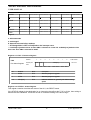
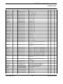
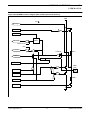
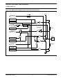
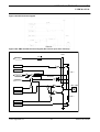
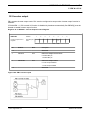
1
[APG013-UM-100-EN] APG013 8-bit RISC Microcontroller User Manual Rev 1.0.0 May 2011 AppoTech Limited Add: Unit 705-707, 7/F, IC Development Ctr, No. 6, Science Park West Ave. Hong Kong Science Park, Shatin, N.T. HK Tel: (852) 2607 4090 Fax: (852) 2607 4096 www.appotech.com APG013 8-bit RISC Microcontroller CPU • • 8-bit RISC CPU core Maximum 7.5 MIPS Instruction Set • • • 43 instructions Most instructions need 1 system clocks to execute Branch instructions need 1 or 2 system clocks to execute Memory • • • 64-byte SRAM 1K x 13-bit internal OTP program memory 10-byte user ID Watchdog Timer (WDT) • • • Oscillation Sources • • • • • • • • 5 hardware interrupt sources 1 software interrupt instruction 5 level hardware stacks • • 5 programmable digital I/O, 1 input port Programmable internal weak pull-up resistor Programmable internal weak pull-down resistor Programmable open-drain output Timer0 • • • • • One general purpose 8-bit timer Timer mode Counter mode PWM mode 8-bit programmable prescaler Reset at 2V or 2.4V Low Voltage Detector (LVD) • • • I/O Ports • • External RC oscillator (ERC) High Frequency Crystal/Resonator Oscillator (HF) Crystal/Resonator Oscillator (XT) Internal RC Oscillator (IRC) External Resistor/ Internal Capacitor Oscillator (ERIC) Power-on Reset (POR) • Interrupt Sources CLRWDT instruction to clear WDT counter Programmable postscaler Programmable overflow timer System Reset Voltage monitor Programmable voltage detection/indication levels: 1.8V/2.2V/2.4V/2.7V Operating Temperature Range • -40℃ to 85℃ Operating Voltage Range • • 2.2V to 3.6V at 1 MIPS 3.3V to 3.6V at 4 MIPS Package Type • • 8-pin DIP/SOP DIE form Timer1 • • • One general purpose 8/16-bit timer Timer mode Cascade mode AppoTech Limited Address Centre, :Unit 705-707, 7/F, IC Development No.6, Science Park West Ave., Hong Kong Science Park, Shatin, N.T., Hong Kong Telephone :(852) 2607 4090 Fax :(852) 2607 4096 www.appotech.com Rev 1.0.0 APG013 8-bit RISC Microcontroller USER MANUAL Table of Contents Chapter 1 Architecture Overview ........................................................................................6 1.1.Hardware architecture.................................................................................................6 1.2.Pin assignment............................................................................................................ 6 1.3.Pin description............................................................................................................. 6 Chapter 2 Memory Organization .........................................................................................8 2.1.Program memory organization.....................................................................................8 2.2.ID space and Smart option..........................................................................................9 2.3.Product ID and Check sum words..............................................................................11 2.4.Data memory organization.........................................................................................12 Chapter 3 Instruction Set ...................................................................................................21 3.1.Instruction set summary.............................................................................................21 3.2.Instruction description................................................................................................24 Chapter 4 Power Up and Reset .........................................................................................39 4.1.Power-on Reset (POR) and Low Voltage Reset (LVR)..............................................43 4.2.RSTB and Watchdog Reset.......................................................................................45 Chapter 5 Clock and Power-saving Mode ........................................................................47 5.1.System clock source..................................................................................................47 5.1.1.Single Oscillator Mode......................................................................................47 5.1.2.Dual Oscillator Mode........................................................................................47 5.1.3.System Speed Selection...................................................................................48 5.2.Power saving mode...................................................................................................48 5.3.System clock output...................................................................................................51 Chapter 6 Interrupt .............................................................................................................52 6.1.External interrupt.......................................................................................................55 6.2.Timer0 interrupt......................................................................................................... 56 6.3.Timer1 interrupt......................................................................................................... 56 6.4.Port B input change interrupt.....................................................................................56 Chapter 7 Timer0 .................................................................................................................58 7.1.Timer mode................................................................................................................62 7.2.Counter mode............................................................................................................62 7.3.PWM mode................................................................................................................ 63 7.4.Scaler........................................................................................................................ 65 Chapter 8 Timer1 .................................................................................................................66 8.1.Timer mode................................................................................................................70 © 2011 AppoTech Ltd 3 APG013-UM-100-EN Rev 1.0.0 APG013 8-bit RISC Microcontroller USER MANUAL 8.2.Cascade mode...........................................................................................................70 Chapter 9 Watchdog ...........................................................................................................71 Chapter 10 IO Port ..............................................................................................................72 10.1.Normal I/O port function...........................................................................................72 10.1.1.Port B.............................................................................................................72 10.2.Inverter output..........................................................................................................84 Chapter 11 Electrical Characteristics ...............................................................................85 11.1.Absolute maximum ratings*.....................................................................................85 11.2.DC Characteristics...................................................................................................86 11.3.Data Retention Characteristics in SLEEP Mode.......................................................87 11.4.AC Characteristics...................................................................................................87 11.5.Oscillator Characteristics.........................................................................................88 11.6.Reset Characteristics...............................................................................................89 Chapter 12 Package Dimensions ......................................................................................92 12.1.8-pin DIP..................................................................................................................92 12.2.8-pin SOP................................................................................................................ 93 Appendix I Revision History ...........................................................................................94 APG013-UM-100-EN 4 © 2011 AppoTech Ltd Rev 1.0.0 APG013 8-bit RISC Microcontroller USER MANUAL Table of Registers Register 2-1: FSR – File Select Register..........................................................................................18 Register 2-2: STATUS – Status Register..........................................................................................18 Register 2-3: PCL – PC Low Byte Register......................................................................................20 Register 4-1: PCON1 – Power Control 1 Register............................................................................40 Register 4-2: PCON2 – Power Control 2 Register............................................................................42 Register 4-3: CLKCON – Clock Control Register.............................................................................44 Register 6-1: INTEN – Interrupt Mask Register................................................................................54 Register 6-2: INTF – Interrupt Status Register.................................................................................56 Register 7-1: T0CNT – Timer0 Counter Register..............................................................................59 Register 7-2: T0PR – Timer0 Period Register..................................................................................59 Register 7-3: T0DUTY – Timer0 PWM Mode Duty Width Register...................................................59 Register 7-4: T0CON – Timer0 Control Register..............................................................................60 Register 8-1: T1CNT – Timer1 Counter Register..............................................................................67 Register 8-2: T1PR – Timer1 Period Register..................................................................................67 Register 8-3: T1CON – Timer1 Control Register..............................................................................68 Register 10-1: PBDIR – Port B Direction Control Register...............................................................72 Register 10-2: PBDATA – Port B Pin Data Register..........................................................................73 Register 10-3: PBWAK – Port B Pin Interrupt/Wake-up Control Register.........................................73 Register 10-4: ODCON – Open-drain Output Control Register........................................................74 Register 10-5: PUPCON – Internal Weak Pull-up Control Register..................................................75 Register 10-6: PDNCON – Internal Weak Pull-down Control Register.............................................76 Register 10-7: INVCON – Inverter Output Control Register..............................................................81 © 2011 AppoTech Ltd 5 APG013-UM-100-EN Rev 1.0.0 APG013 8-bit RISC Microcontroller USER MANUAL Chapter 1 Architecture Overview 1.1. Hardware architecture OSC PORTB 8-bitRISC RISCAPG012A APG013 CPU 8-bit CPU CORE POR/LVD WDT TIMER0 TIMER1 1K x 13bit OTP 64 byte SRAM 1.2. Pin assignment Figure 1-1: APG013 8-pin DIP / SOP package VDD 1 PB5 / XIN 2 PB4 / XOUT 3 PB3 / RSTB 4 APG013-UM-100-EN APG013 APG012A 8-pin 6 8 VSS 7 PB0 / INT0B 6 PB1 / INT1B 5 PB2 / T0CK / T0PWM © 2011 AppoTech Ltd Rev 1.0.0 APG013 8-bit RISC Microcontroller USER MANUAL 1.3. Pin description Table 1-1: APG013 pin description Name Pin # 8-pin Direction Function PB0/INT0B 7 I/O Bidirectional input/output port System wakeup Configurable weak pull-down resistor Configurable weak pull-up resistor Configurable open-drain output External interrupt input PB1/INT1B 6 I/O Bidirectional input/output port System wakeup Configurable weak pull-down resistor Configurable weak pull-up resistor Configurable open-drain output External interrupt input PB2/T0CK/T0PWM 5 I/O Bidirectional input/output port System wakeup Configurable weak pull-down resistor Configurable weak pull-up resistor Configurable open-drain output Timer0 external clock input Timer0 PWM output PB3/RSTB 4 I Input only port System wakeup System reset PB4/XOUT 3 I/O Bidirectional input/output port System wakeup System clock output Configurable weak pull-up resistor Configurable open-drain output XOSC clock output © 2011 AppoTech Ltd 7 APG013-UM-100-EN Rev 1.0.0 APG013 8-bit RISC Microcontroller USER MANUAL PB5/XIN 2 I/O Bidirectional input/output port System wakeup Configurable weak pull-up resistor Configurable open-drain output External clock input XOSC clock input VDD 1 Power Positive power supply VSS 8 Ground Negative power supply. Ground. APG013-UM-100-EN 8 © 2011 AppoTech Ltd Rev 1.0.0 APG013 8-bit RISC Microcontroller USER MANUAL Chapter 2 Memory Organization 2.1. Program memory organization APG013 has a 10-bit program counter (PC) capable of addressing 1K x 13-bit program memory space. The address range is 0x000 to 0x3FF. There is an extra ID space for smart options and user region. Smart options range from 0x0 to 0x1. The address from 0x2 to 0x5 is reserved. The address from0x6 to 0xF is user ID region. The reset vector is 0x000. PC stack over vector is 0x003. Hardware interrupt vector is 0x008. Figure 2-1: APG013 program memory space Program Space 10-bit PC Reset Vector 0x000 ... PC stack 0 Stack over Vector PC stack 1 0x003 ... PC stack 2 H/W interrupt Vector PC stack 3 0x008 PC stack 4 ID Space Smart option 0 0x0 Smart option 1 0x1 0x2 Reserved ... 0x5 0x6 User ID region 0x3FF 0xF © 2011 AppoTech Ltd 9 APG013-UM-100-EN Rev 1.0.0 APG013 8-bit RISC Microcontroller USER MANUAL 2.2. ID space and Smart option Smart option is used to define the starting condition of the APG013. The reserved bits of smart option must be kept 1. Smart option 0 12 11 Reserved Smart option 1 12 11 Reserved 10 Reserved 10 9 8 7 6 PB4CLKO PCHSEL LVD_SEL PORSEL 9 8 WDTCEN 7 CLKDIV 6 5 4 5 4 Reserved RCSEL 3 2 1 0 WDTSEL RDPORT RSTBEN 3 2 1 0 CLKSEL Table 2-1: Smart option 0 description Name Description RSTBEN RSTB pin enable 1: Set PB3 as normal input pin 0: Set PB3 as reset pin RDPORT Port read selection (Valid when the pad is configured as output pin) 1: Read output register 0: Read pad WDTSEL Watchdog reset select 0: WDT will not reset the system after 1st wake up from SLEEP mode but will set the WDTFLAG in the CLKCON. If this bit is not cleared after 2nd wake up from SLEEP, WDT will reset the system. WDTFLAG can be cleared by SLEEP, IDLE or CLRWDT instruction. (Notes: With this setting WDT will not reset the system after 1st wakeup from IDLE mode too. But the WDTFLAG in CLKCON will not be set. If one want to enter IDLE mode again after 1st wake up from IDLE mode by WDT, CLRWDT instruction must be executed first!) 1: WDT will always reset the system after wake up from SLEEP mode. PORSEL Power up delay time select = 0111: Power-on delay time is 2.25 ms. SLEEP mode wake-up delay time is 2.25 ms = 1111: Power-on delay time is 4.5 ms. SLEEP mode wake-up delay time is 4.5 ms = x110: Power-on delay time is 18 ms. SLEEP mode wake-up delay time is 18 ms = x101: Power-on delay time is 72 ms. SLEEP mode wake-up delay time is 72 ms = x100: Power-on delay time is 288 ms. SLEEP mode wake-up delay time is 288 ms = 0011: Power-on delay time is 2.25 ms. SLEEP mode wake-up delay time is 17.5us(1) = 1011: Power-on delay time is 4.5 ms. SLEEP mode wake-up delay time is 17.5us(1) = x010: Power-on delay time is 18 ms. SLEEP mode wake-up delay time is 17.5 us(1) = x001: Power-on delay time is 72 ms. SLEEP mode wake-up delay time is 17.5 us(1) = x000: Power-on delay time is 288 ms. SLEEP mode wake-up delay time is 17.5 us(1) LVD_SEL LVD select APG013-UM-100-EN 10 © 2011 AppoTech Ltd Rev 1.0.0 APG013 8-bit RISC Microcontroller USER MANUAL 0: LVD will reset chip if VDD is below 2.2V LVD2 flag is not valid. LVD3 will set 1 to indicate VDD < 2.4V LVD4 will set 1 to indicate VDD < 2.7V The system will release from reset if VDD is above 2.3V. 1: LVD will reset chip if VDD is below 1.8V LVD2 will set 1 to indicate VDD < 2.2V LVD3 will set 1 to indicate VDD < 2.4V LVD4 will set 1 to indicate VDD < 2.7V The system will release from reset if VDD is above 1.9V. PCHSEL PC[9:8] select 1: PC[9:8] will remained unchanged when executing any instructions related to PC. 0: PC[9:8] will clear to zero when executing any instructions related to PC. PB4CLKO PB4/XOUT pin select 1: PB4 is selected to output RC oscillator clock after power up 0: PB4 is selected for IO, output RC oscillator or divider clock. (Please refer to Section 5.3. System clock output for detailed descriptions on the settings.) Table 2-2: Smart option 1 description Name Description CLKSEL Oscillator selection =111: IRC =110: ERC =101: XOSC (100KHz to 1MHz) =100: XOSC (1MHz to 10MHz) =011: XOSC (10MHz to 16MHz) =010 : XOSC (32KHz) =001 : Invalid =000 : Dual Oscillator Mode: IRC + 32kHz XOSC (Both IRC & 32KHz XOSC could be selected as system clock) RCSEL Internal RC oscillator frequency selection =11: 8MHz =10: 4MHz =01: 1MHz =00: 455KHz WDTCEN WDT enable 1010: WDT disable © 2011 AppoTech Ltd 11 APG013-UM-100-EN Rev 1.0.0 APG013 8-bit RISC Microcontroller USER MANUAL Others: WDT enable CLKDIV V System clock division 11: divide 1 10: divide 2 01: divide 4 00: divide 8 Note: 1. When the clock runs slower than WDT, the timer-out period will probably be longer than 17.5us. The magnitude of discrepancy depends on frequency difference between the clock and WDT. 2.3. Product ID and Check sum words User information like product ID or check sum words can be stored in User region. This information can be read out by APG013 programmer or RETW command at customer firmware. Before RETW is called, user should first set READ_SMART (PCON2.7) and use the CALL instruction to jump to the location in the User region. Then use RETW instruction to return a byte in the User region. Only the User region (0x6 – 0xF) can be accessed. The addresses 0x0 to 0x5 are reserved. READ_SMART bit will be cleared automatically after execution of RETW. Figure 2-2 shows the proper access method. Figure 2-2: Accessing product ID APG013-UM-100-EN 12 © 2011 AppoTech Ltd Rev 1.0.0 APG013 8-bit RISC Microcontroller USER MANUAL Program space ... ID Space 1. set Read _smart bit to 1 0x0 Smart option 0 0x1 Smart option 1 0x2 2. use CALL to jump to User region Reserved ... 0x3 3. use RETW to return a byte User region 0xF V Firmware code ... 4. Read_smart bit is automatically cleared after RETW Note: 1. Only RETW should be used to read the product ID. If instruction other than RETW is used, the execution sequence will jump to an unknown location. 2.4. Data memory organization APG013's memory bank is divided into two banks. Memory space from 0x00 to 0x2F can be accessed by Bank 0 and 0x30-0x3F can be accessed by both Bank 0 and Bank 1. 0x00 to 0x0F are reserved for SFR (Special Function Registers), while 0x10 to 0x2F are available as SRAM, most SFR in this location can be accessed by MOV instruction. Another part of SFR are stored in a separated location which can only accessed by the EXT instruction. Data memory space start from 0x30 to 0x3F are separated into two banks: bank 0 and bank 1. Each bank provides 16 bytes of SRAM. Totally, there are 64 bytes of SRAM available for use. © 2011 AppoTech Ltd 13 APG013-UM-100-EN Rev 1.0.0 APG013 8-bit RISC Microcontroller USER MANUAL Figure 2-3: APG013 Data Memory Map APG012A Map APG013 Memory Memory Map Accessed by EXT 0x00 SFR 0x0F Accessed by MOV 0x00 16 Bytes SFR 0x0F 0x10 16 Bytes 32 Bytes SRAM 0x2F Bank 0/ Bank 1 Bank 0 Bank 1 0x30 SRAM 0x3F 16 Bytes 0x30 SRAM 16 Bytes 0x3F APG013 data memory space is partitioned into two parts, SFR(Special Function Registers) and SRAM. SFR is special registers reserved for CPU core and peripheral usage. It is divided into general part and extend part. The general part can be accessed either directly or indirectly through the File Select Register (FSR). The extend part can only be accessed by EXT instruction. The Special Function Registers are used by CPU core and peripherals for controlling the desired operation of the device. The Special Function Registers can be classified into two sets (CPU core and peripheral). Those registers associated with the “CPU core” functions are described in this section, and those related to the operation of the peripheral features are described in the section of that peripheral feature. SRAM can be used as data storage for user program. APG013-UM-100-EN 14 © 2011 AppoTech Ltd Rev 1.0.0 APG013 8-bit RISC Microcontroller USER MANUAL Table 2-3: APG013 data memory space Address General Part Extend part 0x00 INDF CLKCON 0x01 T0CNT T0CON 0x02 PCL T1CON 0x03 STATUS INVCON 0x04 FSR PCON2 0x05 - - 0x06 PBDATA PBDIR 0x07 T1CNT - 0x08 PCON1 - 0x09 PBWAK - 0x0A T1PR - 0x0B PDNCON - 0x0C ODCON T0DUTY 0x0D PUPCON T0PR 0x0E INTEN - 0x0F INTF - 0x10 - 0x11 SRAM … - 0x3F - Table 2-4: Table 2-6: APG013 Register Table Register Address Bit7 Bit6 Bit5 Bit4 INDF 0x00 Indirect addressing to general part data memory T0CNT 0x01 Timer0 counter PCL 0x02 PC low byte STATUS 0x03 RST © 2011 AppoTech Ltd T1_IDX GPR0 15 TO_ Bit3 PD_ Bit2 Z Bit1 DC Bit0 C APG013-UM-100-EN Rev 1.0.0 APG013 8-bit RISC Microcontroller USER MANUAL FSR 0x04 GPR3 GPR2 INDA[5:0] - 0x05 - PBDATA 0x06 Port B Pin Data Register T1CNT 0x07 8/16-bit Timer1 counter PCON1 0x08 WDTEN[3] EIS BANKRE G - - - INTEDG1 INTEDG0 PBWAK 0x09 - - PBWAK5 PBWAK4 PBWAK3 PBWAK2 PBWAK1 PBWAK0 T1PR 0x0A 8/16-bit Timer1 period width PDNCON 0x0B GPR4 PBPDN2 PBPDN1 PBPDN0 - - - - ODCON 0x0C - - PBOD5 PBOD4 GPR5 PBOD2 PBOD1 PBOD0 PUPCON 0x0D - - PBPUP5 PBPUP4 GPR6 PBPUP2 PBPUP1 PBPUP0 INTEN 0x0E GIE GPR7 T1IE - INT1IE INT0IE PBIE T0IE INTF 0x0F - - T1IF - INT1IF INT0IF PBIF T0IF CLKCON EXT 0x00 - LVD4 LVD3 LVD2 WDTFLA G SPEED COUTSEL[1:0] T0CON EXT 0x01 T0MODE T0EN T0CS T0SE PSA PS[2:0] T1CON EXT 0x02 - T1EN - - T1SIZE T1CS1 INVCON EXT 0x03 - - - - PB1INVS PB1INVE N PCON2 EXT 0x04 READ_SMART PWRSAV E SCLKSEL[1:0] - WDTEN[2:0] - EXT 0x05 - - - - - - - - PBDIR EXT 0x06 - - PBDIR5 PBDIR4 - PBDIR2 PBDIR1 PBDIR0 - EXT 0x07 - - - - - - - - - EXT 0x08 - - - - - - - - - EXT 0x09 - - EXT 0x0A - - EXT 0x0B - T0DUTY EXT 0x0C Timer0 PWM duty width T0PR EXT 0x0D Timer0 PWM period width - EXT 0x0E - - EXT 0x0F - CLKSRC[1:0] - -: undefined APG013-UM-100-EN 16 © 2011 AppoTech Ltd Rev 1.0.0 APG013 8-bit RISC Microcontroller USER MANUAL Note: Reading to undefined space will return 0. Writing to undefined space will result in nothing. GPRx stands for General Purpose Register Special function registers reset status is listed below. Table 2-7: Special function registers reset value Register Power-on reset LVR reset WDT reset W xxxx-xxxx uuuu-uuuu uuuu-uuuu uuuu-uuuu uuuu-uuuu uuuu-uuuu INDF xxxx-xxxx xxxx-xxxx xxxx-xxxx xxxx-xxxx uuuu-uuuu uuuu-uuuu T0CNT 0000-0000 0000-0000 0000-0000 0000-0000 uuuu-uuuu dddd-dddd PCL 0000-0000 0000-0000 0000-0000 0000-0000 uuuu-uuuu uuuu-uuuu STATUS 0001-1xxx 000u-uuuu 0000-uuuu 000u-uuuu uuuu-uuuu uuuu-uuuu FSR xxxx-xxxx uuuu-uuuu uuuu-uuuu uuuu-uuuu uuuu-uuuu uuuu-uuuu - - - - - - - PBDATA xxxx-xxxx uuuu-uuuu uuuu-uuuu uuuu-uuuu dddd-dddd dddd-dddd T1CNT xxxx-xxxx uuuu-uuuu uuuu-uuuu uuuu-uuuu uuuu-uuuu dddd-dddd PCON1 10xx-0x00 10xx-0x00 10xx-0x00 10xx-0x00 uuuu-uuuu uuuu-uuuu PBWAK 0000-0000 0000-0000 0000-0000 0000-0000 uuuu-uuuu uuuu-uuuu T1PR 1111-1111 1111-1111 1111-1111 1111-1111 uuuu-uuuu uuuu-uuuu PDNCON 1111-1111 1111-1111 1111-1111 1111-1111 uuuu-uuuu uuuu-uuuu ODCON 0000-0000 0000-0000 0000-0000 0000-0000 uuuu-uuuu uuuu-uuuu PUPCON 1111-1111 1111-1111 1111-1111 1111-1111 uuuu-uuuu uuuu-uuuu INTEN 0000-0000 0000-0000 0000-0000 0000-0000 uuuu-uuuu uuuu-uuuu INTF 0000-0000 0000-0000 0000-0000 0000-0000 uuuu-uuuu* uuuu-uuuu* CLKCON x000-0000** x000-0000** x000-0000** x000-0000** uuuu-uuuu uuuu-uuuu T0CON 0111-1111 0111-1111 0111-1111 0111-1111 uuuu-uuuu uuuu-uuuu T1CON 00xx-0x00 00xx-0x00 00xx-0x00 00xx-0x00 uuuu-uuuu uuuu-uuuu INVCON xx00-0000 xx00-0000 xx00-0000 xx00-0000 uuuu-uuuu uuuu-uuuu © 2011 AppoTech Ltd 17 RSTB reset SLEEP Wakeup IDLE Wakeup APG013-UM-100-EN Rev 1.0.0 APG013 8-bit RISC Microcontroller USER MANUAL PCON2 0000-x010 0000-x010 0000-x010 0000-x010 uuuu-uuuu uuuu-uuuu - - - - - - - PBDIR 1111-1111 1111-1111 1111-1111 1111-1111 uuuu-uuuu uuuu-uuuu - 0000-0000 0000-0000 0000-0000 0000-0000 uuuu-uuuu uuuu-uuuu - - - - - - - T0DUTY xxxx-xxxx uuuu-uuuu uuuu-uuuu uuuu-uuuu uuuu-uuuu uuuu-uuuu T0PR 1111-1111 1111-1111 1111-1111 1111-1111 uuuu-uuuu uuuu-uuuu Legend: x: unknown state u: unchanged d: depends on state before wakeup * : Unchanged bits in INTF will depend on the interrupt event. **: CLKCON[1:0] default will be 00 when PB4 is selected as normal I/O. CLKCON[1:0] default will be don't care when PB4 is selected for XOUT. Register 2-1: FSR – File Select Register FSR Address 7 File Select Register General part 0x04 6 5 4 GPR3 GPR2 R/W R/W 3 2 1 0 INDA[5:0] R/W R/W R/W R/W POR Default xxxx-xxxx R/W R/W Bit Bit Name Mode Description 7 GPR3 R/W General purpose register 6 GPR2 R/W General purpose register 5:0 INDA[5:0] R/W Indirect address to general part data memory space Register 2-2: STATUS – Status Register This register contains the arithmetic status of the ALU, the RESET status. If the STATUS register is the destination for an instruction that affects the Z, DC or C bits, then writing to these three bits is disabled. These bits are set or cleared according to the device logic. APG013-UM-100-EN 18 © 2011 AppoTech Ltd Rev 1.0.0 APG013 8-bit RISC Microcontroller USER MANUAL STATUS Address 7 Status Register General part 0x03 RST R/W 6 5 T1_ID GPR0 X R/W 4 3 2 1 0 POR Default TO_ PD_ Z DC C 0001-1xxx RO RO R/W R/W R/W R/W Bit Bit Name Mode Description 7 RST R/W Wake-up type selection bit 1: Wake-up from SLEEP on Port B input change. 0: Wake-up from other reset types. 6 T1_IDX R/W Timer1 index An index of T1CNT and T1PR write, in 16-bit mode, T1_IDX will be automatically toggled to MSB/LSB after writing to LSB/MSB. The counter will be updated after writing MSB. Writing will only be correct if LSB is read/written first and then MSB. (Refer to Chapter Timer 1) 5 GPR0 R/W General purpose register 4 TO_ RO Time out flag 1: Set after power-on or by the CLRWDT or SLEEP or IDLE instruction. 0: a watchdog time out occurred. 3 PD_ RO Power down flag 1: Set after power-on or by the CLRWDT instruction. 0: Clear by the SLEEP or IDLE instruction. 2 Z R/W Zero bit 1: The result of a logic operation is zero 0: The result of a logic operation is not zero © 2011 AppoTech Ltd 19 APG013-UM-100-EN Rev 1.0.0 APG013 8-bit RISC Microcontroller USER MANUAL 1 DC R/W Half carry/half borrow bit After addition operation 1: A carry from 4th low order bit of the result occurred. th 1:A carry from the 4 low order bit of the result occurred. th 0: A carry from the 4 low order bit of the result did not occur. After subtraction operation th 1: A borrow from the 4 low order bit of the result did not occur th 0: A borrow from the 4 low order bit of the result occurred 0 C R/W Carry/borrow bit After addition operation 1: A carry occurred. 0: A carry did not occur. After subtraction operation 1: A borrow did not occur 0: A borrow occurred After rotate operation, C contains the shifted out bit. Register 2-3: PCL – PC Low Byte Register APG013 has a 10-bit wide Program Counter (PC) and five levels hardware push/pop PC stack. The low byte of PC is called PCL. PC [9:8] bits are not directly readable or writable. As a program instruction is executed, the PC will contain the address of the next program instruction to be executed. The PC value is increased by one, every instruction cycle, unless an instruction changes PC. For a JMP instruction, the new PC value is provided by the JMP instruction word. For a CALL instruction, PC + 1 will be pushed into the Top of PC STACK (TOS). The new PC value is provided by the CALL instruction word. For interrupt condition, PC + 1 will be pushed into the Top of STACK (TOS). The new PC value is provided by interrupt vector. For a RET, RETI or RETW instruction, the new PC value is popped from TOS. If a RET, RETI or RETW executed after all data in PC STACK have been popped out, PC will be forced to stack over vector 0x003. For any instruction where the PCL is the destination, PC [7:0] is provided by the instruction word or ALU result. And PC [9:8] is either remain unchanged or clear to zeros that depends on the smart option PCHSEL. These instructions need 2 system clock cycles to execute. APG013-UM-100-EN 20 © 2011 AppoTech Ltd Rev 1.0.0 APG013 8-bit RISC Microcontroller USER MANUAL When PCON2 bit 7 READ_SMART is set to 1, it can use the CALL instruction to jump to the location in the user region and use RETW instruction to return a byte. This bit will be cleared automatically after execution of RETW. PCL Address 7 PC Low Byte Register General part 0x02 6 5 4 3 2 1 0 PCL R/W R/W R/W R/W Bit Bit Name Mode Description 7:0 PCL R/W PC low byte R/W POR Default 0000-0000 R/W R/W R/W Note: 1. Any instruction which write to PCL will need 2 system clock cycles to execute. 2. PCL cannot be used as the operator of IJZ or DJZ instruction. © 2011 AppoTech Ltd 21 APG013-UM-100-EN Rev 1.0.0 APG013 8-bit RISC Microcontroller USER MANUAL Chapter 3 Instruction Set 3.1. Instruction set summary Each APG013 instruction is a 13-bit word. Most instruction needs only 1 system clock (Fsys) cycle. Some branch instruction need 2 Fsys cycles. The APG013 instruction set symbols description is shown in Table 3-1. The APG013 instruction set is summarized in Table 3-2. For byte-oriented instructions, ‘R’ represents a general part data memory designator. The ‘R’ specifies which data memory byte is to be used by the instruction. ‘ER’ represents an extend part data memory designator. For bit-oriented instructions, ’b’ represents a bit field designator which selects the number of the bit affected by the operation. For literal and control operations, ’k’ represents an eight or ten bit constant or literal value. Table 3-1: APG013 instruction set symbols description Symbol Description R General part data memory address ER Extend part data memory address W Working register b Bit address k Literal field [] Register bit field => Assign to Table 3-2: APG013 instruction set Mnemonic Cycles Opcode NOP 1 0-0000-0000-0000 DAA 1 0-0000-0000-0001 SLEEP 1 0-0000-0000-0011 IDLE 1 0-0000-0000-1000 CLRWDT 1 0-0000-0000-0100 RET 2 0-0000-0001-0010 RETI 2 0-0000-0001-0011 SINT k 2 0-0000-0001-01kk EXT W, ER 1 0-0000-0010-rrrr EXT ER, W 1 0-0000-0011-rrrr MOV R, W 1 0-0000-01rr-rrrr CLRW 1 0-0000-1000-0000 APG013-UM-100-EN Description No operation Decimal Adjust after addition Enter SLEEP mode. 0 => WDTCNT Enter IDLE mode. 0 => WDTCNT 0 => WDTCNT [TOS] => PC [TOS] => PC, 1 => GIE PC => [TOS], K => PC, 0 => GIE ER => W W => ER W => R 0 => W 22 Z * DC - C * - © 2011 AppoTech Ltd Rev 1.0.0 APG013 8-bit RISC Microcontroller USER MANUAL CLR R SBCW R, W SBCR R, W SUBW R, W SUBR R, W DEC W, R DEC R OR W, R OR R, W AND W, R AND R, W XOR W, R XOR R, W ADD W, R ADD R, W MOV W, R TEST R COM W, R COM R INC W,R INC R DJZ W, R 1 1 1 1 1 1 1 1 1 1 1 1 1 1 1 1 1 1 1 1 1 1/2 0-0000-11rr-rrrr 1-1110-10rr-rrrr 1-1110-11rr-rrrr 0-0001-00rr-rrrr 0-0001-01rr-rrrr 0-0001-10rr-rrrr 0-0001-11rr-rrrr 0-0010-00rr-rrrr 0-0010-01rr-rrrr 0-0010-10rr-rrrr 0-0010-11rr-rrrr 0-0011-00rr-rrrr 0-0011-01rr-rrrr 0-0011-10rr-rrrr 0-0011-11rr-rrrr 0-0100-00rr-rrrr 0-0100-01rr-rrrr 0-0100-10rr-rrrr 0-0100-11rr-rrrr 0-0101-00rr-rrrr 0-0101-01rr-rrrr 0-0101-10rr-rrrr DJZ R 1/2 0-0101-11rr-rrrr RRC W, R RRC R RLC W, R RLC R SWAP W, R SWAP R IJZ W, R 1 1 1 1 1 1 1/2 0-0110-00rr-rrrr 0-0110-01rr-rrrr 0-0110-10rr-rrrr 0-0110-11rr-rrrr 0-0111-00rr-rrrr 0-0111-01rr-rrrr 0-0111-10rr-rrrr IJZ R 1/2 0-0111-11rr-rrrr BC R, b BS R, b JBC R, b JBS R, b CALL k JMP k MOVW k ORW k ANDW k 1 1 1/2 1/2 2 2 1 1 1 0-100b-bbrr-rrrr 0-101b-bbrr-rrrr 0-110b-bbrr-rrrr 0-111b-bbrr-rrrr 1-00kk-kkkk-kkkk 1-01kk-kkkk-kkkk 1-1000-kkkk-kkkk 1-1001-kkkk-kkkk 1-1010-kkkk-kkkk © 2011 AppoTech Ltd 0 => R R + (~W) => W R + (~W) => R R – W => W R – W => R R – 1 => W R – 1 => R W | R => W W | R => R W & R => W W & R => R W ^ R => W W ^ R => R W + R => W W + R => R R => W R => R ~R => W ~R => R R + 1 => W R + 1 => R R – 1 => W, skip next instruction if result = 0 R – 1 => R, skip next instruction if result = 0 R[7:1] => W[6:0], C => W[7], R[0] => C R[7:1] => R[6:0], C => R[7], R[0] => C R[6:0] => W[7:1], C => W[0], R[7] => C R[6:0] => R[7:1], C => R[0], R[7] => C R[3:0] => W[7:4], R[7:4] => W[3:0] R[3:0] => R[7:4], R[7:4] => R[3:0] R + 1 => W, skip next instruction if result = 0 R + 1 => R, skip next instruction if result = 0 0 => R[b] 1 => R[b] Skip next instruction if R[b] = 0 Skip next instruction if R[b] = 1 PC => [TOS], K => PC K => PC K => W K | W => W K & W => W 23 * * * * * * * * * * * * * * * * * * * * - * * * * * * - * * * * * * - - - - - - * * * * - - - - * * - - APG013-UM-100-EN Rev 1.0.0 APG013 8-bit RISC Microcontroller USER MANUAL XORW k RETW k SUBK k ADC W, R ADC R, W ADDW k 1 2 1 1 1 1 1-1011-kkkk-kkkk 1-1100-kkkk-kkkk 1-1101-kkkk-kkkk 1-1110-00rr-rrrr 1-1110-01rr-rrrr 1-1111-kkkk-kkkk K ^ W => W K => W, [TOS] => PC K – W => W R + W + C => W R + W + C => R K + W => W * * * * * * * * * * * * * * : affected flag – : unaffected flag APG013-UM-100-EN 24 © 2011 AppoTech Ltd Rev 1.0.0 APG013 8-bit RISC Microcontroller USER MANUAL 3.2. Instruction description ADC W, R Add W and R with Carry Operands: 0 ≤ R ≤ 0x3F Operation: W + R + C => W Status Affected: C, DC, Z Description: Add the contents of the W register and register ‘R’ with Carry. The result is stored in the W register. Cycles: 1 ADC R, W Add W and R with Carry Operands: 0 ≤ R ≤ 0x3F Operation: W + R + C => R Status Affected: C, DC, Z Description: Add the contents of the W register and register ‘R’ with Carry. The result is stored in the ‘R’ register. Cycles: 1 ADD W, R Add W and R Operands: 0 ≤ R ≤ 0x3F Operation: W + R => W Status Affected: C, DC, Z Description: Add the contents of the W register and register ‘R’. The result is stored in the W register. Cycles: 1 ADD R, W Add W and R Operands: 0 ≤ R ≤ 0x3F Operation: W + R => R Status Affected: C, DC, Z Description: Add the contents of the W register and register ‘R’. The result is stored in the ‘R’ register. Cycles: 1 © 2011 AppoTech Ltd 25 APG013-UM-100-EN Rev 1.0.0 APG013 8-bit RISC Microcontroller USER MANUAL ADDW k Add W and Immediate Operands: 0 ≤ k ≤ 0xFF Operation: W + k => W Status Affected: C, DC, Z Description: Add the contents of the W register with the 8-bit immediate “k”. The result is stored in the W register. Cycles: 1 AND W, R AND W and R Operands: 0 ≤ R ≤ 0x3F Operation: W and R => W Status Affected: Z Description: The contents of the W register are AND’ed with register ‘R’. The result is stored in the W register. Cycles: 1 AND R, W AND W and R Operands: 0 ≤ R ≤ 0x3F Operation: W and R => R Status Affected: Z Description: The contents of the W register are AND’ed with register ‘R’. The result is stored in the ‘R’ register. Cycles: 1 ANDW k AND immediate with W Operands: 0 ≤ k ≤ 0xFF Operation: W AND k => W Status Affected: Z Description: The contents of the W register are AND’ed with 8-bit immediate “k”. The result is stored in the W register. Cycles: 1 APG013-UM-100-EN 26 © 2011 AppoTech Ltd Rev 1.0.0 APG013 8-bit RISC Microcontroller USER MANUAL BC R, b Operands: Clear bit in R 0 ≤ R ≤ 0x3F 0≤b≤7 Operation: 0 => R[b] Status Affected: None Description: Clear bit ‘b’ in register ‘R’. Cycles: 1 BS R, b Operands: Set Bit in R 0 ≤ R ≤ 0x3F 0≤b≤7 Operation: 1 => R[b] Status Affected: None Description: Set bit ‘b’ in register ‘R’ Cycles: 1 CALL k Subroutine call Operands: 0 ≤ k ≤ 0x3FF Operation: PC + 1 => TOP of Stack; k => PC Status Affected: None Description: Subroutine call. First, return address (PC + 1) is pushed onto the stack. The 10-bit immediate address is loaded into PC. Cycles: CLR 2 R Clear R Operands: 0 ≤ R ≤ 0x3F Operation: 0x00 => R; 1 => Z Status Affected: Z Description: The contents of register ‘R’ are cleared and the Z bit is set. Cycles: 1 © 2011 AppoTech Ltd 27 APG013-UM-100-EN Rev 1.0.0 APG013 8-bit RISC Microcontroller USER MANUAL CLRW Clear W Operands: None Operation: 0x00 => W; 1 => Z. Status Affected: Z Description: The contents of register W are cleared and the Z bit is set. Cycles: 1 CLRWDT Clear Watchdog timer Operands: None Operation: 0x00 => WDTCNT; 0x00 => WDT postscaler (if assigned); 1 => TO_; 1 => PD_; Status Affected: TO_, PD_. Description: The CLRWDT instruction resets the WDT. It also resets the postscaler, if the postscaler is assigned to the WDT. Status bits TO_ and PD_ are set. Cycles: 1 COM W, R Complement R Operands: 0 ≤ R ≤ 0x3F Operation: ~R => W Status Affected: Z Description: The contents of register ‘R’ are complemented. The result is stored in W register. Cycles: 1 COM R Complement R Operands: 0 ≤ R ≤ 0x3F Operation: ~R => R Status Affected: Z Description: The contents of register ‘R’ are complemented. The result is stored in ‘R’ register. Cycles: 1 APG013-UM-100-EN 28 © 2011 AppoTech Ltd Rev 1.0.0 APG013 8-bit RISC Microcontroller USER MANUAL DAA Adjust W’s data format from HEX to DEC (Addition) Operands: None Operation: W (HEX) => W (DEC) Status Affected: C Description: Convert the W data from hexadecimal to decimal formal after any addition operation and restored to W. Step 0: If DC = 1 or W[3:0] ≥ 0xA, W + 0x06 => W. Step 1: If C = 1 or W[7:4] ≥ 0xA, W + 0x60 => W, and 1 => C, if W + 0x60 > 0xFF. Cycles: DEC 1 W, R Decrement R Operands: 0 ≤ R ≤ 0x3F Operation: R – 1 => W Status Affected: Z Description: Decrement register ‘R’. The result is stored in the W register. Cycles: 1 DEC R Decrement R (placeholder) Operands: 0 ≤ R ≤ 0x3F Operation: R – 1 => R Status Affected: Z Description: Decrement register ‘R’. The result is stored in the ‘R’ register. Cycles: 1 DJZ W, R Decrement R, Skip if 0 Operands: 0 ≤ R ≤ 0x3F Operation: R – 1 => W; skip if result = 0. Status Affected: None Description: The contents of register ‘R’ are decremented. The result is stored in W register. If the result is 0, the next instruction, which is already fetched, is discarded and a NOP is executed instead making if a two cycle instruction. Cycles: © 2011 AppoTech Ltd 1 (2) 29 APG013-UM-100-EN Rev 1.0.0 APG013 8-bit RISC Microcontroller USER MANUAL DJZ R Decrement R, Skip if 0 Operands: 0 ≤ R ≤ 0x3F Operation: R – 1 => R; skip if result = 0. Status Affected: None Description: The contents of register ‘R’ are decremented. The result is stored in ‘R’ register. If the result is 0, the next instruction, which is already fetched, is discarded and a NOP is executed instead making if a two cycle instruction. Cycles: EXT 1 (2) W, ER Load the W register with ‘ER’ register in extend memory bank Operands: 0 ≤ ER ≤ 0xF Operation: ER => W Status Affected: None Description: Read the ‘ER’ register in extend memory bank to W register. Cycles: 1 EXT ER, W Load the ‘ER’ register in extend memory bank with W register Operands: 0 ≤ ER ≤ 0xF Operation: W => ER Status Affected: None Description: Load the ‘ER’ register in extend memory bank with W register Cycles: 1 IDLE Enter IDLE mode Operands: None Operation: 0x00 => WDTCNT; 0x00 => WDT postscaler (If assigned); 1 => TO_; 0 => PD_; Status Affected: TO_, PD_. Description: Time-out status bit (TO_) is set. The power-down status bit (PD_) is cleared. The WDTCNT and its postscaler are cleared. APG013 is put into IDLE mode. Cycles: APG013-UM-100-EN 1 30 © 2011 AppoTech Ltd Rev 1.0.0 APG013 8-bit RISC Microcontroller USER MANUAL IJZ W, R Increment R, Skip if 0 Operands: 0 ≤ R ≤ 0x3F Operation: R + 1 => W, skip if result = 0. Status Affected: None Description: The contents of register ‘R’ are incremented. The result is stored in W register. If the result is 0, then the next instruction, which is already fetched, is discarded and a NOP is executed making it a two-cycle instruction. Cycles: IJZ 1 (2) R Increment R, Skip if 0 Operands: 0 ≤ R ≤ 0x3F Operation: R + 1 => R, skip if result = 0. Status Affected: None Description: The contents of register ‘R’ are incremented. The result is stored in ‘R’ register. If the result is 0, then the next instruction, which is already fetched, is discarded and a NOP is executed making it a two-cycle instruction. Cycles: INC 1 (2) W, R Increment R Operands: 0 ≤ R ≤ 0x3F Operation: R + 1 => W Status Affected: Z Description: The contents of register ‘R’ are incremented. The result is stored in W register. Cycles: 1 INC R Increment R Operands: 0 ≤ R ≤ 0x3F Operation: R + 1 => R Status Affected: Z Description: The contents of register ‘R’ are incremented. The result is stored in ‘R’ register. Cycles: 1 © 2011 AppoTech Ltd 31 APG013-UM-100-EN Rev 1.0.0 APG013 8-bit RISC Microcontroller USER MANUAL JBC R, b Operands: Test bit in R, skip if clear 0 ≤ R ≤ 0x3F; 0≤b≤7 Operation: Skip if R[b] = 0 Status Affected: None Description: If bit ‘b’ in register ‘R’ is 0 then the next instruction is skipped. If bit ‘b’ in register ‘R’ is 0 then next instruction fetched during the current instruction execution is discarded, and a NOP is executed instead making this a 2-cycle instruction. Cycles: JBS 1 (2) R, b Operands: Test bit in R, skip if set 0 ≤ R ≤ 0x3F; 0≤b≤7 Operation: Skip if R[b] = 1 Status Affected: None Description: If bit ‘b’ in register ‘R’ is 1 then the next instruction is skipped. If bit ‘b’ in register ‘R’ is 1 then next instruction fetched during the current instruction execution is discarded, and a NOP is executed instead making this a 2-cycle instruction. Cycles: JMP 1 (2) k Unconditional Branch Operands: 0 ≤ k ≤ 0x3FF Operation: k => PC Status Affected: None Description: JMP is an unconditional branch. The 10-bit immediate value is loaded into PC. Cycles: 2 MOV R, W Load ‘R’ register with W register Operands: 0 ≤ R ≤ 0x3F APG013-UM-100-EN 32 © 2011 AppoTech Ltd Rev 1.0.0 APG013 8-bit RISC Microcontroller USER MANUAL Operation: W => R Status Affected: None Description: Load ‘R’ register with W register. Cycles: 1 MOV W, R Load W register with ‘R’ register Operands: 0 ≤ R ≤ 0x3F Operation: R => W Status Affected: None Description: Load W register with ‘R’ register. Cycles: 1 MOVW k Move immediate to W Operands: 0 ≤ k ≤ 0xFF Operation: k => W Status Affected: None Description: The 8-bit immediate ‘k’ is loaded into the W register. Cycles: 1 NOP No operation Operands: None Operation: No operation Status Affected: None Description: No operation Cycles: 1 OR W, R OR W with R Operands: 0 ≤ R ≤ 0x3F Operation: W or R => W Status Affected: Z Description: Inclusive OR the W register with register with register ‘R’. The result is stored in W register. © 2011 AppoTech Ltd 33 APG013-UM-100-EN Rev 1.0.0 APG013 8-bit RISC Microcontroller USER MANUAL Cycles: OR 1 R, W OR W with R Operands: 0 ≤ R ≤ 0x3F Operation: W or R => R Status Affected: Z Description: Inclusive OR the W register with register with register ‘R’. The result is stored in ‘R’ register. Cycles: 1 ORW k OR immediate with W Operands: 0 ≤ k ≤ 0xFF Operation: W OR k => W Status Affected: Z Description: Inclusive OR the W register with register with 8-bit immediate k. The result is stored in W register Cycles: 1 RET Return from Subroutine Operands: None Operation: TOP of Stack => PC Status Affected: None Description: The program counter is loaded from the top of the stack ( the return address). Cycles: 2 RETI Return from Interrupt, Set ‘GIE’ bit Operands: None Operation: TOP of Stack => PC 1 => GIE Status Affected: None Description: The program counter is loaded from the top of the stack (the return address). The APG013-UM-100-EN 34 © 2011 AppoTech Ltd Rev 1.0.0 APG013 8-bit RISC Microcontroller USER MANUAL ‘GIE’ bit is set to 1. Cycles: 2 RETW k Return with immediate in W Operands: 0 ≤ k ≤ 0xFF Operation: k => W Top of Stack => PC Status Affected: None Description: The W register is loaded with the 8-bit immediate ‘k’. The program counter is loaded from the top of the stack (the return address). Cycles: 2 RLC W, R Rotate left R through Carry Operands: 0 ≤ R ≤ 0x3F Operation: C => W[0]; R[7] => C; R[6:0] => W[7:1] Status Affected: C Description: The contents of register ‘R’ are rotate one bit to the left through the Carry flag. The result is stored in the W register. Cycles: 1 RLC R Rotate left R through Carry Operands: 0 ≤ R ≤ 0x3F Operation: C => R[0]; R[7] => C; R[6:0] => R[7:1] Status Affected: C Description: The contents of register ‘R’ are rotate one bit to the left through the Carry flag. The result is stored in the ‘R’ register. Cycles: 1 RRC W, R © 2011 AppoTech Ltd Rotate right R through Carry 35 APG013-UM-100-EN Rev 1.0.0 APG013 8-bit RISC Microcontroller USER MANUAL Operands: 0 ≤ R ≤ 0x3F Operation: C => W[7]; R[0] => C; R[7:1] => W[6:0] Status Affected: C Description: The contents of register ‘R’ are rotate one bit to the right through the Carry flag. The result is stored in the W register. Cycles: 1 RRC R Rotate right R through Carry Operands: 0 ≤ R ≤ 0x3F Operation: C => R[7]; R[0] => C; R[7:1] => R[6:0] Status Affected: C Description: The contents of register ‘R’ are rotate one bit to the right through the Carry flag. The result is stored in the ‘R’ register. Cycles: 1 SBCW R,W Subtract W from R with Carry Operands: 0 ≤ R ≤ 0x3F Operation: R+(~W)+C => W Status Affected: C, DC, Z Description: Subtract the data of the W register from the data of 'R' register with Carry. The result is stored in W register. Cycles: 1 SBCR R,W Subtract W from R with Carry Operands: 0 ≤ R ≤ 0x3F Operation: R+(~W)+C => R Status Affected: C, DC, Z Description: Subtract the data of the W register from the data of 'R' register with Carry. The result is stored in W register. Cycles: 1 APG013-UM-100-EN 36 © 2011 AppoTech Ltd Rev 1.0.0 APG013 8-bit RISC Microcontroller USER MANUAL SINT k Software interrupt Operands: 0 ≤ k ≤ 0x3 Operation: PC + 1 => Top of Stack; k => PC; 0 => GIE. Status Affected: None Description: Interrupt subroutine call. First, return address (PC + 1) is pushed onto the stack. The address k is loaded into PC. GIE is cleared. Cycles: 2 SLEEP Enter SLEEP mode Operands: None Operation: 0x00 => WDTCNT; 0x00 => WDT postscaler (If assigned); 1 => TO_; 0 => PD_; Status Affected: TO_, PD_. Description: Time-out status bit (TO_) is set. The power-down status bit (PD_) is cleared. The WDTCNT and its postscaler are cleared. The processor is put into SLEEP mode. Cycles: 1 SUBK k Subtract W from immediate Operands: 0 ≤ k ≤ 0xFF Operation: k – W => W Status Affected: C, DC, Z Description: Subtract the data of the W register from the 8-bit immediate ‘k’. The result is stored in W register. Cycles: 1 SUBR R, W Subtract W from R Operands: 0 ≤ R ≤ 0x3F Operation: R – W => R Status Affected: C, DC, Z Description: Subtract the data of the W register from the data of ‘R’ register. The result is © 2011 AppoTech Ltd 37 APG013-UM-100-EN Rev 1.0.0 APG013 8-bit RISC Microcontroller USER MANUAL stored in ‘R’ register. Cycles: 1 SUBW R, W Subtract W from R Operands: 0 ≤ R ≤ 0x3F Operation: R – W => W Status Affected: C, DC, Z Description: Subtract the data of the W register from the data of ‘R’ register. The result is stored in W register. Cycles: 1 SWAP W, R Swap nibbles in R Operands: 0 ≤ R ≤ 0x3F Operation: R[7:4] => W[3:0]; R[3:0] => W[7:4]; Status Affected: None Description: The upper and lower nibbles of register ‘R’ are exchanged. The result is stored in W register. Cycles: 1 SWAP R Swap nibbles in R Operands: 0 ≤ R ≤ 0x3F Operation: R[7:4] => R[3:0]; R[3:0] => R[7:4]; Status Affected: None Description: The upper and lower nibbles of register ‘R’ are exchanged. The result is stored in R register. Cycles: 1 TEST R Test R data Operands: 0 ≤ R ≤ 0x3F Operation: Z = 1 if the data of ‘R’ is equal to 0x00. Z = 0 if the data of ‘R’ is not equal to 0x00. Status Affected: APG013-UM-100-EN Z 38 © 2011 AppoTech Ltd Rev 1.0.0 APG013 8-bit RISC Microcontroller USER MANUAL Description: Test the data of ‘R’ register. If the data of ‘R’ is equal to 0x00, Z flag is set. If the data of ‘R’ is not equal to 0x00, Z flag is cleared. Cycles: 1 XOR W, R Exclusive OR W with R Operands: 0 ≤ R ≤ 0x3F Operation: W xor R => W Status Affected: Z Description: Exclusive OR the contents of the W register with register ‘R’. The result is stored in the W register. Cycles: 1 XOR R, W Exclusive OR W with R Operands: 0 ≤ R ≤ 0x3F Operation: W xor R => R Status Affected: Z Description: Exclusive OR the contents of the W register with register ‘R’. The result is stored in the ‘R’ register. Cycles: 1 XORW k Exclusive OR immediate with W Operands: 0 ≤ k ≤ 0xFF Operation: W xor k => W Status Affected: Z Description: Exclusive OR the contents of the W register with the 8-bit immediate k. The result is stored in the W register. Cycles: 1 © 2011 AppoTech Ltd 39 APG013-UM-100-EN Rev 1.0.0 APG013 8-bit RISC Microcontroller USER MANUAL Chapter 4 Power Up and Reset APG013 may be RESET in one of the following ways: Power-on Reset (POR) Low voltage Reset (LVR) RSTB pin Reset WDT time out Reset Register 4-1: PCON1 – Power Control 1 Register PCON1 Address Power Control 1Register General part 0x08 7 6 5 4 3 2 1 0 POR Default WDTEN 3 EIS BANKR EG - - - INTEDG 1 INTEDG 0 10xx-0x00 R/W R/W R/W - - - R/W R/W Bit Bit Name Mode Description 7 WDTEN3 R/W Watchdog timer enable bit This bit works together with WDTEN[2:0] on PCON2 to form WDTEN[3:0] (See next page). When WDTEN[3:0] = 0101, it will turn off watchdog timer if it is turned on by the smart option WDTCEN. Other setting will turn on watchdog timer if the smart option is turned on. 6 EIS R/W PB0/PB1 external interrupt function enable bit 0: PB0/PB1 external interrupt function disabled 1: PB0/PB1 external interrupt function enabled 5 BANKREG R/W Bank Register Switch the memory bank in order to use the additional 16 byte SRAM in bank 1. 0: Bank 0 1: Bank 1 4:2 - - Reserved INTEDG1 R/W External interrupt 1 edge select bit 0: Interrupt on falling edge of INT1B pin 1: Interrupt on rising edge of INT1B pin APG013-UM-100-EN 40 © 2011 AppoTech Ltd Rev 1.0.0 APG013 8-bit RISC Microcontroller USER MANUAL 0 INTEDG0 © 2011 AppoTech Ltd R/W External interrupt 0 edge select bit 0: Interrupt on falling edge of INT0B pin 1: Interrupt on rising edge of INT0B pin 41 APG013-UM-100-EN Rev 1.0.0 APG013 8-bit RISC Microcontroller USER MANUAL Register 4-2: PCON2 – Power Control 2 Register PCON 2 Address Power Control 2 Register Extended part 0x04 Bit Name 7 6 5 READ_ SMART PWRSA VE R/W R/W 4 SCLKSEL[1:0] R/W R/W Mode Description 3 2 - - 1 0 0000-x010 WDTEN[2:0] R/W R/W POR Default R/W 7 READ_SMART R/W Read Smart ID Set this bit to 1. Use CALL to jump to the location in the smart option. Use RETW to read in the smart option table to return a byte. This bit will be cleared automatically after execution of RETW. 6 PWRSAVE R/W Power Saving* 1 : Power Saving Enable 0 : Power Saving Disable 5:4 SCLKSEL[1:0] R/W Slow Clock Selection These two bits control the divider of 32KHz XOSC. 00 = 32KHz 01 = 16KHz 10 = 8KHz 11 = 4KHz 3 - - - 2:0 WDTEN[2:0] R/W Watchdog Timer Enable These three bits work together with WDTEN[3] on PCON1 to form WDTEN[3:0]. (See previous page). When WDTEN[3:0] = 0101, it will turn off watchdog timer if it is turned on by the smart option WDTCEN. Other setting will turn on watchdog timer if the smart option is turned on. V Notes* : Power Saving can only enabled in single clock mode, with the 16 times divider active and the Fsys (System Frequency) is lesser than or equal to 32KHz. In any other conditions, Power Saving should be disabled. For details please refer to Figure 5-1 Table 4-1: Frequency Setting available for Power Saving Setting V Notes : APG013-UM-100-EN 42 © 2011 AppoTech Ltd Rev 1.0.0 APG013 8-bit RISC Microcontroller USER MANUAL Please notes that the following tables only list the available setting for IRC Clock Source. For other clock source, Power Saving Setting is also available, however user need to do the calculation itself to see whether the Fsys would meet the requirement for Power Saving Setting. Clock Source CLKDIV SPEED Fsys (System Frequency) 4MHz (IRC) Divided by 8 1 31.25KHz 1MHz (IRC) Divided by 2 1 31.25KHz 1MHz (IRC) Divided by 4 1 15.6KHz 1MHz (IRC) Divided by 8 1 7.8125KHz 455kHz (IRC) Divided by 1 1 28.4KHz 455kHz (IRC) Divided by 2 1 14.2KHz 455kHz (IRC) Divided by 4 1 7.109KHz 455kHz (IRC) Divided by 8 1 3.55KHz © 2011 AppoTech Ltd 43 APG013-UM-100-EN Rev 1.0.0 APG013 8-bit RISC Microcontroller USER MANUAL 4.1. Power-on Reset (POR) and Low Voltage Reset (LVR) APG013 has a built-in LVD with two levels low voltage reset, and total four levels voltage indicator: LVDL1 / LVDL2 / LVDL3 / LVDL4. • LVDL1: 1.8V (LVR) • LVDL2: 2.2V (LVR) • LVDL3: 2.4V (LVR) • LVDL4: 2.7V (LVR) The power-on reset is at 1.8V (LVD_SEL = 1) or 2.2V (LVD_SEL = 0) . The built-in LVD is controlled by LVD_SEL (Smart Option 0 bit 7). The LVD flags are located at the CLKCON register. The LVD module is always enabled for power on reset and Brown Out reset. The LVD2, LVD3 and LVD4 include LVD reset function and flag function to indicate VDD status function. LVD flags function can be used as an simple low battery detector. For low battery detection application, check only LVD2, LVD3 and LVD4 status on battery status. Register 4-3: CLKCON – Clock Control Register CLKCON Address 7 6 5 4 3 2 1 0 POR Default Clock Control Register Extended part 0x00 - LVD4 LVD3 LVD2 WDTFL AG SPEED COUTS EL1 COUTS EL0 xx00-00xx* - RO RO RO RO R/W R/W R/W Bit Bit Name Mode Description 7 - - Reserved 6 LVD4 RO LVD4 operating flag 0 = (VDD > 2.7V) 1 = (VDD <= 2.7V) 5 LVD3 RO LVD3 operating flag 0 = (VDD > 2.4V) 1 = (VDD <= 2.4V) 4 LVD2 RO LVD2 operating flag 0 = (VDD > 2.2V) 1 = (VDD <= 2.2V) APG013-UM-100-EN 44 © 2011 AppoTech Ltd Rev 1.0.0 APG013 8-bit RISC Microcontroller USER MANUAL 3 WDTFLAG RO WDT time-out indication(Valid with WDTSEL = 0) 0: No WDT time-out. 1: WDT time-out had occurred. This bit will be cleared when executing SLEEP, IDLE or CLRWDT instruction. 2 SPEED R/W System speed selection 0: System runs in normal speed mode 1: System runs in low speed mode (Refer to Section 5.1) 1:0 COUTSEL[1:0] R/W Clock output selection These bits are valid when IRC or ERC is selected. 00: PB4 as normal I/O 01: RC clock output(Fosc : refer to Figure 5-1) to PB4 10: Output divider clock(Fdiv : refer to Figure 5-1) 11: Reserved * Note: CLKCON[1:0] default will be 00 when PB4 is selected as normal I/O. When PB4 is selected for XOUT, CLKCON[1:0] default will be don't care. © 2011 AppoTech Ltd 45 APG013-UM-100-EN Rev 1.0.0 APG013 8-bit RISC Microcontroller USER MANUAL Table 4-2: LVD reset options Smart Option Hardware LVD_SEL Reset Range Software LVD2 LVD3 LVD4 1 0 – 1.8V 1 when VDD < 2.2V 1 when VDD < 2.4V 1 when VDD < 2.7V 0 0 – 2.2V N/A 1 when VDD < 2.4V 1 when VDD < 2.7V Table 4-2 describes how to set LVD_SEL in Smart Option 0 to control LVD reset functions. The following describes the function in each scenario. LVD_SEL = 0 If VDD < 2.2V, system will be reset. LVD2 flag is not available. LVD3 flag will output 1 when VDD < 2.4V LVD4 flag will output 1 when VDD < 2.7V LVD_SEL = 1 If VDD < 1.8V , system will be reset. LVD2 flag will output 1 when VDD < 2.2V LVD3 flag will output 1 when VDD < 2.4V LVD4 flag will output 1 when VDD < 2.7V V Note: 1. LVD2, LVD3, LVD4 flags will be updated according to VDD. 2. The voltage levels of LVD are for design reference only. Don’t use the LVD indicator as precise VDD measurement. 4.2. RSTB and Watchdog Reset A RSTB or WDT wake-up from SLEEP or IDLE mode also results in a device RESET, and not a continuation of operation after SLEEP or IDLE. The TO_ and PD_ bits are set or cleared depending on the different reset conditions. A power-on reset timer (PORCNT) provides a normal 2.25ms, 4.5ms, 18ms, 72ms or 288ms (selected by PORSEL in Smart Option) delay after POR, LVR, RSTB reset or WDT reset. The device is kept in reset state as long as the PORCNT is active. The PORCNT delay will vary from device to device due to VDD, temperature, and process variation. APG013-UM-100-EN 46 © 2011 AppoTech Ltd Rev 1.0.0 APG013 8-bit RISC Microcontroller USER MANUAL However, a WDT reset occurred under IRC or dual-clock mode have a fixed wake-up time of 94us. A 16 oscillator cycle delay (from XIN) is provided after the oscillator start timer (OSCCNT) has started and PORCNT has overflown when APG013 works with external crystal (XOSC). This delay ensures that the oscillator or resonator has started and stabilized. APG013 is kept in reset state as long as the PORCNT and OSCCNT are active. Figure 4-1: APG013 reset circuit © 2011 AppoTech Ltd 47 APG013-UM-100-EN Rev 1.0.0 APG013 8-bit RISC Microcontroller USER MANUAL Chapter 5 Clock and Power-saving Mode 5.1. System clock source APG013 can be operated in seven different oscillator modes defined by CLKSEL in smart option: External RC (ERC) External crystal (XOSC) within frequency from 32KHz (ELFC) External crystal (XOSC) within frequency from 100KHz to 1MHz (LFC) External crystal (XOSC) within frequency from 1MHz to 8MHz (MFC) External crystal (XOSC) within frequency from 8MHz to 16MHz (HFC) Internal RC (IRC) Dual oscillator (32kHZ XOSC and IRC) 5.1.1. Single Oscillator Mode In XOSC mode, a crystal or ceramic resonator in connected to the XIN and XOUT pins to establish oscillation. When in XOSC mode, APG013 can have an external clock source driving the XIN pin. The ERC mode offers additional cost saving for timing insensitive applications. The RC oscillator frequency is a function of the resistor (R) and capacitor (C), the operating temperature, and the process parameter. The IRC mode offers the largest cost saving for timing insensitive applications. APG013 offers 4 different IRC frequencies, 8MHz, 4MHz, 1MHz and 455 Khz. In ERC/XOSC/IRC modes, when SPEED is set to '1', Low Speed Mode is enabled, i.e. Fsys = Fdiv / 16. When SPEED is set to '0', Low Speed Mode is disabled, i.e. Fsys = Fdiv.. (Refer to the following Section 5.1.3.). 5.1.2. Dual Oscillator Mode The Dual Oscillator Mode supports IRC and 32kHz XOSC. When SPEED is set to '0', the IRC is used for system clock and the 32kHz XOSC is used for timer0, provided that T0MODE is cleared, T0CS is set (i.e. Timer 0 in timer mode) and CLKSRC = 0b01. When SPEED is set to '1', 32kHz XOSC will be used for system clock. The extra division 16 circuit is not used. (Refer to the following Section 5.1.3.). Notes : The Selection should be done when the main oscillator is active. No selection should be made when the XOSC clock is already active, otherwise, error may occur. APG013-UM-100-EN 48 © 2011 AppoTech Ltd Rev 1.0.0 APG013 8-bit RISC Microcontroller USER MANUAL 5.1.3. System Speed Selection System speed can be configured at CLKCON[2]. Low Speed Mode (SPEED = 1) Normal Speed Mode (SPEED = 0) Single Oscillator Mode Fsys = Fdiv / 16 Fsys = Fdiv Dual Oscillator Mode Fsys = 32kHZ XOSC Fsys = Fdiv Fsys = System clock Fdiv = Clock input to divider Figure 5-1: APG013 clock system diagram SPEED CLKSEL (Dual Oscillator Mode) SCLKSEL (Slow Clock Selection ) CLKDIV CLKSEL ERC Divide 16 8MHz IRC Divide 1/2/4/8 32kHz XOSC Fosc 4MHz 1MHz 455kHz Divide 1/ 2/4/8 Fsys Fdiv RCSEL XOUT XOSC Clock output XIN CLKSEL COUTSEL Note: When dual oscillator mode is enabled, the CLKSEL for clock output is disabled. 5.2. Power saving mode APG013 provides two power saving mode: IDLE mode and SLEEP mode. • IDLE mode is entered by executing an IDLE instruction. • SLEEP mode is entered by executing a SLEEP instruction. © 2011 AppoTech Ltd 49 APG013-UM-100-EN Rev 1.0.0 APG013 8-bit RISC Microcontroller USER MANUAL When IDLE instruction is executed, PD_ bit is cleared. TO_ bit is set. Watchdog timer will be cleared and keeps running (if enabled). CPU is stopped. Timer0, port control and interrupt control keep running. All I/O pins maintain the status they have before the IDLE instruction was executed. APG013 can wake up from IDLE mode through one the following events: RSTB reset. WDT time out reset (if enabled). Interrupt from INT0B pin. Interrupt from INT1B pin. Port B input change interrupt. Timer0 overflow interrupt. Timer1 overflow interrupt. When SLEEP instruction is executed, PD_ bit is cleared. TO_ bit is set. Watchdog timer will be cleared and keeps running (if enabled). And the oscillator driver is turned off. All I/O pins maintain the status they have before the SLEEP instruction was executed. APG013 can wake up from SLEEP mode through one the following events: RSTB reset WDT time out reset (if enabled). Interrupt from INT0B pin. Interrupt from INT1B pin. Port B input change interrupt. RSTB reset or WDT reset will cause a device reset. The RST, PD_ and TO_ bits can be used to determine the cause of device reset. The PD_ bit is set on power-up and is cleared when SLEEP or IDLE instruction is executed. The TO_ bit is cleared if a WDT time out occurred. For APG013 to wake up from IDLE or SLEEP mode through an interrupt event, the corresponding interrupt enable bit must be set. Wake up is regardless of GIE bit. If GIE bit is cleared, the device will continue execution at the instruction after the IDLE or SLEEP instruction. If the GIE bit is set, the device will branch to the interrupt address (0x008). In XOSC, IRC or ERC mode, the system wake-up delay time from SLEEP mode is 2.25ms, 4.5ms, 18ms, 72ms, 288ms or 17.5us(1) (defined by PORSEL). If the option WDTSEL is set zero. WDT will not reset the system after 1st wake up from SLEEP mode but will set the WDTFLAG in the CLKCON. If this bit is not clear after 2nd wake up from SLEEP, WDT will reset the system. WDTFLAG can be cleared by SLEEP, IDLE or CLRWDT instruction. If the option WDTSEL is set to one, WDT will always reset the system after wake up from SLEEP mode APG013-UM-100-EN 50 © 2011 AppoTech Ltd Rev 1.0.0 APG013 8-bit RISC Microcontroller USER MANUAL Table 5-1: RST/TO_/PD_ status after Reset or Wake-up RST TO_ PD_ RESET was caused by 0 1 1 Power-on reset 0 U U RSTB reset during normal operation 0 1 0 RSTB reset during SLEEP or IDLE mode 0 0 1 WDT reset during normal operation 0 0 0 WDT wake-up during SLEEP or IDLE mode 1 1 0 Wake-up on pin change during SLEEP or IDLE mode Legend: U = unchanged Table 5-2: Events affecting TO_/PD_ status bits Event Power-on WDT time-out SLEEP or IDLE instruction CLRWDT instruction Legend: U = unchanged V TO_ 1 0 1 1 PD_ 1 U 0 1 Note: 1. When the clock runs slower than WDT, the timer-out period will probably be longer than 17.5us. The magnitude of discrepancy depends on frequency difference between the clock and WDT. © 2011 AppoTech Ltd 51 APG013-UM-100-EN Rev 1.0.0 APG013 8-bit RISC Microcontroller USER MANUAL 5.3. System clock output Instruction cycle clock (Fsys) or oscillator clock (Fosc) can be output to PB4/XOUT pin. There are 3 control bits for this clock output function: PB4CLKO in smart option, COUTSEL0 and COUTSEL1 in CLKCON register. Table 5-3: clock output function control CONTROL BIT Config bit COUTSEL1 COUTSEL0 PB4CLKO x x x x x 1 0 0 1 1 0 1 0 1 0 0 0 0 APG013-UM-100-EN PB4/XOUT pin Function External crystal XOUT pin Output RC oscillator clock (Fosc) after power up. Note: This setting is only valid after power up. After power up, if COUTSEL1 and COUTSEL0 are written, the value in PB4CLKO bit will be ignored. Normal I/O function (PB4) – default Output RC oscillator clock (Fosc) Output divider clock (Fdiv) Reserved 52 XOSC Configuration Crystal OSC and Dual Oscillator Mode IRC/ERC © 2011 AppoTech Ltd Rev 1.0.0 APG013 8-bit RISC Microcontroller USER MANUAL Chapter 6 Interrupt APG013 has up to five sources of hardware interrupt: External interrupt INT0B pin. External interrupt INT1B pin. Timer0 overflow interrupt. Timer1 overflow interrupt. Port B input change interrupt. INTF is the interrupt flag register that records the interrupt requests in the corresponding flags. A global interrupt enable bit, GIE, enables (if set) an un-masked interrupts or disabled (if cleared) all interrupts. Individual interrupts can be enabled or disabled through their corresponding enable bits in INTEN register. When an interrupt event occur with GIE bit and its corresponding interrupt enable bit are all set, the GIE bit will be cleared by hardware to disable any further interrupts, and the next instruction will be fetched from address 0x008. The interrupt flag bits must be cleared by software before re-enabling GIE bit to avoid recursive interrupts. The RETI instruction exits the interrupt routine and set GIE bit to re-enable interrupt. The flag bit in INTF register is set by interrupt event regardless of the status of its mask bit. When a software interrupt is generated by the SINT k instruction, the next instruction will be fetched from 0x00k. Steps to enable interrupt source: 1. Configure corresponding setting. 2. Wait at least 2 system clock cycles. 3. Clear corresponding interrupt flag. 4. Enable interrupt by setting T0IE, T1IE, PBIE, INT0IE or INT1IE to 1 if suitable. © 2011 AppoTech Ltd 53 APG013-UM-100-EN Rev 1.0.0 APG013 8-bit RISC Microcontroller USER MANUAL Register 6-1: INTEN – Interrupt Mask Register INTEN Address Interrupt Mask Register General part 0x0E 7 6 5 4 3 2 1 0 POR Default GIE GPR7 T1IE - INT1IE INT0IE PBIE T0IE 0000-0000 R/W R/W R/W - R/W R/W R/W R/W Bit Bit Name Mode Description 7 GIE R/W Global interrupt enable bit 0: Disable all interrupts. For wake-up from SLEEP mode through an interrupt event, APG013 will continue execution the instruction next to the SLEEP instruction 1: Enable all un-masked interrupts. For wake-up from SLEEP mode through an interrupt event, APG013 will branch to the interrupt address (0x008) 6 - R/W General purpose register 5 T1IE R/W Timer1 overflow interrupt enable bit 0: Disable timer1 overflow interrupt 1: Enable timer1 overflow interrupt 4 - - Reserved 3 INT1IE R/W External interrupt 1 enable bit 0: Disable external interrupt 1: Enable external interrupt 2 INT0IE R/W External interrupt 0 enable bit 0: Disable external interrupt 1: Enable external interrupt 1 PBIE R/W Port B input change interrupt enable bit 0: Disable port B input change interrupt 1: Enable port B input change interrupt APG013-UM-100-EN 54 © 2011 AppoTech Ltd Rev 1.0.0 APG013 8-bit RISC Microcontroller USER MANUAL 0 T0IE R/W Timer0 overflow interrupt enable bit 0: Disable timer0 overflow interrupt 1: Enable timer0 overflow interrupt Note: When an interrupt event occurs or after SINT instruction, GIE bit will be cleared by hardware to disable any further interrupts. The RETI instruction will exit the interrupt routine and set GIE bit to re-enable interrupt. © 2011 AppoTech Ltd 55 APG013-UM-100-EN Rev 1.0.0 APG013 8-bit RISC Microcontroller USER MANUAL Register 6-2: INTF – Interrupt Status Register INTF Address 7 6 5 4 3 2 1 0 POR Default Interrupt Status Register General part 0x0F - - T1IF - INT1IF INT0IF PBIF T0IF 0000-0000 - - R/W - R/W R/W R/W R/W Bit Bit Name Mode Description 7:6 - - Reserved R/W Timer1 overflow interrupt flag 5 Set when T1CNT equals to T1PR, reset by software. Write 0 will clear the interrupt and write 1 will be unchanged. 4 - - Reserved 3 INT1F R/W External interrupt 1 flag Set by rising/falling edge (selected by INTEDG1) on INT1B pin, reset by software. Write 0 will clear the interrupt and write 1 will be unchanged. 2 INT0IF R/W External interrupt 0 flag External interrupt flag. Set by rising/falling edge (selected by INTEDG0) on INT0B pin, reset by software. Write 0 will clear the interrupt and write 1 will be unchanged. 1 PBIF R/W Port B input change interrupt flag Port B input change interrupt flag. Set when Port B input changes, reset by software. Write 0 will clear the interrupt and write 1 will be unchanged. 0 T0IF R/W Timer0 overflow interrupt flag Timer0 overflow interrupt flag. Set when T0CNT equals to T0PR, reset by software. Write 0 will clear the interrupt and write 1 will be unchanged. NOTE: 1. Because of synchronization, PBIF and INT0/1IF will be cleared one system clock (1/Fsys) after the instruction clearing PBIF or INT0/1IF is executed. 2. To clear the interrupt, do not use BC instruction directly. Use MOV instruction instead as in the following example. Example: MOVW 0xFE MOV INTF, W 6.1. External interrupt Two external interrupt are available INT0 and INT1. External interrupt on INT0B / INT1B pin is rising or falling edge triggered as selected by INTEDG0 / INTEDG1. Changing INTEDG0 / INTEDG1 may trigger APG013-UM-100-EN 56 © 2011 AppoTech Ltd Rev 1.0.0 APG013 8-bit RISC Microcontroller USER MANUAL fault in INT0IF/ INT1IF. So after changing INTEDG0 / INTEDG1, clearing INT0IF / INT1IF is needed. When a valid edge appears on the INT0B / INT1B pin the flag bit INT0IF / INT1IF is set. This interrupt can be disabled by clearing INT0IE / INT1IE bit. The INT0B / INT1B pin interrupt can wake-up the system from SLEEP condition, if INT0IE / INT1IE was set before going to SLEEP mode. If GIE bit was set, the program will execute interrupt service routine after wake-up; or if GIE bit was cleared, the program will continue executing instruction after wake-up. 6.2. Timer0 interrupt When T0CNT is equal to T0PR, T0IF will be set. This interrupt can be disabled by clearing T0IE bit. The Timer0 interrupt can wake-up the system from IDLE condition, if T0IE was set before going to IDLE mode. If GIE bit was set, the program will execute interrupt service routine after wake-up; or if GIE bit was cleared, the program will continue executing instruction after wake-up. 6.3. Timer1 interrupt When T1CNT is equal to T1PR, T1IF will be set. This interrupt can be disabled by clearing T1IE bit. The Timer1 interrupt can wake-up the system from IDLE condition, if T1IE was set before going to IDLE mode. If GIE bit was set, the program will execute interrupt service routine after wake-up; or if GIE bit was cleared, the program will continue executing instruction after wake-up. 6.4. Port B input change interrupt An input change on Port B set PBIF. This interrupt can be disabled by clearing PBIE bit. Before the Port B input change interrupt is enabled, executing TEST PBDATA instruction is needed. Any pin with the corresponding PBWAK bit cleared when the instruction is executed will be excluded from this function. The corresponding pin must be set as input. If PB0 pin is configured as INT0B pin, PB0 will be excluded from this function. After input change interrupt is triggered, new input change interrupt can only be triggered after all corresponding pin return to the state when TEST instruction is executed, or after a new TEST PBDATA instruction is executed. Port B input change interrupt can also wake up the system from SLEEP or IDLE mode, if bit PBIE was set before going to SLEEP or IDLE mode. And GIE bit also decides whether or not the processor branched to the interrupt vector after wake-up. If GIE bit was set, the program will execute interrupt service routine after wake-up; or if GIE bit was cleared, the program will continue executing instruction after wake-up. Refer to Figure 10-1 to 10-6 in Chapter 10 for Port B function diagrams. © 2011 AppoTech Ltd 57 APG013-UM-100-EN Rev 1.0.0 APG013 8-bit RISC Microcontroller USER MANUAL Chapter 7 Timer0 Timer0 is an 8-bit timer/counter. Timer0 support 3 operating modes: Timer mode Counter mode PWM mode Figure 7-1: Timer0 function block diagram T0IF T0PR T0EN Period compare Equal Zero T0CNT T0CON.5 Prescaler 1/2/ 4/…/256 Duty compare Equal Timer1 S Q PWM PB2 R R Latch T1CON[1:0] T0CK WDTCLK T0DUTY_BUF XOSC Instruction cycle T0DUTY T0MODE In timer mode or counter mode, the prescaler is assigned to timer0 by clearing the PSA bit. In this case, the prescaler will be cleared when T0CNT is written with a value. Assigning prescaler to timer0 is not recommended in PWM mode. Timer0 has 4 registers: T0CON, T0CNT, T0PR and T0DUTY. There is 1 internal buffer T0DUTY_BUF for T0DUTY. In PWM mode, T0DUTY_BUF is updated from T0DUTY when T0EN = 0 or T0CNT equals to T0PR. Timer0 has 3 external clock sources: external input (T0CK), watchdog input (WDTCLK) and oscillator input. It can be selected in T1CON[1:0]. Timer0 can be cascaded with timer1 to form a 16-bit or 24-bit timer/counter. Refer to Section 8.2 Cascade mode for details. APG013-UM-100-EN 58 © 2011 AppoTech Ltd Rev 1.0.0 APG013 8-bit RISC Microcontroller USER MANUAL Register 7-1: T0CNT – Timer0 Counter Register T0CNT Address 7 Timer0 Counter Register General part 0x01 6 5 4 3 2 1 0 T0CNT R/W R/W R/W R/W Bit Bit Name Mode Description 7:0 T0CNT R/W Timer0 Counter R/W POR Default 0000-0000 R/W R/W R/W When T0CNT equals to T0PR and T0EN = 1, T0CNT will be cleared and T0IF will be set. Register 7-2: T0PR – Timer0 Period Register T0PR Address 7 Timer0 Period Register Extended part 0x0D 6 5 4 3 2 1 0 T0PR R/W R/W R/W R/W Bit Bit Name Mode Description 7:0 T0PR R/W Timer0 Period POR Default 1111-1111 R/W R/W R/W R/W 2 1 0 Register 7-3: T0DUTY – Timer0 PWM Mode Duty Width Register T0DUTY Address 7 Timer0 PWM Mode Duty Width Register Extended part 0x0C 6 5 4 3 T0DUTY R/W R/W R/W R/W R/W POR Default xxxx-xxxx R/W R/W R/W Bit Bit Name Mode Description 7:0 T0DUTY R/W Timer0 PWM Mode Duty Width T0DUTY_BUF will be updated from T0DUTY when T0EN = 1 or T0CNT equals to T0PR © 2011 AppoTech Ltd 59 APG013-UM-100-EN Rev 1.0.0 APG013 8-bit RISC Microcontroller USER MANUAL Register 7-4: T0CON – Timer0 Control Register T0CON Address Timer0 Register Extended part 0x01 7 6 5 4 3 2 1 0 POR Default T0MO DE T0EN T0CS T0SE PSA PS2 PS1 PS0 0111-1111 R/W R/W R/W R/W R/W R/W R/W R/W Bit Bit Name Mode Description 7 T0MODE R/W Timer0 mode selection bit 1: Timer0 works in PWM mode 0: Timer0 works in timer mode or counter mode T0MODE 0 0 0 1 1 0 1 1 6 T0EN R/W T0CS Timer mode Timer mode Counter mode PWM mode Invalid setting Timer0 enable bit 1: Timer0 enable 0: Timer0 disable NOTE: Before setting T0EN to 1, other bits in T0CON must be stable. 5 T0CS R/W Timer0 clock source select bit 1: External T0CK/WDTCLK/XOSC 0: Internal instruction clock cycle. NOTE: In PWM mode, T0CS must be 0 to select internal instruction clock cycle as clock source. 4 T0SE R/W Timer0 source edge select bit 1: Falling edge on T0CK 0: Rising edge on T0CK 3 PSA R/W Scaler assign bit 1: Assign to WDT 0: Assign to timer0 APG013-UM-100-EN 60 © 2011 AppoTech Ltd Rev 1.0.0 APG013 8-bit RISC Microcontroller USER MANUAL 2:0 PS[2:0] © 2011 AppoTech Ltd R/W Prescaler/Postscaler rate select bits Timer0 Rate WDT Rate 000: 1:2 1:1 001: 1:4 1:2 010: 1:8 1:4 011: 1:16 1:8 100: 1:32 1:16 101: 1:64 1:32 110: 1:128 1:64 111: 1:256 1:128 61 APG013-UM-100-EN Rev 1.0.0 APG013 8-bit RISC Microcontroller USER MANUAL 7.1. Timer mode Timer mode is selected by clearing the T0CS bit and T0MODE bit. In timer mode, T0CNT will increment system clock (Fsys) cycle (PSA = 1) or every prescaler overflow (PSA = 0). New value can be written to T0CNT at any time. T0CNT will increase from the new value at next count event. T0CNT will be cleared and T0IF will be set when T0CNT equals to T0PR. Figure 7-2: Timer mode timing. Without prescaler, T0PR = 0xA9 7.2. Counter mode Counter mode is selected by setting the T0CS bit and clearing T0MODE bit. In counter mode, T0CNT will increase on every rising or falling (selected by T0SE bit) edge of pin T0CK (PSA = 1) or every prescaler overflow (PSA = 0). Prescaler will increase either on every rising or falling (selected by T0SE bit) edge of pin T0CK if it is assigned to timer0. The external clock requirement is due to internal phase clock synchronization. Also, there is a delay in the actual incrementing of timer0 after synchronization. When no prescaler is used, the external clock input is the same as the prescaler output. It is necessary for T0CK to have a period of at least 4 1/Fosc divided by the prescaler value. T0CNT will be cleared when T0CNT equals to T0PR. PB2 must be set as input when Timer0 works in counter mode. APG013-UM-100-EN 62 © 2011 AppoTech Ltd Rev 1.0.0 APG013 8-bit RISC Microcontroller USER MANUAL Figure 7-3:Counter mode timing. Without prescaler, T0PR = 0xA4 7.3. PWM mode PWM mode is selected by clearing T0CS bit and setting T0MODE bit. PWM waveform will be output to T0PWM/PB2 pin. A PWM output has a time base (period) and a timer that the output stays high (duty cycle). The frequency of the PWM is the inverse of the period. Figure 7-4: PWM timing. T0PR = 0xAF © 2011 AppoTech Ltd 63 APG013-UM-100-EN Rev 1.0.0 APG013 8-bit RISC Microcontroller USER MANUAL The PWM period is specified by writing to the T0PR register. The PWM period can be calculated using the following formula: PWM period = (T0PR + 1) * (1/Fsys) * (prescaler value) When T0CNT is equal to T0PR, 3 events will happen: T0CNT is cleared. T0IF is set. PWM duty cycle is latched from T0DUTY into T0DUTY_BUF. When T0CNT is equal to 0x00, T0PWM/PB2 pin will output high. The PWM logic high period is specified by writing to the T0DUTY register. The following equation is used to calculate the PWM duty cycle time: PWM logic high period = T0DUTY * (1/Fsys) * (prescaler value) T0DUTY can be written at any time, but the duty cycle value is not latched into T0DUTY_BUF until after T0CNT equals to T0PR. This double buffering is essential for glitchless PWM operation. When T0CNT equals to T0DUTY_BUF, the T0PWM/PB2 will output low. If T0DUTY = 0x00, no low pulse will be generated on PWM pin. When T0DUTY is bigger than T0PR, the T0PWM/PB2 will always output high. PB2 must be set as output when Timer0 works in counter mode. APG013-UM-100-EN 64 © 2011 AppoTech Ltd Rev 1.0.0 APG013 8-bit RISC Microcontroller USER MANUAL 7.4. Scaler An 8-bit scaler is available as a prescaler for timer0, or as a postscaler for WDT. Note that the scaler may be used by either the timer0 module or the WDT module, but not both. Thus, a prescaler assignment for the timer0 means the there is no postscaler for WDT, and vice-versa. The PSA bit (T0CON bit 3) determines scaler assignment. The PS bits (T0CON[2:1]) determine scaler ratio. Because of synchronization, timer0 period may have one sample clock width jitter if the scaler is assigned to timer0. When the scaler is assigned to timer0, all instructions writing to T0CNT register will clear the scaler. When it is assigned to WDT, a CLRWDT instruction will clear the scaler. The scaler is neither readable nor writable. On a RESET, the scaler value is 0xFF. To avoid an unintended device reset, CLRWDT (scaler assigned to WDT) or instruction that writes to T0CNT (scaler assigned to Timer0) must be executed before changing the scaler assignment from WDT to timer0, and vice-versa. © 2011 AppoTech Ltd 65 APG013-UM-100-EN Rev 1.0.0 APG013 8-bit RISC Microcontroller USER MANUAL Chapter 8 Timer1 Timer1 is an 8/16-bit timer/counter. Timer1 supports 2 operating modes: Timer modeCascade mode In addition, Timer0 and timer1 can work together in cascade mode to form a 24-bit timer/counter. Figure 8-1: Timer1 function block diagram T1PR T1EN Period compare Equal T1IF T1CNT Instruction cycle Overflow from Timer0 T1CS1 In timer 1, there is no prescaler. There are 3 registers for timer1: T1CON, T1CNT and T1PR. T1CNT and T1PR are written for the LSB first and then write for the MSB. The same procedure should be applied for the reading operation to the MCU. Writing to T1CNT and T1PR In 16-bit mode, T1_IDX will be automatically toggled to MSB/LSB after writing to LSB/MSB. The counter will be updated after writing MSB. Writing will only be correct if LSB is read/written first and then MSB. In 8-bit mode, T1_IDX toggle function is disabled. The 8-bit or 16-bit mode can be set in T1SIZE (T1CON register bit 3). Cascade mode Timer0 can be cascaded with timer1 to form a 24-bit timer/counter by setting T1SIZE and T1CS1 to 1. APG013-UM-100-EN 66 © 2011 AppoTech Ltd Rev 1.0.0 APG013 8-bit RISC Microcontroller USER MANUAL Register 8-1: T1CNT – Timer1 Counter Register T1CNT Address 7 Timer1 Counter Register General part 0x07 6 5 4 3 2 1 0 T1CNT R/W R/W R/W R/W Bit Bit Name Mode Description 7:0 T1CNT R/W Timer1 Counter R/W POR Default xxxx-xxxx R/W R/W R/W 16-bit mode: Write 1st byte for the LSB of Timer1 Counter and write 2nd time for the MSB of Timer1 Counter. 8-bit mode: Write one byte only for 8-bit mode. T1CNT is cleared when T1CNT equal to T1PR and T1EN =1. T1IF will be set when T1CNT equal to T1PR and T1EN = 1. Register 8-2: T1PR – Timer1 Period Register T1PR Address 7 Timer1 Period Register General part 0x0A 6 5 4 3 2 1 0 T1PR R/W R/W R/W R/W R/W POR Default 1111-1111 R/W R/W R/W Bit Bit Name Mode Description 7:0 T1PR R/W Timer1 Period Register 16-bit mode: Write 1st byte for the LSB of Timer1 Period Register and write 2nd byte for the MSB of Timer1 Period Register. 8-bit mode: Write one byte only for 8-bit mode. © 2011 AppoTech Ltd 67 APG013-UM-100-EN Rev 1.0.0 APG013 8-bit RISC Microcontroller USER MANUAL Register 8-3: T1CON – Timer1 Control Register T1CON Address 7 6 5 4 3 2 Timer1 Register Extended part 0x02 - T1EN - - T1SIZ E T1CS1 - R/W - - R/W R/W 1 0 CLKSRC R/W POR Default 0011-0x00 R/W Bit Bit Name Mode Description 7 - - Reserved 6 T1EN R/W Timer1 enable bit 1: Timer1 enable 0: Timer1 disable NOTE: Before setting T1EN to 1, other bits in T1CON must be stable. 5:4 - - Reserved 3 T1SIZE R/W Timer1 Size 0: 8-bit timer 1: 16-bit timer 2 T1CS R/W Timer1 clock source select bit 0: Internal instruction clock cycle 1: Overflow from timer 0 1:0 CLKSRC[1:0] R/W Timer0 external clock source selection bits 00: External input 01: Oscillator input 10: Watchdog input 11: Reserved Table 8-1: Clock selection summary table Mode Source T1CS1 Timer mode Clock 0 Cascade mode Timer0 overflow 1 8.1. Timer mode Timer mode is selected by clearing the T1CS0 and T1CS1. In timer mode, T1CNT will increment system APG013-UM-100-EN 68 © 2011 AppoTech Ltd Rev 1.0.0 APG013 8-bit RISC Microcontroller USER MANUAL clock (Fsys) cycle. New value can be written to T1CNT at any time. T1CNT will increase from the new value at next count event. T1CNT will be cleared and T1IF will be set when T1CNT equals to T1PR. Figure 8-2: Timer mode timing. T1PR = 0xA9 8.2. Cascade mode Timer0 can be cascaded with timer1 by setting T1CS1 to 1 and clearing T1CS0. When T1SIZE is set to 1, the timers form a 24-bit timer/counter. When T1SIZE is cleared, the timers can form a 16-bit timer/counter. © 2011 AppoTech Ltd 69 APG013-UM-100-EN Rev 1.0.0 APG013 8-bit RISC Microcontroller USER MANUAL Chapter 9 Watchdog The Watchdog timer (WDT) is a free running on-chip RC oscillator which does not require any external components. So the WDT will still run even if the clock on the XIN and XOUT pins is turned off, such as in SLEEP mode. During normal operation, SLEEP mode or IDLE mode, a WDT time-out will cause the device to reset and the TO_ bit will be cleared. The WDT can be disabled by clearing the control bit WDTEN [3:0] to ‘0101’.Other values presented in WDTEN[3:0] will enable the WDT. When the clock is in XOSC mode, the WDT has a nominal time-out period of 2.25ms, 18ms, 72ms or 288ms selected PORSEL[1:0]. PORSEL[1:0] = 2’b11 : 2.25ms PORSEL[1:0] = 2’b10 : 18ms PORSEL[1:0] = 2’b01 : 72ms PORSEL[1:0] = 2’b00 : 288ms If a longer time-out period is desired, a postscaler with a division ratio of up to 1:128 can be assigned to the WDT controlled by the PS bits in T0CON[2:0] register. Thus, the longest time-out period is approximately 36.8 seconds. The CLRWDT instruction clears the WDT and the postscaler. If assigned to the WDT, it is prevented from timing out and generating a device reset. The SLEEP and IDLE instructions reset the WDT and the postscaler. If assigned to the WDT, this gives the maximum SLEEP time before a WDT wake-up reset. V Note: 1. The WDT should be turned off if external interrupt or port interrupt is used to wake up the system. Otherwise, it may be reset by WDT before the expected wake-up. APG013-UM-100-EN 70 © 2011 AppoTech Ltd Rev 1.0.0 APG013 8-bit RISC Microcontroller USER MANUAL Chapter 10 IO Port 10.1.Normal I/O port function 10.1.1. Port B Port B is a 8-pin bi-directional tri-state I/O port (PB3 is input only). Direction Control All I/O pins (expect PB3) have data direction control registers (PBDIR) which can configure these pins as output or input. If RDPORT bit in smart option is 0, reading from output pin will return the pin status. If RDPORT bit in smart option is 1, reading from output pin will return the value in the corresponding output register. Inverter Output When PB1 inverter output function is enabled, PBDIR[1] must be cleared to set PB1 as output pin. When PB2 is used as T0CS, PB2 must be set as input pin. PB3 is an input only pin. When PB3 is used as RSTB, internal weak pull-up resistor is enabled automatically. Pull-up and pull down When PB5 and PB4 are used as XIN and XOUT, PB5 and PB4 digital I/O function and their internal pull-up and open drain output are disabled by hardware. All Port B (except PB3) pins have their corresponding pull-up control bits (PUPCON) to enable internal weak pull-up resistor. PB2, PB1 and PB0 have their corresponding pull-down control bit (PDNCON) to enable internal weak pull-down resistor. Internal weak pull-up or pull-down resistor should be disabled when the pin is configured as output. All Port B pins except PB3 have their corresponding open-drain output control bit (ODCON) to enable open-drain output. Open drain output must be disabled when the pin is configured as input. Interrupt Port B provides the input change interrupt/wake-up function. Each pin has its corresponding input change interrupt/wake-up enable bits (PBWAK) to select the input change interrupt/wake-up source. The corresponding port should be read once before the port change interrupt is enabled. PB0 and PB1 are also external interrupt input signals when the EIS bit (PCON1.6) is set to 1. In this case, PB0 or PB1 input change interrupt/wake-up function will be disabled by hardware even if it is enabled by PBWAK. Refer to Chapter 6 for details. 1-bit Register All Port B pins have a 1-bit register that store the input from pad for port change interrupt. © 2011 AppoTech Ltd 71 APG013-UM-100-EN Rev 1.0.0 APG013 8-bit RISC Microcontroller USER MANUAL Register 10-1: PBDIR – Port B Direction Control Register PBDIR Address 7 6 5 4 3 2 1 0 POR Default Port B Direction Control Register Extended part 0x06 - - PBDIR 5 PBDIR 4 - PBDIR 2 PBDIR 1 PBDIR 0 1111-1111 - - R/W R/W - R/W R/W R/W Bit Bit Name Mode Description 7:6 Reserved - - 5 PBDIR5 R/W PB5 Direction Control 1: Input mode 0: Output mode 4 PBDIR4 R/W PB4 Direction Control 1: Input mode 0: Output mode 3 Reserved - - 2 PBDIR2 R/W PB2 Direction Control 1: Input mode 0: Output mode 1 PBDIR1 R/W PB1 Direction Control 1: Input mode 0: Output mode 0 PBDIR0 R/W PB0 Direction Control 1: Input mode 0: Output mode APG013-UM-100-EN 72 © 2011 AppoTech Ltd Rev 1.0.0 APG013 8-bit RISC Microcontroller USER MANUAL Register 10-2: PBDATA – Port B Pin Data Register PBDATA Address 7 6 5 4 3 2 1 0 POR Default Port B Pin Data Register General part 0x06 - - PBDAT A5 PBDAT A4 PBDAT A3 PBDATA 2 PBDAT A1 PBDAT A0 xxxx-xxxx - - R/W R/W R/W R/W R/W R/W Bit Bit Name Mode Description 7:6 Reserved - - 5:0 PBDATA R/W Port B Data When Port B pin is configured as output, PBDATA will be output to pin. If PBx is set as output pin: - Reading PBDATA will return PBDATA value when RDPORT = 1. - Reading PBDATA will return pin status when RDPORT = 0. If Port B pin is configured as input, reading PBDATA will return pin state. Register 10-3: PBWAK – Port B Pin Interrupt/Wake-up Control Register Address PBWAK Port B Pin Input General part Interrupt /Wake-up Control 0x09 Register 7 6 5 4 3 2 1 0 POR Default - - PBWAK 5 PBWAK 4 PBWAK 3 PBWAK 2 PBWAK 1 PBWAK 0 0000-0000 - - R/W R/W R/W R/W R/W R/W Bit Bit Name Mode Description 7:6 - - Reserved 5:0 PBWAK R/W Port B Wake-up select bit 1: Enable input change interrupt/wake-up function 0: Disable input change interrupt/wake-up function © 2011 AppoTech Ltd 73 APG013-UM-100-EN Rev 1.0.0 APG013 8-bit RISC Microcontroller USER MANUAL Register 10-4: ODCON – Open-drain Output Control Register Address ODCON Open-drain Output Control General part Register 0x0C 7 6 5 4 3 2 1 0 POR Default - - PBOD5 PBOD4 GPR5 PBOD2 PBOD1 PBOD0 0000-0000 - - R/W R/W R/W R/W R/W R/W Bit Bit Name Mode Description 7:6 - - Reserved 5 PBOD5 R/W PB5 open-drain control 1: Enable open-drain output 0: Disable open-drain output 4 PBOD4 R/W PB4 open-drain control 1: Enable open-drain output 0: Disable open-drain output 3 GPR5 R/W General purpose register 2 PBOD2 R/W PB2 open-drain control 1: Enable open-drain output 0: Disable open-drain output 1 PBOD1 R/W PB1 open-drain control 1: Enable open-drain output 0: Disable open-drain output 0 PBOD0 R/W PB0 open-drain control 1: Enable open-drain output 0: Disable open-drain output APG013-UM-100-EN 74 © 2011 AppoTech Ltd Rev 1.0.0 APG013 8-bit RISC Microcontroller USER MANUAL Register 10-5: PUPCON – Internal Weak Pull-up Control Register Address PUPCON Internal Weak Pull-up Control Register General part 0x0D 7 6 5 4 3 2 1 0 POR Default - - PBPUP 5 PBPUP 4 GPR6 PBPUP2 PBPUP 1 PBPUP 0 1111-1111 - - R/W R/W R/W R/W R/W R/W Bit Bit Name Mode Description 7:6 - - Reserved 5 PBPUP5 R/W PB5 internal pull-up control 1: Disable internal weak pull-up 0: Enable internal weak pull-up 4 PBPUP4 R/W PB4 internal pull-up control 1: Disable internal weak pull-up 0: Enable internal weak pull-up 3 GPR5 R/W General purpose register 2 PBPUP2 R/W PB2 internal pull-up control 1: Disable internal weak pull-up 0: Enable internal weak pull-up 1 PBPUP1 R/W PB1 internal pull-up control 1: Disable internal weak pull-up 0: Enable internal weak pull-up 0 PBPUP0 R/W PB0 internal pull-up control 1: Disable internal weak pull-up 0: Enable internal weak pull-up © 2011 AppoTech Ltd 75 APG013-UM-100-EN Rev 1.0.0 APG013 8-bit RISC Microcontroller USER MANUAL Register 10-6: PDNCON – Internal Weak Pull-down Control Register Address PDNCON Internal Weak Pull-down Control Register General part 0x0B 7 6 5 4 3 2 1 0 POR Default GPR4 PBPDN 2 PBPDN 1 PBPDN 0 - - - - 1111-1111 R/W R/W R/W R/W - - - - Bit Bit Name Mode Description 7 GPR4 R/W General purpose register 6 PBPDN2 R/W PB2 pull-down control 0: Enable internal weak pull-down 1: Disable internal weak pull-down 5 PBPDN1 R/W PB1 pull-down control 0: Enable internal weak pull-down 1: Disable internal weak pull-down 4 PBPDN0 R/W PB0 pull-down control 0: Enable internal weak pull-down 1: Disable internal weak pull-down 3:0 - APG013-UM-100-EN - Reserved 76 © 2011 AppoTech Ltd Rev 1.0.0 APG013 8-bit RISC Microcontroller USER MANUAL Figure 10-1:PB0/PB1 function diagram (Not include open-drain function) VDD 100 Ω Analog In PUP INTEDG Edge detect Ext INT INT0IE / INT1IE PBIE IO INT Schmitt 50KΩ 1 Data In 0 Register CPU read PB0/ PB1 RDPORT DIR 100KΩ DATA PDN © 2011 AppoTech Ltd 77 APG013-UM-100-EN Rev 1.0.0 APG013 8-bit RISC Microcontroller USER MANUAL Figure 10-2: PB2 function diagram (Not include open-drain function) VDD 100 Ω Analog In T0MODE PUP IO INT Register PBIE Schmitt CPU read Data In 50KΩ 1 0 PB2 RDPORT DIR 100KΩ T0CK DATA PDN APG013-UM-100-EN 78 © 2011 AppoTech Ltd Rev 1.0.0 APG013 8-bit RISC Microcontroller USER MANUAL Figure 10-3:PB3 function diagram Schmitt Figure 10-4: PB4 and PB5 function diagram (Not include open-drain function) VDD 100 Ω Analog In PUP CPU read 50KΩ Register IO INT Schmitt PBIE Data In 1 0 PB4 / PB5 RDPORT DIR 100KΩ DATA PDN © 2011 AppoTech Ltd 79 APG013-UM-100-EN Rev 1.0.0 APG013 8-bit RISC Microcontroller USER MANUAL Figure 10-5: Open drain output diagram VDD Pull-up resister Other circuit DATA APG013 APG013-UM-100-EN 80 © 2011 AppoTech Ltd Rev 1.0.0 APG013 8-bit RISC Microcontroller USER MANUAL 10.2.Inverter output PB1 supports inverter output mode. PB1 must be configured as output when inverter output function is enabled. If PB1INVEN = 1, PB1 normal I/O function is disabled by hardware automatically. But PBDIR[1] must be cleared to enable inverter output function. Register 10-7: INVCON – Inverter Output Control Register INVCON Address 7 6 5 4 3 2 1 0 Inverter Output Control Register Extended part 0x03 - - - - PB1INV S PB1INV EN - - - - - - R/W R/W - - Bit Bit Name Mode Description 7:4 - - Reserved 3 PB1INVS R/W PB1 invert output source select 0: Select PB0 pin 1: Select PB2 pin 2 PB1INVEN R/W PB1 invert output enable 0: Invert output disabled 1: Invert output enabled 1:0 - - Reserved Figure 10-6: PB1 inverter output © 2011 AppoTech Ltd 81 APG013-UM-100-EN Rev 1.0.0 APG013 8-bit RISC Microcontroller USER MANUAL Chapter 11 Electrical Characteristics Unless otherwise specified, the following standard testing condition is at 25oC and VDD at 3.3V 11.1.Absolute maximum ratings* Ambient temperature under bias................................................................... -40oC to + 85oC Storage temperature..................................................................................... -65oC to +150 oC *Absolute maximum ratings are defined in the worst working condition. These values are not present as the device parameters. Exposure to these listings may damage the device. These parameters are not lives alone; it must meet the other conditions. For example, “the maximum current source/sink by any I/O pin” The total number I/O pins that can be used at the same time is decided by the maximum current source/sink of the port (or the total current of many ports), and the maximum current into the VDD pin or the maximum current out of the VSS pin. It is restricted by the power/ground, I/O port and internal logic circuit’s bus width. Beyond this limited, electrical migratory may occur on the power and ground buses, which will lead to open buses (disconnected with pins) if it states some long time, make the logic circuits that connected to these buses stop works. Therefore, beyond the maximum ratings working will affect device’s reliability. APG013-UM-100-EN 82 © 2011 AppoTech Ltd Rev 1.0.0 APG013 8-bit RISC Microcontroller USER MANUAL 11.2.DC Characteristics Table 11-1: DC current parameters Symbol Descriptions Min Typ Max Unit 2.2 3.3 3.6 V - 2.3 - mA XOSC, FOSC = 8MHz, VDD = 3.6V, DIV = 1 - 800 - uA XOSC, FOSC = 8MHz, VDD = 3.6V, DIV = 8 - 1.25 - mA XOSC, FOSC = 4MHz, VDD = 3.3V, DIV = 1 - 630 - uA XOSC, FOSC = 4MHz, VDD = 3.3V, DIV = 8 - 65 - uA XOSC, FOSC = 32KHz, VDD = 3.3V, DIV = 1 - 650 - uA XOSC, FOSC = 8MHz, VDD = 3.3V, DIV=1 - 520 - uA IRC, FOSC = 8MHz, VDD = 3.6V, DIV=1 - 385 - uA IRC, FOSC = 4MHz, VDD = 3.3V, DIV=1 Supply current @SLEEP mode (WDT on, LVD on) - 7.0 - uA VDD = 3.6V - 5.8 - uA VDD = 3.3V Supply current @SLEEP mode (WDT off, LVD on) - 3.2 - uA VDD = 3.6V - 2.8 - uA VDD = 3.3V VIL Input Low Voltage - 0.3*VDD - V VDD= 3.3V VIH Input High Voltage - 0.7*VDD - V VDD= 3.3V VOL Output Low Voltage - 0.4 - V IOH = 8mA, VDD= 3.3V VOH Output High Voltage - 2.5 - V IOH = -8mA, VDD= 3.3V IWDT WDT current - 3 - uA VDD= 3.3V RPU Internal pull-up resistor - 60 - kΩ - RPD Internal pull-down resistor - 120 - kΩ - VDD Supply voltage IDD Supply current @normal mode (toggle output one I/O pin, other I/O have valid state, WDT off, LVD on) IIDLE ISLP1 ISLP2 Supply current @IDLE mode (WDT off, LVD on) Conditions Notes: 1. IDD is the supply current when device works. It is mainly a function of the operating voltage and frequency. Other © 2011 AppoTech Ltd 83 APG013-UM-100-EN Rev 1.0.0 APG013 8-bit RISC Microcontroller USER MANUAL 2. 3. 4. 5. 6. 7. affecting factors include I/O pin loading and switching rate, oscillator type, internal code execution pattern and temperature. CLKDIV is the system clock division setting. It can be set in Smart Option 1 bits 7-6. Please refer to Section 2.3 for detailed descriptions. IIDLE is the supply current when the device is in IDLE mode. ISLP is the supply current when the device is in SLEEP mode. At this mode, the oscillator stops. Input low voltage (VIL) is the threshold voltage read as logic “0”. Higher than VIL may not read as “0”. For the difference between devices (or pins), the VIL are different, so all the design should refer to the actual criterion. Input high voltage (VIH) is the threshold voltage read as logic “1”. Lower than VIH may not read as “1”. For the difference between devices (or pins), the VIH are different, so all the design should refer to the actual criterion. Testing Temperature TA=25oC 11.3.Data Retention Characteristics in SLEEP Mode Table 11-2: Data retention characteristics in idle mode parameters Symbol VDDDR Descriptions Min Typ Max Data retention supply voltage 0.5 - - Unit V Conditions SLEEP mode TA=25 C o Figure 11-1: Data retention supply voltage timing SLEEP Mode Data Retention Mode VDD VDDDR Execution of Idle SLEEP Instruction 11.4.AC Characteristics Table 11-3: AC parameters Symbol Descriptions Digital Core Operating Frequency FCORE Min Typ Max Unit - 1 - MHz VDD = 2.2V - 4 - MHz VDD = 3.3V - 7.5 - MHz VDD = 3.6V Conditions TA=25 C o APG013-UM-100-EN 84 © 2011 AppoTech Ltd Rev 1.0.0 APG013 8-bit RISC Microcontroller USER MANUAL 11.5.Oscillator Characteristics Table 11-4: Oscillators parameters Symbol Descriptions Clock Circuit / Conditions Min Typ Max 20 - 100 kHz 0.1 - 1 MHz 1 - 7.5 MHz 20 - RCSEL = 11 - 8 - MHz RCSEL = 10 - 4 - MHz RCSEL = 01 - 1 - MHz RCSEL = 00 - 455 - kHz C1 FOSC External crystal oscillator Unit XIN C2 Fosc XOUT APG013 APG013 VDD Rext Fosc XIN FERC External RC oscillator Cext 4000 kHz APG013 FIRC Internal RC oscillator Internal RC variation VDD = 3.3V, TA= 25oC 3 % TA=25oC Table 11-5: Capacitor values for external crystal oscillator Loading capacitor C1, C2 Crystal Oscillator Frequency 15p 20-100kHz 30p 100kHz – 7.5MHz © 2011 AppoTech Ltd 85 APG013-UM-100-EN Rev 1.0.0 APG013 8-bit RISC Microcontroller USER MANUAL Table 11-6: RC values for External RC oscillator Rext Cext XIN Freq 10k 100p 846KHz 100k 300p 31.3KHz 1. The frequency drift has a variation of 30% 2. The values are only for design reference 11.6.Reset Characteristics Table 11-7: POR Characteristics Symbol Parameter Min Typ Max Unit - 2 - V LVD_SEL = 1 - 2.4 - V LVD_SEL = 0 VPoR POR trigger voltage TRSTB RSTB low pulse width - 50 - us Ireset Current under reset - 160 - uA Condition RSTB = 0 TA=25 C o APG013-UM-100-EN 86 © 2011 AppoTech Ltd Rev 1.0.0 APG013 8-bit RISC Microcontroller USER MANUAL Figure 11-2: POR trigger timing VPOR VDD Internal POR Reset TRISE Table 11-8: LVR Reset Circuit Characteristics Symbol Descriptions Min Typ Max Unit Conditions - 1.8 - V LVD_SEL = 1 - 2.2 - V LVD_SEL = 0 VLVDTV LVD Out Trigger Voltage VLVD2 LVD2 Flag Trigger Voltage - 2.2 - V LVD_SEL = 1 VLVD3 LVD3 Flag Trigger Voltage - 2.4 - V LVD_SEL = 1 LVD4 Flag Trigger Voltage - 2.8 - V LVD_SEL = 1 VLVD4 o TA=25 C Note: 1. VPORLH and VPORHL are the start voltages to ensure POR circuit work, which generates the internal Power-on Reset signal. 2. VLVDTV is the LVD Out Reset Voltage © 2011 AppoTech Ltd 87 APG013-UM-100-EN Rev 1.0.0 APG013 8-bit RISC Microcontroller USER MANUAL Figure 11-3: LVR reset timing VDD V LVDTV V LVR APG013-UM-100-EN 88 © 2011 AppoTech Ltd Rev 1.0.0 APG013 8-bit RISC Microcontroller USER MANUAL Chapter 12 Package Dimensions 12.1.8-pin DIP © 2011 AppoTech Ltd 89 APG013-UM-100-EN Rev 1.0.0 APG013 8-bit RISC Microcontroller USER MANUAL 12.2.8-pin SOP APG013-UM-100-EN 90 © 2011 AppoTech Ltd Rev 1.0.0 APG013 8-bit RISC Microcontroller USER MANUAL Appendix I Revision History Date 2011-05-26 Version 1.0.0 Comment Revised by First Release Raymond Ho The information in this document is believed to be accurate in all respects at the time of publication but is subject to change without notice. AppoTech assumes no responsibility for errors and omissions, and disclaims responsibility for any consequences resulting from the use of information included herein. Additionally, AppoTech assumes no responsibility for the functioning of undescribed features or parameters. AppoTech reserves the right to make changes without further notice. AppoTech makes no warranty, representation or guarantee regarding the suitability of its products for any particular purpose, nor does AppoTech assume any liability arising out of the application or use of any product or circuit, and specifically disclaims any and all liability, including without limitation consequential or incidental damages. AppoTech products are not designed, intended, or authorized for use in applications intended to support or sustain life, or for any other application in which the failure of the AppoTech product could create a situation where personal injury or death may occur. Should Buyer purchase or use AppoTech products for any such unintended or unauthorized application, Buyer shall indemnify and hold AppoTech harmless against all claims and damages. In case of any questions or comments about this documentation, please feel free to contact AppoTech at [email protected]. © 2011 AppoTech Ltd 91 APG013-UM-100-EN