1
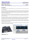
RL78G14 Motor Control Kit YRMCKITRL78G14
User Manual
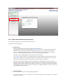
Introduction
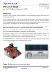
This document describes the Motor Control Kit (YRMCKITRL78G14) based on RL78/G14.
D011181 Rev.1.00
th
June 15 2012
D011181 Rev.1.00
th
June 15 2012
This platform drives a 3-phase Permanent Magnet Synchronous Motor (Brushless Motor) by using an advanced sensorless Field Oriented Control algorithm.
The phase currents measurement is done via three shunts which offer a very low cost solution avoiding any expensive
current sensor.
The main focus applications for this type of algorithm are compressors, air conditioning, fans, and so on.
The platform allows easy custom applications development, including an on-board small motor and a user-friendly PC
graphical user interface.
The platform can be powered directly by the PC USB interface or via an external power supply and in this case the USB
communication can be optically isolated.
An external power stage can be managed, in order to control higher power motors.
Target Device
RL78/G14 series
A-1
Contents
1.
Installation and Set-Up ...................................................................................................................... 4
1.1. Software Installation .......................................................................................................................... 4
1.1.1
Virtual UART USB Driver Installation on Windows XP ............................................................ 5
1.1.2
Virtual UART USB Driver Installation on Windows 7 ............................................................... 8
1.1.3
Confirmation of USB Driver Installation .................................................................................. 10
1.2. Stand Alone Demonstration Setup .................................................................................................. 11
1.2.1. Motor Connections ........................................................................................................................ 11
1.2.2. Set the Power Supply Selection .................................................................................................... 11
1.2.3.
Set the USB Interface Connection ............................................................................................. 11
1.2.4. Select the Internal Inverter ............................................................................................................ 12
1.3. Operating the Demonstration .......................................................................................................... 12
1.3.1.
Connecting the board ................................................................................................................. 12
1.3.2.
Stand Alone Demonstration Mode Operation ............................................................................ 13
1.3.3.
Demonstration Mode using the GUI .......................................................................................... 13
2.
Hardware Description ...................................................................................................................... 14
2.1. Power Supply Selection .................................................................................................................. 16
2.2. LED Description .............................................................................................................................. 17
2.3. Communications / Debug / Programming Interface Jumper Management ..................................... 18
2.4. Internal/External Power Stage Selection......................................................................................... 20
2.4.1.
Internal Power Stage Description .............................................................................................. 21
2.4.2.
External Power Stage Interface ................................................................................................. 22
2.4.2.1.
External Power Stage Interface Signal Definitions................................................................. 23
3.
Control MCU overview .................................................................................................................... 24
4.
RL78/G14 Motor Control Kit Specifications and Performance Data ............................................... 25
5.
PC User Interface (GUI) .................................................................................................................. 26
5.1. Launching the PC User Interface (GUI) .......................................................................................... 26
5.2. Function Button Description ............................................................................................................ 29
5.2.1.
Algorithm Selection .................................................................................................................... 29
5.2.2.
Parameter Setting ...................................................................................................................... 30
5.2.3.
System Monitor .......................................................................................................................... 30
5.2.4.
Main Control Window (Speed Control) ...................................................................................... 31
5.3. GUI Control Command Flow ........................................................................................................... 35
6.
Motor Calibration using the PC GUI Interface ................................................................................. 39
6.1. Stator Phase Resistance ................................................................................................................. 39
6.2. Start Up current ............................................................................................................................... 40
6.3. Maximum Current ............................................................................................................................ 40
6.4. Synchronous Inductance ................................................................................................................. 41
6.5. Tuning the initial Current Pi Gains .................................................................................................. 42
6.6. Tuning the Speed Pi Parameters .................................................................................................... 44
7.
Permanent magnets brushless motor model .................................................................................. 45
8.
Sensorless F.O.C. algorithm ........................................................................................................... 49
9.
Software Description ....................................................................................................................... 50
10. Start-up Procedure .......................................................................................................................... 53
11. Reference System Transformations in Detail .................................................................................... 55
12. PWM Modulation Technique ........................................................................................................... 56
13. Internal Representation of Physical Quantities ............................................................................... 57
14. List of variables used in “motorcontrol.c” ........................................................................................ 58
15. Application Customisation ............................................................................................................... 61
16. Renesas Flash Programmer Usage ................................................................................................ 62
17. IAR Embedded Workbench Usage ................................................................................................. 70
18. Online technical support and information .......................................................................................... 78
Revision History....................................................................................................................................... 79
General Precautions in the Handling of MPU/MCU Products ................................................................. 80
1.
Installation and Set-Up
The following section provides the information to install the software, projects and documentation for the
YRMCKITRL78G14 motor control kit and to be able to set up the hardware in order to run the built in
demonstration.
1.1. Software Installation
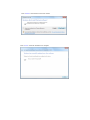
To install the software supplied with the kit, Place the CD-ROM into the PC drive
The installation should start automatically
If for any reason the CD fails to start automatically, please run the “setup.exe” file on the CD
Windows™ Vista and 7 users may see “User Account Control” dialog box. If applicable, enter the administrator
password and click <OK>. It is recommended that the user has sufficient administration rights to install the
software on the CD. The following shall be installed:
The following software shall be installed or copied onto the user’s PC
Motor Control GUI
IAR Embedded Workbench including documentation
Renesas Flash Programmer including documentation
RL78 IEC Self-Test Software (Source code) including documentation
YRMCKITRL78G14 IAR Embedded Workshop motor control project
Renesas Manual Navigator
Virtual UART USB Drivers
Please note that the IAR Embedded Workbench will require license registration. Please follow the instructions
during installation and ensure no other instance of the IAR Embedded Workbench is open.
The YRMCKITRL78G14 documentation shall be copied during installation and is designed to be viewed with the
Manual Navigator which is installed with this kit.
The following documentation shall be copied onto the user’s PC
RL78/G14 user manual
uPD0730 USB user manual
RJK0654DPB Power MosFet user manual
YRMCKITRL78G14 motor control kit user manual (This document)
YRMCKITRL78G14 design files and schematics
YRMCKITRL78G14 Quick start guide
15V BLDC Demonstration motor data sheet
E1 On chip debug/programmer user manual
Environmental documents (WHEE, RoHS)
Before any of the software can be used the Virtual UART USB drivers need to be installed
Two copies of the drivers are included in the installation process
YRMCKITRL78G14 kit installation
During the IAR Embedded Workbench Installation
Depending on the Windows operating system, the drivers should be used as follows
For 32bit Windows OS, 32bit USB drivers should be used (i.e. Windows XP, Vista and W7) and are
located here
C:\Program Files\Renesas\YRMCKITRL78G14\Virtual UART\32bit
if the YRMCKITRL78G14 installation is used
C:\Program Files\IAR Systems\Embedded Workbench 6.0\rl78\drivers\renesas\VirtualCOM\32bit
if the IAR installation is used
For 64bit Windows OS, 64bit USB drivers (i.e. Windows Vista and W7) and are located here
C:\Program Files\Renesas\YRMCKITRL78G14\Virtual UART\64bit
if the YRMCKITRL78G14 installation is used
C:\Program Files\IAR Systems\Embedded Workbench 6.0\rl78\drivers\renesas\VirtualCOM\64bit
if the IAR installation is used
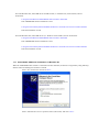
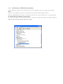
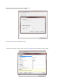
1.1.1 Virtual UART USB Driver Installation on Windows XP
When the YRMCKITRL78G14 board is connected to the host machine, the board is recognized by “Plug and Play”,
and the wizard for finding new hardware is started.
Select “No, not this time” and click “Next”
Select “Install from a list or a specific location (Advanced)” and click “Next”
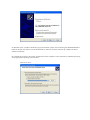
On Windows Vista, a window should also pop up with similar options when connecting the YRMCKITRL78G14
board for the first time. Select “Locate and install driver software” and then “Browse my computer for driver
software (advanced)”.
Set “Include this location in the search” and then browse the computer to select the directory indicated previously
for the appropriate operating system location.
Then click “Next”
If this window appears, click “Continue Anyway” to continue the installation.
Then click “Finish” to complete the installation wizard.
1.1.2
Virtual UART USB Driver Installation on Windows 7
When the YRMCKITRL78G14 board is connected to the host machine, the board is initially recognised as an
“Unknown Device” in the Device Manager. Right click on the “Unknown Device” and select “Update Driver
Software…” within the Device Manager window.
Select “Browse my computer for driver software”.
Please select the correct file location (32bit / 64bit) as indicated previously for the appropriate Operating system
Then click “Next”
Click “Install” when the driver has been found..
Click “Close” when the installation is complete
1.1.3 Confirmation of USB Driver Installation
After installing the USB driver, check that the driver has been installed correctly, according to the procedure
below.
Open the "Device Manager" (this will vary depending on the Windows Operating system used)
When the YRMCKITRL78G14 board is connected to the host PC, the “Ports (COM & LPT)” section should show
the "Renesas Electronics Starter Kit Virtual UART”.
The screen below shows that the COM port number is "COM23". Note that if the board is connected to a different
USB port connection, the COM port number will change.
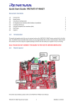
1.2. Stand Alone Demonstration Setup
The following information provides the initial setup for the YRMCKITRL78G14 motor control kit basic “out of
the” box” demonstration which can be used to check that the system is working correctly and provide a quick
demonstration for customers, exhibitions etc.
The following describes the default settings which configures the board for use with the USB supply and the
internal Inverter. Please ensure that no external power stage is connected to connector J10
1.2.1. Motor Connections
Connect the demonstration motor supplied in the kit, to the connector as shown below:
1.
2.
3.
4.
Red Motor wire to “U” connection
Black motor wire to the “V” connection
Green motor wire to the “W” connection
The Hall sensor wires should not be connected
Once connected, plug the motor connector into the board (J7)
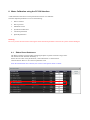
1.2.2. Set the Power Supply Selection
Check that jumpers JP1 and JP2 are both
connected between pin 4 and 6
Jumpers JP1 and JP2
1.2.3. Set the USB Interface Connection
Check that the following jumpers are connected as shown below.
JP3 pins 2 – 3
JP4 pins 2 - 3
JP5 pins 2 - 3
Jumpers JP3 to JP7
JP6 pins 2 - 3
JP7 pins 2 - 3
Note that this sets the USB interface to the “non isolated” mode
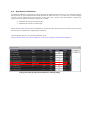
1.2.4. Select the Internal Inverter
The following jumpers should fitted to connect the power, control, current inputs and the PWM drive signals to
the internal inverter
JP10 fitted
JP11 fitted
JP12 fitted
JP13 fitted
JP14 fitted
Jumpers JP10 to JP19
JP15 fitted
JP16 fitted
JP17 fitted
JP18 fitted
JP19 fitted
Jumper JP8 and JP9 can be connected or open
Jumper JP8 and JP9
1.3.
Operating the Demonstration
Once the jumpers have been checked as described above and the motor is connected
Follow the sequence described below to run the demonstration
1.3.1.
Connecting the board
Connect the USB lead to the PC and then connect it to the YRMCKITRL78G14 board
The following LED should be lit (on):
DL7 USB supply from the PC and the step up regulator,
DL6 12V step-down converter output,
DL5 5V step-down converter output (logic supply).
The following LED’s are controlled by the RL78G14 MCU:
DL1 should blink at approximately ½ second interval (RL78G14 running),
DL2, DL3 should be off,
DL4 should be on (it is driven with an I/O output with period equal to sampling period interrupt).
1.3.2.
Stand Alone Demonstration Mode Operation
To start the demonstration sequence press the P4 button
The board should follow the following sequence:
The motor should start and accelerate to a steady speed
The motor will run at this speed and direction for approximately 10 seconds
The motor shall then reverse direction
Decelerate =>
Stop =>
Change direction =>
Accelerate to the previous speed =>
Continue operating for a further 10 seconds =>
The motor shall then stop
The sequence can be repeated by pressing the P4 button again.
The motor speed is defined by the Minimum and maximum speed settings.
When running from the hardware the demonstration speed is defined by the default settings in the motor
control IAR project or those set during a previous session when using the GUI
The basic speed is calculated as follows:Demonstration Speed = Min Speed + ((Max Speed – Min Speed) / 4)
This setting of the demonstration speed equation can be changed in the code contained in the “motorcontrol.c”
source file
1.3.3.
Demonstration Mode using the GUI
The YRMCKITRL78G14 demonstration can also be operated as described above using the control GUI.
To start the demonstration press the “DEMO” button in the PC GUI
The demonstration will follow the same sequence as described for the stand alone operation above.
If the GUI is installed and running, the graphs will be updated with the running data (Speed, Voltage and
Current) even if the demonstration is started from the push button on the board.
Note the “RPM SPEED” indicator does not operate in demonstration mode. The measured speed is
updated as normal. The demonstration speed should be the same if the minimum and maximum speed
settings have not been changed in the “parameter setting” window.
For further details please see the PC Control Interface section
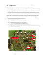
2.
Hardware Description
The YRMCKITRL78G14 starter kit is a single board motor control inverter, based on the new RL78/G14 series of
microcontrollers. The hardware includes a low-voltage 3-phase MOSFET power stage, the MCU control system, the
switching power supplies and the communications / debugging / programming interface.
To maximise the flexibility of the demonstration board, the following features are included:
A complete 3-phase inverter on-board with a low voltage motor, so it becomes easy to test the sensor-less
algorithm on the RL78G14.
Two RL78/G14 devices can be supported by the board
o
The default is the 100pin device (R5F104PJAFB)
o
64pin device (R5F104LEAFB)
o
The pin out of both RL78G14 devices are brought out to connectors JPUP1, 2, 3 and 4
USB Communications, Debugging and Programming interface via the uPD78F0730 USB MCU.
Connectors for hall sensors and encoder connections
Connection for an external power supply
On board power supply generation from either the USB or external supplies
A user “patch area” for external signal conditioning or use of other motor control algorithms
Sample BLDC Motor
External power stage interface.
The default device mounted on the board is the 100pin RL78/G14 device. If required this device can be removed and a
64pin RL78/G14 device fitted
The Communication/Debugging interface allows the user to control the inverter through the graphical user interface
(GUI), or to program the RL78/G14 with either the Renesas Flash Programmer or download and debug the motor
control program with the development IDE debugger. This interface uses the PC USB power supply.
When using external programming or debugging tools it is possible to fully isolate the communications interface to
avoid possibilities of electrical damage, especially when using the external power stage interface
The board can be fully powered either from the PC USB interface, or from an external power supply.
When the USB power is used, a step-up converter is used to obtain the inverter VBUS voltage necessary to generate the
voltages for the main board and the motor. In this mode the main system is not isolated from the PC and the current
available for the motor drive is limited to approximately 300mA.
When an external power supply is used the main board is fully isolated from the PC. The power for the motor is rated at
48Vdc @3A. It may be possible to supply more motor current, but it will be necessary to provide cooling for the
inverter stage power MosFets in order to keep the temperature of the power MosFets at around 600C
The internal power supplies (logic and for the driving system) are obtained through two step-down switching regulators,
in order to reduce heating and power consumption.
A patch area was added to allow the user to make hardware modifications/adjustments as necessary. This area can also
be used to support alternative motor drive algorithms, such as sensorless BLDC drive.
Please refer to the schematics for the details of the full hardware implementation.
PATCH AREA
INTERNAL POWER STAGE
STEP-DOWN
12V
HALL
SENSORS
INTERFACE
STEP-DOWN
5V
EXTERNAL
POWER
STAGE
INTERFACE
RL78G14 E1
interface
connector
STEP_UP
Internal/External
power stage
selection
POWER STAGE
INTERFACE
Communications
mode Jumper
selection
ENCODER
INTERFACE
User Switches
P4 is at the
bottom
RL78G14
MICROCONTROLLER
connections
ISOLATION
YRMCKITRL78G14 Board Overview
COMMUNICATION
2.1.
Power Supply Selection
There are two main ways to supply power to the board.
1.
The first is to use the PC USB supply, and in this case the current you can give to the motor is limited by
the USB interface. In this mode the USB interface is not isolated.
2.
The second is to use an external voltage DC source to supply the board.
The recommended operating voltage range is between 15Vdc and 48Vdc, max at 3Amps DC.
A power supply with more current could be used to increase the available for the motor. However it
recommended that the power MosFets are kept to a working temperature of approx. 600C so that some
form of air cooling will be needed.
In this setting the USB communications interface will be isolated from the inverter.
The selection between the two possibilities is made using jumpers JP1 and JP2, as shown below.
JP2-1
JP2-3
JP2-4
JP2-6
JP2-1
JP2-3
JP2-4
JP2-6
JP1-1
JP1-3
JP1-4
JP1-6
JP1-1
JP1-3
JP1-4
JP1-6
EXTERNAL SUPPLY SELECTION
USB SUPPLY SELECTION
Power supply Selection Jumpers (JP1 and JP2) configuration settings
Power supply Selection Jumpers (JP1 and JP2) location
Note: The figure shown above is with the jumpers in position 3 – 4
2.2.
LED Description
There are three LED’s on the board that show the status of the power supply of the board.
DL7 is connected to the USB supply from the PC, so it indicates that power is supplied to the USB port
and, therefore the complete communication section;
DL6 is connected to the 12V step-down converter output (VDRV12V) and indicates that the inverter drive
voltage is supplied.
DL5 is connected to the 5V step-down converter output (logic supply); it indicates that the control section
is supplied.
The other LED’s in the board (DL1, DL2, DL3 and DL4) are driven via software from the RL78/G14 MCU.
These have the following functions, but can be user programmable by editing the motor control project.
DL1 - This is set to indicate that the RL78/G14 is operating
DL2 - This is used to indicate a motor error
o Flashes quickly when there is an error, Off otherwise
DL3 - a Watchdog, Ram Parity, Illegal access reset is generated.
o Is set off when a normal power on or manual reset occurs
DL4 – Indicates the control loop interrupt timing. Lit to indicate operation
o The LED duty will change when idle or when the motor is running. This point or I/O pin can be
monitored with an oscilloscope
DL6
DL1, DL2, DL3, DL4
DL5
DL7
YRMCKITRL78G14 LED Locations
2.3.
Communications / Debug / Programming Interface Jumper Management
Using the communication interface, based on the uPD78F0730 USB MCU, it is possible to run the following
a.
Control GUI,
b.
Program the RL78G14 using the Renesas Flash Programmer (RFP) software
c.
Debug the RL78G14 using the IAR Embedded Workbench “TK” interface.
Please note that these functions cannot be operated at the same time as they all share the same USB interface
on the board. Also that it is advised that no other peripheral devices are connected to the USB port or hub
when using the motor control kit.
Selection of GUI or Programming/debugging is provided by jumpers (JP3, JP4, JP5, JP6 and JP7) as shown below.
The settings are also included on the board for reference.
GUI / OCD Jumper (JP3, 4, 5, 6 and JP7) locations
GUI or TK settings
Jumpers JP3 to JP7
JP3-1
JP3-2
JP3-3
JP3-1
JP3-2
JP3-3
JP4-1
JP4-2
JP4-3
JP4-1
JP4-2
JP4-3
JP5-1
JP5-2
JP5-3
JP5-1
JP5-2
JP5-3
JP6-1
JP6-2
JP6-3
JP6-1
JP6-2
JP6-3
JP7-1
JP7-2
JP7-3
JP7-1
JP7-2
JP7-3
PROGRAMMING / TK
OCD
VIRTUAL UART (GUI)
GUI / OCD Jumper (JP3, 4, 5, 6 and JP7) configuration settings
NOTE: It is also possible to debug the RL78G14 using the E1 emulator, through the dedicated connector J5.
Care should be made when operating from an external power supply, as this interface cannot be isolated
RL78/G14 E1
connector
E1 OCD Interface connector location
2.4.
Internal/External Power Stage Selection
The board offers the option of using either an internal MosFet power stage, or the complete interface to
connect an external power stage.
(Please note that the internal and external interfaces cannot be operated at the same time).
The power supplies, inverter drive signals and the other control and monitor signals are connected to the
external power stage connector J10. If an external power stage is connected, then the jumpers shown below
jumpers should be removed (NOT fitted).
When using the internal power stage the jumpers should be fitted and a connection to the external power stage
connector must not be connected.
The jumper selections are as described below:
First jumper group:
o
JP10
Internal U current analog channel selection
o
JP11
Internal V current analog channel selection
o
JP12
Internal W current analog channel selection
o
JP13
Internal bus voltage analog channel selection
Second jumper group:
o
JP14 (H), JP15 (L)
U phase driving signals
o
JP16 (H), JP17 (L)
V phase driving signals
o
JP18 (H), JP19 (L)
W phase driving signals
FIRST JUMPER GROUP:
JP13, JP12, JP11, JP10
SECOND JUMPER GROUP:
JP19, JP18, JP17, JP16, JP15, JP14
EXTERNAL POWER
STAGE CONNECTOR
J10
External Interface Connector and Jumper locations
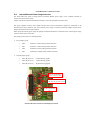
2.4.1. Internal Power Stage Description
The internal power stage is forms a complete 3-phase inverter bridge using discrete low voltage power
MosFets. (Renesas RJK0654DPB n-channel power MosFet)
The logic driving signals from the RL78/G14 MCU are connected to three IR MosFet drivers which take care
of the level shifting and charge pump generation for the MosFet gate drive.
The inverter phase currents are read through three shunts in the low sides of the bridge.
RJK0654DPB n-channel power MosFet 3-Phase Inverter
MosFet Gate Drive Interface (One Channel)
Please refer to the board schematic for the full details.
2.4.2. External Power Stage Interface
Since internal power stage allows only the management of low voltage / low current motors, an interface with
an external power stage is provided. This allows the RL78/G14 MCU together with the control GUI or IDE
debugger to control a high voltage high power motor via a suitable external inverter unit.
Please find below the signal connection interface for the external power stage interface connector J10.
Temperature analog signal
1
2
Ground
Bus voltage analog signal
3
4
Ground
U current analog signal
5
6
Ground
V current analog signal
7
8
Ground
W current analog signal
9
10
Ground
Fault digital signal
11
12
U phase low switch command
Ground
13
14
V phase low switch command
Ground
15
16
W phase low switch command
Ground
17
18
U phase high switch command
Ground
19
20
V phase high switch command
Ground
21
22
W phase high switch command
Ground
23
24
SUP-1
SUP-1
25
26
SUP-2
Hall A digital signal
27
28
Hall B digital signal
Hall C digital signal
29
30
SUP-2
Encoder A digital signal
31
32
Encoder B digital signal
Encoder Z digital signal
33
34
Ground
External Interface Connector - Signal Connections
2.4.2.1.
External Power Stage Interface Signal Definitions
The following provides a short explanation of the external power stage interface connections
Please refer to the circuit schematics for full details.
Analogue Signals
The analog signals are inputs and should always be in the range 0V to 5V. It may be necessary to adjust when
a different motor is used and the value of the shunt resistor is changed
Drive Signals
The driving signals are outputs and are at logic (5V) level, and can be set as active high or active low
(This can be defined in the motor control project)
Alarm Signal
The alarm is an input and it is active low (no alarm level = 5V).
A pull-up is included on the board in case there is no connection to J10
Hall and Encoder Signals
The hall and the encoder signals are logic inputs and all have appropriate pull-up resistors
Supplementary Signals
Signal “SUP1”, connector pins 24 and 25 can be connected to:
1.
The internal power stage bus voltage (VBUS) by connecting Jumper 9 pins 1 - 2
2.
The internal power stage 12V drive voltage (VDRV12V) by connecting Jumper 9 pins 2 - 3
3.
Unconnected. Jumper 9 left open.
Signal “SUP-2” connector J10 pins 26 and 30 can be connected to
1.
2.
The logic supply +5V by connecting jumper JP8
Left unconnected
NOTE:
Care should be taken with the connections of Jumpers 8 and 9, when using the external interface
as these supply the local board 5V and either the VBUS or VDRV voltages to the external power stage.
It is recommended that the jumpers are removed to avoid shorting the power supplies together when an
external power unit is used, unless it is necessary to either supply or these voltages to the
3.
Control MCU overview
The RL78/G14 is a family of MCU’s featuring the high-performance RL CPU core.
Single cycle instruction execution, with enhanced hardware support for multiply, divide and MAC operations
Below is a summary of the RL78G14 features:
RL78G14 CPU
High-speed: 32MHz clock
High performance: 41MIPS @32MHz
Low current consumption: only 4.6mA @ 32MHz
MUL, DIV, MAC hardware instructions
Barrel shifter
MEMORY AND PACKAGES
16KB Flash/2.5KB RAM to 256KB Flash/24KB RAM
Up to 8KB Data Flash
30pin to 100pin package options
FEATURES
1% 64MHz internal oscillator
64MHz 16bit Timers
o
o
o
3-phase 16bit PWM timer with dead time (Timer RD)
Multifunction timer with encoder interface (Timer RJ)
Timer Array Unit (TAU) and multifunction Timer (RG)
10-bit A/D converter up to 12 channels, 2channel 8bit DAC
Window Comparator
Event Link and Data Transfer controllers (ELC & DTC)
Real Time Clock
Independent Windowed Watchdog
Self-Test functions (RAM/SFR Protect, ADC, System Clock Monitor, RAM Parity, Port Verify)
Large-capacity flash memory units capable of high-speed operation are included as on-chip memory, significantly
reducing the cost of configuring systems.
The main application fields of this MCU include: Small household Appliances, Fans, Pumps and Power Tools.
RL78/G14 Typical Block Diagram
4.
RL78/G14 Motor Control Kit Specifications and Performance Data
The specifications for the on board inverter and for the sensor-less algorithm implemented are as follows:
External Supply voltage range: 15V to 48Vdc.
Supply current: 3A max. (No Forced cooling)
Maximum continuous output power 100W.
Current reading technique: three shunt.
Motor Control Timer Clock frequency up to 64MHz
o PWM switching frequency: up to 24KHz.
Sampling rate: max 8KHz.
o Used CPU bandwidth: <70% @ 8KHz sampling rate.
RL78G14 – R5F104PJAFB
o 256KB Flash, 24KB RAM, 8KB Data Flash
RL78G14 – R5F104LEAFB
o 64KB Flash, 5.5KB RAM, 4KB Data Flash
YRMCKITRL78G14 kit utilisation
o Flash occupation: 15KB
o Ram occupation: 2kB
5. PC User Interface (GUI)
The User Interface is installed automatically during the CD-ROM installation.
The PC Interface uses the USB connection to communicate with the RL78G14 board so before use please make sure
that the Virtual UART drivers are installed as described in section 1.1.1
5.1. Launching the PC User Interface (GUI)
Note that for Windows Vista and Windows 7 it is necessary to run the GUI as “Run as administrator”
It is possible to set the operation to permanently enable the “Run as administrator” option in the windows start
menu. To enable this option perform the following sequence
a.
b.
c.
d.
e.
Right click on the “motor Control Demo” icon
Select Properties
Select Advanced
Click the “Run as administrator” button
Press “OK” twice to return
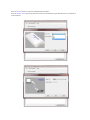
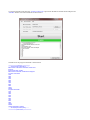
To open the PC GUI click on the “Motor Control Demo” ICON in the start menu.
The GUI should open as shown below
To connect the GUI to the YRMCKITRL78G14 board follow the sequence
If more than one configuration file is located in the GUI installation directory, then the user has to
select the appropriate configuration (setup) file. Otherwise the default configuration file (setup.ini)
is selected automatically and this part can be skipped.
Note the setup and configuration can be customised by editing the setup.ini file and then saving as
the same or alternative file name.
If the setup file is not automatically selected, then first select the “Select board setup” drop down
bar in the top left hand corner of the GUI panel. Then select the G14 configuration file (i.e. setup)
as shown below and close the box
Select the setup
configuration file
Next select the “Com Port selection” drop down box and select the communications port that
the YRMCKITRL78G14 board is connected to, close the drop down box and click the
“connect” button as shown below
Select the com port.
The press the connect button
The GUI should now be connected to the board as shown below
GUI connected to the
board
5.2. Function Button Description
5.2.1. Algorithm Selection
At this time the only algorithm available is the sensorless F.O.C algorithm Pressing the
“Verify Jumper Settings” button opens the default settings for the board
Pressing the “Verify Jumper Settings” button opens the default settings for the board.
This allow the default configuration to be set without reference to the user manual or quick start guide
5.2.2. Parameter Setting
This window allows the run time parameters to be set and changed. When the parameter set is changed and re
written the saves these in the non-volatile memory (Data Flash or EERPOM)
Before running the motor, check that the Parameters Settings displayed like the speed range and the number of
polar couples etc. are in-line with the motor to be used or tuned (See section 12).
The parameters can be reloaded into the GUI by pressing the “Reload” button to read all the parameters that are
stored in the non-volatile memory (eeprom or data flash).
In case of setting incorrect or inconsistent parameters, the original default parameters can be restored from the
MCU flash memory (Not Data Flash or EEPROM) by following the operation shown below
1. Enter the magic number “33” in the first line called: “00. Default Parameters setting”
2. Click the “Write” button in the parameter setting window
3. Then hardware RESET the RL78 by pressing the P6 button on the board.
4. Click the “Reload” button to get the default parameters defined in the “customize.h” header file in
the IDE workspace.
5.2.3. System Monitor
This window shows the status of the RL78MCU self-test results and also shows if there is a motor error
The motor error/alarm is also shown in the main “Speed Control” Window
5.2.4. Main Control Window (Speed Control)
This window provides the main control window for the board
It includes the following features
a.
RPM Control
Allows manual control of the motor including speed and direction.
The speed reference can be varied using the “RPM CONTROL” pointer, which can be either moved
with the mouse, or with the value written, directly into the text box. A value written as a positive
value (i.e. 3000) will operate the motor in a clockwise direction, with a value written as a negative
value (i.e. -3000) will operate the motor in the reverse (Anti-clockwise) direction
“PAUSE”, “GO” and “REVERSE” control buttons are also included.
The “DEMO” button enters the pre-set demonstration command sequence, which operates the motor
with the same sequence as described previously for the “Stand Alone” demonstration. (i.e. the same
operation as pressing the button P4 on the board). No other settings are required
The two bars shown in the RPM Control wheel indicate the “minimum speed” point as set in the
parameter settings. Below the minimum speed the motor does not operate and above the minimum
speed the motor operates normally at the reference speed set. The setting of the minimum speed can
be displayed by the tool tip as the mouse is moved over the minimum indicator. This is the value set
in the parameter settings window.
b.
Property Monitor
This windows shows the main motor operating parameters
The monitor graph can be set to display any of monitored properties, by clicking on the required
property to be viewed
The run time data can be saved to an Excel file by clicking on the “Save data to file” button
This will open a dialogue box to select the filename and location of the file that the data is saved into.
A control bar will appear to allow the use to Start, Pause or Stop the data recording process
c.
Speed Control Graphs
There are three graphs that monitor the operation of the motor. SPEED, VOLTAGE and CURENT
The speed graph shows the Target and Measured Speed
The Voltage graph shows the VBUS Supply value, Direct, Quadrature and Total Voltages
The Current graph shows the Total, Direct and Total currents
Any individual graph can be expanded by pressing the “ZOOM” button. When a graph is
“ZOOMED” then only this graph is visible in the GUI display. Data for all graphs continues to be
updated in the background.
The previous data timeline of the graphs can be seen by using the slide control next to the
“STOP UPDATE” button
The graphs update can be stopped by clicking on the STOP UPDATE
Once the GUI is connected, open the main control window by pressing the “Speed Control” button. Through this
window, the user can control the speed reference to the board, and can view all the reference values and measurements.
in the three “oscilloscope” graphs.
The motor can be controlled by the “RPM CONTROL” section by either moving the point to the desired speed and
direction or setting the speed in the text box. The “DEMO” button performs the same operation as described previously.
Once the motor is in operation the graphs will start to update together with the measured values in the
“PROERTY MONITOR” window as shown below
d.
Alarm Codes
There are three “alarm codes used in the GUI and embedded software
1.
2.
3.
EEPROM error alarm
Inverter error
Loss of phase error
The alarm codes usually can be cleared by resetting the motor speed back to zero. In some
circumstances it is necessary to perform a manual reset of the RL78/G14 to clear the error. This may
reset the connection between the board and the GUI.
e.
Saving Monitor Property Data to a file
It is possible to save the measured data displayed in the “PROPERTY MONITOR” window to a
“comma separated values` (csv) excel file for offline analysis and review
This is started by clicking the “Save Data to file” button located at the bottom of the “PROPERTY
MONITOR” window.
This will open a media player style control bar which allows the user to
1.
Stop recording , close the media bar and close the file
2.
Pause / Resume recording
3.
Reset Recording (Note this will overwrite the data in the file)
Each update of the GUI, monitor data is saved and will create a new entry in the excel file.
When the button is first pressed the user will be prompted for the file name of the file to be used.
Please note that recording start as soon as the file is opened even if the motor is not yet running.
This can be a new file or and existing file created previously. Note that a new session will overwrite
any previous data in the file
Due to the nature of a “csv” file is may be possible on some versions of MS Office that the data is not
correctly separated into columns. This can be corrected by changing the settings in the MS Office
Excel program when the “csv” file is first opened so that it is saved correctly in future usage.
Please refer to the Microsoft Office installation for further information.
5.3. GUI Control Command Flow
The following information shows the command and control flow for the communications between the PC GUI and
the RL78/G14 motor control board firmware.
ASCII codes used as commands: “!” = 0x21, “#” = 0x23, “?” = 0x3F, “W” = 0x57, “c” = 0x63, “w” = 0x77
If the address "a" specified in the Master command is <NUM_PAR_EQP (number of eeprom parameters),
then the parameter is read or written depending on the command.
Otherwise if the address “a” >=NUM_PAR_EQP, then a parameter in the ram table (userif.h) is read or written;
Its address (location) in the ram table is defined by “a” - NUM_PAR_EQP.
5.3.1.
Master Control Codes
Frame Format
l i
s o a n D1 .. Dm k
where
l = frame total length (1 byte)
i = master string identifier ('?')
s = station address (1 byte)
o = operation code (1 byte)
a = data address (1 byte)
n = data number (1 byte)
Dx = x-th data byte (1 byte)
k = checksum (1 byte)
Master Command codes:
'c' = check
'w' = word reading (1 word = 2 bytes)
'W' = word writing (1 word = 2 bytes)
Possible master frames (Commands):
Check: l ? s c k
(l=5)
Word read: l ? s w a n k
(l=7)
Word write: l ? s W a n D11 D10 .. Dn1 Dn0 k
5.3.2.
Slave Control Codes
Slave string:
l i s o a n D1 .. Dm k
where
l = frame total length (1 byte)
i = slave string identifier ('!' = OK answer, '#' = NOK answer)
s = station address (1 byte)
o = operation code (1 byte)
(l=7+2*n)
a = data address (1 byte)
n = data number (1 byte)
Dx = x-th data byte (1 byte)
k = checksum (1 byte)
Slave Command Code Operation:
'c' = check answer
'w' = word reading answer (word = 2 byte)
'W' = word writing answer (word = 2 byte)
Possible slave frames (Responses):
Nok: l # s o k
(l=5)
Check: l ! s c k
(l=5)
Word read: l ! s w a n D11 D10 .. Dn1 Dn0 k
Word write: l ! s W k
5.3.3.
(l=7+2*n)
(l=5)
Communications Examples
Example 1
PC request of reading 16 words from the structure UIF_R, starting from the second position
(UIF_R.ram_tab[1], .., UIF_R.ram_tab[16]):
Byte
Code
Meaning
0
07
Number of bytes in the frame
1
3F
Master command string indicator ("?")
2
00
Station address (it is always 0 in our boards)
3
77
word reading operation "w"
4
41
data start address
(1(address in UIF_R.ram_tab) + 40h (offset to add for ram reading/writing))
5
10
number of data words (0x10, 16dec)
6
39
checksum
Board answer:
Byte
Code
Meaning
0
27
Number of bytes in the frame (27h=39dec)
1
21
Slave string indicator "!"
2
00
Station address (it is always 0 in our boards)
3
77
word reading operation "w"
4
41
data start address (1(address in UIF_R.ram_tab)+40h(offset to add for ram reading))
5
10
number of data (10h=16dec)
6
00
MSB of the 1st word of data (UIF_R.ram_tab[1]=UIF_R.var.rpm, speed)
7
00
LSB of the 1st word of data
8
00
MSB of the 2nd word of data (UIF_R.ram_tab[2]=UIF_R.var.fre, imposed frequency)
9
00
LSB of the 2nd word of data
10
00
MSB of the 3rd word of data (UIF_R.ram_tab[3]=UIF_R.var.id, d axis current)
11
00
LSB of the 3rd word of data
12
00
MSB of the 4th word of data (UIF_R.ram_tab[4]=UIF_R.var.iq, q axis current)
13
00
LSB of the 4th word of data
14
00
MSB of the 5th word of data (UIF_R.ram_tab[5])
15
00
LSB of the 5th word of data
16
00
MSB of the 6th word of data (UIF_R.ram_tab[6])
17
00
LSB of the 6th word of data
18
00
MSB of the 7th word of data (UIF_R.ram_tab[7]=UIF_R.var.vb, bus voltage)
19
18
LSB of the 7th word of data
20
00
MSB of the 8th word of data (UIF_R.ram_tab[8])
21
00
LSB of the 8th word of data
22
00
MSB of the 9th word of data (UIF_R.ram_tab[9]=UIF_R.var.all, alarm)
23
01
LSB of the 9th word of data
24
00
MSB of the 10th word of data (UIF_R.ram_tab[10])
25
00
LSB of the 10th word of data
26
00
MSB of the 11th word of data (UIF_R.ram_tab[11])
27
00
LSB of the 11th word of data
28
00
MSB of the 12th word of data (UIF_R.ram_tab[12])
29
00
LSB of the 12th word of data
30
00
MSB of the 13th word of data (UIF_R.ram_tab[13])
31
00
LSB of the 13th word of data
32
00
MSB of the 14th word of data (UIF_R.ram_tab[14])
33
00
LSB of the 14th word of data
34
00
MSB of the 15th word of data (UIF_R.ram_tab[15])
35
00
LSB of the 15th word of data
36
00
MSB of the 16th word of data (UIF_R.ram_tab[16])
37
00
LSB of the 16th word of data
38
69
checksum
Example 2
PC request of writing 4 words in the structure UIF_W, starting from the third position
(UIF_W.ram_tab[2], .., UIF_W.ram_tab[5]):
Byte
Code
Meaning
0
0F
Number of bytes in the frame (0Fh=15dec)
1
3F
Master string indicator. ("?")
2
00
Station address (it is always 0 in our boards)
3
57
word writing operation "W"
4
42
data start address (2(address in UIF_W.ram_tab)+40h(offset to add for ram reading/writing))
5
04
number of data
6
03
MSB of the first word of data (value (03E8h=1000dec) to be written in
UIF_W.ram_tab[2] = UIF_W.var.rif (speed reference)
7
E8
LSB of the first word of data
8
00
MSB of the second word of data (value to be written in UIF_W.ram_tab[3], not used)
9
00
LSB of the second word of data
10
00
MSB of the third word of data (value to be written in UIF_W.ram_tab[4], not used)
11
00
LSB of the third word of data
12
00
MSB of the fourth word of data (value to be written in UIF_W.ram_tab[5], not used)
13
00
LSB of the fourth word of data
14
E7
checksum
Board answer (indicates that the request is received and processed):
Byte
Code
Meaning
0
05
Number of bytes in the frame
1
21
Slave string indicator "!"
2
00
Station address (it is always 0 in our boards)
3
57
word writing operation "W"
4
E6
checksum
6. Motor Calibration using the PC GUI Interface
A full calibration of the motor can be performed via the PC User Interface.
The most important parameters to test are the following:
1.
Stator resistance
2.
Start-up current
3.
Maximum current
4.
Synchronous inductance
5.
Current PI parameters
6.
Speed PI parameters
Warning:
Do not try to start the motor before entering the initial calibration parameters otherwise the system could be damaged.
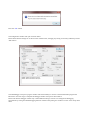
6.1. Stator Phase Resistance
The Phase resistance can be found by measuring the phase-to-phase resistance using a meter.
The measured value should be divided by 2.
Please enter the value in the parameter 08, “Stator Resistance” as shown below.
Click the button “Write” to save the new parameter value.
Since the measurement unit is Ohm/10, the value 23 of the picture means 2.3 Ohm.
6.2. Start Up current
The start-up current parameter is responsible for the proper motor start-up. Please enter an average value that will
not damage the motor. This value can be increased slowly if the motor fails to start at the end of the procedure.
Click the button “Write” to save the new parameter value.
Note: The value 3 in the picture below means 0.3 Amperes.
Setting the start-up current during motor tuning
6.3. Maximum Current
Maximum current specifies the maximum current to be imposed.
It should be set accordingly the inverter and the motor specifications, and as required by the application.
Click the button “Write” to save the new parameter value.
The value 3 in the picture below means 0.3 Amperes.
Setting the maximum current for motor tuning
6.4. Synchronous Inductance
Synchronous Inductance represents the average synchronous inductance of the motor (it is an equivalent quantity
that represents the auto and mutual interactions between the phase currents); it is usually low in surface magnets
motors; it can be neglected for the first tuning of the motor, but a wrong value will introduce a phase error
proportional to the load, so the tuning strategies can be either:
Maximize the torque at a rated current;
Minimize the current at a rated torque.
Please enter the value zero for the first calibration as shown below (the first start-up has to be done with no-load; in
this case there is no phase error neglecting the inductance).
Click the button “Write” to save the new parameter value.
Since the measurement unit is Henry/10000, the value 100, for example, means 10mH (milliHenry)
Setting the initial Synchronous Inductance during tuning
6.5. Tuning the initial Current Pi Gains
Current PI parameters allow a proper current control of the motor and the system.
The software offers a particular procedure to help the tuning of the current PI gains. An oscilloscope is needed to
see the response of the system to the stimulation; the figure below is showing the Test Point TP1 to be used for the
calibration.
TEST
POINTS
GROUND
REFERENCE
Current Pi Gain Setting – Monitor point Signal Connections
First of all it is necessary to enable the “current PI tuning mode”, and this can be done entering the magic value “22” in
the first parameter (“Default parameters setting”) in the “setup” and click on the button “Write”.
Now perform a hardware reset on the RL78G14, so the calibration procedure of the Current PI coefficient is enabled.
In the parameters list, please set the current PI coefficients: Kp and Ki to “1” as shown below:
Initial Setting of the Current Kp and Ki gains for motor tuning
Connect the oscilloscope probes to the Test Point (TP1) and to the Ground of the board.
The next step is to generate a current step and capture the current PI controller response in order to tune the current PI
coefficients. To generate the current step and check the response on the oscilloscope, please enter “1” in the parameter
17, “PI Tuning trigger” and click on the button “Write”. This will generate a current step reference which amplitude is
equal to the value specified as start-up current. In the oscilloscope you will observe the internal measurement of the
obtained current, normalized in such a way that when the signal is equal to 4V the current is equal to the requested one.
So the tuning procedure consists in varying the PI gains in order to make the signal equal to 4V in the fastest possible
way, without oscillation.
Please find below in the picture some examples of the different responses you may obtain.
Test Point 1 (TP1) Oscilloscope Tuning Outputs
Keep in mind that the proportional gain is the responsible of the “reactivity” of the system, while the integral gain
allows reducing to zero the steady state error. An excess of proportional gain will produce high frequency
oscillations (usually with audible noise), while an excess of integral action will produce lower frequency
oscillations. Note also that if the gains are too low, no answer is produced; increasing the parameters, at a certain
level, the current obtained will be enough to move the rotor, which will “align”; from this point in advance, don’t
move the rotor by hand, and you will see valid answers in the oscilloscope. The final rise time will depend on the
motor you are using, but usually a rise time lesser than 1ms can be obtained.
After tuning the current PI parameters manually reset the board in order to return to the “normal” operation mode.
6.6. Tuning the Speed Pi Parameters
Speed PI proportional gain (par. 13, “Speed Loop Kp”) and integral gain (par. 14, “Speed Loop Ki”) should be
tuned in the real application and under load conditions.
As starting values, low values can be chosen; they can be increased at medium working speed until instability
arises; (high frequency instability is related to the proportional value too high, low frequency instability is related to
integral value too high). When instability arises, the value should be halved. Some kind of tuning of speed
parameters can be performed using high values of acceleration ramp, and imposing speed reference variations, as
done with the current PIs.
The PI calibration procedure should be iterated till the desired system response is reached. The speed reference
could be changed depending on the motor/application. You can find below two graphs indicating an example of
tuning procedure; this procedure should be made using the real working environment.
Speed parameters can influence the success of the start-up phase: if the algorithm fails in this phase, giving alarm
n°3, try modifying the speed proportional gain first, and then the integral gain.
Speed Pi Integral calibration Flow Chart
Speed Pi Proportional calibration Flow Chart
7. Permanent magnets brushless motor model
The synchronous permanent magnets motor (sinusoidal brushless motor) is widely used in the industry. More and more
home appliance makers are now using such brushless motor, mainly because of the intrinsic motor efficiency.
The permanent magnet motor is made with few components:
A stator formed by stacking sheared metal plates where internally the copper wiring is wound, constructing the
stator winding.
A rotor in which permanent magnets are fixed.
Two covers with ball bearings that keep together the stator and the rotor; the rotor is free to rotate inside the
stator.
“a” winding
“b” winding
ia
Motor axis
(shaft)
+
va
“a” winding
magnetic axis
vb
ic
ib
+
vc
+
How current flows into
“a” winding
“c” winding
PMAC Motor Model
The working principle is quite simple: if we supply the motor with a three-phase system of sinusoidal voltages, at
constant frequency, in the stator windings flow sinusoidal currents, which create a rotating magnetic field.
The permanent magnets in the rotor tend to stay aligned with the rotating field, so the rotor rotates at synchronous speed.
The main challenge in driving this type of motor is to know the rotor position in real-time, so mainly implementation
are using a position sensor or a speed sensor.
In our implementation, the system is using either one or three shunts to detect the rotor position in real-time.
Let’s analyse the motor from a mathematic point of view.
If we apply three voltages va(t), vb(t), vc(t) to the stator windings, the relations between phase voltages and currents
are:
d a
dt
d
v b R S ib b
dt
d
v c RS ic c
dt
v a RS ia
- i is the magnetic flux linkage with the i-th stator winding.
- RS is the stator phase resistance (the resistance of one of the stator windings).
The magnetic flux linkages i are composed by two items, one due to the stator currents, one to the permanent magnets.
axis
c axis
a
b’
c’
m
’
a axis
c
’
axis
b
’
a’
b axis
Real axes (a, b, c) and equivalent ones (, ); a fixed amplitude vector can be completely determined by its
position respect the (, ) system (angle )
The permanent magnet creates a magnetic field that is constant in amplitude and fixed in position in respect to the rotor.
This magnetic field can be represented by vector m whose position in respect to the stator is determined by the angle
between the vector direction and the stator reference frame.
The contribution of the permanent magnets in the flux linkages depends on the relative position of the rotor and the
stator represented by the mechanical-electric angle.
It is, in every axis, the projection of the constant flux vector m in the direction of the axis:
a Lia m cos( )
b Lib m cos( 2 3 )
c Lic m cos( 4 3 )
Supposing that the rotor is rotating at constant speed (that is: (t) = t) the flux linkages derivatives can be calculated,
and we obtain:
dia
m sin( )
dt
di
vb RS ib L b m sin( 2 )
3
dt
di
vc RS ib L b m sin( 4 )
3
dt
v a RS i a L
A “three phase system”, may be represented by an equivalent “two phase system”. So there by using specific
transformations, our three equations system is equivalent to a two equations system. It is basically a mathematical
representation in a new reference coordinates system.
In the two phases (,) fixed system the above equations become:
v RS i
v RS i
d
dt
d
dt
For the magnetic field equations, we got:
Li m Li m cos( )
Li m Li m sin( )
After performing the derivation:
d
di
di
L m sin( ) L m
dt
dt
dt
d
di
di
L
m cos( ) L
m
dt
dt
dt
Finally, we obtain for the voltages in (,) system:
di
m
dt
di
v RS i L
m
dt
v RS i L
A second reference frame is used to represent the equations as the frame is turning at the rotor speed. So the “d” axis is
chosen in the direction of the magnetic vector m, and with the “q” axis orthogonal to the “d” axis. The new reference
system is (d, q).
The reference frame transformations from the (,) system to the (d, q) system depends on the instantaneous position
angle .
So we obtain two inter-dependant equations in the (d, q) system:
did
Liq
dt
diq
vq RS iq L
Lid m
dt
vd RS id L
These two equations represent the mathematical motor model.
Vd
1/(R+sL)
+
Id
+
L e
pL
load
Vq
+
1/(R+sL)
Iq
(3/2)p
+
1/(B+sJ)
mec
e
p
Vd and Vq Equation Diagram
A control algorithm which wants to produce determined currents in the (d, q) system must impose voltages given from
the formulas above. This is ensured by closed loop PI control on both axis “d” and “q” (Proportional Integral).
Since there is a mutual influence between the two axes, decoupling terms can be used.
In the block scheme the mechanic part is included, where “p” is the number of pole pairs, while “B” represents friction,
“J” the inertia, “load“ the load torque and “” the motor torque:
3
2
p
The angular speed is represented in the scheme as e to distinguish the electrical speed from the mechanical one.
Let’s now consider the equations we have seen in (,) system:
v RS i
v RS i
d
dt
d
dt
These equations show that magnetic flux can be obtained from applied voltages and measured currents simply by
integration:
t
0 (v RS i )dt
0
t
0 (v RS i )d
0
Furthermore:
m cos( ) Li
m sin( ) Li
If the synchronous inductance L is small, the current terms can be neglected, if not they have to be considered. In
general:
t
x m cos( ) Li 0 (v RS i )dt Li
0
t
y m sin( ) Li 0 (v RS i )dt Li
0
So in the (,) system phase we obtain from the flux components:
arctan( x y)
The system speed can be obtained as the derivative of the angle.
d
(t )
dt
Based on this, a sensor-less control algorithm was developed to give the imposed phase voltages, to measure phase
currents, to estimate the angular position and finally the system speed.
8. Sensorless F.O.C. algorithm
Please, find below the sensor-less FOC algorithm block diagram.
0 [Idref]
Id PI
+
Vd
Vq
(d, q) →
(, )
(, ) →
(u, v, w)
V
V
PWM
Modulation
Motor
ref
Speed PI Iqref
+
+
Current
Reading (z-1)
Iq PI
z-1
z-1
z-1
z-1
-
-
z-1
est
Speed
estimation
Idmea
Iqmea
est
(, ) →
(d, q)
Flux Phase
estimation
Imea
I mea
(u, v, w) →
(, )
Sensorless F.O.C algorithm
Iumea
Ivmea
9. Software Description
In the YRMCKITRL78G14 kit the software is working on an RL78G14 [32MHz].
The total software uses the following resources:
1) FLASH
15Kbytes
2) RAM :
2Kbytes
Please Note that this data also include the communication interface and the demo board management.
The following flow charts show the software implementation of the motor control part of the software
Software organization
Hardware and software initialization
Interrupt enabling
125s Interrupt
10ms Main loop
Software Structure
Main Program
Eeprom parameters upload
A/D channels offset reading
Peripherals initialization
Variables initialization
Interrupt enabling
Main loop
synchronization
cnt_int == 0 ?
NO
YES
cnt_int = NUM_INT
Main loop body
Speed ramp management
Communication management
General board management
Parameters modification management
Main Control Flow
Control Interrupt
Phase currents (iumea, ivmea) reading
Transformations (using the phase angle ):
(iumea, ivmea) → (iamea, ibmea) → (idmea, iqmea)
Read DC Link voltage vbus
Phase angle update: = new
Current PI controls use (idref, iqref), (idmea,iqmea) to produce (vdout, vqout)
Transformations (using the phase angle ):
(vdout, vqout) → (vaout, vbout) → (vuout, vvout)
PWM output commands generation (using vuout, vvout)
vbus is used to calculate maximum phase voltage (used in current PI controls)
Phase estimation based on old_vaout, old_vbout, iamea, ibmea,
produces new estimated phase angle est
Voltage memories update: old_vaout = vaout, old_vbout = vbout
Speed estimation produces est
Estimation errors detection (if errors an alarm is produced)
YES
NO
Start-up in progress?
Start-up procedure produces idref, iqref, stup
idref = 0
new = stup
Speed PI control uses (ref, est) to obtain iqref
new = est
Main loop
synchronization
cnt_int > 0 ?
NO
YES
--cnt_int
Motor Control Interrupt Processing
10. Start-up Procedure
When the motor is in stand-still, the phase of the permanent magnet flux vector cannot be detected with the used
algorithm. So an appropriate start-up procedure has to be applied.
The idea is to move the motor in feed-forward (with higher current than that required to win the load), till a speed at
which the estimation algorithm can work. Then the system can be aligned to the estimated phase, and the current can be
reduced to the strictly necessary quantity.
The following graph illustrates the strategy used (the suffix “ref” stands for reference, the suffix “mea” stands for
measured).
idref
idmea
iqref
iqmea
speedref
sstart
istart
id0
iq0
t0
t1
t2
t3
t
Start Up Process Graph
Referring to the graph, the start-up procedure (in case of three shunts current reading) is described below.
At the beginning t0, the system phase is unknown. No current is imposed to the motor; the system phase is arbitrarily
decided to be a = 0. All the references: idref, iqref and speedref are set to zero.
From the moment t0, while the iqref and the speedref are maintained to zero, idref is increased with a ramp till the value
istart is reached at the moment t1.
The references are referred to an arbitrary (da, qa) system based on the arbitrary phase a. From this moment, the phase
estimation algorithm begins to be performed, and the estimated phase is est.
The components of the current referred to the arbitrary (d a, qa) system are controlled to follow the references by the
current PI controllers, so they will be id=istart and iq=0. If we refer the measurements to the estimated phase we would
obtain those which in the graph are called id mea and iqmea (referred to (d, q) estimated system); since the phase est is still
not correctly estimated, idmea and iqmea have no physical meaning.
At t = t1, while iqref is maintained to zero and idref is maintained to its value istart, speedref is increased with a ramp till the
value sstart is reached at t = t2. The system phase a(t) is obtained simply by integration of speed ref; in the meanwhile, the
phase estimation algorithm begins to align with the real system phase. Furthermore id mea and iqmea begin to be similar to
the real flux and torque components of the current.
The interval (t2-t1) is the start-up time, and it is supposed to be large enough to allow the estimation algorithm to reach
the complete alignment with the real phase of the system.
At t = t2, the phase estimation process is supposed to be aligned. At this point a reference system change is performed:
from the arbitrary (da, qa) reference to the (d, q) reference based on the estimated phase est.
The system reference change is performed as follows:
The current references in the (da, qa) system, idref=istart and iqref=0, are projected in the fixed system (, ), to
compute the instantaneous current components; the same is done with the integral parts of the current PI
controllers, which are the mean voltages required to obtain those currents; in this way we obtain i, i, v, v.
The phase is updated to est.
The and components obtained before are projected into the new reference system (d, q), giving the new
current reference values id0, iq0 and the new PI integral memories vd0, vq0; the speed PI integral memory is
loaded with the q current reference.
After t > t2 , the normal control is performed, based on the estimated phase est; the speed reference is increased with the
classical ramp; the id current reference is decreased with a ramp, till it reaches the value zero at the moment t 3; then it is
maintained to zero; the iq current reference is obtained as output of the speed PI controller.
11. Reference System Transformations in Detail
Find below the detailed equations used for the coordinates transformations.
2
1
1
(gu gv g w ) ga
3
2
2
2 3
3
1
1
g (
gv
gw )
(gv g w )
(gu 2gv )
3 2
2
3
3
g
(u, v, w) (, ):
g u g
(, ) (u, v, w):
(, ) (d, q):
(d, q) (, ):
1
g v g
2
1
g w g
2
3
g ( g 3 g ) / 2
2
3
g ( g 3 g ) / 2
2
g d g cos( ) g sin( )
t
g q g sin( ) g cos( )
g g d cos( ) g q sin( )
t
g g d sin( ) g q cos( )
g u G cos(t 0 )
g v G cos(t 0 2 / 3)
g G cos(t 4 / 3)
0
w
g G cos(t 0 )
g G sin(t 0 )
g d G cos( 0 )
g q G sin( 0 )
12. PWM Modulation Technique
Among the various possibilities, a particular form of PWM modulation was chosen. In this modulation technique, the
voltages to be imposed are shifted in order to have in every moment one of the three phases of the motor connected to
the system ground. This allows reducing the commutations of the power bridge of one third, in respect to other
modulation techniques. In fact the phase that is connected to the system ground doesn’t require any commutation,
having the lower arm always on and the upper arm always off.
The method is based on the fact that, having no neutral connection, we are interested only in phase-to-phase voltages, or
in the voltage differences between the phases, not in the voltage level of the single phases. This allows us to add or
subtract an arbitrary quantity to the phase voltages, on condition that this quantity is the same for all the three phases.
So, obtained from the algorithm the three phase voltages requests, the minimum is chosen and it is subtracted to all the
three requests.
With this method, the applied voltage star centre is not at a fixed level, but it is moving.
VBUS
Modulation Technique
The maximum phase-to-phase voltage that can be obtained (without distortion of the sinusoidal waveform) with this
method is equal to the DC Link voltage, as in other methods (like Space Vector Modulation).
13. Internal Representation of Physical Quantities
Since the algorithm uses fixed point arithmetic, an internal representation of the physical quantities was chosen, in order
to represent with sufficient resolution the quantities, to reduce to the minimum the necessary calculations, and to
manage the great part of applications. The internal representation conforms to the following guidelines:
Angles: a complete round angle (2) is represented with the number 65536; doing this, the complete angles
interval [0, 2) (where 0 is included, 2 is NOT included) can be represented with SHORT numbers in the
interval [0, 65536), that is [0, 65535].
Trigonometric quantities: the results of sin() and cos() operations are amplified by 16384, so they are
comprised between -16384 (corresponding to -1) and +16384 (corresponding to +1).
Voltages: internally the voltages are amplified by 64, allowing the (signed) representation of the maximum
quantity of 511.9V; at the same time the resolution is (1/64)=0.015625V which is enough for our purposes.
Currents: the currents are amplified by 1024, allowing us to manage currents up to 32A with the resolution of
around 1 mA.
Resistances: the resistances are amplified by 256, allowing us to manage resistances up to 128 Ohm, with a
good resolution.
Inductances: the inductances are amplified by 16384, and the maximum allowed inductance is lesser than 2
Henry.
Magnetic flux: it is amplified by 4096, and the maximum allowed flux is lesser than 8 Volt*sec (Weber).
Time: the time is represented with multiplies of the base quantity given by the sampling period; when the
sampling frequency is chosen to be 8kHz, the time base is 125s.
Angular velocity: the angular velocity is calculated as the difference of two phase samples for each other 4
sampling periods, so the amplification of the internal representation is 4*(65536/2pi)/Sampling Frequency.
The complete list of the conversion constants can be found in the header file “const_def.h”.
14. List of variables used in “motorcontrol.c”
The file “motorcontrol.c” includes the motor control algorithm routines. Please find below the description of the
variables used.
Label(s)
Type
Description
Unit
flgx
abyte_t
Char whose bits are used as flags
cnt_int
uint8_t
Counter for main loop synchronization
ium_off,
ivm_off,
iwm_off
uint16_t
A/D conversion offsets of measured u, v, w phase
currents; the A/D value is around 1024, that
corresponds to one half of the A/D converter supply
voltage (5Vdc) (10bits A/D); the offsets are converter
into internal current units
Internal current units
SystemPhase
uint16_t
Imposed electrical phase
Internal angles units
Phase_est
uint16_t
Estimated electrical phase
Internal angles unit
cr_ss
uint16_t
status memory for three-shunts current reading
trip_cnt
uint16_t
counter for phase-loss alarm detection
rpm_min,
rpm_max
int16_t
Minimum and maximum allowed speed.
XXXXXX_ep
int16_t
Some variables with suffix “_ep”: they are copies of
various parameters, used for EEPROM management.
c_poli
int16_t
Number of polar couples
stp_tim
int16_t
Start-up time.
mS
min_speed,
max_speed
int16_t
Minimum and maximum electrical speed.
Internal angular velocity
unit
min_speed_trip,
max_speed_trip
int16_t
Minimum and maximum electrical speed for phase lost
alarm detection
Internal angular velocity
unit
startup_cnt
int16_t
Counter for start-up.
startup_val
int16_t
Start-up time.
N° of sampling periods
delta_om
int16_t
One-step speed variation during start-up
Internal angular velocity
unit
om_chg
int16_t
End-of-start-up speed (equal to min_speed)
Internal angular velocity
unit
r_acc, r_dec
int16_t
Acceleration ramp, deceleration ramp.
rpm/main_loop_duration
krpmocp
int16_t
Conversion constant between mechanical speed and
electrical speed.
i_start
int16_t
Start-up current; during start-up, first a current ramp at
zero speed is imposed, then a speed ramp with constant
current (istart).
Internal current unit
i_max
int16_t
Maximum allowed current
Internal current unit
r_sta
int16_t
Stator resistance
Internal resistance unit
l_sync
int16_t
Synchronous inductance
Internal inductance unit
kp_cur, ki_cur
int16_t
Proportional and integral constant in current PI
controllers.
rpm
Label(s)
Type
Description
Unit
kp_vel, ki_vel
int16_t
Proportional and integral constant in speed PI
controller.
rpmrif_x
int16_t
Reference speed (speed ramp input value).
rpm
rpmrif_y
int16_t
Reference speed (speed ramp output value).
rpm
vbus
int16_t
DC link voltage.
Internal voltage unit
xvbf
int16_t
DC link voltage, minimum ripple value, used for
voltage clamping.
Internal voltage unit
vfmax
int16_t
Maximum allowed phase voltage (star).
Internal voltage unit
vdc, vqc
int16_t
D and q axis imposed voltages
Internal voltage unit
vac, vbc
int16_t
Alpha and beta axis voltages.
Internal voltage unit
old_va, old_vb
int16_t
Previous step alpha and beta axis voltages.
Internal voltage unit
vuc, vvc
int16_t
Phase voltages (star).
Internal voltage unit
duty_u, duty_v,
duty_w
int16_t
PWM duty cycles for the three phases.
MTU pulses
ium, ivm, iwm
int16_t
Measured phase currents.
Internal current unit
iam, ibm
int16_t
Measured alpha and beta axis currents.
Internal current unit
idm, iqm
int16_t
Measured d and q axis currents.
Internal current unit
idr, iqr
int16_t
Reference d and q axis currents.
Internal current unit
fa_s, fb_s
int16_t
Estimated alpha and beta axis stator flux
fa_r, fb_r
int16_t
Estimated alpha and beta axis rotor flux
omrif
int16_t
Reference angular velocity
Internal angular velocity
unit
omegae
int16_t
Imposed angular velocity
Internal angular velocity
unit
Speed_est
int16_t
Estimated angular velocity
Internal angular velocity
unit
mec_rpm
int16_t
Mechanical speed.
rpm
freq
int16_t
Electrical frequency.
Hz/10
vbusf
int16_t
DC link voltage (filtered for visualization).
Internal voltage unit
vdf, vqf
int16_t
D and q axis imposed voltages (filtered for
visualization).
Internal voltage unit
idmf, iqmf
int16_t
Measured d and q axis currents (filtered for
visualization).
Internal current unit
omegaef
int16_t
Imposed angular velocity (filtered for visualization).
Internal angular velocity
unit
omegae_s
int32_t
Amplified angular speed, used during start-up
startup_phasel
int32_t
Amplified phase, used during start-up
errint
int32_t
Speed PI integral memory
idint, iqint
int32_t
D, q axis current PI integral memory
flxa_m[2],
flxb_m[2]
int32_t
Alpha and beta axis flux calculation algorithm
memories
Label(s)
Type
Description
xvbm
int32_t
Vbus filter memory
vbusmem
int32_t
Vbus visualization filter memory
vdm, vqm
int32_t
D, q axis voltage visualization filter memories
idm, iqm
int32_t
D, q axis current visualization filter memories
omegaem
int32_t
Angular velocity visualization filter memory
Unit
15. Application Customisation
The software designed on the RL78G14 is very flexible and can be easily configured via a single file called:
“customize.h” located in the Workspace of the RL78G14 project.
The “customize.h” is a file containing some macros used to specify some important program parameters. The most
important of them are summarized below.
PWM and Sampling frequencies:
#define PWM_FRE_CUSTOM
#define SAM_FRE_CUSTOM
24000
8000
// PWM freq [Hz], 8K < PWM_FRE_CUSTOM < 24K
// Sampling freq [Hz], 2K < SAM_FRE_CUSTOM < 8K
Parameter’s table measurement units:
#define AMP_DIV
#define OHM_DIV
#define HEN_DIV
10
10
10000
// current parameters expressed in ampere/AMP_DIV
// resistance parameters expressed in ohm/OHM_DIV
// resistance parameters expressed in ohm/OHM_DIV
Parameter’s table default values (these are the values which should be used with the motor included in the demo set):
#define
#define
#define
#define
#define
#define
#define
#define
#define
#define
#define
#define
#define
#define
RPM_MIN_CUSTOM
RPM_MAX_CUSTOM
R_ACC_CUSTOM
R_DEC_CUSTOM
C_POLI_CUSTOM
I_START_CUSTOM
I_MAX_CUSTOM
R_STA_CUSTOM
L_SYN_CUSTOM
STP_TIM_CUSTOM
KP_CUR_CUSTOM
KI_CUR_CUSTOM
KP_VEL_CUSTOM
KI_VEL_CUSTOM
2000
6000
4000
2000
2
3
3
40
30
800
70
200
50
200
//
//
//
//
//
//
//
//
//
//
//
//
//
//
200 < X < 5000
1000 < X < 20000
1 < X < 10000
1 < X < 10000
1 < X < 4
0 < X < 5000
0 < X < 5000
0 < X < 5000
0 < X < 5000
300 < X < 10000
0 < X < 10000
0 < X < 10000
0 < X < 10000
0 < X < 10000
//
//
//
//
//
//
//
//
//
//
//
//
//
//
min speed in rpm
max speed in rpm
accel. ramp in rpm/sec
accel. ramp in rpm/sec
polar couples number
startup current in A(pk)/AMP_DIV
max current in A(pk)/AMP_DIV
stator phase resist. in Ohm/OHM_DIV
synchronous induct. in Henry/HEN_DIV
startup ramp time in ms
K prop. current control
K integ. current control
K prop. speed control
K integ. speed control
Important note: Any modifications to “customize.h” will require re-compilation and re-loading of the program.
16. Renesas Flash Programmer Usage
The following section how to set up and use the Renesas Flash Programmer interface (RFP) with the
YRMCKITRL78G14 motor control kit.
Before connecting the USB cable to the board and the PC, ensure that the jumpers are set as below
Jumpers JP3, JP4, JP5, JP6 and JP7 Pins 1–2 connected
Jumper JP1 and JP2 can be connected either as 1-3 or 4-6
Please note that if an external power supply is used JP1 and JP2 should both be set to position 1-2 which isolates the
USB interface, so that it is safe to connect to the PC.
Please make sure that the USB cable is plugged into the PC and that the board is connected.
The RFP will have been installed in the default location
Start Menu =>
All programs =>
Renesas =>
Renesas Flash Programmer (V1.03.00) =>
Renesas Flash Programmer (V1.03.00).exe
Double click on the file to open. (Note that Windows Vista and 7 users may have to use “Run as administrator”) and the
opening screen should open as below
Click the “Next” button to start the set-up process
The following screen should open.
Press the Microcontroller drop down tab and select the RL78 option. This should now show all the RL78 devices.
The kit can support two RL78/G14 devices. The 64 pin R5F104LE or the 100 pin R5F104PJ.
Please make sure to confirm the device fitted to the board (The default should be the 100 pin device)
Select the following settings
1.
Scroll down and select the RL78/G14 device
2.
Enter the RFP workspace name
3.
Select a location to save the RFP workspace files (use the browse button).
4.
Press the OK button
1. Select the RL78/G14
device from the list
3. Select the RFP
project location
2. Enter the RFP project name
Press the “Next” button to select the communications interface
Press the “Select Tool” drop down menu and select the communications port that the board is connected to
as shown below
Press the “Next” button to select the power supply setting
The power supply should be set at 5.00V (Default)
Press the “Next” button to complete the set-up
A status screen will open as shown below. Press the “Complete” button to finish the setup procedure
The hex file to be programmed needs to selected
Press the “Browse” button and locate the hex file to be programmed into the RL78/G14.
Follow the instructions to select the file. The file name should appear in the User/Data area as shown below
Next the command needs to be set
Press the “Microcontroller” menu button and select the “Autoprocedure (E.P)” option.
This will execute the following sequence when the large “START” button is pressed.
Blank Check the Device =>
Erase the device if not blank =>
Program the device with the Hex code selected
If the user is unsure of the use of the RFP process then a different command such as “Blank Check” or “Signature
Read” can be performed. This will confirm that the communication interface is working and that the RFP can connect
to the RL78/G14 on the board without corrupting or damaging the device.
If everything is correct then the command can be changed to “Autoprocedure (E.P)” and the device can be programmed
with the selected Hex file.
Example of “Signature Read”
Press the large START button to execute the command
The RFP will open a progress bar and connect to the board and device. The results of reading from the device should be
as shown below. If the larger RL78/G14 is used then the results will show the details from that device.
To program the Hex code select the “Autoprocedure(E.P)” option from the Microcontroller menu and press the
“START” button. The results should be as shown below
The full list of the progress and status is shown below
========== (Connect) ==========
------ Start(Autoprocedure(E.P)) -----Blank check Code flash: Not blank, Erase need.
Erasing...
Erase Code flash : PASS
Blank check Data flash: PASS. Erase skipped.
Program Code flash:
10%
20%
30%
40%
50%
60%
70%
80%
90%
100%
PASS
Program Data flash:
10%
20%
30%
40%
50%
60%
70%
80%
90%
100%
PASS
Autoprocedure(E.P) PASS
------ End(Autoprocedure(E.P)) -----========== (Disconnect) ==========
17. IAR Embedded Workbench Usage
The following section how to set up and use the IAR Embedded Workbench with the YRMCKITRL78G14 motor
control kit. Before connecting the USB cable to the board and the PC, ensure that the jumpers are set as below
Jumpers JP3, JP4, JP5, JP6 and JP7 Pins 1–2 connected
Jumper JP1 and JP2 can be connected either as 1-3 or 4-6
Please note
1.
If an external power supply is used JP1 and JP2 should both be set to position 1-3 which isolates the
USB interface, so that it is safe to connect to the PC
2.
The IAR Embedded Workbench needs to have been registered and the license installed before it can
be used. The RL78/G14 motor control project included with this kit is designed to be compatible with
IAR Embedded Workbench version 1.20 or later. The IAR installation should be installed as the
“kickstart” version which needs to be registered with IAR. Please follow the installation and licensing
instructions from the IAR installer and documentation.
3.
It is not possible to run both the control GUI and the IAR debugger at the same time as they both use
the same virtual UART USB interface. To run the debugger and the GUI it is necessary to use the E1
connector for the RL78/G14.
Care should be taken when using a high voltage external power supply as the E1 interface
is not isolated.
Please make sure that the USB cable is plugged into the PC and that the board is connected.
The IAR Embedded Workbench will have been installed in the default or user location
The default location is as follows
Start Menu =>
All programs =>
IAR Systems =>
IAR Embedded Workbench for Renesas RL78 1.20 =>
IAR Embedded Workbench.exe
Double click on the file to open. (Note that Windows Vista and 7 users may have to use “Run as administrator”) and the
opening screen should open as below.
Please see section for the option detail to permanently enable “Run as administrator”
To open the YRMCKITRL78G14 IAR motor control workspace and project follow the sequence shown below
File =>
Open =>
Workspace =>
C:\Workspace\YRMCKITRL78G14\ MCRP08_RL78G14obj_2.0\...=>
Select the “ MCRP08_RL78 ” IAR Workspace file =>
Press Open
The project should then open in the IAR IDE and should look something like the window below
Please note that depending on setting used previously then the IAR workspace and project windows can look slightly
different. All the settings have been pre-set so that the workspace appearance is as consistent as possible. For full details
of the IAR Embedded Workbench, please refer to the documentation included as part of the IAR installation
To open any of the source files listed in the project (on the Left Hand Side of the project window), just double click on
the relevant file.
Next the debugging interface should be selected.
The IAR debugger should be set to use the direct virtual UART connection (TK).
To select this option, first click on the project at the top of the workspace, then right click on the mouse to open the
dialogue window and select “Options” as shown below
Select the main project
Right click with the mouse button
and select the “Options…” menu
From the “Options” menu, first select the “Debugger” option and then from the drop down menu select the “TK”
interface driver from the drop down menu as shown below.
Select the Debugger
option
Select the TK driver
option
Press the “OK” button
The next step is to build the project
The necessary settings have been set in the IDE so that it is not necessary to configure or make changes to any of the
build options. These can obviously be viewed for reference, just select the “Options” menu as described above and click
on any of the
Note:
It is recommended that no changes are made to any of the build settings as the resulting build results could not be
guaranteed
The project can be built from the build ICON
“Project” drop down menu.
The project should build without errors as shown below
in the workspace or from the “Rebuild All” option in the
Build results
To launch the IAR debugger, press the green arrow button on the embedded workbench IDE window.
Start the debugger, download the
code to the RL78/G14 and enter
debug mode
Start the debugger and enter debug
mode without programming the
RL78/G14
If the debugger is being used for the first time the emulator needs to be configured before connecting and downloading
the code to the board and RL78/G14. This applies to any hardware emulation setting and (i.e. TK, E1 and IECUBE)
The user will be prompted by the following pop up window
Press the “OK” button
The configuration window will open as shown below
Please check that the settings are as shown in the window below, changing any setting as necessary and then press the
“OK” button
The IAR debugger will open a progress window which will initially to connect to the board and then program the
RL78/G14. Once this stage is complete the debugger window will open as shown below.
Please note that the debugger window may contain different settings. The user can configure the debugging
environment by closing unwanted debugging function windows and opening new windows via the “View” drop down
menu.
Other debugging windows can be opened to “watch variables, monitor registers, view the Stack, memory etc.
These can be selected by using the “View” menu tab at the top of the workbench and then selecting the
required debugging function. Please note that there are some other debugging function such as “Events” that are located
under the “Emulator” tab.
Data is held for all debugging options whether displayed or not, so that windows can be opened or closed as required to
make the management of the workspace and the data viewed clearer.
Software breakpoints can be set in the C source or assembler windows by simply double clicking on the source code
line or the in the appropriate window. (Other methods of setting software breakpoints by “right clicking” the mouse
button or using the pull down menus are available).
The main debugging control functions are shown below.
For a full explanation of all debugging options, please use the full documentation included in the IAR installation.
These can be accessed via the help menu button in the embedded workbench IDE.
RESET
(SW and Hardware)
STOP
(Lit when running)
Step Over
Run to
Cursor
Step Out
Step Into
Next source
statement
Note: Other debugging functions are disabled in this mode
Exit
Debugger
Run
Live Watch
Setup
Hardware
Setup
Events
Setup
18. Online technical support and information
The contact details for the support are as detailed below
Technical Contact Details
America:
[email protected]
Europe:
www.renesas.com/motor
Jappant:
[email protected]
Websites:
America:
www.am.renesas.com/motor
Europe:
www.renesas.eu/motor
Jappant:
www.renesas.com
©2011 Renesas Electronics Europe Ltd. All rights reserved
©2011 Renesas Electronics Corporation. All rights reserved
©2011 Renesas Electronics Solution Corp Ltd. All rights reserved
All trademarks and registered trademarks are the property of their respective owners.
Revision History
Rev.
0.10
1.00
Date
April.2012
June 2012
Description
Page
Summary
—
Preliminary Release
All
First Relapse
General Precautions in the Handling of MPU/MCU Products
The following usage notes are applicable to all MPU/MCU products from Renesas. For detailed usage notes on the
products covered by this manual, refer to the relevant sections of the manual. If the descriptions under General
Precautions in the Handling of MPU/MCU Products and in the body of the manual differ from each other, the
description in the body of the manual takes precedence.
1. Handling of Unused Pins
Handle unused pins in accord with the directions given under Handling of Unused Pins in the manual.
The input pins of CMOS products are generally in the high-impedance state. In operation with an
unused pin in the open-circuit state, extra electromagnetic noise is induced in the vicinity of LSI,
associated shoot-through current flows internally, and malfunctions occur due to the false
recognition of the pin state as an input signal become possible. Unused pins should be handled as
described under Handling of Unused Pins in the manual.
2. Processing at Power-on
The state of the product is undefined at the moment when power is supplied.
The states of internal circuits in the LSI are indeterminate and the states of register settings and
pins are undefined at the moment when power is supplied.
In a finished product where the reset signal is applied to the external reset pin, the states of pins
are not guaranteed from the moment when power is supplied until the reset process is completed.
In a similar way, the states of pins in a product that is reset by an on-chip power-on reset function
are not guaranteed from the moment when power is supplied until the power reaches the level at
which resetting has been specified.
3. Prohibition of Access to Reserved Addresses
Access to reserved addresses is prohibited.
The reserved addresses are provided for the possible future expansion of functions. Do not access
these addresses; the correct operation of LSI is not guaranteed if they are accessed.
4. Clock Signals
After applying a reset, only release the reset line after the operating clock signal has become stable.
When switching the clock signal during program execution, wait until the target clock signal has
stabilized.
When the clock signal is generated with an external resonator (or from an external oscillator)
during a reset, ensure that the reset line is only released after full stabilization of the clock signal.
Moreover, when switching to a clock signal produced with an external resonator (or by an external
oscillator) while program execution is in progress, wait until the target clock signal is stable.
5. Differences between Products
Before changing from one product to another, i.e. to one with a different type number, confirm that the
change will not lead to problems.
The characteristics of MPU/MCU in the same group but having different type numbers may differ
because of the differences in internal memory capacity and layout pattern. When changing to
products of different type numbers, implement a system-evaluation test for each of the products.