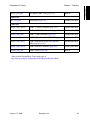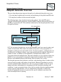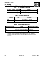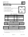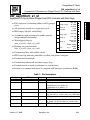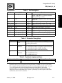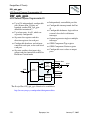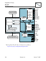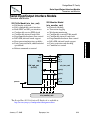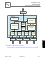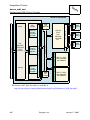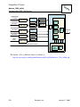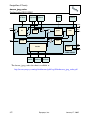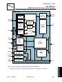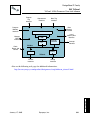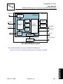
1
DesignWare® IP Family Reference Guide To search the entire manual set, press this toolbar button. For help, refer to intro.pdf. January 17, 2005 DesignWare IP Family Copyright Notice and Proprietary Information Copyright 2005 Synopsys, Inc. All rights reserved. This software and documentation contain confidential and proprietary information that is the property of Synopsys, Inc. The software and documentation are furnished under a license agreement and may be used or copied only in accordance with the terms of the license agreement. No part of the software and documentation may be reproduced, transmitted, or translated, in any form or by any means, electronic, mechanical, manual, optical, or otherwise, without prior written permission of Synopsys, Inc., or as expressly provided by the license agreement. Destination Control Statement All technical data contained in this publication is subject to the export control laws of the United States of America. Disclosure to nationals of other countries contrary to United States law is prohibited. It is the reader’s responsibility to determine the applicable regulations and to comply with them. Disclaimer SYNOPSYS, INC., AND ITS LICENSORS MAKE NO WARRANTY OF ANY KIND, EXPRESS OR IMPLIED, WITH REGARD TO THIS MATERIAL, INCLUDING, BUT NOT LIMITED TO, THE IMPLIED WARRANTIES OF MERCHANTABILITY AND FITNESS FOR A PARTICULAR PURPOSE. Registered Trademarks (®) Synopsys, AMPS, Arcadia, C Level Design, C2HDL, C2V, C2VHDL, Cadabra, Calaveras Algorithm, CATS, COSSAP, CSim, DelayMill, Design Compiler, DesignPower, DesignWare, EPIC, Formality, HSPICE, Hypermodel, I, iN-Phase, InSpecs, in-Sync, Leda, MAST, Meta, Meta-Software, ModelAccess, ModelTools, NanoSim, OpenVera, PathMill, Photolynx, Physical Compiler, PowerMill, PrimeTime, RailMill, Raphael, RapidScript, Saber, SiVL, SmartLogic, SNUG, SolvNet, Stream Driven Simulator, Superlog, System Compiler, Testify, TetraMAX, TimeMill, TMA, VCS, Vera, and Virtual Stepper are registered trademarks of Synopsys, Inc. Trademarks (™) abraCAD, abraMAP, Active Parasitics, AFGen, Apollo, Apollo II, Apollo-DPII, Apollo-GA, ApolloGAII, Astro, Astro-Rail, Astro-Xtalk, Aurora, AvanTestchip, AvanWaves, BCView, Behavioral Compiler, BOA, BRT, Cedar, ChipPlanner, Circuit Analysis, Columbia, Columbia-CE, Comet 3D, Cosmos, CosmosEnterprise, CosmosLE, CosmosScope, CosmosSE, Cyclelink, Davinci, DC Expert, DC Expert Plus, DC Professional, DC Ultra, DC Ultra Plus, Design Advisor, Design Analyzer, Design Vision, DesignerHDL, DesignTime, DFM-Workbench, DFT Compiler, Direct RTL, Direct Silicon Access, DW8051, DWPCI, Dynamic-Macromodeling, Dynamic Model Switcher, ECL Compiler, ECO Compiler, EDAnavigator, Encore, Encore PQ, Evaccess, ExpressModel, Floorplan Manager, Formal Model Checker, FoundryModel, FPGA Compiler II, FPGA Express, Frame Compiler, Galaxy, Gatran, HDL Advisor, HDL Compiler, Hercules, Hercules-Explorer, Hercules-II, Hierarchical Optimization Technology, High Performance Option, HotPlace, HSPICE-Link, iN-Tandem, Integrator, Interactive Waveform Viewer, i-Virtual Stepper, Jupiter, Jupiter-DP, JupiterXT, JupiterXT-ASIC, JVXtreme, Liberty, Libra-Passport, Library Compiler, Libra-Visa, LRC, Magellan, Mars, Mars-Rail, Mars-Xtalk, Medici, Metacapture, Metacircuit, Metamanager, Metamixsim, Milkyway, ModelSource, Module Compiler, MS-3200, MS-3400, Nova Product Family, Nova-ExploreRTL, Nova-Trans, Nova-VeriLint, Nova-VHDLlint, Optimum Silicon, Orion_ec, Parasitic View, Passport, Planet, Planet-PL, Planet-RTL, Polaris, Polaris-CBS, Polaris-MT, Power Compiler, PowerCODE, PowerGate, ProFPGA, Progen, Prospector, Proteus OPC, Protocol Compiler, PSMGen, Raphael-NES, RoadRunner, RTL Analyzer, Saturn, ScanBand, Schematic Compiler, Scirocco, Scirocco-i, Shadow Debugger, Silicon Blueprint, Silicon Early Access, SinglePass-SoC, Smart Extraction, SmartLicense, SmartModel Library, Softwire, Source-Level Design, Star, Star-DC, Star-MS, Star-MTB, Star-Power, Star-Rail, Star-RC, Star-RCXT, Star-Sim, Star-SimXT, Star-Time, Star-XP, SWIFT, Taurus, Taurus-Device, Taurus-Layout, Taurus-Lithography, Taurus-OPC, Taurus-Process, Taurus-Topography, Taurus-Visual, Taurus-Workbench, TimeSlice, TimeTracker, Timing Annotator, TopoPlace, TopoRoute, Trace-On-Demand, True-Hspice, TSUPREM-4, TymeWare, VCS Express, VCSi, Venus, Verification Portal, VFormal, VHDL Compiler, VHDL System Simulator, VirSim, and VMC are trademarks of Synopsys, Inc. Service Marks (SM) MAP-in, SVP Café, and TAP-in are service marks of Synopsys, Inc. SystemC is a trademark of the Open SystemC Initiative and is used under license. AMBA is a trademark of ARM Limited. ARM is a registered trademark of ARM Limited. All other product or company names may be trademarks of their respective owners. 2 Synopsys, Inc. January 17, 2005 DesignWare IP Family Contents Contents Preface . . . . . . . . . . . . . . . . . . . . . . . . . . . . . . . . . . . . . . . . . . . . . . . . . . . . . . . . . . . . . 15 About This Manual . . . . . . . . . . . . . . . . . . . . . . . . . . . . . . . . . . . . . . . . . . . . . . . . . . . . . . . Manual Overview . . . . . . . . . . . . . . . . . . . . . . . . . . . . . . . . . . . . . . . . . . . . . . . . . . . . . Typographical and Symbol Conventions . . . . . . . . . . . . . . . . . . . . . . . . . . . . . . . . . . . Synopsys Common Licensing (SCL) . . . . . . . . . . . . . . . . . . . . . . . . . . . . . . . . . . . . . . . . . Getting Help . . . . . . . . . . . . . . . . . . . . . . . . . . . . . . . . . . . . . . . . . . . . . . . . . . . . . . . . . . . . Additional Information . . . . . . . . . . . . . . . . . . . . . . . . . . . . . . . . . . . . . . . . . . . . . . . . . Comments? . . . . . . . . . . . . . . . . . . . . . . . . . . . . . . . . . . . . . . . . . . . . . . . . . . . . . . . . . . . . . 15 15 16 16 17 17 17 Chapter 1 Overview . . . . . . . . . . . . . . . . . . . . . . . . . . . . . . . . . . . . . . . . . . . . . . . . . . . . . . . . . . . 19 DesignWare Library . . . . . . . . . . . . . . . . . . . . . . . . . . . . . . . . . . . . . . . . . . . . . . . . . . . . . . Building Block IP . . . . . . . . . . . . . . . . . . . . . . . . . . . . . . . . . . . . . . . . . . . . . . . . . . . . . AMBA On-Chip Bus . . . . . . . . . . . . . . . . . . . . . . . . . . . . . . . . . . . . . . . . . . . . . . . . . . Star IP Microprocessor and DSP Cores . . . . . . . . . . . . . . . . . . . . . . . . . . . . . . . . . . . . Microcontrollers . . . . . . . . . . . . . . . . . . . . . . . . . . . . . . . . . . . . . . . . . . . . . . . . . . . . . . Memory IP . . . . . . . . . . . . . . . . . . . . . . . . . . . . . . . . . . . . . . . . . . . . . . . . . . . . . . . . . . Foundry Libraries . . . . . . . . . . . . . . . . . . . . . . . . . . . . . . . . . . . . . . . . . . . . . . . . . . . . . Verification IP for Bus and I/O Standards . . . . . . . . . . . . . . . . . . . . . . . . . . . . . . . . . . Board Verification IP . . . . . . . . . . . . . . . . . . . . . . . . . . . . . . . . . . . . . . . . . . . . . . . . . . DesignWare Verification Library . . . . . . . . . . . . . . . . . . . . . . . . . . . . . . . . . . . . . . . . . . . . DesignWare Cores . . . . . . . . . . . . . . . . . . . . . . . . . . . . . . . . . . . . . . . . . . . . . . . . . . . . . . . DesignWare Star IP . . . . . . . . . . . . . . . . . . . . . . . . . . . . . . . . . . . . . . . . . . . . . . . . . . . . . . . 20 21 22 23 24 24 24 25 26 26 28 30 Chapter 2 DesignWare Library Synthesizable IP . . . . . . . . . . . . . . . . . . . . . . . . . . . . . . . . . . . . . . . . . . . . . . . . . . . . . 31 Building Block IP . . . . . . . . . . . . . . . . . . . . . . . . . . . . . . . . . . . . . . . . . . . . . . . . . . . . . . . 31 Building Block IP for DC QuickStart . . . . . . . . . . . . . . . . . . . . . . . . . . . . . . . . . . . . . . 32 Building Block IP in DC-FPGA QuickStart . . . . . . . . . . . . . . . . . . . . . . . . . . . . . . . . . 34 Building Block IP in FPGA Compiler II QuickStart . . . . . . . . . . . . . . . . . . . . . . . . . . 36 Application Specific – Control Logic . . . . . . . . . . . . . . . . . . . . . . . . . . . . . . . . . . . . . . 38 DW_arbiter_2t Two-Tier Arbiter with Dynamic/Fair-Among-Equal Scheme . . . . . . . . . . . . . . . . 39 DW_arbiter_dp Arbiter with Dynamic Priority Scheme . . . . . . . . . . . . . . . . . . . . . . . . . . . . . . . . . 41 DW_arbiter_fcfs Arbiter with First-Come-First-Served Priority Scheme . . . . . . . . . . . . . . . . . . . . . 43 DW_arbiter_sp Arbiter with Static Priority Scheme . . . . . . . . . . . . . . . . . . . . . . . . . . . . . . . . . . . . 45 January 17, 2005 Synopsys, Inc. 3 Contents DesignWare IP Family Application Specific – Interface Overview . . . . . . . . . . . . . . . . . . . . . . . . . . . . . . . . . . 47 DW_debugger On-Chip ASCII Debugger . . . . . . . . . . . . . . . . . . . . . . . . . . . . . . . . . . . . . . . . . . . 48 Datapath Generator Overview . . . . . . . . . . . . . . . . . . . . . . . . . . . . . . . . . . . . . . . . . . . 50 Datapath – Arithmetic Overview . . . . . . . . . . . . . . . . . . . . . . . . . . . . . . . . . . . . . . . . . 51 DW01_absval Absolute Value . . . . . . . . . . . . . . . . . . . . . . . . . . . . . . . . . . . . . . . . . . . . . . . . . . . . 52 DW01_add Adder . . . . . . . . . . . . . . . . . . . . . . . . . . . . . . . . . . . . . . . . . . . . . . . . . . . . . . . . . . . 53 DW01_addsub Adder-Subtractor . . . . . . . . . . . . . . . . . . . . . . . . . . . . . . . . . . . . . . . . . . . . . . . . . . 55 DW_addsub_dx Duplex Adder/Subtractor with Saturation and Rounding . . . . . . . . . . . . . . . . . . . 57 DW01_ash Arithmetic Shifter . . . . . . . . . . . . . . . . . . . . . . . . . . . . . . . . . . . . . . . . . . . . . . . . . . 59 DW_bin2gray Binary to Gray Converter . . . . . . . . . . . . . . . . . . . . . . . . . . . . . . . . . . . . . . . . . . . . 61 DW01_bsh Barrel Shifter . . . . . . . . . . . . . . . . . . . . . . . . . . . . . . . . . . . . . . . . . . . . . . . . . . . . . 62 DW01_cmp2 2-Function Comparator . . . . . . . . . . . . . . . . . . . . . . . . . . . . . . . . . . . . . . . . . . . . . 63 DW01_cmp6 6-Function Comparator . . . . . . . . . . . . . . . . . . . . . . . . . . . . . . . . . . . . . . . . . . . . . 65 DW_cmp_dx Duplex Comparator . . . . . . . . . . . . . . . . . . . . . . . . . . . . . . . . . . . . . . . . . . . . . . . . 67 DW_cntr_gray Gray Code Counter . . . . . . . . . . . . . . . . . . . . . . . . . . . . . . . . . . . . . . . . . . . . . . . . . 69 DW01_csa Carry Save Adder . . . . . . . . . . . . . . . . . . . . . . . . . . . . . . . . . . . . . . . . . . . . . . . . . . 70 DW01_dec Decrementer . . . . . . . . . . . . . . . . . . . . . . . . . . . . . . . . . . . . . . . . . . . . . . . . . . . . . . 71 DW_div Combinational Divider . . . . . . . . . . . . . . . . . . . . . . . . . . . . . . . . . . . . . . . . . . . . . . 73 DW_div_pipe Stallable Pipelined Divider . . . . . . . . . . . . . . . . . . . . . . . . . . . . . . . . . . . . . . . . . . . 75 DW_gray2bin Gray-to-Binary Converter . . . . . . . . . . . . . . . . . . . . . . . . . . . . . . . . . . . . . . . . . . . 77 DW01_inc Incrementer . . . . . . . . . . . . . . . . . . . . . . . . . . . . . . . . . . . . . . . . . . . . . . . . . . . . . . . 78 DW01_incdec Incrementer-Decrementer . . . . . . . . . . . . . . . . . . . . . . . . . . . . . . . . . . . . . . . . . . . . 80 DW_inc_gray Gray Incrementer . . . . . . . . . . . . . . . . . . . . . . . . . . . . . . . . . . . . . . . . . . . . . . . . . . 82 DW02_mac Multiplier-Accumulator . . . . . . . . . . . . . . . . . . . . . . . . . . . . . . . . . . . . . . . . . . . . . 83 4 Synopsys, Inc. January 17, 2005 DesignWare IP Family Contents DW_minmax Minimum/Maximum Value . . . . . . . . . . . . . . . . . . . . . . . . . . . . . . . . . . . . . . . . . . 85 DW02_mult Multiplier . . . . . . . . . . . . . . . . . . . . . . . . . . . . . . . . . . . . . . . . . . . . . . . . . . . . . . . . 86 DW02_multp Partial Product Multiplier . . . . . . . . . . . . . . . . . . . . . . . . . . . . . . . . . . . . . . . . . . . . 88 DW02_mult_2_stage Two-Stage Pipelined Multiplier . . . . . . . . . . . . . . . . . . . . . . . . . . . . . . . . . . . . . . . 90 DW02_mult_3_stage Three-Stage Pipelined Multiplier . . . . . . . . . . . . . . . . . . . . . . . . . . . . . . . . . . . . . . 92 DW02_mult_4_stage Four-Stage Pipelined Multiplier . . . . . . . . . . . . . . . . . . . . . . . . . . . . . . . . . . . . . . . 93 DW02_mult_5_stage Five-Stage Pipelined Multiplier . . . . . . . . . . . . . . . . . . . . . . . . . . . . . . . . . . . . . . . 94 DW02_mult_6_stage Six-Stage Pipelined Multiplier . . . . . . . . . . . . . . . . . . . . . . . . . . . . . . . . . . . . . . . . 96 DW_mult_dx Duplex Multiplier . . . . . . . . . . . . . . . . . . . . . . . . . . . . . . . . . . . . . . . . . . . . . . . . . . 98 DW_mult_pipe Stallable Pipelined multiplier . . . . . . . . . . . . . . . . . . . . . . . . . . . . . . . . . . . . . . . . . 99 DW02_prod_sum Generalized Sum of Products . . . . . . . . . . . . . . . . . . . . . . . . . . . . . . . . . . . . . . . . 101 DW02_prod_sum1 Multiplier-Adder . . . . . . . . . . . . . . . . . . . . . . . . . . . . . . . . . . . . . . . . . . . . . . . . . 103 DW_prod_sum_pipe Stallable Pipelined Generalized Sum of Products . . . . . . . . . . . . . . . . . . . . . . . . 105 DW01_satrnd Arithmetic Saturation and Rounding Logic . . . . . . . . . . . . . . . . . . . . . . . . . . . . . 107 DW_shifter Combined Arithmetic and Barrel Shifter . . . . . . . . . . . . . . . . . . . . . . . . . . . . . . . 109 DW_square Integer Squarer . . . . . . . . . . . . . . . . . . . . . . . . . . . . . . . . . . . . . . . . . . . . . . . . . . . 111 DW_squarep Partial Product Integer Squarer . . . . . . . . . . . . . . . . . . . . . . . . . . . . . . . . . . . . . . 113 DW_sqrt Combinational Square Root . . . . . . . . . . . . . . . . . . . . . . . . . . . . . . . . . . . . . . . . . 114 DW_sqrt_pipe Stallable Pipelined square root . . . . . . . . . . . . . . . . . . . . . . . . . . . . . . . . . . . . . . . 115 DW01_sub Subtractor . . . . . . . . . . . . . . . . . . . . . . . . . . . . . . . . . . . . . . . . . . . . . . . . . . . . . . . 117 DW02_sum Vector Adder . . . . . . . . . . . . . . . . . . . . . . . . . . . . . . . . . . . . . . . . . . . . . . . . . . . . 119 DW02_tree Wallace Tree Compressor . . . . . . . . . . . . . . . . . . . . . . . . . . . . . . . . . . . . . . . . . . . 121 Datapath – Floating Point Overview . . . . . . . . . . . . . . . . . . . . . . . . . . . . . . . . . . . . . . 122 January 17, 2005 Synopsys, Inc. 5 Contents DesignWare IP Family DW_i2flt_fp Integer-to-Floating Point Converter . . . . . . . . . . . . . . . . . . . . . . . . . . . . . . . . . . . 123 DW_add_fp Floating Point Adder . . . . . . . . . . . . . . . . . . . . . . . . . . . . . . . . . . . . . . . . . . . . . . 124 DW_cmp_fp Floating Point Comparator . . . . . . . . . . . . . . . . . . . . . . . . . . . . . . . . . . . . . . . . . . 125 DW_div_fp Floating Point Divider . . . . . . . . . . . . . . . . . . . . . . . . . . . . . . . . . . . . . . . . . . . . . 126 DW_mult_fp Floating Point Multiplier . . . . . . . . . . . . . . . . . . . . . . . . . . . . . . . . . . . . . . . . . . . 128 DW_flt2i_fp Floating Point-to-Integer Converter . . . . . . . . . . . . . . . . . . . . . . . . . . . . . . . . . . . 129 Datapath – Sequential Overview . . . . . . . . . . . . . . . . . . . . . . . . . . . . . . . . . . . . . . . . . 130 DW_div_seq Sequential Divider . . . . . . . . . . . . . . . . . . . . . . . . . . . . . . . . . . . . . . . . . . . . . . . . 131 DW_mult_seq Sequential Multiplier . . . . . . . . . . . . . . . . . . . . . . . . . . . . . . . . . . . . . . . . . . . . . . 133 DW_sqrt_seq Sequential Square Root . . . . . . . . . . . . . . . . . . . . . . . . . . . . . . . . . . . . . . . . . . . . 135 Datapath – Trigonometric Overview . . . . . . . . . . . . . . . . . . . . . . . . . . . . . . . . . . . . . 137 DW02_cos Combinational Cosine . . . . . . . . . . . . . . . . . . . . . . . . . . . . . . . . . . . . . . . . . . . . . 138 DW02_sin Combinational Sine . . . . . . . . . . . . . . . . . . . . . . . . . . . . . . . . . . . . . . . . . . . . . . . 139 DW02_sincos Combinational Sine - Cosine . . . . . . . . . . . . . . . . . . . . . . . . . . . . . . . . . . . . . . . . 140 Data Integrity . . . . . . . . . . . . . . . . . . . . . . . . . . . . . . . . . . . . . . . . . . . . . . . . . . . . . . . 141 DW_crc_p Universal Parallel (Combinational) CRC Generator/Checker . . . . . . . . . . . . . . . 142 DW_crc_s Universal Synchronous (Clocked) CRC Generator/Checker . . . . . . . . . . . . . . . . 144 DW_ecc Error Checking and Correction . . . . . . . . . . . . . . . . . . . . . . . . . . . . . . . . . . . . . . 146 DW04_par_gen Parity Generator and Checker . . . . . . . . . . . . . . . . . . . . . . . . . . . . . . . . . . . . . . . 148 Data Integrity – Coding Group Overview . . . . . . . . . . . . . . . . . . . . . . . . . . . . . . . . . . 149 DW_8b10b_dec 8b10b Decoder . . . . . . . . . . . . . . . . . . . . . . . . . . . . . . . . . . . . . . . . . . . . . . . . . . . 150 DW_8b10b_enc 8b10b Encoder . . . . . . . . . . . . . . . . . . . . . . . . . . . . . . . . . . . . . . . . . . . . . . . . . . . 152 DW_8b10b_unbal 8b10b Coding Balance Predictor . . . . . . . . . . . . . . . . . . . . . . . . . . . . . . . . . . . . . 154 Digital Signal Processing (DSP) . . . . . . . . . . . . . . . . . . . . . . . . . . . . . . . . . . . . . . . . . 155 DW_fir High-Speed Digital FIR Filter . . . . . . . . . . . . . . . . . . . . . . . . . . . . . . . . . . . . . . . 156 6 Synopsys, Inc. January 17, 2005 DesignWare IP Family Contents DW_fir_seq Sequential Digital FIR Filter . . . . . . . . . . . . . . . . . . . . . . . . . . . . . . . . . . . . . . . . 158 DW_iir_dc High-Speed Digital IIR Filter with Dynamic Coefficients . . . . . . . . . . . . . . . . . . 160 DW_iir_sc High-Speed Digital IIR Filter with Static Coefficients . . . . . . . . . . . . . . . . . . . . 163 Logic – Combinational Overview . . . . . . . . . . . . . . . . . . . . . . . . . . . . . . . . . . . . . . . . 165 DW01_binenc Binary Encoder . . . . . . . . . . . . . . . . . . . . . . . . . . . . . . . . . . . . . . . . . . . . . . . . . . . 166 DW01_decode Decoder . . . . . . . . . . . . . . . . . . . . . . . . . . . . . . . . . . . . . . . . . . . . . . . . . . . . . . . . 167 DW01_mux_any Universal Multiplexer . . . . . . . . . . . . . . . . . . . . . . . . . . . . . . . . . . . . . . . . . . . . . . 168 DW01_prienc Priority Encoder . . . . . . . . . . . . . . . . . . . . . . . . . . . . . . . . . . . . . . . . . . . . . . . . . . 169 Logic – Sequential Overview . . . . . . . . . . . . . . . . . . . . . . . . . . . . . . . . . . . . . . . . . . . 170 DW03_bictr_dcnto Up/Down Binary Counter with Dynamic Count-to Flag . . . . . . . . . . . . . . . . . . . 171 DW03_bictr_scnto Up/Down Binary Counter with Static Count-to Flag . . . . . . . . . . . . . . . . . . . . . . 172 DW03_bictr_decode Up/Down Binary Counter with Output Decode . . . . . . . . . . . . . . . . . . . . . . . . . . 173 DW_dpll_sd Digital Phase Locked Loop . . . . . . . . . . . . . . . . . . . . . . . . . . . . . . . . . . . . . . . . . 174 DW03_lfsr_dcnto LFSR Counter with Dynamic Count-to Flag . . . . . . . . . . . . . . . . . . . . . . . . . . . . 176 DW03_lfsr_scnto LFSR Counter with Static Count-to Flag . . . . . . . . . . . . . . . . . . . . . . . . . . . . . . . 177 DW03_lfsr_load LFSR Counter with Loadable Input . . . . . . . . . . . . . . . . . . . . . . . . . . . . . . . . . . . 178 DW03_lfsr_updn LFSR Up/Down Counter . . . . . . . . . . . . . . . . . . . . . . . . . . . . . . . . . . . . . . . . . . . 179 DW03_updn_ctr Up/Down Counter . . . . . . . . . . . . . . . . . . . . . . . . . . . . . . . . . . . . . . . . . . . . . . . . 180 Memory – FIFO Overview . . . . . . . . . . . . . . . . . . . . . . . . . . . . . . . . . . . . . . . . . . . . . 181 DW_asymfifo_s1_df Asymmetric I/O Synchronous (Single Clock) FIFO with Dynamic Flag . . . . . . 182 DW_asymfifo_s1_sf Asymmetric I/O Synchronous (Single Clock) FIFO with Static Flags . . . . . . . . 185 DW_asymfifo_s2_sf Asymmetric Synchronous (Dual Clock) FIFO with Static Flags . . . . . . . . . . . . . 189 DW_fifo_s1_df Synchronous (Single Clock) FIFO with Dynamic Flags . . . . . . . . . . . . . . . . . . . 193 DW_fifo_s1_sf Synchronous (Single Clock) FIFO with Static Flags . . . . . . . . . . . . . . . . . . . . . . 195 January 17, 2005 Synopsys, Inc. 7 Contents DesignWare IP Family DW_fifo_s2_sf Synchronous (Dual-Clock) FIFO with Static Flags . . . . . . . . . . . . . . . . . . . . . . . 197 DW_asymfifoctl_s1_df Asymmetric I/O Synchronous (Single Clock) FIFO Controller with Dynamic Flags 200 DW_asymfifoctl_s1_sf Asymmetric I/O Synchronous (Single Clock) FIFO Controller with Static Flags . . 203 DW_asymfifoctl_s2_sf Asymmetric Synchronous (Dual-Clock) FIFO Controller with Static Flags . . . . 206 DW_fifoctl_s1_df DW_fifoctl_s1_sf Synchronous (SingleClock) FIFO Controller with Static Flags . . . . . . . . . . . . . . 212 DW_fifoctl_s2_sf Synchronous (Dual Clock) FIFO Controller with Static Flags . . . . . . . . . . . . . . 214 Memory – Registers . . . . . . . . . . . . . . . . . . . . . . . . . . . . . . . . . . . . . . . . . . . . . . . . . . 217 DW03_pipe_reg Pipeline Register . . . . . . . . . . . . . . . . . . . . . . . . . . . . . . . . . . . . . . . . . . . . . . . . . 218 DW03_reg_s_pl Register with Synchronous Enable Reset . . . . . . . . . . . . . . . . . . . . . . . . . . . . . . . 219 DW04_shad_reg Shadow and Multibit Register . . . . . . . . . . . . . . . . . . . . . . . . . . . . . . . . . . . . . . . 220 DW03_shftreg Shift Register . . . . . . . . . . . . . . . . . . . . . . . . . . . . . . . . . . . . . . . . . . . . . . . . . . . . 222 Memory – Synchronous RAMs . . . . . . . . . . . . . . . . . . . . . . . . . . . . . . . . . . . . . . . . . 223 DW_ram_r_w_s_dff Synchronous Write-Port, Asynchronous Read-Port RAM (Flip-Flop-Based) . . . 224 DW_ram_r_w_s_lat Synchronous Write Port, Asynchronous Read Port RAM (Latch-Based) . . . . . . 225 DW_ram_2r_w_s_dff Synchronous Write Port, Asynchronous Dual Read Port RAM (Flip-Flop-Based) . 226 DW_ram_2r_w_s_lat Synchronous Write Port, Asynchronous Dual Read Port RAM (Latch-Based) . 228 DW_ram_rw_s_dff Synchronous Single Port Read/Write RAM (Flip-Flop-Based) . . . . . . . . . . . . . . 229 DW_ram_rw_s_lat Synchronous Single Port Read/Write RAM (Latch-Based) . . . . . . . . . . . . . . . . . 230 Memory – Asynchronous RAMs . . . . . . . . . . . . . . . . . . . . . . . . . . . . . . . . . . . . . . . . 231 DW_ram_r_w_a_dff Asynchronous Dual Port RAM (Flip-Flop-Based) . . . . . . . . . . . . . . . . . . . . . . . 232 DW_ram_r_w_a_lat Asynchronous Dual Port RAM (Latch-Based) . . . . . . . . . . . . . . . . . . . . . . . . . . 233 DW_ram_2r_w_a_dff Write Port, Dual Read Port RAM (Flip-Flop-Based) . . . . . . . . . . . . . . . . . . . . . 234 8 Synopsys, Inc. January 17, 2005 DesignWare IP Family Contents DW_ram_2r_w_a_lat Write Port, Dual Read Port RAM (Latch-Based) . . . . . . . . . . . . . . . . . . . . . . . . 236 DW_ram_rw_a_dff Asynchronous Single Port RAM (Flip-Flop-Based) . . . . . . . . . . . . . . . . . . . . . . 237 DW_ram_rw_a_lat Asynchronous Single-Port RAM (Latch-Based) . . . . . . . . . . . . . . . . . . . . . . . . . 238 Memory – Stacks . . . . . . . . . . . . . . . . . . . . . . . . . . . . . . . . . . . . . . . . . . . . . . . . . . . . 239 DW_stack Synchronous (Single-Clock) Stack . . . . . . . . . . . . . . . . . . . . . . . . . . . . . . . . . . . 240 DW_stackctl Synchronous (Single-Clock) Stack Controller . . . . . . . . . . . . . . . . . . . . . . . . . . . 242 Test – JTAG Overview . . . . . . . . . . . . . . . . . . . . . . . . . . . . . . . . . . . . . . . . . . . . . . . . 244 DW_tap TAP Controller . . . . . . . . . . . . . . . . . . . . . . . . . . . . . . . . . . . . . . . . . . . . . . . . . . . 245 DW_tap_uc TAP Controller with USERCODE support . . . . . . . . . . . . . . . . . . . . . . . . . . . . . 247 DW_bc_1 Boundary Scan Cell Type BC_1 . . . . . . . . . . . . . . . . . . . . . . . . . . . . . . . . . . . . . 250 DW_bc_2 Boundary Scan Cell Type BC_2 . . . . . . . . . . . . . . . . . . . . . . . . . . . . . . . . . . . . . 251 DW_bc_3 Boundary Scan Cell Type BC_3 . . . . . . . . . . . . . . . . . . . . . . . . . . . . . . . . . . . . . 252 DW_bc_4 Boundary Scan Cell Type BC_4 . . . . . . . . . . . . . . . . . . . . . . . . . . . . . . . . . . . . . 253 DW_bc_5 Boundary Scan Cell Type BC_5 . . . . . . . . . . . . . . . . . . . . . . . . . . . . . . . . . . . . . 254 DW_bc_7 Boundary Scan Cell Type BC_7 . . . . . . . . . . . . . . . . . . . . . . . . . . . . . . . . . . . . . 255 DW_bc_8 Boundary Scan Cell Type BC_8 . . . . . . . . . . . . . . . . . . . . . . . . . . . . . . . . . . . . . 257 DW_bc_9 Boundary Scan Cell Type BC_9 . . . . . . . . . . . . . . . . . . . . . . . . . . . . . . . . . . . . . 259 DW_bc_10 Boundary Scan Cell Type BC_10 . . . . . . . . . . . . . . . . . . . . . . . . . . . . . . . . . . . . 261 GTECH Library Overview . . . . . . . . . . . . . . . . . . . . . . . . . . . . . . . . . . . . . . . . . . . . . 263 AMBA Bus Fabric and Peripherals IP . . . . . . . . . . . . . . . . . . . . . . . . . . . . . . . . . . . . . . . 264 DW_ahb Advanced High-Performance Bus . . . . . . . . . . . . . . . . . . . . . . . . . . . . . . . . . . . . 266 DW_ahb_dmac AHB Central Direct Memory Access (DMA) Controller . . . . . . . . . . . . . . . . . . 268 DW_ahb_eh2h Enhanced AHB to AHB Bridge . . . . . . . . . . . . . . . . . . . . . . . . . . . . . . . . . . . . . . 269 DW_ahb_icm AHB Multi-layer Interconnection Matrix . . . . . . . . . . . . . . . . . . . . . . . . . . . . . . 271 DW_ahb_ictl January 17, 2005 Synopsys, Inc. 9 Contents DesignWare IP Family AHB Interrupt Controller . . . . . . . . . . . . . . . . . . . . . . . . . . . . . . . . . . . . . . . . . . . 272 DW_apb Advanced Peripheral Bus . . . . . . . . . . . . . . . . . . . . . . . . . . . . . . . . . . . . . . . . . . . 273 DW_apb_gpio APB General Purpose Programmable I/O . . . . . . . . . . . . . . . . . . . . . . . . . . . . . . 274 DW_apb_i2c APB I2C Interface . . . . . . . . . . . . . . . . . . . . . . . . . . . . . . . . . . . . . . . . . . . . . . . . 275 DW_apb_ictl APB Interrupt Controller . . . . . . . . . . . . . . . . . . . . . . . . . . . . . . . . . . . . . . . . . . . 276 DW_apb_rap APB Remap and Pause . . . . . . . . . . . . . . . . . . . . . . . . . . . . . . . . . . . . . . . . . . . . . 277 DW_apb_rtc APB Real Time Clock . . . . . . . . . . . . . . . . . . . . . . . . . . . . . . . . . . . . . . . . . . . . . 278 DW_apb_ssi APB Synchronous Serial Interface . . . . . . . . . . . . . . . . . . . . . . . . . . . . . . . . . . . . 279 DW_apb_timers APB Programmable Timers . . . . . . . . . . . . . . . . . . . . . . . . . . . . . . . . . . . . . . . . . 281 DW_apb_uart APB Universal Asynchronous Receiver/Transmitter . . . . . . . . . . . . . . . . . . . . . . 282 DW_ahb_h2h AHB to AHB Bridge . . . . . . . . . . . . . . . . . . . . . . . . . . . . . . . . . . . . . . . . . . . . . . 284 DW_apb_wdt APB Watchdog Timer . . . . . . . . . . . . . . . . . . . . . . . . . . . . . . . . . . . . . . . . . . . . . 286 DesignWare AMBA Connect Design environment for AMBA synthesizable and verification IP . . . . . . . . . . . 287 DesignWare AMBA QuickStart Collection of example designs for AMBA subsystems . . . . . . . . . . . . . . . . . . . . 288 Memory IP . . . . . . . . . . . . . . . . . . . . . . . . . . . . . . . . . . . . . . . . . . . . . . . . . . . . . . . . . . . . 291 DW_memctl Memory Controller . . . . . . . . . . . . . . . . . . . . . . . . . . . . . . . . . . . . . . . . . . . . . . . . 292 DW_rambist Memory Built-In Self Test . . . . . . . . . . . . . . . . . . . . . . . . . . . . . . . . . . . . . . . . . . 294 Microprocessors/Microcontrollers . . . . . . . . . . . . . . . . . . . . . . . . . . . . . . . . . . . . . . . . . . 296 DW_6811 6811 Microcontroller . . . . . . . . . . . . . . . . . . . . . . . . . . . . . . . . . . . . . . . . . . . . . . 297 DW8051 8051 Microcontroller . . . . . . . . . . . . . . . . . . . . . . . . . . . . . . . . . . . . . . . . . . . . . . 299 Chapter 3 DesignWare Library Verification IP . . . . . . . . . . . . . . . . . . . . . . . . . . . . . . . . . . . . 301 Overview . . . . . . . . . . . . . . . . . . . . . . . . . . . . . . . . . . . . . . . . . . . . . . . . . . . . . . . . . . . . . . 301 Verification Models . . . . . . . . . . . . . . . . . . . . . . . . . . . . . . . . . . . . . . . . . . . . . . . . . . . . . . 303 DesignWare AMBA AHB Models Master, Slave, Monitor, Bus Interconnect . . . . . . . . . . . . . . . . . . . . . . . . . . . . . . 304 DesignWare AMBA APB Models 10 Synopsys, Inc. January 17, 2005 DesignWare IP Family Contents Master, Slave, Monitor . . . . . . . . . . . . . . . . . . . . . . . . . . . . . . . . . . . . . . . . . . . . . 306 DesignWare VIP for AMBA 3 AXI Master, Slave, Monitor, Interconnect . . . . . . . . . . . . . . . . . . . . . . . . . . . . . . . . . . 307 Board Verification IP Simulation models for Board Verification . . . . . . . . . . . . . . . . . . . . . . . . . . . . . . 309 Ethernet (10, 100, 1G, 10G) Models Transceiver and Monitor . . . . . . . . . . . . . . . . . . . . . . . . . . . . . . . . . . . . . . . . . . . 310 Ethernet Models RMII Transceiver and Hub . . . . . . . . . . . . . . . . . . . . . . . . . . . . . . . . . . . . . . . . . . 311 2 I C Models Transceiver and Monitor . . . . . . . . . . . . . . . . . . . . . . . . . . . . . . . . . . . . . . . . . . . 312 Memory Models Simulation models of memory devices . . . . . . . . . . . . . . . . . . . . . . . . . . . . . . . . 313 PCI Express Models Transceiver and Monitor . . . . . . . . . . . . . . . . . . . . . . . . . . . . . . . . . . . . . . . . . . . 314 PCI / PCI-X Bus Models Master, Slave, and Monitor . . . . . . . . . . . . . . . . . . . . . . . . . . . . . . . . . . . . . . . . . 316 Serial ATA Models -- PRELIMINARY Device and Monitor . . . . . . . . . . . . . . . . . . . . . . . . . . . . . . . . . . . . . . . . . . . . . . . 317 Serial Input/Output Interface Models Tranceiver and Monitor . . . . . . . . . . . . . . . . . . . . . . . . . . . . . . . . . . . . . . . . . . . . 318 USB On-The-Go Models Host, Device, and Monitor . . . . . . . . . . . . . . . . . . . . . . . . . . . . . . . . . . . . . . . . . . 319 DesignWare VMT Models . . . . . . . . . . . . . . . . . . . . . . . . . . . . . . . . . . . . . . . . . . . . . . . . 320 DesignWare FlexModels . . . . . . . . . . . . . . . . . . . . . . . . . . . . . . . . . . . . . . . . . . . . . . . . . 322 Listing of FlexModels . . . . . . . . . . . . . . . . . . . . . . . . . . . . . . . . . . . . . . . . . . . . . . . . . 322 DesignWare SmartModels . . . . . . . . . . . . . . . . . . . . . . . . . . . . . . . . . . . . . . . . . . . . . . . . 324 SmartModel Features . . . . . . . . . . . . . . . . . . . . . . . . . . . . . . . . . . . . . . . . . . . . . . . . . 324 SmartModel Types . . . . . . . . . . . . . . . . . . . . . . . . . . . . . . . . . . . . . . . . . . . . . . . . . . . 324 SmartModel Timing Definitions . . . . . . . . . . . . . . . . . . . . . . . . . . . . . . . . . . . . . . . . . 325 Specific Model Information . . . . . . . . . . . . . . . . . . . . . . . . . . . . . . . . . . . . . . . . . . . . 325 Chapter 4 DesignWare Foundry Libraries . . . . . . . . . . . . . . . . . . . . . . . . . . . . . . . . . . . . . . . . 326 TSMC Libraries . . . . . . . . . . . . . . . . . . . . . . . . . . . . . . . . . . . . . . . . . . . . . . . . . . . . . . . . 326 Tower Libraries . . . . . . . . . . . . . . . . . . . . . . . . . . . . . . . . . . . . . . . . . . . . . . . . . . . . . . . . . 329 Chapter 5 DesignWare Cores . . . . . . . . . . . . . . . . . . . . . . . . . . . . . . . . . . . . . . . . . . . . . . . . . . . 330 dwcore_ethernet Synthesizable Ethernet Core . . . . . . . . . . . . . . . . . . . . . . . . . . . . . . . . . . . . . . . . 333 dwcore_ethernet_sub Synthesizable Ethernet Subsystem . . . . . . . . . . . . . . . . . . . . . . . . . . . . . . . . . . . . 335 dwcore_gig_ethernet Synthesizable Gigabit Ethernet Core . . . . . . . . . . . . . . . . . . . . . . . . . . . . . . . . . . 337 January 17, 2005 Synopsys, Inc. 11 Contents DesignWare IP Family dwcore_gig_ethernet_sub Synthesizable Gigabit Ethernet Subsystem . . . . . . . . . . . . . . . . . . . . . . . . . . . . . 339 dwcore_pci Synthesizable Universal PCI Controller . . . . . . . . . . . . . . . . . . . . . . . . . . . . . . . . 341 dwcore_pcix Synthesizable PCI-X Controller and Test Environment . . . . . . . . . . . . . . . . . . . . 343 dwc_pcie_endpoint PCI Express Endpoint Synthesizable Core . . . . . . . . . . . . . . . . . . . . . . . . . . . . . 345 dwc_pcie_rootport PCI Express Root Port Synthesizable Core . . . . . . . . . . . . . . . . . . . . . . . . . . . . . 347 dwc_pcie_switchport PCI Express Switch Port Synthesizable Core . . . . . . . . . . . . . . . . . . . . . . . . . . . 349 dwc_pcie_dualmode PCI Express RC/EP Dual Mode Synthesizable Core . . . . . . . . . . . . . . . . . . . . . . 350 dwcore_pcie_phy PCI Express PHY Core . . . . . . . . . . . . . . . . . . . . . . . . . . . . . . . . . . . . . . . . . . . . 352 dwcore_sd_mmc_host Secure Digital (SD) and Multimedia Card (MMC) Host Controller . . . . . . . . . . 353 dwcore_usb1_device Synthesizable USB 1.1 Device Controller . . . . . . . . . . . . . . . . . . . . . . . . . . . . . . 355 dwcore_usb1_host Synthesizable USB 1.1 OHCI Host Controller . . . . . . . . . . . . . . . . . . . . . . . . . . 357 dwcore_usb1_hub Synthesizable USB 1.1 Hub Controller . . . . . . . . . . . . . . . . . . . . . . . . . . . . . . . . 359 dwcore_usb2_hsotg Synthesizable USB 2.0 Hi-Speed On-the-Go Controller Subsystem . . . . . . . . . . 362 dwcore_usb2_host Synthesizable USB 2.0 Host Controller . . . . . . . . . . . . . . . . . . . . . . . . . . . . . . . . 364 dwcore_usb2_device Synthesizable USB 2.0 Device Controller . . . . . . . . . . . . . . . . . . . . . . . . . . . . . . 366 dwcore_usb2_phy USB 2.0 Transceiver Macrocell Interface PHY . . . . . . . . . . . . . . . . . . . . . . . . . . 368 dwc_sata_host Serial ATA Host . . . . . . . . . . . . . . . . . . . . . . . . . . . . . . . . . . . . . . . . . . . . . . . . . . 370 dwcore_1394_avlink Synthesizable IEEE 1394 AVLink . . . . . . . . . . . . . . . . . . . . . . . . . . . . . . . . . . . . 372 dwcore_1394_cphy Synthesizable IEEE 1394 Cable PHY . . . . . . . . . . . . . . . . . . . . . . . . . . . . . . . . . 374 dwcore_jpeg_codec Synthesizable JPEG CODEC . . . . . . . . . . . . . . . . . . . . . . . . . . . . . . . . . . . . . . . . 376 Chapter 6 DesignWare Star IP . . . . . . . . . . . . . . . . . . . . . . . . . . . . . . . . . . . . . . . . . . . . . . . . . 378 DW_IBM440 IBM PowerPC 440 CPU Core . . . . . . . . . . . . . . . . . . . . . . . . . . . . . . . . . . . . . . . 379 12 Synopsys, Inc. January 17, 2005 DesignWare IP Family Contents DW_V850E-Star V850E Microcontroller Core from NEC Electronics . . . . . . . . . . . . . . . . . . . . . . 381 DW_C166S C166S 16-Bit Microcontroller from Infineon . . . . . . . . . . . . . . . . . . . . . . . . . . . 383 DW_TriCore1 TriCore1 32-Bit Processor Core from Infineon . . . . . . . . . . . . . . . . . . . . . . . . . . 385 DW_MIPS4KE MIPS32 4KE Processor Core Family from MIPS Technologies . . . . . . . . . . . . . 387 DW_CoolFlux CoolFlux 24-bit DSP Core from Philips . . . . . . . . . . . . . . . . . . . . . . . . . . . . . . . 389 Index . . . . . . . . . . . . . . . . . . . . . . . . . . . . . . . . . . . . . . . . . . . . . . . . . . . . . . . . . . . . . . 392 January 17, 2005 Synopsys, Inc. 13 Contents 14 DesignWare IP Family Synopsys, Inc. January 17, 2005 DesignWare IP Family Preface Preface About This Manual This manual is a brief overview of the DesignWare Family of synthesizable and verification IP. For detailed product information, refer to individual product databooks and manuals mentioned in the following chapters. Manual Overview This manual contains the following chapters: Preface Describes the manual and typographical conventions and symbols; tells how to get technical assistance. Chapter 1 “Overview” Contains an overview and general description of the DesignWare Library product offering. Chapter 2 “DesignWare Library Synthesizable IP” Contains a brief description of each DesignWare Library Synthesizable IP. Chapter 3 “DesignWare Library Verification IP” Describes the available DesignWare Library verification models. Chapter 5 “DesignWare Cores” Contains a brief description of each DesignWare Core. Chapter 6 “DesignWare Star IP” Contains a brief description of each DesignWare Star IP core. January 17, 2005 Synopsys, Inc. 15 Preface DesignWare IP Family Typographical and Symbol Conventions Table 1 lists the conventions that are used throughout this document. Table 1: Documentation Conventions Convention Description and Example % Represents the UNIX prompt. Bold User input (text entered by the user). % cd $LMC_HOME/hdl Monospace System-generated text (prompts, messages, files, reports). No Mismatches: 66 Vectors processed: 66 Possible" Italic or Italic Variables for which you supply a specific value. As a command line example: % setenv LMC_HOME prod_dir In body text: In the previous example, prod_dir is the directory where your product must be installed. | (Vertical rule) Choice among alternatives, as in the following syntax example: -effort_level low | medium | high [ ] (Square brackets) Enclose optional parameters: pin1 [pin2 ... pinN] In this example, you must enter at least one pin name (pin1), but others are optional ([pin2 … pinN]). TopMenu > SubMenu Pulldown menu paths, such as: File > Save As … Synopsys Common Licensing (SCL) You can find general SCL information on the Web at: http://www.synopsys.com/keys 16 Synopsys, Inc. January 17, 2005 DesignWare IP Family Preface Getting Help If you have a question about using Synopsys products, please consult product documentation that is installed on your network or located at the root level of your Synopsys product CD-ROM (if available). You can also access documentation for DesignWare products on the Web: ● Product documentation for many DesignWare products: http://www.synopsys.com/products/designware/docs ● Datasheets for individual DesignWare IP components, located using “Search for IP”: http://www.synopsys.com/designware You can also contact the Synopsys Support Center in the following ways: ● Open a call to your local support center using this page: http://www.synopsys.com/support/support.html ● Send an e-mail message to [email protected]. ● Telephone your local support center: ❍ United States: Call 1-800-245-8005 from 7 AM to 5:30 PM Pacific Time, Mon—Fri. ❍ Canada: Call 1-650-584-4200 from 7 AM to 5:30 PM Pacific Time, Mon—Fri. ❍ All other countries: Find other local support center telephone numbers at the following URL: http://www.synopsys.com/support/support_ctr Additional Information For additional Synopsys documentation, refer to the following page: http://www.synopsys.com/products/designware/docs For up-to-date information about the latest implementation IP and verification models, visit the DesignWare home page: http://www.synopsys.com/designware Comments? To report errors or make suggestions, please send e-mail to: [email protected]. To report an error that occurs on a specific page, select the entire page (including headers and footers), and copy to the buffer. Then paste the buffer to the body of your e-mail message. This will provide us with information to identify the source of the problem. January 17, 2005 Synopsys, Inc. 17 Preface 18 DesignWare IP Family Synopsys, Inc. January 17, 2005 DesignWare IP Family Chapter 1: Overview Overview 1 Overview Synopsys DesignWare IP, the world’s most widely-used, silicon-proven IP provides designers with a broad portfolio of synthesizable implementation IP, hardened PHYs and verification IP for ASIC, SoC and FPGA designs. The DesignWare family includes the following products: ● “DesignWare Library” on page 20 - contains the principal ingredients for design and verification including high speed datapath components, AMBA On-Chip Bus, memory portfolio, verification models of standard bus and I/Os, foundry libraries, popular Star IP cores and board verification IP. ● “DesignWare Verification Library” on page 26 - is a subset of the DesignWare Library and contains reusable, pre-verified verification IP of the industry's most popular bus and interface standards such as AMBA, PCI Express, PCI-X, PCI, USB On-the-Go, Ethernet, I2C and thousands of memory models. ● “DesignWare Cores” on page 28 - silicon-proven, digital and analog standardsbased connectivity IP such as PCI Express, PCI-X, PCI, USB 2.0 On-the-Go (OTG), USB 2.0 PHY, USB 1.1 and Ethernet. ● “DesignWare Star IP” on page 30 - high-performance, high-value cores from leading Star IP providers such as IBM, Infineon Technologies, MIPS Technologies, NEC and Philips. January 17, 2005 Synopsys, Inc. 19 Chapter 1: Overview DesignWare IP Family DesignWare Library The DesignWare Library provides designers with a comprehensive collection of synthesizable IP, verification IP and foundry libraries. The library contains the following principal ingredients for ASIC, SoC, and FPGA design and verification: ● Building Block IP (Datapath, Data Integrity, DSP, Test, and more) ● AMBA Bus Fabric, Peripherals, and Verification IP ● Memory portfolio (memory controller, memory BIST, memory models and more) ● Verification models of popular bus and I/O Standards (PCI Express, PCI-X, PCI, USB On-the-Go, and more) ● Microprocessor and DSP cores from industry-leading Star IP providers ● Foundry Libraries ● Board verification IP ● Microcontrollers (8051 and 6811) A single license gives you access to all the IP in the library. For more information on the DesignWare Library, refer to the following: http://www.synopsys.com/products/designware/dwlibrary.html or call us at: 1-877-4BEST-IP For a detailed search of the available IP, refer to the following: http://www.synopsys.com/products/designware 20 Synopsys, Inc. January 17, 2005 DesignWare IP Family Chapter 1: Overview The DesignWare Building Block IP is a collection of over 140 technology-independent, high-quality, high-performance IP. Most of these IP elements include multiple implementations to provide a variety of performance and area tradeoff options. Component groups for the Building Block IP are identified in the following table. For more detail, refer to “Building Block IP” on page 31. Component Group Description Component Type Datapath Arithmetic, floating point, trigonometric, and sequential math IP (page 50) Synthesizable RTL Data Integrity Data integrity IP such as CRC, ECC, 8b10b... (page 141) Synthesizable RTL Digital Signal Processing (DSP) FIR and IIR filters (page 155) Synthesizable RTL Interface Debugger IP (page 47) Synthesizable RTL Logic Combinational, sequential, and control IP (page 38) Synthesizable RTL Memory Registers, FIFO, synchronous and asynchronous RAM, and stack IP (page 217) Synthesizable RTL Test JTAG IP such as boundary scan, TAP controller... (page 244) Synthesizable RTL GTECH Technology-independent IP library to aid users in Synthesizable RTL developing technology-independent parts (page 263) January 17, 2005 Synopsys, Inc. 21 Overview Building Block IP Chapter 1: Overview DesignWare IP Family AMBA On-Chip Bus AMBA is a standard bus architecture system developed by ARM for rapid development of processor-driven systems. The AMBA standard also allows a number of bus peripherals and resources to be connected in a consistent way. The following Synopsys DesignWare AMBA components are AMBA 2.0 compliant: Component Name DesignWare AMBA 2.0 Component Description Component Type DW_ahb AHB bus, arbitration, decode, and control logic (page 266) Synthesizable RTL DW_ahb_dmac AHB Central Direct Memory Access (DMA) Controller (page 268) Synthesizable RTL DW_ahb_h2h AHB to AHB Bridge (page 284) Synthesizable RTL DW_ahb_icm AHB Multi-layer Interconnection Matrix (page 271) Synthesizable RTL DW_ahb_ictl AHB Interrupt Controller (page 272) Synthesizable RTL DW_apb APB bus, decode, and bridge (page 273) Synthesizable RTL DW_apb_gpio APB General Purpose I/O (GPIO) (page 274) Synthesizable RTL DW_apb_i2c APB I2C Interface (page 275) Synthesizable RTL DW_apb_ictl APB Interrupt Controller (page 276) Synthesizable RTL DW_apb_rap APB Remap & Pause (page 277) Synthesizable RTL DW_apb_rtc APB Real Time Clock (page 278) Synthesizable RTL DW_apb_ssi APB Synchronous Serial Interface (page 279) Synthesizable RTL DW_apb_timers APB Timer (page 281) Synthesizable RTL DW_apb_uart APB UART (page 282) Synthesizable RTL DW_apb_wdt APB Watch Dog Timer (page 286) Synthesizable RTL DW_memctl Memory Controller (page 292) Synthesizable RTL ahb_bus_vmt ahb_master_vmt ahb_monitor_vmt ahb_slave_vmt AHB Bus Interconnect (page 304) AHB Master (page 304) AHB Monitor (page 304) AHB Slave (page 304) Verification Models apb_master_vmt apb_monitor_vmt apb_slave_vmt APB Master (page 306) APB Monitor (page 306) APB Slave (page 306) Verification Models 22 Synopsys, Inc. January 17, 2005 DesignWare IP Family DesignWare AMBA 2.0 Component Description Component Type axi_master_vmt DesignWare VIP for AMBA 3 AXI (page 307) axi_slave_vmt axi_monitor_vmt axi_interconnect_vmt Verification Models DesignWare AMBA Connect DesignWare AMBA Connect (page 287) is a highly flexible, integrated and feature-rich design environment that allows you to select, configure, interconnect, simulate, and synthesize DesignWare AMBA synthesizable IP and verification IP (VIP). DesignWare AMBA QuickStart The DesignWare AMBA QuickStart (page 288) is a collection of example designs for AMBA subsystems built with DesignWare AMBA On-chip Bus components. The QuickStart example designs are static, non-reconfigurable examples of complete subsystems that use DesignWare AMBA IIP and VIP components. Star IP Microprocessor and DSP Cores Component Name Component Description Component Type DW_IBM440 PowerPC 440 32-Bit Microprocessor Core from IBM (page 379) DW_V850E-Star V850E 32-Bit Microcontroller Core from NEC Synthesizable RTLa Electronics (page 381) Verification Model DW_C166S 16-Bit Microcontroller Subsystem from Infineon (page 383) DW_TriCore1 TriCore1 32-Bit Processor Core from Infineon Synthesizable RTLa (page 385) Verification Model DW_MIPS4KE MIPS32 4KE 32-Bit Processor Core Family from MIPS Technologies (page 387) Synthesizable RTLa Verification Model DW_CoolFlux CoolFlux 24-bit DSP Core from Philips (page 389) Synthesizable RTLa Verification Model Synthesizable RTLa Verification Model Synthesizable RTLa Verification Model a. Verification models of these cores are included in the DesignWare Library and the DesignWare Verification Library. Synthesizable RTL of these cores are available through the Star IP Program. For more information visit: http://www.synopsys.com/designware/star_ip.html. January 17, 2005 Synopsys, Inc. 23 Overview Component Name Chapter 1: Overview Chapter 1: Overview DesignWare IP Family Microcontrollers Component Name Component Description Component Type DW_6811 8-Bit Microcontroller (page 297) Synthesizable RTL DW8051 8-Bit Microcontroller (page 299) Synthesizable RTL Memory IP Component Name Component Description Component Type Memory Models DesignWare contains thousands of pre-verified memory models, with over 10,000 devices from more than 25 vendors. (page 313) Verification Models DW_memctl DesignWare Memory Controller (page 292) Synthesizable RTL DW_rambist DesignWare Memory BIST solution (page 294) Synthesizable RTL DW Memory Building DesignWare Building Block IP contains many Block IP memory-related IP. (page 217) Synthesizable RTL To view the complete DesignWare memory portfolio, refer to the following: http://www.synopsys.com/memorycentral Foundry Libraries Synopsys is teaming with foundry leaders to provide DesignWare Library licensees access to standard cells and I/Os optimized for their process technologies, starting with 0.15, 0.13 micron and 90 nm. Each library includes a complete set of front-end and back-end views. The current offering includes the TSMC Libraries described on page 326. 24 Synopsys, Inc. January 17, 2005 DesignWare IP Family Chapter 1: Overview Overview Verification IP for Bus and I/O Standards Component Name Component Description Type ahb_bus_vmt, ahb_master_vmt, ahb_monitor_vmt, ahb_slave_vmt DesignWare AMBA AHB Models (page 304) Verification apb_master_vmt, apb_monitor_vmt, apb_slave_vmt DesignWare AMBA APB Models (page 306) Verification axi_master_vmt, axi_slave_vmt, axi_monitor_vmt, axi_interconnect_vmt DesignWare VIP for AMBA 3 AXI (page 307) Verification ethernet_txrx_vmt, ethernet_monitor_vmt 10/100/1G/10G Ethernet Models (page 310) Verification enethub_fx, rmiirs_fx Ethernet RMII Transceiver and Hub (page 311) Verification i2c_txrx_vmt I2C Bi-Directional Two-Wire Bus (page 312) Verification pcie_txrx_vmt, pcie_monitor_vmt PCI Express 1.00a (page 314) Verification pcimaster_fx, pcislave_fx, pcimonitor_fx PCI 2.3 and PCI-X 2.0 Simulation Models and Test Suite (page 316) Verification sata_device_vmt, sata_monitor_vmt Serial ATA Models - PRELIMINARY (page 317) Verification sio_txrx_vmt, sio_monitor_vmt Serial Input/Output Interface Models (page 318) Verification usb_host_vmt, usb_device_vmt, usb_monitor_vmt USB On-The-Go Models, 1.1, 2.0, OTG, UTMI, and UTMI+ Low Pin Interface (ULPI) (page 319) Verification January 17, 2005 Synopsys, Inc. 25 Chapter 1: Overview DesignWare IP Family Board Verification IP The DesignWare Library contains over 18,500 simulation models for ASIC, SoC, and Board verification. For a complete search, visit http://www.synopsys.com/ipdirectory. Component Group Component Reference VMT Models Refer to “DesignWare VMT Models” on page 320 FlexModels Refer to “DesignWare FlexModels” on page 322 DesignWare Memory Models Refer to “Memory Models” on page 313 SmartModel Library Refer to “DesignWare SmartModels” on page 324 DesignWare Verification Library The DesignWare Verification Library, a subset of the DesignWare Library, contains reusable, pre-verified verification IP of the industry's most popular bus and interface standards, Design Views for Star IP cores and thousands of memory models. The following table identifies the various components that make up this library. Component Name Component Description Component Type DesignWare Bus & I/O Standards ahb_bus_vmt, ahb_master_vmt, ahb_monitor_vmt, ahb_slave_vmt DesignWare AMBA AHB Models: AHB Bus Interconnect, AHB Master, AHB Monitor and AHB Slave (page 304) Verification Models apb_master_vmt, apb_monitor_vmt, apb_slave_vmt DesignWare AMBA APB Models: APB Master, APB Monitor and APB Slave (page 306) Verification Models axi_master_vmt DesignWare VIP for AMBA 3 AXI (page 307) axi_slave_vmt axi_monitor_vmt axi_interconnect_vmt Verification Model ethernet_txrx_vmt, 10/100/1G/10G Gigabit Ethernet Models ethernet_monitor_vmt (page 310) Verification Models enethub_fx, rmiirs_fx Ethernet RMII Tranceiver and Hub (page 311) Verification Models i2c_txrx_vmt Verification Model 26 I2C Bi-Directional Two-Wire Bus Synopsys, Inc. January 17, 2005 DesignWare IP Family Chapter 1: Overview PCI Express 1.00a (page 314) Verification Model pcimaster_fx, pcislave_fx, pcimonitor_fx PCI/PCI-X Simulation Model and Test Suite (page 316) Verification Models usb_host_vmt, usb_device_vmt, usb_monitor_vmt USB On-The-Go Models, 1.1, 2.0, OTG, UTMI, and UTMI+(page 319) Verification Model sio_txrxvmt, sio_monitor_vmt Serial Input/Output Interface Models (page 318) Verification Models DesignWare Design Views of Star IP Cores DW_IBM440 PowerPC 440 Microprocessor Core from IBM (page 379) Verification Model DW_V850E-Star V850E Processor Core from NEC (page 381) Verification Model DW_C166S 16-bit Processor Core from Infineon (page 383) Verification Model DW_TriCore1 TriCore1 32-Bit Processor Core from Infineon (page 385) Verification Model DW_MIPS4KE 32-bit Processor Core Family from MIPS (page 387) Verification Model DW_CoolFlux CoolFlux 24-bit DSP Core from Philips (page 389) Verification Model DesignWare Memory Access to the full suite of memory IP is made available through DesignWare Memory Central; a memory-focused Web site that lets designers download DesignWare Memory IP and documentation. Visit Memory Central at: http://www.synopsys.com/products/designware/memorycentral Also visit the DesignWare Verification Library web page at: http://www.synopsys.com/products/designware/dwverificationlibrary.html January 17, 2005 Synopsys, Inc. 27 Overview pcie_txrx_vmt, pcie_monitor_vmt Chapter 1: Overview DesignWare IP Family DesignWare Cores The DesignWare Cores shown in the following table provide system designers with silicon-proven, digital and analog connectivity IP. DesignWare Cores are licensed individually, on a fee-per-project business model. IP Directory Component Name Component Description Component Type Ethernet Cores dwcore_ethernet Ethernet MAC, 10/100 Mbps Operation (page 333) Synthesizable RTL dwcore_ethernet_sub Ethernet MAC Subsystem (page 335) Synthesizable RTL dwcore_gig_ethernet Gigabit Ethernet MAC, 10/100-Mbps and 1-Gbps Operation (page 337) Synthesizable RTL dwcore_gig_ethernet_sub Gigabit Ethernet MAC (GMAC) Subsystem (page 339) Synthesizable RTL Flash Memory Controller Core dwcore_sd_mmc_host Secure Digital (SD) and Multimedia Card (MMC) Host Controller (page 353) Synthesizable RTL dwcore_1394_avlink IEEE 1394 AVLink (page 372) Synthesizable RTL dwcore_1394_cphy IEEE 1394 Cable PHY (page 374) Synthesizable RTL JPEG CODEC (page 376) Synthesizable RTL dwcore_pci 32/64 bit, 33/66-MHz PCI Core (page 341) Synthesizable RTL dwcore_pcix 32/64 bit, 133-MHz PCI-X Core (page 343) Synthesizable RTL dwc_pcie_endpoint PCI Express Endpoint Core (page 345) Synthesizable RTL dwc_pcie_rootport PCI Express Root Port Core (page 347) Synthesizable RTL dwc_pcie_switchport PCI Express Switch Port Core (page 349) Synthesizable RTL dwc_pcie_dualmode PCI Express Dual Mode Core (page 350) Synthesizable RTL IEEE 1394 Cores JPEG Core dwcore_jpeg_codec PCI Cores PCI Express Cores 28 Synopsys, Inc. January 17, 2005 DesignWare IP Family Overview dwcore_pcie_phy Chapter 1: Overview PCI Express PHY Core (page 352) Hard IP SATA Host (page 370) Synthesizable RTL dwcore_usb1_device USB 1.1. Device Controller (page 355) Synthesizable RTL dwcore_usb1_host USB 1.1 OHCI Host Controller (page 357) Synthesizable RTL dwcore_usb1_hub USB 1.1. Hub Controller (page 359) Synthesizable RTL dwcore_usb2_host USB 2.0 Host Controller - UHOST2 (page 364) Synthesizable RTL dwcore_usb2_hsotg USB 2.0 Hi-Speed On-the-Go Controller Subsystem (page 362) Synthesizable RTL dwcore_usb2_device USB 2.0 Device Controller (page 366) Synthesizable RTL dwcore_usb2_phy USB 2.0 PHY (page 368) Hard IP SATA Core dwc_sata_host USB Cores Also visit the DesignWare Cores web page at: http://www.synopsys.com/products/designware/dwcores.html January 17, 2005 Synopsys, Inc. 29 Chapter 1: Overview DesignWare IP Family DesignWare Star IP Synopsys offers DesignWare Library users the ability to evaluate and design easily at their desktop using the following high-performance, high-value IP cores from leading Star IP providers. Component Name Component Description Component Type DW_IBM440 PowerPC 440 Microprocessor Core from IBM (page 379) DW_V850E-Star V850E Processor Core from NEC (page 381) Synthesizable RTLa Verification Model DW_C166S 16-bit Processor from Infineon (page 383) Synthesizable RTLa Verification Model DW_TriCore1 TriCore1 32-Bit Processor Core from Infineon (page 385) Synthesizable RTLa Verification Model DW_MIPS4KE Processor Core Family from MIPS (page 387) Synthesizable RTLa Verification Model DW_CoolFlux CoolFlux 24-bit DSP Core from Philips (page 389) Synthesizable RTLa Verification Model Synthesizable RTLa Verification Model a. Verification models of these cores are included in the DesignWare Library and DesignWare Verification Library. Synthesizable RTL of these cores are available through the Star IP Program. Also visit the DesignWare Star IP web page at: http://www.synopsys.com/products/designware/star_ip.html 30 Synopsys, Inc. January 17, 2005 DesignWare IP Family Chapter 2: DesignWare Library Synthesizable IP DesignWare Library Synthesizable IP This chapter briefly describes the DesignWare Library synthesizable IP in the following subsections: ● Building Block IP (Datapath, Data Integrity, Test, and more) ● AMBA Bus Fabric and Peripherals IP (page 264) ● Memory IP (Memory BIST, Memory Controller - page 291) ● Microcontrollers ( 6811 and 8051- page 296) Building Block IP The DesignWare Building Block IP (formally called Foundation Library) is a collection of reusable intellectual property blocks that are tightly integrated into the Synopsys synthesis environment. Using DesignWare Building Block IP allows transparent, highlevel optimization of performance during synthesis. With the large number of parts available, design reuse is enabled and significant productivity gains are possible. This library contains high-performance implementations of Basic Library IP plus many IP that implement more advanced arithmetic and sequential logic functions. The DesignWare Building Block IP consists of: ● Basic Library: A set of IP bundled with HDL Compiler that implements several common arithmetic and logic functions. ● Logic: Combinational and Sequential IP. ● Math: Arithmetic and Trigonometric IP. ● Digital Signal Processing (DSP) IP: FIR and IIR filters. January 17, 2005 Synopsys, Inc. 31 DWL Sythesizable IP 2 Chapter 2: DesignWare Library Synthesizable IP DesignWare IP Family ● Memory: Registers, FIFOs, and FIFO Controllers, Synchronous and Asynchronous RAMs, and Stack IP. ● Application Specific: Data Integrity, Interface, JTAG IP, and others. Building Block IP for DC QuickStart The following topics provide the basic information for you to get started using the DesignWare Building Block IP. Updating Building Block IP for DC To get the latest version and receive the best performance, install the Electronic Software Transfer (EST) release of DesignWare Building Block IP from the following location: http://www.synopsys.com/designware/dwest If you prefer, you may also send an email to [email protected] with EST in subject line. In that email, send the following information in the body of the message, in the following format: <Site Id> <Synopsys Release#> For example, if your site id is 555 and you want to install the EST for use with the 2003.03 version of the Synopsys Synthesis CD, write the following two fields in the body of the message separated by a few blank spaces: 555 2003.03 Setting Up DesignWare Building Block IP in DC Include the following lines in your .synopsys_dc.setup file and ensure that you have a valid DesignWare Library license: target_library = your_library.db synthetic_library = {dw_foundation.sldb} link_library = target_library + synthetic_library search_path = search_path + {synopsys_root + “/dw/sim_ver”} \ + {synopsys_root + /libraries/syn/"} + { your_library path} synlib_wait_for_design_license = {“DesignWare”} 32 Synopsys, Inc. January 17, 2005 DesignWare IP Family Chapter 2: DesignWare Library Synthesizable IP Accessing DesignWare Building Block IP in DC You can access DesignWare Building Block IP either by operator or functional inference, or by instantiating the component directly. The example below shows how to access these IP: DWL Sythesizable IP Verilog assign PROD = IN1 * IN2; // Operator Inference assign PROD = DWF_mult_tc(IN1, IN2); // Function Inference DW02_mult #(8, 8) U1 (A, B, TC, PRODUCT); // Instantiation Details about inference and instantiation in VHDL and Verilog are in the following directory: $SYNOPSYS/dw/examples. Synthesizing DesignWare Building Block IP in DC Design Compiler automatically selects the best implementation for combinational DesignWare Building Block IP. You can also force Design Compiler to select the implementation of your choice either by adding Synopsys Compiler directives or by using the following commands: dc_shell> set_dont_use standard.sldb/DW01_add/rpl dc_shell> set_implementation clf {add_68} Simulating DesignWare Building Block IP Synopsys VCS simulator uses the default setup file while simulating DesignWare Building Block IP. Use the following options to simulate DesignWare Building Block IP with a Verilog simulator: -y $SYNOPSYS/dw/sim_ver +libext+.v+ January 17, 2005 Synopsys, Inc. 33 Chapter 2: DesignWare Library Synthesizable IP DesignWare IP Family Building Block IP in DC-FPGA QuickStart The following topics provide the basic information to get started using the DesignWare Building Block IP with DC-FPGA. Updating Building Block IP for DC-FPGA To get the latest version and receive the best performance, install the Electronic Software Transfer (EST) release of DesignWare Building Block IP from the following location: http://www.synopsys.com/designware/dwest If you prefer, you may also send an email to [email protected] with EST in subject line. In that email, send the following information in the body of the message, in the following format: <Site Id> <Synopsys Release#> For example, if your site id is 555 and you want to install the EST for use with the 2003.03 version of the Synopsys Synthesis CD, write the following two fields in the body of the message separated by a few blank spaces: 555 2003.03 Setting Up DesignWare Building Block IP for DC-FPGA Include the following lines in your .synopsys_dc.setup file and ensure that you have a valid DesignWare Library license: target_library = your_library.db synthetic_library = {dw_foundation.sldb tmg.sldb} link_library = target_library + synthetic_library search_path = search_path + {synopsys_root + "/dw/sim_ver"} \ + {synopsys_root + "/libraries/syn/"} + { your_library path} Accessing DesignWare Building Block IP in DC-FPGA You can access DesignWare Building Block IP either by operator or functional inference, or by instantiating the component directly. The example below shows how to access these IP: Verilog assign PROD = IN1 * IN2; // Operator Inference assign PROD = DWF_mult_tc(IN1, IN2); // Function Inference DW02_mult #(8, 8) U1 (A, B, TC, PRODUCT); // Instantiation 34 Synopsys, Inc. January 17, 2005 DesignWare IP Family Chapter 2: DesignWare Library Synthesizable IP Details about inference and instantiation in VHDL and Verilog are in the following directory: $SYNOPSYS/dw/examples. Synthesizing DesignWare Building Block IP in DC-FPGA dc_shell> set_dont_use standard.sldb/DW01_add/rpl dc_shell> set_implementation clf {add_68} Simulating DesignWare Building Block IP Synopsys VCS simulator uses the default setup file while simulating DesignWare Building Block IP. Use the following options to simulate DesignWare Building Block IP with a Verilog simulator: -y $SYNOPSYS/dw/sim_ver +libext+.v+ January 17, 2005 Synopsys, Inc. 35 DWL Sythesizable IP DC-FPGA automatically selects the best implementation for combinational DesignWare Building Block IP. You can also force DC-FPGA to select the implementation of your choice either by adding Synopsys Compiler directives or by using the following commands: Chapter 2: DesignWare Library Synthesizable IP DesignWare IP Family Building Block IP in FPGA Compiler II QuickStart The following topics provide the basic information to get started using the DesignWare Building Block IP with FPGA Compiler II. Updating FPGA Compiler II FPGA Compiler II versions 3.2 and later support instantiated DesignWare Building Block IP. Install the latest release of FPGA Compiler II to get the best performance as well as access to the latest FPGA technologies. FPGA Compiler II customers who are on active maintenance will automatically receive CDs for the latest major release, or from any Synopsys sales office or at the following location: http://www.synopsys.com/products/fpga Setting Up DesignWare Building Block IP in FPGA Compiler II DesignWare Building Block IP components are automatically installed by default during the installation of FPGA Compiler II versions 3.2 and later. You can choose to not install DesignWare Building Block IP by unchecking DesignWare in the FPGA Vendors dialog box during installation. Otherwise, there is nothing equivalent to the.synopsys_dc.setup file for Design Compiler to modify. License Requirement FPGA Compiler II versions 3.2 to 3.3 require a valid DesignWare Library license in order to implement all DesignWare Building Block IP. Beginning in FPGA Compiler II version 3.5, DesignWare Building Block basic IP can be implemented without the requirement of a DesignWare Library license. The basic IP include the following: DW01_cmp2 DW01_cmp6 DW01_absval DW01_add DW01_sub DW01_addsub DW01_inc DW01_dec DW01_incdec DW02_mult 36 Synopsys, Inc. January 17, 2005 DesignWare IP Family Chapter 2: DesignWare Library Synthesizable IP Accessing DesignWare Building Block IP in FPGA Compiler II You can access DesignWare Building Block IP in FPGA Compiler II versions 3.2 and later by direct instantiation. For example: In Verilog: DWL Sythesizable IP DW02_mult #(inst_A_width, inst_B_width) U1 (.A(inst_A), .B(inst_B), .TC(inst_TC), .PRODUCT(inst_PRODUCT)); In VHDL: U1: DW02_mult generic map ( A_width => inst_A_width, B_width => inst_B_width ) port map (A => inst_A, B => inst_B, TC => inst_TC, PRODUCT => inst_ PRODUCT); Currently FPGA Compiler II does not support inference of DesignWare Building Block IP. Synthesizing DesignWare Building Block IP in FPGA Compiler II FPGA Compiler II versions 3.2 and later automatically select the implementation for the chosen FPGA technology. It understands and takes advantage of vendor-specific architectures to provide the best quality of results (QoR) for most DesignWare Building Block IP. Note that some DesignWare Building Block IP are implemented using generic gates but improvement in QoR can be expected in future releases. Simulating DesignWare Building Block IP FPGA Compiler II has the ability to generate synthesized netlists in Verilog and VHDL. Just right-click on the optimized chip, select Export Netlist, and then select Verilog or VHDL as the desired output format. The netlists generated are structural netlists which can be simulated with VCS or VSS. Technical Support or Further Information For further information on using DesignWare in FPGA Compiler II: ● Visit our Web site at http://www.synopsys.com/products/fpga/fpga_solution.html ● e-mail the Synopsys Support Center at [email protected] ● Call (800) 245-8005 (toll free in the United States) January 17, 2005 Synopsys, Inc. 37 DesignWare IP Family Application Specific – Control Logic Application Specific – Control Logic The Control Logic IP consist of a family of arbiters. The arbiter components are distinguished from each other primarily by the arbitration scheme they embody. The components DW_arbiter_sp and DW_arbiter_dp are based on the static fixed priority scheme and dynamically programmable priority scheme, respectively. Each of these components has multiple architectural implementations optimized for timing or area. The number of clients connected to the arbiter is parametrizable from 2 to 32. Other features like parking and locking are available through parameter selection. 38 Synopsys, Inc. January 17, 2005 DesignWare IP Family DW_arbiter_2t Two-Tier Arbiter with Dynamic/Fair-Among-Equal Scheme DW_arbiter_2t Two-Tier Arbiter with Dynamic/Fair-Among-Equal Scheme Parameterizable number of clients ● Programmable mask for all clients ● Park feature - default grant when no requests are pending ● Lock feature - ability to lock the currently granted client ● Registered/unregistered outputs DWL Sythesizable IP ● request grant mask grant_index lock priority locked granted parked clk rst_n Table 1: Pin Description Pin Name clk rst_n request priority Width Direction Input Input Input Input lock 1 bit 1 bit n bit(s) n× p_width bit(s) n bit(s) mask n bit(s) Input parked 1 bit Output granted 1 bit Output Input locked 1 bit Output grant n bit(s) Output grant_index ceil(log2n) bit(s) Output January 17, 2005 Function Input clock Active low input reset Input request from clients Priority vector from the clients of the arbiter Active high signal to lock the grant to the current request. By setting lock(i) = 1, the arbiter is locked to the request (i) if it is currently granted. For lock (i) = 0, the lock on the arbiter is removed. Active high input to mask specific clients. By setting mask(i) = 1, request(i) is masked. For mask(i) = 0, the mask on the request(i) is removed. Flag to indicate that there are no requesting clients and the grant of resources has defaulted to park_index Flag to indicate that arbiter has issued a grant to one of the clients Flags that the arbiter is locked by a client Grant output Index of the requesting client that has been currently granted or the client designated by park_index in park_mode Synopsys, Inc. 39 DesignWare IP Family DW_arbiter_2t Two-Tier Arbiter with Dynamic/Fair-Among-Equal Scheme Table 2: Parameter Description Parameter Values n 2 to 32 Default: 4 p_width 1 to 5 Default: 2 park_mode 0 or 1 Default: 1 park_index Description Number of arbiter clients Width of the priority vector of each client park mode = 1 includes logic to enable parking when no clients are requesting and park_mode = 0 contains no logic for parking. Index of the client used for parking 0 to n−1 Default: 0 output_mode 0 or 1 output_mode = 1 includes registers at the outputs Default: 1 output_mode = 0 contains no output registers Table 3: Synthesis Implementations Implementation Name rtl a Function Synthesis Model License Feature Required DesignWare a. The implementation “rtl” replaces the obsolete implementations “cla” and “clas.” Information messages listing implementation replacements (SYNDB-37) may be generated by DC at compile time. Existing designs that specify an obsolete implementation (“cla” or “clas”) will automatically have that implementation replaced by the new superseding implementation (“rtl”) noted by an information message (SYNDB-36) generated during DC compilation. The new implementation is capable of producing either of the original architectures automatically based on user constraints. 40 Synopsys, Inc. January 17, 2005 DesignWare IP Family DW_arbiter_dp Arbiter with Dynamic Priority Scheme DW_arbiter_dp Arbiter with Dynamic Priority Scheme Parameterizable number of clients ● Programmable mask for all clients ● Park feature - default grant when no requests are pending ● Lock feature - ability to lock the currently granted client ● Registered/unregistered outputs request mask lock priority DWL Sythesizable IP ● grant grant_index locked granted parked clk rst_n Table 1: Pin Description Pin Name clk rst_n request priority Width Direction 1 bit Input 1 bit Input n bit(s) Input n*ceil(log2n) bit(s) Input lock n bit(s) Input mask n bit(s) Input parked 1 bit Output granted 1 bit Output locked 1 bit grant n bit(s) grant_index log2n bit(s) January 17, 2005 Output Output Output Function Input clock Input reset, active low Input request from clients Priority vector from the clients of the arbiter Signal to lock the grant to the current request. By setting lock (i) = 1, the arbiter is locked to the request (i) if it is currently granted. For lock (i) = 0 the lock on the arbiter is removed. Input to mask specific clients. By setting mask (i) = 1, request (i) is masked. For mask (i) = 0 the mask on the request (i) is removed. Flag to indicate that there are no requesting clients and the grant of resources has defaulted to client designated by park_index Flag to indicate that the arbiter has issued a grant to one of the requesting clients Flag to indicate that the arbiter is locked by a client Grant output Index of the requesting client that has been currently granted or the client designated by park_index in park_mode Synopsys, Inc. 41 DesignWare IP Family DW_arbiter_dp Arbiter with Dynamic Priority Scheme Table 2: Parameter Description Parameter n park_mode park_index output_mode Values 2 to 32 Default: 4 0 or 1 Default: 1 0 to n−1 Default: 0 0 or 1 Default: 1 Description Number of arbiter clients park mode = 1 includes logic to enable parking when no clients are requesting and park_mode = 0 contains no logic for parking. Index of the client used for parking output_mode = 1 includes registers at the outputs output_mode = 0 contains no output registers Table 3: Synthesis Implementations a Implementation Name Function cla Carry-look-ahead synthesis model clas Carry-look-ahead/select synthesis model License Feature Required DesignWare DesignWare a. During synthesis, Design Compiler will select the appropriate architecture for your constraints. However, you may force Design Compiler to use one of the architectures described in this table. For more details, please refer to the DesignWare Building Block IP User Guide. 42 Synopsys, Inc. January 17, 2005 DesignWare IP Family DW_arbiter_fcfs Arbiter with First-Come-First-Served Priority Scheme DW_arbiter_fcfs Arbiter with First-Come-First-Served Priority Scheme Parameterizable number of clients ● Programmable mask for all clients ● Park feature - default grant when no requests are pending ● Lock feature - ability to lock the currently granted client ● Registered/unregistered outputs DWL Sythesizable IP request grant mask grant_index lock ● locked granted parked clk rst_n Table 1: Pin Description Pin Name clk rst_n request lock Width 1 bit 1 bit n bit(s) n bit(s) Direction Input Input Input Input mask n bit(s) Input parked 1 bit Output granted 1 bit Output locked 1 bit Output grant n bit(s) Output grant_index ceil(log2n) bit(s) Output January 17, 2005 Function Input clock Active low input reset Input request from clients Active high signal to lock the grant to the current request. By setting lock(i) = 1, the arbiter is locked to the request (i) if it is currently granted. For lock (i) = 0, the lock on the arbiter is removed. Active high input to mask specific clients. By setting mask(i) = 1, request(i) is masked. For mask(i) = 0, the mask on the request(i) is removed. Flag to indicate that there are no requesting clients and the grant of resources has defaulted to park_index Flag to indicate that arbiter has issued a grant to one of the clients Flags that the arbiter is locked by a client Grant output Index of the requesting client that has been currently granted or the client designated by park_index in park_mode Synopsys, Inc. 43 DesignWare IP Family DW_arbiter_fcfs Arbiter with First-Come-First-Served Priority Scheme Table 2: Parameter Description Parameter Values Description n 2 to 32 Number of arbiter clients Default: 4 park_mode 0 or 1 park mode = 1 includes logic to enable parking when no clients are Default: 1 requesting and park_mode = 0 contains no logic for parking. park_index 0 to n−1 Index of the client used for parking Default: 0 output_mode 0 or 1 output_mode = 1 includes registers at the outputs Default: 1 output_mode = 0 contains no output registers Table 3: Synthesis Implementationsa Implementation Name Function License Feature Required cla Carry-look-ahead synthesis model DesignWare clas Carry-look-ahead/select synthesis model DesignWare a. During synthesis, Design Compiler will select the appropriate architecture for your constraints. However, you may force Design Compiler to use one of the architectures described in this table. For more details, please refer to the DesignWare Building Block IP User Guide. 44 Synopsys, Inc. January 17, 2005 DesignWare IP Family DW_arbiter_sp Arbiter with Static Priority Scheme DW_arbiter_sp Arbiter with Static Priority Scheme Parameterizable number of clients ● Programmable mask for all clients ● Park feature - default grant to a client when no requests are pending ● Lock feature - ability to lock the currently granted client ● Registered/unregistered outputs DWL Sythesizable IP request grant mask grant_index lock ● locked granted parked clk rst_n Table 1: Pin Description Pin Name clk rst_n request lock Width 1 bit 1 bit n bit(s) n bit(s) Direction Input Input Input Input mask n bit(s) Input parked 1 bit Output granted 1 bit Output locked 1 bit Output grant n bit(s) Output grant_index log2n bit(s) Output January 17, 2005 Function Input clock Active low input reset Input request from clients Active high signal to lock input. By setting lock(i) = 1, the arbiter is locked to the request (i) if it is currently granted. For lock (i) = 0, the lock on the arbiter is removed. Active high input to mask specific clients. By setting mask(i) = 1, request(i) is masked. For mask(i) = 0, the mask on the request(i) is removed. Flag to indicate that there are no requesting clients and the grant of resources has defaulted to park_index Flag to indicate that arbiter has issued a grant to one of the clients Flags that the arbiter is locked by a client Grant output Index of the requesting client that has been currently issued the grant or the client designated by park_index in park_mode Synopsys, Inc. 45 DesignWare IP Family DW_arbiter_sp Arbiter with Static Priority Scheme Table 2: Parameter Description Parameter Values Description n 2 to 32 Number of arbiter clients Default: 4 park_mode 0 or 1 park mode = 1 includes logic to enable parking when no Default: 1 clients are requesting and park_mode = 0 contains no logic for parking. park_index 0 to n−1 Index of the client used for parking Default: 0 output_mode 0 or 1 output_mode = 1 includes registers at the outputs Default: 1 output_mode = 0 contains no output registers Table 3: Synthesis Implementations Implementation Name Function rpl Ripple synthesis model cla Carry-look-ahead synthesis model 46 Synopsys, Inc. License Feature Required DesignWare DesignWare January 17, 2005 DesignWare IP Family Application Specific – Interface Overview Application Specific – Interface Overview The Interface IP consist of the DW_debugger IP. DWL Sythesizable IP January 17, 2005 Synopsys, Inc. 47 DesignWare IP Family DW_debugger On-Chip ASCII Debugger DW_debugger On-Chip ASCII Debugger ● Low gate count ● Parameterized data widths wr_bits rd_bits rxd txd div_bypass_mode clk reset_N Table 1: Pin Description Pin Name Width Direction clk 1 bit Input reset_N 1 bit Input rd_bits rd_bits_width bit(s) Input rxd 1 bit Input wr_bits wr_bits_width bit(s) Output txd 1 bit Output div_bypass_mode 1 bit Input Function Clock Synchronous reset, active low Input data bus Receive data Output data bus Transmit data Clock Divider Bypass Control, active high Table 2: Parameter Description Parameter rd_bits_width wr_bits_width clk_freq baud_rate mark_parity 48 Values 8 to 2048 Default: 8 8 to 2048 Default: 8 ≥1 (must be a whole number) Default: 1 300, 600, 1200, 2400, 4800, 9600, or 19200 Default: 19200 0 or 1 Default: 1 Description Width of rd_bits Width of wr_bits Clock rate in MHz Sets the baud rate of the UART Sets the fixed value of the parity bit from the UART transmitter Synopsys, Inc. January 17, 2005 DesignWare IP Family DW_debugger On-Chip ASCII Debugger Table 3: Synthesis Implementations Implementation Name str Function Synthesis model License Feature Required DesignWare DWL Sythesizable IP January 17, 2005 Synopsys, Inc. 49 D G e a ta p n e a th rat or s DesignWare IP Family Datapath Generator Overview Datapath Generator Overview The new datapath generators improve the quality of synthesized datapaths in two steps: 1. By using more sophisticated extraction and partitioning of datapaths from RTL code, 2. By improved synthesis of the extracted datapaths. The following figure shows the flow for datapath synthesis. After the RTL code is analyzed and elaborated by the Presto (Verilog)/VHDL Compiler, the datapath portions of the RTL are extracted by DC Ultra and then synthesized by the datapath generators in the DesignWare Library. RTL (Verilog/VHDL) read/(analyze and elaborate) Presto (Verilog)/VHDL Compiler unmapped db compile DesignWare Library Datapath Generator DC Ultra Datapath Extraction Logic Optimization mapped db DC Ultra partitions datapaths that are extracted from RTL into large sum-of-product and product-of-sum blocks. This reduces the number of expensive carry propagations to a minimum, resulting in faster and smaller circuits. In sum-of-products, a multiplication can be followed by an addition without a carry propagation before the addition. Similarly, in product-of-sums, an addition can be followed by a multiplication without a carry propagation before the multiplication. The same techniques are also applied to reduce the number of carry propagations in magnitude comparisons of complete sum-of-products. Resource and common subexpression sharing allow for further area savings. The datapath generators then perform a constraint- and technology-driven synthesis of the extracted sum-of-product and product-of-sum blocks. Enhanced algorithms are used to construct optimized adder reduction trees and carry-propagate adders to meet the given timing constraints with minimal area requirements for the specified technology and conditions. A smart generation feature selects the best among alternative implementation variants. Special datapath library cells are automatically used where available and beneficial. Optimized structures are generated for special arithmetic operations, like constant multiplication or squaring. 50 Synopsys, Inc. January 17, 2005 DesignWare IP Family Arith Datapath – Arithmetic Overview Datapath – Arithmetic Overview Most IP in this category have multiple architectures for each function (architecturally optimized for either performance or area). This provides you with the best architecture for your design goals. All IP have a parameterized word length. January 17, 2005 Synopsys, Inc. 51 DWL Sythesizable IP The Datapath arithmetic DesignWare Building Block IP, many of which are inferred, are applicable to ASIC or FPGA designs. These IP are high-performance arithmetic implementations (based on a fast carry look-ahead architecture) to augment those in the Basic IP Library. The Basic IP Library is included in your (V)HDL Compiler product. DesignWare IP Family Arith DW01_absval Absolute Value DW01_absval Absolute Value ● Parameterized word length A ABSVAL Table 1: Pin Description Pin Name Width width bit(s) width bit(s) A ABSVAL Direction Function Input Input data Output Absolute value of A Table 2: Parameter Description Parameter width Values ≥1 Function Word length of A and ABSVAL Table 3: Synthesis Implementationsa Implementation Name Function License Feature Required rpl Ripple-carry synthesis model none cla Carry-look-ahead synthesis model none clf Fast carry-look-ahead synthesis model DesignWare a. During synthesis, Design Compiler will select the appropriate architecture for your constraints. However, you may force Design Compiler to use one of the architectures described in this table. For more details, please refer to the DesignWare Building Block IP User Guide. 52 Synopsys, Inc. January 17, 2005 DesignWare IP Family Arith DW01_add Adder DW01_add Adder Parameterized word length ● Carry-in and carry-out signals ● Module Compiler Architectures A DWL Sythesizable IP ● CI SUM B CO Table 1: Pin Description Pin Name A B CI SUM CO Width width bit(s) width bit(s) 1 bit width bit(s) 1 bit Direction Input Input Input Output Output Function Input data Input data Carry-in Sum of (A + B + CI) Carry-out Table 2: Parameter Description Parameter width January 17, 2005 Values ≥1 Description Word length of A, B, and SUM Synopsys, Inc. 53 DesignWare IP Family Arith DW01_add Adder Table 3: Synthesis Implementationsa Implementation Name rpl cla clf bk Function Ripple-carry synthesis model Carry-look-ahead synthesis model Fast carry-look-ahead synthesis model Brent-Kung architecture synthesis model Conditional-sum synthesis model License Feature Required none none DesignWare DesignWare DesignWare clsac Ripple-carry-select architecture MC-inside-DW carry-look-ahead-select DesignWare DesignWare csac MC-inside-DW carry-select DesignWare fastclac MC-inside-DW fast carry-look-ahead DesignWare pprefixc MC-inside-DW flexible parallel-prefix DesignWare pparchd Delay-optimized flexible parallel-prefix DesignWare csmb rpcs a. During synthesis, Design Compiler will select the appropriate architecture for your constraints. However, you may force Design Compiler to use one of the architectures described in this table. For more details, please refer to the DesignWare Building Block IP User Guide. b. The performance of the csm implementation is heavily dependent on the use of a high-performance inverting 2-to-1 multiplexer in the technology library. In such libraries, the csm implementation exhibits a superior area-delay product. Although the csm implementation does not always surpass the delay performance of the clf implementation, it is much lower in area. c. This architecture is specially generated using Module Compiler technology. It is normally used as a replacement for, rather than in conjunction with, the HDL architectures available for the same DesignWare part. To use this architecture during synthesis, the dc_shell-t variable ‘dw_prefer_mc_inside’ must be set to ‘true.’ From the DC 2004.12 release onward, the MC architectures are not available by default. For more information, refer to the DesignWare Building Block IP Users Guide. d. This delay-optimized parallel-prefix architecture is generated using Datapath generator technology DW "gensh.” This is ON by default in the Design Compiler flow. The DC variable ‘synlib_enable_dpgen’ must be set to ‘true’ (the default) to make use of this Datapath technology. 54 Synopsys, Inc. January 17, 2005 DesignWare IP Family Arith DW01_addsub Adder-Subtractor DW01_addsub Adder-Subtractor Parameterized word length ● Carry-in and carry-out signals ADD_SUB DWL Sythesizable IP ● CI A SUM B CO Table 1: Pin Description Pin Name A B CI ADD_SUB SUM CO Width width bit(s) width bit(s) 1 bit 1 bit width bit(s) 1 bit Direction Input Input Input Input Output Output Function Input data Input data Carry/borrow-in Addition/subtraction control Sum (A +B +CI) or difference (A −B −CI) Carry/borrow-out Table 2: Parameter Description Parameter width Values ≥1 Description Word length of A, B, and SUM Table 3: Synthesis Implementationsa Implementation Name rpl cla bk clf csmb rpcs clsac January 17, 2005 Implementation Ripple-carry synthesis model Carry-look-ahead synthesis model Brent-Kung architecture synthesis model Fast carry-look-ahead synthesis model Conditional-sum synthesis model License Feature Required none none DesignWare DesignWare DesignWare Ripple-carry-select architecture MC-inside-DW carry-look-ahead-select DesignWare DesignWare Synopsys, Inc. 55 DesignWare IP Family Arith DW01_addsub Adder-Subtractor Table 3: Synthesis Implementationsa (Continued) Implementation Name csac Implementation MC-inside-DW carry-select License Feature Required DesignWare fastclac MC-inside-DW fast carry-look-ahead DesignWare pprefixc MC-inside-DW flexible parallel-prefix DesignWare pparchd Delay-optimized flexible parallel-prefix DesignWare a. During synthesis, Design Compiler will select the appropriate architecture for your constraints. However, you may force Design Compiler to use one of the architectures described in this table. For more details, please refer to the DesignWare Building Block IP User Guide. b. The performance of the csm implementation is heavily dependent on the use of a high-performance inverting 2-to-1 MUX in the technology library. In such libraries, the csm implementation exhibits a superior area-delay product. Although the csm implementation does not always surpass the delay performance of the clf implementation, it is much lower in area. c. This architecture is specially generated using Module Compiler technology. It is normally used as a replacement for, rather than in conjunction with, the HDL architectures available for the same DesignWare part. To use this architecture during synthesis, the dc_shell-t variable ‘dw_prefer_mc_inside’ must be set to ‘true.’ From the DC 2004.12 release onward, the MC architectures are not available by default. For more information, refer to the DesignWare Building Block IP Users Guide. d. This delay-optimized parallel-prefix architecture is generated using Datapath generator technology DW "gensh.” This is ON by default in the Design Compiler flow. The DC variable ‘synlib_enable_dpgen’ must be set to ‘true’ (the default) to make use of this Datapath technology. 56 Synopsys, Inc. January 17, 2005 DesignWare IP Family Arith DW_addsub_dx Duplex Adder/Subtractor with Saturation and Rounding DW_addsub_dx Duplex Adder/Subtractor with Saturation and Rounding ● Selectable saturation mode ● Selectable average mode ● Selectable number system (unsigned or twos complement) ● Parameterized full word width ● Parameterized partial word width (allowing for asymmetric partial width operations) ● Carry-out signals (one for lower half and one for full and upper half) that numerically extend the calculated sum (maintaining full precision) ● Carry-in signals (one for full and lower half and one for upper half) tc dplx a ci1 ci2 addsub Selectable single full-width Add/Sub (simplex) or two smaller width Add/Sub operations (duplex) DWL Sythesizable IP ● +/- sum co2 co1 b avg sat Table 1: Pin Description Pin Name Width Direction Function a width bit(s) Input Input data b width bit(s) Input Input data ci1 1 bit Input Full or part1 carry input ci2 1 bit Input Part2 carry input addsub 1 bit Input Add/subtract select input 0 = performs add 1 = performs subtract tc 1 bit Input Two’s complement select (active high) sat 1 bit Input Saturation mode select (active high) avg 1 bit Input Average mode select (active high) dplx 1 bit Input Duplex mode select (active high) sum width bit(s) Output January 17, 2005 Output data Synopsys, Inc. 57 DesignWare IP Family Arith DW_addsub_dx Duplex Adder/Subtractor with Saturation and Rounding Table 1: Pin Description (Continued) Pin Name Width Direction Function co1 1 bit Output Part1 carry output co2 1 bit Output Full width or part2 carry output Table 2: Parameter Description Parameter Values Description width ≥4 Word width of a, b, and sum p1_width 2 to width−2 Word width of part1 of duplex Add/Sub Table 3: Synthesis Implementations a Implementation Name Function License Feature Required rpl Ripple Carry Synthesis Model DesignWare rpcs Ripple Carry Select Synthesis Model DesignWare csm Conditional Sum Synthesis Model DesignWare a. During synthesis, Design Compiler will select the appropriate architecture for your constraints. However, you may force Design Compiler to use one of the architectures described in this table. For more details, please refer to the DesignWare Building Block IP User Guide. 58 Synopsys, Inc. January 17, 2005 DesignWare IP Family Arith DW01_ash Arithmetic Shifter DW01_ash Arithmetic Shifter Parameterized word length A ● Parameterized shift coefficient width DATA_TC ● Inferable using a function call SH DWL Sythesizable IP ● B SH_TC Table 1: Pin Description Pin Name A DATA_TC SH SH_TC B Width A_width bit(s) 1 bit Direction Function Input Input data Input Data two’s complement control 0 = unsigned 1 = signed SH_width bit(s) Input Shift control 1 bit Input Shift two’s complement control 0 = unsigned 1 = signed A_width bit(s) Output Output data Table 2: Parameter Description Parameter A_width SH_width January 17, 2005 Values ≥2 ≥1 Description Word length of A and B Word length of SH Dependency: The mx2 implementation limits the value to 31 or less. Synopsys, Inc. 59 DesignWare IP Family Arith DW01_ash Arithmetic Shifter Table 3: Synthesis Implementationsa Implementation Name Function mx2 Implement using 2:1 multiplexers only The mx2 implementation is only valid for SH_width values up to, and including 31. mx2i Implement using 2:1 inverting multiplexers and 2:1 multiplexers mx2n Implement using 2:1 non-inverting multiplexers mx4 Implement using 4:1 and 2:1 multiplexers mx8 Implement using 8:1, 4:1, and 2:1 multiplexers License Feature Required none DesignWare DesignWare DesignWare DesignWare a. During synthesis, Design Compiler will select the appropriate architecture for your constraints. However, you may force Design Compiler to use one of the architectures described in this table. For more details, please refer to the DesignWare Building Block IP User Guide. 60 Synopsys, Inc. January 17, 2005 DesignWare IP Family Arith DW_bin2gray Binary to Gray Converter DW_bin2gray Binary to Gray Converter Parameterized word length ● Inferable using a function call b DWL Sythesizable IP ● g Table 1: Pin Description Pin Name b g Width width bit(s) width bit(s) Direction Input Output Function Binary coded input data Gray coded output data Table 2: Parameter Description Parameter Values width ≥1 Description Input word length Table 3: Synthesis Implementations Implementation Name Function str Synthesis model January 17, 2005 Synopsys, Inc. License Feature Required DesignWare 61 DesignWare IP Family Arith DW01_bsh Barrel Shifter DW01_bsh Barrel Shifter ● ● Parameterized data and shift coefficient word lengths A Inferable using a function call SH B Table 1: Pin Description Pin Name Width A A_width SH SH_width B A_width Direction Input Input Output Function Input data Shift control Shifted data out Table 2: Parameter Description Parameter A_width SH_width Values ≥1 ≤ceil(log2[A_width]) for mx2, mx2i Description Word length of A and B Word length of SH ≥ 1 for mx4, mx8 Table 3: Synthesis Implementationsa Implementation Name Function mx2 Implement using 2:1 multiplexers only mx2i Implement using 2:1 inverting multiplexers and 2:1 multiplexers mx4 Implement using 4:1 and 2:1 multiplexers mx8 Implement using 8:1, 4:1, and 2:1 multiplexers License Feature Required DesignWare DesignWare DesignWare DesignWare a. During synthesis, Design Compiler will select the appropriate architecture for your constraints. However, you may force Design Compiler to use one of the architectures described in this table. For more details, please refer to the DesignWare Building Block IP User Guide. 62 Synopsys, Inc. January 17, 2005 DesignWare IP Family Arith DW01_cmp2 2-Function Comparator DW01_cmp2 2-Function Comparator Parameterized word length ● Unsigned and signed (two’s-complement) data operation DWL Sythesizable IP ● TC A LEQ LT_LE GE_GT B Table 1: Pin Description Pin Name A B LEQ TC Width width bit(s) width bit(s) 1 bit 1 bit Direction Input Input Input Input LT_LE GE_GT 1 bit 1 bit Output Output Function Input data Input data Output condition control Two’s complement control 0 = unsigned 1 = signed Less-than/less-than-or-equal output condition Greater-than-or-equal/greater-than output condition Table 2: Parameter Description Parameter width January 17, 2005 Values ≥1 Description Word length of A and B Synopsys, Inc. 63 DesignWare IP Family Arith DW01_cmp2 2-Function Comparator Table 3: Synthesis Implementationsa Implementation Name Function rpl Ripple-carry synthesis model bk Brent-Kung synthesis model cla Carry-look-ahead synthesis model License Feature Required none DesignWare DesignWare a. During synthesis, Design Compiler will select the appropriate architecture for your constraints. However, you may force Design Compiler to use one of the architectures described in this table. For more details, please refer to the DesignWare Building Block IP User Guide. 64 Synopsys, Inc. January 17, 2005 DesignWare IP Family Arith DW01_cmp6 6-Function Comparator DW01_cmp6 6-Function Comparator Parameterized word length ● Unsigned and signed (two’s-complement) data comparison A TC DWL Sythesizable IP ● LT GT EQ LE GE NE B Table 1: Pin Description Pin Name Width A width bit(s) B width bit(s) TC 1 bit LT GT EQ LE GE NE 1 bit 1 bit 1 bit 1 bit 1 bit 1 bit Direction Function Input Input data Input Input data Input Two’s complement control 0 = unsigned 1 = signed Output Less-than output condition Output Greater-than output condition Output Equal output condition Output Less-than-or-equal output condition Output Greater-than-or-equal output condition Output Not equal output condition Table 2: Parameter Description Parameter width Values ≥1 Description Word length of A and B Table 3: Synthesis Implementationsa Implementation Name Function rpl Ripple-carry synthesis model bk Brent-Kung synthesis model cla Carry-look-ahead synthesis model January 17, 2005 Synopsys, Inc. License Feature Required none DesignWare DesignWare 65 DesignWare IP Family Arith DW01_cmp6 6-Function Comparator a. During synthesis, Design Compiler will select the appropriate architecture for your constraints. However, you may force Design Compiler to use one of the architectures described in this table. For more details, please refer to the DesignWare Building Block IP User Guide. 66 Synopsys, Inc. January 17, 2005 DesignWare IP Family Arith DW_cmp_dx Duplex Comparator DW_cmp_dx Duplex Comparator Selectable single full width Compare, or two smaller width Compare operations (duplex) ● Selectable number system (unsigned or two’s complement) ● Parameterized full word width ● Parameterized partial word width (allowing for asymmetric partial width operations) ● Separate flags for Less Than, Equal To, and Greater Than ● Two sets of flags for duplex operation DWL Sythesizable IP ● tc dplx a b lt1 eq1 gt1 lt2 eq2 gt2 Table 1: Pin Description Pin Name a b tc dplx lt1 eq1 gt1 lt2 eq2 gt2 Width width bit(s) width bit(s) 1 bit 1 bit 1 bit 1 bit 1 bit 1 bit 1 bit 1 bit Direction Input Input Input Input Output Output Output Output Output Output Function Input data Input data Two’s complement control Duplex mode select (active high) Part1 : less-than output condition Part1 : equal output condition Part1 : greater-than output condition Full width or part2 : less-than output condition Full width or part2 : equal output condition Full width or part2 : greater-than output condition Table 2: Parameter Description Parameter width p1_width Values ≥4 2 to width−2 Description Word width of a and b Word width of part1 of duplex compare Table 3: Synthesis Implementationsa Implementation Name Function rpl Ripple carry synthesis model bk Brent-Kung synthesis model January 17, 2005 Synopsys, Inc. License Feature Required DesignWare DesignWare 67 DesignWare IP Family Arith DW_cmp_dx Duplex Comparator a. During synthesis, Design Compiler will select the appropriate architecture for your constraints. However, you may force Design Compiler to use one of the architectures described in this table. For more details, please refer to the DesignWare Building Block IP User Guide. 68 Synopsys, Inc. January 17, 2005 DesignWare IP Family Arith DW_cntr_gray Gray Code Counter DW_cntr_gray Gray Code Counter Gray encoded output ● Asynchronous and synchronous reset ● Count enable data DWL Sythesizable IP ● count cen load_n init_n clk rst_n Table 1: Pin Description Pin Name clk rst_n init_n load_n data cen count Width 1 bit 1 bit 1 bit 1 bit width bit(s) 1 bit width bit(s) Direction Input Input Input Input Input Input Output Function Clock Reset, asynchronous, active low Reset, synchronous, active low Enable data load to counter, active low Counter load input Count enable, active high Gray coded counter output Table 2: Parameter Description Parameter Values width ≥1 Description Word length of counter Table 3: Synthesis Implementationsa Implementation Name Function rpl Ripple-carry synthesis model cla Carry-lookahead synthesis model License Feature Required DesignWare DesignWare a. During synthesis, Design Compiler will select the appropriate architecture for your constraints. However, you may force Design Compiler to use one of the architectures described in this table. For more details, please refer to the DesignWare Building Block IP User Guide. January 17, 2005 Synopsys, Inc. 69 DesignWare IP Family Arith DW01_csa Carry Save Adder DW01_csa Carry Save Adder ● ● Parameterized word length a Carry-in and carry-out signals ci carry b sum c co Table 1: Pin Description Pin Name a b c ci carry sum co Width width bit(s) width bit(s) width bit(s) 1 bit width bit(s) width bit(s) 1 bit Direction Input Input Input Input Output Output Output Function Input data Input data Input data Carry-in Carry output data Sum output data Carry-out Table 2: Parameter Description Parameter Values width ≥1 Description Word length of a, b, c, sum, and carry Table 3: Synthesis Implementations Implementation Name Function str Synthesis model 70 Synopsys, Inc. License Feature Required DesignWare January 17, 2005 DesignWare IP Family Arith DW01_dec Decrementer DW01_dec Decrementer Parameterized word length A SUM 1 Table 1: Pin Description Pin Name A SUM Width width bit(s) width bit(s) Direction Function Input Input data Output Decremented (A −1) Table 2: Parameter Description Parameter width Values ≥1 Description Word length of A and SUM Table 3: Synthesis Implementationsa Implementation Name Function rpl Ripple-carry synthesis model cla Carry-look-ahead synthesis model clf Fast carry-look-ahead synthesis model MC-inside-DW carry-look-ahead-select clsab License Feature Required none none DesignWare DesignWare csab MC-inside-DW carry-select DesignWare fastclab MC-inside-DW fast carry-look-ahead DesignWare pprefixb MC-inside-DW flexible parallel-prefix DesignWare pparchc Delay-optimized flexible parallel-prefix DesignWare January 17, 2005 Synopsys, Inc. 71 DWL Sythesizable IP ● DesignWare IP Family Arith DW01_dec Decrementer a. During synthesis, Design Compiler will select the appropriate architecture for your constraints. However, you may force Design Compiler to use one of the architectures described in this table. For more details, please refer to the DesignWare Building Block IP User Guide. b. This delay-optimized parallel-prefix architecture is generated using Datapath generator technology DW "gensh.” This is ON by default in the Design Compiler flow. The DC variable ‘synlib_enable_dpgen’ must be set to ‘true’ (the default) to make use of this Datapath technology. c. This delay-optimized parallel-prefix architecture is generated using Datapath generator technology DW "gensh.” This is ON by default in the Design Compiler flow. The DC variable ‘synlib_enable_dpgen’ must be set to ‘true’ (the default) to make use of this Datapath technology. 72 Synopsys, Inc. January 17, 2005 DesignWare IP Family Arith DW_div Combinational Divider DW_div Combinational Divider Parameterized word lengths ● Unsigned and signed (two’s complement) data operation ● Remainder or modulus as second output DWL Sythesizable IP ● a ÷ quotient remainder divide_by_0 b Table 1: Pin Description Pin Name a b quotient remainder divide_by_0 Width a_width bit(s) b_width bit(s) a_width bit(s) b_width bit(s) 1 bit Direction Input Input Output Output Output Function Dividend Divisor Quotient Remainder / modulus Indicates if b equals 0 Table 2: Parameter Description Parameter Values a_width ≥2 Default: None b_width ≥ 2, ≤a_width Default: None tc_mode 0 or 1 Default: 0 rem_mode 0 or 1 Default: 1 January 17, 2005 Description Word length of a Word length of b Two’- complement control Remainder output control Synopsys, Inc. 73 DesignWare IP Family Arith DW_div Combinational Divider Table 3: Synthesis Implementationsa Implementation Name Function rpl Restoring ripple-carry synthesis model cla Restoring carry-look-ahead synthesis model cla2 Restoring carry-look-ahead, 2-way overlapped synthesis model License Feature Required DesignWare DesignWare DesignWare a. During synthesis, Design Compiler will select the appropriate architecture for your constraints. However, you may force Design Compiler to use one of the architectures described in this table. For more details, please refer to the DesignWare Building Block IP User Guide. 74 Synopsys, Inc. January 17, 2005 DesignWare IP Family Arith DW_div_pipe Stallable Pipelined Divider DW_div_pipe Stallable Pipelined Divider Parameterized word length ● Parameterized unsigned and signed data operation ● Parameterized number of pipeline stages ● Parameterized stall mode (stallable or non-stallable) ● Parameterized reset mode (no reset, asynchronous or synchronous reset) ● en a b ÷ quotient remainder divide_by_0 clk rst_n Automatic pipeline retiming Table 1: Pin Description Pin Name Width clk 1 bit rst_n 1 bit Direction Input Input en 1 bit Input a b quotient remainder a_width bit(s) a_width bit(s) a_width bit(s) b_width bit(s) Input Input Output Output Function Input clock Reset, active-low (not used if parameter rst_mode=0) Load enable (used only if parameter stall_mode=1) 0 = stall 1 = load Dividend Divisor Quotient a / b Remainder Table 2: Parameter Description Parameter Values a_width ≥2 Default: None b_width ≥ 2 ≤a_width Default: None tc_mode 0 or 1 Default: 0 January 17, 2005 Description Word length of a Word length of b Two’s complement control 0 = unsigned 1 = signed Synopsys, Inc. 75 DWL Sythesizable IP ● DesignWare IP Family Arith DW_div_pipe Stallable Pipelined Divider Table 2: Parameter Description (Continued) Parameter Values rem_mode 0 or 1 Default: 1 num_stages ≥ 2 Default: 2 stall_mode 0 or 1 Default: 1 rst_mode 0 to 2 Default: 1 Description Remainder output control 0 = modulus 1 = remainder Number of pipeline stages Stall mode 0= non-stallable 1 = stallable Reset mode 0 = no reset 1 = asynchronous reset 2 = synchronous reset Table 3: Synthesis Implementations Implementation Name stra Implementation Pipelined str synthesis model License Feature Required DesignWare a. One of rpl, cla or cl2 implementation is selected based the constraints of the design. 76 Synopsys, Inc. January 17, 2005 DesignWare IP Family Arith DW_gray2bin Gray-to-Binary Converter DW_gray2bin Gray-to-Binary Converter Parameterized word length ● Inferable using a function call g DWL Sythesizable IP ● b Table 1: Pin Description Pin Name Width Direction g width bit(s) Input b width bit(s) Output Function Gray coded input data Binary coded output data Table 2: Parameter Description Parameter width Values ≥1 Description Input word length Table 3: Synthesis Implementations Implementation Name Function License Feature Required rpl Ripple-carry synthesis model DesignWare cla Carry-lookahead synthesis model DesignWare January 17, 2005 Synopsys, Inc. 77 DesignWare IP Family Arith DW01_inc Incrementer DW01_inc Incrementer ● Parameterized word length A SUM 1 Table 1: Pin Description Pin Name A SUM Width Direction width bit(s) Input width bit(s) Output Function Input data Increment (A +1) Table 2: Parameter Description Parameter width Values ≥1 Description Word length of A and SUM Table 3: Synthesis Implementationsa Implementation Name Function rpl Ripple-carry synthesis model cla Carry-look-ahead synthesis model clf Fast carry-look-ahead synthesis model MC-inside-DW carry-look-ahead-select clsab License Feature Required none none DesignWare DesignWare csab MC-inside-DW carry-select DesignWare fastclab MC-inside-DW fast carry-look-ahead DesignWare pprefixb MC-inside-DW flexible parallel-prefix DesignWare pparchc Delay-optimized flexible parallel-prefix DesignWare 78 Synopsys, Inc. January 17, 2005 DesignWare IP Family Arith DW01_inc Incrementer January 17, 2005 Synopsys, Inc. DWL Sythesizable IP a. During synthesis, Design Compiler will select the appropriate architecture for your constraints. However, you may force Design Compiler to use one of the architectures described in this table. For more details, please refer to the DesignWare Building Block IP User Guide. b. This architecture is specially generated using Module Compiler technology. It is normally used as a replacement for, rather than in conjunction with, the HDL architectures available for the same DesignWare part. To use this architecture during synthesis, the dc_shell-t variable ‘dw_prefer_mc_inside’ must be set to ‘true.’ From the DC 2004.12 release onward, the MC architectures are not available by default. For more information, refer to the DesignWare Building Block IP Users Guide. c. This delay-optimized parallel-prefix architecture is generated using Datapath generator technology DW "gensh.” This is ON by default in the Design Compiler flow. The DC variable ‘synlib_enable_dpgen’ must be set to ‘true’ (the default) to make use of this Datapath technology. 79 DesignWare IP Family Arith DW01_incdec Incrementer-Decrementer DW01_incdec Incrementer-Decrementer ● Parameterized word length A INC_DEC SUM 1 Table 1: Pin Description Pin Name Width A width bit(s) INC_DEC 1 bit SUM width bit(s) Direction Function Input Input data Input Increment control 0 = increment (A + 1) 1 = decrement (A −1) Output Increment (A +1) or decrement (A −1) Table 2: Parameter Description Parameter width Values ≥1 Function Word length of A and SUM Table 3: Synthesis Implementationsa Implementation Name Function rpl Ripple carry synthesis model cla Carry look-ahead synthesis model clf Fast carry look-ahead synthesis model MC inside DW carry-look-ahead-select clsab License Feature Required none none DesignWare DesignWare csab MC inside DW carry-select DesignWare fastclab MC inside DW fast carry-look-ahead DesignWare pprefixb MC-inside-DW flexible parallel-prefix DesignWare pparchc Delay-optimized flexible parallel-prefix DesignWare 80 Synopsys, Inc. January 17, 2005 DesignWare IP Family Arith DW01_incdec Incrementer-Decrementer January 17, 2005 Synopsys, Inc. 81 DWL Sythesizable IP a. During synthesis, Design Compiler will select the appropriate architecture for your constraints. However, you may force Design Compiler to use one of the architectures described in this table. For more details, please refer to the DesignWare Building Block IP User Guide. b. This architecture is specially generated using Module Compiler technology. It is normally used as a replacement for, rather than in conjunction with, the HDL architectures available for the same DesignWare part. To use this architecture during synthesis, the dc_shell-t variable ‘dw_prefer_mc_inside’ must be set to ‘true.’ From the DC 2004.12 release onward, the MC architectures are not available by default. For more information, refer to the DesignWare Building Block IP Users Guide. c. This delay-optimized parallel-prefix architecture is generated using Datapath generator technology DW "gensh.” This is ON by default in the Design Compiler flow. The DC variable ‘synlib_enable_dpgen’ must be set to ‘true’ (the default) to make use of this Datapath technology. DesignWare IP Family Arith DW_inc_gray Gray Incrementer DW_inc_gray Gray Incrementer ● Parameterized word length ● Inferable using a function call a Gray z ci Table 1: Pin Description Pin Name Width a width bit(s) ci 1 bit z width bit(s) Direction Input Input Output Function Gray coded input data Carry-in Gray coded output data Table 2: Parameter Description Parameter width Values ≥1 Description Input word length Table 3: Synthesis Implementationsa Implementation Name Function rpl Ripple-carry synthesis model cla Carry-lookahead synthesis model License Feature Required DesignWare DesignWare a. During synthesis, Design Compiler will select the appropriate architecture for your constraints. However, you may force Design Compiler to use one of the architectures described in this table. For more details, please refer to the DesignWare Building Block IP User Guide. 82 Synopsys, Inc. January 17, 2005 DesignWare IP Family Arith DW02_mac Multiplier-Accumulator DW02_mac Multiplier-Accumulator Parameterized word length A ● Unsigned and signed (two’s-complement) data operation B DWL Sythesizable IP ● MAC C TC Table 1: Pin Description Pin Name A B C TC Width A_width bit(s) B_width bit(s) A_width + B_width bit(s) 1 bit Direction Input Input Input Input MAC A_width + B_width bit(s) Output Function Multiplier Multiplicand Addend Two’s complement control 0 = unsigned 1 = signed MAC result (A × B + C) Table 2: Parameter Description Parameter A_width B_width Values ≥1 ≥1 Description Word length of A Word length of B Table 3: Synthesis Implementationsa Implementation Name Function acsmult Area-optimized flexible synthesis model csa Carry-save array synthesis model csmult Delay-optimized flexible synthesis model wall Booth-recoded Wallace tree synthesis model Delay-optimized flexible Booth Wallace pparchb apparchb January 17, 2005 Area-optimized flexible Booth Wallace Synopsys, Inc. License Feature Required DesignWare DesignWare DesignWare DesignWare DesignWare DesignWare 83 DesignWare IP Family Arith DW02_mac Multiplier-Accumulator a. During synthesis, Design Compiler will select the appropriate architecture for your constraints. However, you may force Design Compiler to use one of the architectures described in this table. For more details, please refer to the DesignWare Building Block IP User Guide. b. This area and delay-optimized Booth Wallace architecture is generated using Datapath generator technology DW “gensh.” This is ON by default in Design Compiler flow. The DC variable ‘synlib_enable_dpgen’ must be set to 'true' (the default) to make use of this Datapath technology. 84 Synopsys, Inc. January 17, 2005 DesignWare IP Family Arith DW_minmax Minimum/Maximum Value DW_minmax Minimum/Maximum Value a ● Parameterized word length tc ● Unsigned and signed (two’s complement) data operation ● Dynamically selectable mode (minimum or maximum) ● Additional output gives an index of the minimum or maximum input ● Inferable using a function call DWL Sythesizable IP Parameterized number of inputs ● value min_max index Table 1: Pin Description Pin Name Width a num_inputs × width bit(s) tc 1 bit min_max 1 bit value index width bit(s) ceil(log2[num_inputs]) bit(s) Direction Function Input Concatenated input data Input Two’s complement control Input Minimum/maximum control 0 = minimum (a) 1 = maximum (a) Output Minimum/maximum value Output Index of minimum/maximum input Table 2: Parameter Description Parameter width num_inputs Values ≥1 ≥2 Default: 2 Description Input word length Number of inputs Table 3: Synthesis Implementationsa Implementation Name Function License Feature Required cla Carry-lookahead tree synthesis model DesignWare clas Carry-lookahead/select tree synthesis model DesignWare a. During synthesis, Design Compiler will select the appropriate architecture for your constraints. However, you may force Design Compiler to use one of the architectures described in this table. For more details, please refer to the DesignWare Building Block IP User Guide. January 17, 2005 Synopsys, Inc. 85 DesignWare IP Family Arith DW02_mult Multiplier DW02_mult Multiplier ● Parameterized word length ● Unsigned and signed (two’s-complement) data operation A TC PRODUCT B Table 1: Pin Description Pin Name A B TC Width A_width bit(s) B_width bit(s) 1 bit PRODUCT A_width + B_width bit(s) Direction Function Input Multiplier Input Multiplicand Input Two’s complement control 0 = unsigned 1 = signed Output Product A × B Table 2: Parameter Description Parameter A_width B_width Values Description ≥1 Word length of A ≥1 Word length of B Table 3: Synthesis Implementationsa Implementation Name Function csa Carry-save array synthesis model nbw Either a non-Booth (A_width+B_width ≤41) or a Booth Wallace-tree (A_width+B_width > 41) synthesis modelb wall Booth-recoded Wallace-tree synthesis modelc MC-inside-DW Wallace-tree mcarchde License Feature Required none DesignWare csmultde MC-inside-DW flexible Booth Wallace DesignWare pparchf Delay-optimized flexible Booth Wallace DesignWare 86 Synopsys, Inc. DesignWare DesignWare January 17, 2005 DesignWare IP Family Arith DW02_mult Multiplier a. During synthesis, Design Compiler will select the appropriate architecture for your constraints. However, you may force Design Compiler to use one of the architectures described in this table. For more details, please refer to the DesignWare Building Block IP User Guide. c. In most cases, the wall implementation generates faster and smaller circuits for medium- to large-sized multipliers. d. Automatically selects Booth-recoding or non-Booth-recoding, depending on constraints. e. This architecture is specially generated using Module Compiler technology. It is normally used as a replacement for, rather than in conjunction with, the HDL architectures available for the same DesignWare part. To use this architecture during synthesis, the dc_shell-t variable dw_prefer_mc_inside must be set to ‘true’. From the DC 2004.12 release onward, the MC architectures are not available by default. For more information, refer to the DesignWare Building Block IP Users Guide. f. This delay-optimized Booth Wallace architecture is generated using Datapath generator technology DW “gensh.” This is ON by default in Design Compiler flow. The DC variable ‘synlib_enable_dpgen’ must be set to 'true' (the default) to make use of this Datapath technology. January 17, 2005 Synopsys, Inc. 87 DWL Sythesizable IP b. In cases where A_width+B_width ≤41, the nbw implementation generates a non-Booth recoded Wallace-tree multiplier. For multipliers having products larger than 41 bits (such as, A_width+B_width > 41) the nbw implementation produces a Booth-recoded multiplier identical to the wall implementation. DesignWare IP Family Arith DW02_multp Partial Product Multiplier DW02_multp Partial Product Multiplier ● Parameterized word lengths ● Parameterized sign extension of partial product outputs for use in summing products ● Unsigned and signed (two’s-complement) data operation a tc out0 out1 b Table 1: Pin Description Pin Name Width a a_width bit(s) b b_width bit(s) tc 1 bit out0 out1 Direction Function Input Multiplier Input Multiplicand Input Two’s complement 0 = unsigned 1 = signed out_width bit(s) Output Partial product of (a × b) out_width bit(s) Output Partial product of (a × b) Table 2: Parameter Description Parameter a_width b_width out_width Values Description ≥1 Word length of a ≥1 Word length of b ≥ a_width + b_width + 2 Word length of out0 and out1 Table 3: Synthesis Implementationsa Implementation Name Function License Feature Required wall Booth-recoded Wallace tree synthesis DesignWare b model nbw Either a non-Booth (A_width+B_width ≤41) DesignWare or a Booth Wallace-tree (A_width+B_width > 41) synthesis modelc a. During synthesis, Design Compiler will select the appropriate architecture for your constraints. However, you may force Design Compiler to use one of the architectures described in this table. For more details, please refer to the DesignWare Building Block IP User Guide. 88 Synopsys, Inc. January 17, 2005 DesignWare IP Family Arith DW02_multp Partial Product Multiplier January 17, 2005 Synopsys, Inc. DWL Sythesizable IP b. In most cases, the wall implementation generates both faster and smaller circuits for medium- to large-sized multipliers. c. In cases where A_width+B_width ≤41, the nbw implementation generates a non-Booth recoded Wallace-tree multiplier. For multipliers having products larger than 41 bits (such as, A_width+B_width > 41) the nbw implementation produces a Booth-recoded multiplier identical to the wall implementation. 89 DesignWare IP Family Arith DW02_mult_2_stage Two-Stage Pipelined Multiplier DW02_mult_2_stage Two-Stage Pipelined Multiplier ● Parameterized word length ● Unsigned and signed (two’s-complement) data operation ● Two-stage pipelined architecture ● Automatic pipeline retiming ● Inferable from Behavioral Compiler A TC PRODUCT CLK B Table 1: Pin Description Pin Name A B TC CLK PRODUCT Width A_width bit(s) B_width bit(s) 1 bit Direction Function Input Multiplier Input Multiplicand Input Two’s complement control 0 = unsigned 1 = signed 1 bit Input Clock A_width + B_width bit(s) Output Product (A × B) Table 2: Parameter Description Parameter A_width B_width Values ≥1 ≥ 1 (For csa architecture: A_width +B_width ≤48) Description Word length of A Word length of B Table 3: Synthesis Implementationsa Implementation Name csab str Function Carry-save array synthesis model License Feature Required DesignWare Booth-recoded Wallace-tree synthesis model DesignWare a. During synthesis, Design Compiler will select the appropriate architecture for your constraints. However, you may force Design Compiler to use one of the architectures described in this table. For more details, please refer to the DesignWare Building Block IP User Guide. 90 Synopsys, Inc. January 17, 2005 DesignWare IP Family Arith DW02_mult_2_stage Two-Stage Pipelined Multiplier b. The csa implementation is only valid when the sum of A_width and B_width ≤48 bits, as it has no area benefit beyond 48 bits. DWL Sythesizable IP January 17, 2005 Synopsys, Inc. 91 DesignWare IP Family Arith DW02_mult_3_stage Three-Stage Pipelined Multiplier DW02_mult_3_stage Three-Stage Pipelined Multiplier ● Parameterized word length ● Unsigned and signed (two’s-complement) data operation ● Three-stage pipelined architecture ● Automatic pipeline retiming ● Inferable from Behavioral Compiler A TC PRODUCT CLK B Table 1: Pin Description Pin Name Width A A_width bit(s) B B_width bit(s) TC 1 bit CLK PRODUCT 1 bit A_width + B_width bit(s) Direction Function Input Multiplier Input Multiplicand Input Two’s complement control 0 = unsigned 1 = signed Input Clock Output Product (A × B) Table 2: Parameter Description Parameter Values A_width ≥1 B_width ≥ 1 (For csa architecture: A_width +B_width ≤48) Description Word length of A Word length of B Table 3: Synthesis Implementationsa Implementation Name csab str Function Carry-save array synthesis model License Feature Required DesignWare Booth-recoded Wallace-tree synthesis model DesignWare a. During synthesis, Design Compiler will select the appropriate architecture for your constraints. However, you may force Design Compiler to use one of the architectures described in this table. For more details, please refer to the DesignWare Building Block IP User Guide. b. The csa implementation is only valid when the sum of A_width and B_width ≤48 bits, as it has no area benefit beyond 48 bits. 92 Synopsys, Inc. January 17, 2005 DesignWare IP Family Arith DW02_mult_4_stage Four-Stage Pipelined Multiplier DW02_mult_4_stage Four-Stage Pipelined Multiplier Parameterized word length ● Unsigned and signed (two’s-complement) data operation ● Four-stage pipelined architecture ● Automatic pipeline retiming ● Inferable from Behavioral Compiler A DWL Sythesizable IP ● TC PRODUCT CLK B Table 1: Pin Description Pin Name A B TC CLK PRODUCT Width A_width bit(s) B_width bit(s) 1 bit Direction Function Input Multiplier Input Multiplicand Input Two’s complement control 0 = unsigned 1 = signed 1 bit Input Clock A_width + B_width bit(s) Output Product (A × B) Table 2: Parameter Description Parameter A_width B_width Values ≥1 ≥ 1 (For csa architecture: A_width +B_width ≤48) Description Word length of A Word length of B Table 3: Synthesis Implementationsa Implementation Name csab str Function Carry-save array synthesis model License Feature Required DesignWare Booth-recoded Wallace-tree synthesis model DesignWare a. During synthesis, Design Compiler will select the appropriate architecture for your constraints. However, you may force Design Compiler to use one of the architectures described in this table. For more details, please refer to the DesignWare Building Block IP User Guide. b. The csa implementation is only valid when the sum of A_width and B_width ≤48 bits, as it has no area benefit beyond 48 bits. January 17, 2005 Synopsys, Inc. 93 DesignWare IP Family Arith DW02_mult_5_stage Five-Stage Pipelined Multiplier DW02_mult_5_stage Five-Stage Pipelined Multiplier ● Parameterized word length ● Unsigned and signed (two’s-complement) data operation ● Five-stage pipelined architecture ● Automatic pipeline retiming ● Inferable from Behavioral Compiler A TC PRODUCT CLK B Table 1: Pin Description Pin Name A B TC Width A_width bit(s) B_width bit(s) 1 bit CLK PRODUCT 1 bit A_width + B_width bit(s) Direction Function Input Multiplier Input Multiplicand Input Two’s complement 0 = unsigned 1 = signed Input Clock Output Product (A × B) Table 2: Parameter Description Parameter A_width B_width Values Description ≥1 Word length of A ≥ 1 (For csa architecture: A_width +B_width ≤48) Word length of B Table 3: Synthesis Implementationsa Implementation Name csab str Function Carry-save array synthesis model License Feature Required DesignWare Booth-recoded Wallace-tree synthesis model DesignWare a. During synthesis, Design Compiler will select the appropriate architecture for your constraints. However, you may force Design Compiler to use one of the architectures described in this table. For more details, please refer to the DesignWare Building Block IP User Guide. 94 Synopsys, Inc. January 17, 2005 DesignWare IP Family Arith DW02_mult_5_stage Five-Stage Pipelined Multiplier b. The csa implementation is only valid when the sum of A_width and B_width ≤48 bits, as it has no area benefit beyond 48 bits. DWL Sythesizable IP January 17, 2005 Synopsys, Inc. 95 DesignWare IP Family Arith DW02_mult_6_stage Six-Stage Pipelined Multiplier DW02_mult_6_stage Six-Stage Pipelined Multiplier ● Parameterized word length ● Unsigned and signed (two’s-complement) data operation ● Six-stage pipelined architecture ● Automatic pipeline retiming ● A TC PRODUCT CLK B Inferable from Behavioral Compiler Table 1: Pin Description Pin Name A B TC CLK PRODUCT Width A_width bit(s) B_width bit(s) 1 bit Direction Function Input Multiplier Input Multiplicand Input Two’s complement 0 = unsigned 1 = signed 1 bit Input Clock A_width + B_width bit(s) Output Product (A × B) Table 2: Parameter Description Parameter Values A_width ≥1 B_width ≥ 1 (For csa architecture: A_width +B_width ≤48) Description Word length of A Word length of B Table 3: Synthesis Implementationsa Implementation Name csab str Function Carry-save array synthesis model License Feature Required DesignWare Booth-recoded Wallace-tree synthesis model DesignWare a. During synthesis, Design Compiler will select the appropriate architecture for your constraints. However, you may force Design Compiler to use one of the architectures described in this table. For more details, please refer to the DesignWare Building Block IP User Guide. 96 Synopsys, Inc. January 17, 2005 DesignWare IP Family Arith DW02_mult_6_stage Six-Stage Pipelined Multiplier b. The csa implementation is only valid when the sum of A_width and B_width ≤48 bits, as it has no area benefit beyond 48 bits. DWL Sythesizable IP January 17, 2005 Synopsys, Inc. 97 DesignWare IP Family Arith DW_mult_dx Duplex Multiplier DW_mult_dx Duplex Multiplier ● Selectable single full-width multiplier (simplex) or two parallel smaller-width multiplier (duplex) operations tc a ● Area and delay are similar to those of the DW02_mult wallace architecture ● Selectable number system (unsigned or two’s complement) ● Parameterized full word width ● Parameterized partial word width (allowing for asymmetric partial width operations) dplx product b Table 1: Pin Description Pin Name a b tc dplx product Width width bit(s) width bit(s) 1 bit 1 bit width × 2 bit(s) Direction Input Input Input Input Output Function Input data Input data Two’s complement control Duplex mode select, active high Product(s) Table 2: Parameter Description Parameter Values width ≥ 4a Description Word width of a and b p1_width 2 to width−2b Word width of Part1 of duplex multiplier a. Due to the limitation of memory addressing ranges of the computer operating system, there is an upper limit for parameter width. b. For the best performance of DW_mult_dx, p1_width should be set in the range [width/2, width–2]. Table 3: Synthesis Implementations Implementation Name Function License Feature Required wall Booth-recoded Wallace-tree synthesis model DesignWare 98 Synopsys, Inc. January 17, 2005 DesignWare IP Family Arith DW_mult_pipe Stallable Pipelined multiplier DW_mult_pipe Stallable Pipelined multiplier Parameterized word length ● Unsigned and signed (two’s complement) pipelined multiplication ● Parameterized number of pipeline stages ● Parameterized stall mode (stallable or non-stallable) ● Parameterized reset mode (no reset, asynchronous or synchronous reset) ● Automatic pipeline retiming en tc a product b rst_n clk Table 1: Pin Description Pin Name clk 1 bit rst_n 1 bit en tc a b product Direction Function Input Input clock Input Reset, active-low (not used if parameter rst_mode=0) 1 bit Input Load enable (used only if parameter stall_mode=1) 0 = stall 1 = load 1 bit Input Two’s complement control: 0 = unsigned 1 = signed a_width bit(s) Input Multiplier b_width bit(s) Input Multiplicand a_width+b_width bit(s) Output Product a × b January 17, 2005 Width Synopsys, Inc. 99 DWL Sythesizable IP ● DesignWare IP Family Arith DW_mult_pipe Stallable Pipelined multiplier Table 2: Parameter Description Parameter Values a_width ≥1 Default: None b_width ≥1 Default: None num_stages ≥ 2 Default: 2 stall_mode 0 or 1 Default: 1 rst_mode 0 to 2 Default: 1 Description Word length of a Word length of b Number of pipeline stages Stall mode 0 = non-stallable 1 = stallable Reset mode 0 = no reset 1 = asynchronous reset 2 = synchronous reset Table 3: Synthesis Implementations Implementation Name stra Implementation Pipelined str synthesis model License Feature Required DesignWare a. One of csa, wall or nbw implementation is selected based on the constraints of the design. 100 Synopsys, Inc. January 17, 2005 DesignWare IP Family Arith DW02_prod_sum Generalized Sum of Products DW02_prod_sum Generalized Sum of Products ● Parameterized number of inputs DWL Sythesizable IP ● TC A Parameterized word length B SUM Table 1: Pin Description Pin Name Width A A_width × num_inputs bit(s) B B_width × num_inputs bit(s) TC 1 bit SUM SUM_width bit(s) Direction Function Input Concatenated input data Input Concatenated input data Input Two’s complement 0 = unsigned 1 = signed Output Sum of products Table 2: Parameter Description Parameter A_width B_width num_inputs SUM_width Values ≥1 ≥ 1a ≥1 ≥1 Description Word length of A Word length of B Number of inputs Word length of SUM a. For nbw implementation, A_width+B_width ≤36. Due to concern of implementation selection run time, a limitation is set for A_width and B_width. Table 3: Synthesis Implementationsa Implementation Function csa Carry-save array synthesis model wall Booth-recoded Wallace-tree synthesis modelb nbw Either a non-Booth (A_width+B_width ≤41) or a Booth Wallace-tree (A_width+B_width > 41) synthesis modelc MC-inside-DW Wallace-tree mcarchde csmultde January 17, 2005 MC-inside-DW flexible Booth Wallace Synopsys, Inc. License Feature Required DesignWare DesignWare DesignWare DesignWare DesignWare 101 DesignWare IP Family Arith DW02_prod_sum Generalized Sum of Products Table 3: Synthesis Implementationsa Implementation pparchf Function Delay-optimized flexible Booth Wallace License Feature Required DesignWare aparchf Area-optimized flexible Booth Wallace DesignWare a. During synthesis, Design Compiler will select the appropriate architecture for your constraints. However, you may force Design Compiler to use one of the architectures described in this table. For more details, please refer to the DesignWare Building Block IP User Guide. b. In most cases the wall implementation generates both faster and smaller circuits for medium- to large-sized multipliers. c. In cases where A_width+B_width ≤41, the nbw implementation generates a non-Booth recoded Wallace-tree multiplier. For multipliers having products larger than 41 bits (such as, A_width+B_width > 41) the nbw implementation produces a Booth-recoded multiplier identical to the wall implementation. d. Automatically chooses Booth-recoded or non-Booth-recoded architectures, depending on constraints. e. This architecture is specially generated using Module Compiler technology. It is normally used as a replacement for, rather than in conjunction with, the HDL architectures available for the same DesignWare part. To use this architecture during synthesis, the dc_shell-t variable dw_prefer_mc_inside must be set to ‘true’. From the DC 2004.12 release onward, the MC architectures are not available by default. For more information, refer to the DesignWare Building Block IP Users Guide. f. This area and delay-optimized Booth Wallace architecture is generated using Datapath generator technology DW “gensh.” This is ON by default in Design Compiler flow. The DC variable ‘synlib_enable_dpgen’ must be set to 'true' (the default) to make use of this Datapath technology. 102 Synopsys, Inc. January 17, 2005 DesignWare IP Family Arith DW02_prod_sum1 Multiplier-Adder DW02_prod_sum1 Multiplier-Adder ● Parameterized number of inputs A Parameterized word length TC B C SUM Table 1: Pin Description Pin Name A B C TC Width A_width bit(s) B_width bit(s) SUM_width bit(s) 1 bit Direction Input Input Input Input SUM SUM_width bit(s) Output Function Input data Input data Input data Two’s complement 0 = unsigned 1 = signed Sum of products Table 2: Parameter Description Parameter A_width B_width SUM_width Values ≥1 ≥ 1a ≥1 Description Word length of A Word length of B Word length of C and output SUM a. For nbw implementation, A_width+B_width ≤36. Due to concern of implementation selection run time, a limitation is set for A_width and B_width. Table 3: Synthesis Implementationsa Implementation Name Function csa Carry-save array synthesis model wall Booth-recoded Wallace-tree synthesis modelb nbw Either a non-Booth (A_width+B_width ≤41) or a Booth Wallace-tree (A_width+B_width > 41) synthesis modelc January 17, 2005 Synopsys, Inc. License Feature Required DesignWare DesignWare DesignWare 103 DWL Sythesizable IP ● DesignWare IP Family Arith DW02_prod_sum1 Multiplier-Adder a. During synthesis, Design Compiler will select the appropriate architecture for your constraints. However, you may force Design Compiler to use one of the architectures described in this table. For more details, please refer to the DesignWare Building Block IP User Guide. b. In most cases, the wall implementation generates both faster and smaller circuits for medium- to large-sized multipliers. c. In cases where A_width+B_width ≤41, the nbw implementation generates a non-Booth recoded Wallace-tree multiplier. For multipliers having products larger than 41 bits (such as, A_width+B_width > 41) the nbw implementation produces a Booth-recoded multiplier identical to the wall implementation. 104 Synopsys, Inc. January 17, 2005 DesignWare IP Family Arith DW_prod_sum_pipe Stallable Pipelined Generalized Sum of Products DW_prod_sum_pipe Stallable Pipelined Generalized Sum of Products Parameterized word length ● Unsigned and signed (two’s complement) data operation ● Parameterized number of pipeline stages ● Parameterized stall mode (stallable or non-stallable) ● Parameterized reset mode (no reset, asynchronous or synchronous reset) ● Automatic pipeline retiming rst_n a (ai× bi) b Σ sum tc en clk Table 1: Pin Description Pin Name clk 1 bit rst_n 1 bit en tc a b sum Direction Function Input Input clock Input Reset, active-low (not used if parameter rst_mode=0) 1 bit Input Load enable (used only if parameter stall_mode=1) 0 = stall 1 = load 1 bit Input Two’s complement control 0 = unsigned 1 = signed a_width × num_inputs bit(s) Input Concatenated input data vector b_width × num_inputs bit(s) Input Concatenated input data vector sum_width bit(s) Output Pipelined data summation January 17, 2005 Width Synopsys, Inc. 105 DWL Sythesizable IP ● DesignWare IP Family Arith DW_prod_sum_pipe Stallable Pipelined Generalized Sum of Products Table 2: Parameter Description Parameter Values a_width ≥1 Default: None b_width ≥1 Default: None num_inputs >1 Default: 2 num_stages ≥ 2 Default: 2 stall_mode 0 or 1 Default: 1 rst_mode 0 to 2 Default: 1 sum_width ≥1 Default: None Description Word length of a Word length of b Number of inputs Number of pipeline stages Stall mode 0 = non-stallable 1 = stallable Reset mode 0 = no reset 1 = asynchronous reset 2 = synchronous reset Word length of sum Table 3: Synthesis Implementations Implementation Name stra Implementation Pipelined str synthesis model License Feature Required DesignWare a. One of csa, wall or nbw implementation is selected based on the constraints of the design. 106 Synopsys, Inc. January 17, 2005 DesignWare IP Family Arith DW01_satrnd Arithmetic Saturation and Rounding Logic DW01_satrnd Arithmetic Saturation and Rounding Logic Parameterized word length din ● Dynamically or statically configurable tc ● Arithmetic saturation (clipping) or wrap-around for MSB truncation rnd ● Round to nearest logic for LSB truncation ● Signed and unsigned data operation dout ov sat Table 1: Pin Description Pin Name Width din width bit(s) tc 1 bit sat 1 bit rnd 1 bit ov dout 1 bit msb_out −lsb_out + 1 bit(s) Direction Function Input Input data Input Two’s complement control 0 = unsigned 1 = signed Input Saturation enable 0 = no saturation 1 = enable saturation Input Rounding enable 0 = no rounding 1 = enable rounding Output Overflow status Output Output data Table 2: Parameter Description Parameter width msb_out lsb_out January 17, 2005 Values ≥2 Default: 16 width–1 ≥ msb_out > lsb_out Default: 15 msb_out > lsb_out ≥ 0 Default: 0 Synopsys, Inc. Description Word length of din dout MSB position after truncation of din MSBs dout LSB position after truncation of din LSBs 107 DWL Sythesizable IP ● DesignWare IP Family Arith DW01_satrnd Arithmetic Saturation and Rounding Logic Table 3: Synthesis Implementations Implementation Name Function str Synthesis model 108 Synopsys, Inc. License Feature Required DesignWare January 17, 2005 DesignWare IP Family Arith DW_shifter Combined Arithmetic and Barrel Shifter DW_shifter Combined Arithmetic and Barrel Shifter Dynamically selectable arithmetic or barrel shift mode data_in ● Parameterized input control (inverted and non-inverted logic) data_tc ● Parameterized padded logic value control (for arithmetic shift only) sh ● Parameterized data and shift coefficient word lengths ● Inferable using a function call (support for inv_mode = 0 only) data_out sh_tc sh_mode Table 1: Pin Description Pin Name Width data_in data_width bit(s) data_tc 1 bit sh sh_tc sh_width bit(s) 1 bit sh_mode 1 bit data_out data_width bit(s) Direction Function Input Input data Input Two’s complement control on data_in 0 = unsigned data_in 1 = signed data_in Input Shift control Input Two’s complement control on sh 0 = unsigned sh 1 = signed sh Input Arithmetic or barrel shift mode 0 = barrel shift mode 1 = arithmetic shift mode Output Output data Table 2: Parameter Description Parameter Values Description data_width ≥2 Word length of data_in and data_out sh_width 1 to (ceil(log2[data_width]) + 1) Word length of sh inv_mode 0 to 3 Default: 0 logic mode 0 = normal input, 0 padding in output; 1 = normal input, 1 padding in output; 2 = inverted inputa,0 padding in output; 3 = inverted input, 1 padding in output a. Inverted input refers to sh, sh_tc, and data_tc pins only. January 17, 2005 Synopsys, Inc. 109 DWL Sythesizable IP ● DesignWare IP Family Arith DW_shifter Combined Arithmetic and Barrel Shifter Table 3: Synthesis Implementations Implementation Name Function mx2 Implement using 2:1 multiplexers only mx2i Implement using 2:1 inverting multiplexers and 2:1 multiplexers mx4 Implement using 4:1 and 2:1 multiplexers mx8 Implement using 8:1, 4:1, and 2:1 multiplexers 110 Synopsys, Inc. License Feature Required DesignWare DesignWare DesignWare DesignWare January 17, 2005 DesignWare IP Family Arith DW_square Integer Squarer DW_square Integer Squarer Parameterized word length ● Unsigned and signed (two’s complement) data operation a tc square a Table 1: Pin Description Pin Name Width a width bit(s) tc 1 bit square Direction Function Input Input data Input Two’s complement control 0 = unsigned 1 = signed 2 × width bit(s) Output Product of (a × a) Table 2: Parameter Description Parameter width Values ≥1 Description Word length of a Table 3: Synthesis Implementationsa Implementation Name Function wall Wallace-tree synthesis model MC-inside-DW Wallace-tree mcarchbc License Feature Required DesignWare DesignWare pparchd Delay-optimized flexible Booth Wallace DesignWare apparchd Area-optimized flexible Booth Wallace DesignWare a. During synthesis, Design Compiler will select the appropriate architecture for your constraints. However, you may force Design Compiler to use one of the architectures described in this table. For more details, please refer to the DesignWare Building Block IP User Guide. b. Automatically chooses Booth-recoding or non-Booth-recoding architecture, depending on constraints. January 17, 2005 Synopsys, Inc. 111 DWL Sythesizable IP ● DesignWare IP Family Arith DW_square Integer Squarer c. This architecture is specially generated using Module Compiler technology. It is normally used as a replacement for, rather than in conjunction with, the HDL architectures available for the same DesignWare part. To use this architecture during synthesis, the dc_shell-t variable dw_prefer_mc_inside must be set to ‘true’. From the DC 2004.12 release onward, the MC architectures are not available by default. For more information, refer to the DesignWare Building Block IP Users Guide. d. These area and delay-optimized Booth Wallace architectures are generated using Datapath generator technology DW “gensh.” This is ON by default in Design Compiler flow. The DC variable ‘synlib_enable_dpgen’ must be set to 'true' (the default) to make use of this Datapath technology. 112 Synopsys, Inc. January 17, 2005 DesignWare IP Family Arith DW_squarep Partial Product Integer Squarer DW_squarep Partial Product Integer Squarer Parameterized word lengths ● Unsigned and signed (two’s-complement) data operation a DWL Sythesizable IP ● tc out0 out1 a Table 1: Pin Description Pin Name Width a width bit(s) tc 1 bit out0 out1 width × 2 bit(s) width × 2 bit(s) Direction Function Input Multiplier Input Two’s complement control 0 = unsigned 1 = signed Output Partial product of a × a Output Partial product of a × a Table 2: Parameter Description Parameter width Values ≥1 Description Word length of signal a Table 3: Synthesis Implementations Implementation Name Function License Feature Required wall Wallace-tree synthesis mode DesignWare January 17, 2005 Synopsys, Inc. 113 DesignWare IP Family Arith DW_sqrt Combinational Square Root DW_sqrt Combinational Square Root ● Parameterized word length ● Unsigned and signed (two’s complement) square root computation a root Table 1: Pin Description Pin Name a root Width width bit(s) int([width+1]/2) bit(s) Direction Input Output Function Radicand Square root Table 2: Parameter Description Parameter Values width ≥2 tc_mode 0 or 1 Default: 0 Description Word length of a Two’s complement control 0 = unsigned 1 = signed Table 3: Synthesis Implementationsa Implementation Name Function License Feature Required rpl Restoring ripple-carry synthesis model DesignWare cla Restoring carry-lookahead synthesis model DesignWare a. During synthesis, Design Compiler will select the appropriate architecture for your constraints. However, you may force Design Compiler to use one of the architectures described in this table. For more details, please refer to the DesignWare Building Block IP User Guide. 114 Synopsys, Inc. January 17, 2005 DesignWare IP Family Arith DW_sqrt_pipe Stallable Pipelined square root DW_sqrt_pipe Stallable Pipelined square root Parameterized word length ● Unsigned and signed (two’s complement) data operation ● Parameterized number of pipeline stages ● Parameterized stall mode (stallable or non-stallable) ● Parameterized reset mode (no reset, asynchronous or synchronous reset) ● Automatic pipeline retiming en a root clk rst_n Table 1: Pin Description Pin Name Width clk 1 bit rst_n 1 bit en 1 bit a root width bit(s) (width+1)/2 bit(s) Direction Function Input Input clock Input Reset, active-low (not used if parameter rst_mode=0) Input Load enable (used only if parameter stall_mode=1) 0 = stall 1 = load Input Radicand Output Square root Table 2: Parameter Description Parameter Values width ≥2 Default: None num_stages ≥ 2 Default: 2 stall_mode 0 or 1 Default: 1 rst_mode January 17, 2005 0 to 2 Default: 1 Description Word length of a Number of pipeline stages Stall mode 0 = non-stallable 1 = stallable Reset mode 0 = no reset 1 = asynchronous reset 2 = synchronous reset) Synopsys, Inc. 115 DWL Sythesizable IP ● DesignWare IP Family Arith DW_sqrt_pipe Stallable Pipelined square root Table 3: Synthesis Implementations Implementation Name stra Implementation Pipelined str synthesis model License Feature Required DesignWare a. One of rpl or cla implementation is selected based the constraints of the design. 116 Synopsys, Inc. January 17, 2005 DesignWare IP Family Arith DW01_sub Subtractor DW01_sub Subtractor Parameterized word length ● Carry-in and carry-out signals A CI DIFF B CO Table 1: Pin Description Pin Name A B CI DIFF CO Width width bit(s) width bit(s) 1 bit width bit(s) 1 bit Direction Input Input Input Output Output Function Input data Input data Carry-in Difference of A −B −CI Carry-out Table 2: Parameter Description Parameter Values ≥1 width Description Word length of A, B, and DIFF Table 3: Synthesis Implementationsa Implementation Name rpl cla bk clf csmb rpcs Function Ripple-carry synthesis model Carry-look-ahead synthesis model Brent-Kung synthesis model Fast carry-look-ahead synthesis model Conditional-sum synthesis model License Feature Required none none DesignWare DesignWare DesignWare clsac Ripple-carry-select synthesis model DesignWare MC-inside-DW carry-look-ahead-select DesignWare csac MC-inside-DW carry-select DesignWare fastclac MC-inside-DW fast carry-look-ahead DesignWare pprefixc MC-inside-DW flexible parallel-prefix DesignWare January 17, 2005 Synopsys, Inc. 117 DWL Sythesizable IP ● DesignWare IP Family Arith DW01_sub Subtractor Table 3: Synthesis Implementationsa Implementation Name pparchd Function License Feature Required Delay-optimized flexible parallel-prefix DesignWare a. During synthesis, Design Compiler will select the appropriate architecture for your constraints. However, you may force Design Compiler to use one of the architectures described in this table. For more details, please refer to the DesignWare Building Block IP User Guide. b. The performance of the csm implementation is heavily dependent on the use of a high performance inverting 2-to-1 multiplexer in the technology library. In such libraries, the csm implementation exhibits a superior area-delay product. Although the csm implementation does not always surpass the delay performance of the clf implementation, it is much lower in area. c. This architecture is specially generated using Module Compiler technology. It is normally used as a replacement for, rather than in conjunction with, the HDL architectures available for the same DesignWare part. To use this architecture during synthesis, the dc_shell variable dw_prefer_mc_inside must be set to ‘true’. From the DC 2004.12 release onward, the MC architectures are not available by default. For more information, refer to the DesignWare Building Block IP Users Guide. d. This delay-optimized parallel-prefix architecture is generated using Datapath generator technology DW "gensh.” This is ON by default in the Design Compiler flow. The DC variable ‘synlib_enable_dpgen’ must be set to ‘true’ (the default) to make use of this Datapath technology. 118 Synopsys, Inc. January 17, 2005 DesignWare IP Family Arith DW02_sum Vector Adder DW02_sum Vector Adder Parameterized number of inputs ● Parameterized word length ● Multiple synthesis implementations INPUT DWL Sythesizable IP ● SUM Table 1: Pin Description Pin Name Width Direction Function INPUT num_inputs × input_width bit(s) Input Concatenated input data SUM input_width bit(s) Output Sum Table 2: Parameter Description Parameter num_inputs input_width Values ≥1 ≥1 Description Number of inputs Word length of inputs and sum Table 3: Synthesis Implementationsa Implementation Name Function csa Carry-save array synthesis model b MC-inside-DW carry-look-ahead-select clsa License Feature Required DesignWare DesignWare fastclab MC-inside-DW fast carry-look-ahead DesignWare mccsab MC-inside-DW carry-select DesignWare pprefixb MC-inside-DW flexible parallel-prefix DesignWare rippleb rpl wall MC-inside-DW ripple-carry DesignWare pparchc Ripple-carry synthesis model Wallace-tree synthesis model Delay-optimized flexible parallel-prefix DesignWare DesignWare DesignWare apparchc Area-optimized flexible parallel-prefix DesignWare a. During synthesis, Design Compiler will select the appropriate architecture for your constraints. However, you may force Design Compiler to use one of the architectures described in this table. For more details, please refer to the DesignWare Building Block IP User Guide. b. This architecture is specially generated using Module Compiler technology. It is normally used as a replacement for, rather than in conjunction with, the HDL architectures available for the same January 17, 2005 Synopsys, Inc. 119 DesignWare IP Family Arith DW02_sum Vector Adder DesignWare part. To use this architecture during synthesis, the dc_shell-t variable dw_prefer_mc_inside must be set to ‘true’. From the DC 2004.12 release onward, the MC architectures are not available by default. For more information, refer to the DesignWare Building Block IP Users Guide. c. These area and delay-optimized parallel-prefix architectures are generated using Datapath generator technology DW "gensh.” This is ON by default in the Design Compiler flow. The DC variable ‘synlib_enable_dpgen’ must be set to ‘true’ (the default) to make use of this Datapath technology. 120 Synopsys, Inc. January 17, 2005 DesignWare IP Family Arith DW02_tree Wallace Tree Compressor DW02_tree Wallace Tree Compressor Parameterized word length DWL Sythesizable IP ● OUT0 INPUT OUT1 Table 1: Pin Description Pin Name Width INPUT num_inputs × input_width bit(s) OUT0 input_width bit(s) OUT1 input_width bit(s) Direction Function Input Input vector Output Partial sum Output Partial sum Table 2: Parameter Description Parameter num_inputs input_width Values ≥1 ≥1 Description Number of inputs Word length of OUT0 and OUT1 Table 3: Synthesis Implementations Implementation Name Function License Feature Required wallace Wallace tree synthesis model DesignWare January 17, 2005 Synopsys, Inc. 121 DesignWare IP Family Datapath – Floating Point Overview Datapath – Floating Point Overview Note The Floating Point IP are designed specifically for Module Compiler and do not work with Design Compiler. The Floating Point components comprise a library of functions used to synthesize floating point computational circuits in high end ASICs. The functions mainly deal with arithmetic operations in floating point format, format conversions and comparison functions. The main features of this library are as follows: ● The format of the floating point numbers that determines the precision of the number that it represents is parametrizable. The user can select the precision based on either IEEE single or double precision, or custom format defined by you. ● The parameter range for exponents is from 3 to 31 bits. ● The parameter range for the significand or the fractional part of the floating point number is from 2 bits to 256 bits. ● The parameter range for integers is from 3 to 512 bits. ● Accuracy conforms to the definitions in the IEEE 754 Floating Point standard. Download instructions for the Floating Point components can be found at the following web address: http://www.synopsys.com/products/designware/dwest 122 Synopsys, Inc. January 17, 2005 DesignWare IP Family DW_i2flt_fp Integer-to-Floating Point Converter DW_i2flt_fp Integer-to-Floating Point Converter (Module Compiler Only) The precision format is parameterizable for either IEEE single, double precision, or a user-defined custom format ● Exponents can range from 3 to 31 bits ● Significand or fractional part of the floating point number can range from 2 to 256 bits ● A I2FLT DWL Sythesizable IP ● Z STATUS RND Accuracy conforms to IEEE 754 Floating Point standard Table 1: Pin Description Pin Name A Z STATUS (optional) RND (optional) Width 3 to 512 bits e+f+1 bits 8 bits 3 bits Direction Input Output Output Input Function Two’s compliment integer number Floating point number Status flags Rounding mode Table 2: Parameter Description Parameter Values e 3 to 31 bits f 2 to 253 bits arch 0 Description Word length of biased exponent of floating point number A Word length of fraction field of floating point number A Architecture implementation Table 3: Synthesis Implementations Implementation Name Function License Feature Required arch0 Synthesis model DesignWare January 17, 2005 Synopsys, Inc. 123 DesignWare IP Family DW_add_fp Floating Point Adder DW_add_fp Floating Point Adder (Module Compiler Only) ● The precision format is parameterizable for either IEEE single, double precision, or a user-defined custom format ● Exponents can range from 3 to 31 bits ● Significand or fractional part of the floating point number can range from 2 to 256 bits ● A Z B STATUS RND Accuracy conforms to IEEE 754 Floating Point standard Table 1: Pin Description Pin Name A B Z STATUS (optional) RND (optional) Width e+f+1 bits e+f+1 bits e+f+1 bits 8 bits 3 bits Direction Input Input Output Output Input Function Input data Input data Sum of A + B Status flags Rounding mode Table 2: Parameter Description Parameter Values e 3 to 31 bits f archa 2 to 253 bits 0 Description Word length of biased exponent of floating point numbers A, B, and Z Word length of fraction field of floating point numbers A, B, and Z Architecture implementation a. The DW_add_fp component contains only one architecture, therefore the arch parameter should be set to 0. Table 3: Synthesis Implementations Implementation Name Function arch0 Synthesis model 124 Synopsys, Inc. License Feature Required DesignWare January 17, 2005 DesignWare IP Family DW_cmp_fp Floating Point Comparator DW_cmp_fp Floating Point Comparator (Module Compiler Only) The precision format is parameterizable for either IEEE single, double precision, or a user-defined custom format ● Exponents can range from 3 to 31 bits ● Significand or fractional part of the floating point number can range from 2 to 256 bits ● Accuracy conforms to IEEE 754 Floating Point standard DWL Sythesizable IP ● MAX ALTB A AGTB AEQB > = < STATUS0 Z0 STATUS1 Z1 B Table 1: Pin Description Pin Name A B ALTB AGTB AEQB Z0 Z1 STATUS0 (optional) STATUS1 (optional) MAX (optional) Width e+f+1 bits e+f+1 bits 1 bit 1 bit 1 bit e+f+1 bits e+f+1 bits 8 bits 8 bits 1 bit Direction Input Input Output Output Output Output Output Output Output Input Function Floating point number Floating point number High when A is less than B High when A is greater than B High when A is equal to B Optional floating point output of e+f+1 bits Optional floating point output of e+f+1 bits Status flags corresponding to Z0 Status flags corresponding to Z1 Determines Min/Max operation of Z0 and Z1 Table 2: Parameter Description Parameter Values e 3 to 31 bits f 2 to 253 bits 0 archa Description Word length of biased exponent field of floating point number A Word length of fraction field of floating point number A Architecture implementation a. This component contains only one architecture. Therefore, the arch parameter should be set to 0. Table 3: Synthesis Implementations Implementation Name Function arch0 Synthesis model January 17, 2005 Synopsys, Inc. License Feature Required DesignWare 125 DesignWare IP Family DW_div_fp Floating Point Divider DW_div_fp Floating Point Divider (Module Compiler Only) ● The precision format is parameterizable for either IEEE single, double precision, or a user-defined custom format ● Exponents can range from 3 to 31 bits ● Significand and fractional part of the floating point number can range from 2 to 256 bits ● Accuracy conforms to IEEE 754 Floating Point standard A Z B STATUS RND Table 1: Pin Description Pin Name Width Direction Function A e+f+1 bits Input Dividend B e+f+1 bits Input Divisor Z e+f+1 bits Output Quotient of A/B STATUS (optional) 8 bits Output Status flags RND (optional) 3 bits Input Rounding mode Table 2: Parameter Description Parameter Values Description e 3 to 31 bits Word length of biased exponent of floating point numbers A, B, and Z f 2 to 253 bits Word length of fraction field of floating point numbers A, B, and Z arch 1, 2, and 3 126 Architecture implementation 1: MC_divider architecture 1, producing 1-bit per iteration 2: MC_divider ROM based architecture, producing 1-bit per iteration 3: MC_divider architecture 3, producing 2-bits per iteration Divider operands can be of any width for arch=1 and arch=3, but should be less than 10 bits for arch=2. For details, see divide() function of Module Compiler reference manual. Synopsys, Inc. January 17, 2005 DesignWare IP Family DW_div_fp Floating Point Divider Table 3: Synthesis Implementations Implementation Name January 17, 2005 Synthesis model Synopsys, Inc. License Feature Required DesignWare DWL Sythesizable IP arch0 Function 127 DesignWare IP Family DW_mult_fp Floating Point Multiplier DW_mult_fp Floating Point Multiplier (Module Compiler Only) ● The precision format is parameterizable for either IEEE single, double precision, or a user-defined custom format A Z ● Exponents can range from 3 to 31 bits ● Significand or fractional part of the floating point number can range from 2 to 256 bits ● Accuracy conforms to IEEE 754 Floating Point standard STATUS B RND Table 1: Pin Description Pin Name A B Z STATUS (optional) RND (optional) Width e+f+1 bits e+f+1 bits e+f+1 bits 8 bits 3 bits Direction Input Input Output Output Input Function Multiplier Multiplicand Product of A × B Status flags Rounding mode Table 2: Parameter Description Parameter Values e 3 to 31 bits f archa 2 to 253 bits 0 Description Word length of biased exponent of floating point numbers A, B, and Z Word length of fraction field of floating point numbers A, B, and Z Architecture implementation a. This component contains only one architecture, therfore the arch parameter should be set to 0. Table 3: Synthesis Implementations Implementation Name Function arch0 Synthesis model 128 Synopsys, Inc. License Feature Required DesignWare January 17, 2005 DesignWare IP Family DW_flt2i_fp Floating Point-to-Integer Converter DW_flt2i_fp Floating Point-to-Integer Converter (Module Compiler Only) The precision format is parameterizable for either IEEE single, double precision, or a user-defined custom format ● Exponents can range from 3 to 31 bits ● Significand or fractional part of the floating point number can range from 2 to 256 bits ● A FLT2I Z STATUS RND Accuracy conforms to IEEE 754 Floating Point standard Table 1: Pin Description Pin Name A Z STATUS (optional) RND (optional) Width e+f+1 bits 3 to 512 bits 8 bits 3 bits Direction Input Output Output Input Function Floating point number Two’s complement integer number Status flags Rounding mode Table 2: Parameter Description Parameter Values e 3 to 31 bits f 2 to 253 bits 0 archa Description Word length of biased exponent of floating point number A Word length of fraction field of floating point number A Architecture implementation a. This component contains only one architecture. Therefore, the arch parameter should be set to 0. Table 3: Synthesis Implementations Implementation Name Function License Feature Required arch0 Synthesis model DesignWare January 17, 2005 Synopsys, Inc. 129 DWL Sythesizable IP ● DesignWare IP Family Datapath – Sequential Overview Datapath – Sequential Overview This section documents the various Datapath - Sequential IP found in the DesignWare Building Block IP. 130 Synopsys, Inc. January 17, 2005 DesignWare IP Family DW_div_seq Sequential Divider DW_div_seq Sequential Divider Parameterized word length ● Parameterized number of clock cycles ● Unsigned and signed (two’s complement) data division ● Registered or un-registered inputs and outputs hold a ÷ start quotient remainder divide_by_0 complete b clk rst_n Table 1: Pin Description Pin Name clk rst_n hold start Width 1 bit 1 bit 1 bit 1 bit Direction Input Input Input Input a b complete divide_by_0 quotient remainder a_width bit(s) b_width bit(s) 1 bit 1 bit a_width bit(s) b_width bit(s) Input Input Output Output Output Output Function Clock Reset, active low Hold current operation (=1) Start operation (=1). A new operation is started by setting start=1 for one clock cycle. Dividend Divisor Operation completed (=1) Indicates if b equals 0 Quotient Remainder Table 2: Parameter Description Parameter a_width b_width tc_mode num_cyc January 17, 2005 Values ≥3 ≥ 3 and ≤a_width 0 or 1 Default: 0 ≥ 3 and ≤a_width Default: 3 Description Word length of a Word length of b Two’s complement control 0 = unsigned 1 = two’s complement User-defined number of clock cycles to produce a valid result. The real number of clock cycles depends on various parameters. Synopsys, Inc. 131 DWL Sythesizable IP ● DesignWare IP Family DW_div_seq Sequential Divider Table 2: Parameter Description (Continued) Parameter rst_mode Values 0 or 1 Default: 0 input_mode 0 or 1 Default: 1 output_mode 0 or 1 Default: 1 early_start 0 or 1 Default: 0 Description Reset mode 0 = asynchronous reset 1 = synchronous reset Registered inputs 0 = no 1 = yes Registered outputs 0 = no 1 = yes Computation start 0 = start computation in the second cycle 1 = start computation in the first cycle Table 3: Synthesis Implementations Implementation Function cpa Carry-propagate adder synthesis model 132 Synopsys, Inc. License Feature Required DesignWare January 17, 2005 DesignWare IP Family DW_mult_seq Sequential Multiplier DW_mult_seq Sequential Multiplier Parameterized word length ● Parameterized number of clock cycles ● Unsigned and signed (two’s complement) data multiplication ● a hold start product complete clk Registered or un-registered inputs and outputs. b rst_n Table 1: Pin Description Pin Name clk rst_n hold start Width 1 bit 1 bit 1 bit 1 bit Direction Input Input Input Input a b complete product a_width bit(s) b_width bit(s) 1 bit a_width + b_width bit(s) Input Input Output Output Function Clock Reset, active low Hold current operation (=1) Start operation (=1). A new operation is started again by making start=1 for one clock cycle. Multiplier Multiplicand Operation completed (=1) Product a × b Table 2: Parameter Description Parameter a_width b_width tc_mode Values ≥ 3 and ≤b_width ≥3 0 or 1 Default: 0 num_cyc ≥ 3 and ≤a_width Default: 3 rst_mode 0 or 1 Default: 0 January 17, 2005 Description Word length of a Word length of b Two’s complement control 0 = unsigned 1 = two’s complement User-defined number of clock cycles to produce a valid result. The real number of clock cycles depends on various parameters. Reset mode 0 = asynchronous reset 1 = synchronous reset Synopsys, Inc. 133 DWL Sythesizable IP ● DesignWare IP Family DW_mult_seq Sequential Multiplier Table 2: Parameter Description (Continued) Parameter input_mode Values 0 or 1 Default: 1 output_mode 0 or 1 Default: 1 early_start 0 or 1 Default: 0 Description Registered inputs 0 = no 1 = yes Registered outputs 0 = no 1 = yes Computation start 0 = start computation in the second cycle 1 = start computation in the first cycle Table 3: Synthesis Implementations Implementation Function License Feature Required cpa Carry-propagate adder synthesis model DesignWare 134 Synopsys, Inc. January 17, 2005 DesignWare IP Family DW_sqrt_seq Sequential Square Root DW_sqrt_seq Sequential Square Root Parameterized word length ● Parameterized number of clock cycles ● Unsigned and signed (two’s complement) square roots ● Registered or un-registered inputs and outputs hold start root a complete clk rst_n Note that data input is taken as absolute value. Two's complement input is converted into unsigned magnitude. Output is unsigned (positive). Table 1: Pin Description Pin Name clk rst_n hold start Width Direction Input Input Input Input 1 bit 1 bit 1 bit 1 bit a complete root width bit(s) Input 1 bit Output (width +1)/2 bit(s) Output Function Clock Reset, active low Hold current operation (=1) Start operation (=1). A new operation is started by setting start=1 for one clock cycle. Radicand Operation completed (=1) Square root Table 2: Parameter Description Parameter width tc_mode Values ≥6 0 or 1 Default: 0 num_cyc ≥ 3 and ≤width Default: 3 rst_mode 0 or 1 Default: 0 January 17, 2005 Description Word length of a Two’s complement control 0 = unsigned 1 = two’s complement User-defined number of clock cycles to produce a valid result. The real number of clock cycles depends on various parameters. Reset mode 0 = asynchronous reset 1 = synchronous reset Synopsys, Inc. 135 DWL Sythesizable IP ● DesignWare IP Family DW_sqrt_seq Sequential Square Root Table 2: Parameter Description (Continued) Parameter input_mode Values 0 or 1 Default: 1 Description Registered inputs 0 = no 1 = yes Registered outputs 0 = no 1 = yes early_start 0 or 1 Computation start Default: 0 0 = start computation in the second cycle 1 = start computation in the first cycle Note that the num_cyc specification indicates the actual throughput of the device. That is, if a new input is driven before the num_cyc number of cycles are complete, the results are undetermined. output_mode 0 or 1 Default: 1 Table 3: Synthesis Implementations Implementation Function cpa Carry-propagate adder synthesis model 136 Synopsys, Inc. License Feature Required DesignWare January 17, 2005 DesignWare IP Family SIN Datapath – Trigonometric Overview COS Datapath – Trigonometric Overview January 17, 2005 Synopsys, Inc. 137 DWL Sythesizable IP The trigonometric IP, many of which are inferred, are applicable to ASIC or FPGA designs. These IP are high performance trigonometric implementations (based on a fast carry look-ahead architecture). DesignWare IP Family 100010 101 DW02_cos Combinational Cosine DW02_cos Combinational Cosine ● Parameterized word length A COS Table 1: Pin Description Pin Name Width A A_width bit(s) COS cos_width bit(s) Direction Function Input Angle in binary Output Cosine value of A Table 2: Parameter Description Parameter A_width cos_width Values 2 to 34 2 to 34 Description Word length of A Word length of COS Table 3: Synthesis Implementations Implementation Name str 138 Function License Feature Required Synthesis model DesignWare Synopsys, Inc. January 17, 2005 DesignWare IP Family 100010 101 DW02_sin Combinational Sine DW02_sin Combinational Sine Parameterized word length A DWL Sythesizable IP ● SIN Table 1: Pin Description Pin Name Width A A_width bit(s) SIN sin_width bit(s) Direction Function Input Angle in binary Output Sine value of A Table 2: Parameter Description Parameter A_width sin_width Values 2 to 34 2 to 34 Description Word length of A Word length of SIN Table 3: Synthesis Implementations Implementation Name Function License Feature Required str Synthesis model DesignWare January 17, 2005 Synopsys, Inc. 139 DesignWare IP Family 100010 101 DW02_sincos Combinational Sine - Cosine DW02_sincos Combinational Sine - Cosine ● Parameterized word length SIN_COS A WAVE Table 1: Pin Description Pin Name Width A A_width bit(s) SIN_COS 1 bit WAVE wave_width bit(s) Direction Function Input Angle in binary Input sine (SIN_COS = 0) or cosine (SIN_COS = 1) Output sine or cosine value of A Table 2: Parameter Description Parameter A_width wave_width Values 2 to 34 2 to 34 Function Word length of A Word length of WAVE Table 3: Synthesis Implementations Implementation Name Function License Feature Required str Synthesis model DesignWare 140 Synopsys, Inc. January 17, 2005 DesignWare IP Family 100010 101 Data Integrity Data Integrity This section documents the various DesignWare Building Block IP data integrity components. DWL Sythesizable IP January 17, 2005 Synopsys, Inc. 141 DesignWare IP Family 100010 101 DW_crc_p Universal Parallel (Combinational) CRC Generator/Checker DW_crc_p Universal Parallel (Combinational) CRC Generator/Checker ● Parameterized arbitrary polynomial (up to 64-bit) data_in ● Parameterized data width (up to 512 bits) crc_in ● Parameterized initial CRC value (all ones or all zeroes) ● Parameterized inversion of generated CRC ● Parameterized bit and byte ordering crc_out crc_ok Table 1: Pin Description Pin Name Width Direction Function data_in data_width bit(s) Input Input data used for both generating and checking for valid CRC crc_in poly_size bit(s) Input Input CRC value used to check a record (not used when generating CRC from data_in) crc_ok 1 bit Output Indicates a correct residual CRC value, active high crc_out poly_size bit(s) Output Provides the CRC check bits to be appended to the input data to form a valid record (data_in and crc_in) Table 2: Parameter Description Parameter data_width Values 1 to 512 Default: 16 2 to 64 Default: 16 0 to 7 Default: 7 0 to 3 Default: 3 Description Width of data_in (i.e. the amount of data that CRC will be calculated upon) poly_coef0 1 to 65535a Polynomial coefficients 0 through 15 poly_coef1 Default: 4129b 0 to 65535 Polynomial coefficients 16 through 31 Default: 0 poly_size crc_cfg bit_order 142 Size of the CRC polynomial and thus the width of crc_in and crc_out CRC initialization and insertion configuration Bit and byte order configuration Synopsys, Inc. January 17, 2005 DesignWare IP Family 100010 101 DW_crc_p Universal Parallel (Combinational) CRC Generator/Checker Table 2: Parameter Description (Continued) Parameter poly_coef2 Description Polynomial coefficients 32 through 47 DWL Sythesizable IP poly_coef3 Values 0 to 65535 Default: 0 0 to 65535 Default: 0 Polynomial coefficients 48 through 63 a. poly_coef0 must be an odd number (since all primitive polynomials include the coefficient 1, which is equivalent to X0). b. CCITT-CRC16 polynomial is X16 + X12 + X5 + 1, thus poly_coef0 = 212 + 25 + 1 = 4129. Table 3: Synthesis Implementations Implementation Name str January 17, 2005 Implementation Synthesis model Synopsys, Inc. License Feature Required DesignWare 143 DesignWare IP Family 100010 101 DW_crc_s Universal Synchronous (Clocked) CRC Generator/Checker DW_crc_s Universal Synchronous (Clocked) CRC Generator/Checker ● Parameterized arbitrary polynomial (up to 64-bit) data_in data_out ● Parameterized data width (up to polynomial size) init_n draining ● Parameterized register initialization (all ones or all zeroes) ld_crc_n crc_in Parameterized inverted insertion of generated CRC drain ● Parameterized bit and byte ordering enable ● Loadable CRC value for use in context switching of interspersed blocks ● drain_done crc_ok crc_out clk rst_n Table 1: Pin Description Pin Name clk rst_n init_n enable 1 bit 1 bit 1 bit 1 bit Direction Input Input Input Input drain ld_crc_n 1 bit 1 bit Input Input data_in crc_in data_width bit(s) Input poly_size bit(s) Input draining 1 bit Output drain_done crc_ok data_out crc_out 1 bit 1 bit data_width bit(s) poly_size bit(s) Output Output Output Output 144 Width Function Clock input Asynchronous reset input, active low Synchronous initialization control input, active low Enable control input for all operations (other than reset and initialization), active high Drains control input, active high Synchronous CRC register load control input, active low Input data Input CRC value (to be loaded into the CRC register as commanded by the ld_crc_n control input) Indicates that the CRC register is draining (inserting the CRC into the data stream) Indicates that the CRC register has finished draining Indicates a correct residual CRC value, active high Output data Provides constant monitoring of the CRC register Synopsys, Inc. January 17, 2005 DesignWare IP Family 100010 101 DW_crc_s Universal Synchronous (Clocked) CRC Generator/Checker Table 2: Parameter Description poly_coef1 poly_coef2 poly_coef3 Default: 4129c 0 to 65535 Default: 0 0 to 65535 Default: 0 0 to 65535 Default: 0 Description Width of data_in and data_out (also the number of bits per clock) DWL Sythesizable IP Parameter Values data_width 1 to poly_sizea Default: 16 poly_size 2 to 64 Default: 16 crc_cfg 0 to 7 Default: 7 bit_order 0 to 3 Default: 3 poly_coef0 1 to 65535b Size of the CRC polynomial CRC initialization and insertion configuration Bit and byte order configuration Polynomial coefficients 0 through 15 Polynomial coefficients 16 through 31 Polynomial coefficients 32 through 47 Polynomial coefficients 48 through 63 a. The data_width value must be chosen such that poly_size is a multiple of data_width. b. The poly_coef0 value must be an odd number (since all primitive polynomials include the coefficient 1, which is equivalent to X0). c. CCITT-CRC16 polynomial is X16 + X12 + X5 + 1, thus poly_coef0 = 212 + 25 + 1 = 4129. Table 3: Synthesis Implementations Implementation Name Implementation str Synthesis model January 17, 2005 Synopsys, Inc. License Feature Required DesignWare 145 DesignWare IP Family 100010 101 DW_ecc Error Checking and Correction DW_ecc Error Checking and Correction ● Parameterized word width ● gen err_detect Generates check bits for new data written, and corrects corrupt data for read and read-modify-write cycles correct_n err_multpl ● Supports scrubbing datain dataout ● Flags to indicate if an error was detected, and if the error is not correctable chkin chkout ● Flow-through architecture for speed and flexibility ● Error syndrome output for error logging Table 1: Pin Description Pin Name Width gen 1 bit correct_n datain 1 bit width bits chkin chkbits bits err_detect 1 bit err_multpl 1 bit dataout width bits chkout chkbits bits 146 Direction Function Input Suppresses correction in write mode (gen = 1) and generates check bits. Enables correction when in read mode (gen = 0) and correct_n is asserted (low). Input Enables correction of correctable words, active low Input Input data word to check (check mode), or data from which check bits are generated (generate mode) Input Check bits input for error analysis on read Output Indicates that an error has been detected, active high. Location of error is specified by the error syndrome. Output Indicates that the error detected is a multiple-bit error and, therefore, uncorrectable Output Output data. May be corrected if an error is detected and correct_n is asserted. Output When gen = 1, chkout contains the check bits generated from datain. When gen = 0 and synd_sel = 0, chkout is the corrected or uncorrected data from chkin. When gen = 0 and synd_sel= 1, chkout is the error syndrome value Synopsys, Inc. January 17, 2005 DesignWare IP Family 100010 101 DW_ecc Error Checking and Correction Table 2: Parameter Description Description Width of input and output data buses Width of check bits input and output buses, calculated from width Selects function of chkout when gen = 0. If synd_sel = 0 and gen = 0, then chkout is the corrected or uncorrected data from chkin. If synd_sel = 1 and gen = 0, then chkout is the error syndrome value Table 3: Synthesis Implementations Implementation Name Function str Synthesis model January 17, 2005 Synopsys, Inc. License Feature Required DesignWare 147 DWL Sythesizable IP Parameter Values width 8 to 502 chkbits 5 to 10 synd_sel 0 or 1 DesignWare IP Family 100010 101 DW04_par_gen Parity Generator and Checker DW04_par_gen Parity Generator and Checker ● Generates parity for given input data ● Supports even and odd parity, selectable via a parameter ● Supports variable word widths ● Inferable using a function call parity datain Table 1: Pin Description Pin Name Width Direction Function datain width bit(s) Input Input data word to check or generate parity parity 1 bit Output Generated parity Table 2: Parameter Description Parameter width par_type Valuesa 1 to 256 0 or 1 Description Defines the width of the input bus Defines the type of parity a. The upper bound of the legal range is a guideline to ensure reasonable compile times. Table 3: Synthesis Implementations Implementation Name Function str Synthesis model 148 Synopsys, Inc. License Feature Required DesignWare January 17, 2005 DesignWare IP Family 00000000 11111111 Coding Group 1001110100 1010110001 Data Integrity – Coding Group Overview Data Integrity – Coding Group Overview January 17, 2005 Synopsys, Inc. 149 DWL Sythesizable IP The Coding Group consists of a set of IP that encode and/or decode data for use in data communications and data storage applications. Currently the 8B/10B coding scheme (used in standard data communication and networking protocols such as Gigabit Ethernet and Fiber Channel) is embodied in the Coding Group IP. DesignWare IP Family 00000000 11111111 Coding Group DW_8b10b_dec 8b10b Decoder 1001110100 1010110001 DW_8b10b_dec 8b10b Decoder ● Configurable data width ● Configurable simplified Special Character indicator flags (for protocols requiring only the K28.5 special character) data_out data_in ● Synchronous initialization of Running Disparity with design specified value ● All outputs registered init_rd_val k_char init_rd_n enable clk rd error rd_err code_err rst_n Table 1: Pin Description Pin Name Width Direction Function clk 1 bit Input Clock input rst_n 1 bit Input Asynchronous reset input, active low init_rd_n 1 bit Input Synchronous initialization control input, active low init_rd_val 1 bit Input Value of initial Running Disparity data_in bytes × 10 bit(s) Input Input 8b/10b data for decoding error 1 bit Output Active high, error flag indicating the presence of any type of error (running disparity or coding) in the information currently decoded on data_out rd 1 bit Output Current Running Disparity (after decoding data presented at data_in to data_out) k_char bytes bit(s) Output Special Character indicators (one indicator per decoded byte) data_out bytes × 8 bit(s) Output Decoded output data rd_err 1 bit Output Active high, error flag indicating the presence of one or more Running Disparity errors in the information currently decoded on data_out code_err 1 bit Output Active high, error flag indicating the presence of a coding error in at least one byte of information currently decoded on data_out enable 1 bit Input Enables register clocking 150 Synopsys, Inc. January 17, 2005 DesignWare IP Family 00000000 11111111 Coding Group DW_8b10b_dec 8b10b Decoder 1001110100 1010110001 Table 2: Parameter Description Parameter Description 1 to 16 Number of bytes to encode Default: 2 k28_5_only 0 or 1 Special Character subset control parameter Default: 0 0 - for all special characters decoded, 1 - for only K28.5 decoded [when k_char = HIGH implies K28.5, all other special characters indicate an error] en_mode 0 or 1 Enable control Default: 0 0 - the enable input port is not connected (backward compatible with older components) 1 - when enable=0 the decoder is stalled init_mode 0 or 1 Initialization mode for running disparity Default: 0 0 - during active init_rd_n input, delay init_rd_val one clock cycle before applying it to data_in input in calculating data_out (backward compatible with older components) 1 - during active init_rd_n input, directly apply init_rd_val to data_in input (with no clock cycle delay) in calculating data_out Table 3: Synthesis Implementations Implementation Name rtl January 17, 2005 Function Synthesis model Synopsys, Inc. License Feature Required DesignWare 151 DWL Sythesizable IP bytes Values DesignWare IP Family 00000000 11111111 Coding Group DW_8b10b_enc 8b10b Encoder 1001110100 1010110001 DW_8b10b_enc 8b10b Encoder ● Configurable data width data_in ● Configurable simplified Special Character control (for protocols requiring only the K28.5 special character) k_char ● Synchronous initialization of Running Disparity with design specified value ● All outputs registered init_rd_n enable clk rst_n data_out init_rd_val rd Table 1: Pin Description Pin Name clk rst_n init_rd_n init_rd_val k_char data_in rd Direction 1 bit Input 1 bit Input 1 bit Input 1 bit Input bytes bit(s) Input bytes × 8 bit(s) Input 1 bit Output data_out bytes × 10 bit(s) 1 bit enable 152 Width Function Output Clock Asynchronous reset, active low Synchronous initialization, active low Value of initial Running Disparity Special character controls (one control per byte to encode) Input data for encoding Current Running Disparity (before encoding data presented at data_in) 8b10b encoded data Input Enables register clocking Synopsys, Inc. January 17, 2005 DesignWare IP Family 00000000 11111111 Coding Group DW_8b10b_enc 8b10b Encoder 1001110100 1010110001 Table 2: Parameter Description Table 3: Synthesis Implementations Implementation rtl January 17, 2005 Function Synthesis model Synopsys, Inc. License Feature Required DesignWare 153 DWL Sythesizable IP Parameter Value Description bytes 1 to 16 Number of bytes to encode Default: 2 k28_5_only 0 or 1 Special character subset control parameter Default: 0 0 for all special characters available, 1 for only K28.5 available [when k_char = HIGH, regardless of the value on data_in] en_mode 0 or 1 Enable control Default: 0 0 - the enable input port is not connected (backward compatible with older components) 1 - when enable=0 the encoder is stalled init_mode 0 or 1 Intialization mode for running disparity Default: 0 0 - during active init_rd_n input, delay init_rd_val one clock cycle before applying it to data_in input in calculating data_out (backward compatible with older components). 1 - during active init_rd_n input, directly apply init_rd_val to data_in input (with no clock cycle delay) in calculating data_out. DesignWare IP Family 00000000 11111111 Coding Group DW_8b10b_unbal 8b10b Coding Balance Predictor 1001110100 1010110001 DW_8b10b_unbal 8b10b Coding Balance Predictor ● Independent of Running Disparity data_in ● Higher speed than a full encoder k_char ● Predicts balance for both data and special characters unbal Table 1: Pin Description Pin Name Width Direction Function k_char 1 bit Input Special character control input (LOW for data characters, HIGH for special characters) data_in 8 bits Input Input for 8-bit data character to be encoded unbal 1 bit Output Unbalanced code character indicator (LOW for balanced, HIGH for unbalanced) Table 2: Parameter Description Parameter Values Description k28_5_mode 0 or 1 Special Character subset control parameter Default: 0 0 for all special characters available, 1 for only K28.5 available [when k_char = HIGH, regardless of the value on data_in] Table 3: Synthesis Implementations Implementation Name Function rtl Synthesis model 154 Synopsys, Inc. License Feature Required DesignWare January 17, 2005 DesignWare IP Family Digital Signal Processing (DSP) Digital Signal Processing (DSP) January 17, 2005 Synopsys, Inc. 155 DWL Sythesizable IP This section documents the DSP components of the DesignWare Building Block IP. Currently, there are two digital FIR filter components designed for applications requiring programmable coefficients for either high-speed or area-efficient filtering. DesignWare IP Family DW_fir High-Speed Digital FIR Filter DW_fir High-Speed Digital FIR Filter ● High-speed transposed canonical FIR filter architecture ● Parameterized coefficient, data, and accumulator word lengths ● Parameterized filter order ● Serially loadable coefficients ● coef_shift_en tc data_in coef_out coef_in data_out Cascadable architecture for easy partitioning init_acc_val clk rst_n Applications ● 1-D FIR filtering ● Matched filtering ● Correlation ● Pulse shaping ● Adaptive filtering ● Equalization Table 1: Pin Description Pin Name clk Width 1 bit rst_n 1 bit coef_shift_en 1 bit tc 1 bit 156 Direction Function Input Clock. All internal registers are sensitive on the positive edge of clk and all setup and hold times are with respect to this edge of clk. Input Asynchronous reset, active low. Clears all coefficient and data values. Input Enable coefficient shift loading at coef_in, active high. Input Defines data_in and coef_in values as two’s complement or unsigned. If low, the data_in and coef_in values are unsigned; if high, they are two’s complement. Synopsys, Inc. January 17, 2005 DesignWare IP Family DW_fir High-Speed Digital FIR Filter Table 1: Pin Description Pin Name data_in Direction Input Input data. Input init_acc_val data_out_width Input bit(s) data_out data_out_width Output bit(s) coef_width Output bit(s) coef_out Function Serial coefficient coef_shift_en port. This port is enabled when the coef_shift_en pin is set high. A rising edge of clk loads the coefficient data at coef_in into the first internal coefficient register and shifts all other coefficients in the internal registers one location to the right. Initial accumulated sum value. If unused, this pin is tied to low (“000...000”), that is, when the FIR filter is implemented with a single DW_fir component. When several DW_fir components are cascaded, the data_out of the previous stage is connected to the init_acc_val port of the next. Accumulated sum of products of the FIR filter. Serial coefficient output port. When the coef_shift_en pin is high and coefficients are being loaded serially, the coefficient data in the last internal coefficient register is output through the coef_out port. Table 2: Parameter Description Parameter Values Description data_in_width ≥1 Input data word length coef_width ≥1 Coefficient word length data_out_widtha ≥1 Accumulator word length order 2 to 256 FIR filter order a. The parameter data_out_width is normally set to a value of coef_width + data_in_width + margin. The value coef_width + data_in_width accounts for the internal coefficient multiplications. An appropriate margin must be included if the filter coefficients have a gain or are cascaded. The value margin ≤ log2(order). Table 3: - Synthesis Implementations Implementation Name Function str Structural synthesis model January 17, 2005 Synopsys, Inc. License Required DesignWare 157 DWL Sythesizable IP coef_in Width data_in_width bit(s) coef_width bit(s) DesignWare IP Family DW_fir_seq Sequential Digital FIR Filter DW_fir_seq Sequential Digital FIR Filter ● Area-efficient multi-cycle implementation ● Parameterized coefficient, data, and accumulator word lengths ● Parameterized filter order ● Serially loadable coefficients ● Cascadable architecture for easy partitioning coef_shift_en run tc data_in start coef_in hold data_out init_acc_val clk rst_n Applications ● 1-D FIR filtering ● Matched filtering ● Correlation ● Pulse shaping ● Adaptive filtering ● Equalization Table 1: - Pin Description Pin Name clk Size 1 bit rst_n 1 bit coef_shift_en 1 bit tc 1 bit run 1 bit 158 Direction Function Input Clock. All internal registers are sensitive to the positive edge of clk. Input Asynchronous reset, active low. Input Enable coefficient shift loading at coef_in, active high. This signal is synchronous to the positive edge of clk. Input Defines data_in and coef_in values as two’s complement or unsigned. When low, the data_in and coef_in values are unsigned. When high, the data_in and coef_in values are two’s complement. Input Handshake signal that initiates the processing of a data sample on the data_in port. This signal is synchronous to the positive edge of clk. Synopsys, Inc. January 17, 2005 DesignWare IP Family DW_fir_seq Sequential Digital FIR Filter Table 1: - Pin Description Pin Name data_in init_acc_val Direction Input Input data. Input start data_out_width Input bit(s) 1 bit Output hold 1 bit data_out data_out_width Output bit(s) Output Function Serial coefficient load port. This port is enabled when the coef_shift_en pin is set high. A rising edge of clk loads the coefficient data at coef_in into the first internal coefficient register and shifts all other coefficients in the internal registers one location to the right. Initial accumulated value for the convolution sum of products. Normally, set to zero (“000...000”). Handshake signal generated by synchronizing the run input with clk. It acknowledges the run signal and indicates the start of processing of a data_in sample. Handshake signal that indicates processing has been completed for the current data_in sample and the filter is ready to process the next sample. The accumulated sum of products from the FIR convolution plus the init_acc_val input order-1 init_acc_val(n-1) + Σ data_in(n-i-1) coef(i) i=0 Table 2: Parameter Description Parameter Values Description data_in_width ≥1 Input data word length coef_width ≥1 Coefficient word length data_out_widtha ≥1 Accumulator word length order 2 to 256 FIR filter order a. The parameter data_out_width is normally set to a value of coef_width + data_in_width + margin. The value coef_width+data_in_width accounts for the internal coefficient multiplications. An appropriate margin must be included if the filter coefficients have a gain or are cascaded. The value margin ≤ log2(order). Table 3: - Synthesis Implementations Implementation Name Function str Structural synthesis model January 17, 2005 Synopsys, Inc. License Required DesignWare 159 DWL Sythesizable IP coef_in Size data_in_width bit(s) coef_width bit(s) DesignWare IP Family DW_iir_dc High-Speed Digital IIR Filter with Dynamic Coefficients DW_iir_dc High-Speed Digital IIR Filter with Dynamic Coefficients ● High-speed transposed-form multiplier architecture ● Variable coefficient values ● Parameterized coefficient widths enable init_n data_in A1_coef A2_coef B0_coef B1_coef B2_coef clk saturation data_out rst_n Applications 160 ● 1-D filtering ● Matched filtering ● Correlation ● Pulse shaping ● Equalization Synopsys, Inc. January 17, 2005 DesignWare IP Family DW_iir_dc High-Speed Digital IIR Filter with Dynamic Coefficients Table 1: Signal Description Width 1 bit rst_n init_n enable A1_coef A2_coef B0_coef B1_coef B2_coef data_in data_out saturation 1 bit 1 bit 1 bit max_coef_width bit(s) max_coef_width bit(s) max_coef_width bit(s) max_coef_width bit(s) max_coef_width bit(s) data_in_width bit(s) data_out_width bit(s) 1 bit I/O Description In Clock signal. All registers are sensitive on the positive edge of clk and all setup and hold times are with respect to this edge of clk. In Asynchronous reset, active-low. Clears all registers. In Synchronous, active-low signal to clear all registers. In Active-high signal to enable all registers. In Two’s complement value of coefficient A1. In Two’s complement value of coefficient A2. In Two’s complement value of coefficient B0. In Two’s complement value of coefficient B1. In Two’s complement value of coefficient B2. In Input data. Out Accumulated sum of products of the IIR filter. Out Used to indicate the output data or feedback data is in saturation. Table 2: Parameter Description Parameter Values data_in_ ≥ 2, Default = 8 width data_out_ ≥ 2, Default = 16 width frac_data_ out_width feedback_ width max_coef_ width frac_coef_ width saturation_ mode out_reg 0 to data_out_width−1 Default = 4 ≥ 2, Default = 12 ≥ 2, Default = 8 Description Input data word length Width of output data. This parameter should also satisfy the following equation: data_out_width ≤maximum(feedback_width, data_in_width + frac_data_out_width) + max_coef_width + 3 - frac_coef_width Width of fraction portion of data_out. Width of feedback_data. (feedback_data is internal to the <model>.) Maximum coefficient word length 0 to max_coef_width− 1 Default = 4 0 or 1, Default = 0 Width of the fraction portion of the coefficients 0 or 1, Default = 1 Controls whether data_out and saturation are registered January 17, 2005 Controls the mode of operation of the saturation output Synopsys, Inc. 161 DWL Sythesizable IP Name clk DesignWare IP Family DW_iir_dc High-Speed Digital IIR Filter with Dynamic Coefficients Table 3: - Synthesis Implementations Implementation Name Function mult Structural synthesis model 162 Synopsys, Inc. License Required DesignWare January 17, 2005 DesignWare IP Family DW_iir_sc High-Speed Digital IIR Filter with Static Coefficients DW_iir_sc High-Speed Digital IIR Filter with Static Coefficients High-speed direct-form vector sum architecture ● High-speed transposed-form multiplier architecture ● Parameterized input, output, and feedback data widths data_in ● Parameterized coefficient values and widths clk ● Parameterized fraction widths and saturation mode enable DWL Sythesizable IP ● init_n saturation data_out rst_n Applications ● 1-D filtering ● Matched filtering ● Correlation ● Pulse shaping ● Equalization Table 1: Signal Description Name clk rst_n init_n enable data_in data_out saturation Description 1 bit Clock signal. All internal registers are sensitive on the positive edge of clk and all setup and hold times are with respect to this edge of clk. 1 bit Input Synchronous reset, active-low. Clears all registers 1 bit Input Synchronous, active-low signal to clear all registers 1 bit Input Active-high signal to enable all registers data_in_width bit(s) Input Input data. data_out_width bit(s) Output Accumulated sum of products of the IIR filter. 1 bit Output Used to indicate the output data or feedback data is in saturation. January 17, 2005 Width I/O Input Synopsys, Inc. 163 DesignWare IP Family DW_iir_sc High-Speed Digital IIR Filter with Static Coefficients Table 2: Parameter Description Parameter data_in_width Values Description Input data word length ≥ 2, Default = 8 data_out_ width ≥ 2, Default = 16 frac_data_ out_width feedback_width 0 to data_out_width −1 Default = 4 saturation_mode 0 or 1, Default = 0 out_reg 0 or 1, Default = 1 A1_coef range, Default = 0 A2_coef range, Default = 0 B0_coef range, Default = 0 B1_coef range, Default = 0 B2_coef range, Default = 0 Width of output data. This parameter should also satisfy the following equation: data_out_width ≤maximum(feedback_width, data_in_width + frac_data_out_width) + max_coef_width + 3 - frac_coef_width Width of fraction portion of data_out Width of feedback_data (feedback_data is internal to the <model>) max_coef_width ≥ 2 to 31, Default = 8 Maximum coefficient word length frac_coef_width 0 to max_coef_width −1, Width of the fraction portion of the coefficients Default = 4 ≥ 2, Default = 12 Controls the mode of operation of the saturation output Controls whether data_out and saturation are registered Constant coefficient value A1 range = −2max_coef_width −1 to 2max_coef_width −1 −1 Constant coefficient value A2 range = −2max_coef_width −1 to 2max_coef_width −1 −1 Constant coefficient value B0 range = −2max_coef_width −1 to 2max_coef_width −1 −1 Constant coefficient value B1 range = −2max_coef_width −1 to 2max_coef_width −1 −1 Constant coefficient value B2 range = −2max_coef_width −1 to 2max_coef_width −1 −1 Table 3: - Synthesis Implementations Implementation Name Function mult Multiplier synthesis model vsum Vector sum synthesis model 164 Synopsys, Inc. License Required DesignWare DesignWare January 17, 2005 DesignWare IP Family Logic – Combinational Overview Logic – Combinational Overview January 17, 2005 Synopsys, Inc. 165 DWL Sythesizable IP The combinational components consist of high-performance logical components. Most components in this category have multiple architectures for each function (architecturally optimized for either performance or area) to provide you with the best architecture for your design goals. All components have a parameterized word length. DesignWare IP Family DW01_binenc Binary Encoder DW01_binenc Binary Encoder ● Parameterized word length ● Inferable using a function call ADDR A Table 1: Pin Description Pin Name A ADDR Width A_width ADDR_width Direction Input Output Function Input data Binary encoded output data Table 2: Parameter Description Parameter A_width ADDR_width Values ≥1 ≥ ceil(log2(A_width+1)) Description Word length of input A Word length of output ADDR Table 3: Synthesis Implementations Implementation Name str cla 166 Function Synthesis model Synthesis model Synopsys, Inc. License Feature Required DesignWare DesignWare January 17, 2005 DesignWare IP Family DW01_decode Decoder DW01_decode Decoder Parameterized word length ● Inferable using a function call A DWL Sythesizable IP ● B Table 1: Pin Description Pin Name A B Width width 2width Direction Input Output Function Binary input data Decoded output data Table 2: Parameter Description Parameter Values width ≥1 Description Word length of input A is width. Word length of output B is 2width Table 3: Synthesis Implementations Implementation Name Function str Synthesis model January 17, 2005 Synopsys, Inc. License Feature Required DesignWare 167 DesignWare IP Family DW01_mux_any Universal Multiplexer DW01_mux_any Universal Multiplexer ● Parameterized word lengths ● Saves coding time by eliminating the need to code muxes explicitly ● Increases design abstraction ● Uses 8-to-1 muxes where possible A MUX SEL Table 1: Pin Description Pin Name A SEL MUX Width A_width SEL_width MUX_width Direction Input Input Output Function Data input bus Select input Multiplexed data out Table 2: Parameter Description Parameter A_width SEL_width MUX_width Values ≥1 ≥1 ≥1 Description Word length of A Word length of SEL A((SEL + 1) × MUX_width −1 downto SEL*MUX_width) Table 3: Synthesis Implementations Implementation Name str 168 Function Synthesis model Synopsys, Inc. License Feature Required DesignWare January 17, 2005 DesignWare IP Family DW01_prienc Priority Encoder DW01_prienc Priority Encoder Parameterized word length ● Inferable using a function call A DWL Sythesizable IP ● INDEX Table 1: Pin Description Pin Name A INDEX Width A_width INDEX_width Direction Input Output Function Input data Binary encoded output data Table 2: Parameter Description Parameter A_width INDEX_width Values ≥1 ≥ ceil(log2[A_width+1]) Description Word length of input A Word length of output INDEX Table 3: Synthesis Implementations Implementation Name str cla January 17, 2005 Function Synthesis model Synthesis model Synopsys, Inc. License Feature Required DesignWare DesignWare 169 DesignWare IP Family Logic – Sequential Overview The sequential components consist of high-performance counters, many with either dynamic or static count-to flags. Components in this category have multiple architectures for each function (architecturally optimized for either performance or area) to provide you with the best architecture for your design goals. All components have a parameterized word length. 170 Synopsys, Inc. January 17, 2005 DesignWare IP Family DW03_bictr_dcnto Up/Down Binary Counter with Dynamic Count-to Flag DW03_bictr_dcnto Up/Down Binary Counter with Dynamic Count-to Flag Parameterized word length ● Terminal count flag for count-to comparison count_to ● Pin-programmable count-to value up_dn ● Up/down count control cen ● Asynchronous reset load ● Synchronous counter load ● Synchronous count enable data clk DWL Sythesizable IP ● count tercnt reset Table 1: Pin Description Pin Name data count_to up_dn load cen clk reset count tercnt Width width width 1 1 1 1 1 width 1 Direction Input Input Input Input Input Input Input Output Output Function Counter load input Count compare input High for count up and low for count down Enable data load to counter, active low Count enable, active high Clock Counter reset, active low Output count bus Terminal count flag, active high Table 2: Parameter Description Parameter width Values ≥1 Description Width of data input bus Table 3: Synthesis Implementations Implementation Name Function str Synthesis model January 17, 2005 Synopsys, Inc. License Feature Required DesignWare 171 DesignWare IP Family DW03_bictr_scnto Up/Down Binary Counter with Static Count-to Flag DW03_bictr_scnto Up/Down Binary Counter with Static Count-to Flag ● Parameterized word length ● Parameterized count-to value ● Up/down count control up_dn ● Asynchronous reset cen ● Loadable count register load ● Terminal count flag clk ● Counter enable data count tercnt reset Table 1: Pin Description Pin Name data up_dn load cen clk reset count tercnt Width width 1 bit 1 bit 1 bit 1 bit 1 bit width 1 bit Direction Input Input Input Input Input Input Output Output Function Counter load input High for count up and low for count down Enable data load to counter, active low Count enable, active high Clock Counter reset, active low Output count bus Terminal count flag Table 2: Parameter Description Parameter width count_to Values 1 to 30 1 to 2width-1 Description Width of data and count Count-to value Table 3: Synthesis Implementations Implementation Name Function str Synthesis model 172 Synopsys, Inc. License Feature Required DesignWare January 17, 2005 DesignWare IP Family DW03_bictr_decode Up/Down Binary Counter with Output Decode DW03_bictr_decode Up/Down Binary Counter with Output Decode Up/down count control ● Asynchronous reset ● Loadable count register up_dn ● Counter enable cen ● Terminal count flag load data clk DWL Sythesizable IP ● count_dec tercnt reset Table 1: Pin Description Pin Name data up_dn load cen clk reset count_dec tercnt Width width 1 1 1 1 1 2width 1 Direction Input Input Input Input Input Input Output Function Counter load input High for count up and low for count down Enable data load to counter, active low Count enable, active high Clock Counter reset, active low Binary decoded count value Output Terminal count flag Table 2: Parameter Description Parameter width Values ≥1 Function Width of data input bus Table 3: Synthesis Implementations Implementation Name Function str Synthesis model January 17, 2005 Synopsys, Inc. License Feature Required DesignWare 173 DesignWare IP Family DW_dpll_sd Digital Phase Locked Loop DW_dpll_sd Digital Phase Locked Loop ● Parameterizable divisor (ratio of reference clock to baud rate) ● Multichannel data recovery (recovery of channels that accompany the locked channel) ● Stall input for power saving mode and/or prescaler (allowing one DW_dpll_sd to recover data at multiple rates) data_out data_in window bit_ready squelch stall clk_out clk ● Squelch input for ignoring phase information when channel data is unknown or unconnected ● Sampling window control to aid data recovery under harsh conditions ● Parameterizable gain selection to meet a variety of application needs ● Parameterizable filter (controls phase correction reactiveness from minor phase errors) rst_n Table 1: Pin Description Pin Name clk rst_n stall squelch Width Direction Input Input Input Input 1 bit 1 bit 1 bit 1 bit window ceil( log2(windows)) Input data_in clk_out bit_ready data_out width bit(s) 1 bit 1 bit width bit(s) Input Output Output Output Function Reference clock Asynchronous reset, active low Stalls everything except synchronizer, active high Turns off phase detection. When high no phase correction is carried out leaving DPLL free running, active high Sampling window selectora Serial input data stream Recovered Clock Output data ready flag Recovered output data stream a. The minimum value must be 1. 174 Synopsys, Inc. January 17, 2005 DesignWare IP Family DW_dpll_sd Digital Phase Locked Loop Table 2: Parameter Description filter 0 to 8 Default: 2 windows 1 to (divisor+1)/2 Default: 1 Description Number of input serial channels Determines the number of samples per input clock cycle Phase correction factor for the absolute value of clock phase error greater than |1| 1 = 50% phase correction 2 = 100% phase correction Phase correction control for +/- 1 clock phase error region. 0 = no correction 1 = always correct For integer N > 1, correct after N samples at a current phase (such as, N consecutive samples at +1 or N consecutive samples at -1) Number of sampling windows for the input serial data stream Table 3: Synthesis Implementationsa Implementation Name Function rpl Ripple synthesis model cla Carry look-ahead architecture synthesis model License Feature Required DesignWare DesignWare a. During synthesis, Design Compiler will select the appropriate architecture for your constraints. However, you may force Design Compiler to use one of the architectures described in this table. For more details, please refer to the DesignWare Building Block IP User Guide. January 17, 2005 Synopsys, Inc. 175 DWL Sythesizable IP Parameter Values width 1 to 16 Default: 1 divisor 4 to 256 Default: 4 gain 1 to 2 Default: 1 DesignWare IP Family DW03_lfsr_dcnto LFSR Counter with Dynamic Count-to Flag DW03_lfsr_dcnto LFSR Counter with Dynamic Count-to Flag ● Dynamically programmable count-to value that indicates when the counter reaches a specified value ● High speed, area-efficient ● Asynchronous reset ● Terminal count data count count_to tercnt cen load clk reset Table 1: Pin Description Pin Name data count_to load cen clk reset count tercnt Width width bit(s) width bit(s) 1 bit 1 bit 1 bit 1 bit width bit(s) 1 bit Direction Input Input Input Input Input Input Output Output Function Input data Input count_to_bus Input load data to counter, active low Input count enable Clock Asynchronous reset, active low Output count bus Output terminal count Table 2: Parameter Description Parameter width Legal Rangea 1 to 50 Description Word length of counter a. The upper bound of the legal range is a guideline to ensure reasonable compile times Table 3: Synthesis Implementations Implementation Name Function str Synthesis model 176 Synopsys, Inc. License Feature Required DesignWare January 17, 2005 DesignWare IP Family DW03_lfsr_scnto LFSR Counter with Static Count-to Flag DW03_lfsr_scnto LFSR Counter with Static Count-to Flag Parameterized count-to value to indicate when the counter reaches a specified value data count ● Parameterized word length cen tercnt ● High speed, area-efficient load ● Asynchronous reset ● Terminal count flag clk reset Table 1: Pin Description Pin Name data load cen clk reset count tercnt Width width bit(s) 1 bit 1 bit 1 bit 1 width bit(s) 1 bit Direction Function Input Input data Input Input load, active low Input Input count enable Input Clock Input Asynchronous reset, active low Output Output count bus Output Output terminal count Table 2: Parameter Description Parameter width count_to Valuesa 2 to 50 1 to 2width-2 Function Word length of counter count_to bus a. The upper bound of the legal range is a guideline to ensure reasonable compile times. Table 3: Synthesis Implementations Implementation Name Function str Synthesis model January 17, 2005 Synopsys, Inc. License Feature Required DesignWare 177 DWL Sythesizable IP ● DesignWare IP Family DW03_lfsr_load LFSR Counter with Loadable Input DW03_lfsr_load LFSR Counter with Loadable Input ● Parameterized word length ● Loadable counter registers ● High speed, area-efficient load ● Asynchronous reset clk ● Terminal count data count cen reset Table 1: Pin Description Pin Name data load cen clk reset count Width width bit(s) 1 bit 1 bit 1 bit 1 bit width bit(s) Direction Input Input Input Input Input Output Function Input data Input load data to counter, active low Input count enable Clock Asynchronous reset, active low Output count bus Table 2: Parameter Description Parameter width Valuesa 1 to 50 Description Word length of counter a. The upper bound of the legal range is a guideline to ensure reasonable compile times. Table 3: Synthesis Implementations Implementation Name Function str Synthesis model 178 Synopsys, Inc. License Feature Required DesignWare January 17, 2005 DesignWare IP Family DW03_lfsr_updn LFSR Up/Down Counter DW03_lfsr_updn LFSR Up/Down Counter High speed, area-efficient ● Pseudorandom sequence generator updn ● Up/down count control cen ● Asynchronous reset ● Terminal count flag DWL Sythesizable IP ● count clk tercnt reset Table 1: Pin Description Pin Name updn cen clk reset count tercnt Width 1 bit 1 bit 1 bit 1 bit width bit(s) 1 bit Direction Input Input Input Input Output Output Function Input high for count up and low for count down Input count enable Clock Asynchronous reset, active low Output count bus Output terminal count Table 2: Parameter Description Parameter width Valuesa 2 to 50 Description Word length of counter a. The upper bound of the legal range is a guideline to ensure reasonable compile times. Table 3: Synthesis Implementations Implementation Name Function str Synthesis model January 17, 2005 Synopsys, Inc. License Feature Required DesignWare 179 DesignWare IP Family DW03_updn_ctr Up/Down Counter DW03_updn_ctr Up/Down Counter ● Up/down count control ● Asynchronous reset ● Loadable count register data count up_dn cen ● Counter enable ● Terminal count flag ● Multiple synthesis implementations tercnt load clk reset Table 1: Pin Description Pin Name data up_dn load cen clk reset count tercnt Width width bit(s) 1 bit 1 bit 1 bit 1 bit 1 bit width bit(s) 1 bit Direction Input Input Input Input Input Input Output Output Function Input data bus Count up (up_dn = 1) or count down (up_dn = 0) Counter load enable, active low Counter enable, active high Clock Asynchronous counter reset, active low Output count bus Terminal count flag Table 2: Parameter Description Parameter width Value ≥1 Function Width of count output bus Table 3: Synthesis Implementationsa Implementation Name Function License Feature Required rpl Ripple carry synthesis model DesignWare cla Carry look-ahead synthesis model DesignWare clf Fast carry look-ahead synthesis model DesignWare a. During synthesis, Design Compiler will select the appropriate architecture for your constraints. However, you may force Design Compiler to use one of the architectures described in this table. For more details, please refer to the DesignWare Building Block IP User Guide. 180 Synopsys, Inc. January 17, 2005 DesignWare IP Family Memory – FIFO Overview Memory – FIFO Overview Also offered are FIFO Controllers without the RAM array. They consist of control and flag logic and an interface to common ASIC dual port RAMs. Choosing between the two is typically based on the required size of the FIFO. For shallow FIFOs (less than 256 bits), synchronous or asynchronous FIFOs are available which include both memory and control in a single macro. These macros can be programmed via word width, depth, and level (almost-full flag) parameters. For larger applications (greater than 256 bits), you can use the asynchronous FIFO Controller with a diffused or metal programmable RAM. See Figure 1. Technology-independent FIFO that includes control and memory FIFO Controller to be used with a technology-specific vendor supplied RAM Synthetic Designs FIFO RAM Controller Synthetic Designs FIFO (includes control and memory) Controller Diffused or Metal Programmable RAM (on-chip or off-chip) Latch or Flip-Flop Based RAM •For shallow FIFOs (< 256 bits) •Self-contained RAM storage array •For large FIFOs (> 256 bits) •Interfaces to dual port static RAMs Figure 1: Memory: FIFOs and FIFO Controllers All FIFOs and Controllers support full, empty, and programmable flag logic. Programmable flag logic may be statically or dynamically programmed. When statically programmed, the threshold comparison value is hardwired at synthesis compile time. When dynamically programmed, it may be changed during FIFO operation. January 17, 2005 Synopsys, Inc. 181 DWL Sythesizable IP The FIFOs in this category address a broad array of design requirements. FIFOs, which include dual-port RAM memory arrays, are offered for both synchronous and asynchronous interfaces. The memory arrays are offered in two configurations: latch-based to minimize area, and D flip-flop-based to maximize testability. These two configurations also offer flexibility when working under design constraints, such as a requirement that no latches be employed. Flip-flop-based designs employ no clock gating to minimize skew and maximize performance. All FIFOs employ a FIFO RAM controller architecture in which there is no extended “fall-through” time required before reading contents just written. DesignWare IP Family DW_asymfifo_s1_df Asymmetric I/O Synchronous (Single Clock) FIFO with Dynamic Flag DW_asymfifo_s1_df Asymmetric I/O Synchronous (Single Clock) FIFO with Dynamic Flag data_out Fully registered synchronous flag output ports ● D flip-flop-based memory array for high testability ● All operations execute in a single clock cycle ae_level ● FIFO empty, half full, and full flags af_thresh ● Parameterized asymmetric input and output bit widths (must be integer-multiple relationship) flush_n half_full diag_n almost_empty ● 182 push_req_n data_in ● Word integrity flag for data_in_width < data_out_width ram_full pop_req_n part_wd full almost_full empty clk rst_n error ● Flushing out partial word for data_in_width < data_out_width ● Parameterized byte (or subword) order within a word ● FIFO error flag indicating underflow, overflow, and pointer corruption ● Parameterized word depth ● Dynamically programmable almost full and almost empty flags ● Parameterized reset mode (synchronous or asynchronous, memory array initialized or not) Synopsys, Inc. January 17, 2005 DesignWare IP Family DW_asymfifo_s1_df Asymmetric I/O Synchronous (Single Clock) FIFO with Dynamic Flag Table 1: Pin Description Direction Function 1 bit Input Input clock 1 bit Input Reset input, active low (asynchronous if rst_mode = 0, synchronous if rst_mode = 1) push_req_n 1 bit Input FIFO push request, active low flush_n 1 bit Input Flushes the partial word into memory (fills in 0’s) (for data_in_width < data_out_width only) pop_req_n 1 bit Input FIFO pop request, active low diag_n 1 bit Input Diagnostic control, active low (for err_mode = 0, NC for other err_mode values) data_in data_in_width bit(s) Input FIFO data to push ae_level ceil(log2[depth]) bit(s) Input Almost empty level (the number of words in the FIFO at or below which the almost_empty flag is active) Almost full threshold (the number of words af_thresh ceil(log2[depth]) bit(s) Input stored in the FIFO at or above which the almost_full flag is active) empty 1 bit Output FIFO empty output, active high almost_empty 1 bit Output FIFO almost empty output, active high, asserted when FIFO level ≤ae_level half_full 1 bit Output FIFO half full output, active high almost_full 1 bit Output FIFO almost full output, active high, asserted when FIFO level ≥ (af_thresh) full 1 bit Output FIFO full output, active high ram_full 1 bit Output RAM full output, active high error 1 bit Output FIFO error output, active high part_wd 1 bit Output Partial word, active high (for data_in_width < data_out_width only; otherwise, tied low) data_out data_out_width bit(s) Output FIFO data to pop January 17, 2005 Width Synopsys, Inc. 183 DWL Sythesizable IP Pin Name clk rst_n DesignWare IP Family DW_asymfifo_s1_df Asymmetric I/O Synchronous (Single Clock) FIFO with Dynamic Flag Table 2: Parameter Description Parameter data_in_width Values 1 to 256 data_out_width 1 to 256 Description Width of the data_in bus. data_in_width must be in an integer-multiple relationship with data_out_width. That is, either data_in_width = K × data_out_width, or data_out_width = K × data_in_width, where K is an integer. Width of the data_out bus. data_out_width must be in an integer-multiple relationship with data_in_width. That is, either data_in_width = K × data_out_width, or data_out_width = K × data_in_width, where K is an integer. Number of memory elements used in the FIFO (addr_width = ceil[log2(depth)]) depth 2 to 256 err_mode 0 to 2 Error mode Default: 1 0 = underflow/overflow with pointer latched checking, 1 = underflow/overflow latched checking, 2 = underflow/overflow unlatched checking. 0 to 3 Reset mode Default: 1 0 = asynchronous reset including memory, 1 = synchronous reset including memory, 2 = asynchronous reset excluding memory, 3 = synchronous reset excluding memory. 0 or 1 Order of send/receive bytes or subword [subword - 8 bits - subword] Default: 0 within a word 0 = first byte is in most significant bits position; 1 = first byte is in the least significant bits position [valid for data_in_width ≠ data_out_width]). rst_mode byte_order Table 3: Synthesis Implementationsa Implementation Name Function rpl Ripple carry synthesis model cl1 Partial carry look-ahead model cl2 Full carry look-ahead model License Feature Required DesignWare DesignWare DesignWare a. During synthesis, Design Compiler will select the appropriate architecture for your constraints. However, you may force Design Compiler to use one of the architectures described in this table. For more details, please refer to the DesignWare Building Block IP User Guide. 184 Synopsys, Inc. January 17, 2005 DesignWare IP Family DW_asymfifo_s1_sf Asymmetric I/O Synchronous (Single Clock) FIFO with Static Flags DW_asymfifo_s1_sf Asymmetric I/O Synchronous (Single Clock) FIFO with Static Flags Fully registered synchronous flag output ports ● D flip-flop-based memory array for high testability push_req_n data_in data_out ram_full part_wd full almost_full half_full almost_empty empty error rst_n pop_req_n ● All operations execute in a single clock cycle ● FIFO empty, half full, and full flags ● Parameterized asymmetric input and output bit widths (must be integer-multiple relationship) diag_n ● Word integrity flag for data_in_width < data_out_width clk ● Flushing out partial word for data_in_width < data_out_width ● Parameterized byte (or subword) order within a word ● FIFO error flag indicating underflow, overflow, and pointer corruption ● Parameterized word depth ● Parameterized almost full and almost empty flags ● Parameterized reset mode (synchronous or asynchronous, memory array initialized or not) January 17, 2005 Synopsys, Inc. flush_n 185 DWL Sythesizable IP ● DesignWare IP Family DW_asymfifo_s1_sf Asymmetric I/O Synchronous (Single Clock) FIFO with Static Flags Table 1: Pin Description Pin Name clk rst_n Direction Function 1 bit Input Input clock 1 bit Input Reset input, active low asynchronous if rst_mode = 0, synchronous if rst_mode = 1 push_req_n 1 bit Input FIFO push request, active low flush_n 1 bit Input Flushes the partial word into memory (fills in 0’s) (for data_in_width < data_out_width only) pop_req_n 1 bit Input FIFO pop request, active low diag_n 1 bit Input Diagnostic control, active low (for err_mode = 0, NC for other err_mode values) data_in data_in_width bit(s) Input FIFO data to push empty 1 bit Output FIFO empty output, active high almost_empty 1 bit Output FIFO almost empty output, active high, asserted when FIFO level ≤ae_level half_full 1 bit Output FIFO half full output, active high almost_full 1 bit Output FIFO almost full output, active high, asserted when FIFO level ≥ (depth – af_level) full 1 bit Output FIFO full output, active high ram_full 1 bit Output RAM full output, active high error 1 bit Output FIFO error output, active high part_wd 1 bit Output Partial word, active high (for data_in_width < data_out_width only; otherwise, tied low) data_out data_out_width bit(s) Output FIFO data to pop 186 Width Synopsys, Inc. January 17, 2005 DesignWare IP Family DW_asymfifo_s1_sf Asymmetric I/O Synchronous (Single Clock) FIFO with Static Flags Table 2: Parameter Description Values 1 to 256 data_out_width 1 to 256 Description Width of the data_in bus. data_in_width must be in an integer-multiple relationship with data_out_width. That is, either data_in_width = K × data_out_width, or data_out_width = K × data_in_width, where K is an integer. Width of the data_out bus. data_out_width must be in an integer-multiple relationship with data_in_width. That is, either data_in_width = K × data_out_width, or data_out_width = K × data_in_width, where K is an integer. Number of memory elements used in the FIFO (addr_width = ceil[log2(depth)]) depth 2 to 256 ae_level 1 to depth – 1 Almost empty level (the number of words in the FIFO at or below which the almost_empty flag is active) 1 to depth – 1 Almost full level (the number of empty memory locations in the FIFO at which the almost_full flag is active. 0 to 2 Error mode Default: 1 0 = underflow/overflow with pointer latched checking, 1 = underflow/overflow latched checking, 2 = underflow/overflow unlatched checking). 0 to 3 Reset mode Default: 1 0 = asynchronous reset including memory, 1 = synchronous reset including memory, 2 = asynchronous reset excluding memory, 3 = synchronous reset excluding memory). 0 or 1 Order of send/receive bytes or subword [subword < 8 bits > subword] within a word Default: 0 0 = first byte is in most significant bits position; 1 = first byte is in the least significant bits position [valid for data_in_width ≠ data_out_width]). af_level err_mode rst_mode byte_order January 17, 2005 Synopsys, Inc. 187 DWL Sythesizable IP Parameter data_in_width DesignWare IP Family DW_asymfifo_s1_sf Asymmetric I/O Synchronous (Single Clock) FIFO with Static Flags Table 3: Synthesis Implementationsa Implementation Name Function rpl Ripple carry synthesis model cl1 Partial carry look-ahead model cl2 Full carry look-ahead model License Feature Required DesignWare DesignWare DesignWare a. During synthesis, Design Compiler will select the appropriate architecture for your constraints. However, you may force Design Compiler to use one of the architectures described in this table. For more details, please refer to the DesignWare Building Block IP User Guide. 188 Synopsys, Inc. January 17, 2005 DesignWare IP Family DW_asymfifo_s2_sf Asymmetric Synchronous (Dual Clock) FIFO with Static Flags DW_asymfifo_s2_sf Asymmetric Synchronous (Dual Clock) FIFO with Static Flags Parameterized asymmetric input and output bit widths (must be integer-multiple relationship) ● Fully registered synchronous flag output ports ● Separate status flags for each clock system ● FIFO empty, half full, and full flags ● Parameterized almost full and almost empty flags ● FIFO push error (overflow) and pop error (underflow) flags data_in push_req_n flush_n clk_push push_empty push_ae push_hf push_af push_full ram_full part_wd push_error data_out pop_empty pop_ae pop_hf clk_pop pop_af pop_full pop_error rst_n pop_req_n ● D flip-flop-based memory array for high testability ● Single clock cycle push and pop operations ● Word integrity flag for data_in_width < data_out_width ● Partial word flush for data_in_width < data_out_width ● Parameterized byte order within a word ● Parameterized reset mode (synchronous or asynchronous, memory array initialized or not) Table 1: Pin Description Pin Name clk_push clk_pop rst_n push_req_n flush_n Width 1 bit 1 bit 1 bit 1 bit 1 bit Direction Input Input Input Input Input pop_req_n data_in 1 bit data_in_width bit(s) Input Input January 17, 2005 Function Input clock for push interface Input clock for pop interface Reset input, active low FIFO push request, active low Flushes the partial word into memory (fills in 0’s for empty bits) (for data_in_width < data_out_width only), active low FIFO pop request, active low FIFO data to push Synopsys, Inc. 189 DWL Sythesizable IP ● DesignWare IP Family DW_asymfifo_s2_sf Asymmetric Synchronous (Dual Clock) FIFO with Static Flags Table 1: Pin Description (Continued) Pin Name push_empty 1 bit push_ae push_hf push_af push_full ram_full part_wd push_error pop_empty pop_ae pop_hf pop_af pop_full pop_error data_out 190 Width Direction Function Output FIFO emptya output flag synchronous to clk_push, active high 1 bit Output FIFO almost emptya output flag synchronous to clk_push (determined by push_ae_lvl parameter), active high 1 bit Output FIFO half fulla output flag synchronous to clk_push, active high 1 bit Output FIFO almost fulla output flag synchronous to clk_push (determined by push_af_lvl parameter), active high 1 bit Output FIFO’s RAM fulla output flag (including the input buffer of FIFO for data_in_width < data_out_width) synchronous to clk_push, active high 1 bit Output FIFO’s RAM (excluding the input buffer of FIFO for data_in_width < data_out_width) full output flag synchronous to clk_push, active high 1 bit Output Partial word accumulated in the input buffer synchronous to clk_push (for data_in_width < data_out_width only; otherwise, tied low), active high 1 bit Output FIFO push error (overrun) output flag synchronous to clk_push, active high 1 bit Output FIFO emptyb output flag synchronous to clk_pop, active high 1 bit Output FIFO almost emptyb output flag synchronous to clk_pop (determined by pop_ae_lvl parameter), active high 1 bit Output FIFO half fullb output flag synchronous to clk_pop, active high 1 bit Output FIFO almost fullb output flag synchronous to clk_pop (determined by pop_af_lvl parameter), active high 1 bit Output FIFO’s RAM fullb output flag (excluding the input buffer of FIFO for case data_in_width < data_out_width) synchronous to clk_pop, active high 1 bit Output FIFO pop error (underrun) output flag synchronous to clk_pop, active high data_out_width bit(s) Output FIFO data to pop Synopsys, Inc. January 17, 2005 DesignWare IP Family DW_asymfifo_s2_sf Asymmetric Synchronous (Dual Clock) FIFO with Static Flags a. As perceived by the push interface. b. As perceived by the pop interface. Parameter data_in_width Values 1 to 256 data_out_width 1 to 256 depth push_ae_lvl 4 to 256 1 to depth-1 push_af_lvl 1 to depth-1 pop_ae_lvl 1 to depth-1 pop_af_lvl 1 to depth-1 err_mode 0 or 1 push_sync 1 to 3 pop_sync 1 to 3 rst_mode 0 or 3 Default: 1 January 17, 2005 Description Width of the data_in bus. data_in_width must in an integer-multiple of data_out_width. That is, either data_in_width = K × data_out_width, or data_out_width = K × data_in_width, where K is an integer. Width of the data_out bus. data_out_width must be an integer-multiple of data_in_width. That is, either data_in_width = K × data_out_width, or data_out_width = K × data_in_width, where K is an integer. Number of words that can be stored in FIFO Almost empty level for the push_ae output port (the number of words in the FIFO at or below which the push_ae flag is active). Almost full level for the push_af output port (the number of empty memory locations in the FIFO at which the push_af flag is active.) Almost empty level for the pop_ae output port (the number of words in the FIFO at or below which the pop_ae flag is active) Almost full level for the pop_af output port (the number of empty memory locations in the FIFO at which the pop_af flag is active.) Error mode 0 = stays active until reset [latched], 1 = active only as long as error condition exists [unlatched] Push flag synchronization mode 1 = single register synchronization from pop pointer, 2 = double register, 3 = triple register Pop flag synchronization mode 1 = single register synchronization from push pointer, 2 = double register, 3 = triple register) Reset mode 0 = asynchronous reset including memory, 1 = synchronous reset including memory, 2 = asynchronous reset excluding memory, 3 = synchronous reset excluding memory). Synopsys, Inc. 191 DWL Sythesizable IP Table 2: Parameter Description DesignWare IP Family DW_asymfifo_s2_sf Asymmetric Synchronous (Dual Clock) FIFO with Static Flags Table 2: Parameter Description (Continued) Parameter byte_order Values 0 or 1 Default: 0 Description Order of bytes or subword within a word 0 = first byte is in most significant bits position; 1 = first byte is in the least significant bits position. a. Valid depth values include binary numbers from 8 to 256 (i.e. 8, 16, 32, 64, etc.) and all odd values between 8 and 256. Table 3: Synthesis Implementationsa Implementation Name Function rpl Ripple carry synthesis model cl2 Full carry look-ahead model License Feature Required DesignWare DesignWare a. During synthesis, Design Compiler will select the appropriate architecture for your constraints. However, you may force Design Compiler to use one of the architectures described in this table. For more details, please refer to the DesignWare Building Block IP User Guide. 192 Synopsys, Inc. January 17, 2005 DesignWare IP Family DW_fifo_s1_df Synchronous (Single Clock) FIFO with Dynamic Flags DW_fifo_s1_df Synchronous (Single Clock) FIFO with Dynamic Flags Fully registered synchronous flag output ports ● D flip-flop-based memory array for high testability ● All operations execute in a single clock cycle ● FIFO empty, half full, and full flags ● FIFO error flag indicating underflow, overflow, and pointer corruption ● Dynamically programmable almost full and almost empty flags ● Parameterized word width ● Parameterized word depth ● Parameterized reset mode (synchronous or asynchronous, memory array initialized or not) push_req_n data_in pop_req_n data_out full almost_full af_thresh half_full diag_n almost_empty empty error clk rst_n ae_level Table 1: Pin Description Pin Name clk rst_n Direction Function 1 bit Input Input clock 1 bit Input Reset input, active low (asynchronous if rst_mode = 0 or 2, synchronous if rst_mode = 1 or 3) push_req_n 1 bit Input FIFO push request, active low pop_req_n 1 bit Input FIFO pop request, active low diag_n 1 bit Input Diagnostic control, active low Almost empty level (the number of words in ae_level ceil(log2[depth]) bit(s) Input the FIFO at or below which the almost_empty flag is active) af_thresh ceil(log2[depth]) bit(s) Input Almost full threshold (the number of words stored in the FIFO at or above which the almost_full flag is active) data_in width bit(s) Input FIFO data to push empty 1 bit Output FIFO empty output, active high almost_empty 1 bit Output FIFO almost empty output, active high half_full 1 bit Output FIFO half full output, active high January 17, 2005 Width Synopsys, Inc. 193 DWL Sythesizable IP ● DesignWare IP Family DW_fifo_s1_df Synchronous (Single Clock) FIFO with Dynamic Flags Table 1: Pin Description (Continued) Pin Name almost_full full error data_out Width 1 bit 1 bit 1 bit width bit(s) Direction Output Output Output Output Function FIFO almost full output, active high FIFO full output, active high FIFO error output, active high FIFO data to pop Table 2: Parameter Description Parameter Values width 1 to 256 Default: 8 depth 2 to 256 Default: 4 err_mode 0 to 2 Default: 0 rst_mode Description Width of data_in and data_out buses Number of memory elements used in FIFO Error mode 0 = underflow/overflow and pointer latched checking, 1 = underflow/overflow latched checking, 2 = underflow/overflow unlatched checking 0 to 3 Reset mode Default: 0 0 = asynchronous reset including memory, 1 = synchronous reset including memory, 2 = asynchronous reset excluding memory, 3 = synchronous reset excluding memory Table 3: Synthesis Implementations Implementation Name rtla Function Synthesis Model License Feature Required DesignWare a. The implementation “rtl” replaces the obsolete implementations “rpl,” “cl1,” and “cl2.” Information messages listing implementation replacements (SYNDB-37) may be generated by DC at compile time. Existing designs that specify an obsolete implementation (“rpl,” “cl1,” and “cl2”) will automatically have that implementation replaced by the new superseding implementation (“rtl”) noted by an information message (SYNDB-36) generated during DC compilation. The new implementation is capable of producing any of the original architectures automatically based on user constraints. 194 Synopsys, Inc. January 17, 2005 DesignWare IP Family DW_fifo_s1_sf Synchronous (Single Clock) FIFO with Static Flags DW_fifo_s1_sf Synchronous (Single Clock) FIFO with Static Flags Fully registered synchronous flag output ports ● D flip-flop-based memory array for high testability ● All operations execute in a single clock cycle ● FIFO empty, half full, and full flags ● FIFO error flag indicating underflow, overflow, and pointer corruption diag_n ● Parameterized word width clk ● Parameterized word depth ● Parameterized almost full and almost empty flags ● Parameterized reset mode (synchronous or asynchronous, memory array initialized or not) pop_req_n data_out full almost_full half_full almost_empty empty error rst_n Table 1: Pin Description Pin Name clk rst_n Width 1 bit 1 bit push_req_n pop_req_n diag_n data_in empty almost_empty half_full almost_full full error data_out 1 bit 1 bit 1 bit width bit(s) 1 bit 1 bit 1 bit 1 bit 1 bit 1 bit width bit(s) January 17, 2005 Direction Function Input Input clock Input Reset input, active low asynchronous if rst_mode = 0 or 2, synchronous if rst_mode = 1 or 3 Input FIFO push request, active low Input FIFO pop request, active low Input Diagnostic control, active low Input FIFO data to push Output FIFO empty output, active high Output FIFO almost empty output, active high Output FIFO half full output, active high Output FIFO almost full output, active high Output FIFO full output, active high Output FIFO error output, active high Output FIFO data to pop Synopsys, Inc. 195 DWL Sythesizable IP push_req_n data_in ● DesignWare IP Family DW_fifo_s1_sf Synchronous (Single Clock) FIFO with Static Flags Table 2: Parameter Description Parameter width depth ae_level af_level err_mode rst_mode Values 1 to 256 Default: 8 2 to 256 Default: 4 1 to depth – 1 Default: 1 1 to depth – 1 Default: 1 0 to 2 Default: 0 0 to 3 Default: 0 Function Width of the data_in and data_out buses Number of memory elements used in FIFO (addr_width = ceil(log2(depth)) Almost empty level (the number of words in the FIFO at or below which the almost_empty flag is active) Almost full level (the number of empty memory locations in the FIFO at which the almost_full flag is active. ) Error mode 0 = underflow/overflow and pointer latched checking, 1 = underflow/overflow latched checking, 2 = underflow/overflow unlatched checking Reset mode 0 = asynchronous reset including memory, 1 = synchronous reset including memory, 2 = asynchronous reset excluding memory, 3 = synchronous reset excluding memory Table 3: Synthesis Implementationsa Implementation Name rpl cl1 cl2 Function Ripple carry synthesis model Partial carry look-ahead model Full carry look-ahead model License Feature Required DesignWare DesignWare DesignWare a. During synthesis, Design Compiler will select the appropriate architecture for your constraints. However, you may force Design Compiler to use one of the architectures described in this table. For more details, please refer to the DesignWare Building Block IP User Guide. 196 Synopsys, Inc. January 17, 2005 DesignWare IP Family DW_fifo_s2_sf Synchronous (Dual-Clock) FIFO with Static Flags DW_fifo_s2_sf Synchronous (Dual-Clock) FIFO with Static Flags Fully registered synchronous flag output ports ● Single clock cycle push and pop operations ● Parameterized word width ● Parameterized word depth ● Separate status flags for each clock system ● FIFO empty, half full, and full flags ● Parameterized almost full and almost empty flag thresholds ● FIFO push error (overflow) and pop error (underflow) flags push_word_count push_empty data_in push_ae push_req_n push_hf push_af clk_push push_full push_error pop_req_n data_out pop_word_count clk_pop pop_empty pop_ae pop_hf pop_af pop_full pop_error rst_n Table 1: Pin Description Pin Name clk_push clk_pop rst_n push_req_n pop_req_n data_in push_empty Width 1 bit 1 bit 1 bit 1 bit 1 bit width bit(s) 1 bit Direction Input Input Input Input Input Input Output Function Input clock for push interface Input clock for pop interface Reset input, active low FIFO push request, active low FIFO pop request, active low FIFO data to push push_ae 1 bit Output FIFO almost emptya output flag synchronous to clk_push, active high (determined by push_ae_lvl parameter) push_hf 1 bit Output FIFO half fulla output flag synchronous to clk_push, active high push_af 1 bit Output FIFO almost fulla output flag synchronous to clk_push, active high (determined by push_af_lvl parameter) push_full 1 bit Output push_error 1 bit Output FIFO fulla output flag synchronous to clk_push, active high FIFO push error (overrun) output flag synchronous to clk_push, active high January 17, 2005 FIFO empty a output flag synchronous to clk_push, active high Synopsys, Inc. 197 DWL Sythesizable IP ● DesignWare IP Family DW_fifo_s2_sf Synchronous (Dual-Clock) FIFO with Static Flags Table 1: Pin Description (Continued) Pin Name Width pop_empty 1 bit pop_ae 1 bit pop_hf 1 bit pop_af 1 bit pop_full 1 bit Direction Function Output FIFO empty b output flag synchronous to clk_pop, active high Output FIFO almost emptyb output flag synchronous to clk_pop, active high (determined by pop_ae_lvl parameter) Output FIFO half fullb output flag synchronous to clk_pop, active high Output FIFO almost fullb output flag synchronous to clk_pop, active high (determined by pop_af_lvl parameter) Output FIFO fullb output flag synchronous to clk_pop, active high pop_error 1 bit Output data_out width bit(s) Output FIFO pop error (underrun) output flag synchronous to clk_pop, active high FIFO data to pop a. As perceived by the push interface. b. As perceived by the pop interface. Table 2: Parameter Description Parameter Values width 1 to 256 Default: 8 depth 4 to 256 Default: 8 push_ae_lvl 1 to depth−1 Default: 2 push_af_lvl 1 to depth−1 Default: 2 pop_ae_lvl pop_af_lvl 198 1 to depth−1 Default: 2 1 to depth−1 Default: 2 Description Width of the data_in and data_out buses Number of words that can be stored in FIFO Almost empty level for the push_ae output port (the number of words in the FIFO at or below which the push_ae flag is active) Almost full level for the push_af output port (the number of empty memory locations in the FIFO at which the push_af flag is active.) Almost empty level for the pop_ae output port (the number of words in the FIFO at or below which the pop_ae flag is active) Almost full level for the pop_af output port (the number of empty memory locations in the FIFO at which the pop_af flag is active.) Synopsys, Inc. January 17, 2005 DesignWare IP Family DW_fifo_s2_sf Synchronous (Dual-Clock) FIFO with Static Flags Table 2: Parameter Description (Continued) push_sync 1 to 3 Default: 2 pop_sync 1 to 3 Default: 2 rst_mode 0 to 3 Default: 0 Description Error mode 0 = stays active until reset [latched], 1 = active only as long as error condition exists [unlatched]) Push flag synchronization mode 1 = single register synchronization from pop pointer, 2 = double register, 3 = triple register Pop flag synchronization mode 1 = single register synchronization from push pointer, 2 = double register, 3 = triple register) Reset mode 0 = asynchronous reset including memory, 1 = synchronous reset including memory, 2 = asynchronous reset excluding memory, 3 = synchronous reset excluding memory DWL Sythesizable IP Parameter Values err_mode 0 or 1 Default: 0 Table 3: Synthesis Implementationsa Implementation Name Function rpl Ripple carry synthesis model cl2 Full carry look-ahead model License Feature Required DesignWare DesignWare a. During synthesis, Design Compiler will select the appropriate architecture for your constraints. However, you may force Design Compiler to use one of the architectures described in this table. For more details, please refer to the DesignWare Building Block IP User Guide. January 17, 2005 Synopsys, Inc. 199 DesignWare IP Family DW_asymfifoctl_s1_df Asymmetric I/O Synchronous (Single Clock) FIFO Controller with Dynamic Flags DW_asymfifoctl_s1_df Asymmetric I/O Synchronous (Single Clock) FIFO Controller with Dynamic Flags ● Fully registered synchronous address and flag output ports push_req_n data_in rd_data data_out wr_addr wr_data w_en ● All operations execute in a single clock cycle ● FIFO empty, half full, and full flags ● Asymmetric input and output bit widths (must be integer-multiple relationship) ● Word integrity flag for data_in_width < data_out_width ● Flushing out partial word for data_in_width < data_out_width ● Parameterized byte order within a word ● FIFO error flag indicating underflow, overflow, and pointer corruption ● Parameterized word depth ● Dynamically programmable almost full and almost empty flags ● Parameterized reset mode (synchronous or asynchronous) ● Interfaces to common hard macro or compiled ASIC dual-port synchronous RAMs pop_req_n rd_addr ram_full part_wd af_thresh full almost_full flush_n half_full diag_n almost_empty empty clk rst_n error ae_level Table 1: Pin Description Pin Name clk rst_n 1 bit 1 bit push_req_n flush_n 1 bit 1 bit pop_req_n diag_n 1 bit 1 bit data_in data_in_width bit(s) 200 Width Direction Function Input Input clock Input Reset input, active low asynchronous if rst_mode=0, synchronous if rst_mode=1) Input FIFO push request, active low Input Flushes the partial word into memory (fills in 0’s) (for data_in_width < data_out_width only) Input FIFO pop request, active low Input Diagnostic control, active low (for err_mode=0, NC for other err_mode values) Input FIFO data to push Synopsys, Inc. January 17, 2005 DesignWare IP Family DW_asymfifoctl_s1_df Asymmetric I/O Synchronous (Single Clock) FIFO Controller with Table 1: Pin Description (Continued) Pin Name rd_data rd_addr ceil(log2[depth]) bit(s) Output Address output to read port of RAM data_out data_out_width bit(s) FIFO data to pop January 17, 2005 Output Synopsys, Inc. 201 DWL Sythesizable IP Width Direction Function max (data_in_width, Input RAM data input to FIFO controller data_out_width) bit(s) ae_level ceil(log2[depth]) bit(s) Input Almost empty level (the number of words in the FIFO at or below which the almost _empty flag is active) af_thresh ceil(log2[depth]) bit(s) Input Almost full threshold(the number of words stored in the FIFO at or above which the almost_full flag is active) w_en 1 bit Output Write enable output for write port of RAM, active low empty 1 bit Output FIFO empty output, active high almost_empty 1 bit Output FIFO almost empty output, active high, asserted when FIFO level ≤ae_level half_full 1 bit Output FIFO half full output, active high almost_full 1 bit Output FIFO almost full output, active high, asserted when FIFO level ≥ af_thresh full 1 bit Output FIFO full output, active high ram_full 1 bit Output RAM full output, active high error 1 bit Output FIFO error output, active high part_wd 1 bit Output Partial word, active high (for data_in_width < data_out_width only; otherwise, tied low) wr_data max (data_in_width, Output FIFO controller output data to RAM data_out_width) bit(s) Address output to write port of RAM wr_addr ceil(log2[depth]) bit(s) Output DesignWare IP Family DW_asymfifoctl_s1_df Asymmetric I/O Synchronous (Single Clock) FIFO Controller with Dynamic Flags Table 2: Parameter Description Parameter data_in_width Values 1 to 256 data_out_width 1 to 256 Description Width of the data_in bus. data_in_width must be in an integer-multiple relationship with data_out_width. That is, either data_in_width = K × data_out_width, or data_out_width = K × data_in_width, where K is an integer. Width of the data_out bus. data_out_width must be in an integer-multiple relationship with data_in_width. That is, either data_in_width = K × data_out_width, or data_out_width = K × data_in_width, where K is an integer. Number of memory elements used in the FIFO (addr_width = ceil[log2(depth)]) depth 2 to 224 err_mode 0 to 2 Error mode Default: 1 0 = underflow/overflow with pointer latched checking, 1 = underflow/overflow latched checking, 2 = underflow/overflow unlatched checking). 0 or 1 Reset mode Default: 1 0 = asynchronous reset, 1 = synchronous reset). 0 or 1 Order of bytes or subword Default: 0 [subword < 8 bits > subword] within a word 0 = first byte is in most significant bits position; 1 = first byte is in the least significant bits position. rst_mode byte_order Table 3: Synthesis Implementationsa Implementation Name Function rpl Ripple carry synthesis model cl1 Partial carry look-ahead model cl2 Full carry look-ahead model License Feature Required DesignWare DesignWare DesignWare a. During synthesis, Design Compiler will select the appropriate architecture for your constraints. However, you may force Design Compiler to use one of the architectures described in this table. For more details, please refer to the DesignWare Building Block IP User Guide. 202 Synopsys, Inc. January 17, 2005 DesignWare IP Family DW_asymfifoctl_s1_sf Asymmetric I/O Synchronous (Single Clock) FIFO Controller with Static DW_asymfifoctl_s1_sf Asymmetric I/O Synchronous (Single Clock) FIFO Controller with Static Flags push_req_n ● All operations execute in a single clock cycle data_in rd_data ● FIFO empty, half full, and full flags ● Asymmetric input and output bit widths (must be integer-multiple relationship) data_out wr_addr wr_data w_en rd_addr ram_full part_wd full almost_full half_full almost_empty empty rst_n error pop_req_n flush_n ● Word integrity flag for data_in_width < data_out_width diag_n ● Flushing out partial word for data_in_width < data_out_width clk ● Parameterized byte order within a word ● FIFO error flag indicating underflow, overflow, and pointer corruption ● Parameterized word depth ● Parameterized almost full and almost empty flags ● Parameterized reset mode (synchronous or asynchronous) ● Interfaces to common hard macro or compiled ASIC dual-port synchronous RAMs Table 1: Pin Description Pin Name clk rst_n Width 1 bit 1 bit push_req_n flush_n 1 bit 1 bit pop_req_n diag_n 1 bit 1 bit data_in data_in_width bit(s) January 17, 2005 Direction Function Input Input clock Input Reset input, active low asynchronous if rst_mode = 0, synchronous if rst_mode = 1) Input FIFO push request, active low Input Flushes the partial word into memory (fills in 0’s) (for data_in_width < data_out_width only) Input FIFO pop request, active low Input Diagnostic control, active low (for err_mode = 0, NC for other err_mode values) Input FIFO data to push Synopsys, Inc. 203 DWL Sythesizable IP Fully registered synchronous address and flag output ports ● DesignWare IP Family DW_asymfifoctl_s1_sf Asymmetric I/O Synchronous (Single Clock) FIFO Controller with Static Flags Table 1: Pin Description (Continued) Pin Name rd_data Width Direction Function max (data_in_width, Input RAM data input to FIFO controller data_out_width) bit(s) w_en 1 bit Output Write enable output for write port of RAM, active low empty 1 bit Output FIFO empty output, active high almost_empty 1 bit Output FIFO almost empty output, active high, asserted when FIFO level ≤ae_level half_full 1 bit Output FIFO half full output, active high almost_full 1 bit Output FIFO almost full output, active high, asserted when FIFO level ≥ (depth – af_level) full 1 bit Output FIFO full output, active high ram_full 1 bit Output RAM full output, active high error 1 bit Output FIFO error output, active high part_wd 1 bit Output Partial word, active high (for data_in_width < data_out_width only; otherwise, tied low) wr_data max (data_in_width, Output FIFO controller output data to RAM data_out_width) bit(s) Address output to write port of RAM wr_addr ceil(log2[depth]) bit(s) Output rd_addr ceil(log2[depth]) bit(s) Output Address output to read port of RAM data_out data_out_width bit(s) FIFO data to pop 204 Output Synopsys, Inc. January 17, 2005 DesignWare IP Family DW_asymfifoctl_s1_sf Asymmetric I/O Synchronous (Single Clock) FIFO Controller with Static Table 2: Parameter Description Values 1 to 256 data_out_width 1 to 256 Description Width of the data_in bus. Values for data_in_width must be in an integer-multiple relationship with data_out_width. That is, either data_in_width = K × data_out_width, or data_out_width = K × data_in_width, where K is an integer. Width of the data_out bus. data_out_width must be in an integer-multiple relationship with data_in_width. That is, either data_in_width = K × data_out_width, or data_out_width = K × data_in_width, where K is an integer. Number of memory elements used in the FIFO (addr_width = ceil[log2(depth)]) depth 2 to 224 ae_level 1 to depth – 1 Almost empty level (the number of words in the FIFO at or below which the almost_empty flag is active) 1 to depth – 1 Almost full level (the number of empty memory locations in the FIFO at which the almost_full flag is active. 0 to 2 Error mode Default: 1 0 = underflow/overflow with pointer latched checking, 1 = underflow/overflow latched checking, 2 = underflow/overflow unlatched checking). 0 or 1 Reset mode Default: 1 0 = asynchronous reset, 1 = synchronous reset). 0 or 1 Order of bytes or subword [subword < 8 bits > subword] within a word Default: 0 0 = first byte is in most significant bits position; 1 = first byte is in the least significant bits position). af_level err_mode rst_mode byte_order Table 3: Synthesis Implementationsa Implementation Name rpl cl1 cl2 Function Ripple carry synthesis model Partial carry look-ahead model Full carry look-ahead model License Feature Required DesignWare DesignWare DesignWare a. During synthesis, Design Compiler will select the appropriate architecture for your constraints. However, you may force Design Compiler to use one of the architectures described in this table. For more details, please refer to the DesignWare Building Block IP User Guide. January 17, 2005 Synopsys, Inc. 205 DWL Sythesizable IP Parameter data_in_width DesignWare IP Family DW_asymfifoctl_s2_sf Asymmetric Synchronous (Dual-Clock) FIFO Controller with Static Flags DW_asymfifoctl_s2_sf Asymmetric Synchronous (Dual-Clock) FIFO Controller with Static Flags wr_data we_n wr_addr push_req_n push_empty push_ae push_hf flush_n push_af push_full ram_full clk_push part_wd push_error data_in ● Parameterized asymmetric input and output bit widths (must be integer-multiple relationship) ● Parameterized word depth ● Fully registered synchronous flag output ports ● Separate status flags for each clock domain ● FIFO empty, half full, and full flags ● Parameterized almost full and almost empty flags ● FIFO push error (overflow) and pop error (underflow) flags ● Single clock cycle push and pop operations ● Parameterized byte order within a word ● Word integrity flag for data_in_width < data_out_width ● Partial word flush for data_in_width < data_out_width ● Interfaces to common hard macro or compiled ASIC dual-port synchronous RAMs rd_data data_out rd_addr pop_empty pop_ae pop_req_n pop_hf pop_af pop_full clk_pop pop_error rst_n Table 1: Pin Description Pin Name clk_push clk_pop rst_n push_req_n flush_n pop_req_n data_in rd_data 206 Width 1 bit 1 bit 1 bit 1 bit 1 bit 1 bit data_in_width bit(s) max (data_in_width, data_out_width) bit(s) Direction Input Input Input Input Input Input Input Input Function Input clock for push interface Input clock for pop interface Reset input, active low FIFO push request, active low Flushes the partial word into memory (fills in 0’s) (for data_in_width < data_out_width only) FIFO pop request, active low FIFO data to push RAM data input to FIFO controller Synopsys, Inc. January 17, 2005 DesignWare IP Family DW_asymfifoctl_s2_sf Asymmetric Synchronous (Dual-Clock) FIFO Controller with Static Flags Table 1: Pin Description (Continued) Pin Name we_n Width 1 bit push_ae 1 bit push_hf 1 bit push_af 1 bit push_full 1 bit ram_full 1 bit part_wd 1 bit push_error 1 bit pop_empty 1 bit pop_ae 1 bit pop_hf 1 bit pop_af 1 bit January 17, 2005 Synopsys, Inc. 207 DWL Sythesizable IP push_empty 1 bit Direction Function Output Write enable output for write port of RAM, active low Output FIFO empty a output flag synchronous to clk_push, active high Output FIFO almost emptya output flag synchronous to clk_push, active high (determined by push_ae_lvl parameter) Output FIFO half fulla output flag synchronous to clk_push, active high Output FIFO almost fulla output flag synchronous to clk_push, active high (determined by push_af_lvl parameter) Output FIFO’s RAM fulla output flag (including the input buffer of FIFO controller for data_in_width < data_out_width) synchronous to clk_push, active high Output FIFO’s RAM (excluding the input buffer of FIFO controller for data_in_width < data_out_width) full output flag synchronous to clk_push, active high Output Partial word accumulated in the input buffer synchronous to clk_push, active high (for data_in_width < data_out_width only; otherwise, tied low) Output FIFO push error (overrun) output flag synchronous to clk_push, active high Output FIFO empty b output flag synchronous to clk_pop, active high Output FIFO almost emptyb output flag synchronous to clk_pop, active high (determined by pop_ae_lvl parameter) Output FIFO half fullb output flag synchronous to clk_pop, active high Output FIFO almost fullb output flag synchronous to clk_pop, active high (determined by pop_af_lvl parameter) DesignWare IP Family DW_asymfifoctl_s2_sf Asymmetric Synchronous (Dual-Clock) FIFO Controller with Static Flags Table 1: Pin Description (Continued) Pin Name pop_full Width 1 bit pop_error 1 bit wr_data wr_addr max (data_in_width, data_out_width) bit(s) ceil(log2[depth]) bit(s) rd_addr data_out Direction Function Output FIFO’s RAM fullb output flag (excluding the input buffer of FIFO controller for case data_in_width < data_out_width) synchronous to clk_pop, active high Output FIFO pop error (underrun) output flag synchronous to clk_pop, active high Output FIFO controller output data to RAM Output Address output to write port of RAM ceil(log2[depth]) bit(s) Output Address output to read port of RAM data_out_width bit(s) Output FIFO data to pop a. As perceived by the push interface. b. As perceived by the pop interface. Table 2: Parameter Description Parameter data_in_width Values 1 to 256 data_out_width 1 to 256 depth push_ae_lvl push_af_lvl pop_ae_lvl pop_af_lvl err_mode 208 Description Width of the data_in bus. data_in_width must be in an integer-multiple relationship with data_out_width. That is, either data_in_width = K × data_out_width, or data_out_width = K × data_in_width, where K is an integer. Width of the data_out bus. data_out_width must be in an integer-multiple relationship with data_in_width. That is, either data_in_width = K × data_out_width, or data_out_width = K × data_in_width, where K is an integer. Number of words that can be stored in FIFO 4 to 224 1 to depth – 1 Almost empty level for the push_ae output port (the number of words in the FIFO at or below which the push_ae flag is active) 1 to depth – 1 Almost full level for the push_af output port (the number of empty memory locations in the FIFO at which the push_af flag is active) 1 to depth – 1 Almost empty level for the pop_ae output port (the number of words in the FIFO at or below which the pop_ae flag is active) 1 to depth – 1 Almost full level for the pop_af output port (the number of empty memory locations in the FIFO at which the pop_af flag is active) 0 or 1 Error mode 0 = stays active until reset [latched], 1 = active only as long as error condition exists [unlatched]) Synopsys, Inc. January 17, 2005 DesignWare IP Family DW_asymfifoctl_s2_sf Asymmetric Synchronous (Dual-Clock) FIFO Controller with Static Flags Table 2: Parameter Description (Continued) Values 1 to 3 pop_sync 1 to 3 rst_mode 0 or 1 byte_order 0 or 1 Default: 0 Description Push flag synchronization mode 1 = single register synchronization from pop pointer, 2 = double register, 3 = triple register) Pop flag synchronization mode 1 = single register synchronization from push pointer, 2 = double register, 3 = triple register) Reset mode 0 = asynchronous reset, 1 = synchronous reset) Order of bytes or subword within a word 0 = first byte is in most significant bits position; 1 = first byte is in the least significant bits position). DWL Sythesizable IP Parameter push_sync Table 3: Synthesis Implementationsa Implementation Name rpl cl2 Function Ripple carry synthesis model Full carry look-ahead model License Feature Required DesignWare DesignWare a. During synthesis, Design Compiler will select the appropriate architecture for your constraints. However, you may force Design Compiler to use one of the architectures described in this table. For more details, please refer to the DesignWare Building Block IP User Guide. January 17, 2005 Synopsys, Inc. 209 DesignWare IP Family DW_fifoctl_s1_df DW_fifoctl_s1_df Synchronous (Single Clock) FIFO Controller with Dynamic Flags ● Fully registered synchronous address and flag output ports ● All operations execute in a single clock cycle ● FIFO empty, half full, and full flags ● FIFO error flag indicating underflow, overflow, and pointer corruption wr_addr push_req_n pop_req_n ae_level af_thresh diag_n clk we_n rd_addr full almost_full half_full almost_empty empty error rst_n ● Dynamically programmable almost full and almost empty flags ● Parameterized word depth ● Parameterized reset mode (synchronous or asynchronous) ● Interfaces to common hard macro or compiled ASIC dual-port synchronous RAMs Table 1: Pin Description Pin Name clk rst_n push_req_n pop_req_n diag_n ae_level 210 Width Direction Function 1 bit Input Input clock 1 bit Input Reset input, active low asynchronous if rst_mode = 0, synchronous if rst_mode = 1 1 bit Input FIFO push request, active low 1 bit Input FIFO pop request, active low 1 bit Input Diagnostic control for err_mode = 0, NC for other err_mode values, active low Almost empty level (the number of words in ceil(log2[depth]) bit(s) Input the FIFO at or below which the almost_empty flag is active) Synopsys, Inc. January 17, 2005 DesignWare IP Family DW_fifoctl_s1_df Table 1: Pin Description Pin Name af_thresh rd_addr ceil(log2[depth]) bit(s) Output Address output to read port of RAM Table 2: Parameter Description Parameter depth Values 2 to 224 err_mode 0 to 2 Default: 0 rst_mode 0 or 1 Default: 0 Description Number of memory elements used in FIFO [used to size the address ports] Error mode 0 = underflow/overflow and pointer latched checking, 1 = underflow/overflow latched checking, 2 = underflow/overflow unlatched checking Reset mode 0 = asynchronous reset, 1 = synchronous reset Table 3: Synthesis Implementations Implementation Name rtla Function Synthesis Model License Feature Required DesignWare a. The implementation, “rtl” replaces the obsolete implementations “rpl,” “cl1,” and “cl2.” Information messages listing implementation replacements (SYNDB-37) may be generated by DC at compile time. Existing designs that specify an obsolete implementation (“rpl,” “cl1,” and “cl2”) will automatically have that implementation replaced by the new superseding implementation (“rtl”) noted by an information message (SYNDB-36) generated during DC compilation. The new implementation is capable of producing any of the original architectures automatically based on user constraints. January 17, 2005 Synopsys, Inc. 211 DWL Sythesizable IP Width Direction Function ceil(log2[depth]) bit(s) Input Almost full threshold (the number of words stored in the FIFO at or above which the almost_full flag is active) we_n 1 bit Output Write enable output for write port of RAM, active low empty 1 bit Output FIFO empty output, active high almost_empty 1 bit Output FIFO almost empty output, active high half_full 1 bit Output FIFO half full output, active high almost_full 1 bit Output FIFO almost full output, active high full 1 bit Output FIFO full output, active high error 1 bit Output FIFO error output, active high Address output to write port of RAM wr_addr ceil(log2[depth]) bit(s) Output DesignWare IP Family DW_fifoctl_s1_sf Synchronous (SingleClock) FIFO Controller with Static Flags DW_fifoctl_s1_sf Synchronous (SingleClock) FIFO Controller with Static Flags ● Fully registered synchronous address and flag output ports ● All operations execute in a single clock cycle push_req_n pop_req_n diag_n wr_addr we_n rd_addr full almost_full half_full almost_empty empty error rst_n ● FIFO empty, half full, and full flags ● FIFO error flag indicating underflow, overflow, and pointer corruption ● Parameterized word depth ● Parameterized almost full and almost empty flags ● Parameterized reset mode (synchronous or asynchronous) ● Interfaces to common hard macro or compiled ASIC dual-port synchronous RAMs clk Table 1: Pin Description Pin Name clk rst_n Width 1 bit 1 bit push_req_n pop_req_n diag_n 1 bit 1 bit 1 bit we_n 1 bit empty 1 bit almost_empty 1 bit half_full almost_full 1 bit 1 bit full error 1 bit 1 bit 212 Direction Function Input Input clock Input Reset input, active low asynchronous if rst_mode = 0, synchronous if rst_mode = 1 Input FIFO push request, active low Input FIFO pop request, active low Input Diagnostic control for err_mode = 0, NC for other err_mode values), active low Output Write enable output for write port of RAM, active low Output FIFO empty output, active high Output FIFO almost empty output, asserted when FIFO level ≤ae_level, active high Output FIFO half full output, active high Output FIFO almost full output, asserted when FIFO level ≥ (depth – af_level), active high Output FIFO full output, active high Output FIFO error output, active high Synopsys, Inc. January 17, 2005 DesignWare IP Family DW_fifoctl_s1_sf Synchronous (SingleClock) FIFO Controller with Static Flags Table 1: Pin Description (Continued) Width Direction Function ceil(log2[depth]) bit(s) Output Address output to write port of RAM rd_addr ceil(log2[depth]) bit(s) Output DWL Sythesizable IP Pin Name wr_addr Address output to read port of RAM Table 2: Parameter Description Parameter Values depth 2 to 224 Default: 4 ae_level 1 to depth – 1 Default: 1 af_level 1 to depth – 1 Default: 1 err_mode 0 to 2 Default: 0 rst_mode 0 or 1 Default: 0 Function Number of memory elements used in FIFO (used to size the address ports) Almost empty level (the number of words in the FIFO at or below which the almost_empty flag is active) Almost full level (the number of empty memory locations in the FIFO at which the almost_full flag is active. ) Error mode 0 = underflow/overflow and pointer latched checking, 1 = underflow/overflow latched checking, 2 = underflow/overflow unlatched checking Reset mode 0 = asynchronous reset, 1 = synchronous reset Table 3: Synthesis Implementationsa Implementation Name rpl cl1 cl2 Function Ripple carry synthesis model Partial carry look-ahead model Full carry look-ahead model License Feature Required DesignWare DesignWare DesignWare a. During synthesis, Design Compiler will select the appropriate architecture for your constraints. However, you may force Design Compiler to use one of the architectures described in this table. For more details, please refer to the DesignWare Building Block IP User Guide. January 17, 2005 Synopsys, Inc. 213 DesignWare IP Family DW_fifoctl_s2_sf Synchronous (Dual Clock) FIFO Controller with Static Flags DW_fifoctl_s2_sf Synchronous (Dual Clock) FIFO Controller with Static Flags we_n wr_addr push_word_count push_empty push_ae push_hf clk_push push_af push_full push_error push_req_n ● Fully registered synchronous flag output ports ● Single clock cycle push and pop operations ● Separate status flags for each clock system ● FIFO empty, half full, and full flags ● FIFO push error (overflow) and pop error (underflow) flags ● Parameterized word depth ● Parameterized almost full and almost empty flag thresholds ● Interfaces to common hard macro or compiled ASIC dual-port synchronous RAMs rd_addr pop_req_n pop_word_count pop_empty pop_ae clk_pop pop_hf pop_af pop_full pop_error test rst_n Table 1: Pin Description Pin Name clk_push clk_pop rst_n push_req_n pop_req_n we_n 1 bit 1 bit 1 bit 1 bit 1 bit 1 bit Direction Input Input Input Input Input Output Function Input clock for push interface Input clock for pop interface Reset input, active low FIFO push request, active low FIFO pop request, active low Write enable output for write port of RAM, active low push_empty 1 bit Output FIFO emptya output flag synchronous to clk_push, active high push_ae 1 bit Output FIFO almost emptya output flag synchronous to clk_push, active high (determined by push_ae_lvl parameter) push_hf 1 bit Output FIFO half fulla output flag synchronous to clk_push, active high push_af 1 bit Output FIFO almost fulla output flag synchronous to clk_push, active high (determined by push_af_lvl parameter) 214 Width Synopsys, Inc. January 17, 2005 DesignWare IP Family DW_fifoctl_s2_sf Synchronous (Dual Clock) FIFO Controller with Static Flags Table 1: Pin Description (Continued) Width 1 bit push_error 1 bit pop_empty 1 bit pop_ae 1 bit pop_hf 1 bit pop_af 1 bit pop_full 1 bit pop_error 1 bit wr_addr ceil(log2[depth]) bit(s) Direction Function Output FIFO fulla output flag synchronous to clk_push, active high Output FIFO push error (overrun) output flag synchronous to clk_push, active high Output FIFO emptyb output flag synchronous to clk_pop, active high Output FIFO almost emptyb output flag synchronous to clk_pop, active high (determined by pop_ae_lvl parameter) Output FIFO half fullb output flag synchronous to clk_pop, active high Output FIFO almost fullb output flag synchronous to clk_pop, active high (determined by pop_af_lvl parameter) Output FIFO fullb output flag synchronous to clk_pop, active high Output FIFO pop error (underrun) output flag synchronous to clk_pop, active high Output Address output to write port of RAM rd_addr ceil(log2[depth]) bit(s) Output push_word_count ceil(log2[depth+1]) bit(s) Output pop_word_count ceil(log2[depth+1]) bit(s) Output test 1 bit Input Address output to read port of RAM Words in FIFO (as perceived by the push/pop interface) Words in FIFO (as perceived by the push/pop interface) Active high, test input control for inserting scan test lock-up latches a. As perceived by the push interface. b. As perceived by the pop interface. Table 2: Parameter Description Parameter Values depth 4 to 224 Default: 8 push_ae_lvl 1 to depth – 1 Default: 2 January 17, 2005 Description Number of words that can be stored in FIFO Almost empty level for the push_ae output port (the number of words in the FIFO at or below which the push_ae flag is active) Synopsys, Inc. 215 DWL Sythesizable IP Pin Name push_full DesignWare IP Family DW_fifoctl_s2_sf Synchronous (Dual Clock) FIFO Controller with Static Flags Table 2: Parameter Description (Continued) Parameter Values push_af_lvl 1 to depth – 1 Default: 2 pop_ae_lvl 1 to depth – 1 Default: 2 pop_af_lvl 1 to depth – 1 Default: 2 err_mode 0 or 1 Default: 0 push_sync 1 to 3 Default: 2 pop_sync 1 to 3 Default: 2 rst_mode 0 or 1 Default: 0 tst_mode 0 or 1 Default: 0 Description Almost full level for the push_af output port (the number of empty memory locations in the FIFO at which the push_af flag is active) Almost empty level for the pop_ae output port (the number of words in the FIFO at or below which the pop_ae flag is active) Almost full level for the pop_af output port (the number of empty memory locations in the FIFO at which the pop_af flag is active) Error mode 0 = stays active until reset [latched], 1 = active only as long as error condition exists [unlatched] Push flag synchronization mode 1 = single register synchronization from pop pointer, 2 = double register, 3 = triple register) Pop flag synchronization mode 1 = single register synchronization from push pointer, 2 = double register, 3 = triple register Reset mode 0 = asynchronous reset, 1 = synchronous reset) Test Mode 0 = test input not connected 1 = lock-up latches inserted for scan test Table 3: Synthesis Implementationsa Implementation Name rpl cl2 Function Ripple Carry synthesis model Full Carry lookahead model License Feature Required DesignWare DesignWare a. During synthesis, Design Compiler will select the appropriate architecture for your constraints. However, you may force Design Compiler to use one of the architectures described in this table. For more details, please refer to the DesignWare Building Block IP User Guide. 216 Synopsys, Inc. January 17, 2005 DesignWare IP Family Memory – Registers Memory – Registers This section documents the various memory registers found in the library of DesignWare Building Block IP. DWL Sythesizable IP January 17, 2005 Synopsys, Inc. 217 DesignWare IP Family DW03_pipe_reg Pipeline Register DW03_pipe_reg Pipeline Register ● Parameterized data width and depth A B clk Table 1: Pin Description Pin Name Width A width bit(s) clk 1 bit B width bit(s) Direction Function Input Input data bus Input Clock Output Output data bus Table 2: Parameter Description Parameter depth width Values ≥1 ≥1 Description Depth of registers Width of A and B buses Table 3: Synthesis Implementations Implementation Name Function License Feature Required str Synthesis model DesignWare 218 Synopsys, Inc. January 17, 2005 DesignWare IP Family DW03_reg_s_pl Register with Synchronous Enable Reset DW03_reg_s_pl Register with Synchronous Enable Reset Parameterizable data width d ● Parameterized reset to any constant value enable ● Multiple synthesis implementations clk q reset_N Table 1: Pin Description Pin Name d clk reset_N enable q Width width bit(s) 1 bit 1 bit 1 bit width bi(s) Direction Input Input Input Input Output Function Input data bus Clock Synchronous reset Enables all operations Output data bus Table 2: Parameter Description Parameter width reset_value Values 1 to 31 Default: 8 0 to 2width–1 when width ≤31; 0 when width ≥ 32 Default: 0 Description Width of d and q buses Resets to a constant Table 3: Synthesis Implementationsa Implementation Name Function str Single-bit flip-flops synthesis model mbstr Multiple-bit flip-flops synthesis model License Feature Required DesignWare DesignWare a. During synthesis, Design Compiler will select the appropriate architecture for your constraints. However, you may force Design Compiler to use one of the architectures described in this table. For more details, please refer to the DesignWare Building Block IP User Guide. January 17, 2005 Synopsys, Inc. 219 DWL Sythesizable IP ● DesignWare IP Family DW04_shad_reg Shadow and Multibit Register DW04_shad_reg Shadow and Multibit Register ● Captures the state of system registers dynamically during system operation ● Serial access on shadow register to scan out the state of captured data ● ● Constructed with multibit flip-flop cells where possible; can be used as a simple, non-shadowed multibit register sys_out datain SI shad_out SE SO sys_clk shad_clk reset Parameterized width and number of registers (one or two) Table 1: Pin Description Pin Name Width datain width bit(s) sys_clk 1 bit shad_clk 1 bit reset 1 bit SI SE 1 bit 1 bit sys_out shad_out width bit(s) width bit(s) SO 1 bit Direction Function Input Data input driving the input to the system register Input Clock that samples the system register, positive edge triggered Input Signal that clocks the output of the system register into the shadow register, positive edge triggered Input Asynchronous reset signal that clears the system and shadow registers Input Serial scan input, clocked by shad_clk when SE is high Input Serial scan enable signal, active high. Enables scan only on the shadow register. Output Output of the system register Output Parallel output of the shadow register that lags the system register by one cycle Output Serial scan output from shadow register. When SE is low, represents the state of the MSB of the shadow register. When SE is high, each successive bit is shifted up one and SI is clocked into the LSB. Table 2: Parameter Description Parameter Values width1 1 to 512a bld_shad_reg 0 or 1 Description Defines the width of the system and shadow registers, and the input and output buses Defines whether to build both the system and shadow registers (bld_shad_reg = 1) or just the system register (bld_shad_reg = 0) a. The upper bound of the legal range is a guideline to ensure reasonable compile times. 220 Synopsys, Inc. January 17, 2005 DesignWare IP Family DW04_shad_reg Shadow and Multibit Register Table 3: Synthesis Implementations Implementation Name Function str Synthesis model License Feature Required DesignWare DWL Sythesizable IP January 17, 2005 Synopsys, Inc. 221 DesignWare IP Family DW03_shftreg Shift Register DW03_shftreg Shift Register ● Parameterized word length p_in ● Active low shift enable s_in ● Active low load enable load_n p_out shift_n clk Table 1: Pin Description Pin Name clk s_in p_in shift_n load_n p_out Width 1 bit 1 bit length bit(s) 1 bit 1 bit length bit(s) Direction Input Input Input Input Input Output Function Clock Serial shift input Parallel input Shift enable, active low Parallel load enable, active low Shift register parallel output Table 2: Parameter Description Parameter length Values ≥1 Description Length of shifter Table 3: Synthesis Implementations Implementation Name Function str Synthesis model 222 License Feature Required DesignWare Synopsys, Inc. January 17, 2005 DesignWare IP Family 100111001 RAM Memory – Synchronous RAMs 001101001 Memory – Synchronous RAMs This section documents the various DesignWare Building Block IP memory synchronous RAMs. DWL Sythesizable IP January 17, 2005 Synopsys, Inc. 223 DesignWare IP Family 100111001 RAM DW_ram_r_w_s_dff Synchronous Write-Port, Asynchronous Read-Port RAM (Flip-Flop-Based) 001101001 DW_ram_r_w_s_dff Synchronous Write-Port, Asynchronous Read-Port RAM (Flip-Flop-Based) rd_addr ● Parameterized word depth ● Parameterized data width ● Synchronous static memory ● Parameterized reset mode (synchronous or asynchronous) cs_n ● Inferable from Behavioral Compiler wr_n ● High testability using DFT Compiler clk wr_addr data_in data_out rst_n Table 1: Pin Description Pin Name clk rst_n cs_n wr_n rd_addr Width Direction 1 bit Input 1 bit Input 1 bit Input 1 bit Input ceil(log2[depth]) bit(s) Input Clock Reset, active low Chip select, active low Write enable, active low Read address bus wr_addr ceil(log2[depth]) bit(s) Input Write address bus data_in data_out data_width bit(s) data_width bit(s) Input data bus Output data bus Input Output Function Table 2: Parameter Description Parameter Values data_width 1 to 256 depth 2 to 256 rst_mode 0 or 1 Description Width of data_in and data_out buses Number of words in the memory array (address width) Determines the reset methodology: 0 = rst_n asynchronously initializes the RAM, 1 = rst_n synchronously initializes the RAM Table 3: Synthesis Implementations Implementation Name str 224 Function Synthesis model Synopsys, Inc. License Feature Required DesignWare January 17, 2005 DesignWare IP Family 100111001 RAM 001101001 DW_ram_r_w_s_lat Synchronous Write Port, Asynchronous Read Port RAM (Latch-Based) DW_ram_r_w_s_lat Synchronous Write Port, Asynchronous Read Port RAM (Latch-Based) Parameterized word depth ● Parameterized data width ● Synchronous static memory ● Inferable from Behavioral Compiler wr_addr data_in data_out cs_n wr_n clk Table 1: Pin Description Pin Name clk cs_n wr_n rd_addr Width Direction 1 bit Input 1 bit Input 1 bit Input ceil(log2[depth]) bit(s) Input Clock Chip select, active low Write enable, active low Read address bus wr_addr ceil(log2[depth]) bit(s) Input Write address bus data_in data_out data_width bit(s) data_width bit(s) Input data bus Output data bus Input Output Function Table 2: Parameter Description Parameter data_width depth Values 1 to 256 2 to 256 Description Width of data_in and data_out buses Number of words in the memory array (address width) Table 3: Synthesis Implementations Implementation Name str January 17, 2005 Function Synthesis model Synopsys, Inc. License Feature Required DesignWare 225 DWL Sythesizable IP rd_addr ● DesignWare IP Family 100111001 RAM DW_ram_2r_w_s_dff Synchronous Write Port, Asynchronous Dual Read Port RAM (Flip-Flop-Based)001101001 DW_ram_2r_w_s_dff Synchronous Write Port, Asynchronous Dual Read Port RAM (Flip-Flop-Based) ● Parameterized word depth rd1_addr rd2_addr ● Parameterized data width wr_addr ● Synchronous static memory data_in ● Parameterized reset mode (synchronous or asynchronous) ● Inferable from Behavioral Compiler ● High testability using DFT Compiler data_rd1_out cs_n data_rd2_out wr_n clk rst_n Table 1: Pin Description Pin Name clk rst_n cs_n wr_n rd1_addr Width Direction 1 bit Input 1 bit Input 1 bit Input 1 bit Input ceil(log2[depth]) bit(s) Input Clock Reset, active low Chip select, active low Write enable, active low Read1 address bus rd2_addr ceil(log2[depth]) bit(s) Input Read2 address bus wr_addr ceil(log2[depth]) bit(s) Input Write address bus data_in data_rd1_out data_rd2_out data_width bit(s) data_width bit(s) data_width bit(s) Input data bus Output data bus for read1 Output data bus for read2 Input Output Output Function Table 2: Parameter Description Parameter data_width depth rst_mode 226 Values 1 to 256 2 to 256 0 or 1 Description Width of data_in and data_out buses Number of words in the memory array (address width) Determines the reset methodology: 0 = rst_n asynchronously initializes the RAM, 1 = rst_n synchronously initializes the RAM Synopsys, Inc. January 17, 2005 DesignWare IP Family 100111001 RAM DW_ram_2r_w_s_dff Synchronous Write Port, Asynchronous Dual Read Port RAM 001101001 Table 3: Synthesis Implementations Implementation Name str Function Synthesis model License Feature Required DesignWare DWL Sythesizable IP January 17, 2005 Synopsys, Inc. 227 DesignWare IP Family 100111001 DW_ram_2r_w_s_lat Synchronous Write Port, Asynchronous Dual Read Port RAM (Latch-Based) RAM 001101001 DW_ram_2r_w_s_lat Synchronous Write Port, Asynchronous Dual Read Port RAM (Latch-Based) ● Parameterized word depth rd1_addr rd2_addr ● Parameterized data width wr_addr ● Synchronous static memory data_in Inferable from Behavioral Compiler cs_n ● data_rd1_out data_rd2_out wr_n clk Table 1: Pin Description Pin Name clk cs_n wr_n rd1_addr Width 1 bit 1 bit 1 bit ceil(log2[depth]) bit Direction Input Input Input Input Function Clock Chip select, active low Write enable, active low Read1 address bus rd2_addr ceil(log2[depth]) bit(s) Input Read2 address bus wr_addr ceil(log2[depth]) bit(s) Input Write address bus data_in data_rd1_out data_rd2_out data_width bit(s) data_width bit(s) data_width bit(s) Input Output Output Input data bus Output data bus for read1 Output data bus for read2 Table 2: Parameter Description Parameter data_width depth Values 1 to 256 2 to 256 Description Width of data_in and data_out buses Number of words in the memory array (address width) Table 3: Synthesis Implementations Implementation Name str 228 Function Synthesis model Synopsys, Inc. License Feature Required DesignWare January 17, 2005 DesignWare IP Family 100111001 RAM DW_ram_rw_s_dff Synchronous Single Port Read/Write RAM (Flip-Flop-Based) 001101001 DW_ram_rw_s_dff Synchronous Single Port Read/Write RAM (Flip-Flop-Based) Parameterized word depth rw_addr ● Parameterized data width data_in ● Synchronous static memory ● Parameterized reset mode (asynchronous or synchronous ) wr_n ● Inferable by Behavioral Compiler clk ● High testability using DFT Compiler data_out cs_n rst_n Table 1: Pin Description Pin Name clk rst_n cs_n wr_n rw_addr Width Direction 1 bit Input 1 bit Input 1 bit Input 1 bit Input ceil(log2[depth]) bit(s) Input Clock Reset, active low Chip select, active low Write enable, active low Address bus data_in data_out data_width bit(s) data_width bit(s) Input data bus Output data bus Input Output Function Table 2: Parameter Description Parameter data_width depth rst_mode Values 1 to 256 2 to 256 0 or 1 Description Width of data_in and data_out buses Number of words in the memory array (address width) Determines the reset methodology: 0 = rst_n asynchronously initializes the RAM, 1 = rst_n synchronously initializes the RAM Table 3: Synthesis Implementations Implementation Name Function str Synthesis model January 17, 2005 Synopsys, Inc. License Feature Required DesignWare 229 DWL Sythesizable IP ● DesignWare IP Family 100111001 RAM DW_ram_rw_s_lat Synchronous Single Port Read/Write RAM (Latch-Based) 001101001 DW_ram_rw_s_lat Synchronous Single Port Read/Write RAM (Latch-Based) ● Parameterized word depth rw_addr ● Parameterized data width data_in ● Synchronous static memory cs_n ● Inferable from Behavioral Compiler wr_n data_out clk Table 1: Pin Description Pin Name clk cs_n wr_n rw_addr Width Direction 1 bit Input 1 bit Input 1 bit Input ceil(log2[depth]) bit(s) Input Clock Chip select, active low Write enable, active low Address bus data_in data_out data_width bit(s) data_width bit(s) Input data bus Output data bus Input Output Function Table 2: Parameter Description Parameter data_width depth Values 1 to 256 2 to 256 Description Width of data_in and data_out buses Number of words in the memory array (address width) Table 3: Synthesis Implementations Implementation Name str 230 Function Synthesis model Synopsys, Inc. License Feature Required DesignWare January 17, 2005 DesignWare IP Family 100111001 RAM Memory – Asynchronous RAMs 001101001 Memory – Asynchronous RAMs This section documents the various DesignWare Building Block IP memory asynchronous RAMs. DWL Sythesizable IP January 17, 2005 Synopsys, Inc. 231 DesignWare IP Family 100111001 RAM DW_ram_r_w_a_dff Asynchronous Dual Port RAM (Flip-Flop-Based) 001101001 DW_ram_r_w_a_dff Asynchronous Dual Port RAM (Flip-Flop-Based) ● Parameterized word depth wr_addr rd_addr ● Parameterized data width data_in ● Asynchronous static memory cs_n ● Parameterized reset implementation ● High testability using DFT Compiler data_out wr_n test_mode test_clk rst_n Table 1: Pin Description Pin Name rst_n cs_n wr_n test_mode test_clk rd_addr Width Direction 1 bit Input 1 bit Input 1 bit Input 1 bit Input 1 bit Input ceil(log2[depth]) bit(s) Input Reset, active low Chip select, active low Write enable, active low Enables test_clk Test clock to capture data during test_mode Read address bus wr_addr ceil(log2[depth]) bit(s) Input Write address bus data_in data_out data_width bit(s) data_width bit(s) Input data bus Output data bus Input Output Function Table 2: Parameter Description Parameter data_width depth rst_mode Values 1 to 256 2 to 256 0 or 1 Description Width of data_in and data_out buses Number of words in the memory array (address width) Determines if the rst_n input is used. 0 = rst_n initializes the RAM, 1 = rst_n is not connected Table 3: Synthesis Implementations Implementation Name str 232 Function Synthesis model Synopsys, Inc. License Feature Required DesignWare January 17, 2005 DesignWare IP Family 100111001 RAM DW_ram_r_w_a_lat Asynchronous Dual Port RAM (Latch-Based) 001101001 DW_ram_r_w_a_lat Asynchronous Dual Port RAM (Latch-Based) Parameterized word depth wr_addr rd_addr ● Parameterized data width data_in ● Asynchronous static memory ● data_out cs_n Parameterized reset implementation wr_n rst_n Table 1: Pin Description Pin Name rst_n cs_n wr_n rd_addr Width 1 bit 1 bit 1 bit ceil(log2[depth]) bit(s) Direction Input Input Input Input Function Reset, active low Chip select, active low Write enable, active low Read address bus wr_addr ceil(log2[depth]) bit(s) Input Write address bus data_in data_out data_width bit(s) data_width bit(s) Input Output Input data bus Output data bus Table 2: Parameter Description Parameter data_width depth rst_mode Values 1 to 256 2 to 256 0 or 1 Description Width of data_in and data_out buses Number of words in the memory array (address width) Determines if the rst_n input is used. 0= rst_n initializes the RAM, 1= rst_n is not connected Table 3: Synthesis Implementations Implementation Name str January 17, 2005 Function Synthesis model Synopsys, Inc. License Feature Required DesignWare 233 DWL Sythesizable IP ● DesignWare IP Family 100111001 RAM DW_ram_2r_w_a_dff Write Port, Dual Read Port RAM (Flip-Flop-Based) 001101001 DW_ram_2r_w_a_dff Write Port, Dual Read Port RAM (Flip-Flop-Based) rd1_addr rd2_addr wr_addr data_in data_rd1_out ● Parameterized word depth ● Parameterized data width ● Asynchronous static memory ● Parameterized reset implementation ● High testability using DFT Compiler cs_n wr_n data_rd2_out test_mode test_clk rst_n Table 1: Pin Description Pin Name rst_n cs_n wr_n test_mode test_clk rd1_addr Width Direction 1 bit Input 1 bit Input 1 bit Input 1 bit Input 1 bit Input ceil(log2[depth]) bit(s) Input Function Reset, active low Chip select, active low Write enable, active low Enables test_clk Test clock to capture data during test_mode Read1 address bus rd2_addr ceil(log2[depth]) bit(s) Input Read2 address bus wr_addr ceil(log2[depth]) bit(s) Input Write address bus data_in data_width bit(s) data_rd1_out data_width bit(s) data_rd2_out data_width bit(s) Input Output Output Input data bus Output data bus for read1 Output data bus for read2 Table 2: Parameter Description Parameter data_width depth rst_mode 234 Values 1 to 256 2 to 256 0 or 1 Description Width of data_in and data_out buses Number of words in the memory array (address width) Determines if the rst_n input is used. 0 = rst_n initializes the RAM, 1 = rst_n is not connected Synopsys, Inc. January 17, 2005 DesignWare IP Family 100111001 RAM DW_ram_2r_w_a_dff Write Port, Dual Read Port RAM (Flip-Flop-Based) 001101001 Table 3: Synthesis Implementations Implementation Name str Function Synthesis model License Feature Required DesignWare DWL Sythesizable IP January 17, 2005 Synopsys, Inc. 235 DesignWare IP Family 100111001 RAM DW_ram_2r_w_a_lat Write Port, Dual Read Port RAM (Latch-Based) 001101001 DW_ram_2r_w_a_lat Write Port, Dual Read Port RAM (Latch-Based) ● Parameterized word depth ● Parameterized data width ● Asynchronous static memory rd1_addr rd2_addr wr_addr data_rd1_out data_in ● Parameterized reset implementation cs_n data_rd2_out wr_n rst_n Table 1: Pin Description Pin Name rst_n cs_n wr_n rd1_addr Width Direction 1 bit Input 1 bit Input 1 bit Input ceil(log2[depth]) bit Input Function Reset, active low Chip select, active low Write enable, active low Read1 address bus rd2_addr ceil(log2[depth]) bit Input Read2 address bus wr_addr ceil(log2[depth]) bit Input Write address bus data_in data_rd1_out data_rd2_out data_width bit data_width bit data_width bit Input data bus Output data bus for read1 Output data bus for read2 Input Output Output Table 2: Parameter Description Parameter data_width depth rst_mode Values 1 to 256 2 to 256 0 or 1 Description Width of data_in and data_out buses Number of words in the memory array (address width) Determines if the rst_n input is used. 0 = rst_n initializes the RAM, 1 = rst_n is not connected Table 3: Synthesis Implementations Implementation Name str 236 Function Synthesis model Synopsys, Inc. License Feature Required DesignWare January 17, 2005 DesignWare IP Family 100111001 RAM DW_ram_rw_a_dff Asynchronous Single Port RAM (Flip-Flop-Based) 001101001 DW_ram_rw_a_dff Asynchronous Single Port RAM (Flip-Flop-Based) Parameterized word depth ● Parameterized data width ● Asynchronous static memory wr_n ● Parameterized reset implementation test_mode ● High testability using DFT Compiler data_in cs_n data_out test_clk rst_n Table 1: Pin Description Pin Name rst_n cs_n wr_n test_mode test_clk rw_addr Width Direction 1 bit Input 1 bit Input 1 bit Input 1 bit Input 1 bit Input ceil(log2[depth]) bit(s) Input Function Reset, active low Chip select, active low Write enable, active low Enables test_clk Test clock to capture data during test_mode Address bus data_in data_out data_width bit(s) data_width bit(s) Input data bus Output data bus Input Output Table 2: Parameter Description Parameter data_width depth rst_mode Values 1 to 256 2 to 256 0 or 1 Description Width of data_in and data_out buses Number of words in the memory array (address width) Determines if the rst_n input is used. 0 = rst_n initializes the RAM, 1 = rst_n is not connected Table 3: Synthesis Implementations Implementation Name str January 17, 2005 Function Synthesis model Synopsys, Inc. License Feature Required DesignWare 237 DWL Sythesizable IP rw_addr ● DesignWare IP Family 100111001 RAM DW_ram_rw_a_lat Asynchronous Single-Port RAM (Latch-Based) 001101001 DW_ram_rw_a_lat Asynchronous Single-Port RAM (Latch-Based) ● Parameterized word depth rw_addr ● Parameterized data width data_in ● Asynchronous static memory ● Parameterized reset implementation data_out cs_n wr_n rst_n Table 1: Pin Description Pin Name rst_n cs_n wr_n rw_addr Width Direction 1 bit Input 1 bit Input 1 bit Input ceil(log2[depth]) bit(s) Input Function Reset, active low Chip select, active low Write enable, active low Address bus data_in data_out data_width bit(s) data_width bit(s) Input data bus Output data bus Input Output Table 2: Parameter Description Parameter Values data_width 1 to 256 depth 2 to 256 rst_mode 0 or 1 Description Width of data_in and data_out buses Number of words in the memory array (address width) Determines if the rst_n input is used. 0 = rst_n initializes the RAM, 1 = rst_n is not connected Table 3: Synthesis Implementations Implementation Name str 238 Function Synthesis model Synopsys, Inc. License Feature Required DesignWare January 17, 2005 DesignWare IP Family Memory – Stacks Memory – Stacks This section documents the various DesignWare Building Block IP memory stacks. DWL Sythesizable IP January 17, 2005 Synopsys, Inc. 239 DesignWare IP Family DW_stack Synchronous (Single-Clock) Stack DW_stack Synchronous (Single-Clock) Stack ● Parameterized word width and depth ● Stack empty and full status flags ● Stack error flag indicating underflow and overflow ● Fully registered synchronous flag output ports ● All operations execute in a single clock cycle ● D flip-flop based memory array for high testability ● Parameterized reset mode (synchronous or asynchronous) data_out data_in push_req_n pop_req_n full empty error clk rst_n Table 1: Pin Description Pin Name clk rst_n push_req_n pop_req_n data_in empty full error data_out 240 Width Direction Function 1 bit Input Input clock 1 bit Input Reset input, active low asynchronous if rst_mode = 0 or 2, synchronous if rst_mode = 1 or 3 1 bit Input Stack push request, active low 1 bit Input Stack pop request, active low data_width bit(s) Input Stack push data 1 bit Output Stack empty flag, active high 1 bit Output Stack full flag, active high 1 bit Output Stack error output, active high data_width bit(s) Output Stack pop data Synopsys, Inc. January 17, 2005 DesignWare IP Family DW_stack Synchronous (Single-Clock) Stack Table 2: Parameter Description Parameter width err_mode rst_mode 0 to 3 Default: 0 Description Width of data_in and data_out buses DWL Sythesizable IP depth Values 1 to 256 Default: None 2 to 256 Default: None 0 or 1 Default: 0 Depth (in words) of memory array Error mode 0 = underflow/overflow error, hold until reset, 1 = underflow/overflow error, hold until next clock. Reset mode 0 = asynchronous reset including memory, 1 = synchronous reset including memory, 2 = asynchronous reset excluding memory, 3 = synchronous reset excluding memory. Table 3: Synthesis Implementationsa Implementation Name Function rpl Ripple carry synthesis model cl2 Full carry look-ahead model License Feature Required DesignWare DesignWare a. During synthesis, Design Compiler will select the appropriate architecture for your constraints. However, you may force Design Compiler to use one of the architectures described in this table. For more details, please refer to the DesignWare Building Block IP User Guide. January 17, 2005 Synopsys, Inc. 241 DesignWare IP Family DW_stackctl Synchronous (Single-Clock) Stack Controller DW_stackctl Synchronous (Single-Clock) Stack Controller ● Parameterized word width and depth ● Stack empty and full status flags ● Stack error flag indicating underflow and overflow ● Fully registered synchronous address and flag output ports wr_addr push_req_n pop_req_n we_n rd_addr full empty clk error ● All operations execute in a single clock cycle ● Parameterized reset mode (synchronous or asynchronous) ● Interfaces with common hard macro or compiled ASIC dual-port synchronous RAMs rst_n Table 1: Pin Description Pin Name clk rst_n empty full error wr_addr Direction Function 1 bit Input Input clock 1 bit Input Reset input, active low asynchronous if rst_mode = 0, synchronous if rst_mode = 1 1 bit Input Stack push request, active low 1 bit Input Stack pop request, active low 1 bit Output Write enable for RAM write port, active low 1 bit Output Stack empty flag, active high 1 bit Output Stack full flag, active high 1 bit Output Stack error output, active high ceil(log2[depth]) bit(s) Output Address output to write port of RAM rd_addr ceil(log2[depth]) bit(s) Output push_req_n pop_req_n we_n 242 Width Address output to read port of RAM Synopsys, Inc. January 17, 2005 DesignWare IP Family DW_stackctl Synchronous (Single-Clock) Stack Controller Table 2: Parameter Description Parameter depth rst_mode 2 to 224 Default: None 0 or 1 Default: 0 0 or 1 Default: 0 Function Number of memory elements in the stack [used to size the address ports] DWL Sythesizable IP err_mode Values Error mode 0 = underflow/overflow error, hold until reset, 1 = underflow/overflow error, hold until next clock. Reset mode 0 = asynchronous reset, 1 = synchronous reset. Table 3: Synthesis Implementationsa Implementation Name Function License Feature Required rpl Ripple carry synthesis model DesignWare cl2 Full carry look-ahead model DesignWare a. During synthesis, Design Compiler will select the appropriate architecture for your constraints. However, you may force Design Compiler to use one of the architectures described in this table. For more details, please refer to the DesignWare Building Block IP User Guide. January 17, 2005 Synopsys, Inc. 243 DesignWare IP Family Test – JTAG Overview Test – JTAG Overview The JTAG IP consist of a set of boundary scan IP. The boundary scan IP include a parameterized Test Access Port (TAP) controller (DW_tap) plus a set of boundary scan cells that you can use to implement a custom IEEE 1149.1 boundary scan test solution for your ASIC. 244 Synopsys, Inc. January 17, 2005 DesignWare IP Family DW_tap TAP Controller DW_tap TAP Controller IEEE Standard 1149.1 compliant ● Synchronous or asynchronous registers with respect to tck ● ● ● ● shift_dr tck Supports the standard instructions EXTEST, SAMPLE/PRELOAD, and BYPASS tms Supports the optional instructions IDCODE, INTEST, RUNBIST, CLAMP, and HIGHZ so Optional use of device identification register and IDCODE instruction DWL Sythesizable IP clock_dr ● tdi update_dr sync_update_dr tdo tdo_en sync_capture_en bypass_sel sentinel_val tap_state extest samp_load instructions trst_n Parameterized instruction register width Table 1: Pin Description Pin Name tck trst_n tms tdi so 1 bit 1 bit 1 bit 1 bit 1 bit Direction Input Input Input Input Input bypass_sel sentinel_val clock_dr shift_dr 1 bit width −1 bit(s) 1 bit 1 bit Input Input Output Output update_dr tdo tdo_en tap_state extest samp_load instructions 1 bit 1 bit 1 bit 16 bits 1 bit 1 bit width bit(s) Output Output Output Output Output Output Output January 17, 2005 Width Function Test clock Test reset, active low Test mode select Test data in Serial data from boundary scan register and data registers Selects the bypass register, active high User-defined status bits Clocks in data in asynchronous mode Enables shifting of data in both synchronous and asynchronous mode Enables updating data in asynchronous mode Test data out Enable for tdo output buffer Current state of the TAP finite state machine EXTEST decoded instruction SAMPLE/PRELOAD decoded instruction Instruction register output Synopsys, Inc. 245 DesignWare IP Family DW_tap TAP Controller Table 1: Pin Description (Continued) Pin Name Width sync_capture_en 1 bit sync_update_dr 1 bit Direction Function Output Enable for synchronous capture Output Enables updating new data in synchronous_mode Table 2: Parameter Description Parameter Values width 2 to 32 Default: None id 0 or 1 Default: 0 version part man_num sync_mode 0 to 15 Default: 0 0 to 65535 Default: 0 0 to 2047, man_num ≠ 127 Default: 0 0 or 1 Default: 0 Description Width of instruction register Determines whether the device identification register is present 0 = not present, 1 = present 4-bit version number 16-bit part number 11-bit JEDEC manufacturer identity code Determines whether the bypass, device identification, and instruction registers are synchronous with respect to tck 0 = asynchronous, 1 = synchronous Table 3: Synthesis Implementations Implementation Name Function str Synthesis model 246 License Feature Required DesignWare or Test-IEEE-STD-1149-1 Synopsys, Inc. January 17, 2005 DesignWare IP Family DW_tap_uc TAP Controller with USERCODE support DW_tap_uc TAP Controller with USERCODE support IEEE Standard 1149.1 compliant ● Synchronous or asynchronous registers with respect to tck ● Provides interface to supports the standard IEEE 1149.1 and optional instructions tck clock_dr tms shift_dr update_dr sync_update_dr tdi so bypass_sel sentinel_val device_id_sel Optional use of device identification register and IDCODE instruction and support of USERCODE instruction user_code_sel user_code_val ● User defined opcode for IDCODE ver ver_sel ● Parameterized instruction register width ● External interface to program device identification register part_num part_num_sel ● DWL Sythesizable IP ● tdo tdo_en tap_state sync_capture_en instructions mnfr_id mnfr_id_sel trst_n Table 1: Pin Description Pin Name tck trst_n tms tdi so 1 bit 1 bit 1 bit 1 bit 1 bit Direction Input Input Input Input Input bypass_sel sentinel_val device_id_sel 1 bit width −1 bit(s) 1 bit Input Input Input user_code_sel 1 bit Input user_code_val ver 32 bits 4 bits Input Input January 17, 2005 Width Function Test clock Test reset, active low Test mode select Test data in Serial data from boundary scan register and data registers Selects the bypass register, active high User-defined status bits Selects the device identification register, active high Selects the user_code_val bus for input in to the device identification register, active high 32-bit user defined code. 4 bit version number Synopsys, Inc. 247 DesignWare IP Family DW_tap_uc TAP Controller with USERCODE support Table 1: Pin Description (Continued) Pin Name ver_sel Width 1 bit part_num part_num_sel 16 bits 1 bit mnfr_id 11 bits mnfr_id_sel 1 bit clock_dr shift_dr 1 bit 1 bit update_dr tdo tdo_en tap_state instructions sync_capture_en sync_update_dr 1 bit 1 bit 1 bit 16 bits width bit(s) 1 bit 1 bit Direction Function Input Selects version from the parameter or the ver input port 0 = version (parameter) 1 = ver (input port) Input 16 bit part number Input Selects part from the parameter or the part_num from the input port 0 = part (parameter) 1 = part_num (input port) Input 11 bit JEDEC manufacturer’s identity code (mnfr_id ≠ 127) Input Selects man_num from the parameter or mnfr_id from the input port 0 = man_num (parameter) 1 = mnfr_id (input port) Output Clocks in data in asynchronous mode Output Enables shifting of data in both synchronous and asynchronous mode Output Enables updating data in asynchronous mode Output Test data out Output Enable for tdo output buffer Output Current state of the TAP finite state machine Output Instruction register output Output Enable for synchronous capture Output Enables updating new data in synchronous_mode Table 2: Parameter Description Parameter width id idcode_opcode version 248 Values 2 to 32 Default: None 0 or 1 Default: 0 1 to 2width-1 Default: 1 0 to 15 Default: 0 Description Width of instruction register Determines whether the device identification register is present 0 = not present, 1 = present Opcode for IDCODE. 4-bit version number Synopsys, Inc. January 17, 2005 DesignWare IP Family DW_tap_uc TAP Controller with USERCODE support Table 2: Parameter Description (Continued) Parameter part sync_mode Description 16-bit part number 11-bit JEDEC manufacturer identity code Determines whether the bypass, device identification, and instruction registers are synchronous with respect to tck 0 = asynchronous, 1 = synchronous Table 3: Synthesis Implementations Implementation Name Function License Feature Required str Synthesis model DesignWare or Test-IEEE-STD-1149-1 January 17, 2005 Synopsys, Inc. 249 DWL Sythesizable IP man_num Values 0 to 65535 Default: 0 0 to 2047, man_num ≠ 127 Default: 0 0 or 1 Default: 0 DesignWare IP Family DW_bc_1 Boundary Scan Cell Type BC_1 DW_bc_1 Boundary Scan Cell Type BC_1 ● IEEE Standard 1149.1 compliant data_in data_out ● Synchronous or asynchronous scan cells with respect to tck si mode ● Supports the standard instructions: EXTEST, SAMPLE/ PRELOAD, and BYPASS shift_dr ● Supports the optional instructions INTEST, RUNBIST, CLAMP, and HIGHZ update_en so capture_en update_clk capture_clk Table 1: Pin Description Pin Name capture_clk update_clk capture_en update_en shift_dr Width 1 bit 1 bit 1 bit 1 bit 1 bit Direction Input Input Input Input Input mode 1 bit Input si data_in data_out so 1 bit 1 bit 1 bit 1 bit Input Input Output Output Function Clocks data into the capture stage Clocks data into the update stage Enable for data clocked into the capture stage, active low Enable for data clocked into the update stage, active high Enables the boundary scan chain to shift data one stage toward its serial output (tdo) Determines whether data_out is controlled by the boundary scan cell or by the data_in signal Serial path from the previous boundary scan cell Input data Output data Serial path to the next boundary scan cell Table 2: Synthesis Implementations Implementation Name Function License Feature Required str Synthesis model DesignWare or Test-IEEE-STD-1149-1 250 Synopsys, Inc. January 17, 2005 DesignWare IP Family DW_bc_2 Boundary Scan Cell Type BC_2 DW_bc_2 Boundary Scan Cell Type BC_2 IEEE Standard 1149.1 compliant data_in data_out ● Synchronous or asynchronous scan cells with respect to tck si mode ● Supports the standard instructions: EXTEST, SAMPLE/ PRELOAD, and BYPASS shift_dr ● Supports the optional instructions INTEST, RUNBIST, CLAMP, and HIGHZ update_en so capture_en update_clk capture_clk Table 1: Pin Description Pin Name capture_clk update_clk capture_en update_en shift_dr Width 1 bit 1 bit 1 bit 1 bit 1 bit Direction Input Input Input Input Input mode 1 bit Input si data_in data_out so 1 bit 1 bit 1 bit 1 bit Input Input Output Output Function Clocks data into the capture stage Clocks data into the update stage Enable for data clocked into the capture stage, active low Enable for data clocked into the update stage, active high Enables the boundary scan chain to shift data one stage toward its serial output (tdo) Determines whether data_out is controlled by the boundary scan cell or by the data_in signal Serial path from the previous boundary scan cell Input data Output data Serial path to the next boundary scan cell Table 2: Synthesis Implementations Implementation Name Function License Feature Required str Synthesis model DesignWare or Test-IEEE-STD-1149-1 January 17, 2005 Synopsys, Inc. 251 DWL Sythesizable IP ● DesignWare IP Family DW_bc_3 Boundary Scan Cell Type BC_3 DW_bc_3 Boundary Scan Cell Type BC_3 ● IEEE Standard 1149.1 compliant ● Synchronous or asynchronous scan cells with respect to tck data_in data_out so si mode ● Supports the standard instructions: EXTEST, SAMPLE/ PRELOAD, and BYPASS shift_dr ● Supports the optional instructions INTEST, RUNBIST, CLAMP, and HIGHZ capture_en capture_clk Table 1: Pin Description Pin Name Width capture_clk 1 bit capture_en 1 bit shift_dr 1 bit mode 1 bit si data_in data_out so 1 bit 1 bit 1 bit 1 bit Direction Function Input Clocks data into the capture stage Input Enable for data clocked into capture stage, active low Input Enables the boundary scan chain to shift data one stage toward its serial output (tdo) Input Determines whether data_out is controlled by the boundary scan cell or by the data_in signal Input Serial path from the previous boundary scan cell Input Input data from system input pin Output Output data to IC logic Output Serial path to the next boundary scan cell Table 2: Synthesis Implementations Implementation Name Function License Feature Required str Synthesis model DesignWare or Test-IEEE-STD-1149-1 252 Synopsys, Inc. January 17, 2005 DesignWare IP Family DW_bc_4 Boundary Scan Cell Type BC_4 DW_bc_4 Boundary Scan Cell Type BC_4 IEEE Standard 1149.1 compliant data_in data_out ● Synchronous or asynchronous scan cells with respect to tck si ● Supports the standard instructions: EXTEST, SAMPLE/ PRELOAD, and BYPASS shift_dr so capture_en capture_clk Table 1: Pin Description Pin Name capture_clk capture_en shift_dr Width 1 bit 1 bit 1 bit si data_in so data_out 1 bit 1 bit 1 bit 1 bit Direction Function Input Clocks data into the capture stage Input Enable for data clocked into the capture stage, active low Input Enables the boundary scan chain to shift data one stage toward its serial output (tdo) Input Serial path from the previous boundary scan cell Input Input data from system input pin Output Serial path to the next boundary scan cell Output Output data Table 2: Synthesis Implementations Implementation Name str January 17, 2005 Function License Feature Required Synthesis model DesignWare or Test-IEEE-STD-1149-1 Synopsys, Inc. 253 DWL Sythesizable IP ● DesignWare IP Family DW_bc_5 Boundary Scan Cell Type BC_5 DW_bc_5 Boundary Scan Cell Type BC_5 ● IEEE Standard 1149.1 compliant data_in ● Synchronous or asynchronous scan cells with respect to si intest tck data_out so mode ● ● Supports the standard instructions: EXTEST, SAMPLE/ PRELOAD, and BYPASS Supports the optional instructions INTEST, RUNBIST, CLAMP, and HIGHZ shift_dr capture_en update_en update_clk capture_clk Table 1: Pin Description Pin Name capture_clk update_clk capture_en update_en shift_dr Width 1 bit 1 bit 1 bit 1 bit 1 bit Direction Input Input Input Input Input mode 1 bit Input intest si data_in data_out so 1 bit 1 bit 1 bit 1 bit 1 bit Input Input Input Output Output Function Clocks data into the capture stage Clocks data into the update stage Enable for data clocked into the capture stage, active low Enable for data clocked into the update stage, active high Enables the boundary scan chain to shift data one stage toward its serial output (tdo) Determines whether data_out is controlled by the boundary scan cell or by the data_in signal INTEST instruction signal Serial path from the previous boundary scan cell Input data from system input pin Output data Serial path to the next boundary scan cell Table 2: Synthesis Implementations Implementation Name Function str Synthesis model 254 License Feature Required DesignWare or Test-IEEE-STD-1149-1 Synopsys, Inc. January 17, 2005 DesignWare IP Family DW_bc_7 Boundary Scan Cell Type BC_7 DW_bc_7 Boundary Scan Cell Type BC_7 IEEE Standard 1149.1 compliant ● Synchronous or asynchronous scan cells with respect to tck ● Supports the standard instructions: EXTEST, SAMPLE/ PRELOAD, and BYPASS ● Supports the optional instructions INTEST, RUNBIST, CLAMP, and HIGHZ shift_dr mode1 ic_input mode2 data_out si so pin_input control_out output_data capture_en update_en update_clk capture_clk Table 1: Pin Description Pin Name capture_clk update_clk capture_en update_en shift_dr Width 1 bit 1 bit 1 bit 1 bit 1 bit Direction Input Input Input Input Input mode1 1 bit Input mode2 1 bit Input si pin_input control_out output_data ic_input data_out so 1 bit 1 bit 1 bit 1 bit 1 bit 1 bit 1 bit Input Input Input Input Output Output Output January 17, 2005 Function Clocks data into the capture stage Clocks data into the update stage Enable for data clocked into the capture stage, active low Enable for data clocked into the update stage, active high Enables the boundary scan chain to shift data one stage toward its serial output (tdo) Determines whether data_out is controlled by the boundary scan cell or by the output_data signal Determines whether ic_input is controlled by the boundary scan cell or by the pin_input signal Serial path from the previous boundary scan cell IC system input pin Control signal for the output enable IC output logic signal IC input logic signal Output data Serial path to the next boundary scan cell Synopsys, Inc. 255 DWL Sythesizable IP ● DesignWare IP Family DW_bc_7 Boundary Scan Cell Type BC_7 Table 2: Synthesis Implementations Implementation Name Function str Synthesis model 256 License Feature Required DesignWare or Test-IEEE-STD-1149-1 Synopsys, Inc. January 17, 2005 DesignWare IP Family DW_bc_8 Boundary Scan Cell Type BC_8 DW_bc_8 Boundary Scan Cell Type BC_8 ● pin_input Synchronous or asynchronous scan cells with respect to tck ● ● Supports the standard instructions: EXTEST, SAMPLE/ PRELOAD, and BYPASS Supports the optional instructions RUNBIST, CLAMP, and HIGHZ ic_input si mode data_out so shift_dr control_out output_data capture_en update_en update_clk capture_clk Table 1: Pin Description Pin Name Width Direction Function capture_clk 1 bit Input Clocks data into the capture stage update_clk 1 bit Input Clocks data into the update stage capture_en 1 bit Input Enable for data clocked into the capture stage, active low update_en 1 bit Input Enable for data clocked into the update stage, active high shift_dr 1 bit Input Enables the boundary scan chain to shift data one stage toward its serial output (tdo) mode 1 bit Input Determines whether data_out is controlled by the boundary scan cell or by the data_in signal si 1 bit Input Serial path from the previous boundary scan cell pin_input 1 bit Input IC system input pin output_data 1 bit Input IC output logic signal ic_input 1 bit Output Connected to IC input logic data_out 1 bit Output Output data so 1 bit Output Serial path to the next boundary scan cell January 17, 2005 Synopsys, Inc. 257 DWL Sythesizable IP Last Revised: Release DWF_0212 ● IEEE Standard 1149.1-2001 compliant DesignWare IP Family DW_bc_8 Boundary Scan Cell Type BC_8 Table 2: Synthesis Implementations Implementation Name str Function License Feature Required Synthesis model or Test-IEEE-STD-1149-1 Table 3: Simulation Models Model 258 Function DW04.DW_BC_8_CFG_SIM Design unit name for VHDL simulation dw/dw04/src/DW_bc_8_sim.vhd VHDL simulation model source code dw/sim_ver/DW_bc_8.v Verilog simulation model source code Synopsys, Inc. January 17, 2005 DesignWare IP Family DW_bc_9 Boundary Scan Cell Type BC_9 DW_bc_9 Boundary Scan Cell Type BC_9 ● Synchronous or asynchronous scan cells with respect to tck ● ● Supports the standard instructions: EXTEST, INTEST, SAMPLE/PRELOAD, and BYPASS Supports the optional instructions RUNBIST, CLAMP, and HIGHZ pin_input si mode1 data_out so mode2 shift_dr output_data capture_en update_en update_clk capture_clk Table 1: Pin Description Pin Name capture_clk update_clk capture_en update_en shift_dr Width 1 bit 1 bit 1 bit 1 bit 1 bit Direction Input Input Input Input Input mode1 1 bit Input mode2 1 bit Input si pin_input output_data data_out so 1 bit 1 bit 1 bit 1 bit 1 bit Input Input Input Output Output Function Clocks data into the capture stage Clocks data into the update stage Enable for data clocked into the capture stage, active low Enable for data clocked into the update stage, active high Enables the boundary scan chain to shift data one stage toward its serial output (tdo) Determines whether data_out is controlled by the boundary scan cell or by the data_in signal Determines whether data_out is controlled by the boundary scan cell or by the data_in signal Serial path from the previous boundary scan cell IC system input pin IC output logic signal Output data Serial path to the next boundary scan cell Table 2: Synthesis Implementations Implementation Name Function License Feature Required str Synthesis model DesignWare or Test-IEEE-STD-1149-1 January 17, 2005 Synopsys, Inc. 259 DWL Sythesizable IP Last Revised: Release DWF_0212 ● IEEE Standard 1149.1-2001 compliant DesignWare IP Family DW_bc_9 Boundary Scan Cell Type BC_9 Table 3: Simulation Models Model DW04.DW_bc_9_CFG_SIM dw/dw04/src/DW_bc_9_sim.vhd dw/sim_ver/DW_bc_9.v 260 Function Design unit name for VHDL simulation VHDL simulation model source code Verilog simulation model source code Synopsys, Inc. January 17, 2005 DesignWare IP Family DW_bc_10 Boundary Scan Cell Type BC_10 DW_bc_10 Boundary Scan Cell Type BC_10 ● Synchronous or asynchronous scan cells with respect to tck ● ● Supports the standard instructions: EXTEST, SAMPLE/ PRELOAD, and BYPASS Supports the optional instructions RUNBIST, CLAMP, and HIGHZ pin_input si mode data_out so shift_dr output_data capture_en update_en update_clk capture_clk Table 1: Pin Description Pin Name capture_clk update_clk capture_en update_en shift_dr Width 1 bit 1 bit 1 bit 1 bit 1 bit Direction Input Input Input Input Input mode 1 bit Input si pin_input output_data data_out so 1 bit 1 bit 1 bit 1 bit 1 bit Input Input Input Output Output Function Clocks data into the capture stage Clocks data into the update stage Enable for data clocked into the capture stage, active low Enable for data clocked into the update stage, active high Enables the boundary scan chain to shift data one stage toward its serial output (tdo) Determines whether data_out is controlled by the boundary scan cell or by the data_in signal Serial path from the previous boundary scan cell IC system input pin IC output logic signal Output data Serial path to the next boundary scan cell Table 2: Synthesis Implementations Implementation Name Function License Feature Required str Synthesis model DesignWare or Test-IEEE-STD-1149-1 January 17, 2005 Synopsys, Inc. 261 DWL Sythesizable IP Last Revised: Release DWF_0212 ● IEEE Standard 1149.1-2001 compliant DesignWare IP Family DW_bc_10 Boundary Scan Cell Type BC_10 Table 3: Simulation Models Model DW04.DW_bc_10_CFG_SIM dw/dw04/src/DW_bc_10_sim.vhd dw/sim_ver/DW_bc_10.v 262 Function Design unit name for VHDL simulation VHDL simulation model source code Verilog simulation model source code Synopsys, Inc. January 17, 2005 DesignWare IP Family GTECH Library Overview GTECH Library Overview For more information about the GTECH IP, refer to the DesignWare GTECH Libraries Databook. January 17, 2005 Synopsys, Inc. 263 DWL Sythesizable IP Synopsys provides the GTECH technology-independent library to aid users in developing technology-independent parts. Also, DesignWare IP often use these cells for their implementation. This generic technology library, called gtech.db, contains common logic elements. gtech.db can be found under the Synopsys root directory in libraries/syn. Simulation models are located under the Synopsys root directory in packages/gtech/src (VHDL) and packages/gtech/src_ver (Verilog). DesignWare IP Family AMBA Bus Fabric and Peripherals IP AMBA is a standard bus architecture system developed by ARM for rapid development of processor-driven systems. AMBA also allows a number of bus peripherals and resources to be connected in a consistent way. The following Synopsys DesignWare AMBA 2.0-compliant components are briefly described in this section: Table 1: Alphabetical List of the DesignWare AMBA Synthesizable IP Name and Page Description DW_ahb, page 266 Advanced High-performance Bus (AHB) DW_ahb_dmac, page 268 AHB Central Direct Memory Access (DMA) Controller DW_ahb_eh2h, page 269 Enhanced AHB to AHB Bridge DW_ahb_h2h, page 284 AHB to AHB Bridge DW_ahb_icm, page 271 AMBA AHB Multi-layer Interconnection Matrix DW_ahb_ictl, page 272 AHB Interrupt Controller DW_apb, page 273 Advanced Peripheral Bus (APB) DW_apb_gpio, page 274 General Purpose Programmable I/O DW_apb_ictl, page 276 APB Interrupt Controller DW_apb_i2c, page 275 APB I2C Interface DW_apb_rap, page 277 Remap and Pause DW_apb_rtc, page 278 APB Real Time Clock DW_apb_ssi, page 279 APB Synchronous Serial Interface DW_apb_timers, page 281 Programmable Timers DW_apb_uart, page 282 Universal Asynchronous Receiver/Transmitter DW_apb_wdt, page 286 APB Watch Dog Timer A brief introduction to the AMBA On-Chip Bus can be found at the following location: http://www.synopsys.com/products/designware/dw_amba.html DesignWare AMBA Connect DesignWare AMBA Connect (page 287) is a highly flexible, integrated and feature-rich design environment that allows you to select, configure, interconnect, simulate, and synthesize DesignWare AMBA synthesizable IP and verification IP (VIP). 264 Synopsys, Inc. January 17, 2005 DesignWare IP Family DesignWare AMBA QuickStart January 17, 2005 Synopsys, Inc. 265 DWL Sythesizable IP The DesignWare AMBA QuickStart (page 288) is a collection of example designs for AMBA subsystems built with DesignWare AMBA On-chip Bus components. The QuickStart example designs are static, non-reconfigurable examples of complete subsystems that use DesignWare AMBA IIP and VIP components. A C o MB mp A lian t DesignWare IP Family DW_ahb Advanced High-Performance Bus DW_ahb Advanced High-Performance Bus ● ● ● ● ● ● ● ● ● ● ● ● ● ● ● Compliance with the AMBA Specification (Rev. 2.0) Configuration of AMBA Lite system Configuration of up to 15 masters in a non-AMBA Lite system Configuration of up to 15 slaves Configuration of data bus width of up to 256 bits System address width of 32 or 64 bits Configuration of system endianness — big or little endian; can be controlled by external input or set during configuration of component Optional arbiter slave interface Optional internal decoder Programmable arbitration scheme: Weighted token Programmable or fixed priority Fair-Among-Equals Arbitration for up to 15 masters Individual grant signals for each ● ● ● ● ● ● ● ● ● Support for split, burst, and locked transfers Optional support for early burst termination Configurable support for termination of undefined length bursts by masters of equal or higher priority Configurable or programmable priority assignments to masters Disabling of masters and protection against self disable Optional support for AMBA memory remap feature Optional support for pausing of the system, immediately or when bus is IDLE Contiguous and non-contiguous memory allocation options for slaves External debug mode signals, giving visibility Also see the block diagram on the following page. 266 Synopsys, Inc. January 17, 2005 DesignWare IP Family A C o M BA mp lian t DW_ahb Advanced High-Performance Bus DW_ahb Arbiter Slave 1 Master 1 Master 2 Slave 2 Address and control MUX . . . Parameterizable Slave Ports DWL Sythesizable IP Parameterizable Master Ports . . . Write data MUX Master i Slave j Read data MUX i = up to 15 j = up to 15 Decoder (internal) The DesignWare DW_ahb Databook is available at: http://www.synopsys.com/products/designware/docs January 17, 2005 Synopsys, Inc. 267 A C o MB mp A lian t DesignWare IP Family DW_ahb_dmac AHB Central Direct Memory Access (DMA) Controller DW_ahb_dmac AHB Central Direct Memory Access (DMA) Controller ● ● ● AMBA 2.0-compliant AHB slave interface – used to program the DW_ahb_dmac AHB master interface(s) ❍ Up to four independent AHB master interfaces that allows: • Up to four simultaneous DMA transfers • Masters that can be on different AMBA layers (multi-layer support) • Source and destination that can be on different AMBA layers (pseudo fly-by performance) ❍ Configurable data bus width (up to 256 bits) for each AHB master interface ❍ Configurable endianness for master interfaces ● ● ● ● ● ● Channels ❍ Up to eight channels, one per source and destination pair ❍ Unidirectional channels – data transfers in one direction only ❍ Programmable channel priority Transfers ❍ Support for memory-to-memory, memory-to-peripheral, peripheral-to-memory, and peripheral-to-peripheral DMA transfers ❍ DW_ahb_dmac to or from APB peripherals through the APB bridge Configurable identification register Component parameters for configurable software driver support Encoded parameters AMBA Compliance Tool (ACT) certification DW_ahb_dmac Channel n DMA Hardware Request I/F Arbiter Master I/F FIFO Channel 0 AHB Slave I/F The DesignWare DW_ahb_dmac Databook is available at: http://www.synopsys.com/products/designware/docs 268 Synopsys, Inc. January 17, 2005 DesignWare IP Family A C o M BA mp lian t DW_ahb_eh2h Enhanced AHB to AHB Bridge DW_ahb_eh2h Enhanced AHB to AHB Bridge Clocks ● ● Asynchronous or synchronous clocks, any clock ratio Fully registered outputs Optional pipeline stages to reduce logic levels on bus inputs AHB Slave interface ● ● ● ● ● ● ● ● ● ● ● ● ● ● ● ● ● Data width: 32,64,128, or 256 bits Address width: 32 or 64 bits Big or little endian Lock and bus request generation SINGLE, INCR burst type generation for writes Any burst type generation for reads Downsizing of wider transfers ● Data width: 32,64,128, or 256 bits Address width: 32 or 64 bits Write operations Big or little endian Zero or two wait states OKAY ● Configurable depth write buffer response ● Buffered writes (always, HPROT is don't care) ERROR response No RETRY response ● SPLIT response on write buffer full SPLIT response ● Maximum of two wait states on non-sequential access HSPLIT generation Handling of multiple, outstanding split ● Zero wait states (full bandwidth) on transactions sequential access Multiple HSELs ● Zero BUSY cycles (full bandwidth), secondary burst generation HREADY low (alternative to SPLIT response) operation mode Read operations Software interface ● ● ● Interrupt signal on write errors Interrupt status/clear registers ● ● ● Sideband signals ● ● Input sstall pin to qualify an address phase for HREADY low operation mode Output sflush pin to monitor the flushing operation on the read buffer January 17, 2005 ● Synopsys, Inc. Configurable depth read buffer Pre-fetched reads Non-prefetched reads SPLIT response on non-sequential (non yet prefetched) access Zero wait states (full bandwidth) on prefetched read data 269 DWL Sythesizable IP ● AHB Master interface A C o MB mp A lian t DesignWare IP Family DW_ahb_eh2h Enhanced AHB to AHB Bridge Write Buffer Primary AHB Bridge Slave Bridge Master ^ ^ Secondary AHB Read Buffer sHCLK mHCLK The DesignWare DW_ahb_eh2h Databook is available at: http://www.synopsys.com/products/designware/docs 270 Synopsys, Inc. January 17, 2005 DesignWare IP Family A C o M BA mp lian t DW_ahb_icm AHB Multi-layer Interconnection Matrix DW_ahb_icm AHB Multi-layer Interconnection Matrix ● ● ● ● Layer arbitration and master multiplexing Input stage address and control holding registers for each layer Mapping of slave response onto correct layer Returning of splits onto the correct layer Common clock and reset shared amongst all layers ● User-defined parameters: ❍ AMBA Lite ❍ AHB address bus width, (same width on all layers) ❍ AHB data bus width, (same width on each layer) ❍ AHB master layers, (up to 4) ❍ Split or non-split capable slave ❍ Slave with/without multiple select lines ❍ Slave with/without protection control ❍ Slave with/without burst control ❍ Slave with/without lock control ❍ Layer release scheme ❍ Baseline arbitration scheme ❍ External arbitration priority control DW_ahb Layer 1 . . . DW_ahb_icm DW_ahb Slave DW_ahb Layer N The DesignWare DW_ahb_icm Databook is available at: http://www.synopsys.com/products/designware/docs January 17, 2005 Synopsys, Inc. 271 DWL Sythesizable IP ● A C o MB mp A lian t DesignWare IP Family DW_ahb_ictl AHB Interrupt Controller DW_ahb_ictl AHB Interrupt Controller ● ● ● ● ● ● 2 to 64 IRQ normal interrupt sources 1 to 8 FIQ fast interrupt sources (optional) Vectored interrupts (optional) Software interrupts Component parameters for configurable software driver support AMBA Compliance Tool (ACT) certification ● ● ● ● ● ● Priority filtering (optional) Masking Scan mode (optional) Programmable interrupt priorities (after configuration) Encoded parameters Note: Does not support split transfers DW_ahb_ictl IRQ Generation Interrupt Registers FIQ Generation Vector Generation & Masking The DesignWare DW_ahb_ictl Databook is available at: http://www.synopsys.com/products/designware/docs 272 Synopsys, Inc. January 17, 2005 DesignWare IP Family A C o M BA mp lian t DW_apb Advanced Peripheral Bus DW_apb Advanced Peripheral Bus ● ● ● ● Compliance with the AMBA Specification (Rev. 2.0) (APB Bridge and APB bus functionality incorporated) AHB slave Supports up to 16 APB slaves Supports big- and little-endian AHB systems Supports little-endian APB slaves ● ● ● ● ● Supports 32, 64, 128, 256 AHB data buses Supports 8, 16, and 32-bit APB data buses Supports single and burst AHB transfers Supports synchronous hclk/pclk; hclk is an integer multiple of pclk The AHB slave side does not support SPLIT, RETRY or ERROR responses Configurable Slave Ports (up to 16) DW_apb AHB AHB Slave Interface Address Decoder Read Data MUX . . . . . . . Slave 0 Slave j j = up to 15 The DesignWare DW_apb Databook is available at: http://www.synopsys.com/products/designware/docs January 17, 2005 Synopsys, Inc. 273 DWL Sythesizable IP ● A C o MB mp A lian t DesignWare IP Family DW_apb_gpio APB General Purpose Programmable I/O DW_apb_gpio APB General Purpose Programmable I/O ● ● ● ● ● Up to 128 independently configurable pins (If more than 128 pins are required, another DW_apb_gpio should be instantiated.) Up to four ports, A to D, which are separately configurable Separate data registers and data direction registers for each port Configurable hardware and software control for each port, or for each bit of each port. Separate auxiliary data input, data output, and data control for each I/O in Hardware Control mode ● ● ● ● ● ● ● Independently controllable port bits Configurable interrupt mode for Port A Configurable debounce logic with an external slow clock to debounce interrupts Option to generate single or multiple interrupts GPIO Component Type register GPIO Component Version register Configurable reset values on output ports DW_apb_gpio External Data xpins Port I/O Interface APB APB Interface AuxData Interrupt Detection Interrupts The DesignWare DW_apb_gpio Databook is available at: http://www.synopsys.com/products/designware/docs 274 Synopsys, Inc. January 17, 2005 DesignWare IP Family A C o M BA mp lian t DW_apb_i2c APB I2C Interface DW_apb_i2c APB I2C Interface ● ● ● ● ● ● ● Two-wire I2C serial interface Three speeds: ❍ Standard mode (100 Kb/s) ❍ Fast mode (400 Kb/s) ❍ High-speed mode (3.4 Mb/s) ❍ Supports clock synchronization Master or slave I2C operation Supports multi-Master operation (bus arbitration) 7- or 10-bit addressing 7- or 10-bit combined format transfers Slave bulk transfer mode Component parameters for configurable software driver support Ignores CBUS addresses (an older ancestor of I2C that used to share the I2C bus) Transmit and receive buffers Interrupt or polled mode operation Handles Bit and Byte waiting at all bus speeds Simple software interface consistent with DesignWare APB peripherals Digital filter for the received SDA and SCL lines Support for APB data bus widths of 8, 16, and 32 bits DMA handshaking interface compatible with the DW_ahb_dmac handshaking interface ● ● ● ● ● ● ● ● DW_apb_i2c APB Slave Interface I2C Master/ Slave DMA Controller Interface TX-FIFO Interrupts RX-FIFO RX Filter Clock Generator I2C Debug The DesignWare DW_apb_i2c Databook is available at: http://www.synopsys.com/products/designware/docs January 17, 2005 Synopsys, Inc. 275 DWL Sythesizable IP ● A C o MB mp A lian t DesignWare IP Family DW_apb_ictl APB Interrupt Controller DW_apb_ictl APB Interrupt Controller ● ● ● ● 2 to 64 IRQ normal interrupt sources 1 to 8 FIQ fast interrupt sources (optional) Vectored interrupts (optional) Software interrupts ● ● ● ● Priority filtering (optional) Masking Scan mode (optional) Programmable interrupt priorities (after configuration) Note DW_apb_ictl is an exact replacement for the original component DW_amba_ictl (name change only). DW_apb_ictl IRQ Generation Interrupt Registers FIQ Generation Vector Generation & Masking The DesignWare DW_apb_ictl Databook is available at: http://www.synopsys.com/products/designware/docs 276 Synopsys, Inc. January 17, 2005 DesignWare IP Family A C o M BA mp lian t DW_apb_rap APB Remap and Pause DW_apb_rap APB Remap and Pause ● ● Configuration of APB data bus width 8, 16, or 32 Remap Control: Used to switch the DW_ahb address decoder from boot mode to normal mode operation. Pause Mode: Used to put the DW_ahb's arbiter into low-power (pause) mode. In pause mode the dummy master is granted the AHB bus until an interrupt occurs. Reset Status Register: Keeps track of status from up to eight separate system reset signals. Identification Code Register: Implements a configurable, read-only ID register ● ● ● DW_apb_rap scan_mode sys_resets por_reset_n irq_n fiq_n irq fiq pclk Registers remap_n* Remap Pause prdata ID presetn psel paddr pwdata pwrite penable APB Interface pause* Reset *Optional signals The DesignWare DW_apb_rap Databook is available at: http://www.synopsys.com/products/designware/docs January 17, 2005 Synopsys, Inc. 277 DWL Sythesizable IP ● A C o MB mp A lian t DesignWare IP Family DW_apb_rtc APB Real Time Clock DW_apb_rtc APB Real Time Clock ● ● ● ● APB slave interface with read/write coherency for registers Incrementing counter and comparator for interrupt generation Free-running pclk User-defined parameters: ❍ APB data bus width ❍ Counter width ❍ Clock relationship between bus clock and counter clock ❍ Interrupt polarity level ❍ Interrupt clock domain location ❍ Counter enable mode ❍ Counter wrap mode ● Some uses of the DW_apb_rtc are: ❍ Real-time clock – used with software for keeping track of time ❍ Long-term, exact chronometer – When clocked with a 1 Hz clock, it can keep track of time from now up to 136 years in the future ❍ Alarm function – generates an interrupt after a programmed number of cycles ❍ Long-time, base counter – clocked with a very slow clock signal DW_apb_rtc Counter APB Interface Synchronization Register Block Interrupt Generation Up Counter Read/Write Coherency The DesignWare DW_apb_rtc Databook is available at: http://www.synopsys.com/products/designware/docs 278 Synopsys, Inc. January 17, 2005 DesignWare IP Family A C o M BA mp lian t DW_apb_ssi APB Synchronous Serial Interface DW_apb_ssi APB Synchronous Serial Interface ● ● ● ● ● ● AMBA APB interface – Allows for easy integration into an AMBA System on Chip (SoC) implementation. Scalable APB data bus width – Supports APB data bus widths of 8, 16, and 32 bits. Serial-master or serial-slave operation – Enables serial communication with serial-master or serial-slave peripheral devices. DMA Controller Interface – Enables the DW_apb_ssi to interface to a DMA controller over the AMBA bus using a handshaking interface for transfer requests. Independent masking of interrupts – Master collision, transmit FIFO overflow, transmit FIFO empty, receive FIFO full, receive FIFO underflow, and receive FIFO overflow interrupts can all be masked independently. Multi-master contention detection – Informs the processor of multiple serial-master accesses on the serial bus. Bypass of meta-stability flip-flops for synchronous clocks – When the APB clock (pclk) and the DW_apb_ssi serial clock (ssi_clk) are synchronous, meta-stable flip-flops are not used when transferring control signals across these clock domains. January 17, 2005 ● ● Synopsys, Inc. Programmable features: ❍ Serial interface operation – Choice of Motorola SPI, Texas Instruments Synchronous Serial Protocol or National Semiconductor Microwire. ❍ Clock bit-rate – Dynamic control of serial bit rate of data transfer; used in only serial-master mode. ❍ Data Item size (4 to 16 bits) – Item size of each data transfer under control of programmer. Configurable features: ❍ FIFO depth – Configurable depth of transmit and receive FIFO buffers from 2 to 256 words deep; FIFO width fixed at 16 bits. ❍ Number of slave select outputs – When operating as serial master, 1 to 16 serial slave-select output signals can be generated. ❍ Hardware/software slave-select – Dedicated hardware slave-select lines or software control for targeting serial-slave device. ❍ Combined or individual interrupt lines ❍ Interrupt polarity – Selects serial-clock phase of SPI format directly after reset. 279 DWL Sythesizable IP ● A C o MB mp A lian t DesignWare IP Family DW_apb_ssi APB Synchronous Serial Interface DW_apb_ssi APB Interface Transmit FIFO Control Shift Control Logic Receive FIFO Control Register Block Transmit FIFO Memory Interrupt Logic DMA Interface Receive FIFO Memory Clock Pre-scale FSM Control The DesignWare DW_apb_ssi Databook is available at: http://www.synopsys.com/products/designware/docs 280 Synopsys, Inc. January 17, 2005 DesignWare IP Family A C o M BA mp lian t DW_apb_timers APB Programmable Timers DW_apb_timers APB Programmable Timers ● ● ● ● Up to eight programmable timers Configurable timer width: 8 to 32 bits Support for two operation modes: free-running and user-defined count Support for independent clocking of timers Configurable polarity for each individual interrupt APB Interface { pclk ● ● ● Configurable option for a single or combined interrupt output flag Configurable option to have read/write coherency registers for each timer Configurable option to include timer toggle output, which toggles each time counter reloads DW_apb_timers presetn psel paddr[1] pwdata[1] pwrite penable prdata[1] timer_en[1] timer_intr[1]2 timer_intr_n[1]2 timer_intr_flag2 timer_intr_flag_n2 timer_N_toggle2 timer_N_clk timer_N_resetn scan_mode The DesignWare DW_apb_timers Databook is available at: http://www.synopsys.com/products/designware/docs January 17, 2005 Synopsys, Inc. 281 DWL Sythesizable IP ● DesignWare IP Family DW_apb_uart APB Universal Asynchronous Receiver/Transmitter A C o MB mp A lian t DW_apb_uart APB Universal Asynchronous Receiver/Transmitter ● ● ● ● ● ● ● ● Functionality based on the industry-standard 16550 AMBA 2.0-compliant APB Interface with synthesis-selectable prdata and pwdata bus widths (8, 16, 32) Synthesis-selectable transmit and receive FIFO depths (None, 16, 32, 64, … , 2048) Synthesis-selectable internal RAM based on DesignWare D-flip-flop (DW_ram_r_w_s_dff) Synthesis-selectable synchronous or asynchronous external Read Port RAM interface when external RAMs are selected Synthesis-selectable asynchronous serial clock support (pclk, or pclk and sclk) Synthesis-selectable “lock-up latch” insertion before clock boundary crossing, in two-clock implementations, for test purposes Synthesis-selectable (16750 compatible) Programmable Auto Flow Control mode (Auto CTS and Auto RTS). Auto Flow Control significantly reduces software load and increases system performance by automatically controlling serial data flow. ● ● ● ● ● ● ● Synthesis-selectable Programmable Transmitter Holding Register (THRE) Interrupt mode. This mode increases system performance by providing the host enough time to respond before the transmitter FIFO runs completely empty and allowing the software to completely fill the FIFO each transmission sequence. Synthesis-selectable IrDA SIR mode support with up to 115.2 Kbaud data rate. Programmable FIFO disabling. External memory read enable signals for RAM wake-up when external RAMs are selected. Support for any serial data baud rate, subject to the serial clock frequency, as follows: baud rate = (serial clock frequency) / (16 * divisor) Modem and status lines are independently controlled Extended diagnostic Loopback mode allows testing more Modem Control and Auto Flow Control features. Also see the block diagram on the following page. 282 Synopsys, Inc. January 17, 2005 DesignWare IP Family A C o M BA mp lian t DW_apb_uart APB Universal Asynchronous Receiver/Transmitter . DW_apb_uart (Two Clock Domains) Note: Generalized internal diagram - not all signals are shown here Modem Status and Control Registers APB Interface Serial Cntrl Reg. Sync Module Control and Status Character Timeout Level Sync Module TX FIFO Control (MEM_MODE) THR Character Timeout Level Sync Module RX FIFO Control (MEM_MODE) RBR Character Timeout Clear Data Sync Module External or Internal RX Memory pclk External or Internal TX Memory Transmit Data Sync Module DWL Sythesizable IP Modem Status Level Sync Module Shadow Registers Character Timeout Detection Baud Clock Generator sout TX sir_out_n sin RX sir_in Receive Data Sync Module ParameterSelected Cross Clock Module (Opt. Lockup Latches) Serial Interface sclk The DesignWare DW_apb_uart Databook is available at: http://www.synopsys.com/products/designware/docs January 17, 2005 Synopsys, Inc. 283 A C o MB mp A lian t DesignWare IP Family DW_ahb_h2h AHB to AHB Bridge DW_ahb_h2h AHB to AHB Bridge System Level ● ● ● ● ● AHB Slave Interface Configurable asynchronous or synchronous clocks – any clock ratio Four clocking modes for synchronous clock configurations – two with and two without clock enables Low-gate count implementation (minimum configuration below 2K gates) Sub-optimal throughput performance (non-buffered architecture) High clock-speed operations (fully registered outputs, operating frequency more than 300 MHz) ● ● ● ● ● ● ● ● ● ● 284 ● ● ● ● ● AHB Master Interface ● ● Deadlock protection: SPLIT response generation after deadlock detection at the master interface Bus held off (HREADY low) until the secondary transfer data phase completes and is acknowledged back from the master interface SPLIT response (from secondary) forwarded back to primary as RETRY Component ID code retrievable from read data bus Support for locked transfers (any HTRANS) through HMASTLOCK IDLE and BUSY non-locked cycles ignored Configurable AHB address width (32 or 64 bits) Configurable AHB data width (32, 64, 128, or 256 bits) Configurable endianness HLOCK generation HBUSREQ generation HTRANS: generation of IDLE or NSEQ bus cycles Non-pipelined transfers: address phase always followed by IDLE cycles until data phase completes HBURST: fixed to SINGLE All other AHB control signals forwarded unchanged AHB Lite configuration to remove redundant logic Deadlock detection Synopsys, Inc. January 17, 2005 DesignWare IP Family A C o M BA mp lian t DW_ahb_h2h AHB to AHB Bridge DWL Sythesizable IP M S DW_ahb_h2h M S M S AHB bus (secondary) AHB bus (primary) The DesignWare DW_ahb_h2h Databook is available at: http://www.synopsys.com/products/designware/docs January 17, 2005 Synopsys, Inc. 285 A C o MB mp A lian t DesignWare IP Family DW_apb_wdt APB Watchdog Timer DW_apb_wdt APB Watchdog Timer ● ● ● ● ● ● AMBA APB interface used to allow easy integration into AMBA System-on-Chip (SoC) implementations. Configurable APB data bus widths of 8, 16, and 32 bits. Configurable watchdog counter width of 16 to 32 bits. Counter counts down from a pre-set value to zero to indicate the occurrence of a timeout. Optional external clock enable signal to control the rate at which the counter counts. If a timeout occurs the DW_apb_wdt can perform one of the following operations: ❍ Generate a system reset ❍ First generate an interrupt and if this is not cleared by the service routine by the time a second timeout occurs then generate a system reset ● ● ● ● ● ● ● Programmable timeout range (period). The option of hard coding this value during configuration is available to reduce the register requirements. Optional dual programmable timeout period, used when the duration waited for the first kick is different than that required for subsequent kicks. The option of hard coding these values is available. Programmable and hard coded reset pulse length. Prevention of accidental restart of the DW_apb_wdt counter. Prevention of accidental disabling of the DW_apb_wdt. Optional support for Pause mode with the use of external pause enable signal. Test mode signal to decrease the time required during functional test. DW_apb_wdt APB Interface Register Block Interrupt & System Reset Control The DesignWare DW_apb_i2c Databook is available at: http://www.synopsys.com/products/designware/docs 286 Synopsys, Inc. January 17, 2005 A C o M BA mp lian t DesignWare IP Family DesignWare AMBA Connect Design environment for AMBA synthesizable and verification IP DesignWare AMBA Connect Design environment for AMBA synthesizable and verification IP Connect also performs the following functions: ● Initializes the address map for the subsystem ● Generates the top-level subsystem RTL code ● Provides and executes a subsystem testbench using your chosen simulator The testbench integrates the Synopsys AMBA Verification IP with your design and generates register-ping stimulus (in Verilog or C code) for every slave in the design. Connect allows you to include empty DesignWare AMBA master and slave RTL shells with configurable I/O that you can manually replace with your own IP at a later stage by simply modifying a few files. Because you add these “placeholders” in the Connect subsystem, all DesignWare AMBA and non-AMBA connections to other blocks or top-level I/O are easily and correctly made in the Connect subsystem. DesignWare AMBA Connect comes packaged with the following set of design starting points to ease initial AMBA subsystem creation: ● AHB subsystem - A single AHB block ● Single layer simple - A single AHB/APB AMBA subsystem with a single memory controller, interrupt controller, general purpose I/O and a UART ● Multi-layer interconnect matrix design - A dual AHB AMBA subsystem with a single interconnect matrix sharing the memory controller, interrupt controller, general purpose I/O, UART, Synchronous Serial I/O, I2C and a dual master DMA ● Multi-layer Bridge - A variant of the multi-layer design with a bridge replacing the interconnect matrix DesignWare AMBA Connect also offers two “QuickStart” examples, which are described in the topic titled “DesignWare AMBA QuickStart” on page 288. For more information about using DesignWare AMBA Connect, refer to the DesignWare AMBA Connect Databook, available at: http://www.synopsys.com/products/designware/docs January 17, 2005 Synopsys, Inc. 287 DWL Sythesizable IP DesignWare AMBA Connect is a highly flexible, integrated and feature-rich design environment that allows you to select, configure, interconnect, simulate, and synthesize DesignWare AMBA synthesizable IP and verification IP (VIP). A C o MB mp A lian t DesignWare IP Family DesignWare AMBA QuickStart Collection of example designs for AMBA subsystems DesignWare AMBA QuickStart Collection of example designs for AMBA subsystems DesignWare AMBA QuickStart is a collection of example designs for AMBA subsystems built with DesignWare AMBA On-chip Bus synthesizable IP and verification IP components. The QuickStart demonstrates the following: ● How the DesignWare AMBA On-Chip Bus components and peripherals (synthesizable IP) integrate together. ● How to initialize and program (using C or Verilog BFM commands) the synthesizable component blocks to perform basic operating functions. ● How the DesignWare AMBA verification models and synthesizable components work together. ● How to connect and use a microprocessor model within a DesignWare AMBA subsystem. QuickStart currently includes two example designs: ● QuickStart_SingleLayer – This is a single-layer subsystem. This subsystem is an enhanced version of the QuickStart example that was included in the DesignWare AMBA 2004.05 release. ● QuickStart_MultiLayer – This is a multi-layer subsystem with DMA, PCI, USB, ICM, AHB-bridge and other peripheral components. The QuickStart_SingleLayer and QuickStart_MultiLayer subsystems include pre-configured instances of DesignWare AMBA Bus IP and peripheral components as shown in the following figures, respectively. For more information about using DesignWare AMBA QuickStart, refer to the DesignWare AMBA QuickStart_SingleLayer Guide and the DesignWare AMBA QuickStart_MultiLayer Guide which are available at: http://www.synopsys.com/products/designware/docs 288 Synopsys, Inc. January 17, 2005 DesignWare IP Family A C o M BA mp lian t Testbench Configuration and Stimulus DesignWare AMBA QuickStart Collection of example designs for AMBA subsystems Clock Generation testbench.v AHB Monitor AHB Master BFM or CPU Model AHB Slave BFM i_memctl DW_ahb_ictl MyExtAhbMstr1 m1 i_ahb DW_memctl s5 s2: ext. memory3 0 s3: int regs AHB Decoder m0 + s0 Arbiter MyExtAhbSlv s4 DW_ahb i_apb s1 SRAM 1 SRAM 4 SRAM 2 SDRAM 3 FLASH Bridge APB Monitor i_remap APB APB Slave BFM SIO BIM (see tests) SIO Monitor MyExtApbSlv s12 s2 i_intr1 i_uart1 DW_apb_uart s1 s5 DW_apb_uart s0 s9 testbench loopback connections DW_apb_wdt i_rtc s4 i_ssi2 s7 DW_apb_ssi DW_apb_gpio i_wdt s6 DW_apb_ssi DW_apb_ictl i_gpio i_uart2 i_ssi1 EEPROM2 DW_apb_rap s10 DW_apb_rtc i_timer i_i2c1 I2C BIM_1 I2C_BIM_2 I2C_BIM_3 DW_apb_i2c1 s3 DW_apb_timers s8 i_i2c2 DW_apb_i2c1 s = slave m = master s11 DW_amba_subsystem_SingleLayer.v 2 DW_apb_ssi (i_ssi1) can also communicate with an EEPROM as opposed to the other DW_apb_ssi (i_ssi2). 3 DW_memctl (i_memctl) connects to five external memories: three SRAMs, one SDRAM, and one FLASH. January 17, 2005 Synopsys, Inc. 289 DWL Sythesizable IP i_intr2 A C o MB mp A lian t DesignWare IP Family DesignWare AMBA QuickStart Collection of example designs for AMBA subsystems testbench.v Masters m3 Slave BFM Slaves m4 m5 s7 s6 APB Monitor AHB Monitor s8 DW_ahb_ictl i_ictl2 s5 s2 DW_apb AHB4 s4 m2 PCI-Cardbus miniPCI i_pci s3 DW_ahb_h2h s1 i_h2h1 DW_ahb_h2h i_h2h2 AHB Monitor AHB Monitor AHB BFM or DSM DW_apb i_apb1 m2 DW_ahb_dmac Slave s8 s5 APB1 s3 DW_ahb_icm DW_ahb_icm DW_ahb_icm s5 s2 s1 i_icm1 s4 i_icm2 s3 i_icm3 regs regs s1 s0 s4 DW_memctl Dynamic/Static i_memctl_d SDRAM s6 s6 s3 SRAMs Slave s7 AHB3 (Lite) SRAMs DW_apb_wdt i_wdt Clock Generation EEPROM2 m1 i_dmac DW_memctl Static i_memctl_s DW_apb_i2c1 i_i2c1 DW_apb_i2c1 i_i2c2 DW_apb_rap i_rap s5 APB Monitor s7 s6 I2C_BIM_1 I2C_BIM_2 I2C_BIM_3 Slave AHB1 AHB2 (Lite) s2 s4 APB2 i_otgtop Master s1 s3 USB FS OTG AHB Monitor Master m1 i_apb2 s0 Testbench Configuration and Stimulus s2 DW_apb_ssi i_ssi1 DW_apb_ssi i_ssi2 DW_apb_uart i_uart1 DW_apb_uart i_uart2 DW_apb_gpio i_gpio DW_apb_rtc i_rtc DW_apb_timers i_timers DW_apb_ictl i_ictl SIO_BIM (see tests) Slave s = slave m = master Slave BFM FLASH 2 The DW_apb_ssi component (i_ssi1) in the example subsystem can also communicate with an EEPROM as opposed to another DW_apb_ssi (i_ssi2). 290 Synopsys, Inc. January 17, 2005 DesignWare IP Family Memory IP The following Memory IP are briefly described in this section: Component Description Component Type DW_memctl Memory Controller (page 292) Synthesizable RTL DW_rambist DesignWare Memory BIST solution (page 294) Synthesizable RTL To view the complete DesignWare memory portfolio, refer to the following: http://www.synopsys.com/products/designware/memorycentral January 17, 2005 Synopsys, Inc. 291 DWL Sythesizable IP Component Name A C o MB mp A lian t DesignWare IP Family DW_memctl Memory Controller DW_memctl Memory Controller ● ● ● ● ● ● Supports AHB data widths of 32, 64, or 128 bits, AHB address width of 32 bits Supports pin-based little- or big-endian modes of operation Supports separate or shared memory address and/or data buses between SDRAM and Static memories Glueless connection to all JEDEC-compliant SDRAM Supports up to 16 SDRAM address bits SDR-SDRAM, Mobile-SDRAM, and SyncFlash memory data widths: 16, 32, 64, or 128, with 1:1 or 1:2 ratios with AHB data width. DDR-SDRAMs, memory data width: 8, 16, 32, or 64,with 1:2 or 1:4 ratios with the AHB data width. Programmable row and column address bit widths ● Supports 2K to 64K rows, 256 to 32K columns, and 2 to 16 banks ● Supports up to 8 chip selects, with a maximum of 4 GB of address space per chip select ● Supports asynchronous SRAMs, page-mode FLASHes and ROMs ● Supports up to three sets of timing registers ● Supports external “READY” handshake pin to interface non-SRAM-type device Note: Does not generate split, retry, or error responses on the AHB bus ● Also see the block diagram on the following page. 292 Synopsys, Inc. January 17, 2005 DesignWare IP Family A C o M BA mp lian t DW_memctl Memory Controller DW_memctl MacroCell Memory Interface Unit (MIU) DWL Sythesizable IP Address Decoder SDRAM Controller State Machine Host Interface Unit (HIU) Static memory Controller State Machine SDRAM Interface Static Memory Interface Control Registers Refresh Unit The DesignWare DW_memctl MacroCell Databook is available at: http://www.synopsys.com/products/designware/docs January 17, 2005 Synopsys, Inc. 293 DesignWare IP Family Ma DW_rambist Memory Built-In Self Test c ro Ce lls DW_rambist Memory Built-In Self Test Interfaces IEEE 1149.1 TAP controller interface ● Two clock interface, one for a slower TAP I/F, second for at-speed BIST execution ● Optional MUX block that supports either embedded multiplexers inside the memories or user-specified multiplexers ● Flexible configuration for embedded MUX block, providing a better interface to memory control signals with different widths and polarities Error Diagnostics ● Pause on first and subsequent failures mode, serial debugging ● Failing address and data may be scanned out for examination ● Quick debug mode, continue on failures mode, failing addresses not recorded ● Parallel debug port to observe the failing memory data bits BIST Tests ● ● ● ● ● 294 Default sequence or run-time selection of individual test ● Improved test execution time through reduced memory read/write cycles (each access to synchronous memory occurs in one clock cycle) ● Configuration of Mode Register reset value to provide easy power-up tests ● Higher speed clock frequency Supported Memories ● User choice of March LR (14n), March C– (10n) and MATS++ (6n) Custom (user-defined) patterns option Optional SRAM retention test, (5n + delay), auto pause mechanism Selection of background and complement background data patterns Synchronous and asynchronous SRAM ● Asymmetrical pipelining support, up to four stages ● Support for 32 memories per BIST controller ● Highly configurable memory interface to suit most types of memories Supported Memory Configurations ● ● ● ● ● ● Synopsys, Inc. True at-speed testing of memories in parallel Memory array test via single port and multi-port Ability to enable/disable testing of individual memories Multiple controller scheduling Support for incomplete address space January 17, 2005 Ma DesignWare IP Family cro C DW_rambist Memory Built-In Self Test el l s Design for Verifiability Design for test ● ● ● simulation_mode signal to provide verification of very large configurations and to quickly check system-level interconnection DW_rambist monitor_bus** bist_mode clk clk_t simulation_mode** mode_reg_si Address & Pattern BIST I/F_0 Generator (DW_rambist_apg_0) Shadow Capture_0 MUX_0 mbrun rst_n_a debug_so2 debug_out_N3 mode_reg_out1 mode_reg_so debug_si3 Memory_N TAP/Serial or Parallel I/F System_0 shift_dr parallel_dr mode_reg_in1 Memory_0 Controller (DW_rambist_ctrl) debug_en3 BIST I/F_N P = number of ports (0 <= P <= 3) N = Memory number (0 <= N <= 31) = conditional blocks Shadow Capture_N MUX_N 1 (Mode Register width–1):0 (Address width–1):0 3 (Number of Memories–-1):0 System_N DW_rambist_apg_N 2 = conditional signals ** These signals are for simulation purposes and should be left unconnected at the system level. More information on the DW_rambist MacroCell can be found at: http://www.synopsys.com/products/designware/docs/ds/i/DW_rambist_ds.pdf January 17, 2005 Synopsys, Inc. 295 DWL Sythesizable IP ● Configuration of shadow logic capture Sample script for scan chain creation and connection (part of example design) Integration with DFT Compiler, BSD Compiler, and TetraMax DesignWare IP Family Microprocessors/Microcontrollers The components detailed in this section contain a page reference in the following table. Component Name Component Description DW_IBM440 a PowerPC 440 Microprocessor Core from IBM (page 379) DW_V850E-Star a V850E Processor Core from NEC (page 381) DW_C166S a 16-bit Processor from Infineon (page 383) DW_TriCore1 a TriCore1 32-Bit Processor Core from Infineon (page 385) DW_MIPS4KE a Processor Core Family from MIPS (page 387) DW_6811 8-bit Microcontroller (page 297) DW8051 8-bit Microcontroller (page 299) a. Synthesizable RTL of the processor cores are available through the Star IP Program. For more information on this program, visit http://www.synopsys.com/designware. 296 Synopsys, Inc. January 17, 2005 Ma DesignWare IP Family cro C DW_6811 6811 Microcontroller el l s DW_6811 6811 Microcontroller ● ● ● Compatibility with industry standard 68HC11 microcontroller: ❍ 8-bit CPU with 8-bit/16-bit ALU: • Two 8-bit accumulators that can be concatenated to provide 16-bit addition, 16-bit subtraction, 16 x 16 division, 8 x 8 multiplication, shift, and rotate • Up to 18 maskable interrupt sources (17 maskable internal interrupts and 1 maskable external interrupt) • Power saving STOP and WAIT modes ❍ Standard 68HC11 instruction set Simple integration of user-defined peripherals through external Special Function Register (SFR) interface, within SFR array space Fully synchronous implementation Supports FPGA Compiler II January 17, 2005 ● ● Synopsys, Inc. A BIU unit to provide control signals for memory and I/O ports: ❍ Programmable memory map for internal RAM (iRAM) and SFR array spaces. ❍ Parameterized internal ROM (iROM) size ❍ De-multiplexed external memory interface Optional peripherals: ❍ 16-bit timer • Three Input Capture (IC) channels • Four Output Compare (OC) channels • One software selectable IC or OC channel ❍ 8-Bit pulse accumulator ❍ COP watchdog timer system ❍ SPI synchronous serial port, basic or enhanced (SPI or SPI+) ❍ SCI UART, basic or enhanced (SCI or SCI+) ❍ Up to 3 external reset/interrupt sources ❍ Up to 17 internal interrupt sources 297 DWL Sythesizable IP ● DesignWare IP Family Ma DW_6811 6811 Microcontroller DW_6811_core Internal RAM (iRAM) (256, 512, or 1024) DW_6811_timer (optional) includes pulse accumulator and COP watchdog iram_bus DW_6811_cpu DW_6811_math (optional) c ro Ce lls timer_nocop timer_pai timer_ic1 timer_ic2 timer_ic3 timer_ic4 timer_oc1 timer_oc2 timer_oc3 timer_oc4 timer_oc5 timer_oc1_en timer_oc2_en timer_oc3_en timer_oc4_en timer_oc5_en DW_6811_biu sfr_bus DW_6811_control DW_6811_alu DW_6811_spi (optional) DW_6811_interrupt DW_6811_opdecoder irom_bus DW_6811_sci (optional) Internal ROM (iROM) (0K, 4K, 8K, 16K, 32K, or 64K) spi_sck_in spi_sck_out spi_miso_in spi_miso_out spi_mosi_in spi_mosi_out spi_ss_n spi_miso_out_en spi_mosi_out_en spi_sck_out_en mem_bus interrupts sci_txd sci_rxd sci_txd_en sci_rxd_en clk eclk rst_n mode_a lir stop_mode wait_mode test_addr The DesignWare DW_6811 MacroCell Databook is available at: http://www.synopsys.com/products/designware/docs 298 Synopsys, Inc. January 17, 2005 Ma DesignWare IP Family cro C DW8051 8051 Microcontroller el l s DW8051 8051 Microcontroller ● Compatible with industry-standard 803x/805x: ❍ Standard 8051 instruction set ❍ Optional full-duplex serial ports selectable through parameters ❍ Optional third timer selectable through parameter ❍ Control signals for standard 803x/ 805x I/O ports High–speed architecture: ❍ Four clocks per instruction cycle ❍ 2.5X average improvement in instruction execution time over the standard 8051 ❍ Runs greater than 300 MHz in 90 nanometer process technology. ❍ Wasted bus cycles eliminated ❍ Dual data pointers January 17, 2005 ● ● ● ● ● ● Synopsys, Inc. Parameterizable internal RAM address range Parameterizable internal ROM address range Simple integration of user-defined peripherals through external Special Function Register (SFR) interface Enhanced memory interface with 16-bit address bus Variable length MOVX to access fast/ slow RAM peripherals Fully static synchronous design 299 DWL Sythesizable IP ● DesignWare IP Family Ma DW8051 8051 Microcontroller Internal RAM (128 or 256 bytes) DW8051_core Ce lls t0, t1 t0_out, t1_out iram_bus DW8051_timer Timers 0 and 1 c ro t2 t2ex t2_out DW8051_timer2 Timer 2 (optional) DW8051_cpu sfr_bus DW8051_alu DW8051_control DW8051_biu DW8051_intr_0 or DW8051_intr_1 Interrupt Unit DW8051_serial Serial Port 0 (optional) DW8051_serial Serial Port 1 (optional) txd0 rxd0_in rxd0_out txd1 rxd1_in rxd1_out interrupts DW8051_main_regs port_control mem_bus clk por_n rst_in_n rst_out_n test_mode_n idle_mode_n stop_mode_n DW8051_op_decoder irom_bus Internal ROM (0 to 64 KB) The DesignWare DW_8051 MacroCell Databook is available at: http://www.synopsys.com/products/designware/docs 300 Synopsys, Inc. January 17, 2005 DesignWare IP Family Chapter 3: DesignWare Library Verification IP 3 DesignWare Library Verification IP The following table identifies the various components that make up the DesignWare Library's Verification IP offering. See page 309 for a listing of the Board Verification IP component groups. Customers can also elect to license single DesignWare Verification IP suites out of the DesignWare Verification Library. Component Name Component Description Model Technology DesignWare Bus & I/O Standards ahb_bus_vmt, ahb_master_vmt, ahb_monitor_vmt, ahb_slave_vmt DesignWare AMBA AHB Models (page 304) VMT page 320 apb_master_vmt, apb_monitor_vmt, apb_slave_vmt DesignWare AMBA APB Models (page 306) VMT page 320 axi_master_vmt axi_slave_vmt axi_monitor_vmt axi_interconnect_vmt DesignWare VIP for AMBA 3 AXI (page 307) VMT page 320 ethernet_txrx_vmt, 10/100/1G/10G Ethernet Models (page 310) ethernet_monitor_vmt VMT page 320 enethub_fx, rmiirs_fx Ethernet RMII Transceiver and Hub (page 311) FlexModels page 322 i2c_txrx_vmt I2C Bi-Directional Two-Wire Bus (page 312) January 17, 2005 Synopsys, Inc. VMT page 320 301 DWL Verification IP Overview Chapter 3: DesignWare Library Verification IP DesignWare IP Family pcie_txrx_vmt, pcie_monitor_vmt PCI Express 1.00a (page 314) VMT page 320 pcimaster_fx, pcislave_fx, pcimonitor_fx PCI/PCI-X Simulation Models and Test Suite (page 316) FlexModels page 322 sata_device_vmt sata_monitor_vmt Serial ATA Models - PRELIMINARY (page 317) VMT page 320 sio_txrx_vmt, sio_monitor_vmt Serial Input/Output Interface Models (page 318) VMT page 320 usb_host_vmt, usb_device_vmt, usb_monitor_vmt USB On-The-Go Models, 1.1, 2.0, OTG, UTMI, VMT page 320 and UTMI+ (page 319) DesignWare Design Views of Star IP Microprocessors and DSP Core DW_IBM440 PowerPC 440 32-Bit Microprocessor Core from Compiled model IBM (page 379) DW_V850E-Star V850E 32-Bit Processor Core from NEC (page 381) Compiled model DW_C166S 16-Bit Microcontroller Subsystem from Infineon (page 383) Compiled model DW_TriCore1 TriCore1 32-Bit Processor Core from Infineon (page 385) Compiled model DW_MIPS4KE MIPS32 4KE 32-Bit Processor Core Family from MIPS Technologies (page 387) Compiled model DW_CoolFlux CoolFlux 24-bit DSP Core from Philips (page 389) Compiled model DesignWare Memory - Access to the full suite of memory IP is made Memory Models available through DesignWare Memory Central; a memory-focused Web site that lets designers download DesignWare Memory IP and documentation. Visit Memory Central at: http://www.synopsys.com/products/designware/memorycentral SmartModel Library is a collection of over 3,000 binary behavioral models of standard integrated circuits supporting more than 12,000 different devices. 302 Synopsys, Inc. SmartModels page 324 January 17, 2005 DesignWare IP Family Chapter 3: DesignWare Library Verification IP Verification Models The following datasheet pages are ordered alphabetically and briefly describe each Verification Model. DWL Verification IP January 17, 2005 Synopsys, Inc. 303 DesignWare IP Family Ve rifi ca IP ti o n DesignWare AMBA AHB Models Master, Slave, Monitor, Bus Interconnect DesignWare AMBA AHB Models Master, Slave, Monitor, Bus Interconnect All Models ● Multiple command streams ● Verilog, VHDL, or Vera testbenches ● Configurable message formatting ● Event-driven testbenches AHB Master (ahb_master_vmt) ● Data width: 8-1024 bits ● Single or burst transfers ● Burst rebuild capability ● Constrained random test transactions using random, file, memory, or FIFO data ● Compare with expected data AHB Bus Interconnect (ahb_bus_vmt) ● Up to 15 Masters and 15 Slaves ● Unlimited Slave memory maps ● Priority-based arbitration algorithm ● All types of Master transfers ● All types of Slave responses ● Configurable early burst termination and undefined length burst termination AHB Slave (ahb_slave_vmt) ● OK, Error, Retry, or Split responses ● Programmable wait states ● Configurable memory fill patterns ● FIFO memory at any memory location ● Constrained random test transactions using random, file, memory, or FIFO data AHB Monitor (ahb_monitor_vmt) ● Cycle-based or transaction-based event monitoring ● Protocol checking ● Incremental coverage reporting 304 Synopsys, Inc. January 17, 2005 DesignWare IP Family Ve r i fi ca IP tion DesignWare AMBA AHB Models Master, Slave, Monitor, Bus Interconnect Dummy Master* Decoder* Default Slave* Read Mux* AHB Slave 1 AHB Master n AHB Slave n DWL Verification IP AHB Master 1 Write Mux* Arbiter* AHB Monitor Used when the Slave is being certified Used when the Master is being certified * Dummy Master, Default Slave, Arbiter, Decoder, Write Mux, and Read Mux are part of the AHB Bus VIP model. The DesignWare AHB Verification IP Databook is available at: http://www.synopsys.com/products/designware/docs January 17, 2005 Synopsys, Inc. 305 DesignWare IP Family Ve rifi ca IP ti o n DesignWare AMBA APB Models Master, Slave, Monitor DesignWare AMBA APB Models Master, Slave, Monitor All Models ● Multiple command streams ● Verilog, VHDL, or Vera testbenches ● Configurable message formatting ● Event-driven testbenches APB Slave (apb_slave_vmt) ● Data/Address width: 8-32 bits ● Configurable memory fill patterns ● Big endian or little endian ● FIFO memory at any memory location APB Master (apb_master_vmt) ● 1-16 Slaves ● Data/Address width: 8-32 bits ● Constrained random test transactions using random, file, memory, or FIFO data ● Internal or external data mux ● Error injection capability APB Monitor (apb_monitor_vmt) ● Transaction logging ● Protocol checking ● Incremental coverage reporting APB Monitor AHB APB Slave 1 APB Slave 2 APB Slave 3 APB Slave 4 APB Master (½ AHB-APB Bridge) DATA Mux The DesignWare APB Verification IP Databook is available at: http://www.synopsys.com/products/designware/docs 306 Synopsys, Inc. January 17, 2005 DesignWare IP Family Ve r i fi ca IP tion DesignWare VIP for AMBA 3 AXI Master, Slave, Monitor, Interconnect DesignWare VIP for AMBA 3 AXI Master, Slave, Monitor, Interconnect AXI Master (axi_master_vmt) ● Configurable outstanding transactions ● Out-of-order transaction completion ● Unaligned data transfers using byte strobes ● Constrained random transaction generation (limited to Vera control) ● Protected accesses ● Atomic access ● Response through command and notification AXI Slave (axi_slave_vmt) ● Configurable multiple transaction ● Out-of-order completion ● Read interleaving ● Unaligned data transfers using byte strobes ● Constrained random transaction generation ● Variable Slave response ● Supports FIFO memory ● Slave aliases up to 3 additional ports ● Response through notification at the end of Read/Write transactions January 17, 2005 AXI Monitor (axi_monitor_vmt) ● Full protocol checking for AXI interface protocol ● Up to 32 Master and 32 Slave ports ● Independent of interconnect support for shared buses ● Shared address-shared data, SASD ● Configurable data bus widths ● Configurable ID bus widths ● Master ID ports configurable from 1 to 8 bits ● Slave ID ports configurable from 1 to 13 bits ● Includes checks on channel handshake ordering ● Includes run-time control of checkers ● Transaction logging for AXI ● Supports configurable coverage analysis and reporting ● Automated coverage AXI Interconnect (axi_interconnect_vmt) ● Shared address-shared data, SASD ● Arbiter and Decoder on each channel bus ● Default Slave device supported ● Up to 32 Masters and 32 Slaves ● Configurable system address bus of 32 or 64 bits ● Configurable data bus up to 1024 bits ● All type of responses supported including burst and atomic access ● Unlimited memory map for each Slave. ● Pipelined operation on each channel with input-stage concept Synopsys, Inc. 307 DWL Verification IP All Models ● Compliant with AXI 1.0 specification ● Supports all AXI data/address widths ● Supports all protocol transfer types and response types ● Supports constrained randomization of protocol attributes ● Checks for all protocol violations ● Logs transactions and reports on protocol coverage ● Configurable message formatting DesignWare IP Family Ve rifi ca IP ti o n DesignWare VIP for AMBA 3 AXI Master, Slave, Monitor, Interconnect AXI Master AXI Monitor AXI Master AXI Master AXI Master AXI Slave AXI Slave Your Design AMBA APB AXI Interconnect APB Slave AXI to APB Bridge APB Slave APB Slave APB Slave APB Slave APB Monitor Using the DesignWare Verification Models for the AMBA 3 AXI Interface is available at: http://www.synopsys.com/products/designware/docs 308 Synopsys, Inc. - PRELIMINARY January 17, 2005 DesignWare IP Family Ve r i fi ca IP tion Board Verification IP Simulation models for Board Verification Board Verification IP Simulation models for Board Verification The DesignWare Library contains over 18,500 simulation models for ASIC, SoC, and Board verification. For a complete search, visit http://www.synopsys.com/ipdirectory. Component Group Component Reference VMT Models Refer to “DesignWare VMT Models” on page 320 FlexModels Refer to “DesignWare FlexModels” on page 322 DesignWare Memory Models Refer to “Memory Models” on page 313 January 17, 2005 Refer to “DesignWare SmartModels” on page 324 Synopsys, Inc. DWL Verification IP SmartModel Library 309 DesignWare IP Family Ve rifi ca IP ti o n Ethernet (10, 100, 1G, 10G) Models Transceiver and Monitor Ethernet (10, 100, 1G, 10G) Models Transceiver and Monitor Transceiver (ethernet_txrx_vmt) ● Interfaces for 10, 100, 1G, and 10G (MII, SMII, GMII, XGMII, XAUI) ● Half and full duplex MAC operation ● Multiple frame types (MAC, VLAN tagged, control, and jumbo) ● User-defined frame content ● Flow control with pause frames ● Adjusts IPG for effective data rate ● Frame error generation and recognition ● Code error generation/injection ● Link fault support ● Robust command set control Monitor (ethernet_monitor_vmt) ● Protocol checking for supported frame types and errors ● Transaction logging for frames, fault messaging, and cycle-level bus activity ● Configurable to match TxRx model ● Watchpoint monitoring ● Cumulative simulation coverage ● Dynamic start/stop ● Command set control Ethernet VIP Monitor_1 Tx_direction Monitor_2 Rx_direction Tx_direction Monitor_16 Rx_direction Tx_direction TxRx_1 Rx_direction Tx Rx SWITCH (DUT) Port 1 Port - Rx Port - Tx MII, SMII, GMII, XGMII, XAUI TxRx_2 Port 2 Port - Rx Port - Tx Tx Rx MII, SMII, GMII, XGMII, XAUI TxRx_16 Tx Rx MII, SMII, GMII, XGMII, XAUI Port 16 Port - Rx Port - Tx The DesignWare Ethernet Verification IP User Manual is available at: http://www.synopsys.com/products/designware/docs 310 Synopsys, Inc. September 1, 2004 DesignWare IP Family Ve r i fi ca IP tion Ethernet Models RMII Transceiver and Hub Ethernet Models RMII Transceiver and Hub The Synopys Ethernet FlexModel set consists of two models and system testbenches in Vera, Verilog, C, and VHDL. rmiirs_fx. The RMII interface is a low pin count MII interface intended for use between the ethernet PHY and switch (or repeater) ASICs. The interface has the following features: supports 10 Mb/s and 100 Mb/s data rates. single clock reference is sourced from the MAC to PHY (or from an external source); and, independent 2-bit wide transmit and receive paths. ● enethub_fx. This FlexModel is the BFM that supports hub functionality for the MII, MII 100 and GMII Ethernet MAC. The following types of operations are performed by the model: acts as a common PHY for all MACs connected on its MII ports, and propagates the transmitted data from the transmitting MAC to all the MACs in the system. MAC-1 rx HUB in full Duplex Mode Rx0 MAC-2 Ethernet FlexModels Rx1 rx rmiirs_fx RMII MII tx rmiirs_fx (rmii_2) MII tx Tx0 Tx1 enethub_fx The individual DesignWare FlexModel databooks can be found with each model at: http://www.synopsys.com/products/designware/ipdir September 1, 2004 Synopsys, Inc. 311 DWL Verification IP ● DesignWare IP Family Ve rifi ca IP ti o n I2C Models Transceiver and Monitor I2C Models Transceiver and Monitor i2c_txrx_vmt Model 2 ● Full I C Master and Slave functionality ● Start, repeat start and stop for all possible transfers 2 ● Supports all I C clocking speeds ● 7b/10b configurable slave address ● Configurable Slave FIFOs allows testing of varied bus traffic patterns ● ● ● ● Multiple command streams allow Slave and Master to operate concurrently Compares read data with expected results Bus-accurate timing Notifies the testbench of significant events such as transactions, warnings, and protocol errors. SDA SCL Model Clock i2c_txrx_vmt CLK Slave Master Tx Rx FIFO FIFO pushd_slave_tx_fifo pop_slave_rx_fifo read write Test Bench The DesignWare I2C Verification IP Databook is available at: http://www.synopsys.com/products/designware/docs 312 Synopsys, Inc. January 17, 2005 DesignWare IP Family Ve r i fi ca IP tion Memory Models Simulation models of memory devices Memory Models Simulation models of memory devices DesignWare Memory Models are pre-verified simulation models of memory devices. The DesignWare Memory Models are built on top of the Synopsys memory model technology thus ensuring model accuracy, quality and reliability. With thousands of pre-verified memory models to choose from, supporting over 30 memory vendors, it’s very easy to find a match to a systems’ memory requirement. The models integrate with the simulator through the de facto industry standard SWIFT interface, which is supported by all Synopsys simulators and by all other major simulator vendors. Smarter verification is achieved by using the models debugging utilities. DesignWare Memory Models provide the following capabilities: The DesignWare Memory Models all have built in memory debug utilities. The debug utilities can be controlled from a VHDL, Verilog, Vera or SystemC testbench. The verification engineer has access to memory load, dump, peek, poke and trace commands. Debugging the memory model content interactively during run-time simulation reduces the effort required to debug memory subsystems. The DesignWare MemScope allows users to view and modify all the memory model data, as well as monitoring the transaction types taking place on the selected models. The MemScope connects directly to the DesignWare Memory Model technology core and not through the simulator. This results in no simulation performance degradation even with the MemScope connected. The memory transaction history can be viewed dynamically during simulation or in a post processing fashion. The address and data fields can be searched to locate selected values quickly. The memory model content can be viewed or modified dynamically during the simulation. The data contents can be saved to a file for use as a pre-load file in subsequent simulations. The Memory Model documentation is available at: http://www.synopsys.com/products/designware/docs January 17, 2005 Synopsys, Inc. 313 DWL Verification IP You can search through the thousands of memory models using the memory model search capabilities offered as part of DesignWare Memory Central at: http://www.synopsys.com/ memorycentral. DesignWare IP Family Ve rifi ca IP ti o n PCI Express Models Transceiver and Monitor PCI Express Models Transceiver and Monitor pcie_txrx_vmt, pcie_monitor_vmt Models Overview ● PCI Express is a high-speed, serial interface replacement for the older PCI and PCI-X parallel bus standards ● The transceiver is fully bus functional, and can verify PCI Express endpoints, switches, and root complex devices ● The monitor provides detailed transaction logging and coverage of the PCI Express Compliance Checklist Major Features ● Verification at PHY/MAC interface of x1, x2, x4, x8, x12, x16 lanes ● Full Link Training (LTSSM) support ● Protocol and compliance monitor, which generates transaction and symbol log files ● Full Requester and Completer functions ● Multiple transfers initiated concurrently ● Automatically generates flow control packets ● Automatically handles Transaction, Data Link, and Physical layer tasks ● Requester and Completer operate concurrently using independent command channels ● Power management support 314 ● Highly configurable: number of lanes, process rates for received packets and completion packets, transaction ordering rules, packet payload sizes, symbol times between transmissions of Ack Data Link layer packets, number of SKIP symbols in a SKIP ordered-set, time out parameters, etc. Requester ● Generates single word read and write transfers to memory, I/O, and configuration space ● Generates block read and write transfers to memory space ● Generates message transfers ● Transmits raw request packets created by user ● Custom error injection ● Automatic handling of completion packets, or optional handling of completion packets by testbench. Completer ● Reads and writes internal address spaces in response to link requests ● Allows modification and review of internal address spaces with zero cycle commands ● Allows configuration of address ranges for internal memory and I/O spaces ● Returns raw request packets ● Transmits raw completion packets ● Creates completion packets for incoming requests ● Notifies testbench of significant events Synopsys, Inc. January 17, 2005 DesignWare IP Family Ve r i fi ca IP tion PCI Express Models Transceiver and Monitor TESTBENCH new_buffer read/write_mem Command Queue pcie_txrx_vmt Requester Completer P H Y L L T L Tx Queue Write stops here . . . “posted” L L Ack Queue TL T L Rx Queue T L Read Mem Ack Queue Link Results Buffer Rx Queue PHY L L PHY P H Y Link L L TL Tx Queue T L PCI Express Monitor pcie_monitor_vmt Transaction and Symbol Log Files TL Header Data LL Seq # Header Data CRC PHY STP Seq # Header Data CRC END The DesignWare PCI Express Verification IP Databook is available at: http://www.synopsys.com/products/designware/docs January 17, 2005 Synopsys, Inc. 315 DWL Verification IP Monitor ● Provides coverage of PCI Express compliance checklist. Coverage reports show checks passed, checks failed and checks not hit ● Logging of PCI Express transactions. Configurable to show start time, stop time, direction, packet type, sequence, credits and many other packet attributes. ● Records coverage for TLP types DesignWare IP Family Ve r i fi ca IP tion PCI / PCI-X Bus Models Master, Slave, and Monitor PCI / PCI-X Bus Models Master, Slave, and Monitor The Synopsys PCI/PCI-X FlexModel set consists of three separate PCI/PCI-X FlexModels and a set of system-level testbenches. The models support the PCI 2.3 and the PCI-X 1.0 and 2.0 specifications. pcimaster_fx. Performs timing violation checks and emulates the protocol of PCI/ PCI-X initiators at the pin and bus-cycle levels. Initiates read and write cycles. In PCI-X mode, pcimaster_fx can function as a target for split transactions. ● pcislave_fx. Responds to cycles initiated by the pcimaster_fx model or by the user’s PCI master device. In PCI-X mode, the pcislave_fx also functions as an initiator for split transactions. ● pcimonitor_fx. Monitors, logs, and arbitrates activity on the PCI or PCI-X bus. ● PCI and PCI-X system testbenches. Provides ready-to-use example testbenches for both conventional PCI mode and PCI-X mode. Each system testbench uses two Design Under Test PCI bus PCI system-level testbench HDL control command stream pcimaster_fx C or Vera control file HDL control command stream pcislave_fx C or Vera control file HDL control command stream pcimonitor_fx C or Vera control file bus trace output file The individual DesignWare FlexModel databooks are available with each model at: http://www.synopsys.com/products/designware/ipdir January 17, 2005 Synopsys, Inc. 316 DWL Verification IP ● DesignWare IP Family Ve rifi ca IP ti o n Serial ATA Models -- PRELIMINARY Device and Monitor Serial ATA Models -- PRELIMINARY Device and Monitor Device (sata_device_vmt) ● Gen 1 and Gen 2 support ● SATA PHY Interface ( Differential NRZ serial stream) ● Transfer support includes: ❍ PIO ❍ First party DMA ❍ Legacy and Legacy Queued DMA ❍ Non-Data and PACKET command transfers ● Power-on sequencing and speed negotiation ● CRC computation, 8B/10B encoding and decoding, Scrambling/ Descrambling ● Native command queuing ● Power management ● Far-end retimed loop back, Far-end transmit only, and Far-end analog loop back BIST modes ● OOB signal detection and transmission ● Error injection/detection Monitor (sata_monitor_vmt) ● Gen 1 and Gen 2 support ● Snoops bus information ● Protocol coverage ● Checks the validity of the following aspects for the corresponding layers: ❍ Physical -- Serialization/ Deserialization (SERDES), Out-of-band signaling ❍ Link -- Framing, CRC, 8B/10B encoding, scrambling, running disparity ❍ Transport -- FIS sequencing ❍ Command -- Legacy DMA, Legacy queued DMA, Packet, PIO, Register and First-party DMA commands ● Native command queuing ● Issues informative messages Design Under Test (SATA Host) SAPIS-like I/F Link Layer Transport Layer Internal Bus Bus Interface Serial ATA Verification IP SATA Bus PHY SATA Device VIP SATA Monitor VIP The DesignWare SATA Verification IP User Manual is available at: http://www.synopsys.com/products/designware/docs 317 Synopsys, Inc. January 17, 2005 DesignWare IP Family Ve r i fi ca IP tion Serial Input/Output Interface Models Tranceiver and Monitor Serial Input/Output Interface Models Tranceiver and Monitor SIO Monitor Model (sio_monitor_vmt) ● Protocol checking ● Transaction logging ● Watchpoint monitoring ● Configurable to match TxRx model ● Configurable internal baud clock ● Programmable hardware flow control ● IrDA SIR (infrared) mode support ● Parity generation and checking ● Command set control sin sout sout sin cts_n rts_n rts_n cts_n sio_txrx_vmt DW_apb_uart (or DUT) gpo(n) gpi(n) sclk rst_n presetn sio_monitor_vmt The DesignWare SIO Verification IP Databook is available at: http://www.synopsys.com/products/designware/docs January 17, 2005 Synopsys, Inc. 318 DWL Verification IP SIO TxRx Model (sio_txrx_vmt) ● Full duplex operation ● Fully configurable serial interface ● Both GPIO and SIO port interfaces ● Configurable receive FIFO depth ● Configurable internal baud clock ● Programmable hardware flow control ● IrDA SIR (infrared) mode support ● Error generation/injection capability ● Parity generate/check (odd/even/none/ space/mark) ● Robust command set control DesignWare IP Family Ve rifi ca IP ti o n USB On-The-Go Models Host, Device, and Monitor USB On-The-Go Models Host, Device, and Monitor USB Host Model (usb_host_vmt) ● 1.1, 2.0, OTG, UTMI, UTMI+, and ULPI ● High, full, and low speeds ● Operation at packet and transaction levels ● USB signaling with programmable timers ● Suspend, resume, reset signaling ● Error generation capabilities ● Programmable inter-packet and end-to-end delays USB Monitor Model (usb_monitor_vmt) ● 1.1, 2.0, OTG, UTMI, UTMI+, and ULPI ● Protocol checking ● Transaction logging ● Coverage monitoring ● Supports SRP and HNP USB Device Model (usb_device_vmt) ● 1.1, 2.0, OTG, UTMI, UTMI+, and ULPI ● Configures to Non-OTG, SRP Host only, SRP Peripheral only, Dual Role OTG A, Dual Role OTG B ● Operation at packet and transaction levels ● High, full, and low speeds ● Programmable response for endpoints ● Packet error injection/detection ● Suspend, resume, reset signaling ● Supports SRP and HNP USB On-The-Go Verification IP DP / DM Interface USB Host or UTMI / UTMI+ UTMI USB Device DUT (USB Hub) (USB Host) (USB Device) (USB OTG Device) ULPI ULPI USB Monitor The DesignWare USB On-The-Go Verification IP User Manual is available at: http://www.synopsys.com/products/designware/docs 319 Synopsys, Inc. January 17, 2005 DesignWare IP Family DesignWare VMT Models VMT (Verification Modeling Technology) models are bus functional models and monitors that can be instantiated in Vera or HDL testbenches. All VMT models have a common command interface style that allows you to easily integrate standard bus protocol devices into your system testbenches. All VMT models support these features: Multiple command streams – Switch command control conditionally or unconditionally. Execute Master (Host) and Slave (Device) command streams. Stop command execution until new command streams are loaded. ● Verilog, VHDL, or Vera testbenches or Native Testbench – VMT models run on these simulators: Synopsys VCS and VCS-MX; MTI Verilog; Cadence NC-Verilog; MTI VHDL; and Cadence NC-VHDL. ● Configurable message formatting – Enable or disable … ❍ Message types – Errors, Warnings, Timing, X-handling, Notes, Protocol. ❍ Message logs – Simulator transcript window and/or log files. ❍ Message features – “Building blocks” of message content. ● Event-driven testbenches – Waits for an event from the model and blocks commands until the event happens. Events can be individual model messages, groups of messages or message types, or boolean combinations. Triggering events can be enabled or disabled at any time. Some VMT models support additional features. Consult model feature lists in this quick reference or model datasheets for supported features: ● Multiple command channels – Simultaneously send and receive data (full duplex operation). ● Constrained random test – Configure testbenches to execute transactions, transaction sequences, or transaction choice sets, weighted by any configurable parameter. Provide file or random payloads for those transactions. January 17, 2005 Synopsys, Inc. 320 DWL Verification IP ● DesignWare IP Family The following list identifies VMT models supporting major verification IP solutions: 321 ● DesignWare AMBA Advanced High-Performance Bus (AHB) models – ahb_act_monitor_vmt, ahb_bus_vmt, ahb_master_vmt, ahb_monitor_vmt, ahb_slave_vmt (See page 304) ● DesignWare AMBA Advanced Peripheral Bus (APB) models – apb_master_vmt, apb_monitor_vmt, apb_slave_vmt (See page 306) ● DesignWare AXI models – axi_master_vmt, axi_slave_vmt, axi_monitor_vmt, axi_interconnect_vmt (See page 307) ● PCI Express Transceiver and Monitor models – pcie_txrx_vmt, pcie_monitor_vmt (See page 314) ● USB On-The_Go Host, Device, and Monitor models – usb_host_vmt, usb_device_vmt, usb_monitor_vmt (See page 319) ● Ethernet (10, 100, 1G, 10G) Transceiver and Monitor models – ethernet_txrx_vmt, ethernet_monitor_vmt (See page 310) ● I2C Transceiver model – i2c_txrx_vmt (See page 312) ● Serial ATA models – sata_device_vmt, sata_monitor_vmt (See page 317) ● Serial Input/Output (UART) Transceiver and Monitor models – sio_txrx_vmt, sio_monitor_vmt (See page 318) Synopsys, Inc. January 17, 2005 DesignWare IP Family Listing of FlexModels DesignWare FlexModels FlexModels are binary simulation models that represent the bus functionality of microprocessors, cores, digital signal processors, and bus interfaces. FlexModels utilize the industry-standard SWIFT interface to communicate with simulators. FlexModels have the following features: Built with a cycle-accurate core and a controllable timing shell so that you can run the model in function-only mode for higher performance, or with timing mode enabled when you need to check delays. You can switch between timing modes dynamically during simulation using simple commands in your testbench. ● Feature multiple/different control mechanisms. You can coordinate model behavior with simulation events, synchronize different command processes, and control several FlexModels simultaneously using a single command stream. ● Allow you to use different command sources. You can send commands to FlexModels using processes in a Verilog or VHDL testbench, a C program, or a Vera testbench. You can switch between the HDL or Vera testbench and a compiled C program as the source for commands. Listing of FlexModels Table 1 lists the FlexModels that are available, including a brief description. Table 1: Listing of FlexModels Model Name Vendor Description Bus Models enethub_fx Ethernet Emulates the protocol of Ethernet Hub at the pin and bus-cycle levels; handles data routing from TX to RX. rmiis_fx Ethernet Interface between MII and reduced RMII interface. pcimaster_fx PCI/PCI-X Emulates the protocol of PCI/PCI-X initiators at the pin and bus-cycle levels. Initiates read and write cycles. pcislave_fx PCI/PCI-X Responds to cycles initiated by the pcimaster_fx model or by the user’s PCI master device. pcimonitor_fx PCI/PCI-X Monitors, logs, and arbitrates activity on the PCI or PCIX bus. Synopsys 8-bit synchronization model Support Models sync8_fx January 17, 2005 Synopsys, Inc. 322 DWL Verification IP ● Listing of FlexModels DesignWare IP Family More information on these models is available from the following Web page: http://www.synopsys.com/products/designware/dwverificationlibrary.html The FlexModel User’s Manual is available at: http://www.synopsys.com/products/designware/docs 323 Synopsys, Inc. January 17, 2005 DesignWare IP Family SmartModel Features DesignWare SmartModels The SmartModel Library is a collection of over 3,000 binary behavioral models of standard integrated circuits supporting more than 12,000 different devices. The library features models of devices from the world’s leading semiconductor manufacturers, including microprocessors, controllers, peripherals, memories, and general-purpose logic. SmartModels connect to logic simulators through the SWIFT interface, which is integrated with over 30 commercial simulators, including Synopsys VCS and Scirocco, Cadence Verilog-XL, and Mentor Graphics QuickSim II. All SmartModels and model datasheets are listed in the IP Directory, which you can find on the Web at: http://www.synopsys.com/products/designware/ipdir/ SmartModel Features ● Support for “Windows” allowing you to view and change internal register values. ● Consistent SWIFT interface across most simulators. ● Simulation-efficient behavorial-level models. ● Industry-standard as well as configurable timing behavior. SmartModel Types There are two basic types of SmartModels: ● Full-functional Models (FFMs) simulate the complete range of device behavior. ● Bus-Functional Models (BFMs) simulate all device bus cycles. FlexModels are a type of BFM in the SmartModel Library, which you can control using Verilog, VHDL, Vera, or C. For some devices, more than one type of model may be available, but these are exceptions, not the general rule. For detailed information about a specific SmartModel (including FlexModels), refer to the model’s datasheet. For an overview of the FlexModels, see “DesignWare FlexModels” on page 322. January 17, 2005 Synopsys, Inc. 324 DWL Verification IP Instead of simulating devices at the gate level, SmartModels represent integrated circuits and system buses as “black boxes” that accept input stimulus and respond with appropriate output behavior. Such behavioral models are distributed in object code form because they provide improved performance over gate-level models, while at the same time protecting the proprietary designs created by semiconductor vendors. SmartModel Timing Definitions DesignWare IP Family SmartModel Timing Definitions All SmartModels have at least one timing version. To see what timing versions are available for a particular model, use the Browser tool to display a list of timing versions for that model. If you need a timing version that is not supplied with the library, or if you want to backannotate customized delays into the model’s simulation, you can create a custom timing version as described in “User-Defined Timing” in the Smartmodel Library User’s Manual. Specific Model Information SmartModel datasheets provide specific user information about each model in the library. The model datasheets supplement, but do not duplicate, the manufacturer’s datasheets for the hardware parts. In general, the model datasheets describe: ● Supported hardware IP and devices ● Bibliographic sources used to develop the model (specific vendor databooks or datasheets) ● How to configure and operate the model ● Any timing parameters that differ from the vendor specifications ● How to program the device (if applicable) or otherwise use it in simulation ● Differences between the model and the corresponding hardware device Models are partitioned by function, including: ● Processors/VLSI ● Programmables ● Memories ● Standards/Buses ● General Purpose SmartModel datasheets have standard sections that apply to all models and modelspecific sections whose contents depend on the model type. 325 Synopsys, Inc. January 17, 2005 DesignWare IP Family Chapter 4: DesignWare Foundry Libraries 4 DesignWare Foundry Libraries This chapter briefly describes the DesignWare Foundry Libraries. Synopsys is teaming with foundry leaders to provide DesignWare Library licensees access to standard cells memories and I/Os optimized for their process technologies, starting with 0.15, 0.13 micron and 90 nm. Each library is delivered in a set of front-end and back-end views. The front-end views enable a complete evaluation of the libraries, all the way through layout and complete verification. The back-end views include the GDSII data and tech files necessary for tape-out. TSMC and Synopsys offer a complete path from RTL to GDSII by ensuring a tight integration of the TSMC Libraries and the Synopsys Galaxy platform through the TSMC Reference Flow 5.0. Both the front-end and back-end views of the TSMC 0.15, 0.13 micron, and Nexsys 90 nanometer Standard Cells and I/Os are available to DesignWare Library licensees at no additional cost. TSMC Libraries are developed by TSMC and process-tuned to TSMC’s semiconductor technologies. Each logic and I/O cell is validated in silicon and meets the company's rigorous library quality criteria. TSMC libraries are in production in multiple customer designs. Table 1 on page 327 shows the TSMC Standard I/O categories. Table 2 on page 328 shows the TSMC Standard Cell categories. For more information about the TSMC Libraries, visit http://www.synopsys.com/products/designware/tsmc.html January 17, 2005 Synopsys, Inc. 326 DW Foundry Libraries TSMC Libraries Chapter 4: DesignWare Foundry Libraries DesignWare IP Family Table 1: TSMC Standard I/O Categories Technology 90nm 130nm Process Core Voltage General Purpose 1.0V General Purpose 1.2V-HVT 1.2V Low Voltage 327 Configuration Library Name 2.5V Staggered TPDN90G2 1.8V Staggered TPDN90G18 3.3V Staggered TPDN90G3 2.5V; 3.3V tol. Staggered TPZ013G2 3.3V; 5V tol. Staggered TPZ013G3 2.5V Linear TPD013N2 3.3V Linear TPD013N3 1.0V-HVT 2.5V; 3.3V tol. Staggered TPZ013LG2 1.0V-HVT 3.3V; 5V tol. TPZ013LG3 1.0V-OD 2.5V; 3.3V tol. Staggered TPZ013LODG2 1.0V-OD 3.3V; 5V tol. Staggered TPZ013LODG3 1.5V 2.5V Linear TPD013LPN2 3.3V Linear TPD013LPN3 General Purpose 1.5V 3.3V; 5V tol. Staggered TPZ015G Low Voltage 3.3V; 5V tol. Staggered TPZ015LG Low Power 150nm I/O Voltage 1.2V Synopsys, Inc. Staggered January 17, 2005 DesignWare IP Family Chapter 4: DesignWare Foundry Libraries Table 2: TSMC Standard Cell Categories Technology 90nm Process General Purpose (G) Feature Library Name Nominal VT TCBN90G Low VT TCBN90GLVT High VT TCBN90GHVT Over Drive TCBN90GOD Over Drive/Low VT TCBN90GODLVT Over Drive/High VT TCBN90GODHVT High Performance Library - Nominal TCBN90GHP VT High Performance Library - Low VT TCBN90GHPLVT High Performance Library - High VT TCBN90GHPHVT TCBN90GHPOD High Performance Library - Overdrive - Low VT TCBN90GHPODLVT High Performance Library - Overdrive - High VT TCBN90GHPODHVT High Performance Library - Nominal TCBN90GTHP VT High Performance Library - Low VT TCBN90GTHPLVT High Performance Library - High VT TCBN90GTHPHVT Low Power (LP) Nominal VT TCBN90LP Low VT TCBN90LPLVT High VT TCBN90LPHVT Ultra-High VT TCBN90LPUHVT High Performance Library - Nominal TCBN90LPHP VT High Performance Library - Low VT TCBN90LPHPLVT High Performance Library - High VT TCBN90LPHPHVT High Performance Library - Ultra High VT January 17, 2005 Synopsys, Inc. TCBN90LPHPUHVT 328 DW Foundry Libraries High Performance (GT) High Performance Library - Overdrive - Nominal VT Chapter 4: DesignWare Foundry Libraries DesignWare IP Family Table 2: TSMC Standard Cell Categories (Continued) Technology 130nm Process General Purpose Library Name Nominal VT TCB013GHP Low VT TCB013GHPLVT High VT TCB013GHPHVT Nominal VT TCB013LVHP High VT TCB013LVHPHVT Over Drive 1.2V TCB013LVHPOD Over Drive 1.2V, High VT TCB013LVHPODHVT Nominal VT TCB013LPHP Low VT TCB013LPHPLVT General Purpose Nominal VT TCB015GHD Low Voltage Nominal VT TCB015LVHD Low Voltage Low Power 150nm Feature Tower Libraries The 0.18-micron Tower library is a set of technology-aggressive high-performance, and high-density foundation intellectual property (IP) specifically targeted for manufacture of IC designs at Tower Semiconductor Ltd. Library components include standard cells, I/Os and memory compilers. All are handcrafted to Tower Semiconductor's 0.18-micron process design rules. The library has been extensively silicon validated to ensure maximum performance and reliability. The libraries support an open electronic design automation (EDA) environment. The DesignWare Library 0.18-micron Tower library is an ideal solution for both alldigital integrated circuit and mixed-signal designs. 329 Synopsys, Inc. January 17, 2005 DesignWare IP Family Chapter 5: DesignWare Cores 5 DesignWare Cores DesignWare Cores provide system designers with silicon-proven, digital and analog connectivity IP. Provided as heavily-annotated, synthesizable RTL source code, or in GDS format, these cores enable you to design innovative, cost-effective systems-on-chip and embedded systems. DesignWare Cores are licensed individually on a fee-per-project business model. The following table identifies the DesignWare Cores offering: IP Directory Component Name Component Description Component Type Ethernet Cores Ethernet MAC, 10/100 Synthesizable RTL Mbps Operation (page 333) dwcore_ethernet_sub Ethernet MAC Subsystem (page 335) Synthesizable RTL dwcore_gig_ethernet Gigabit Ethernet MAC, 10/100-Mbps and 1-Gbps Operation (page 337) Synthesizable RTL dwcore_gig_ethernet_sub Gigabit Ethernet MAC (GMAC) Subsystem (page 339) Synthesizable RTL DW Cores dwcore_ethernet Flash Memory Controller Core dwcore_sd_mmc_host January 17, 2005 Secure Digital (SD) and Multimedia Card (MMC) Host Controller (page 353) Synopsys, Inc. Synthesizable RTL 330 Chapter 5: DesignWare Cores IP Directory Component Name DesignWare IP Family Component Description Component Type IEEE 1394 Cores dwcore_1394_avlink IEEE 1394 AVLink (page 372) Synthesizable RTL dwcore_1394_cphy IEEE 1394 Cable PHY (page 374) Synthesizable RTL JPEG CODEC (page 376) Synthesizable RTL dwcore_pci 32/64 bit, 33/66-MHz PCI Core (page 341) Synthesizable RTL dwcore_pcix 32/64 bit, 133-MHz PCI-X Core (page 343) Synthesizable RTL JPEG Core dwcore_jpeg_codec PCI Cores PCI Express Cores dwc_pcie_endpoint PCI Express Endpoint Core Synthesizable RTL (page 345) dwc_pcie_rootport PCI Express Root Port Core Synthesizable RTL (page 347) dwc_pcie_switchport PCI Express Switch Port Core (page 349) Synthesizable RTL dwc_pcie_dualmode PCI Express Dual Mode Core (page 350) Synthesizable RTL dwcore_pcie_phy PCI Express PHY Core (page 352) Hard IP SATA Host (page 370) Synthesizable RTL SATA Core dwc_sata_host USB Cores 331 dwcore_usb1_device USB 1.1. Device Controller Synthesizable RTL (page 355) dwcore_usb1_host USB 1.1 OHCI Host Controller (page 357) Synthesizable RTL dwcore_usb1_hub USB 1.1. Hub Controller (page 359) Synthesizable RTL Synopsys, Inc. January 17, 2005 DesignWare IP Family IP Directory Component Name Chapter 5: DesignWare Cores Component Description Component Type dwcore_usb2_host USB 2.0 Host Controller UHOST2 (page 364) Synthesizable RTL dwcore_usb2_hsotg USB 2.0 Hi-Speed On-theGo Controller Subsystem (page 362) Synthesizable RTL dwcore_usb2_device USB 2.0 Device Controller (page 366) Synthesizable RTL dwcore_usb2_phy USB 2.0 PHY (page 368) Hard IP DW Cores January 17, 2005 Synopsys, Inc. 332 DesignWare IP Family Co r es dwcore_ethernet Synthesizable Ethernet Core dwcore_ethernet Synthesizable Ethernet Core The Synopsys DesignWare Ethernet Media Access Controller (MAC) includes the MAC and the MAC test environment. The Ethernet MAC is in a synthesizable Verilog RTL code that provides all the necessary features to implement the layer 2 protocol of the Ethernet standard. Features include the following: ● ● ● ● ● ● ● ● 333 Compliant with IEEE 802.3 and 802.3u specifications Supports 10/100-Mbps data transfer rates IEEE 802.3 Media Independent Interface (MII), Reduced Media Independent Interface (RMII) and General Purpose Serial Interface Supports Full- and Half-Duplex operations Support for control frames in Full-Duplex mode (IEEE 802.3x) Configurable counters for remote monitoring (RMON) Virtual LAN (VLAN) support Wake-on S/B: Wake-on, LAN and magic packets ● ● ● ● ● ● ● ● ● ● Synopsys, Inc. Collision detection in Half-Duplex mode (CSMA/CD protocol) Preamble generation and removal Automatic 32-bit CRC generation and checking Complete status for transmission and reception packets Optimized for switching, routing, network interface card and system-on-chip applications RapidScript utility for fast RMON customization Virtual Component Interface (VCI) Available in Verilog Application integration support Approximately 12K gates January 17, 2005 DesignWare IP Family Co res dwcore_ethernet Synthesizable Ethernet Core Application Interface MAC Host Block (MHT) MAC CSR Block (MCS) RMON MAC Management Counters (MMC) Address Check Book (ACH) MAC Block Flow Control Transmit MII Management (MIM) Receive Power Management Block (PMT) MII RMII (optional) PHY Interface The dwcore_ethernet data sheet is available at: http://www.synopsys.com/cgi-bin/dwcores/pdfr1.cgi?file=dwcore_ethernet.pdf DW Cores January 17, 2005 Synopsys, Inc. 334 DesignWare IP Family Co r es dwcore_ethernet_sub Synthesizable Ethernet Subsystem dwcore_ethernet_sub Synthesizable Ethernet Subsystem The Synopsys DesignWare Ethernet Media Access Controller (MAC) Subsystem enables the host to communicate data using the Ethernet protocol (IEEE. 802.3). The subsystem is composed of three main layers: the DMA, the Transaction Layer Interface (TLI), and the Media Access Controller (MAC). The Synopsy Ethernet MAC Subsystem enables Ethernet functionality for switch, NIC and system-on-chip applications. Ethernet MAC implements more than the traditional functionality of standard MACs, including a MAC Host, Station Management, Address Check, and Control/Status Register (CSR) blocks. These additional blocks provide the higher-level system functionality that is traditionally implemented in firmware or using separate products. With these additional capabilities, the Ethernet MAC simplifies the system implementation effort. Features include the following: ● ● ● ● ● ● ● ● ● 335 Compliant with IEEE 802.3 and 802.3u specifications Supports 10/100-Mbps transfer rates IEEE 802.3 Media Independent Interface (MII), RMII and Serial Interface Supports Full- and Half-duplex operations Power management: supports remote wake-up LAN and magic packets Virtual LAN (VLAN) support RapidScript utility for fast RMON customization Generic 32-bit single channel DMA engine Available with a PVCI or AHB Interface ● ● ● ● ● ● Synopsys, Inc. Uses descriptor-based DMA architecture for minimum CPU intervention Supports programmable interrupt options for different operational conditions Includes two dual-port FIFOs (one for transmission and one for reception) Optimized for switching, routing, network interface card, and system-on-chip applications Available in Verilog HomePNA (2.0) support with specific HPNA PHYs January 17, 2005 DesignWare IP Family Co res dwcore_ethernet_sub Synthesizable Ethernet Subsystem Bus Host I/F AHB to VCI Bridge (Optional, used only for AHB) AHB Subsystem RX I/F V C I FIFO V C I Host I/F Host Bus RX Engine TX Engine V C I V C I Ethernet MAC P H Y Buffer Control TX I/F DMA Controller V C I Transaction Layer Ethernet MAC The dwcore_ethernet_sub data sheet is available at: http://www.synopsys.com/cgi-bin/dwcores/pdfr1.cgi?file=dwcore_ethernet_sub.pdf DW Cores January 17, 2005 Synopsys, Inc. 336 DesignWare IP Family Co r es dwcore_gig_ethernet Synthesizable Gigabit Ethernet Core dwcore_gig_ethernet Synthesizable Gigabit Ethernet Core The Synopsys DesignWare Gigabit Ethernet Media Access Controller (GMAC) synthesizable Verilog RTL design provides all the necessary features to implement the Layer 2 protocol of the Ethernet standard. Other features include the following: ● ● ● ● ● ● ● ● ● ● ● ● 337 Collision detection and auto-retransmission on collisions in Half-Duplex mode (CSMA/CD) protocol Preamble generation and removal Automatic 32-bit CRC generation and checking Supports multiple PHY interfaces: TBI, RGMII, SGMII, MII, RMII Configurable counters for remote monitoring (RMON) and Simple Network Management Protocol (SNMP) (optional) Complete status for transmission and reception frames Compliant with IEEE 802.3, 802.3u, and 802.3z specifications Supports 10/100-Mbps and 1-Gbps data transfers in Full-Duplex and Half-Duplex modes Supports rate selection (10/100/ 1000-Mbps) rates post silicon Supports IEEE 802.3q Virtual LAN (VLAN) tagged frame detection IEEE 802.3z compliant GMII interface to an external GPHY ● ● ● ● ● ● ● ● ● ● ● ● ● ● Synopsys, Inc. IEEE 802.3z Physical Coding Sublayer (PCS) with Ten Bit Interface (TBI), that supports autonegotiation (optional) IEEE 802.3 compliant MII interface to an external Fast Ethernet PHY Supports CSMA/CD protocol in Half-Duplex mode Supports 1-Gbps frame bursting in Half-Duplex mode Supports IEEE 802.3 flow control for Full-Duplex operation Automatic Pause Frame generation in Full-Duplex mode Back pressure support in Half-Duplex mode Supports magic packet and wake on LAN frame detection Ethernet frame statistic support for Management Information Base (MIB) Options for automatic pad stripping Supports jumbo frames Supports internal loopback on the GMII/MII interface for debugging Supports a variety of flexible address filtering modes Separate 32-bit status returned for transmit and receive frames January 17, 2005 DesignWare IP Family Co res dwcore_gig_ethernet Synthesizable Gigabit Ethernet Core Media Access Controller (GMAC) MAC Transmit Interface Transmit (MTI) Bus Interface Unit (TBU) Transmit Frame Controller (TFC) CRC Generator (CTX) Transmit Flow Controller (FTX) Power Management Block MAC Receive Interface (MRI) Receive Bus Interface Unit (RBU) MAC Control Interface (MCI) Transmit Protocol Engine (TPE) Receive Frame Controller (RFC) Destination Address Filter (DAF) Control and Status Registers (CSR) Management Counters Transmit Scheduler (STX) GMII/MII CRC Checker (CRX) Receive Flow Controller (FRX) P C S TBI Receive Protocol Engine (RPE) Station Management Agent (SMA) Optional The dwcore_gig_ethernet data sheet is available at: January 17, 2005 Synopsys, Inc. 338 DW Cores http://www.synopsys.com/cgi-bin/dwcores/pdfr1.cgi?file=dwcore_gig_ethernet.pdf DesignWare IP Family Co r es dwcore_gig_ethernet_sub Synthesizable Gigabit Ethernet Subsystem dwcore_gig_ethernet_sub Synthesizable Gigabit Ethernet Subsystem The Synopsys DesignWare Gigabit Ethernet MAC (GMAC) Subsystem enables the host to communicate data using the Gigabit Ethernet protocol (IEEE 802.3). The GMAC Subsystem is composed of three main layers: the Gigabit Ethernet Media Access Controller (GMAC), the MAC Transaction Layer (MTL), and the MAC DMA Controller (MDC). Other features include the following: ● ● ● ● ● ● ● ● ● 339 Compliant with IEEE 802.3z and 802.3u specifications Supports 10/100-Mbps and 1-Gbps data transfer rates IEEE 802.3z Gigabit Media Independent Interface (GMII) IEEE 802.3z Physical Coding Sublayer (PCS) with Ten Bit Interface (TBI) that supports autonegotiation (optional) Supports Full- and Half-Duplex operations in all speed modes Generates and accepts Control Frames in Full-Duplex Mode (IEEE 802.3x) Includes configurable counters for statistical network management support (RMON) Provides complete status for transmission and reception packets Highly programmable DMA engine to meet optimal bus performance ● ● ● ● ● ● ● Synopsys, Inc. Programmable descriptor-based interrupt DMA architecture minimizes CPU overhead Supports programmable interrupt options for different operational conditions Includes two dual-port, RAM-based FIFOs (one for transmission and one for reception) Optimized for switching, routing, network interface card, and system-on-chip applications Supports Virtual LAN (VLAN) Detection Power management support: Remote Wake-up LAN and magic packets Synthesizable Verilog source code January 17, 2005 DesignWare IP Family Co res dwcore_gig_ethernet_sub Synthesizable Gigabit Ethernet Subsystem MAC DMA Controller (MDC) Host Interface Master Transmit MAC Transaction Layer (MTL) ATI MTI Media Access Controller (GMAC) Transmit RGMII SGMII RMIII (MHI) Receive ARI MRI Receive Control and Status Registers Control and Status Registers Interface HostHost Interface SlaveSlave (MCI)(MCI) The dwcore_gig_ethernet_sub data sheet is available at: http://www.synopsys.com/cgi-bin/dwcores/ pdfr1.cgi?file=dwcore_gig_ethernet_sub.pdf DW Cores January 17, 2005 Synopsys, Inc. 340 DesignWare IP Family Co r es dwcore_pci Synthesizable Universal PCI Controller dwcore_pci Synthesizable Universal PCI Controller The Synopsys DesignWare PCI intellectual property (IP) products are Verilog RTL synthesizable modules that provide an interface between the application and the PCI bus. Features include the following: ● ● ● ● ● ● ● PCI specification 2.3 compliant 15 application-optimized PCI IP, available in Verilog Silicon-proven 33-MHz and 66-MHz performance 32-bit or 64-bit PCI bus path 32-bit or 64-bit application data path Zero Latency, Fast Back-to-Back transfers Zero Wait-State Burst Mode transfers ● ● ● ● ● ● ● 341 Synopsys, Inc. Support for Memory Read Line/ Multiple and Memory Write and Invalidate commands Dual Address cycles Loadable configuration space Universal configuration optimized for use in both Host Bridge and Add-in Card designs Delayed Read support PCI power management support PCI multifunction support January 17, 2005 DesignWare IP Family Co res dwcore_pci Synthesizable Universal PCI Controller Multiplexer Register Master Write FIFO PCI Bus Register Master Read FIFO PCI ADout Register PCI Interface Output Mux PCI Parity Configuration Registers Master State Machine/ DMA Register Multiplexer Register PCI Bus Register Master Request FIFO Target Read FIFO Native Application Interface PCI Controller Target Write FIFO Address FIFO Command Decode Target State Machine/Address Compare The dwcore_pci data sheet is available at: http://www.synopsys.com/cgi-bin/dwcores/pdfr1.cgi?file=dwcore_pci.pdf DW Cores January 17, 2005 Synopsys, Inc. 342 DesignWare IP Family dwcore_pcix Synthesizable PCI-X Controller and Test Environment Co r es dwcore_pcix Synthesizable PCI-X Controller and Test Environment The Synopsys DesignWare PCI-X Controller is a set of Verilog RTL synthesizable building blocks ASIC designers use to implement a complete PCI-X interface. PCI-X is highly suitable in a wide range of applications, such as SCSI, Fibre Channel, Gigabit Ethernet, and graphics. Other features include the following: ● ● ● ● ● ● ● PCI-X 1.0a compliant Host Bridge functionality PCI 2.3 compliant 32-bit or 64-bit PCI-X bus path 64-bit application data path Supports 0-133 MHz PCI-X bus Supports up to 32 outstanding delayed/split transactions ● ● ● ● ● ● 343 Synopsys, Inc. Dual Address Cycles (DAC) Message Signaled Interrupts (MSI) External EEPROM support Comprehensive Test Environment — Device Under Test linkable to the test environment RapidScript parameterized configuration for fast customization Synthesizable Verilog source code January 17, 2005 DesignWare IP Family Co res dwcore_pcix Synthesizable PCI-X Controller and Test Environment Address/Data Input Block Target Sequence Controller PCI-X Interface EEPROM Controller (Optional) Configuration Register Controller Master Arbiter Application Interface Target State Machine Target Defer/Split Table Power Management Controller (Optional) Master State Machine Master Sequence Controller Master Defer/Split Table Message Signaled Interrupt Controller (Optional) Address/Data Output Block The dwcore_pcix data sheet is available at: http://www.synopsys.com/cgi-bin/dwcores/pdfr1.cgi?file=dwcore_pcix.pdf DW Cores January 17, 2005 Synopsys, Inc. 344 DesignWare IP Family dwc_pcie_endpoint PCI Express Endpoint Synthesizable Core Co r es dwc_pcie_endpoint PCI Express Endpoint Synthesizable Core The DesignWare Endpoint (EP) PCI Express Core is a synthesizable endpoint solution that can be configured to address multiple applications, ranging from server and desktop systems to mobile devices. Other features include the following: ● Designed according to the 1.0a PCI ● Supports bypass, cut-through, and Express specification, including the store-and-forward request queues with latest errata PCIe credit management, as well as configurable for infinite credits for all ● Architecture supports x1, x2, x4, x8, type of traffic and x16 2.5Gbps lane configurations ● Configurable ECRC generation and ● Available in 32, 64, or 128 bit datapath check widths ● Complete Link Training (LTSSM) ● Modular design: base core with additional support modules ● Beacon and wake-up mechanism ● Implementation supports 125MHz and ● Full PCI-PM software and ASPM 250MHz ● Full Advanced PCI Express Error Reporting ● Type 0 configuration space ● PIPE 8-bit/16-bit support ● All in-band messages supported for EP ● Ultra low transmit and receive latency ● Legacy, MSI, and MSI-X interrupt ● Configurable retry buffer size support ● Configurable outstanding request: ● Configurable EP filtering rules for supports up to 32 lookup entries posted, non-posted and completion without RAM, beyond 32 entries with traffic RAM ● Configurable BAR filtering, IO ● Very high accessible bandwidth filtering, configuration filtering and ● Lane reversal and polarity inversion completion lookup/timeout for EP (TX/RX) ● Support for two application clients ● Configurable multi-VCs/multi traffic ● In-band and out-of-band access to class support configuration space registers and ● Configurable multi-function support external user application registers with ● Packet sizes: configurable max local bus controller payload size (128B to 4KB) and max ● Supports external or internal transmit request size up to 4KB priority arbiter 345 Synopsys, Inc. January 17, 2005 Co res ● ● DesignWare IP Family dwc_pcie_endpoint PCI Express Endpoint Synthesizable Core Supports expansion ROM Hot plug support More information is available at: http://www.synopsys.com/products/designware/pciexpress.html DW Cores January 17, 2005 Synopsys, Inc. 346 DesignWare IP Family Co r es dwc_pcie_rootport PCI Express Root Port Synthesizable Core dwc_pcie_rootport PCI Express Root Port Synthesizable Core The DesignWare Root Port (RC) PCI Express Core is a synthesizable RC solution that can be configured to address multiple applications, ranging from server and desktop systems to mobile devices. Other features include the following: ● ● ● ● ● ● ● ● ● ● ● ● ● ● 347 Compliant with PCI Express 1.0a Specification Modular design: base CXPL core with additional support modules Architecture supports x1, x2, x4, x8, and x16 2.5Gbps lane configurations Available in 32, 64, or 128 bit datapath widths Implementation supports 125MHz and 250MHz Type 1 configuration space PIPE 8-bit/16-bit support Ultra low transmit and receive latency Configurable retry buffer size Configurable outstanding request: support up to 32 lookup entries without RAM, beyond 32 entries with RAM Very high accessible bandwidth Lane reversal and polarity inversion (TX/RX) Configurable multi-VCs/multi traffic class support Packet sizes: configurable max payload size (128B to 4KB) and max request size up to 4KB ● ● ● ● ● ● ● ● ● ● ● ● ● Synopsys, Inc. Supports bypass, cut-through, and store-and-forward request queues with PCIe credit management, as well as configurable for infinite credits for all type of traffic Configurable ECRC generation and check Complete Root Port link training (LTSSM) Beacon and wake-up mechanism Full Root Port PCI-PM software and ASPM Full Advanced PCI Express Error Reporting All in-band messages supported for RC Legacy, MSI, and MSI-X interrupt support Configurable RC filtering rules for posted, non-posted and completion traffic Configurable BAR filtering, IO filtering, configuration filtering and completion lookup/timeout for RC Support for two application clients In-band and out-of-band access to configuration space registers and external user application registers with local bus controller January 17, 2005 DesignWare IP Family Co res ● ● dwc_pcie_rootport PCI Express Root Port Synthesizable Core Supports external or internal transmit priority arbiter Hot plug support More information is available at: http://www.synopsys.com/products/designware/pciexpress.html DW Cores January 17, 2005 Synopsys, Inc. 348 DesignWare IP Family Co r es dwc_pcie_switchport PCI Express Switch Port Synthesizable Core dwc_pcie_switchport PCI Express Switch Port Synthesizable Core The DesignWare Switch Port (SW) PCI Express Core is a synthesizable SW solution that can be configured to address multiple applications, ranging from server and desktop systems to mobile devices. Other features include the following: ● ● ● ● ● ● ● ● ● ● ● ● Compliant with PCI Express 1.0a Specification Modular Design: base CXPL core with additional support modules Architecture supports x1, x2, x4, x8, x16, 2.5 Gbps lane configurations Available in 32, 64, or 128 bit datapath widths 125MHz or 250MHz operation Type 1 configuration space register support PIPE 8-bit/16-bit support Configurable upstream and downstream port Ultra low transmit and receive latency Configurable retry buffer size Bypass, cut-through, and store/ forward configurable transmit and receive queue Configurable multi/single transmit and receive queue structure ● ● ● ● ● ● ● ● ● ● ● Pre-fetch memory space support Transaction filtering and routing look up Full PCI bridge-to-bridge support Configurable VC/TC mapping Lane reversal and polarity inversion (TX/RX) Configurable multi-VCs/multi traffic class support Packet sizes: configurable maximum payload size (128B to 4KB) and Max request size up to 4KB Complete Switch Port (upstream or downstream) link training (LTSSM) Full PCI-PM software and ASPM support Full Advanced PCI Express Error Reporting Full PCI Express message forwarding and processing More information is available at: http://www.synopsys.com/products/designware/pciexpress.html 349 Synopsys, Inc. January 17, 2005 Co res DesignWare IP Family dwc_pcie_dualmode PCI Express RC/EP Dual Mode Synthesizable Core dwc_pcie_dualmode PCI Express RC/EP Dual Mode Synthesizable Core The DesignWare RC/EP Dual Mode PCI Express Core is a synthesizable solution that can be configured to address multiple applications, ranging from server and desktop systems to mobile devices. Other features include the following: ● ● ● ● ● ● ● ● ● ● ● ● ● ● January 17, 2005 ● ● ● ● ● ● ● ● ● ● ● ● ● Synopsys, Inc. Supports bypass, cut-through, and store-and-forward request queues with PCIe credit management, as well as configurable for infinite credits for all type of traffic Configurable ECRC generation and check Complete upstream and downstream Link Training (LTSSM) Beacon and wake-up mechanism Full upstream and downstream PCI-PM software and ASPM Full Advanced PCI Express Error Reporting All in-band messages supported for Endpoint and Root Port Legacy, MSI, and MSI-X interrupt support Configurable RC and EP filtering rules for posted, non-posted and completion traffics Configurable BAR filtering, IO filtering, configuration filtering and completion lookup/timeout for EP Support for two application clients In-band and out-of-band access to configuration space registers and external user application registers with local bus controller 350 DW Cores ● Compliant with PCI Express 1.0a Specification Modular design: base core with additional support modules Architecture supports x1, x2, x4, x8, and x16 2.5Gbps lane configurations Available in 32, 64, or 128 bit datapath widths Implementation supports 125MHz and 250MHz Dynamically configured Type 0 and 1 configuration space PIPE 8-bit/16-bit support Ultra low transmit and receive latency Configurable retry buffer size Configurable outstanding request: support up to 32 lookup entries without RAM, beyond 32 entries with RAM Very high accessible bandwidth Lane reversal and polarity inversion (TX/RX) Configurable multi-VCs/multi traffic class support Configurable multi-function support Packet sizes: configurable max payload size (128B to 4KB) and max request size up to 4KB DesignWare IP Family dwc_pcie_dualmode PCI Express RC/EP Dual Mode Synthesizable Core ● ● ● Co r es Supports external or internal transmit priority arbiter Supports expansion ROM Hot plug/removal-legacy and native-support More information is available at: http://www.synopsys.com/products/designware/pciexpress.html 351 Synopsys, Inc. January 17, 2005 DesignWare IP Family Co res dwcore_pcie_phy PCI Express PHY Core dwcore_pcie_phy PCI Express PHY Core The DesignWare PCI Express (PCI-E) PHY is a complete mixed-signal semiconductor intellectual property (IP) solution, designed for integration in both upstream and downstream applications. Industry standard PIPE interface and validated compatibility with the DesignWare PCI-E Endpoint Controller enable easy integration of PCI-E into a variety of applications, ranging from server and desktop systems to mobile devices. Other features include the following: ● ● ● Supports a wide range of configurations including 1.0v & 1.2v core supplies and 2.5v & 3.3v I/O supplies Supports a wide range of PCI-E bus widths (up to x16 support) Fully compliant with PCI-E 1.0a and 1.0a Errata and PIPE interface to ensure interoperability and ease of integration with higher protocol levels ● ● ● Supports all power-down states for highly efficient operation Full support for beaconing, receiver detection and electrical idle Reliable link operation across channel manufacturing operation (BER<10-18) More information is available at: http://www.synopsys.com/products/designware/docs/ds/c/DWC_pcie_phy.html DW Cores January 17, 2005 Synopsys, Inc. 352 DesignWare IP Family Co r es dwcore_sd_mmc_host Secure Digital (SD) and Multimedia Card (MMC) Host Controller dwcore_sd_mmc_host Secure Digital (SD) and Multimedia Card (MMC) Host Controller Card Interface Features Bus Interface Features ● ● ● ● ● ● ● ● ● ● ● Can be configured as MMC-only Supports AMBA AHB or APB controller or SD_MMC controller interface ● Supports 1 to 30 MMC cards, or 1 to Supports 16, 32, or 64-bit data widths 16 SD cards Supports optional external DMA ● Supports 1-bit, 4-bit and 8-bit cards controllers for data transfers ● Supports CRC generation and error Does not generate split, retry, or error detection responses on the AMBA AHB bus ● Supports programmable baud rate Supports pin-based little-endian or big-endian modes of AHB operation ● Provides ON or OFF clock control Supports separate clocks for bus ● Supports power management and interface and card interface power switch Supports multiple or combined single ● Supports host pull-up control FIFO for transmit and receive ● Supports card detection and operations initialization Supports from 4 to 4096 configurable ● Supports write protection FIFO depths ● Supports 1-bit and 4-bit SDIO FIFO controller shipped with a interrupts flip-flop-based single clock, dual-port ● Supports SDIO suspend, resume, and synchronous read, and synchronous read wait write RAM ● Supports 1 to 65,535-byte block size Supports FIFO over-run and under-run prevention by stopping card clock Example Linux Demonstration Features Verification Environment Features ● ● ● 353 ● AMBA, SD memory, SDIO, and MMC bus-functional models (BFMs) and AHB monitors Constrained random and directed tests Configurable and self-checking testbench and test suites in Vera ● Synopsys, Inc. DW_sd_mmc controller-specific host-driver APIs DW_sd_mmc controller-independent, SD/MMC protocol-specific bus-driver APIs January 17, 2005 DesignWare IP Family Co res dwcore_sd_mmc_host Secure Digital (SD) and Multimedia Card (MMC) Host Controller Host Interface Unit Power, Pullup Card detect, & Debounce Control Registers DMA Interface (optional) DMA Interface Control CIU Regulators SDIO Interrupt Control Power Switches MUX/ De-MUX Unit Command Path Control FIFO Control Data Path Control RAM Interface (optional) Output Hold Register APB/AHB Interface Interrupt Control Synchronizer Interrupts, status BIU Input Sample Register clk write protect socket card protect Cards cclk ccmd cdata cclk_in_drv FIFO RAM Clock Control cclk_in_sample cclk_in - optional Note: The card_detect and write-protect signals are from the SD/MMC card socket and not from the SD/MMC card. The DesignWare DW_sd_mmc datasheet is available at: http://www.synopsys.com/cgi-bin/dwcores/pdfr1.cgi?file=DWC_sd_mmc.pdf DW Cores January 17, 2005 Synopsys, Inc. 354 DesignWare IP Family Co r es dwcore_usb1_device Synthesizable USB 1.1 Device Controller dwcore_usb1_device Synthesizable USB 1.1 Device Controller The Synopsys DesignWare USB Device Controller (UDC) is a set of synthesizable building blocks for implementing a complete USB device interface. Features include the following: ● ● ● ● ● ● ● ● 355 32-bit Virtual Component Interface (VCI) Maintains address pointer for endpoint 0 transactions Silicon proven USB 1.1 compliant AHB Interface and DMA Engine options Standard register set specification available Applications supported include: pointing devices, scanners, cameras, faxes, printers, speakers, monitor Verilog source code ● ● ● ● ● ● ● ● Synopsys, Inc. Supports low-speed and full-speed devices Programmable number of endpoints Easily configurable endpoint organization Supports up to 15 configurations, up to 15 interfaces per configuration, and up to 15 alternate settings per interface Supports all USB standard commands Easy-to-add Vendor/Class commands Suspend/resume logic provided Approximately 12K gates for 5 physical endpoints January 17, 2005 DesignWare IP Family Co res dwcore_usb1_device Synthesizable USB 1.1 Device Controller UDC SIE_IF UBL Transceiver PLL Block EP Block SIE Block Function Interface Logic PL Block EPINFO Block The dwcore_usb1_device data sheet is available at: http://www.synopsys.com/cgi-bin/dwcores/pdfr1.cgi?file=dwcore_usb1_device.pdf DW Cores January 17, 2005 Synopsys, Inc. 356 DesignWare IP Family Co r es dwcore_usb1_host Synthesizable USB 1.1 OHCI Host Controller dwcore_usb1_host Synthesizable USB 1.1 OHCI Host Controller The Synopsys DesignWare USB 1.1 Host Controller (OHCI) Synthesizable IP is a set of synthesizable building blocks that ASIC/FPGA designers use to implement a complete USB OHCI Host Controller function. Features include the following: ● ● ● ● ● ● ● Silicon proven USB 1.1 compliant VCI, AHB or Native interface Compatible with Open HCI 1.0 specification Verilog source code Supports low-speed and full-speed devices Configurable root hub supporting up to 15 downstream ports ● ● ● ● ● ● 357 Synopsys, Inc. Configuration data stored in Port Configurable Block Single 48-MHz input clock Simple application interface facilitates bridging the host to other system bus such as PCI, and the integration of the controller with chipsets and microcontrollers Integrated DPLL Support for SMI interrupts Approximately 25K gates with 2 ports January 17, 2005 DesignWare IP Family Co res dwcore_usb1_host Synthesizable USB 1.1 OHCI Host Controller OHCI Regs RCFG_RegData (32) Ctrl OHCI Regs Ctrl HCI Bus Control APP_MData(32) HCI Master Block List ED/ Processor TD_Data(32) Block ED/ TD_Status(32) ED&TD Regs HCM_ADR/ Data(32) Ctrl Root Hub & Host SIE HC_Data(8) Ctrl Ctrl RH_Data(8) DF_Data(8) X V USB R Port S/M 2 X V USB R Root Hub Config Block DPLL RcvDmns FIFO_Data(8) Addr(6) DF_Data(8) HCF_Data(8) Ext. FIFO Status RcvData Port S/M RcvDpls 64x8 FIFO Cntl Control TxEnL TxDpls TxDmns Clock MUX 12/1_5 HSIE S/M Status HCI_Data(32) USB State Control Ctrl APP_SADR(6) HCI Slave Block APP_SData(32) 1 Port S/M . . . . . . . . . . . . 15 X V USB R FIFO 64x8 The dwcore_usb1_host data sheet is available at: http://www.synopsys.com/cgi-bin/dwcores/pdfr1.cgi?file=dwcore_usb1_host.pdf DW Cores January 17, 2005 Synopsys, Inc. 358 DesignWare IP Family Co r es dwcore_usb1_hub Synthesizable USB 1.1 Hub Controller dwcore_usb1_hub Synthesizable USB 1.1 Hub Controller The Synopsys DesignWare USB Hub (UH01) is a set of synthesizable building blocks that ASIC/FPGA designers use to implement a complete USB Hub. The RapidScript utility enables designers to easily configure the device by setting the number of downstream ports. The Synopsys UH01 product consists of the Hub Repeater and the Hub Controller. The Hub Repeater is responsible for connectivity setup and tear-down and supports exception handling such as bus fault detection/recovery and connect/disconnect detection. The Hub Controller provides the mechanism for host to hub communication. Hub-specific status and control commands permit the host to configure a hub and to monitor and control its individual downstream ports. Other features include the following: ● ● ● ● ● 359 Silicon proven USB 1.1 compliant Verilog source code Supports low-speed and full-speed devices on downstream ports Integrated DPLL for clock and data recovery ● ● ● ● Synopsys, Inc. Downstream device connect/ disconnect detection Supports suspend/ resume for power management Supports one interrupt endpoint in addition to endpoint 0 Approximately 12K gates, for four ports January 17, 2005 DesignWare IP Family Co res USB dwcore_usb1_hub Synthesizable USB 1.1 Hub Controller Transceiver Root Port UHO1 Hub Frame Timer Hub Controller Hub Functional State Machine Hub Repeater Hub Command Interpreter Power and Overcurrent Control Port State Machine Transceiver Transceiver Transceiver DW Cores Transceiver USB Downstream Port 4 USB Downstream Port 3 Port State Machine USB Downstream Port 2 Port State Machine USB Downstream Port 1 Port State Machine The dwcore_usb1_hub data sheet is available at: http://www.synopsys.com/cgi-bin/dwcores/pdfr1.cgi?file=dwcore_usb1_hub.pdf January 17, 2005 Synopsys, Inc. 360 DesignWare IP Family dwcore_usb1_hub Synthesizable USB 1.1 Hub Controller 361 Synopsys, Inc. Co r es January 17, 2005 Co res DesignWare IP Family dwcore_usb2_hsotg Synthesizable USB 2.0 Hi-Speed On-the-Go Controller Subsystem dwcore_usb2_hsotg Synthesizable USB 2.0 Hi-Speed On-the-Go Controller Subsystem The DesignWare USB 2.0 Hi-Speed On-The-Go (HS OTG) Controller Subsystem performs as a standard Hi-Speed, Dual-Role Device (DRD), operating as either a fully USB 2.0 Hi-Speed compliant peripheral or an OTG host. Features include the following: ● ● ● ● ● ● Hardware state machines maximize performance and minimize CPU interrupts Flexible parameters enable easy integration into low and high-latency systems Transfer or transaction-based processing of USB data is based on system requirements Configurable data buffering options fine-tune performance/area trade-offs Buffer and descriptor pre-fetching maximizes host throughput Firmware-selectable endpoint configurations enable post-silicon application changes and the flexibility of one-chip design for multiple applications ● ● ● ● ● ● ● Quality IP is tested through extensive Constrained Random Verification AMBA High-Performance Bus (AHB) interface enables rapid integration into ARM-based designs UTMI+ Level 3 enables rapid integration with compatible PHYs Hi-Speed (480 Mbps), Full-Speed (12 Mbps), and Low-Speed (1.5 Mbps) operation is compliant to the USB OTG Supplement Supports all OTG features, including Host Negotiation Protocol and Session Request Protocol Verilog Source RTL DW Cores January 17, 2005 Synopsys, Inc. 362 DesignWare IP Family Co r es dwcore_usb2_hsotg Synthesizable USB 2.0 Hi-Speed On-the-Go Controller Subsystem Descriptor Prefetch Buffer Single Port Ram AHB Application Bus DPB RAM Interface AHB Slave Interface Interrupt AHB Master Interface DWC_HSOTG Transaction Interface DWC_HSOTG AIU Sideband Signals DWC_HSOTG MAC UTMI+ UTMI PHY CSR Interface Data RAM Interface Data Port RAM The dwcore_usb2_hsotg data sheet is available at: http://www.synopsys.com/products/designware/docs/ds/c/dwc_usb2_hsotg.html 363 Synopsys, Inc. January 17, 2005 DesignWare IP Family Co res dwcore_usb2_host Synthesizable USB 2.0 Host Controller dwcore_usb2_host Synthesizable USB 2.0 Host Controller The Synopsys DesignWare USB Host Controller (UHOST2) is a set of synthesizable building blocks that ASIC/FPGA designers use to implement a complete USB 2.0 host for 480-Mbps operation. The UHOST2 can be customized and optimized as a stand-alone host chip or as an integrated ASIC for applications such as game consoles, set-top boxes, PCs, PDAs, and telecommunications equipment. In addition, the design can be easily processed in most technologies and can be easily bridged to any industry-standard bus and includes both the PCI and ARM AHB interfaces. The application interface screens USB host controller design complexities, making it easy to integrate the UHOST2 device to customer target applications. Other features include the following: ● ● ● ● USB 2.0, EHCI, and OHCI specification compliant High-speed (480 Mbps), full-speed (12 Mbps), and low-speed (1.5 Mbps) capability Configurable root hub supporting up to 15 downstream ports with 1.1 or 2.0 speed capability Choice of micro-frame or frame caching of data structures (EHCI) ● ● ● ● ● Simple application interface facilitates bridging the controller to other system buses PCI and AHB interfaces available Approximately 130K gates for a typical two-port implementation Compatible with the Synopsys High-Speed Certified USB 2.0 PHY Verilog source code DW Cores January 17, 2005 Synopsys, Inc. 364 DesignWare IP Family Co r es dwcore_usb2_host Synthesizable USB 2.0 Host Controller UHOST2 Subsystem AHB/ VCI Arbiter VCI/AHB Interface AHB/VCI Target Transaction Controller USB 1.1 OHCI Host Controller with AHB/VCI VCI/AHB Interface Initiator Control and Status Registers USB 1.1 OHCI Host Controller with AHB/VCI UTMI PHY AHB/VCI Bus PCI Controller with Asynch FIFO Interface USB 2.0 EHCI Host Controller with AHB/ VCI VCI/AHB Interface PCI Bus AHB/VCI Initiator Transaction Controller USB Device UTMI PHY AHB/ VCI Decoder Port Rounter Target PCI to AHB/ VCI Bridge USB Device UTMI PHY PCI Controller with AHB/VCI USB Device The dwcore_usb2_host data sheet is available at: http://www.synopsys.com/cgi-bin/dwcores/pdfr1.cgi?file=dwcore_usb2_host.pdf 365 Synopsys, Inc. January 17, 2005 DesignWare IP Family Co res dwcore_usb2_device Synthesizable USB 2.0 Device Controller dwcore_usb2_device Synthesizable USB 2.0 Device Controller The USB 2.0 Device Controller (UDC20) features industry-standard interfaces that easily integrate the USB 2.0 transceiver and application logic. The RapidScript utility builds the core and test environment in source code for the targeted application. Other features include the following: ● ● ● ● ● ● ● ● ● ● ● Certified High-Speed USB 2.0 Device Controller Supports 480-Mbps, 12-Mbps, and 1.5-Mbps devices Supports USB 2.0 Transceiver Macrocell Interface (UTMI) Verilog source code Interfaces to any application bus Supports Virtual Component Interface (VCI) to application logic Optional support for AHB and DMA engine Programmable number of endpoints Flexible endpoint configuration with Windows 98, ME, 2000, XP Host Class Drivers Process independent and portable Fully synchronous design ● ● ● ● ● ● ● ● ● ● ● Microprocessor and tool independent Backward compliance with USB 1.1 Specification Supports up to 16 configurations, 16 interfaces per configuration, and 16 alternate settings per interface Easy endpoint configuration Supports chirp sequences Supports Ping protocol Suspend/resume logic provided Supports UTMI-compliant transceiver and Philips ISP1501 Peripheral Transceiver Get Descriptor command can be decoded by the application Supports vendor-specific commands Maintains address pointer for Endpoint 0 transaction DW Cores January 17, 2005 Synopsys, Inc. 366 DesignWare IP Family Co r es dwcore_usb2_device Synthesizable USB 2.0 Device Controller VCI Application UDC20 VCI VCI State Machine Control/ Status Block Synchronization Block Speed Enumeration Block Protocol Management USB Bridge Layer Command Protocol Parallel Interface Engine (PIE) Suspend / Resume Block Endpoint Layer Serial Interface Engine (SIE) PHY Macrocell Transceiver The dwcore_usb2_device data sheet is available at: http://www.synopsys.com/cgi-bin/dwcores/pdfr1.cgi?file=dwcore_usb2_device.pdf 367 Synopsys, Inc. January 17, 2005 DesignWare IP Family Co res dwcore_usb2_phy USB 2.0 Transceiver Macrocell Interface PHY dwcore_usb2_phy USB 2.0 Transceiver Macrocell Interface PHY The USB 2 PHY includes all the required logical, geometric and physical design files to implement USB 2.0 capability in a System-on-Chip (SOC) design and fabricate the design in the designated foundry. The initial foundry process for the USB 2 PHY is the 0.18-micron CMOS digital logic process. Alternatively, design services are available for porting the USB 2 PHY to other semiconductor processes. The USB 2 PHY integrates high-speed, mixed-signal, custom CMOS circuitry compliant with the UTMI Specification (version 1.04), supports the USB 2.0 480-Mbps protocol and data rate, and is backward compatible to the USB 1.1 legacy protocol at 1.5-Mbps and 12-Mbps. Other features include the following: ● ● ● ● ● ● Complete mixed-signal physical layer (PHY) for single-chip USB 2.0 applications USB 2.0 Transceiver Macrocell Interface (UTMI) Specification compliant 8-bit interface at 60-MHz operation and 16-bit interface at 30-MHz operation chip Compatible with the Synopsys USB 2.0 Device and Host components USB 2.0 Device automatic switching between full- and high-speed modes Host Device automatic switching between full-, high- and low-speed modes ● ● ● ● ● ● ● Designed for minimal power dissipation for low-power and bus-powered devices Low-power design enables host enumeration of an unpowered device Sea-wall and decoupling structures reduce on-chip noise Suspend, Resume and Remote Wake-up mode support USB 2.0 test mode support Additional built-in analog testability features USB Implementers Forum certified DW Cores January 17, 2005 Synopsys, Inc. 368 DesignWare IP Family Co r es dwcore_usb2_phy USB 2.0 Transceiver Macrocell Interface PHY Test Interface Bias Crystal Osc. (XO) HS/FS/LS Receivers HS SYNC Detector Bit Unstuffer NRZI Decoder HS DLL Rx Shift and Hold PLL Elasticity Buffer Squelch/ Disconnect Receive State Machine Clock Buffers MUX Common Block D+/D− Receiver Transmitter Local Bias Control Logic FS DPLL FS U T M I Transmit State Machine D+/D− Pull-up/ Pull-down Logic HS Single-Ended Receivers FS/LS FS Transceiver MUX NRZI Encoder Bit Stuffer Tx Shift and Hold USB 1.1 Transceiver Serial Interface HS/FS/LS Transmitters Digital Block Analog Block Transceiver Block USB 2 PHY Macro The dwcore_usb2_phy data sheet is available at: http://www.synopsys.com/cgi-bin/dwcores/pdfr1.cgi?file=dwcore_usb2_phy.pdf 369 Synopsys, Inc. January 17, 2005 DesignWare IP Family Co res dwc_sata_host Serial ATA Host dwc_sata_host Serial ATA Host The DesignWare SATA Host intellectual property (IP) is designed for use in system-on-chip (SoC) solutions. The IP uses the popular AHB standard for a host interface and a configurable PHY/link interface to support a number of industry PHYs. Synopsys provides a large set of parameters to enable the IP’s integration in systems with different requirements. By leveraging these parameters, the DWC SATA Host can optimize gate count and reduce time to market. Features ● ● ● ● ● ● Compliant with Serial ATA 1.0a, SATA II and SATA 2.0. Supports 1.5Gbps and 3.0Gbps data throughput Integrates SATA link layer and transport layer logic Highly Configurable “Lightweight” AHB slave interface to system bus. Highly Configurable PHY/Link Interface. ❍ Variable data bus width ❍ 8B/10B encoding (optional) ❍ Data alignment (optional) ❍ OOB detection/generation (optional) ● ● ● ● Provides hooks for DMA integration Data scrambling from the transport layer and PHY Supports ATAPI 1-7 Supports Power-down mode Power management Supports CRC detection and generation DW Cores January 17, 2005 Synopsys, Inc. 370 DesignWare IP Family Co r es dwc_sata_host Serial ATA Host PHY Rx Data & Control PHY Tx Data Rx Clock Domain Tx Clock Domain Link Rx Datapath DS FIFO Rx FIFO Link Tx Datapath Tx FIFO Link/PHY Initialization, Control & OOB Transport Control Synch Link Layer Transport Layer Application Clock Domain AHB Slave I/F Slave BIU Ext. DMA Interface FIS Construct/ Decompose ATA/ SATA Registers INTRQ Bus Interface The DesignWare dwc_sata_host data sheet is available at: http://www.synopsys.com/products/designware/docs/ds/c/dwc_sata_host.pdf 371 Synopsys, Inc. January 17, 2005 DesignWare IP Family Co res dwcore_1394_avlink Synthesizable IEEE 1394 AVLink dwcore_1394_avlink Synthesizable IEEE 1394 AVLink The Synopsys DesignWare IEEE 1394 AVLink intellectual property (IP) is a set of highly configurable blocks that implements complete 1394 interface functions tailored to support audio/visual (AV)-oriented IEC 61883 applications. Configured through our RapidScript utility, this device can also be optimized to act as a generic 1394 device controller. Therefore, AVLink can be effectively used in a wide range of applications, such as digital still cameras, video conferencing cameras, printers, scanners, digital audio devices, electronic musical instruments, digital VCRs/VTRs, and storage devices. Other features include the following: ● ● ● ● ● ● ● ● ● ● ● ● ● ● ● ● ● ● ● January 17, 2005 Synopsys, Inc. Automatic acknowledge packet generation for received asynchronous packets Automatic 32-bit CRC generation and error detection interface Flexible, 32-bit Virtual Component Interface (VCI) for host Asynchronous and isochronous FIFO interface with burst and non-burst access modes Multi-speed, concatenated isochronous packet support Configurable number of isochronous transmit/receive channels Status reporting by extensive maskable interrupt register set Supports inbound and outbound single phase retry protocol RapidScript custom IP configuration Verilog source code Optional 1394 verification environment 372 DW Cores ● Silicon-proven IEEE 1394 Link Layer Controller for both audio/visual (A/V) and non-A/V applications Support for common isochronous packet (CIP) headers, time-stamping, and padded zeros for A/V data transactions IEEE 1394-1995 and 1394a-2000 specification compliance IEC 61883 requirement for A/V data streaming compliance Supports 100/200/400- Mbps data rates Full link layer implementation Asynchronous, isochronous, and PHY packet transmit and receive operations Cycle master and node controller capability Automatic isochronous resource manager detection DesignWare IP Family Co r es dwcore_1394_avlink Synthesizable IEEE 1394 AVLink AV1394Link Isochronous TX VCIF Link Layer Core IBUF TX_AV ITX_VCIF TX_IIP TX ITF Isochronous RX VCIF RX_IIP RX_AV IRF IRX_VCIF RET Asynchronous TX VCIF Asynchronous RX VCIF Host VCIF ABUF ATX_Req Cyc Monitor ATX_Res RX ATX_VCIF ARX_VCIF CRC PHY IF PHY-Link IF ARX HOST_VCIF Isochronous Control Control and Status Unit Registers and Control CSRs The dwcore_1394_avlink data sheet is available at: http://www.synopsys.com/cgi-bin/dwcores/pdfr1.cgi?file=dwcore_1394_avlink.pdf 373 Synopsys, Inc. January 17, 2005 DesignWare IP Family Co res dwcore_1394_cphy Synthesizable IEEE 1394 Cable PHY dwcore_1394_cphy Synthesizable IEEE 1394 Cable PHY The Synopsys industry-proven DesignWare 1394 Cable Physical Layer (CPHY) enables devices to interface with the 1394 serial bus. The 1394 CPHY is a synthesizable RTL design that provides all the necessary features to implement the complete IEEE 1394a specification for the digital portion of the cable PHY. CPHY can be combined with an analog PHY and used in a stand-alone ASIC, or it can be integrated into an ASIC with a Link Layer controller. CPHY is well suited for multimedia and mass storage applications requiring high bandwidth, and is suitable for a wide range of applications, from basic low-cost devices (1 port) to sophisticated, high-performance ASICs (up to 16 ports). Other features include the following: ● ● ● ● ● Complete IEEE 1394a support Supports 100/200/400-Mbps bus speeds Configurable number of ports (1 to 16) Simple, silicon-proven interface to mixed signal analog circuitry Supports suspend/resume protocol ● ● ● ● ● ● Supports Link-On LPS protocol RapidScript configuration utility for design customization Synthesis scripts Verilog source code Approximately 14K gates (3 port) Proven in ASIC applications DW Cores January 17, 2005 Synopsys, Inc. 374 DesignWare IP Family Co r es dwcore_1394_cphy Synthesizable IEEE 1394 Cable PHY CPHYSHELL Low-Speed Digital Block Port Controller PHY-Link Interface PHY Controller Port Controller Port Mux Link Interface PHY Registers Mixed Signal Interface CPHY . . . Port Controller The dwcore_1394_cphy data sheet is available at: http://www.synopsys.com/cgi-bin/dwcores/pdfr1.cgi?file=dwcore_1394_cphy.pdf 375 Synopsys, Inc. January 17, 2005 DesignWare IP Family Co res dwcore_jpeg_codec Synthesizable JPEG CODEC dwcore_jpeg_codec Synthesizable JPEG CODEC The Synopsys DesignWare JPEG CODEC is part of an SoC-based multimedia solution that enables fast and simple image compression and decompression. The simplicity of the design allows for easy SoC integration, high-speed operation, and suitability for multimedia and color printing applications. Individual Encoder and Decoder products are available from Synopsys. Other JPEG CODEC features include the following: ● ● ● ● ● ● ● ● ● ● 100% baseline ISO/IEC 10918-1 JPEG-compliant Verified in hardware 8-bit channel pixel depths Up to four programmable quantization tables Single-clock Huffman coding and decoding Fully programmable Huffman tables (two AC and two DC) Fully programmable Minimum Coded Unit (MCU) Encoding/decoding support (non-simultaneous) Single-clock per pixel encoding and decoding according to the JPEG baseline algorithm Hardware support for restart marker insertion ● ● ● ● ● ● ● ● ● ● Support for single, grayscale components Support for up to four channels of component color Internal register interface Fully synchronous design Available as fully functional and synthesizable VHDL or Verilog Includes testbench Simple external interface Four-channel interface Low gate count-total gate count is 35K gates Stallable design DW Cores January 17, 2005 Synopsys, Inc. 376 DesignWare IP Family Co r es dwcore_jpeg_codec Synthesizable JPEG CODEC DCTRam ZigRam0 ZigRam1 QMem HuffEnc pixout pixin dct dec zigzag quant unstuff code enc store decode regctrl addr din dout JPEG CODEC HuffMin HuffBase HuffSymb The dwcore_jpeg_codec data sheet is available at: http://www.synopsys.com/cgi-bin/dwcores/pdfr1.cgi?file=dwcore_jpeg_codec.pdf 377 Synopsys, Inc. January 17, 2005 DesignWare IP Family Chapter 6: DesignWare Star IP 6 DesignWare Star IP Design engineers who use the DesignWare Library have the ability to evaluate and design easily at their desktop using the following high-performance, high-value IP cores from leading Star IP providers. Component Name Component Description Component Type DW_IBM440 PowerPC 440 32-Bit Microprocessor Core from IBM (page 379) Synthesizable RTLa Verification Model DW_V850E-Star V850E 32-Bit Microcontroller Core from NEC Electronics (page 381) Synthesizable RTLa Verification Model DW_C166S 16-Bit Microcontroller Subsystem from Infineon (page 383) Synthesizable RTLa Verification Model DW_TriCore1 TriCore1 32-Bit Processor Core from Infineon (page 385) Synthesizable RTLa Verification Model DW_MIPS4KE MIPS32 4KE 32-Bit Processor Core Family from MIPS Technologies (page 387) Synthesizable RTLa Verification Model DW_CoolFlux CoolFlux 24-bit DSP Core from Philips (page 389) Synthesizable RTLa Verification Model a. Verification models of these cores are included in the DesignWare Library. Synthesizable RTL of these cores are available through the Star IP Program. DW Star IP January 17, 2005 Synopsys, Inc. 378 DesignWare IP Family Sta r IP DW_IBM440 IBM PowerPC 440 CPU Core DW_IBM440 IBM PowerPC 440 CPU Core The IBM PPC440x5 CPU core is a high-performance, low-power engine that implements the flexible and powerful Book-E Enhanced PowerPC Architecture. Other features include the following: ● ● ● ● ● ● ● ● ● ● 379 High performance, dual-issue, superscalar 32-bit RISC CPU ❍ Superscalar implementation of the full 32-bit Book-E Enhanced PowerPC Architecture ❍ Seven stage, highly-pipelined micro-architecture ❍ Dual instruction fetch, decode, and out-of-order issue ❍ Out-of-order dispatch, execution, and completion ❍ High-accuracy dynamic branch prediction utilizing a Branch History Table (BHT) ❍ Three independent pipelines • Combined complex integer, system, and branch pipeline • Simple integer pipeline • Load/store pipeline ❍ Single cycle multiply ❍ Single cycle multiply-accumulate (new DSP instruction set extensions) ❍ Full support for both big and little endian byte order ❍ Extensive power management designed into core for maximum performance/ power efficiency Separate 32-KB instruction and data caches Memory Management Unit with separate instruction and data micro-TLB’s Extensive hardware debug facilities incorporated into the IEEE 1149.1 JTAG port Timer facilities ❍ 64-bit time base ❍ Decrementer with auto-reload capability ❍ Fixed interval timer (FIT) ❍ Watchdog timer with critical interrupt and/or auto-reset Multiple core interfaces defined by IBM’s CoreConnect on-chip system architecture ❍ Processor local bus (PLB) interfaces ❍ Auxiliary Processor Unit (APU) Port ❍ Device Control Register (DCR) interface for independent access to on-chip control registers JTAG, Debug, Reset and Trace interfaces Clock and power management (CPM) interface External interrupt controller (EIC) interface PLB-to-AHB bridge for integration into AMBA-based systems Synopsys, Inc. January 17, 2005 DesignWare IP Family Sta r IP DW_IBM440 IBM PowerPC 440 CPU Core AHB PLB-toAHB Bridge OCM Controller DMA Controller Memory Controller LCD Controller OPB Bridge Processor Local Bus (PLB) I2C APU FPU MMU 64-bit entry with parity Branch Unit Instruction Unit Target Address Cache Dispatch Dispatch Integer Unit (A) GPR File Integer Unit (B) PLB Load / Store Queues D-Cache Controller DCR Bus JTAG Debug Trace 4K BHT GPR File Load / Store Unit Interrupt and Timers Clock and Power Mgmt MAC USB On-Chip Peripheral Bus (OPB) or Auxiliary Processor Unit (APU) I-Cache Controller Data Cache With Parity DTLB Floating Point Unit (FPU) Instruction Cache With Parity ITLB PLB PowerPC 440 CPU Program I/O SICC/IrDA Firewire SmartCard OPB Master OPB Slave DesignWare IBM PowerPC 440 CPU Block Diagram Also see the following web page for additional information: http://www.synopsys.com/products/designware/starip/ibm_powerpc.html DW Star IP January 17, 2005 Synopsys, Inc. 380 DesignWare IP Family Sta r IP DW_V850E-Star V850E Microcontroller Core from NEC Electronics DW_V850E-Star V850E Microcontroller Core from NEC Electronics The NEC V850E is a highly configurable, fully synthesizable RISC architecture microcontroller. The V850E core is ideal for applications that require high performance, low cost and minimum power consumption. In addition, the excellent processing horsepower of this 32-bit processor is perfect for new applications that need more than a 16-bit processor can provide. Other features include the following: ● ● ● ● ● Fully compatible with V850E1 instruction set Supports 32-bit and 16-bit instruction formats 64 MB, linear address program memory space 4 GB, linear address data memory space V850E1 CPU: ❍ Five-stage pipeline ❍ 32-bit datapath ❍ Simultaneous transfer of instruction and data on separate buses (Harvard architecture) ❍ RISC architecture plus special instructions for saturation, bit manipulation, and multiply (using integrated hardware multiplier) ❍ ● 32 general-purpose, 32-bit registers ● ● ● ● ● ● ● ● ● Instruction cache (optional) ● Data cache (optional) Integrated 4-channel DMA (optional) Integrated interrupt controller supporting 3 external non-maskable interrupts (NMIs) and up to 64 external maskable interrupts Integrated run control unit (optional) Separate interfaces to internal ROM and RAM V850E System Bus (VSB) interface to high-speed peripherals NEC Peripheral Bus (NPB) interface to low-speed peripherals Legacy bus for backwardcompatibility with NEC internal designs Power management through HALT instruction and hardware or software generated stop mode (implemented by standby control unit (STBC)) Fully synchronous design VSB-to-AHB bridge for integration into AMBA-based systems See the block diagram on the following page. 381 Synopsys, Inc. January 17, 2005 DesignWare IP Family Sta r IP DW_V850E-Star V850E Microcontroller Core from NEC Electronics V850E_top Run Control Unit (RCU) CPU Instruction Queue System Config. Program Counter General Purpose Registers VFB V F B System Registers Data Cache VDB Interface Multiplier (32x32 or 16x16) Instr. Cache Instruction Cache Interface Barrel Shifter ALU Data Cache Interface V D B N-Wire Bus Control Unit (BCU) V S B VSB DMA Control Unit (DMAC) DMA Interrupt Interrupt Control Unit (INTC) System Control Standby Control Unit (STBC) Clock and Reset System Controller Bus Bridge (BBR) NPB NPB V850E-Star Block Diagram Also see the following web page for additional information: January 17, 2005 Synopsys, Inc. DW Star IP http://www.synopsys.com/products/designware/starip/nec_v850e.html 382 DesignWare IP Family DW_C166S C166S 16-Bit Microcontroller from Infineon Sta r IP DW_C166S C166S 16-Bit Microcontroller from Infineon The Infineon C166S is a highly configurable, fully synthesizable microcontroller core based on the successful C166 microcontroller IC family and is 100% instruction-set compatible. Other features include the following: ● Four-stage pipelined, fully static, ● 16 level/8 group level interrupt priority 16-bit CPU ● Up to 16 interrupt-driven peripheral event controller (PEC) channels ● CPU speed up to 100 MHz (in 0.18-micron technology) ● Power reduction modes ● Up to 16 MB addressable memory ● Programmable watchdog timer space ● Debug interface that supports ● Optional multiplier/accumulator hardware, software, and external (MAC) unit breakpoints, and provides access to internal registers and memory through ● Integrated On-Chip Debugging System a JTAG module (OCDS) ● Most instructions execute in a single ● Support for a wide variety of instruction cycle (2 CPU clock cycles) third-party development and debugging tools (the current list of ● Multiple register banks with support tools is available at single-instruction-cycle context http://www.infineon.com) switching ● Asynchronous/synchronous serial ● 16x16 multiplication in 5 instruction channel (ASC) cycles, 32/16 division in 10 instruction cycles ● High-speed synchronous serial channel (SSC) ● Multiple high-bandwidth internal data buses also available externally: XBus+, ● General purpose timer block Local Memory bus, Dual Port RAM (GPT12E) bus, PDBus+ ● Ports I/O module that provides programmable external bus or general ● Up to 112 interrupt nodes (15 of which purpose I/O port functionality are used for internal interrupts) ● LM-to-AHB bridge for integration into AMBA-based systems 383 Synopsys, Inc. January 17, 2005 DesignWare IP Family Sta r IP DW_C166S C166S 16-Bit Microcontroller from Infineon PAD interface (External Bus) P0H P0L P1H P1L P4 P6 Memory Dedicated Pins Interrupt Requests XBus+ Periph Ext./ XBus+ Ctlr. Interrupt Ctlr. DPRAM Dual Port RAM Periph Periph GPT12E CPU Periph Local Memory Local Memory PDBus+ ASC Peripherals Interfaces LM66 OCDS Control Signals System Control Unit Core Control Block SSC Debug Cerberus JTAG Module C166S Core Clock Interface Subsystem Control Block Clock Enable Generator Clock Generation Clock Enables C166S Subsystem Block Diagram Also see the following web page for additional information: January 17, 2005 Synopsys, Inc. DW Star IP http://www.synopsys.com/products/designware/starip/infineon_c166s.html 384 DesignWare IP Family Sta r IP DW_TriCore1 TriCore1 32-Bit Processor Core from Infineon DW_TriCore1 TriCore1 32-Bit Processor Core from Infineon Infineon's TriCore is the first unified MCU-DSP architecture in a single core. This core is ideally suited to SoC applications that require both microcontroller and DSP functionality together with high performance, low cost and minimal power consumption. TriCore meets the needs of automotive, industrial, mass storage and communications applications where TriCore-based ASSP silicon devices from Infineon are already successful. Other features include the following: ● ● ● ● ● ● ● ● ● ● ● 32-bit load/Store Harvard Architecture 4-GB address range General Purpose Register Set (GPRS) ❍ Sixteen 32-bit data registers (Dx) ● ❍ Sixteen 32-bit address registers (Ax) ● ❍ Three 32-bit status & program counter registers (PSW, PC, PCXI) Shadow registers for fast context switching Automatic context save-on-entry and restore-on-exit for subroutine, interrupt & trap Two memory protection register sets Instruction formats: 16-bit and 32-bit Byte & bit addressing Saturation integer arithmetic Packed data Data and instruction caches (optional) ● ● ● ● ● ● 385 Synopsys, Inc. Data types: boolean, integer with saturation, bit array, signed fraction, character, double word, signed, unsigned integers, IEEE-754 single precision floating point Data formats: bit, byte (8 bits), half-word (16 bits), word (32 bits), double-word (64 bits) Zero overhead loop Instruction types: arithmetic, address, comparison, address comparison, logical, MAC, shift, coprocessor, bit logical, branch, bit field, load/store, packed data, system, MMU specific instructions Addressing modes: absolute, circular, bit reverse, long & short, base+offset, base+offset with pre & post-update Multiply & Accumulate (MAC) instructions: dual 16 x 16, 16 x 32, 32 x 32 On-Chip Debug Support (OCDS) Levels 1 & 2 Bi-directional FPI-to-AHB bridge for integration into AMBA-based systems January 17, 2005 DesignWare IP Family Sta r IP DW_TriCore1 TriCore1 32-Bit Processor Core from Infineon Program Tag Interface Program Memory Interface Coprocessor Interface PMI Memory BIST Interface CPU Data Tag Interface DMI Local Memory Bus Interface LMBh LFI Clock, Reset, and Control Data Memory Interface Interrupt Controller Interrupt Interface FPI Bus Debug BCU TriCore1 Debug Interface FPI Bus Interface Also see the following web page for additional information: http://www.synopsys.com/products/designware/starip/infineon_tricore1.html DW Star IP January 17, 2005 Synopsys, Inc. 386 DesignWare IP Family DW_MIPS4KE MIPS32 4KE Processor Core Family from MIPS Technologies Sta r IP DW_MIPS4KE MIPS32 4KE Processor Core Family from MIPS Technologies The highly configurable MIPS32 4KE family represents the next-generation of 32-bit MIPS cores. Features include the following: ● ● ● ● ● ● ● ● 32-bit address and data paths Five-stage pipelined CPU Compatible with standard MIPS32 instruction set with optional support for MIPS16 instructions User-defined instructions (optional) Configurable instruction and data cache sizes MIPS R4000-style Privileged Resource Architecture Synchronous system (EC bus) interface Memory management unit: ❍ Translation lookaside buffer (TLB) in 4KEc configuration ❍ 387 Fixed address mapping in 4KEm and 4KEp configurations ● ● ● Scratchpad RAM support (optional) Coprocessor 2 interface (optional) Multiply/divide unit: ❍ High-performance implementation in 4KEc and 4KEm configurations ❍ ● ● ● ● Synopsys, Inc. Area-efficient implementation in 4KEp configuration Power management Enhanced JTAG (EJTAG) debug support Support for a variety of third-party development and debugging tools (the current list of support tools is available at http://www.mips.com) EC-to-AHB bridge for integration into AMBA-based systems January 17, 2005 DesignWare IP Family Sta r IP DW_MIPS4KE MIPS32 4KE Processor Core Family from MIPS Technologies m4k_top COP2 I/F m4k_core COP2 I/F Logic Data Cache MMU System I/F Execution Unit Cache Controller MDU Instruction Cache DFT I/F Register File EC I/F Bus Interface Unit DSPRAM I/F ISPRAM I/F EJTAG I/F EJTAG EJTAG Trace I/F Trace Control Block DW_MIPS4KE Block Diagram Also see the following web page for additional information: http://www.synopsys.com/products/designware/starip/mips_4ke.html DW Star IP January 17, 2005 Synopsys, Inc. 388 DesignWare IP Family Sta r IP DW_CoolFlux CoolFlux 24-bit DSP Core from Philips DW_CoolFlux CoolFlux 24-bit DSP Core from Philips Phillips CoolFlux DSP is a synthesizable 24-bit DSP Core for ultra-low power applications like portable audio encoding/decoding, sound enhancement, and noise suppression. The core targets specific applications such as headsets, hearing instruments, and portable audio players. The Philips CoolFlux DSP is designed with a highly efficient ILP optimizing C compiler. The compiler can exploit all the parallelism in the core and generates very efficient code, both from a cycle and code density perspective. Other features include the following: ● ● ● ● ● ● ● ● Ultra low power consumption: ❍ < 0.1mW/MHz @ 1.2V (0.13µ CMOS) ❍ < 0.2m W/MHz @ 1.8V (0.18µ CMOS) Highly optimizing C-compiler Minimal core size (43K gates, excluding debug interface 4.5k gates) Small memory footprint Performance (worst case commercial conditions): ❍ 175 MHz (0.13µ CMOS) ❍ 135 MHz (0.18µ CMOS): >1000 MOPs Extensive software library for audio decoding and advanced sound enhancement algorithms Dual Harvard architecture Full 24-bit data paths ● ● ● ● ● ● ● ● ● ● ● ● ● 389 Synopsys, Inc. Two 24 x 24 bit signed multipliers Three ALUs Four 56-bit accumulators Extensive addressing modes with modulo protection, bit reversal Saturation and rounding units RISC instruction set suitable for control, as well as DSP Highly efficient stack support Zero overhead loops (nested up to 4 levels) 64 Kwords address space each for P, X, Y, IO DMA ports for program and data memories Three maskable low latency interrupts Extensive power management support (stop / restart instructions) JTAG-based (Joint Test Action Group IEEE 1149.1 std. test interface) debug port January 17, 2005 DesignWare IP Family Sta r IP DW_CoolFlux CoolFlux 24-bit DSP Core from Philips Program Memory 32 X Data Memory 16 24 Program Control Y Data Memory 16 24 “X” Address Generation 16 “Y” Address Generation Operand Registers X,Y Multiplier X ALU 0 Multiplier Y ALU X ALU Y Accumulator Registers A, B Rounding, Saturation Data Computation Interrupts JTAG DMA I/O Also see the following web page for additional information: http://www.synopsys.com/products/designware/starip/philips_coolflux.html DW Star IP January 17, 2005 Synopsys, Inc. 390 DesignWare IP Family DW_CoolFlux CoolFlux 24-bit DSP Core from Philips 391 Synopsys, Inc. Sta r IP January 17, 2005 DesignWare IP Family Index Index memory - stacks 239 overview 31 test - JTAG overview 244 Numerics 10 Gigabit Ethernet Models 310 A C ahb_bus_vmt 304 ahb_master_vmt 304 ahb_monitor_vmt 304 ahb_slave_vmt 304 AMBA AHB Models 304 AMBA APB Models 306 AMBA Connect 287 AMBA On-Chip Bus IP, listing 22 AMBA QuickStart 288 apb_master_vmt 306 apb_monitor_vmt 306 apb_slave_vmt 306 axi_interconnect_vmt 307 axi_master_vmt 307 axi_monitor_vmt 307 axi_slave_vmt 307 Cores, overview 330 D B Board Verification IP, listing 26 Building Block IP application specific - control logic 38 application specific - interface 47 data integrity 141 data integrity - coding overview 149 datapath - arithmetic overview 51 datapath - floating point overview 122 datapath - sequential 130 datapath - trigonometric overview 137 datapath generator overview 50 DSP 155 logic - combinational overview 165 logic - sequential overview 170 memory - asynchronous RAMs 231 memory - FIFO overview 181 memory - registers 217 January 17, 2005 datapath generator, overview 50 Design Compiler 33, 35 DesignWare AMBA Connect 287 DesignWare Building Block IP, See also Building Block IP DesignWare Core dwcore_usb2_phy 368 DesignWare Cores, overview 330 DesignWare FlexModels listing 322 DesignWare FlexModels, overview 322 DesignWare Foundation Library, See also Building Block IP DesignWare Foundry Libraries 326 DesignWare GTECH Library 263 DesignWare Hard IP dwcore_pcie_phy 352 DesignWare IP Family, overview 19 DesignWare Library Synthesizable IP 31 AMBA On-chip Bus Logic and Peripherals 264 Building Block IP 31 DW_6811 297 DW_ahb 266 DW_ahb_dmac 268 DW_ahb_eh2h 269 DW_ahb_h2h 284 DW_ahb_icm 271 DW_ahb_ictl 272 DW_apb 273 DW_apb_gpio 274 DW_apb_i2c 275 Synopsys, Inc. 392 DesignWare IP Family Index DW_apb_ictl 276 DW_apb_rap 277 DW_apb_rtc 278 DW_apb_ssi 279 DW_apb_timers 281 DW_apb_uart 282 DW_apb_wdt 286 DW_memctl 292 DW_rambist 294 DW8051 299 Memory IP 291 DesignWare Library Verification IP, overview 301 DesignWare Memory Models features 313 overview 313 DesignWare Silicon Libraries,TSMC Libraries 326 DesignWare Star IP, overview 378 DesignWare Synthesizable Core dwc_pcie_dualmode 350 dwc_pcie_endpoint 345 dwc_pcie_rootport 347 dwc_pcie_switchport 349 dwcore_1394_avlink 372 dwcore_1394_cphy 374 dwcore_ethernet 333 dwcore_ethernet_sub 335 dwcore_gig_ethernet 337 dwcore_gig_ethernet_sub 339 dwcore_jpeg_codec 376 dwcore_pci 341 dwcore_pcix 343 dwcore_usb1_device 355 dwcore_usb1_host 357 dwcore_usb1_hub 359 dwcore_usb2_device 366 dwcore_usb2_host 364 dwcore_usb2_hsotg 362 DesignWare VMT Models, overview 320 DSP Library Overview 263 DW_6811 297 DW_8b10b_dec 150 DW_8b10b_enc 152 DW_8b10b_unbal 154 January 17, 2005 DW_add_fp 124 DW_addsub_dx 57 DW_ahb 266 DW_ahb_dmac 268 DW_ahb_eh2h 269 DW_ahb_h2h 284 DW_ahb_icm 271 DW_ahb_ictl 272 DW_apb 273 DW_apb_gpio 274 DW_apb_i2c 275 DW_apb_ictl 276 DW_apb_rap 277 DW_apb_rtc 278 DW_apb_ssi 279 DW_apb_timers 281 DW_apb_uart 282 DW_apb_wdt 286 DW_arbiter_2t 39 DW_arbiter_dp 41 DW_arbiter_fcfs 43 DW_arbiter_sp 45 DW_asymfifo_s1_df 182 DW_asymfifo_s1_sf 185 DW_asymfifo_s2_sf 189 DW_asymfifoctl_s1_df 200 DW_asymfifoctl_s1_sf 203 DW_asymfifoctl_s2_sf 206 DW_bc_1 250 DW_bc_10 261 DW_bc_2 251 DW_bc_3 252 DW_bc_4 253 DW_bc_5 254 DW_bc_7 255 DW_bc_8 257 DW_bc_9 259 DW_bin2gray 61 DW_C166S 383 DW_cmp_dx 67 DW_cmp_fp 125 DW_cntr_gray 69 Synopsys, Inc. 393 DesignWare IP Family DW_CoolFlux 389 DW_crc_p 142 DW_crc_s 144 DW_debugger 48 DW_div 73 DW_div_fp 126 DW_div_pipe 75 DW_div_seq 131 DW_dpll_sd 174 DW_ecc 146 DW_fifo_s1_df 193 DW_fifo_s1_sf 195 DW_fifo_s2_sf 197 DW_fifoctl_s1_df 210 DW_fifoctl_s1_sf 212 DW_fifoctl_s2_sf 214 DW_fir 156 DW_fir_seq 158 DW_flt2i_fp 129 DW_gray2bin 77 DW_hsata 370 DW_i2flt_fp 123 DW_IBM440 379 DW_iir_dc 160 DW_iir_sc 163 DW_inc_gray 82 DW_memctl 292 DW_minmax 85 DW_MIPS4KE 387 DW_mult_dx 98 DW_mult_fp 128 DW_mult_pipe 99 DW_mult_seq 133 DW_prod_sum_pipe 105 DW_ram_2r_w_a_dff 234 DW_ram_2r_w_a_lat 236 DW_ram_2r_w_s_dff 226 DW_ram_2r_w_s_lat 228 DW_ram_r_w_a_dff 232 DW_ram_r_w_a_lat 233 DW_ram_r_w_s_dff 224 DW_ram_r_w_s_lat 225 January 17, 2005 Index DW_ram_rw_a_dff 237 DW_ram_rw_a_lat 238 DW_ram_rw_s_dff 229 DW_ram_rw_s_lat 230 DW_rambist 294 DW_shifter 109 DW_sqrt 114 DW_sqrt_pipe 115 DW_sqrt_seq 135 DW_square 111 DW_squarep 113 DW_stack 240 DW_stackctl 242 DW_tap 245 DW_tap_uc 247 DW_TriCore1 385 DW_V850E-Star 381 DW01_absval 52 DW01_add 53 DW01_addsub 55 DW01_ash 59 DW01_binenc 166 DW01_bsh 62 DW01_cmp2 63 DW01_cmp6 65 DW01_csa 70 DW01_dec 71 DW01_decode 167 DW01_inc 78 DW01_incdec 80 DW01_mux_any 168 DW01_prienc 169 DW01_satrnd 107 DW01_sub 117 DW02_cos 138 DW02_mac 83 DW02_mult 86 DW02_mult_2_stage 90 DW02_mult_3_stage 92 DW02_mult_4_stage 93 DW02_mult_5_stage 94 DW02_mult_6_stage 96 Synopsys, Inc. 394 Index DW02_multp 88 DW02_prod_sum 101 DW02_prod_sum1 103 DW02_sin 139 DW02_sincos 140 DW02_sum 119 DW02_tree 121 DW03_bictr_dcnto 171 DW03_bictr_decode 173 DW03_bictr_scnto 172 DW03_lfsr_dcnto 176 DW03_lfsr_load 178 DW03_lfsr_scnto 177 DW03_lfsr_updn 179 DW03_pipe_reg 218 DW03_reg_s_pl 219 DW03_shftreg 222 DW03_updn_ctr 180 DW04_par_gen 148 DW04_shad_reg 220 DW8051 299 dwc_pcie_dualmode 350 dwc_pcie_endpoint 345 dwc_pcie_rootport 347 dwc_pcie_switchport 349 dwcore_1394_avlink 372 dwcore_1394_cphy 374 dwcore_ethernet 333 dwcore_ethernet_sub 335 dwcore_gig_ethernet 337 dwcore_gig_ethernet_sub 339 dwcore_jpeg_codec 376 dwcore_pci 341 dwcore_pcie_phy 352 dwcore_pcix 343 dwcore_sd_mmc_host 353 dwcore_usb1_device 355 dwcore_usb1_host 357 dwcore_usb1_hub 359 dwcore_usb2_device 366 dwcore_usb2_host 364 dwcore_usb2_hsotg 362 395 DesignWare IP Family dwcore_usb2_phy 368 DWMM, See also DesignWare Memory Models DWMM, See also Memory IP E enethub_fx 311 ethernet_monitor_vmt 310 ethernet_txrx_vmt 310 F FlexModels 322 Foundation Library, See also Building Block IP Foundry Libraries, See also DesignWare Foundry Libraries FPGA Compiler II 36 G GTECH Library Overview 263 I I2C Models 312 i2c_txrx_vmt 312 Interfaces SWIFT, connection for SmartModels 324 IP, Synthesizable See also DesignWare Library Synthesizable IP L Licensing for Synopsys products 16 M Memory IP 291 Memory IP, listing 24 Memory Models, See also DesignWare Memory Models Microprocessors/Microcontroller Cores 296 Synopsys, Inc. January 17, 2005 DesignWare IP Family Index Microprocessors/Microcontroller Cores, listing 23, 24 Models behavioral 324 FlexModels 322 SmartModel behavioral simulation 324 VMT 320 Module Compiler 122 P PCI / PCI-X Bus Verification Models 316 PCI Express Models 314 pcie_txrx_vmt 314 pcimaster_fx 316 pcimonitor_fx 316 pcislave_fx 316 Q QuickStart features 287, 288 QuickStart, AMBA 288 DW_MIPS4KE 387 DW_TriCore1 385 DW_V850E-Star 381 Star IP, overview 378 SWIFT interface connection between SmartModels and simulators 324 Synopsys Common Licensing 16 Synthesizable IP, See also DesignWare Library Synthesizable IP T TSMC Libraries 326 U USB On-The-Go Models 319 usb_device_vmt 319 usb_host_vmt 319 usb_monitor_vmt 319 V Verification IP for Bus and I/O Standards, listing 25 Verification IP, overview 301 VMT Models, overview 320 R rmiirs_fx 311 S sata_device_vmt 317 sata_monitor_vmt 317 SCL 16 Serial ATA Models 317 Serial Input/Output Interface Models 318 sio_monitor_vmt 318 sio_txrx_vmt 318 SmartModel Library SWIFT interface, connection through 324 SmartModels listed in IP Directory Web site 324 Star IP Core DW_C166S 383 DW_CoolFlux 389 DW_IBM440 379 January 17, 2005 Synopsys, Inc. 396 Index 397 DesignWare IP Family Synopsys, Inc. January 17, 2005