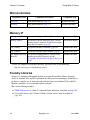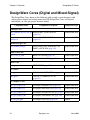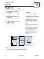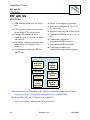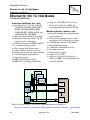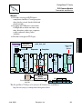
1
DesignWare® IP Family
Reference Guide
June 2009
DesignWare IP Family
Copyright Notice and Proprietary Information
Copyright © 2009 Synopsys, Inc. All rights reserved. This software and documentation contain confidential and
proprietary information that is the property of Synopsys, Inc. The software and documentation are furnished under a
license agreement and may be used or copied only in accordance with the terms of the license agreement. No part of
the software and documentation may be reproduced, transmitted, or translated, in any form or by any means,
electronic, mechanical, manual, optical, or otherwise, without prior written permission of Synopsys, Inc., or as
expressly provided by the license agreement.
Destination Control Statement
All technical data contained in this publication is subject to the export control laws of the United States of America.
Disclosure to nationals of other countries contrary to United States law is prohibited. It is the reader’s responsibility to
determine the applicable regulations and to comply with them.
Disclaimer
SYNOPSYS, INC., AND ITS LICENSORS MAKE NO WARRANTY OF ANY KIND, EXPRESS OR IMPLIED, WITH
REGARD TO THIS MATERIAL, INCLUDING, BUT NOT LIMITED TO, THE IMPLIED WARRANTIES OF
MERCHANTABILITY AND FITNESS FOR A PARTICULAR PURPOSE.
Registered Trademarks (®)
Synopsys, AMPS, Cadabra, CATS, CRITIC, CSim, Design Compiler, DesignPower, DesignWare, EPIC, Formality,
HSIM, HSPICE, iN-Phase, in-Sync, Leda, MAST, ModelTools, NanoSim, OpenVera, PathMill, Photolynx, Physical
Compiler, PrimeTime, SiVL, SNUG, SolvNet, System Compiler, TetraMAX, VCS, and Vera are registered trademarks
of Synopsys, Inc.
Trademarks (™)
Active Parasitics, AFGen, Apollo, Astro, Astro-Rail, Astro-Xtalk, Aurora, AvanTestchip, AvanWaves, BOA, BRT,
ChipPlanner, Circuit Analysis, Columbia, Columbia-CE, Comet 3D, Cosmos, CosmosEnterprise, CosmosLE,
CosmosScope, CosmosSE, Cyclelink, DC Expert, DC Professional, DC Ultra, Design Advisor, Design Analyzer,
Design Vision, DesignerHDL, DesignTime, Direct RTL, Direct Silicon Access, Discovery, Dynamic-Macromodeling,
Dynamic Model Switcher, EDAnavigator, Encore, Encore PQ, Evaccess, ExpressModel, Formal Model Checker,
FoundryModel, Frame Compiler, Galaxy, Gatran, HANEX, HDL Advisor, HDL Compiler, Hercules, Hercules-II,
Hierarchical Optimization Technology, High Performance Option, HotPlace, HSIMplus, HSPICE-Link, iN-Tandem,
Integrator, Interactive Waveform Viewer, i-Virtual Stepper, Jupiter, Jupiter-DP, JupiterXT, JupiterXT-ASIC, JVXtreme,
Liberty, Libra-Passport, Library Compiler, Libra-Visa, Magellan, Mars, Mars-Rail, Mars-Xtalk, Medici, Metacapture,
Milkyway, ModelSource, Module Compiler, Nova-ExploreRTL, Nova-Trans, Nova-VeriLint, Orion_ec, Parasitic View,
Passport, Planet, Planet-PL, Planet-RTL, Polaris, Power Compiler, PowerCODE, PowerGate, ProFPGA, ProGen,
Prospector, Raphael, Raphael-NES, Saturn, ScanBand, Schematic Compiler, Scirocco, Scirocco-i, Shadow Debugger,
Silicon Blueprint, Silicon Early Access, SinglePass-SoC, Smart Extraction, SmartLicense, Softwire, Source-Level
Design, Star-RCXT, Star-SimXT, Taurus, TimeSlice, TimeTracker, Timing Annotator, TopoPlace, TopoRoute,
Trace-On-Demand, True-Hspice, TSUPREM-4, TymeWare, VCS Express, VCSi, Verification Portal, VFormal, VHDL
Compiler, VHDL System Simulator, VirSim, and VMC are trademarks of Synopsys, Inc.
Service Marks (SM)
MAP-in, SVP Café, and TAP-in are service marks of Synopsys, Inc.
SystemC is a trademark of the Open SystemC Initiative and is used under license.
ARM and AMBA are registered trademarks of ARM Limited.
Saber is a registered trademark of SabreMark Limited Partnership and is used under license.
PCI Express is a trademark of PCI-SIG.
All other product or company names may be trademarks of their respective owners.
Synopsys, Inc.
700 E. Middlefield Road
Mountain View, CA 94043
www.synopsys.com
2
Synopsys, Inc.
June 2009
DesignWare IP Family
Contents
Contents
Preface . . . . . . . . . . . . . . . . . . . . . . . . . . . . . . . . . . . . . . . . . . . . . . . . . . . . . . . . . . . . . . 9
About This Manual . . . . . . . . . . . . . . . . . . . . . . . . . . . . . . . . . . . . . . . . . . . . . . . . . . . . . . . . 9
Manual Overview . . . . . . . . . . . . . . . . . . . . . . . . . . . . . . . . . . . . . . . . . . . . . . . . . . . . . . 9
Typographical and Symbol Conventions . . . . . . . . . . . . . . . . . . . . . . . . . . . . . . . . . . . 10
Synopsys Common Licensing (SCL) . . . . . . . . . . . . . . . . . . . . . . . . . . . . . . . . . . . . . . . . . 10
Getting Help . . . . . . . . . . . . . . . . . . . . . . . . . . . . . . . . . . . . . . . . . . . . . . . . . . . . . . . . . . . . 11
Additional Information . . . . . . . . . . . . . . . . . . . . . . . . . . . . . . . . . . . . . . . . . . . . . . . . . 11
Comments? . . . . . . . . . . . . . . . . . . . . . . . . . . . . . . . . . . . . . . . . . . . . . . . . . . . . . . . . . . . . . 11
Chapter 1
Overview . . . . . . . . . . . . . . . . . . . . . . . . . . . . . . . . . . . . . . . . . . . . . . . . . . . . . . . . . . . 13
DesignWare Library . . . . . . . . . . . . . . . . . . . . . . . . . . . . . . . . . . . . . . . . . . . . . . . . . . . . . .
Building Block IP . . . . . . . . . . . . . . . . . . . . . . . . . . . . . . . . . . . . . . . . . . . . . . . . . . . . .
DesignWare AMBA Family of Components . . . . . . . . . . . . . . . . . . . . . . . . . . . . . . . .
Star IP Microprocessor and DSP Cores . . . . . . . . . . . . . . . . . . . . . . . . . . . . . . . . . . . .
Microcontrollers . . . . . . . . . . . . . . . . . . . . . . . . . . . . . . . . . . . . . . . . . . . . . . . . . . . . . .
Memory IP . . . . . . . . . . . . . . . . . . . . . . . . . . . . . . . . . . . . . . . . . . . . . . . . . . . . . . . . . .
Foundry Libraries . . . . . . . . . . . . . . . . . . . . . . . . . . . . . . . . . . . . . . . . . . . . . . . . . . . . .
Verification IP for Bus and I/O Standards . . . . . . . . . . . . . . . . . . . . . . . . . . . . . . . . . .
Board Verification IP . . . . . . . . . . . . . . . . . . . . . . . . . . . . . . . . . . . . . . . . . . . . . . . . . .
VCS Verification Library . . . . . . . . . . . . . . . . . . . . . . . . . . . . . . . . . . . . . . . . . . . . . . . . . .
DesignWare Cores (Digital and Mixed-Signal) . . . . . . . . . . . . . . . . . . . . . . . . . . . . . . . . .
DesignWare Star IP . . . . . . . . . . . . . . . . . . . . . . . . . . . . . . . . . . . . . . . . . . . . . . . . . . . . . . .
14
15
16
17
18
18
18
19
20
20
22
24
Chapter 1
AMBA Bus Fabric and Peripheral IP . . . . . . . . . . . . . . . . . . . . . . . . . . . . . . . . . . . . 25
DW_ahb
Advanced High-Performance Bus . . . . . . . . . . . . . . . . . . . . . . . . . . . . . . . . . . . . . 27
DW_ahb_dmac
AHB Central Direct Memory Access (DMA) Controller . . . . . . . . . . . . . . . . . . . 29
DW_ahb_eh2h
Enhanced AHB to AHB Bridge . . . . . . . . . . . . . . . . . . . . . . . . . . . . . . . . . . . . . . . 30
DW_ahb_h2h
AHB to AHB Bridge . . . . . . . . . . . . . . . . . . . . . . . . . . . . . . . . . . . . . . . . . . . . . . . 32
DW_ahb_icm
AHB Multi-layer Interconnection Matrix . . . . . . . . . . . . . . . . . . . . . . . . . . . . . . . 34
DW_ahb_ictl
AHB Interrupt Controller . . . . . . . . . . . . . . . . . . . . . . . . . . . . . . . . . . . . . . . . . . . . 35
DW_apb
Advanced Peripheral Bus . . . . . . . . . . . . . . . . . . . . . . . . . . . . . . . . . . . . . . . . . . . . 36
June 2009
Synopsys, Inc.
3
Contents
DesignWare IP Family
DW_apb_gpio
APB General Purpose Programmable I/O . . . . . . . . . . . . . . . . . . . . . . . . . . . . . . . 37
DW_apb_i2c
APB I2C Interface . . . . . . . . . . . . . . . . . . . . . . . . . . . . . . . . . . . . . . . . . . . . . . . . . 38
DW_apb_i2s
APB I2S Bus . . . . . . . . . . . . . . . . . . . . . . . . . . . . . . . . . . . . . . . . . . . . . . . . . . . . . . 40
DW_apb_ictl
APB Interrupt Controller . . . . . . . . . . . . . . . . . . . . . . . . . . . . . . . . . . . . . . . . . . . . 41
DW_apb_rap
APB Remap and Pause . . . . . . . . . . . . . . . . . . . . . . . . . . . . . . . . . . . . . . . . . . . . . . 42
DW_apb_rtc
APB Real Time Clock . . . . . . . . . . . . . . . . . . . . . . . . . . . . . . . . . . . . . . . . . . . . . . 43
DW_apb_ssi
APB Synchronous Serial Interface . . . . . . . . . . . . . . . . . . . . . . . . . . . . . . . . . . . . . 44
DW_apb_timers
APB Programmable Timers . . . . . . . . . . . . . . . . . . . . . . . . . . . . . . . . . . . . . . . . . . 46
DW_apb_uart
APB Universal Asynchronous Receiver/Transmitter . . . . . . . . . . . . . . . . . . . . . . . 47
DW_apb_wdt
APB Watchdog Timer . . . . . . . . . . . . . . . . . . . . . . . . . . . . . . . . . . . . . . . . . . . . . . 49
DW_axi
Multiple Address, Multiple Data AXI Interconnect . . . . . . . . . . . . . . . . . . . . . . . . 50
DW_axi_gm
Generic Interface (GIF) to AMBA AXI Module . . . . . . . . . . . . . . . . . . . . . . . . . . 52
DW_axi_gs
AMBA AXI Slave to Generic Interface (GIF) . . . . . . . . . . . . . . . . . . . . . . . . . . . . 53
DW_axi_hmx
Connects AMBA AXI Slave to AHB Master . . . . . . . . . . . . . . . . . . . . . . . . . . . . . 54
DW_axi_rs
AMBA AXI Register Slice . . . . . . . . . . . . . . . . . . . . . . . . . . . . . . . . . . . . . . . . . . . 55
DW_axi_x2h
AXI to AHB Bridge . . . . . . . . . . . . . . . . . . . . . . . . . . . . . . . . . . . . . . . . . . . . . . . . 56
DW_axi_x2p
Connects AMBA AXI Slave to AHP Master . . . . . . . . . . . . . . . . . . . . . . . . . . . . . 57
DW_axi_x2x
Connects AMBA AXI Master to AXI Slave . . . . . . . . . . . . . . . . . . . . . . . . . . . . . 59
DesignWare AMBA QuickStart
Collection of example designs for AMBA subsystems . . . . . . . . . . . . . . . . . . . . . 61
Memory IP . . . . . . . . . . . . . . . . . . . . . . . . . . . . . . . . . . . . . . . . . . . . . . . . . . . . . . . . . . . . . 64
DW_memctl
Memory Controller . . . . . . . . . . . . . . . . . . . . . . . . . . . . . . . . . . . . . . . . . . . . . . . . . 65
DW_rambist
Memory Built-In Self Test . . . . . . . . . . . . . . . . . . . . . . . . . . . . . . . . . . . . . . . . . . . 67
Microprocessors/Microcontrollers . . . . . . . . . . . . . . . . . . . . . . . . . . . . . . . . . . . . . . . . . . . 69
DW_6811
4
Synopsys, Inc.
June 2009
DesignWare IP Family
Contents
6811 Microcontroller . . . . . . . . . . . . . . . . . . . . . . . . . . . . . . . . . . . . . . . . . . . . . . . 70
DW8051
8051 Microcontroller . . . . . . . . . . . . . . . . . . . . . . . . . . . . . . . . . . . . . . . . . . . . . . . 72
Chapter 2
DesignWare Library Verification IP . . . . . . . . . . . . . . . . . . . . . . . . . . . . . . . . . . . . . 74
Overview . . . . . . . . . . . . . . . . . . . . . . . . . . . . . . . . . . . . . . . . . . . . . . . . . . . . . . . . . . . . . . . 74
Verification Models . . . . . . . . . . . . . . . . . . . . . . . . . . . . . . . . . . . . . . . . . . . . . . . . . . . . . . . 75
DesignWare AMBA AHB Models
Master, Slave, Monitor, Bus Interconnect . . . . . . . . . . . . . . . . . . . . . . . . . . . . . . . 76
DesignWare AMBA APB Models
Master, Slave, Monitor . . . . . . . . . . . . . . . . . . . . . . . . . . . . . . . . . . . . . . . . . . . . . . 78
DesignWare VIP for AMBA 3 AXI
Master, Slave, Monitor, Interconnect . . . . . . . . . . . . . . . . . . . . . . . . . . . . . . . . . . . 79
Board Verification IP
Simulation models for Board Verification . . . . . . . . . . . . . . . . . . . . . . . . . . . . . . . 81
Ethernet (10, 100, 1G, 10G) Models
Transceiver and Monitor . . . . . . . . . . . . . . . . . . . . . . . . . . . . . . . . . . . . . . . . . . . . 82
Ethernet Models
RMII Transceiver and Hub . . . . . . . . . . . . . . . . . . . . . . . . . . . . . . . . . . . . . . . . . . . 83
2C Model
I
Transceiver . . . . . . . . . . . . . . . . . . . . . . . . . . . . . . . . . . . . . . . . . . . . . . . . . . . . . . . 84
Memory Models
Simulation models of memory devices . . . . . . . . . . . . . . . . . . . . . . . . . . . . . . . . . 85
Open Core Protocol (OCP) Models
Master, Slave, and Monitor . . . . . . . . . . . . . . . . . . . . . . . . . . . . . . . . . . . . . . . . . . 86
PCI Express Models
Transceiver and Monitor . . . . . . . . . . . . . . . . . . . . . . . . . . . . . . . . . . . . . . . . . . . . 88
PCI / PCI-X Bus Models
Master, Slave, and Monitor . . . . . . . . . . . . . . . . . . . . . . . . . . . . . . . . . . . . . . . . . . 90
Serial ATA Models
Device and Monitor . . . . . . . . . . . . . . . . . . . . . . . . . . . . . . . . . . . . . . . . . . . . . . . . 92
Serial Input/Output Interface Models
Tranceiver and Monitor . . . . . . . . . . . . . . . . . . . . . . . . . . . . . . . . . . . . . . . . . . . . . 94
USB On-The-Go Models
Host and Device . . . . . . . . . . . . . . . . . . . . . . . . . . . . . . . . . . . . . . . . . . . . . . . . . . . 95
DesignWare FlexModels . . . . . . . . . . . . . . . . . . . . . . . . . . . . . . . . . . . . . . . . . . . . . . . . . . 96
Listing of FlexModels . . . . . . . . . . . . . . . . . . . . . . . . . . . . . . . . . . . . . . . . . . . . . . . . . . 96
DesignWare SmartModels . . . . . . . . . . . . . . . . . . . . . . . . . . . . . . . . . . . . . . . . . . . . . . . . . 98
SmartModel Features . . . . . . . . . . . . . . . . . . . . . . . . . . . . . . . . . . . . . . . . . . . . . . . . . . 98
SmartModel Types . . . . . . . . . . . . . . . . . . . . . . . . . . . . . . . . . . . . . . . . . . . . . . . . . . . . 98
SmartModel Timing Definitions . . . . . . . . . . . . . . . . . . . . . . . . . . . . . . . . . . . . . . . . . . 99
Specific Model Information . . . . . . . . . . . . . . . . . . . . . . . . . . . . . . . . . . . . . . . . . . . . . 99
June 2009
Synopsys, Inc.
5
Contents
DesignWare IP Family
Chapter 3
DesignWare Foundry Libraries . . . . . . . . . . . . . . . . . . . . . . . . . . . . . . . . . . . . . . . . 100
TSMC Libraries . . . . . . . . . . . . . . . . . . . . . . . . . . . . . . . . . . . . . . . . . . . . . . . . . . . . . . . . 100
TSMC Memory Compilers for 90LP and 65LP . . . . . . . . . . . . . . . . . . . . . . . . . . . . . . . . 105
Chartered Libraries . . . . . . . . . . . . . . . . . . . . . . . . . . . . . . . . . . . . . . . . . . . . . . . . . . . . . . 106
Chapter 4
DesignWare Cores (Digital and Mixed-Signal IP) . . . . . . . . . . . . . . . . . . . . . . . . . 108
dwc_ethernet_mac10_100_universal
Ethernet MAC 10/100 Universal Core . . . . . . . . . . . . . . . . . . . . . . . . . . . . . . . . . 111
dwc_ether_mac10_100_1000_universal
Ethernet MAC 10/100/1000 Universal Core . . . . . . . . . . . . . . . . . . . . . . . . . . . . 113
dwc_ether_xgmac
XGMAC 10G Ethernet MAC . . . . . . . . . . . . . . . . . . . . . . . . . . . . . . . . . . . . . . . . 115
dwc_ethernet_pcs
Ethernet Extension Sub-layer . . . . . . . . . . . . . . . . . . . . . . . . . . . . . . . . . . . . . . . . 117
dwc_mobile_storage
Mobile Storage Host Controller . . . . . . . . . . . . . . . . . . . . . . . . . . . . . . . . . . . . . . 119
dwc_1394_av_link
Synthesizable IEEE 1394 AVLink DTCP . . . . . . . . . . . . . . . . . . . . . . . . . . . . . . 121
dwc_1394_cphy-native
Synthesizable IEEE 1394 Cable PHY . . . . . . . . . . . . . . . . . . . . . . . . . . . . . . . . . 123
DDR2/3-Lite SDRAM Complete Solution
DDR2/3-Lite SDRAM Complete Solution . . . . . . . . . . . . . . . . . . . . . . . . . . . . . 125
DDR2/DDR SDRAM PHY and Controller
DDR2/DDR SDRAM Complete Solution . . . . . . . . . . . . . . . . . . . . . . . . . . . . . . 127
dwc_jpeg
Synthesizable JPEG CODEC . . . . . . . . . . . . . . . . . . . . . . . . . . . . . . . . . . . . . . . . 129
dwc_pci
Universal PCI Controller . . . . . . . . . . . . . . . . . . . . . . . . . . . . . . . . . . . . . . . . . . . 131
dwc_pci-x
Synthesizable PCI-X Controller and Test Environment . . . . . . . . . . . . . . . . . . . . 133
PCIe-AHB Bridge
PCI Express to AMBA 2.0 AHB Bridge . . . . . . . . . . . . . . . . . . . . . . . . . . . . . . . 135
PCIe-AXI Bridge
PCI Express to AMBA 3 AXI Bridge . . . . . . . . . . . . . . . . . . . . . . . . . . . . . . . . . 136
dwc_pci_express_ep
PCI Express Endpoint Synthesizable Core . . . . . . . . . . . . . . . . . . . . . . . . . . . . . 138
dwc_pci_express_rc
PCI Express Root Port Synthesizable Core . . . . . . . . . . . . . . . . . . . . . . . . . . . . . 140
dwc_pci_express_sw
PCI Express Switch/Bridge Synthesizable Core . . . . . . . . . . . . . . . . . . . . . . . . . 142
dwc_pci_express_dm
PCI Express RC/EP Dual Mode Synthesizable Core . . . . . . . . . . . . . . . . . . . . . . 144
dwcore_pcie_phy
6
Synopsys, Inc.
June 2009
DesignWare IP Family
Contents
PCI Express PHY IP . . . . . . . . . . . . . . . . . . . . . . . . . . . . . . . . . . . . . . . . . . . . . . 146
dwc_sata_ahci
Serial ATA AHCI . . . . . . . . . . . . . . . . . . . . . . . . . . . . . . . . . . . . . . . . . . . . . . . . . 148
DWC_dsata
Serial ATA Device . . . . . . . . . . . . . . . . . . . . . . . . . . . . . . . . . . . . . . . . . . . . . . . . 150
. . . . . . . . . . . . . . . . . . . . . . . . . . . . . . . . . . . . . . . . . . . . . . . . . . . . . . . . . . . . . . . 150
dwc_sata_phy
Serial ATA PHY IP . . . . . . . . . . . . . . . . . . . . . . . . . . . . . . . . . . . . . . . . . . . . . . . . 152
dwc_usb_1_1_device
Synthesizable USB 1.1 Device Controller . . . . . . . . . . . . . . . . . . . . . . . . . . . . . . 154
dwc_usb_1_1_ohci_host
Synthesizable USB 1.1 OHCI Host Controller . . . . . . . . . . . . . . . . . . . . . . . . . . 156
dwc_usb_1_1_hub-native
Synthesizable USB 1.1 Hub Controller . . . . . . . . . . . . . . . . . . . . . . . . . . . . . . . . 158
dwc_usb_2_0_host_subsystem-pci-ahb
Synthesizable USB 2.0 Host Controller . . . . . . . . . . . . . . . . . . . . . . . . . . . . . . . . 160
dwc_usb_2_0_hs_otg_subsystem-ahb
Synthesizable Hi-Speed USB On-The-Go (OTG) Controller Subsystem . . . . . . 162
dwc_usb_2_0_device
Synthesizable USB 2.0 Device Controller . . . . . . . . . . . . . . . . . . . . . . . . . . . . . . 164
dwc_usb2_phy
USB 2.0 Transceiver Macrocell Interface PHY . . . . . . . . . . . . . . . . . . . . . . . . . . 166
dwc_usb2_hsotg_phy
USB 2.0 Hi-Speed OTG PHY . . . . . . . . . . . . . . . . . . . . . . . . . . . . . . . . . . . . . . . 168
dwc_wiusb_device_controller
Wireless USB Device Controller . . . . . . . . . . . . . . . . . . . . . . . . . . . . . . . . . . . . . 170
dwc_usb2_nanophy
USB 2.0 nanoPHY . . . . . . . . . . . . . . . . . . . . . . . . . . . . . . . . . . . . . . . . . . . . . . . . 172
dwc_xaui_phy
XAUI PHY IP . . . . . . . . . . . . . . . . . . . . . . . . . . . . . . . . . . . . . . . . . . . . . . . . . . . . 174
Chapter 5
DesignWare Star IP . . . . . . . . . . . . . . . . . . . . . . . . . . . . . . . . . . . . . . . . . . . . . . . . . 176
DW_IBM460-S, DW_IBM405-S
IBM PowerPC 460 and 405 CPU Cores . . . . . . . . . . . . . . . . . . . . . . . . . . . . . . . 177
DW_CoolFlux
CoolFlux 24-bit DSP Core from NXP . . . . . . . . . . . . . . . . . . . . . . . . . . . . . . . . . 179
DWC_n2p
Nios II Processor Core . . . . . . . . . . . . . . . . . . . . . . . . . . . . . . . . . . . . . . . . . . . . 182
Features . . . . . . . . . . . . . . . . . . . . . . . . . . . . . . . . . . . . . . . . . . . . . . . . . . . . . . . . . . . . 182
Index . . . . . . . . . . . . . . . . . . . . . . . . . . . . . . . . . . . . . . . . . . . . . . . . . . . . . . . . . . . . . . 184
June 2009
Synopsys, Inc.
7
Contents
8
DesignWare IP Family
Synopsys, Inc.
June 2009
DesignWare IP Family
Preface
Preface
About This Manual
This manual is a brief overview of the DesignWare Family of synthesizable and
verification IP. For detailed product information, refer to individual product databooks
and manuals mentioned in the following chapters.
Note
DesignWare Building Block component information has been moved from
this document to a separate document, the DesignWare Building Blocks
Quick Reference Guide.
Manual Overview
This manual contains the following chapters:
Preface
Describes the manual and typographical
conventions and symbols; tells how to get
technical assistance.
Chapter 1
“Overview”
Contains an overview and general description
of the DesignWare Library product offering.
Chapter 1
“AMBA Bus Fabric and Peripheral IP”
Describes the available DesignWare Library
AMBA/AXI Bus Fabric and Peripheral IP.
Chapter 2
“DesignWare Library Verification IP”
Describes the available DesignWare Library
verification models.
Chapter 3
“DesignWare Foundry Libraries”
This chapter briefly describes the
DesignWare Foundry Libraries.
June 2009
Synopsys, Inc.
9
Preface
DesignWare IP Family
Chapter 4
“DesignWare Cores (Digital and MixedSignal IP)”
Contains a brief description of each
DesignWare Core.
Chapter 5
“DesignWare Star IP”
Contains a brief description of each
DesignWare Star IP core.
Typographical and Symbol Conventions
Table 1 lists the conventions that are used throughout this document.
Table 1: Documentation Conventions
Convention
Description and Example
%
Represents the UNIX prompt.
Bold
User input (text entered by the user).
% cd $LMC_HOME/hdl
Monospace
System-generated text (prompts, messages, files, reports).
No Mismatches: 66 Vectors processed: 66 Possible"
Italic or Italic
Variables for which you supply a specific value. As a command
line example:
% setenv LMC_HOME prod_dir
In body text:
In the previous example, prod_dir is the directory where your
product must be installed.
| (Vertical rule)
Choice among alternatives, as in the following syntax example:
-effort_level low | medium | high
[ ] (Square brackets)
Enclose optional parameters:
pin1 [pin2 ... pinN]
In this example, you must enter at least one pin name (pin1), but
others are optional ([pin2 … pinN]).
TopMenu > SubMenu
Pulldown menu paths, such as:
File > Save As …
Synopsys Common Licensing (SCL)
You can find general Licensing (SCL) information on the Web at:
http://www.synopsys.com/Support/Licensing
10
Synopsys, Inc.
June 2009
DesignWare IP Family
Preface
Getting Help
If you have a question about using Synopsys products, please consult product documentation
that is installed on your network or located at the root level of your Synopsys product CD-ROM
(if available). You can also access documentation for DesignWare products on the Web:
●
Product documentation for many DesignWare products:
http://www.synopsys.com/dw/dwlibdocs.php
●
Datasheets for individual DesignWare IP components, located using “Search for IP”:
http://www.synopsys.com/designware
You can also contact the Synopsys Support Center in the following ways:
●
Open a call to your local support center by clicking this link and then accessing “Open a
Support Case.”
http://www.synopsys.com/Support
●
Support center contact information:
http://www.synopsys.com/Support/GlobalSupportCenters
Comments?
To report errors or make suggestions, please send e-mail to:
[email protected].
To report an error that occurs on a specific page, select the entire page (including headers and
footers), and copy to the buffer. Then paste the buffer to the body of your e-mail message. This
will provide us with information to identify the source of the problem.
June 2009
Synopsys, Inc.
11
Preface
12
DesignWare IP Family
Synopsys, Inc.
June 2009
DesignWare IP Family
Chapter 1: Overview
Overview
1
Overview
Synopsys DesignWare IP, the world’s most widely-used, silicon-proven IP provides
designers with a broad portfolio of synthesizable implementation IP, hardened PHYs
and verification IP for ASIC, SoC and FPGA designs. The DesignWare family includes
the following products:
●
“DesignWare Library” on page 14 - contains the principal ingredients for design and
verification including high speed datapath components, AMBA On-Chip Bus,
memory portfolio, verification models of standard bus and I/Os, foundry libraries,
popular Star IP cores and board verification IP.
●
“VCS Verification Library” on page 20 - is a subset of the DesignWare Library and
contains reusable, pre-verified verification IP of the industry's most popular bus and
interface standards such as AMBA, PCI Express, PCI-X, PCI, USB On-the-Go,
Ethernet, I2C and thousands of memory models.
●
“DesignWare Cores (Digital and Mixed-Signal)” on page 22 - silicon-proven,
digital and mixed-signal standards-based connectivity IP such as PCI Express,
PCI-X, PCI, USB 2.0 On-the-Go (OTG), USB 2.0 PHY, USB 1.1 and Ethernet.
●
“DesignWare Star IP” on page 24 - high-performance, high-value cores from
leading Star IP providers such as IBM, Infineon Technologies, MIPS Technologies,
NEC and Philips.
June 2009
Synopsys, Inc.
13
Chapter 1: Overview
DesignWare IP Family
DesignWare Library
The DesignWare Library provides designers with a comprehensive collection of
synthesizable IP, verification IP and foundry libraries. The library contains the following
principal ingredients for ASIC, SoC, and FPGA design and verification:
●
Building Block IP (Datapath, Data Integrity, DSP, Test, and more)
●
AMBA Bus Fabric, Peripherals, and Verification IP
●
Memory portfolio (memory controller, memory BIST, memory models and more)
●
Verification models of popular bus and I/O Standards (PCI Express, PCI-X, PCI,
USB On-the-Go, and more)
●
Microprocessor and DSP cores from industry-leading Star IP providers
●
Foundry Libraries
●
Board verification IP
●
Microcontrollers (8051 and 6811)
A single license gives you access to all the IP in the library. For more information on the
DesignWare Library, refer to the following:
http://www.synopsys.com/products/designware/dwlibrary.html
For a detailed search of the available IP, refer to the following:
http://www.synopsys.com/products/designware
14
Synopsys, Inc.
June 2009
DesignWare IP Family
Chapter 1: Overview
The DesignWare Building Block IP is a collection of over 200 technology-independent,
high-quality, high-performance IP. Most of these IP elements include multiple
implementations to provide a variety of performance and area tradeoff options.
Component groups for the Building Block IP are identified in the following table. For
more detail, refer to the DesignWare Building Blocks Quick Reference Guide.
Component Group
Description
Component Type
Low Power
New components, and enhanced DWBB components Synthesizable
that incorporate power-saving features, such as clock RTL
gating, piplining, and operand isolation.
NOTE: A special implementation and license (“lpwr”
/ DesignWare-LowPower) is required to enable these
new low power components and DWBB low power
enhancements.
Datapath
Arithmetic, floating point, trigonometric, and
sequential math IP
Synthesizable
RTL
Data Integrity
Data integrity IP such as CRC, ECC, 8b10b...
Synthesizable
RTL
Digital Signal
Processing (DSP)
FIR and IIR filters
Synthesizable
RTL
Application
Specific
Debugger IP
Synthesizable
RTL
Logic
Combinational, sequential, and control IP
Synthesizable
RTL
Interface
Clock Domain Crossing (CDC)
Synthesizable
RTL
Memory
Registers, FIFO, synchronous and asynchronous
RAM, and stack IP
Synthesizable
RTL
Test
JTAG IP such as boundary scan, TAP controller
Synthesizable
RTL
GTECH
Technology-independent IP library to aid users in Synthesizable
RTL
developing technology-independent parts
June 2009
Synopsys, Inc.
15
Overview
Building Block IP
Chapter 1: Overview
DesignWare IP Family
DesignWare AMBA Family of Components
AMBA is a standard bus architecture system developed by ARM for rapid development
of processor-driven systems. The AMBA standard also allows a number of bus
peripherals and resources to be connected in a consistent way. The following is a
complete listing of the Synopsys DesignWare IP for the AMBA protocol.
Component Name
DesignWare AMBA Synthesizable IP
DW_ahb
AHB bus, arbitration, decode, and control logic (page 27)
DW_ahb_dmac
AHB Central Direct Memory Access (DMA) Controller (page 29)
DW_ahb_h2h
AHB to AHB Bridge (page 32)
DW_ahb_eh2h
Enhanced AHB to AHB Bridge (page 30)
DW_ahb_icm
AHB Multi-layer Interconnection Matrix (page 34)
DW_ahb_ictl
AHB Interrupt Controller (page 35)
DW_apb
APB bus, decode, and bridge (page 36)
DW_apb_gpio
APB General Purpose I/O (GPIO) (page 37)
DW_apb_i2c
APB I2C Interface (page 38)
DW_apb_i2s
APB I2S Interface (page 40)
DW_apb_ictl
APB Interrupt Controller (page 41)
DW_apb_rap
APB Remap & Pause (page 42)
DW_apb_rtc
APB Real Time Clock (page 43)
DW_apb_ssi
APB Synchronous Serial Interface (page 44)
DW_apb_timers
APB Timer (page 46)
DW_apb_uart
APB UART (page 47)
DW_apb_wdt
APB Watch Dog Timer (page 49)
DW_memctl
Memory Controller (page 65)
DW_axi
Multiple Address, Multiple Data AXI Interconnect (page 50)
DW_axi_gm
Generic Interface (GIF) to AMBA AXI Module (page 52)
DW_axi_gs
AMBA AXI Slave to Generic Interface (page 53)
DW_axi_hmx
Connects AMBA AXI Slave to AHB Master (page 54)
16
Synopsys, Inc.
June 2009
DesignWare IP Family
Chapter 1: Overview
DesignWare AMBA Synthesizable IP
DW_axi_rs
AMBA AXI Register Slice (page 55)
DW_axi_x2h
AXI to AHB Bridge (page 56)
DW_axi_x2p
AXI to APB Bridge (page 57)
DW_axi_x2x
AXI to AXI Bridge (page 59)
Component Name
Overview
Component Name
DesignWare AMBA Component Description — Verification IP
ahb_bus_vmt
ahb_master_vmt
ahb_monitor_vmt
ahb_slave_vmt
AHB Bus Interconnect (page 76)
AHB Master (page 76)
AHB Monitor (page 76)
AHB Slave (page 76)
apb_master_vmt
apb_monitor_vmt
apb_slave_vmt
APB Master (page 78)
APB Monitor (page 78)
APB Slave (page 78)
axi_master_vmt
DesignWare VIP for AMBA 3 AXI (page 79)
axi_slave_vmt
axi_monitor_vmt
axi_interconnect_vmt
DesignWare AMBA QuickStart
The DesignWare AMBA QuickStart (page 61) is a collection of example designs for
AMBA subsystems built with DesignWare AMBA components. The QuickStart
example designs are static, non-reconfigurable examples of complete subsystems that
use DesignWare AMBA synthesizable IP and VIP components.
Star IP Microprocessor and DSP Cores
Component Name
Component Description
Component Type
DW_IBM460-S,
DW_IBM405-S
PowerPC 440 32-Bit Microprocessor Cores
from IBM (page 177)
Synthesizable RTLa
Verification Model
DW_CoolFlux
CoolFlux 24-bit DSP Core from Philips
(page 179)
Synthesizable RTLa
Verification Model
DWC_n2p
Nios II Processor Core (page 182)
Synthesizable RTLa
a. Verification models of these cores are included in the DesignWare Library and the DesignWare
Verification Library. Synthesizable RTL of these cores are available through the Star IP
Program. For more information visit: http://www.synopsys.com/designware/star_ip.html.
June 2009
Synopsys, Inc.
17
Chapter 1: Overview
DesignWare IP Family
Microcontrollers
Component Name
Component Description
Component Type
DW_6811
8-Bit Microcontroller (page 70)
Synthesizable RTL
DW8051
8-Bit Microcontroller (page 72)
Synthesizable RTL
Memory IP
Component Name
Component Description
Component Type
Memory Models
DesignWare contains thousands of pre-verified
memory models, with over 10,000 devices from
more than 25 vendors. (page 85)
Verification Models
DW_memctl
DesignWare Memory Controller (page 65)
Synthesizable RTL
DW_rambist
DesignWare Memory BIST solution (page 67)
Synthesizable RTL
DW Memory Building DesignWare Building Block IP contains many
Block IP
memory-related IP. For details, see the
Synthesizable RTL
DesignWare Building Blocks Quick Reference
Guide
To view the complete DesignWare memory portfolio, refer to the following:
http://www.synopsys.com/memorycentral
Foundry Libraries
Synopsys is teaming with foundry leaders to provide DesignWare Library licensees
access to standard cells and I/Os optimized for their process technologies. Each library
includes a complete set of front-end and back-end views for Standard Cells and I/Os.
Memory compilers are also included when available.
The current offering includes:
18
●
TSMC Libraries for 0.15um, 0.13um and 90nm and 65nm, described on page 100.
●
Chartered Libraries for 0.35um, 0.25um, 0.18um, and 0.13um, described on
page 106.
Synopsys, Inc.
June 2009
DesignWare IP Family
Chapter 1: Overview
Overview
Verification IP for Bus and I/O Standards
Component Name
Component Description
Type
ahb_bus_vmt,
ahb_master_vmt,
ahb_monitor_vmt,
ahb_slave_vmt
DesignWare VIP for AMBA 2.0 AHB Models
(page 76)
Verification
apb_master_vmt,
apb_monitor_vmt,
apb_slave_vmt
DesignWare VIP for AMBA 2.0 APB Models
(page 78)
Verification
axi_master_vmt,
axi_slave_vmt,
axi_monitor_vmt,
axi_interconnect_vmt
DesignWare VIP for AMBA 3 AXI (page 79)
Verification
ethernet_txrx_vmt,
ethernet_monitor_vmt
10/100/1G/10G Ethernet Models (page 82)
Verification
enethub_fx,
rmiirs_fx
Ethernet RMII Transceiver and Hub (page 83)
Verification
i2c_txrx_vmt
I2C Bi-Directional Two-Wire Bus (page 84)
Verification
pcie_txrx_vmt,
pcie_monitor_vmt
PCI Express 1.00a (page 88)
Verification
pcimaster_fx,
pcislave_fx,
pcimonitor_fx
PCI 2.3 and PCI-X 2.0 Simulation Models and Test
Suite (page 90)
Verification
sata_device_vmt,
sata_monitor_vmt
Serial ATA Models (page 92)
Verification
sio_txrx_vmt,
sio_monitor_vmt
Serial Input/Output Interface Models (page 94)
Verification
usb_host_vmt,
usb_device_vmt,
usb_monitor_vmt
USB On-The-Go Models, 1.1, 2.0, OTG, UTMI, and
UTMI+ Low Pin Interface (ULPI) (page 95)
Verification
June 2009
Synopsys, Inc.
19
Chapter 1: Overview
DesignWare IP Family
Board Verification IP
The DesignWare Library contains over 18,500 simulation models for ASIC, SoC, and
Board verification. For a complete search, visit http://www.synopsys.com/ipdirectory.
Component Group
Component Reference
VMT Models
Refer to “DesignWare Library Verification IP” on page 74
FlexModels
Refer to “DesignWare FlexModels” on page 96
DesignWare Memory Models Refer to “Memory Models” on page 85
SmartModel Library
Refer to “DesignWare SmartModels” on page 98
VCS Verification Library
The VCS Verification Library contains a broad portfolio of verification IP for the
industry's most popular bus protocols including AMBA 3 AXI, AMBA 2.0, PCI
Express, USB 2.0 OTG, Ethernet, Serial ATA and thousands of memory models. The
following table identifies the various components that make up this library.
Component Name
Component Description
Component Type
DesignWare Bus & I/O Standards
ahb_bus_vmt,
ahb_master_vmt,
ahb_monitor_vmt,
ahb_slave_vmt
DesignWare VIP for AMBA 2.0 AHB Models:
AHB Bus Interconnect, AHB Master, AHB
Monitor and AHB Slave (page 76)
Verification Models
apb_master_vmt,
apb_monitor_vmt,
apb_slave_vmt
DesignWare VIP for AMBA 2.0 APB Models:
APB Master, APB Monitor and APB Slave
(page 78)
Verification Models
axi_master_vmt
DesignWare VIP for AMBA 3 AXI (page 79)
axi_slave_vmt
axi_monitor_vmt
axi_interconnect_vmt
Verification Model
ethernet_txrx_vmt,
10/100/1G/10G Gigabit Ethernet Models (page 82) Verification Models
ethernet_monitor_vmt
enethub_fx, rmiirs_fx Ethernet RMII Transceiver and Hub (page 83)
Verification Models
i2c_txrx_vmt
Verification Model
20
I2C Bi-Directional Two-Wire Bus (page 84)
Synopsys, Inc.
June 2009
DesignWare IP Family
Chapter 1: Overview
PCI Express 1.00a (page 88)
Verification Model
pcimaster_fx,
pcislave_fx,
pcimonitor_fx
PCI/PCI-X Simulation Model and Test Suite
(page 90)
Verification Models
usb_host_vmt,
usb_device_vmt,
usb_monitor_vmt
USB On-The-Go Models, 1.1, 2.0, OTG, UTMI,
and UTMI+(page 95)
Verification Model
sio_txrxvmt,
sio_monitor_vmt
Serial Input/Output Interface Models (page 94)
Verification Models
DesignWare Design Views of Star IP Cores
DW_IBM460-S,
DW_IBM405-S
PowerPC 440 Microprocessor Cores from IBM
(page 177)
Verification Model
DW_CoolFlux
CoolFlux 24-bit DSP Core from Philips (page 179) Verification Model
DWC_n2p
Nios II Processor Core (page 182)
Synthesizable RTL
DesignWare Memory
Access to the full suite of memory IP is made available through DesignWare Memory Central; a
memory-focused Web site that lets designers download DesignWare Memory IP and
documentation. Visit Memory Central at:
http://www.synopsys.com/products/designware/memorycentral
Also visit the DesignWare Verification Library web page at:
http://www.synopsys.com/products/designware/dwverificationlibrary.html
June 2009
Synopsys, Inc.
21
Overview
pcie_txrx_vmt,
pcie_monitor_vmt
Chapter 1: Overview
DesignWare IP Family
DesignWare Cores (Digital and Mixed-Signal)
The DesignWare Cores shown in the following table provide system designers with
silicon-proven, digital and analog connectivity IP. DesignWare Cores are licensed
individually, on a fee-per-project business model.
Component Name
Component Description
Component Type
Ethernet Cores
dwc_ethernet_mac10_100_un Ethernet MAC 10/100 Universal
iversal
(page 111)
Synthesizable RTL
dwc_ether_mac10_100_1000 Ethernet MAC 10/100/1G Universal
_universal
(page 113)
Synthesizable RTL
Mobile Storage Core
dwc_mobile_storage
Secure Digital (SD), Multimedia Card
(MMC) and CE-ATA (page 119)
Synthesizable RTL
dwc_1394_av_link
IEEE 1394 AVLink (page 121)
Synthesizable RTL
dwc_1394_cphy-native
IEEE 1394 Cable PHY (page 123)
Synthesizable RTL
JPEG CODEC (page 129)
Synthesizable RTL
IEEE 1394 Cores
JPEG Core
dwc_jpeg
PCI Cores
dwc_pci
32/64 bit, 33/66-MHz PCI Core (page 131) Synthesizable RTL
dwc_pci-x
32/64 bit, 133-MHz PCI-X Core
(page 133)
Synthesizable RTL
dwc_pci_express_ep
PCI Express Endpoint Core (page 138)
Synthesizable RTL
dwc_pci_express_rc
PCI Express Root Port Core (page 140)
Synthesizable RTL
dwc_pci_express_sw
PCI Express Switch Port Core (page 142)
Synthesizable RTL
dwc_pci_express_dm
PCI Express Dual Mode Core (page 144)
Synthesizable RTL
dwcore_pcie_phy
PCI Express PHY Core (page 146)
Hard IP
PCI Express Cores
22
Synopsys, Inc.
June 2009
DesignWare IP Family
Chapter 1: Overview
dwc_sata_ahci
SATA Host (page 148)
Synthesizable RTL
DWC_dsata
SATA Host (page 150)
Synthesizable RTL
dwc_sata_phy
SATA PHY (page 152)
Hard IP
dwc_usb_1_1_device
USB 1.1. Device Controller (page 154)
Synthesizable RTL
dwc_usb_1_1_ohci_host
USB 1.1 OHCI Host Controller (page 156) Synthesizable RTL
dwc_usb_1_1_hub-native
USB 1.1. Hub Controller (page 158)
Synthesizable RTL
dwc_usb_2_0_host_subsyste
m-pci-ahb
USB 2.0 Host Controller - UHOST2
(page 160)
Synthesizable RTL
USB Cores
dwc_usb_2_0_hs_otg_subsyst USB 2.0 Hi-Speed On-the-Go Controller
em-ahb
Subsystem (page 162)
Synthesizable RTL
dwc_usb_2_0_device
USB 2.0 Device Controller (page 164)
Synthesizable RTL
dwc_usb2_phy
USB 2.0 PHY (page 166)
Hard IP
dwc_usb2_hsotg_phy
USB 2.0 Hi-Speed On-the-Go PHY
(page 168)
Hard IP
dwc_wiusb_device_controller Wireless USB Device Controller
(page 170)
Synthesizable RTL
dwc_usb2_nanophy
USB 2.0 nanoPHY (page 172)
Hard IP
XAUI PHY (page 174)
Hard IP
XAUI
dwc_xaui_phy
Also visit the DesignWare Cores web page at:
http://www.synopsys.com/products/designware/dwcores.html
June 2009
Synopsys, Inc.
23
Overview
SATA Cores
Chapter 1: Overview
DesignWare IP Family
DesignWare Star IP
Synopsys offers DesignWare Library users the ability to evaluate and design easily at
their desktop using the following high-performance, high-value IP cores from leading
Star IP providers.
Component Name
Component Description
Component Type
DW_IBM460-S,
DW_IBM405-S
PowerPC 440 Microprocessor Core from
IBM (page 177)
Synthesizable RTLa
Simulation Model
DW_CoolFlux
CoolFlux 24-bit DSP Core from NXP
(page 179)
Synthesizable RTLa
Simulation Model
DWC_n2p
Nios II Processor Core (page 182)
Synthesizable RTLa
Simulation Model
a. Simulation models of these cores are included in the DesignWare Library and DesignWare
Verification Library. Synthesizable RTL of these cores are available through the Star IP
Program.
Also visit the DesignWare Star IP web page at:
http://www.synopsys.com/products/designware/star_ip.html
24
Synopsys, Inc.
June 2009
DesignWare IP Family
AMBA Bus Fabric and Peripheral IP
AMBA is a standard bus architecture system developed by ARM for rapid development
of processor-driven systems. AMBA also allows a number of bus peripherals and
resources to be connected in a consistent way. The following Synopsys DesignWare
AMBA 2.0 and 3.0-compliant components are briefly described in this section:
Component Name
DesignWare AMBA Synthesizable IP
DW_ahb
AHB bus, arbitration, decode, and control logic (page 27)
DW_ahb_dmac
AHB Central Direct Memory Access (DMA) Controller (page 29)
DW_ahb_eh2h
Enhanced AHB to AHB Bridge (page 30)
DW_ahb_h2h
AHB to AHB Bridge (page 32)
DW_ahb_icm
AHB Multi-layer Interconnection Matrix (page 34)
DW_ahb_ictl
AHB Interrupt Controller (page 35)
DW_apb
APB bus, decode, and bridge (page 36)
DW_apb_gpio
APB General Purpose I/O (GPIO) (page 37)
DW_apb_i2c
APB I2C Interface (page 38)
DW_apb_i2s
APB I2S Interface (page 40)
DW_apb_ictl
APB Interrupt Controller (page 41)
DW_apb_rap
APB Remap & Pause (page 42)
DW_apb_rtc
APB Real Time Clock (page 43)
DW_apb_ssi
APB Synchronous Serial Interface (page 44)
DW_apb_timers
APB Timer (page 46)
June 2009
Synopsys, Inc.
25
DWL Sythesizable IP
1
DesignWare IP Family
Component Name
DesignWare AMBA Synthesizable IP
DW_apb_uart
APB UART (page 47)
DW_apb_wdt
APB Watch Dog Timer (page 49)
DW_memctl
Memory Controller (page 65)
DW_axi
Multiple Address, Multiple Data AXI Interconnect (page 50)
DW_axi_gm
Generic Interface (GIF) to AMBA AXI Module (page 52)
DW_axi_gs
AMBA AXI Slave to Generic Interface (page 53)
DW_axi_hmx
AMBA AXI Slave to AHB Master Interface (page 54)
DW_axi_rs
AMBA AXI Register Slice (page 55)
DW_axi_x2h
AXI to AHB Bridge (page 56)
DW_axi_x2p
AXI to APB Bridge (page 57)
DW_axi_x2x
AXI Master to AXI Slave Bridge (page 59)
A brief introduction to DesignWare AMBA components is available at the following
location:
http://www.synopsys.com/products/designware/dw_amba.html
Source Licenses Available
You can configure any of the DesignWare AMBA synthesizable components and write
out encrypted RTL using only a DesignWare license. If you want to write unencrypted
RTL source code, you must purchase a special source license. For more information
about licenses, please refer to the DesignWare AMBA Synthesizable Components
Installation Guide:
www.synopsys.com/products/designware/docs/doc/amba/latest/dw_amba_install.pdf
DesignWare AMBA QuickStart
The DesignWare AMBA QuickStart (page 61) is a collection of example designs for
AMBA subsystems built with DesignWare AMBA synthesizable components. The
QuickStart example designs are static, non-reconfigurable examples of complete
subsystems that use DesignWare AMBA synthesizable and verification components.
26
Synopsys, Inc.
June 2009
DesignWare IP Family
A
C o M BA
mp
lian
t
DW_ahb
Advanced High-Performance Bus
DW_ahb
Advanced High-Performance Bus
●
●
●
●
●
●
●
●
●
●
●
●
●
Configuration of AMBA Lite system
Configuration of up to 15 masters in a
non-AMBA Lite system
Configuration of up to 15 slaves
Configuration of data bus width of up
to 256 bits
System address width of 32 or 64 bits
Configuration of system endianness —
big or little endian; can be controlled
by external input or set during
configuration of component
Optional arbiter slave interface
Optional internal decoder
Programmable arbitration scheme:
Weighted token
Programmable or fixed priority
Fair-Among-Equals
Arbitration for up to 15 masters
Individual grant signals for each
master
●
●
●
●
●
●
●
●
●
Support for split, burst, and locked
transfers
Optional support for early burst
termination
Configurable support for termination
of undefined length bursts by masters
of equal or higher priority
Configurable or programmable priority
assignments to masters
Disabling of masters and protection
against self disable
Optional support for AMBA memory
remap feature
Optional support for pausing of the
system, immediately or when bus is
IDLE
Contiguous and non-contiguous
memory allocation options for slaves
External debug mode signals, giving
visibility
Also, see the block diagram on the following page.
This component is coreAssembler ready. For more information about coreAssembler:
http://www.synopsys.com/products/designware/core_assembler.html
June 2009
Synopsys, Inc.
27
DWL Sythesizable IP
●
A
C o MB
mp A
lian
t
DesignWare IP Family
DW_ahb
Advanced High-Performance Bus
DW_ahb
Parameterizable
Master Signals
Arbiter
Slave 1
Master 1
Master 2
Slave 2
Address and
control MUX
.
.
.
Parameterizable
Slave Signals
.
.
.
Write data MUX
Master i
Slave j
Read data MUX
i = up to 15
j = up to 15
Decoder
(internal)
The DesignWare DW_ahb Databook is available at:
http://www.synopsys.com/products/designware/docs
28
Synopsys, Inc.
June 2009
DesignWare IP Family
A
C o M BA
mp
lian
t
DW_ahb_dmac
AHB Central Direct Memory Access (DMA) Controller
DW_ahb_dmac
AHB Central Direct Memory Access (DMA) Controller
●
●
●
AHB slave interface – used to program
the DW_ahb_dmac
AHB master interface(s)
❍ Up to four independent AHB
master interfaces that allows:
• Up to four simultaneous DMA
transfers
• Masters that can be on
different AMBA layers
(multi-layer support)
• Source and destination that
can be on different AMBA
layers (pseudo fly-by
performance)
❍ Configurable data bus width (up to
256 bits) for each AHB master
interface
❍ Configurable endianness for
master interfaces
Configurable identification register
Encoded parameters
●
●
●
●
Channels
❍ Up to eight channels, one per
source and destination pair
❍ Unidirectional channels – data
transfers in one direction only
❍ Programmable channel priority
Transfers
❍ Support for memory-to-memory,
memory-to-peripheral,
peripheral-to-memory, and
peripheral-to-peripheral DMA
transfers
❍ DW_ahb_dmac to or from APB
peripherals through the APB
bridge
Component parameters for
configurable software driver support
coreAssembler ready.
DW_ahb_dmac
Channel n
DMA Hardware
Request I/F
Arbiter
Master I/F
FIFO
Channel 0
AHB Slave I/F
The DesignWare DW_ahb_dmac Databook is available at:
http://www.synopsys.com/products/designware/docs
June 2009
Synopsys, Inc.
29
DWL Sythesizable IP
●
A
C o MB
mp A
lian
t
DesignWare IP Family
DW_ahb_eh2h
Enhanced AHB to AHB Bridge
DW_ahb_eh2h
Enhanced AHB to AHB Bridge
Clocks
●
●
●
AHB Master interface
Asynchronous or synchronous clocks,
any clock ratio
Fully registered outputs
Optional pipeline stages to reduce
logic levels on bus inputs
AHB Slave interface
●
●
●
●
●
●
●
●
●
●
●
●
●
●
●
●
●
Data width: 32,64,128, or 256 bits
Address width: 32 or 64 bits
Big or little endian
Lock and bus request generation
SINGLE, INCR burst type generation
for writes
Any burst type generation for reads
Downsizing of wider transfers
●
Data width: 32,64,128, or 256 bits
Address width: 32 or 64 bits
Write operations
Big or little endian
Zero or two wait states OKAY
● Configurable depth write buffer
response
● Buffered writes (always, HPROT is
don't care)
ERROR response
No RETRY response
● SPLIT response on write buffer full
SPLIT response
● Maximum of two wait states on
non-sequential access
HSPLIT generation
Handling of multiple, outstanding split
● Zero wait states (full bandwidth) on
transactions
sequential access
Multiple HSELs
● Zero BUSY cycles (full bandwidth),
secondary burst generation
HREADY low (alternative to SPLIT
response) operation mode
Read operations
Software interface
●
●
●
Interrupt signal on write errors
Interrupt status/clear registers
●
●
●
Sideband signals
●
●
30
Input sstall pin to qualify an address
phase for HREADY low operation
mode
Output sflush pin to monitor the
flushing operation on the read buffer
●
Synopsys, Inc.
Configurable depth read buffer
Pre-fetched reads
Non-prefetched reads
SPLIT response on non-sequential
(non yet prefetched) access
Zero wait states (full bandwidth) on
prefetched read data
June 2009
DesignWare IP Family
A
C o M BA
mp
lian
t
DW_ahb_eh2h
Enhanced AHB to AHB Bridge
Write Buffer
Bridge
Slave
Bridge
Master
^
^
Secondary
AHB
Read Buffer
sHCLK
mHCLK
This component is coreAssembler ready. For more information about coreAssembler:
http://www.synopsys.com/products/designware/core_assembler.html
The DesignWare DW_ahb_eh2h Databook is available at:
http://www.synopsys.com/products/designware/docs
June 2009
Synopsys, Inc.
31
DWL Sythesizable IP
Primary
AHB
A
C o MB
mp A
lian
t
DesignWare IP Family
DW_ahb_h2h
AHB to AHB Bridge
DW_ahb_h2h
AHB to AHB Bridge
System Level
●
●
●
●
●
AHB Slave Interface
Configurable asynchronous or
synchronous clocks – any clock ratio
Four clocking modes for synchronous
clock configurations – two with and
two without clock enables
Low-gate count implementation
(minimum configuration below 2K
gates)
Sub-optimal throughput performance
(non-buffered architecture)
High clock-speed operations (fully
registered outputs, operating
frequency more than 300 MHz)
●
●
●
●
●
●
●
●
●
●
32
●
●
●
●
●
AHB Master Interface
●
●
Deadlock protection: SPLIT response
generation after deadlock detection at
the master interface
Bus held off (HREADY low) until the
secondary transfer data phase
completes and is acknowledged back
from the master interface
SPLIT response (from secondary)
forwarded back to primary as RETRY
Component ID code retrievable from
read data bus
Support for locked transfers (any
HTRANS) through HMASTLOCK
IDLE and BUSY non-locked cycles
ignored
Configurable AHB address width (32
or 64 bits)
Configurable AHB data width (32, 64,
128, or 256 bits)
Configurable endianness
HLOCK generation
HBUSREQ generation
HTRANS: generation of IDLE or
NSEQ bus cycles
Non-pipelined transfers: address phase
always followed by IDLE cycles until
data phase completes
HBURST: fixed to SINGLE
All other AHB control signals
forwarded unchanged
AHB Lite configuration to remove
redundant logic
Deadlock detection
Synopsys, Inc.
June 2009
DesignWare IP Family
A
C o M BA
mp
lian
t
DW_ahb_h2h
AHB to AHB Bridge
core
sBIU
mBIU
DWL Sythesizable IP
REQ
sFSM
ACK
mFSM
sync
clock domain
boundary
This component is coreAssembler ready. For more information about coreAssembler:
http://www.synopsys.com/products/designware/core_assembler.html
The DesignWare DW_ahb_h2h Databook is available at:
http://www.synopsys.com/products/designware/docs
June 2009
Synopsys, Inc.
33
A
C o MB
mp A
lian
t
DesignWare IP Family
DW_ahb_icm
AHB Multi-layer Interconnection Matrix
DW_ahb_icm
AHB Multi-layer Interconnection Matrix
●
●
●
●
●
●
Layer arbitration and master
multiplexing
Input stage address and control
holding registers for each layer
Mapping of slave response onto
correct layer
Returning of splits onto the correct
layer
Common clock and reset shared
amongst all layers
coreAssembler ready.
●
User-defined parameters:
❍ AMBA Lite
❍ AHB address bus width, (same
width on all layers)
❍ AHB data bus width, (same width
on each layer)
❍ AHB master layers, (up to 4)
❍ Split or non-split capable slave
❍ Slave with/without multiple select
lines
❍ Slave with/without protection
control
❍ Slave with/without burst control
❍ Slave with/without lock control
❍ Layer release scheme
❍ Baseline arbitration scheme
❍ External arbitration priority
control
DW_ahb
Layer 1
.
.
.
DW_ahb_icm
DW_ahb
Slave
DW_ahb
Layer N
The DesignWare DW_ahb_icm Databook is available at:
http://www.synopsys.com/products/designware/docs
34
Synopsys, Inc.
June 2009
DesignWare IP Family
A
C o M BA
mp
lian
t
DW_ahb_ictl
AHB Interrupt Controller
DW_ahb_ictl
AHB Interrupt Controller
●
●
●
●
2 to 64 IRQ normal interrupt sources
1 to 8 FIQ fast interrupt sources
(optional)
Vectored interrupts (optional)
Software interrupts
Configuration ID registers
●
●
●
●
●
●
Priority filtering (optional)
Masking
Scan mode (optional)
Programmable interrupt priorities
(after configuration)
Encoded parameters
Note: Does not support split transfers
DW_ahb_ictl
IRQ
Generation
Interrupt
Registers
FIQ
Generation
Vector
Generation
&
Masking
This component is coreAssembler ready. For more information about coreAssembler:
http://www.synopsys.com/products/designware/core_assembler.html
The DesignWare DW_ahb_ictl Databook is available at:
http://www.synopsys.com/products/designware/docs
June 2009
Synopsys, Inc.
35
DWL Sythesizable IP
●
A
C o MB
mp A
lian
t
DesignWare IP Family
DW_apb
Advanced Peripheral Bus
DW_apb
Advanced Peripheral Bus
●
●
●
●
●
APB Bridge and APB bus functionality
incorporated
AHB slave
Supports up to 16 APB slaves
Supports big- and little-endian AHB
systems
Supports little-endian APB slaves
●
●
●
●
●
Supports 32, 64, 128, 256 AHB data
buses
Supports 8, 16, and 32-bit APB data
buses
Supports single and burst AHB
transfers
Supports synchronous hclk/pclk; hclk
is an integer multiple of pclk
The AHB slave side does not support
SPLIT, RETRY or ERROR responses
Configurable
Slave Signals (up to 16)
DW_apb
AHB
AHB Slave
Interface
Address
Decoder
Read Data
MUX
.
.
.
.
.
.
.
Slave 0
Slave j
j = up to 15
This component is coreAssembler ready. For more information about coreAssembler:
http://www.synopsys.com/products/designware/core_assembler.html
The DesignWare DW_apb Databook is available at:
http://www.synopsys.com/products/designware/docs
36
Synopsys, Inc.
June 2009
DesignWare IP Family
A
C o M BA
mp
lian
t
DW_apb_gpio
APB General Purpose Programmable I/O
DW_apb_gpio
APB General Purpose Programmable I/O
●
●
●
●
Up to 128 independently configurable
pins (If more than 128 pins are
required, another DW_apb_gpio
should be instantiated.)
Up to four ports, A to D, which are
separately configurable
Separate data registers and data
direction registers for each port
Configurable hardware and software
control for each port, or for each bit of
each port.
Separate auxiliary data input, data
output, and data control for each I/O in
Hardware Control mode
●
●
●
●
●
●
●
Independently controllable port bits
Configurable interrupt mode for Port
A
Configurable debounce logic with an
external slow clock to debounce
interrupts
Option to generate single or multiple
interrupts
GPIO Component Type register
GPIO Component Version register
Configurable reset values on output
ports
DW_apb_gpio
External Data
xpins
Port
I/O
Interface
APB
APB
Interface
AuxData
Interrupt
Detection
Interrupts
This component is coreAssembler ready. For more information about coreAssembler:
http://www.synopsys.com/products/designware/core_assembler.html
The DesignWare DW_apb_gpio Databook is available at:
http://www.synopsys.com/products/designware/docs
June 2009
Synopsys, Inc.
37
DWL Sythesizable IP
●
A
C o MB
mp A
lian
t
DesignWare IP Family
DW_apb_i2c
APB I2C Interface
DW_apb_i2c
APB I2C Interface
●
●
●
●
●
●
●
●
●
Two-wire I2C serial interface
Three speeds:
❍ Standard mode (100 Kb/s)
❍ Fast mode (400 Kb/s)
❍ High-speed mode (3.4 Mb/s)
Ignores CBUS addresses (an older
ancestor of I2C that used to share the
I2C bus)
Transmit and receive buffers
Interrupt or polled mode operation
Handles Bit and Byte waiting at all bus
speeds
Simple software interface consistent
with DesignWare APB peripherals
Digital filter for the received SDA and
SCL lines
Support for APB data bus widths of 8,
16, and 32 bits
DMA handshaking interface
compatible with the DW_ahb_dmac
handshaking interface
●
●
●
●
Supports clock synchronization
Master or slave I2C operation
Supports multi-Master operation (bus
arbitration)
7- or 10-bit addressing
7- or 10-bit combined format transfers
Slave bulk transfer mode
Component parameters for
configurable software driver support
●
●
●
●
DW_apb_i2c
APB Slave
Interface
I2C
Master/
Slave
DMA
Controller
Interface
TX-FIFO
Interrupts
RX-FIFO
RX Filter
Clock
Generator
38
I2C
Debug
Synopsys, Inc.
June 2009
DesignWare IP Family
A
C o M BA
mp
lian
t
DW_apb_i2c
APB I2C Interface
This component is coreAssembler ready. For more information about coreAssembler:
http://www.synopsys.com/products/designware/core_assembler.html
DWL Sythesizable IP
The DesignWare DW_apb_i2c Databook is available at:
http://www.synopsys.com/products/designware/docs
June 2009
Synopsys, Inc.
39
A
C o MB
mp A
lian
t
DesignWare IP Family
DW_apb_i2s
APB I2S Bus
DW_apb_i2s
APB I2S Bus
●
●
●
●
●
APB data bus widths of 8, 16, and 32
bits
Master or slave mode of operation
Audio data resolutions of 12, 16, 20,
24, and 32 bits
External sclk gating and enable signals
Configurable FIFO depth of 2, 4, 8, 16
bits
Configurable support for
programmable DMA registers
Programmable FIFO thresholds
Component parameters for
configurable software driver support
●
●
I2 S
transmitter and/or receiver based
on the Philips I2S serial protocol
Configurable number of stereo
channels (up to 4) for both transmitter
and receiver
Full duplex communication due to the
independence of transmitter and
receiver
Asynchronous clocking of APB bus
and I2S sclk
●
●
●
●
●
DW_apb_i2s
APB Slave
Interface
I2S
Register
Block
TX FIFOs
RX FIFOs
I2S
Transmitter
Block
I2S
Clock
Generation
I2S
Receiver
Block
This component is coreAssembler ready. For more information about coreAssembler:
http://www.synopsys.com/products/designware/core_assembler.html
The DesignWare DW_apb_i2s Databook is available at:
http://www.synopsys.com/products/designware/docs
40
Synopsys, Inc.
June 2009
DesignWare IP Family
A
C o M BA
mp
lian
t
DW_apb_ictl
APB Interrupt Controller
DW_apb_ictl
APB Interrupt Controller
●
●
●
2 to 64 IRQ normal interrupt sources
1 to 8 FIQ fast interrupt sources
(optional)
Vectored interrupts (optional)
Software interrupts
●
●
●
●
Priority filtering (optional)
Masking
Scan mode (optional)
Programmable interrupt priorities
(after configuration)
DWL Sythesizable IP
●
Note
DW_apb_ictl is an exact replacement for the original component
DW_amba_ictl (name change only).
DW_apb_ictl
IRQ
Generation
Interrupt
Registers
FIQ
Generation
Vector
Generation
&
Masking
This component is coreAssembler ready. For more information about coreAssembler:
http://www.synopsys.com/products/designware/core_assembler.html
The DesignWare DW_apb_ictl Databook is available at:
http://www.synopsys.com/products/designware/docs
June 2009
Synopsys, Inc.
41
A
C o MB
mp A
lian
t
DesignWare IP Family
DW_apb_rap
APB Remap and Pause
DW_apb_rap
APB Remap and Pause
●
●
●
Configuration of APB data bus width
8, 16, or 32
Remap Control: Used to switch the
DW_ahb address decoder from boot
mode to normal mode operation.
Pause Mode: Used to put the
DW_ahb's arbiter into low-power
(pause) mode.
In pause mode the dummy master is
granted the AHB bus until an interrupt
occurs.
Reset Status Register: Keeps track of
status from up to eight separate system
reset signals.
Identification Code Register:
Implements a configurable, read-only
ID register
●
●
●
DW_apb_rap
Registers
Remap
Pause
ID
APB
Interface
Reset
This component is coreAssembler ready. For more information about coreAssembler:
http://www.synopsys.com/products/designware/core_assembler.html
The DesignWare DW_apb_rap Databook is available at:
http://www.synopsys.com/products/designware/docs
42
Synopsys, Inc.
June 2009
DesignWare IP Family
A
C o M BA
mp
lian
t
DW_apb_rtc
APB Real Time Clock
DW_apb_rtc
APB Real Time Clock
●
●
●
APB slave interface with read/write
coherency for registers
Incrementing counter and comparator
for interrupt generation
Free-running pclk
User-defined parameters:
❍ APB data bus width
❍ Counter width
❍ Clock relationship between bus
clock and counter clock
❍ Interrupt polarity level
❍ Interrupt clock domain location
❍ Counter enable mode
❍ Counter wrap mode
●
Some uses of the DW_apb_rtc are:
❍ Real-time clock – used with
software for keeping track of time
❍ Long-term, exact chronometer –
When clocked with a 1 Hz clock,
it can keep track of time from now
up to 136 years in the future
❍ Alarm function – generates an
interrupt after a programmed
number of cycles
❍ Long-time, base counter – clocked
with a very slow clock signal
DW_apb_rtc
Counter
APB
Interface
Synchronization
Register
Block
Interrupt Generation
Up Counter
Read/Write
Coherency
This component is coreAssembler ready. For more information about coreAssembler:
http://www.synopsys.com/products/designware/core_assembler.html
The DesignWare DW_apb_rtc Databook is available at:
http://www.synopsys.com/products/designware/docs
June 2009
Synopsys, Inc.
43
DWL Sythesizable IP
●
A
C o MB
mp A
lian
t
DesignWare IP Family
DW_apb_ssi
APB Synchronous Serial Interface
DW_apb_ssi
APB Synchronous Serial Interface
●
●
●
●
●
●
●
44
AMBA APB interface – Allows for
easy integration into an AMBA
System on Chip (SoC)
implementation.
Scalable APB data bus width –
Supports APB data bus widths of 8,
16, and 32 bits.
Serial-master or serial-slave operation
– Enables serial communication with
serial-master or serial-slave peripheral
devices.
DMA Controller Interface – Enables
the DW_apb_ssi to interface to a
DMA controller over the AMBA bus
using a handshaking interface for
transfer requests.
Independent masking of interrupts –
Master collision, transmit FIFO
overflow, transmit FIFO empty,
receive FIFO full, receive FIFO
underflow, and receive FIFO overflow
interrupts can all be masked
independently.
Multi-master contention detection –
Informs the processor of multiple
serial-master accesses on the serial
bus.
Bypass of meta-stability flip-flops for
synchronous clocks – When the APB
clock (pclk) and the DW_apb_ssi
serial clock (ssi_clk) are synchronous,
meta-stable flip-flops are not used
when transferring control signals
across these clock domains.
●
●
Synopsys, Inc.
Programmable features:
❍ Serial interface operation – Choice
of Motorola SPI, Texas
Instruments Synchronous Serial
Protocol or National
Semiconductor Microwire.
❍ Clock bit-rate – Dynamic control
of serial bit rate of data transfer;
used in only serial-master mode.
❍ Data Item size (4 to 16 bits) – Item
size of each data transfer under
control of programmer.
Configurable features:
❍ FIFO depth – Configurable depth
of transmit and receive FIFO
buffers from 2 to 256 words deep;
FIFO width fixed at 16 bits.
❍ Number of slave select outputs –
When operating as serial master,
1 to 16 serial slave-select output
signals can be generated.
❍ Hardware/software slave-select –
Dedicated hardware slave-select
lines or software control for
targeting serial-slave device.
❍ Combined or individual interrupt
lines
❍ Interrupt polarity – Selects
serial-clock phase of SPI format
directly after reset.
June 2009
DesignWare IP Family
A
C o M BA
mp
lian
t
DW_apb_ssi
APB Synchronous Serial Interface
DW_apb_ssi
DWL Sythesizable IP
APB
Interface
Transmit
FIFO
Control
Shift
Control
Logic
Receive
FIFO
Control
Register
Block
Transmit
FIFO
Memory
Interrupt
Logic
DMA
Interface
Receive
FIFO
Memory
Clock
Pre-scale
FSM
Control
This component is coreAssembler ready. For more information about coreAssembler:
http://www.synopsys.com/products/designware/core_assembler.html
The DesignWare DW_apb_ssi Databook is available at:
http://www.synopsys.com/products/designware/docs
June 2009
Synopsys, Inc.
45
A
C o MB
mp A
lian
t
DesignWare IP Family
DW_apb_timers
APB Programmable Timers
DW_apb_timers
APB Programmable Timers
●
●
●
●
●
Up to eight programmable timers
Configurable timer width: 8 to 32 bits
Support for two operation modes:
free-running and user-defined count
Support for independent clocking of
timers
Configurable polarity for each
individual interrupt
●
●
●
Configurable option for a single or
combined interrupt output flag
Configurable option to have read/write
coherency registers for each timer
Configurable option to include timer
toggle output, which toggles each time
counter reloads
DW_apb_timers
Timer1
Timer2
TimerN*
* N <= 8
This component is coreAssembler ready. For more information about coreAssembler:
http://www.synopsys.com/products/designware/core_assembler.html
The DesignWare DW_apb_timers Databook is available at:
http://www.synopsys.com/products/designware/docs
46
Synopsys, Inc.
June 2009
A
C o M BA
mp
lian
t
DesignWare IP Family
DW_apb_uart
APB Universal Asynchronous Receiver/Transmitter
DW_apb_uart
APB Universal Asynchronous Receiver/Transmitter
●
●
●
●
●
●
●
●
AMBA APB interface allows easy
integration into AMBA SoC
implementations
Configurable APB data bus widths of
8, 16 and 32
Functionality based on the 16550
industry standard, that is as follows:
❍ Programmable character
properties, such as number of data
bits per character (5-8), optional
parity bit (with odd or even select)
and number of stop bits (1, 1.5 or
2)
❍ Line break generation and
detection
❍ DMA signaling with two
programmable modes
❍ Prioritized interrupt identification
Configurable selection of additional
DMA interface signals for
compatibility with DesignWare DMA
interface
Configurable selection of DMA
interface signal polarity
Configurable transmit and receive
FIFO depths of none, 16, 32,
64,…,2048
Configurable internal or external FIFO
(RAM) selection
Programmable FIFO enable/
disableExternal read enable signal for
RAM wake-up when using external
RAMs
Configurable selection of the use two
clocks (pclk and sclk) instead of one
(pclk)
●
●
●
●
●
●
●
●
●
●
Programmable Auto Flow Control
mode as specified in the 16750
standard
Programmable Transmitter Holding
Register Empty (THRE) interrupt
mode
Configurable IrDA 1.0 SIR mode
support with up to 115.2 Kbaud data
rate and a pulse duration (width) as
follows: width = 3/16 × bit period as
specified in the IrDA physical layer
specification
Programmable serial data baud rate
Configurable baud clock reference
output signal
Modem and status lines are
independently controlled
Programmable Loopback mode that
enables greater testing of Modem
Control and Auto Flow Control
features (Loopback support in IrDA
SIR mode is available)
Selectable clock gate enable output(s)
used to indicate that the TX and RX
pipeline is clear (no data) and no
activity has occurred for more than
one character time, so clocks may be
gated
Separate system resets for each clock
domain to prevent metastability
Selectable FIFO access mode (for
FIFO testing) so that the receive FIFO
can be written by the master and the
transmit FIFO can be read by the
master
Also see the block diagram on the following page.
June 2009
Synopsys, Inc.
47
DWL Sythesizable IP
●
A
C o MB
mp A
lian
t
DesignWare IP Family
DW_apb_uart
APB Universal Asynchronous Receiver/Transmitter
.
DW_apb_uart
FIFO
Block
(Optional)
APB
Interface
Register
Block
Reset
Block
Modem
Sync
Block
Sync
Block
(Optional)
Timeout
Detector
(Optional)
Baud
Clock
Generator
Serial Receiver
Serial Transmitter
This component is coreAssembler ready. For more information about coreAssembler:
http://www.synopsys.com/products/designware/core_assembler.html
The DesignWare DW_apb_uart Databook is available at:
http://www.synopsys.com/products/designware/docs
48
Synopsys, Inc.
June 2009
DesignWare IP Family
A
C o M BA
mp
lian
t
DW_apb_wdt
APB Watchdog Timer
DW_apb_wdt
APB Watchdog Timer
●
●
●
●
●
AMBA APB interface used to allow
easy integration into AMBA
System-on-Chip (SoC)
implementations.
Configurable APB data bus widths of
8, 16, and 32 bits.
Configurable watchdog counter width
of 16 to 32 bits.
Counter counts down from a pre-set
value to zero to indicate the
occurrence of a timeout.
Optional external clock enable signal
to control the rate at which the counter
counts.
If a timeout occurs the DW_apb_wdt
can perform one of the following
operations:
❍ Generate a system reset
❍ First generate an interrupt and if
this is not cleared by the service
routine by the time a second
timeout occurs then generate a
system reset
●
●
●
●
●
●
●
●
Programmable timeout range (period).
The option of hard coding this value
during configuration is available to
reduce the register requirements.
Optional dual programmable timeout
period, used when the duration waited
for the first kick is different than that
required for subsequent kicks. The
option of hard coding these values is
available.
Programmable and hard coded reset
pulse length.
Prevention of accidental restart of the
DW_apb_wdt counter.
Prevention of accidental disabling of
the DW_apb_wdt.
Optional support for Pause mode with
the use of external pause enable signal.
Test mode signal to decrease the time
required during functional test.
coreAssembler ready.
DW_apb_wdt
APB
Interface
Register
Block
Interrupt
&
System
Reset
Control
The DesignWare DW_apb_i2c Databook is available at:
http://www.synopsys.com/products/designware/docs
June 2009
Synopsys, Inc.
49
DWL Sythesizable IP
●
A
C o MB
mp A
lian
t
DesignWare IP Family
DW_axi
Multiple Address, Multiple Data AXI Interconnect
DW_axi
Multiple Address, Multiple Data AXI Interconnect
●
●
●
●
●
●
●
●
●
High performance multiple address
bus, multiple data (MAMD) bus AXI
interconnect architecture
Configurable number of master and
slave ports (up to 16 each)
Configurable system decoder
(optional)
Configurable master and slave
priorities used for arbitration
(configured statically or driven
dynamically through input ports)
Default slave included
Configurable slave visibility per master
Built-in out-of-order deadlock
avoidance
Address width of 32 or 64 bits
coreAssembler ready
●
●
●
●
●
●
●
●
●
Data widths of 8, 16, 32, 64, 128, 256,
and 512 bits
Equal data widths of master and slave
ports
Support for data bursts up to 256 beats
Single clock frequency for all master
and slave ports
Equal data widths of master and slave
ports
No buffering of AXI channel payload
in interconnect
Locked transfer support
Automatically optimized in single AXI
master subsystems
Optional user sideband signals for each
AXI channel, allowing additional
control/status per channel (for
example, data parity)
The following page contains a block diagram of the DW_axi.
Documentation for this product is available at:
http://www.synopsys.com/products/designware/docs
50
Synopsys, Inc.
June 2009
DesignWare IP Family
A
C o M BA
mp
lian
t
DW_axi
Multiple Address, Multiple Data AXI Interconnect
AXI Slave Port 0
Default
Slave
Read Address
Channel
Read Address
Channel
Read Address
Channel
Write Address
Channel
Write Address
Channel
Write Address
Channel
Write Data
Channel
Write Data
Channel
Write Data
Channel
Read Data
Channel
Read Data
Channel
Read Data
Channel
Write Response
Channel
.
.
.
Write Response
Channel
Write Response
Channel
.
.
.
AXI Master Port i
AXI Master i
Read Address
Channel
Write Address
Channel
Write Data
Channel
Read Data
Channel
Write Response
Channel
C
R
O
S
S
W
I
R
E
R
O
U
T
E
R1
AXI Slave Port 1
Read Address
Channel
Write Address
Channel
Write Data
Channel
Read Data
Channel
Write Response
Channel
.
.
.
AXI Slave Port j
AXI Slave 1
.
.
.
AXI Master Port 1
DWL Sythesizable IP
AXI Master 1
DW_axi
.
.
.
Write Address
Channel
Write Data
Channel
Read Data
Channel
i = up to 16
AXI Slave j
Read Address
Channel
Write Response
Channel
j = up to 16
Figure 1: DW_axi Block Diagram
June 2009
Synopsys, Inc.
51
A
C o MB
mp A
lian
t
DesignWare IP Family
DW_axi_gm
Generic Interface (GIF) to AMBA AXI Module
DW_axi_gm
Generic Interface (GIF) to AMBA AXI Module
●
●
●
●
Full support of the AXI protocol,
except for exclusive accesses
Full support of AXI low-power
interface
Two-way flow control
Synchronous point-to-point
communication on generic interface
(GIF)
●
●
●
●
●
Independent request and response GIF
channels
Unlimited outstanding transactions
Synchronous clock support; including
slower GIF clock
Configurable micro-architecture
Transaction block control
DW_axi_gm
Request datapath
AXI Bus
WRITE data channel
Write Data Buffer
WRITE address channel
READ address channel
WRITE response channel
READ data channel
Generic Request Channel
Request Buffer
Custom/
Third-Party
Master
Response datapath
Generic Response Channel
Response Buffer
This component is coreAssembler ready. For more information about coreAssembler:
http://www.synopsys.com/products/designware/core_assembler.html
Documentation for this product is available at:
http://www.synopsys.com/products/designware/docs
52
Synopsys, Inc.
June 2009
DesignWare IP Family
A
C o M BA
mp
lian
t
DW_axi_gs
AMBA AXI Slave to Generic Interface (GIF)
DW_axi_gs
AMBA AXI Slave to Generic Interface (GIF)
●
●
●
●
Full support of the AXI protocol
Configurable number of exclusive
access monitors
Full support of AXI low-power
interface
Two-way flow control
Synchronous point-to-point
communication on GIF
●
●
●
●
●
Independent request and response GIF
channels
Configurable number of outstanding
transactions
Synchronous clock support; including
slower GIF clock
Configurable microarchitecture
Configurable I/O signals to support
simple peripherals
DW_axi_gs
Request datapath
WRITE data channel
Write Data Buffer
Generic Request Channel
AXI Bus
WRITE address channel
READ address channel
Request Buffer
Custom/
Third-Party
Slave
Response datapath
WRITE response channel
BID Buffer
RID Buffer
READ data channel
Generic Response Channel
Response Buffer
This component is coreAssembler ready. For more information about coreAssembler:
http://www.synopsys.com/products/designware/core_assembler.html
Documentation for this product is available at:
http://www.synopsys.com/products/designware/docs
June 2009
Synopsys, Inc.
53
DWL Sythesizable IP
●
A
C o MB
mp A
lian
t
DesignWare IP Family
DW_axi_hmx
Connects AMBA AXI Slave to AHB Master
DW_axi_hmx
Connects AMBA AXI Slave to AHB Master
●
●
AHB
Master
DW_axi_hmx
●
●
●
●
●
Big endian AHB-to-AXI conversion
Locked transactions
Support for all AHB burst types
Timing mode options to ease timing
closure
Option to block writes
Static setting of AWPORT/ARPORT
secure bit
AXI Interconnect
●
●
AXI Master
●
Connects a single AHB master to a
single AXI slave without use of AHB
bus fabric
Single clock design with
quasi-synchronous hclk
Buffered write transactions
Write error indication by hardware
interface
Low-power interface
AHB Slave
●
AXI
Master
AXI
Slave
This component is coreAssembler ready. For more information about coreAssembler:
http://www.synopsys.com/products/designware/core_assembler.html
Documentation for this product is available at:
http://www.synopsys.com/products/designware/docs
54
Synopsys, Inc.
June 2009
DesignWare IP Family
A
C o M BA
mp
lian
t
DW_axi_rs
AMBA AXI Register Slice
DW_axi_rs
AMBA AXI Register Slice
●
Configurable timing mode option on a per
channel basis. The timing mode option
selected for a channel is independent of
the option selected for the other AXI
channels.
Read Data
Channel
Write
Write Response
Response
Channel
Channel
AXI Master Port
Read Address
Channel
Write Data
Channel
No throughput penalty for any of the
timing mode options
●
Sideband signaling support
●
Master and slave have same address
width, data width, ID width, and burst
width
●
Same clock domain for attached master
and slave
●
Adds one cycle of latency on registered
paths
DW_axi_rs
AXI Master
Write Address
Channel
●
AXI Slave
TPI
Read Address
Channel
TPI
Write Address
Channel
TPI
TPI
AXI Slave Port
●
Full support of the AXI protocol
Supports the following timing modes:
❍ Pass Through
❍ Forward Registered
❍ Fully Registered
❍ Backward Registered
TPI
Write Data
Channel
Read Data
Channel
Write Response
Channel
This component is coreAssembler ready. For more information about coreAssembler:
http://www.synopsys.com/products/designware/core_assembler.html
Documentation for this product is available at:
http://www.synopsys.com/products/designware/docs
June 2009
Synopsys, Inc.
55
DWL Sythesizable IP
●
A
C o MB
mp A
lian
t
DesignWare IP Family
DW_axi_x2h
AXI to AHB Bridge
DW_axi_x2h
AXI to AHB Bridge
●
●
●
●
●
Bridge from AXI to AHB bus,
allowing for easy integration of legacy
AHB designs with newer AXI designs
Configurable AXI Slave interface
Configurable AHB Master interface;
includes AHB Lite support
AMBA AXI and AMBA 2.0 (AHB)
compliant
Configurable depths on command,
data, and response queues
●
●
●
All transactions passed through
industry-standard DesignWare FIFOs
Supports transfer downsizing; AHB
data width can be the same as AXI or
narrower
Configurable synchronous or
asynchronous AXI/AHB clock
operations with any clock ratio
Clock Domain A
Clock Domain B
Interconnect
SP1
M
AHB
AXI
MP1
AXI
M = Master
S = Slave
M
AHB
S
S
M
DW_axi_x2h
AXI Interconnect
port width
Master
AXI
AHB
Slave
SPj
M
MPi
AXI
DW_ahb
AHB
AHB
S
AHB port width
This component is coreAssembler ready. For more information about coreAssembler,
refer here:
http://www.synopsys.com/products/designware/core_assembler.html
The DesignWare DW_axi_x2h Databook is available at:
http://www.synopsys.com/products/designware/docs
56
Synopsys, Inc.
June 2009
DesignWare IP Family
A
C o M BA
mp
lian
t
DW_axi_x2p
Connects AMBA AXI Slave to AHP Master
DW_axi_x2p
Connects AMBA AXI Slave to AHP Master
●
Translates AXI transactions into APB
transfers
❍ Compliance with AMBA 3 APB
Protocol Specification, Rev. 1.0
and AMBA AXI Protocol Rev. 1.0
from ARM
❍ Configuration option for AMBA 2
(APB) compatibility
❍ Accepts simultaneous read/write
AXI transactions
❍ APB attempts to honor AXI data
transfer intent on each APB
transfer.
Support for different clock domains
❍ Single clock or two clocks of any
clock integer ratio
❍ Support for quasi-synchronous
clocking – single clock with the
use of a pclk_enable allows APB
side of bridge to issue at a slower
rate than the system.
June 2009
●
●
Synopsys, Inc.
Flexible address and data port
configurations
❍ AXI data ports: 8, 16, 32, 64, 128,
256, or 512 bits wide
❍ APB data ports: 8, 16, or 32 bits
wide
❍ AXI address ports: 32 or 64 bits
❍ APB address ports: 32 bits
❍ AXI little or big endian byte
ordering (byte invariant). APB is
always little endian.
Buffers AXI transactions
❍ Buffers activity on all of the AXI
channels, minimizing waits on
AXI control, data, and response
❍ Supports a wide range of
user-selectable depths for the
command queues, response buffer,
read data, and write data buffers
57
DWL Sythesizable IP
●
A
C o MB
mp A
lian
t
DesignWare IP Family
DW_axi_x2p
Connects AMBA AXI Slave to AHP Master
AXI
Slave
#1
AXI
Slave
#2
AXI
Master
#1
AXI
Master
#2
AXI Interconnect
AXI Bus Width
AXI Clock Domain
AXI Slave Port
X2PP
DW_axi_x2p
APB Clock Domain
X2P2
APB Master Port
APB Bus Width
APB
Slave
#1
APB
Slave
#2
APB
APB
Master
#1
This component is coreAssembler ready. For more information about coreAssembler:
http://www.synopsys.com/products/designware/core_assembler.html
Documentation for this product is available at:
http://www.synopsys.com/products/designware/docs
58
Synopsys, Inc.
June 2009
DesignWare IP Family
A
C o M BA
mp
lian
t
DW_axi_x2x
Connects AMBA AXI Master to AXI Slave
DW_axi_x2x
Connects AMBA AXI Master to AXI Slave
●
Translates AXI transactions into APB
transfers
❍ Compliance with AMBA AXI
Protocol Rev. 1.0 from ARM
❍ Transparent Operation—
transaction attributes altered when
necessary to fit on secondary bus
❍ Accepts simultaneous AXI
transfers on all 5 channels; passes
to primary/secondary AXI bus
❍ Configurable buffer depths for all
5 channels to allow off-loading of
payload source bus to sink bus
❍ Support for asynchronous clocks
on Slave Port and Master Port
sides
❍ Optimizations for
quasi-synchronous clocking of any
integer ratio
Address Channel Features
❍ Address width configurable to any
value in range 32-64 on both Slave
and Master Ports
❍ Changes attributes for transactions
that cannot fit on the secondary bus
❍ For upsizing, increases SIZE of
transaction and decreases length to
generate transaction of SIZE equal
to maximum on secondary bus
❍ Configures which channels exist—
write-only, read and write; allows
for use in purely write interleaving
fan-out mode
❍
June 2009
●
Data Channel Features
❍ Data Ports: 8, 16, 32, 64, 128, 256,
512 bits wide
❍ Master Port and Slave Port data
widths can be configured to
different widths
❍ Transfer unpacking done to
translate larger Master Port data
width to smaller Slave Port data
width; on return from Slave Port to
Master Port, transfers packed to
match size of original transaction
from primary bus
❍ Can upsize transactions; that is,
pack data from primary into
shorter transaction of larger SIZE
on secondary
❍ AXI little- and big-endian Byte
Ordering (byte invariant) is
individually configurable for each
interface
❍ Configurable read interleaving
depth; allows external slave to
reorder and/or interleave read data
up to this depth
❍ Configurable write interleaving
depth
Supports burst lengths of up to 256
Synopsys, Inc.
59
DWL Sythesizable IP
●
A
C o MB
mp A
lian
t
DesignWare IP Family
DW_axi_x2x
Connects AMBA AXI Master to AXI Slave
DW_axi_x2x
AXI Read Address Channel
AXI Read Data Channel
AXI
Master
Master
Port
AXI Write Address Channel
Slave
Port
AXI
Slave
AXI Write Data Channel
AXI Write Response Channel
AXI
Slave *
* Optional AXI Slave only with write interleaving fan-out
This component is coreAssembler ready. For more information about coreAssembler:
http://www.synopsys.com/products/designware/core_assembler.html
Documentation for this product is available at:
http://www.synopsys.com/products/designware/docs
60
Synopsys, Inc.
June 2009
A
C o M BA
mp
lian
t
DesignWare IP Family
DesignWare AMBA QuickStart
Collection of example designs for AMBA subsystems
DesignWare AMBA QuickStart
Collection of example designs for AMBA subsystems
●
How the DesignWare AMBA components and peripherals (synthesizable IP) integrate
together.
●
How to initialize and program (using C or Verilog BFM commands) the synthesizable
component blocks to perform basic operating functions.
●
How the DesignWare AMBA verification models and synthesizable components work
together.
●
How to connect and use a microprocessor model within a DesignWare AMBA
subsystem.
QuickStart currently includes two example designs:
●
QuickStart_SingleLayer – This is a single-layer subsystem. This subsystem is an
enhanced version of the QuickStart example that was included in the DesignWare
AMBA 2004.05 release.
●
QuickStart_MultiLayer – This is a multi-layer subsystem with DMA, PCI, USB,
ICM, AHB-bridge and other peripheral components.
The QuickStart_SingleLayer and QuickStart_MultiLayer subsystems include
pre-configured instances of DesignWare AMBA Bus IP and peripheral components as
shown in the following figures, respectively.
For more information about using DesignWare AMBA QuickStart, refer to the
DesignWare AMBA QuickStart_SingleLayer Guide and the DesignWare AMBA
QuickStart_MultiLayer Guide.
June 2009
Synopsys, Inc.
61
DWL Sythesizable IP
DesignWare AMBA QuickStart is a collection of example designs for AMBA subsystems
built with DesignWare AMBA On-chip Bus synthesizable IP and verification IP
components. The QuickStart demonstrates the following:
A
C o MB
mp A
lian
t
DesignWare IP Family
DesignWare AMBA QuickStart
Collection of example designs for AMBA subsystems
Testbench
Configuration
and Stimulus
Clock
Generation
testbench.v
AHB
Monitor
i_intr2
AHB Master
BFM
or
CPU Model
AHB Slave
BFM
i_memctl
DW_ahb_ictl
MyExtAhbMstr1
m1
i_ahb
DW_memctl
s5
s2: ext. memory3
0
s3: int regs
AHB
Decoder
m0 + s0
Arbiter
MyExtAhbSlv
s4
DW_ahb
i_apb
s1
SRAM
1
SRAM
4
SRAM
2
SDRAM
3
FLASH
Bridge
APB
Monitor
i_remap
APB
APB Slave
BFM
SIO BIM
(see tests)
SIO
Monitor
MyExtApbSlv
s12
s2
i_intr1
i_uart1
DW_apb_uart
s1
s5
DW_apb_uart
s0
s9
testbench
loopback
connections
DW_apb_wdt
i_rtc
s4
i_ssi2
s7
DW_apb_ssi
DW_apb_gpio
i_wdt
s6
DW_apb_ssi
DW_apb_ictl
i_gpio
i_uart2
i_ssi1
EEPROM2
DW_apb_rap
s10
DW_apb_rtc
i_timer
i_i2c1
I2C BIM_1
I2C_BIM_2
I2C_BIM_3
DW_apb_i2c1
s3
DW_apb_timers
s8
i_i2c2
DW_apb_i2c1
s = slave
m = master
s11
DW_amba_subsystem_SingleLayer.v
2 DW_apb_ssi (i_ssi1) can also communicate with an EEPROM as opposed to the other DW_apb_ssi
(i_ssi2).
3 DW_memctl (i_memctl) connects to five external memories: three SRAMs, one SDRAM, and one
FLASH.
62
Synopsys, Inc.
June 2009
DesignWare IP Family
A
C o M BA
mp
lian
t
DesignWare AMBA QuickStart
Collection of example designs for AMBA subsystems
testbench.v
m3
Slaves
m4
m5
s7
s6
APB
Monitor
AHB
Monitor
s8
DW_ahb_ictl i_ictl2
s5
s2
DW_apb
AHB4
s4
m2
PCI-Cardbus
miniPCI
i_pci
s3
DW_ahb_h2h
s1
i_h2h1
DW_ahb_h2h
i_h2h2
AHB
Monitor
AHB
Monitor
AHB BFM
or DSM
DW_apb
i_apb1
m2
DW_ahb_dmac
s8
s5
APB1 s3
DW_ahb_icm
DW_ahb_icm
DW_ahb_icm
s5
s2
s1 i_icm1
s4 i_icm2
s3 i_icm3
regs
regs
s1
s0
s4
DW_memctl
Dynamic/Static
i_memctl_d
SDRAM
Slave
s6
s3
SRAMs
s6
s7
AHB3 (Lite)
SRAMs
Slave
Clock
Generation
EEPROM2
m1
i_dmac
DW_memctl
Static
i_memctl_s
DW_apb_wdt
i_wdt
s5
APB
Monitor
s7
s6
DW_apb_i2c1
i_i2c1
DW_apb_i2c1
i_i2c2
DW_apb_rap
i_rap
Slave
AHB1
AHB2 (Lite)
s2
s4
APB2
i_otgtop
Master
s1
s3
USB FS OTG
AHB
Monitor
Master
m1 i_apb2
s0
I2C_BIM_1
I2C_BIM_2
I2C_BIM_3
s2
DW_apb_ssi
i_ssi1
DW_apb_ssi
i_ssi2
DW_apb_uart
i_uart1
DW_apb_uart
i_uart2
DW_apb_gpio
i_gpio
DW_apb_rtc
i_rtc
DW_apb_timers
i_timers
DW_apb_ictl
i_ictl
SIO_BIM
(see tests)
Slave
s = slave
m = master
Slave BFM
FLASH
2 The DW_apb_ssi component (i_ssi1) in the example subsystem can also communicate with
an EEPROM as opposed to another DW_apb_ssi (i_ssi2).
June 2009
Synopsys, Inc.
63
DWL Sythesizable IP
Masters
Slave
BFM
Testbench
Configuration
and Stimulus
DesignWare IP Family
Memory IP
The following Memory IP are briefly described in this section:
Component Name
Component Description
Component Type
DW_memctl
Memory Controller (page 65)
Synthesizable RTL
DW_rambist
DesignWare Memory BIST solution (page 67)
Synthesizable RTL
To view the complete DesignWare memory portfolio, refer to the following:
http://www.synopsys.com/products/designware/memorycentral
64
Synopsys, Inc.
June 2009
DesignWare IP Family
A
C o M BA
mp
lian
t
DW_memctl
Memory Controller
DW_memctl
Memory Controller
●
●
●
●
●
Supports AHB data widths of 32, 64,
or 128 bits, AHB address width of 32
bits
Supports pin-based little- or
big-endian modes of operation
Supports separate or shared memory
address and/or data buses between
SDRAM and Static memories
Glueless connection to all
JEDEC-compliant SDRAM
Supports up to 16 SDRAM address
bits
SDR-SDRAM, Mobile-SDRAM, and
SyncFlash memory data widths: 16,
32, 64, or 128, with 1:1 or 1:2 ratios
with AHB data width.
DDR-SDRAMs, memory data width:
8, 16, 32, or 64,with 1:2 or 1:4 ratios
with the AHB data width.
Programmable row and column
address bit widths
● Supports 2K to 64K rows, 256 to 32K
columns, and 2 to 16 banks
● Supports up to 8 chip selects, with a
maximum of 4 GB of address space
per chip select
● Supports asynchronous SRAMs,
page-mode FLASHes and ROMs
● Supports up to three sets of timing
registers
● Supports external “READY”
handshake pin to interface
non-SRAM-type device
Note: Does not generate split, retry, or
error responses on the AHB bus
●
Also see the block diagram on the following page.
June 2009
Synopsys, Inc.
65
DWL Sythesizable IP
●
A
C o MB
mp A
lian
t
DesignWare IP Family
DW_memctl
Memory Controller
DW_memctl
Host Interface
Unit (HIU)
Memory Interface
Unit (MIU)
Address
Decoder
HIU
Controller
Control
Registers
SDRAM
Interface
AHB
Data
FIFO
SDR-SDRAM Controller *
DDR-SDRAM Controller *
Address
FIFO
Static
Memory
Interface
Refresh Unit *
Static Memory Controller *
Note: * Conditional Instantiations
The DesignWare DW_memctl MacroCell Databook is available at:
http://www.synopsys.com/products/designware/docs
66
Synopsys, Inc.
June 2009
Ma
DesignWare IP Family
cro
C
DW_rambist
Memory Built-In Self Test
el l
s
DW_rambist
Memory Built-In Self Test
IEEE 1149.1 TAP controller interface
● Two clock interface, one for a slower
TAP I/F, second for at-speed BIST
execution
● Optional MUX block that supports
either embedded multiplexers inside
the memories or user-specified
multiplexers
● Flexible configuration for embedded
MUX block, providing a better
interface to memory control signals
with different widths and polarities
Error Diagnostics
●
Pause on first and subsequent failures
mode, serial debugging
● Failing address and data may be
scanned out for examination
● Quick debug mode, continue on
failures mode, failing addresses not
recorded
● Parallel debug port to observe the
failing memory data bits
BIST Tests
●
●
●
●
●
User choice of March LR (14n),
March C– (10n) and MATS++ (6n)
Custom (user-defined) patterns option
Optional SRAM retention test, (5n +
delay), auto pause mechanism
Selection of background and
complement background data patterns
June 2009
Default sequence or run-time selection
of individual test
● Improved test execution time through
reduced memory read/write cycles
(each access to synchronous memory
occurs in one clock cycle)
● Configuration of Mode Register reset
value to provide easy power-up tests
● Higher speed clock frequency
Supported Memories
●
Synchronous and asynchronous
SRAM
● Asymmetrical pipelining support, up
to four stages
● Support for 32 memories per BIST
controller
● Highly configurable memory interface
to suit most types of memories
Supported Memory Configurations
●
●
●
●
●
●
Synopsys, Inc.
True at-speed testing of memories in
parallel
Memory array test via single port and
multi-port
Ability to enable/disable testing of
individual memories
Multiple controller scheduling
Support for incomplete address space
67
DWL Sythesizable IP
Interfaces
DesignWare IP Family
Ma
DW_rambist
Memory Built-In Self Test
●
●
Configuration of shadow logic capture
Sample script for scan chain creation
and connection (part of example
design)
Integration with DFT Compiler, BSD
Compiler, and TetraMax
●
DW_rambist
monitor_bus**
bist_mode
Address & Pattern BIST I/F_0
Generator
(DW_rambist_apg_0) Shadow Capture_0
MUX_0
mbrun
rst_n_a
debug_so2
debug_out_N3
mode_reg_out1
mode_reg_so
debug_si3
Memory_N
TAP/Serial or Parallel I/F
System_0
shift_dr
parallel_dr
mode_reg_in1
Memory_0
mode_reg_si
lls
simulation_mode signal to provide
verification of very large
configurations and to quickly check
system-level interconnection
clk
clk_t
simulation_mode**
Controller
(DW_rambist_ctrl)
Ce
Design for Verifiability
Design for test
●
c ro
debug_en3
BIST I/F_N
P = number of ports (0 <= P <= 3)
N = Memory number (0 <= N <= 31)
= conditional blocks
Shadow Capture_N
MUX_N
1
(Mode Register width–1):0
(Address width–1):0
3
(Number of Memories–-1):0
System_N
DW_rambist_apg_N
2
= conditional signals
** These signals are for simulation purposes and should be left unconnected at the system level.
More information on the DW_rambist MacroCell can be found at:
http://www.synopsys.com/products/designware/docs/ds/i/DW_rambist_ds.pdf
68
Synopsys, Inc.
June 2009
DesignWare IP Family
Microprocessors/Microcontrollers
The components detailed in this section contain a page reference in the following table.
Component Name
Component Description
PowerPC 440 Microprocessor Core from IBM (page 177)
DWC_n2p
Nios II Processor Core (page 182)
DW_6811
8-bit Microcontroller (page 70)
DW8051
8-bit Microcontroller (page 72)
DWL Sythesizable IP
DW_IBM460-S,
DW_IBM405-S a
a. Synthesizable RTL of the processor cores are available through the Star IP
Program. For more information on this program, visit
http://www.synopsys.com/designware.
June 2009
Synopsys, Inc.
69
DesignWare IP Family
Ma
DW_6811
6811 Microcontroller
c ro
Ce
lls
DW_6811
6811 Microcontroller
●
●
●
70
Compatibility with industry standard
68HC11 microcontroller:
❍ 8-bit CPU with 8-bit/16-bit ALU:
• Two 8-bit accumulators that
can be concatenated to provide
16-bit addition, 16-bit
subtraction, 16 x 16 division, 8
x 8 multiplication, shift, and
rotate
• Up to 18 maskable interrupt
sources (17 maskable internal
interrupts and 1 maskable
external interrupt)
• Power saving STOP and
WAIT modes
❍ Standard 68HC11 instruction set
Simple integration of user-defined
peripherals through external Special
Function Register (SFR) interface,
within SFR array space
Fully synchronous implementation
●
●
Synopsys, Inc.
A BIU unit to provide control signals
for memory and I/O ports:
❍ Programmable memory map for
internal RAM (iRAM) and SFR
array spaces.
❍ Parameterized internal ROM
(iROM) size
❍ De-multiplexed external memory
interface
Optional peripherals:
❍ 16-bit timer
• Three Input Capture (IC)
channels
• Four Output Compare (OC)
channels
• One software selectable IC or
OC channel
❍ 8-Bit pulse accumulator
❍ COP watchdog timer system
❍ SPI synchronous serial port, basic
or enhanced (SPI or SPI+)
❍ SCI UART, basic or enhanced (SCI
or SCI+)
❍ Up to 3 external reset/interrupt
sources
❍ Up to 17 internal interrupt sources
June 2009
Ma
DesignWare IP Family
cro
C
DW_6811
6811 Microcontroller
el l
s
DW_6811_core
DW_6811_timer
(optional)
includes
pulse
accumulator
and
COP watchdog
iram_bus
DW_6811_cpu
DW_6811_math
(optional)
DWL Sythesizable IP
Internal RAM (iRAM)
(256, 512, or 1024)
timer_nocop
timer_pai
timer_ic1
timer_ic2
timer_ic3
timer_ic4
timer_oc1
timer_oc2
timer_oc3
timer_oc4
timer_oc5
timer_oc1_en
timer_oc2_en
timer_oc3_en
timer_oc4_en
timer_oc5_en
DW_6811_biu
sfr_bus
DW_6811_control
DW_6811_alu
DW_6811_spi
(optional)
DW_6811_interrupt
DW_6811_opdecoder
irom_bus
DW_6811_sci
(optional)
Internal ROM (iROM)
(0K, 4K, 8K, 16K, 32K, or 64K)
spi_sck_in
spi_sck_out
spi_miso_in
spi_miso_out
spi_mosi_in
spi_mosi_out
spi_ss_n
spi_miso_out_en
spi_mosi_out_en
spi_sck_out_en
mem_bus
interrupts
sci_txd
sci_rxd
sci_txd_en
sci_rxd_en
clk
eclk
rst_n
mode_a
lir
stop_mode
wait_mode
test_addr
The DesignWare DW_6811 MacroCell Databook is available at:
http://www.synopsys.com/products/designware/docs
June 2009
Synopsys, Inc.
71
DesignWare IP Family
Ma
DW8051
8051 Microcontroller
c ro
Ce
lls
DW8051
8051 Microcontroller
●
●
72
Compatible with industry-standard
803x/805x:
❍ Standard 8051 instruction set
❍ Optional full-duplex serial ports
selectable through parameters
❍ Optional third timer selectable
through parameter
❍ Control signals for standard 803x/
805x I/O ports
High–speed architecture:
❍ Four clocks per instruction cycle
❍ 2.5X average improvement in
instruction execution time over the
standard 8051
❍ Runs greater than 300 MHz in 90
nanometer process technology.
❍ Wasted bus cycles eliminated
❍ Dual data pointers
●
●
●
●
●
●
Synopsys, Inc.
Parameterizable internal RAM address
range
Parameterizable internal ROM address
range
Simple integration of user-defined
peripherals through external Special
Function Register (SFR) interface
Enhanced memory interface with
16-bit address bus
Variable length MOVX to access fast/
slow RAM peripherals
Fully static synchronous design
June 2009
Ma
DesignWare IP Family
cro
C
DW8051
8051 Microcontroller
el l
s
Internal RAM
(128 or 256 bytes)
DW8051_core
t0, t1
t0_out, t1_out
DW8051_timer
Timers 0 and 1
DW8051_timer2
Timer 2
(optional)
t2
t2ex
t2_out
DWL Sythesizable IP
iram_bus
DW8051_cpu
sfr_bus
DW8051_alu
DW8051_control
DW8051_biu
DW8051_intr_0
or
DW8051_intr_1
Interrupt Unit
DW8051_serial
Serial Port 0
(optional)
DW8051_serial
Serial Port 1
(optional)
txd0
rxd0_in
rxd0_out
txd1
rxd1_in
rxd1_out
interrupts
DW8051_main_regs
port_control
mem_bus
clk
por_n
rst_in_n
rst_out_n
test_mode_n
idle_mode_n
stop_mode_n
DW8051_op_decoder
irom_bus
Internal ROM
(0 to 64 KB)
The DesignWare DW_8051 MacroCell Databook is available at:
http://www.synopsys.com/products/designware/docs
June 2009
Synopsys, Inc.
73
Chapter 2: DesignWare Library Verification IP
DesignWare IP Family
2
DesignWare Library Verification IP
Overview
The following table identifies the various components that make up the DesignWare
Library's Verification IP offering. See page 81 for a listing of the Board Verification IP
component groups. DesignWare Verification IP can also be licensed individually and is
available as part of the VCS Verification Library.
Component Name
Component Description
Model Technology
DesignWare Bus & I/O Standards
ahb_bus_vmt,
ahb_master_vmt,
ahb_monitor_vmt,
ahb_slave_vmt
DesignWare VIP for AMBA 2.0 AHB Models
(page 76)
VMT
apb_master_vmt,
apb_monitor_vmt,
apb_slave_vmt
DesignWare VIP for AMBA 2.0 APB Models
(page 78)
VMT
axi_master_vmt
DesignWare VIP for AMBA 3 AXI (page 79)
axi_slave_vmt
axi_monitor_vmt
axi_interconnect_vmt
axi_port_monitor_vmt
VMT
ethernet_txrx_vmt,
10/100/1G/10G Ethernet Models (page 82)
ethernet_monitor_vmt
VMT
enethub_fx, rmiirs_fx
Ethernet RMII Transceiver and Hub (page 83)
FlexModels page 96
i2c_txrx_vmt
I2C Bi-Directional Two-Wire Bus (page 84)
VMT
74
Synopsys, Inc.
June 2009
DesignWare IP Family
Chapter 2: DesignWare Library Verification IP
pcie_txrx_vmt,
pcie_monitor_vmt
PCI Express 2.0 protocol (page 88)
VMT
pcimaster_fx,
pcislave_fx,
pcimonitor_fx
PCI/PCI-X Simulation Models and Test Suite
(page 90)
FlexModels page 96
sata_device_vmt
sata_monitor_vmt
Serial ATA Models (page 92)
VMT
sio_txrx_vmt,
sio_monitor_vmt
Serial Input/Output Interface Models (page 94)
VMT
usb_host_vmt,
usb_device_vmt,
usb_monitor_vmt
USB On-The-Go Models, 1.1, 2.0, OTG, UTMI, VMT
and UTMI+ (page 95)
DWL Verification IP
DesignWare Design Views of Star IP Microprocessors and DSP Core
DW_IBM460-S,
DW_IBM405-S
PowerPC 440 32-Bit Microprocessor Core from Compiled model
IBM (page 177)
DW_CoolFlux
CoolFlux 24-bit DSP Core from NXP
(page 179)
Compiled model
DesignWare Memory - Access to the full suite of memory IP is made Memory Models
available through DesignWare Memory Central; a memory-focused Web
site that lets designers download DesignWare Memory IP and
documentation. Visit Memory Central at:
http://www.synopsys.com/products/designware/memorycentral
SmartModel Library is a collection of over 3,000 binary behavioral
models of standard integrated circuits supporting more than 12,000
different devices.
SmartModels page 98
Verification Models
The following datasheet pages are ordered alphabetically and briefly describe each
Verification Model.
June 2009
Synopsys, Inc.
75
DesignWare IP Family
Ve
rifi
ca
IP ti o n
DesignWare AMBA AHB Models
Master, Slave, Monitor, Bus Interconnect
DesignWare AMBA AHB Models
Master, Slave, Monitor, Bus Interconnect
All Models
● Multiple command streams
● Verilog, VHDL, or OpenVera
testbenches
● Configurable message formatting
● Event-driven testbenches
● Support VCS Native Testbench (NTB)
● Support OpenVera Reference
Verification Methodology (RVM)
● Support Verification Methodology
Manual (VMM) for SystemVerilog
AHB Bus Interconnect
(ahb_bus_vmt)
● Up to 15 Masters and 15 Slaves
● Unlimited Slave memory maps
● Priority-based arbitration algorithm
● All types of Master transfers
● All types of Slave responses
● Configurable early burst termination
and undefined length burst termination
AHB Master (ahb_master_vmt)
● Data width: 8-1024 bits
● Single or burst transfers
● Burst rebuild capability
● Constrained random test transactions
using random, file, memory, or FIFO
data
● Compare with expected data
AHB Slave (ahb_slave_vmt)
● OK, Error, Retry, or Split responses
● Programmable wait states
● Configurable memory fill patterns
● FIFO memory at any memory location
● Constrained random test transactions
using random, file, memory, or FIFO
data
AHB Monitor (ahb_monitor_vmt)
● Cycle-based or transaction-based event
monitoring
● Protocol checking
● Incremental coverage reporting
76
Synopsys, Inc.
June 2009
DesignWare IP Family
Ve
r i fi
ca
IP tion
DesignWare AMBA AHB Models
Master, Slave, Monitor, Bus Interconnect
Dummy
Master*
Decoder*
Default
Slave*
Read
Mux*
AHB
Slave 1
AHB
Master n
AHB
Slave n
DWL Verification IP
AHB
Master 1
Write
Mux*
Arbiter*
AHB Monitor
Used when the
Slave is being
certified
Used when the
Master is being
certified
* Dummy Master, Default Slave, Arbiter, Decoder, Write Mux,
and Read Mux are part of the AHB Bus VIP model.
The DesignWare AHB Verification IP Databook is available at:
http://www.synopsys.com/products/designware/docs
June 2009
Synopsys, Inc.
77
DesignWare IP Family
Ve
rifi
ca
IP ti o n
DesignWare AMBA APB Models
Master, Slave, Monitor
DesignWare AMBA APB Models
Master, Slave, Monitor
All Models
● Multiple command streams
● Verilog, VHDL, or OpenVera
testbenches
● Configurable message formatting
● Event-driven testbenches
● Support VCS Native Testbench (NTB)
● Support OpenVera Reference
Verification Methodology (RVM)
● Support Verification Methodology
Manual (VMM) for SystemVerilog
APB Master (apb_master_vmt)
● 1-16 Slaves
● Data/Address width: 8-32 bits
●
●
●
Constrained random test transactions
using random, file, memory, or FIFO
data
Internal or external data mux
Error injection capability
APB Slave (apb_slave_vmt)
● Data/Address width: 8-32 bits
● Configurable memory fill patterns
● Big endian or little endian
● FIFO memory at any memory location
APB Monitor (apb_monitor_vmt)
● Transaction logging
● Protocol checking
● Incremental coverage reporting
APB Monitor
APB
Slave 1
APB
Slave 2
APB
Slave 3
APB
Slave 4
AHB
APB Master
(½ AHB-APB
Bridge)
DATA
Mux
The DesignWare APB Verification IP Databook is available at:
http://www.synopsys.com/products/designware/docs
78
Synopsys, Inc.
June 2009
DesignWare IP Family
DesignWare VIP for AMBA 3 AXI
Master, Slave, Monitor, Interconnect
DesignWare VIP for AMBA 3 AXI
Master, Slave, Monitor, Interconnect
AXI Master (axi_master_vmt)
● Configurable outstanding transactions
● Out-of-order transaction completion
● Unaligned data transfers using byte
strobes
● Protected accesses and Atomic access
● Response through command and
notification
AXI Slave (axi_slave_vmt)
● Configurable multiple transaction
● Out-of-order completion
● Read interleaving
● Unaligned data transfers using byte
strobes
● Variable Slave response
● Supports FIFO memory
● Slave aliases up to 3 additional
portsResponse through notification at
the end of Read/Write transactions
January 2009
AXI Bus Monitor (axi_monitor_vmt)
● Full protocol checking for AXI
interface protocol
● Up to 32 Master and 32 Slave ports
● Independent of interconnect support
for shared buses
● Shared address-shared data, SASD
● Configurable data bus widths
● Configurable ID bus widths
● Master ID ports configure from 1-8
bits
● Slave ID ports configure from 1-13 bits
● Includes checks on channel handshake
ordering
● Includes run-time control of checkers
● Transaction logging for AXI
● Supports configurable coverage
analysis and reporting
● Automated coverage
AXI Interconnect
(axi_interconnect_vmt)
● Shared address-shared data, SASD
● Arbiter and Decoder on each channel
bus
● Default Slave device supported
● Up to 32 Masters and 32 Slaves
● Configurable system address bus of 32
or 64 bits
● Configurable data bus up to 1024 bits
● All type of responses supported
including burst and atomic access
● Unlimited memory map for each Slave.
● Pipelined operation on each channel
with input-stage concept
Synopsys, Inc.
79
DWL Verification IP
All Models
● Compliant with AXI 1.0 specification
● Support all AXI data/address widths
● Support all protocol transfer types and
response types
● Checks for all protocol violations
● Logs transactions and reports on
protocol coverage
● Configurable message formatting
● Support VCS Native Testbench (NTB)
● Support OpenVera Reference
Verification Methodology (RVM)
● Support Verification Methodology
Manual (VMM) for SystemVerilog
DesignWare IP Family
DesignWare VIP for AMBA 3 AXI
Master, Slave, Monitor, Interconnect
AXI Port Monitor (axi_port_monitor_vmt)
● Interface to a single AXI port
● Multiple instantiations
● Supports any number of ports
(more than 64) by using
multiple independent instances
● Independent of bus architecture
(multiple address/data channels)
● ID ports configurable from 0 to 32 bits
● Complete AXI Protocol checking
● Run time control of protocol checking
● Transaction logs
● Predefined coverage
● Sideband support that allows expansion
to AXI protocol
Using the DesignWare Verification Models for the AMBA 3 AXI Interface is available at:
http://www.synopsys.com/products/designware/docs
AXI
Master
AXI
Monitor
AXI
Master
AXI
Master
AXI
Master
AXI
Slave
AXI
Slave
Your
Design
AMBA APB
AXI Interconnect
APB
Slave
AXI to APB
Bridge
APB
Slave
APB
Slave
APB
Slave
APB
Slave
APB
Monitor
80
Synopsys, Inc. - PRELIMINARY
January 2009
DesignWare IP Family
Ve
r i fi
ca
IP tion
Board Verification IP
Simulation models for Board Verification
Board Verification IP
Simulation models for Board Verification
The DesignWare Library contains over 18,500 simulation models for ASIC, SoC, and
Board verification. For a complete search, visit http://www.synopsys.com/ipdirectory.
Component Group
Component Reference
VMT Models
Refer to “DesignWare Library Verification IP” on page 74
FlexModels
Refer to “DesignWare FlexModels” on page 96
DesignWare Memory Models Refer to “Memory Models” on page 85
June 2009
Refer to “DesignWare SmartModels” on page 98
Synopsys, Inc.
DWL Verification IP
SmartModel Library
81
DesignWare IP Family
Ve
rifi
ca
IP ti o n
Ethernet (10, 100, 1G, 10G) Models
Transceiver and Monitor
Ethernet (10, 100, 1G, 10G) Models
Transceiver and Monitor
Transceiver (ethernet_txrx_vmt)
● Interfaces for 10, 100, 1G, and 10G
(XGMII, XAUI, MII, GMII, SMII,
SGMII, QSGMII, RMII, RGMII,
1000BASE-KX, 10GBASE-KR, and
10GBASE-KX4, TBI, RTBI)
● Half and full duplex MAC operation
● Multiple frame types (MAC, VLAN
tagged, control, and jumbo)
● Auto-Negotiation for SGMII and TBI
● User-defined frame content
● Flow control with Pause frames
● Adjusts IPG for effective data rate
● Frame error generation and recognition
● Code error generation/injection
● Link fault support
● IEEE 1588 Precision Clock
● IEEE 802.3ap Backplane Ethernet
●
Supports VCS NTB and Verification
Methodology Manual (VMM) for
SystemVerilog and OpenVera (RVM)
Monitor (ethernet_monitor_vmt)
● Protocol checking for supported frame
types and errors
● Transaction logging for frames, fault
messaging, and cycle-level bus activity
● Configurable to match TxRx model
● Watchpoint monitoring
● Cumulative simulation coverage
● Dynamic start/stop
● Command set control
● Supports VCS NTB
● Supports Verification Methodology
Manual (VMM) for SystemVerilog and
OpenVera (RVM)
Ethernet VIP
Monitor_1
Tx_direction
Monitor_2
Rx_direction
Tx_direction
Monitor_16
Rx_direction
Tx_direction
TxRx_1
Rx_direction
Tx
Rx
TxRx_2
SWITCH (DUT)
Port 1
Port - Rx
Port - Tx
Port 2
Port - Rx
Port - Tx
Tx
Rx
TxRx_16
Port 16
Port - Rx
Port - Tx
Tx
Rx
The DesignWare Ethernet Verification IP documentation is available at:
http://www.synopsys.com/dw/doc.php/vip/ethernet/latest/doc/ethernet__overview.pdf
82
Synopsys, Inc.
June 2009
DesignWare IP Family
Ve
r i fi
ca
IP tion
Ethernet Models
RMII Transceiver and Hub
Ethernet Models
RMII Transceiver and Hub
The Synopsys Ethernet FlexModel set consists of two models and system testbenches in
OpenVera, Verilog, C, and VHDL.
rmiirs_fx. The RMII interface is a low pin count MII interface intended for use
between the ethernet PHY and switch (or repeater) ASICs. The interface has the
following features: supports 10 Mb/s and 100 Mb/s data rates. single clock reference
is sourced from the MAC to PHY (or from an external source); and, independent 2-bit
wide transmit and receive paths.
●
enethub_fx. This FlexModel is the BFM that supports hub functionality for the MII,
MII 100 and GMII Ethernet MAC. The following types of operations are performed
by the model: acts as a common PHY for all MACs connected on its MII ports, and
propagates the transmitted data from the transmitting MAC to all the MACs in the
system.
MAC-1
rx
HUB in full
Duplex Mode
Rx0
MAC-2
Ethernet FlexModels
Rx1
rx
rmiirs_fx
RMII
MII
tx
rmiirs_fx
(rmii_2)
MII
tx
Tx0
Tx1
enethub_fx
The individual DesignWare FlexModel databooks can be found with each model at:
http://www.synopsys.com/products/designware/ipdir
June 2009
Synopsys, Inc.
83
DWL Verification IP
●
DesignWare IP Family
Ve
rifi
ca
IP ti o n
I2C Model
Transceiver
I2C Model
Transceiver
i2c_txrx_vmt Model
2
● Full I C Master and Slave functionality
● Start, repeat start and stop for all
possible transfers
2
● Supports all I C clocking speeds
● 7b/10b configurable slave address
● Configurable Slave FIFOs allows
testing of varied bus traffic patterns
● Supports VCS Native Testbench
(NTB)
● Supports the Reference Verification
Methodology (RVM)
●
●
●
●
●
Supports Verification Methodology
Manual (VMM) for SystemVerilog
Multiple command streams allow
Slave and Master to operate
concurrently
Compares read data with expected
results
Bus-accurate timing
Notifies the testbench of significant
events such as transactions, warnings,
and protocol errors.
SDA
SCL
Model
Clock
i2c_txrx_vmt
CLK
Slave
Master
Tx
Rx
FIFO
FIFO
pushd_slave_tx_fifo
pop_slave_rx_fifo
read
write
Test Bench
The DesignWare I2C Verification IP Databook is available at:
http://www.synopsys.com/products/designware/docs
84
Synopsys, Inc.
June 2009
DesignWare IP Family
Ve
r i fi
ca
IP tion
Memory Models
Simulation models of memory devices
Memory Models
Simulation models of memory devices
DesignWare Memory Models are pre-verified simulation models of memory devices. The
DesignWare Memory Models are built on top of the Synopsys memory model technology
thus ensuring model accuracy, quality and reliability. With thousands of pre-verified
memory models to choose from, supporting over 30 memory vendors, it’s very easy to
find a match to a systems’ memory requirement.
The models integrate with the simulator through the de facto industry standard SWIFT
interface, which is supported by all Synopsys simulators and by all other major simulator
vendors. Smarter verification is achieved by using the models debugging utilities.
DesignWare Memory Models provide the following capabilities:
●
The DesignWare Memory Models all have built in memory debug utilities. The debug
utilities can be controlled from a VHDL, Verilog, OpenVera or SystemC testbench.
The verification engineer has access to memory load, dump, peek, poke and trace
commands.
●
Debugging the memory model content interactively during run-time simulation
reduces the effort required to debug memory subsystems. The DesignWare
MemScope allows users to view and modify all the memory model data, as well as
monitoring the transaction types taking place on the selected models. The MemScope
connects directly to the DesignWare Memory Model technology core and not through
the simulator. This results in no simulation performance degradation even with the
MemScope connected.
●
The memory transaction history can be viewed dynamically during simulation or in a
post processing fashion. The address and data fields can be searched to locate selected
values quickly.
●
The memory model content can be viewed or modified dynamically during the
simulation. The data contents can be saved to a file for use as a pre-load file in
subsequent simulations.
The Memory Model documentation is available at:
http://www.synopsys.com/products/designware/docs
June 2009
Synopsys, Inc.
85
DWL Verification IP
You can search through the thousands of memory models using the memory model search
capabilities offered as part of DesignWare Memory Central at: http://www.synopsys.com/
memorycentral.
DesignWare IP Family
Ve
rifi
ca
IP ti o n
Open Core Protocol (OCP) Models
Master, Slave, and Monitor
Open Core Protocol (OCP) Models
Master, Slave, and Monitor
All Models
● Full range of OCP configurations
● Multi-threading and bursts
● Configure as core or system
● Example VMM testbench with
predefined test sequences and scenario
generators to provide functional
coverage of OCP 2.0, 2.1, or 2.2
● Randomized stimulus generation and
configuration
● Generates logs and reports to observe
OCP transactions
● Multiple testbench language support—
SystemVerilog, Verilog, VHDL
● Supports all major simulators
● Supports Native Testbench (NTB) in
VCS and VCS-MX
● Supports Verification Methodology
Manual (VMM) for SystemVerilog
testbenches
● Includes a utility to create OCP trace files
OCP Slave Model (ocp_slave_svt)
● Automatically manages responses to
dataflow transactions
● Slave’s response can be generated
randomly or supplied from the
testbench
● May initiate and respond to activity on
the sideband and signals
● Can be set up as an OCP core or
system slave
OCP Monitor Model
(ocp_monitor_svt)
● Observes dataflow transactions and
control signals
● Generates log files and coverage
reports to track verification progress
● Log files show a record of observed
transactions
● Functional coverage reports
for postprocessing
OCP Master Model (ocp_master_svt)
● Initiates OCP dataflow transactions
● Initiates and responds to activity on
sideband signals
● Can be set up as an OCP core or
system master
86
Synopsys, Inc.
June 2009
DesignWare IP Family
Ve
r i fi
ca
IP tion
Open Core Protocol (OCP) Models
Master, Slave, and Monitor
Testbench
Monitor VIP
Master VIP
Slave VIP
Monitor VIP
OCP
Slave
DUT
Master
DWL Verification IP
June 2009
Synopsys, Inc.
87
DesignWare IP Family
Ve
rifi
ca
IP ti o n
PCI Express Models
Transceiver and Monitor
PCI Express Models
Transceiver and Monitor
pcie_txrx_vmt, pcie_monitor_vmt Models
Overview
● PCI Express is a high-speed, serial
interface replacement for the older PCI
and PCI-X parallel bus standards
● The transceiver is fully bus functional,
and can verify PCI Express endpoints,
switches, and root complex devices
● The monitor provides detailed
transaction logging and coverage of the
PCI Express Compliance Checklist
Major Features
● Verification at PHY/MAC interface of
x1, x2, x4, x8, x12, x16 lanes
● Supports Gen2 features and data rates
● Full Link Training (LTSSM) support
● Protocol and compliance monitor,
which generates transaction and
symbol log files
● Full Requester and Completer
functions
● Multiple transfers initiated
concurrently
● Automatically generates flow control
packets
● Automatically handles Transaction,
Data Link, and Physical layer tasks
● Requester and Completer operate
concurrently using independent
command channels
● Power management support
● Supports VCS Native Testbench
(NTB)
● Supports the Reference Verification
Methodology (RVM)
● Support Verification Methodology
Manual (VMM) for SystemVerilog
88
●
Highly configurable: number of lanes,
process rates for received packets and
completion packets, transaction
ordering rules, packet payload sizes,
symbol times between transmissions of
Ack Data Link layer packets, number
of SKIP symbols in a SKIP
ordered-set, time out parameters, etc.
Requester
● Generates single word read and write
transfers to memory, I/O, and
configuration space
● Generates block read and write
transfers to memory space
● Generates message transfers
● Transmits raw request packets created
by user
● Custom error injection
● Automatic handling of completion
packets, or optional handling of
completion packets by testbench.
Completer
● Reads and writes internal address
spaces in response to link requests
● Allows modification and review of
internal address spaces with zero cycle
commands
● Allows configuration of address ranges
for internal memory and I/O spaces
● Returns raw request packets
● Transmits raw completion packets
● Creates completion packets for
incoming requests
● Notifies testbench of significant events
Synopsys, Inc.
June 2009
DesignWare IP Family
Ve
r i fi
ca
IP tion
PCI Express Models
Transceiver and Monitor
Monitor
● Provides coverage of PCI Express
compliance checklist. Coverage reports
show checks passed, checks failed and
checks not hit
● Logging of PCI Express transactions.
Configurable to show start time, stop
time, direction, packet type, sequence,
credits and many other packet
attributes.
● Records coverage for TLP types
Command
Queue
pcie_txrx_vmt
Requester
Tx
Queue
Completer
P
H
Y
L
L
T
L
Write stops
here . . .
“posted”
L
L
Ack
Queue
TL
Results
Buffer
T
L
T
L
Read
Mem
Ack
Queue
Link
Rx
Queue
Rx
Queue
PHY
L
L
PHY
P
H
Y
Link
L
L
TL
Tx
Queue
T
L
PCI Express
Monitor
pcie_monitor_vmt
Transaction and Symbol
Log Files
TL Header Data
LL Seq # Header Data CRC
PHY STP Seq # Header Data CRC END
The DesignWare PCI Express Verification IP Databook is available at:
http://www.synopsys.com/products/designware/docs
June 2009
Synopsys, Inc.
89
DWL Verification IP
TESTBENCH
new_buffer
read/write_mem
DesignWare IP Family
Ve
rifi
ca
IP ti o n
PCI / PCI-X Bus Models
Master, Slave, and Monitor
PCI / PCI-X Bus Models
Master, Slave, and Monitor
Overview
The Synopsys PCI/PCI-X FlexModel set consists of three separate PCI/PCI-X
FlexModels and a set of system-level testbenches. The models support the PCI 2.3 and the
PCI-X 1.0 and 2.0 specifications.
●
pcimaster_fx. Performs timing violation checks and emulates the protocol of PCI/
PCI-X initiators at the pin and bus-cycle levels. Initiates read and write cycles. In
PCI-X mode, pcimaster_fx can function as a target for split transactions.
●
pcislave_fx. Responds to cycles initiated by the pcimaster_fx model or by the user’s
PCI master device. In PCI-X mode, the pcislave_fx also functions as an initiator for
split transactions.
●
pcimonitor_fx. Monitors, logs, and arbitrates activity on the PCI or PCI-X bus.
●
PCI and PCI-X system testbenches. Provides ready-to-use example testbenches for
both conventional PCI mode and PCI-X mode. Each system testbench uses two
pcimaster_fx models, two pcislave_fx models, and a pcimonitor_fx model.
Design
Under
Test
PCI bus
PCI system-level testbench
HDL control
command stream
pcimaster_fx
OpenVera
or C
control file
HDL control
command stream
pcislave_fx
OpenVera
or C
control file
HDL control
command stream
pcimonitor_fx
OpenVera
or C
control file
bus trace
output file
90
Synopsys, Inc.
June 2009
DesignWare IP Family
Ve
r i fi
ca
IP tion
PCI / PCI-X Bus Models
Master, Slave, and Monitor
The individual DesignWare FlexModel databooks are available with each model at:
http://www.synopsys.com/products/designware/ipdir
DWL Verification IP
June 2009
Synopsys, Inc.
91
DesignWare IP Family
Ve
rifi
ca
IP ti o n
Serial ATA Models
Device and Monitor
Serial ATA Models
Device and Monitor
Device (sata_device_vmt)
● Gen 1 and Gen 2 support
● SATA PHY Interface (Differential
NRZ serial stream)
● Transfer support includes:
❍ PIO
❍ First party DMA
❍ Legacy and Legacy Queued DMA
❍ Non-Data and PACKET command
transfers
● Power-on sequencing and speed
negotiation
● CRC computation, 8B/10B encoding
and decoding, Scrambling/
Descrambling
● Native command queuing
● Power management
● Far-end retimed loop back,
Far-end transmit only, and
Far-end analog loop back BIST modes
● OOB signal detection and transmission
● Error injection/detection
● Supports VCS Native Testbench
(NTB)
● Supports OpenVera Reference
Verification Methodology (RVM).
● Supports Verification Methodology
Manual (VMM) for SystemVerilog
92
Monitor (sata_monitor_vmt)
● Gen 1 and Gen 2 support
● Snoops bus information
● Protocol coverage
● Checks the validity of the following
aspects for the corresponding layers:
❍ Physical -- Serialization/
Deserialization (SERDES),
Out-of-band signaling
❍ Link -- Framing, CRC, 8B/10B
encoding, scrambling, running
disparity
❍ Transport -- FIS sequencing
❍ Command -- Legacy DMA,
Legacy queued DMA, Packet, PIO,
Register and First-party DMA
commands
● Native command queuing
● Issues informative messages
● Supports VCS Native Testbench
(NTB)
● Supports OpenVera Reference
Verification Methodology (RVM).
● Supports Verification Methodology
Manual (VMM) for SystemVerilog
Synopsys, Inc.
June 2009
DesignWare IP Family
Ve
r i fi
ca
IP tion
Serial ATA Models
Device and Monitor
Design Under Test (SATA Host)
SAPIS-like I/F
Link Layer
Transport Layer
Internal
Bus
Bus Interface
Serial ATA
Verification IP
SATA
Bus
PHY
SATA Device
VIP
SATA Monitor
VIP
DWL Verification IP
The DesignWare SATA Verification IP User Manual is available at:
http://www.synopsys.com/products/designware/docs
June 2009
Synopsys, Inc.
93
DesignWare IP Family
Ve
rifi
ca
IP ti o n
Serial Input/Output Interface Models
Tranceiver and Monitor
Serial Input/Output Interface Models
Tranceiver and Monitor
SIO Monitor Model
SIO TxRx Model (sio_txrx_vmt)
(sio_monitor_vmt)
● Full duplex operation
● Protocol checking
● Fully configurable serial interface
● Transaction logging
● Both GPIO and SIO port interfaces
● Watchpoint monitoring
● Configurable receive FIFO depth
● Configurable to match TxRx model
● Configurable internal baud clock
● Configurable internal baud clock
● Programmable hardware flow control
● Programmable hardware flow control
● IrDA SIR (infrared) mode support
● IrDA SIR (infrared) mode support
● Error generation/injection capability
● Parity generation and checking
● Parity generate/check (odd/even/none/
● Command set control
space/mark)
● Supports VCS Native Testbench
● Robust command set control
(NTB)
● Supports VCS Native Testbench (NTB)
● Supports OpenVera Reference
● Supports OpenVera Reference
Verification Methodology (RVM)
Verification Methodology (RVM)
● Supports Verification Methodology
● Supports Verification Methodology
Manual (VMM) for SystemVerilog
Manual (VMM) for SystemVerilog
sin
sout
sout
sin
cts_n
rts_n
rts_n
cts_n
sio_txrx_vmt
DW_apb_uart
(or DUT)
gpo(n)
gpi(n)
sclk
rst_n
presetn
sio_monitor_vmt
The DesignWare SIO Verification IP Databook is available at:
http://www.synopsys.com/products/designware/docs
94
Synopsys, Inc.
June 2009
DesignWare IP Family
Ve
r i fi
ca
IP tion
USB On-The-Go Models
Host and Device
USB On-The-Go Models
Host and Device
USB Device Model
(usb_device_vmt)
● 1.1, 2.0, OTG, UTMI+, ULPI, HSIC,
and IC_USB
● Configures to Non-OTG, SRP Host
only, SRP Peripheral only, Dual Role
OTG A, Dual Role OTG B
● Operation at packet and transaction
levels
● High, full, and low speeds
● Programmable response for endpoints
● Packet error injection/detection
● Suspend, resume, reset signaling
● Link Power Management (LPM)
● Supports SRP and HNP
● Supports VCS Native Testbench
(NTB)
● Supports Verification Methodology
Manual (VMM) for SystemVerilog and
OpenVera (RVM)
USB On-The-Go VIP
DP / DM Interface
USB Host
or
UTMI / UTMI+
UTMI
USB Device
DUT
(USB Hub)
(USB Host)
(USB Device)
(USB OTG Device)
ULPI
ULPI
A guide to all USB VIP documentation is available at:
https://www.synopsys.com/dw/doc.php/vip/usb/latest/doc/usb__overview.pdf
June 2009
Synopsys, Inc.
95
DWL Verification IP
USB Host Model (usb_host_vmt)
● 1.1, 2.0, OTG, UTMI+, ULPI, HSIC,
and IC_USB
● High, full, and low speeds
● Operation at packet and transaction
levels
● USB signaling with programmable
timers
● Suspend, resume, reset signaling
● Link Power Management (LPM)
● Error generation capabilities
● Programmable inter-packet and
end-to-end delays
● Supports VCS Native Testbench
(NTB)
● Supports Verification Methodology
Manual (VMM) for SystemVerilog and
OpenVera (RVM)
Listing of FlexModels
DesignWare IP Family
DesignWare FlexModels
FlexModels are binary simulation models that represent the bus functionality of
microprocessors, cores, digital signal processors, and bus interfaces. FlexModels utilize
the industry-standard SWIFT interface to communicate with simulators. FlexModels
have the following features:
●
Built with a cycle-accurate core and a controllable timing shell so that you can run
the model in function-only mode for higher performance, or with timing mode
enabled when you need to check delays. You can switch between timing modes
dynamically during simulation using simple commands in your testbench.
●
Feature multiple/different control mechanisms. You can coordinate model behavior
with simulation events, synchronize different command processes, and control
several FlexModels simultaneously using a single command stream.
●
Allow you to use different command sources. You can send commands to
DesignWare Librarys using processes in a Verilog or VHDL testbench, a C
program, or a OpenVera testbench. You can switch between the HDL or OpenVera
testbench and a compiled C program as the source for commands.
Listing of FlexModels
Table 1 lists the FlexModels that are available, including a brief description.
Table 1: Listing of FlexModels
Model Name
Vendor
Description
Bus Models
enethub_fx
Ethernet
Emulates the protocol of Ethernet Hub at the pin and
bus-cycle levels; handles data routing from TX to RX.
rmiis_fx
Ethernet
Interface between MII and reduced RMII interface.
pcimaster_fx
PCI/PCI-X
Emulates the protocol of PCI/PCI-X initiators at the pin
and bus-cycle levels. Initiates read and write cycles.
pcislave_fx
PCI/PCI-X
Responds to cycles initiated by the pcimaster_fx model
or by the user’s PCI master device.
pcimonitor_fx
PCI/PCI-X
Monitors, logs, and arbitrates activity on the PCI or PCIX bus.
Synopsys
8-bit synchronization model
Support Models
sync8_fx
96
Synopsys, Inc.
June 2009
DesignWare IP Family
Listing of FlexModels
More information on these models is available from the following Web page:
http://www.synopsys.com/products/designware/dwverificationlibrary.html
The FlexModel User’s Manual is available at:
http://www.synopsys.com/products/designware/docs
DWL Verification IP
June 2009
Synopsys, Inc.
97
SmartModel Features
DesignWare IP Family
DesignWare SmartModels
The SmartModel Library is a collection of over 3,000 binary behavioral models of
standard integrated circuits supporting more than 12,000 different devices. The library
features models of devices from the world’s leading semiconductor manufacturers,
including microprocessors, controllers, peripherals, memories, and general-purpose
logic. SmartModels connect to logic simulators through the SWIFT interface, which is
integrated with over 30 commercial simulators, including Synopsys VCS and VCS MX,
Cadence Verilog-XL, and Mentor Graphics QuickSim II.
Instead of simulating devices at the gate level, SmartModels represent integrated circuits
and system buses as “black boxes” that accept input stimulus and respond with
appropriate output behavior. Such behavioral models are distributed in object code form
because they provide improved performance over gate-level models, while at the same
time protecting the proprietary designs created by semiconductor vendors.
All SmartModels and model datasheets are listed in the IP Directory:
http://www.synopsys.com/dw/ipsearch.php
SmartModel Features
●
Support for “Windows” allowing you to view and change internal register values.
●
Consistent SWIFT interface across most simulators.
●
Simulation-efficient behavorial-level models.
●
Industry-standard as well as configurable timing behavior.
SmartModel Types
There are two basic types of SmartModels:
●
Full-functional Models (FFMs) simulate the complete range of device behavior.
●
Bus-Functional Models (BFMs) simulate all device bus cycles. FlexModels are a
type of BFM in the SmartModel Library, which you can control using Verilog,
VHDL, OpenVera, or C.
For some devices, more than one type of model may be available, but these are
exceptions, not the general rule. For detailed information about a specific SmartModel
(including FlexModels), refer to the model’s datasheet. For an overview of the
FlexModels, see “DesignWare FlexModels” on page 96.
98
Synopsys, Inc.
June 2009
DesignWare IP Family
SmartModel Timing Definitions
SmartModel Timing Definitions
All SmartModels have at least one timing version. To see what timing versions are
available for a particular model, use the Browser tool to display a list of timing versions
for that model.
If you need a timing version that is not supplied with the library, or if you want to backannotate customized delays into the model’s simulation, you can create a custom timing
version as described in “User-Defined Timing” in the Smartmodel Library User’s
Manual.
Specific Model Information
●
Supported hardware IP and devices
●
Bibliographic sources used to develop the model (specific vendor databooks or
datasheets)
●
How to configure and operate the model
●
Any timing parameters that differ from the vendor specifications
●
How to program the device (if applicable) or otherwise use it in simulation
●
Differences between the model and the corresponding hardware device
DWL Verification IP
SmartModel datasheets provide specific user information about each model in the
library. The model datasheets supplement, but do not duplicate, the manufacturer’s
datasheets for the hardware parts. In general, the model datasheets describe:
Models are partitioned by function, including:
●
Processors/VLSI
●
Programmables
●
Memories
●
Standards/Buses
●
General Purpose
SmartModel datasheets have standard sections that apply to all models and modelspecific sections whose contents depend on the model type.
June 2009
Synopsys, Inc.
99
Chapter 3: DesignWare Foundry Libraries
DesignWare IP Family
3
DesignWare Foundry Libraries
This chapter briefly describes the DesignWare Foundry Libraries. Synopsys is teaming
with foundry leaders to provide DesignWare Library licensees access to standard cells
memories and I/Os optimized for their process technologies. Each library is delivered in
a set of front-end and back-end views. The front-end views enable a complete evaluation
of the libraries, all the way through layout and complete verification. The back-end
views include the GDSII data and tech files necessary for tape-out.
TSMC Libraries
TSMC and Synopsys offer a complete path from RTL to GDSII by ensuring a tight
integration of the TSMC Libraries and the Synopsys Galaxy platform through the
TSMC Reference Flow 8.0. Both the front-end and back-end views of the TSMC 0.15,
0.13 micron, Nexsys 90 nanometer, and Nexsys 65 nanometer Standard Cells and I/Os
are available to DesignWare Library licensees at no additional cost. A selection of
memory compilers for TSMC Nexsys 90LP and TSMC Nexsys 65LP process (described
on page 105) are also available and licensed independently from the DesignWare
Library.
TSMC Libraries are developed by TSMC and process-tuned to TSMC’s semiconductor
technologies. Each logic and I/O cell is validated in silicon and meets the company's
rigorous library quality criteria. TSMC libraries are in production in multiple customer
designs.
Table 1 on page 101 shows the TSMC Standard I/O categories. Table 2 on page 102
shows the TSMC Standard Cell categories.
For more information about the TSMC Libraries, visit
http://www.synopsys.com/products/designware/tsmc.html
100
Synopsys, Inc.
June 2009
DesignWare IP Family
Chapter 3: DesignWare Foundry Libraries
Table 1: TSMC Standard I/O Categories
Technology
65nm
90nm
130nm
Process
Low Power
Core Voltage
1.2V All
General Purpose 1.0V
General Purpose 1.2V-HVT
1.2V
Low Voltage
Library Name
2.5V; 3.3V tol. Staggered
Universal
TPZN65LPGV2
All
Staggered
Universal
TPBN65GV
2.5V
Staggered
TPDN90G2
1.8V
Staggered
TPDN90G18
3.3V
Staggered
TPDN90G3
2.5V; 3.3V tol. Staggered
TPZ013G2
3.3V; 5V tol.
Staggered
TPZ013G3
2.5V
Linear
TPD013N2
3.3V
Linear
TPD013N3
2.5V; 3.3V tol. Staggered
TPZ013LG2
1.0V-OD
2.5V; 3.3V tol. Staggered
TPZ013LODG2
1.0V-HVT
3.3V; 5V tol.
Staggered
Universal
TPZ013LGV3
1.0V-OD
3.3V; 5V tol.
Staggered
Universal
TPZ013LODGV3
All
All
Staggered
TPB013GV
Universal Pads
1.5V
2.5V
Linear
TPD013LPN2
3.3V
Linear
TPD013LPN3
General Purpose 1.5V
3.3V; 5V tol.
Staggered
TPZ015G
Low Voltage
3.3V; 5V tol.
Staggered
TPZ015LG
1.2V
Synopsys, Inc.
101
DW Foundry Libraries
June 2009
Configuration
1.0V-HVT
Low Power
150nm
I/O Voltage
Chapter 3: DesignWare Foundry Libraries
DesignWare IP Family
Table 2: TSMC Standard Cell Categories
Tech
65nm
Process
G Plus
Feature
Library Name
Nominal VT
TCBN65GPLUS
Low VT
TCBN65GPLUSLVT
High VT
TCBN65GPLUSHVT
Nominal VT with MTCMOS support TCBN65GPLUSCG
Low VT with MTCMOS support
TCBN65GPLUSCGLVT
High VT with MTCMOS support
TCBN65GPLUSCGHVT
Low Power (LP) Nominal VT
TCBN65LP
Low VT
TCBN65LPLVT
High VT
TCBN65LPHVT
Nominal VT with MTCMOS support TCBN65LPCG
102
Low VT with MTCMOS support
TCBN65LPLVTCG
High VT with MTCMOS support
TCBN65LPHVTCG
Synopsys, Inc.
June 2009
DesignWare IP Family
Chapter 3: DesignWare Foundry Libraries
Table 2: TSMC Standard Cell Categories (Continued)
Tech
90nm
Process
General
Purpose (G)
Feature
Library Name
Nominal VT with Multi-VDD support TCBN90GHP
Low VT with Multi-VDD support
TCBN90GHPLVT
High VT with Multi-VDD support
TCBN90GHPHVT
Nominal VT with MTCMOS support TCBN90GHPCG
TCBN90GHPCGLVT
High VT with MTCMOS support
TCBN90GHPCGHVT
Nominal VT with Back Bias support
TCBN90GHPWB
Low VT with Back Bias support
TCBN90GHPLVTWB
High VT with Back Bias support
TCBN90GHPHVTWB
Overdrive - Nominal VT
TCBN90GHPOD
Overdrive - Low VT
TCBN90GHPODLVT
Overdrive - High VT
TCBN90GHPODHVT
Nominal VT
TCBN90GTHP
Low VT
TCBN90GTHPLVT
High VT
TCBN90GTHPHVT
DW Foundry Libraries
High
Performance
(GT)
Low VT with MTCMOS support
Low Power (LP) Nominal VT with Multi-VDD support TCBN90LPHP
Low VT with Multi-VDD support
TCBN90LPHPLVT
High VT with Multi-VDD support
TCBN90LPHPHVT
Ultra High VT
TCBN90LPHPUHVT
Nominal VT with Back Bias support
TCBN90LPHPWB
Low VT with Back Bias support
TCBN90LPHPLVTWB
High VT with Back Bias support
TCBN90LPHPHVTWB
Nominal VT with MTCMOS support TCBN90LPHPCG
June 2009
Low VT with MTCMOS support
TCBN90LPHPLVTCG
High VT with MTCMOS support
TCBN90LPHPHVTCG
Synopsys, Inc.
103
Chapter 3: DesignWare Foundry Libraries
DesignWare IP Family
Table 2: TSMC Standard Cell Categories (Continued)
Tech
130nm
Process
General Purpose
TCB013GHP
Low VT
TCB013GHPLVT
High VT
TCB013GHPHVT
Nominal VT
TCB013LVHP
High VT
TCB013LVHPHVT
Over Drive 1.2V
TCB013LVHPOD
Over Drive 1.2V, High VT
TCB013LVHPODHVT
Nominal VT
TCB013LPHP
Low VT
TCB013LPHPLVT
General Purpose
Nominal VT
TCB015GHD
Low Voltage
Nominal VT
TCB015LVHD
Low Power
104
Library Name
Nominal VT
Low Voltage
150nm
Feature
Synopsys, Inc.
June 2009
DesignWare IP Family
Chapter 3: DesignWare Foundry Libraries
TSMC Memory Compilers for 90LP and 65LP
Table 3 shows TSMC Nexsys Memory Compilers for 65LP technology.
Table 3: TSMC 65LP compilers
Description
Features
Single Port SRAM With Redundancy
1K~256K
Single Port SRAM W/o Redundancy
64~256K
Dual Port SRAM
64~1152K
1 Port Register File
16~18K
2 Port Register File
16~72K
ROM
64~1152K
Single Port SRAM W/o Redundancy - HVT
64~256K; Low Leakage
Dual Port SRAM - HVT
64~1152K; Low Leakage
1 Port Register File - HVT
16~18K ; Low Leakage
2 Port Register File - HVT
16~72K; Low Leakage
ROM - HVT
64~1152K ; Low Leakage
DW Foundry Libraries
Table 4 shows TSMC Nexsys Memory Compilers for 90LP technology.
Table 4: TSMC 90LP compilers
Description
Features
Single Port SRAM With Redundancy - HD
64~512Kbits; 0.999um2 bitcell
Single Port SRAM W/o Redundancy – HD; HVT 64~512Kbits; 0.999um2 bitcell
Dual Port SRAM
64~256Kbits
Dual Port SRAM - HVT
64~256Kbits; Low Leakage
2 Port Register File
32~32Kbits
2 Port Register File with Redundancy
64~256Kbits
2 Port Register File - HVT
32~32Kbits; Low Leakage
ROM
1K~2Mbits
ROM - HVT
1K~2Mbits; Low Leakage
June 2009
Synopsys, Inc.
105
Chapter 3: DesignWare Foundry Libraries
DesignWare IP Family
Chartered Libraries
Synopsys and Chartered Semiconductor have partnered to develop, license, and
distribute a complete offering of high performance standard cells, I/Os, and memory
compilers optimized for Chartered's 0.35um, 0.25um, 0.18um, and 0.13um process
offerings. Based on Synopsys library development technology and methodology, the
Chartered libraries are a set of technology-aggressive, high-performance, and highdensity foundation intellectual property (IP) specifically targeted for manufacture of IC
designs at Chartered Semiconductor. Table 5 lists the library components, which
includes standard cells, I/Os, and memory compilers. All are optimized to Chartered's
process design rules. The libraries have been silicon tested to validate maximum
performance and reliability. The libraries support an open electronic design automation
(EDA) environment.
The Chartered Libraries distributed through DesignWare are an ideal solution for both
all-digital integrated circuit and mixed-signal designs.
Table 5: Chartered Libraries
Tech
0.13µm
Library
Description
Standard Cells
Logic
chrt13fs122
I/Os
Inline - 1.2/2.5V 3.3V tolerant
chrt13io222
Inline - 1.2/3.3V 5V tolerant
chrt13io322
Staggered - 1.2/2.5V 3.3V tolerant
chrt13sio222
Staggered - 1.2/3.3V 5V tolerant
chrt13sio322
Inline PCI 133MHz I/Os 1.2/3.3V
chrt13pc322
Staggered PCI 133MHz I/Os 1.2/3.3V
chrt13spc322
RAM Compilers High Density synchronous single-port
ROM Compiler
106
Name
chrt13rs162
Synchronous dual-port
chrt13rd142
Asynchronous two-port
chrt13rt162
Synchronous, diffusion programmable
chrt13ro152
Synopsys, Inc.
June 2009
DesignWare IP Family
Chapter 3: DesignWare Foundry Libraries
Table 5: Chartered Libraries (Continued)
Tech
0.18 µm
Library
Description
Standard Cells
Logic
csm18os120
I/Os
In line - 1.8/3.3V 5V tolerant
csm18io221
Staggered - 1.8/3.3V 5V tolerant
csm18sio221
In line PCI I/Os 1.8/3.3V 5V tolerant
csm18pc220
Staggered PCI I/Os 1.8/3.3V 5V tolerant
csm18spc220
RAM Compilers Single port HD synchronous
0.25 µm
csm18rd131
Two-port asynchronous
csm18rt151
ROM Compiler
Synchronous, diffusion programmable
csm18ro151
Standard Cells
Logic
csm25os163
I/Os
In line - 3.3V 5V tolerant
csm25io223
Staggered - 3.3V 5V tolerant
csm25sio223
In line PCI - 3.3V 5V tolerant
csm25pc223
Staggered PCI - 3.3V 5V tolerant
csm25spc223
DW Foundry Libraries
csm25rs144
Single port HD synchronous
csm25rs160
Dual port asynchronous
csm25rd114
Two-port asynchronous
csm25rt134
Single-port asynchronous
csm25ra114
ROM Compiler
Synchronous, diffusion programmable
csm25ro144
Standard Cells
Logic
csm35os142
I/Os
In line - 3.3V 5V tolerant
csm35io122
In line PCI 3.3V 5V tolerant
csm35pc132
RAM Compilers Single port synchronous
ROM Compiler
June 2009
csm18rs161
Dual port synchronous
RAM Compilers Single port synchronous
0.35 µm
Name
csm35rs142
Single port asynchronous
csm35ra112
Dual port asynchronous
csm35rd112
Two-port asynchronous
csm35ra122
Synchronous, diffusion programmable
csm35ro122
Synopsys, Inc.
107
Chapter 4: DesignWare Cores (Digital and Mixed-Signal IP)
DesignWare IP Family
4
DesignWare Cores (Digital and
Mixed-Signal IP)
DesignWare Cores provide system designers with silicon-proven, digital and analog
connectivity IP. Provided as heavily-annotated, synthesizable RTL source code, or in
GDS format, these cores enable you to design innovative, cost-effective systems-on-chip
and embedded systems. DesignWare Cores are licensed individually on a fee-per-project
business model. The following table identifies the DesignWare Cores offering:
Component Name
Component Description
Component Type
Ethernet Cores
dwc_ethernet_mac10_100_un Ethernet MAC 10/100 Universal
iversal
(page 111)
Synthesizable RTL
dwc_ether_mac10_100_1000 Ethernet MAC 10/100/1G Universal
_universal
(page 113)
Synthesizable RTL
dwc_ether_xgmac
10 Gigabit Ethernet Mac (page 115)
Synthesizable RTL
dwc_ethernet_pcs
PCS Layer of 10 Gigabit Extended sublayer (page 117)
Synthesizable RTL
dwc_xaui_phy
XAUI PHY (page 174)
Hard IP
Secure Digital (SD), Multimedia Card
(MMC) and CE-ATA (page 119)
Synthesizable RTL
High performance DDR2/3 SDRAM
interfaces up to 1066 Mbps (page 125)
Synthesizable RTL
and Hard IP
Mobile Storage Core
dwc_mobile_storage
DDRn SDRAM Core
DDR2/3-Lite SDRAM
Complete Solution
108
Synopsys, Inc.
June 2009
DesignWare IP Family
DDR2/DDR SDRAM PHY
and Controller
Chapter 4: DesignWare Cores (Digital and Mixed-Signal IP)
DDR2/DDR SDRAM Complete Solution
(page 127)
Synthesizable RTL
and Hard IP
dwc_1394_av_link
IEEE 1394 AVLink (page 121)
Synthesizable RTL
dwc_1394_cphy-native
IEEE 1394 Cable PHY (page 123)
Synthesizable RTL
JPEG CODEC (page 129)
Synthesizable RTL
IEEE 1394 Cores
JPEG Core
dwc_jpeg
PCI Cores
dwc_pci
32/64 bit, 33/66-MHz PCI Core (page 131) Synthesizable RTL
dwc_pci-x
32/64 bit, 133-MHz PCI-X Core
(page 133)
Synthesizable RTL
dwc_pci_express_ep
PCI Express Endpoint Core (page 138)
Synthesizable RTL
dwc_pci_express_rc
PCI Express Root Port Core (page 140)
Synthesizable RTL
dwc_pci_express_sw
PCI Express Switch Port Core (page 142)
Synthesizable RTL
dwc_pci_express_dm
PCI Express Dual Mode Core (page 144)
Synthesizable RTL
dwcore_pcie_phy
PCI Express PHY Core (page 146)
Hard IP
dwc_sata_ahci
SATA AHCI (page 148)
Synthesizable RTL
DWC_dsata
SATA Device (page 150)
Synthesizable RTL
dwc_sata_phy
SATA PHY (page 152)
Hard IP
PCI Express Cores
SATA Cores
DW Cores
June 2009
Synopsys, Inc.
109
Chapter 4: DesignWare Cores (Digital and Mixed-Signal IP)
DesignWare IP Family
USB Cores
dwc_usb_1_1_device
USB 1.1. Device Controller (page 154)
Synthesizable RTL
dwc_usb_1_1_ohci_host
USB 1.1 OHCI Host Controller (page 156) Synthesizable RTL
dwc_usb_1_1_hub-native
USB 1.1. Hub Controller (page 158)
Synthesizable RTL
dwc_usb_2_0_host_subsyste
m-pci-ahb
USB 2.0 Host Controller - UHOST2
(page 160)
Synthesizable RTL
dwc_usb_2_0_hs_otg_subsyst USB 2.0 Hi-Speed On-the-Go Controller
em-ahb
Subsystem (page 162)
Synthesizable RTL
dwc_usb_2_0_device
USB 2.0 Device Controller (page 164)
Synthesizable RTL
dwc_usb2_phy
USB 2.0 PHY (page 166)
Hard IP
dwc_usb2_hsotg_phy
USB 2.0 Hi-Speed On-the-Go PHY
(page 168)
Hard IP
dwc_wiusb_device_controller Wireless USB Device Controller
(page 170)
Synthesizable RTL
dwc_usb2_nanophy
Hard IP
110
USB 2.0 nanoPHY (page 172)
Synopsys, Inc.
June 2009
DesignWare IP Family
Co
res
dwc_ethernet_mac10_100_universal
Ethernet MAC 10/100 Universal Core
dwc_ethernet_mac10_100_universal
Ethernet MAC 10/100 Universal Core
The DesignWare Ethernet MAC 10/100 Universal Core enables the host to communicate
data using the Ethernet protocol (IEEE 802.3). This silicon-proven core is configurable
and scalable to meet multiple Ethernet application requirements and system architectures.
Its high-performance architecture is optimized for low latency and low gate count.
The Synopsys Ethernet MAC 10/100 Universal Core enables Ethernet functionality for
switch, NIC, and system-on-chip applications. The DesignWare Ethernet MAC
implements more functionality than standard Ethernet MACs, including MAC station
management, address check, IP checksum offload engine, time stamping and Control/
Status Register (CSR) blocks. These additional features provide higher-level system
functionality usually implemented in firmware or using separate products. With these
additional capabilities, the Ethernet MAC simplifies system implementation.
General Features
●
●
●
●
●
●
●
Supports SMII/MII/RMII interfaces
MDIO Master Interface (optional) for
PHY device configuration and
management
June 2009
●
●
●
●
●
●
PHY Interface Features
●
●
●
Synopsys, Inc.
Data interface configurable to support
FIFO interface or AHB interface
CSR interface configurable to
AHBTM Slave or APBTM Slave
(32-bit) interface
Supports 32/64/128-bit data on the
AHB master and slave ports
Supports SPLIT, RETRY, and ERROR
AHB responses in AHB master
interface
Configurable for little- or big-endian
modes
Supports all AHB burst types in AHB
slave interface
Software can select the type of AHB
burst in an AHB master interface
Receive checksum offload for IP,
TCP/UDP packets
111
DW Cores
●
Complies with the full IEEE
802.3-2002 specification.
Supports IEEE 802.1Q VLAN tag
detection for reception frames
Supports CSMA/CD protocol for
half duplex operation
Supports Full Duplex Only
configuration
Supports IEEE 802.3x flow control for
full duplex operation
Supports IEEE 1588-2002 precision
clock synchronization
Optional module for LAN wakeup
frames and AMD Magic Packet
frames
Application Interface
Features
DesignWare IP Family
dwc_ethernet_mac10_100_universal
Ethernet MAC 10/100 Universal Core
Co
r es
The dwc_ethernet_mac10_100_universal datasheet is available at:
http://www.synopsys.com/cgi-bin/dwcores/
pdfr1.cgi?file=dwc_ether_mac10_100_universal.pdf
112
Synopsys, Inc.
June 2009
DesignWare IP Family
Co
res
dwc_ether_mac10_100_1000_universal
Ethernet MAC 10/100/1000 Universal Core
dwc_ether_mac10_100_1000_universal
Ethernet MAC 10/100/1000 Universal Core
The Synopsys DesignWare Ethernet MAC 10/100/1G Universal Core enables the host to
communicate using the Gigabit Ethernet protocol (IEEE 802.3). The Ethernet MAC 10/
100/1G Universal Core is composed of three main layers: the Gigabit Ethernet Media
Access Controller (GMAC), the MAC Transaction Layer (MTL), and the MAC DMA
Controller (MDC). Other features include the following:
General Features
●
●
●
●
●
●
●
●
●
Compliant with IEEE 1588-2002 and
● IEEE 802.3-compliant GMII/RGMII
IEEE 1588-2008 Precision Clock
MII/RMII
Synchronization
● IEEE 802.3z-compliant TBI/RTBI
with auto-negotiation support
Complies with the full IEEE
802.3-2002 specification.
● Supports SGMII
Supports IEEE 802.1Q VLAN tag
● Supports Serial-MII (SMII)
detection for reception frames
● MDIO Master interface (optional) for
Configurable to support the following
PHY device configuration and
data transfer rates:
management
❍ 10-, 100-, or 1000-Mbps
Application Interface
❍ 10 or 100 Mpbs only
Features
❍ 1000 Mbps only
Supports CSMA/CD protocol for
● The following application interfaces
half duplex operation
are configurable:
- GMAC-only with native interface
Supports Full Duplex Only
- GMAC with MTL native interface
configuration
- DMA with native interface
Supports packet bursting and frame
- DMA with AHB interface
extension in 1000-Mbps Half Duplex
- DMA with AXI interface
mode
● Data interface, configurable to support
Supports IEEE 802.3x flow control for
FIFO or AHB interfaces
full duplex operation
● CSR interface, configurable to AHB
Supports a variety of flexible address
Slave or APB Slave (32-bit) interface
filtering modes
● Supports 32-, 64-, or 128-bit data on
Complete network statistics (optional)
the AHB Master port
with RMON/MIB counters
(RFC2819/RFC2665)
June 2009
Synopsys, Inc.
113
DW Cores
●
PHY Interface Features
DesignWare IP Family
dwc_ether_mac10_100_1000_universal
Ethernet MAC 10/100/1000 Universal Core
Co
r es
AXI/AHB
AXI/AHB
The dwc_ethernet_mac10_100_1G_universal datasheet is available at:
http://www.synopsys.com/cgi-bin/dwcores/
pdfr1.cgi?file=dwc_ether_mac10_100_1000_universal.pdf
114
Synopsys, Inc.
June 2009
DesignWare IP Family
Co
res
dwc_ether_xgmac
XGMAC 10G Ethernet MAC
dwc_ether_xgmac
XGMAC 10G Ethernet MAC
The DesignWare XGMAC core is specifically designed for easy integration with 1G/
2.5G/10G-Ethernet host applications. The XGMAC core has a simple FIFO interface on
the transmit and receive sides for transferring data to the application. The generic interface
provides simple controls for the data transfer and extraction of FIFO status information.
This enables the host application to access the XGMAC’s control and status registers
(CSRs), thus giving the host CPU easy access to the native 32-bit read/write bus.
The XGMAC subsystem provides a 10-Gigabit Media-Independent Interface (XGMII, an
IEEE 802.3ae compliant reconciliation sub-layer) for communication with the 10-Gigabit
PHY. The XGMAC IP also provides a Management Data Input/Output (MDIO) interface
capable of addressing MDIO devices that comply with Clause 45 of the IEEE 802.3ae
standard and Clause 22 of the 802.3-2005 standards.
Features
●
●
●
●
●
●
●
●
●
●
●
●
●
●
●
●
●
●
●
June 2009
Synopsys, Inc.
DW Cores
●
IEEE 802.3ae XGMII
IEEE 802.3ae 31-bit flow control
IEEE 802.3-2005 Clause 35 GMII Interface
IEEE 802.3x Flow Control for full duplex operation
IEEE 802.1Q VLAN receive tag detection
Support for VLAN tag inclusion/replacement/detection on transmit.
Separate transmission, reception and control interfaces.
Optional forwarding of received pause control frames.
Automatic transmission of zero-quanta pause frame on flow-control input deassertion.
32-bit CRC generation for transmit frames
Per-frame CRC checking and stripping on receive
Transmission and receive padding enabled for less than 64 bits
Jumbo Ethernet frame support up to 64KB
64-bit status returned for each transmitted or received packet
Programmable address inclusion/replacement for transmit frames
IPv4 header checksum procession for transmit and receive
Optional Network statistics with ROM/MIB counters
Optional internal loop-back on XGMII for system packet debugging
Configurable filtering, transition layer, Tx/Rx FIFO and debugging support.
TCP, UDP, or ICMP checksum offload (IPv4 and IPv6) for transmission and reception
115
DesignWare IP Family
Co
r es
dwc_ether_xgmac
XGMAC 10G Ethernet MAC
The dwc_ether_xgmac datasheet is available at:
http://www.synopsys.com/cgi-bin/dwcores/pdfr1.cgi?file=dwc_ether_xgmac.pdf
116
Synopsys, Inc.
June 2009
DesignWare IP Family
Co
res
dwc_ethernet_pcs
Ethernet Extension Sub-layer
dwc_ethernet_pcs
Ethernet Extension Sub-layer
The DesignWare Ethernet PCS Core complies with the IEEE 802.3ae specifications, Clause 47
and Clause 48 for XGXS applications, and complies with the IEEE 802.3ap specification, Clause
36, Clause 45, Clause 48 and Clause 73 for supporting 1000B-KX, 10GBASE-KX4, and
auto-negotiation. The core is verified using state-of-the-art methodologies to reduce risk. This
includes RTL design, verification, hardware verification and interoperability tests.
The Ethernet PCS is easily configured with a user friendly application interface, which enables
you to achieve functional and implementation objectives to meet design requirements, such as
datapath width and operating frequency. Using the Ethernet PCS core with the DesignWare Cores
XG-MAC, a configurable Media Access Control (MAC) core that supports 1-, 2.5- and
10-Gigabit Ethernet applications, and with the DesignWare XAUI-PHY, a complete XAUI
solution for 10-Gigabit Ethernet, enables easy SoC integration into a 10-Gigabit design.
General Features
●
●
Receive Path
Compliant with IEEE 802.3ae Clauses 47
and 48 for XGXS applications and IEEE
802.3ap Clauses 36, 45, 48 and 73 for
1000B-KX, 10GBASE-KX4, and autonegotiation
Backplane Ethernet for KX and KX4, KX
only or KX4 only with KX configurations
capable of 2.5 Gigabit Ethernet speeds
simply by a clock frequency increase
●
●
●
●
●
Transmit Path
●
●
●
●
June 2009
●
●
●
●
●
Synopsys, Inc.
117
DW Cores
●
Conversion of dual data rate XGMII to
single data rate 312.5 MHz data bus
Optional conversion of double data-width
(64-bit) XGMII operating with 156.25
MHz clock to single data rate (32-bit)
operation with a 312.5 MHz clock
Conversion of XGMII idle control
characters to a randomized sequence of
code groups to enable lane
synchronization, lane-to-lane alignment
and clock rate compensation
8B/10B encoding to convert the binary
data to 10-bit encoded data for each lane
Supports loopback control of the
SERDES PHY transmit to receive
Lane synchronization on received side to
determine code group boundaries
De-skew of all received code groups to an
alignment pattern with a maximum
allowed skew over 5 cycles
10B/8B decoding per lane
Link status reporting for faulty conditions
Clock rate compensation in which idle
characters are inserted or deleted to
compensate for the frequency variations
between the recovered clock and the local
clock – maximum allowed variation
between clocks is 200 ppm
Optional conversion the single data rate
(32-bit) at 312.5 MHz to double data
width (64-bit) at 156.25 MHz
Diagnostic logic for BER testing in
compliance to the IEEE 802.3ae Annex
48A specification
Supports XGMII internal loop back for
debugging receive to transmit digital path
MDIO Manageable Device (MMD)
Error status and statistics for debug
DesignWare IP Family
Co
r es
dwc_ethernet_pcs
Ethernet Extension Sub-layer
The dwc_ether_xgxs_pcs datasheet is available at:
http://www.synopsys.com/cgi-bin/dwcores/pdfr1.cgi?file=dwc_ether_xgxs_pcs.pdf
118
Synopsys, Inc.
June 2009
DesignWare IP Family
Co
res
dwc_mobile_storage
Mobile Storage Host Controller
dwc_mobile_storage
Mobile Storage Host Controller
Core Features
●
Supports 16-, 32-, or 64-bit data
widths
Supports descriptor-based DMA
interface
Separate clocks for bus interface and
card interface for easy integration
Supports 8- to 4096-deep configurable
FIFO
Single FIFO optimized for area and
power savings without compromising
performance
Default register-based FIFO RAM,
which can be replaced by
FAB-specific dual-port SRAM
Supports FIFO over-run and under-run
prevention by stopping card clock
In AHB mode, supports pin-based
little-endian and big-endian modes
June 2009
Synopsys, Inc.
119
DW Cores
SD 2.00, SDIO 2.0, MMC 4.2, and
●
CE-ATA 1.1
● Configured either as an MMC-only
●
controller or SD_MMC controller
● 1-30 MMC cards in MMC-only mode,
●
or 1-16 cards in SD_MMC mode
● SD_MMC mode supports CE-ATA
●
● Command Completion Signal and
interrupts to host for CE-ATA
● Command Completion Signal disables
●
CRC generation and checking in
CE-ATA mode
● SD_MMC mode supports 1-bit, 4-bit,
●
and 8-bit cards
● Programmable baud rates; supports up
●
to four clock dividers for simultaneous
operation of cards with different
Verification Environment
clock-speed requirements
Features
● Card detection and write protection
● Host pullup control
● VMT-based AMBA bus-functional
models and monitors
● SDIO interrupts in 1-bit and 4-bit
modes
● VMT-based MMC, SDMem, SDIO,
and SDCombo, CE-ATA BFMs can be
● 1- to 65,535-byte blocks
used in VERA/Verilog Environment
● Suspend and resume operations
● Exhaustive constrained random and
● Low-power system option with
directed testing
individual clock and power ON/ OFF
● Verified with AMBA Compliance Test
features to each card
● 100% Line and FSM coverage
● Lane reversal and polarity inversion
● 99.9% ATPG coverage
Bus Interface Features
● SD MMC_CE-ATA independent SD/
● Supports either AMBA 2.0 AHB or
MMC protocol-specific bus-drive
APB slave interfaces
APIs
●
DesignWare IP Family
Co
r es
dwc_mobile_storage
Mobile Storage Host Controller
Example Linux
Demonstration Features
SD-, MMC-, CE-ATA-specific
host-driver APIs
Interrupts,
status
APB/AHB
Interface
BIU
Interrupt
Control
Host
Interface
Unit
Power,
Pullup
Card detect,
& Debounce
Control
Registers
DMA
Interface
(optional)
DMA
Interface
Control
FIFO
Control
CIU
Regulators
SDIO
Interrupt
Control
Power
Switches
MUX/
De-MUX
Unit
Command
Path
Control
write
protect
Hold Register
clk
Synchronizer
●
Data
Path
Control
RAM
Interface
(optional)
socket
card
protect
Cards
cclk
ccmd
cdata
cclk_in_drv
FIFO
RAM
Clock
Control
cclk_in_sample
cclk_in
- optional
The DesignWare DWC_mobile_storage datasheet is available at:
http://www.synopsys.com/cgi-bin/dwcores/pdfr1.cgi?file=dwc_mobile_storage.pdf
120
Synopsys, Inc.
June 2009
DesignWare IP Family
Co
res
dwc_1394_av_link
Synthesizable IEEE 1394 AVLink DTCP
dwc_1394_av_link
Synthesizable IEEE 1394 AVLink DTCP
The Synopsys DesignWare IEEE 1394 AVLink DTCP intellectual property (IP) is a set of
highly configurable blocks that implements complete 1394 interface functions tailored to
support audio/visual (AV)-oriented IEC 61883 applications. Configured through our
RapidScript utility, this device can also be optimized to act as a generic 1394 device
controller. Therefore, AVLink can be effectively used in a wide range of applications,
such as digital still cameras, video conferencing cameras, printers, scanners, digital audio
devices, electronic musical instruments, digital VCRs/VTRs, and storage devices. Other
features include the following:
●
●
●
●
●
●
●
●
●
●
●
●
●
●
●
●
●
●
●
June 2009
Synopsys, Inc.
Automatic acknowledge packet
generation for received asynchronous
packets
Automatic 32-bit CRC generation and
error detection interface
Flexible, 32-bit Virtual Component
Interface (VCI) for host
Asynchronous and isochronous FIFO
interface with burst and non-burst
access modes
Multi-speed, concatenated
isochronous packet support
Configurable number of isochronous
transmit/receive channels
Status reporting by extensive
maskable interrupt register set
Supports inbound and outbound single
phase retry protocol
RapidScript custom IP configuration
Verilog source code
Optional 1394 verification
environment
121
DW Cores
●
Silicon-proven IEEE 1394 Link Layer
Controller for both audio/visual (A/V)
and non-A/V applications
Support for common isochronous
packet (CIP) headers, time-stamping,
and padded zeros for A/V data
transactions
IEEE 1394-1995 and 1394a-2000
specification compliance
IEC 61883 requirement for A/V data
streaming compliance
Supports 100/200/400- Mbps data
rates
Full link layer implementation
Asynchronous, isochronous, and PHY
packet transmit and receive operations
Cycle master and node controller
capability
Automatic isochronous resource
manager detection
DesignWare IP Family
Co
r es
dwc_1394_av_link
Synthesizable IEEE 1394 AVLink DTCP
AV1394Link
Isochronous
TX VCIF
Link Layer Core
IBUF
TX_AV
ITX_VCIF
TX_IIP
TX
ITF
Isochronous
RX VCIF
RX_IIP
RX_AV
IRF
IRX_VCIF
RET
Asynchronous
TX VCIF
Asynchronous
RX VCIF
Host
VCIF
ABUF
ATX_Req
Cyc
Monitor
ATX_Res
RX
ATX_VCIF
ARX_VCIF
CRC
PHY
IF
PHY-Link
IF
ARX
HOST_VCIF
Isochronous Control
Control and Status Unit
Registers
and
Control
CSRs
The dwcore_1394_avlink datasheet is available at:
http://www.synopsys.com/cgi-bin/dwcores/pdfr1.cgi?file=dwc_1394_av_link.pdf
122
Synopsys, Inc.
June 2009
DesignWare IP Family
Co
res
dwc_1394_cphy-native
Synthesizable IEEE 1394 Cable PHY
dwc_1394_cphy-native
Synthesizable IEEE 1394 Cable PHY
The Synopsys industry-proven DesignWare 1394 Cable Physical Layer (CPHY) enables
devices to interface with the 1394 serial bus. The 1394 CPHY is a synthesizable RTL
design that provides all the necessary features to implement the complete IEEE 1394a
specification for the digital portion of the cable PHY. CPHY can be combined with an
analog PHY and used in a stand-alone ASIC, or it can be integrated into an ASIC with a
Link Layer controller. CPHY is well suited for multimedia and mass storage applications
requiring high bandwidth, and is suitable for a wide range of applications, from basic
low-cost devices (1 port) to sophisticated, high-performance ASICs (up to 16 ports).
Other features include the following:
●
●
●
●
●
Complete IEEE 1394a support
Supports 100/200/400-Mbps bus
speeds
Configurable number of ports (1 to
16)
Simple, silicon-proven interface to
mixed signal analog circuitry
Supports suspend/resume protocol
●
●
●
●
●
●
Supports Link-On LPS protocol
RapidScript configuration utility for
design customization
Synthesis scripts
Verilog source code
Approximately 14K gates (3 port)
Proven in ASIC applications
DW Cores
June 2009
Synopsys, Inc.
123
DesignWare IP Family
Co
r es
dwc_1394_cphy-native
Synthesizable IEEE 1394 Cable PHY
CPHYSHELL
Low-Speed
Digital Block
Port
Controller
PHY-Link
Interface
PHY
Controller
Port
Controller
Port Mux
Link
Interface
PHY
Registers
Mixed Signal Interface
CPHY
.
.
.
Port
Controller
The dwcore_1394_cphy datasheet is available at:
http://www.synopsys.com/cgi-bin/dwcores/
pdfr1.cgi?file=dwc_1394_cphy-native.pdf
124
Synopsys, Inc.
June 2009
DesignWare IP Family
Co
res
DDR2/3-Lite SDRAM Complete Solution
DDR2/3-Lite SDRAM Complete Solution
DDR2/3-Lite SDRAM Complete Solution
DDR2/3-Lite SDRAM Complete Solution
The DesignWare DDR2/3-Lite IP is a complete, silicon-proven, system-level IP interface
solution for ASICs, ASSPs, System-on-Chip (SoC) and System-in-Package applications
requiring highperformance DDR2/3 SDRAM interfaces operating at up to 1066 Mbps.
The DDR2/3 Lite IP, part of the comprehensive DesignWare DDRn IP product line, is
ideal for systems that do not require the higher performance or lower power consumption
of DDR3. It is targeted at designs that are initially going to market using DDR2 IP with
the ability to transition to DDR3 IP, should the equivalent DDR3 products become less
expensive.
This transition from DDR2 to DDR3 can be implemented if the DRAMs used by the
system are 512Mb devices or larger (1 Gb is the recommended minimum for the ultimate
long term security of supply) because DDR3 devices are only offered in this range. In
situations where the DDR3-based design requires performance levels of over 1066 Mbps,
the DesignWare DDR3/2 IP product should be considered. Optimized for low area and
power, the DesignWare DDR2/3-Lite SDRAM IP complete solution includes configurable
digital controller IP, an integrated hard macro PHY and verification IP (VIP). The high
quality, silicon-proven DDR2/3-Lite IP enables designers to focus on product
differentiation and not on the memory subsystem design issues that are present as data
rates exceed 400 Mbps, thus significantly reducing design integration risk and
accelerating overall development time.
As part of the “Lite” DDR3 mandate for this product, the DDR3 write leveling feature is
not implemented and thus this interface solution is not recommended for those
applications that require an interface to DDR3 DIMMs.
DW Cores
June 2009
Synopsys, Inc.
125
DesignWare IP Family
Co
r es
DDR2/3-Lite SDRAM Complete Solution
DDR2/3-Lite SDRAM Complete Solution
Highlights
PHY IP
●
●
●
●
●
Complete DDR2/3 SDRAM Memory
Interface IP solution, including digital
controller, PHY, and VIP
Services data rates up to 1066 Mbps
Area optimized PHY IP for lower
performance range of DDR3
Integrated solution eases timing
closure with optimized interface
between PHY and controller
PHY IP is available in leading 65nm
process technologies
Digital Controller
●
●
●
●
●
●
●
126
Configurable PHY IP easily goes
around die corner
❍ PHY IP compiler available
❍ Lane-based PHY IP architecture
for maximum flexibility
● Precision master/slave delay locked
loops (DLLs) provide 90o phases of
the clock/strobes
❍ Automatic calibration
❍ Immune to voltage and
temperature drift
❍ Ultra-low jitter
● Per bit timing adjustment on data and
strobe signals to improve timing
margin
● Data training for DQS gating
● Real time DQS drift detection and
compensation
● PVT compensated I/Os using DDR3
ZQ pad with external precision
resistor
❍ Calibrates output drive impedance
and ODT
The product datasheet can be downloaded
from the following site:
●
Solution
DDR2/3-Lite PHY IP is compatible
with DesignWare Protocol (PCTL)
and Memory Controller (MCTL)
Automatic scheduling of activate and
precharge commands (PCTL, MCTL)
Automatic scheduling of refreshes
(PCTL, MCTL)
Advanced command re-ordering and
scheduling to maximize bus utilization
(MCTL)
Configurable multi-port arbiter
supporting multiple independent user
ports (MCTL)
Programmable ECC generation,
checking, and correction (MCTL)
Supports AMBA AXI and Native
Interface (NIF) (PCTL, MCTL)
http://www.synopsys.com/designware
Synopsys, Inc.
June 2009
DesignWare IP Family
Co
res
DDR2/DDR SDRAM PHY and Controller
DDR2/DDR SDRAM Complete Solution
DDR2/DDR SDRAM PHY and Controller
DDR2/DDR SDRAM Complete Solution
The DesignWare IP for DDR2/DDR interfaces is a complete, silicon-proven, system-level
IP interface solution for ASICs, ASSPs, System-on-Chip (SoC) and System-in-Package
applications requiring high-performance DDR2/DDR SDRAM interfaces operating at up
to 1066 Mpbs. This silicon proven DDR2/DDR SDRAM complete solution includes
scalable digital controller IP, an integrated hard macro PHY and verification IP. The
pre-qualified and interoperable interface unburdens developers from memory subsystem
design issues that come into play when memory data rates move beyond 400 Mbps,
enabling them to focus their energy on value-added development, while significantly
reducing design risk and development time.
Highlights
●
Solution
●
●
●
●
Complete, integration DDR2/DDR
SDRAM Memory Interface solution
including digital controller, PHY and
verification IP
High performance, operating at up to
1066 Mbps
Integrated solution eases timing
closure with optimized interface
between PHY and controller
Silicon-proven PHYs are available in
leading 65nm, 90nm and 130nm
process technologies
Digital Controller
●
●
●
Advanced command re-ordering and
scheduling to maximize bus utilization
Automatic scheduling of activate and
precharge commands
Automatic scheduling of refreshes
Configurable multi-port arbiter
supporting multiple independent user
ports
●
●
PHY IP
●
Configurable PHY easily goes around
die corner
❍ PHY compiler available
❍ Lane based PHY architecture for
maximum flexibility
●
Precision master/slave DLLs provide
90o phases of the clock/strobes
❍ Automatic calibration
❍ Immune to voltage and
temperature drift
❍ Ultra-low jitter
●
Per bit timing adjustment on data and
strobe signals to improve timing
margin
Data training for DQS gating
●
June 2009
Synopsys, Inc.
127
DW Cores
●
●
Configurable quality of service
capability per user port
Programmable ECC generation,
checking, and correction
Supports ARM AMBA AXI & AHB
protocols
Real time DQS drift detection and
compensation
DesignWare IP Family
DDR2/DDR SDRAM PHY and Controller
DDR2/DDR SDRAM Complete Solution
Co
r es
Verification IP
●
●
●
Verifies complete memory system with
verification IP of physical memories
(memory models) and on-chip
interfaces (AXI and OCP)
Provides directed and constrained
random traffic generation
Supports major simulators and
testbench languages including Verilog,
SystemVerilog, OpenVera and VHDL
The product datasheet can be downloaded from the following site:
http://www.synopsys.com/designware
128
Synopsys, Inc.
June 2009
DesignWare IP Family
Co
res
dwc_jpeg
Synthesizable JPEG CODEC
dwc_jpeg
Synthesizable JPEG CODEC
The Synopsys DesignWare JPEG CODEC is part of an SoC-based multimedia solution
that enables fast and simple image compression and decompression. The simplicity of the
design allows for easy SoC integration, high-speed operation, and suitability for
multimedia and color printing applications. Individual Encoder and Decoder products are
available from Synopsys. Other JPEG CODEC features include the following:
●
●
●
●
●
●
●
●
●
●
100% baseline ISO/IEC 10918-1
JPEG-compliant
Verified in hardware
8-bit channel pixel depths
Up to four programmable quantization
tables
Single-clock Huffman coding and
decoding
Fully programmable Huffman tables
(two AC and two DC)
Fully programmable Minimum Coded
Unit (MCU)
Encoding/decoding support
(non-simultaneous)
Single-clock per pixel encoding and
decoding according to the JPEG
baseline algorithm
Hardware support for restart marker
insertion
●
●
●
●
●
●
●
●
●
●
Support for single, grayscale
components
Support for up to four channels of
component color
Internal register interface
Fully synchronous design
Available as fully functional and
synthesizable VHDL or Verilog
Includes testbench
Simple external interface
Four-channel interface
Low gate count-total gate count is 35K
gates
Stallable design
DW Cores
June 2009
Synopsys, Inc.
129
DesignWare IP Family
Co
r es
dwc_jpeg
Synthesizable JPEG CODEC
DCTRam
ZigRam0
ZigRam1
QMem
HuffEnc
pixout
pixin
dct
dec
zigzag
quant
unstuff
code
enc
store
decode
addr
din
dout
regctrl
JPEG CODEC
HuffMin
HuffBase
HuffSymb
The dwcore_jpeg_codec datasheet is available at:
http://www.synopsys.com/cgi-bin/dwcores/pdfr1.cgi?file=dwc_jpeg.pdf
130
Synopsys, Inc.
June 2009
DesignWare IP Family
Co
res
dwc_pci
Universal PCI Controller
dwc_pci
Universal PCI Controller
The DesignWare IP core for PCI is available as synthesizable RTL source code and
provides an interface between the application and the PCI bus. Some of the key features
include the following:
●
●
●
●
●
●
●
PCI specification 2.3 compliant
15 application-optimized PCI IP,
available in Verilog
Silicon-proven 33-MHz and 66-MHz
performance
32-bit or 64-bit PCI bus path
32-bit or 64-bit application data path
Zero Latency, Fast Back-to-Back
transfers
Zero Wait-State Burst Mode transfers
●
●
●
●
●
●
●
Support for Memory Read Line/
Multiple and Memory Write and
Invalidate commands
Dual Address cycles
Loadable configuration space
Universal configuration optimized for
use in both Host Bridge and Add-in
Card designs
Delayed Read support
PCI power management support
PCI multifunction support
DW Cores
June 2009
Synopsys, Inc.
131
DesignWare IP Family
Co
r es
dwc_pci
Universal PCI Controller
Multiplexer
Register
Master Write
FIFO
PCI Bus
Register
Master Read
FIFO
PCI ADout
Register
PCI Interface
Output
Mux
PCI Parity
Configuration
Registers
Master State
Machine/
DMA Register
Multiplexer
Register
PCI Bus
Register
Master
Request FIFO
Target Read
FIFO
Native Application Interface
PCI Controller
Target Write
FIFO
Address FIFO
Command
Decode
Target State
Machine/Address
Compare
The dwcore_pci datasheet is available at:
http://www.synopsys.com/cgi-bin/dwcores/pdfr1.cgi?file=dwc_pci.pdf
132
Synopsys, Inc.
June 2009
Co
res
DesignWare IP Family
dwc_pci-x
Synthesizable PCI-X Controller and Test Environment
dwc_pci-x
Synthesizable PCI-X Controller and Test Environment
The DesignWare IP core for PCI-X is available as synthesizable RTL source, which
enables designers to implement a complete PCI-X interface. PCI-X is highly suitable in a
wide range of applications, such as SCSI, Fibre Channel, Gigabit Ethernet, and graphics.
Other features include the following:
●
●
●
●
●
●
●
PCI-X 1.0a compliant
Host Bridge functionality
PCI 2.3 compliant
32-bit or 64-bit PCI-X bus path
64-bit application data path
Supports 0-133 MHz PCI-X bus
Supports up to 32 outstanding
delayed/split transactions
●
●
●
●
●
●
Dual Address Cycles (DAC)
Message Signaled Interrupts (MSI)
External EEPROM support
Comprehensive Test Environment —
Device Under Test linkable to the test
environment
RapidScript parameterized
configuration for fast customization
Synthesizable Verilog source code
DW Cores
June 2009
Synopsys, Inc.
133
DesignWare IP Family
Co
r es
dwc_pci-x
Synthesizable PCI-X Controller and Test Environment
Address/Data Input Block
Target
Sequence
Controller
PCI-X Interface
EEPROM
Controller
(Optional)
Configuration Register
Controller
Master
Arbiter
Application Interface
Target State
Machine
Target
Defer/Split
Table
Power
Management
Controller
(Optional)
Master State
Machine
Master
Sequence
Controller
Master
Defer/Split
Table
Message
Signaled
Interrupt
Controller
(Optional)
Address/Data Output Block
The dwcore_pcix datasheet is available at:
http://www.synopsys.com/cgi-bin/dwcores/pdfr1.cgi?file=dwc_pci-x.pdf
134
Synopsys, Inc.
June 2009
DesignWare IP Family
Co
res
PCIe-AHB Bridge
PCI Express to AMBA 2.0 AHB Bridge
PCIe-AHB Bridge
PCI Express to AMBA 2.0 AHB Bridge
The DesignWare PCI Express to AMBA 2.0 AHB Bridge (PCIe-AHB Bridge) enables
designers who use the AMBA 2.0 AHB on-chip bus to easily add PCI Express external
connectivity to their AMBA 2.0 AHB-bases System-on-Chip (SoC) devices. Other
features include the following:
●
●
●
●
●
●
●
●
●
●
●
●
●
●
●
Independent maximum read request
and transfer sizes between AHB and
PCI Express (transfers can be split
into multiple transfers)
Response AHB Slave request
gathering from split PCI Express
completions
Response AHB Master request
gathering from multiple AHB
responses
Out-of-order transactions for
transactions with unique Master IDs
Interrupt and Message handling
Response error mapping between PCI
Express errors (UR, CA, CRS,
poisoned, and ECRC error) and AHB
Slave response errors
Response error mapping between PCI
Express errors (UR, CA, CRS,
poisoned, and ECRC error) and AHB
Master response error
PCIe-AHB Bridge handles completion
time outs
More information is available at:
http://www.synopsys.com/products/designware/pciexpress.html
June 2009
Synopsys, Inc.
135
DW Cores
●
AHB Master and Slave interfaces for
inbound and outbound PCI Express
requests
Supports full PCI Express
configuration, I/O requests, traffic
class (EP, TD, etc.) through
PCIe-AHB Bridge
AHB Slave interface for PCI Express
core CDM register access through the
PCI Express core’s DBI interface
Programmable buffer sizes for AHB
Master and Slave requests and
response queuing
Independent programmable clock
rates for the PCI Express core and
AHB subsystem
Programmable maximum number of
inbound and outbound read requests
for AHB
All burst-sizes supported for both
AHB Master and Slave interfaces
Programmable burst lengths to
support 4K read/write burst over AHB
Master and Slave interfaces
DesignWare IP Family
Co
r es
PCIe-AXI Bridge
PCI Express to AMBA 3 AXI Bridge
PCIe-AXI Bridge
PCI Express to AMBA 3 AXI Bridge
The DesignWare PCI Express to AMBA 3 AXI Bridge (PCIe-AXI Bridge) enables
designers who use the AMBA 3 AXI on-chip bus to easily add PCI Express external
connectivity to their AMBA 3 AXI-bases System-on-Chip (SoC) devices. Other features
include the following:
●
●
●
●
●
●
●
●
●
●
136
AXI Master and slave interfaces for
inbound and outbound PCI Express
requests
Supports full PCI Express
configuration, I/O requests, traffic
class (EP, TD, etc.) through PCIe-AXI
Bridge
AXI Slave interface for PCI Express
core CDM register access through the
PCI Express core’s DBI interface
Independent configuration of bus
width for PCI Express core data bus,
AXI master bus and AXI slave bus
Programmable buffer sizes for AXI
master and slave requests and
response queuing
Independent programmable clock
rates for the PCI Express core, the
AXI master bus, the AXI slave bus
and the AXI slave DBI bus
Programmable AXI master and slave
address widths, data bus widths, and
ID bus widths
Programmable maximum number of
inbound and outbound read requests
for AXI
All burst-sizes supported for both AXI
master and slave interfaces
Programmable burst lengths to
support 4K read/write burst over AXI
master and slave interfaces
●
●
●
●
●
●
●
●
●
●
Synopsys, Inc.
Supports unaligned AXI transfers
using WSTRB and RTSRB for both
AXI master and slave interfaces
Supports independent maximum read
request and transfer sizes between
AXI and PCI Express (transfers can be
split into multiple transfers)
Supports response AXI slave request
gathering from split PCI Express
completions
Supports response AXI master request
gathering from multiple AXI
responses
Supports out-of-order transactions for
transactions with unique IDs
Supports Interrupt and Message
handling
Supports response error mapping
between PCI Express errors (UR, CA,
CRS, poisoned, and ECRC error) and
AXI slave response errors (SLVERR
and DECERR)
Supports response error mapping
between PCI Express errors (UR, CA,
CRS, poisoned, and ECRC error) and
AXI master response error
(DECERR_W and DECERR_R)
Support for byte parity check for the
address and data buses though the
PCIe-AXI Bridge
PCIe-AXI Bridge handles completion
time outs
June 2009
DesignWare IP Family
Co
res
PCIe-AXI Bridge
PCI Express to AMBA 3 AXI Bridge
More information is available at:
http://www.synopsys.com/products/designware/pciexpress.html
DW Cores
June 2009
Synopsys, Inc.
137
DesignWare IP Family
Co
r es
dwc_pci_express_ep
PCI Express Endpoint Synthesizable Core
dwc_pci_express_ep
PCI Express Endpoint Synthesizable Core
The DesignWare Endpoint Core for PCI Express implements the port logic required to
build a PCI Express 2.0 Endpoint device. The silicon-proven Endpoint core is
configurable and scalable to meet multiple endpoint application requirements ranging
from server and desktop systems to mobile devices.
Other features include the following:
●
●
●
●
●
●
●
●
●
●
●
●
●
●
●
●
138
Complies to PCI Express Base
Specification, Revision 2.0
Modular design, including a base core
(CXPL) plus additional support
modules for Endpoint-specific
functionality
Type 0 configuration space
62.5Mhz/125MHz/250MHz/500Mhz
Up to 16 2.5/5.0-Gbps Lanes
(x1, x2, x4, x8, or x16)
32, 64, or 128-bit datapath width
Support for 8/16/32-bit PHYs through
the PIPE
Ultra-low transmit and receive latency
Configurable retry buffer size
Configurable number of outstanding
Requests
Configurable Max_Payload_Size size
(128 bytes to 4 KB)
4-KB maximum Request size
Very high accessible bandwidth
Automatic Lane reversal as specified
in the PCI Express Base Specification
(transmit and receive)
Polarity inversion on receive
Multiple Virtual Channels (VCs)
●
●
●
●
●
●
●
●
●
●
●
●
●
●
Synopsys, Inc.
Multiple Traffic Classes (TCs)
Multiple functions
Supports bypass, cut-through, and
store-and-forward queues for received
TLPs
Configurable for infinite credits for all
types of traffic
ECRC generation and checking
PCI Express beacon and wake-up
mechanism
PCI power management
PCI Express Active State Power
Management (ASPM)
PCI Express Advanced Error
Reporting
MSI and MSI-X
All in-band Messages for PCI Express
Endpoint
Configurable Endpoint filtering rules
for Posted, Non-Posted, and
Completion traffic
Configurable BAR filtering, I/O
filtering, and configuration filtering
Programmable completion timeout
June 2009
DesignWare IP Family
Co
res
●
●
●
dwc_pci_express_ep
PCI Express Endpoint Synthesizable Core
Supports up to three independent
client interfaces for transmitting TLPs
Access to configuration space
registers and external application
registers through local bus controller
Automatic generation of Completions
for devices that require only simple
access to an application register block
●
●
●
Selectable arbitration mechanism for
transmit interfaces, or use an external
arbiter
Supports expansion ROM
Implements parity checking on
transmit buses, memory buses, and
internal data buses (optional)
More information is available at:
http://www.synopsys.com/products/designware/pciexpress.html
DW Cores
June 2009
Synopsys, Inc.
139
DesignWare IP Family
Co
r es
dwc_pci_express_rc
PCI Express Root Port Synthesizable Core
dwc_pci_express_rc
PCI Express Root Port Synthesizable Core
The DesignWare Root Port core for PCI Express 2.0 is a synthesizable RC solution that
can be configured to address multiple applications, ranging from server and desktop
systems to mobile devices. Other features include the following:
●
●
●
●
●
●
●
●
●
●
●
●
●
●
●
140
Complies to PCI Express Base
Specification, Revision 2.0
Modular design, including a base core
(CXPL) plus additional support
modules for Root Port-specific
functionality
Type 1 configuration space
62.5MHz/125MHz/250MHz/500MHz
Up to 16 2.5/5.0-Gbps Lanes
(x1, x4, x8, or x16)
32, 64, or 128-bit datapath width
Support for 8/16/32-bit PHYs through
the PIPE
Ultra-low transmit and receive latency
Configurable retry buffer size
Configurable number of outstanding
Requests
Configurable Max_Payload_Size size
(128 bytes to 4 KB)
4-KB maximum Request size
Very high accessible bandwidth
Automatic Lane reversal as specified
in the PCI Express Base Specification
(transmit and receive)
Application-initiated Lane reversal for
situations where the EP Core does not
detect Lane 0 (for example, an x4 EP
Core connected to an x8 device that
has its Lanes reversed
●
●
●
●
●
●
●
●
●
●
●
●
●
●
●
Synopsys, Inc.
Polarity inversion on receive
Multiple Virtual Channels (VCs)
Multiple Traffic Classes (TCs)
Multiple functions
Supports bypass, cut-through, and
store-and-forward queues for received
TLPs
Configurable for infinite credits for all
types of traffic
Supports ECRC generation and
checking
Supports PCI Express beacon and
wake-up mechanism
Supports PCI power management
Supports PCI Express Active State
Power Management (ASPM)
Supports PCI Express Advanced Error
Reporting
Supports all in-band Messages for PCI
Express Root Port
Configurable filtering rules for Posted,
Non-Posted, and Completion traffic
Supports two application transmit
clients by default, additional third
client optional
Access to configuration space
registers from the application through
the DBI
June 2009
DesignWare IP Family
Co
res
●
●
dwc_pci_express_rc
PCI Express Root Port Synthesizable Core
Automatic generation of Completions
for Requests that require Unsupported
Request (UR) or Completer Abort
(CA) responses
Supports external priority arbiter (in
addition to the internally-implemented
transmit arbitration)
●
●
Supports expansion ROM
Implements parity checking on
transmit buses, memory buses, and
internal data buses (optional)
More information is available at:
http://www.synopsys.com/products/designware/pciexpress.html
DW Cores
June 2009
Synopsys, Inc.
141
DesignWare IP Family
Co
r es
dwc_pci_express_sw
PCI Express Switch/Bridge Synthesizable Core
dwc_pci_express_sw
PCI Express Switch/Bridge Synthesizable Core
The DesignWare Switch/Bridge core for PCI Express 2.0 is a synthesizable SW solution
that can be configured to address multiple applications, ranging from server and desktop
systems to mobile devices. Other features include the following:
●
●
●
●
●
●
●
●
●
●
●
●
●
●
●
●
●
142
Complies to PCI Express Base
Specification, Revision 2.0
Modular design including a base core
(CXPL) plus additional support
modules for Switch-specific
functionality
Type 1 configuration space
62.5MHz/125MHz/250MHz/500MHz
Up to 16 2.5/5.0-Gbps Lanes
(x1, x4, x8, or x16)
32, 64, or 128-bit datapath width
Configurable as upstream Switch Port,
downstream Switch Port, PCI(-X) to
PCI Express Bridge, or PCI Express to
PCI(-X)
Full PCI Bridge-to-Bridge support
Support for 8-bit and 16-bit PHYs
through the PIPE
Supports prefetchable memory space
Transaction filtering and routing look
up
Multiple Virtual Channels (VCs)
Multiple Traffic Classes (TCs)
Configurable VC/TC mapping
Full PCI Express Message passing and
processing
Ultra low transmit and receive latency
Configurable retry buffer size
●
●
●
●
●
●
●
●
●
●
●
●
●
●
●
Synopsys, Inc.
Configurable number of outstanding
Requests
Configurable Max_Payload_Size size
(128 bytes to 4 KB)
4-KB maximum Request size
Very high accessible bandwidth
Lane reversal (transmit and receive)
Polarity inversion (transmit and
receive)
Supports bypass, cut-through, and
store-and-forward queues for received
TLPs
Configurable for infinite credits for all
types of traffic
Supports ECRC checking and error
reporting (optional)
Supports PCI Express beacon and
wake-up mechanism
Supports PCI power management
Supports PCI Express Active State
Power Management (ASPM)
Supports PCI Express Advanced Error
Reporting
Full PCI Express Message passing and
processing
Configurable filtering rules for Posted,
Non-Posted, and Completion traffic
June 2009
DesignWare IP Family
Co
res
●
●
●
dwc_pci_express_sw
PCI Express Switch/Bridge Synthesizable Core
Configurable BAR filtering, I/O
filtering, configuration filtering
Supports two application transmit
clients by default, additional third
client optional
Access to configuration space
registers and external application
registers through local bus controller
●
●
●
Supports external priority arbiter
(round robin used for internal
arbitration)
Supports expansion ROM
Implements parity checking on
transmit buses, memory buses, and
internal data buses (optional)
More information is available at:
http://www.synopsys.com/products/designware/pciexpress.html
DW Cores
June 2009
Synopsys, Inc.
143
DesignWare IP Family
dwc_pci_express_dm
PCI Express RC/EP Dual Mode Synthesizable Core
Co
r es
dwc_pci_express_dm
PCI Express RC/EP Dual Mode Synthesizable Core
The DesignWare Dual Mode (Root Port/Endpoint) Core for PCI Express 2.0 is a
synthesizable solution that can be configured to address multiple applications, ranging
from server and desktop systems to mobile devices. Other features include the following:
●
●
●
●
●
●
●
●
●
●
●
●
●
●
●
144
Complies to PCI Express Base
Specification, Revision 2.0
Modular design, including a base core
(CXPL) plus additional support
modules for Endpoint-specific
functionality
Operating mode (EP or RC)
determined by state of input pin at
power-on reset
Type 0 configuration space in EP
mode; type 1 configuration space in
RC mode
62.5MHz/125MHz/250MHz/500MHz
Up to 16 2.5-Gbps Lanes
(x1, x2, x4, x8, or x16)
32, 64, or 128-bit datapath width
Support for 8/16/32-bit PHYs through
the PIPE
Ultra-low transmit and receive latency
Configurable retry buffer size
Configurable number of outstanding
Requests
Configurable Max_Payload_Size size
(128 bytes to 4 KB)
4-KB maximum Request size
Very high accessible bandwidth
Automatic Lane reversal as specified
in the PCI Express Base Specification
(transmit and receive)
●
●
●
●
●
●
●
●
●
●
●
●
●
●
●
Synopsys, Inc.
In RC mode: application-initiated
Lane reversal for situations where the
EP Core does not detect Lane 0 (for
example, an x4 EP Core connected to
an x8 device that has its Lanes
reversed)
Polarity inversion on receive
Multiple Virtual Channels (VCs)
Multiple Traffic Classes (TCs)
Multiple functions
Supports bypass, cut-through, and
store-and-forward queues for received
TLPs
Configurable for infinite credits for all
types of traffic
ECRC generation and checking
PCI Express beacon and wake-up
mechanism
PCI power management
PCI Express Active State Power
Management (ASPM)
PCI Express Advanced Error
Reporting
MSI and MSI-X
All in-band Messages for the current
mode (EP or RC)
Configurable filtering rules for Posted,
Non-Posted, and Completion traffic
June 2009
Co
res
●
●
●
●
●
DesignWare IP Family
dwc_pci_express_dm
PCI Express RC/EP Dual Mode Synthesizable Core
Configurable BAR filtering, I/O
filtering, and configuration filtering
Programmable completion timeout
Supports up to three independent
client interfaces for transmitting TLPs
Access to configuration space
registers and external application
registers through local bus controller
Automatic generation of Completions
for devices that require only simple
access to an application register block
(EP mode)
●
●
●
●
Automatic generation of Completions
for Requests that require Unsupported
Request (UR) or Completer Abort
(CA) responses (RC mode)
Selectable arbitration mechanism for
transmit interfaces, or use an external
arbiter
Supports expansion ROM
Implements parity checking on
transmit buses, memory buses, and
internal data buses (optional)
More information is available at:
http://www.synopsys.com/products/designware/pciexpress.html
DW Cores
June 2009
Synopsys, Inc.
145
DesignWare IP Family
Co
r es
dwcore_pcie_phy
PCI Express PHY IP
dwcore_pcie_phy
PCI Express PHY IP
The DesignWare PCI Express PHY IP integrates high-speed mixed-signal custom CMOS
circuitry for easy integration into system-on-chip designs. The high-margin, robust PCI
Express PHY architecture tolerates manufacturing variations such as process, voltage, and
temperature.
While extremely low in power (up to 50% less than conventional PHYs) and area, the
DesignWare PCI Express PHY substantially exceeds the electrical specifications defined
in the PCI Express base specification in key performance areas such as jitter and receive
sensitivity.
The unique, advanced, built-in diagnostics and ATE test vectors available in the
DesignWare PCI Express PHY enables designers to implement complete at-speed
production testing without the need for expensive test equipment. Furthermore, the PCI
Express PHY provides on-chip visibility into the actual link performance and quickly
identifies signal integrity issues. This method is superior to the traditional “loopback”
mechanism.
146
Synopsys, Inc.
June 2009
DesignWare IP Family
Co
res
dwcore_pcie_phy
PCI Express PHY IP
PHY Features
●
●
●
●
●
●
●
●
●
●
●
●
●
●
●
Fully complies with PCI Express 1.1
(2.5 Gbps) and 2.0 (5.0 Gbps)
specifications
Complies with 1.87 PIPE specification
Supports popular 65-,90-,and 130-nm
processes in multiple foundries
8- and 16-bit PIPE PHY interfaces
Supports x1, x4, and x8 lanes
Supports all power-down modes and
spread spectrum clocking
Supports beaconing, receiver
detection, and electrical idle
Provides excellent performance
margin and receive sensitivity
Consumes very low power (up to half
the power compared to conventional
PCIe® PHYs)
Occupies very small die size (up to
half the size of conventional PCIe
PHYs)
Provides robust PHY architecture and
tolerates wide PVT variations
Supports flip-chip and low-cost
wirebond packages
Implements low-jitter PLL technology
with excellent supply isolation
Provides low-offset, high-sensitivity
receiver with high-resolution CDR
Supports ± 10% supply variation
Uses 100-MHz, 125-MHz, and
156.25-MHz reference clocks
●
●
●
●
●
●
●
●
●
●
●
●
●
●
●
Supports verification at PIPE, 10b,
and serial interface
Supports automatic handling of
transaction, data link and physical
layer tasks
Provides full Requester and
Completer functions
Supports up to eight virtual channels
Supports full LTSSM (Link Training)
Supports power management
Supports automatic generation of flow
control packets
Supports single word read and write
transfers to memory, I/O, and
configuration space
Supports block read and write
transfers to memory space
Supports message transfers
Supports orders packets based on PCI
Express ordering rules
Supports transaction reordering and
out-of-order completions
Supports modification and review of
internal address spaces with zero cycle
commands
Supports error injection at each layer
Provides functional coverage of PCI
Express packet types
More information is available at:
http://www.synopsys.com/products/designware/docs/ds/c/dwc_pcie_phy.html
June 2009
Synopsys, Inc.
147
DW Cores
●
Verification Features
DesignWare IP Family
Co
r es
dwc_sata_ahci
Serial ATA AHCI
dwc_sata_ahci
Serial ATA AHCI
The DesignWare SATA AHCI intellectual property (IP) is designed for use in
system-on-chip (SoC) solutions. The IP uses the popular AHB standard for a host
interface and a configurable PHY/link interface to support a number of industry PHYs.
Synopsys provides a large set of parameters to enable the IP’s integration in systems with
different requirements. By leveraging these parameters, the DWC SATA AHCI can
optimize gate count and reduce time to market.
Features
Features
●
●
●
●
●
●
●
●
●
●
148
Supports SATA 1.5 Gbps Generation 1
and 3 Gbps Generation 2 speeds
Compliant with Serial ATA
Specification 2.6, and AHCI Revision
1.1 specifications
Highly configurable PHY interface
Provides additional user defined PHY
status and control ports
Optional Rx Data Buffer for recovered
clock systems
Optional data alignment circuitry
when Rx Data Buffer is also included
Optional OOB signalling detection
and generation
Gen2 speed negotiation when Tx OOB
signalling is selected
Digitally supports device hot-plugging
when Tx OOB signalling is selected
Optional 8b/10b encoding/decoding
●
●
●
●
●
●
●
●
●
●
Synopsys, Inc.
Supports power management features
Supports BIST loopback modes
Supports up to 8 SATA devices
(configurable from 1 to 8 ports)
Configurable AMBA AHB interface
(one master and one slave)
Internal DMA engine per port
Supports hardware-assisted Native
Command Queuing for up to 32
entries
Supports 64-bit addressing
Supports Port Multiplier with
command-based switching
Optional mechanical presence switch,
cold presence detect, and activity LED
support
Supports disabling Rx and Tx Data
clocks during power down modes
June 2009
DesignWare IP Family
Co
res
dwc_sata_ahci
Serial ATA AHCI
AHCI HBA
DWC_ahsata
PHY0
Port0
PHY1
Port1
PHY2
Port2
PHY3
Port3
AHB Master
AHB Slave
System Bus
PHY
Interface
Bus Interface
SATA
Devices
The DesignWare dwc_sata_ahci datasheet is available at:
http://www.synopsys.com/products/designware/docs/ds/c/dwc_sata_ahci.pdf
DW Cores
June 2009
Synopsys, Inc.
149
DesignWare IP Family
Co
r es
DWC_dsata
Serial ATA Device
DWC_dsata
Serial ATA Device
The DesignWare® IP for Serial ATA (SATA) Device Core is compliant to the SATA 2.6
specification for 1.5 and 3 Gb/sec and the draft SATA 3.0 specification for 6Gb/sec
operation ensuring scalability and reuse in your current and future SoC. The digital device
core offers a well defined, flexible programming model that minimizes software overhead
during data transfers ensuring maximum operational performance. Sample device
firmware for various applications is available on request. With its integrated DMA this
high speed operation is achieved without additional system overhead. The core
configuration offers one-click integration with the DesignWare IP SATA PHY removing
the effort of integrating the digital and mixed signal portions of the SATA interface
design. Reduced gate count and very low power consumption is achieved by utilizing the
set of highly configurable options which enable the core to optimized based on the exact
design requirements. The test environment for the digital device controller IP includes a
number of the DesignWare Verification IP components offering SATA transactions
generation, SATA protocol monitoring and AMBA subsystem transaction generation.
Verilog-based tests are provided as examples to accelerate system integration.
●
●
●
●
●
●
●
●
150
Compliant SATA Device for any
application, HDD, ODD, SSD….
Supports 1.5 Gb/sec, 3.0 Gb/sec and
6.0 Gb/sec speeds
Compliant with SATA 2.6
specification (Draft 2.7 for 6Gb/sec)
Internal DMA engine with flexible
programming model
Included Example Command Layer
firmware
Optional RX Buffer (elasticity buffer)
for recovered clock systems
Optional 8B/10B encoding/decoding
Optional OOB detection/generation
logic
●
●
●
●
●
●
●
●
●
Synopsys, Inc.
Data scrambling
Speed negotiation when TX OOB
signaling is enabled
Full Power Management Features
Supported
Supports SATA defined BIST Modes
Configurable AMBA System
Interface
Supports disabling of RX and TX
clocks during power modes
Highly configurable PHY interface
Additional, user defined PHY status
and control ports
Validated against Synopsys and other
PHYs
June 2009
DesignWare IP Family
Co
res
DWC_dsata
SATA Device Interface
Host
Port
PHY
AHB Master
AHB Slave
Device Bus
PHY
Interface
SATA
Bus Interface
DWC_dsata
DWC_dsata
Rx Clock
Application Clock
Port
DS
FIFO
PHY
I/F
Tx
Clock
Link
Layer
DMA
I/F
Port DMA
RxFIFO
Transport
Layer
(PDMA)
Port Power Control Module
(PCSR)
Master
I/F
Bus
Interface
Unit
TxFIFO
Port Registers
BIU
Master
REG
I/F
BIU
Slave
Slave
I/F
Keep-alive Clock
DW Cores
The DesignWare DWC_dsata datasheet is available at:
http://www.synopsys.com/products/designware/docs/ds/c/dwc_sata_csds.pdf
June 2009
Synopsys, Inc.
151
DesignWare IP Family
Co
r es
dwc_sata_phy
Serial ATA PHY IP
dwc_sata_phy
Serial ATA PHY IP
The DesignWare SATA PHY IP integrates high-speed, mixed-signal, custom CMOS
circuitry for easy integration into SoC designs. The high-margin, robust SATA PHY
architecture tolerates manufacturing variations such as process, voltage, and temperature.
The DesignWare SATA PHY integrates seamlessly with the DesignWare SATA Host core
to help reduce design time and achieve first-pass silicon success. While extremely low in
power consumption and area, the SATA PHY is compliant with the SATA 2.6
specification and substantially exceeds its electrical specifications in key performance
areas such as jitter and receive sensitivity.
The unique, advanced, built-in diagnostics and ATE test vectors available in the
DesignWare SATA PHY enables designers to implement complete at-speed production
testing without the need for expensive test equipment. Furthermore, the DesignWare
SATA PHY provides on-chip visibility into the actual link performance and quickly
identifies signal integrity issues. This method is superior to the traditional “loopback”
mechanism.
152
Synopsys, Inc.
June 2009
DesignWare IP Family
Co
res
dwc_sata_phy
Serial ATA PHY IP
Test Features
PHY Features
●
●
●
●
●
●
●
●
●
●
Provides excellent performance
margin and receive sensitivity
Implements very low power design, up
to half the power compared to
conventional PHYs
Provides ATE test vectors for
complete at-speed production testing
Includes on-board scope and
diagnostics for fast system verification
Supports popular 130-nm, 90-nm, and
65-nm processes
Occupies small, cost-effective die size
Supports hot-pluggable devices
Implements low-jitter PLL technology
with excellent supply isolation
Provides low-offset, high-sensitivity
receiver with high resolution
Implements robust architecture that
tolerates wide PVT variations
●
●
●
●
●
●
●
Provides built-in, per-channel BERTs
Supports flexible, fixed and random
pattern generation
Supports error counting on patterns or
disparity
Supports digital phase or voltage
margining (bathtub curves)
Provides built-in, per-channel scopes
for capture of eye diagram or coherent
capture of periodic signals
Supports loopbacks: serial analog (for
wafer probe) and digital Tx to Rx
Supports full analog ATE test on
low-cost digital tester using only pass/
fail JTAG vectors
The DesignWare dwc_sata_phy datasheet is available at:
http://www.synopsys.com/products/designware/docs/ds/c/dwc_sata_phy.pdf
DW Cores
June 2009
Synopsys, Inc.
153
DesignWare IP Family
Co
r es
dwc_usb_1_1_device
Synthesizable USB 1.1 Device Controller
dwc_usb_1_1_device
Synthesizable USB 1.1 Device Controller
The Synopsys DesignWare USB Device Controller (UDC) is a set of synthesizable
building blocks for implementing a complete USB device interface. Features include the
following:
●
●
●
●
●
●
●
●
●
154
32-bit Virtual Component Interface
(VCI)
Maintains address pointer for endpoint
0 transactions
Silicon proven
USB 2.0 Full Speed compatible
AMBA High-Performance Bus (AHB)
interface enables rapid integration into
ARM-based designs.
Option to include internal DMA or
interface to external DMA controller.
Standard register set specification
available
Applications supported include:
pointing devices, scanners, cameras,
faxes, printers, speakers, monitor
Verilog source code
●
●
●
●
●
●
●
●
Synopsys, Inc.
Supports low-speed and full-speed
devices
Programmable number of endpoints
Easily configurable endpoint
organization
Supports up to 15 configurations, up
to 15 interfaces per configuration, and
up to 15 alternate settings per interface
Supports all USB standard commands
Easy-to-add Vendor/Class commands
Suspend/resume logic provided
Approximately 12K gates for 5
physical endpoints
June 2009
DesignWare IP Family
Co
res
dwc_usb_1_1_device
Synthesizable USB 1.1 Device Controller
UDC
SIE_IF
UBL
Transceiver
PLL
Block
EP
Block
SIE
Block
Function
Interface
Logic
PL
Block
EPINFO
Block
The dwcore_usb1_device datasheet is available at:
http://www.synopsys.com/cgi-bin/dwcores/pdfr1.cgi?file=dwc_usb_1_1_device.pdf
DW Cores
June 2009
Synopsys, Inc.
155
DesignWare IP Family
Co
r es
dwc_usb_1_1_ohci_host
Synthesizable USB 1.1 OHCI Host Controller
dwc_usb_1_1_ohci_host
Synthesizable USB 1.1 OHCI Host Controller
The Synopsys DesignWare USB 1.1 Host Controller (OHCI) Synthesizable IP is a set of
synthesizable building blocks that ASIC/FPGA designers use to implement a complete
USB OHCI Host Controller function. Features include the following:
●
●
●
●
●
●
●
Silicon proven
USB 1.1 compliant
AHB interface
Compatible with Open HCI 1.0
specification
Verilog source code
Supports low-speed and full-speed
devices
Configurable root hub supporting up
to 15 downstream ports
●
●
●
●
●
●
156
Synopsys, Inc.
Configuration data stored in Port
Configurable Block
Single 48-MHz input clock
Simple application interface facilitates
bridging the host to other system bus
such as PCI, and the integration of the
controller with chipsets and
microcontrollers
Integrated DPLL
Support for SMI interrupts
Approximately 25K gates with 2 ports
June 2009
DesignWare IP Family
Co
res
dwc_usb_1_1_ohci_host
Synthesizable USB 1.1 OHCI Host Controller
OHCI
Regs
RCFG_RegData (32)
Ctrl
OHCI
Regs
Ctrl
HCI Bus
Control
APP_MData(32)
HCI
Master
Block
Ctrl
List
ED/
Processor
TD_Data(32)
Block
ED/
TD_Status(32) ED&TD
Regs
HCM_ADR/
Data(32)
Root
Hub
&
Host
SIE
HC_Data(8)
Ctrl
Ctrl
RH_Data(8)
DF_Data(8)
X
V USB
R
Port
S/M
2
X
V USB
R
Root
Hub
Config
Block
DPLL
RcvDmns
FIFO_Data(8)
Addr(6)
DF_Data(8)
HCF_Data(8)
Ext. FIFO Status
RcvData
Port
S/M
RcvDpls
64x8
FIFO
Cntl
Control
TxEnL
TxDpls
TxDmns
Clock
MUX
12/1_5
HSIE
S/M
Status
HCI_Data(32)
USB
State
Control
Ctrl
APP_SADR(6) HCI
Slave
Block
APP_SData(32)
1
Port
S/M
.
.
.
.
.
.
.
.
.
.
.
.
15
X
V USB
R
FIFO
64x8
The dwcore_usb1_host datasheet is available at:
http://www.synopsys.com/cgi-bin/dwcores/
pdfr1.cgi?file=dwc_usb_1_1_ohci_host.pdf
DW Cores
June 2009
Synopsys, Inc.
157
DesignWare IP Family
Co
r es
dwc_usb_1_1_hub-native
Synthesizable USB 1.1 Hub Controller
dwc_usb_1_1_hub-native
Synthesizable USB 1.1 Hub Controller
The Synopsys DesignWare USB Hub (UH01) is a set of synthesizable building blocks that
ASIC/FPGA designers use to implement a complete USB Hub. The RapidScript utility
enables designers to easily configure the device by setting the number of downstream
ports. The Synopsys UH01 product consists of the Hub Repeater and the Hub Controller.
The Hub Repeater is responsible for connectivity setup and tear-down and supports
exception handling such as bus fault detection/recovery and connect/disconnect detection.
The Hub Controller provides the mechanism for host to hub communication. Hub-specific
status and control commands permit the host to configure a hub and to monitor and
control its individual downstream ports. Other features include the following:
●
●
●
●
●
158
Silicon proven
USB 1.1 compliant
Verilog source code
Supports low-speed and full-speed
devices on downstream ports
Integrated DPLL for clock and data
recovery
●
●
●
●
Synopsys, Inc.
Downstream device connect/
disconnect detection
Supports suspend/ resume for power
management
Supports one interrupt endpoint in
addition to endpoint 0
Approximately 12K gates, for four
ports
June 2009
DesignWare IP Family
Co
res
USB
dwc_usb_1_1_hub-native
Synthesizable USB 1.1 Hub Controller
Transceiver
Root Port
UHO1 Hub
Frame Timer
Hub Controller
Hub
Functional
State
Machine
Hub Repeater
Hub Command
Interpreter
Power and
Overcurrent
Control
Port State
Machine
Transceiver
Transceiver
Transceiver
DW Cores
Transceiver
USB
Downstream
Port 4
USB
Downstream
Port 3
Port State
Machine
USB
Downstream
Port 2
Port State
Machine
USB
Downstream
Port 1
Port State
Machine
The dwcore_usb1_hub datasheet is available at:
http://www.synopsys.com/cgi-bin/dwcores/
pdfr1.cgi?file=dwc_usb_1_1_hub-native.pdf
June 2009
Synopsys, Inc.
159
DesignWare IP Family
Co
r es
dwc_usb_2_0_host_subsystem-pci-ahb
Synthesizable USB 2.0 Host Controller
dwc_usb_2_0_host_subsystem-pci-ahb
Synthesizable USB 2.0 Host Controller
The Synopsys DesignWare USB Host Controller (UHOST2) is a set of synthesizable
building blocks that ASIC/FPGA designers use to implement a complete USB 2.0 host for
480-Mbps operation. The UHOST2 can be customized and optimized as a stand-alone
host chip or as an integrated ASIC for applications such as game consoles, set-top boxes,
PCs, PDAs, and telecommunications equipment. In addition, the design can be easily
processed in most technologies and can be easily bridged to any industry-standard bus and
includes both the PCI and ARM AHB interfaces. The application interface screens USB
host controller design complexities, making it easy to integrate the UHOST2 device to
customer target applications. Other features include the following:
General
●
●
●
●
●
●
Application
Design methodology supports full
scan for testability
All clock synchronization is handled
within the controller
coreConsultant utility provided for
design configuration
Descriptor and data prefetching
(configuration option)
No bidirectional or three-state buses
No level-sensitive latches
●
●
●
●
●
Software
●
●
●
Complies with Enhanced Host
Controller Interface (EHCI)
Specification, Version 1.0, and the
Open Host Controller Interface
(OHCI) Specification, Version 1.0a.
●
●
●
Power Optimization
●
160
ULPI Reduced Power mode with
ULPI wrapper operates at 60 MHz,
with the remainder of the Root Hub
operating at 30 MHz.
●
Synopsys, Inc.
AHB interface to the application
Complies with the AMBA
Specification, Revision 2.0
Bus Interface Unit (BIU) handles
retry, error and split transactions on
the AHB
As an AHB Master supports 8-, or 32bit data transfers on the AHB
Supports 32-bit addressing on the
AHB
USB 2.0 Supported Features
Complies with the USB 2.0
Specification
Supports ping and split transactions
UTMI+ or ULPI interface to the PHY
UTMI PHY interface clock supports
30-MHz operation for a 16-bit
interface or 60-MHz operation for an
8-bit interface
ULPI PHY interface clock supports
60-MHz operation for both 8- and
4-bit interfaces
June 2009
DesignWare IP Family
Co
res
dwc_usb_2_0_host_subsystem-pci-ahb
Synthesizable USB 2.0 Host Controller
UHOST2 Subsystem
AHB/
VCI
Arbiter
VCI/AHB Interface
AHB/VCI
Target
Transaction
Controller
USB 1.1 OHCI
Host Controller
with AHB/VCI
VCI/AHB Interface
Initiator
Control
and Status
Registers
USB 1.1 OHCI
Host Controller
with AHB/VCI
UTMI
PHY
AHB/VCI Bus
PCI
Controller
with Asynch
FIFO
Interface
USB 2.0
EHCI
Host
Controller
with AHB/
VCI
VCI/AHB Interface
PCI Bus
AHB/VCI
Initiator
Transaction
Controller
USB
Device
UTMI
PHY
AHB/
VCI
Decoder
Port Rounter
Target
PCI to AHB/
VCI
Bridge
USB
Device
UTMI
PHY
PCI Controller with AHB/VCI
USB
Device
DW Cores
The dwcore_usb2_host datasheet is available at:
http://www.synopsys.com/cgi-bin/dwcores/
pdfr1.cgi?file=dwc_usb_2_0_host_subsystem-pci-ahb.pdf
June 2009
Synopsys, Inc.
161
DesignWare IP Family
dwc_usb_2_0_hs_otg_subsystem-ahb
Synthesizable Hi-Speed USB On-The-Go (OTG) Controller Subsystem
Co
r es
dwc_usb_2_0_hs_otg_subsystem-ahb
Synthesizable Hi-Speed USB On-The-Go (OTG) Controller Subsystem
The DesignWare Hi-Speed USB On-The-Go (HS OTG) Controller Subsystem operates as
either a Hi-Speed USB compliant peripheral, host, or OTG Dual-Role Device (DRD).
This core has earned Hi-Speed USB OTG certification with the Synopsys USB OTG PHY
in three semiconductor processes. Features include the following:
General Features
Software Features
● Supports different clocks for AHB and the PHY interfaces for ease of
● To increase flexibility and reduce gate count, certain functions are
●
● Software assists hardware for Device mode non-periodic IN sequencing
●
●
●
●
●
●
●
●
●
●
●
●
●
integration
Uses the coreConsultant utility to configure the core to user
requirements
Supports Slave, External DMA Controller Interface, or Internal DMA
modes
Includes USB power management features
Includes power-saving features (clock gating, two power rails for
advanced power management)
Supports packet-based, Dynamic FIFO memory allocation for
endpoints for small FIFOs and flexible, efficient use of RAM
Uses single-port RAM instead of dual-port RAM for smaller area and
lower power
Provides support to change an endpoint’s FIFO memory size during
transfers
Supports endpoint FIFO sizes that are not powers of 2, to allow the use
of contiguous memory locations
Shares the hardware registers in the Host and Device modes to reduce
gate count
Supports the Keep-Alive in Low-Speed mode and SOFs in High/
Full-Speed modes
Power-optimized design
Optional support for Transmit and Receive thresholding in DMA mode
when dedicated Tx FIFO is selected in Device mode. Thresholding and
threshold length selectable through global registers. For supporting
thresholding, the AHB must be run at 60 MHz or higher.
NoteDedicated FIFO operation refers to the core configuration in which
each Device mode IN endpoint has individual transmit FIFOs.
Shared FIFO operation refers to the core configuration in which all
non-periodic IN endpoints share a common TX FIFO and periodic IN
endpoints have separate individual FIFOs.
USB 2.0 Supported Features
● Complies with the On-The-Go Supplement to the USB 2.0
Specification (Revision 1.0a)
● Operates in High-Speed (HS, 480-Mbps), Full-Speed (FS, 12-Mbps)
●
●
●
●
●
●
●
●
●
●
●
162
and Low-Speed (LS, 1.5-Mbps) modes
Supports the UTMI+ Level 3 interface (Revision 1.0, February 25th,
2004). 8-, 16-, and
8/16-bit data buses are supported.
Supports ULPI interface (Revision 1.1rc, September 1st, 2004) - 8-bit
SDR, 4-bit DDR, 6-pin Serial, 3-pin Serial and Carkit
The UTMI+ L3 and ULPI can both exist and be selected by software, or
only the required interface can be specified during coreConsultant
configuration.
Supports Session Request Protocol (SRP)
Supports Host Negotiation Protocol (HNP)
I2C interface (for support of Mini USB Analog Carkit Interface
Specification, CEA-936, Revision 2, not intended for use with other
devices)
Supports up to 16 bidirectional endpoints, including control endpoint 0
Supports up to 16 host channels. In Host mode, when the number of
device endpoints to be supported is more than the number of host
channels, software can reprogram the channels to support up to 127
devices, each having 32 endpoints (IN + OUT), for a maximum of 4,
064 endpoints.
Supports a generic root hub
Includes automatic ping capabilities
implemented in software:
(applicable only in Shared FIFO operation).
● Software handles USB commands (SETUP transactions are detected
and their command payloads are forwarded to the application for
decoding).
● Software handles USB errors.
Power Optimization Features
● PHY clock gating support during USB Suspend mode and Session-Off
mode
● AHB clock gating support during USB Suspend mode and Session-Off
●
●
●
●
●
mode
Partial power-off during USB Suspend mode and Session-Off mode
Hierarchy to support multiple power rails
Input signals to powered-off blocks driven to safe 0
Data FIFO RAM chip-select deasserted when not active
Data FIFO RAM clock-gating support
Application Features
● Interfaces for the application via the AHB:
● AHB Slave interface for accessing Control and Status Registers (CSRs),
the Data FIFO, and queues
● Optional AHB Master interface for Data FIFO access when Internal
DMA is enabled
● Supports AHB clock frequencies up to 180 MHz with suitable
●
●
●
●
●
●
●
●
●
●
●
●
●
Synopsys, Inc.
technology (for example, a standard 0.13 micron technology)
Supports only 32-bit data on the AHB
Supports Little or Big Endian mode (selectable by pin)
Supports all AHB burst types in AHB Slave interface
Supports Split, Retry, and Error AHB responses on the AHB Master
interface; these are not generated on the AHB Slave interface
Software-selectable AHB burst type on AHB Master interface
If INCR4 is chosen, core only uses INCR4.
If INCR8 is chosen, core normally uses INCR8, but at the beginning
and at the end of a transfer, it can use INCR4, depending on the size of
the transfer.
If INCR16 is chosen, core normally uses INCR16, but at the beginning
and at the end of a transfer, it can use INCR4/INCR8, depending on the
size of the transfer.
Handles the fixed burst address alignment. For example, INCR16 is
used only when lower addresses [5:0] are all 0.
Generates AHB Busy cycles on the AHB Master interface
Takes care of the 1KB boundary breakup.
Includes optional interface to an external DMA controller; data is
transferred through the AHB Slave interface.
Optional support for a dedicated transmit FIFO for each of the device
IN endpoints in Slave and DMA modes. Each FIFO can hold multiple
packets.
DWC Hi-Speed
USB OTG Controller
June 2009
DesignWare IP Family
Co
res
dwc_usb_2_0_hs_otg_subsystem-ahb
Synthesizable Hi-Speed USB On-The-Go (OTG) Controller Subsystem
AHB
Bus Interface Unit
Application Interface Unit
Packet FIFO Controller
Synchronizer
Single Tx Periodic (Host)
CSRs
AHB Master
AHB Slave
Multiple Tx Periodic (Device)
Host Token Gen
Host DMA Scheduler
Single Tx
Non-Periodic
(Host and
Device)
Single Rx
Non-Periodic
(Host and
Device)
Source Buffer
Sink Buffer
Media Access Controller
SPRAM
UTMI+
PHY Interface Module
PHY
Clock
Domain
AHB
Clock
Domain
ULPI
Clock
Generator
Wake-up and Power Control (WPC)
ULPI
PHY
DW Cores
= Configuration Option
Power
Control
UTMI+
Level 3 PHY
The dwcore_usb2_hsotg datasheet is available at:
http://www.synopsys.com/products/designware/docs/ds/c/
dwc_usb_2_0_hs_otg_subsystem-ahb.html
June 2009
Synopsys, Inc.
163
DesignWare IP Family
Co
r es
dwc_usb_2_0_device
Synthesizable USB 2.0 Device Controller
dwc_usb_2_0_device
Synthesizable USB 2.0 Device Controller
The USB 2.0 Device Controller (UDC20) features industry-standard interfaces that easily
integrate the USB 2.0 transceiver and application logic. The RapidScript utility builds the
core and test environment in source code for the targeted application. Other features
include the following:
●
●
●
●
●
●
●
●
●
●
164
Complies with USB 2.0 and USB 1.1
protocols
Integrates the UDC20/UDCVCI USB
device controllers from Synopsys
Supports high-speed (480 MHz),
full-speed (12 MHz) and low-speed (1.5
MHz) operations for UDC20, and
supports full-speed and low-speed
operations for UDCVCI
Supports AHB clock (hclk_i) frequencies
of 12–133 MHz for UDC-VCI. For
UDC20, the range is 16 to 133 MHz.
Supports up to 16 IN and 16 OUT
physical endpoints, which can be tied to
different interfaces and configurations to
achieve logical endpoints
Permits user control through
memory-mapped control and status
registers (CSRs)
Enables user-configurable endpoint
information
Supports both DMA option and
Slave-Only modes
Supports true scatter-gather DMA
implementation
Supports descriptor-based memory
structures in application memory when in
DMA mode
●
●
●
●
●
●
●
●
●
●
●
●
Synopsys, Inc.
Ideally suited for portable handheld
applications requiring optimal memory
usage
Supports adaptive buffering for efficient
IN endpoint buffer management
Completely synchronous design (clock
boundary is in the subsystem)
Supports power management
In full and high speed operation,
UDC-AHB subsystem is compatible with
UTMI+ level 3 PHY
Supports the following UTMI data bus
interfaces:
❍ Unidirectional 8-bit interface
❍ Unidirectional 16-bit interface
❍ Bidirectional 8-bit interface
❍ Bidirectional 16-bit interface
ULPI functions defined in the ULPI
specification (version 1.0rc) are
supported with the following exceptions:
ULPI in Low Speed mode is not
supported
60 MHz-only clock speed
UTMI data width is normally 8 bits input/
output
DDR nibble operation is supported
OTG, Carkit features are not supported
June 2009
DesignWare IP Family
Co
res
dwc_usb_2_0_device
Synthesizable USB 2.0 Device Controller
VCI Application
UDC20
VCI
VCI State
Machine
Control/
Status Block
Synchronization Block
Speed
Enumeration
Block
Protocol Management
USB
Bridge
Layer
Command
Protocol
Parallel
Interface Engine
(PIE)
Suspend /
Resume Block
Endpoint
Layer
Serial Interface
Engine
(SIE)
PHY Macrocell Transceiver
http://www.synopsys.com/cgi-bin/dwcores/pdfr1.cgi?file=dwc_usb_2_0_device.pdf
June 2009
Synopsys, Inc.
165
DW Cores
The dwcore_usb2_device datasheet is available at:
DesignWare IP Family
Co
r es
dwc_usb2_phy
USB 2.0 Transceiver Macrocell Interface PHY
dwc_usb2_phy
USB 2.0 Transceiver Macrocell Interface PHY
The USB 2 PHY includes all the required logical, geometric and physical design files to
implement USB 2.0 capability in a System-on-Chip (SOC) design and fabricate the design
in the designated foundry. The initial foundry process for the USB 2 PHY is the
0.18-micron CMOS digital logic process. Alternatively, design services are available for
porting the USB 2 PHY to other semiconductor processes. The USB 2 PHY integrates
high-speed, mixed-signal, custom CMOS circuitry compliant with the UTMI
Specification (version 1.05), supports the USB 2.0 480-Mbps protocol and data rate, and
is backward compatible to the USB 1.1 legacy protocol at 1.5-Mbps and 12-Mbps. Other
features include the following:
●
●
●
●
●
●
166
Complete mixed-signal physical layer
(PHY) for single-chip USB 2.0
applications
USB 2.0 Transceiver Macrocell
Interface (UTMI) Specification
compliant
8-bit interface at 60-MHz operation
and 16-bit interface at 30-MHz
operation chip
Compatible with the Synopsys USB
2.0 Device and Host components
USB 2.0 Device automatic switching
between full- and high-speed modes
Host Device automatic switching
between full-, high- and low-speed
modes
●
●
●
●
●
●
●
Synopsys, Inc.
Designed for minimal power
dissipation for low-power and
bus-powered devices
Low-power design enables host
enumeration of an unpowered device
Sea-wall and decoupling structures
reduce on-chip noise
Suspend, Resume and Remote
Wake-up mode support
USB 2.0 test mode support
Additional built-in analog testability
features
USB Implementers Forum certified
June 2009
DesignWare IP Family
Co
res
dwc_usb2_phy
USB 2.0 Transceiver Macrocell Interface PHY
Test
Interface
Bias
Crystal
Osc.
(XO)
HS/FS/LS
Receivers
HS
SYNC
Detector
Bit
Unstuffer
Rx Shift
and Hold
NRZI
Decoder
HS DLL
PLL
Elasticity
Buffer
Receive
State
Machine
MUX
Common
Block
Receiver
Transmitter
Local Bias
Control
Logic
FS DPLL
D+/D-
D+/D−
Pull-up/
Pull-down
Logic
UTMI
Squelch/
Disconnect
FS
Transmit
State
Machine
HS
FS/LS
FS
Transceiver
MUX
NRZI
Encoder
Bit
Stuffer
Tx Shift
and Hold
USB 1.1
Transceiver
Single-Ended
Receivers
Digital Block
Analog Block
Transceiver Block
Serial Interface
HS/FS/LS
Transmitters
USB 2 PHY Macro
DW Cores
The dwcore_usb2_phy datasheet is available at:
http://www.synopsys.com/cgi-bin/dwcores/pdfr1.cgi?file=dwc_usb2_phy.pdf
June 2009
Synopsys, Inc.
167
DesignWare IP Family
Co
r es
dwc_usb2_hsotg_phy
USB 2.0 Hi-Speed OTG PHY
dwc_usb2_hsotg_phy
USB 2.0 Hi-Speed OTG PHY
The Synopsys DesignWare Hi-Speed USB 2.0 On-The-Go (HS OTG) PHY is a complete
mixed-signal semiconductor intellectual property (IP) solution, designed for single-chip,
USB 2.0 integration in OTG applications. The USB 2.0 OTG PHY includes all the
required logical, geometric, and physical design files to implement USB 2.0 Hi-Speed
OTG capability in a system-on-chip (SoC) design and to manufacture it in the designated
foundry. The USB 2.0 OTG PHY is available in 90-nanometer (nm), 130-nm, and 180-nm
CMOS digital logic processes.
●
●
●
●
●
168
Complete mixed-signal physical layer
(PHY) for single-chip USB 2.0 OTG
applications
USB 2.0 Transceiver Macrocell
Interface (UTMI+ Level 3)
specification
8-bit interface at 60-MHz operation
and 16-bit interface at 30-MHz
operation
Hi-Speed (480 Mbps), Full-Speed (12
Mbps), and Low-Speed (1.5 Mbps)
operation is compliant to the USB
OTG Supplement
Supports all OTG features, including
Host Negotiation Protocol (HNP) and
Session Request Protocol (SRP)
●
●
●
●
Synopsys, Inc.
Designed for rapid integration with
Synopsys’s HS USB 2.0 OTG
controller
Designed for minimal power
dissipation for low-power and
bus-powered devices
Verified in 90-nm, 130-nm, and
180-nm silicon
Based on Synopsys’s USB
Implementers Forum certified HS
USB 2.0 PHY architecture
June 2009
DesignWare IP Family
Co
res
dwc_usb2_hsotg_phy
USB 2.0 Hi-Speed OTG PHY
Bias
OTG
Crystal
Osc.
(XO)
HS/FS/LS
Receivers
Test
Interface
HS
SYNC
Detector
Bit
Unstuffer
Rx Shift
and Hold
NRZI
Decoder
HS DLL
PLL
Elasticity
Buffer
Receive
State
Machine
MUX
Receiver
Transmitter
Local Bias
Control
Logic
FS DPLL
D+/D−
VBus
D+/D−
Pull-up/
Pull-down
Logic
FS
Transmit
State
Machine
HS
ID
HS/FS/LS
Transmitters
FS/LS
FS
Transceiver
MUX
NRZI
Encoder
Bit
Stuffer
Tx Shift
and Hold
USB 1.1
Transceiver
Single-Ended
Receivers
Analog Block
Digital Block
OTG Transceiver Block
Serial Interface
Common
Block
UTMI
Squelch/
Disconnect
USB 2.0 OTG PHY Macro
DW Cores
The dwc_usb2_hsotg_phy datasheet is available at:
http://www.synopsys.com/cgi-bin/dwcores/pdfr1.cgi?file=dwc_usb2_hsotg_phy.pdf
June 2009
Synopsys, Inc.
169
DesignWare IP Family
Co
r es
dwc_wiusb_device_controller
Wireless USB Device Controller
dwc_wiusb_device_controller
Wireless USB Device Controller
Synopsys DesignWare Wireless USB (WiUSB) Device Controller IP, based on the
Wireless USB specification from the USB-IF, provides designers with a high-performance
WiUSB IP core for SoC integration. The WiUSB Device Controller enables a wide range
of portable electronics or PC peripherals the ability to connect without cables and delivers
a conservative timing for implementation into a broad range of ASIC and FPGA
technologies.
Synopsys designed its DesignWare WiUSB IP core using low-power flows and a
low-power architecture, with clock gating and two power rails, to minimize area and
power consumption. An extensive verification process, which includes simulation and
hardware interoperability testing, enables Synopsys to deliver a high-quality IP core, that
lowers overall integration risk and shortens time to results. As a technical contributor to
the Certified Wireless USB specification and a member of the WiMedia Alliance
standards committee, Synopsys focuses on delivering the highest quality interoperable
Wireless USB IP for our customers.
WiMedia Ultra-Wideband
(UWB) MAC
●
AHB Master or Native interface with
DMA engine reduces microprocessor
loading and maximizes performance
FIFO sizes are adjustable to tune for
performance or die area to focus on
throughput or cost
Supports WiMedia Ultra-Wideband
●
(UWB) Common Radio Platform
● Modular design for power savings in
all layers
Wireless USB Protocol
● Support for MIC generation with
UWB AES-128-bit encryption block Adaptation Layer (PAL)
● Protocol Adaptation Layer (PAL)
● Standard MAC PHY interface for
based on Wireless USB from the
connection to external discrete PHYs
USB-IF
or internal integrated PHYs
● Adaptive Packet Processor (APP)
● Asynchronous clock domains support
allows for post-silicon upgrades to
different PHY frequencies. This
firmware and protocol processing, and
allows the use of a separate PHY clock
additional features (sold separately)
and MAC clocks
● Device controller includes features for
Buffer Management Unit (BMU)
adding CWUSB to a PC peripheral,
● Flexible interface can be configured
such as a printer or a portable CE
for high performance and throughput
device, such as a camera
●
170
Synopsys, Inc.
June 2009
DesignWare IP Family
Co
res
dwc_wiusb_device_controller
Wireless USB Device Controller
AHB Master or Native DMA Interface
AHB Slave Interface
Buffer Management Interface Unit
Data
FIFO
RAM
AHB
Slave
AHB Master or Native DMA Bus
Power
Mgmt.
Bus Control Unit
Packet FIFO Controller
APP Code RAM
APP Data RAM
Wireless USB PAL
Adaptive
Packet
Processor
RAM
Access
Control
MAC
Scheduler
Serial Flash
S
Y
N
C
WiMedia MAC
Control
Tx-Ctl
CCM,
AES128*
Security
C
S
R
Frame
Parser
CRC-32
PHY Interface Unit (PIU)
DW Cores
WiMedia MAC-PHY Interface
The DesignWare dwc_wiusb_device_controller datasheet is available at:
http://www.synopsys.com/products/designware/wiusb_solutions.html
June 2009
Synopsys, Inc.
171
DesignWare IP Family
Co
r es
dwc_usb2_nanophy
USB 2.0 nanoPHY
dwc_usb2_nanophy
USB 2.0 nanoPHY
The USB 2.0 nanoPHY provides designers with a complete Physical Layer (PHY) IP
solution, designed for low-power mobile and consumer applications such as
next-generation handheld game machines, feature-rich smart phones, digital cameras, and
portable audio/video players. The DesignWare USB 2.0 nanoPHY IP delivers
approximately half the power and die area compared to other solutions, for longer battery
life and lower silicon cost. Designed for high yield, the DesignWare USB 2.0 nanoPHY
implements architectural features that make it less sensitive to variations in foundry
process, device models, package and board parasitics. Other features include the
following:
●
●
●
●
●
●
●
●
Complete mixed-signal physical layer
for single-chip USB 2.0 OTG and
non-OTG applications
Low power: ~100 mW (during HS
packet transmission)
Small area: ~ 0.6 mm2
High yield: Architecture designed to
improve key operating margins by
having less sensitivity to variations
due to foundry process, chip and board
parasitics, and process device model
variations
Designed for the latest 65-, 90-, and
130-nm low power (LP) CMOS
processes
Low pin count
USB 2.0 Transceiver Macrocell
Interface (UTMI+ Level 3)
specification
8-bit interface at 60-MHz operation
and 16-bit interface at 30-MHz
operation
●
●
●
●
●
●
●
●
●
●
172
Synopsys, Inc.
Hi-speed (480 Mbps), full-speed (12
Mbps), and low-speed (1.5 Mbps)
operation is compliant with the USB
2.0 OTG Supplement
Supports all OTG features, including
Host Negotiation Protocol (HNP) and
Session Request Protocol (SRP)
Designed for rapid integration with
the Synopsys USB 2.0 Hi-Speed OTG
controller
On-chip PLL reduces clock noise and
eliminates external clock generator
requirement
Built-in VBUS pulsing and discharge
SRP circuitry
Built-in VBUS threshold comparators
Supports off-chip charge pump
regulator to generate 5-V VBUS
signals
Designed for minimal power
dissipation for low-power and
bus-powered devices
Supports Suspend, Resume, and
Remote Wakeup modes
Supports USB 2.0 test modes
June 2009
DesignWare IP Family
Co
res
dwc_usb2_nanophy
USB 2.0 nanoPHY
PHY Macro
Transceiver
Common
Analog
Squelch/
Receiver
PLL
OTG
Disconnect/
Tuning
Digital Core
Bias
Transmitter
XO
The dwc_usb2_nanophy datasheet is available at:
http://www.synopsys.com/products/designware/docs/ds/c/dwc_usb2_nanophy.pdf
DW Cores
June 2009
Synopsys, Inc.
173
DesignWare IP Family
Co
r es
dwc_xaui_phy
XAUI PHY IP
dwc_xaui_phy
XAUI PHY IP
The DesignWare XAUI PHY IP is designed for use in any networking or high-end,
computing SoC solutions. Designed for the latest high-speed backplanes, the DesignWare
XAUI PHY supports the 10-gigabit Ethernet standards that are commonly used in
high-speed communications applications. Based on Synopsys’s silicon-proven and
award-winning high-speed SERDES technology, the XAUI PHY provides a cost-effective
and extremely low-power solution designed to meet the needs of today's XAUI designs.
Designed for advanced manufacturing processes, the XAUI PHY is targeted to popular
low-power and high-performance CMOS digital logic processes. The XAUI PHY
integrates high-speed mixed-signal custom CMOS circuitry compliant with the XAUI
IEEE base specification 802.3ae. While extremely low in power consumption and area
requirements, the DesignWare XAUI PHY substantially exceeds the electrical
specifications in key performance areas such as jitter and receiver sensitivity.
To handle increasing communication system speeds, the XAUI standard was designed to
take a 10-Gbps serial stream and divide it into four 2.5-Gbps serial streams that run over
copper traces and chip-to-chip connections using 8b10b coding at 3.125 Gbaud. By taking
advantage of copper links, higher performance communications applications can be cost
effectively deployed.
174
Synopsys, Inc.
June 2009
DesignWare IP Family
Co
res
dwc_xaui_phy
XAUI PHY IP
Performance
Features
●
●
●
●
●
●
●
●
●
●
●
●
●
●
●
●
●
●
●
●
Low-jitter PLL technology with
excellent supply isolation
Low-offset, high-sensitivity receiver
with high resolution CDR
Robust PHY architecture, tolerates
wide PVT variations
Short training sequences and fast
transitions between power states
enable highly efficient operation
± 10% supply variation
Excellent performance margin and
receive sensitivity
Very low power design—down to half
the power compared to conventional
PHYs
DW Cores
Supports 10GBASE-CX4
Transmits 3.125 Gbps differential
NRZ serial stream
Receives 3.125 Gbps differential NRZ
serial stream
Supports asynchronous operation
Supports both 10-bit and 20-bit
parallel ASIC interfaces
Supports popular data rates:
3.125 Gbps, 3.0 Gbps, 2.5 Gbps,
1.5 Gbps, and 1.25 Gbps
Provides on-die scope and diagnostics
for fast system verification
Small, cost-effective die size
Supports popular 130-nm, 90-nm, and
65-nm common platform processes
Supports 4x and 8x lane widths
Supports many reference clock
frequencies: 25 MHz–156.25 MHz,
including popular 125-MHz and
156.25-MHz clocks
Interoperable with the Synopsys
DesignWare XGXS-PCS IP
Provides flexible Tx pre-emphasis
and Rx equalization settings to support
a variety of lossy channels
The DesignWare dwc_xaui_phy datasheet is available at:
http://www.synopsys.com/products/designware/docs/ds/c/dwc_xaui_phy.pdf
June 2009
Synopsys, Inc.
175
Chapter 5: DesignWare Star IP
DesignWare IP Family
5
DesignWare Star IP
Design engineers who use the DesignWare Library have the ability to evaluate and
design easily at their desktop using the following high-performance, high-value IP cores
from leading Star IP providers. All DesignWare Star IP cores are packaged with the
Synopsys coreConsultant tool which guides the user through the installation,
configuration, verification and implementation.
Component Name
Component Description
Component Typea
DW_IBM460-S,
DW_IBM405-S
PowerPC 32-Bit Microprocessor Cores from Synthesizable RTLa
IBM (page 177)
Simulation Models
DW_CoolFlux
CoolFlux 24-bit DSP Core from NXP
(page 179)
Synthesizable RTLa
Simulation Model
DWC_n2p
Nios II Processor Core (page 182)
Synthesizable RTLa
a. Simulation models of these cores are available to all active DesignWare Library licensees and
accessed through the Synopsys website. Synthesizable RTL (implementation views) of these
cores are available from Synopsys and/or their respective IP providers.
176
Synopsys, Inc.
June 2009
DesignWare IP Family
Sta
r IP
DW_IBM460-S, DW_IBM405-S
IBM PowerPC 460 and 405 CPU Cores
DW_IBM460-S, DW_IBM405-S
IBM PowerPC 460 and 405 CPU Cores
Overview
The IBM PowerPC® 460/405 cores are portable and synthesizable implementations of the
PowerPC 460 and 405 32-bit RISC CPU cores. The Power PC 405-S core employs the
scalable and flexible Power ISA™ 2.03, and the PowerPC 460-S core employs the
powerful Book-E Enhanced PowerPC Architecture™. Both cores are optimized for
embedded applications.
Highlights
●
Fully synthesizable to provide portability to any foundry or process technology
(460-S and 405-S)
●
Customizable to enable you to target various performance, power, area or other
implementation goals
●
AMBA AHB interface supports connection to industry-standard peripherals (for
example, DesignWare AMBA components) for ease of SoC integration
●
Integrated functions in the PowerPC 460/405 CPUs include instruction and data
caches, memory management unit (MMU), timers, and a JTAG debug port.
●
A comprehensive portfolio of the PowerPC family support tools is available through
the IBM Business Partners network. Offerings include operating systems, compilers,
debuggers, simulators and emulators, and design services
DesignWare PowerPC IBM 460/405 Benefits
Complete, silicon-tested processor subsystem
●
Ready to use: just add your choice of memories and peripherals (460-S and 405-S). A
set of CoreConnect PLB4 peripherals are available at no extra charge to PowerPC
460/405 licensees.
●
Industry standard DesignWare IP delivery package
●
Industry-leading technical support team
●
Implementation View delivered as Verilog source
●
AMBA AHB for easy connection to peripherals
●
Tested against latest versions of Synopsys tools and other third-party simulation tools
June 2009
Synopsys, Inc.
177
DW Star IP
●
DesignWare IP Family
DW_IBM460-S, DW_IBM405-S
IBM PowerPC 460 and 405 CPU Cores
Sta
r IP
Table 1: PowerPC 460/405 CPU Core Sample Specifications
Technology
90nm
(Worst-case conditions)
Temperature
125° C
Voltage
1.08 v
Frequency
400 MHz (460-S)
400 MHz (405-S)
Die Size
8.31 mm2 (460-S)
1.69 mm2 (405-S)
Power Dissipation
5.27 mw/MHz, WC Process (460-S),
0.96 mw/MHz, WC Process (405-S)
See the following web page for additional information:
http://www.synopsys.com/IP/DesignWare/StarIP/Pages/IBMPowerPC.aspx
178
Synopsys, Inc.
June 2009
DesignWare IP Family
Sta
r IP
DW_CoolFlux
CoolFlux 24-bit DSP Core from NXP
DW_CoolFlux
CoolFlux 24-bit DSP Core from NXP
The NXP CoolFlux DSP is a synthesizable 24-bit DSP Core for ultra-low power
applications like portable audio encoding/decoding, sound enhancement, and noise
suppression. The core targets specific applications such as headsets, hearing instruments,
and portable audio players. The NXP CoolFlux DSP is designed with a highly efficient
ILP optimizing C compiler. The compiler can exploit all the parallelism in the core and
generates very efficient code, both from a cycle and code density perspective.
Other features include the following:
●
●
●
●
●
●
●
●
Ultra low power consumption:
❍ < 0.1mW/MHz @ 1.2V (0.13µ
CMOS)
❍ < 0.2m W/MHz @ 1.8V (0.18µ
CMOS)
Highly optimizing C-compiler
Minimal core size (43K gates,
excluding debug interface 4.5k gates)
Small memory footprint
Performance (worst case commercial
conditions):
❍ 175 MHz (0.13µ CMOS)
❍ 135 MHz (0.18µ CMOS): >1000
MOPs
Extensive software library for audio
decoding and advanced sound
enhancement algorithms
Dual Harvard architecture
Full 24-bit data paths
●
●
●
●
●
●
●
●
●
●
●
●
●
Two 24 x 24 bit signed multipliers
Three ALUs
Four 56-bit accumulators
Extensive addressing modes with
modulo protection, bit reversal
Saturation and rounding units
RISC instruction set suitable for
control, as well as DSP
Highly efficient stack support
Zero overhead loops (nested up to 4
levels)
64 Kwords address space each for P,
X, Y, IO
DMA ports for program and data
memories
Three maskable low latency interrupts
Extensive power management support
(stop / restart instructions)
JTAG-based (Joint Test Action Group
IEEE 1149.1 std. test interface) debug
port
DW Star IP
June 2009
Synopsys, Inc.
179
DesignWare IP Family
Sta
r IP
DW_CoolFlux
CoolFlux 24-bit DSP Core from NXP
Program
Memory
32
X Data
Memory
16
24
Program
Control
Y Data
Memory
16
24
“X” Address
Generation
16
“Y” Address
Generation
Operand Registers X,Y
Multiplier X
ALU 0
Multiplier Y
ALU X
ALU Y
Accumulator Registers A, B
Rounding, Saturation
Data Computation
Interrupts
JTAG
DMA
I/O
Also see the following web page for additional information:
http://www.synopsys.com/IP/DesignWare/StarIP/Pages/CoolFlux.aspx
180
Synopsys, Inc.
June 2009
DesignWare IP Family
Sta
r IP
DW_CoolFlux
CoolFlux 24-bit DSP Core from NXP
DW Star IP
June 2009
Synopsys, Inc.
181
DesignWare IP Family
Sta
r IP
DWC_n2p
Nios II Processor Core
DWC_n2p
Nios II Processor Core
The Designware Nios® II Processor from Synopsys, also referred to as DWC_n2p in this
document, is an ASIC implementation of Altera's popular Nios® II configurable
general-purpose 32-bit RISC processor.
DWC_n2p is a single module that contains an embedded Nios II Processor and additional
logic for system level debug through a JTAG interface. Users can specify configuration
parameters to optimize the DWC_n2p hardware to match their system requirements.
Features
●
●
●
●
●
●
●
●
●
●
●
●
●
●
●
●
●
●
●
●
182
Full 32-bit Instruction Set
Thirty-two 32-bit general purpose registers
Four external interrupt sources
Combined instruction and data system port
(Von Neumann Architecture)
Support for a single optional Instruction
Tightly Coupled Memory
Support for up to 4 optional Data Tightly
Coupled Memories
Exported interface for Cache / TCM
memories
Optional exported interface for data cache
memories (data cache can be omitted)
Dynamic branch prediction minimizes taken
branch penalty
6-stage pipelines to achieve maximum
DMIPS/MHz
500 DMIPS Performance
Single instruction barrel shifter
Single instruction 32 x 32 multiply producing
a 32-bit result
Single instruction 32 x 32 divide producing a
32-bit result
Embedded hardware-assisted On-Chip Debug
(OCD) module enabling start, stop and step
5 pin JTAG interface with embedded tap
controller for OCD debug
Embedded JTAG UART for stdio comm.
Embedded timer module for Nios II software
backward compatibility
Full compatibility with the Nios II Integrated
Development Environment
Compatible with software environment based
on the GNU C/C++ tool chain and Eclipse
Unsupported NIOS II Features
●
●
●
●
●
●
No Separate Instruction and Data Master
ports (Harvard architecture)
No Avalon burst protocol (Nios II Processor
transfers are issued as single)
No floating point instructions for
single-precision floating point operations
No instructions for computing 64-bit and
128-bit products
Data Master system memory port is not
removable (needed for OCD)
No level 2 & level 3 debug support (no
support for HW breakpoint and trace)
Key Configurability Options
●
●
●
●
●
●
●
●
●
●
Synopsys, Inc.
Instruction Cache Size: 512 – 64K
Instruction TCM Interfaces: 0 or 1
Instruction TCM Size: 512 – 64K
Allow Data Writes to ITCM: Yes/No
Number of Data TCM: 0-4
Data TCM Size: 512 – 64K
Data Cache Size: 0 – 64K
Cacheless Option to remove both Data Cache
and DTCM
External Interrupts: 0-4
Configurable Priority Level per Interrupt
June 2009
DesignWare IP Family
Sta
r IP
DWC_n2p
Nios II Processor Core
User’s Subsystem Design
RAM
Memory
JTAG (5 pin)
Master 1
Nios II Processor
DWC_n2p
Bridge
System Bus
Memory
Control
PRIMARY ON_CHIP BUS
Instruction Cache
SRAM
SRAM
SRAM
Data, Tag & BHT
IRQ A
Slave 1
Bridge
IRQ B
Slave 1
IRQ C
SRAM
SRAM
SRAM
Data Cache
IRQ D
DTCM
ITCM
SRAM
SRAM
SRAM
SRAM
SRAM
Data, Tag & Victum
Slave 2
SECONDARY ON_CHIP BUS
Slave 3
Nios II FPGA Base Configuration Options
Table 1 shows the Nios II FPGA base configuration options:
Table 1: Nios II FPGA Base Configuration Options
Nios II / s
Standard Processor
Nios II / e
Economy Processor
Pipeline
6 stage
5 stage
None
Hardware multiplier and
barrel shifter
1 cycle
3 cycle
Emulated in software
Branch prediction
Dynamic
Static
None
Instruction cache
Configurable
Configurable
None
Data cache
Configurable
None
None
Custom instructions
June 2009
DW Star IP
Nios II / f
Fast Processor
Up to 256
Synopsys, Inc.
183
Index
DesignWare IP Family
Index
Numerics
10 Gigabit Ethernet Models 82
A
ahb_bus_vmt 76
ahb_master_vmt 76
ahb_monitor_vmt 76
ahb_slave_vmt 76
AMBA AHB Models 76
AMBA APB Models 78
AMBA QuickStart 61
apb_master_vmt 78
apb_monitor_vmt 78
apb_slave_vmt 78
axi_interconnect_vmt 79
axi_master_vmt 79
axi_monitor_vmt 79
axi_slave_vmt 79
B
Board Verification IP, listing 20
C
Cores, overview 108
D
DesignWare Core
dwc_ddr2/3-Lite 125
dwc_ddr2-tsmc_130g_33 127
dwc_usb2_hsotg_phy 168
dwc_usb2_nanophy 172
dwc_usb2_phy 166
DesignWare Cores, overview 108
DesignWare FlexModels
listing 96
DesignWare FlexModels, overview 96
DesignWare Foundry Libraries 100
184
DesignWare Hard IP
dwcore_pcie_phy 146
DesignWare IP Family, overview 13
DesignWare Library Synthesizable IP
DW_6811 70
DW_ahb 27
DW_ahb_dmac 29
DW_ahb_eh2h 30
DW_ahb_h2h 32
DW_ahb_icm 34
DW_ahb_ictl 35
DW_apb 36
DW_apb_gpio 37
DW_apb_i2c 38
DW_apb_i2s 40
DW_apb_ictl 41
DW_apb_rap 42
DW_apb_rtc 43
DW_apb_ssi 44
DW_apb_timers 46
DW_apb_uart 47
DW_apb_wdt 49
DW_axi 50
DW_axi_gm 52
DW_axi_gs 53
DW_axi_hmx 54
DW_axi_rs 55
DW_axi_x2h 56
DW_axi_x2p 57
DW_axi_x2x 59
DW_memctl 65
DW_rambist 67
DW8051 72
Memory IP 64
DesignWare Library Verification IP,
overview 74
DesignWare Memory Models
features 85
overview 85
DesignWare Silicon Libraries,TSMC
Libraries 100
Synopsys, Inc.
June 2009
DesignWare IP Family
Index
DesignWare Star IP, overview 176
DesignWare Synthesizable Core
dwc_1394_av_link 121
dwc_1394_cphy-native 123
dwc_ether_xgmac 115
dwc_ether_xgxs_pcs 117
dwc_ethernet_mac10_100_1G_universal
113
dwc_ethernet_mac10_100_universal
111
dwc_jpeg 129
dwc_pci_express_dm 144
dwc_pci_express_ep 138
dwc_pci_express_rc 140
dwc_pci_express_sw 135, 136, 142
dwc_pci-x 133
dwc_usb_1_1_device 154
dwc_usb_1_1_hub-native 158
dwc_usb_1_1_ohci_host 156
dwc_usb_2_0_device 164
dwc_usb_2_0_host_subsystem-pci-ahb
160
dwc_usb_2_0_hs_otg_subsystem-ahb
162
DW_6811 70
DW_ahb 27
DW_ahb_dmac 29
DW_ahb_eh2h 30
DW_ahb_h2h 32
DW_ahb_icm 34
DW_ahb_ictl 35
DW_apb 36
DW_apb_gpio 37
DW_apb_i2c 38
DW_apb_i2s 40
DW_apb_ictl 41
DW_apb_rap 42
DW_apb_rtc 43
DW_apb_ssi 44
DW_apb_timers 46
DW_apb_uart 47
DW_apb_wdt 49
DW_axi 50
DW_axi_gm 52
June 2009
DW_axi_gs 53
DW_axi_hmx 54
DW_axi_rs 55
DW_axi_x2h 56
DW_axi_x2p 57
DW_axi_x2x 59
DW_CoolFlux 179
DW_hsata 148, 150
DW_IBM440 177
DW_memctl 65
DW_rambist 67
DW8051 72
dwc_1394_av_link 121
dwc_1394_cphy-native 123
dwc_ddr2-tsmc_130g_33 125, 127
dwc_ethernet_mac10_100_1G_universal
113
dwc_ethernet_mac10_100_universal 111,
115, 117
dwc_jpeg 129
dwc_mobile_storage 119
DWC_n2p 182
dwc_pci 131
dwc_pci_express_dm 144
dwc_pci_express_ep 138
dwc_pci_express_rc 140
dwc_pci_express_sw 136, 142
dwc_pci-x 133
dwc_usb_1_1_device 154
dwc_usb_1_1_hub-native 158
dwc_usb_1_1_ohci_host 156
dwc_usb_2_0_device 164
dwc_usb_2_0_host_subsystem-pci-ahb
160
dwc_usb_2_0_hs_otg_subsystem-ahb 162
dwc_usb2_hsotg_phy 168
dwc_usb2_nanophy 172
dwc_usb2_phy 166
dwc_wiusb_device_controller 170
dwc_xaui_phy 174
dwcore_pcie_phy 146
DWMM, See also DesignWare Memory
Models
Synopsys, Inc.
185
Index
DesignWare IP Family
P
DWMM, See also Memory IP
PCI / PCI-X Bus Verification Models 90
PCI Express Models 88
pcie_txrx_vmt 88
PCIe-AHB Bridge 135
pcimaster_fx 90
pcimonitor_fx 90
pcislave_fx 90
E
enethub_fx 83
ethernet_monitor_vmt 82
ethernet_txrx_vmt 82
F
FlexModels 96
Foundry Libraries, See also DesignWare
Foundry Libraries
Q
QuickStart, AMBA 61
I
R
I2C Models 84
i2c_txrx_vmt 84
Interfaces
SWIFT, connection for SmartModels 98
L
Licensing for Synopsys products 10
M
Memory IP, listing 18
Memory Models, See also DesignWare
Memory Models
Microprocessors/Microcontroller Cores 69
Microprocessors/Microcontroller Cores,
listing 17, 18
Models
behavioral 98
FlexModels 96
SmartModel behavioral simulation 98
O
ocp_master_svt 86
ocp_monitor_svt 86
ocp_slave_svt 86
Open Core Protocol (OCP) Models 86
186
rmiirs_fx 83
S
sata_device_vmt 92
sata_monitor_vmt 92
SCL 10
Serial ATA Models 92
Serial Input/Output Interface Models 94
sio_monitor_vmt 94
sio_txrx_vmt 94
SmartModel Library
SWIFT interface, connection through 98
SmartModels
listed in IP Directory Web site 98
Star IP Core
DW_CoolFlux 179
DW_IBM440 177
DWC_n2p 182
Star IP, overview 176
SWIFT interface
connection between SmartModels and
simulators 98
Synopsys Common Licensing 10
T
TSMC Libraries 100
Synopsys, Inc.
June 2009
DesignWare IP Family
Index
U
USB On-The-Go Models 95
usb_device_vmt 95
usb_host_vmt 95
V
Verification IP for Bus and I/O Standards,
listing 19
Verification IP, overview 74
June 2009
Synopsys, Inc.
187