1
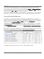
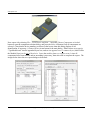
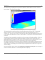
www.symmic.net
SYMMIC™ Application Note:
Flip Chip Solution using Export
™
SYMMIC: Template-Based Thermal Simulator for Monolithic Microwave Integrated Circuits
is a trademark of CapeSym, Inc.
Copyright © 2012 by CapeSym, Inc. All rights reserved.
www.symmic.net
1
Flip Chip Solution using Export
Flip chips require a slightly different approach for solution than bottom-mounted devices, due to the
different boundary conditions used. Typically a layout is used to model a chip, and SYMMIC uses linear
superposition to solve layouts of devices. This method allows very large problems to be solved directly and
efficiently (i.e. with matrix inversion instead of iteratively). The current implementation (version 2.7.0) of
this method makes assumptions about the boundary conditions which are unsuitable for flip chip types of
analyses, so flip chips can only be solved as a single template (no layouts). This limitation may be removed
in a future release, but in the mean time the Export feature makes it easy to create the single flip chip
template required. This application note describes how to configure and export a set of templates for a flip
chip type of analysis in two different ways, and how to create a flip chip suitable for equivalent thermal
impedance network calculation. It also highlights some of the power of the Export feature for solutions in
general.
Creating a Solder Bump Template
The flip chip example described here begins with a layout of HBT devices and solder bumps. These solder
bumps are what the chip will be mounted on once it is flipped.
To create a solder bump template to use in a flip chip layout, we begin with a very simple device, the Mesa
Resistor template. A number of changes are necessary; many can be done using the Device Template Editor
built into SYMMIC, whereas all can be done with a plain text editor. This note will use a mixture of both
approaches.
To begin, start SYMMIC and open the MesaResistor.xml template. Open the Device Template Editor with
File > Edit device template... From the Edit menu, delete the first three layers: Edit > Delete > Layers...
“Layer1” to “Layer3”. These operations remove the Adhesive, Shim and Solder layers, leaving just the
Substrate and top (bump) layers. (If this flip chip will have a heat sink mounted to its back side, then don't
delete these layers.)
Next find the parameter Z5 (“Mesa Thickness” in the Parameters folder, double-click the folder to open it)
and change its min and max values to “1” and “2000” (or larger), respectively (double-click the value very
slowly, then type the new number). Change its name to “Solder Bump Thickness” and its description
accordingly.
For parameters P2 and P3, remove “Backside” from their names. Finally, find the parameter Dbound and
reduce its min to “1” (this value is somewhat arbitrary, but it shouldn't be so small as to yield a bad mesh)
and change its description to “Width of boundary around the solder bump.”
Find the component called “Mesa” (in the Components folder) and rename it to “Solder Bump.” Also,
change the title of the entire template to “Solder Bump for a Flip Chip” and delete the help file name.
Select Device > Apply then quit and the display will show the updated device. Change the bump material to
Copyright © 2012 by CapeSym, Inc. All rights reserved.
www.symmic.net
2
Solder (Device > Components > Solder Bump = Au80Sn20), and the bump thickness to 500 microns
(Device > Thicknesses > Solder Bump Thickness = 500). Finally, save this new template as
“solderBump_FlipChip.xml.” The “FlipChip” in the name signifies that this template is for Export only, as
will be explained.
The next set of changes will be made with a plain text editor (e.g. Notepad, TextPad, or EditPlus), so open
the template just saved in your editor of choice. Go to the bottom of the file and replace the entire Boundary
Conditions section with the following (a film on the top of the bump).
<BoundaryConditions>
<Film h="P3" temperature="P2" face="top" layer="Layer5" toExport="1"
extractable="true" >
<Blocks x="2-3" y="2-3" />
</Film>
</BoundaryConditions>
Next, replace the string "Z1+Z2+Z3" with "0" in the ZLayers section, after which you can safely delete all
three of those parameters (Z1, Z2 and Z3). Also, delete the unused parameters NZ1, NZ2, NZ3, P0, P1,
P43, P45 and P46. Replace “Backside BC” in the name field of the derived parameters BC1W and BC1L
with “Template,” and their descriptions accordingly.
Change the names of parameters DX and DY to “Bump Length” and “Bump Width,” respectively, and
changes their descriptions accordingly, then save and exit your editor.
The template should now be complete.
Creating a Device Template for Flipping
The process for creating a flippable device has similarities to what was done for the solder bump, but the
boundary condition changes are different. In this case the back side boundary condition needs to be
removed (unless a heat sink will be attached, as before), but the device heating can stay in place. This
example will use the generic HBT template, but the same procedure could be applied to any device
template.
Open the HBT.xml template in SYMMIC, then open the Device Template Editor. Change the template's
title to “Half HBT for a Flip Chip.”
From the Edit menu, delete the first three layers: Edit > Delete > Layers... “layer00” to “layer02”. Select
Device > Apply to see the model update in the display. It should be left with just the Substrate layer,
matching the solder bump template.
The Export dialogs now allow the user to specify which components to include, so there is no need anymore
to explicitly set toExport flags. Simply select Device > Apply then quit and save the modified template as
“HBT_FlipChip.xml.”
Copyright © 2012 by CapeSym, Inc. All rights reserved.
www.symmic.net
3
As was done for the solder bump template, now open this template in your plain text editor of choice.
Search and replace the string "T00+T01+T02" with "0" (found in the ZLayers and Boundary Conditions
sections), after which you can safely delete all three of those parameters (T00, T01 and T02). Finally, delete
the unused parameters BFT and BFC. This completes the template.
Open the device template in SYMMIC and set up the dimensions, materials and powers to those required for
the simulation. If the layout will use different devices, then save each configuration with a unique name.
Create and Solve the Flip Chip Layout
As an example, we will solve a chip containing 4 solder bumps and 8 HBT's, making use of the chip's
symmetry to reduce the problem by half. To begin, start SYMMIC and load the new solder bump template.
In Device > Geometry... set the bump Width and Length to “200” and the Boundary Size to “20.” In Device
> Thicknesses... set the Solder Bump Thickness to “200” as well. Save these changes.
Then load the new HBT template. Set it up for 4 fingers (Device > Number of Fingers... “4”), and enable
the Emitter Bus Metal (Device > Optional Parts...). Set all three bus-to-boundary values to “2” (Device >
Lengths... Emitter Bus to Boundary; Device > Widths... Base Bus to Boundary, Collector Bus to Boundary),
then save the device.
Now select File > Create layout... and define a 4 x 1 array, starting at (150,500) and spaced at (100,0), with
mirroring in X. After creating the array, complete the layout as shown in the figure below.
The completed layout should look as follows. Save it as “HBT_FlipChip_layout.xml.”
Copyright © 2012 by CapeSym, Inc. All rights reserved.
www.symmic.net
4
Now export it by selecting File > Create device template... Select the Choose Components to Include
button to open the component-selection dialog, and press the Select All button if not all components are
selected. (Note that the device numbers are shown in the layout when this dialog displays to aid
identification, if necessary.) Choose OK to exit and return to the main dialog. Either browse to or type in
“TypeModule.xml” into the appended layers box, and set it to append lower 1 common layer (which will be
the Module1 layer) to the top of the device. Leave the smallest feature to resolve set at -1 since all
components have been retained and no smoothing is necessary, then select OK to complete the export. The
images below show the two export dialogs as described.
Copyright © 2012 by CapeSym, Inc. All rights reserved.
www.symmic.net
5
Open the exported template (“HBT_FlipChip_layout_export.xml”) and it should look similar to the layout,
but with an additional top layer appended onto the solder bumps as specified. On opening this template
SYMMIC will ask if you want to save changes to the devices and layout. The changes that it is referring to
are the default export settings, which it wants to update in both the device templates as well as in the layout
(i.e. to preserve the export settings just made). Select whichever option you prefer.
Load the new template into SYMMIC and reduce the thickness of the Module1 layer to 125 (Device >
Module Geometry > Appended Layer Module1 Thickness). Change this layer's material to Copper (Device
> Components, Module Attach, Cu), then the template should look like this.
Note that all of the HBT layers are still present, as well as all of the heating parameters for each of the
HBTs. If the template's Boundary Condition section is examined in a plain text editor, then a new Film
condition will be seen on top of the Module1 layer. The Film conditions on the solder bumps have been
removed. In addition, the SFLUX boundary conditions for the HBTs have been numbered from 1 to 4 using
the new dn flag.
After creating a template with Export, it is always a good idea to check the mesh resolution and adjust it if
needed, before beginning the solution. To do this, select Solve > Model check, Show mesh, and note the size
given in the console window. If it needs adjusting, the smallest mesh element size in X and Y as well as the
bias are given in Device > Meshing.
If the equivalent thermal impedance network is desired, select that check box in the Solve > Configure run
> RC calculations dialog, then save. Now the template is ready to solve; select Solve > Run simulation.
The solution will take longer if there is more than 1 device and the thermal impedance network is selected,
Copyright © 2012 by CapeSym, Inc. All rights reserved.
www.symmic.net
6
since it must solve everything twice for each device (turned on, while the others are all off – at their offpower settings). The solution is shown below.
The thermal network is stored in two forms, in the files with extension .BAS and .NET. If an unsteady
network is desired (i.e. an RC network instead of just the R), then set up an unsteady run (Solve >
Configure run > Simulation times) with very fine steps at the start and that lasts long enough for the devices
to reach steady-state temperatures, or nearly so, and run again. The network files will be updated with the C
component.
In conclusion, it bears repeating that a simulation is only as accurate as its boundary conditions. In the case
of the flip chip this means that accurate temperature boundary conditions for each solder bump or the
attached top layer(s) are essential. In many cases it will be necessary to solve the subsystem (e.g. the PCB
that the flip chip will mount to) first or even concurrently in order to get these temperatures.
For solutions of the entire subsystem for the purposes of obtaining accurate boundary conditions, the details
of each HBT are not needed. In cases such as these the mesh size and associated computation time can be
greatly reduced by not including most or all of the (unique) components shown in the Choose Components
To Include dialog.
For more information, please reference the Creating Device Templates From Layouts section of chapter 4
of the User's Manual, which lists a recommended procedure for flip chips.
Copyright © 2012 by CapeSym, Inc. All rights reserved.
www.symmic.net
7
For more information contact:
Matt Overholt
CapeSym, Inc.
6 Huron Drive
Natick, MA 01760 USA
Email: [email protected]
Tel: +1 508 653 7100 x204
Copyright © 2012 by CapeSym, Inc. All rights reserved.