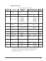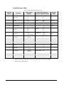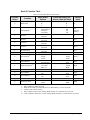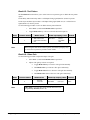
1
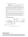
Ross Video Limited
ADC-8033A(-S)
Analog Component to SDI Video
Converter
User Manual
Ross Part Number: 8033ADR-004
Issue: 03
ADC-8033A(-S) • Analog Component to SDI Video Converter User Manual
•
•
•
Ross Part Number: 8033ADR-004
Document Issue: 03
Printed in Canada.
The information contained in this User Manual is subject to change without notice or obligation.
Copyright
© 2007 Ross Video Limited. All rights reserved.
Contents of this publication may not be reproduced in any form without the written permission of Ross
Video Limited. Reproduction or reverse engineering of copyrighted software is prohibited.
Notice
The material in this manual is furnished for informational use only. It is subject to change without
notice and should not be construed as a commitment by Ross Video Limited. Ross Video Limited
assumes no responsibility or liability for errors or inaccuracies that may appear in this manual.
Trademarks
•
•
•
is a registered trademark of Ross Video Limited.
Ross, ROSS, ROSS ®, and MLE are registered trademarks of Ross Video Limited.
All other product names and any registered and unregistered trademarks mentioned in
this manual are used for identification purposes only and remain the exclusive property
of their respective owners.
Important Regulatory and Safety Notices
Before using this product and any associated equipment, refer to the “Important Safety Instructions”
listed below so as to avoid personnel injury and to prevent product damage.
Products may require specific equipment, and /or installation procedures be carried out to satisfy
certain regulatory compliance requirements. Notices have been included in this publication to call
attention to these Specific requirements.
Symbol Meanings
This symbol on the equipment refers you to important operating and maintenance
(servicing) instructions within the Product Manual Documentation. Failure to heed
this information may present a major risk of damage or injury to persons or
equipment.
Warning
Caution
Notice
The symbol with the word “Warning” within the equipment manual indicates a
potentially hazardous situation, which if not avoided, could result in death or serious
injury.
The symbol with the word “Caution” within the equipment manual indicates a
potentially hazardous situation, which if not avoided, may result in minor or
moderate injury. It may also be used to alert against unsafe practices.
The symbol with the word “Notice” within the equipment manual indicates a
situation, which if not avoided, may result in major or minor equipment damage or a
situation which could place the equipment in a non-compliant operating state.
This symbol is used to alert the user that an electrical or electronic device or
assembly is susceptible to damage from an ESD event.
ESD
Susceptibility
Important Safety Instructions
Caution
This product is intended to be a component product of the RossGear 8000 series
frame. Refer to the RossGear 8000 series frame User Manual for important safety
instructions regarding the proper installation and safe operation of the frame as well
as it’s component products.
Warning
Certain parts of this equipment namely the power supply area still present a safety
hazard, with the power switch in the OFF position. To avoid electrical shock,
disconnect all A/C power cords from the chassis' rear appliance connectors before
servicing this area.
Warning
Service barriers within this product are intended to protect the operator and service
personnel from hazardous voltages. For continued safety, replace all barriers after
any servicing.
This product contains safety critical parts, which if incorrectly replaced may present
a risk of fire or electrical shock. Components contained within the product’s power
supplies and power supply area, are not intended to be customer serviced and should
be returned to the factory for repair.
To reduce the risk of fire, replacement fuses must be the same type and rating.
Only use attachments/accessories specified by the manufacturer.
EMC Notices
US FCC Part 15
This equipment has been tested and found to comply with the limits for a class A Digital device,
pursuant to part 15 of the FCC Rules. These limits are designed to provide reasonable protection
against harmful interference when the equipment is operated in a commercial environment. This
equipment generates, uses, and can radiate radio frequency energy and, if not installed and used in
accordance with the instruction manual, may cause harmful interference to radio communications.
Operation of this equipment in a residential area is likely to cause harmful interference in which case
users will be required to correct the interference at their own expense.
Changes or modifications to this equipment not expressly approved by Ross Video
Ltd. could void the user’s authority to operate this equipment.
Notice
CANADA
This Class “A” digital apparatus complies with Canadian ICES-003.
Cet appareil numerique de classe “A” est conforme à la norme NMB-003 du Canada.
EUROPE
This equipment is in compliance with the essential requirements and other relevant provisions of CE
Directive 93/68/EEC.
INTERNATIONAL
This equipment has been tested to CISPR 22:1997 along with amendments A1:2000 and A2:2002 and
found to comply with the limits for a Class A Digital device.
This is a Class A product. In domestic environments this product may cause radio
interference in which case the user may have to take adequate measures.
Notice
Maintenance/User Serviceable Parts
Routine maintenance to this RossGear product is not required. This product contains no user
serviceable parts. If the module does not appear to be working properly, please contact Technical
Support using the numbers listed under the “Error! Reference source not found.” section on the last
page of this manual. All RossGear products are covered by a generous 5-year warranty and will be
repaired without charge for materials or labor within this period. See the “Warranty and Repair
Policy” section in this manual for details.
Environmental Information
The equipment that you purchased required the extraction and use of natural resources for its
production. It may contain hazardous substances that could impact health and the environment.
To avoid the potential release of those substances into the environment and to diminish the need for
the extraction of natural resources, Ross Video encourages you to use the appropriate take-back
systems. These systems will reuse or recycle most of the materials from your end-of-life equipment in
an environmentally friendly and health conscious manner.
The crossed-out wheeled bin symbol invites you to use these systems.
If you need more information on the collection, reuse, and recycling systems, please contact your local
or regional waste administration.
You can also contact Ross Video for more information on the environmental performances of our
products.
Contents
Introduction
1-1
In This Chapter .......................................................................................................................1-1
A Word of Thanks....................................................................................................1-1
Overview ..................................................................................................................1-1
Functional Block Diagram .......................................................................................1-2
Features ....................................................................................................................1-3
Documentation Terms ..............................................................................................1-4
Abbreviations ...........................................................................................................1-4
Installation and Setup
2-1
In This Chapter .......................................................................................................................2-1
Static Discharge........................................................................................................2-1
Unpacking ................................................................................................................2-1
Board Installation .....................................................................................................2-2
BNC Labels ..............................................................................................................2-2
Cable Connections....................................................................................................2-2
User Controls
3-1
In This Chapter .......................................................................................................................3-1
User Controls............................................................................................................3-1
Function Select Switch.............................................................................................3-2
Mode Select Switch..................................................................................................3-2
Bootload Button .......................................................................................................3-2
Status and Selection LEDs .......................................................................................3-3
Using Banks
4-1
In This Chapter .......................................................................................................................4-1
General Operating Rules ..........................................................................................4-1
Selecting Banks ........................................................................................................4-2
Function Tables ........................................................................................................4-2
Using Bank A Functions ..........................................................................................4-6
Using Bank B Functions.........................................................................................4-11
Timing Modes ........................................................................................................4-14
Timing Modes Summary........................................................................................4-15
Input/Output Timing...............................................................................................4-17
Tracking Delay Pulse .............................................................................................4-17
Using Bank C Functions.........................................................................................4-17
ADC-8033A(-S) User Manual (Iss. 03)
Contents • i
Upgrades
5-1
In This Chapter ...................................................................................................................... 5-1
Equipment Supplied ................................................................................................ 5-1
Record Settings........................................................................................................ 5-2
Upgrade Procedures ................................................................................................ 5-4
Confirm Upgrade..................................................................................................... 5-6
Specifications
6-1
Technical Specifications ........................................................................................................ 6-1
Service Information
7-1
In This Chapter ...................................................................................................................... 7-1
Troubleshooting Checklist....................................................................................... 7-1
Warranty and Repair Policy .................................................................................... 7-2
Ordering Information
8-1
ADC-8033A(-S) and Related Products.................................................................................. 8-1
ii • Contents
ADC-8033A(-S) User Manual (Iss. 03)
Introduction
In This Chapter
This chapter contains the following sections:
• A Word of Thanks
• Overview
• Functional Block Diagram
• Features
• Documentation Terms
• Abbreviations
A Word of Thanks
Congratulations on choosing the Ross Video ADC-8033A(-S) Analog Component to SDI Video
Converter. You have purchased a powerful, versatile, and advanced converter. The ADC-8033A is
part of a full line of Digital Conversion Products within the RossGear Terminal Equipment family of
products, backed by our experience in engineering and design expertise since 1974.
You will be pleased at how easily your new ADC-8033A(-S) fits into your overall working
environment. Equally pleasing is the product quality, reliability and functionality. Thank-you for
joining the group of worldwide satisfied Ross Video customers!
Should you have a question pertaining to the installation and operation of your ADC-8033A, please
contact us at the numbers listed in this publication. Our technical support staff is always available for
consultation, training, or service.
Overview
The ADC-8033A(-S) is the perfect solution for converting analog component (YUV/RGB) sources
such as VTRs, cameras and character generators for use in the digital realm.
The component YUV/RGB video signal, with or without setup, is converted to four SDI 4:2:2
(SMPTE-259M) outputs with the highest level of precision. This is achieved because all signal
processing and color space conversion is performed in the digital domain. A two times over-sampled
12-bit A-D conversion and high quality digital filtering ensure superb frequency response.
ADC-8033A(-S) User Manual (Iss. 03)
Introduction • 1-1
The ADC-8033A(-S) is available in two different models:
•
ADC-8033A ⎯ The base model converter includes Proc Amp, Line Delay, and Line
Synchronizer modes.
•
ADC-8033A-S ⎯ The “S” model includes Frame Delay and Frame Synchronizer
modes, along with all the features available on the ADC-8033A(-S).
The ADC-8033A-S version comes with a full featured frame synchronizer, capable of synchronizing
incoming video to house reference. Various timing modes are available to accommodate most
situations. New techniques in frame synchronization contribute to the low power requirements and
compact design. The complete circuit for the ADC-8033A-S, including color space converter, frame
(or line) synchronizer, serializer, tracking delay pulse, three 12-bit A-D converters and a
microprocessor are all contained on a single DA-sized card. Additional daughter cards are not
required.
Operating status and function controls are all accessible on the front edge on the card. To simplify
configuration, a Heads-Up Display is provided. When enabled it is super-imposed over all card
outputs.
The ADC-8033A(-S) fits into the Ross 8000 series digital frames, with four cards in the DFR-8104A
(1RU), and up to ten cards in the DFR-8110A (2RU). Please refer to the frame User Manual for
specific ventilation and cooling instructions to maintain optimum operating conditions. This card also
fits into Leitch* FR-6800 series frames to provide you with greater installation versatility.
The ADC-8033A(-S) converters are part of a full line of RossGear digital distribution products
engineered to satisfy the highest quality broadcast standards and the most demanding requirements of
your facility.
Functional Block Diagram
Figure 1. Simplified Block Diagram of ADC-8033A(-S) Functions
* Leitch is a trademark of Leitch Technology Corporation
1-2 • Introduction
ADC-8033A(-S) User Manual (Iss. 03)
Features
The following features make the ADC-8033A(-S) the most flexible, high-quality conversion card for
your analog to digital conversion requirements:
•
YUV input from Betacam, MII and SMPTE/EBU formats
•
All RGB input formats supported
•
Four serial digital outputs
•
12-bit analog to digital conversion
•
2x over-sampling for excellent frequency response
•
Automatic 525/625 line selection
•
Can pass vertical interval signals
•
Programmable vertical interval blanking
•
Compact design on a single DA-sized card
•
Heads-Up Display
•
Optional Frame Synchronization (no daughter card required)
•
Field-upgradeable Frame Synchronization option available
•
Extensive Proc Amp controls
•
Freeze modes
•
Horizontal and vertical timing adjustments
•
Setup adjustment
•
Black level offset
•
Pass or clip Super Black
•
Status indicator LEDs on card edge
•
Choice of input timing source
•
Choice of reference inputs
•
Tracking Delay Output for companion audio synchronizer
•
Built-in test signals (FF color bars, SDI Checkfield)
•
10 modules fit in a 2RU frame
•
Fits Ross Video 8000 series digital products frames
and Leitch FR-6800 series frames
•
5-year transferable warranty
ADC-8033A(-S) User Manual (Iss. 03)
Introduction • 1-3
Documentation Terms
The following terms are used throughout this guide:
•
“Frame” refers to the DFR-8104A and DFR-8110A frames that house the ADC8033A(-S) card.
•
All references to the DFR-8104A and DFR-8110A also include the
DFR-8104A-C and DFR-8110A-C versions with the cooling fan option. Refer to
the respective User Manuals for details.
•
“Operator” and “User” both refer to the person who uses the ADC-8033A(-S).
•
“Board”, “Card”, and “Module” all refer to the ADC-8033A(-S) module itself.
•
“System” and “Video system” refers to the mix of interconnected production and
terminal equipment in which the ADC-8033A(-S) operates.
Abbreviations
The following abbreviations may be used throughout the text:
1-4 • Introduction
Abbreviation
Definition
ADC
A-D
D-A
DA
DAC
DDR
DIS
DVR
EN
LOW SIG
RU
SDI
VCR
VTR
Analog to Digital Converter
Analog-to-Digital
Digital-to-Analog
Distribution Amplifier
Digital to Analog Converter
Digital Disk Recorder
Disable
Digital Video Recorder
Enable
Low Signal
Rack Unit
Serial Digital Interface
Video Cassette Recorder
Video Tape Recorder
ADC-8033A(-S) User Manual (Iss. 03)
Installation and Setup
In This Chapter
This chapter contains the following information sections:
•
Static Discharge
•
Unpacking
•
Board Installation
•
BNC Labels
•
Cable Connections
Static Discharge
Whenever handling the ADC-8033A(-S) and other related equipment, please observe all static
discharge precautions as described in the following note:
ESD
Susceptibility
Static discharge can cause serious damage to sensitive
semiconductor devices. Avoid handling circuit boards in high
static environments such as carpeted areas, and when wearing
synthetic fiber clothing. Always exercise proper grounding
precautions when working on circuit boards and related
equipment.
Unpacking
Unpack each ADC-8033A(-S) you received from the shipping container, and check the contents
against the packing list to ensure that all items are included. If any items are missing or damaged,
contact your sales representative or Ross Video directly.
ADC-8033A(-S) User Manual (Iss. 03)
Installation and Setup • 2-1
Board Installation
Use the following procedure to install the ADC-8033A(-S) in a RossGear 8000 series digital
distribution frame:
•
Refer to the User Manual of the RossGear 8000 series frame, to ensure that the frame is
properly installed according to instructions. If this module is to be installed in any
compatible frame other than a Ross Video product, refer to the frame manufacturer’s
manual for specific instructions.
Heat and power distribution requirements within a frame may dictate
specific slot placement of cards. Cards with many heat-producing
components should be arranged to avoid areas of excess heat build-up,
particularly in frames using convectional cooling..
Note
•
After selecting the desired frame installation slot, hold the ADC-8033A(-S) card by the
edges and carefully align the card edges with the slots in the frame. Then fully insert the
card into the frame until the rear connection plug is properly seated.
BNC Labels
Affix the supplied BNC label, as per the included instructions, to the BNC area on the rear of the rack
frame.
Cable Connections
This section provides instructions for connecting cables to the ADC-8033A(-S) when mounted in
RossGear 8000 series Digital Products Frames. See the following frame rear panel diagram for BNC
input and output designations:
Figure 2. ADC-8033A(-S) BNC Designations for RossGear Frames
2-2 • Installation and Setup
ADC-8033A(-S) User Manual (Iss. 03)
User Controls
In This Chapter
This section contains a description of the ADC-8033A(-S) user controls.
Note
The ADC-8033A(-S) uses card edge controls for changing operational
parameters. The card defaults with switch access set to the locked position.
Refer to the “Bank A-F: Switch Access” section in Chapter 4, “Using
Banks”, before attempting to make any adjustments.
User Controls
The following are general descriptions of the user controls identified in the figure below.
Figure 3. Card-edge User Controls
ADC-8033A(-S) User Manual (Iss. 03)
User Controls • 3-1
Function Select Switch
The Function Select switch is a 16-position rotary switch used to select functions such as proc amp
controls and timing adjustment menu items. The switch works in conjunction with the Mode Select
toggle switch; first, the function category is selected, and then the toggle switch is used to select
modes or configuration settings within that function selection. See Chapter 4, “Using Banks” for
complete details.
Mode Select Switch
The Mode Select switch is used to enable, disable, and select specific ADC-8033A(-S) functional
modes, or configurations, within the operational function menu (selected first with the Function
Select switch). The Mode Select switch is a 3-position momentary toggle switch with an automatic
spring-return to the center position.
There are two methods of toggling to select basic and advanced level menu items:
•
Single toggle to select single options.
•
Hold toggle to scroll through multiple values or options.
Toggling the switch for menu selection is made according to two basic menu design categories:
•
Menu selections utilizing a scrolling wrap-around style of selection (from last menu
item directly back to first menu item).
•
Menu selections utilizing a bi-directional style of selection, with upper and lower
range limits.
Bootload Button
This button is used to upgrade the ADC-8033A(-S) software or firmware. Refer to Chapter 5,
“Upgrades” for complete details on the Bootload process.
3-2 • User Controls
ADC-8033A(-S) User Manual (Iss. 03)
Status and Selection LEDs
The front edge of the card features LEDs that display the status of the card, and indicate menu function
and configuration selections.
As selections are made from the menu tables, (Refer to Chapter 4, “Using Banks” for complete bank
menu table descriptions), the LEDs display the status of the input signals, as well as menu bank
selections. Basic LED displays and descriptions are provided in the following table:
Table 1. Selection and Status LED Descriptions
LED
Color
Display and Description
When lit, the card is functioning normally and no anomalies have been detected.
The following conditions must be satisfied:
• A valid input signal is present.
• A valid input timing signal is present (see Bank A-4).
• A valid reference signal is present when a reference is required, and
that the reference standard matches the input standard. Selecting
Line Sync or Frame Sync modes require that a reference signal is
present.
INPUT
OK
Green
ERROR
Red
BANK A
Green
When lit, Bank A is selected.
BANK B
Green
When lit, Bank B is selected.
BANK C
Green
When lit, Bank C is selected.
YUV
Green
When lit, the input signal is selected to be YUV in Bank A-2.
RGB
Green
When lit, the input signal is selected to be RGB in Bank A-2.
IN 525
Green
When lit, the input timing signal is 525.
IN 625
Green
When lit, the input timing signal is 625.
REF OK
Green
When lit, this LED indicates a reference signal is present and that the reference signal
is locked.
• On = External reference standard matches the input standard
• Flashing = External reference standard does not match the input standard
• Off = No external reference is present
FREEZE
Yellow
When lit, this LED indicates that the output is frozen (ADC-8033A-S only).
ACCESS
Yellow
When lit, this LED indicates that Switch Access is unlocked. Bank A, B, and C menu
functions are accessible.
When lit, conditions for INPUT OK are not met.
Mutually exclusive with INPUT OK.
ADC-8033A(-S) User Manual (Iss. 03)
User Controls • 3-3
3-4 • User Controls
ADC-8033A(-S) User Manual (Iss. 03)
Using Banks
In This Chapter
This section provides a detailed explanation on using Bank functions. The following topics are
discussed:
•
General Operating Rules
•
Selecting Banks
•
Function Tables
•
Using Bank A Functions
•
Using Bank B Functions
•
Using Bank C Functions
•
Timing Modes
•
Input/Output Timing
•
Tracking Delay Pulse
General Operating Rules
Please note the following important operating rules for the ADC-8033A(-S):
•
Note
Whenever the card is powered up, it defaults to Bank A, and the Bank A LED is lit.
The card defaults with switch access set to the locked position.
To unlock the access refer to the “Bank A-F: Switch Access”
section on page 4-10 before attempting to make any
adjustments.
•
For each of the supported video formats (SMPTE/EBU, MII, Betacam and NTSC
related in RGB/YUV) the card stores the default or user-adjusted video settings
independently in non-volatile memory. The selection of settings is determined by
the Video Standard Bank A-2.
•
Always check to see that the Input OK LED is lit. If not, check that the input is
valid, and that a valid input timing signal is present as per Bank A-4. If a reference
is used, check that the reference is valid and that the reference standard matches the
input standard.
ADC-8033A(-S) User Manual (Iss. 03)
Using Banks • 4-1
Before making adjustments, choose the method that you wish to use. Two methods are available:
1.
No Display ⎯ Adjustments are made using the Function Select and Mode Select
switches, without the assistance of the Heads-Up Display. Results should be confirmed
with test equipment suitable for measuring the parameter being adjusted (such as a
waveform monitor or vector scope).
2.
Heads-Up Display ⎯ Adjustments are made using Function Select and Mode Select
switches in conjunction with the Heads-Up Display. Ensure that the Heads-Up Display
is enabled (Bank A-1). Note that the display is superimposed over all ADC-8033A(-S)
video outputs.
Operating Conventions For Function Tables
The following rules apply to the function tables that are used throughout this section:
•
The label “ + ” instructs you to toggle the Mode Select switch (SW2) up momentarily.
•
The label “ - ” instructs you to toggle the Mode Select switch (SW2) down momentarily.
•
The label “ + (h) ” instructs you to hold the Mode Select switch (SW2) up for one
second or more.
•
The label “ - (h) ” instructs you to hold the Mode Select switch (SW2) down for one
second or more.
Selecting Banks
Function Select switch functionality is divided into three banks of functions. Use the following
procedure to select Bank A, B or C as required:
1.
Rotate Function Select (SW1) to position 0. Note that position 0 is always used to
select the bank, regardless of the bank that you are currently using.
2.
Toggle Mode Select (SW2) up or down to choose the desired bank. Three positions are
available: Bank A, B, or C.
3.
The table below illustrates each switch function, along with the Heads-Up Display label,
the Status LED indication, and the default value. If you are not using a display, be sure
to verify your selection on the Status LEDs.
Table 2. Switch and Bank Selection
Mode Select
+
-
Heads-Up Display Label
Status LED
A
BANK A
BANK A
B
BANK B
BANK B
C
BANK C
BANK C
Default Bank
A
Function Tables
This section presents a detailed charting of all board-level ADC-8033A(-S) functions in the following
three tables. The operational usage is explained in the next section.
Note
4-2 • Using Banks
Functions, as listed in the Function column as being stored in memory,
always power up in the last known state. All other items, however, power
up in the default state, regardless of their previous state.
ADC-8033A(-S) User Manual (Iss. 03)
Bank A Function Table
Table 3. Function Select: Bank A Function Table
Function
Select
Mode Select
Options
Function
+
0
1
2
BANK
-
A
B
C
+ (h)
-
On
Off
+
A
HEADS UP
ON
OFF
OFF
YUV BETA
YUV MII
YUV SMPTE
RGB NTSC
RGB MII
RGB SMPTE
IN STD
YUV BETA
YUV MII
YUV SMPTE
RGB NTSC
RGB MII
RGB SMPTE
YUV BETA
Frame
BNC 5
Y/G
IN TIMING
FRM
BNC 5
Y/G
Y/G
PATH
FF BARS
OFF
OFF
-
SDI Check Field
TEST PTN
Full Field Color Bars
Off
Input Video Standard m
-
3
N/A
4
Input Timing m
+
+
5
Default
Value
A
B
C
Bank Select
Heads-Up Display
Heads-Up Display OnScreen Label and Value
Test Pattern
6
N/A
7
N/A
8
Video Gain m
+
-
Increase
Decrease
VID GAIN
(###.#)%
9
Black Level Offset m
+
-
Increase
Decrease
BLK OFF
(##.#) IRE
A
Chroma Gain m
+
-
Increase
Decrease
CHROMA
(###.#)%
B
N/A
C
CB Gain m
+
-
Increase
Decrease
CB GAIN
(###.#)%
D
N/A
E
Factory Defaults
+ (h)
- (h)
Reset All
Reset Proc Amp
DEFAULT
ALL RST
PROC RST
N/A
F
Switch Access **
+
- (h)
Locked
Unlocked
ACCESS
LOCKED
UNLOCKED
LOCKED
100.0% *
0.0 IRE *
100.0% *
100.0% *
* Indicates Proc Amp controls that are affected by position E, Factory Defaults function.
** Locking Switch Access shuts off the Heads-up Display. Unlocking will not restore
the display if it was previously enabled. This must be performed manually.
m
Stored in non-volatile memory
ADC-8033A(-S) User Manual (Iss. 03)
Using Banks • 4-3
Bank B Function Table
Table 4. Function Select: Bank B Function Table
Function
Select
Mode Select
Options
Function
+
0
BANK
-
A
B
C
Setup m
+
-
On
Off
2
N/A
3
VI Blanking m
+
-
4
VI End m
+
Default
Value
A
B
C
A
SETUP
ON
OFF
ON *
Blank
Pass Through
VI BLANK
BLANK
PASS
PASS
VI END
21
20
19
19
-
21
20
19
Bank Select
1
Heads-Up Display OnScreen Label and Value
5
SuperBlack m
+
-
Clip
Pass Through
SUPER BLK
CLIP
PASS
PASS
6
V Bit Location m
(525 only)
+
-
Line 20
Line 10
V BIT LOC
20
10
20
7
N/A
8
N/A
9
N/A
A
H Crop m
+
-
On
Off
H CROP
ON
OFF
OFF
B
Crop Left m
+
-
Increase
Decrease
CROP LEFT
(##)
C
Crop Right m
+
-
Increase
Decrease
CROP RIGHT
(##)
D
N/A
E
N/A
F
N/A
*
m
4-4 • Using Banks
8
8
Indicates Proc Amp controls that are affected by position E, Factory Defaults function.
Stored in non-volatile memory
ADC-8033A(-S) User Manual (Iss. 03)
Bank C Function Table
Table 5. Function Select: Bank C Function Table
Function
Select
Mode Select
Options
Function
+
0
H DELAY
A
B
C
FS
FD
LS
LD
(####)
H RESET
ZERO
V DELAY
(###)
V RESET
ZERO
MIN DELAY
ZERO
FREEZE MODE
-
Frame
Field 2
Field 1
Freeze **
Pass Through
Freeze ** ‡
No Output
Black ***
FRM
FLD 2
FLD 1
ON
OFF
FRZ
NONE
BLK
+
+
-
On
Off
On
Off
FORCE BLK
+
-
BNC 5
Frame
REF SELECT
Bank Select
+
1
m
Timing Mode
+
+
+
+
+
m
2
H Delay
3
H Reset
4
V Delay
5
V Reset
6
Set Min. Delay
7
N/A
8
Freeze Mode
m
+
m
9
Forced Freeze
A
Input Timing Loss
B
N/A
C
Forced Black
m
D
Forced Mono
m
E
N/A
F
Reference Select
m
m
A
B
C
Frame Sync *
Frame Delay *
Line Sync
Line Delay
Increase
Decrease
Zero
No action
Increase
Decrease
Zero
No action
Zero
No action
Heads-Up Display OnScreen Label and Value
+
+
BANK
TIME MODE
FORCE FREEZE
IN TMG LOSS
FORCE MONO
Default
Value
A
LS
(FS on S
model)
0
N/A
0
N/A
N/A
ON
OFF
ON
OFF
FLD 1
OFF
BLK
OFF
OFF
BNC 5
FRM
FRM
*
**
Only available on ADC-8033A-S.
When Freeze mode is activated the freeze is determined by C-8 (Freeze Mode).
m
Stored in non-volatile memory
‡
Only available in Frame Sync Timing Mode and only if a valid reference is present.
*** Only available in Frame or Line Sync Timing Modes and only if a valid reference is present.
ADC-8033A(-S) User Manual (Iss. 03)
Using Banks • 4-5
Using Bank A Functions
The following topics are discussed in this section:
•
Heads-Up Display
•
Input Video Standard
•
Input Timing
•
Test Pattern
•
Video Gain
•
Black Level Offset
•
Chroma Gain
•
CB Gain
•
Factory Defaults
•
Switch Access
The card defaults with switch access set to the locked position.
To unlock the access, refer to “Bank A-F: Switch Access”
before attempting to make any adjustments.
Important
Bank A-1: Heads-Up Display
Use the following procedure to enable or disable the Heads-Up Display:
Bank
1.
Select Bank A, and rotate Function Select to position 1.
2.
Choose the desired display mode:
Function Select
A
Note
4-6 • Using Banks
1
•
Hold Mode Select up for one second to enable the display.
•
Toggle Mode Select down to disable the display.
Mode Select
+ (h)
-
On
Off
Heads-Up Display Label
HEADS UP
ON
OFF
Default
OFF
The display is superimposed over all ADC-8033A(-S) video
outputs. Do not use this feature with “on-air” signals.
ADC-8033A(-S) User Manual (Iss. 03)
Bank A-2: Input Video Standard
The Input Video Standard function allows you to select from six input video standards.
Use the following procedure to select a video standard:
Bank
1.
Select Bank A, and rotate Function Select to position 2.
2.
Toggle Mode Select up or down to select from the available video standards.
Function Select
Mode Select
+
A
2
-
YUV BETA
YUV MII
YUV SMPTE
RGB NTSC
RGB MII
RGB SMPTE
Heads-Up Display Label
IN STD
YUV BETA
YUV MII
YUV SMPTE
RGB NTSC
RGB MII
RGB SMPTE
Default
YUV BETA
Bank A-4: Input Timing
The Input Timing function selects where the input signal timing will come from.
Normally, the card obtains synchronization from the Y or G channel of the input signal. However, if
the input does not contain sync, an external sync source must be used. The timing of any external
reference must be ± 1µs relative to the normal position of sync on the input signal.
Use the following procedure to select a timing source:
1.
Select Bank A, rotate Function Select to position 4.
2.
Toggle Mode Select up or down to select from the available timing sources.
Bank
Function Select
A
4
Mode Select
+
-
Important
Frame
BNC 5
Y/G
Heads-Up Display Label
IN TIMING
FRM
BNC 5
Y/G
Default
Y/G
Setting both Input Timing (bank A-4 ) and Reference Select
(bank C-F) to the same source disables the synchronizing
operation of the ADC-8033A-S. Refer to “Input/Output
Timing” on page 4-17 for further details.
ADC-8033A(-S) User Manual (Iss. 03)
Using Banks • 4-7
Bank A-5: Test Pattern
The Test Pattern function allows you to select from two test pattern types or disable the test pattern
option.
In Line Delay and Frame Delay modes a valid Input Timing signal (Bank A-4) must be present.
In Line Sync and Frame Sync modes a valid Input Timing signal (Bank A-4) or a valid reference
signal (Bank C-F) must be present.
Use the following procedure to select or disable the test pattern function:
1.
Select Bank A, and rotate Function Select to position 5.
2.
Toggle Mode Select up or down to select the desired test pattern.
Bank
Function Select
A
5
Mode Select
+ SDI Check Field
Full Field Color Bars
- Off
Heads-Up Display Label
TEST PTN
PATH
FF BARS
OFF
Default
OFF
When using the SDI Check Field test pattern, the Heads-Up Display must
be Off for the test pattern to provide accurate results.
Note
Bank A-8: Video Gain
Use the following procedure to adjust the output video gain:
1.
Select Bank A, and rotate Function Select to position 8.
2.
Adjust video gain up or down as required:
Bank
Function Select
A
8
Note
4-8 • Using Banks
•
Toggle Mode Select up to increase video gain incrementally.
•
Hold Mode Select up to increase video gain continuously.
•
Toggle Mode Select down to decrease video gain incrementally.
•
Hold Mode Select down to decrease video gain continuously.
Mode Select
+
-
Increase
Decrease
Heads-Up Display Label
VID GAIN
(###.#)%
Default
100%
Video Gain is one of the Proc Amp controls that can be reset
using Factory Defaults (Bank A-E).
ADC-8033A(-S) User Manual (Iss. 03)
Bank A-9: Black Level Offset
This setting is a black level offset that is not affected by the Setup function (Bank B-1). For example,
with Black Level Offset at 1 IRE, a setup level of 7.5 IRE, and Setup off, the black level will be 8.5
IRE. With Setup on and a setup level of 7.5 IRE, the black level will be 1.0 IRE.
Use the following procedure to change the output black level:
1.
Select Bank A, and rotate Function Select to position 9.
2.
Choose the desired Black Level Offset setting:
Bank
Function Select
A
9
Note
•
Toggle Mode Select up to increase the black level offset incrementally.
•
Hold Mode Select up to increase the black level offset continuously.
•
Toggle Mode Select down to decrease the black level offset incrementally.
•
Hold Mode Select down to decrease the black level offset continuously.
Mode Select
+
-
Increase
Decrease
Heads-Up Display Label
BLK OFF
(##.#) IRE
Default
0 IRE
Black Level Offset is one of the Proc Amp controls that can be
reset using Factory Defaults (Bank A-E).
Bank A-A: Chroma Gain
Use the following procedure to adjust the output chroma gain:
1.
Select Bank A, and rotate Function Select to position A.
2.
Adjust chroma gain up or down as required:
Bank
Function Select
A
A
Note
•
Toggle Mode Select up to increase chroma gain incrementally.
•
Hold Mode Select up to increase chroma gain continuously.
•
Toggle Mode Select down to decrease chroma gain incrementally.
•
Hold Mode Select down to decrease chroma gain continuously.
Mode Select
+
-
Increase
Decrease
Heads-Up Display Label
CHROMA
(###.#)%
Default
100%
Chroma Gain is one of the Proc Amp controls that can be
reset using Factory Defaults (Bank A-E).
ADC-8033A(-S) User Manual (Iss. 03)
Using Banks • 4-9
Bank A-C: CB Gain
Use the following procedure to adjust the ADC-8033A(-S)’s output CB gain:
1.
Select Bank A, and rotate Function Select to position C.
2.
Adjust CB Gain up or down as required:
Bank
Function Select
A
C
•
Toggle Mode Select up to increase CB gain incrementally.
•
Hold Mode Select up to increase CB gain continuously.
•
Toggle Mode Select down to decrease CB gain incrementally.
•
Hold Mode Select down to decrease CB gain continuously.
Mode Select
+
-
Increase
Decrease
Heads-Up Display Label
CB GAIN
(###.#)%
Default
100%
CB Gain is one of the Proc Amp controls that can be reset
Note
using Factory Defaults (Bank A-E).
Bank A-E: Factory Defaults
This function allows you to return all controls to their default values, or simply the four “Proc Amp”
controls by themselves.
Use the following procedure to select factory default values:
Bank
1.
Select Bank A, and rotate Function Select to position E.
2.
Select the desired default settings:
Function
Select
A
•
Hold Mode Select up for one second to reset all adjustments to their default
values.
•
Hold Mode Select down for one second to reset the “Proc Amp”
adjustments to their default values (Video Gain, Black Level Offset,
Chroma Gain, and CB Gain).
Mode Select
+ (h)
- (h)
E
Reset All
Reset Proc Amp
Heads-Up Display Label
DEFAULT
ALL RST
PROC RST
Default
N/A
Bank A-F: Switch Access
The Switch Access function allows you to lock or unlock user access to all adjustment parameters.
The “lock” function should be performed after installation to secure all settings, and to prevent anyone
from accidentally changing the settings. Note the following rules:
4-10 • Using Banks
•
When access is locked, all menu items are locked, no adjustments can be made and
the Heads-Up Display is automatically turned off.
•
When you unlock switch access and you wish to use the Heads-Up Display, you
must manually enable it (Bank A-1).
ADC-8033A(-S) User Manual (Iss. 03)
Use the following procedure to lock or unlock switch access:
1.
Select Bank A, and rotate Function Select to position F.
2.
Choose the desired access mode:
Bank
Function Select
A
F
•
Toggle Mode Select up to lock switch access. Adjustments cannot be
made, and the display is disabled. The ACCESS LED is off.
•
Hold Mode Select down for one second to unlock switch access.
Adjustments can now be made. The ACCESS LED is on.
Mode Select
+
- (h)
Locked
Unlocked
Heads-Up Display Label
ACCESS
LOCKED
UNLOCKED
Default
LOCKED
Using Bank B Functions
The following topics are discussed in this section:
•
Setup
•
Vertical Interval Blanking
•
Vertical Interval End
•
SuperBlack
•
Vertical Bit Location
•
Horizontal Line Crop
•
Horizontal Line Crop Left
•
Horizontal Line Crop Right
Bank B-1: Setup
If your analog input video has setup, it must be removed in order for the ADC-8033A(-S) to convert it
to valid SDI output. Use this function to remove any setup that may exist on the analog input signal.
1.
Select Bank B, and rotate Function Select to position 1.
2.
Choose the desired setup value:
Bank
Function Select
B
1
ADC-8033A(-S) User Manual (Iss. 03)
•
Toggle Mode Select up to remove setup from the input signal.
•
Toggle Mode Select down if there is no setup on the input signal.
Mode Select
+
-
On
Off
Heads-Up Display Label
SETUP
ON
OFF
Default
OFF
Using Banks • 4-11
Bank B-3: Vertical Interval Blanking
Use the following procedure to blank the vertical interval, or allow the signals in the vertical interval
to pass through the ADC-8033A(-S). The last line of the vertical interval is set in Bank B-4.
1.
Select Bank B, and rotate Function Select to position 3.
2.
Choose the desired blanking mode:
Bank
Function Select
B
3
•
Toggle Mode Select up to blank the vertical interval.
•
Toggle Mode Select down to pass the vertical interval.
Mode Select
+
-
Heads-Up Display Label
Blank
VI BLANK
Pass Through
BLANK
PASS
Default
PASS
Bank B-4: Vertical Interval End
In 525 mode, the ADC-8033A(-S) has a programmable Vertical Interval that allows you to set where
the VI ends. The line chosen in this function is considered the last line in the Vertical Interval.
Video setup is not removed in the vertical interval even if the
Setup Bank (B-1) is set to ON.
Note
Use the following procedure to select the end point for vertical blanking:
Bank
1.
Select Bank B, and rotate Function Select to position 4.
2.
Toggle Mode Select up or down to select the desired vertical interval end.
Function Select
Mode Select
Heads-Up Display Label
+
B
21
VI END (##)
20
19
* 525 – line mode
** 625 – line mode, value fixed at 22
4
21
20
19
Default
19*
or
22**
Bank B-5: SuperBlack
Use the following procedure to enable or disable the SuperBlack clipping function:
1.
Select Bank B, and rotate Function Select to position 5.
2.
Choose the desired SuperBlack setting:
Bank
Function Select
B
5
•
Toggle Mode Select up to clip any value below black.
•
Toggle Mode Select down to allow the active input signal to pass through
unaltered.
Mode Select
+
-
Clip
Pass Through
Heads-Up Display Label
SUPER BLK
CLIP
PASS
Default
PASS
Bank B-6: V Bit Location
Use the following procedure to force the V bit to be asserted on line 10 or line 20.
4-12 • Using Banks
ADC-8033A(-S) User Manual (Iss. 03)
Note
V Bit Location is only available in 525. V-BIT LOC cannot be
changed in 625.
1.
Select Bank B, and rotate Function Select to position 6.
2.
Choose the desired line:
Bank
Function Select
B
6
•
Toggle Mode Select up to have the V bit set to line 20.
•
Toggle Mode Select down to have the V bit set to line 10.
Mode Select
+
-
Line 20
Line 10
Heads-Up Display Label
V BIT LOC
20
10
Default
20
Bank B-9: Horizontal Line Crop
The active video portion of an SDI video line is wider than that of an analog component video line.
The smaller active analog video is centered on that of the SDI video. Use this card to crop the leading,
the trailing, or both video samples on the output SDI video line. This will avoid possible errors
downstream if converting back to analog component video.
Use the following procedure to enable or disable horizontal line cropping.
1.
Select Bank B, and rotate the Function Select to position 9.
2.
Toggle the Mode Select up or down to select the desired cropping option.
Bank
Function Select
B
9
Mode Select
+
-
On
Off
Heads-Up Display Label
H CROP
ON
OFF
Default
OFF
Bank B-A: Horizontal Crop Left
The output SDI video line can be cropped starting at the beginning of the line in increments of one
pixel up to 350.
Use the following procedure to select the desired number of pixels cropped.
1.
Select Bank B, and rotate Function Select to position A.
2.
Toggle Mode Select up or down to select the desired number of pixels cropped.
Bank
Function Select
B
A
Mode Select
+
-
Increase
Decrease
Heads-Up Display Label
CROP LEFT
(#)
Default
8
Bank B-B: Horizontal Crop Right
The output SDI video line can be cropped from the end of the line backwards toward the beginning of
the line in increments of one pixel up to 350.
Use the following procedure to select the desired number of pixels cropped.
1.
Select Bank B, and rotate Function Select to position B.
2.
Toggle Mode Select up or down to select the desired number of pixels cropped.
ADC-8033A(-S) User Manual (Iss. 03)
Using Banks • 4-13
Bank
Function Select
B
B
Mode Select
+
-
Increase
Decrease
Heads-Up Display Label
CROP RIGHT
(#)
Default
8
Timing Modes
The ADC-8033A and ADC-8033A-S offer two sets of timing modes; Line Delay/Sync and Frame
Delay/Sync.
ADC-8033A Timing Mode Features
•
Line Delay and Line Sync timing modes
•
Two lines of memory
•
Can be timed within one line in 37ns increments
•
Can be field-upgraded to the Frame Sync version
ADC-8033A-S Timing Mode Features
•
Frame Delay and Frame Sync as well as Line Delay and Line Sync timing modes
•
One frame of memory
•
Can be timed within one frame in 37ns increments
Line Delay (ADC-8033A & ADC-8033A-S)
Line Delay mode uses the signal selected in bank A-4 to generate the output timing. There is a
constant delay between the input and the output. The external reference is not used. This is useful in
applications where a constant delay through the card is required.
The delay through the card has a minimum value, as described in Chapter 6, “Specifications”. Output
timing can be adjusted from this minimum delay up to an additional two lines in half-pixel increments.
Line Sync (ADC-8033A & ADC-8033A-S)
Line Sync mode uses the external reference to generate the output timing on a line-by-line basis, but
uses the timing from the signal selected in Bank A-4 to decide when a frame begins.
Whenever a signal is received, the output-timing generator waits for the next falling edge of H Sync
on the external reference before displaying the incoming line. The advantage of this mode is that as
long as all input sources are timed to be on the same line, the output timing stays constant, regardless
of which input is selected. This is very useful in that all sources to the ADC-8033A(-S) (for example,
from a routing switcher) only need to be lined up to the same line.
The Line Sync mode has internal latency, so that using minimum delay still means that the output
video will not be lined up with the external reference. To do so would have added even more latency,
which would not be desirable. However, output timing can be delayed by up to two lines from the
minimum delay point on, in half-pixel increments, so that the output video can be lined up as required.
4-14 • Using Banks
ADC-8033A(-S) User Manual (Iss. 03)
Note
If two input sources are not on the same line, then switching
from one source to the other causes a jump in the output timing
by an exact number of lines. For example, if the two sources
are 2.5 lines apart, the output will jump by either 2 or 3 lines
depending on the position of the sources with respect to the
external reference.
Threshold Point
As the input signal is delayed in time, there comes a point where the output timing will have
to jump by exactly one line (the output must always come after the input). This point is
called the threshold point. In 525 line video format, when comparing the input signal with
the external reference, the threshold point is 1.9 microseconds after the falling edge of the
external reference. In other words, if the falling H sync edge of the input signal is 1.9
microseconds after the falling H sync edge of the external reference, the input signal is said to
be on the threshold. In 625 line video formats, the threshold point is at 1.6microseconds.
In addition, there is built in hysteresis so that if an input source is near the threshold point, the
output timing will be constant and will not jump back and forth by a line if the input signal
varies slightly. However, if the input signal is exactly on the threshold point, the output
timing may vary from one power up sequence to the other. In other words, the card may
power up with different timing than the previous time it was powered-up. To avoid this
condition, it is recommended to keep the input signal away from the threshold point. Two
microseconds can be considered a safe distance.
Note
In Line Sync mode, you should keep the falling sync edge of
the incoming video away from the threshold point.
Frame Delay (ADC-8033A-S)
The Frame Delay mode is identical to the Line Delay mode, except that the output timing can be
delayed by up to a full frame of video. By using almost a full frame of delay, it is possible to set
apparent negative timing, making it look like the output occurs before the input, although delayed by
one frame.
Frame Sync (ADC-8033A-S)
The Frame Sync mode makes it possible to use asynchronous sources. The output timing is generated
entirely based on the external reference. Whether a synchronous or an asynchronous source is used,
output timing is constant. The delay range through the card will be from the minimum processing
delay (in the order of microseconds) up to a full frame.
Timing Modes Summary
This section provides a summary of all Timing Modes.
Line Delay
Use when you do not have a -S version and need constant delay through the card.
•
Output timing based on the Input Timing Menu (A-4)
•
Ignores external reference
•
Has the lowest minimum delay through the card
•
Two-line output timing adjustment window
ADC-8033A(-S) User Manual (Iss. 03)
Using Banks • 4-15
Line Sync
Use when you do not have a -S version and need constant output timing even though input timing may
change. This is the recommended mode for the non-S version.
•
Output timing based on external reference (line by line only)
•
If input sources are timed to be on the same line, the output timing will be constant
•
Keep input timing away from the threshold point
Frame Delay
Use when you have a -S version and need constant delay through the card.
•
Output timing based on Input Timing menu (A-4)
•
Ignores external reference
•
Has the lowest minimum delay through the card
•
Output timing adjustment window has infinite phasing over a full frame
Frame Sync
Use when you have a -S version and need constant output timing, or when the input is asynchronous to
house reference.
4-16 • Using Banks
•
Input can be asynchronous
•
Output timing is constant, regardless of input timing
•
Output phasing is infinite over a full frame, and the delay through the card varies
from a minimum of one field to a maximum of three fields.
ADC-8033A(-S) User Manual (Iss. 03)
Input/Output Timing
The most common use of the ADC-8033A(-S) model is to convert an asynchronous analog component
source to house referenced SDI. In this case the analog component source is clocked into the card
with the sync source selected in Input Timing Menu (A-4) and the output is clocked out of the card
relative to a house reference source selected in Reference Select Menu (C-F).
For the purposes of this timing discussion, the ADC-8033A(-S) is split up into input and output
sections. The input timing refers to how the card times input analog component signals. The output
timing refers to how the output SDI serial stream is clocked.
Input timing is usually obtained from the G/Y channel of the input signal, on BNC IN. If the input G/Y
signal does not contain sync then the user can input an analog timing signal into either BNC 5 or the
Frame Reference. The BNC 5 or Frame Reference input timing selection is made in menu A-4. The
ADC-8033A(-S) must have a valid input timing source (e.g. locked and timed to the INPUT signal) to
operate correctly.
The output timing is obtained from an analog reference signal, input either into BNC 5 or the Frame
Reference. The BNC 5 or Frame Reference output timing selection is made in menu C-F. If there is no
valid output timing source, the ADC-8033A-S will use the input timing source for output timing.
Note
If the same source is selected for both the input and output
timing, then the SDI output stream will be timed to the input
analog component signal. In this case the synchronizing
feature of the ADC-8033A-S will not work. The card will
default to Line Delay mode even if it is set to Line Sync mode,
and Frame Delay mode even if it is set to Frame Sync mode.
Tracking Delay Pulse
The ADC-8033A-S offers a positive 5V tracking delay output that pulses at frame rate on BNC 6. The
pulse width is a measurement of the video delay through the card. This is useful when connecting with
devices which accept this type of measurement signal, such as the RossGear ADL-8520 AES Audio
Delay module. Typically, this pulse is useful when operating in Frame Delay or Frame Sync Timing
Modes only.
Using Bank C Functions
The following topics are discussed in this section:
•
Timing Mode
•
Horizontal Delay
•
Horizontal Delay Reset
•
Vertical Delay
•
Vertical Delay Reset
•
Set Minimum Delay
•
Freeze Mode
•
Forced Freeze
•
Input Timing Loss
•
Forced Black
•
Forced Monochrome
•
Reference Select
ADC-8033A(-S) User Manual (Iss. 03)
Using Banks • 4-17
Bank C-1: Timing Mode
Use the following procedure to set the timing mode:
1.
Select Bank C, and rotate Function Select to position 1.
2.
Select the desired timing mode according to the following table.
•
Bank
Toggle Mode Select up or down to select the desired timing mode.
Function Select
Mode Select
+
C
Frame Sync *
Frame Delay *
Line Sync
Line Delay
1
-
Heads-Up Display Label
TIME MODE
FS
FD
LS
LD
Default
LS
(FS on -S
models)
* Indicates ADC-8033A-S only
In Frame Sync mode, the ADC-8033A-S buffers slightly less
than a full frame of signal in memory to allow any input
variation to be corrected on the output.
Note
Bank C-2: Horizontal Delay
Use the following procedure to adjust the output Horizontal Delay:
1.
Select Bank C, and rotate Function Select to position 2.
2.
Increase or decrease the Horizontal Delay as required:
Bank
Function Select
C
2
•
Toggle Mode Select up to increase Horizontal Delay by half a pixel (one
27MHz-clock period) with each toggle.
•
Hold Mode Select up to increase Horizontal Delay continuously.
•
Toggle Mode Select down to decrease Horizontal Delay by half a pixel
(one 27MHz-clock period) with each toggle.
•
Hold Mode Select down to decrease Horizontal Delay continuously.
Mode Select
+
-
Increase
Decrease
Heads-Up Display Label
H DELAY
(#)
Default
0
Please note the following important points regarding Horizontal Delay:
•
If you cross over the maximum Horizontal Delay, the value returns to 0 (zero) and
the Vertical Delay value increments by 1.
•
Crossing the minimum delay returns the Horizontal Delay value to 1715 (525) or
1725 (625) and decrements the Vertical Delay value by 1.
Crossing from 0 to maximum or from maximum to 0 will affect
the Vertical Delay setting in Bank C-4.
Note
Bank C-3: Horizontal Delay Reset
Use the following procedure to reset just the Horizontal Delay value to 0 (zero). This function is
particularly useful if your adjustment range is far off the mark, or if you simply want to quickly return
to zero.
4-18 • Using Banks
ADC-8033A(-S) User Manual (Iss. 03)
1.
Select Bank C, and rotate Function Select to position 3.
2.
Reset Horizontal Delay as required:
•
Bank
Function Select
C
3
Toggle Mode Select up to reset Horizontal Delay to 0.
Mode Select
+
-
Zero
No action
Heads-Up Display Label
H RESET
ZERO
Default
N/A
Bank C-4: Vertical Delay
Use the following procedure to adjust the output Vertical Delay:
1.
Select Bank C, and rotate Function Select to position 4.
2.
Increase or decrease the Vertical Delay as required:
Bank
Function Select
C
4
•
Toggle Mode Select up to increase Vertical Delay by one line, and wrap
around from the maximum to 0 if necessary.
•
Hold Mode Select up to increase Vertical Delay continuously.
•
Toggle Mode Select down to decrease Vertical Delay by one line, and wrap
around from 0 to the maximum if necessary.
•
Hold Mode Select down to decrease Vertical Delay continuously.
Mode Select
+
-
Increase
Decrease
Heads-Up Display Label
V DELAY
(#)
Default
0
Bank C-5: Vertical Delay Reset
Use the following procedure to reset just the Vertical Delay value to 0 (zero).
1.
Select Bank C, and rotate Function Select to position 5.
2.
Reset Vertical Delay as required:
•
Bank
Function Select
C
5
Toggle Mode Select up to reset Vertical Delay to 0.
Mode Select
+
Zero
No action
Heads-Up Display Label
V RESET
ZERO
Default
N/A
Bank C-6: Set Minimum Delay
Use the following procedure to reset both the Horizontal Delay and Vertical Delay values to 0 (zero).
1.
Select Bank C, and rotate Function Select to position 6.
2.
Reset all delays as required:
•
Bank
Function Select
C
6
ADC-8033A(-S) User Manual (Iss. 03)
Toggle Mode Select up to reset Horizontal Delay and Vertical Delay to 0.
Mode Select
+
-
Zero
No action
Heads-Up Display Label
MIN DELAY
ZERO
Default
0
Using Banks • 4-19
Bank C-8: Freeze Mode
The input image can be frozen (ADC-8033A-S only) if any of the following conditions occur:
•
The user manually freezes the input (Forced Freeze, Bank C-9).
•
There is a loss of the input timing signal (Input Timing Loss, Bank C-A).
The Freeze Mode function allows you to set what will be output when a freeze occurs: the last Field 1,
the last Field 2, or the last Full Frame. Use the following procedure to set the Freeze Mode:
1.
Select Bank C, and rotate Function Select to position 8.
2.
Toggle Mode Select up or down to select the desired Freeze Mode.
Bank
Function Select
C
8
Mode Select
+
-
Frame
Field 2
Field 1
Heads-Up Display Label
FREEZE MODE
FRM
FLD 2
FLD 1
Default
FLD 1
Bank C-9: Forced Freeze
The output can be manually frozen (ADC-8033A-S only) using the Forced Freeze mode. When
enabled, the freeze will use either field 1, field 2 or the entire frame (as determined by the Freeze
Mode function, Bank C-8).
Use the following procedure to enable or disable the Forced Freeze mode:
1.
Select Bank C, and rotate Function Select to position 9.
2.
Select the desired mode:
Bank
Function Select
C
9
•
Toggle Mode Select up to freeze the image. The FREEZE LED is on.
•
Toggle Mode Select down to un-freeze the image, and allow input video to
pass through. The FREEZE LED is off.
Mode Select
+
-
Freeze
Pass
Through
Heads-Up Display Label
FORCE FREEZE
ON
OFF
Default
OFF
Bank C-A: Input Timing Loss
Use this function to select what type of video appears at the four outputs when the Input Timing signal
(Bank A-4) is lost or invalid. These choices are available:
•
Black - SDI black.
•
No Output - flat line, no signal present.
•
Freeze - the last valid image is automatically frozen (ADC-8033A-S only).
The freeze is determined by the Freeze Mode function (Bank C-8).
Use the following procedure to set the Input Timing Loss:
Bank
1.
Select Bank C, and rotate Function Select to position A.
2.
Toggle Mode Select up or down to select the desired Input Timing Loss option.
Function Select
4-20 • Using Banks
Mode Select
Heads-Up Display Label
Default
ADC-8033A(-S) User Manual (Iss. 03)
+
C
A
-
Freeze ** ‡
No Output
Black ***
IN TMG LOSS FRZ
NONE
BLK
BLK
** When Freeze mode is activated the freeze is determined by C-8 (Freeze Mode).
‡
Only available in Frame Sync Timing Mode and only if a valid reference is present.
*** Only available in Frame or Line Sync Timing Modes and only if a valid reference is present.
Bank C-C: Forced Black
Use this selection to force the output to SDI black.
In Line Delay and Frame Delay modes a valid Input Timing signal (Bank A-4) must be present.
In Line Sync and Frame Sync modes a valid Input Timing signal (Bank A-4) or a valid reference
signal (Bank C-F) must be present.
Use the following procedure to enable or disable the Forced Black mode:
1.
Select Bank C, and rotate Function Select to position C.
2.
Select the desired mode according to the table below:
Bank
Function Select
C
C
•
Toggle Mode Select up to force the output to SDI black.
•
Toggle Mode Select down to disable the Forced Black mode.
Mode Select
+
-
On
Off
Heads-Up Display Label
FORCED BLK ON
OFF
Default
OFF
Bank C-D: Forced Mono
Use this selection to force the output to monochrome (SDI). Use the following procedure to enable or
disable the Forced Monochrome mode:
1.
Select Bank C, and rotate Function Select to position D.
2.
Select the desired mode according to the table below:
Bank
Function Select
C
D
•
Toggle Mode Select up to force the output to monochrome.
•
Toggle Mode Select down to disable the Forced Monochrome mode.
Mode Select
+
-
On
Off
Heads-Up Display Label
FORCED MONO
ON
OFF
Default
OFF
Bank C-F: Reference Select
Use the following procedure to select a reference input source:
1.
Select Bank C, and rotate Function Select to position F.
2.
Select the desired reference according to the table below:
ADC-8033A(-S) User Manual (Iss. 03)
•
Toggle Mode Select up to choose BNC 5 input.
•
Toggle Mode Select down to choose frame input.
Using Banks • 4-21
Bank
Function Select
F
Reference Select
Important
4-22 • Using Banks
Mode Select
+
-
BNC 5
Frame
Heads-Up Display Label
REF SELECT
BNC 5
FRM
Default
FRM
Setting both Input Timing (bank A-4 ) and Reference Select
(bank C-F) to the same source disables the synchronizing
operation of the ADC-8033A-S. See the “Input/Output
Timing” section on page 4-17 for further details.
ADC-8033A(-S) User Manual (Iss. 03)
Upgrades
In This Chapter
This chapter provides instructions to properly upgrade your ADC-8033A(-S) for the following:
•
Frame Synchronization Upgrade
•
Software Upgrade
•
Firmware Upgrade
To order any ADC-8033A(-S) Upgrade kit, contact Ross Video Technical Support.
This chapter contains the following sections:
•
Equipment Supplied
•
Record Settings
•
Upgrade Procedures
•
Confirm Upgrade
Equipment Supplied
•
1 ADC-8033A(-S) User Manual
•
Required upgrade chip(s)
ADC-8033A(-S) User Manual (Iss. 03)
Upgrades • 5-1
Record Settings
Before performing the upgrade, use the following tables to record the configurations and settings you
have selected in bank A, B, and C of the ADC-8033A(-S). The card must be reconfigured after the
upgrade is complete.
Table 6. Function Select: Bank A Function Table
SW1 Function
Select
Function
0
Bank Select
1
Heads-Up Display
2
Video Standard
3
N/A
4
Input Timing
5
Test Pattern
6
N/A
7
N/A
8
Video Gain
9
Black Level Offset
A
Chroma Gain
B
N/A
C
CB Gain
D
N/A
E
Factory Defaults
F
Switch Access
5-2 • Upgrades
Bank A Settings
ADC-8033A(-S) User Manual (Iss. 03)
Table 7. Function Select: Bank B Function Table
SW1 Function
Select
Function
0
Bank Select
1
Setup
2
N/A
3
VI Blanking
4
VI End
5
SuperBlack
6
V Bit Location
7
N/A
8
N/A
9
N/A
A
H Crop
B
Crop Left
C
Crop Right
D
N/A
E
N/A
F
N/A
Bank B Settings
Table 8. Function Select: Bank C Function Table
SW1 Function
Select
Function
0
Bank Select
1
Timing Mode
2
Horizontal Delay
3
Horizontal Delay Reset
4
Vertical Delay
5
Vertical Delay Reset
6
Set Min. Delay
7
N/A
8
Freeze Mode
9
Forced Freeze
A
Input Timing Loss
B
N/A
C
Forced Black
D
Forced Mono
E
N/A
F
Reference Select
ADC-8033A(-S) User Manual (Iss. 03)
Bank C Settings
Upgrades • 5-3
Upgrade Procedures
This section contains procedures for the following upgrade options:
•
Chip Removal
•
Frame Synchronizer Upgrade
•
Software or Firmware Upgrade
•
Confirm Frame Synchronizer Upgrade
•
Confirm Software or Firmware Upgrade
U7
Socket
Bootload
Button
Figure 4. ADC-8033A(-S) Upgrade Socket and Label Locations
Chip Removal
The three possible upgrades to the ADC-8033A(-S) all use socket U7. If there is a chip already
inserted into U7, remove it as in the following procedure:
5-4 • Upgrades
1.
Record your settings on the tables provided in the previous section.
2.
With the card out of the frame, refer to Figure 4 and the card labeling to locate chip
socket U7.
3.
Use a tong-type IC chip removal tool (not supplied) to grab the chip by the unlegged ends and gently pry the chip out of the socket.
4.
Store the chip in a labeled static free container. You may need to return it to the
socket later if it is a Frame Synchronizer upgrade chip. The card cannot operate as a
Frame Synchronizer without a synchronizer chip in the socket.
ADC-8033A(-S) User Manual (Iss. 03)
Frame Synchronizer Upgrade
1.
Remove the card from the frame.
2.
Verify the card issue level matches the issue level of the upgrade kit.
3.
Refer to Figure 4 and the card labeling to locate socket U7.
4.
If the socket is occupied, complete the Chip Removal procedure on the previous
page.
5.
Align the new chip over the socket with the keyed sides together and the legs over
the socket holes.
6.
Gently and firmly press the chip into the socket.
7.
Perform the Confirm Frame Synchronizer Upgrade procedure on the following page.
8.
Refer to the relevant chapters in this user manual for information on the operation of
the full frame synchronizer.
Software or Firmware Upgrade
This procedure applies to any software or firmware upgrade you may perform on the ADC-8033A(-S).
If you are upgrading multiple cards, repeat this procedure for each card to be upgraded.
1.
With the card out of the frame, refer to Figure 4 and the card labeling to locate the
U7 socket.
2.
If the socket is occupied, complete the Chip Removal procedure.
3.
Carefully remove the new chip from the packaging.
4.
Align the new chip over the socket with the keyed sides together and the legs over
the socket holes.
5.
Gently and firmly press the chip into the socket.
6.
Press the Bootload button while inserting the card into the powered frame and wait
for the upgrade to complete. Alternately, you can insert the card and power up the
frame if it is off.
When the green OK LED starts flashing, the upgrade is in progress and you can
release the Bootload button.
The OK LED will flash at various rates throughout the upgrade. The upgrade is done
when the LED stops flashing. Upgrades can take approximately 90 seconds to
complete.
7.
Complete the Confirm Software or Firmware Upgrade procedure on the following
page.
8.
Remove the card from the frame and complete the Chip Removal procedure on the
previous page.
9.
If your card had the Frame Synchronizer upgrade installed, you will have to reinstall
that chip using the Frame Synchronizer Upgrade procedure above.
ADC-8033A(-S) User Manual (Iss. 03)
Upgrades • 5-5
Confirm Upgrade
Depending on whether you upgraded to the Frame Synchronizer option or upgraded the card software
or firmware, use the relevant upgrade confirm procedure below.
Confirm Frame Synchronizer Upgrade
With the card installed in the frame and powered up:
1.
Rotate Function Select to the 0 position, toggle Mode Select to Bank A, and rotate
Function Select to position F.
2.
Hold Mode Select down for one second to unlock switch access.
The ACCESS LED is on.
3.
Rotate Function Select to position 1.
4.
Hold Mode Select up for one second to enable the Heads-Up Display.
5.
Rotate Function Select to position 0.
6.
Toggle Mode Select down to position C.
7.
Hold Mode Select down for several seconds to display the card model installed.
On the Heads-Up Display, “ADC-8033A-S” is displayed, indicating that the
upgrade was successful.
8.
If you are upgrading multiple cards, repeat the relevant upgrade procedures as
necessary.
Confirm Software or Firmware Upgrade
With the card installed in the frame and powered up:
1.
Rotate Function Select to the 0 position, toggle Mode Select to Bank A, and rotate
Function Select to position F.
2.
Hold Mode Select down for one second to unlock switch access.
The ACCESS LED is on.
3.
Rotate Function Select to position 1.
4.
Hold Mode Select up for one second to enable the Heads-Up Display.
5.
Rotate Function Select to position 0.
6.
Hold Mode Select up for several seconds to display the card software and hardware
versions installed.
On the Heads-Up Display, “SW V #.## HW V #.#” is displayed, indicating that the
upgrade was successful. Confirm that the displayed numbers match the upgrade
versions you have performed.
7.
5-6 • Upgrades
If you are upgrading multiple cards, repeat the relevant upgrade procedures as
necessary.
ADC-8033A(-S) User Manual (Iss. 03)
Specifications
Technical Specifications
Table 9. ADC-8033A(-S) - Technical Specifications
Category
Parameter
Specification
Analog
Component
Input
Number of Inputs
3 RGB/YUV
Input Impedance
75Ω
Return Loss
>42dB to 5MHz
Signal Standards
SMPTE 259M-C, 270Mb/s 525/625 lines
Number of Outputs
4
Output Impedance
75Ω
Output Return Loss
>18dB to 270MHz
Signal Level
800mV ± 10%
DC Offset
<40mV
Rise and Fall Time
>800pS (20 - 80%, ±15%)
Overshoot
<10% typical
Signal Standards Accepted
NTSC, PAL, Composite Sync (2V, 4V)
Number of Inputs
1
Input Impedance
75Ω
Return Loss
>40dB to 5MHz
Group delay
<5ns to 4.2MHz
RMS Noise, Luma Channel
>60dB to 5MHz unweighted
RMS Noise, Chroma Channels
>60dB to 5MHz unweighted
Quantization
12 bits
For Line/Frame Delay Mode
25.9µS
SDI Output
Analog
Reference
Performance
Minimum
Delay
ADC-8033A(-S) User Manual (Iss. 03)
Specifications • 6-1
Category
Parameter
Specification
Tracking
Delay Pulse
ADC-8033A-S
up to 2 video fields
Power
Consumption
Total
4.7W
Specifications are subject to change without notification
6-2 • Specifications
ADC-8033A(-S) User Manual (Iss. 03)
Service Information
In This Chapter
This chapter contains the following sections:
•
Troubleshooting Checklist
•
Warranty and Repair Policy
Troubleshooting Checklist
Routine maintenance to this RossGear product is not required. In the event of problems with your ADCthe following basic troubleshooting checklist may help identify the source of the problem. If
the module still does not appear to be working properly after checking all possible causes, please
contact your Ross Video products distributor, or the Ross Video Technical Support department at the
numbers listed under the “Contact Us” section at the end of this manual.
8033A(-S),
1.
A valid sync source must be present for Heads-Up Display and video output.
2.
Visual Review ⎯ Performing a quick visual check may reveal many problems, such
as connectors not properly seated or loose cables. Check the module, the frame, and
any associated peripheral equipment for signs of trouble.
3.
Power Check ⎯ Check the power indicator LED on the distribution frame front
panel for the presence of power. If the power LED is not illuminated, verify that the
power cable is connected to a power source and that power is available at the power
main. Confirm that the power supplies are fully seated in their slots. If the power
LED is still not illuminated, replace the power supply with one that is verified to
work.
4.
Reseat the Card in the Frame ⎯ Eject the card and reinsert it in the frame.
5.
Check Control Settings ⎯ Refer to the Installation and Operation sections of the
manual and verify all user settings.
6.
Input Signal Status ⎯ Verify that source equipment is operating correctly and that
a valid signal is being supplied.
7.
Output Signal Path – Verify that destination equipment is operating correctly and
receiving a valid signal.
8.
Module Exchange ⎯ Exchanging a suspect module with a module that is known to
be working correctly is an efficient method for localizing problems to individual
modules.
ADC-8033A(-S) User Manual (Iss. 03)
Service Information • 7-1
Warranty and Repair Policy
The ADC-8033A(-S) is warranted to be free of any defect with respect to performance, quality,
reliability, and workmanship for a period of FIVE (5) years from the date of shipment from our
factory. In the event that your ADC-8033A(-S) proves to be defective in any way during this warranty
period, Ross Video Limited reserves the right to repair or replace this piece of equipment with a unit
of equal or superior performance characteristics.
Should you find that this ADC-8033A(-S) has failed after your warranty period has expired, we will
repair your defective product for as long as suitable replacement components are available. You, the
owner, will bear any labor and/or part costs incurred in the repair or refurbishment of said equipment
beyond the FIVE (5) year warranty period.
In no event shall Ross Video Limited be liable for direct, indirect, special, incidental, or consequential
damages (including loss of profits) incurred by the use of this product. Implied warranties are
expressly limited to the duration of this warranty.
This ADC-8033A(-S) Analog Component to SDI Video Converter User Manual of our Digital
Products line provides all pertinent information for the safe installation and operation of your Product.
Ross Video policy dictates that all repairs to the ADC-8033A(-S) are to be conducted only by an
authorized Ross Video Limited factory representative. Therefore, any unauthorized attempt to repair
this product, by anyone other than an authorized Ross Video Limited factory representative, will
automatically void the warranty. Please contact Ross Video Technical Support for more information.
In Case of Problems
Should any problem arise with your ADC-8033A(-S), please contact the Ross Video Technical
Support Department. (Contact information is supplied at the end of this publication.)
A Return Material Authorization number (RMA) will be issued to you, as well as specific shipping
instructions, should you wish our factory to repair your ADC-8033A(-S). A temporary replacement
module, if required, will be made available at a nominal charge. Any shipping costs incurred, will be
the responsibility of you, the customer. All products shipped to you from Ross Video Limited, will be
shipped collect.
The Ross Video Technical Support Department will continue to provide advice on any product
manufactured by Ross Video Limited, beyond the warranty period without charge, for the life of this
equipment.
7-2 • Service Information
ADC-8033A(-S) User Manual (Iss. 03)
Ordering Information
ADC-8033A(-S) and Related Products
Your ADC-8033A(-S) Analog Component to SDI Video Converter is a part of the RossGear family of
products. Ross Video offers a full line of RossGear terminal equipment including distribution,
conversion, monitoring, synchronizers, encoders, decoders, AES, Keyers, switches, as well as analog
audio and video products
Standard Equipment
•
•
ADC-8033A Analog Component to SDI Video Converter
ADC-8033A-S Analog Component to SDI Video Converter with Frame
Synchronizer
Optional Equipment
•
•
•
•
•
•
8033ADR-004 Analog Component to SDI Video Converter
(additional User Manual)
EXT-8100 Extender Board
(module servicing extension)
DFR-8104A Digital Products Frame and Power Supply (PS-8102)
(1RU, holds 4 modules, includes 1 power supply)
DFR-8104A-C Digital Products Frame with Cooling Fan Module
and Power Supply (PS-8102)
(1RU, holds 4 modules, includes 1 power supply)
DFR-8110A Digital Products Frame and Power Supply (PS-8102)
(2RU, holds 10 modules, includes 1 power supply)
DFR-8110A-C Digital Products Frame with Cooling Fan Module
and Power Supply (PS-8102)
(2RU, holds 10 modules, includes 1 power supply)
.
ADC-8033A(-S) User Manual (Iss. 03)
Ordering Information• 8-1
Contact Us
Contact our friendly and professional support representatives for the following:
•
Name and address of your local dealer
•
Product information and pricing
•
Technical support
•
Upcoming trade show information
PHONE
E-MAIL
POSTAL
SERVICE
General Business Office
and Technical Support
613 • 652 • 4886
After-hours Emergency
613 • 349 • 0006
Fax
613 • 652 • 4425
General Information
[email protected]
Technical Support
[email protected]
Ross Video Limited
8 John Street,
Iroquois, Ontario, Canada
K0E 1K0
Ross Video Incorporated
P.O. Box 880,
Ogdensburg, New York, USA 136690880
Visit Us
Please visit us at our website for:
•
Company information
•
Related products and full product lines
•
On-line catalog
•
Trade show information
•
News
•
Testimonials