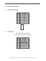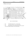
1
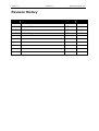
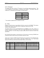
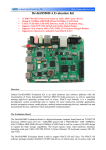
Version 1.2 Page 1 of 27 SMT339 User Manual V1.3 SMT339 User Manual V1.3 User Manual (QCF42); Version 1.2, 8/11/00; © Sundance Multiprocessor Technology Ltd. 1999 Version 1.2 Page 2 of 27 SMT339 User Manual V1.3 Revision History Date Comments Engineer Version 01/12/05 Initial Draft AJP 1.0 20/06/06 Second Draft AJP 1.1 03/07/06 Corrections AJP 1.2 21/12/06 Added Diagram of video connectors AJP 1.3 Version 1.2 Page 3 of 27 SMT339 User Manual V1.3 Table of Contents 1 Introduction ..................................................................................................................................... 6 2 Functional Description .................................................................................................................... 7 2.1 Block Diagram ........................................................................................................................ 7 2.2 Memory Map .......................................................................................................................... 8 2.2.1 DSP Memory Map.............................................................................................................. 8 2.2.2 Virtex 4 Memory Map......................................................................................................... 8 2.3 DSP Unit................................................................................................................................. 9 2.3.1 EMIF Peripheral Configuration .......................................................................................... 9 2.3.2 I2C Control........................................................................................................................ 10 2.4 Flash..................................................................................................................................... 10 2.5 SDRAM ................................................................................................................................ 11 2.6 Virtex 4 FPGA ..................................................................................................................... 12 2.6.1 2.6.1.1 LED Register ........................................................................................................... 13 2.6.1.2 Comports................................................................................................................. 13 2.6.1.3 Video Encoder Register .......................................................................................... 14 2.6.1.4 Video Decoder Register .......................................................................................... 14 2.6.1.5 High Speed Nt (ZBT) Memory................................................................................. 16 2.6.1.6 SLB Interface........................................................................................................... 16 2.6.2 2.7 3 SLB Power Supplies ........................................................................................................ 17 Video Encoder/Decoder ....................................................................................................... 18 Video Ports.................................................................................................................................... 19 3.1 Video Encoder Setup ........................................................................................................... 19 3.1.1 Video Memory.................................................................................................................. 20 3.1.2 EDMA............................................................................................................................... 21 3.2 4 Virtex 4 Peripherals.......................................................................................................... 12 3.1.2.1 RGB656 Single Bank EDMA Setup ........................................................................ 21 3.1.2.2 BT656 with embedded Sync EDMA Setup ............................................................. 21 Video Decoder Setup ........................................................................................................... 22 JTAG ............................................................................................................................................. 22 4.1 DSP JTAG Chain ................................................................................................................. 22 4.2 Virtex 4 JTAG chain ............................................................................................................. 22 5 SMT339 Video Input and Video Output Connections................................................................... 23 6 Using the SMT339 JTAG with TI Tools. ....................................................................................... 24 7 Firmware Upgrades ...................................................................................................................... 24 8 Power consumption ...................................................................................................................... 24 Version 1.2 9 10 Page 4 of 27 SMT339 User Manual V1.3 Cables and Connectors ................................................................................................................ 25 9.1 JP5 Virtex JTAG Header...................................................................................................... 25 9.2 JP7 Connector...................................................................................................................... 25 Where’s that Jumper?................................................................................................................... 27 Table of Figures Figure 1 : Block Diagram for SMT339..........................................................................7 Figure 2 : Flow from Video Memory to Encoder ........................................................19 Figure 3 : Video Memory organisation in YCbCr output mode...................................20 Figure 4 : RGB565 organisation of the video memory ...............................................21 Figure 5 : Jumper Finder Diagram .............................................................................27 Table of Tables Table 1 : Table of Abbreviations ..................................................................................5 Table 2 : DSP Memory Map ........................................................................................8 Table 3 : Virtex 4 Internal Peripherals..........................................................................8 Table 4 : EMIF Configurations .....................................................................................9 Table 5 : Virtex 4 LED Register bit Definitions ...........................................................13 Table 6 : Virtex 4, Video Encoder Register................................................................14 Table 7 : Virtex 4, Video Decoder Register................................................................14 Table 8 : Video Port 0 and Decoder connectivity .......................................................15 Table 9 : Video Port 0 and Decoder Clock connectivity .............................................15 Table 10 : Video Port 0 Decoder Data to Video Port Data Mapping ..........................15 Table of Abbreviations BAR Base Address Region DMA Direct Memory Access EPLD Electrically Programmable Logic Device PCI Peripheral Component Interconnect SDB Sundance Digital Bus Version 1.2 SRAM Page 5 of 27 Static Random Access Memory TBC Test Bus Controller TIM Texas Instruments Module Table 1 : Table of Abbreviations SMT339 User Manual V1.3 Version 1.2 Page 6 of 27 SMT339 User Manual V1.3 1 Introduction The SMT339 is a dedicated high speed image processing module for use in a wide range of image analysis systems. The module can be plugged into a standard TIM single width slot and can be accessed by either a standard Comport, or Rocket Serial Link (RSL) Interface. The image processing engine is based upon the ‘Texas Instruments’ TMS320DM642 Video Digital Signal Processor. It is fully software compatible with C64x using Code Composer Studio. The DM642 runs at a clock rate of 720MHz. It features a two level cache based architecture. There are 16K Bytes of level one program cache (Direct mapped), 16K Bytes of level one data cache (2-Way Set-Associative) and 256K Bytes of level two cache that is shared program and data space (Flexible RAM/Cache Allocation). The DM642 can perform 4, 16 x 16 Multiplies or 8, 8 x 8 Multiplies per clock cycle. A powerful Vitrex-4 FPGA (XC4VFX60-10) is used onboard as the FPGA processing unit for image data. 8 Mbytes of ZBT SRAM is provided as a FPGA memory resource. Processing functions such as Colour Space Conversion (CSC), Discrete Cosine Transforms (DCT), Fast Fourier Transforms (FFT) and convolution can be implemented, without using any of the DSP’s resources. If required, the Virtex 4 has 2 Power PC hardware cores that can be incorporated into the system design. The Module features a single ‘Philips Semiconductors’ SAA7109AE/108AE video decoder/encoder that accept most PAL and NTSC standards, and can output processed images in PAL/NTSC or VGA (1280x1024, or HD TV Y/Pb/Pr) The DM642 has 128 Mbytes of high speed SDRAM (Micron MT48LC64M32F2S5 ) available onboard for image processing and an 8Mbytes FLASH device is fitted to store programs and FPGA configuration information. The module supports a full Sundance LVDS Bus (SLB) interface for use with mezzanine cards providing the flexibility for other image formats to be accepted and other output formats to be generated. User Manual (QCF42); Version 1.2, 8/11/00; © Sundance Multiprocessor Technology Ltd. 1999 Version 1.2 Page 7 of 27 SMT339 User Manual V1.3 2 Functional Description The basic block diagram of the SMT339 and its components is illustrated in Figure 1. 2.1 Block Diagram Figure 1 : Block Diagram for SMT339 User Manual (QCF42); Version 1.2, 8/11/00; © Sundance Multiprocessor Technology Ltd. 1999 Version 1.2 2.2 Page 8 of 27 SMT339 User Manual V1.3 Memory Map The various addresses and lengths of the peripherals shown in Figure 1 are shown in Table 2. 2.2.1 DSP Memory Map Address (bytes) Length (Bytes) 0x0000 0000 Abbreviation Description INTRAM DSP Internal Memory 0x8000 0000 64MBytes EXTRAM External SDRAM 100MHz bus speed 0x9000 0000 8MBytes FLASH External FLASH Memory 0xA000 0000 --- VIRTEXMAP Virtex 4 Memory Area Table 2 : DSP Memory Map 2.2.2 Virtex 4 Memory Map Address (bytes) Length (Bytes) Abbreviation Description 0xA001 8000 4 Bytes COM2_DATA Communication Port 2 Data Register 0xA001 C000 4 Bytes COM2_STAT Communication Port 2 Status Register 0xA001 C000 4 Bytes COM3_DATA Communication Port 3 Data Register 0xA001 C000 4 Bytes COM3_STAT Communication Port 3 Status Register 0xA00D 0000 4 Bytes LED_REG LED Register 0xA00D 8000 4 Bytes VID_ENC_REG Video Encoder Register 0xA00E 0000 4 Bytes VID_DEC_REG Video Decoder Register 0xA00E 4000 4 Bytes SLB_CTRL_REG SLB Interface Control Register: Not Implemented in standard code. Table 3 : Virtex 4 Internal Peripherals Version 1.2 2.3 Page 9 of 27 SMT339 User Manual V1.3 DSP Unit As illustrated in Figure 1 the SMT339 is based around the ‘Texas Instruments’ TMS320DM642 Video Imaging Processor. The processor is based around the second generation VelociTI Texas Instruments TMS320C6000 generation of processors. This processor has 3 built-in video imaging ports (each 20 bit) which each have 2 channels capable of sample rates up to 80MHz over a 10 bit bus, the direction of each channel being configurable as input or output. This allows Images to be DMA’ed directly to the SDRAM for processing, while the processed image can be viewed on one of the output channels. Input YCbCr formats with embedded sync information can be accepted by the video ports as well as RAW data modes. See Chapter 3 for details of the Video port operation. The DM642 DSP has 128Mbytes of high speed SDRAM memory available for program and data space, an 8Mbyte FLASH allows FPGA configuring data and DSP program data to be stored. The DSP’s EMIF bus is also routed to the Virtex 4 FPGA, which allows the mapping of the Comports and the RSL directly into the DSP’s memory map. The EMAC, serial ports and Audio channels are routed from the DSP to the Virtex 4, this allows the EMAC, SLB or Audio physical interfaces to be added to the system if required. Software development and real-time debugging can be achieved using Code Composer Studio (Texas Instruments) via the JTAG interface. Full specifications for the DSP can be downloaded from http://focus.ti.com/lit/ds/symlink/tms320dm642.pdf 2.3.1 EMIF Peripheral Configuration The various peripherals are mapped into the DSP memory space into chip select spaces as illustrated in Table 4 . Peripheral DSP CS Area Base Address CE Space Control Register Value Description SDRAM CE0 0x8000 0000 0x0000 00D0 64 bit wide SDRAM Interface FLASH CE1 0x9000 0000 0xFFFF FF13 16 bit wide Asynchronous interface VIRTEX 4 CE2 0xA000 0000 0x0000 0030 32 bit wide SDRAM Interface VIRTEX 4 Configuration CE3 0xB000 0000 0xFFFF FF23 32 bit wide Asynchronous Interface Table 4 : EMIF Configurations Version 1.2 Page 10 of 27 SMT339 User Manual V1.3 2.3.2 I2C Control The DM642 DSP has a built-in I2C interface for controlling internal peripherals. This 2 wire serial bus is connected to 3 devices in the system. The devices and their respective I2C addresses are illustrated in the table below. Device Address (LSB ‘0’- wr ) Video Decoder 0x40 Video Encoder 0x88 Virtex 4 ** NA ** No interface implemented in standard firmware. 2.4 Flash 8Mbytes of flash memory is provided with direct access by the DM642. This device contains boot code for the DSP and the configuration data for the FPGA. This is a 16-bit wide device. The flash device can be re-programmed by the DM642 at any time. There is a software protection mechanism to stop most errant applications from destroying the device’s contents. For extra safety a jumper (JP1) must be inserted to allow write operations. Note that the flash memory is connected as a 16 bit device, but during a DM642 boot (internal function of the C6x) only the bottom 8 bits are used. There are a number of DSP General Purpose pins connected to the FLASH devices Bank Pins in order to allow access to the upper FLASH areas. The Table below shows the GPIO pins values and associated memory access areas. GPIO10 GPIO9 DSP Memory Address FLASH Access Address (16bit) 0 0 0x9000 0000 -> 0x900F FFFF 0x0000 0000 -> 0x000F FFFF 0 1 0x9000 0000 -> 0x900F FFFF 0x0010 0000 -> 0x001F FFFF 1 0 0x9000 0000 -> 0x900F FFFF 0x0020 0000 -> 0x002F FFFF 1 1 0x9000 0000 -> 0x900F FFFF 0x0030 0000 -> 0x003F FFFF Version 1.2 Page 11 of 27 SMT339 User Manual V1.3 For more detailed information on the programming of the FLASH see the manufacturer’s data sheet, Am29LV641D. 2.5 SDRAM There are128Mbytes of SDRAM connected to the DM642 processor via its external memory interface (EMIF). The EMIF clock runs at 100MHz and the bus width is 64bits, organized as 2 banks of 32bits. This allows a peak data transfer rate of 400Mbytes/second. Version 1.2 2.6 Page 12 of 27 SMT339 User Manual V1.3 Virtex 4 FPGA The FPGA on the SMT339 is a Virtex 4 FX60 device (XC4VFX6010FF1152). It is connected to the DSP’s EMIF and therefore allows its internal peripherals to be accessed at 100MHz clock rates and a bus width of 64bits. This allows high speed transfers to be initiated at request. It should, however, be noted that sustained large transfer will affect the DSP’s peak performance if the DSP’s algorithm is running in external SDRAM memory. To avoid this, the application can be run in internal DSP memory. Some of the FPGA’s features are listed below. • The Virtex-4 enhanced PowerPC™ 405 core delivers 680 DMIPS performance at 450 MHz and the new Auxiliary Processor Unit (APU) controller • 400+ MHz clock rates • 2.8Mbits of internal block RAM available. • Up to 444 18X18 embedded multipliers • Extensive library of DSP algorithms 2.6.1 Virtex 4 Peripherals The Standard firmware supplied with a SMT339 contains interfaces for the peripherals listed below. • Mapping of 2 Video Ports and related control registers • Mapping of 2 communication ports • LED Register Mapping • Video Encoder Control Register • Video Decoder Control Register Version 1.2 Page 13 of 27 SMT339 User Manual V1.3 2.6.1.1 LED Register There are 4 LEDS mapped in the Virtex 4 firmware that can be accessed via the DSP over the EMIF. The resister is located at 0xA00D0000 and is mapped as follows. D7 D6 D5 D4 D3 D2 D1 D0 X X X X LED D8 LED D7 LED D6 LED D5 Table 5 : Virtex 4 LED Register bit Definitions The location of the LED’s is shown in the figure below. LED D5 LED D6 LED D7 LED D8 2.6.1.2 Comports There are 2 Comports implemented in the standard FPGA configuration file. Comport 3 and Comport 2. Comport 3 is usually routed via the carrier module to the Host CPU for setup and control by 3L or other applications. See the SMT6400 for detailed operation of how they can be used. Version 1.2 Page 14 of 27 SMT339 User Manual V1.3 2.6.1.3 Video Encoder Register The Video Encoder Register (0xA00D 8000) in the Virtex 4 allows various firmware parameters to be setup correctly. By default Video Port 1 is connected to the video encoder. D7 D6 D5 D4 D3 D2 D1 D0 X X X D_MUX X TRI_C TVD ENC_RST Table 6 : Virtex 4, Video Encoder Register ENC_RST – Encoder Reset, when ‘1’ the Reset pin on the video decoder is active. TRI_C – When ‘0’ the Video port Control Lines (HSync and VSync) are driven by the Encoder. The Encoder is in Master Sync mode. When ‘1’ the Video Port Sync Pins are Tri-Stated. TVD – TV Detected. Read only bit that returns a 1 in a load is detected on the CVBS video output. D_MUX – When this bit is ‘0’ the Video Port D[9..2] is fed directly to the encoder pins D[7..0]. When set to a logic ‘1’ the data stream from the video port is assumed to be RGB656 and is de-multiplexed from the Lower 16 bits of the Video Port 1 before driving the encoder pins. 2.6.1.4 Video Decoder Register The Video Decoder Register (0xA00E 0000) in the Virtex 4 allows various firmware parameters to be setup correctly. By default Video Port 0 is connected to the video decoder. D7 D6 D5 D4 D3 D2 D1 D0 X X X X X CTRL_DIR CLK_DIR DEC_RST Table 7 : Virtex 4, Video Decoder Register DEC_RST – Decoder Reset, when ‘1’ the Reset pin on the video decoder is active. Version 1.2 Page 15 of 27 SMT339 User Manual V1.3 CLK_DIR – When ‘0’ the Video Port 0 clk0 and clk1 pins are both driven by the decoders pixel clock. When ‘1’ the Virtex pins are tri-stated. CTRL_DIR – Driving of the various Video 0 control signals. The tables below shows the state of video port control and data signals for different values of CTRL_DIR and CLK_DIR. CTRL_DIR ‘0’ Vp0_ctrl0 - ‘1’ (this mode used for embedded sync input) Vp0_ctrl1 - ‘1’ ‘1’ Vp0_ctrl2 - ‘Z’ Vp0_ctrl0 - Dec Hsync Vp0_ctrl1 - Dec Vsync Vp0_ctrl2 - Dec ODD Table 8 : Video Port 0 and Decoder connectivity CLK_DIR ‘0’ Vp0_clk0 - dec_pclk Vp0_clk1 - pclk ‘1’ Vp0_clk0 - ‘Z’ Vp0_clk1 - ‘Z’ Table 9 : Video Port 0 and Decoder Clock connectivity Video Port 0 Data Pins Video Decoder Data Pins VP0_D(19..12) Decoder_C(7 .. 0) VP0_D(11..10) ‘00’ VP0_D(9..2) Decoder_Y(7 .. 0) VP0_D(1..0) ‘00’ Table 10 : Video Port 0 Decoder Data to Video Port Data Mapping Version 1.2 Page 16 of 27 SMT339 User Manual V1.3 2.6.1.5 High Speed Nt (ZBT) Memory There is just over 8Mbytes of high speed, no turnaround, (Nt) SRAM is connected to the FPGA allowing high speed data storage capability to FPGA cores that require external memory. The memory is based on two separate Samsung K7N321801M devices which are each 2M by 18-bit devices, allowing independent access of each device Please contact us if you require further information on using this device. 2.6.1.6 SLB Interface The Sundance LVDS Bus (SLB) is a dual-port parallel interconnection link that is capable of supporting data transfers at up to 700 MHz. Each port can be assigned with a 16-bit differential bus, a clock and an over range differential lines. The SLB is a link for data and clocks but also for control signals; it is based on a Samtec QSH/QTH-DP series (0.5mm pitch) connectors. The use of the SLB means that other customer specific input or output methods can be supported without the need for re-design of the hardware. Some examples of IO interfaces are listed below. Input • Camera Link • Firewire • CMOS Sensor • Fiber Channel • DVI Output • USB • IDE • Fiber Channel • LCD/Plasma Display drivers • DVI Version 1.2 Page 17 of 27 SMT339 User Manual V1.3 The standard Virtex firmware does not contain any SLB interfacing. During manufacture the SLB connectors connectivity is tested. 2.6.2 SLB Power Supplies When using the SLB interface a separate SLB power header (BKT) is used to supply the Daughterboard. Details of this connector pinout can be found in the SLB Reference Guide. Version 1.2 2.7 Page 18 of 27 SMT339 User Manual V1.3 Video Encoder/Decoder The encoder/decoder is based on the ‘Philips Semiconductors’ SAA7109AE/108AE. This provides decoding of PAL, NTSC and SECAM signal standards. On-board scaling circuitry allows the output image size to be specified by the DSP using the I2C interface. Two inputs are available through on-board connectors. These can be defined as 2x CVBS or 1 Y/C channel, again configured over the I2C interface. Image data from the decoder flows through the FPGA, for potential pre-processing, before being routed to the DSP video ports. The video encoder section of the device allows data from the DSP (which can be post processed by the FPGA) to be displayed in a number of different output formats. These include PAL, NTSC and VGA with resolutions up to 1280x1024 at 60Hz. Alternatively the encoder can output High Definition (HDTV) resolution images of 1920x1080 interlaced (or 1920 x 720 progressive) at 50Hz or 60Hz. The input format to the encoder is selectable between YCrCb and RGB. The encoder also has output look-up tables and a hardware cursor sprite which can be implemented by the user via the I2C bus. Version 1.2 Page 19 of 27 SMT339 User Manual V1.3 3 Video Ports The SMT339 has 3 video ports connected from the DSP to the Virtex 4 FPGA. Video port 0 is, by default, routed to the video decoder and video port 1 is connected to the video encoder. Video Port 1 is unused in the default fpga configuration and is reserved for upgraded firmware when the SMT339 is used with carrier boards such as the SMT114, or SLB cards such as the SMT339. The port is reserved for either: an extra video input/output or, the port is reserved for use as a SPI interface. This section describes how to set the video port hardware and software up for basic operation. For further detailed information please refer to the relevant TI documentation (TMS320C64x DSP Video Port/ VCXO Interpolated Control (VIC) Port Reference Guide ) . 3.1 Video Encoder Setup The video encoder has a wide rage of operational features; such has output format, lookup tables, and cursor insertion and colour space conversions. This section describes the basics operation of the encoder. The figure below illustrates the flow from data in DSP memory to final output by the encoder together with the necessary stages that require initialising. Video Memory EDMA Video Port FPGA Encoder Figure 2 : Flow from Video Memory to Encoder User Manual (QCF42); Version 1.2, 8/11/00; © Sundance Multiprocessor Technology Ltd. 1999 Version 1.2 Page 20 of 27 SMT339 User Manual V1.3 3.1.1 Video Memory The memory in these examples is organised in 2 different ways, this is illustrated below. Bank 1 Y Component 8-bit by Frame Size Bank 2 EDMA Controller Cb Component 8-bit by Frame Size/2 Bank 3 Cr Component 8-bit by Frame Size/2 Figure 3 : Video Memory organisation in YCbCr output mode The second example illustrates the memory organisation for RGB565 output. This time there is a single bank and each RGB element is 20-bits. The data stored is modified so that only the lower 16 bits are actually used. Version 1.2 Page 21 of 27 SMT339 User Manual V1.3 Bank 1 RGB Data EDMA Controller 20-bit ElementLower 16 bits encoded RGB565 Figure 4 : RGB565 organisation of the video memory 3.1.2 EDMA The next step is instruct the EDMA to transfer data the video data into the Video Ports input FIFO channel. For the RGB656 format this will involve a single EDMA channel. For the YCrCb format 3 separate EDMA channels require initialisation. 3.1.2.1 RGB656 Single Bank EDMA Setup Requests to the EDMA controller are set by the Video Port Input FIFO threshold levels. Usually each request transfers a complete video line output. DMA transfers are done 64-bits at a time as the video port input FIFO is 64-bits wide, therefore, an even number of words must be transferred. The Video Encode Register at 0xA0001 D000 bit 4 must be set to ‘1’ when in RGB656 output mode. This allows demultiplexing of the data before being sent to the Encoder. 3.1.2.2 BT656 with embedded Sync EDMA Setup Three separate EDMA channels must me setup for this mode. One for the Y channel, one for the Cr channel and one for the Cb channel. Version 1.2 Page 22 of 27 SMT339 User Manual V1.3 The size of the EDMA is 180 (64bit transfers) for the Y channel which represent 720 pixels (as data is transferred line by line). The Cb and Cr channels must be half of this representing the chroma content of the YCrYCb data stream. For detailed information on setting up the DSP’s EDMA please refer to the TI user guide (TMS320C6000 DSP Enhanced Direct Memory Access (EDMA) Controller Reference Guide ). 3.2 Video Decoder Setup The video decoder can be setup to output data in a number of different modes. Connectivity from the decoder the VIrtex 4 is via 2 separate data busses. One 8-bit bus carries the Y data and the other 8-bit bus carries the Chroma information. Five control lines are also connected for the various synchronising signals. See Table 8 to Table 10 for details of how the hardware is mapped from the video decoder to Video port 0. The decoder can be setup to encode the data as BT656 with embedded syncs. This allows just 8bits and a pixel clock to be used to transfer the images to the DSP. Video port 0 can also be initialised to accept and decoder this data to the DSP’s external SDRAM. See the (TMS320C64x DSP Video Port/ VCXO Interpolated Control (VIC) Port Reference Guide ) for more information. 4 JTAG There are two separate JTAG chains on the SMT339 module. One allows the DSP chain to be accessed while the other allows the Virtex 4 to be configured. 4.1 DSP JTAG Chain This is used by code composer studio to access the DSP. There is provision to extend the number of processors in the chain by adding a DSP via a SLB mezzanine card. If this is added then the SLB JTAG bypass jumper (JP3) should be removed. 4.2 Virtex 4 JTAG chain This can be accessed via the JP5 connector using Xilinx tools. The pinout for the connector is shown in Section 10. Version 1.2 Page 23 of 27 SMT339 User Manual V1.3 5 SMT339 Video Input and Video Output Connections Composite Video Input 1 or Y when in YC input mode RGB Sync Output Connector Composite Video Input 2 or Chroma on YC input mode Composite Video Output Version 1.2 Page 24 of 27 SMT339 User Manual V1.3 6 Using the SMT339 JTAG with TI Tools. For details on setting up Code Composer Studio with the SMT339 and associated carrier card please refer to the help with the SMT6012 package. 7 Firmware Upgrades See the SMT6500 software supplied for help on firmware upgrades and custom applications 8 Power consumption This module must have 5V supplied through the TIM connectors. In addition, a 3.3V supply is required and should be supplied through the TIM mounting holes. Contained on the module are linear regulators for the DM642 and FPGA. The DM642 core voltage is provided through a linear regulator from 3.3V. All supplies a guaranteed to meet the worst possible requirements of the FPGAs. User Manual (QCF42); Version 1.2, 8/11/00; © Sundance Multiprocessor Technology Ltd. 1999 Version 1.2 Page 25 of 27 SMT339 User Manual V1.3 9 Cables and Connectors 9.1 JP5 Virtex JTAG Header Pin # Description 1 3.3V 2 TCK 3 TMS 4 TDI 5 TDO 6 GND 12 34 56 9.2 JP7 Connector Mixed RGB/VGA channel Output The pinout of the connector is show below. Pin # Description 1 GND 2 Red/Cr/CVBS 1 3 Green/Y/ CVBS 2 4 Blue/Cb/ CVBS 3 5 V Sync 6 H Sync User Manual (QCF42); Version 1.2, 8/11/00; © Sundance Multiprocessor Technology Ltd. 1999 Version 1.2 Page 26 of 27 SMT339 User Manual V1.3 For pinout and information of the SLB signal and power connectors see : Sundance LVDS Bus (SLB) Specifications – Sundance. For pinout and information of the TIM signals see : TIM specifications. Version 1.2 Page 27 of 27 SMT339 User Manual V1.3 10 Where’s that Jumper? JP1 JP2 JP3 Figure 5 : Jumper Finder Diagram • JP1 - Flash Write Protect jumper – Fit to write enable • JP2 - Virtex Program Enable – Remove to Erase FPGA • JP3 DSP JTAG chain –If removed the DSP JTAG chain is extended to a extra SLB interface card DSP. Fit for normal operation. User Manual (QCF42); Version 1.2, 8/11/00; © Sundance Multiprocessor Technology Ltd. 1999