1
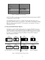
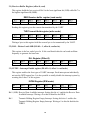
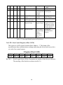
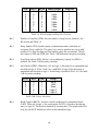
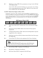
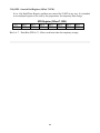
PC 31C 8 Port Serial Card User's Manual For the IBM PC, PC/XT, PC/AT, PS/2 386, 486, Pentium, ISA and EISA computers All rights reserved. No part of this Publication may be copied, stored in a retrieval system, or transmitted, in any form by any means, electronic, mechanical, by photocopying, recording, or otherwise, in whole or in part, without prior written permission from the Publishers. Third Edition 29 July 1996 July 1996 Printing Information furnished in this manual is believed to be accurate and reliable; however no responsibility is assumed for its use, nor for any infringements of patents or other rights of third parties which may result from its use. IBM, IBM PC/XT/AT and IBM PS/2 are trademarks of International Business Machine Corporation. MicroSoft and MSDOS are trademarks of MicroSoft Corporation. We acknowledge all other trademarks from companies mentioned in this User’s Manual. Copyright: S. Allie and Eagle Technology 2 Table of Contents Page Introduction Features PC 31 Package Typical Applications 5 5 5 5 Chapter 1: Installation 1.1) Setting the Base Address Table 1: Address for typical I/O addresses 1.2) Interrupt Jumper Settings Figure 3: Interrupt Jumper Settings Table 2: Standard Interrupt Settings 1.3) Interrupt Enable/Disable Jumpers Figure 3a: IRQ Enable/Disable Jumper Settings 1.4) Installing the PC 31B/C in your Computer 6 6 8 8 8 8 9 9 10 Chapter 2: Interconnections 2.0) Introduction 2.1) Connections to Backplane of PC 2.2) IDC 10 Male Connector Figure 4: PC 31 Interface IDE Connector 2.3) COM Port Arrangement Table 2.3a: COM Port Arrangement 2.4) DB9 / DB25 User Connector Figure 5: PC 31 DB9 / DB 25 Interface Connector 11 11 11 11 11 13 13 13 13 Chapter 3: Register Structure 3.0) Introduction Table 3.0: PC 31 Register Structure 3.1) RBR (Receiver Buffer) Register 3.2) DLL (Divisor Latch LSB) Register 3.3) INTEN (Interrupt Enable) Register 3.4) DLM (Divisor Latch MSB) Register 3.5) IIR (Interrupt Identification) Register Table 3.5: Interrupt ID bit definitions 3.6) LCR (Line Control) Register Table 3.6: Word Length and Stop Bit Selections Table 3.6b: Parity Selection 3.7) MCR (Modem Control) Register 3.8) LSR (Line Status) Register 3.9) MSR (Modem Status) Register 3.10) SPR (Scratch Pad) Register 15 15 15 16 16 16 17 17 17 18 19 19 20 21 22 23 3 Table of Contents Continued... Page Chapter 4: Driver Software 4.0) Introduction 4.1) PC76 Software Package 4.2) PC76MODE utility program 4.3) PC76DRVR DOS Device Driver 4.4) PC76TALK.COM Terminal program 4.5) PC76TEST.COM test program 24 24 24 25 26 27 27 Chapter 5: Testing the PC 31 Card 28 Chapter 6: Problem 1: Problem 2: Problem 3: Problem 4: Problem 5: Problem 6: 29 29 29 29 29 29 30 Troubleshooting the PC 31 Board does not respond Tx line does not transmit data Rx Line does not receive data correctly System hangs when PC 31 is plugged into computer COM Port 5 and 6 does not respond Under Windows NT, system boots but BUS mouse does not respond Problem 7: Under Windows NT, system crashes in middle of booting sequence 30 Chapter 7: Repair Service 31 Chapter 8: Specifications 32 Appendix A: Layout Diagram 33 4 Introduction The PC 31B/C 8 port serial card is an industrial interface card used to communicate with various devices asynchronously via the IBM PC/XT/AT. Each card provides eight standard RS232 interface ports spanning from COM1 thru to COM8. Each of the COM ports can be configured with its own unique interrupt line. The serial interface is implemented with a 16450 UART connected to associated drivers. The 16450 UART is a faster version of the 8250 formerly found on IBM XT models. The PC 31 fits into one of the IBM ISA expansion slots. Typical applications ¯ Controlling PLCs ¯ Laboratory Automation ¯ Data Logger via RS232 ¯ Product testing ¯ Energy management Features ¯ Controls up to 8 external devices per board ¯ Multiple boards are accommodated ¯ Interrupt selectable from IRQ 2, 3, 4, 5, 6, 7, 10, 11, 12, 15 ¯ Driver software in C plus demostration and test programs ¯ Commercial programs like Telix, Testpoint and DasyLab fully supports the PC 31. PC 31 Package The PC 31 package consists of: PC 31 Interface Card PC 31 User's Manual 8 cable connectors (IDC to DB25 / DB9) One 5.25' or 3.5' diskette containing the PC 31 drivers and demonstration software If any of the items is missing, contact your dealer immediately specifying which components are missing. 5 Chapter 1: Installation There are two aspects of the PC 31 that must be configured: 1.1) The Base Address This address determines where the board is accessed. This can be set by a 4-way DIP switch found on the PC 31 Board. The address range are 160h to 3F8h. The PC 31 serial port occupies a block of 8 consecutive I/O addresses. The base address setting controls where the block starts. This base address must be unique to the PC 31 only and no other card must occupy this address. If multiple PC 31 boards are installed in one computer then each board must have a different base address. The base address can be assigned to a range of addresses 160h to 3F8h in 8 byte boundaries. Table 1 shows the I/O addresses occupied by standard interface cards. Refer to the Base Address Setting Table in Appendix A for a list of the various base address settings that the PC 31 can occupy. The base address setting can be set by adjusting the 4-way dip switch on the PC 31. Offset addresses are fixed and mapped to certain locations. In other words, each serial port does not necessarily occupy an address offset from the base address. For example, the Port 1 base address is at 3F8 [ie: 3F8 to 3FFh] while Port 2 base address is at 2F8h. The reason for this is to enable the user to adjust the DIP SW in a certain way in order to map the ports to standard DOS Serial Ports. 6 Table 1: Addresses for standard I/O devices Address Standard device 000-1FF 200-20F 210-217 220-24F 250-257 258-25F 260-277 278-26F 280-2EF 2F0-2F7 2F8-2FF 300-31F 320-32F 330-377 378-37F 380-38F 390-39F 3A0-3AF 3B0-3BF 3C0-3CF 3D0-3DF 3E0-3E7 3E3-3EF 3F0-3F7 3F8-3FF 400-FFF Internal system board Games port Expansion unit Reserved Not assigned Intel 'Above Board' Not assigned reserved Not assigned LPT2 COM2 Prototype Board Hard Disk Not assigned LPT1 SDLC communications Not assigned Binary comms Mono Display Adaptor Reserved CGA Reserved Not assigned Floppy disk COM1 Not used see below Table 1: Standard I/O Addresses The PC 31 DIP SW is described in figure 1 below: ON 1 2 3 4 Figure 1: Dip Switch (4 not used) Care should be taken to ensure that the PC 31C I/O addresses is not being used by other devices in the PC. If your computer has boards not listed in Table 1 (such as IDE+I/O Card, LAN adaptors, back-up boards or other engineering boards), you should consult the User's Manual for these boards for information on the address ranges used. In most cases, base address of 2A0h (for the 1st Port) is a good choice. Address 2A0h is also the factory default base address setting. 7 SW1 SW2 SW3 PORT 1 ON ON ON ON ON OFF ON OFF ON ON OFF OFF OFF ON ON OFF ON OFF 3F83FF 160167 2A02A7 2F82FF 3F83FF 210217 PORT2 2F82FF 168168 2A82AF 2A82AF 2F82FF 21821F PORT 3 PORT 4 2B02B7 170177 2B02B7 2B02B7 3E83EF 220227 2B82BF 17817F 2B82BF 2B82BF 2E82EF 22822F PORT 5 1A01A7 180187 1A01A7 1A01A7 280287 230237 PORT 6 PORT 7 1A81AF 18818F 1A81AF 1A81AF 28828F 23823F 1B01B7 190197 1B01B7 1B01B7 290297 240247 PORT8 1B81BF 19819F 1B81BF 1B81BF 29829F 24824F Table 1.1: Base Address Switch Settings 1.2) Interrupt Jumper Settings Each COM port can control an interrupt level. To allow the PC 31 to send interrupts to the system, bit 3 of the Modem Control Register must be set high. Refer to figure 3 for the interrupt jumper settings. 2 4 6 10 12 2 4 6 10 12 2 4 6 10 12 2 4 6 10 12 3 5 7 11 15 3 5 7 11 15 3 5 7 11 15 3 5 7 11 15 IRQ 3 IRQ 4 IRQ 5 IRQ 2 2 4 6 10 12 2 4 6 10 12 2 4 6 10 12 2 4 6 10 12 3 5 7 11 15 3 5 7 11 15 3 5 7 11 15 3 5 7 11 15 IRQ 10 IRQ 11 IRQ 12 Figure 3: Interrupt jumper settings In a standard PC, the interrupt levels are allocated as follows: 8 IRQ15 Level Level IRQ0 IRQ1 IRQ2/IRQ9 IRQ3 IRQ4 IRQ5 IRQ6 IRQ7 Allocation System timer Keyboard Display Adaptor COM1 (if installed) COM2 (if installed) LPT2 (if installed) Floppy disk controller LPT1 (if installed) Table 2: Standard interrupt settings On PC ATs, IRQ2 is used by the system board itself and any interrupt requests on IRQ2 is transparently re-routed to IRQ9. The default IRQ setting on the PC 31 is IRQ4. Note that unless the interrupt line is specifically enabled by software (by setting bit 3 of the Modem Control Register [MCR] high), the interrupt output from the PC 31 is tri-stated (ie: not connected). It is also tristated upon power-up. 1.3) Interrupt Enable/Disable Jumpers The IRQ line on the PC 31B/C Board are driven low using the 220R SIP. Certain non compatible computer cards does not like this type of configuration. Provision was hence made to disconnect the unused IRQ lines from the ISA BUS completely. By removing the jumper, you automatically disconnect the IRQ line from the BUS. Examples of jumper settings are as follows: LK1 IRQ EN/DIS LK2 IRQ EN/DIS I2 I3 I4 I5 I6 I7 I10 I11 I12 I15 IRQ 2 ENABLED IRQ 11 ENABLED LK1 IRQ EN/DIS I2 I3 I4 I5 I6 I7 IRQ 2,3,4,7 ENABLED LK1 IRQ EN/DIS LK2 IRQ EN/DIS LK1 IRQ EN/DIS I2 I3 I4 I5 I6 I7 I10 I11 I12 I15 I2 I3 I4 I5 I6 I7 IRQ 2,3,7 ENABLED ALL IRQs DISABLED ALL IRQs DISABLED Figure 3a: IRQ Enable/Disable Jumper Settings 9 LK2 IRQ EN/DIS I10 I11 I12 I15 IRQ 10,11,15 ENABLED LK2 IRQ EN/DIS I10 I11 I12 I15 IRQ 10,15 ENABLED + Note You must first enable the IRQ line using the above jumpers before setting the IRQ line (JP1 to JP8) of the COMs Ports. COM port failure will result if the IRQ line is not enabled via LK2 or LK1. 1.4) Installation Requirements: ¯ XT/286/386/486 Computer ¯ Phillips Screw Driver (or one to match screw on the computer cabinet and bracket) ¯ 8 bit or 16 bit bus slot Procedure: a) Switch off the computer and all attached devices b) Unplug power cord from the computer and all attached devices. + Warning Failure to disconnect all power cables can result in hazardous conditions, as there may be dangerous voltage levels present in externally connected cables. c) Remove the top cover from the PC. If you are not sure how to do this, consult the manual supplied with the system unit. d) Choose any 8 or 16 bit expansion slot and remove the screw from the metal bracket fixed corresponding to the chosen slot. e) Align the gold plated edge connector with the edge socket and the rear adaptor slot with the board bracket. Firmly press the board down into the socket on the computer's system board. Ensure that the board's edge connector is in the socket and has not slipped sideways past the socket. f) Replace the screw on the bracket and tighten the screw to the back panel. g) Replace the computer's cover. Plug in all cables and switch the computer power on. The PC 31 is now installed. 10 CHAPTER 2: Interconnections 2.0) Introduction The PC 31 Eight Port Serial Card plugs into any ISA expansion slot at the gold finger edge connectors J1/J2 and J4. The board communicates to the user circuit via a connector mounted on the PCB. An IDE female header with ribbon cable maps to a DB9 Male of DB25 Female Connector. This chapter describes these connectors 2.1) Connections to the IBM Bus The PC 31 board may be plugged into any slot of the computer backplane with the exception of J8 slot of the IBM XTs. All data transfers to and from the host computer is channelled via this connector. 2.2) IDC 10 Male Header The PC 31 interfaces to the external world via a 10 way IDC male connector (header) that maps signals to a 9 way or 25 way D-type male connector. This connector accommodates the following signals: ¯ RX and TX lines ¯ RTS, CTS lines ¯ DSR, DCD, DTR and RI lines ¯ GND line Figure 4: PC 31 Interface Connector (as seen from the rear of the PC) 11 Figure 4 graphically shows the male header on the PC 31 together with their pin assignments. Note that the pin connections refer to the pin numbers of the connector when looking into the connector from the component side of the PC 31. Note that cables that fits onto this male header are provided and maps to a DB 9 or DB 25. These are discussed in section 2.3. 12 2.3) COM Port Arrangement The COM ports are arranged in the following order (on REV 1C Boards): HEADER NO H1 H2 H3 H4 H5 H6 H7 H8 INTERRUPT JUMPER HEADER JP1 JP2 JP3 JP4 JP5 JP6 JP7 JP8 COM PORT ARRANGEMENT COM PORT 1 COM PORT 2 COM PORT 3 COM PORT 4 COM PORT 6 COM PORT 5 COM PORT 7 COM PORT 8 Table 2.3a: COM Port Arrangement + Note Some of the COM ports and associated headers (incremental) are not in sequence. Ensure that you follow the above table at all times. Also check if the PC 31B/C you have is marked REV 1C. The template is given in the layout diagram section. 2.4) User Connector The PC 31 interfaces to the external world via a 10 way IDC connector that maps signals to a 9 way or 25 way D-type male connector. Figure 5: PC 31 Interface Connector (as seen from the rear of the PC) 13 Figure 5 graphically shows the connector together with their pin assignments. Note that the pin connections refer to the pin numbers of the connector when looking into the connector from the rear of the computer. Also note that the pin numbers are embossed on the connector itself. 14 CHAPTER 3: Register Structure 3.0) Introduction At the lowest level, the PC 31 can be programmed using I/O input and output instructions. This chapter contains the information on all the PC 31 registers. Although programming the board is not difficult, it is time consuming and requires detailed knowledge of the PC 31 as well as the operation of the host PC and its operating system. In order to simplify the process, a set of driver libraries is provided. The use of these libraries allow access to all the board's functions and is described in Chapter 5: Programming guide. The serial port on the PC 31 occupies 4 consecutive addresses in the computer's I/O space. The layout of these registers are shown in Table 4: PC 31 COM Port register structure. The offset of the registers are given as offset addresses from the base address of the board. This base address is set with the Dip Switch as detailed in Chapter 2: Installation. Offset 0 DLAB 0 Read / Write 0 1 1 0 1 1 2 x 3 x 4 x 5 x 6 x Divisor latch LSB (DLL) Interrupt Enable Reg (IER) Divisor latch MSB (DLH) Interrupt ID register (IIR) Line Control Register (LCR) Modem control register (MCR) Line Status Register (LSR) Modem Status Register (MSR) Read Rx buffer register (RBR) Table 3.0: PC 31 register structure 15 Write Transmit Holding register (THR) 3.1) Receiver Buffer Register (offset 0, read) This register holds the byte received. Bit 0 is the least significant bit (LSB) while Bit 7 is the highest significant bit (MSB). RBR Receiver buffer register (read mode) Bit 7 XD7 Bit 6 XD6 Bit 5 XD5 Bit 4 XD4 Bit 3 XD3 Bit 2 XD2 Bit 1 XD1 Bit 0 XD0 Reading this register gives the current data translated by the UART. THR Transmit Hold register (write mode) Bit 7 XD7 Bit 6 XD6 Bit 5 XD5 Bit 4 XD4 Bit 3 XD3 Bit 2 XD2 Bit 1 XD1 Bit 0 XD0 Writing a byte to this register hold the current byte to be transmitted by the UART. 3.2) DLL - Divisor Latch LSB (DLAB = 1, offset 0, read/write) This register is the low order byte of a 16 bit word that divides the on board oscillator frequency to generate the baud rate. DLL Register (Offset 0) Bit 7 D7 Bit 6 D6 Bit 5 D5 Bit 4 D4 Bit 3 D3 Bit 2 D2 Bit 1 D1 Bit 0 D0 3.3) INTEN - Interrupt Enable register (DLAB = 0, offset 1: read/write) This register enables the four types of UART interrupts. Each interrupt can individually activate the INTR output line. It is also possible to totally disable the interrupt system by resetting bits 0 thru 3 of this register. INTEN Register (R/W mode) Bit 7 0 Bit 6 0 Bit 5 0 Bit 4 0 Bit 3 MSI Bit 2 RLSI Bit 1 THREI Bit 0 RDAI Bit 0 (LSB): Receive Data Available interrupt: Setting this bit to 1 enables the Receive Data Available Interrupt. Writing a 0 to this bit disables the RDAI. Bit 1 Transmit Holding Register Empty Interrupt: Setting this bit to 1 enables the Transmit Holding Register Empty Interrupt. Writing a 0 to this bit disables the THREI. 16 Bit 2 Receive Line Status Interrupt: Setting this bit to 1 enables interrupt on overrun, parity, framing errors and break indication. Writing a 0 to this bit disables the RLSI. Bit 3 MODEM Status Interrupt: Setting this bit to 1 enables interrupt on clear to send, data set ready, ring indicator and carrier detect. Writing a 0 to this bit disables the MSI. Bits 4 to 7: These bits are set to Logic 0. Reading these bits will yield all zeros. 3.4) DLM - Divisor Latch MSB (DLAB = 1, offset 1, read/write) This register is the high order byte of a 16 bit word that divides the on board oscillator frequency to generate the baud rate. DLM Register (Offset 1) Bit 7 D7 Bit 6 D6 Bit 5 D5 Bit 4 D4 Bit 3 D3 Bit 2 D2 Bit 1 D1 Bit 0 D0 3.5) IIR - Interrupt Identification Register (Offset 2, R/W) To minimize software overhead during data character transfer, the UART prioritizes interrupts into four levels and records these in the IIR. II Register (Offset 2, R/W) Bit 7 FFE Bit 6 FFE Bit 5 0 Bit 4 0 Bit 3 IID2 Bit 2 IID1 Bit 1 IID0 Bit 0 IP Bit 0: Interrupt Pending. When logic 0, it indicates an interrupt is pending and the contents of the interrupt ID register may be used to determines the interrupt source (See Table 3.5). Bits 1-3: These bits indicates highest priority interrupt pending if any. See table 3.5. Note that IID2 is always 0 in character mode. 17 IID2 IID1 IID2 IP Priority Interrupt Type Interrupt Source Interrupt RES CNTRL x 0 x 1 x 1 1 0 N/A Highest None Receiver Line Status N/A Reading the line status register 0 1 0 0 Second 1 1 0 0 Second 0 0 1 0 Third Received Data Ready Character Timeout (FIFO mode only) Transmitter Holding Register Empty None Overrurn, parity or Framing Error or Break Interrupt Receiver Data Available 0 0 0 0 Fourth MODEM Status Reading the Receiver Buffer Register Transmit holding Reading the IIR Register Empty Register (if source of interrupt) or writing into the Transmitter Holding Register. Clear to Send, Reading the Data Set Ready MODEM Status or Ring Register Indicator or Data Carrier Detect. Table 3.5: Interrupt Identification Bit Definitions 3.6) LCR - Line Control Register (Offset 3, R/W) This register is a R/W register located at Base Address + 3. The format of the asynchrounous data communications exchange and setting the divisor latch access bit is set via the Line control register. II Register (Offset 2, R/W) Bit 7 DLAB Bit 0 & 1: Bit 6 Bit 5 BRCTL STKP Bit 4 EPS Bit 3 PEN Bit 2 STB Bit 1 WLSH Bit 0 WLSL Word Length Select (WLSx): Determines the number of data bits per character. The encoding of the data bits are shown in table 3.6. 18 STB 0 0 0 0 1 1 1 1 WLS1 0 0 1 1 0 0 1 1 WLS0 0 1 0 1 0 1 0 1 Word Length 5 bits 6 bits 7 bits 8 bits 5 bits 6 bits 7 bits 8 bits Stop bits 1 1 1 1 1.5 2 2 2 Table 3.6: Word Length and Stop bit selections Bit 2: Number of Stop Bits (STB): Sets the number of stop bits per character. See WLSx bits and Table 3.6. Bit 3: Parity Enable (PEN): Enables parity on transmission and verification on reception. Parity enable bit The parity bit is used to produce an even or odd number of 1s when the data word bits and the parity bit are summed. This bit also relates to EPS and STPK bits. Table 3.6B determines the parity encoding. Bit 4: Even Parity Select (EPS): Selects even or odd parity if parity bit (PEN) is enabled. See Table 3.6B for parity encoding. Bit 5: Stick Parity (STKP): When bits 3,4,5 are logic 1, the parity bit is transmitted and checked as logic 0. If bits 3 and 5 are 1 and Bit 4 is logic 0 then the parity is transmitted and checked as logic 1. Stick Parity is disabled if bit 5 is 0. See table 3.6B for parity encoding. STKP x 0 0 1 1 EPS x 0 1 0 1 PEN 0 1 1 1 1 Parity None Odd Even Logic 1 Logic 0 Table 3.6B: Parity selections Bit 6: Break Control (BKCN): It causes a break condition to be transmitted bythe UART. When set to logic 1, the serial output (SOUT) is forced to the spacing state (ie: logic 0). The break is disabled by resetting bit 6. The break control bit only acts on SOUT and has no effect on the transmitter logic. 19 Bit 7: Divisor latch Access Bit (DLAB): It must be set high to access the Divisor Latches of the Baud Rate Generator during Read / Write. Setting this bit to 0 allows access to the Receiver Buffer, Transmit Holding Register or the interrupt Enable Register (see table 4). 3.7) MCR - Modem Control Register (Offset 4, R/W) This register R/W controls the interface with the MODEM or data set. MCR Register (Offset 4, R/W) Bit 7 0 Bit 6 0 Bit 5 0 Bit 4 LOOP Bit 3 OUT2 Bit 2 OUT1 Bit 1 RTS Bit 0 DTR Bit 0: Data Terminal Ready (DTR): This bit is used for output driver control. When this bit is set to logic 1, the /DTR line (ie: on the DB9 connector) is forced to a logic 0. Bit 1: Request To Send (RTS): This bit controls the Request to Send line. It affects the /RTS line in the same manner as bit 0. Bit 2: Output 1 (OUT1): This bit controls the Output 1 line which is an auxilliary user output. It effect the /OUT 1 line in the same manner as bit 0. Bit 3: Output 2 (/OUT2): This bit controls the Output 2 line which is an auxilliary user output. It affects the /OUT 2 line in the same manner as bit 0. Bit 4: Loopback Enable (LOOP): This bit provides a local loopback feature for diagnostic testing of the UART. When bit 4 is set high, the transmitter shift register is internally connected to the receiver shift register, the four MODEM control inputs (/DSR, /CTS, /RI and /DCD) are disconnected and the four MODEM control outputs are internally connected to the four MODEM control inputs. The MODEM control output pins are forced to their inactive state (high). In a loopback mode, the data transmitted is received immediately. This allows the CPU to verify the transmitted and received data paths of the UART. The transmitter and receiver interrupts are fully operational. The MODEM Control Interrupts are also operational but the interrupt sources are now the lower four bits of the MODEM Control Register instead of the four MODEM Control Inputs. The Interrupts are still controlled by the Interrupt Enable Register. Bit 5 to 7: These bits are permanently set to logic 0. 20 3.8) LSR - Line Status Register (Offset 5, R/W) It provides status information to the CPU concerning data transfer. LSR Register (Offset 5, R/W) Bit 7 FFRX Bit 6 TEMT Bit 5 THRE Bit 4 BI Bit 3 FE Bit 2 PE Bit 1 OE Bit 0 DR Bit 0: Data Ready (DR): Bit is set to logic 1 it whenever a complete incoming character has been received and transferred into the Receiver Buffer Register. This bit is reset by reading the data in the Receiver Buffer Register. Bit 1: Overrrun Error (OE): Indicates that the Receiver Buffer was not read before the next character was transferred into the Receiver Buffer Register thereby destroying the previous character. Bit 2: Parity Error (PE): Indicates that the received data character does not have the correct even or odd parity, as selected by the even parity select bit. The PE bit is set to logic 1 upon detection of a parity error and is reset to logic 0 whenever the CPU readds the content of the Line Status Register. Bit 3: Framing Error (FE): Indicates that the received character has an invalid stop bit. Bit 3 is set to logic 1 whenever the Stop bit following the last data bit or parity bit is a logic 0 (Spacing level). Bit 4: Break Interrupt (BI): Bit 4 is set to 1 whenever the received data input is held in the Spacing state (logic 0) for longer than the full word transmission time ( ie: the total time of Start bit + data bits + parity + Stop bits). This BI bit is reset whenever the CPU reads the contents of the Line Status Register. Bit 5: Tranmitter Holding Register Empty (TMRE): This bit indicates that the UART isready to accept a new for transmission. It also causes the UART to issue an interrupt to the CPU when the Transmit Holding Register Empty Interrupt Enable is set high.The THRE bit is set to 1 when a character is transferred from the Transmitter Holding Register into the Transmitter Shift Register. The bit is reset to logic 0 when writing to the Transmitter Holding Register. Bit 6: Transmitter Empty indicator (TEMT): This bit is set to 1 whenever the Transmitter Holding Register (THR) or the Transmitter Shift Register (TSR) are both empty. TEMT is reset by writing a character to the Transmitter Holding Register. 21 Bit 7: FIFO Receiver Error (FFRX): Bit is permanently set to logic 0 in the 16450 and 16550 character mode. In the 16C550, FIFO mode, this bit indicates one or more parity errors, framing errors or break indications in the receiver FIFO. FFRX bit is reset when a read cycle is initiated on the Line Status Register. 3.9) MSR - Modem Status Register (Offset 6, R/W) Provides the current state of the control line from the MODEM (or peripheral device) to the CPU. In addition to current state information, four bits of the MODEM Status Register provide change information. This bits are set whenever a control input from the MODEM changes state. These bits are reset upon initiation of a CPU read cycle to the MODEM Status Register. MSR Register (Offset 6, R/W) Bit 7 DCD Bit 6 RI Bit 5 DSR Bit 4 CTS Bit 3 DDCD Bit 2 TERI Bit 1 DDSR Bit 0 DCTS Bit 0: Delta Clear to Send: (DCTS): Indicates that a Clear to Send input has changd state. Bit 1: Delta Data Set Ready (DDSR): Indicates that a Data Set Ready input has changed state. Bit 2: Trailing Edge Ring Indicator (TERI): Indicates that the Ring Indicator input has changed from a low to a high state. Bit 3: Delta Data Carrier Detect (DDCD): Indicates that the Data Carrier Detect input has changed state. Bit 4: Clear to Send (CTS): This bit is the complement of the Clear to Send input. + Note Bits DDCD, TERI, DDSR and DCTS are the sources of the Modem status interrupts. These bits are reset when the Modem Status Register is read. Bit 5: Data Set Ready (DSR): Complement of the DSR input. Bit 6: Ring Indicator: Complement of the RI input. Bit 7: Data Carrier Detect (DCD): Complement of the DCD input. 22 3.10) SPR - Scratch Pad Register (Offset 7, R/W) It is a 8 bit Read/Write Register and does not control the UART in any way. It is intended as a scratchpad register to be used by the programmer for temporary data storage. SPR Register (Offset 7, R/W) Bit 7 XD7 Bit 6 XD6 Bit 5 XD5 Bit 4 XD4 Bit 3 XD3 Bit 2 XD2 Bit 1 XD1 Bit 0 XD0 Bits 0 to 7: Data Bits (XD0 to 7): Allows read/write data for temporary storage. 23 Chapter 4: Driver Software 4.0) Introduction Full driver software is supplied with the PC 31 package. It contains full source code, utility programs and a terminal program. Note that you do not need to use the driver library. Most commercial communications programs like Telix, Crosstalk, COMBIOS, etc supports the PC 31C. All that is required in these packages is the I/O base address of the COM port and the Interrupt Request Line (IRQ) used. Third Party Driver libraries can also be used with the PC 31C. Commercial packages like Testpoint, DasyLab, etc has a RS232 Driver libraries available. This can be used without any problems. 4.1) The PC 76 Software Package This package provides an introduction to the PC 31C and includes source code so that the files may altered to suite user applications. Quick reference is given below: Program name PC76READ.ME PC76MODE.EXE PC76MODE.C PC76DRVR.SYS PC76DRVR.ASM PC76TALK.ASM PC76TALK.COM PC76TEST.EXE PC76TEST.C Description Text file that describes the PC 76 software package Utility program that configuresthe PC 31’s eight COM ports C source code for the above utility program DOS Device driver that control the PC 31’s COM ports Source code for the above device driver Assembly source code for PC76TALK.COM terminal program Simple terminal program Test program that checks the PC 31 COM ports C source code for the above test program See the PC76READ.ME manual for detailed documentation on the PC 76. 24 4.2) PC76MODE utility program This program allows the user to configure the operational parameters for any of the eight RS232 ports on the PC 31. The parameters that may be configured are: Baud Rate: Parity: No of data bits/character: No of stop bits/character: 110, 150, 300, 600, 1200, 2400, 4800, 9600, 19200 Odd, Even or none 7 or 8 1 or 2 Each port is referred to as COMn where n = 1...8, For example, to configure COM5 to 9600 baud, 8 data bits, one stop bit and no parity, type the following on the system prompt: C:>pc76mode com5:9600,n,8,1 PC76MODE wll either return and re-display the configuration, or return an error message. The COM port and the baud rate must be specified. Parity, the number of data bits and defaults for data and stop bits are 7 and 1 respectively. However, at 110 baud, the stop bit default to 2. The general form of the PC76MODE command is: PCMODE device:baud [,parity][,databits][,stopbits] where: Device is COM1, COM2......COM8 Baud is 110, 150, 300, 600, 1200, 2400, 4800, 9600, 19200 Parity is n, o, e Databits are 7 or 8 Stopbits are 1 or 2 [ ] indicates that it is an optional configuration + Warning PC76MODE cannot be used to redirect devices as the standard DOS MODE command does. Nor does it support the MODE command's 'P' option, where COM1..COM8 devices permanently retry input or output characters (see PC76DRVR). 25 PCMODE assumes that the PC 31's I/O addresses are as follows: COM1: COM2: COM3: COM4: COM5: COM6: COM7: COM8: 3F8h 2F8h 3E8h 2E8h 280h 288h 290h 298h DIP SW Settings (S1) for the above configuration are: SW3 (ON). SW1 (OFF), SW2 (ON), The PC76MODE commands can be placed in your AUTOEXEC.BAT file which allows automatic setup of the COM ports during bootup. + Note Under Windows V3.1, WIN 95 or Windows NT, you cannot use the above program to initialize the COM ports. Use the Control Panel / Ports option to configure the COM ports correctly. 4.3) The PC76DRVR.SYS Device Driver The PC76DRVR.SYS contains the example device driver for the eight RS232 ports on the PC 31. It allows the ports to be used in a similiar way files named COM1: to COM8:. For example, to transmit the PC76READ.ME file from the RS232 port COM5, you must type: copy PC76READ.ME > COM5 PC76DRVR also allows programmers to refer to the ports by their logical names in programs. To install PC76DRVR, enter the follow line into CONFIG.SYS DEVICE=PC76DRVR.SYS 26 Also ensure that you place the driver in the root directory (ie: C:\ ). PC76DRVR will be installed when the system is rebooted. During booting the following message should be displayed on the computer screen: PC 76 drivers (v1.1) for COM1: to COM8: installed Before accessing the serial devices, ensure that you configure the baud rate, etc with the utility program PC76MODE.EXE. PC76DRVR assumes that the PC 31’s I/O addresses are as shown for PC76MODE. It performs permanent retries on COM1....COM8: to either input or output characters. It will hang if the output is stopped on output or if no input characters are available during input. + Note The PC76DRVR does not support IOCTL calls, although the entry points to the various functions are provided in the source code (PC76DRVR.ASM). 4.4) The PC76TALK.COM Terminal Program PCTALK.COM is a simple terminal emulator which is included as an example of using interrupts with the COM ports. As supplied, it will operate in full duplex via COM1:, emulating a subset ofthe Televideo 950 control codes. It uses IRQ 4 (default) and must be selected by jumper on the PC 31 before the emulator is run. Baud rate, parity, data and stop bits must be set up using PC76MODE before running the terminal program. Note that PC76TALK.COM does not use the PC76DRVR device driver. To exit from PC76TALK, use any special function key, such as F1. The program explains how to modify the program to run in half duplex; use different IRQs, and use other COM: channels. 4.5) The PC76TEST.COM PC76TEST.COM is a very simple terminal emulator written in C, which can be configured to communicate with any of the PC 31 COM ports. This program is provided to allow users to test simple serial I/O via any serial ports. It also gives an example of how to write your own C-based comms applications without the need to use an Assembler. 27 Chapter 5: Testing the PC 31 Before attempting to interface the PC 31 with your application, it is essential that you test the board first. This is done using the following Procedure: Install the PC 31 using the procedure described in the Chapter 2: Installation. Proceed as follows: ¯ Switch the Computer on ¯ On the DOS prompt, run the program: PC76TEST.COM. The program will display instructions: -------------------- PC 31TEST --------------------(Talk to ANY 8250 serial channel at any addresss) N = Set COM Address T = Talk via efault base address ^C = Exit If you want to test a serial port at a different base address then select N on the program menu and enter the base address or COM port (1 to 8). To test the COM port type T. If any error messages are displayed then the PC 31 was not installed at that address. Try a different base address (eg: 2F8h) and re-run the test S/W. If the problem persists then try changing the IRQ line as specified in Chapter 2 and rerun test software. The board should work. You can also use other commercially available utilities like QAPLUStm from Diagsoft or CHECKITtm. These utilities test the serial ports internal registers, internal loopback data as well as external loopback data at specific Baud rates. 28 Chapter 6: Troubleshooting Problem: The PC 31 board does not respond at specified base address. Solution: Another I/O card might be using the same base address location as the PC 31. The most common card that can cause conflicts is your IDE+I/O card. This card contains two serial port (ie: COM1 and COM2) that will interfere with the PC31’s operation. Disable the COM ports and rerun test software. If the problem persists then try changing the IRQ of the serial port and rerun test software (or commercial COMs software like TELIX, COMBIOS, etc). The PC 31 should work. If the test still fails then the PC 31 is faulty. Return the board to your distributor for repairs. Problem: Solution: Problem: Tx line does not transmit data at all. Try a different COM port on the PC 31 Card. If the Tx line on this COM port is fully operation then it is possible that the Line driver on the PC 31 is faulty. Return to your distributor for repairs. Rx line does not respond at all. Solution: Try a different COM port on the PC 31 Card. If the Tx line on this COM port is fully operation then it is possible that the Line driver on the PC 31 is faulty. Return to your distributor for repairs. Problem: System hangs when PC 31 is placed in the computer. Solution: It could be as a result of another Card conflicting with the PC 31’s I/O Base Addresses. Try a base different address. If it still fails then the PC 31 is faulty, return to your distributor for repairs. Problem: COM Port at Header H5 and Header H6 are not responding during setup. Solution: The User probably assumed that Header H5 is COM Port 5 and Header H6 is COM port 6. This is NOT correct. COM port 5 header number is H6 with IRQ Jumper JP5 and COM port 6 Header is H5 with IRQ Jumper JP6. 29 Problem: Under Windows NT or Windows 95, the system boots up correctly but the BUS Mouse (NOT serial mouse) does not work. Solution: The BUS mouse uses IRQ 12. If this IRQ line is enabled on the PC 31 (via LK2) and the COM port Jumper (any of JP1 thru JP8) then the Mouse will fail to operate. The BUS mouse also uses IRQ 12 hence you must not use this IRQ line for the COM ports. I suggest you disable the IRQ 12 line completely using the LK2 Jumper. In other words remove the Jumper under I12 on LK2. Your system should operate normally. Problem: Under Windows 95 or NT, the system boots up but crashes in the middle of the booting process. Solution: It could be as result of an I/O base address conflict with the PC 31 Board and your network Card. I suggest that you check your network card’s base address. If it overlaps with the PC 31, the system will crash. The solution would be to change the base address of the Network Card. + Warning Any parts replaced on the PC 31 must be done by a qualified or trained technician. If you (the user) is not a trained technician then rather return the board to your distributor for repairs explaining in detail what the problem is. If you cannot solve the problem then simply call your distributor for immediate help. 30 Chapter 7: Repair Service The PC 31 is guaranteed for a period of 1 year. If the board is faulty within this period, we will gladly repair it free of charge provided that the maximum specifications was not exceeded. If any burn't tracks are seen on the PC 31 Board, warranty will be void. A repair charge will be levied in the user requires the board to be repaired Before sending the board to your distributor for repairs, ensure that you go through Chapter 6 TroubleShooting Hints thoroughly. If after you have gone through this Chapter, the board still does not work, return it for repairs stating in detail what the problem is. Our repair service centre will be available to repair our products even after the 1 year warranty. A small service fee will be levied which usually covers the cost of the components that are faulty. 31 Chapter 8: PC 31 Specifications Computer Host Interface Base Address: Switchable from 0160h to 03f8h in fixed locations Bus Type: XT, AT, ISA or EISA Number of Registers: Eight 8-bit Interrupts: Jumper selectable from IRQ 2 - IRQ7; IRQ 10 - IRQ 15 Power Requirements: +5V DC at ±800mA Max UART and External Interface Number of UART Ports: 8 Controllers used: 16C450 Asynchronous Communication ICs Transmit Drivers: 1488 or compatible (RS232) Receive Buffers: 1489 or compatible (RS232) Oscillator Frequency: 1.8432MHz Baud Rate: Programmable from 50 to 19.2k Data Bits: 5, 6, 7, or 8 Stop Bits: 1, 1.5 or 2 Parity Bits: Odd, even or none I/O connector: DB 9 or or DB 25 male connectors Enviromental and Physical Operating temperature: Storage temperature: Relative humidity: Board size: 0°C to 55°C -55°C to 150°C 5% to 90% non-condensing 170mm x 106mm Power Requirements +5V: +5V DC at ±800mA Max 32 APPENDIX A Layout Diagram 33


![LS5105 Document No 4 [PDF 493KB]](http://vs1.manualzilla.com/store/data/005800437_1-91570bc2ebb104ae0a2a4b7bb76bd213-150x150.png)