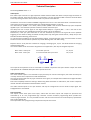
1
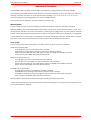
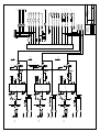
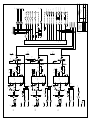
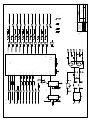
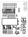
CDC‐3062 Instruction Book
Revision 15
I R T Electronics Pty Ltd A.B.N. 35 000 832 575
26 Hotham Parade, ARTARMON N.S.W. 2064 AUSTRALIA
National: Phone: (02) 9439 3744
Fax: (02) 9439 7439
International:
+61 2 9439 3744
+61 2 9439 7439
Email: [email protected]
Web: www.irtelectronics.com
IRT Eurocard
Type CDC‐3062
Priority Controller
Designed and manufactured in Australia
IRT can be found on the Internet at:
http://www.irtelectronics.com
www.irtelectronics.com
Page 1 of 18
3062‐CDC_ib_Rev15.doc
CDC‐3062 Instruction Book
Revision 15
IRT Eurocard
Type CDC‐3062
Priority Controller
Revision History
Revision
13
14
15
Date
24/09/2002
02/05/2008
25/06/2010
www.irtelectronics.com
By
AL
AL
AL
Change Description
Handbook mistakes updated as per ECR No. 1387.
Rear assembly updated for 4000 series frame.
PL3 connections corrected. Swapped 1A & 1B;
3A & 3B; and 5A & 5B.
Page 2 of 18
Applicable to:
S/N > 9704001
S/N > 9704001
S/N > 9704001
3062‐CDC_ib_Rev15.doc
CDC‐3062 Instruction Book
Revision 15
IRT Eurocard
Type CDC‐3062
Priority Controller
Instruction Book
Table of Contents
Section
Page
Revision History
Operational Safety
General Description
Operational Description
Technical Specifications
Technical Description
Internal Adjustments
Configuration
Link settings
Audio only operation
Installation
Operational Safety
Pre‐installation
Installation in frame or chassis
Connections
Front & rear panel connector diagrams
Maintenance & Storage
Warranty & Service
Equipment return
Drawing List Index
2
3
4
5
7
8
9
10
10
11
12
12
12
13
13
16
17
17
17
18
This instruction book applies to units later than S/N 9704001.
Operational Safety:
WARNING
Operation of electronic equipment involves the use of voltages and currents that
may be dangerous to human life. Note that under certain conditions dangerous
potentials may exist in some circuits when power controls are in the OFF position.
Maintenance personnel should observe all safety regulations.
Do not make any adjustments inside equipment with power ON unless proper
precautions are observed. All internal adjustments should only be made by suitably
qualified personnel. All operational adjustments are available externally without
the need for removing covers or use of extender cards.
www.irtelectronics.com
Page 3 of 18
3062‐CDC_ib_Rev15.doc
CDC‐3062 Instruction Book
Revision 15
IRT Eurocard
Type CDC‐3062
Priority Controller
General Description
The CDC‐3062 is a video presence detector that also provides logic and switching control circuitry for interfacing to
IRT 700, 3000 & 4000 series video and audio switchers. The main use for the controller is to provide control of
CDC-3062 Video Switching Logic Controller
Main
Video Input
Loop output
Video
Detector
OR
Remote,
Alarms
&
Status
Audio override
Front Panel Controls
Main
Reserve
Priority
Switch Logic
Controller
Standby
Local
3000 Series
Switcher Interface
Reserve
Video Input
Loop output
Alarm /
Switcher
Drivers
700 Series
Switcher
Control
Outputs
Manual / Auto
Video
Detector
OR
Video
Detector
OR
Auto /Manual
Auto Tally
Main OK
Reserve OK
Standby OK
Main Priority
Reserve
Priority
Standby
Priority
Main Tally
Reserve Tally
Standby Tally
Main Ctrl
Reserve Ctrl
Standby Ctrl
Local Ctrl
Audio override
Standby
Video Input
Loop output
Audio override
transmission link paths and to provide alarm and status information to centralised monitoring facilities.
The following features are provided:
• Automatic operation.
• Selection of main / reserve / standby priority.
• Local / remote control of all functions.
• Remote and local status information.
• Audio fail override facility using IRT AG‐738 / AAD‐4130 audio detector.
The video signals of the main, reserve and standby paths are monitored, with an indication provided to show the
loss of the input signal. Any of the main, reserve or standby paths can be selected as the priority path and,
provided a signal is present, this selection will be the ON AIR source.
If the priority selected path should fail the unit will provide control signals to select another input. Where a failure
occurs on main, reserve and standby inputs then the system will select the local input. Once any input signal is
restored, the system will switch back from the local signal to an input signal, with the priority‐selected input
having precedence when more than one input signal is available.
The front panel indicators and controls provided are:
• Fail LED's on the main, reserve and standby paths.
• Indication of the priority source selected.
• Indication of the ON AIR source.
• Auto/manual enable indication.
• Push buttons for priority selection of sources in auto mode and direct selection of manual mode.
www.irtelectronics.com
Page 4 of 18
3062‐CDC_ib_Rev15.doc
CDC‐3062 Instruction Book
Revision 15
Operational Description
The CDC‐3062 Eurocard module has three video failure detectors; designated main, reserve and standby.
Full interfacing to IRT 3000 series Eurocard switchers is provided, in addition it also has four logic level outputs for
selecting one of four crosspoints on an IRT Eurocard series switcher. (Types VA‐710, AA‐720 and / or AA‐751 (obsolete))
The four crosspoints may be designated main, reserve, standby and local.
The controller may be operated in one of two modes; manual or auto.
Manual mode:
In manual mode, the four front panel switches provide direct selection of the four controlled crosspoints.
Switching between auto and manual modes may be made using the front panel pushbutton switch or by an opto‐
isolated remote interface. The action of this switch / remote input is a toggle action and it is therefore essential
that this switch be returned to the auto position once any servicing work requiring manual operation is completed.
A visual indication of manual mode is provided by the red LED immediately below the manual switch. A remote
tally of this mode is also provided so that the mode is known when operated by remote control.
Auto mode:
In auto mode, the four front panel switches are used to set the “priority” of the four crosspoints.
If main has the priority then:
If a valid signal is present on main then main is selected.
If main fails and a valid signal is present on reserve then reserve is selected.
If main and reserve both fail and a valid signal is present on standby then standby is selected.
If main, reserve and standby all fail then local is selected.
If reserve has the priority then:
If a valid signal is present on reserve then reserve is selected.
If reserve fails and a valid signal is present on main then main is selected.
If main and reserve both fail and a valid signal is present on standby then standby is selected.
If main, reserve and standby all fail then local is selected.
If standby has the priority then:
If a valid signal is present on standby then standby is selected.
If standby fails and a valid signal is present on main then main is selected.
If standby and main both fail and a valid signal is present on reserve then reserve is selected.
If main, reserve and standby all fail then local is selected.
If a failed signal is restored then selection takes place according to the above priorities.
A video failure is deemed to have occurred when the synchronising signals of a composite video signal fall in level
by more than 6 dB from standard.
www.irtelectronics.com
Page 5 of 18
3062‐CDC_ib_Rev15.doc
CDC‐3062 Instruction Book
Revision 15
Front panel controls & indicators:
Pushbuttons:
The front panel has four selector pushbuttons called main, reserve, standby and local.
In manual, these are used to select crosspoints 1, 2, 3 & 4 of the connected video switcher.
In auto
main sets main as the priority channel
reserve sets reserve as the priority channel.
standby sets standby as the priority channel.
Each switch has an LED indicator.
In manual mode, the LED’s act as tallies indicating the selected path.
In auto mode the LED’s act both as tallies and indicators of the currently selected priority by intermittently
flashing.
Pressing either the main, reserve or standby switches for a period longer than 2 seconds causes the selected
switch to act as the priority.
Auto / manual switch:
This switch selects auto mode under the direction of the priority controller and failure detectors or manual mode
for direct control regardless of failure status.
Note that the action of this switch is to toggle between the two modes and hence pressing the switch will change
from the current mode to the other.
In order to know which mode is current a warning LED and remote tally is provided to indicate manual mode when
selected.
Failure indicators:
An LED indicator is provided for the main, reserve and standby channels, which lights in the event of a failure being
detected on that channel.
www.irtelectronics.com
Page 6 of 18
3062‐CDC_ib_Rev15.doc
CDC‐3062 Instruction Book
Revision 15
Technical Specifications
IRT Eurocard module
Type CDC‐3062
Inputs:
Video
Type
Connector
Extended failure
Type
Control
IRT 3000 series switcher interface.
Type
Number
Connectors
Manual override
Type
3 x loop through.
BNC.
3 x opto isolated failure override.
5 bit BCD coded parallel TTL level.
1 “input” & 1 “output”.
Plug in 10 pin dual IDC.
1 x opto isolated manual / auto toggle.
Outputs
IRT 3000 series switcher interface
IRT 700 series switcher interface
Alarm tallies
Function
Type
As above.
TTL level
Auto mode enabled
Main present
Reserve present
Standby present
Main has priority
Reserve has priority
Standby has priority
* Main tally
* Reserve tally
* Standby tally
* Local tally
* Not available when using 700 series switchers.
TTL level
or
Open collector transistor 100 mA @ 30 Volts.
Performance
Detection threshold
Response time:
Alarm active
Alarm reset
Power Requirements:
Power consumption
‐6 dB referenced to 1 Vp‐p composite video signal. (Factory setting).
Internal pre‐set adjustment, effective in the range 0.4 to 0.7 Vp‐p
composite video.
12 ms after sync loss.
1 to 1.25 seconds after sync return.
28 Vac CT (14‐0‐14) or ± 16 Vdc.
<3 VA.
Other:
Temperature range
Mechanical
Finish:
Front panel
Rear assembly
Dimensions
Supplied accessories
Optional accessories
0 ‐ 50° C ambient.
Suitable for mounting in IRT 19" rack chassis types FR‐700 & FR‐722 with
input output and power connections on the rear panel.
Grey background, silk screened black lettering & red IRT logo.
Detachable silk‐screened PCB with direct mount connectors to Eurocard
and external signals.
6 HP x 3 U x 220 mm IRT Eurocard.
Rear connector assembly.
Instruction manual.
TME‐6 module extender card.
Due to our policy of continuing development, these specifications are subject to change without notice.
www.irtelectronics.com
Page 7 of 18
3062‐CDC_ib_Rev15.doc
CDC‐3062 Instruction Book
Revision 15
Technical Description
See drawing 804084 sheets 1 ‐ 2.
Video inputs.
Each video input connects to a high impedance emitter follower buffer that allows a loop through connection to
be made if required. If the loop through is not connected, a 75 Ohm termination BNC connector should be fitted
to the loop through socket to ensure correct levels are present at the detector.
The detector circuit uses an Elantec EL4583C integrated circuit. Pin 2 is the "Set Detect Level" and determines the
value of the minimum signal that will trigger the "No Signal Detect Output" on pin 10.
The relationship is VpMIN = 0.75 * RV 1 / 680 K, where VpMIN is the minimum detected sync pulse amplitude
applied to pin 4. The detection operates on both horizontal and vertical sync.
The delay from loss of input signal to "No Signal Detect Output" is typically 600 s. This is too fast for this
application as the loss of an individual horizontal sync pulse is of no consequence.
Furthermore, if the sync pulse level falls to near the threshold any noise on the signal will cause repetitive
triggering. As the switchers being controlled normally switch only during the vertical interval, a delay of up to one
field will not effect switching performance.
To overcome these problems the "No Signal Detect Output" is passed through a filter circuit that both increases
the time constant and introduces hysteresis to provide differing "ON" and "OFF" timing.
Response time is set by the time constant for charging / discharging C 6, 14, 22. The diode isolates the charging
and discharging paths.
The resistor values shown are found to be good for most applications, but may be changed if required.
Alarm active ‐ factory set
Alarm reset ‐ factory set
12 ms after sync loss.
1 to 1.25 seconds after sync return.
D9
1N4148
R 7, 16, 25.
R 8, 17, 26.
R7
4K7
+
C6
2u2
R8
680K
The output of the hysteresis circuit is connected to an LM311 comparator with open collector output. See Audio
only operation for a detailed description of this part of the circuit.
Audio override inputs.
The name of these inputs is not intended to imply that they be used for audio signals, but rather that they are
normally used for alarm outputs from audio fail detectors.
They may in fact be used with any type of external alarm signal, for example those available from digital decoders
or timebase correctors.
Due to the complexity of decision making in determining what constitutes an audio failure, this is left to a separate
module. See IRT's AG‐738 stereo failure detector manual.
The audio override inputs are via opto isolators and may be configured for various modes of input signal. See
Configuration for more details.
Logic processing.
The outputs of the three path alarm inputs, switch data and other inputs and outputs are processed and
controlled by U 12. This programmed logic controller contains firmware programming which provides the
necessary logic functions. It is only available from IRT and cannot be serviced in the field except by replacement
with an IRT supplied chip.
A full explanation of the programming is beyond the scope of this manual.
www.irtelectronics.com
Page 8 of 18
3062‐CDC_ib_Rev15.doc
CDC‐3062 Instruction Book
Revision 15
Tally & status outputs.
See also information under Installation ‐ Connections.
The tally and status outputs from the PLA logic chip are buffered by 75452 relay / lamp drivers with open collector
outputs. These provide ample current and voltage rating for normal applications. Links are provided to allow a
choice between a logical voltage output and a current sinking output.
The Reserve OK and Standby Tally are not provided with these links due to space limitations. These outputs
require an external pullup resistor if they are to provide voltage outputs.
Remote automatic/ manual operation input.
This input is opto‐isolated using the same technique as the Audio Override inputs. The action of this input is to
toggle between manual and automatic modes of operation. The opto‐isolator output is directly connected to the
front panel switch that provides the same function and so either will cause a change of mode. See Installation ‐
Connections for more information.
Switcher interface:
The connections from the PLA chip to an IRT 3000 series switcher are via connectors PL 4 & PL 5. For a full
description of this interface and switcher protocol, see the 3000 Series Switchers manual.
Relay Function:
(Applies to serial numbers later than 9912000 only. See circuit diagram 804084 Sheet 1 rev. 2+ and 804084 sheet
3)
A relay is mounted on the rear connector unit via PL3 for connecting to any of the alarm outputs via PL1 to provide
a relay closure alarm output. Connection is made by the user connecting pin PL3‐8A to the chosen relevant pin on
PL1.
Power supply:
The module may be powered by AC or DC, single or dual supplies. Resistors F 1 to F 4 provide fusing protection to
the power supply buss in the event of catastrophic failure of the module. If the module is subjected to continuous
high voltage supply input, these resistors might go high in value with a consequent loss in voltage delivered to the
regulator circuits and consequent loss of regulation.
Diode bridges D 1 to 4 and 5 to 8 function as full wave rectifiers for AC supplies and as reverse voltage connection
protection and isolation for DC supplies.
A standard 3 pin voltage regulator is used to provide the +12 Volt supply rail.
The +5 Volts required by the logic circuits are supplied from a DC/DC converter. This is connected across the
positive and negative unregulated supplies so that a balance is maintained in the current drawn from these two
sources. This would normally result in a higher than normal input voltage being applied to the converter. So the
combination of resistors R 55, R 56 and Zener diode ZD 1 are included to ensure that the converter is always
operated within its safe input margin.
Capacitors C 25, 36, 37 and 38 are located at key points in the circuit layout to provide local high frequency bypass
to the +5 Vdc supply.
Internal Adjustments
The following adjustable resistors are factory set and should not be adjusted unless a component has been
replaced. They are not 'operational' controls. Before adjusting any of these controls, allow time for the module to
reach temperature stability.
RV 1
RV 2
RV 3
Main video sync failure sensitivity.
Reserve video sync failure sensitivity.
Standby video sync failure sensitivity.
Correct setting for each of the above is as follows:
Apply a 1V video signal via a 75 Ohm attenuator box to the video input and set the corresponding control so that
the corresponding front panel FAIL LED is off with 6 dB attenuation and on with 7 dB attenuation.
www.irtelectronics.com
Page 9 of 18
3062‐CDC_ib_Rev15.doc
CDC‐3062 Instruction Book
Revision 15
Configuration
Link settings:
Links are provided on the Audio Override inputs and on the most commonly used external tally outputs. These
links are used as follows.
Audio Override Links: LK 1, LK 2 & LK 3.
The circuit for one input only is shown. All inputs have the same arrangement and may be individually configured.
Only one will therefore be described. See dwg 804084/1 for full circuit details.
6AB
LK1
R9
470
+5
5B
11b
U3
4N33
AUDIO OVERRIDE
PL3
5A
11a
To drive from a relay contact closure to ground configure as follows:
6AB
LK1
R9
470
+5
Relay
Contacts
5B
PL3
AUDIO OVERRIDE
5A
www.irtelectronics.com
11b
U3
4N33
11a
Page 10 of 18
3062‐CDC_ib_Rev15.doc
CDC‐3062 Instruction Book
Revision 15
Audio only operation:
The CDC‐3062 may be used without video for audio only applications or for use with general alarm signals using
the audio override inputs. This allows the complex logic of the CDC‐3062 to be applied to many situations where
analogue video is not present, but fail alarms are provided.
These include digital video, audio, data, FSK and ACS path switching.
The output of each video sync detector is fed to a comparator's inverting input. The non‐inverting input is
connected to a reference voltage formed by resistors R 28 & R 29. By removing R 29 the comparison is now made
to +5 Vdc. This will result in the output of the comparator always being high.
Note that this modification affects all three video inputs. Its main advantage is that it may be done simply by
snipping the lead at one end of the resistor and can easily be restored later if the required use changes.
If only one or two video inputs are to be disabled, the LM311 for those inputs should be removed.
The comparator used is an LM311, which has an open collector output.
Functional block diagram
COL. OUT
+
IN +
IN -
EMIT OUT
The collector is normally pulled high to +5 Vdc by a 560 Ohm resistor (R 51, 52 or 53) and the control panel LED
failure indicator for that channel.
The open collector output allows a second connection to be made from the audio override input. This can also pull
the output line low and so the arrangement functions as an OR gate for the two alarm sources.
R28
10K
C16
100n
BNC
VIDEO
INPUT
R29
10K
+
Video synch detection
and processing block
+
R 29
Remove for
audio only
operation
LM311
ALARM
STATUS
LK
+5
AUDIO OVERRIDE
www.irtelectronics.com
Page 11 of 18
3062‐CDC_ib_Rev15.doc
CDC‐3062 Instruction Book
Revision 15
Installation
Operational Safety:
WARNING
Operation of electronic equipment involves the use of voltages and currents that
may be dangerous to human life. Note that under certain conditions dangerous
potentials may exist in some circuits when power controls are in the OFF position.
Maintenance personnel should observe all safety regulations.
Do not make any adjustments inside equipment with power ON unless proper
precautions are observed. All internal adjustments should only be made by suitably
qualified personnel. All operational adjustments are available externally without
the need for removing covers or use of extender cards.
Pre‐installation:
Handling:
This equipment may contain or be connected to static sensitive devices and proper static free handling
precautions should be observed.
Where individual circuit cards are stored, they should be placed in antistatic bags. Proper antistatic procedures
should be followed when inserting or removing cards from these bags.
Power:
AC mains supply:
Ensure that operating voltage of unit and local supply voltage match and that correct rating
fuse is installed for local supply.
DC supply:
Ensure that the correct polarity is observed and that DC supply voltage is maintained within
the operating range specified.
Earthing:
The earth path is dependent on the type of frame selected. In every case particular care should be taken to ensure
that the frame is connected to earth for safety reasons. See frame manual for details.
Signal earth: For safety reasons a connection is made between signal earth and chassis earth. No attempt should
be made to break this connection.
www.irtelectronics.com
Page 12 of 18
3062‐CDC_ib_Rev15.doc
CDC‐3062 Instruction Book
Revision 15
Installation in frame or chassis:
See details in separate manual for selected frame type.
Connections:
Video:
The three video inputs provided are of a loop through type and must be terminated in 75 Ohms. Use either a
termination plug on the second BNC connector provided for each input or connect the second BNC connector to
another piece of equipment where the 75 Ohm termination is made.
In normal use, it is expected that the CDC‐3062 will be connected at the end of any chain of equipment whose
inputs are looped to provide the maximum sensing capability for a fault in these connections. In a PIE (Program
Input Equipment) configuration, the input to the program switcher controlled by the CDC‐3062 should loop
through the switcher input and then be connected to the corresponding CDC‐3062 input, where it is terminated
using a 75 Ohm BNC termination plug.
Audio override: (External alarm inputs)
The main, reserve and standby opto‐isolated audio override inputs provide for optional connection of an IRT
AG‐738 / AAD‐4130 audio failure detector.
Although termed audio override inputs these inputs may be used for the insertion of any external alarm by means
of a contact closure or a DC voltage. See Configuration.
Note that an audio signal should not be applied to these inputs. The term audio override is derived from the input
frequently being used in conjunction with an audio loss detector.
Care should be taken to ensure that the correct pins of connector PL 3 are connected according to the type of
alarm input.
Two connections are provided: One is normally tied to the internal +5 Vdc supply via a series resistor.
For normally open contacts, the ‐ve serves as a grounding contact to activate the failure indication.
For normally closed contacts the ‐ve should be connected to ground and the +5 V connected to the normally
closed contact to ground.
The internal supply connection may be disabled by a link (LK1, LK2, LK3) on the main module if required. However,
if this is done care should be taken to ensure that the correct supply polarity is observed and that a series resistor
is included to limit the current through the diode of the opto‐isolator. This should not exceed 20 mA.
PL 3 Audio override inputs:
1A
1B
2A
2B
3A
3B
4A
4B
5A
5B
6A
6B
7A
7B
8A
8B
www.irtelectronics.com
Standby ‐ ‐Vdc or contact closure to Gnd.
Standby ‐ +Vdc.
Gnd.
Gnd.
Reserve ‐ ‐Vdc or contact closure to Gnd.
Reserve ‐ +Vdc.
Gnd.
Gnd.
Main ‐ ‐Vdc or contact closure to Gnd.
Main ‐ +Vdc.
Gnd.
Gnd.
Rear assembly RL1 relay N/O contact.
Rear assembly RL1 relay COM contact.
Rear assembly RL1 relay drive pin.
No connection.
Page 13 of 18
1A
1B
2A
2B
3A
3B
4A
4B
5A
5B
6A
6B
7A
7B
8A
8B
3062‐CDC_ib_Rev15.doc
CDC‐3062 Instruction Book
Revision 15
Tally & status outputs:
Tally and status outputs are provided to monitor the switcher status, program fail alarms and the currently
assigned priority.
These outputs are driven by an open collector transistor driver and proper connection and loading must be
observed. Please note the following limitations on output loading.
Absolute Maximum Ratings
Output Voltage
30V
The maximum voltage that should be applied to any output when it is in the ``OFF'' state.
Voltage values are with respect to network ground terminal.
Output Current
300 mA
Both halves of these dual circuits may conduct rated current simultaneously; however, power dissipation
averaged over a short time interval must fall within the continuous dissipation rating.
Maximum Power Dissipation at 25 °C
957 mW
Derate 7.7 mW/ °C above 25 °C.
Note: “Absolute Maximum Ratings” are those values beyond which the safety of the device cannot be
guaranteed. They are not meant to imply that the devices should be operated at these limits.
The following table of ``Electrical Characteristics'' provides conditions for actual device operation.
Electrical Characteristics
Symbol
VOL
Parameter
Low‐Level Output Voltage
VCC = Min
Conditions
VIH = 2 V
IOH
High‐Level Output Current
VCC = Min
VOH = 30 V
PL 1 Tally & status outputs:
MAIN OK
1
2
D12
U14A
A
B Y
Min
IOL = 100 mA
IOL = 300 mA
Typ
0.25
0.5
VIL = 0.8 V
Units
V
V
100
mA
RP3.2
PL1
+5
3
Max
0.4
0.7
470
/MAIN OK
14a
1B
75452
The following output nomenclature indicates the state represented by the output driver transistor in saturated
condition i.e. the “ON” state.
Where links are installed as described in Configuration the “OFF” state will be approximately +5 Vdc and the “ON”
state approximately 0.6 Vdc.
When used to drive relays directly, such as in the RL‐740 the “OFF” state will be approximately +12 Vdc and the
“ON” state approximately 0.6 Vdc.
1A
1B
2A
2B
3A
3B
4A
4B
5A
5B
6A
6B
www.irtelectronics.com
Auto
Main O.K..
Main has priority.
Standby O.K..
Main tally.
Standby has priority.
Local tally.
Reserve tally.
Reserve has priority.
Standby tally.
Reserve O.K..
Gnd.
Page 14 of 18
1A
1B
2A
2B
3A
3B
4A
4B
5A
5B
6A
6B
3062‐CDC_ib_Rev15.doc
CDC‐3062 Instruction Book
Revision 15
Remote control inputs:
The remote control inputs offer the same facilities as the pushbuttons provided on the front panel of the
CDC‐3062.
Selection is made by making a momentary clean contact to the Gnd connection.
Special care should be taken with the connection to the Manual / Auto function. This function is a toggle action
and so any contact noise may be interpreted as more than one toggle command. If this input is to be used with
relay or switch contacts that may not always provide a clean connection then noise suppression capacitors should
be fitted to the contacts or a de‐bouncing circuit should be included.
Intelligent use of this input can only be made when tally information is returned to the remote location. Without
this information, the manual or automatic status cannot be assured.
The Manual / Auto input has been provided with an opto‐isolator to improve immunity to damage by transient
voltages. The remaining inputs have a degree of protection provided by series resistors between the control lines
and the logic circuit. Care should be taken however to ensure good earthing of remote equipment to eliminate
static discharge from passing down the control lines.
PL 2 Remote control inputs:
1A
1B
2A
2B
3A
3B
Manual / Auto toggle.
Standby select.
Local select.
Main select.
Reserve select.
Gnd.
1A
1B
2A
2B
3A
3B
Program switcher connectors ‐(3000/4000 series Eurocard switchers):
Connection to the 3000/4000 series Eurocard switchers is made using 10 way ribbon cables observing the
direction of PL 5 (out) connects to PL 4 (in) on either switchers, control panels or the CDC‐3062.
The cables are wired on a pin for pin basis.
Before activating the switchers, control panels or the CDC‐3062 priority controller a check should be made of all
link settings on all switchers and panels to ensure that no conflicting settings are present.
In all cases, the number of switchers connected to one CDC‐3062 should not exceed 10.
PL 4 IN & PL 5 OUT switcher control bus input & output:
1A
1B
2A
2B
3A
3B
4A
4B
5A
5B
www.irtelectronics.com
PL 4
+12 Vdc
Ground
E ‐ Data 4
D ‐ Data 3
C ‐ Data 2
B ‐ Data 1
A ‐ Data 0
Switch pulse in
Busy out
Unlatch in
PL 5
No connection
Same as PL 4.
“
“
“
“
“
Switch pulse out.
Busy in.
Unlatch out.
Page 15 of 18
1B
2B
3B
4B
5B
1A
2A
3A
4A
5A
3062‐CDC_ib_Rev15.doc
CDC‐3062 Instruction Book
Revision 15
Front & rear panel connector diagrams
The following front panel and rear assembly drawings are not to scale and are intended to show relative positions
of connectors, indicators and controls only.
3062
CDC-3062
C DC - 3 0 6 2
MAIN
MAIN
MAIN
RES
RES
RESERVE
S/BY
S/BY
1
1
F
A
I
L
1
1
STANDBY
1
1
PL1
PL1
PL 4
IN
PL2
J2
IN
RL1
J2
PL 5
PL3
PL2
PL3
LOCAL
PL5
OUT
PL4
OUT
MANUAL
RL1
P2
N140
Old style rear assembly.
Not suitable for 4000
series frames
Serial Nos. < 0803001.
www.irtelectronics.com
Page 16 of 18
New style rear assembly.
Suitable for 4000 series
frames.
Serial Nos. ≥ 0803001
3062‐CDC_ib_Rev15.doc
CDC‐3062 Instruction Book
Revision 15
Maintenance & Storage
Maintenance:
No regular maintenance is required.
Care however should be taken to ensure that all connectors are kept clean and free from contamination of any
kind. This is especially important in fibre optic equipment where cleanliness of optical connections is critical to
performance.
Storage:
If the equipment is not to be used for an extended period, it is recommended the whole unit be placed in a sealed
plastic bag to prevent dust contamination. In areas of high humidity a suitably sized bag of silica gel should be
included to deter corrosion.
Where individual circuit cards are stored, they should be placed in antistatic bags. Proper antistatic procedures
should be followed when inserting or removing cards from these bags.
Warranty & Service
Equipment is covered by a limited warranty period of three years from date of first delivery unless contrary
conditions apply under a particular contract of supply. For situations when “No Fault Found” for repairs, a
minimum charge of 1 hour’s labour, at IRT’s current labour charge rate, will apply, whether the equipment is
within the warranty period or not.
Equipment warranty is limited to faults attributable to defects in original design or manufacture. Warranty on
components shall be extended by IRT only to the extent obtainable from the component supplier.
Equipment return:
Before arranging service, ensure that the fault is in the unit to be serviced and not in associated equipment. If
possible, confirm this by substitution.
Before returning equipment contact should be made with IRT or your local agent to determine whether the
equipment can be serviced in the field or should be returned for repair.
The equipment should be properly packed for return observing antistatic procedures.
The following information should accompany the unit to be returned:
1.
2.
3.
4.
5.
6.
7.
A fault report should be included indicating the nature of the fault
The operating conditions under which the fault initially occurred.
Any additional information, which may be of assistance in fault location and remedy.
A contact name and telephone and fax numbers.
Details of payment method for items not covered by warranty.
Full return address.
For situations when “No Fault Found” for repairs, a minimum charge of 1 hour’s labour will apply,
whether the equipment is within the warranty period or not. Contact IRT for current hourly rate.
Please note that all freight charges are the responsibility of the customer.
The equipment should be returned to the agent who originally supplied the equipment or, where this is not
possible, to IRT direct as follows.
Equipment Service
IRT Electronics Pty Ltd
26 Hotham Parade
ARTARMON
N.S.W. 2064
AUSTRALIA
Phone:
Email:
www.irtelectronics.com
61 2 9439 3744
[email protected]
Page 17 of 18
Fax:
61 2 9439 7439
3062‐CDC_ib_Rev15.doc
CDC‐3062 Instruction Book
Revision 15
Drawing List Index
Drawing #
Sheet #
Description
804084
1 (Rev 1)
804084
1 (Rev 2)
804084
1 (Rev5)
804084
804084
2
2 (Rev 5)
804084
3
CDC‐3062 video fail and control logic schematic.
(For Serial Nos. < 9912000)
CDC‐3062 video fail and control logic schematic.
(For Serial Nos. ≥ 9912000)
CDC‐3062 video fail and control logic schematic.
(For Serial Nos. ≥ 0803001)
CDC‐3062 main logic and PSU schematic.
CDC‐3062 video fail and control logic schematic.
(For Serial Nos. ≥ 0803001)
CDC‐3062 rear assembly connections.
(For Serial Nos. ≥ 0803001)
www.irtelectronics.com
Page 18 of 18
3062‐CDC_ib_Rev15.doc
S/BY
VIDEO
RESERVE
VIDEO
MAIN
VIDEO
PL3
PL3
PL3
1A
1B
2AB
V6
BNC
BNC
V5
3A
3B
4AB
V4
BNC
BNC
V3
5A
5B
6AB
V2
BNC
BNC
V1
10u
C1
+5
10u
C9
+5
10u
+5
C17
13a
AUDIO OVERRIDE
13b
8a/b
7a/b
12a
AUDIO OVERRIDE
12b
4a/b
5a/b
11a
AUDIO OVERRIDE
11b
1a/b
2a/b
+5
+5
LK3
220
R20
22K
R21
R19
22K
LK2
220
R11
22K
R12
R10
22K
LK1
220
R2
22K
R3
R1
22K
R27
470
R22
470
R18
470
R13
470
R9
470
R4
470
+5
+5
+5
500K
500K
500K
C18
100n
C20
100n
Q3
2N3904
C19
100n
RV3
C10
100n
C12
100n
Q2
2N3904
C11
100n
RV2
C4
100n
C2
100n
C3
100n
Q1
2N3904
RV1
1
2
+5
1
2
1
2
5
6
4
5
6
4
5
6
4
U9
4N33
U6
4N33
U3
4N33
8
7
4
2
8
7
4
2
EL4583C
U7
EL4583C
16
14
10
1
6
12
16
14
10
1
6
12
16
8
10
1
14
U4
EL4583C
U1
6
12
7
4
2
22K
R24
+5
2
2
R26
680K
1
100n
680K
D11
1N4148
C21
1
R17
680K
D10
1N4148
100n
680K
R8
680K
1
100n
680K
D9
1N4148
C5
C13
R23
22K
+5
2
R14
R15
+5
22K
R6
R5
R25
4K7
R16
4K7
R7
4K7
C6
2u2
C24
100n
C16
100n
C22
2u2
3
2
C14
2u2
3
2
3
2
+5
C8
100n
U2
8
+5
U5
+5
4
1
8
+5
4
1
U8
8
4
1
7
6
LM311
7
6
LM311
R29
10K
R28
10K
LM311
7
6
C7
100n
+5
+5
+5
C23
100n
C15
100n
T4
T3
T2
T1
AUTO
SBOK
RESOK
MOK
U12
24
26
14
13
12
9
7
5
1
11
8
6
4
U12
+5
+5
R49
R48
10K
R47
10K
R45
10K
10K
R44
R46
10K
R43
4K7
RP2
470
1K
+5
1
5
560
R50
2
4
6
SBY OK
RES OK
CONTRACT No.
ENG. APP.
CHECKED
DRAWN
P2
MAINOK
AUTO
+5
COPYRIGHT
DO NOT COPY NOR
DISCLOSE TO ANY
THIRD PARTY
WITHOUT WRITTEN
CONSENT
+5
4N33
U19
1
2
3
4
5
6
7
8
9
10
1 15/04/97
20b
10b
10a
9b
9a
560
560
R53
R54
1
1
1
1
1
1
1
1
2
2
2
2
2
2
2
2
MANUAL
SBY FAIL
RES FAIL
MAIN FAIL
LOCAL
SBY
RES
MAIN
1A
PL2
3B
2A
1B
3A
IRT Electronics Pty. Ltd.
ARTARMON NSW AUSTRALIA 2064
804084
LOGIC
CDC-3062
VIDEO FAILURE
LD8
LD7
LD6
LD5
LD4
LD3
LD2
LD1
MANUAL
LOCAL
SBY
RES
MAIN
DRAWING No.
TITLE
560
R52
SCALE
SIZE
560
R51
SW5
SW4
SW3
SW2
SW1
PL2
2B
SHEET
1 OF 2
S/BY
VIDEO
RESERVE
VIDEO
MAIN
VIDEO
PL3
PL3
PL3
7B
7A
8A
1A
1B
2AB
V6
BNC
BNC
V5
3A
3B
4AB
V4
BNC
BNC
V3
5A
5B
6AB
V2
BNC
BNC
V1
10u
C1
+5
10u
C9
+5
10u
+5
C17
RL1
13a
-
RL1
AUDIO OVERRIDE
13b
8a/b
7a/b
12a
AUDIO OVERRIDE
12b
4a/b
5a/b
11a
AUDIO OVERRIDE
11b
1a/b
2a/b
+
+5
+5
LK3
220
R20
22K
R21
R19
22K
LK2
220
R11
22K
R12
R10
22K
LK1
220
R2
22K
R3
R1
22K
20a
R27
470
R22
470
R18
470
R13
470
R9
470
R4
470
+5
+5
+5
500K
500K
500K
C18
100n
C20
100n
Q3
2N3904
C19
100n
RV3
C10
100n
C12
100n
Q2
2N3904
C11
100n
RV2
C4
100n
C2
100n
C3
100n
Q1
2N3904
RV1
to sht 2
1
2
+5
1
2
1
2
5
6
4
5
6
4
5
6
4
U9
4N33
U6
4N33
U3
4N33
8
7
4
2
8
7
4
2
EL4583C
U7
EL4583C
16
14
10
1
6
12
16
14
10
1
6
12
16
8
10
1
14
U4
EL4583C
U1
6
12
7
4
2
22K
R24
+5
2
2
R26
680K
1
100n
680K
D11
1N4148
C21
1
R17
680K
D10
1N4148
100n
680K
R8
680K
1
100n
680K
D9
1N4148
C5
C13
R23
22K
+5
2
R14
R15
+5
22K
R6
R5
R25
4K7
R16
4K7
R7
4K7
C6
2u2
C24
100n
C16
100n
C22
2u2
3
2
C14
2u2
3
2
3
2
+5
C8
100n
U2
8
+5
U5
+5
4
1
8
+5
4
1
U8
8
4
1
7
6
LM311
7
6
LM311
R29
10K
R28
10K
LM311
7
6
C7
100n
+5
+5
+5
C23
100n
C15
100n
T4
T3
T2
T1
AUTO
SBOK
RESOK
MOK
U12
24
26
14
13
12
9
7
5
1
11
8
6
4
U12
+5
+5
R49
R48
10K
R47
10K
R45
10K
10K
R44
R46
10K
R43
4K7
RP2
470
1K
+5
1
5
560
R50
2
4
6
2 10/10/00
SBY OK
RES OK
CONTRACT No.
ENG. APP.
CHECKED
DRAWN
P2
MAINOK
AUTO
+5
COPYRIGHT
DO NOT COPY NOR
DISCLOSE TO ANY
THIRD PARTY
WITHOUT WRITTEN
CONSENT
+5
4N33
U19
1
2
3
4
5
6
7
8
9
10
1 15/04/97
20b
10b
10a
9b
9a
560
560
R53
R54
1
1
1
1
1
1
1
1
2
2
2
2
2
2
2
2
MANUAL
SBY FAIL
RES FAIL
MAIN FAIL
LOCAL
SBY
RES
MAIN
1A
PL2
3B
2A
1B
3A
IRT Electronics Pty. Ltd.
ARTARMON NSW AUSTRALIA 2064
804084
LOGIC
CDC-3062
VIDEO FAILURE
LD8
LD7
LD6
LD5
LD4
LD3
LD2
LD1
MANUAL
LOCAL
SBY
RES
MAIN
DRAWING No.
TITLE
560
R52
SCALE
SIZE
560
R51
SW5
SW4
SW3
SW2
SW1
PL2
2B
SHEET
1 OF 2
+5
+5
C39
0.1u
R33
4K7
R32
330K
1A
1B
2A
2B
3A
3B
4A
4B
5A
5B
+5
3
4
6
2
1
4
R31
47K
7
THR
TRG
DIS
RST
14
4B
5A
5B
5
ZS3
+5
+12
5
-
+
2
1
1
C34
10u
C40
0.1u
R34
4K7
U11
NE556
20a
27a
27b
28a
28b
29a
29b
30b
30a
31a
31b
32a
32b
+5
10
8
L2
C31
100n
L1
+5
+12
I
78L12
U10
11
DIS
THR
TRG
10
D23
1N4148
C30
100n
O
12
13
R30
RP1.10
RP1.9
RP1.8
RP1.7
RP1.6
RP1.4
RP1.3
3
C41
0.1u
9
470
470
470
R40
R41
R42
C32
100n
C29
100n
C33
10u/25
R35
10K
C35
22u
470
R39
+5
470
10K
R37
R38
10K
R36
2
R55
50
23
R56
50
15
SCLOCK
POR
DOTRI4
DOTRI3
DOTRI2
DOTRI1
DOTRI0
ST2
UL2
UL1
ST1
ZD1
1N5364B
43
29
31
32
27
25
21
20
18
19
+5
3
C28
1500u
C27
1500u
35
1N4004
D1-4
30
D5-8
1N4004
22
10
U12
EPM7032
42
V7LOCAL
V7RES
V7SBY
V7MAIN
SP
RP
MP
F4
4R7
F3
4R7
F2
4R7
F1
4R7
1
S1/P1
1
2
PL5
OUT
G
2
MINEOUT
1
44
2
MINEIN
3
PL4
IN
6
7
1
2
AUTO
SBY OK
6
7
1
2
1
2
6
7
36
37
38
34
J1
1
2
39
26a/b
24a/b
25a/b
22a/b
23a/b
6
7
33
1
2
6
7
40
2
6
7
RES OK
21a/b
1
2
MAIN OK
75452
A
B Y
U13A
A
B Y
75452
U18B
A
B Y
U18A
A
B Y
U16A
A
B Y
75452
U17B
A
B Y
U17A
A
B Y
U16B
A
B Y
75452
U15B
A
B Y
U15A
A
B Y
75452
U14B
A
B Y
75452
U13B
A
B Y
U14A
3
5
3
3
5
3
5
5
3
5
5
3
D19
2
D18
2
D21
2
D17
2
D16
2
D20
2
D15
2
D14
2
D13
2
D22
2
D12
2
1
1
1
1
1
1
1
1
1
1
1
C36
100n
+5
470
RP3.9
470
RP3.8
470
RP3.7
470
RP3.6
R
RP3.10
470
RP3.5
470
RP3.4
470
RP3.3
470
RP3.2
1 15/04/97
ECR844
2 06/05/97
3 01/07/97
41
C37
100n
19a
17b
17a
18a
16b
16a
18b
15b
15a
14b
19b
14a
CONTRACT No.
ENG. APP.
CHECKED
DRAWN
COPYRIGHT
DO NOT COPY NOR
DISCLOSE TO ANY
THIRD PARTY
WITHOUT WRITTEN
CONSENT
+5
+5
+5
+5
+5
+5
+5
+5
+5
+5
SIZE
+5
C38
10u
CDC-3062
804084
LOGIC
VIDEO FAILURE
DRAWING No.
TITLE
6B
4A
IRT Electronics Pty. Ltd.
ARTARMON NSW AUSTRALIA 2064
SCALE
C25
100n
RBB
+5
/LOCAL TALLY
4B
5B
/SBY TALLY
/RES TALLY
3A
3B
5A
2A
2B
/MAIN TALLY
/SBY PR
/RES PR
/MAIN PR
/SBY OK
1A
6A
/RESERVE OK
/AUTO
1B
/MAIN OK
PL1
SHEET
2 OF 2
S/BY
VIDEO
RESERVE
VIDEO
MAIN
VIDEO
1A
PL3
1B
2AB
V6
BNC
BNC
V5
3A
PL3
3B
4AB
V4
BNC
BNC
V3
5A
PL3
5B
6AB
V2
BNC
BNC
V1
+5
10u
C1
+5
10u
C9
+5
10u
13a
+5
C17
AUDIO OVERRIDE
13b
8a/b
7a/b
12a
+5
AUDIO OVERRIDE
12b
4a/b
5a/b
11a
AUDIO OVERRIDE
11b
1a/b
2a/b
220
R3
220
R12
LK3
220
R20
22K
R19
22K
R21
LK2
R11
22K
R10
22K
LK1
R2
22K
R1
22K
470
R27
R22
470
R18
470
R13
470
R9
470
R4
470
+5
+5
+5
C2
C4
100n
100n
Q1
2N3904
C3
100n
RV1
500K
1
100n
C12
100n
C20
C18 100n
Q3
2N3904
C19
100n
RV3
500K
8
7
4
2
U9
4N33
8
7
4
2
U6
4N33
8
7
4
2
U3
4N33
C10 100n
C11
100n
Q2
2N3904
RV2
500K
2
1
2
1
2
+5
5
6
4
5
6
4
5
6
4
16
14
10
1
6
12
16
14
10
1
6
12
16
14
10
1
680K
680K
R8
1
2
2
680K
R26
1
D11
1N4148
100n
680K
680K
R17
1
D10
1N4148
C13 100n
R23
22K
+5
R/A
804084i5s3.sch
2
R24 C21
+5
22K
100n
D9
1N4148
C5
R5 680K
R14
R15
+5
22K
R6
FPGA
804084i5s2.sch
EL4583C
U7
EL4583C
U4
EL4583C
U1
6
12
4K7
R25
4K7
R16
4K7
R7
C16
100n
2u2
C14
C6
2u2
C22
2u2
3
2
3
2
3
2
+5
C8
100n
U2
8
+5
+5
4
1
U5
8
+5
100n
C24
4
1
U8
8
4
1
LM311
7
6
LM311
7
6
R29
10K
R28
10K
LM311
7
6
C7
100n
+5
+5
+5
C23
100n
C15
100n
AUTO
SBOK
RESOK
MOK
T4
T3
T2
T1
U12
24
26
14
13
12
9
7
5
1
11
8
6
4
U12
+5
+5
R49 470
R48 1K
10K
R47
+5
10K
10K
R46
R45
R44 10K
R43 10K
4K7
RP2
1
5
SBY OK
RES OK
MAINOK
AUTO
+5
P2
COPYRIGHT
560
R50
DO NOT COPY NOR
DISCLOSE TO ANY
THIRD PARTY
WITHOUT WRITTEN
CONSENT
2
4
6
2 6-05-97
3 1-07-97 ECR844
4 26-09-00 ECR1133
5 10-04-08 ECR1857
Date: 2-May-2008
Revision: 5
ENG. APP.
CHECKED
DRAWN
+5
4N33
U19
1
2
3
4
5
6
7
8
9
10
1 15-04-97
20b
10b
10a
9b
9a
MANUAL
SBY FAIL
RES FAIL
MAIN FAIL
LOCAL
SBY
RES
MAIN
CDC-3062
2
2
2
2
2
2
2
2
VIDEO FAILURE LOGIC
LD8
LD7
LD6
LD5
LD4
LD3
LD2
LD1
PL2
1A
Drawing No. 804084
Title
1
1
1
1
1
1
1
1
MANUAL
LOCAL
SBY
RES
MAIN
3B
2A
1B
3A
Sheet
1 of 3
IRT Electronics Pty. Ltd.
ARTARMON NSW AUSTRALIA 2064
SCALE
N.T.S.
A3
SIZE
R54 560
R53 560
R52 560
R51 560
SW5
SW4
SW3
SW2
SW1
PL2
2B
+5
+5
C39
0.1u
R33
4K7
R32
330K
1A
1B
2A
2B
3A
3B
4A
4B
5A
5B
+5
3
4
DIS
RST
14
2 THR
TRG
6
7
1
4
R31
47K
4B
5A
+12
5
5
CONV1
+5
-
+
2
1
C34
10u
C40
0.1u
R34
4K7
U11
NE556
20a
27a
27b
28a
28b
29a
29b
30b
30a
31a
31b
32a
32b
S1/P1
3
12
13
8
C31
100n
C30
100n
I
U10
+5
R30
+12
L1
L2
O
78L12
11
DIS
THR
TRG
10
+5
1
D23
1N4148
10
RP1.10
RP1.9
RP1.8
RP1.7
RP1.6
RP1.4
RP1.3
1
9
470
470
470
R40
R41
R42
C33
10u/25
R35
10K
C35
22u
470
R39
+5
470
R38
C32
100n
43
2
29
31
32
27
25
21
20
18
19
47R
R55
R56 47R
3
C28
1500u
C27
1500u
+5
23 15 35
SCLOCK
POR
DOTRI4
DOTRI3
DOTRI2
DOTRI1
DOTRI0
ST2
UL2
UL1
ST1
ZD1
1N5365
R37 10K
R36 10K
C29
100n
C41
0.1u
2
5B
G
2
22
D5-8
1N4004
D1-4
1N4004
30 10 42
U12
EPM7032
41
V7RES
V7SBY
V7MAIN
SP
RP
MP
V7LOCAL
4R7
F4
F3 4R7
4R7
F2
4R7
F1
44
MINEOUT
PL5
OUT
1
2
MINEIN
PL4
IN
34
38
37
36
39
33
40
6
7
1
2
AUTO
SBY OK
26a/b
24a/b
25a/b
22a/b
23a/b
21a/b
6
7
RES OK
1
2
6
7
1
2
1
2
6
7
1
2
6
7
6
7
1
2
MAIN OK
75452
A
B Y
U13A
75452
U18B
A
B Y
75452
U18A
A
B Y
75452
A
B Y
U16A
75452
U17B
A
B Y
75452
U17A
A
B Y
75452
U16B
A
B Y
75452
A
B Y
U15B
75452
A
B Y
U15A
75452
A
B Y
U14B
75452
A
B Y
U13B
75452
A
B Y
U14A
3
5
3
3
5
3
5
5
3
5
5
3
2
2
D19
2
D18
2
D21
2
D17
2
D16
2
D20
2
D15
2
D14
2
D13
D22
2
D12
1
1
1
1
1
1
1
1
1
1
1
+5
1
1
1
1
1
C36
100n
+5
2 "8" 1
2 "7"
2 "6" 1
2 "5"
2 "9"
2 "4" 1
2 "3"
2 "2" 1
2 "1"
C37
100n
+5
C38
10u
COPYRIGHT
C25
100n
DO NOT COPY NOR
DISCLOSE TO ANY
THIRD PARTY
WITHOUT WRITTEN
CONSENT
+5
+5
+5
+5
+5
+5
+5
+5
+5
+5
2 6-05-97
3 1-07-97 ECR844
4 26-09-00 ECR1133
5 10-04-08 ECR1857
Date: 2-May-2008
Revision: 5
ENG. APP.
CHECKED
DRAWN
470
RP3.9
470
RP3.8
470
RP3.7
470
RP3.6
470
RP3.10
470
RP3.5
470
RP3.4
470
RP3.3
470
RP3.2
Link to enable pull-up to +5v
1 15-04-97
VIDEO FAILURE LOGIC
CDC-3062
6B
4A
Sheet
2 of 3
IRT Electronics Pty. Ltd.
ARTARMON NSW AUSTRALIA 2064
Drawing No. 804084
Title
/LOCAL TALLY
4B
5B
/SBY TALLY
/RES TALLY
3A
3B
5A
2A
2B
1A
/MAIN TALLY
/SBY PR
/RES PR
/MAIN PR
/SBY OK
/AUTO
6A
/RESERVE OK
PL1
1B
/MAIN OK
SCALE
N.T.S.
A3
SIZE
19a
17b
17a
18a
16b
16a
18b
15b
15a
14b
19b
14a
DIN64
1A
1B
2A
2B
3A
3B
4A
4B
5A
5B
6A
6B
7A
7B
8A
8B
9A
9B
10A
10B
11A
11B
12A
12B
13A
13B
14A
14B
15A
15B
16A
16B
17A
17B
18A
18B
19A
19B
20A
20B
21A
21B
22A
22B
23A
23B
24A
24B
25A
25B
26A
26B
27A
27B
28A
28B
29A
29B
30A
30B
31A
31B
32A
32B
J1/20B
+12Va
+12Va
1
3
5
7
9
1A
2A
3A
4A
5A
6A
3B
2B
1B
PL2
3A
2A
1A
1
2
3
1A
2A
3A
4A
5A
J2
P2
TALLY
PL1
IN
1B
2B
3B
4B
5B
V4
V3
PL3
V23026
8B
7B
6B
5B
4B
3B
2B
1B
5
1A
2A
3A
4A
5A
OUT
K.N.
Date: 2-May-2008
Revision: 5
ENG. APP.
CHECKED
DRAWN
DO NOT COPY NOR
DISCLOSE TO ANY
THIRD PARTY
WITHOUT WRITTEN
CONSENT
COPYRIGHT
1B
2B
3B
4B
5B
RL1A
V23026
PL5
+12Va
AUDIO OVERRIDE
8A
7A
6A
5A
4A
3A
2A
1A
1
10 RL1B
RESERVE VIDEO
REMOTE CONTROL INTERFACE
PL4
1B
2B
3B
4B
5B
6B
J1/20B
STANDBY VIDEO
MAIN VIDEO
CONTROL
V6
V5
V2
V1
3
8
J1
5 08-04-2008 ECR1857
CDC-3062ra
Video Failure Logic
Drawing No. 804084
Title
Sheet
3 of 3
IRT Electronics Pty. Ltd.
ARTARMON NSW AUSTRALIA 2064
SCALE
N.T.S.
A3
SIZE