1
Rabbit 3000® Microprocessor
Designer’s Handbook
019-0112 • 030607-B
This manual (or an even more up-to-date revision) is available for free
download at the Rabbit website: www.rabbitsemiconductor.com
® Microprocessor Designer’s Handbook
Rabbit 3000
Part Number 019-0112 • 030607–B • Printed in U.S.A.
©2003 Rabbit Semiconductor • All rights reserved.
Rabbit Semiconductor reserves the right to make changes and
improvements to its products without providing notice.
Trademarks
Dynamic C® is a registered trademark of Z-World
Z80/Z180™ is a trademark of Zilog, Inc.
Rabbit Semiconductor
2932 Spafford Street
Davis, California 95616-6800
USA
Telephone: (530) 757-8400
Facsimile: (530) 757-8402
Web site: http://www.rabbitsemiconductor.com
ii
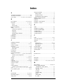
Table of Contents
Chapter 1. Introduction ........................................................................................................1
1.1 Summary of Design Conventions ...............................................................................................1
Chapter 2. Rabbit Hardware Design Overview ...................................................................3
2.1 Design Conventions ....................................................................................................................3
Rabbit Programming Connector ..........................................................................................4
Memory Chips .....................................................................................................................4
Oscillator Crystals................................................................................................................4
2.2 Operating Voltages ......................................................................................................................5
2.3 Power Consumption ....................................................................................................................5
2.4 Through-Hole Technology ..........................................................................................................6
2.5 Moisture Sensitivity ....................................................................................................................6
Chapter 3. Core Design and Components............................................................................7
3.1 Clocks..........................................................................................................................................7
3.2 Floating Inputs.............................................................................................................................8
3.3 Basic Memory Design .................................................................................................................8
Memory Access Time ..........................................................................................................9
Interfacing External I/O with Rabbit 3000 Designs ............................................................9
3.4 PC Board Layout and Memory Line Permutation ....................................................................10
3.5 PC Board Layout and Electromagnetic Interference.................................................................10
Rabbit 3000 Low EMI Features.........................................................................................10
Chapter 4. How Dynamic C Cold Boots the Target System..............................................11
4.1 How the Cold Boot Mode Works In Detail...............................................................................12
4.2 Program Loading Process Overview.........................................................................................13
Program Loading Process Details......................................................................................13
Chapter 5. Rabbit Memory Organization..........................................................................15
5.1 Physical Memory.......................................................................................................................15
Flash Memory ....................................................................................................................15
SRAM ................................................................................................................................15
Basic Memory Configuration ............................................................................................16
5.2 Memory Segments.....................................................................................................................16
Definition of Terms............................................................................................................17
The Base (or Root) Segment..............................................................................................17
Types of Code Best-Suited for the Base Segment ..............................................18
The Data Segment..............................................................................................................18
The Stack Segment ............................................................................................................18
The Extended Memory Segment .......................................................................................18
5.3 Separate I&D Space ..................................................................................................................19
Enable Separate I&D Space...............................................................................................21
I&D Space Mappings in Dynamic C .................................................................................21
Compiling to RAM .............................................................................................22
Compiling to Flash .............................................................................................23
Writing a Flash Driver .......................................................................................................24
Customizing Interrupts ......................................................................................................25
Method #1 ...........................................................................................................26
Method #2 ...........................................................................................................27
5.4 How The Compiler Compiles to Memory.................................................................................28
Placement of Code in Memory ..........................................................................................28
Designer’s Handbook
Paged Access in Extended Memory.................................................................................. 28
5.5 Memory Planning ..................................................................................................................... 29
Flash ............................................................................................................................... 29
Static RAM........................................................................................................................ 29
5.6 Making a RAM-Only Board..................................................................................................... 30
Hardware Changes ............................................................................................................ 30
Software Changes.............................................................................................................. 30
Chapter 6. The Rabbit BIOS..............................................................................................31
6.1
6.2
6.3
6.4
Startup Conditions Set by the BIOS ......................................................................................... 32
BIOS Flowchart ........................................................................................................................ 33
Internally-Defined Macros........................................................................................................ 34
Modifying the BIOS ................................................................................................................. 34
Advanced Options ............................................................................................................. 36
6.5 Origin Directives Used by the Compiler .................................................................................. 37
Origin Directive Syntax .................................................................................................... 37
Origin Directive Semantics .............................................................................................. 38
Defining a Memory Region ............................................................................... 38
Action Qualifiers ................................................................................................ 38
I&D Qualifiers ................................................................................................... 39
Follow Qualifiers ............................................................................................... 39
Origin Directive Examples................................................................................................ 40
Origin Directives in Program Code................................................................................... 40
Chapter 7. The System Identification and User Blocks.....................................................41
7.1 System ID Block Details .......................................................................................................... 42
Definition of SysIDBlock.................................................................................................. 42
Reading the System ID Block ........................................................................................... 43
Determining the Existence of the System ID Block .......................................... 44
Writing the System ID Block ............................................................................................ 45
7.2 User Block Details.................................................................................................................... 46
Boot Block Issues.............................................................................................................. 46
Reserved Flash Space........................................................................................................ 47
Reading the User Block..................................................................................................... 48
Writing the User Block..................................................................................................... 50
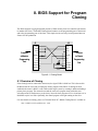
Chapter 8. BIOS Support for Program Cloning.................................................................53
8.1 Overview of Cloning ................................................................................................................ 53
8.2 Creating a Clone ....................................................................................................................... 54
Steps to Enable and Set Up Cloning ................................................................................. 54
Steps to Perform Cloning .................................................................................................. 54
LED Patterns ..................................................................................................................... 54
8.3 Cloning Questions .................................................................................................................... 55
MAC Address.................................................................................................................... 55
Different Flash Types ........................................................................................................ 55
Different Memory Sizes .................................................................................................... 55
Design Restrictions ........................................................................................................... 55
Rabbit 3000 Microprocessor
Chapter 9. Low-Power Design and Support ......................................................................57
9.1 Details of the Rabbit 3000 Low-Power Features ......................................................................58
Special Chip Select Features..............................................................................................58
Reducing Operating Voltage ..............................................................................................59
Preferred Crystal Configuration.........................................................................................59
9.2 To Further Decrease Power Consumption ................................................................................60
What To Do When There is Nothing To Do ......................................................................60
Sleepy Mode ......................................................................................................................60
External 32 kHz Oscillator ................................................................................................61
Conformal Coating of 32.768 kHz Oscillator Circuit........................................................61
Software Support for Sleepy Mode ...................................................................................61
Baud Rates in Sleepy Mode...............................................................................................62
Debugging in Sleepy Mode ...............................................................................................62
Chapter 10. Supported Flash Memories ............................................................................63
10.1 Supporting Other Flash Devices .............................................................................................63
10.2 Writing Your Own Flash Driver ..............................................................................................64
Required Information for Flash Memory...........................................................................64
Flash Driver Functions.......................................................................................................65
Chapter 11. Troubleshooting Tips for New Rabbit-Based Systems ..................................67
11.1 Initial Checks...........................................................................................................................67
11.2 Diagnostic Tests.......................................................................................................................67
Program to Transmit Diagnostic Tests...............................................................................67
Diagnostic Test #1: Toggle the Status Pin .........................................................................69
Using serialIO.exe ..............................................................................................69
Diagnostic Test #2..............................................................................................................70
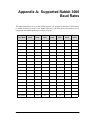
Appendix A.Supported Rabbit 3000 Baud Rates ..............................................................73
Notice to Users.................................................................................................................. 75
Index ................................................................................................................................. 77
Designer’s Handbook
Rabbit 3000 Microprocessor
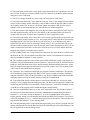
1. Introduction
This manual is intended for the engineer designing a system using the Rabbit 3000 microprocessor
and Z-World’s Dynamic C development environment. It explains how to develop a system that is
based on the Rabbit 3000 and can be programmed with Dynamic C.
With Rabbit 3000 microprocessors and Dynamic C, many traditional tools and concepts are obsolete. Complicated and fragile in-circuit emulators are unnecessary. EPROM burners are not
needed. Rabbit 3000 microprocessors and Dynamic C work together without elaborate hardware
aids, provided that the designer observes certain design conventions.
For all topics covered in this manual, further information is available in the Rabbit 3000 Microprocessor User’s Manual.
1.1 Summary of Design Conventions
• Include a programming connector.
• Connect a static RAM having at least 128 KB to the Rabbit 3000 using
/CS1, /OE1 and /WE1.
• Connect a flash memory that is on the approved list and has at least 128 KB
of storage to the Rabbit 3000 using /CS0, /OE0 and /WE0.
• Install a crystal oscillator with a frequency of 32.768 kHz to drive the battery-backable clock. (Battery-backing is optional, but the clock is used in
the cold boot sequence to generate a known baud rate of 2400 bps.)
• Install a crystal or oscillator for the main processor clock that is a multiple
of 614.4 kHz, or better, a multiple of 1.8432 MHz.
• Do not use pin PB1 in your design if cloning is to be used.
• Be sure unused inputs are not floating.
Designer’s Handbook
1
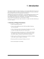
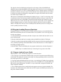
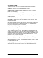
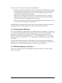
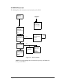
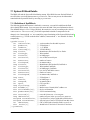
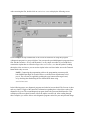
As shown in Figure 1, the Rabbit programming cable connects a PC serial port to the programming connector of the target system. Dynamic C or the Rabbit Field Utility (RFU) runs as an
application on the PC, and can cold boot the Rabbit 3000 based target system with no pre-existing
program installed in the target. A USB to RS232 converter may also be used instead of a PC serial
port. Rabbit 3000 based targets may also be programmed and debugged remotely over a local network or even the Internet using a RabbitLink card.
PC Hosts Dynamic C
Rabbit Programming
Cable
Level
Conversion
PC Serial
Port
Rabbit
Microprocessor
Target
System
Programming
Connector
Figure 1.1 The Rabbit 3000 Microprocessor and Dynamic C
Dynamic C programming uses serial port A for software development. However, it is possible for
the user’s application to also use serial port A, with the restriction that debugging is not available.
2
Rabbit 3000 Microprocessor
2. Rabbit Hardware Design
Overview
Because of the glueless nature of the external interfaces, especially the memory interface, it is easy
to design hardware in a Rabbit 3000-based system. More details on hardware design are given in
the Rabbit 3000 Microprocessor User’s Manual.
2.1 Design Conventions
• Include a standard Rabbit programming cable. The standard 10-pin programming connector
provides a connection to serial port A and allows the PC to reset and cold boot the target
system.
• Connect a static RAM having at least 128 KB to the processor using /CS1, /OE1 and /WE1.
It is useful if the PC board footprint can also accommodate a RAM large enough to hold all
the code anticipated. Although code residing in some flash memory can be debugged,
debugging and program download is faster to RAM.
• Connect a flash memory that is on the approved list and has at least 128 KB of storage to
the processor using /CS0, /OE0 and /WE0. Non-approved memories can be used, but it may
be necessary to modify the BIOS. Some systems designed to have their program reloaded
by an external agent on each powerup may not need any flash memory.
• Install a crystal oscillator with a frequency of 32.768 kHz to drive the battery-backable realtime clock (RTC), the watchdog timer (WDT) and the Periodic Interrupt.
• Install a crystal or oscillator for the main processor clock that is a multiple of 614.4 kHz, or
better, a multiple of 1.8432 MHz. These preferred clock frequencies make possible the generation of sensible baud rates. Common crystal frequencies to use are 7.3728 MHz,
11.0592 MHz, 14.7456 MHz, 18.432 MHz, 22.1184 MHz, 25.8048 MHz or double these
frequencies.
• Digital I/O line PB1 should not be used in the design if cloning is to be used. PB1 should be
pulled up with 50K or so pull up resistor if cloning is used. (See “BIOS Support for Program Cloning” on page 53 for more information on cloning.)
Designer’s Handbook
3
2.1.1 Rabbit Programming Connector
The user may be concerned that the requirement for a programming connector places added cost
overhead on the design. The overhead is very small—less than $0.25 for components and board
space that could be eliminated if the programming connector were not made a part of the system.
The programming connector can also be used for a variety of other purposes, including user applications. A device attached to the programming connector has complete control over the system
because it can perform a hardware reset and load new software. If this degree of control is not
desired for a particular situation, then certain pins can be left unconnected in the connecting cable,
limiting the functionality of the connector to serial communications. Z-World develops products
and software that assume the presence of the programming connector.
2.1.2 Memory Chips
Most systems have one static RAM chip and one or two flash memory chips, but more memory
chips can be used when appropriate. Static RAM chips are available in 32K x 8, 64K x 8, 128K x
8, 256K x 8 and 512K x 8 sizes. They are all available in 3 V versions. Suggested flash memory
chips between 128K x 8 and 512K x 8 are given in Chapter 10, Flash Memories.
Dynamic C and a PC are not necessary for the production programming of flash memory since the
flash memory can be copied from one controller to another by cloning. This is done by connecting
the system to be programmed to the same type of system that is already programmed. This connection is made with the Rabbit Cloning Board. The Cloning Board connects to the programming
ports of both systems. A push of a button starts the transfer of the program and an LED displays
the progress of the transfer.
Please visit http://www.zworld.com/store/index.html to purchase the Rabbit Cloning Board.
2.1.3 Oscillator Crystals
Generally, a system will have two oscillator crystals:
• A 32.768 kHz crystal oscillator to drive the battery-backable timer,
• A crystal that has a frequency that is a multiple of 614.4 kHz or a multiple of 1.8432 MHz.
Typical values are 1.8432, 3.6864, 7.3728, 11.0592, 14.7456, 18.432, 25.8048, and 29.4912
MHz.
These crystal frequencies (except 614.4 kHz and 1.8432 MHz) allow generation of standard baud
rates up to at least 115,200 bps. The clock frequency can be doubled by an on-chip clock doubler,
but the doubler should not be used to achieve frequencies higher than about 54 MHz on a 3.3 V
system. A quartz crystal should be used for the 32.768 kHz oscillator. For the main oscillator, a
ceramic resonator that is accurate to 0.5% will usually be adequate and less expensive than a
quartz crystal.
4
Rabbit 3000 Microprocessor
2.2 Operating Voltages
The operating voltage in Rabbit 3000 based systems will usually be 3.3 V ±10%, but voltages in
the range of 1.8 V to 2.7 V are also possible. The maximum computation per watt is obtained in
the range of 3.0 V to 3.6 V. The highest clock speed requires 3.3 V. The maximum clock speed
with a 3.3 V supply is 54 MHz (26.7264 x 2), but it will usually be convenient to use a 14.7456
MHz crystal, doubling the frequency to 29.4912 MHz. Good computational performance, but not
the absolute maximum, can be implemented for a 3.3 V system by using an 11.0592 crystal and
doubling the frequency to 22.1184 MHz. Such a system will operate with 70 ns memories. A
29.4912 MHz system will require memories with 55 ns access time. A table of timing specification is in the Rabbit 3000 Microprocessor User’s Manual.
2.3 Power Consumption
The following mechanisms are important for determining the current consumption of the Rabbit
3000 while it is operating.
1. A current proportional to voltage and clock frequency that results from the charging of
internal and external capacitances. At 3.3 V (see 2 below) approximately 57% of the current is
due to charging and 43% to crossover current.
2. Current is proportional to clock frequency and to VC = V(0.5 x V - 0.7). This is the crossover current that results from a brief short circuit when both the P and N transistors of a CMOS
buffer are turned on at the same time. This component drops as the voltage drops relative to the
other component, and becomes negligible at 1.4 V.
3. The current consumed by the built-in main oscillator when it is turned on. This current is
proportional to VC above, and is equal to 1 mA at 3.3 V.
4. The current drawn by the logic that is driven at the oscillator (crystal) frequency. This is
considered distinctly because it varies with the crystal frequency, but is not reduced when the
clock frequency is divided. This current becomes zero if the main oscillator is turned off. This
current is 2.5 mA at 3.3 V when the crystal frequency is 14.7 MHz. This current is divided
between capacitive and crossover components in the same manner as the currents in (1) and (2)
above.
All of the above components can be combined in the following formula:
I TOTAL = 0.32 × V × f + 0.23 × Vc × f + 0.30 × Vc + 0.029 × V × fc + 0.025 × Vc × fc
where,
Vc = V × ( 0.5 × V – 0.7 )
fc = frequency of crystal oscillator
f = clock frequency in MHz
Designer’s Handbook
5
2.4 Through-Hole Technology
Most design advice given for the Rabbit 3000 assumes the use of surface-mount technology. However, it is possible to use the older through hole technology and develop a Rabbit 3000 system.
One can use Z-World’s Rabbit 3000-based Core Module, a small circuit board with a complete
Rabbit 3000 core that includes memory and oscillators. Another possibility is to solder the Rabbit
3000 processors by hand to the circuit board. This is not difficult and is satisfactory for low production volumes if the right technique is used.
2.5 Moisture Sensitivity
Surface-mount processing of plastic packaged components such as Rabbit microprocessors typically involves subjecting the package body to high temperatures and various chemicals such as
solder fluxes and cleaning fluids during solder wave and reflow operations. The plastic molding
compounds used for IC packaging (encapsulation) is hygroscopic, that is, it readily absorbs moisture. The amount of moisture absorbed by the package is proportional to the storage environment
and the amount of time the package is exposed to the humidity in the environment. During the solder reflow process, the package is heated rapidly, and any moisture present in the package will
vaporize rapidly, generating excessive internal pressures to various interfaces in the package. The
vapors escaping from the package may cause cracks or delamination of the package. These cracks
can propagate through the package or along the lead frame, thus exposing the die to ionic contaminants and increasing the potential for circuit failures. The damage to the package may or may not
be visible to the naked eye. This condition is common to all plastic surface-mount components and
is not unique to Rabbit microprocessors.
Rabbit microprocessors are shipped to customers in moisture-barrier bags with enough desiccant
to maintain their contents below 20% relative humidity for up to 12 months from the date of seal.
A reversible Humidity Indicator Card is enclosed to monitor the internal humidity level. The
loaded bag is then sealed under a partial vacuum. The caution label (IPC/JEDEC J-STD-020,
LEVEL 3) included with each bag outlines storage, handling, and bake requirements.
The requirements outlined on the label only apply to components that will be exposed to SMT processing. This means that completed board-level products that will not be subjected to the solder
reflow processing do not have to be baked or sealed in special moisture barrier bags.
6
Rabbit 3000 Microprocessor
3. Core Design and Components
Core designs can be developed around the Rabbit 3000 microprocessor. A core design includes
memory, the microprocessor, oscillator crystals, the Rabbit 3000 standard programming port, and
in some cases, a power controller and power supply. Although modern designs usually use at least
four-layer printed circuit boards, two-sided boards are a viable option with the Rabbit 3000,
especially if the clock speed is not high and the design is intended to operate at 2.5 V or 3.3 V—
factors that reduce edge speed and electromagnetic radiation.
Schematics illustrating the use of the Rabbit 3000 microprocessor are available at:
www.rabbitsemiconductor.com
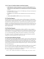
3.1 Clocks
The Rabbit 3000 has a built-in oscillator for the fast clock and an input pin for the 32.768 kHz
clock. The fast clock drives the Rabbit 3000 CPU and peripheral clocks, whereas the 32.768 kHz
clock is used for the battery backable clock (aka, the real-time clock), the watchdog timer, the
periodic interrupt timer and the asynchronous cold boot function.
XTALB2
2 kW
1 MW
XTALB1
33 pF
11.0592 MHz
(for example)
33 pF
Figure 3-1 Main Oscillator Circuit
The 32.768 kHz oscillator is slow to start oscillating after power-on. For this reason, a wait loop in
the BIOS waits until this oscillator is oscillating regularly before continuing the startup procedure.
The startup delay may be as much as 5 seconds, but will usually be about 200 ms. Crystals with
low series resistance ( R < 35 kΩ) will start faster.
For more information on the 32.768 kHz oscillator please see Technical Note 235, “External
32.768 kHz Oscillator Circuits.” This document is available on our website:
www.rabbitsemiconductor.com.
Designer’s Handbook
7
3.2 Floating Inputs
Floating inputs or inputs that are not solidly either high or low can draw current because both N
and P FETs can turn on at the same time. To avoid excessive power consumption, floating inputs
should not be included in a design (except that some inputs may float briefly during power-on
sequencing). Most unused inputs on the Rabbit 3000 can be made into outputs by proper software
initialization to remove the floating property. Pull-up resistors will be needed on a few inputs that
cannot be programmed as outputs. An alternative to a pull-up resistor is to tie an unused output to
the unused inputs. If pull-up (or pull-down) resistors are required, they should be made as large as
possible if the circuit in question has a substantial part of its duty cycle with current flowing
through the resistor.
3.3 Basic Memory Design
Normally /CS0 and /OE0 and /WE0 should be connected to a flash memory that holds the startup
code that executes at address zero. When the processor exits reset with (SMODE1, SMODE0) set
to (0,0), it will attempt to start executing instructions at the start of the memory connected to /CS0,
/OE0, and /WE0.
For Dynamic C to work out of the box, the basic RAM memory must be connected to /CS1, /OE1,
and /WE1.
/CS1 has a special property that makes it the preferred chip select for battery-backed RAM. The
BIOS defined macro, CS1_ALWAYS_ON, may be redefined in the BIOS to 1which will set a bit in
the MMIDR register that forces /CS1 to stay enabled (low). This capability can be used to counter
a problem encountered when the chip select line is passed through a device that is used to place
the chip in standby by raising /CS1 when the power is switched over to battery backup. The battery switchover device typically has a propagation delay that may be 20 ns or more. This is enough
to require the insertion of wait states for RAM access in some cases. By forcing /CS1 low, the
propagation delay is not a factor because the RAM will always be selected and will be controlled
by /OE1 and /WE1. If this is done, the RAM will consume more power while not battery-backed
than it would if it were run with dynamic chip select and a wait state. If this special feature is used
to speed up access time for battery backed RAM then no other memory chips should be connected
to OE1 and WE1.
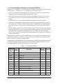
Table 3.1 Typical Interface between the Rabbit 3000 and Memory
Primary Flash
/CS0, /OE0 and /WE0
8
SRAM
/CS1, /OE1 and /WE1
Secondary Flash
/CS2, /OE0 and /WE0
Rabbit 3000 Microprocessor
3.3.1 Memory Access Time
Memory access time depends on the clock speed and the capacitive loading of the address and data
lines. Wait states can be specified by programming to accommodate slow memories for a given
clock speed. Wait states should be avoided with memory that holds programs because there is a
significant slowing of the execution speed. Wait states are far more important in the instruction
memory than in the data memory since the great majority of accesses are instruction fetches.
Going from 0 to 1 wait states is about the same as reducing the clock speed by 30%. Going from 0
to 2 wait states is worth approximately a 45% reduction in clock speed. A table of memory access
times required for various clock speeds is given in the Rabbit 3000 Microprocessor User’s
Manual.
3.3.2 Interfacing External I/O with Rabbit 3000 Designs
The Rabbit 3000 provides on-chip facilities for glueless interfacing to many types of external I/O
peripherals. The processor provides a common I/O read and I/O write strobe in addition to eight
user configurable I/O strobes that can be used as read, write, read/write, or chip select signals. The
Rabbit 3000 also provides the option of enabling a completely separate bus for I/O accesses. The
Auxiliary I/O Bus, which uses many of the same pins used by Parallel Port A and the Slave Port,
provides 8 data lines and 6 address lines that are active only during I/O operations. By connecting
I/O devices to the auxiliary bus, the fast memory bus is relieved of capacitive loading that would
otherwise slow down memory accesses. For core modules based on the Rabbit 3000, fewer pins
are required to exit the core module since the slave port and the I/O bus can share the same pins
and the memory bus no longer needs to exit the module to provide I/O capability.
As far as external I/O timing is concerned, the Rabbit 3000 provides:
• half a clock cycle of address and chip select hold time for I/O write operations, and
• zero clock cycles of address and chip select hold times for I/O read operations.
This is true if an I/O device is interfaced to the common memory and I/O bus. However, if an I/O
peripheral is interfaced to the Auxiliary I/O bus, address hold time is no longer an issue as the
address does not change until the next external I/O operation. For more information on I/O timing
please refer to the Rabbit 3000® Microprocessor User's Manual.
Some I/O peripherals such as LCD controllers and Compact Flash devices require address and
chip select hold times for both read and write operations. If the peripheral is interfaced to the Auxiliary I/O bus, address hold time is not an issue. If chip select hold time is required, an unused auxiliary I/O address line can be used to generate the chip select. In situations where I/O peripherals
are interfaced to the common memory and I/O bus, address and chip select hold times can be
extended under software control or with minor hardware changes. Please refer to Technical Note
227, "Interfacing External I/O with Rabbit 2000/3000 Designs" for additional information. This
document is available online:
http://www.rabbitsemiconductor.com/docs/app_tech_notes.shtml
Designer’s Handbook
9
3.4 PC Board Layout and Memory Line Permutation
In order to use the PC board real estate efficiently, it is recommended that the address and data
lines to memory be permuted to minimize the use of PC board resources. By permuting the lines,
the need to have lines cross over each other on the PC board is reduced, saving feed-through’s and
space.
For static RAM, address and data lines can be permuted freely, meaning that the address lines
from the processor can be connected in any order to the address lines of the RAM, and the same
applies for the data lines. For example, if the RAM has 15 address lines and 8 data lines, it makes
no difference if A15 from the processor connects to A8 on the RAM and vice versa. Similarly D8
on the processor could connect to D3 on the RAM. The only restriction is that all 8 processor data
lines must connect to the 8 RAM data lines. If several different types of RAM can be accommodated in the same PC board footprint, then the upper address lines that are unused if a smaller
RAM is installed must be kept in order. For example, if the same footprint can accept either a
128K x 8 RAM with 17 address lines or a 512K x 8 RAM with 19 address lines, then address lines
A18 and A19 can be interchanged with each other, but not exchanged with A0–A17.
Permuting lines does make a difference with flash memory and must be avoided in practical systems.
3.5 PC Board Layout and Electromagnetic Interference
Most design failures are related to the layout of the PC board. A good layout results when the
effects of electromagnetic interference (EMI) are considered. For detailed information regarding
this subject please see Technical Note 221, “PC Board Layout Suggestion for the Rabbit 3000
Microprocessor.” This document is available at:
http://www.rabbitsemiconductor.com/docs/app_tech_notes.shtml
3.5.1 Rabbit 3000 Low EMI Features
The Rabbit 3000 has powerful built-in features to minimize EMI. They are noted here. For details
please see The Rabbit 3000 Microprocessor User’s Manual.
• Separate power pins exist for core and I/O rings.
• The I/O bus can be separate from the memory bus.
• The external processor bus cycles are not all the same length.
• The external processor bus does not require running the clock around the PCB.
• The clock spectrum spreader option modulates the clock frequency.
• Some gated internal clocks are enabled only when needed.
• An internal clock doubler allows the external crystal oscillator to operate at 1/2 frequency.
10
Rabbit 3000 Microprocessor
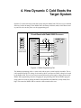
4. How Dynamic C Cold Boots the
Target System
Dynamic C assumes that target controller boards using the Rabbit 3000 CPU have no pre-installed
firmware. It takes advantage of the Rabbit 3000’s bootstrap (cold boot) mode, which allows memory and I/O writes to take place over the programming port.
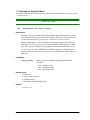
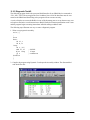
Circuit Board with Rabbit 3000 Processor
6
7
9
RXA
8
GND
10
CLKA
Vcc
Programming
Header Pinout
/RESET
TXA
n.c.
STATUS
SMODE0
51
2
GND
3
94
4
+3.3 V
5
37
6
54
7
8
38
9
36
10
35
~50 kW
SMODE1
1
~5 kW
4
5
RABBIT 3000
RXA
VSS
CLKA
VDD
/RESET
TXA
STATUS
SMODE0
SMODE1
~50 kW
3
Vcc
Programming
Header
~50 kW
2
~50 kW
1
Figure 4-1 Rabbit Programming Port
The Rabbit programming cable is a smart cable with an active circuit board in its middle. The circuit board converts RS-232 voltage levels used by the PC serial port to CMOS voltage levels used
by the Rabbit 3000. The level converter is powered from the power supply voltage present on the
Rabbit 3000 programming connector. Plugging the programming cable into the Rabbit programming connector results in pulling the Rabbit 3000 SMODE0 and SMODE1 (startup mode) lines
high. This causes the Rabbit 3000 to enter the cold boot mode after reset.
Designer’s Handbook
11
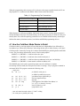
When the programming cable connects a PC serial port to the target controller board, the PC running Dynamic C is connected to the Rabbit 3000 as shown in the table below.
Table 4-1 Programming Port Connections
PC Serial Port Signal
Rabbit 3000 Signal
DTR (output)
/RESET (input, reset system)
DSR (input)
STATUS (general purpose output)
TX (serial output)
RXA (serial input, port A)
RX (serial input)
TXA (serial output, port A)
When Dynamic C cold boots the Rabbit 3000-based target system it assumes that no program is
already installed on the target. The flash memory on the target system may be blank or it may contain any data. The cold boot capability permits the use of soldered-in flash memory on the target.
Soldered-in memory eliminates sockets, boot blocks and PROM programming devices.
4.1 How the Cold Boot Mode Works In Detail
Cold boot works by receiving triplets of bytes that consist of a high address byte followed by a
low address byte, followed by a data byte, and writing the data byte to either memory or I/O space.
Cold boot mode is entered by having one or both of the SMODE pins pulled high when the Rabbit
is reset. The pin settings determine the source of the incoming triplets:
SMODE1 = 0, SMODE0 = 1 cold boot from slave port.
SMODE1 = 1, SMODE0 = 0 cold boot from clocked serial port A.
SMODE1 = 1, SMODE0 = 1 cold boot from asynchronous serial port A at 2400 bps.
SMODE1 = 0, SMODE0 = 0 start normal execution at address zero.
The SMODE pins can be used as general input pins once the cold boot is complete.
On entering cold boot mode, the microprocessor starts executing a 12-byte program contained in
an internal ROM. The program contains the following code.
; origin zero
00 ld l,n
02
04
06
08
ioi
ioi
ioi
ioi
ld
ld
ld
or
d,(hl)
e,(hl)
a,(hl)
nop
09
10
ld (de),A
jr 0
; n=0c0h for serial port A
; n=020h for parallel (slave port)
; get address most significant byte
; get least significant byte
; get data
; if the high bit of the MSB of the address is 1
; (i.e., d[7] ==1) then ioi, else nop
; store in memory or I/O
; jump back to zero
; note wait states inserted at bytes 3, 5 and 7 waiting
; for serial port or parallel port ready
12
Rabbit 3000 Microprocessor
The function of the boot ROM program depends on the settings of the pins SMODE0 and
SMODE1 and on whether the high bit of the high address byte (first byte of a received triplet) that
is loaded to register D is set. If bit 7 of the high address byte is set, then the data byte (last byte of
the triplet) is written to I/O space when received. If the bit is clear, then the data byte gets written
to memory. Boot mode is terminated by storing 80h to I/O register 24h, which causes an instruction fetch to begin at address zero.
Wait states are automatically inserted during the fetching of bytes 3, 5 and 7 to wait for the serial
or parallel port ready. The wait states continue indefinitely until the serial port is ready. This will
cause the processor to be in the middle of an instruction fetch until the next character is ready.
While the processor is in this state the chip select, but not the output enable, will be enabled if the
memory mapping registers are such as to normally enable the chip select for the boot ROM
address. The chip select will stay low for extended periods while the processor is waiting for the
serial or parallel port data to be ready.
4.2 Program Loading Process Overview
On start up, Dynamic C first uses the PC’s DTR line on the serial port to assert the Rabbit 3000
RESET line and put the processor in cold boot mode. Next, Dynamic C uses a four stage process
to load a user program:
1. Load an initial loader (cold loader) to RAM via triplets sent at 2400 baud from the PC to a target in cold boot mode.
2. Run the initial loader and load a secondary loader (pilot BIOS) to RAM at 57600 baud.
3. Run the secondary loader and load the BIOS and user program to flash after compiling them to
a file, optionally negotiating with the Pilot BIOS to increase the baud rate to 115200 or higher so
the loading can happen quickly.
4. Run the BIOS. Then run and debug the user program at the baud rate selected in Dynamic C.
NOTE: Step 4 is combined with step 3 when using 4 K (or greater) sector flash.
4.2.1 Program Loading Process Details
When Dynamic C starts, the following sequence of events takes place:
1. The serial port is opened with the DTR line high, closed, then reopened with the DTR line low
at 2400 baud. This pulses the reset line on the target low (the programming cable inverts the DTR
line) and prepares the PC to send triplets.
2. A group of triplets defined in the file COLDLOAD.BIN consisting of 2 address bytes and a data
byte are sent to the target. The first few bytes sent are sent to I/O addresses to set up the MMU and
MIU and do system initialization. The MMU is set up so that RAM is mapped to 0x00000, and
flash is mapped to 0x80000.
3. The remaining triplets place a small initial loader program at memory location 0x00000. The
last triplet sent is 0x80, 0x24, 0x80, which tells the CPU to ignore the SMODE pins and start running code at address 0x00000.
Designer’s Handbook
13
4. The initial loader measures the crystal speed to determine what divisor is needed to set a baud
rate of 19200. The divisor is stored at address 0x3F02 for later use by the BIOS, and the programming port is set to 57600 baud.
5. The PC now bumps the baud rate on the serial port being used to 57600 baud.
6. The initial loader then reads 7 bytes from the serial port. First a 2-byte length field: the number
of bytes in the secondary loader, followed by a 4-byte address field: the physical address to place
the secondary loader. The 7th byte is a checksum (simple summation) of the previous 6 bytes.
Whether or not the checksum matched, it is echoed back as an acknowledgement.
7. The data segment is then mapped to the given physical location, using the DATASEG register.
The data segment boundary will also be set to 0x6000, so the secondary loader will always be
located at the same place in logical space, regardless of where it physically resides.
8. The initial loader finally enters a loop where it receives the specified number of bytes that compose the secondary loader program (pilot.bin sent by the PC) and writes those bytes starting
at 0x6000 (logical). The first byte sent this way MUST be 0xCC, as an indicator to the initial
loader. This byte will be stored as 0x00 (nop), instead of 0xCC. A 2-byte checksum will be sent
after the secondary loader has been received, using the 8-bit Fletcher Algorithm (see RFC1145 for
details), such that the load can be verified. After all of the bytes are received, and the checksum
has been sent, program execution jumps to 0x6000.
9. The secondary loader does a wrap-around test to determine how much RAM is available, reads
the flash ID, the CPU ID, and initializes the flash-write routines. This information is made available for transmittal to Dynamic C when requested.
10. The secondary loader now enters a finite state machine (FSM) that is used to implement the
Dynamic C/Target Communications protocol. Dynamic C requests the CPU ID, flash information,
RAM size, and 19200 baud rate divisor to define internally defined constants and macros. At this
stage, the compiler can request the baud rate be increased to a higher value. The secondary loader
is now ready to load a BIOS and user program.
11. Dynamic C now compiles the BIOS and user programs. Both are compiled to a file, then the
file is loaded to the target using the Pilot BIOS’ FSM. After the loading is complete, Dynamic C,
using the Pilot BIOS’ FSM, tells the Pilot BIOS to map flash to 0x00000, map RAM to 0x80000,
and start program execution at 0x0000, thereby running the compiled BIOS.
12. If the Pilot BIOS detects a RAM compile or small-sector flash that uses sector-write mode,
Dynamic C uses a slightly different loading procedure. The BIOS will be compiled as normal, and
loaded using the Pilot BIOS. After the BIOS is loaded, Dynamic C will tell the Pilot BIOS to start
it, and the rest of the program will be loaded through the compiled BIOS.
13. Once the compiled BIOS starts up, it runs some initialization code. This includes setting up
the serial port for the debug baud rate (set in the Communications Options dialog box prior to
Dynamic C v. 8. For later versions of Dynamic C, go to the Communications tab in Options |
Project Options), setting up serial interrupts and starting the BIOS FSM. Dynamic C sets a breakpoint at the beginning of main() and runs the program up to the breakpoint. The board has been
programmed, and Dynamic C is now in debug mode.
14. If the programming cable is removed and the target board is reset, the user’s program will start
running automatically because the BIOS will check the SMODE pins to determine whether to run
the user application or enter the debug kernel.
14
Rabbit 3000 Microprocessor
5. Rabbit Memory Organization
The Rabbit 3000 architecture is derived from the original Z80 microprocessor. The original Z80
instruction set used 16-bit addresses to address a 64 KB memory space. All code and data had to
fit in this 64 KB space. To expand the available memory space, the Rabbit 3000 adopts a scheme
similar to that used by the Z180. The 64 KB space is divided into segments and the Rabbit’s Memory Mapping Unit (MMU) maps each segment to a block in a larger memory. The larger memory
is 1 megabyte. The segments are effectively windows to the larger memory. The view from the
window can be adjusted so that the window looks at different blocks in the larger memory.
Figure 5-1 on page 16 shows the memory mapping schematically.
Please see Technical Note 202, “ Rabbit Memory Management in a Nutshell,” for more details on
how memory mapping works. This document is available at:
http://www.rabbitsemiconductor.com/docs/app_tech_notes.shtml
5.1 Physical Memory
The Rabbit 3000 has a 1 MB physical memory space. In special circumstances more than 1 MB of
memory can be installed and accessed using auxiliary memory mapping schemes. Typical
Rabbit 3000 systems have two types of physical memory: flash memory and static RAM memory.
5.1.1 Flash Memory
Flash memory in a Rabbit 3000-based system may be small-sector or large-sector type. Small-sector memory typically has sectors of 128 to 4096 bytes. Individual sectors may be separately erased
and written. In large-sector memory the sectors are often 16 KB to 64 KB or more. Large-sector
memory is less expensive and has faster access time. The best solution will usually be to lay out a
design to accept several different types of flash memory, including the flexible small-sector memories and the fast large-sector memories.
Flash memory follows a write-once-in-a-while and read-frequently model. Depending on the particular type of flash used, the flash memory may wear out after it has been written approximately
10,000 to 100,000 times.
5.1.2 SRAM
Static RAM memory may or may not be battery-backed. If it is battery-backed it retains its data
when power is off. Static RAM chips typically used for Rabbit systems are 128 KB, 256 KB, or
512 KB.
When the memory is battery-backed, power is supplied at 2 V to 3 V from a backup battery. While
preserving memory contents with battery power, the shutdown circuitry must keep the chip select
line high.
Designer’s Handbook
15
5.1.3 Basic Memory Configuration
A basic Rabbit system typically has two static memory chips: one flash memory chip and one
RAM chip. Additional static memory chips may be added. If an application requires storing a lot
of data in flash memory, it is recommended that another flash memory chip be added, creating a
system with 3 memory chips—2 flash memory chips and one RAM chip.
Trying to use a single flash memory chip to store both the user’s program and live data that must
be frequently changed can create software problems. When data are written to a small-sector flash
memory, the memory becomes inoperative during the 5 to 20 ms that it takes to write a sector. If
the same memory chip is used to hold data and the program, then the execution of code must cease
during this write time. The 5-20 ms is timed out by a small routine executing from root RAM
while system interrupts are disabled, effectively freezing the system for 5-20 ms. The 5-20 ms
lockup period can seriously affect real-time operation.
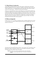
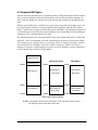
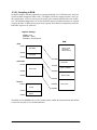
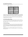
5.2 Memory Segments
From the point of view of a Dynamic C programmer, there are a number of different uses of memory. Each memory use occupies a different segment in the logical 16-bit address space. The four
segments are shown here:
1 MB
Quandrant 3
64 KB
Extended
Memory
Segment
56 KB
Stack
Segment
RAM
Quadrant 2
52 KB
Data
Segment
Quadrant 1
Base
Segment
Flash
(aka Root Segment)
Quadrant 0
0 KB
Logical Address Space
0 KB
Physical Address Space
Figure 5-1 Typical Memory Map of 16-bit Addressing Space
This figure shows that the Rabbit 3000 does not have a “flat” memory space. The advantage of the
Rabbit 3000’s memory organization is that the use of 16-bit addresses and pointers is retained,
ensuring that the code is compact and executes quickly.
NOTE: The relative size of the base and data segments can be adjusted by
increasing or decreasing the BIOS macro DATAORG in increments of
0x1000.
16
Rabbit 3000 Microprocessor
5.2.1 Definition of Terms
The following definitions clarify some of the terms that will be encountered in this chapter.
Extended Code: Instructions located in the extended memory segment.
Extended Constants: C constants located in the extended memory segment. They are mixed
together with the extended code.
Extended Memory: Logical addresses above 0xDFFF.
Extended RAM: RAM not used for root variables or stack. Extended memory in RAM may be
used for large buffers to save root RAM space. The function xalloc() allocates space in
extended RAM memory.
Root Code: Instructions located in the base segment.
Root Constants: C constants, such as quoted strings, initialized variables or data tables, that are
located in the base segment.
Root Memory: Logical addresses below 0xE000. Please note that root memory is not the same as
the root segment. The root segment is contained in root memory, as are the data and stack segments. The root segment is also known as the base segment.
Root Variables: C variables, including structures and arrays that are not initialized to a fixed
value, are located in the data segment.
5.2.2 The Base (or Root) Segment
The base segment has a typical size of 24 KB. The larger the base segment, the smaller the data
segment and vice-versa. Base segment address zero is always mapped to 20-bit address zero. Usually the base segment is mapped to flash memory since root code and root constants do not change
except when the system is reprogrammed. It may be mapped to RAM for debugging, or to take
advantage of the faster access time offered by RAM.
The base segment holds a mixture of code and constants. C functions or assembly language programs that are compiled to the base segment are interspersed with data constants. Data constants
are inserted between blocks of code. Data constants defined inside a C function are put before the
end of the code belonging to the function. Data constants defined outside of C functions are stored
as encountered in the source code.
Except in small programs, the bulk of the code is executed using the extended memory (xmem)
segment. Code operates at the same speed whether addressed through the base segment or the
xmem segment. It just takes a few cycles longer to call xmem functions and return from them.
Designer’s Handbook
17
5.2.2.1 Types of Code Best-Suited for the Base Segment
• Short subroutines of about 20 instructions or less that are called frequently will use
significantly less execution time if placed in root memory because of the faster calling linkage for 16-bit versus 20-bit addresses. For a call and return, 20 clocks are used compared to
32 clocks.
• Interrupt routines. Interrupt vectors use 16-bit addressing so the entry to an interrupt routine must be in the base segment.
• The BIOS core. The initialization code of the BIOS must be at the start of the base segment.
• A function that modifies the XPC must always be run in root memory.
5.2.3 The Data Segment
The data segment has a typical size of 28 KB, starting at 24 KB and ending at 52 KB (0xD000).
The data segment is mapped to RAM and contains C variables. Data allocation starts at or near the
top and proceeds in a downward direction. It is also possible to place executable code in the data
segment if it is copied from flash to the data segment. This can be desirable for code that is self
modifying, code to implement debugging aids or code that controls write to the flash memory and
cannot execute from flash. In some cases RAM may require fewer wait states so code executes
faster if copied to RAM.
5.2.4 The Stack Segment
Usually the stack segment is from logical address 0xD000 to 0xDFFF. It is always mapped to
RAM and holds the system stack. Multiple stacks may be implemented by defining several stacks
in the 4 KB space or by remapping the 4 KB space to different locations in physical RAM memory, or by using both approaches. Multiple stack allocation is handled by µC/OS-II internally.
For example, if 16 stacks of 1 KB length are needed then 4 stacks can be placed in each 4 KB
mapping and 4 different mappings for the window can be used.
5.2.5 The Extended Memory Segment
This 8 KB segment from logical address 0xE000 to 0xFFFF is used to execute extended code and
it is also used by routines that manipulate data located in extended memory. While executing code
the mapping is shifted by 4 KB each time the code passes the 60 KB point. Up to a MB of code
can be efficiently executed by moving the mapping of the 8 KB window using special instructions
(long call, long jump and long return) that are designed for this purpose. This uses up only 8 KB of
the 16-bit addressing space.
The xmem segment can map to any 4 KB page of the 1MB physical address space. For example if
XPC is set to 0xF2, then the 16-bit address 0xE000 maps to the physical address 0x00000.
Please see Technical Note 202, “Rabbit Memory Management in a Nutshell,” for more details on
how memory mapping works. This document is available at:
http://www.rabbitsemiconductor.com/docs/app_tech_notes.shtml
18
Rabbit 3000 Microprocessor
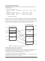
5.3 Separate I&D Space
Separate instruction and data space is a hardware memory management scheme that uses address
line inversion to double the amount of logical address space in the base and data segments. In
other words, this doubles the amount of root code and root data available for an application program.
Without separate I&D space, recall that in a typical memory map of the 16-bit address space, the
base segment holds a mixture of code and constants and is mapped to flash; the data segment
holds C variables and is mapped to RAM. With separate I&D space, code and data no longer have
to divide this space because they share logical addresses by inverting address lines depending on
whether the CPU is fetching instructions or data.
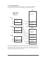
The following diagram shows the logical address space when separate I&D space is enabled and
SEGSIZE = 0xD3. The boundary at 0x3000 is determined by the macro DATAORG in the BIOS.
The boundary may be changed, however, care must be taken. To change the boundary, enter the
macro name and a new boundary value in the “Defines” dialog box, which is accessed via
Dynamic C’s Options | Compiler dialog box prior to version 8. With later versions of Dynamic C,
go to the Defines tab in Options | Project Options.
XMEM Segment
0xD000
Stack Segment
Instruction Space
0xD000
0xD000
Data Segment
Data Segment
0x3000
Data Segment
(Root Code)
Base Segment
(Root Data)
0x3000
0x3000
0x0000
Data Space
Base Segment
(Root Code)
0x0000
Base Segment
(Constants)
0x0000
16-bit Logical Address Space
NOTE: This diagram illustrates how I&D space works; the actual values used in
the BIOS may differ from those shown here.
Designer’s Handbook
19
I&D logical addresses map to physical addresses by inverting address lines A16, A19 or both. The
MMU Instruction/Data Register (MMIDR) determines which lines are inverted. Please see the
Rabbit 3000 Microprocessor User’s Manual for more information about the MMIDR.
The following diagram shows the physical address space when separate I&D space is enabled,
SEGSIZE = 0xD3 and code is compiled to flash.
0xFFFFF
512K RAM
0xC0000
0x8D000
44K
Root Data
0x83000
Invert
A19
0x80000
0x7FFFF
512K Flash
0x13000
8K
Root Constants
0x10000
Invert
A16
0x0D000
52K
Root Code
0x00000
The inversion of A16 causes the root constants in the data space to be addressed in the next higher
64 KB block of the flash. The inversion of A19 causes the root data in the data space to be
addressed in RAM (0x80000), starting at 0x83000 as directed by the lower nibble of SEGSIZE.
20
Rabbit 3000 Microprocessor
There are some new restrictions when using separate I&D space.
• Interrupt vectors that are modifiable at runtime have 80 clock cycles added to the execution
time of the interrupt. The default case for system defined interrupt vectors is nonmodifiable.
Nonmodifiable means that the interrupt vector is set at compile time and may not be
changed unless the application is recompiled.
• You can not reference code as data or data as code in logical memory below the stack.
When using separate I&D space, the processor makes a distinction between fetching an
instruction from memory and fetching data from memory.
• There are some changes in the flash driver that are handled internally. The changes are only
of concern if you are writing your own flash driver.
Embedded applications that do not need more code or data space need not make any changes for
separate I&D space. By default, Dynamic C compiles without I&D space enabled.
5.3.1 Enable Separate I&D Space
To use separate I&D space, open the Options | Compiler dialog box (for Dynamic C versions prior
to version 8) and check the enable separate I&D space option. For later versions of Dynamic C the
same option is accessible on the Compiler tab of the Options | Project Options dialog. The
Dynamic C command line compiler equivalent is -id+ (enable I&D space) and -id- (disable
I&D space). Please see the Dynamic C User’s Manual for more information about the command
line compiler.
The BIOS and the compiler take care of all the details so the user does not need to understand
them. However, if you want to change the way an interrupt vector is handled or you need to write a
flash driver, the rest of this chapter provides you with the necessary information.
5.3.2 I&D Space Mappings in Dynamic C
The next two subsections show the default MMU settings that Dynamic C uses when separate
I&D space is enabled.
Designer’s Handbook
21
5.3.2.1 Compiling to RAM
For RAM compiles, all banks (quadrants) are mapped to RAM. For 512 KB memories, the lower
256 KB would be mapped to banks 0 and 2. The higher 256 KB are mapped to banks 1 and 3. In
this configuration, A16 is inverted to provide access to the constants and data in the next 64 KB
area. The standard configuration is to set the SEGSIZE register to 0xDD so that the base segment
occupies the entire 52 KB region up to the stack segment. Note that this configuration causes the
DATASEG register to be irrelevant.
Register Settings
MMIDR = 0x21
SEGSIZE = 0xDD
DATASEG = 0x0 (irrelevant)
RAM
Data
0xCFFF
Xmem Code
continued,
xalloc, Stacks
Root Data
0x3000
Constants
0x0000
0x1D000
Instruction
Root Data
0xCFFF
0x3000
0x13000
Root Code
Root Constants
0x10000
Xmem Code
0x0000
0x0D000
Shared
0xFFFF
0x03000
Xmem
0xE000
0xD000
Root Code
0x00000
Stack
The BIOS sets the MMIDR to 0x21. Bit 5 of this register enables the instruction/data split and bit
0 causes the inversion of A16 for data addresses.
22
Rabbit 3000 Microprocessor
5.3.2.2 Compiling to Flash
For flash compiles, flash memory is mapped to banks 0 and 1 (address range 0x00000 to
0x7FFFF). RAM is mapped to banks 2 and 3 (address range 0x80000 to 0xFFFFF).
RAM
Register Settings
MMIDR = 0x29
SEGSIZE = 0xD3
DATASEG = 0x0
Stacks, xalloc,
etc.
Data
0xCFFF
Root Data
0x8D000
0x3000
Constants
Root Data
0x83000
0x0000
Instruction
0x80000
0xCFFF
Flash
Root Code
0x3000
Stack Space/
Watch Code
Root Code
Xmem Code
continued
0x0000
0x13000
Shared
0x10000
0xFFFF
Xmem
0xE000
0xD000
Root Constants
Xmem Code
0x0D000
Stack
Root Code
0x03000
0x00000
Root Code
The BIOS sets the MMIDR to 0x29 to enable the I&D space for flash compilation. Bit 5 of this
register enables the I&D split, bit 0 enables inversion of A16 for the data space base segment (i.e.,
the logical address space for constants) and bit 3 enables inversion of A19 for the data space data
segment (i.e., the logical address space for root data).
Designer’s Handbook
23
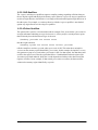
5.3.3 Writing a Flash Driver
If you are writing your own flash driver, please read Section 10.2, “Writing Your Own Flash
Driver,” starting on page 64. When using separate I&D space there are several additional things to
consider:
• The flash driver must run in RAM so that any flash location can be written.
• The flash driver cannot run in the xmem window for two reasons. First, the driver uses the
xmem window. Second, it would require the use of “load physical” instructions (ldp)
which always write 2 bytes and a flash unlock sequence requires 1-byte writes.
• Separate I&D space must be disabled while the flash driver is running due to the reasons
stated above.
• While the flash driver is running you lose access to most of the application code and to all
of its constants.
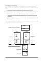
The following figure illustrates what happens to the access of an application’s code and data when
separate I&D space is disabled to run the flash driver.
Xmem
Separate I&D Space Enabled
Stack
Data Segment
Base Segment
I Space
D Space
Code
Data
A
B
Constants
Code
D
C
Data Segment
Base Segment
Xmem
Separate I&D Space Disabled
Data Segment
Base Segment
24
Stack
Data
B
Code
C
Rabbit 3000 Microprocessor
5.3.4 Customizing Interrupts
There are two methods to set the handling of an interrupt vector. The one you select depends on
the needs of your application. Most of the ISRs set up by the BIOS are fast and nonmodifiable by
default. Modifiable interrupts are slower because 80 clocks are added to their execution time.
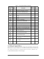
Here is a list of the defined interrupt vector names and the corresponding ISRs:
Table 5-1 Interrupt Vector and ISR Names
Interrupt Vector Name
ISR Name
Default Condition
periodic_intvec
periodic_isr
Fast and nonmodifiable
rst10_intvec
User defined name
User defined
rst18_intvec
These interrupt vectors and their ISRs should never be altered
by the user because they are reserved for the debug kernel.
rst20_intvec
rst28_intvec
rst38_intvec
User defined name
User defined
slave_intvec
slave_isr
Fast and nonmodifiable
timera_intvec
User defined name
User defined
timerb_intvec
User defined name
User defined
DevMateSerialISR
Fast and nonmodifiable
spa_isr
User defined
serb_intvec
spb_isr
User defined
serc_intvec
spc_isr
serd_intvec
spd_isr
sere_intvec
spe_isr
serf_intvec
spf_isr
inputcap_intvec
User defined name
quad_intvec
qd_isr
ext0_intvec
User defined name
ext1_intvec
User defined name
sera_intveca
a. Please note that this ISR shares the same interrupt vector as DevMateSerialISR.
Using spa_isr precludes Dynamic C from communicating with the target.
Designer’s Handbook
25
5.3.4.1 Method #1
To make an ISR fast and nonmodifiable, use the keyword interrupt_vector. The syntax is:
interrupt_vector <INT_VECTOR_NAME> <ISR_NAME>
INT_VECTOR_NAME is an interrupt vector name, either user-defined or from Table 5-1.
ISR_NAME is the name of the interrupt service routine, either user-defined or from Table 5-1. The
interrupt vectors for user-defined ISRs are fast and nonmodifiable when interrupt_vector
is used during setup.
In an application, use as follows:
// Set up an Interrupt Service Routine for Timer B
#asm
timerb_isr::
; ISR code
...
ret
#endasm
main() {
// Variables
...
// Set up ISR
interrupt_vector timerb_intvec timerb_isr; // Compile time set up
// Code
...
}
Notice that the interrupt vector is set up at compile time. This will override any run-time set up
done by the function SetVectIntern(). Therefore, this function and the
interrupt_vector keyword are mutually exclusive. In other words, if you use both, the
interrupt vector handling will be determined by interrupt_vector and not by
SetVectIntern(). Additionally, if interrupt_vector is used multiple times for the
same interrupt vector, the last one encountered by the compiler will override all previous ones.
For more information on SetVectIntern(), please see the Dynamic C Function Reference
Manual or use the Function Lookup feature from Dynamic C’s Help menu.
The keyword interrupt_vector is syntactic sugar for using the origin directives and assembly code. The line:
interrupt_vector timerb_intvec timerb_isr;
is equivalent to the following:
#rcodorg timerb_intvec apply
#asm
jp timerb_isr
#endasm
#rcodorg rootcode resume
26
Rabbit 3000 Microprocessor
5.3.4.2 Method #2
If you want the ISR to be modifiable, you have to set it up as follows:
#rcodorg <INT_VEC_NAME> apply
#asm
INTVEC_RELAY_SETUP(intvec_relay + <INTERRUPT_OFFSET>)
#endasm
#rcodeorg rootcode resume
<INTERRUPT_OFFSET> is one of the following:
EXT0_OFS
EXT1_OFS
INPUTCAP_OFS
PERIODIC_OFS
QUAD_OFS
RST10_OFS
RST18_OFS
RST20_OFS
RST28_OFS
RST38_OFS
SERA_OFS
SERB_OFS
SERC_OFS
SERD_OFS
SERE_OFS
SERF_OFS
SLAVE_OFS
TIMERA_OFS
TIMERB_OFS
These are defined in sysio.lib.
Designer’s Handbook
27
5.4 How The Compiler Compiles to Memory
The compiler generates code for root code, root constants, extended code and extended constants.
It allocates space for data variables, but, except for constants, does not generate data to be stored
in memory. Any initialization of RAM variables must be accomplished by code since the compiler
is not present when the program starts in the field. (Please see #GLOBAL_INIT in the Dynamic C
User’s Manual.)
Static variables are not zeroed out by default. Starting with Dynamic C version 7.30, the BIOS
macro ZERO_OUT_STATIC_DATA may be set to 1, which will zero out static variables on board
power-up or reset only. Zeroing out static variables is not compatible with the use of protected
variables because they will be zeroed out along with the rest of the static data.
5.4.1 Placement of Code in Memory
Code may be placed in either extended memory or root memory. Functions execute at the same
speed, but calls to functions in root memory are slightly more efficient than calls to functions in
extended memory.
In all but the smallest programs, most of the code is compiled to extended memory. Since root
constants share the memory space needed for root code (when separate I&D space is disabled), as
the memory needed for root constants increases, the amount of code that can be stored in root
memory decreases, and code must be moved to extended memory.
Please see the Dynamic C User’s Manual regarding the compiler directive #memmap for more
information about controlling the placement of code in memory.
5.4.2 Paged Access in Extended Memory
The code in extended memory executes in the 8 KB window from E000 to FFFF. This 8 KB window uses paged access. Instructions that use 16-bit addressing can jump within the page and also
outside of the page to the remainder of the 64 KB logical space. Special instructions, particularly
lcall, ljp, and lret, are used to access code outside of the 8 KB window. When one of
these transfer-of-control instructions is executed, both the address and the view through the 8 KB
window change, allowing transfer to any instruction in the 1MB physical memory space. The 8-bit
XPC register controls which of two consecutive 4 KB pages the 8 KB window aligns with (there
are 256 pages). The 16-bit PC controls the address of the instruction, usually in the region E000 to
FFFF. The advantage of paged access is that most instructions continue to use 16-bit addressing.
Only when a page change is needed does a 20-bit transfer of control need to be made.
As the compiler compiles code in the extended code window, it checks at opportune times to see if
the code has passed the midpoint of the window or F000. When the code passes F000, the compiler slides the window down by 4 KB so that the code at F000+x becomes resident at E000+x.
This automatic paging results in the code being divided into segments that are typically 4 KB long,
but which can be very short or as long as 8 KB. Transfer of control within each segment can be
accomplished by 16-bit addressing. Between segments, 20-bit addressing is required.
28
Rabbit 3000 Microprocessor
5.5 Memory Planning
The design conventions for the memory configuration of a Rabbit 3000-based system specify both
flash and SRAM. However, you can design a board using RAM only. Details for doing so are discussed in section 5.6.
Table 5-2 Typical Interface Between the Rabbit 3000 and Memory
Primary Flash
/CS0, /OE0 and /WE0
SRAM
/CS1, /OE1 and /WE1
Secondary Flash
/CS2, /OE0 and /WE0
5.5.1 Flash
Code is typically stored in flash memory, so the size of the code must be anticipated. Usually code
size up to 512 KB is handled by one or two flash memory chips. If you are writing a program from
scratch, remember that 512 KB of code is equivalent to 25,000 to 50,000 C statements, and such a
large program can take years to write.
Static data tables can be conveniently placed in the same space using the xdata and xstring
declarations supported by Dynamic C, so the amount of space needed for static data can be added
to the amount of space needed for code.
5.5.2 Static RAM
C programs vary in how much RAM will be required. Many programs can subsist on 32 KB of
RAM. However, having more RAM is necessary for debugging. Since debugging and program
testing generally operate more powerfully and faster when sufficient RAM is available to hold the
program and data, most Z-World controllers based on the Rabbit 3000 use a dual footprint for
RAM that can accommodate either a 32K x 8, which is in a 28-pin package, or a 128K x 8 or
512K x 8, which is in a 32-pin package. The base RAM is interfaced to /CS1 and /WE1, and /OE1.
RAM is required for the following items:
• Root Variables—maximum of 40-44 KB, and about 4 KB more if separate I&D space is
enabled.
• Stack Pages—rarely more than 20 KB.
• Debugging—as a convenience on prototype units, 512 KB is usually enough to accommodate programs. It is not necessary to debug in RAM, but may be desirable.
• Extended Memory—such as data logging applications or communications applications.
The amount needed depends on application.
Designer’s Handbook
29
5.6 Making a RAM-Only Board
Some Rabbit 3000 customers are designing boards that have a single RAM chip and no flash
memory. Although this is not recommended, it may be safe as long as the board has a continuous
power supply and is set up to be field-programmable via the Rabbit 3000 bootstrap mode.
For example, a Rabbit 3000 board in a noncritical system such as a lawn sprinkler system may be
monitored from a remote location via the Internet or Ethernet, where the remote monitor has the
ability to reload the application program to the board. One way to achieve field programmability is
with the RabbitLink Network Gateway.
There are certain hardware and software changes that are required to make this work. If you are
using Dynamic C version 7.25, you will need to contact our Technical Support department if you
wish to design a RAM-only board
5.6.1 Hardware Changes
Ordinarily, /CS0, /OE0 and /WE0 of the Rabbit 3000 processor are connected to a flash chip, and
/CS1, /OE1 and /WE1are connected to RAM. However, if only RAM is to be used, /CS0, /OE0
and /WE0 must be connected to the RAM. This is because on power up or reset, the Rabbit 3000
will begin fetching instructions from whatever is hooked to /CS0, /OE0 and /WE0.
5.6.2 Software Changes
In order to program a RAM-only board from Dynamic C or the Rabbit Field Utility (RFU), several
changes are needed.
• Set the macro RAMONLYBIOS to 1 in RabbitBios.c.
• When Dynamic C or the RFU first start, they put the Rabbit 3000-based target board in
bootstrap mode where it awaits data sent via “triplets.” These programs then send triplets
that map the lowest quadrant of physical memory to /CS1, /OE1 and /WE1 in order to load
a primary loader to RAM. The first set of triplets loaded to the target is contained in a file
called coldload.bin. This is the primary loader.
A different coldload.bin is required to map the lowest memory quadrant to /CS0,
/OE0 and /WE0. The image file for this program is \BIOS\RAMONLYCOLDLOAD.BIN.
To use it, rename COLDLOAD.BIN to COLDLOAD.BAK, and rename RAMONLYCOLDLOAD.BIN to COLDLOAD.BIN. (Later versions of Dynamic C may have a GUI method
of choosing the cold loader.)
• The primary loader loads a secondary loader, pilot.bin. A different pilot BIOS is
needed: RAMonlypilot.bin. Rename pilot.bin to pilot.bak and rename
RAMonlypilot.bin to pilot.bin.
The secondary loader loads the Rabbit BIOS to RAM (from the application program image file in
the case of the RFU, by compiling the BIOS straight to the target in the case of Dynamic C).
30
Rabbit 3000 Microprocessor
6. The Rabbit BIOS
When Dynamic C compiles a user’s program to a target board, the BIOS (Basic Input-Output System) is compiled first, as an integral part of the user’s program. The BIOS is a separate program
file that contains the code needed to interface with Dynamic C. Normally, it also contains a software interface to the user’s particular hardware. Certain drivers in the Dynamic C libraries require
BIOS routines to perform tasks that are hardware-dependent.
The BIOS also:
• Takes care of microprocessor system initialization, such as the setup of memory.
• Provides the communications services required by Dynamic C for downloading code and
performing debugging services such as setting breakpoints or examining data variables.
• Provides flash drivers.
A single, general-purpose BIOS is supplied with Dynamic C for the Rabbit 3000. This BIOS
allows Dynamic C to boot up on any Rabbit-based system that follows the basic design rules
needed to support Dynamic C. The BIOS requires both a flash memory and a 32 KB or larger
RAM, or just a 128 KB RAM, for it to be possible to compile and run Dynamic C programs. If the
user uses a flash memory from the list of flash memories that are already supported by the BIOS,
the task will be simplified. A list of supported flash devices is listed in Technical Note 226, available online at:
http://www.rabbitsemiconductor.com/docs/app_tech_notes.shtml
If the flash device is not already supported, the user will have to write a driver to perform the write
operation on the flash memory. This is not difficult provided that a system with 128 KB of RAM
and the flash memory to be used are available for testing.
An existing BIOS can be used as a skeleton BIOS to create a new BIOS. Frequently it will only be
necessary to change #define statements at the beginning of the BIOS. In this case it is unnecessary for the user to understand or work out the details of the memory setup and other processor initialization.
Designer’s Handbook
31
6.1 Startup Conditions Set by the BIOS
The BIOS sets up initial values for the following registers by means of code and declarations.
• The four memory bank control registers —MB0CR, MB1CR, MB2CR, and MB3CR—are 8bit registers, each associated with one quadrant of the 1M memory space. Each register
determines which memory chip will be mapped into its quadrant, how many wait states will
be used for accessing that memory chip, and whether the memory chip will be write protected.
• The STACKSEG register is an 8-bit register that determines the location of the stack segment in the 1M memory.
• The DATASEG register is an 8-bit register that determines the location of the data segment
in the 1M memory, normally the location of the data variable space.
• The SEGSIZE register is an 8-bit register holding two 4-bit values. Together the values
determine the relative size of the base segment, data segment and stack segment in the
64 KB root space.
• The MMIDR register is an 8-bit register used to control separate I&D space and to force
/CS1 to be always enabled or not. Having /CS1 always enabled reduces access time if /CS1
is routed through an external battery backup device and the propagation delay through the
external device may slow the transition of /CS1 during memory cycles.
• The SP register is the system stack pointer. It is frequently changed by the user’s code. The
BIOS sets up an initial value.
In addition, a number of origin declarations are made in the BIOS to tell the Dynamic C compiler
where to place different types of code and data. The compiler maintains a number of assembly
counters to place or allocate root code, extended code, data constants, data variables, and extended
data variables. Each of these counters has a starting location and a block size.
For more information about the MMU and MIU registers please see the Rabbit 3000 Microprocessor User’s Manual.
32
Rabbit 3000 Microprocessor
6.2 BIOS Flowchart
The following flowchart summarizes the functionality of the BIOS:
Start at
address 0
Application
Program
BIOS services
for user application program.
Setup memory
control and
basic BIOS services.
Is the programming cable connected?
Yes
Start Dynamic C
communications
and state
machine.
No
Divert to BIOS
service?
No
Call user application program
(main).
Yes
Act as master for cloning.
Service diagnostic port.
(not yet
available)
Figure 6-1 BIOS Flowchart
NOTE: If the programming cable is connected at power-up, the Rabbit will
never get to the BIOS.
Designer’s Handbook
33
6.3 Internally-Defined Macros
Some macros used in the BIOS are defined internally by Dynamic C before the BIOS is compiled.
They are defined using tests done in the bootstrap loading, or by reading variables set in the GUI
or set by the CLC (command line compiler).
Table 6-1 Partial List of Compiler-Defined Macros
Macro Name
Macro Description
_BOARD_TYPE_
This is read from the System ID block or defaulted to 0x100
(the BL1810 JackRabbit board) if no System ID block is
present. This can be used for conditional compilation based
on board type.
CC_VER
Gives the Dynamic C version in hex, i.e., version 7.25 is
0x0725.
_CPU_ID_
This macro identifies the CPU type, e.g., R3000 is the Rabbit
3000 microprocessor.
_FLASH_, _RAM_
Used for conditional compilation of the BIOS to distinguish
between compiling to RAM and compiling to flash. These are
set in the Options | Compiler dialog box for Dynamic C
versions prior to version 8. For later versions of Dynamic C
go to the Compiler tab in the Options | Project Options dialog.
_RAM_SIZE_,
_FLASH_SIZE_
Used to set the MMU registers and code and data sizes
available to the compiler. The values given by these macros
represent the number of 0x1000 blocks of memory available.
__SEPARATE_INST_DATA__ Flag for I&D space.
See the Dynamic C User’s Manual for other internally-defined macros.
6.4 Modifying the BIOS
The BIOS can be modified to be more specific concerning the user’s configuration. This can be
done one step at a time, making it easier to detect any problems. The source code for the BIOS is
in BIOS\RABBITBIOS.C. Dynamic C uses this source code for the BIOS by default, but the
user can specify another BIOS for Dynamic C to use. To specify a different BIOS, look in the
Options | Compiler dialog box for versions of Dynamic C prior to version 8. For Dynamic C 8 or
later, look on the Compiler tab in the Options | Project Options dialog box and click on the
Advanced button.
There are several macros at the top of RABBITBIOS.C that may be modified for custom
designed boards or for special situations involving off-the-shelf Rabbit 3000-based boards.
The following list is not exhaustive.
34
Rabbit 3000 Microprocessor
Table 6-2 Macros defined in the BIOS
MACRO NAME
MACRO DESCRIPTION
CLOCK_DOUBLED
Default value of 1 causes the clock speed to be doubled if the
crystal frequency is ≤ 26.4192 MHz. Setting this to zero means the
clock speed will not be doubled.
ENABLE_CLONING
Default value of 0 disables cloning. Setting this to 1 enables cloning and slightly increases the code size of the BIOS. If cloning is
used, PB1 should be pulled up with 50K or so pull-up resistor. Various cloning options are available when ENABLE_CLONING is
set to one. For more information on cloning, please see Chapter 8,
“BIOS Support for Program Cloning,”in this manual and/or Technical Note 207, “Rabbit Cloning Board,” available at www.rabbitsemiconductor.com.
DATAORG
Beginning logical address for the data segment. The default is
0x2000 when separate I&D space is enabled, and 0x6000
otherwise. This should only be changed to multiples of 0x1000.
Increasing it increases the root code space available, and decreases
root data space; decreasing it has the opposite effect. It can be
changed to as high as 0xB000. It can be changed to as low as
0x1000 when separate I&D space is enabled or as low as 0x3000
when separate I&D space is disabled.
RAM_SIZE
Sets the amount of RAM available. The default value is the
internally defined _RAM_SIZE_. The units are the number of
4 KB pages of RAM. In special situations, such as splitting RAM
between two coresident programs, this may be modified to a
smaller value than the actual available RAM.
FLASH_SIZE
Sets the amount of flash available. The default value is the
internally defined _FLASH_SIZE_ The units are the number of
4 KB pages of flash. In special situations, such as splitting flash
between two coresident programs, this may be modified to a
smaller value than the actual available flash.
CS1_ALWAYS_ON
Keeping CS1 active is useful if your system is pushing the limits
of RAM access time. It will increase power consumption a little.
Set to 0 to disable, 1 to enable.
WATCHCODESIZE
Defines the number of bytes available to the debugger for
compiling watch expressions. Defaults to 0x200. Decreasing it
increases the amount of RAM available for root data.
USE_TIMERA_PRESCALE
Enable this feature to run the peripheral clock off the CPU clock
instead of the default CPU clock/2, to allow higher baud rates.
USE_2NDFLASH_CODE
Uncomment this macro to allow compilation of a program into
two flash chips when it does not fit into the first. The macro is
commented out by default.
Designer’s Handbook
35
6.4.1 Advanced Options
The following macros are also defined in the Rabbit BIOS.
ENABLE_SPREADER
Set to 0 to disable spectrum spreader, 1 to enable normal spreading (default condition set
by BIOS), or 2 to enable strong spreading.
NUM_RAM_WAITST, NUM_FLASH_WAITST
These define the number of wait states to be used for RAM and flash. The default value
for both is 0. The only valid values are 4, 2, 1 and 0.
MB0CR_INVRT_A18, MB1CR_INVRT_A18, MB2CR_INVRT_A18,
MB3CR_INVRT_A18
MB0CR_INVRT_A19, MB1CR_INVRT_A19, MB2CR_INVRT_A19,
MB3CR_INVRT_A19
These determine whether the MIU registers for each quadrant are set up to invert address
lines A18 and A19 after the logical to physical address conversion. This allows each
256 KB quadrant of physical memory access up to four 256 KB pages on the actual memory device. These would be used for special compilations of programs to be coresident
on flashes between 512 KB and 1 MB in size. For more information, please see Technical
Note 202, “Rabbit Memory Management In a Nutshell.”
RAMONLYBIOS
Set to 1 if you are developing with a board with RAM on /CS0, /WE0, /OE0 and no flash.
See Section 5.6, “Making a RAM-Only Board,” on page 30 for details.
See the top of the BIOS source code (BIOS\RabbitBIOS.c) for more options.
36
Rabbit 3000 Microprocessor
6.5 Origin Directives Used by the Compiler
The Dynamic C compiler uses the information provided by origin directives to decide where to
place code and data in both logical and physical memory. The origin directives are normally
defined in the BIOS. They may also be useful in an application program for certain tasks, such as
compiling a pilot BIOS or a cold loader, or special situations where a user wants two application
coresident within a single 256K quadrant of flash. See Technical Note 218, “Implementing a Serial
Download Manager for a 256K Byte Flash,” for more information on the later. This document is
available at:
http://www.rabbitsemiconductor.com/docs/app_tech_notes.shtml
6.5.1 Origin Directive Syntax
Origin directive syntax (in BNF) is:
origin-directive : #origin-type identifier origin-designator
origin-designator : action-expression | origin-declaration
origin-declaration : physical-address size [follow-qualifier][I&Dqualifier][action-qualifier][debug-qualifier]
origin-type: rcodorg | xcodorg | wcodorg | wvarorg | rvarorg | rconorg
follow-qualifier : follows identifier [splitbin]
I&D-qualifier : ispace | dspace
action-qualifier : resume | apply
size : constant-expression
physical-address : constant-expression constant-expression
The non-terminals, identifier and constant-expression, are defined in the ANSI C specification.
Basically, an identifier is a sequence of letters and digits that must start with a letter. The
underscore character is considered a letter. The definition of constant-expression is more involved
as it winds up the restricted subset of operators that are allowed in the evaluation of the
expression, but the result is a constant. For a comphrensive definition of the non-terminals,
identifier and constant-expression, please refer to Appendix A in “The C Programming
Language” by Kernighan and Ritchie.
Designer’s Handbook
37
6.5.2 Origin Directive Semantics
An origin directive associates a code pointer and a memory region with a particular type of code.
The type of code is specified by #origin-type.
Table 6-3 Origin types recognized by the compiler
Origin Type
Keyword
root code
rcodorg
xmem code
xcodorg
watch code
wcodorg
watch code
wvarorg
root data
rvarorg
root constants
rconorg
All code sections (rcodorg, xcodorg code and wcodorg) grow up. All non-constant data
sections (rvarorg) grow down. Root constants are generated to the rcodorg region when separate I&D space is disabled. When separate I&D space is enabled, root constants are generated to
the rconorg region. xdata and xstring are generated to the current xcodorg region.
All origin directives must have a unique ANSI C identifier. The scope of this identifier is only
with other origin directives or declarations.
6.5.2.1 Defining a Memory Region
Each memory region is defined by calculating a physical address from an 8-bit base address (first
constant-expression of physical-address) and a 16-bit logical address (second constant-expression of
physical-address). The size of the memory region is determined by 20-bit size. Overflow of these
three values is truncated.
6.5.2.2 Action Qualifiers
The keywords apply and resume are action-qualifiers. They tell the compiler to generate code
or data in the memory region specified by identifier. An apply action resets the code or data
pointer for the specified region to the starting physical address of the region and makes the region
active. A resume action does not reset the code or data pointer, but does make the memory
region active.
A region remains active (i.e., the compiler will continue to generate code or data to it) until
another region of the same origin-type is activated with an apply or resume action or until the
memory region is full.
38
Rabbit 3000 Microprocessor
6.5.2.3 I&D Qualifiers
The ispace and dspace qualifiers suppress compiler warnings regarding collisions between
the two logical regions and the physical memory space. When an ispace or dspace qualifier is
used in an origin directive, that directive is no longer collision checked against origin directives in
the other space. For example, a rcodorg directive with the ispace qualifier is not checked
against any origin directives with a dspace qualifier.
6.5.2.4 Follow Qualifiers
The option follow-qualifier is best described with an example. First, let us declare yourcode in
an origin statement containing an origin-declaration. A follow-qualifier can only name a region
that has already been declared in an origin-declaration.
#xcodorg yourcode 0x0 0x5000 0x500
then the origin statement:
#xcodorg mycode 0x0 0x5500 0x500 follows yourcode
tells the compiler to activate mycode when yourcode is full. This action does an implicit
resume on the memory region identified by yourcode. In this example, the implicit resume
also generates a jump to mycode when yourcode is full. For data regions, the data that would
overflow the region is moved to the region that follows. Combined data and code regions (like
#rcodorg) use both methods, which one is used depends on whether code or data caused the
region to overflow. In our example, if data caused yourcode to overflow, the data would be
written to the memory region identified by mycode.
Designer’s Handbook
39
6.5.3 Origin Directive Examples
The diagram below shows how the origin directives define the mapping between the logical and
physical address spaces.
#define DATASEGVAL
#rvarorg rootdata
down
#rcodorg rootcode
#wcodorg watcode
#xcodorg xmemcode
0x91
(DATASEGVAL) 0xc5ff 0x6600
apply // grows
0x00
0x0000 0x6000 apply
(DATASEGVAL) 0xc600 0x0400 apply
0xf8
0xe000 0x1a000 apply
// data declarations start here
Dynamic C defines macros that include information about compiling to RAM or flash and identifying memory device types, memory sizes, and board type. The origin setup shown above differs
from that included in the standard BIOS included with Dynamic C as the standard BIOS uses additional macros values for dealing with a wider range of boards and memory device types.
Physical Address Space
0xFFFFF
Logical Address Space
0xFFFF
xmemcode
0xE000
0xCDFF
0xC5FF
stack
watcode
0x9DDFF
rootdata
watcode
rootdata
0x97000
0x20000
0x6000
rootcode
xmemcode
0x0000
0x06000
rootcode
0x00000
NOTE: This mapping assumes separate I&D space is disabled.
6.5.4 Origin Directives in Program Code
To place programs in different places in root memory or to compile a boot strapping program, such
as a pilot BIOS or cold loader, origin directives may be used in the user’s program code.
For example, the first line of a pilot BIOS program, pilot.c, would be
#rcodorg rootcode 0x0 0x0 0x6000 apply
A program with such an origin directive could only be compiled to a .bin file, because compiling it to the target would overwrite the running BIOS.
40
Rabbit 3000 Microprocessor
7. The System Identification and
User Blocks
The BIOS supports a System Identification block and a User block. These blocks are placed at the
top of the primary flash memory. Identification information for each device can be placed in the
System ID block for access by the BIOS, flash driver, and users. This block contains specific part
numbers for the flash and RAM devices installed, the product’s serial number, Media Access Control (MAC) address if an Ethernet device, and so on. The earliest version of the System ID for
Rabbit 3000 products is version 4, which is a mirrored images type.
When mirrored, there are two combined ID/User blocks images placed contiguously at the top of
the primary flash, from the top down as follows: ID “A” + User “A” + ID “B” + User “B.” Ordinarily, only one of the ID/User blocks images is valid at a time, and the valid ID/User blocks
image alternates between “A” and “B” at each call to the writeUserBlock() function. If
both “A” and “B” images are simultaneously marked valid, the “A” (topmost) image is taken to be
correct.
If Dynamic C does not find a System ID block on a device, the compiler will assume that it is a ZWorld BL1810 (Jackrabbit) board. It is recommended that board designers include System ID
blocks in their products with unused fields zeroed out to maximize future compatibility.
The System ID block has information about the location of the User block. The User block is for
storage of calibration constants and other persistent data the user wishes to keep in flash. It is
strongly recommended that the User block (using writeUserBlock()) or the Flash File System be used for storage of persistent data. Writing to arbitrary flash addresses at run-time is possible using WriteFlash() or WriteFlash2(), but could lead to compatibility problems if
the code were to be used on a different type of flash, such as a huge, non-uniform sector size flash.
For example, some flash types have a single sector as big as 128K bytes at the bottom. Writing to
any part of the sector generally requires erasing the whole sector, so a write to store data in that
sector would have to save the contents of the whole sector in RAM, modify the section to be
changed, and write the whole sector back. This is obviously impractical. Although Z-World and
Rabbit Semiconductor don’t currently sell products with this type of flash, there is no guarantee
that future flash market conditions won’t require that such flash types be used. Other board designers may have to deal with the same flash market issues. The User block is implemented in a way
that preserves forward binary compatibility with a wide range of flash devices.
Designer’s Handbook
41
7.1 System ID Block Details
The BIOS will read the System ID block during startup. If the BIOS does not find an ID block, it
sets all fields to zero in the data structure SysIDBlock. The user may access the information
contained in the System ID block by accessing SysIDBlock.
7.1.1 Definition of SysIDBlock
The following global data structure is defined in IDBLOCK.LIB and is loaded from the flash
device during BIOS startup. Users can access this struct in RAM if they need information from it.
The definition below is for a 132-byte ID block; the actual size can vary according to the value in
idBlockSize. The reserved[] field will expand and/or shrink to compensate for the
change in size. Items marked ‘**’ are essential for proper functioning of the System ID block and
certain features (e.g., TCP/IP needs the MAC address). Items marked ‘*’ are desirable for future
compatibility.
typedef struct {
int tableVersion;
int productID;
int vendorID;
char timestamp[7];
long flashID;
int flashType;
int flashSize;
int sectorSize;
int numSectors;
int flashSpeed;
long flash2ID;
int flash2Type;
int flash2Size;
int sector2Size;
int num2Sectors;
int flash2Speed;
long ramID;
int ramSize;
int ramSpeed;
int cpuID;
long crystalFreq;
char macAddr[6];
char serialNumber[24];
char productName[30];
char reserved[1];
long idBlockSize;
unsigned userBlockSize;
unsigned userBlockLoc;
int idBlockCRC;
char marker[6];
} SysIDBlock;
42
//
//
//
//
//
//
//
//
//
//
//
//
//
//
//
//
//
//
//
//
//
//
//
//
//
//
//
//
//
//
version number for this table layout**
Z-World part #
1 = Z-World
YY/M/D H:M:S
Manufacturer ID/ Product ID, 1st flash *
Write method
in 1000h pages
size of flash sector in bytes
number of sectors
in nanoseconds *
Manufacturer ID/ Product ID, 2nd flash *
Write method, 2nd flash
in 1000h pages, 2nd flash
byte size of 2nd flash's sectors
number of sectors
in nanoseconds, 2nd flash *
Z-World part #
in 1000h pages *
in nanoseconds *
CPU type ID *
in Hertz *
Media Access Control (MAC) address **
device serial number
NULL-terminated string
reserved for later use - size can grow
number of bytes in the SysIDBlock struct **
User block size, in bytes (right below ID block)**
offset in bytes of start of User block from this one**
CRC of this block (when this field is set to 0) **
should be 0x55 0xAA 0x55 0xAA 0x55 0xAA**
Rabbit 3000 Microprocessor
7.1.2 Reading the System ID Block
To read the ID block from the flash instead of getting the information from SysIDBlock, call
_readIDBlock().
_readIDBlock
int _readIDBlock(int flash_bitmap);
DESCRIPTION:
Attempts to read the system ID block from the highest flash quadrant and save it in the
system ID block structure. It performs a CRC check on the block to verify that the block
is valid. If an error occurs, SysIDBlock.tableVersion is set to zero.
Starting with Dynamic C version 8, this function supports combined System ID/User
blocks sizes of sizeof(SysIDBlock) and from 4KB to 64KB, inclusive, in 4KB
steps. Prior versions of DynamicC only supported mirrored combined block sizes of
sizeof(SysIDBlock), 8KB, 16KB and 24KB or unmirrored combined System
ID/User blocks sizes of sizeof(SysIDBlock) and from 4KB to 32KB, inclusive, in
4KB steps.
PARAMETER
flash_bitmap
Bitmap of memory quadrants mapped to primary flash.
Examples:
0x01 = quadrant 0 only
0x03 = quadrants 0 and 1
0x0C = quadrants 2 and 3
RETURN VALUE:
0: Successful
-1: Error reading from flash
-2: ID block missing
-3: ID block invalid (failed CRC check)
LIBRARY
IDBLOCK.LIB
Designer’s Handbook
43
7.1.2.1 Determining the Existence of the System ID Block
In Dynamic C versions prior to 7.20, and for ID block versions 1 and 2, the following sequence of
events is used by _readIDBlock() to determine if an ID block is present:
1. The 16 bytes at the top of the primary flash are read into a local buffer. (If a 256 KB flash is
installed, the 16 bytes starting at address 0x3FFF0 will be read.)
2. The last six bytes of the local buffer are checked for an alternating sequence of 0x55, 0xAA,
0x55, 0xAA, 0x55, 0xAA. If this is not found, the block does not exist and an error (-2) is
returned.
3. The ID block size (=SIZE) is determined from the first 4 bytes of the 16-byte buffer.
4. A block of bytes containing all fields from the start of the SysIDBlock struct up to but not
including the reserved field is read from flash at address 0x40000-SIZE, essentially filling the
SysIDBlock struct except for the reserved field (since the top 16 bytes have been read earlier).
5. The CRC field is saved in a local variable, then set to 0x0000. A CRC check is then calculated
for the entire ID block except the reserved field and compared to the saved value. If they do not
match, the block is considered invalid and an error (-3) is returned. The CRC field is then
restored. The reserved field is avoided in the CRC check since its size may vary, depending on
the size of the ID block.
Determining the existence of a valid mirrored ID block may be slightly more complicated, requiring the above sequence of events to be repeated at several locations below the top of the primary
flash. See Section 7.2 below for complete details.
Not all fields are filled in different versions of the ID block. The table below lists the first ID block
version that filled each field and whether that field is absolutely required by Dynamic C for normal operation. (Much of the ID block data is useful, but not critical.)
Table 7-1 The System ID Block
Offset from
start of
block
Size
(bytes)
00h
2
ID block version number
1
x
02h
2
Product ID
1
x
04h
2
Vendor ID
2
06h
7
Timestamp (YY/MM/D/H/M/S)
1
0Dh
4
Flash ID
2
11h
2
Flash size (in 1000h pages)
2
13h
2
Flash sector size (in bytes)
2
15h
2
Number of sectors in flash
2
17h
2
Flash access time (nanoseconds)
4
19h
4
Flash ID, 2nd flash
2
44
Description
Filled as
Required
of Version
Rabbit 3000 Microprocessor
Table 7-1 The System ID Block (Continued)
Offset from
start of
block
Size
(bytes)
1Dh
2
Flash size (in 1000h pages), 2nd flash
2
1Fh
2
Flash sector size, 2nd flash (in bytes)
2
21h
2
Number of sectors in 2nd flash
2
23h
2
Flash access time, in nanoseconds, for the
2nd flash
4
25h
4
RAM ID
2
29h
2
RAM size, in 1000h pages
2
2Bh
2
RAM access time, in nanoseconds
4
2Dh
2
CPU ID
3
2Fh
4
Crystal frequency (Hertz)
2
33h
6
Media Access Control (MAC) address
1
x
39h
24
Serial number (as a null-terminated string)
51h
30
Product name (as a null-terminated string)
6Fh
N
Reserved (variable size)
SIZE 10h
4
Size of System ID block, in bytes
1
x
SIZE 0Ch
2
Size of User block, in bytes
1
x
SIZE 0Ah
2
Offset, in bytes, of User block location from
start of this block
1
x
SIZE 08h
2
CRC value of System ID block (when this
field = 0000h)
1
x
SIZE 06h
6
Marker, should = 55h AAh 55h AAh 55h
AAh
1
x
Description
Filled as
Required
of Version
7.1.3 Writing the System ID Block
The WriteFlash() function does not allow writing to the System ID block. If the System ID
block needs to be rewritten, a utility to do so is available for download from the Z-World website:
www.rabbitsemiconductor.com/downloads/files/Write_idblock.zip
or contact Rabbit Semiconductor’s Technical Support.
Designer’s Handbook
45
7.2 User Block Details
Starting with the System ID block version 3, two contiguous copies of the combined ID/User
blocks are used. Only one ID/User blocks image contains “valid” data at any time. When data is
written to a mirrored User block, the currently invalid User block image is updated first and then
validated by changing its ID block image’s marker[5] byte from 0x00 to 0xAA. Next, the previously valid ID/User blocks image is invalidated by changing its ID block image’s marker[5]
byte from 0xAA to 0x00. Finally, the newly invalidated User block image is updated. In this way,
there is only a short period of time in which both combined ID/User blocks images are marked
valid, and at no time are both data blocks marked invalid. If a power failure occurs at any time
during the User block update, the BIOS will still find a valid ID block and the valid User block
will contain data from the last completed update transaction. In addition to making data more
secure, this redundancy allows even very large sector flash types to be used without requiring a
large RAM buffer to temporarily store the contents of a sector, since sectors must be erased before
they can be written.
In Dynamic C 7.20 and later, the possibility of mirrored combined ID/User blocks requires that
multiple locations in flash must be checked for a valid ID block. In versions 7.20 through 7.3x, the
sequence described above in Section 7.1.2.1 is used to check not only the top of the primary flash,
but also 8KB, 16KB and 24KB below the top, and an error is returned only if no valid ID block is
found at any of these locations. Note the implication here that mirrored combined ID/User blocks
are limited to one of 8KB, 16KB, or 24KB in size. Dynamic C versions 8 and later check more
locations in flash, from the top down, at each lower 4KB boundary to 64KB below the top. This
allows Dynamic C 8 and up to recognize a combined ID/User blocks size that is any multiple of
4KB up to a maximum of 64KB.
If the version of the System ID block doesn't support the User block, or no System ID block is
present, then the 8 KB starting 16 KB from the top of the primary flash are designated the User
block area. However, to prevent errors arising from incompatible large sector configurations, this
will only work if the flash type is small sector. Z-World manufactured boards with large sector
flash will have valid System ID and User blocks, so this should not be a problem on Z-World
boards.
7.2.1 Boot Block Issues
The System ID and User block implementations have been designed to accommodate huge, nonuniform sector flash types, but it is necessary to use ‘T’ type parts with such flash types so that the
smaller boot block sectors at the top can be used for the blocks. ‘B’ parts have smaller boot block
sectors at the bottom.
No code is included with Dynamic C to lock boot blocks, and users should not lock boot blocks
unless they are sure they will never write to the blocks after the System ID block is written. If a
boot block lock is irreversible, we strongly recommend never locking it.
46
Rabbit 3000 Microprocessor
7.2.2 Reserved Flash Space
The macro MAX_USERBLOCK_SIZE (default 0x8000) in the BIOS tells the Dynamic C compiler
how much flash at the top of the primary flash is excluded from use by the compiler for xmem
functions. All of this space is not generally needed by the System ID and User blocks, but reserving this much space maximizes forward binary compatibility should a product switch to any of
various huge, non-uniform sector flash types. Some of these types have sectors of 8 KB, 8 KB
and 16 KB at the top. The redundant design of the User block requires that these 3 sectors be used.
This value could be lowered safely to as low as 0x2000 if no run-time writes to the User block
occur, or if a flash type change doesn’t occur in the product where binary compatibility is
expected. Lowering the value would only increase available xmem code space, not root code
space which is generally in shorter supply.
Designer’s Handbook
47
7.2.3 Reading the User Block
readUserBlock
int readUserBlock(void *dest, unsigned addr, unsigned
numbytes);
DESCRIPTION:
Reads a number of bytes from the User block on the primary flash to a buffer in root memory.
NOTE: portions of the User block may be used by the BIOS for your board to store values
such as calibration constants. See the manual for your particular board for more information before overwriting any part of the User block.
PARAMETERS
dest
Pointer to destination to copy data to.
addr
Address offset in User block to read from.
numbytes
Number of bytes to copy.
RETURN VALUE
0: Successful
-1: Invalid address or range
-2: No valid System ID block found
LIBRARY
IDBLOCK.LIB
48
Rabbit 3000 Microprocessor
readUserBlockArray
int readUserBlockArray(void *dests[], unsigned numbytes[], int
numdests, unsigned addr);
DESCRIPTION
Reads a number of bytes from the User block on the primary flash to a set of buffers in
root memory. This function is usually used as the inverse function of
writeUserBlockArray().
This function was introduced in Dynamic C version 7.30.
PARAMETERS
dests
Pointer to array of destinations to copy data to.
numbytes
Array of numbers of bytes to be written to each destination.
numdests
Number of destinations.
addr
Address offset in User block to read from.
RETURN VALUE
0: Success
-1: Invalid address or range
-2: No valid System ID block found (block version 3 or later)
LIBRARY
IDBLOCK.LIB
Designer’s Handbook
49
7.2.4 Writing the User Block
writeUserBlock
int writeUserBlock(unsigned addr, void *source, unsigned
numbytes);
DESCRIPTION:
Z-World boards are released with System ID blocks located on the primary flash. Version
2 and later of this ID block has a pointer to a User block that can be used for storing calibration constants, passwords, and other non-volatile data. This block is protected from
normal writes to the flash device and can only be accessed through this function. This
function writes a number of bytes from root memory to the User block
NOTE: Portions of the User block may be used by the BIOS for your board to
store values such as calibration constants! See the manual for your particular
board for more information before overwriting any part of the User block.
Backwards Compatibility:
If the version of the System ID block doesn't support the User block, or no System ID
block is present, then the 8 KB starting 16 KB from the top of the primary flash are designated the User block area. However, to prevent errors arising from incompatible large
sector configurations, this will only work if the flash type is small sector. Z-World manufactured boards with large sector flash will have valid System and User ID blocks, so
this should not be problem on Z-World boards.
If users create boards with large sector flash, they must install System ID block version 3
or greater to use this function, or modify this function.
PARAMETERS
addr
Address offset in User block to write to.
source
Pointer to destination to copy data from.
numbytes
Number of bytes to copy.
RETURN VALUE
0: Successful
-1: Invalid address or range
-2: No valid User block found (block version 3 or later)
-3: Flash writing error
LIBRARY
IDBLOCK.LIB
50
Rabbit 3000 Microprocessor
writeUserBlockArray
int writeUserBlockArray(unsigned addr, void* sources[],
unsigned numbytes[], int numsources);
DESCRIPTION
Z-World boards are released with System ID blocks located on the primary flash. Version
2 and later of this ID block has a pointer to a User block that can be used for storing calibration constants, passwords, and other non-volatile data. The User block is protected
from normal write to the flash device and can only be accessed through this function or
writeUserBlock().
This function writes a set of scattered data from root memory to the User block. If the data
to be written is in contiguous bytes, using the function writeUserBlock()is sufficient. Use of writeUserBlockArray() is recommended when the data to be written is in noncontiguous bytes, as may be the case for something like network
configuration data. See the Rabbit Microprocessor Designer's Handbook for more information about the System ID and User blocks.
This function was introduced in Dynamic C version 7.30.
Backwards Compatibility:
If the System ID block on the board doesn't support the User block, or no System ID block
is present, then the 8K bytes starting 16K bytes from the top of the primary flash are designated User block area. This only works if the flash type is small sector. Z-World manufactured boards with large sector flash will have valid System ID and User blocks, so is
not a problem on Z-World boards. If users create boards with large sector flash, they must
install System ID blocks version 3 or greater to use this function, or modify this function.
PARAMETERS
addr
Address offset in the User block to write to.
sources
Array of pointer to sources to copy data from.
numbytes
Array of number of bytes to copy for each source. The sum of the
lengths in this array must not exceed 32767 bytes, or an error will
be returned.
numsources
Number of data sources.
RETURN VALUE
0: Successful.
-1: Invalid address or range.
-2: No valid User block found (block version 3 or later).
-3: Flash writing error.
LIBRARY
IDBLOCK.LIB
Designer’s Handbook
51
52
Rabbit 3000 Microprocessor
8. BIOS Support for Program
Cloning
The BIOS supports copying designated portions of flash memory from one controller (the master)
to another (the clone). The Rabbit Cloning Board connects to the programming port of the master
and to the programming port of the clone. This simple circuit can easily be incorporated into test
fixtures for fast production.
J1
Conncect
to Masters
Programming
Port
J2
RXA
RXA
GND
GND
CLKA
CLKA
Vcc
/RESET
TXA
Vcc
/RESET
RESET MASTER
TXA
N/C
N/C
STATUS
STATUS
CLONE STATUS
SMODE0
SMODE1
470 W
Connect
to Clones
Programming
Port
SMODE0
SMODE1
Figure 8-1 Cloning Board
8.1 Overview of Cloning
If the cloning board is connected to the master, the signal CLKA is held low. This is detected in
the BIOS after the reset ends, invoking the cloning support of the BIOS. If cloning has been
enabled in the master’s BIOS, it will cold boot the target system by resetting it and downloading a
primary boot program. The master then sends the entire user program along with other user
selected portions of flash memory to the clone, where the boot program receives it and stores it in
RAM then copies it to flash. Optionally, the cloned program can begin running on the slave.
For more details on cloning, please see Technical Note 207 “Rabbit Cloning Board,” available at:
www.rabbitsemiconductor.com
Designer’s Handbook
53
8.2 Creating a Clone
Before cloning can occur, the master controller must be readied. Once this is done, any number of
clones may be created from the same master.
8.2.1 Steps to Enable and Set Up Cloning
The step-by-step instructions to enable and set up cloning on the master are in Technical Note 207.
In brief, the steps break down to: attaching the programming cable, running Dynamic C, making
any desired changes to the cloning macros, and then compiling the BIOS and user program to the
master.
The only cloning macro that must be changed is ENABLE_CLONING, since the default condition
is cloning is disabled.
8.2.2 Steps to Perform Cloning
Once cloning is enabled and set up on the master controller, detach the programming cable and
attach the cloning board to the master and the clone. Make sure the master end of the cloning
board is connected to the master controller (the cloning board is not reversible) and that pin 1 lines
up correctly on both ends. Once this is done, reset the master by pressing Reset on the cloning
board. The cloning process will begin.
8.2.3 LED Patterns
While cloning is in progress the LED on the Cloning board will toggle on and off every 1-1.5 seconds. When cloning completes, the LED stays on. If any error occurs, the LED will start blinking
quickly. Older versions of cloning used different LED patterns, but the Rabbit 3000 is only supported by versions that use the pattern described here.
54
Rabbit 3000 Microprocessor
8.3 Cloning Questions
The following sections answer questions about different aspects of cloning.
8.3.1 MAC Address
Some Ethernet-enabled boards do not have the EEPROM with the MAC address. These boards
can still be used as a clone because the MAC address is in the system ID block and this structure is
shipped on the board and is not overwritten by cloning unless CL_INCLUDE_ID_BLOCKS is set
to one.
If you have a custom-designed board that does not have the EEPROM or the system ID block, you
may download a program at:
http://www.zworld.com/support/feature_downloads.html
to write the system ID block (which contains the MAC address) to your board.
To purchase a MAC address go to:
http://standards.ieee.org/regauth/oui/index.shtml
8.3.2 Different Flash Types
Since the BIOS supports a variety of flash types, the flash EPROM on the two controllers do not
have to be identical. Cloning works between master and clone controllers that have different-type
flash chips because the master copies its own universal flash driver to the clone. The flash driver
determines the particulars of the flash chip that it is driving.
8.3.3 Different Memory Sizes
It is recommended that the cloning master and slave both have the same RAM and flash sizes.
8.3.4 Design Restrictions
Digital I/O line PB1 should not be used in the design if cloning is to be used.
Designer’s Handbook
55
56
Rabbit 3000 Microprocessor
9. Low-Power Design and Support
With the Rabbit 3000 microprocessor it is possible to design systems that perform their tasks with
very low power consumption. The Rabbit has several features that contribute to low power consumption. They are summarized here and explained in greater detail in the following section.
• Special chip select features minimize power consumption by external memories.
• The Rabbit operates as low as 1.8 V (maximum operating voltage is 3.6 V).
• The main crystal oscillator may be divided by 2, 4, 6 or 8.
• When the main crystal oscillator is divided by 4, 6 or 8, the short chip select option is available.
• The 32 kHz oscillator may be used instead of the main oscillator; this is sleepy mode. The
32 kHz oscillator may be divided by 2, 4, 8 or 16. This is ultra sleepy mode. The self-timing
chip select option is available in both sleepy and ultra sleepy modes.
Before looking at the Rabbit 3000 low-power features in greater detail, please note that some of
the power consumption in an embedded system is unaffected by the clever design features of the
microprocessor. As shown in the table below, the current (and thus power) consumption of a
microprocessor-based system generally consists of a part that is independent of frequency and a
part that depends on frequency.
Table 9-1 Factors affecting power consumption in the Rabbit 3000
microprocessor.
Current Consumption
Independent of Frequency
Current leakage.
Current Consumption
Dependent on Frequency
CMOS logic switching state.a
Special circuits (e.g. pull-up
resistors).
Circuits that continuously draw
power.
a. Ordinary CMOS logic uses power when it is switching from one state to
another. The power drawn while switching is used to charge capacitance or is
used when both N and P field effect transmitters (FETs) are simultaneously on
for a brief period during a transition.
Designer’s Handbook
57
9.1 Details of the Rabbit 3000 Low-Power Features
This section goes into more detail about the Rabbit 3000 low-power features.
9.1.1 Special Chip Select Features
Unlike competitive processors, the Rabbit 3000 has two special chip select features designed to
minimize power consumption by external memories. This is significant because, if not handled
well, external memories can easily become the dominant power consumers at low clock frequencies. Primarily because most memory chips draw substantial current at zero frequency. (When the
chip select and output enable are held enabled and all other signals are held at fixed levels.)
In situations where the microprocessor is operating at slow frequencies, such as 2.048 kHz, the
memory cycle is about 488 µs and the memory chip spends most of its time with the chip enable
and the output enable on. The current draw during a long read cycle is not specified in most data
sheets. The Hynix HY62KF08401C SRAM, according to the data sheet, typically draws
5mA/MHz when it is operating. When performing reads at 2.048 kHz, we’ve found that this
SRAM consumes about 14 mA. At the same frequency, with the short chip select enabled, the
SRAM consumes about 23 µA—a substantial reduction in power consumption.
As shown, both special chip select modes (i.e. short chip select and self-timed chip select) reduce
memory current consumption since the processor spends most of its time performing reads (i.e.,
instruction fetches).
The self-timed chip select feature is available in sleepy and ultra sleepy mode; i.e., when the processor is running off the 32 kHz oscillator, or when the oscillator is divided by 2, 4, 8 or 16.
The short chip select feature may be used when the main oscillator is divided by 4, 6, or 8. This
division can be done regardless of whether the clock doubler is on or off. Currently, interrupts
must be disabled when both the short chip select feature is enabled and an I/O instruction is used.
Interrupts can be disabled for a single I/O instruction by using code such as:
push ip
ipset 3
ioe ld a,(hl)
pop ip
;
;
;
;
save interrupt state
interrupts off
typical I/O instruction
reenable interrupts
NOTE: Short chip selects and self-timed chip selects only take place during
memory reads. During writes the chip selects behave normally.
For a detailed description of the chip select features, please see the Rabbit 3000 Microprocessor
User’s Manual.
58
Rabbit 3000 Microprocessor
9.1.2 Reducing Operating Voltage
The power consumption is proportional to the clock frequency and to the square of the operating
voltage. The operating current is reduced in proportion to operating voltage. Therefore, lowering
the operating voltage will greatly reduce current consumption and power. Dropping to 2.7 V from
3.3 V will result in 70% current consumption and 60% of the power. Dropping further to 1.8 V
will reduce current to 40% and power to 20% compared to 3.3 V. Naturally this complicates the
selection of memories, especially at 1.8 V.
It is important to know that the lowest speed crystal will not always give the lowest power consumption. This is because when the crystal is divided internally, the short chip select option can be
used to reduce the chip select duty cycle of the flash memory or fast RAM, greatly reducing the
static current consumption associated with some memories.
Some applications, such as a control loop, may require a continuous amount of computational
power. Other applications, such as slow data logging or a portable test instrument, may spend long
periods with low computational requirements interspersed with short periods of high computational load. To get the most computation for a given power level, the operating voltage should be
approximately 3.3 V. At a given operating voltage, the clock speed should be reduced as much as
possible to obtain the minimum power consumption that is acceptable.
9.1.3 Preferred Crystal Configuration
The preferred configuration for a Rabbit 3000 based system is to use an external crystal or resonator that has a frequency ½ the maximum internal clock frequency. The oscillator frequency can be
doubled and/or divided by 2, 4, 6 or 8, giving a variety of operating speeds from the same crystal
frequency. In addition, the 32.768 kHz oscillator that drives the battery-backable clock can be used
as the main processor clock. To save the substantial power consumed by the fast oscillator, it can
be turned off and the processor can run entirely off the 32.768 kHz oscillator at 32.768 kHz or at
32.768 kHz divided by 2, 4, 8 or 16. This mode of operation (sleepy mode) has a clock speed in
the range of 2 kHz to 32 kHz, and an operating system current consumption in the range of
10 to 120 µA, depending on frequency and voltage.
f or f/2
f/2
disable
Internal Fast
Oscillator
Spectrum
Spreader
External 32 kHz
Crystal Oscillator
Clock
Doubler
f/(8,6,4,2,1)
ext pin
CLK
CPU
Peripheral
Devices
f/(16,8,4,2,1)
NOTE: Peripherals can
To watchdog timer and
time/date clock
not be clocked slower
than the CPU.
Figure 9-1 Rabbit 3000 Clock Distribution
Designer’s Handbook
59
9.2 To Further Decrease Power Consumption
In addition to the low-power features of the Rabbit 3000 microprocessor, other considerations can
reduce power consumption by the system.
9.2.1 What To Do When There is Nothing To Do
For the very lowest power consumption the processor can execute a long string of mul instructions with the de and bc registers set to zero. Few if any internal registers change during the execution of a string of mul zero by zero, and a memory cycle takes place only once in every 12 clocks.
9.2.2 Sleepy Mode
Power consumption is dramatically decreased in sleepy mode. The current consumption is often
reduced to the region of 17 µA 3.3 V and 32.768 kHz. The Rabbit 3000 executes about 6 instructions per millisecond at this low clock speed. Generally, when the speed is reduced to this extent,
the Rabbit will be in a tight polling loop looking for an event that will wake it up. The clock speed
is increased to wake up the Rabbit.
In sleepy mode, most of the power is consumed by:
• memory
• the processor core
• recommended external 32 kHz crystal oscillator circuit
Using the flash memory SST39LF020-45-4C-WH and a self-timed 106 ns chip select, the memory
consumed 22 µA at 32 kHz and 1.4 µA at 2 kHz. For a current list of supported flash, please see
Technical Note 226 “Supported Flash Devices.” This document is available at:
http://www.rabbitsemiconductor.com/docs/app_tech_notes.shtml
The supported flash devices will give approximately the same values as the flash device that was
used for testing. The processor core consumes between 3 and 50 µA at 3.3 V as the frequency is
throttled from 2 kHz to 32 kHz, and about 40% as much at 1.8 V. The crystal oscillator circuit consumes 17 µA at 3.3 V. This drops rapidly to about 2 µA at 1.8 V.
Additional power consumption in sleepy mode may come from a low-power reset controller
which may consume about 8 µA and CMOS leakage which may consume several µA. The power
consumed by CMOS leakage increases with higher temperatures.
NOTE: Periodic interrupts are automatically disabled when the processor is
placed in sleepy mode.
Debug is not directly supported in sleepy modes. Please see Section 9.2.7 on
page 62 for more information.
60
Rabbit 3000 Microprocessor
9.2.3 External 32 kHz Oscillator
Unlike the Rabbit 2000, the Rabbit 3000 has no internal 32 kHz oscillator. Instead there is a clock
input. The recommended external crystal oscillator circuit and the associated battery backup circuit are discussed in Technical Note 235 available on our website:
www.rabbitsemiconductor.com.
9.2.4 Conformal Coating of 32.768 kHz Oscillator Circuit
The 32.768 kHz oscillator circuit consumes microampere level currents. The circuit also has very
high input impedance, thus making it susceptible to noise, moisture and environmental contaminants. To avoid leakage due to moisture and ionic contamination it is recommended that the oscillator circuit be conformal coated. This is simplified if all components are kept on the same side of
the board as the processor. Feedthroughs that pass through the board and are connected to the
oscillator circuit should be covered with solder mask that will serve as a conformal coating for the
back side of the board from the processor. Please see Technical Note 303, “Conformal Coating,”
and Technical Note 235 “External 32.768 kHz Oscillator Circuits” on the Rabbit Semiconductor
website for more information.
9.2.5 Software Support for Sleepy Mode
In sleepy mode the microprocessor executes instructions too slowly to support most interrupts.
Data will probably be lost if interrupt-driven communication is attempted. The serial ports can
function but cannot generate standard baud rates when the system clock is running at 32.768 kHz
or below.
The 48-bit battery backable clock continues to operate without interruption.
Usually the programmer will want to reduce power consumption to a minimum for a fixed time
period or until some external event takes place. On entering sleepy mode by calling
use32kHzOsc(), the periodic interrupt is completely disabled, the system clock is switched to
32.768 kHz, and the main oscillator is powered down. The device may be run even slower by
dividing the 32kHz oscillator by 2, 4, 8, or 16 with the set32kHzDivider() call. When the
32kHz oscillator is divided, these slower modes are called ultra sleepy modes.
On exiting sleepy mode by calling useMainOsc(), the main oscillator is powered up, a time
delay is inserted to be sure that it has resumed regular oscillation, and then the system clock is
switched back to the main oscillator. At this point the periodic interrupt is reenabled.
While in sleepy mode the user may call updateTimers() periodically to keep Dynamic C
time variables updated. These time variables keep track of seconds and milliseconds and are normally used by Dynamic C routines to measure time intervals or to wait for a certain time or date.
updateTimers() reads the real-time clock and then computes new values for the Dynamic C
time variables. The normal method of updating these variables is the periodic interrupt that takes
place 2048 times per second.
NOTE: In ultra sleepy modes, calling updateTimers() is not
recommended.
Designer’s Handbook
61
Functions are provided to power down the Realtek Ethernet chip as well. By calling the
pd_powerup() and pd_powerdown() functions, the Realtek chip can be placed in and
awakened from its own powerdown mode. Note that no TCP/IP or Ethernet functions should be
called while the Realtek is powered down.
9.2.6 Baud Rates in Sleepy Mode
The available baud rates in sleepy mode are 1024, 1024/2, 1024/3, 1024/4, etc. Baud rate mismatches of up to 5% may be tolerated. The baud rate 113.77 is available as 1024/9 and may be
useful for communicating with other systems operating at 110 bps - a 3.4% mismatch. In addition
the standard PC compatible UART 16450 with a baud rate divider of 113 generates a baud rate of
1019 bps, a 0.5% mismatch with 1024 bps. If there is a large baud rate mismatch, the serial port
can usually detect that a character has been sent to it, but can not read the exact character.
9.2.7 Debugging in Sleepy Mode
Debugging is not supported in sleepy modes. However, running with no polling (Alt-F9) will
avoid the loss of target communications when execution enters sections of code using sleepy
mode, and debug communications will resume when the normal operation mode is reenabled.
62
Rabbit 3000 Microprocessor
10. Supported Flash Memories
There are many flash memories that have been qualified for use with the Rabbit 3000 microprocessor. Both small and large sector flash devices are supported. To incorporate a large-sectored
flash into an end product, the best strategy is have a small-sectored development board.
The list of supported flash memories is available in Technical Note 226, “Supported Flash Memories.” This document is available online:
http://www.rabbitsemiconductor.com/docs/app_tech_notes.shtml
TN226 also contains information concerning the limitations of the supported flash types.
10.1 Supporting Other Flash Devices
If a user wishes to use a flash memory not listed in TN226, but still uses the same standard 8-bit
JEDEC write sequences as one of the supported flash devices, the existing Dynamic C flash libraries may be able to support it simply by modifying a few values. Not all flash devices can be supported, and the degree of support will vary depending on the flash characteristics.
There are two or three modifications to be made, depending on the version of Dynamic C that you
are using. Step through the list below and perform each action that corresponds to your flash type:
1. Complete this step for all versions of Dynamic C:
The flash device needs to be added to the list of known flash types. This table can be found
by searching for the label FlashData in the file LIB\BIOSLIB\FLASHWR.LIB. The
format is described in the file and consists of the flash ID code, the sector size in bytes, the
total number of sectors, and the flash write mode. See Section 10.2.1 and the comments
above the “FlashData::” table in FLASHWR.LIB for more information.
2. Complete this step for Dynamic C 7.30 and later:
The same information that was added to the FlashData table needs to be added to the
FLASH.INI file (in the main directory where Dynamic C was installed) for use by the
compiler and pilot BIOS. See the top of the file for more information.
3. Complete this step for Dynamic C versions prior to 7.30:
Near the top of the main BIOS file (BIOS\RABBITBIOS.C for most users), in the line:
#define FLASH_SIZE _FLASH_SIZE_
change _FLASH_SIZE_ to a fixed value for your flash (the total size of the flash in 4096byte pages).
4. Complete this step for Dynamic C versions prior to 7.02:
The macro _SECTOR_SIZE_ near the top of LIB\BIOSLIB\FLASHWR.LIB needs to
be hard-coded in a manner similar to step 2 above. In the line:
#define MAX_FLASH_SECTORSIZE _SECTOR_SIZE_
_SECTOR_SIZE_ should be replaced with the sector size of your flash in bytes.
Designer’s Handbook
63
Note that prior to Dynamic C 7.20, the BIOS only supported flash devices with equally-sized sectors of either 128, 256, 512, 1024, or 4096 bytes (i.e., small sector flash). If you are using an older
version of Dynamic C (prior to version 7.20) and your flash device does not fall into that category,
it may be possible to support it by rewriting the BIOS flash functions. See Section 10.2 for more
information.
10.2 Writing Your Own Flash Driver
To use a flash memory that is not listed in TN226 and that does not use the same standard 8-bit
JEDEC write sequences as one of the supported flash memories, in addition to making the
required changes listed in Section 10.1, two functions need to be rewritten:
_InitFlashDriver and _WriteFlash. They are in the library that implements the ZWorld flash driver, FLASHWR.LIB.
To use separate I&D space requires additional modification to the flash driver. Please read
Section 5.3.3, “Writing a Flash Driver,” on page 24 for details.
10.2.1 Required Information for Flash Memory
Below is the data structure used by the flash driver to hold the required information about the
installed flash memory. The _InitFlashDriver function is called early in the BIOS to fill
this structure before any accesses to the flash.
struct {
char flashXPC;
int sectorSize;
int numSectors;
int flashSize;
char writeMode;
void *eraseChipPtr;
void *writePtr;
} _FlashInfo;
//
//
//
//
//
//
//
//
XPC required to access flash via XMEM
byte size of one flash memory sector
number of sectors on flash
size of flash in 4 KB blocks
write method used by the flash
pointer to erase chip function in RAM
(eraseChipPtr is currently unused)
ptr to write flash sector function (RAM)
The field flashXPC contains the XPC required to access the first flash physical memory location via XMEM address E000h. The pointer writePtr should point to a function in RAM to
avoid accessing the flash memory while working with it. You will probably be required to copy
the function from flash to a RAM buffer in the flash initialization sequence.
The field writeMode specifies the method that a particular flash device uses to write data.
Currently, two common small sector write modes are defined: “sector-writing” mode, as used by
the SST SST29 and Atmel AT29 series (_FlashInfo.writeMode = 1); and “byte-writing”
mode, as used by the Mosel/Vitelic V29 series (_FlashInfo.writeMode = 2). Large and/or
nonuniform sector flash with “byte-writing” mode, as used by the AMD AM29F00X series, have
_FlashInfo.writeMode > 0x10. The writeMode value is the “Sector Data::” table entry
with the sector map that is appropriate for the flash. New flash devices may require new
writeMode and “SectorData::” table entries to be defined. All other values of the writeMode
field are currently undefined, although they may be defined by Z-World as new flash devices are
used.
64
Rabbit 3000 Microprocessor
10.2.2 Flash Driver Functions
This section describes _InitFlashDriver and _WriteFlash, the two functions that must
be rewritten if you are writing your own flash driver. Replace these two functions in the library
that implements the Z-World flash driver, FLASHWR.LIB.
_InitFlashDriver
This function is called from the BIOS. A bitmap of quadrants mapped to flash is passed to it in HL.
The bitmap is defined as:
0x01 corresponds to the 1st quadrant
0x02 corresponds to the 2nd quadrant
0x04 corresponds to the 3rdquadrant
0x08 corresponds to the 4th quadrant
0x0C corresponds to the topmost two quadrants
_InitFlashDriver needs to perform the following actions:
1. Load _FlashInfo.flashXPC with the proper XPC value to access flash memory
address 00000h via XMEM address E000h. The quadrant number for the start of flash
memory is passed to the function in HL and can be used to determine the XPC value, if
desired. For example, if your flash is located in the third memory quadrant, the physical
address of the first flash memory location is 80000h. 80000h - E000h = 72000h,
so the value placed into _FlashInfo.XPC should be 72h.
2. Load _FlashInfo.sectorSize with the flash sector size in bytes.
3. Load _FlashInfo.numSectors with the number of sectors on the flash.
4. Load _FlashInfo.flashSize with the number of sectors on the flash.
5. _FlashInfo.writePtr should be loaded with the memory location in RAM of the
function that will perform that action. The function will need to be copied from flash to
RAM at this time as well.
6. This function should return zero if successful, or -1 if an error occurs.
Designer’s Handbook
65
_WriteFlash
This function is called from the BIOS (the user will normally call higher level flash writing functions) as well as from several libraries, and should be written to conform to the following requirements:
• The number of bytes to be written should be passed in BC.
• A fixed 4096-byte block of XMEM is used for the flash buffer. It can be accessed via macros located at the top of FLASHWR.LIB. These macros include FLASH_BUF_PHYS, the
unsigned long physical address of the buffer; FLASH_BUF_XPC and
FLASH_BUF_ADDR, the logical address of the buffer via the XMEM window; and
FLASH_BUF_0015 and FLASH_BUF_1619, the physical address of the buffer broken
down to be used with the LDP opcodes.
• It should assume that the flash address to be written to is passed as an XMEM address in
A:DE. The amount of data being written (typically an entire sector) must fit within one
physical sector on the flash device, and must be aligned on a sector boundary for devices
using sector write mode.
• It should check to see whether the sector being written contains the System ID or User
blocks. If so, it should exit with an error code (see below). Otherwise, it should perform the
actual write operation required by the particular flash used.
• Interrupts should be turned off (set the interrupt level to 3) whenever writes are occurring
to the flash. Interrupts should not be turned back on until the write is complete—an interrupt may attempt to access a function in flash while the write is occurring and fail.
• It should not return until the write operation is finished on the chip.
• It should return a zero in HL if the operation was successful, a -3 if a time-out occurred
during the wait, or a -4 if an attempt was made to write over the System ID block.
66
Rabbit 3000 Microprocessor
11. Troubleshooting Tips for New
Rabbit-Based Systems
If the Rabbit design conventions were followed and Dynamic C cannot establish target communications with the Rabbit 3000-based system, there are a number of initial checks and some diagnostic tests that can help isolate the problem.
11.1 Initial Checks
Perform the first two checks with the /RESET line tied to ground. For the 128-pin LQFP package,
the /RESET line is pin 46.
1. With a voltmeter check for VDD and Ground (including VBATT ) on the appropriate pins.
2. With an oscilloscope check the 32.768 kHz oscillator on CLK32K (pin 49). Make sure that it is
oscillating and that the frequency is correct.
3. With an oscilloscope check the main system oscillator by observing the signal CLK (pin 2).
With the reset held high and no existing program in the flash memory attached to the processor,
this signal should have a frequency one eighth of the main crystal or oscillator frequency.
11.2 Diagnostic Tests
The cold boot mode may be used to communicate with the target system without using
Dynamic C. As discussed in Section 4.1, in cold boot mode triplets may be received by serial port
A or the slave port. To load and run the diagnostic programs, the easiest method is to use the programming cable and a specialized terminal emulator program over asynchronous serial port A. To
use the slave port requires more setup than the serial port method and it is not considered here.
Since each board design is unique, it is not possible to give a one-size-fits-all solution for diagnosing board problems. However, using the cold boot mode allows a high degree of flexibility. Any
sequence of triplets may be sent to the target.
11.2.1 Program to Transmit Diagnostic Tests
The file SerialIO_1.zip is available for download at:
www.rabbitsemiconductor.com/support/downloads/
The zip file contains the specialized terminal emulator program serialIO.exe and several
diagnostic programs. The diagnostic programs test a variety of functionality, and allow the user to
simulate some of the behavior of the Dynamic C download process.
Designer’s Handbook
67
After extracting the files, double click on serialIO.exe to display the following screen.
Click on Help at the top left-hand side of the screen for directions for using this program.
A diagnostic program is a group of triplets. You can open the provided diagnostic programs (those
files with the extension .diag) with Dynamic C or any simple text editor if you would like to
examine the triplets that are sent to the target. Also serialIO.exe has the option of sending
the triplets a line at a time so you can see the triplets in the one-line window next to the Transmit
button before they are sent.
NOTE: Connecting the programming cable to the programming connector pulls
both SMODE pins high. On reset this allows a cold boot from asynchronous serial
port A. The reset may be applied by pushing the reset button on the target board,
or by checking then unchecking the box labeled DTR when using
serialIO.exe.
In the following pages, two diagnostic programs are looked at in some detail. The first one is short
and very simple: a toggle of the status line. Information regarding how to check the results of the
diagnostic are given. The second diagnostic program checks the processor/RAM interface. This
example provides more detail in terms of how the triplets were derived. After reading through
these examples, you will be able to write diagnostic programs suited for your unique board design.
68
Rabbit 3000 Microprocessor
11.2.2 Diagnostic Test #1: Toggle the Status Pin
This test toggles the status pin.
1. Apply the reset for at least ¼ second and then release the reset. This enables the cold boot mode
for asynchronous serial port A if the programming cable is connected to the target’s programming connector.
2. Send the following sequence of triplets.
80 0E 20
80 0E 30
80 0E 20
; sets status pin low
; sets status pin high
; sets status pin low again
3. Wait for approximately ¼ second and then repeat starting at step #1.
While the test is running, an oscilloscope can be used to observe the results. The scope can be triggered by the reset line going high. It should be possible to observe the data characters being transmitted on the RXA pin of the processor or the programming connector. The status pin can also be
observed at the processor or programming connector. Each byte transmitted has 8 data bits preceded by a start bit which is low and followed by a stop bit which is high (viewed at the processor
or programming connector). The data bits are high for 1 and low for 0.
The cold boot mode and the triplets sent are described in Section 4.1 on page 12. Each triplet consists of a 2-byte address and a 1-byte data value. The data value is stored in the address specified.
The uppermost bit of the 16-bit address is set to one to specify an internal I/O write. The remaining 15 bits specify the address. If the write is to memory then the uppermost bit must be zero and
the write must be to the first 32 KB of the memory space.
The user should see the 9 bytes transmitted at 2400 bps or 416 µs per bit. The status bit will initially toggle fairly rapidly during the transmission of the first triplet because the default setting of
the status bit is to go low on the first byte of an opcode fetch. While the triplets are being read,
instructions are being executed from the small cold boot program within the microprocessor. The
status line will go low after the first triplet has been read. It will go high after the second triplet is
read and return to low after the third triplet is read. The status line will stay low until the sequence
starts again.
If this test fails to function it may be that the programming connector is connected improperly or
the proper pull-up resistors are not installed on the SMODE lines. Other possibilities are that one
of the oscillators is not working or is operating at the wrong frequency, or the reset could be failing.
11.2.2.1 Using serialIO.exe
This test is available as StatusTgl.Diag, one of the diagnostic samples downloaded in
ser_io_rab20.zip.
Designer’s Handbook
69
11.2.3 Diagnostic Test #2
The following program checks the processor/RAM interface for an SRAM device connected to
/CS1, /OE1, /WE1. The test toggles the first 16 address lines. All of the data lines must be connected to the SRAM and functioning or the program will not execute correctly.
A series of triplets are sent to the Rabbit via one of the bootstrap ports to set up the necessary control registers and write several instructions to RAM. Finally the bootstrap termination code is sent
and the program begins executing instructions in RAM starting at address 0x00.
The following steps illustrate one way to create a diagnostic program.
1. Write a test program in assembly:
main(){
;
#asm
boot:
ld hl,1
ld b,16
loop:
ld a,(hl)
add hl,hl
djnz loop
jp 0
#endasm
; shift left
; 16 steps
; continue test
}
2. Compile the program using Dynamic C and open the Assembly window. The disassembled
code looks like this:
70
Rabbit 3000 Microprocessor
3. The opcodes and their data are in the 2nd column of the Assembly window. Since we want each
triplet loaded to RAM beginning at address zero, create the following sequence of triplets.
; code to be loaded in SRAM
00
00
00
00
00
00
00
00
00
00
00
00
00
01
02
03
04
05
06
07
08
09
0A
0B
21
01
00
06
10
7E
29
10
FC
C3
00
00
4. The code to be loaded in SRAM must be flanked by triplets to configure internal peripherals
and a triplet to exit the cold boot upon completion.
80
80
80
.
.
.
80
14 05
09 51
09 54
; MB0CR: Map SRAM on /CS1 /OE1 /WE1 to Bank 0
; ready watchdog for disable
; disable watchdog timer
; code to be loaded in SRAM goes here
24 80
; Terminate boot strap, start executing code at address zero
The program, serialIO.exe, has the ability to automatically increment the address. Instead of
typing in all the addresses, you can use some special comments. They are case sensitive and must
be at the beginning of the line with no space between the semicolon and the first letter of the special comment.
;Address nnnn
;Triplet
The first special comment tells the program to start at address nnnn and increment the address for
each transmitted data byte. The second special comment disables the automatic address mode and
directs the program to send exactly what is in the file. The triplets shown in #3 may be rewritten
as:
;Address 0000
21 01 00
06 10
7E
29
10 FC
C3 00 00
;Triplet
Designer’s Handbook
;ld hl,1
;ld b,16
;ld a,hl
;add hl,hl
;djnz loop
;jp 0
71
72
Rabbit 3000 Microprocessor
Appendix A: Supported Rabbit 3000
Baud Rates
This table contains divisors to put into TATxR registers. All frequencies that allow 57600 baud up
to 30MHz are shown (as well as a few higher frequencies). All of the divisors listed here were calculated with the default equation given on the next page.
Crystal
Freq. (MHz)
2400
baud
9600
baud
19200
baud
57600
baud
115200
baud
230400
baud
460800
baud
1.8432
23
5
2
0
-
-
-
3.6864
47
11
5
1
0
-
-
5.5296
71
17
8
2
-
-
-
7.3728
95
23
11
3
1
0
-
9.2160
119
29
14
4
-
-
-
11.0592
143
35
17
5
2
-
-
12.9024
167
41
20
6
-
-
-
14.7456
191
47
23
7
3
1
0
16.5888
215
53
26
8
-
-
-
18.4320
239
59
29
9
4
-
-
20.2752
*
65
32
10
-
-
-
22.1184
*
71
35
11
5
2
-
23.9616
*
77
38
12
-
-
-
25.8048
*
83
41
13
6
-
-
27.6480
*
89
44
14
-
-
-
29.4912
*
95
47
15
7
3
1
36.8640
*
119
59
19
9
4
-
44.2368
*
143
71
23
11
5
2
51.6096
*
167
83
27
13
6
-
Designer’s Handbook
73
The default equation for the divisor is:
crystal frequency in Hz
divisor = -------------------------------------------------------- – 1
32 × baud rate
If the divisor is not an integer value, that baud rate is not available for that frequency (identified by
a “-” in the table). If the divisor is above 255, that baud rate is not available without further BIOS
modification (identified by a “*” in the table). To allow that baud rate, you need to clock the
desired serial port via timer A (by default they run off the peripheral clock / 2), then scale down
timer A to make the serial port divisor fall below 256.
Timer A can be clocked by the peripheral clock (PCLK) in addition to the default, which is the
peripheral clock/2 (PCLK/2). Furthermore, the asynchronous serial port data rate can be 8x the
clock in addition to the default of 16x the clock. Therefore, in addition to the equation above, the
following equations may be used to find the asynchronous divisor for a given clock frequency.
Timer A clocked by PCLK/2, serial data rate = 16 x clock
crystal frequency in Hz
divisor = -------------------------------------------------------- – 1
16 × 2 × baud rate
Timer A clocked by PCLK, serial data rate = 16 x clock:
crystal frequency in Hz
divisor = -------------------------------------------------------- – 1
16 × baud rate
Timer A clocked by PCLK/2, serial data rate = 16 x clock:
cyrstal frequency in Hz
divisor = -------------------------------------------------------- – 1
8 × 2 × baud rate
Timer A clocked by PCLK, serial data rate = 8 x clock:
crystal frequency in Hz
divisor = -------------------------------------------------------- – 1
8 × baud rate
74
Rabbit 3000 Microprocessor
Notice to Users
Rabbit Semiconductor products are not authorized for use as critical components
in life-support devices or systems unless a specific written agreement regarding
such intended use is entered into between the customer and Rabbit Semiconductor
prior to use. Life-support devices or systems are devices or systems intended for
surgical implantation into the body or to sustain life, and whose failure to perform,
when properly used in accordance with instructions for use provided in the labeling and user’s manual, can be reasonably expected to result in significant injury.
No complex software or hardware system is perfect. Bugs are always present in a
system of any size. In order to prevent danger to life or property, it is the responsibility of the system designer to incorporate redundant protective mechanisms
appropriate to the risk involved.
Designer’s Handbook
75
76
Rabbit 3000 Microprocessor
Index
A
A16 and A19 inversion .................................... 20
A18 and A19 inversion .................................... 36
access times ................. 5, 8, 9, 15, 32, 35, 44, 45
B
base segment .................................. 17, 18, 19, 32
baud rates ............................................. 1, 3, 4, 35
divisor .................................................... 14, 74
sleepy mode ................................................. 62
binary compatibility ......................................... 47
BIOS ................................................................ 31
conditional compilation ............................... 34
flowchart ...................................................... 33
modifying ..................................................... 34
setting startup conditions ............................. 32
wait loop ........................................................7
board type ........................................................ 34
boot blocks ....................................................... 46
boot ROM ........................................................ 12
C
calibration constants ........................................ 41
capacitance ............................................... 5, 9, 57
ceramic resonator ............................................... 4
chip select .................................................... 3, 30
self-timed mode ........................................... 58
short mode .................................................... 58
CLK (pin 2) ...................................................... 67
clock input ....................................................... 61
CLOCK_DOUBLED ....................................... 35
clocks ............................... 1, 7, 10, 18, 21, 58, 59
common crystal frequencies .......................... 3
speed .................................................... 5, 9, 35
cloning ............................................... 3, 4, 35, 53
CMOS ........................................................ 57, 60
cold boot .............................................. 11, 12, 68
conformal coating ............................................ 61
crossover current ................................................ 5
crystal ................................................................. 3
crystal oscillator ................................................. 3
32 kHz crystal oscillator external logic ....... 61
CS1 ............................................................ 32, 35
CS1_ALWAYS_ON .................................... 8, 35
D
DATAORG .......................................... 16, 19, 35
DATASEG register .............................. 14, 22, 32
debug mode ................................................ 14, 60
design conventions ............................................ 3
memory chips ................................................. 4
oscillator crystals ........................................... 4
programming cable connector ....................... 4
DHCP_CLIENT_ID_MAC ............................. 36
diagnostic tests ................................................. 67
DTR line .......................................................... 13
Dynamic C start sequence ............................... 13
Dynamic C version .......................................... 34
E
EMI .................................................................. 10
ENABLE_CLONING ..................................... 35
ENABLE_SPREADER ................................... 36
extended code .................................................. 17
extended constants ........................................... 17
extended memory ............................................ 17
F
FETs ............................................................. 8, 57
finite state machine .......................................... 14
firmware ........................................................... 11
flash
custom driver ......................................... 24, 64
supported devices ......................................... 63
write method ................................................ 14
FLASH_SIZE .................................................. 35
Fletcher algorithm ............................................ 14
floating inputs .................................................... 8
H
hardware reset .................................................... 4
I
I&D space .................................................. 19–27
Interrupts .......................................................... 18
interrupts ............................ 14, 16, 21, 25, 61, 66
M
MAC address ....................................... 42, 45, 55
macros, defined internally
__SEPARATE_INST_DATA__ ................. 34
_BOARD_TYPE_ ....................................... 34
_CPU_ID_ ................................................... 34
_FLASH_ ..................................................... 34
_FLASH_SIZE_ .......................................... 34
_RAM_ ........................................................ 34
_RAM_SIZE_ .............................................. 34
CC_VER ...................................................... 34
77
MAX_USERBLOCK_SIZE ............................47
MB0CR_INVRT_A18 .....................................36
MB0CR_INVRT_A19 .....................................36
memory
access time ......................................................9
bank control registers ...................................32
basic configuration .......................................16
code in 2 flash chips .....................................35
code placement .............................................28
code size .......................................................29
data segment logical address ........................35
definition of terms ........................................17
flash available .........................................35, 47
I&D space .....................................................19
line permutation ............................................10
map of 16-bit address space .........................16
organization ..................................................15
paged access .................................................28
physical .........................................................15
RAM available .............................................35
segment locations .........................................32
segments .......................................................16
shutdown circuitry ........................................15
MMIDR register ...............................................32
MMU/MIU .......................................................13
root memory .....................................................17
root variables ..............................................17, 29
S
SEGSIZE register ...........................19, 20, 22, 32
separate I&D space ..........................................19
serial port A ........................................................3
sleepy mode
enter and exit ................................................61
interrupts ......................................................61
SMODE pins ........................................12, 13, 68
SP register ........................................................32
STACKSEG register ........................................32
surface-mount .....................................................6
System ID block .........................................34, 41
reading ..........................................................43
sizes of ..........................................................43
writing ..........................................................45
T
target communications protocol .......................14
through-hole .......................................................6
triplets .........................................................13, 69
troubleshooting tips ..........................................67
N
U
NUM_FLASH_WAITST .................................36
NUM_RAM_WAITST ....................................36
USE_2NDFLASH_CODE ...............................35
USE_TIMER_PRESCALE ..............................35
User block ........................................................41
reading ..........................................................48
sizes of ..........................................................43
writing ..........................................................50
O
operating voltages ........................................5, 59
origin directives ................................................37
in user code ...................................................40
oscillator ...............................................3, 4, 7, 67
output enable ................................................3, 30
P
periodic interrupt ........................................60, 61
power consumption ................................5, 57, 59
programming cable ................2, 3, 11, 13, 14, 68
programming cable connector ............................4
R
RAM
access time ....................................................35
wrap-around test ...........................................14
RAM_SIZE ......................................................35
RAM-only board ..............................................30
Realtek Ethernet chip .......................................62
reset ............................................................14, 68
root code ...........................................................17
root constants ...................................................17
78
W
wait states ...............................................9, 13, 36
watch expressions ............................................35
WATCHCODESIZE ........................................35
write enable ..................................................3, 30
write method ..............................................14, 64