1
Rabbit 2000® Microprocessor
Designer’s Handbook
019-0070 • 070720-L
The latest revision of this manual is available on the Rabbit Semiconductor Web
site, www.rabbit.com, for free, unregistered download.
® Microprocessor Designer’s Handbook
Rabbit 2000
Part Number 019-0070 • 070720–L • Printed in U.S.A.
©2006 Rabbit Semiconductor Inc. • All rights reserved.
No part of the contents of this manual may be reproduced or transmitted in any form or by any means
without the express written permission of Rabbit Semiconductor.
Permission is granted to make one or more copies as long as the copyright page contained therein is
included. These copies of the manuals may not be let or sold for any reason without the express written
permission of Rabbit Semiconductor.
Rabbit Semiconductor reserves the right to make changes and
improvements to its products without providing notice.
Trademarks
®
Rabbit and Dynamic C are registered trademarks of Rabbit Semiconductor.
ii
Table of Contents
1
Introduction ............................................................................................................................1
1.1 Summary of Design Conventions ............................................................................................................. 1
2
Rabbit Hardware Design Overview .......................................................................................3
2.1 Design Conventions .................................................................................................................................. 3
2.1.1 Rabbit Programming Connector ............................................................................................... 3
2.1.2 Memory Chips .......................................................................................................................... 4
2.1.3 Oscillator Crystals..................................................................................................................... 4
2.2 Operating Voltages .................................................................................................................................... 4
2.3 Power Consumption .................................................................................................................................. 5
2.4 Through-hole Technology ......................................................................................................................... 5
3
Core Design and Components................................................................................................7
3.1 Clocks........................................................................................................................................................ 7
3.1.1 Low-Power Design ................................................................................................................... 8
3.1.2 Conformal Coating of 32.768 kHz Oscillator Circuit............................................................... 8
3.2 Basic Memory Design ............................................................................................................................... 9
3.2.1 Memory Access Time ............................................................................................................... 9
3.2.2 Precautions for Unprogrammed Flash Memory ....................................................................... 9
3.3 PC Board Layout and Memory Line Permutation .................................................................................. 11
3.4 PC Board Layout and Electromagnetic Interference............................................................................... 12
3.4.1 EMI Regulations ..................................................................................................................... 12
3.4.1.1 EMI Measuring Devices ...................................................................................... 12
3.4.1.2 Classes For EMI Testing ..................................................................................... 12
3.4.2 Layout and Decoupling for Low EMI .................................................................................... 13
3.4.2.1 EMI Sources ........................................................................................................ 13
3.4.2.2 Clock Signal Pin 1 ............................................................................................... 14
3.4.2.3 High Frequency Oscillator Circuit ...................................................................... 15
3.4.2.4 Processor Decoupling .......................................................................................... 17
3.4.2.5 Elimination of Power Plane ................................................................................. 18
4
How Dynamic C Cold Boots the Target System..................................................................19
4.1 How the Cold Boot Mode Works In Detail............................................................................................. 20
4.2 Program Loading Process Overview....................................................................................................... 21
4.2.1 Program Loading Process Details........................................................................................... 21
5
Rabbit Memory Organization..............................................................................................23
5.1 Physical Memory..................................................................................................................................... 23
5.1.1 Flash Memory ......................................................................................................................... 23
5.1.2 SRAM ..................................................................................................................................... 23
5.1.3 Basic Memory Configuration ................................................................................................. 24
5.2 Memory Segments................................................................................................................................... 24
5.2.1 Definitions .............................................................................................................................. 25
5.2.2 The Root Memory Segment.................................................................................................... 25
5.2.2.1 Types of Code Best-Suited for the Root Memory Segment ................................ 25
5.2.3 The Data Segment................................................................................................................... 26
Rabbit 2000 Designer’s Handbook
rabbit.com
iii
5.2.4 The Stack Segment..................................................................................................................26
5.2.5 The Extended Memory Segment.............................................................................................26
5.3 How The Compiler Compiles to Memory ...............................................................................................26
5.3.1 Placement of Code in Memory................................................................................................26
5.3.2 Paged Access in Extended Memory........................................................................................27
6
The Rabbit BIOS..................................................................................................................29
6.1
6.2
6.3
6.4
6.5
7
Startup Conditions Set Up By the BIOS..................................................................................................30
BIOS Flowchart .......................................................................................................................................31
Internally Defined Macros.......................................................................................................................32
Modifying the BIOS ................................................................................................................................32
Origin Statements to the Compiler ..........................................................................................................34
6.5.1 Origin Statement Syntax .........................................................................................................34
6.5.2 Origin Statement Semantics ....................................................................................................34
6.5.3 Origin Statement Examples.....................................................................................................36
6.5.4 Origin Directives in Program Code.........................................................................................37
The System ID Block ...........................................................................................................39
7.1 Definition of SysIDBlock ........................................................................................................................40
7.2 Access ......................................................................................................................................................41
7.2.1 Reading the System ID Block .................................................................................................41
7.2.2 Writing the System ID Block ..................................................................................................41
7.3 Determining the Existence of the System ID Block................................................................................42
8
BIOS Support for Program Cloning.....................................................................................45
8.1 Overview of Cloning ...............................................................................................................................45
8.1.1 Evolution of Cloning Support .................................................................................................46
8.2 Creating a Clone ......................................................................................................................................46
8.2.1 Steps to Enable and Set Up Cloning .......................................................................................46
8.2.2 Steps to Perform Cloning ........................................................................................................46
8.2.3 LED Patterns ...........................................................................................................................47
8.3 Cloning Questions ...................................................................................................................................47
8.3.1 MAC Address..........................................................................................................................47
8.3.2 Different Flash Sizes ...............................................................................................................48
8.3.3 Design Restrictions .................................................................................................................48
9
Low-Power Design and Support ..........................................................................................49
9.1 Software Support for Low-Power Sleepy Modes....................................................................................52
9.2 Baud Rates in Sleepy Mode.....................................................................................................................52
10
Memory Planning.................................................................................................................53
10.1 Making a RAM-Only Board..................................................................................................................53
10.1.1 Hardware Changes ................................................................................................................53
10.1.2 Software Changes..................................................................................................................54
11
Flash Memories ....................................................................................................................55
11.1 Supporting Other Flash Devices ............................................................................................................58
11.2 Writing Your Own Flash Driver ............................................................................................................59
iv
rabbit.com
Table of Contents
12
Troubleshooting Tips for New Rabbit-Based Systems ........................................................61
12.1 Initial Checks......................................................................................................................................... 61
12.2 Diagnostic Tests .................................................................................................................................... 61
12.2.1 Program to Transmit Diagnostic Tests.................................................................................. 61
12.2.2 Diagnostic Test #1: Toggle the Status Pin ............................................................................ 63
12.2.3 Diagnostic Test #2................................................................................................................. 64
A
Supported Rabbit 2000 Baud Rates .....................................................................................67
B
Wait State Bug......................................................................................................................69
B.1 Overview of the Bug............................................................................................................................... 69
B.2 Wait States In Data Memory .................................................................................................................. 69
B.3 Wait States in Code Memory.................................................................................................................. 70
B.3.1 Instructions Affected by the Wait State Bug ................................................................................... 70
B.3.1.1 Dynamic C version 7.05 ........................................................................................................ 71
B.3.1.2 Prior versions of Dynamic C ................................................................................................. 71
B.3.2 Output Enable Signal and Conditional Jumps ................................................................................. 72
B.3.2.1 Workaround for Wait State Bug with Conditional Jumps...................................................... 72
B.3.3 Output Enable Signal and Mul Instruction ...................................................................................... 73
B.3.4 Alternatives to Wait States in Code Memory .................................................................................. 73
B.4 Enabling Wait States .............................................................................................................................. 73
B.5 Summary................................................................................................................................................. 74
Index .............................................................................................................................................75
Rabbit 2000 Designer’s Handbookl
rabbit.com
v
vi
rabbit.com
Table of Contents
Chapter 1. Introduction
This manual is intended for the engineer designing a system using the Rabbit microprocessor and the
Dynamic C development environment. It explains how to develop a Rabbit microprocessor-based system
that can be programmed with Dynamic C.
With the a Rabbit microprocessor and Dynamic C, many traditional tools and concepts are obsolete. Complicated and fragile in-circuit emulators are unnecessary. EPROM burners are not needed. The Rabbit
microprocessor and Dynamic C work together without elaborate hardware aids, provided that the designer
observes certain design conventions.
1.1 Summary of Design Conventions
• Include a programming connector.
• Connect a static RAM having at least 32K bytes to the Rabbit 2000 using /CS1, /OE1 and /WE1.
• Connect a flash memory that is on the approved list and has at least 128K bytes of storage to the Rabbit
2000 using /CS0, /OE0 and /WE0.
• Install a crystal or oscillator with a frequency of 32.768 kHz to drive the battery-backable clock. (Battery-backing is optional, but the clock is used in the cold boot sequence to generate a known baud rate.)
• Install a crystal or oscillator for the main processor clock that is a multiple of 614.4 kHz, or better, a
multiple of 1.8432 MHz.
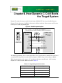
As shown in Figure 1-1, the Rabbit programming cable connects a PC serial port to the programming connector of the target system. Dynamic C runs as an application on the PC, and can cold boot the Rabbitbased target system with no pre-existing program installed in the target.
Figure 1-1. The Rabbit Microprocessor and Dynamic C
PC Hosts Dynamic C
Rabbit Programming
Cable
Level
Conversion
PC Serial
Port
Rabbit
Microprocessor
Target
System
Programming
Connector
Dynamic C programming uses the Rabbit’s serial port A for software development. However, it is possible
with some restrictions for the user’s application to also use port A.
Rabbit 2000 Designer’s Handbook
rabbit.com
1
2
rabbit.com
Introduction
Chapter 2. Rabbit Hardware Design
Overview
Because of the glueless nature of the external interfaces, especially the memory interface, it is easy to
design hardware in a Rabbit-based system. More details on hardware design are given in the Rabbit 2000
Microprocessor User’s Manual.
2.1 Design Conventions
• Include a standard Rabbit programming cable. The standard 10-pin programming connector provides a
connection to serial port A and allows the PC to reset and cold boot the target system.
• Connect a static RAM having at least 32K bytes to the processor using /CS1, /OE1 and /WE1. It is useful if the PC board footprint can also accommodate a RAM large enough to hold all the code anticipated. If a large RAM can be accommodated, software development will go faster. Although code
residing in some flash memory can be debugged, debugging and program download is faster to RAM.
There are also types of flash memory that can be used, but they cannot support debugging.
• Connect a flash memory that is on the approved list and has at least 128K bytes of storage to the processor using /CS0, /OE0 and /WE0. Non-approved memories can be used, but it may be necessary to modify the BIOS. Some systems designed to have their program reloaded by an external agent on each
powerup may not need any flash memory.
• Install a crystal or oscillator with a frequency of 32.768 kHz to drive the battery-backable clock. (Battery-backing is optional, but the clock is used in the cold boot sequence to generate a known baud rate.)
• Install a crystal or oscillator for the main processor clock that is a multiple of 614.4 kHz, or better, a
multiple of 1.8432 MHz. These preferred clock frequencies make possible the generation of sensible
baud rates. If the crystal frequency is a multiple of 614.4 kHz, then the same multiples of the 19,200 bps
baud rate are achievable. Common crystal frequencies to use are 3.6864, 7.3728, 11.0592 or 14.7456
MHz, or double these frequencies.
• Digital I/O line PB1 should not be used in the design if cloning is to be used. (See “BIOS Support for
Program Cloning” on page 45 for more information on cloning.)
2.1.1 Rabbit Programming Connector
The user may be concerned that the requirement for a programming connector places added cost overhead
on the design. The overhead is very small—less than $0.25 for components and board space that could be
eliminated if the programming connector were not made a part of the system.
The programming connector can also be used for a variety of other purposes, including user applications.
A device attached to the programming connector has complete control over the system because it can perform a hardware reset and load new software. If this degree of control is not desired for a particular situation, then certain pins can be left unconnected in the connecting cable, limiting the functionality of the
Rabbit 2000 Designer’s Handbook
rabbit.com
3
connector to serial communications. Rabbit Semiconductor will be developing products and software that
assume the presence of the programming connector.
2.1.2 Memory Chips
Most systems have one static RAM chip and one or two flash memory chips, but more memory chips can
be used when appropriate. Static RAM chips are available in 32K x 8, 64K x 8, 128K x 8, 256K x 8 and
512K x 8 sizes. The 256K x 8 is mainly available in 3 V versions. The other chips are available in 5 V or
3 V versions. Suggested flash memory chips between 128K x 8 and 512K x 8 are given in Chapter 11.,
“Flash Memories.”
Dynamic C and a PC are not necessary for the production programming of flash memory since the flash
memory can be copied from one controller to another by cloning. This is done by connecting the system to
be programmed to the same type of system that is already programmed. This connection is made with a
cloning cable. The cloning cable connects to both programming ports and has a button to start the transfer
of program and an LED to display the progress of the transfer.
2.1.3 Oscillator Crystals
Generally a system will have two oscillator crystals, a 32.768 kHz crystal to drive the battery-backable
timer, and another crystal that has a frequency that is a multiple of 1.8432 MHz or a multiple of 3.6864
MHz. Typical values are 1.8432, 3.6864, 7.3728, 11.0592, 14.7456, 18.432, 25.8048, and 29.4912 MHz.
These crystal frequencies (except 1.8432 MHz) allow generation of standard baud rates up to at least
115,200 bps. The clock frequency can be doubled by an on-chip clock doubler, but the doubler should not
be used to achieve frequencies higher than about 22.1184 MHz on a 5 V system and 14.7456 MHz on a 3.3
V system. A quartz crystal should be used for the 32.768 kHz oscillator. For the main oscillator a ceramic
resonator, accurate to 0.5%, will usually be adequate and less expensive than a quartz crystal.
2.2 Operating Voltages
The operating voltage in Rabbit-based systems will usually be 5 V or 3.3 V, but 2.7 V is also a possibility.
The maximum computation per watt is obtained in the range of 3.0 V to 3.6 V. The highest clock speeds
require 5 V. The maximum clock speed with a 3.3 V supply is 18.9 MHz, but it will usually be convenient
to use a 7.3728 MHz crystal, doubling the frequency to 14.7456 MHz. Good computational performance,
but not the absolute maximum, can be implemented for 5 V systems by using an 11.0592 MHz crystal and
doubling the frequency to 22.1184 MHz. Such a system will operate with 70 ns memories. If the maximum
performance is required, then a 29.4912 MHz crystal or resonator (for a crystal this must be the first overtone, and may need to be special ordered) or a 29.4912 MHz external oscillator can be used. A 29.4912
MHz system will require 55 ns memory access time. A table of timing specification is contained in the
Rabbit 2000 Microprocessor User’s Manual.
4
rabbit.com
Rabbit Hardware Design Overview
2.3 Power Consumption
When minimum power consumption is required, a 3.3 V power supply and a 3.6864 MHz or a 1.8432
MHz crystal will usually be good choices. Such a system can operate at the main 3.6864 MHz or 1.8432
MHz frequency either doubled or divided by 8 (or both). A further reduction in power consumption at the
expense of computing speed can be obtained by adding memory wait states. Operating at 3.6864 MHz,
such a system will draw approximately 11 mA at 3.3 V, not including the power required by the memory.
Approximately 2 mA is used for the oscillator and 9 mA is used for the processor. Reducing the processor
frequency will reduce current proportionally. At 1/4th the frequency or (0.92 MHz) the current consumption will be approximately 4 mA. At 1/8th the frequency, (0.46 MHz) the total power consumption will be
approximately 3 mA, not including the memories. Doubling the frequency to 7.37 MHz will increase the
current to approximately 20 mA.
If the main oscillator is turned off and the microprocessor is operated at 32.768 kHz from the clock oscillator, the current will drop to about 200 µA exclusive of the current required by the memory. The level of
power consumption can be fine-tuned by adding memory wait states, which have the effect of reducing
power consumption. To obtain microampere level power consumption, it is necessary to use auto powerdown flash memories to hold the executing code. Standby power while the system is waiting for an event
can be reduced by executing long strings of multiply zero by zero instructions. Keep in mind that a Rabbit
operating at 3.68 MHz has the compute power of a Z180 microprocessor operating at approximately triple
the clock frequency (11 MHz).
2.4 Through-hole Technology
Most design advice given for the Rabbit assumes the use of surface-mount technology. However, it is possible to use the older through hole technology and develop a Rabbit system. One can use the Rabbit-based
Core Module, a small circuit board with a complete Rabbit core that includes memory and oscillators.
Another possibility is to solder the Rabbit processors by hand to the circuit board. This is not difficult and
is satisfactory for low-production volumes if the right technique is used.
Rabbit 2000 Designer’s Handbook
rabbit.com
5
6
rabbit.com
Rabbit Hardware Design Overview
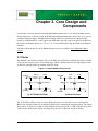
Chapter 3. Core Design and
Components
Core designs can be developed around the Rabbit 2000 microprocessor. A core design includes memory,
the microprocessor, oscillator crystals, the Rabbit standard programming port, and in some cases a power
controller and power supply. Although modern designs usually use at least four-layer printed circuit
boards, two-sided boards are a viable option with the Rabbit, especially if the clock speed is not high and
the design is intended to operate at 2.5 V or 3.3 V—factors which reduce edge speed and electromagnetic
radiation.
Schematics illustrating the use of the Rabbit microprocessor are available at www.rabbitsemiconductor.com.
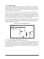
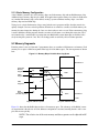
3.1 Clocks
The Rabbit has two built-in oscillators. The 32.768 kHz clock oscillator is needed for the battery-backable
clock (aka, the real-time clock), the watchdog timer, and the cold boot function. The high frequency main
oscillator is generally used to provide the main CPU clock.
Figure 3-1. Rabbit 2000 Oscillator Circuits
XTALA2
330 kW
10 MW CL = 12.5 pF
XTALA1
15 pF
32.768 kHz
15 pF
XTALB2
1 MW
XTALB1
2 kW
CL = 20 pF
33 pF
11.0592 MHz
33 pF
(b) Main Oscillator
(a) 32.768 kHz Oscillator
The 32.768 kHz oscillator is slow to start oscillating after power-on. For this reason a wait loop in the
BIOS waits until this oscillator is oscillating regularly before continuing the startup procedure. The startup
delay may be as much as 5 seconds. Crystals with low series resistance (R < 35 kW) will start faster. If the
clock is battery-backed, there will be no startup delay since the oscillator is already oscillating.
Rabbit 2000 Designer’s Handbook
rabbit.com
7
3.1.1 Low-Power Design
The power consumption is proportional to the clock frequency and to the square of the operating voltage.
Thus, operating at 3.3 V instead of 5 V will reduce the power consumption by a factor of 10.9/25 or 43%
of the power required at 5 V. The clock speed is reduced proportionally to the voltage at the lower operating voltage. Thus the clock speed at 3.3 V will be about 2/3 of the clock speed at 5 V. The operating current is reduced in proportion to operating voltage.
The Rabbit does not have a “standby” mode that some microprocessors have. Instead, the Rabbit has the
ability to switch its clock to the 32.768 kHz oscillator. This is called the sleepy mode. When this is done,
the power consumption is dramatically decreased. The current consumption is often reduced to the region
of 100 µA at this clock speed. The Rabbit executes about 6 instructions per millisecond at this low clock
speed. Generally, when the speed is reduced to this extent, the Rabbit will be in a tight polling loop looking
for an event that will wake it up. The clock speed is increased to wake up the Rabbit.
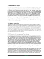
If current consumption by the real-time clock (RTC) is important, the regulator circuit shown in the figure
below will reduce the current consumption by a substantial amount when a 3 V lithium battery is used.
Using this circuit, the battery-backed clock requires less than 25 µA. If the full 3 V is used, the current
consumption will be approximately 70 µA.
Figure 3-2. Clock Oscillator Regulator Circuit
BAT 3 V
1 KW
Safety resistor required
by regulatory agencies
220 KW
battery backup
power
2 MW
0.1 µF
4.3 MW
3.1.2 Conformal Coating of 32.768 kHz Oscillator Circuit
This circuit has low microampere level circuits. To avoid leakage due to moisture and ionic contamination
it is recommended that the oscillator circuit be conformally coated. This is simplified if all components are
kept on the same side of the board as the processor. Feedthroughs that pass through the board and are connected to the oscillator circuit should be covered with solder mask which will serve as a conformal coating
for the back side of the board from the processor. An application note on conformal coating is available
from Rabbit Semiconductor.
8
rabbit.com
Core Design and Components
3.2 Basic Memory Design
Normally /CS0 and /OE0 and /WE0 should be connected to a flash memory that holds the startup code that
executes at address zero. When the processor exits reset with (SMODE1, SMODE0) set to (0,0), it will
attempt to start executing instructions at the start of the memory connected to /CS0, /OE0, and /WE0.
By convention, the basic RAM memory should be connected to /CS1, /OE1, and /WE1. /CS1 has a special
property that makes it the preferred chip select for battery-backed RAM. A bit may be set in the MMIDR
register to force /CS1 to stay enabled (low). This capability can be used to counter a problem encountered
when the chip select line is passed through a device that is used to place the chip in standby by raising
/CS1 when the power is switched over to battery backup. The battery switchover device typically has a
propagation delay that may be 20 ns or more. This is enough to require the insertion of wait states for
RAM access in some cases. By forcing /CS1 low, the propagation delay is not a factor because the RAM
will be always selected and will be controlled by /OE1 and /WE1. If this is done, the RAM will consume
more power while not battery-backed than it would if it were run with dynamic chip select and a wait state.
If this special feature is used to speed up access time for battery backed RAM then no other memory chips
should be connected to /OE1 and /WE1.
3.2.1 Memory Access Time
The memory access time required depends on the clock speed and the capacitive loading of the address
and data lines. Wait states can be specified by programming to accommodate slow memories for a given
clock speed. Wait states should be avoided with memory that holds programs because there is a significant
slowing of the execution speed. Wait states are far more important in the instruction memory than in the
data memory since the great majority of accesses are instruction fetches. Going from 0 to 1 wait states is
about the same as reducing the clock speed by 30%. Going from 0 to 2 wait states is worth approximately
a 45% reduction in clock speed. A table of memory access times required for various clock speeds is given
in the Rabbit 2000 Microprocessor User’s Manual.
3.2.2 Precautions for Unprogrammed Flash Memory
If a Rabbit-based system is powered up and released from reset when not in one of the cold boot modes,
the processor attempts to begin execution by reading from address zero of the memory attached to /CS0,
/OE0, and /WE0. If this memory is an unprogrammed or improperly programmed flash memory, there is a
danger that the memory could be destroyed if the write security feature of the flash memory is disabled.
Flash memories have a write security feature that inhibits starting write cycles unless a special code is first
stored to the memory. For example, Atmel flash memories use the bytes AAh, 55h, and A0h stored to
addresses AAAAh or 5555h in a particular sequence. Any write executed that is not prefixed by this
sequence will be ignored. If the memory has write protection disabled, and execution starts, it is possible
that an endless loop that includes a write to memory will establish itself. Since the flash memory wears out
after a few hundred thousand writes, the memory could be damaged in a short period of time by such a
loop. Unfortunately, flash memory is shipped from the factory with the protection feature disabled to
accommodate obsolete memory programmers.
The solution to this problem is to order the memory with the write protection enabled, or to enable it with a
flash programming system. Then the memory will be safe if it is soldered into the Rabbit system. If an
unsafe memory is soldered into a system, then the memory can be powered up with the programming cable
connected, and a sequence can be sent using the cold boot procedure to enable the write protection. Compiling any Dynamic C program to the flash will make the memory safe. If this is not convenient, tester
Rabbit 2000 Designer’s Handbook
rabbit.com
9
software can make the memory safe by sending a byte sequence over the programming connection serial
link.
The following example shows a program that can be downloaded via the cold boot protocol to make a
Atmel AT29C010A 128K x 8 flash memory safe. In this case, the RAM connected to /CS1 is used to hold
a program starting at address zero. The flash memory is mapped into the data segment starting at address
1000h for access to the start of the flash memory.
; Before storing this program, the RAM is mapped to the first quadrant.
; The program resides at address zero in RAM.
; NOTE: this program has not been tested
ld a,0e1h
ioi ld (13h),a
ld a,3fh
ioi ld(12h),a
ld a,0
ld (15h),a
ld a,0aah
ld (5555h+1000h),a
ld a,55h
ld (2AAAh+1000h),a
ld a,0a0h
ld (5555h+1000h),a
ld hl,1000h
ld (hl),0c3h
inc hl
ld (hl),00h
inc hl
ld (hl),00h
jr *
; 3e e1 segsize reg
; d3 32 13 00 data seg starts at 1000h
; 3e 3f dataseg reg
; d3 32 12 00 set data seg base of flash to 1000h
; 3e 00 for MB1CR memory bank reg for flash on CS0
; 32 15 00 bank 1 reads flash starting at 256k
; 3e aa
; 32 55 65 first byte of unlock code
; 3e 55
; 32 aa 3a 2nd byte of unlock code
; 3e a0
; 32 55 65 3rd byte of unlock code
; 21 00 10 point to start of flash memory
; 36 c3 jump op code
; 23
; 36 00 zero
; 23
; 36 00 zero
; 18 fe end with endless loop
This code can be sent by means of a sequence of triplets via the serial port.
80 14 01
00 00 3e
00 01 e1
00 02 d3
00 03 32
00 04 12
00 05 00
; continue code above here
00 2b 18
00 2c fe
80 24 80
; I/O write 01 to 0000 MB0CR select cs1- map RAM to Q1
; write to memory address 0
; last instruction
; last byte
; start execution of program at zero
The program will execute within about 10 ms.
10
rabbit.com
Core Design and Components
3.3 PC Board Layout and Memory Line Permutation
To use the PC board real estate efficiently, it is recommended that the address and data lines to memory be
permuted to minimize the use of PC board resources. By permuting the lines, the need to have lines cross
over each other on the PC board is reduced, saving feed-through’s and space.
For static RAM, address and data lines can be permuted freely, meaning that the address lines from the
processor can be connected in any order to the address lines of the RAM, and the same applies for the data
lines. For example, if the RAM has 15 address lines and 8 data lines, it makes no difference if A15 from
the processor connects to A8 on the RAM and vice versa. Similarly D8 on the processor could connect to
D3 on the RAM. The only restriction is that all 8 processor data lines must connect to the 8 RAM data
lines. If several different types of RAM can be accommodated in the same PC board footprint, then the
upper address lines that are unused if a smaller RAM is installed must be kept in order. For example, if the
same footprint can accept either a 128K x 8 RAM with 17 address lines or a 512K x 8 RAM with 19
address lines, then address lines A18 and A19 can be interchanged with each other, but not exchanged with
A0–A17.
Permuting lines does make a difference with flash memory. If the memory is socketed and it is intended to
program the memory off the board, then it is probably best to keep the address and data lines in their natural order. However, since the flash can be programmed in the circuit using the Rabbit programming port, it
is expected that most designers will solder the flash memory directly to the board in an unprogrammed
state. In this case, the permeation of data and address lines must still be taken into account because flash
memory requires the use of a special unlock code that removes write protection. The unlock operation
involves a special sequence of reads and writes accessing special addresses and writing the unlock codes.
Another consideration is that the flash memory may be divided into sectors. An entire sector must be written to modify the memory. Small-sector memories are divided into 1024 sectors. If the largest flash memory that is usable in a particular design is 512K, the largest sector size is 512 bytes. If the smallest memory
used is 128K, then the smallest sector is 128 bytes. In order that the sector can be contiguous for all possible types of memory, the lower 7 address lines (A0…A6) should be permuted as a group. Address lines A7
and A8 should not be permuted at all if it is desirable to keep the larger sectors contiguous. The upper 10
address lines can be permuted as a separate group. The special memory chip addresses 05555h and
0AAAAh must be accessed as part of the unlock sequence. These addresses use only the first 16 address
lines and have the odd and even numbered bits the same. The unlock codes use the numbers 55h, AAh or
A0h.
Permuting data or address lines with flash memory should probably be avoided in practical systems.
Rabbit 2000 Designer’s Handbook
rabbit.com
11
3.4 PC Board Layout and Electromagnetic Interference
Most design failures are related to the layout of the printed circuit board (PCB). A good layout results
when the effects of electromagnetic interference (EMI) are considered. EMI refers to unintentional radiation from the circuit board that might cause interference with other devices, mainly television sets. If the
PCB layout meets EMI regulations, it will probably be otherwise electrically sound.
3.4.1 EMI Regulations
The Federal Communications Commission (FCC) regulates EMI standards in the United States. Their
jurisdiction is all 50 states, the District of Columbia, and U.S. possessions. The European Union (EU) regulates EMI standards in Europe by means of a CE Marking that acts as a product’s passport in the European market. The actual CE Marking is the letters "CE," an abbreviation of a French phrase "Conformite
Europeene."
These regulations specify the maximum radiation measured in units of field strength (microvolts / meter)
at a standard distance, usually 3 meters. The field strength must be measured using a particular type of filter (120 kHz wide) and a particular type of peak detection (quasi-peak). With Rabbit-based systems, the
radiation will generally be pure tones at harmonics of the clock speed. This makes it unnecessary to use a
special filter or quasi peak detection except for final verification measurements.
3.4.1.1 EMI Measuring Devices
The measurements are performed using a spectrum analyzer coupled to a calibrated antenna. The equipment needed to perform these tests may cost $25,000 or more. Many designers will use outside laboratories to perform the tests. There is not necessarily a legal requirement to perform the tests. It depends on the
type of equipment and its intended use. For example, FCC regulations in the USA exempt industrial equipment.
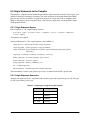
3.4.1.2 Classes For EMI Testing
FCC computer regulations divide equipment into two classes.
CLASS A
CLASS B
Computer equipment meant for office use: business Computer equipment meant for home use, where a
machines, office computers
television is likely to be nearby.
Less restrictive emissions requirement: less than 50
More restrictive emissions requirement: 40 dBuV/M
dB/uV/M at 3 meters (50 dB relative to 1 microvolt
or 100 uV/M.
per meter or 300 microvolts / meter).
Note that for field strength, 20 dB is a factor of 10 and 6 dB is a factor of 2. Field strength declines
inversely with distance, so at 10 meters the field strength for the same device will be about 3/10ths as large
as at 3 meters which is approximately 10 dB less. (20 dB is a factor of 10, 10 dB is a factor of the square
root of 10 or 1/3.16 = 3.16/10.) These limits apply in the range of 30-230 MHz for the more restrictive CE
test. Above 230 MHz the limit is 7 dB higher. Although the test range goes to 1 GHz, with Rabbit-based
systems there will rarely be any concern above 300 MHz.
With a Rabbit-based system it is easy to meet the Class B limits if proper PCB layout precautions are
observed. At Rabbit Semiconductor, our target is to beat the Class B limit by 10 dB.
12
rabbit.com
Core Design and Components
3.4.2 Layout and Decoupling for Low EMI
Generally you should design with a 4 (or more) layer printed circuit board. The cost of a 4-layer board as
compared to a 2-layer board is about 30% more per square inch and generally well worth it. Although we
have not attempted it, a 2-layer design would probably work for lower clock frequencies if the ground and
power nets are well gridded for power distribution (see Section 3.4.2.5 on page 18).
Usually a 4-layer printed circuit board has a ground plane and a power plane located as the two inner layers and connect layers on the top and bottom layers. Components may be mounted on only one side or on
both sides. A 6-layer board places the ground and power layers as the middle two layers and then has two
routing layers both above and below. Adjacent routing layers run traces at right angles to minimize coupling between signal traces. Sometimes the ground and power layers are placed on the outside of the
boards, but this makes debugging more difficult and compromises the layers more since they have to be
cut up for the component footprints.
3.4.2.1 EMI Sources
Most EMI comes from signals that are strictly regular. The main sources are the crystal oscillator, the lines
emanating from the Rabbit chip that are affected by the internal clocking of the chip, and the actual clock
or clock/2 if it is run around the printed circuit board. Address and data lines generate less EMI because
there is no regular frequency on these lines since the bus cycles vary in length, shifting the signal phase
constantly. A0 is the hottest address line since it is varying most rapidly and also has a stronger drive than
the other address lines.
A square wave has harmonics at odd frequencies that decline in amplitude proportional to 1/f. A small
wire that acts as an antenna radiates more the higher the frequency of excitation. The effectiveness as an
antenna increases proportional to frequency. These two effects approximately cancel, resulting in an
approximately flat spectrum for a typical printed circuit board. For example, without taking precautions, it
would not be unusual to have a problem with the 7th harmonic, or 154.7 MHz when the Rabbit clock is
22.1 MHz. Above approximately 300 MHz, the edges are not fast enough to generate strong harmonics for
typical Rabbit systems.
Rabbit 2000 Designer’s Handbook
rabbit.com
13
3.4.2.2 Clock Signal Pin 1
Pin 1 of the Rabbit can be programmed to output the internal clock or the internal clock divided by 2. The
Rabbit BIOS automatically disables this pin, starting with Dynamic C 7.01. To minimize EMI, avoid using
this pin as a clock output. Most Rabbit designs do not need to explicitly use the clock output pin. However,
in cases that require a clock, use clock/2 if possible. Also, a series resistor can (and should) be placed in
the clock line to slow down the rise and fall times, which will reduce radiation at higher harmonics of the
frequency. Place the resistor, which might be around 1 K ohms, as close to pin 1 as possible. The capacitive load of whatever the clock line is connected to, along with the resistor, creates an RC time constant
that slows the edge. If the capacitive load is larger, a smaller resistor is needed and vice versa.
The clock line should be kept as short as possible, and run over a ground plane—or even better between
two ground planes. It should be positioned well away from other traces, especially traces running parallel
to it for any distance. Coupling to a parallel trace is greater the faster the edges. If you run parallel ground
traces or a ground trace above the clock line then the parallel ground traces should be connected with very
low inductance connections to the ground plane. This is done by using many feedthroughs.
Figure 3-3. Many feedthroughs provide very low inductance connections between parallel ground
traces and a ground plane
Pin1
Clk
1 kW
Feedthroughs to
Ground Plane
Parallel
Ground Traces
14
rabbit.com
Core Design and Components
3.4.2.3 High Frequency Oscillator Circuit
The Rabbit’s oscillator circuit typically runs at 11.05 MHz for a 22.1 MHz internal clock. The internal
clock doubler is used to double the clock frequency. If the clock doubler is not used then the external oscillator circuit runs at the full internal clock frequency, resulting in more radiation from the external circuit
due to its higher frequency. In either case there should not be excessive radiation from this circuit if layout
guidelines are followed.
The main objective is to keep the loop area of the circuit small so as to avoid coupling the clock to other
lines and because current circulating in a loop acts as an antenna. The part of the circuit most susceptible to
radiation is the trace from pin 91 to the 2 kΩ resistor (see Figure below). The remainder of the circuit has
the edges slowed by the 2 kΩ resistor.
The low frequency of the 32.768 kHz clock causes no radiation.
Figure 3-4. Loop area of the circuit should be kept small.
XTALB2(91)
1 MW
XTALB1(90)
Rabbit 2000 Designer’s Handbook
2 kW
Current
Loop
33 pF
Crystal (typ. 11.05 MHz)
20 pF
33 pF
rabbit.com
15
CL1
Rabbit 2000
Rp
Copper pour connected to ground plane
Y1
Figure 3-5. Avoid coupling the clock to other lines.
VSS
XTALB1
XTALB2
CL2
Rs
VDD
Table 3-1: High Speed Crystal Oscillator
Component
Name
16
Component Description
Value
CL1
Input Cap
33 pF
CL2
Output Cap
33 pF
Rp
Bias Resistor
1 MΩ
Rs
Current Limiting Series Resistor
2 KΩ
Y1
High speed oscillator
CL=20 pF
rabbit.com
Core Design and Components
3.4.2.4 Processor Decoupling
The internal clock of the processor is routed throughout the silicon die. On the rising edge of the clock all
the flip flops on the die are clocked within a nanosecond or so of each other, resulting in large current
flows through the ground and power pins. The current surge is mainly due to the capacitance driven by the
clock and by flip flops changing their state on the clock. The connections from the ground and power pins
to the die have inductance, as do the connections within the die. The ground and power on the die will
bounce up and down at the clock frequency and this will be coupled to all the other I/O lines that are
clamped to power or ground by transistors. To minimize this bouncing a low impedance path from the
pairs of ground and power pins to decoupling capacitors should be provided.
The Rabbit has 6 power and 6 ground pins. Of the six power pins, five reside on the main power grid and
are used to power the CPU, peripherals and the I/O. The other one, pin 42, resides on a separate power net
to supply the battery-backed clock. The ground pins are all tied to the common ground network.
To minimize EMI, connect all power pins as directly as possible to a ground plane running under the processor without large slots or non-metal areas in the plane. A low inductance connection is obtained by a
short and wide trace leading to the feedthrough to the ground plane. A pair of feedthroughs has less inductance than a single feedthrough. The power pins should be connected by a low inductance path to the
power plane, or if there is no power plane, to a decoupling capacitor.
For capacitors immediately adjacent to the processor, use 10 nF decoupling capacitors (.01 µF). Larger
capacitors have too much inductance, resulting in excessive harmonics above 100 MHz.
Figure 3-6. Decoupling capacitor placement and layout.
Rabbit 2000
VSS
VDD
Decoupling of pin 42 (Vbat) is not critical since relatively small currents flow through this pin.
Rabbit 2000 Designer’s Handbook
rabbit.com
17
3.4.2.5 Elimination of Power Plane
If the power plane is eliminated or extensively slotted to accommodate routed traces, decoupling and
power distribution becomes more critical. The key is to maintain a low inductance connection from “hot”
package power pins to a decoupling capacitor. Also, keep the inductance between widely separated parts
of the power net as low as possible. Gridding the net in a cross connect pattern will lower inductance
between points, as will wider traces. The procedure is to use a grid and then use wide traces from grid
intersections to the decoupling capacitors or packages.
Figure 3-7. Power Distribution Grid
Wide
Trace
Decoupling
Capacitor
VDD
18
rabbit.com
to VSS
(GND)
Core Design and Components
Chapter 4. How Dynamic C Cold Boots
the Target System
Dynamic C assumes that target controller boards using the Rabbit CPU have no pre-installed firmware.
Dynamic C takes advantage of the Rabbit’s bootstrap (cold boot) mode that allows memory and I/O writes
to take place over the programming port.
Figure 4-1. Rabbit Programming Port
Circuit Board with Rabbit 2000 Processor
6
7
9
RXA
8
GND
10
CLKA
Vcc
Programming
Header Pinout
/RESET
TXA
n.c.
STATUS
SMODE0
51
2
GND
3
94
4
+5 V
5
37
6
54
7
8
38
9
36
10
35
~50 kW
SMODE1
1
~5 kW
4
5
RABBIT 2000
RXA
VSS
CLKA
VDD
/RESET
TXA
STATUS
SMODE0
SMODE1
~50 kW
3
Vcc
Programming
Header
~50 kW
2
~50 kW
1
The Rabbit programming cable is a smart cable with an active circuit board in its middle. The circuit board
converts RS-232 voltage levels used by the PC serial port to CMOS voltage levels used by the Rabbit.
When the programming cable connects a PC serial port to the target controller board, the PC running
Dynamic C is connected to the Rabbit as shown in Table 4-1.
Table 4-1. Programming Port Connections
PC Serial Port Signal
Rabbit Signal
DTR (output)
/RESET (input, reset system)
DSR (input)
STATUS (gen purpose output)
TX (serial output)
RXA (serial input, chan A)
RX (serial input)
TXA (serial output, chan A)
Rabbit 2000 Designer’s Handbook
rabbit.com
19
The programming cable includes an RS-232 to CMOS signal level converter circuit. The level converter is
powered from the +5 V or +3.3 V power supply voltage present on the Rabbit programming connector (see
Figure 4-1). Plugging the programming cable into the Rabbit programming connector results in pulling the
Rabbit SMODE0, SMODE1 (startup mode) lines high. This causes the Rabbit to enter the cold boot mode
after reset.
Dynamic C can cold boot the Rabbit-based target system with no pre-existing program installed in the target. The flash memory on the target system can be blank or it may contain any data. The cold boot capability permits the use of soldered-in flash memory on the target. Soldered-in memory eliminates sockets, boot
blocks and prom programming devices. However, it is important that the flash memory have its software
data protection enabled before it is soldered in.
4.1 How the Cold Boot Mode Works In Detail
The microprocessor starts executing a 12-byte program contained in an internal ROM. The program contains the following code.
; origin zero
00 ld l,n
02
04
06
08
09
10
ioi ld d,(hl)
ioi ld e,(hl)
ioi ld a,(hl)
ioi or nop
ld (de),A
jr 0
;
;
;
;
;
;
;
;
n=0c0h for serial port A
n=020h for parallel (slave port)
get address most significant byte
get least significant byte
get data (h is ignored)
if D(7)==1 ioi, else nop
store in memory or I/O
jump back to zero
; note wait states inserted at bytes 3, 5 and 7 waiting
; for serial port or parallel port ready
The contents of the boot ROM vary depending on the settings of the pins SMODE0 and SMODE1 and on
the contents of register D bit 7 which determines if the store is to be an I/O store or a data store. If the boot
is terminated by storing 0x80 to I/O register 0x24, then when the boot program reaches address zero the
boot mode is disabled and instruction fetching resumes at address zero.
Wait states are automatically inserted during the fetching of bytes 3, 5 and 7 in order to wait for the serial
or parallel port ready. The wait states continue indefinitely until the serial port is ready. This will cause the
processor to be in the middle of an instruction fetch until the next character is ready. While the processor is
in this state, the chip select, but not the output enable, will be enabled if the memory mapping registers are
such as to normally enable the chip select for the boot ROM address. The chip select will stay low for
extended periods while the processor is waiting for the serial or parallel port data to be ready. Additionally,
the chip select will go low when a write is performed to an I/O address if the address is such as to enable
that chip select if it were a write to a memory address.
20
rabbit.com
How Dynamic C Cold Boots the Target System
4.2 Program Loading Process Overview
The program loading process described here is current through Dynamic C version 7.06.
On start up, Dynamic C first uses the PC’s DTR line on the serial port to assert the Rabbit Reset line and
put the processor in cold boot mode. Next, Dynamic C uses a four stage process to load a user program:
1. Load an initial loader (cold loader) via triplets sent at 2400 baud from the PC to a target in cold boot
mode.
2. Run the initial loader and load a secondary loader (pilot BIOS) at 19200 or 57000 baud, depending on
the version of Dynamic C.
3. Run the secondary loader and load the BIOS (as Dynamic C compiles it).
4. Run the BIOS and load the user program at 115200 baud (after Dynamic C compiles it to a file).
4.2.1 Program Loading Process Details
When Dynamic C starts, the following sequence of events takes place:
1. The serial port is opened with the DTR line high, closed, then reopened with the DTR line low at 2400
baud. This pulses the reset line on the target low (the programming cable inverts the DTR line) and prepares the PC to send triplets.
2. A group of triplets defined in the file COLDLOAD.BIN consisting of 2 address bytes and a data byte
are sent to the target. The first few bytes sent are sent to I/O addresses to set up the memory mapping
unit (MMU) and the memory interface unit (MIU) and do system initialization. The MMU is set up so
that RAM is mapped to 0x00000, and flash is mapped to 0x80000.
3. The remaining triplets place a small initial loader program at memory location 0x00000. The last triplet
sent is 0x80, 0x24, 0x80, which tells the CPU to ignore the SMODE pins and start running code at
address 0x00000.
4. The PC now bumps the baud rate on the serial port being used to 19200 or 57000 baud, depending on
the version of Dynamic C.
5. The primary loader measures the crystal speed to determine what divisor is needed to set a baud rate of
19200 (or 57600). The divisor is stored at address 0x4002 for later use by the BIOS, and the programming port is set up to be a 19200 (or 57600) baud serial port.
6. The program enters a loop where it receives a fixed number of bytes which compose a secondary loader
program (pilot.bin sent by the PC) and writes those bytes to memory location 0x4100. After all of
the bytes are received, program execution jumps to 0x4100.
7. The secondary loader does a wrap-around test to determine how much RAM is available, and reads the
flash ID. This information is made available for transmittal to Dynamic C when requested.
8. The secondary loader now enters a finite state machine (FSM) that is used to implement the Dynamic
C/Target Communications protocol. Dynamic C compiles the core of the regular BIOS and sends it to
the target at address 0x00000 which is still mapped to RAM. Note that this requires that the BIOS core
be 0x4000 or less in size.
Rabbit 2000 Designer’s Handbook
rabbit.com
21
9. The FSM checks the memory location 0x4001 (previously set to zero) after receiving each byte. When
the compilation and loading to RAM of the BIOS is complete, Dynamic C signals the target that it is
time to run the BIOS by sending a one to 0x4001.
10. The BIOS runs some initialization code including setting up the serial port for 115200 baud, setting up
serial interrupts and starting a new FSM.
11. The BIOS code modifies a jump instruction at the beginning of the program so that the next time it
runs, it will skip step 12. It also modifies a byte near the beginning of the program where it stores the
baud rate divider to achieve 19200 baud. This constant is used by the serial communications initialization library functions to compute baud rate dividers.
12. The BIOS copies itself to flash at 0x80000, and switches the mapping of flash and RAM so that RAM
is at 0x80000 and flash is at 0x00000. As soon as this remapping is done, the BIOS’ execution of
instructions begins happening in flash.
13. Dynamic C is now ready to compile a user program. When the user compiles his program to the target,
it is first written to a file, then the file is loaded to the target using the BIOS’ FSM. The file is used as an
intermediate step because fix-ups are done after the compilation is complete and all unknown addresses
are resolved. The fix-ups would cause extra wear on the flash if done straight to the flash.
14. When the program is fully loaded, Dynamic C sets a breakpoint at the beginning of main and runs the
program up to the breakpoint. The board has been programmed, and Dynamic C is now in debug mode.
15. If the programming cable is removed and the target board is reset, the user’s program will start running
automatically because the BIOS will check the SMODE pins to determine whether to run the user
application or enter the debug kernel.
22
rabbit.com
How Dynamic C Cold Boots the Target System
Chapter 5. Rabbit Memory Organization
The Rabbit architecture is derived from the original Z80 microprocessor. The original Z80 instruction set
used 16-bit addresses to address a 64K memory space. All code and data had to fit in this 64K space. The
Rabbit adopts a scheme similar to that used by the Z180 to expand the available memory space. The 64K
space is divided into zones and a memory mapping unit or MMU maps each zone to a block in a larger
memory; the larger memory is 1MB in the case of the Z180 or the Rabbit 2000. The zones are effectively
windows to the larger memory. The view from the window can be adjusted so that the window looks at different blocks in the larger memory. Figure 5-1 on page 24 shows the memory mapping schematically.
5.1 Physical Memory
The Rabbit has a 1MB physical memory space. In special circumstances more than 1MB of memory can
be installed and accessed using auxiliary memory mapping schemes. Typical Rabbit systems have two
types of physical memory: flash memory and static RAM memory. Flash memory follows a write-once-ina-while and read-frequently model. Depending on the particular type of flash used, the flash memory will
wear out after it has been written approximately 10,000 to 100,000 times.
5.1.1 Flash Memory
Flash memory in a Rabbit-based system may be small-sector type or large-sector type. Small-sector memory typically has sectors of 128 to 1024 bytes. Individual sectors may be separately erased and written. In
large-sector memory the sectors are often 16K or 64K or more. Small-sector memory provides better support for program development and debugging, and large-sector memory is less expensive and has faster
access time. The best solution will usually be to lay out a design to accept several different types of flash
memory, including the flexible small-sector memories and the fast large-sector memories.
At the present time development support for programs tested in flash memory is confined to flash memories with small sectors. If larger sectors are used, the code must be debugged in RAM and then loaded to
flash. Large-sector flash is desirable for the better access time and power consumption specifications that
are available. Dynamic C is being modified to handle large sector flash at the time of this writing.
5.1.2 SRAM
Static RAM memory may or may not be battery-backed. If it is battery-backed it retains its data when
power is off. Static RAM chips typically used for Rabbit systems are 32K, 64K, 128K, 256K, or 512K.
When the memory is battery-backed, power is supplied at 2 V to 3 V from a backup battery. The shutdown
circuitry must keep the chip select line high while preserving memory contents with battery power.
Rabbit 2000 Designer’s Handbook
rabbit.com
23
5.1.3 Basic Memory Configuration
A basic Rabbit system has two static memory chips: one flash memory chip and one RAM memory chip.
Additional static memory chips may be added. If an application requires storing a lot of data in flash memory, another flash memory chip can be added, creating a system with three memory chips—two flash
memory chips and one RAM chip.
Trying to use a single flash memory chip to store both the user’s program and live data that must be frequently changed can create software problems. When data are written to a small-sector flash memory, the
memory becomes inoperative during the 5 ms or so that it takes to write a sector. If the same memory chip
is used to hold data and the program, then the execution of code must cease during this write time. The 5
ms is timed out by a small routine executing from root RAM while system interrupts are disabled, effectively freezing the system for 5 ms. The 5 ms lockup period can seriously affect real-time operation.
5.2 Memory Segments
From the point of view of a Dynamic C programmer, there are a number of different uses of memory. Each
memory use occupies a different segment in the logical 16-bit address space. The four segments are shown
here:
Figure 5-1. Memory Map of 16-bit Addressing Space
1 MB
Quandrant 3
64 KB
Extended
Memory
Segment
56 KB
Stack
Segment
RAM
Quadrant 2
52 KB
Data
Segment
Quadrant 1
Base
Segment
Flash
(aka Root Segment)
0 KB
Logical Address Space
Quadrant 0
0 KB
Physical Address Space
Figure 5-1 shows that the Rabbit does not have a flat memory space. The advantage of the Rabbit’s memory organization is that the use of 16-bit addresses and pointers is retained, ensuring that the code is compact and executes quickly.
NOTE: The relative size of the root memory and data segments can be adjusted in 4K
steps.
24
rabbit.com
Rabbit Memory Organization
5.2.1 Definitions
Extended Code: Instructions addressed in the extended memory segment.
Extended Constants: C constants addressed in the extended memory segment. They are mixed together
with the extended code.
Extended Memory: Logical addresses above 0xDFFF; also known as xmem.
Extended RAM: RAM not used for root variables or stack. Extended memory in RAM may be used for
large buffers to save root RAM space. The function xalloc() allocates space in extended RAM memory.
Root Code: Instructions addressed in the root memory segment.
Root Constants: C constants, such as quoted strings or data tables, addressed in the root memory segment.
Root Memory: Logical addresses below 0xE000.
Root Variables: C variables, including structures and arrays that are not initialized to a fixed value, are
addressed in the data segment.
5.2.2 The Root Memory Segment
The root memory segment has a typical size of 24K. The larger the root memory segment, the smaller the
data segment and vice-versa. Root memory segment address zero is always mapped to 20-bit address zero.
Usually the root memory segment is mapped to flash memory since root code and root constants do not
change except when the system is reprogrammed. It may be mapped to RAM for debugging, or to take
advantage of the faster access time offered by RAM.
The root memory segment holds a mixture of code and constants. C functions or assembly language programs that are compiled to the root memory segment are interspersed with data constants. Data constants
are inserted between blocks of code. Data constants defined inside a C function are put before the end of
the code belonging to the function. Data constants defined outside of C functions are stored as encountered
in the source code.
Except in small programs, the bulk of the code is executed using the xmem segment. But code in the root
memory segment operates slightly faster, also the root memory segment has special properties that make it
better for some types of code.
5.2.2.1 Types of Code Best-Suited for the Root Memory Segment
• Short subroutines of about 20 instructions or less that are called frequently will use significantly
less execution time if placed in root memory because of the faster calling linkage for 16-bit versus 20bit addresses. For a call and return, 20 clocks are used compared to 32 clocks.
• Interrupt routines. Interrupts use 16-bit addressing so the entry to an interrupt routine must be in root.
• The BIOS core. The initialization code of the BIOS must be at the start of the root memory segment.
Rabbit 2000 Designer’s Handbook
rabbit.com
25
5.2.3 The Data Segment
The data segment is mapped to RAM and contains C variables. Typically it starts at 8K or above and ends
at 52K (0xCFFF). Data allocation starts at or near the top and proceeds in a downward direction. It is also
possible to place executable code in the data segment if it is copied from flash to the data segment. This
can be desirable for code that is self modifying, code to implement debugging aids or code that controls
write to the flash memory and cannot execute from flash. In some cases RAM may require fewer wait
states so code executes faster if copied to RAM.
5.2.4 The Stack Segment
The stack segment normally is from 52K to 56K (0xD000-0xDFFF). It is always mapped to RAM and
holds the system stack. Multiple stacks may be implemented by defining several stacks in the 4k space or
by remapping the 4K space to different locations in physical RAM memory, or by using both approaches.
For example, if 16 stacks of 1k length are needed then 4 stacks can be placed in each 4K mapping and 4
different mappings for the window can be used.
5.2.5 The Extended Memory Segment
This 8K segment from 56K to 64K (0xE000-0xFFFF) is used to execute extended code and it is also used
by routines that manipulate data located in extended memory. While executing code the mapping is shifted
by 4K each time the code passes the 60K point. Up to a megabyte of code can be efficiently executed by
moving the mapping of the 8K window using special instructions (long call, long jump and long return)
that are designed for this purpose. This uses up only 8K of the 16-bit addressing space.
5.3 How The Compiler Compiles to Memory
The compiler generates code for root code, root constants, extended code and extended constants. It allocates space for data variables, but, except for constants, does not generate data to be stored in memory.
Any initialization of variables must be accomplished by code since the compiler is not present when the
program starts in the field.
5.3.1 Placement of Code in Memory
Code may be placed in either extended memory or root memory. Functions execute at the same speed, but
calls to functions in root memory are slightly more efficient than calls to functions in extended memory.
In all but the smallest programs, most of the code is compiled to extended memory. Since root constants
share the memory space needed for root code, as the memory needed for root constants increases, the
amount of code that can be stored in root memory decreases, and code must be moved to extended memory.
26
rabbit.com
Rabbit Memory Organization
5.3.2 Paged Access in Extended Memory
The code in extended memory executes in the 8K window from 0xE000 to 0xFFFF. This 8K window uses
paged access. Instructions that use 16-bit addressing can jump within the page and also outside of the page
to the remainder of the 64K logical space. Special instructions, particularly lcall, ljp, and lret, are
used to access code outside of the 8K window. When one of these transfer-of-control instructions is executed, both the address and the view through the 8K window change, allowing transfer to any instruction
in the 1M physical memory space. The 8-bit XPC register controls which of two consecutive 4K pages
aligns with the 8K window (there are 256 pages). The 16-bit PC controls the address of the instruction,
usually in the region 0xE000 to 0xFFFF. The advantage of paged access is that most instructions continue
to use 16-bit addressing. Only when a page change is needed does a 20-bit transfer of control need to be
made.
As the compiler compiles code in the extended code window, it checks at opportune times to see if the
code has passed the midpoint of the window or 0xF000. When the code passes 0xF000, the compiler slides
the window down by 4K so that the code at 0xF000+x becomes resident at 0xE000+x. This automatic paging results in the code being divided into segments that are typically 4K long, but which can be very short
or as long as 8K. Transfer of control within each segment can be accomplished by 16-bit addressing.
Between segments, 20-bit addressing is required.
Rabbit 2000 Designer’s Handbook
rabbit.com
27
28
rabbit.com
Rabbit Memory Organization
Chapter 6. The Rabbit BIOS
When Dynamic C compiles a user’s program to a target board, the BIOS (Basic Input-Output System) is
compiled first, as an integral part of the user’s program. The BIOS is a separate program file that contains
the code needed to interface with Dynamic C. It also normally contains a software interface to the user’s
particular hardware. Certain drivers in the Dynamic C libraries require BIOS routines to perform tasks that
are hardware-dependent.The BIOS also:
• Provides a variety of low-level services for the user’s program.
• Takes care of microprocessor system initialization.
• Provides the communications services required by Dynamic C for downloading code and performing
debugging services such as setting breakpoints or examining data variables.
• Defines the setup of memory.
A single, general-purpose BIOS is supplied with Dynamic C for the Rabbit. This BIOS will allow you to
boot Dynamic C on any Rabbit-based system that follows the basic design rules needed to support
Dynamic C. The BIOS requires both a flash memory and a 32K or larger RAM or just a 128K RAM for it
to be possible to compile and run Dynamic C programs. If the user uses a flash memory from the list of
flash memories that are already supported by the BIOS, the task will be simplified. If the flash memory
chip is not already supported, the user will have to write a driver to perform the write operation on the
flash memory. This is not difficult provided that a system with 128K of RAM and the flash memory to be
used is available for testing.
An existing BIOS can be used as a skeleton BIOS to create a new BIOS. Frequently it will only be necessary to change #define statements at the beginning of the BIOS. In this case it is unnecessary for the
user to understand or work out the details of the memory setup and other processor initialization.
Rabbit 2000 Designer’s Handbook
rabbit.com
29
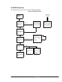
6.1 Startup Conditions Set Up By the BIOS
The BIOS sets up initial values for the following registers by means of code and declarations.
• The four memory bank control registers —MB0CR, MB1CR, MB2CR, and MB3CR—are 8-bit registers,
each associated with one quadrant of the 1M memory space. Each register determines which memory
chip will be mapped into its quadrant, how many wait states will be used for accessing that memory
chip, and whether the memory chip will be write protected.
• The STACKSEG register is an 8-bit register that determines the location of the stack segment in the 1M
memory.
• The DATASEG register is an 8-bit register that determines the location of the data segment in the 1M
memory, normally the location of the data variable space.
• The SEGSIZE register is an 8-bit register holding two 4-bit registers. Together the registers determine
the relative size of the base segment, data segment and stack segment in the 64K root space.
• The MMIDR register is an 8-bit register used to force /CS1 to be always enabled or not. Having /CS1
always enabled reduces power consumption.
• The XPC register is used to address extended memory. Normally the user’s code frequently changes this
register. The BIOS sets the initial value.
• The SP register is the system stack pointer. It is frequently changed by the user’s code. The BIOS sets
up an initial value.
All together there are 11 MMU and MIU registers that are set up by the BIOS. These registers determine
all aspects of the hardware setup of the memory.
In addition, a number of origin declarations are made in the BIOS to tell the Dynamic C compiler where to
place different types of code and data. The compiler maintains a number of assembly counters that it uses
to place or allocate root code, extended code, data constants, data variables, and extended data variables.
Each of these counters has a starting location and a block size.
30
rabbit.com
The Rabbit BIOS
6.2 BIOS Flowchart
The following flowchart summarizes the functionality of the BIOS:
Figure 6-1. BIOS Flowchart
Application
Program
Start at
address 0
Initializing
BIOS flag?
Yes
Copy BIOS to
flash. Clear flag
in source code.
BIOS services
for user application program.
No
Setup memory
control and
basic BIOS services.
Is the programming cable connected?
Yes
Start Dynamic C
communications
and
state
machine.
No
Divert to BIOS
service?
No
Call user application program
(main).
Rabbit 2000 Designer’s Handbook
Yes
Act as master for cloning.
Service diagnostic port.
(not
yet
available)
rabbit.com
31
6.3 Internally Defined Macros
Some macros used in the BIOS are defined internally by Dynamic C before the BIOS is compiled. They
are defined using tests done in the bootstrap loading, or by reading variables set in the GUI. These are:
_FLASH_, _RAM_ - Used for conditional compilation of the BIOS to distinguish between compiling to
RAM and compiling to flash. These are set in the Options | Compiler dialog box.
_RAM_SIZE_, _FLASH_SIZE_ - Used to set the MMU registers and code and data sizes available
to the compiler. The values given by these macros represent the number of 0x1000 blocks of memory
available.
_BOARD_TYPE_ - This is read from the System ID block or defaulted to 0x100 (the BL1810 JackRabbit
board) if no System ID block is present. This can be used for conditional compilation based on board type.
6.4 Modifying the BIOS
The BIOS can be modified to be more specific concerning the user’s configuration. This can be done one
step at a time, making it easy to detect any problems. The source code for the Universal BIOS is in
BIOS\RABBITBIOS.C. Dynamic C uses this source code for the BIOS by default, but the user can
specify another BIOS for Dynamic C to use in the Options | Compiler dialog box.
There are several macros at the top of RABBITBIOS.C that users may want to modify for boards they
design or for special situations involving off-the-shelf Rabbit-based boards. Not all of the macros at the top
of the BIOS are described here.
USE115KBAUD
The default value of 1 specifies that Dynamic C will communicate at 115,200 baud with the target.
If this macro is set to zero, Dynamic C will communicate at 57,600 baud. The lower baud rate
might be needed on some PCs that can not handle 115,200 baud. If USE115KBAUD is changed
to zero, the baud rate should be changed to 57,600 in the Dynamic C
Options | Communications dialog box. Starting with Dynamic C 7.05, USE115KBAUD is not
available to change the baud rate, simply choose the baud rate in Options | Communications.
CLOCK_DOUBLED
The default value of 1 causes the clock speed to be doubled if the crystal speed is less than or equal
to 12.9 MHz. Setting this to zero means the clock speed will not be doubled.
ENABLE_CLONING
The default value of 0 disables cloning. Setting this to 1 enables cloning and slightly increases the
code size of the BIOS. If cloning is used, PB1 should be pulled up with 50K or so pull up resistor.
Various cloning options are available when ENABLE_CLONING is set to one. For more information on cloning, please see Chapter 8, “BIOS Support for Program Cloning,” in this manual
and/or Technical Note 207, Rabbit 2000 Cloning Board, which is available at rabbitsemiconductor.com.
32
rabbit.com
The Rabbit BIOS
DATAORG
Beginning logical address for the data segment. The default is 0x6000. This should only be
changed to multiples of 0x1000. Increasing it increases the root code space available, and decreases root data space; decreasing it has the opposite effect. It can be changed to as low as 0x3000 or
as high as 0xB000.
RAM_SIZE
This macro sets the amount of RAM available. The default value is the internally defined
_RAM_SIZE_ The units are the number of 4k pages of RAM. In special situations, such as splitting RAM between two coresident programs, this may be modified to a smaller value than the actual available RAM.
FLASH_SIZE
This macro sets the amount of flash available. The default value is the internally defined
_FLASH_SIZE_ The units are the number of 4k pages of flash. In special situations, such as
splitting flash between two coresident programs, this may be modified to a smaller value than the
actual available flash.
CS1_ALWAYS_ON
Keeping /CS1 active is useful if your system is pushing the limits of RAM access time. It will increase power consumption a little. Set to 0 to disable, 1 to enable
WATCHCODESIZE
These define the number of bytes available to the debugger for compiling watch expression. The
default values are 0x200/0x060. Decreasing these increases the amount of RAM available for root
data.
NUM_RAM_WAITST, NUM_FLASH_WAITST
These define the number of wait states to be used for RAM and flash. The default value for both
is 0. The only valid values are 4, 2, 1 and 0.
MB0CR_INVRT_A18, MB1CR_INVRT_A18, MB2CR_INVRT_A18, MB3CR_INVRT_A18
MB0CR_INVRT_A19, MB1CR_INVRT_A19, MB2CR_INVRT_A19, MB3CR_INVRT_A19
These determine whether the MIU registers for each quadrant are set up to invert address lines
A18 and A19 after the logical to physical address conversion. This allows each 256K quadrant of
physical memory access up to four 256K pages on the actual memory device. These would be
used for special compilations of programs to be coresident on flashes between 512k and 1M in
size. See Application Note 202, Rabbit Memory Management In a Nutshell, and Application Note
210, Running Two Application on a TCP/IP Development Board for more details.
See the top of the BIOS source code (\BIOS\RabbitBIOS.c) for more options.
Rabbit 2000 Designer’s Handbook
rabbit.com
33
6.5 Origin Statements to the Compiler
The Dynamic C compiler uses the information provided by origin statements to decide where to place code
and data in both logical and physical memory. The origin statements are normally defined in the BIOS;
however, they may also be useful in an application program for certain tasks such as compiling a pilot
BIOS or cold loader, or special situations where a user wants two application coresident within a single
256K quadrant of flash.
6.5.1 Origin Statement Syntax
Prior to Dynamic C 7.05, origin statement syntax is:
#<origin type> <origin name> <segment value> <logical address>
<size> apply
All arguments are required.
Starting with Dynamic C 7.05, origin statement syntax (in BNF) is:
origin-directive : #origin-type identifier origin-designator
origin-designator : action-expression | origin-declaration
origin-declaration : physical-address size [follow-expression][action-expression] [debugexpression]
origin-type: rcodorg | xcodorg | wcodorg | rvarorg
follow-expression : follows identifier [splitbin]
action-expression : resume | apply
debug-expression : debug | nodebug | all
size : constant-expression
physical-address : constant-expression constant-expression
The non-terminals, identifier and constant-expressions, are defined in the ANSI C specification.
6.5.2 Origin Statement Semantics
An origin statement associates a code pointer and a memory region with a particular type of code. The type
of code is specified by #origin-type.
Table 6-1. Origin types recognized by the compiler
Origin Type
34
Keyword
root code
rcodorg
xmem code
xcodorg
watch code
wcodorg
root data
rvarorg
rabbit.com
The Rabbit BIOS
All code sections (rcodorg, xcodorg code and wcodorg) grow up. All non-constant data sections
(rvarorg) grow down. Root constants are generated to the rcodorg region. xdata and xstring are
generated to the current xcodorg region.
All origin statements must have a unique ANSI C identifier. The scope of this identifier is only with other
origin statements or declarations. In the pre 7.05 syntax this is the <origin name>.
Each memory region is defined by calculating a physical address from an 8-bit base address (first constantexpression of physical-address) and a 16-bit logical address (second constant-expression of physicaladdress). The size of the memory region is determined by 20-bit size. Overflow of these three values is truncated. In the pre 7.05 syntax these three values are <segment value>, <logical address> and
<size>.
The keywords apply and resume are action-expressions. They tell the compiler to generate code or data
in the memory region specified by identifier. An apply action resets the code or data pointer for the specified region to the starting physical address of the region and makes the region active. A resume action does
not reset the code or data pointer, but does make the memory region active.
A region remains active (i.e., the compiler will continue to generate code or data to it) until another region
of the same origin-type is activated with an apply or resume action or until the memory region is full.
The option follow-expression is best described with an example. First, let us declare yourcode in an origin statement containing an origin-declaration. A follow-expression can only name a region that has
already been declared in an origin-declaration.
#rcodorg yourcode 0x0 0x5000 0x500
then the origin statement:
#rcodorg mycode 0x0 0x5500 0x500 follows yourcode
tells the compiler to activate mycode when yourcode is full. This action does an implicit resume on
the memory region identified by yourcode. In this example, the implicit resume also generates a jump
to mycode when yourcode is full. For data regions, the data that would overflow the region is moved
to the region that follows. Combined data and code regions (like #rcodorg) use both methods, which
one is used depends on whether code or data caused the region to overflow. In our example, if data caused
yourcode to overflow, the data would be written to the memory region identified by mycode.
Furthermore, a follow-expression may specify that when the code or data resumes at the next region it
should generate a separate bin file. This option is designed to support burning multiple flash or EPROM
devices. The binary files generated share the same base name as the original file, but appended with a
number which is followed by the .bin extension. For example, if hello.c, a large program that spans
both flash chips, is compiled to file with the splitbin option on, hello1.bin and hello2.bin
will be generated. Obviously, this option is only meaningful when compiling to a file.
The optional debug-expression is only valid with the xcodorg origin-type. It tells the compiler to generate only debug or nodebug code in that physical memory region. If debug-expression is not specified,
the declaration is treated as an all region. An all region can have both debug and nodebug code.
Activating an all region (by using apply or resume) will cause both debug and nodebug regions
to become inactive. If an all region is active, both debug and nodebug regions must be made active to
entirely deactivate the all region. In other words, if an all region is active and a debug region is activated, any nodebug code will still be generated to the all region until a nodebug region is made
active.
Rabbit 2000 Designer’s Handbook
rabbit.com
35
With regard to follow-expressions, a debug region may not follow a nodebug region or vice versa. An
all region may follow either a debug or a nodebug region. Only an all region may follow another
all region. This allows debug and nodebug regions to spill into a common all region.
6.5.3 Origin Statement Examples
Figure 6-2 shows how the origin statements define the mapping between the logical and physical address
spaces.
#define DATASEGVAL
#rvarorg rootdata
grows down
#rcodorg rootcode
#wcodorg watcode
#xcodorg xmemcode
0x91
(DATASEGVAL) 0xc5ff 0x6600
apply
//
0x00
0x0000 0x6000 apply
(DATASEGVAL) 0xc600 0x0400 apply
0xf8
0xe000 0x1a000 apply
// data declarations start here
Dynamic C defines macros that include information about compiling to RAM or flash and identifying
memory device types, memory sizes, and board type. The origin setup shown above differs from that
included in the standard BIOS included with Dynamic C as the standard BIOS uses additional macros values for dealing with a wider range of boards and memory device types.
Figure 6-2. Logical to physical mapping
Physical Address Space
0xFFFFF
Logical Address Space
0xFFFF
xmemcode
0xE000
0xCDFF
0xC5FF
0x9DDFF
stack
watcode
rootdata
watcode
rootdata
0x97000
0x20000
0x6000
rootcode
xmemcode
0x0000
0x06000
rootcode
0x00000
36
rabbit.com
The Rabbit BIOS
6.5.4 Origin Directives in Program Code
To place programs in different places in root memory or to compile a boot strapping program, such as a
pilot BIOS or cold loader, origin statements may be used in the user’s program code.
For example, the first line of a pilot BIOS program, pilot.c, would be
#rcodorg rootcode 0x0 0x0 0x6000 apply
A program with such an origin directive could only be compiled to a .bin file, because compiling it to
the target would overwrite the running BIOS.
Rabbit 2000 Designer’s Handbook
rabbit.com
37
38
rabbit.com
The Rabbit BIOS
Chapter 7. The System ID Block
The BIOS supports a system identification (SysID) block to be placed at the top of flash memory. Identification information for each device can be placed in it for access by the BIOS, flash driver, and users. This
block will contain specific part numbers for the flash and RAM devices installed, the product’s serial number, Media Access Control (MAC) address if an Ethernet device, and so on. In addition, the ID block is
designed with future expansion in mind by including a table version number and storing the block’s size in
bytes within the block itself. Pointers for a “user block” of protected data exist as well, with the planned
use for storage of calibration constants, etc., although the user may use it if desired.
Note that version 1 of the ID block (tableVersion = 0x01) has only limited functionality. In particular, only
the following parameters are valid: tableVersion, productID, timestamp, macAddr,
idBlockSize, idBlockCRC, and marker. Version 2 and later ID blocks have all the values filled
with the exception of the flash and RAM speed fields, and Dynamic C versions 7.04x2 and later support
use of the user block.
If Dynamic C does not find a system ID block on a device, the compiler will assume that it is a BL1810
(Jackrabbit) board.
Rabbit 2000 Designer’s Handbook
rabbit.com
39
7.1 Definition of SysIDBlock
The following global struct is defined in IDBLOCK.LIB and is loaded from the flash device during BIOS
startup. Users can access this struct in RAM if they need information from it. The definition below is for a
128-byte ID block; the actual size can vary according to the value in idBlockSize. The reserved[]
field will expand and/or shrink to compensate for the change in size.
typedef struct {
int tableVersion;
int productID;
int vendorID;
char timestamp[7];
long flashID;
int flashType;
int flashSize;
int sectorSize;
int numSectors;
int flashSpeed;
long flash2ID;
int flash2Type;
int flash2Size;
int sector2Size;
int num2Sectors;
int flash2Speed;
long ramID;
int ramSize;
int ramSpeed;
int cpuID;
long crystalFreq;
char macAddr[6];
char serialNumber[24];
char productName[30];
char reserved[1];
long idBlockSize;
int userBlockSize;
SysID block)
int userBlockLoc;
block
int idBlockCRC;
set to zero)
char marker[6];
} SysIDBlock;
40
//
//
//
//
//
//
//
//
//
//
//
//
//
//
//
//
//
//
//
//
//
//
//
//
//
//
//
version number for this table layout
Rabbit part #
1 = Rabbit
YY/M/D H:M:S
Rabbit part #
Write method
in 0x1000 pages
size of flash sector in bytes
number of sectors
in nanoseconds
Rabbit part #, 2nd flash
Write method, 2nd flash
in 0x1000 pages, 2nd flash
byte size of 2nd flash's sectors
number of sectors
in nanoseconds, 2nd flash
Rabbit part #
in 0x1000 pages
in nanoseconds
CPU type identification
in Hertz
Media Access Control (MAC) address
device serial number
NULL-terminated string
reserved for later use - size can grow
size of the SysIDBlock struct
size of user block (directly below
// offset of start of user block from this
// CRC of this block (when this field is
// should be 0x55 0xAA 0x55 0xAA 0x55 0xAA
rabbit.com
The System ID Block
7.2 Access
The BIOS will read the system ID block during startup, so all a user needs to do is access the system ID
block struct SysIDBlock in memory. If the BIOS does not find an ID block, it sets all parameters in
SysIDBlock to zero.
7.2.1 Reading the System ID Block
To read the system ID block, the following function (from IDBLOCK.LIB) should be called:
_readIDBlock
int _readIDBlock(int flash_bitmap)
DESCRIPTION:
Attempts to read the system ID block from the highest flash quadrant and save it in the system ID
block structure. It performs a CRC check on the block to verify that the block is valid. If an error
occurs, SysIDBlock.tableVersion is set to zero.
PARAMETER
flash_bitmap
Bitmap of memory quadrants mapped to flash. Examples:
0x01 = quadrant 0 only
0x03 = quadrants 0 and 1
0x0C = quadrants 2 and 3
RETURN VALUE:
0: Successful
-1: Error reading from flash
-2: ID block missing
-3: ID block invalid (failed CRC check)
7.2.2 Writing the System ID Block
The WriteFlash() function does not allow writing to the ID block. If the ID block needs to be rewritten, a utility to do so is available for download from the Rabbit website:
http://www.rabbit.com/support/feature_downloads.html
or contact Rabbit Semiconductor’s Technical Support.
Rabbit 2000 Designer’s Handbook
rabbit.com
41
7.3 Determining the Existence of the System ID Block
The following sequence of events can be used to determine if a system ID block is present:
1. The top 16 bytes of the flash device are read (16 bytes starting at address 0x3FFF0 will be read if a
256KB flash is installed) into a local buffer.
2. The top 6 bytes of the buffer (read from 0x3FFF8-0x3FFFF) are checked for an alternating sequence of
0x55, 0xAA, 0x55, 0xAA, 0x55, 0xAA. If this is not found, the block does not exist and an error (-2) is
returned.
3. The ID block size (=SIZE) is determined from the first 4 bytes of the 16-byte buffer.
4. A block of bytes containing all fields from the start of the SysIDBlock struct up to but not including
the reserved field is read from flash at address 0x40000-SIZE, essentially filling the SysIDBlock
struct except for the reserved field (since the top 16 bytes have been read earlier).
5. The CRC field is saved in a local variable, then set to 0x0000. A CRC check is then calculated for the
entire ID block except the reserved field and compared to the saved value. If they do not match, the
block is considered invalid and an error (-3) is returned. The CRC field is then restored.
The reserved field is avoided in the CRC check since its size may vary, depending on the size of the ID
block.
Table 7-1. The System ID Block
42
Offset from
start of block
Size (bytes)
00h
2
ID block version number
02h
2
Product ID
04h
2
Vendor ID
06h
7
Timestamp (YY/MM/D/H/M/S)
0Dh
4
Flash ID
11h
2
Flash size (in 1000h pages)
13h
2
Flash sector size (in bytes)
15h
2
Number of sectors in flash
17h
2
Flash access time (nanoseconds)
19h
4
Flash ID, 2nd flash
1Dh
2
Flash size (in 1000h pages), 2nd flash
1Fh
2
Flash sector size, 2nd flash (in bytes)
21h
2
Number of sectors in 2nd flash
23h
2
Flash access time (nanoseconds), 2nd flash
25h
4
RAM ID
29h
2
RAM size (in 1000h pages)
2Bh
2
RAM access time (nanoseconds)
Description
rabbit.com
The System ID Block
Table 7-1. The System ID Block (Continued)
Offset from
start of block
Size (bytes)
2Dh
2
CPU ID
2Fh
4
Crystal frequency (Hertz)
33h
6
Media Access Control (MAC) address
39h
24
Serial number (as a null-terminated string)
51h
30
Product name (as a null-terminated string)
6Fh
N
Reserved (variable size)
SIZE - 10h
4
Size of this ID block
SIZE - 0Ch
2
Size of user block
SIZE - 0Ah
2
Offset of user block location from start of this block
SIZE - 08h
2
CRC value of this block (when this field = 0000h)
SIZE - 06h
6
Marker, should = 55h AAh 55h AAh 55h AAh
Rabbit 2000 Designer’s Handbook
Description
rabbit.com
43
44
rabbit.com
The System ID Block
Chapter 8. BIOS Support for Program
Cloning
The BIOS supports copying designated portions of flash memory from one controller (the master) to
another (the clone). The Rabbit 2000 Cloning Board connects to the programming port of the master and
to the programming port of the clone.
Figure 8-1. Cloning Board
J1
Connect
to Master
Programming
Port
J2
RXA
RXA
GND
GND
CLKA
CLKA
+5 V
+5 V
/RESET
TXA
/RESET
RESET MASTER
TXA
N/C
N/C
STATUS
SMODE0
SMODE1
STATUS
CLONE STATUS
470 W
Connect
to Clone
Programming
Port
SMODE0
SMODE1
8.1 Overview of Cloning
If the cloning board is connected to the master, the signal CLKA is held low. This is detected in the BIOS
after the reset ends, invoking the cloning support of the BIOS. If cloning has been enabled in the master’s
BIOS, it will cold boot the target system by resetting it and downloading a primary boot program. The
master then sends the entire BIOS over to the clone, where the boot program receives it and stores it in
RAM (just like Dynamic C does when compiling the BIOS). A CRC check of the BIOS is performed on
both the master and clone, and the results are compared. The clone is reset again, and the BIOS on the
clone begins running. Finally, the master sends the user’s program at high speed, and the program is written to the flash memory.
When the designated portion of the flash has been transferred, the clone flashes the cable LED in a distinctive pattern to indicate that the programming is done. At that point the cloning board can be unplugged and
plugged into another target. When the master is reset, it will program the next clone.
Rabbit 2000 Designer’s Handbook
rabbit.com
45
8.1.1 Evolution of Cloning Support
Over several versions of Dynamic C, cloning has improved in terms of data transfer rates and options that
may be set in the BIOS.
Dynamic C
Version
Summary of Cloning Support
6.50
Initial cloning support added. Data transfer rates of
57,600 bps or 115,200 bps available.
7.05
Fast cloning introduced with restrictions. Maximum
data transfer rates determined by the crystal frequency.
7.20
Only fast cloning is available. Fast cloning restrictions
removed. More options introduced.
For details on both the fast cloning restrictions and options, please see Technical Note 207 “Rabbit 2000
Cloning Board.” This document may be found the Rabbit website: www.rabbit.com.rabbit.com/docs/.
8.2 Creating a Clone
Before cloning can occur, the master controller must be readied. Once this is done, any number of clones
may be created from the same master.
8.2.1 Steps to Enable and Set Up Cloning
The step-by-step instructions to enable and set up cloning on the master are in Technical Note 207. In
brief, the steps break down to: attaching the programming cable, running Dynamic C, making any desired
changes to the cloning macros, and then compiling the BIOS and user program to the master.
The only cloning macro that must be changed is ENABLE_CLONING, since the default condition is cloning is disabled.
8.2.2 Steps to Perform Cloning
Once cloning is enabled and set up on the master controller, detach the programming cable and attach the
cloning board to the master and the clone. Make sure the master end of the cloning board is connected to
the master controller (the cloning board is not reversible) and that pin 1 lines up correctly on both ends.
Once this is done, reset the master by hitting Reset on the cloning board. The cloning process will begin.
46
rabbit.com
BIOS Support for Program Cloning
8.2.3 LED Patterns
The following table describes the LED patterns that may occur on the Cloning Board.
Table 8-1. LED Patterns on Cloning Board
Dynamic C
Version
Cloning Status
Cloning is active
LED blinks several
Up thru 7.06
times per second.
7.05 thru 7.10
LED is off.
in fast
cloning mode
Cloning successfully completed
Error occurred
LED will blink quickly in a
distinctive pattern of four flashes,
then pause, then four more
flashes…
LED stops blinking.
LED is on.
LED starts blinking.
LED stays on.
LED starts blinking.
LED toggles on and
Starting with
off about once per
7.20
second.
8.3 Cloning Questions
The following sections answer questions about different aspects of cloning.
8.3.1 MAC Address
Some Ethernet-enabled boards do not have the EEPROM with the MAC address, namely the RCM 2100,
the RCM 2200 and the BL2000. These boards can still be used as a clone because the MAC address is in
the system ID block and this structure is shipped on the board and is not overwritten by cloning unless
CLONE_WHOLE_FLASH and CL_INCLUDE_ID_BLOCKS are both set to one. (Prior to Dynamic C
7.20, the option to overwrite the systemID block did not exist.)
If, however, you have a custom-designed board that does not have the EEPROM or the system ID block,
you may download a program at:
http://www.rabbit.com/support/feature_downloads.html
to write the system ID block (which contains the MAC address) to your board.
Rabbit 2000 Designer’s Handbook
rabbit.com
47
8.3.2 Different Flash Sizes
Since the BIOS supports a variety of flash types, the flash EPROM on the two controllers do not have to be
identical. Cloning works between master and clone controllers that have different-sized flash chips because
the master copies its own universal flash driver to the clone. The flash driver determines the particulars of
the flash chip that it is driving.
The master controller’s BIOS must allocate a memory buffer sufficiently large to work on the target. Prior
to Dynamic C version 7.02, the cloning software used root memory for this buffer, which reduces the root
memory available to the application program. The size of the buffer is given by the macro
MAX_FLASH_SECTORSIZE. This macro is defined near the top of the \LIB\BIOSLIB\FLASHWR.LIB file. The default value is 1024 (4096 in older versions). The user can reduce this
buffer size to the maximum of the master and target’s sector sizes if root data space is a problem, or
increase it to 4096 if needed.
Starting with Dynamic C version 7.02, the cloning implementation uses xmem for the buffer, so root data
space will not be a problem; and no changes should be made to FLASHWR.LIB.
8.3.3 Design Restrictions
Digital I/O line PB1 should not be used in the design if cloning is to be be used.
48
rabbit.com
BIOS Support for Program Cloning
Chapter 9. Low-Power Design and
Support
To get the most computation for a given power level, the operating voltage should be approximately 3.3 V.
At a given operating voltage, the clock speed should be reduced as much as possible to obtain the minimum power consumption that is acceptable.
Some applications, such as a control loop, may require a continuous amount of computational power.
Other applications, such as slow data logging or a portable test instrument, may spend long periods with
low computational requirements interspersed with short periods of high computational load.
The current (and thus power) consumption of a microprocessor-based system generally consists of a part
that is independent of frequency and a part that depends on frequency. The part that is independent of frequency consists of leakage or current or current drawn by special circuits such as pullup resistors or circuits that continuously draw power. Ordinary CMOS logic uses power when it is switching from one state
to another, and this is the power that is dependent on frequency. The power drawn while switching is used
to charge capacitance or is used when both N and P FETs are simultaneously on for a brief period during a
transition.
Floating inputs or inputs that are not solidly either high or low can also draw current because both N and P
FETs are turned on at the same time. To avoid excessive power consumption, floating inputs should not be
included in a design (except that some inputs may float briefly during power-on sequencing). Most unused
inputs on the Rabbit can be made into outputs by proper software initialization to remove the floating
property. Pullup resistors will be needed on a few inputs that cannot be programmed as outputs. An alternative to a pullup resistor is to tie an unused output to the unused inputs. If pullup (or pulldown) resistors
are required, they should be made as large as possible if the circuit in question has a substantial part of its
duty cycle with current flowing through the resistor.
Rabbit 2000 Designer’s Handbook
rabbit.com
49
Figure 9-1. Rabbit Clock Distribution
f or f/2
Rabbit 2000
f/2
disable
Main
Oscillator
Clock
Doubler
ext pin
f/8
32 kHz
Oscillator
To watchdog timer and
time/date clock
CLK
CPU
Peripheral
Devices
Note: Peripherals cannot be clocked slower than the CPU.
For extreme low-power operation, take into account that some memory chips draw substantial current at
zero frequency. For example, a Samsung static RAM (part number KM684000BPL-7L) was found to draw
1 mA at 5 V when chip select and output enable were held enabled and all the other signals were held at
fixed levels (a long read). When the microprocessor is operating at the slowest frequency (32 kHz clock),
the memory cycle is about 64 µs and the memory chip spends most of its time with the chip enable and
output enable on. The current draw during a long read cycle is not specified in most memory data sheets.
The Samsung chip, according the data sheet, typically draws about 4 mA per megahertz when it is operating. However, it appears that current consumption curve flattens out at about 250 kHz because of the constant 1 mA draw during a long read.
To take full advantage of the Rabbit’s ultra slow sleepy execution modes, a memory that does not consume
power during a static read is required. Advanced Micro Devices has a line of 3 V flash memories
(AM29LV010, AM29LV040) that power down automatically whenever the address (and control) lines do
not change for a period of time slightly longer than the access time. These memories will consume on the
order of 30 µA when operated at a data rate of 1/64 MHz.
Prior to version 7.10, Dynamic C did not allow debugging with flash chips having sector sizes greater than
4096 bytes, nor did the flash drivers provided in the Dynamic C libraries support such flash chips. To use a
large sector flash in your product design if you are using a version of Dynamic C prior to 7.10, you can
debug your application in RAM by using the “Compile to RAM” compiler option, or use a board with
small sector flash for development only.
The Rabbit low-power sleepy mode of operation is achieved by switching the main clock to the 32.768
kHz clock and then disabling the main oscillator. In this mode, the Rabbit executes about 3 instructions
every millisecond. Adding memory wait states can further slow the processor to about 500 instructions per
second or one every 2 ms. At these speeds the power consumed by the microprocessor, exclusive of the
32.768 kHz oscillator, is very low, in the area of 50 µA to 100 µA. The Rabbit will generally test for some
external event and leave sleepy mode when that event is detected. The 32.768 kHz oscillator is a major
consumer of power, requiring approximately 80 µA at 3.3 V. This drops dramatically to about 18 µA at 2.2
V. For the lowest standby power it may be desirable to use an external oscillator to generate the 32.768
50
rabbit.com
Low-Power Design and Support
kHz clock. The Intersil (formerly Harris) part HA7210 can be used to construct a 32.768 kHz oscillator
that consumes approximately 5 µA at 3.3 V.
For the very lowest power consumption the processor can execute a long string of mul instructions with
the de and bc registers set to zero. Few if any internal registers change during the execution of a string of
mul zero by zero, and a memory cycle takes place only once in every 12 clocks. By combining all these
techniques it may be possible to get the sleepy current under 50 µA.
Rabbit 2000 Designer’s Handbook
rabbit.com
51
9.1 Software Support for Low-Power Sleepy Modes
In sleepy mode the microprocessor executes instructions too slowly to support most interrupts. The serial
ports can function but cannot generate standard baud rates since the system clock is at 32.768 kHz. The
48-bit battery backable clock continues to operate without interruption.
Usually the programmer will want to reduce power consumption to a minimum, either for a fixed time
period or until some external event takes place. On entering sleepy mode by calling use 32kHzOsc(),
the periodic interrupt is completely disabled, the system clock is switched to 32.768 kHz, and the main
oscillator is powered down. On exiting sleepy mode by calling use MainOsc(), the main oscillator is
powered up, a time delay is inserted to be sure that it has resumed regular oscillation, and then the system
clock is switched back to the main oscillator. At this point the periodic interrupt is reenabled. Data will
probably be lost if interrupt-driven communication is attempted while in sleepy mode.
While in sleepy mode the user has available a routine, updateTimers(), that can be called periodically to keep Dynamic C time variables updated. These time variables keep track of seconds and milliseconds and are normally used by Dynamic C routines to measure time intervals or to wait for a certain time
or date. This routine reads the real-time clock and then computes new values for the Dynamic C time variables. The normal method of updating these variables is the periodic interrupt that takes place 2048 times
per second.
9.2 Baud Rates in Sleepy Mode
The available baud rates in sleepy mode are 1024, 1024/2, 1024/3, 1024/4, etc. (The baud rate 113.77 is
available as 1024/9 and may be useful for communicating with other systems operating at 110 bps - a
3.4% mismatch. In addition the standard PC compatible UART 16450 with a baud rate divider of 113
generates a baud rate of 1019 bps, a 0.5% mismatch with 1024 bps. Baud rate mismatches of up to 5%
may be tolerated.) If there is a large baud rate mismatch, the serial port can usually detect that a character
has been sent to it, but can not read the exact character.
52
rabbit.com
Low-Power Design and Support
Chapter 10. Memory Planning
The following requirements should be considered when planning memory configuration for a Rabbit system.
• The size of the code anticipated. Usually code size up to 512K is handled by one flash memory chip.
Static data tables can be conveniently placed in the same space using the xdata and xstring declarations supported by Dynamic C, so the amount of space needed for static data can be added to the
amount of space needed for code. If you are writing a program from scratch, remember that 512K of
code is equivalent to 25,000 to 50,000 C statements, and such a large program can take years to write.
• Dynamic C programs vary in how much RAM will be required. Many programs can subsist on 32K of
RAM. Having more RAM is convenient for debugging since debugging and program testing generally
operate more powerfully and faster when sufficient RAM is available to hold the program and data. For
this reason, most Rabbit Semiconductor controllers based on the Rabbit use a dual footprint for RAM
that can accommodate either a 32K x 8, which is in a 28-pin package, or a 128K x 8 or 512K x 8, which
is in a 32-pin package. The base RAM is interfaced to /CS1, /WE1 and /OE1.
RAM is required for the following items:
Root variables—maximum of 48K.
Stack pages—rarely more than 20K.
RAM for debugging convenience on prototype units—512K is usually enough to accommodate
programs.
RAM for extended memory—such as data logging applications or communications applications.
The amount needed depends on application.
10.1 Making a RAM-Only Board
Some Rabbit customers are designing boards that have only a single RAM chip and no flash memory.
Although this is not generally recommended, it may be safe to use only a RAM chip as long as the board
has a continuous power supply and is set up to be field-programmable via the Rabbit bootstrap mode.
For example, a Rabbit board in a noncritical system such as a lawn sprinkler system may be monitored
from a remote location via the Internet or Ethernet, where the remote monitor has the ability to reload the
application program to the board. One way to achieve field programmability is with the RabbitLink Network Gateway.
There are certain hardware and software changes that are required to make this work which are discussed
here. Dynamic C starting with version 6.57 has the software files discussed here which are necessary to
make a RAM only board work.
10.1.1 Hardware Changes
Ordinarily, /CS0, /OE0 and /WE0 of the Rabbit processor are connected to a flash chip, and /CS1, /OE1
and /WE1 are connected to RAM. However, if only RAM is to be used, /CS0, /OE0 and /WE0 must be
Rabbit 2000 Designer’s Handbook
rabbit.com
53
connected the RAM. This is because on power up or reset, the Rabbit will begin fetching instructions from
whatever is hooked up to /CS0, /OE0 and /WE0.
10.1.2 Software Changes
To program a RAM-only board with Dynamic C or the Rabbit Field Utility (RFU), several changes are
needed. When Dynamic C or the RFU first start, they put the Rabbit-based target board in bootstrap mode
where it awaits data sent via “triplets.” These programs then send triplets that map the lowest quadrant of
physical memory to /CS1, /OE1 and /WE1 to load a primary loader to RAM. The first set of triplets loaded
to the target is contained in a file called coldload.bin. A different coldload.bin is required in
order to map the lowest memory quadrant to /CS0, /OE0 and /WE0. The image file for this program is
\BIOS\RAMONLYCOLDLOAD.BIN. To use it, rename \BIOS\COLDLOAD.BIN to \BIOS\COLDLOAD.BAK, and rename \BIOS\RAMONLYCOLDLOAD.BIN to \BIOS\COLDLOAD.BIN. (Later versions of Dynamic C may have a GUI method of choosing the cold loader.)
The primary loader loads a secondary loader, which doesn’t affect the memory mapping. The secondary
loader loads the Rabbit BIOS to RAM (from the application program image file in the case of the RFU, by
compiling the BIOS straight to the target in the case of Dynamic C.) One of the first things the BIOS does
in program mode is copy itself to flash, and then transfer execution to the flash copy. When the board powers up later without the programming cable attached, it will start running the BIOS in flash.
The special BIOS file \BIOS\RAMONLYBIOS.C eliminates the self-copy step and initializes the
MIU/MMU correctly to match the hardware configuration. This BIOS can be selected as the user-defined
BIOS by using the Options | Compiler dialog box.
54
rabbit.com
Memory Planning
Chapter 11. Flash Memories
The flash memories listed in the table below have been qualified for use with the Rabbit 2000 microprocessor. Starting with Dynamic C version 7.20 large sector flash devices (sectors greater than 4096 bytes)
are supported. To incorporate a large-sectored flash into an end product, the best strategy is have a smallsectored development board.
IMPORTANT: The rapidly changing market for flash devices may affect availability. The inclusion of a
flash device in the following table does not speak to its availability.
Table 11-1. 32-Pin Flash Memories Supported by the Rabbit 2000, Small Sector
Vendor
Device
Name
Device Sector Number
Size
Size
of
(bytes) (bytes) Sectors
Write
Mode
Best
Operating
Package Dynamic
Access
Voltage
Time
Typesa C Version
(V)
(ns)
Atmel
AT29C1024
64K
128
512
sector 70
4.5–5.5
5, 6
7.02b
Atmel
AT29LV1024
64K
128
512
sector 150
3.0–3.6
5, 6
7.02b
Atmel
AT29C010
128K
128
1024
sector 70
4.5–5.5
1, 2, 4
All
Atmel
AT29LV010
128K
128
1024
sector 150
3.0–3.6
2, 4
All
Atmel
AT29BV010
128K
128
1024
sector 200
2.7–3.6
2, 4
7.02b
Atmel
AT29C020
256K
256
1024
sector 70
4.5–5.5
1, 2, 4
6.50
Atmel
AT29LV020
256K
256
1024
sector 200
3.0–3.6
2, 4
6.50
Atmel
AT29BV020
256K
256
1024
sector 250
2.7-3.6
2, 4
7.02b
Atmel
AT29C040
512K
256
2048
sector 120
4.5–5.5
1, 4
6.57b
Atmel
AT29LV040
512K
256
2048
sector 200
3.0–3.6
4
6.57b
Atmel
AT29BV040
512K
256
2048
sector 200
2.7–3.6
4
6.57b
Mosel/Vitelic V29C51001
128K
512
256
byte
45
4.5–5.5
1, 2, 4
6.50
Mosel/Vitelic V29LC51001
128K
512
256
byte
90
4.5–5.5
1, 2
7.02b
Mosel/Vitelic V29C51002
256K
512
512
byte
55
4.5–5.5
1, 2, 4
6.50
Mosel/Vitelic V29LC51002
256K
512
512
byte
90
4.5–5.5
1, 2
7.02b
Mosel/Vitelic V29C51004
512K
1024
512
byte
70
4.5–5.5
2, 4
6.57b
Mosel/Vitelic V29C31004
512K
1024
512
byte
90
3.0–3.6
2, 4
7.02b
SST
SST29EE512
64K
128
512
sector 70
4.5–5.5
1, 2, 3, 4
6.50c
SST
SST29LE512
64K
128
512
sector 150
3.0–3.6
1, 2, 3, 4
6.50c
Rabbit 2000 Designer’s Handbook
rabbit.com
55
Table 11-1. 32-Pin Flash Memories Supported by the Rabbit 2000, Small Sector
Vendor
Device
Name
Device Sector Number
Size
Size
of
(bytes) (bytes) Sectors
Write
Mode
Best
Operating
Package Dynamic
Access
Voltage
Time
Typesa C Version
(V)
(ns)
SST
SST29VE512
64K
128
512
sector
150
2.7–3.6
1, 2, 3, 4
7.20
SST
SST29EE010
128K
128
1024
sector
90
4.5–5.5
1, 2, 3, 4
All
SST
SST29LE010
128K
128
1024
sector
150
3.0–3.6
1, 2, 3, 4
All
SST
SST29VE010
128K
128
1024
sector
150
2.7–3.6
1, 2, 3, 4
7.20b
SST
SST29EE020
256K
128
2048
sector
120
4.5–5.5
1, 2, 3, 4
7.02b
SST
SST29LE020
256K
128
2048
sector
200
3.0–3.6
1, 2, 3, 4
7.02b
SST
SST29VE020
256K
128
2048
sector
200
2.7–3.6
1, 2, 3, 4
7.20b
SST
SST29SF512
64K
128
512
byte
55
4.5–5.5
1, 2, 3
7.20b
SST
SST29VF512
64K
128
512
byte
55
2.7–3.6
1, 2, 3
7.20b
SST
SST29SF010
128K
128
1024
byte
55
4.5–5.5
1, 2, 3
7.20b
SST
SST29VF010
128K
128
1024
byte
55
2.7–3.6
1, 2, 3
7.20b
SST
SST29SF020
256K
128
2048
byte
55
4.5–5.5
1, 2, 3
7.20b
SST
SST29VF020
256K
128
2048
byte
55
2.7–3.6
1, 2, 3
7.20b
SST
SST29SF040
512K
128
4096
byte
55
4.5–5.5
1, 2, 3
7.20b
SST
SST29VF040
512K
128
4096
byte
55
2.7–3.6
1, 2, 3
7.20b
SST
SST39SF512
64K
4096
16
byte
45
4.5–5.5
1, 2, 3
7.20b
SST
SST39LF512
64K
4096
16
byte
45
3.0–3.6
1, 2, 3
7.20b
SST
SST39VF512
64K
4096
16
byte
70
2.7–3.6
1, 2, 3
7.20b
SST
SST39SF010
128K
4096
32
byte
45
4.5–5.5
1, 2, 3
7.02b
SST
SST39LF010
128K
4096
32
byte
45
3.0–3.6
1, 2, 3
7.20b
SST
SST39VF010
128K
4096
32
byte
70
2.7–3.6
1, 2, 3
7.20b
SST
SST39SF020
256K
4096
64
byte
45
4.5–5.5
1, 2, 3
6.50
SST
SST39LF020
256K
4096
64
byte
45
3.0–3.6
1, 2, 3
7.20b
SST
SST39VF020
256K
4096
64
byte
70
2.7–3.6
1, 2, 3
7.20b
SST
SST39SF040
512K
4096
128
byte
45
4.5–5.5
1, 2, 3
7.02b
SST
SST39LF040
512K
4096
128
byte
45
3.0–3.6
1, 2, 3
7.20b
SST
SST39VF040
512K
4096
128
byte
70
2.7–3.6
1, 2, 3
7.20b
Winbond
W29CEE011
128K
128
1024
sector
90
4.5–5.5
1, 2, 4
7.02b
Winbond
W29C020CT
256K
128
2048
sector
70
4.5–5.5
1, 2, 4
Allc
Winbond
W29C040
512K
256
2048
sector
90
4.5–5.5
2, 4
7.02b
56
rabbit.com
Flash Memories
Table 11-2. 32-Pin Flash Memories Supported by the Rabbit 2000, Large Sector
Vendor
Device
Name
Device Sector Number
Size
Size
of
(bytes) (bytes) Sectors
Write
Mode
Best
Operating
Package Dynamic
Access
Voltage
Time
Typesa C Version
(V)
(ns)
AMD
AM29LV001
128K
varies
10
byte
45
4.5–5.5
2, 4
7.20b
AMD
AM20LV001T 128K
varies
5
byte
45
4.5–5.5
2, 4
7.20
Atmel
AT49F002
256K
varies
5
byte
55
4.5–5.5
1, 2, 3, 4
7.20b
Atmel
AT49F002T
256K
varies
5
byte
55
4.5–5.5
1, 2, 3, 4
7.20b
Fujitsu
MBM29F002T 256K
varies
7
byte
55
4.5–5.5
2, 4
7.20b
Fujitsu
MBM29F002B 256K
varies
7
byte
55
4.5–5.5
2, 4
7.20b
Hyundai
HY29F002T
256K
varies
7
byte
45
4.5–5.5
1, 2, 4
7.20
Hyundai
HY29F002B
256K
varies
7
byte
45
4.5–5.5
1, 2, 4
7.20b
a. Package Types:
1. 32-pin PDIP
3. 32-pin TSOP (8 mm × 14 mm)
5. 44-pin PLCC
2. 32-pin PLCC
4. 32-pin TSOP (8 mm × 20 mm)
6. 48-pin TSOP (8 mm × 14 mm)
b. These flash devices are supported as of the Dynamic C version listed, but have not all been tested with those versions. 512KB flash in particular may not work with versions prior to 7.04, but a software patch is available from
Rabbit tech support for 512KB flash support under versions 6.57 and 7.03.
c. Dynamic C Versions 6.04-6.1x:
The FLASH_SIZE parameter in the JRABBIOS.C file needs to be changed to reflect the correct number of
4K pages for the selected device. By default, the FLASH_SIZE parameter contains a 0x20 that corresponds to a
128K x 8 device with thirty-two 4K pages of flash. Dynamic C versions 6.5x and greater determine the flash size
automatically and no code change is required.
Rabbit 2000 Designer’s Handbook
rabbit.com
57
11.1 Supporting Other Flash Devices
If a user wishes to use a flash memory not listed in the above tables, but still uses the same standard
JEDEC write sequences as one of the supported flash devices, the existing Dynamic C flash libraries may
be able to support it simply by modifying a few values in the BIOS. Specifically, three modifications need
to be made:
1. The flash device needs to be added to the list of known flash types. This table can be found by searching for the label FlashData in the file LIB\BIOSLIB\FLASHWR.LIB. The format is described in
the file and consists of the flash ID code, the sector size in bytes, the total number of sectors, and
whether the flash is written one byte at a time or one entire sector at a time.
2. Near the top of the main BIOS file (BIOS\RABBITBIOS.C for most users), in the line
#define FLASH_SIZE _FLASH_SIZE_
change _FLASH_SIZE_ to a fixed value for your flash (the total size of the flash in 4096-byte
pages).
3. If a version of Dynamic C prior to 7.02 is being used, the macro _SECTOR_SIZE_ near the top of
LIB\BIOSLIB\FLASHWR.LIB needs to be hard-coded in a manner similar to step 2 above. In the
line :
#define MAX_FLASH_SECTORSIZE _SECTOR_SIZE_
_SECTOR_SIZE_ should be replaced with the sector size of your flash in bytes.
Note that prior to Dynamic C 7.20, the BIOS only supported flash devices with equally-sized sectors of
either 128, 256, 512, 1024, or 4096 bytes (i.e., small sector flash) If you are using an older version of
Dynamic C (prior to version 7.20) and your flash device does not fall into that category, it may be possible
to support it by rewriting the BIOS flash functions; see Section 11.2 for more information.
Starting with Dynamic C 7.20, large sector flash devices are supported by the BIOS. Typically large sector
flash devices have a variety of sector sizes on a single chip.
58
rabbit.com
Flash Memories
11.2 Writing Your Own Flash Driver
If a user wishes to install a flash memory that cannot be supported by following the steps in the above section (for example, if it uses a completely different unlock/write sequence), two functions need to be rewritten for the new flash. This section explains the requirements of these two functions:
_InitFlashDriver and _WriteFlash. They will need to replaced in the library that implements
the flash driver, FLASHWR.LIB.
Below is the C struct used by the flash driver to hold the required information about the flash memory
installed. The _InitFlashDriver function is called early in the BIOS to fill this struct before any
accesses to the flash.
struct {
char flashXPC;
int sectorSize;
int numSectors;
char writeMode;
void *eraseChipPtr;
//
void *writePtr;
} _FlashInfo;
//
//
//
//
//
XPC required to access flash via XMEM
byte size of one flash memory sector
number of sectors on flash
write method used by the flash
pointer to erase chip function in RAM
(eraseChipPtr is currently unused)
// ptr to write flash sector function (RAM)
The field flashXPC contains the XPC required to access the first flash physical memory location via
XMEM address E000h. The pointer writePtr should point to a function in RAM to avoid accessing
the flash memory while working with it. You will probably be required to copy the function from flash to a
RAM buffer in the flash initialization sequence.
The field writeMode specifies the method that a particular flash device uses to write data. Currently,
only two common modes are defined: “sector-writing” mode, as used by the SST SST29 and Atmel AT29
series (writeMode=1); and “byte-writing” mode, as used by the Mosel/Vitelic V29 series (writeMode=2). All other values of writeMode are currently undefined, although they may be defined by
Rabbit Semiconductor as new flash devices are used.
_InitFlashDriver
This function is called from the BIOS. A bitmap of quadrants mapped to flash (0x01, 0x02, 0x04, 0x08
correspond to the 1st-4th quadrants, 0x0C = the topmost two quadrants) is passed to it in HL.
This function needs to perform the following actions:
1. Load _FlashInfo.flashXPC with the proper XPC value to access flash memory address
00000h via XMEM address E000h. The quadrant number for the start of flash memory is passed to
the function in HL and can be used to determine the XPC value, if desired. For example, if your flash is
located in the third memory quadrant, the physical address of the first flash memory location is
80000h. 80000h - E000h = 72000h, so the value placed into _FlashInfo.XPC should be
72h.
2. Load _FlashInfo.sectorSize with the flash sector size in bytes.
3. Load _FlashInfo.numSectors with the number of sectors on the flash.
4. _FlashInfo.writePtr should be loaded with the memory location in RAM of the function that
will perform that action. The function will need to be copied from flash to RAM at this time as well.
5. This function should return zero if successful, or -1 if an error occurs.
Rabbit 2000 Designer’s Handbook
rabbit.com
59
_WriteFlash
This function writes exactly one sector of data from a buffer in RAM to the flash memory, aligned along a
flash sector boundary. _WriteFlash is called from the BIOS (the user will normally call higher-level flash
writing functions) as well as several libraries, and should be written to conform to the following requirements:
• For versions of Dynamic C prior to 7.02, it should assume that the source data is located at the logical
RAM address passed in BC. In all later versions of Dynamic C, a fixed 4096-byte block of XMEM is
used for the flash buffer, which can be accessed via macros located at the top of FLASHWR.LIB. These
macros include FLASH_BUF_PHYS, the unsigned long physical address of the buffer;
FLASH_BUF_XPC and FLASH_BUF_ADDR, the logical address of the buffer via the XMEM window;
and FLASH_BUF_0015 and FLASH_BUF_1619, the physical address of the buffer broken down to
be used with the LDP opcodes.
• It should assume that the flash address to be written to is passed as an XMEM address in A:DE. The
destination must be aligned with a flash memory sector boundary.
• It should check to see whether the sector being written contains the ID or user blocks. If so, it should
exit with an error code (see below). Otherwise, it should perform the actual write operation required by
the particular flash used.
• Interrupts should be turned off (set the interrupt level to 3) whenever writes are occurring to the flash.
Interrupts should not be turned back on until the write is complete -- an interrupt may attempt to access
a function in flash while the write is occurring and fail.
• It should not return until the write operation is finished on the chip.
• It should return a zero in HL if the operation was successful, a -3 if a timeout occurred during the wait,
or a -4 if an attempt was made to write over the ID block.
60
rabbit.com
Flash Memories
Chapter 12. Troubleshooting Tips for
New Rabbit-Based Systems
If the Rabbit design conventions were followed and Dynamic C cannot establish target communications
with the Rabbit 2000-based system, there are a number of initial checks and some diagnostic tests that can
help isolate the problem.
12.1 Initial Checks
Perform the first two checks with the /RESET line (pin 37) tied to ground.
1. With a voltmeter check for VDD and Ground (including VBATT ) on the appropriate pins.
2. With an oscilloscope check the 32.768 kHz oscillator on XTALA1 (pin 40). Make sure that it is oscillating and that the frequency is correct.
3. With an oscilloscope check the main system oscillator by observing the signal CLK (pin 1). With the
reset held high and no existing program in the flash memory attached to the processor, this signal
should have a frequency one eighth of the main crystal or oscillator frequency.
12.2 Diagnostic Tests
The cold boot mode may be used to communicate with the target system without using Dynamic C. As discussed in Section 4.1, in cold boot mode triplets may be received by serial port A or the slave port. To load
and run the diagnostic programs, the easiest method is to use the programming cable and a specialized terminal emulator program over asynchronous serial port A. To use the slave port requires more setup than
the serial port method and it is not considered here. Since each board design is unique, it is not possible to
give a one-size-fits-all solution for diagnosing board problems. However, using the cold boot mode allows
a high degree of flexibility. Any sequence of triplets may be sent to the target.
12.2.1 Program to Transmit Diagnostic Tests
The file SerialIO_1.zip is available for download at:
www.rabbitsemiconductor.com/support/downloads/
The zip file contains the specialized terminal emulator program serialIO.exe and several diagnostic
programs. The diagnostic programs test a variety of functionality, and allow the user to simulate some of
the behavior of the Dynamic C download process.
Rabbit 2000 Designer’s Handbook
rabbit.com
61
After extracting the files, double click on serialIO.exe to display the following screen.
Click on Help at the top left-hand side of the screen for directions for using this program.
A diagnostic program is a group of triplets. You can open the provided diagnostic programs (those files
with the extension .diag) with Dynamic C or any simple text editor if you would like to examine the
triplets that are sent to the target. Also, serialIO.exe has the option of sending the triplets a line at a
time so you can see the triplets in the one-line window next to the Transmit button before they are sent.
NOTE: Connecting the programming cable to the programming connector pulls both SMODE
pins high. On reset this allows a cold boot from asynchronous serial port A. The reset may be
applied by pushing the reset button on the target board, or by checking then unchecking the box
labeled DTR when using serialIO.exe.
In the following pages, two diagnostic programs are looked at in some detail. The first one is short and
very simple: a toggle of the status line. Information regarding how to check the results of the diagnostic are
given. The second diagnostic program checks the processor/RAM interface. This example provides more
detail in terms of how the triplets were derived. After reading through these examples, you will be able to
write diagnostic programs suited for your unique board design.
62
rabbit.com Troubleshooting Tips for New Rabbit-Based Systems
12.2.2 Diagnostic Test #1: Toggle the Status Pin
This test toggles the status pin. It is available as StatusTgl.Diag, one of the diagnostic samples
downloaded in ser_io_rab20.zip.
1. Apply the reset for at least ¼ second and then release the reset. This enables the cold boot mode for
asynchronous serial port A if the programming cable is connected to the target’s programming connector.
2. Send the following sequence of triplets.
80 0E 20
80 0E 30
80 0E 20
; sets status pin low
; sets status pin high
; sets status pin low again
3. Wait for approximately ¼ second and then repeat starting at step #1.
While the test is running, an oscilloscope can be used to observe the results. The scope can be triggered by
the reset line going high. It should be possible to observe the data characters being transmitted on the RXA
pin of the processor or the programming connector. The status pin can also be observed at the processor or
programming connector. Each byte transmitted has 8 data bits preceded by a start bit which is low and followed by a stop bit which is high (viewed at the processor or programming connector). The data bits are
high for 1 and low for 0.
The cold boot mode and the triplets sent are described in Section 4.1. Each triplet consists of a 2-byte
address and a 1-byte data value. The data value is stored in the address specified. The uppermost bit of the
16-bit address is set to one to specify an internal I/O write. The remaining 15 bits specify the address. If
the write is to memory then the uppermost bit must be zero and the write must be to the first 32 KB of the
memory space.
The user should see the 9 bytes transmitted at 2400 bps or 416 µs per bit. The status bit will initially toggle
fairly rapidly during the transmission of the first triplet because the default setting of the status bit is to go
low on the first byte of an opcode fetch. While the triplets are being read, instructions are being executed
from the small cold boot program within the microprocessor. The status line will go low after the first triplet has been read. It will go high after the second triplet is read and return to low after the third triplet is
read. The status line will stay low until the sequence starts again.
If this test fails to function it may be that the programming connector is connected improperly or the
proper pull-up resistors are not installed on the SMODE lines. Other possibilities are that one of the oscillators is not working or is operating at the wrong frequency, or the reset could be failing.
Rabbit 2000 Designer’s Handbook
rabbit.com
63
12.2.3 Diagnostic Test #2
The following program checks the processor/RAM interface for an SRAM device connected to /CS1,
/OE1, /WE1. The test toggles the first 16 address lines. All of the data lines must be connected to the
SRAM and functioning or the program will not execute correctly.
A series of triplets are sent to the Rabbit via one of the bootstrap ports to set up the necessary control registers and write several instructions to RAM. Finally the bootstrap termination code is sent and the program
begins executing instructions in RAM starting at address 0x00.
The following steps illustrate one way to create a diagnostic program.
1. Write a test program in assembly:
main(){
;
#asm
boot:
ld hl,1
ld b,16
loop:
ld a,(hl)
add hl,hl
djnz loop
jp 0
#endasm
}
; shift left
; 16 steps
; continue test
2. Compile the program using Dynamic C and open the Assembly window. The disassembled code looks
like this:
64
rabbit.com Troubleshooting Tips for New Rabbit-Based Systems
3. The opcodes and their data are in the 2nd column of the Assembly window. Since we want each triplet
loaded to RAM beginning at address zero, create the following sequence of triplets.
; code to be loaded in SRAM
00 00 21
00 01 01
00 02 00
00 03 06
00 04 10
00 05 7E
00 06 29
00 07 10
00 08 FC
00 09 C3
00 0A 00
00 0B 00
4. The code to be loaded in SRAM must be flanked by triplets to configure internal peripherals and a triplet to exit the cold boot upon completion.
80 14
80 09
80 09
.
.
.
80 24
zero
05
51
54
; MB0CR: Map SRAM on /CS1 /OE1 /WE1 to Bank 0
; ready watchdog for disable
; disable watchdog timer
; code to be loaded in SRAM goes here
80
; Terminate boot strap, start executing code at address
The program, serialIO.exe, has the ability to automatically increment the address. Instead of typing
in all the addresses, you can use some special comments. They are case sensitive and must be at the beginning of the line with no space between the semicolon and the first letter of the special comment.
;Address nnnn
;Triplet
The first special comment tells the program to start at address nnnn and increment the address for each
transmitted data byte. The second special comment disables the automatic address mode and directs the
program to send exactly what is in the file. The triplets shown in #3 may be rewritten as:
;Address 0000
21 01 00
06 10
7E
29
10 FC
C3 00 00
;Triplet
Rabbit 2000 Designer’s Handbook
;ld hl,1
;ld b,16
;ld a,hl
;add hl,hl
;djnz loop
;jp 0
rabbit.com
65
66
rabbit.com Troubleshooting Tips for New Rabbit-Based Systems
Appendix A. Supported Rabbit 2000
Baud Rates
This table contains divisors to put into TATxR registers. All frequencies that allow 57600 baud up to
30MHz are shown (as well as a few higher frequencies):
Crystal
Freq. (MHz)
Example Boards
1.8432
3.6864
BL1800 divided by 8
5.5296
2400
baud
9600
baud
19200
baud
57600
baud
115200
baud
23
5
2
0
-
47
11
5
1
0
71
17
8
2
-
7.3728
BL1810, not doubled
95
23
11
3
1
9.2160
RCM2020, not doubled
119
29
14
4
-
11.0592
RCM2100, not doubled
143
35
17
5
2
12.9024
RCM2000. not doubled
167
41
20
6
-
14.7456
BL1820, doubled
191
47
23
7
3
215
53
26
8
-
239
59
29
9
4
*
65
32
10
-
*
71
35
11
5
*
77
38
12
-
*
83
41
13
6
*
89
44
14
-
*
95
47
15
7
36.8640
*
119
59
19
9
44.2368
*
143
71
23
11
16.5888
18.4320
TCP/IP Dev. Kit
20.2752
22.1184
RCM2100, doubled
23.9616
25.8048
RCM2010, doubled
27.6480
29.4912
BL1800 (can’t double)
Rabbit 2000 Designer’s Handbook
rabbit.com
67
This information is calculated with the following equation:
divisor = (crystal frequency in Hz) / (32 * baud rate) - 1
If the divisor is not an integer value, that baud rate is not available for that frequency (identified by a “-” in
the table).
If the divisor is above 255, that baud rate is not available without further BIOS modification (identified by
a “*” in the table). To allow that baud rate, you need to clock the serial port desired via timer A (by default
they run off the CPU clock / 2), then scale down timer A to make the serial port divisor fall below 256.
68
rabbit.com
Supported Rabbit 2000 Baud Rates
Appendix B. Wait State Bug
B.1 Overview of the Bug
A bug associated with the use of memory wait states was discovered in the Rabbit 2000 processor approximately 13 months after the product was introduced. This bug was not discovered previously because the
use of wait states in situations that evoke the problem is unusual. A number of modifications to Dynamic C
starting with version 7.05 have been made to make it easy, or in some cases automatic, to avoid problems
created by the bug. The bug manifests when memory wait states are used during certain instruction fetches
or during certain read operations. The data read instructions are the simpler case and we will describe them
first.
Wait states for I/O devices work normally and are not associated with this problem.
B.2 Wait States In Data Memory
The two instructions LDDR and LDIR are repeating instructions that move a block of data in memory. If
wait states are enabled, then one wait state less than specified is used on every data read except the first
one in the block. This can be corrected in either of two ways.
An additional wait state can be specified, which will cause there to still be sufficient wait states when one
is lost, or a directive can be issued to the Dynamic C compiler to automatically substitute different instructions for LDDR or LDIR which accomplish the same operation.
The directive is:
#pragma DATAWAITSUSED on
#pragma DATAWAITSUSED off
This will cause Dynamic C to substitute code as follows:
ldir
becomes
call ldir_func
and
lddr
becomes
call lddr_func
This change causes the block move to proceed at 11 clock cycles per byte (on average) rather than 7 clock
cycles per byte.
Rabbit 2000 Designer’s Handbook
rabbit.com
69
For small memory blocks (<45 bytes), it is more efficient to write the following code:
start_ldi: ldi
jp nov, start_ldi
start_ldr: ldr
jp nov, start_ldr
B.3 Wait States in Code Memory
There are two manifestations of the wait state bug in code memory. If wait states are enabled, there are certain instructions that will execute incorrectly and there are certain other instructions whose use will reduce
the length of the output enable signal.
B.3.1 Instructions Affected by the Wait State Bug
If wait states in code memory are enabled, the 20 instructions in the table below execute incorrectly and
should not be used:
Table B-1. Rabbit 2000 Instructions
set b, (ix+d)
set b, (iy+d)
res b, (ix+d)
res b, (iy+d)
bit b, (ix+d)
bit b, (iy+d)
rl (ix+d)
rl (iy+d)
rlc (ix+d
rlc (iy+d)
rr (ix+d)
rr (iy+d)
rrc (ix+d)
rrc (iy+d)
sla (ix+d)
sla (iy+d)
sra (ix+d)
sra (iy+d)
srl (ix+d)
srl (iy+d)
These instructions work correctly if there are zero wait states. If wait states are desired, equivalent instructions work without any problem. For example:
SRA (IX+8)
; 13 clocks
can be replaced by:
LD B,(IX+8)
SRA B
LD(IX+8),B
70
; 9 clocks
; 4 clocks
; 10 clocks
rabbit.com
Wait State Bug
Any of the registers A, H, L, D, E, B, C can be used to hold the intermediate value, so you should be able
to find a free register.
For:
BIT
3,(IX+4)
; 10 clocks
use:
LD B,(IX+4)
BIT 3,B
; 9 clocks
; 4 clocks
If the atomic nature of the operation is important then the operation can be shifted to the hl index register.
For example:
SET 3,(IX+4)
Use instead:
PUSH HL
PUSH DE
LD HL,IX
LD DE,4
ADD HL,DE
SET 3,(HL)
POP DE
POP HL
B.3.1.1 Dynamic C version 7.05
Starting with version 7.05, Dynamic C does not generate any of the instructions in Table B-1, and they are
not used in the library routines. If any of these instructions are used in an application program, a warning
will be generated by the compiler.
B.3.1.2 Prior versions of Dynamic C
In versions of Dynamic C prior to 7.05, the library, SLICE.LIB, contains one of these instructions: bit
b,(iy+d). Do not use wait states with slice statements in these earlier versions of Dynamic C. If any of
the instructions in the table above are used in an application program, no warning is generated and you are
on your own.
Rabbit 2000 Designer’s Handbook
rabbit.com
71
B.3.2 Output Enable Signal and Conditional Jumps
If wait states are enabled for code memory, the memory output enable signal is shortened by one clock
cycle for the first byte read after any conditional jump instruction that does not jump. This is not the same
as losing a wait state, and in some cases the shortened output enable signal will not cause a problem. The
conditional jump instructions are:
jp cc, mn
cc (condition code) is one of the following:
NZ, Zero flag not set;
Z, Zero flag set;
NC, Carry flag not set;
C, Carry flag set;
LZ, Logical/Overflow flag is not set;
LO, Logical/Overflow flag is set;
P, Sign flag not set;
M, Sign flag set
jr cc, e
cc (condition code) is one of the following:
NZ, Zero flag not set;
Z, Zero flag set;
NC, Carry flag not set;
C, Carry flag set;
djnz e
B.3.2.1 Workaround for Wait State Bug with Conditional Jumps
One way to compensate for the shortened output enable signal is to add one more wait state than would
otherwise be needed. An example of the memory access with the shortened output enable signal is shown
in the figure below.
chip select
address
output enable
lost part of output enable
signal
72
Wait State Bug Memory Read, 1 Wait State
rabbit.com
Wait State Bug
B.3.3 Output Enable Signal and Mul Instruction
If wait states are enabled for code memory, the length of the output enable signal is reduced to a single
clock cycle for the first instruction byte fetch after a multiply (mul) instruction. This is the length the output enable signal would be if there were zero wait states. The read of this byte is always a long read cycle
(the same as 10 wait states) since it is shared with the execution of mul.This effectively precludes the use
of mul with wait states unless the following condition is met: the length of time from the start of the output enable signal to when the data becomes ready to sample is less than 1 clock cycle - 9 nanoseconds.
If the clock doubler is used alternate clocks may have slightly different lengths and a slightly stricter standard may need to be applied.
B.3.4 Alternatives to Wait States in Code Memory
If the code memory is slow and requires wait states at a certain clock speed, the simplest alternative is to
lower the clock speed so that no wait states will be required. Lowering the clock speed to 2/3 of its previous value has the same effect as adding one wait state. Lowering the clock speed to 1/2 is the same as 2
wait states. Lowering the clock speed to 1/3 is the same as 4 wait states.The clock speed can be cut in half
by turning of the clock doubler. The clock speed can be divided by 8 by enabling the clock divider.
Another way to avoid wait states is to run normally with the clock doubler enabled, and when you need to
execute code from the slower memory turn off the clock doubler. This doubles the length of the memory
cycle, which is equivalent to adding 2 wait states.
B.4 Enabling Wait States
Memory wait states can be specified independently for each of 4 different addressing zones in the memory
space. The four memory bank control registers (MBxCR) control the wait states inserted for memory
accesses in each zone. The number of wait states can be programmed as 0, 1, 2 or 4. The principle reasons
for enabling memory wait states are:
1. During startup of the Rabbit 2000, wait states are automatically set to 4 wait states. Unless it has been
modified, the BIOS promptly sets the processor to zero wait states.
2. Enabling wait states can be used as a strategy for reducing power consumption. This can still be done if
the restrictions and work-arounds detailed in this chapter are adhered to. For example, you don’t use the
20 instructions that execute incorrectly.
3. A slow flash memory used for data storage may be interfaced to the processor as a memory device and
it may require wait states. This will still work as long as only data accesses are made to the memory. If
instructions are to be executed from the memory, then the restrictions and work-arounds detailed in this
chapter must be adhered to.
Rabbit 2000 Designer’s Handbook
rabbit.com
73
B.5 Summary
In a typical design implementation, wait states are not used for access to the main instruction memory.
Normally the processor clock speed is selected so that with zero wait states the processor memory cycle is
matched with the instruction memory access time. Hence, the wait state bug will not be encountered by
most users.
If the memory used is fast enough to run at zero wait states and the 20 failing instructions are not used,
then inserting wait states will not cause problems. Thus, when the Rabbit starts up after a reset and maximum wait states are enabled there will not be a problem. Nor will there be a problem if wait states are
inserted to conserve power. Controller boards produced by Rabbit Semiconductor will not experience the
wait state bug unless the default setup in the BIOS is overridden.
Rabbit Semiconductor flash write routines may move code into RAM memory and execute it there in order
to perform a write on the flash code memory. These routines automatically avoid any wait state bug problems.
Wait states in memory used for data are not a problem because of the compiler directive that can be used to
avoid the bug. There is no reason to avoid wait states for data memory.
74
rabbit.com
Wait State Bug
Index
Symbols
/CS0 ................................................................ 3, 9, 53
/CS1 .............................................. 3, 9, 30, 33, 53, 64
/RESET ................................................................... 61
A
A18 and A19 ........................................................... 33
address line inversion ............................................. 33
B
baud rates
clock frequencies .................................................. 3
default value ........................................................ 32
divisor ................................................................. 21
program loading .................................................. 21
sleepy mode ........................................................ 52
BIOS ............................................... 21–22, 29–37, 39
CLK .................................................................... 14
non-approved memories ....................................... 3
wait loop ............................................................... 7
boot ROM ............................................................... 20
C
chip select ................................................. 3, 9, 20, 23
CLK (pin 1) ....................................................... 14, 61
clocks ........................................................................ 7
battery-backable .................................................... 3
distribution .......................................................... 50
frequencies & baud rates ....................................... 3
speed ................................................................... 32
cloning .................................................................... 32
cloning and PB1 ........................................................ 3
cold boot ....................................................... 3, 20, 62
cold loader ............................................ 21, 34, 37, 54
conformal coating ..................................................... 8
crystal ........................................................................ 3
CS1 ......................................................................... 33
current consumption ................................................. 8
D
data segment ........................................................... 33
DATASEG .............................................................. 30
design conventions .................................................... 3
device identification ................................................ 39
Rabbit 2000 Designer’s Handbook
diagnostic tests ................................................. 61–65
DTR line ................................................................. 21
E
EMI ................................................................... 12–18
F
flash
known types ........................................................ 58
line permutation .................................................. 11
floating inputs ......................................................... 49
I
identification information ....................................... 39
J
JEDEC write sequence ........................................... 58
M
MBxCR .................................................................. 30
memory
access time ............................................................ 9
address line inversion ......................................... 33
available amount ................................................. 33
bank control registers .......................................... 30
basic system .................................................... 4, 24
battery-backed .................................................... 23
cycle at 32 kHz ................................................... 50
flash and line permutation .................................. 11
known flash types ............................................... 58
logical segments ................................................. 24
physical space ..................................................... 23
root variables ...................................................... 53
sector sizes .......................................................... 23
sector write time ................................................. 24
SRAM ................................................................... 3
stack pages .......................................................... 53
supported flash .................................................... 55
writing a flash driver ..................................... 59–60
MMIDR .................................................................. 30
MMU and MIU ...................................................... 21
O
operating voltage ................................................ 8, 49
rabbit.com
75
origin statements .........................................30, 34–37
oscillator ..............................................................8, 61
baud rates ...............................................................3
power consumption ...............................................5
regulator circuit .....................................................8
types ......................................................................4
output enable .................................................3, 20, 70
P
PB1 and cloning ........................................................3
pilot BIOS ...............................................................21
power consumption .........................................5, 8, 49
programming cable .......................................3, 19, 62
programming connector ..................................1, 3, 20
programming port ...................................................19
R
RC time constant .....................................................14
regulator circuit .........................................................8
reset .........................................................3, 21, 61, 62
S
schematics .................................................................7
SEGSIZE .................................................................30
serial port A ...............................................1, 3, 20, 61
shutdown circuitry ...................................................23
sleepy mode .........................................................8, 50
SMODE pins .....................................................20, 62
SP ............................................................................30
STACKSEG ............................................................30
standby mode ............................................................8
startup delay ..............................................................7
SysID block .......................................................39–43
T
triplets ......................................................................63
troubleshooting tips .................................................61
W
wait states ................................................................33
watch expressions ...................................................33
write enable ...............................................................3
X
XPC .........................................................................30
XTALA1 .................................................................61
Z
zero frequency current draw ...................................50
76
rabbit.com