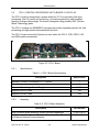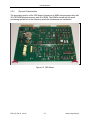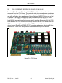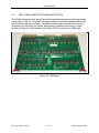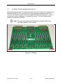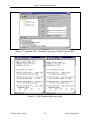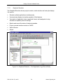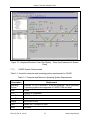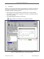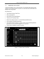
1
VPI II Vital Processor Interlocking Control System Product Overview Copyright © 2006, 2013, 2014, 2015 Alstom Signaling Inc. Read and understand this manual before using this equipment. Failure to follow the instructions presented in this manual can degrade the safety performance of the train control system resulting in property damage, injury, and/or death due to train collision or derailment. Product Overview Manual P2511G VPI II Vital Processor Interlocking Control System Product Overview Copyright © 2006, 2013, 2014, 2015 Alstom Signaling Inc. Read and understand this manual before using this equipment. Failure to follow the instructions presented in this manual can degrade the safety performance of the train control system resulting in property damage, injury, and/or death due to train collision or derailment. Product Overview Manual Alstom Signaling Inc. P2511G, Rev. D, January 2015, Printed in U.S.A. LIST OF EFFECTIVE PAGES P2511G, VPI ® II Vital Processor Interlocking Control System II Product Overview Manual ORIGINAL ISSUE DATE: January 2006 CURRENT REVISION AND DATE: Rev D, January 2015 PAGE CHANGE OR REVISION LEVEL Cover Jan/15 Title page Jan/15 Preface Jan/15 i through x Jan/15 1–1 through 1–18 Jan/15 2–1 through 2–8 Jan/15 3–1 through 3–4 Jan/15 4–1 through 4–10 Jan/15 5–1 through 5–54 Jan/15 6–1 through 6–20 Jan/15 7–1 through 7–14 Jan/15 8–1 through 8–8 Jan/15 P2511G, Rev. D, Jan/15 Alstom Signaling Inc. P2511G, Rev. D, Jan/15 Alstom Signaling Inc. PREFACE NOTICE OF CONFIDENTIAL INFORMATION Information contained herein is confidential and is the property of Alstom Signaling Inc. Where furnished with a proposal, the recipient shall use it solely to evaluate the proposal. Where furnished to customer, it shall be used solely for the purposes of inspection, installation, or maintenance. Where furnished to a supplier, it shall be used solely in the performance of the contract. The information shall not be used or disclosed by the recipient for any other purposes whatsoever. VPI® is a registered trademark of Alstom Signaling Inc. iVPI™ is a trademark of Alstom Signaling Inc. All other trademarks referenced herein are trademarks of their respective owners. FOR QUESTIONS AND INQUIRIES, CONTACT CUSTOMER SERVICE Address: Alstom Signaling Inc. 1025 John Street West Henrietta, NY 14586 USA Website: www.alstomsignalingsolutions.com Email: [email protected] Phone: 1–800–717–4477 P2511G, Rev. D, Jan/15 Alstom Signaling Inc. REVISION LOG Revision Date By Checker Approver 0(A) Jan. 2006 Original issue MAS KWW NI B November 2013 Updated with new commercialized equipment SG KW MS C August 2014 Updated warnings SG KW MS D January 2015 Updated for clarity; added additional warnings; added Safety Warnings section SG KW MS P2511G, Rev. D, Jan/15 Description Alstom Signaling Inc. ABOUT THE MANUAL This manual introduces the Alstom Vital Processor Interlocking Control System (VPI II). The information in this manual is arranged into sections. The title and a brief description of each section follow: Section 1 – SAFETY WARNINGS: This section contains the safety information presented as warnings applicable to the VPI II system. Section 2 – GENERAL DESCRIPTION: This section describes the manual organization, introduces the topics enclosed, and provides a glossary of terms used in this manual. Section 3 – VPI II ORGANIZATION: This section gives general information on function and organization of the VPI II System. Section 4 – CHASSIS CONFIGURATION: This section describes the chassis used for the VPI II System. Section 5 – VITAL SUBSYSTEM: This section describes the Vital boards and assemblies used in the VPI II System. Section 6 – NON-VITAL SUBSYSTEM: This section describes the non-vital boards and assemblies used in the VPI II System. Section 7 – DESIGN, TEST AND VALIDATION TOOLS: This section describes the design, test and validation tools used for the VPI II System. Section 8 – NON-VITAL SYSTEM AND COMMUNICATIONS SOFTWARE: This section describes the non-vital system and communications software used in the VPI II System. P2511G, Rev. D, Jan/15 Alstom Signaling Inc. P2511G, Rev. D, Jan/15 Alstom Signaling Inc. MANUAL SPECIAL NOTATIONS In the Alstom manuals, three methods are used to convey special informational notations. These notations are warnings, cautions, and notes. Both warnings and cautions are readily noticeable by boldface type and a box around the entire informational statement. Warning A warning is the most important notation to heed. A warning is used to tell the reader that special attention needs to be paid to the message because if the instructions or advice is not followed when working on the equipment then the result could be either serious harm or death. The sudden, unexpected operation of a switch machine, for example, or the technician contacting the third rail could lead to injury and/or death. An example of a typical warning notice follows: DISCONNECT MOTOR ENERGY Disconnect the motor energy whenever the gear cover is removed. Otherwise, the switch machine may operate unexpectedly and can cause injury and/or death. Caution A caution statement is used when failure to follow the recommended procedure could result in loss or alteration of data. A typical caution found in a manual is as follows: Changing session date and time to earlier values may affect the ability of the History Window to store data correctly. Note A note is normally used to provide minor additional information to the reader to explain the reason for a given step in a test procedure or to just provide a background detail. An example of the use of a note follows: This step should be done first to validate the correct information is used. P2511G, Rev. D, Jan/15 Alstom Signaling Inc. P2511G, Rev. D, Jan/15 Alstom Signaling Inc. TABLE OF CONTENTS Topic Page SECTION 1 – SAFETY WARNINGS ........................................................................... 1–1 1.1 SAFETY WARNING MATRIX .................................................................... 1–1 1.2 SAFETY WARNINGS ................................................................................ 1–2 SECTION 2 – GENERAL DESCRIPTION ................................................................... 2–1 2.1 SCOPE OF MANUAL ................................................................................ 2–1 2.2 DOCUMENT CONVENTIONS ................................................................... 2–1 2.3 COMMON ABBREVIATIONS AND GLOSSARY ....................................... 2–2 2.4 RELATED PUBLICATIONS ....................................................................... 2–7 SECTION 3 – VPI II ORGANIZATION ........................................................................ 3–1 3.1 GENERAL.................................................................................................. 3–1 3.2 VPI II SUBSYSTEMS................................................................................. 3–1 3.3 GENERAL CHARACTERISTICS ............................................................... 3–2 3.4 GENERAL SPECIFICATIONS ................................................................... 3–3 SECTION 4 – CHASSIS CONFIGURATIONS ............................................................ 4–1 4.1 GENERAL.................................................................................................. 4–1 4.2 PLUG COUPLED CHASSIS ...................................................................... 4–1 4.2.1 Case ................................................................................................ 4–2 4.2.2 Cable Harness ................................................................................ 4–3 4.3 DIRECT WIRE CHASSIS .......................................................................... 4–4 4.3.1 Case ................................................................................................ 4–5 4.3.2 Cables ............................................................................................. 4–6 4.4 PCB INTERFACE CHASSIS ..................................................................... 4–7 4.4.1 Case ................................................................................................ 4–8 4.4.2 Cables ............................................................................................. 4–9 4.4.3 Interface PCBs ................................................................................ 4–9 4.5 COVERS.................................................................................................. 4–10 SECTION 5 – VITAL SUBSYSTEM ............................................................................ 5–1 5.1 GENERAL.................................................................................................. 5–1 5.2 CPU II (CENTRAL PROCESSING UNIT II) BOARD 31166-374-XX ......... 5–2 5.2.1 Specifications .................................................................................. 5–2 5.2.2 Assembly ........................................................................................ 5–2 5.3 VRD (VITAL RELAY DRIVER) BOARD 59473-740-XX ............................. 5–3 5.3.1 VRD Relay ...................................................................................... 5–3 P2511G, Rev. D, Jan/15 i Alstom Signaling Inc. TABLE OF CONTENTS Topic Page 5.3.2 Physical Characteristics .................................................................. 5–7 5.3.3 Specifications .................................................................................. 5–8 5.3.4 Assembly ........................................................................................ 5–8 5.4 VSC (VITAL SERIAL CONTROLLER) BOARD 59473-939-XX ................. 5–9 5.4.1 System Capacity ............................................................................. 5–9 5.4.2 Specifications ................................................................................ 5–10 5.4.3 Assemblies .................................................................................... 5–11 5.5 CRG (CODE RATE GENERATOR) BOARD 31166-261-XX ................... 5–12 5.5.1 Specifications ................................................................................ 5–13 5.5.2 Assemblies .................................................................................... 5–13 5.6 IOB (I/O BUS INTERFACE) BOARD 59473-827-XX ............................... 5–14 5.6.1 Specifications ................................................................................ 5–15 5.6.2 Assembly ...................................................................................... 5–15 5.7 DI (DIRECT INPUT) BOARD 59473-867-XX ........................................... 5–16 5.7.1 Specifications ................................................................................ 5–17 5.7.2 Assemblies .................................................................................... 5–18 5.8 VITAL DC OUTPUT BOARDS 59473-739-XX, -747-XX, -977-XX, 749-XX, 31166-340-XX ............................................................................ 5–19 5.8.1 SBO Board .................................................................................... 5–20 5.8.1.1 Specifications ........................................................................ 5–21 5.8.1.2 Assembly .............................................................................. 5–21 5.8.2 DBO and DBO-50V Board ............................................................ 5–22 5.8.2.1 Specifications ........................................................................ 5–23 5.8.2.2 Assemblies ............................................................................ 5–24 5.8.3 LDO Board .................................................................................... 5–25 5.8.3.1 Specifications ........................................................................ 5–26 5.8.3.2 Assemblies ............................................................................ 5–26 5.8.4 LDO2 Board .................................................................................. 5–27 5.8.4.1 Specifications ........................................................................ 5–29 5.8.4.2 Assemblies ............................................................................ 5–29 5.9 ACO (VITAL AC OUTPUT BOARD) 59473-937-XX ................................ 5–30 5.9.1 Specifications ................................................................................ 5–32 5.9.2 Assembly ...................................................................................... 5–32 5.10 FSVT (FIELD-SETTABLE VITAL TIMER BOARD) 59473-894-XX .......... 5–33 5.10.1 Specifications ................................................................................ 5–34 5.10.2 Assemblies .................................................................................... 5–34 5.11 APPLICATION ASSUMPTIONS AND CONSTRAINTS ........................... 5–35 5.11.1 Application Assumption/Requirements .......................................... 5–35 5.11.1.1 System Cycle ........................................................................ 5–35 P2511G, Rev. D, Jan/15 ii Alstom Signaling Inc. TABLE OF CONTENTS Topic Page 5.11.1.2 5.11.1.3 5.11.1.4 5.11.1.5 5.11.1.6 5.11.1.7 5.11.1.8 Vital Timing ........................................................................... 5–35 System Grounding ................................................................ 5–35 Vital Inputs ............................................................................ 5–35 Response Time to a Safety Critical Failure ........................... 5–36 Signaling Logic Ordering ....................................................... 5–36 Vital Output Verification......................................................... 5–36 Preventing Potential Output Circuit Run-Around Paths (Vital Outputs) ....................................................................... 5–36 5.11.1.9 Safety Checks Outputs ......................................................... 5–36 5.11.1.10 Safety Checks System Processing ....................................... 5–36 5.11.1.11 Application Verification .......................................................... 5–37 5.11.1.12 Output Current Check for Output Ports ................................. 5–38 5.11.1.13 Cycles of Forgiveness ........................................................... 5–38 5.11.1.14 Proof of Logic (Primordial Logic Review) .............................. 5–39 5.11.1.15 Short Cycle Timer Protection ................................................ 5–41 5.11.1.16 Output Protection .................................................................. 5–42 5.11.1.17 VRD Relay and VRD Repeaters ........................................... 5–43 5.11.1.18 Simultaneous Failures........................................................... 5–46 5.11.1.19 FMEA Provides Adequate Failure Coverage ........................ 5–46 5.11.1.20 Security of Installation ........................................................... 5–46 5.11.2 Maintenance Assumption .............................................................. 5–47 5.11.2.1 External Input/Output Integrity .............................................. 5–47 5.11.2.2 Site Version/Revision Configuration Control ......................... 5–47 5.11.3 Production Assumptions ............................................................... 5–52 5.11.3.1 System Manufacturing .......................................................... 5–52 5.11.4 External Interface Assumptions..................................................... 5–52 5.11.4.1 I/O Interface .......................................................................... 5–52 5.11.4.2 Vital Serial Links.................................................................... 5–52 5.11.5 Miscellaneous Assumptions .......................................................... 5–54 5.11.5.1 EMC-EMI .............................................................................. 5–54 SECTION 6 – NON-VITAL SUBSYSTEM ................................................................... 6–1 6.1 GENERAL.................................................................................................. 6–1 6.2 NON-VITAL PROCESSOR FAMILY (NVP) ............................................... 6–2 6.2.1 CSEX4 Board, P/N 31166-417-XX .................................................. 6–2 6.2.1.1 Specifications .......................................................................... 6–3 6.2.1.2 CSEX4 Interface Board (P/N 31166-500-XX) ......................... 6–3 6.2.2 CSEX3 (Extended Code System Emulator 3) Board 31166175-XX ............................................................................................ 6–4 6.2.2.1 Specifications .......................................................................... 6–5 P2511G, Rev. D, Jan/15 iii Alstom Signaling Inc. TABLE OF CONTENTS Topic Page 6.2.2.2 Assemblies .............................................................................. 6–5 6.3 NON-VITAL INPUT BOARDS .................................................................... 6–6 6.3.1 NVI (Non-Vital Input) Board 59473-757-XX .................................... 6–6 6.3.1.1 Isolated Inputs ......................................................................... 6–6 6.3.1.2 Specifications .......................................................................... 6–7 6.3.1.3 Assemblies .............................................................................. 6–7 6.3.2 NVID (Non-Vital Input Differential) Board 31166-106-XX ................ 6–8 6.3.2.1 Specifications .......................................................................... 6–8 6.3.2.2 Assemblies .............................................................................. 6–9 6.3.3 NVIDSW (Non-Vital Input Differential Switch) Board 31166276-XX .......................................................................................... 6–10 6.3.3.1 Specifications ........................................................................ 6–11 6.3.3.2 Assemblies ............................................................................ 6–11 6.4 NON-VITAL OUTPUT BOARDS .............................................................. 6–12 6.4.1 Non-Vital Output Boards 59473-785-XX and 59473-936-XX ........ 6–12 6.4.1.1 Isolated Outputs .................................................................... 6–12 6.4.1.2 Specifications ........................................................................ 6–13 6.4.1.3 Assemblies ............................................................................ 6–13 6.4.2 NVO-SNK (Non-Vital Output Sink) Board 31166-123-XX ............. 6–14 6.4.2.1 Specifications ........................................................................ 6–15 6.4.2.2 Assembly .............................................................................. 6–15 6.4.3 NVR (Non-Vital Relay Output) Board 31166-238-XX .................... 6–16 6.4.3.1 Specifications ........................................................................ 6–17 6.4.3.2 Assemblies ............................................................................ 6–17 6.5 TRAIN TO WAYSIDE COMMUNICATIONS BOARDS ............................ 6–18 6.5.1 NVTWC-FSK (Non-Vital TWC FSK) Board 31166-119-XX ........... 6–18 6.5.1.1 Specifications ........................................................................ 6–19 6.5.1.2 Assemblies ............................................................................ 6–19 SECTION 7 – DESIGN, TEST AND VALIDATION TOOLS ........................................ 7–1 7.1 CAAPE - AN INTEGRATED WINDOWS®-BASED CONFIGURATION TOOL .......................................................................... 7–2 7.1.1 Application Verification .................................................................... 7–4 7.1.2 Graphical Simulator ......................................................................... 7–6 7.1.3 CAAPE System Requirements ........................................................ 7–7 7.2 WATCHER ................................................................................................. 7–8 7.3 EMBEDDED DATALOGGER ..................................................................... 7–9 7.4 TRACKER REMOTE DIAGNOSTIC ANALYZER .................................... 7–10 7.4.1 Fault Detection .............................................................................. 7–10 P2511G, Rev. D, Jan/15 iv Alstom Signaling Inc. TABLE OF CONTENTS Topic Page 7.4.2 Logging ......................................................................................... 7–10 7.4.3 Data Retrieval and Report Creation .............................................. 7–10 7.5 TESTWRITE ............................................................................................ 7–11 7.6 MAINTENANCE MANAGEMENT SYSTEM (MMS) ................................. 7–14 SECTION 8 – NON-VITAL SYSTEM AND COMMUNICATIONS SOFTWARE .......... 8–1 8.1 SYSTEM SOFTWARE INTERFACE MATRIX ........................................... 8–1 8.2 APPLICATION ........................................................................................... 8–2 8.2.1 I/O ................................................................................................... 8–2 8.2.2 Logic ............................................................................................... 8–3 8.2.2.1 Logic Statement Types ........................................................... 8–3 8.2.3 Communications ............................................................................. 8–4 8.3 SYSTEM SOFTWARE INTERFACE MATRIX ........................................... 8–5 8.3.1 CSEX4 Communications Protocol Library ....................................... 8–5 8.3.2 System Kernel ................................................................................. 8–5 8.3.3 CSEX1-3 Communications Protocol Library ................................... 8–6 P2511G, Rev. D, Jan/15 v Alstom Signaling Inc. LIST OF FIGURES Figure No. Title Figure 3-1. Figure 3-2. VPI II Breakdown .................................................................................. 3–1 General VPI II System Block Diagram .................................................. 3–4 Figure 4-1. Figure 4-2. Figure 4-3. Figure 4-4. Figure 4-5. Figure 4-6. VPI II Chassis ....................................................................................... 4–1 Plug Coupled Chassis .......................................................................... 4–1 Plug Coupled Chassis Components ..................................................... 4–2 Direct Wire Chassis .............................................................................. 4–4 PCB Interface Chassis ......................................................................... 4–7 PCB Interface Chassis Components .................................................... 4–7 Figure 5-1. Figure 5-2. Figure 5-3. Figure 5-4. Figure 5-5. Figure 5-6. Figure 5-7. Figure 5-8. Figure 5-9. Figure 5-10. Figure 5-11. Figure 5-12. Figure 5-13. Figure 5-14. Figure 5-15. Figure 5-16. Vital Subsystem .................................................................................... 5–1 CPU II Board ........................................................................................ 5–2 VRD Board ........................................................................................... 5–7 VSC Board............................................................................................ 5–9 CRG Board ......................................................................................... 5–12 IOB Board ........................................................................................... 5–14 DI Board ............................................................................................. 5–16 Vital Output Board .............................................................................. 5–19 SBO Port Interface ............................................................................. 5–20 DBO Port Interface ............................................................................. 5–22 LDO Port Interface.............................................................................. 5–25 LDO2 Port Interface............................................................................ 5–27 LDO2 Board Edge Diagnostic Indicators ............................................ 5–27 ACO Board ......................................................................................... 5–30 ACO Port Interface ............................................................................. 5–30 FSVT Board ........................................................................................ 5–33 Figure 6-1. Figure 6-2. Figure 6-3. Figure 6-4. Figure 6-5. Figure 6-6. Figure 6-7. Figure 6-8. Non-Vital Subsystem ............................................................................ 6–1 CSEX3 Board ....................................................................................... 6–4 NVI Board ............................................................................................. 6–6 NVIDSW Board................................................................................... 6–10 NVO Board ......................................................................................... 6–12 NVO-SNK Board................................................................................. 6–14 NVR Board ......................................................................................... 6–16 NVTWC-FSK Board ............................................................................ 6–18 Figure 7-1. Figure 7-2. Figure 7-3. Figure 7-4. CAAPE Non-Vital Relay Application Logic Display ............................... 7–3 Graphical ADV - Compares Logic Input to Output Files w/CRCs ......... 7–5 ADV Compare Application Utility .......................................................... 7–5 Graphical Simulator – Find Application Logic Errors Easily .................. 7–6 P2511G, Rev. D, Jan/15 Page vi Alstom Signaling Inc. LIST OF FIGURES Figure No. Title Figure 7-5. Figure 7-6. Figure 7-7. Figure 7-8. Figure 7-9. Graphical Simulator Track Plan Display – Place Any Parameter On Screen Easily .................................................................................. 7–7 Watcher Main Screen – View Logic and State...................................... 7–8 Screen View of User Data .................................................................... 7–9 TestWrite User View ........................................................................... 7–12 TestWrite Report ................................................................................ 7–13 Figure 8-1. Logic Programming Sample ................................................................. 8–4 P2511G, Rev. D, Jan/15 Page vii Alstom Signaling Inc. LIST OF TABLES Table No. Title Table 1–1. Warning Titles and Location ................................................................. 1–1 Table 2–1. Table 2-2. Common Abbreviations and Glossary .................................................. 2–2 Related Publications ............................................................................. 2–7 Table 3–1. VPI II Specifications .............................................................................. 3–3 Table 4–1. Table 4–2. Table 4–3. Table 4–4. Table 4–5. Table 4–6. Plug Coupled Chassis Part Numbers ................................................... 4–3 Direct Wire Chassis Part Numbers ....................................................... 4–5 PCB Interface Case Part Numbers ....................................................... 4–8 Ribbon Cable Part Numbers ................................................................. 4–9 Interface PCB Part Numbers ................................................................ 4–9 Interface PCB Cover Part Numbers.................................................... 4–10 Table 5–1. Table 5–2. Table 5–3. Table 5–4. Table 5–5. Table 5–6. Table 5–7. Table 5–8. Table 5–9. Table 5–10. Table 5–11. Table 5–12. Table 5–13. Table 5–14. Table 5–15. Table 5–16. Table 5–17. Table 5–18. Table 5–19. Table 5–20. Table 5–21. Table 5–22. Table 5–23. Table 5–24. CPU II Board Specifications ................................................................. 5–2 CPU II Board Assembly ........................................................................ 5–2 VRD Board Specifications .................................................................... 5–8 VRD Board Assembly ........................................................................... 5–8 VSC Board Specifications................................................................... 5–10 VSC Board Assemblies ...................................................................... 5–11 CRG Board Specifications .................................................................. 5–13 CRG Board Assemblies ...................................................................... 5–13 IOB Board Specifications .................................................................... 5–15 IOB Board Assembly .......................................................................... 5–15 DI Board Specifications ...................................................................... 5–17 DI Board Assemblies .......................................................................... 5–18 SBO Board Specifications .................................................................. 5–21 SBO Board Assembly ......................................................................... 5–21 DBO/DBO-50 Board Specifications .................................................... 5–23 DBO Board Assemblies ...................................................................... 5–24 LDO Board Specifications................................................................... 5–26 LDO Board Assemblies ...................................................................... 5–26 LDO2 Board Specifications................................................................. 5–29 LDO2 Board Assemblies .................................................................... 5–29 ACO Board Specifications .................................................................. 5–32 ACO Board Assembly ......................................................................... 5–32 FSVT Board Specifications ................................................................. 5–34 FSVT Board Assemblies .................................................................... 5–34 Table 6–1. Table 6–2. CSEX4 Board Specifications ................................................................ 6–3 CSEX3 Board Specifications ................................................................ 6–5 P2511G, Rev. D, Jan/15 Page viii Alstom Signaling Inc. LIST OF TABLES Table No. Title Table 6–3. Table 6–4. Table 6–5. Table 6–6. Table 6–7. Table 6–8. Table 6–9. Table 6–10. Table 6–11. Table 6–12. Table 6–13. Table 6–14. Table 6–15. Table 6–16. Table 6–17. Table 6–18. CSEX3 Board Assemblies .................................................................... 6–5 NVI Board Specifications ...................................................................... 6–7 NVI Board Assemblies .......................................................................... 6–7 NVID Board Specifications ................................................................... 6–8 NVID Board Assemblies ....................................................................... 6–9 NVIDSW Board Specifications............................................................ 6–11 NVIDSW Board Assemblies ............................................................... 6–11 NVO Board Specifications .................................................................. 6–13 NVOAC Board Specifications ............................................................. 6–13 Non-Vital Output Board Assemblies ................................................... 6–13 NVO-SNK Board Specifications.......................................................... 6–15 NVO-SNK Board Assembly ................................................................ 6–15 NVR Board Specifications .................................................................. 6–17 NVR Board Assemblies ...................................................................... 6–17 NVTWC-FSK Board Specifications..................................................... 6–19 NVTWC-FSK Board Assemblies ........................................................ 6–19 Table 7–1. Computer and Minimum Operating System Requirements .................. 7–7 Table 8–1. Table 8–2. Table 8–3. CSEX4 Communications Protocol Library ............................................ 8–5 Non-Vital Kernel ................................................................................... 8–5 CSEX1-3 Communications Protocol Library ......................................... 8–6 P2511G, Rev. D, Jan/15 Page ix Alstom Signaling Inc. P2511G, Rev. D, Jan/15 x Alstom Signaling Inc. Safety Warnings SECTION 1 – SAFETY WARNINGS 1.1 SAFETY WARNING MATRIX Warnings are presented in Table 1–1 for convenience in locating an applicable warning. Table 1–1. Warning Titles and Location Warning Heading Found on page: Overview Manual Must Be Read In Entirety 1–2 Notification of Service Disruption 1–2 Use of LRUs Not Manufactured by Alstom 1–3, 5–4, 5–43 Use of LRUs Not Repaired by Alstom 1–4, 5–5, 5–44 Use Only Alstom Vital Relay with VRD Board 1–5, 5–5, 5–45 Load Device Restrictions for Code Rate Generator (CRG) Boards 1–5, 5–13 Load Device Restrictions for Single Break Output (SBO) Boards 1–6, 5–20 Load Device Restrictions for Double Break Output (DBO) Boards 1–6, 5–22 Load Device Restrictions for Light Driver Output (LDO) Boards 1–7, 5–25 Load Device Restrictions for Light Driver Output 2 (LDO2) Boards 1–7, 5–28 Load Device Restrictions for Low Current Vital AC Output (ACO) Boards 1–8, 5–31 Load Device Restrictions for High Current Vital AC Output (ACO) Boards 1–8, 5–31 Intended Safe Functionality of the VPI II System Must Be Verified 1–9, 5–37 VPI II Application Must Be Validation Tested 1–10, 5–37 Verifier Must Be Different Than Designer 1–10, 5–38 ADV Input Data Must be Verified Separately—Prior to ADV Process 1–11, 5–39 VPI II Application Must Be Field Tested 1–11, 5–40 Timer Equation Protection Required 1–12, 5–41 Protect Vital Output Equations With VRDFRNT-DI 1–12, 5–6, 5–42 Software Revision Control Must Be Maintained 1–13, 5–47 Unique Site ID Control Must Be Maintained 1–14, 5–48 Accurate Software Revision ID Control Must Be Maintained 1–15, 5–49 Unique System ID Control Must Be Maintained 1–16, 5–50 Vital Communications Require Unique Link and Block Settings 1–17, 5–53 Non-Vital Subsystem is Not Fail-Safe 1–18, 6–1, 8–1 P2511G, Rev. D, Jan/15 1–1 Alstom Signaling Inc. Safety Warnings 1.2 SAFETY WARNINGS OVERVIEW MANUAL MUST BE READ IN ENTIRETY This VPI II Overview manual (P2511G) should be read in its entirety prior to any operational and/or maintenance actions as it contains important safety messages and pertinent VPI II information. Failure to comply may result in an unsafe condition or accident causing property damage, injury, and/or death. NOTIFICATION OF SERVICE DISRUPTION Disruption of VPI II operation poses a potential threat to rail safety. Before shutting down an interlocking for any reason, the railroad dispatcher in charge of the affected route(s) must be notified. Take all steps necessary to ensure the safe passage of traffic is maintained. Failure to comply can degrade the safety performance of the train control system resulting in property damage, injury, and/or death due to train collision or derailment. P2511G, Rev. D, Jan/15 1–2 Alstom Signaling Inc. Safety Warnings USE OF LRUS NOT MANUFACTURED BY ALSTOM Alstom strongly recommends only using Lowest Replaceable Units (LRUs) manufactured by Alstom in order to maintain the safe operation of the train control system. Use of LRUs not manufactured by Alstom in the Alstom train control system can degrade the safety performance of the system resulting in property damage, injury, and/or death due to train collision or derailment. Alstom strongly recommends that a detailed AREMA-compliant safety analysis be performed before using any LRU that is not an Alstom manufactured direct replacement for this Alstom train control system. This safety analysis should be performed by personnel with mastery in the system safety implications of using LRUs not manufactured by Alstom. Responsibility for the adequacy of the safety analysis rests solely with the transit or railroad authority and Alstom will neither review nor approve any such safety analysis. For train control systems designed by Alstom, the transit or railroad authority shall be solely responsible for any consequences to the safety integrity and performance of the train control system in which LRUs not manufactured by Alstom are used in the train control system originally designed, safety certified, and commissioned by Alstom. Alstom assumes no responsibility or liability for the safe performance of the train control system once LRUs not manufactured by Alstom are used. For train control systems not designed by Alstom, the transit or railroad authority shall be solely responsible for any consequences to the safety integrity and performance of the train control system in which LRUs not manufactured by Alstom are used. Alstom assumes no responsibility or liability for the safe performance of the train control system once LRUs not manufactured by Alstom are used. P2511G, Rev. D, Jan/15 1–3 Alstom Signaling Inc. Safety Warnings USE OF LRUS NOT REPAIRED BY ALSTOM Alstom strongly recommends all LRU repairs be performed by Alstom as Alstom uses special components and has developed special assembly and repair techniques to ensure the continued safety of the train control system. Use of LRUs not repaired by Alstom in the Alstom train control system can degrade the safety performance of the system resulting in property damage, injury, and/or death due to train collision or derailment. Alstom strongly recommends that a detailed AREMA-compliant safety analysis be performed before using any LRU not repaired by Alstom in this Alstom train control system. This safety analysis should be performed by personnel with mastery in the system safety implications when using Alstom LRUs not repaired by Alstom. Responsibility for the adequacy of the safety analysis rests solely with the transit or railroad authority and Alstom will neither review nor approve any such safety analysis. For train control systems designed by Alstom, the transit or railroad authority shall be solely responsible for any consequences to the safety integrity and performance of the train control system in which LRUs not repaired by Alstom are used in the train control system originally designed, safety certified, and commissioned by Alstom. Alstom assumes no responsibility or liability for the safe performance of the train control system once LRUs not repaired by Alstom are used. For train control systems not designed by Alstom, the transit or railroad authority shall be solely responsible for any consequences to the safety integrity and performance of the train control system in which LRUs not repaired by Alstom are used. Alstom assumes no responsibility or liability for the safe performance of the train control system once LRUs not repaired by Alstom are used. P2511G, Rev. D, Jan/15 1–4 Alstom Signaling Inc. Safety Warnings USE ONLY ALSTOM VITAL RELAY WITH VRD BOARD Only Alstom VRD relay (P/N 56001-787-05) is to be used with the Alstom VPI II system VRD board. Alstom products are designed to function within all-Alstom systems. The introduction of non-Alstom products into an Alstom VPI II system could have unintended and unforeseeable safety consequences. Failure to comply can degrade the safety performance of the train control system resulting in property damage, injury, and/or death due to train collision or derailment. LOAD DEVICE RESTRICTIONS FOR CODE RATE GENERATOR (CRG) BOARDS Low current Vital CRG boards may fail with up to 3 milliamperes of output leakage current with the system requesting the output to be in the deenergized state. To prevent a potential unsafe condition, any load device attached to a low current Vital output circuit board must not operate at or below 3 milliamperes and must de-activate above 3 milliamperes. This includes all environmental operating conditions and all operating values of the load device over its service life. Failure to follow this requirement may lead to unexpected operation of the load device resulting in property damage, injury, and/or death due to train collision or derailment. P2511G, Rev. D, Jan/15 1–5 Alstom Signaling Inc. Safety Warnings LOAD DEVICE RESTRICTIONS FOR SINGLE BREAK OUTPUT (SBO) BOARDS Low current Vital SBO boards may fail with up to 3 milliamperes of output leakage current with the system requesting the output to be in the deenergized state. To prevent a potential unsafe condition, any load device attached to a low current Vital output circuit board must not operate at or below 3 milliamperes and must de-activate above 3 milliamperes. This includes all environmental operating conditions and all operating values of the load device over its service life. Failure to follow this requirement may lead to unexpected operation of the load device resulting in property damage, injury, and/or death due to train collision or derailment. LOAD DEVICE RESTRICTIONS FOR DOUBLE BREAK OUTPUT (DBO) BOARDS Low current Vital DBO boards may fail with up to 3 milliamperes of output leakage current with the system requesting the output to be in the deenergized state. To prevent a potential unsafe condition, any load device attached to a low current Vital output circuit board must not operate at or below 3 milliamperes and must de-activate above 3 milliamperes. This includes all environmental operating conditions and all operating values of the load device over its service life. Failure to follow this requirement may lead to unexpected operation of the load device resulting in property damage, injury, and/or death due to train collision or derailment. P2511G, Rev. D, Jan/15 1–6 Alstom Signaling Inc. Safety Warnings LOAD DEVICE RESTRICTIONS FOR LIGHT DRIVER OUTPUT (LDO) BOARDS High current Vital LDO boards may fail with up to 50 milliamperes of output leakage current with the system requesting the output to be in the deenergized state. To prevent a potential unsafe condition, any load device attached to a high current Vital output circuit board must not operate at or below 50 milliamperes and must de-activate above 50 milliamperes. This includes all environmental operating conditions and all operating values of the load device over its service life. Failure to follow this requirement may lead to unexpected operation of the load device resulting in property damage, injury, and/or death due to train collision or derailment. LOAD DEVICE RESTRICTIONS FOR LIGHT DRIVER OUTPUT 2 (LDO2) BOARDS High current Vital LDO2 boards may fail with up to 50 milliamperes of output leakage current with the system requesting the output to be in the deenergized state. To prevent a potential unsafe condition, any load device attached to a high current Vital output circuit board must not operate at or below 50 milliamperes and must de-activate above 50 milliamperes. This includes all environmental operating conditions and all operating values of the load device over its service life. Failure to follow this requirement may lead to unexpected operation of the load device resulting in property damage, injury, and/or death due to train collision or derailment. P2511G, Rev. D, Jan/15 1–7 Alstom Signaling Inc. Safety Warnings LOAD DEVICE RESTRICTIONS FOR LOW CURRENT VITAL AC OUTPUT (ACO) BOARDS Low current Vital AC output boards may fail with up to 3 milliamperes of output leakage current with the system requesting the output to be in the deenergized state. To prevent a potential unsafe condition, any load device attached to a low current Vital output circuit board must not operate at or below 3 milliamperes and must de-activate above 3 milliamperes. This includes all environmental operating conditions and all operating values of the load device over its service life. Failure to follow this requirement may lead to unexpected operation of the load device resulting in property damage, injury, and/or death due to train collision or derailment. LOAD DEVICE RESTRICTIONS FOR HIGH CURRENT VITAL AC OUTPUT (ACO) BOARDS High current Vital AC output boards may fail with up to 50 milliamperes of output leakage current with the system requesting the output to be in the deenergized state. To prevent a potential unsafe condition, any load device attached to a high current Vital output circuit board must not operate at or below 50 milliamperes and must de-activate above 50 milliamperes. This includes all environmental operating conditions and all operating values of the load device over its service life. Failure to follow this requirement may lead to unexpected operation of the load device resulting in property damage, injury, and/or death due to train collision or derailment. P2511G, Rev. D, Jan/15 1–8 Alstom Signaling Inc. Safety Warnings INTENDED SAFE FUNCTIONALITY OF THE VPI II SYSTEM MUST BE VERIFIED The safety of the application logic as written is the responsibility of an experienced signal engineer—CAAPE does not make any determination regarding the inherent safety of the logic equations that were entered. Verifying the accuracy with which CAAPE converted the signaling engineer's application data into PROM data structures is aided by CAAPE, but the signaling engineer must make a final determination using information supplied by CAAPE. CAAPE’s compilers are not themselves Vital programs. An additional independent process is needed to verify that the compile was done correctly. This process is required for all Vital applications. An experienced signal engineer must verify the safety of the VPI II data and its application. It is the signaling engineer's responsibility to verify the correctness of the VPI II input data in that it accurately represents the intended safe functionality of the VPI II system. Furthermore, "verify the correctness" means that the signaling engineer (1) is required to compare the input and output data files to verify the CAA has operated correctly and (2) must test the VPI II application in its intended environment before it can be placed in revenue service. Failure to comply can degrade the safety performance of the train control system resulting in property damage, injury, and/or death due to train collision or derailment. P2511G, Rev. D, Jan/15 1–9 Alstom Signaling Inc. Safety Warnings VPI II APPLICATION MUST BE VALIDATION TESTED Prior to revenue service, validation testing must confirm all VPI II application logic is correct and consistent with application requirements. Failure to comply can degrade the safety performance of the train control system resulting in property damage, injury, and/or death due to train collision or derailment. VERIFIER MUST BE DIFFERENT THAN DESIGNER The application engineer responsible for verification (the Checker or Verifier) using the ADV checklist and creating the report shall be independent from the application engineer responsible for designing (the Designer) the VPI II application. Failure to comply can degrade the safety performance of the train control system resulting in property damage, injury, and/or death due to train collision or derailment. P2511G, Rev. D, Jan/15 1–10 Alstom Signaling Inc. Safety Warnings ADV INPUT DATA MUST BE VERIFIED SEPARATELY—PRIOR TO ADV PROCESS Vital system operation requires that the Boolean equations in the Vital application logic must be written correctly, so that by executing the logic, the VPI II system operates safely in accordance with the rules of the transit or railroad authority. The Application Data Verifier (ADV) output report provides a means to compare and verify equivalence between the input and the output application data. However, the Application Data Verifier neither determines the safety suitability of the Boolean expression list nor determines the validity of certain encoded VPI II application data. The input data to the ADV process must be verified for safety separately, prior to the ADV process, and the safety and suitability of the input data is the responsibility of the signaling engineer. The ADV does, however, issue warnings and error messages as a result of non-vital data checking to alert the signaling engineer to possible discrepancies. Failure to comply can degrade the safety performance of the train control system resulting in property damage, injury, and/or death due to train collision or derailment. VPI II APPLICATION MUST BE FIELD TESTED Field testing of a VPI II application is required before placing the location into revenue service. The customer’s testing plan and safety plan define the testing requirements for the VPI II application. Failure to comply can degrade the safety performance of the train control system resulting in property damage, injury, and/or death due to train collision or derailment. P2511G, Rev. D, Jan/15 1–11 Alstom Signaling Inc. Safety Warnings TIMER EQUATION PROTECTION REQUIRED Vital Boolean and timer equations are evaluated in every one-second application cycle regardless of the state of the VRD, therefore every timer equation must include the VRDFRNT-DI vital input as a constituent in order to prevent the timer from running short and completing an evaluation of the equations prematurely. Failure to comply can degrade the safety performance of the train control system resulting in property damage, injury, and/or death due to train collision or derailment. PROTECT VITAL OUTPUT EQUATIONS WITH VRDFRNT-DI Relying on the status of the VRDFRNT-DI Vital input to, in effect, control Vital output devices without including the VRDFRNT-DI Vital input in the respective output equations does not provide fail-safe operation. The VRDFRNT-DI Vital input must be used as a constituent to the Vital output Boolean equations. Failure to comply can degrade the safety performance of the train control system resulting in property damage, injury, and/or death due to train collision or derailment. Customer Application of VRDFRNT-DI in a non-vital manner is done so at the risk managed by the customer (Alstom Signaling takes no responsibility for that risk). P2511G, Rev. D, Jan/15 1–12 Alstom Signaling Inc. Safety Warnings SOFTWARE REVISION CONTROL MUST BE MAINTAINED Failure to properly version control VPI II system software and VPI II application data can result in unintended consequences including train derailment, train collision, personal injury, and/or death. Alstom strongly recommends that strict revision control of the VPI II application data and system software be maintained so that the expected configuration in the train control system is the actual installed configuration. For train control systems designed by Alstom, the transit or railroad authority shall be solely responsible for any modifications whatsoever to the train control system which deviate from Alstom’s originally delivered design, and any consequences to the system’s safety integrity and performance as a result of such modifications. Alstom assumes no responsibility or liability for any modifications to the train control system or for the safe performance of the train control system once Alstom’s originally delivered design has been modified. For train control systems not designed by Alstom, the transit or railroad authority shall be solely responsible for the design of the train control system, and any consequences to the system’s safety integrity and performance as a result of such designs. Alstom assumes no responsibility or liability for any designs or for the safe performance of the train control system. P2511G, Rev. D, Jan/15 1–13 Alstom Signaling Inc. Safety Warnings UNIQUE SITE ID CONTROL MUST BE MAINTAINED Failure to properly assign, maintain and control unique Site IDs for VPI II systems can result in unintended consequences including train derailment, train collision, personal injury, and/or death. Alstom strongly recommends that strict control of the Site IDs be maintained so that the expected configuration of all VPI IIs in the train control system is the actual installed configuration. For train control systems designed by Alstom, the transit or railroad authority shall be solely responsible for any modifications whatsoever to the train control system which deviate from Alstom’s originally delivered design, and any consequences to the system’s safety integrity and performance as a result of such modifications. Alstom assumes no responsibility or liability for any modifications to the train control system or for the safe performance of the train control system once Alstom’s originally delivered design has been modified. For train control systems not designed by Alstom, the transit or railroad authority shall be solely responsible for the design of the train control system, and any consequences to the system’s safety integrity and performance as a result of such designs. Alstom assumes no responsibility or liability for any designs or for the safe performance of the train control system. P2511G, Rev. D, Jan/15 1–14 Alstom Signaling Inc. Safety Warnings ACCURATE SOFTWARE REVISION ID CONTROL MUST BE MAINTAINED Failure to update and maintain the Software Revision IDs for every software change made to the VPI II application data and/or system software (even a re-compile done with no software changes) jeopardizes proper software revision control and can result in unintended consequences including train derailment, train collision, personal injury, and/or death. Alstom strongly recommends that Software Revision IDs be changed with every software change, even a re-compile of unchanged software. Software Revision IDs shall be maintained so that software and application revision control is maintained and the expected configuration of all VPI IIs in the train control system is the actual installed configuration. For train control systems designed by Alstom, the transit or railroad authority shall be solely responsible for any modifications whatsoever to the train control system which deviate from Alstom’s originally delivered design, and any consequences to the system’s safety integrity and performance as a result of such modifications. Alstom assumes no responsibility or liability for any modifications to the train control system or for the safe performance of the train control system once Alstom’s originally delivered design has been modified. For train control systems not designed by Alstom, the transit or railroad authority shall be solely responsible for the design of the train control system, and any consequences to the system’s safety integrity and performance as a result of such designs. Alstom assumes no responsibility or liability for any designs or for the safe performance of the train control system. P2511G, Rev. D, Jan/15 1–15 Alstom Signaling Inc. Safety Warnings UNIQUE SYSTEM ID CONTROL MUST BE MAINTAINED Failure to properly assign, maintain and control a unique System ID for each VPI II system within the entire train control system can result in unintended consequences including train derailment, train collision, personal injury, and/or death. Alstom strongly recommends that strict control of the System IDs be maintained so that the expected configuration of all VPI IIs within the entire train control system is the actual installed configuration. For train control systems designed by Alstom, the transit or railroad authority shall be solely responsible for any modifications whatsoever to the train control system, which deviate from Alstom’s originally, delivered design, and any consequences to the system’s safety integrity and performance as a result of such modifications. Alstom assumes no responsibility or liability for any modifications to the train control system or for the safe performance of the train control system once Alstom’s originally delivered design has been modified. For train control systems not designed by Alstom, the transit or railroad authority shall be solely responsible for the design of the train control system, and any consequences to the system’s safety integrity and performance as a result of such designs. Alstom assumes no responsibility or liability for any designs or for the safe performance of the train control system. P2511G, Rev. D, Jan/15 1–16 Alstom Signaling Inc. Safety Warnings VITAL COMMUNICATIONS REQUIRE UNIQUE LINK AND BLOCK SETTINGS Failure to properly assign, maintain and control unique Link and Block settings for Vital communications within VPI II systems can result in unintended consequences including train derailment, train collision, personal injury, and/or death. The message link and block values must be assigned such that the combination of these values is unique throughout the network. Alstom strongly recommends that strict control of the Link and Block settings be maintained so that the expected configuration of all VPI IIs in the train control system is the actual installed configuration. For train control systems designed by Alstom, the transit or railroad authority shall be solely responsible for any modifications whatsoever to the train control system which deviate from Alstom’s originally delivered design, and any consequences to the system’s safety integrity and performance as a result of such modifications. Alstom assumes no responsibility or liability for any modifications to the train control system or for the safe performance of the train control system once Alstom’s originally delivered design has been modified. For train control systems not designed by Alstom, the transit or railroad authority shall be solely responsible for the design of the train control system, and any consequences to the system’s safety integrity and performance as a result of such designs. Alstom assumes no responsibility or liability for any designs or for the safe performance of the train control system. P2511G, Rev. D, Jan/15 1–17 Alstom Signaling Inc. Safety Warnings NON-VITAL SUBSYSTEM IS NOT FAIL-SAFE The non-vital subsystem and communications software used in the VPI II system is not designed for fail-safe application and must not be used for safety-critical operations. Failure to comply can degrade the safety performance of the train control system resulting in property damage, injury, and/or death due to train collision or derailment. P2511G, Rev. D, Jan/15 1–18 Alstom Signaling Inc. General Description SECTION 2 – GENERAL DESCRIPTION 2.1 SCOPE OF MANUAL This document contains a general description of the Alstom VPI® II Vital Processor Interlocking Control System. It contains basic, system level information, and hardware descriptions and is intended to be used to estimate the items required to satisfy a specific interlocking’s control requirements. 2.2 DOCUMENT CONVENTIONS This document provides a breakdown of the VPI II product into five main subsections: • Chassis • Vital subsystem • Non-vital subsystem • Application tools • Communication protocols. The five main subsections are then subdivided to provide functional descriptions and electrical specifications for each base item (case, PCB, software, etc.) used to develop a complete VPI II system. The VPI II system does not have a fixed chassis layout. The signal engineer is allowed to configure the system within a set of constraints to best meet the needs of each particular application. The Computer Application Package (CAA) is used to configure the VPI II chassis as well as define the Vital and non-vital application logic required for each system. P2511G, Rev. D, Jan/15 2–1 Alstom Signaling Inc. General Description 2.3 COMMON ABBREVIATIONS AND GLOSSARY Terms and abbreviations used throughout this manual are provided in Table 2–1. Table 2–1. Common Abbreviations and Glossary (Cont.) Term Definition or Explanation AC Alternating Current ACO Vital AC Output board ADV Application Data Verifier AF Audio Frequency AlsDload A tool for programming application and system software on VPI®, iVPI, PGK, PGK2, GK3, and AFTC boards AOCD Absence Of Current Detector AREMA American Railway Engineering and Maintenance-of-Way Association ARES Advanced Railroad Electronic System ATCS Automatic Train Control System CAA Computer-Aided Application CAAPE Computer-Aided Application Programming Environment CENELEC European Committee for Electrotechnical Standardization CIC Cable Integrity Check CMOS Complementary Metal-Oxide-Semiconductor, a major class of integrated circuits; CMOS devices use little power and do not produce as much heat as other forms of logic. COF Cycle of Forgiveness Compiler A program that translates a high-level computer language into machine language. CPU Central Processing Unit – the computer section that handles the actual processing of data into information CRC Cyclical redundancy Checks CRG Code Rate Generator board CSEX Extended Code System Emulator board DBO Double Break Output board DC Direct Current Diagnostic The process of detection and isolation of either a malfunction or mistake. P2511G, Rev. D, Jan/15 2–2 Alstom Signaling Inc. General Description Table 2–1. Common Abbreviations and Glossary (Cont.) Term Definition or Explanation Diagnostic Routine A routine designed specifically to locate a malfunction in the computer. DI Direct Input board DIN Rail A metal rail of a standard type widely used for mounting circuit breakers and industrial control equipment inside equipment racks. DPRAM Dual Port Random Access Memory EIA Electronic Industries Alliance EMC Electromagnetic Compatibility EMI Electromagnetic Interference EPROM A programmable read-only memory device that is erasable using high intensity ultra-violet light. Fail-Safe The concept that if a system fails only a safe result will occur. FET Field-Effect Transistor Firmware Instructions stored on a ROM chip FLASH A form of electrically erasable programmable read only memory used with embedded processors FPGA Field Programmable Gate Array FMEA Failure Mode and Effects Analysis FRA Federal Railroad Administration FSK Frequency-shift Keying FSVT Field Settable Vital Timer board GVSC A specific Vital Serial Controller board (VSC) that provides a means of communicating to and from programmable Genrakode modules. GVSCE A specific Vital Serial Controller board (VSC) that provides a means of communicating to and from programmable Genrakode modules. Hardware The electronic section of the computer that stores and manipulates symbols under the direction of the computer. HHT Hand Held terminal ID Identification I/O Input/Output IOB Input/Output (I/O) Bus Interface board Interface Equipment that enables one kind of hardware to be recognized and processed by another kind of hardware. P2511G, Rev. D, Jan/15 2–3 Alstom Signaling Inc. General Description Table 2–1. Common Abbreviations and Glossary (Cont.) Term Definition or Explanation IP Internet Protocol iVPI Alstom’s integrated Vital Processor Interlocking Control System product Latch A mode of operation for a circuit in which an output's state is maintained. LDO Lamp Drive Output board LRU Lowest Replaceable Unit MAC Maintenance Access connection point in a system. This enables the connection of a VT100 compatible terminal to examine system diagnostics and internal operation of the system. MB Megabyte MMS Maintenance Management System MODBUS A messaging structure used to establish master-slave/client-server communication between intelligent devices. Modem A piece of equipment that connects data terminal equipment to a communication line. MUX Multiplexer MVSC A specific Vital Serial Controller board (VSC) application that provides a means of communicating to and from AF Track Circuit modules. NISAL Numerically Integrated Safety Assurance Logic Non-Vital A component or function that is not critical t safety, its failure is not considered critical to the safe operation of a railroad but may be significant operationally. NVI Non-Vital Input board NVID Non-Vital Input Differential board NVIDSW Non-Vital Input Differential Switch board NVO Non-Vital Output board NVOAC Non-Vital Output AC NVO-SNK Non-Vital Output Sink board NVP Non-Vital Processor board (CSEX2 or CSEX3) NVR Non-Vital Relay Output board NVTWC Non-Vital Train to Wayside Communication NVTWC-FSK Non-Vital Train to Wayside Communication- FSK board P2511G, Rev. D, Jan/15 2–4 Alstom Signaling Inc. General Description Table 2–1. Common Abbreviations and Glossary (Cont.) Term Definition or Explanation OSI Model Open Systems Interconnection Model PC Personal Computer PCB Printed Circuit Board PD Polynomial Divider board POR Power On Reset Program A series of instructions for the computer to follow. PROM Programmable Read-Only Memory – programmable memory devices that store firmware. RAM Random Access Memory – this part of memory temporarily stores information that is constantly being changed in the computer; here, words may be stored (written) or read (retrieved) in any order at random. Reset The act of changing a bit value to zero or an output to an inactive condition. Also refers to the startup or restart of a processor-based system. RFI Radio Frequency Interference ROM Read-Only Memory – this part of memory is built in during the integrated circuit fabrication process; ROM content cannot be altered after the chip is produced. RTU Relay Test Unit SBO Single Break Output board Simulator A special program that represents the behavior of a system. SMT Surface Mount Technology SNK Sink Software Programs that direct the activity of the computer. Subroutine A section of a program that carries out a specific operation. Subsystem Used to summarize the Vital or non-vital functions of a VPI II system, as in Vital subsystem and non-vital subsystem. Subsystem (VPI II) One of multiple subracks populated with boards in a system configuration composed of more than one subrack. System (VPI II) One or more subracks populated with boards. Task A program that is run as an independent unit. TCP Transmission Control Protocol TTL Transistor-Transistor Logic P2511G, Rev. D, Jan/15 2–5 Alstom Signaling Inc. General Description Table 2–1. Common Abbreviations and Glossary (Cont.) Term Definition or Explanation TWC Train-to-Wayside Communications User An experienced signaling engineer VA Volt-ampere VAC Volts Alternating Current Validation CENELEC 3.1.67: the activity applied in order to demonstrate, by test and analysis, that the product meets in all respects its specified requirements. VDC Volts Direct Current Verification CENELEC 3.1.68: the activity of determination, by analysis and test, at each phase of the life-cycle, that the requirements of the phase under the consideration meet the output of the previous phase and that the output of the phase under consideration fulfills its requirements. VAC Volts Alternating Current VDC Volts Direct Current Vital Component or Circuit Any device, circuit or software module used to implement a Vital function; a Vital circuit is so named because its function is critical to the operation of certain signals and track equipment. Vital Function A system, subsystem, equipment or component that provides a function critical to safety; it is implemented using fail-safe design principals, hardware, software and/or relays. VPI / VPI II Alstom’s Vital Processor Interlocking Control System product VRD Vital Relay Driver board VRMS Volts Root Mean Square VSC Vital Serial Controller board that provides a means for exchanging the states of Vital interlocking functions between interlocking systems in a Vital manner. VSL Vital Serial Link VSOE Vital Serial Over Ethernet w/o Without P2511G, Rev. D, Jan/15 2–6 Alstom Signaling Inc. General Description 2.4 RELATED PUBLICATIONS Detailed information for applying and configuring a VPI II system is available in the following Alstom publications listed in Table 2-2. Table 2-2. Related Publications Document No. P2511G Title VPI II Product Overview P2511B, V1 Installation, Operation, and Theory P2511B, V2 Chassis Configuration P2511B, V3 Vital Subsystem P2511B, V4 Non-Vital Subsystem P2511B, V5 Maintenance and Troubleshooting P2346 Series P2509 Code/Communication System Publications (contact Alstom Signaling Inc.’s Customer Service at 1-800-7174477 for a specific protocol) Maintenance Management System for Alstom Vital Processor Interlocking Systems (VPI, VPI II, iVPI) P2512A Computer-Aided Application Programming Environment (CAAPE) Software Package User Manual P2512B AlsDload Software Download User Manual P2512E DataLogger P2512D VPI Computer-Aided Application (CAA) Reference Manual P2528 MMS Client/Server for Alstom Vital Processor Interlocking Systems (VPI II/iVPI). P2511G, Rev. D, Jan/15 2–7 Alstom Signaling Inc. General Description THIS PAGE INTENTIONALLY LEFT BLANK. P2511G, Rev. D, Jan/15 2–8 Alstom Signaling Inc. VPI II Organization SECTION 3 – VPI II ORGANIZATION 3.1 GENERAL This section describes the organization of the VPI II system. 3.2 VPI II SUBSYSTEMS The VPI II system can be subdivided into five main subsections as shown in Figure 3-1. VPI II Chassis Vital Subsystem Non-Vital Subsystem Application Tools Communications Protocols Figure 3-1. VPI II Breakdown P2511G, Rev. D, Jan/15 3–1 Alstom Signaling Inc. VPI II Organization 3.3 GENERAL CHARACTERISTICS The VPI II module is a Vital fail-safe, microprocessor-based control system designed to meet the needs of interlocking control for mainline railroads and mass transit applications. Designed as a modular control system, it contains a set of plug-in Printed Circuit Boards that are applied in varying quantities to meet the needs of a specific project. Although one VPI II system is sufficient for many installations, additional systems in distributed arrangements can be added for sites that are more complex (and/or have specific availability requirements). A single VPI II system may include 1 to 4 chassis depending on I/O and arrangement. Single VPI II systems controlling interlockings with 35 point machines have been proposed. However, the largest single VPI II system installed so far has 20 points machines, and the average number of point machines per system tends to be less due to specific project availability requirements. The VPI II system can be mounted in a small, wayside equipment shelter. No special heating or cooling equipment is required for operation in AREMA-specified environments of Class C or Class D (-40 to +70°C). Built-in secondary transient protection is provided for all I/O lines to prevent disruption of service from EMI or other local interference. If required, additional primary protection devices can be added to the external lines to protect against higher level EMI such as pulses from nearby electrical storms. Typically, no interface devices are required between the VPI II inputs and outputs and the standard interlocking appliances. The interlocking relay logic is reduced to either a closed set of Boolean mathematical expressions or expressed graphically using Relay/Ladder Logic diagrams which represent standard relay contact closures energizing coils. Then, using an Alstom Computer-Aided Application Programming Environment (CAAPE) software package, these Boolean expressions are converted into operating instructions for the VPI II microprocessor. Both Vital and non-vital applications are created with the same user interface. The CAAPE software package is also used to configure the hardware of the VPI II chassis. The tool set includes a graphical simulator that allows the signal engineer to exercise the logic before building the hardware. The simulator provides a mechanism for the signal engineer to demonstrate the operation of the interlocking before the design is complete. As such, it can offer clarifying detail to design reviews. The simulator can also be used in presenting the application design to non-signaling personnel, e.g., operating personnel, to insure that the signal design adequately supports the operational needs. The VPI II system has separate subsystems for Vital and non-vital control. The Vital and non-vital logic and hardware are maintained as separate subsystems to allow modifications in one section to not affect the other. These subsystems may share a chassis or may be configured in separate chassis. Refer to Figure 3-2 for a general block diagram of a portion of a control system with two VPI II systems. P2511G, Rev. D, Jan/15 3–2 Alstom Signaling Inc. VPI II Organization 3.4 GENERAL SPECIFICATIONS Table 3–1 lists nominal specifications for the VPI II module (Chassis and Boards). Table 3–1. VPI II Specifications Characteristic Specification Logic Input Power 5 ±0.25 VDC at 8 amperes maximum per module High Voltage Isolation Rating Meets AREMA Wayside Class C and Class D requirements Operating Temperature -40 to +160ºF (-40 to +70ºC) Meets AREMA Wayside Class C and Class D requirements Humidity 0 to 95% Non-Condensing Meets AREMA Wayside Class C and Class D requirements Typical Weight per Module (with some boards) 15 lbs. (6.80 kg) Dimensions 14H × 19W × 23D 1 inches (35.6H × 48.3W × 58.5D cm) 1 Depth includes cable dress at rear of chassis P2511G, Rev. D, Jan/15 3–3 Alstom Signaling Inc. VPI II Organization Control Center Modem Communication System Location 1 Location 2 Modem Modem VPI II System VPI II System Non-Vital Communications Processor Non-Vital Communications Processor Non-Vital I/O Non-Vital I/O Vital Processor Wayside Signals Vital I/O Switch Controls Vital Contacts from Track Circuits Non-Vital Subsystem Vital Serial Link Vital Processor Vital Subsystem Switch Machines Audio Frequency Track Circuits Local Control Panel DC Coded Track Circuits Automatic Dispatcher Data Logger Code Rate Generator Platform Signs Wheel Counters Figure 3-2. General VPI II System Block Diagram P2511G, Rev. D, Jan/15 3–4 Alstom Signaling Inc. Chassis Configurations SECTION 4 – CHASSIS CONFIGURATIONS 4.1 GENERAL This section describes the chassis configurations of the VPI II system, and is organized as shown in Figure 4-1. Chassis Plug Coupled Direct Wire PCB Interface Covers Figure 4-1. VPI II Chassis 4.2 PLUG COUPLED CHASSIS The VPI II plug coupled chassis includes internal cable harness assemblies. These assemblies connect the VPI II PCB I/O point(s) to a series of AMP type M-series plug couplers, mounted on the rear panel of the chassis. The rear panel also contains a 14-pin type M-series plug coupler for the 5 VDC power connection and provisions for up to four 60-way ribbon cable connectors for connecting to expansion chassis. Figure 4-2. Plug Coupled Chassis P2511G, Rev. D, Jan/15 4–1 Alstom Signaling Inc. Chassis Configurations Plug Coupled Chassis Cable Harness Case Figure 4-3. Plug Coupled Chassis Components 4.2.1 Case The VPI II plug coupled chassis can be provided in two basic case configurations. One to four chassis can be used to complete a single system. The chassis may be a mixture of the two types. The two basic types are the split motherboard and the continuous motherboard that busses the center connector (P2) of the printed circuit boards together. Each chassis contains 21 printed circuit board slots. The split motherboard version of the chassis is configured to connect the P2 connector traces from chassis slots one through five together and slots six through twenty-one together. Since the VPI II system uses the P2 connector as the I/O bus, this allows Vital and non-vital I/O to be housed in the same chassis. For example, the first five chassis slots could be used to house non-vital I/O and the non-vital processor. Slots from 6 to 21 could contain Vital I/O along with the Vital I/O controller (I/O bus). Other system boards may also be required to configure a proper operating system and several other arrangements could be possible. The continuous motherboard version of the plug-coupled module connects all the slots (1–21) of the P2 connector together. This requires that all the I/O housed in the module be either Vital or non-vital. In addition, a CSEX board can be housed in this module with Vital I/O as long as no non-vital I/O is also housed in the module. An extra deep, plug coupled chassis is offered to provide more space for internal cables such as the 38216-497-XX cable assemblies. For those systems with large numbers of I/O’s this makes access to the back of the motherboard and 5 VDC power filter easier. P2511G, Rev. D, Jan/15 4–2 Alstom Signaling Inc. Chassis Configurations Table 4–1. Plug Coupled Chassis Part Numbers Description Part Number Plug coupled chassis with split motherboard (5/16 slots), 5 VDC power filter and 38216-404 Bus Extension Cable 31506-015-01 Plug coupled chassis with continuous motherboard (21 slots), 5 VDC power filter and 38216-404 Bus Extension Cable 31506-015-11 Extra deep plug coupled chassis with rear cover, split motherboard, and 5 VDC power filter 31506-015-15 Extra deep plug coupled chassis with rear cover, continuous motherboard, and 5 VDC power filter 31506-015-16 4.2.2 Cable Harness The chassis requires specific cable harness assemblies to be installed based on the PCB configuration. Ribbon cables are required for the main system bus. This is a 60way ribbon cable, which connects the main system boards together. The number of positions or slots required for this cable is dependent upon the number of main boards being installed. The boards connected by this main bus are CSEX, VRD, CPU II, IOB and VSC. The VRD PCB takes two slots. Cable harnesses are also required to connect the PCB edge connectors to the plug couplers on the rear cover of the chassis. These cables are detailed below. There are 21 available plug coupler locations on the rear panel and four 60 way ribbon cable locations. The blank plates listed below are used to cover the unused locations. Also, there are several variations of output and input cables to provide a variety of arrangements of plug couplers and board configurations. P2511G, Rev. D, Jan/15 4–3 Alstom Signaling Inc. Chassis Configurations 4.3 DIRECT WIRE CHASSIS The direct wire chassis is configured to allow the I/O wiring to be economical by directly inserting wire into the PCB edge connectors in the chassis. This chassis configuration does not allow for quick removal of the chassis from a wired rack. However, all the PCBs can be removed and no active electronic components are left in the chassis. This version is intended for applications where the rack housing this chassis provides a plugcoupled connection to the other interlocking equipment. Figure 4-4. Direct Wire Chassis P2511G, Rev. D, Jan/15 4–4 Alstom Signaling Inc. Chassis Configurations 4.3.1 Case The VPI II direct wired chassis can be constructed from two basic case configurations. One to four chassis can be used to complete a system. The chassis may be a mixture of the two types. The two basic types are the split motherboard and the continuous motherboard that busses the center connector (P2) of the printed circuit boards together. All chassis contain 21 printed circuit board slots. The split motherboard version of the chassis is configured to connect the P2 connector traces from chassis slots one through five together and slots six through 21 together. Since the VPI II system uses the P2 connector as the I/O bus, this allows Vital and nonvital I/O to be housed in the same chassis. For example, the first five chassis slots could be used to house non-vital I/O and the non-vital processor. Slots from 6 to 21 could contain Vital I/O along with the Vital I/O controller (I/O bus). Other system boards may also be required to configure a proper operating system and several other arrangements could be possible. This chassis can also be supplied with an optional rear panel. This panel is used to provide connection points for diagnostic equipment connections; chassis to chassis ribbon cable connections and power supply connections. Table 4–2. Direct Wire Chassis Part Numbers Description Part Number Direct wired chassis with rear panel, split motherboard, and 5 VDC power filter, for use with 38216-404-KN bus ext. cables 31506-015-02 Chassis with split motherboard, 5 VDC power filter, NO rear panel or rear cover 31506-015-03 Direct wired chassis with rear panel, continuous motherboard, and 5 VDC power filter 31506-015-12 Chassis with continuous motherboard, 5 VDC power filter, NO rear panel or rear cover 31506-015-13 Direct wired chassis with rear panel, split motherboard, and 5 VDC power filter, for use with 38216-504-KN bus ext. cables 31506-015-14 Direct wired chassis with split motherboard, rear cover 31506-015-17 Direct wired, deep chassis with continuous motherboard, rear cover 31506-015-18 P2511G, Rev. D, Jan/15 4–5 Alstom Signaling Inc. Chassis Configurations 4.3.2 Cables The chassis required specific cables to be installed based on the PCB configuration. Cables are required for the main system bus. This is a 60-way ribbon cable, which connects the main system boards together. The number of positions or slots required for this cable is dependent upon the number of main boards being installed. The boards connected by this main bus are CSEX, VRD, CPU II, IOB and VSC. The VRD board takes two slots. P2511G, Rev. D, Jan/15 4–6 Alstom Signaling Inc. Chassis Configurations 4.4 PCB INTERFACE CHASSIS The PCB interface chassis uses printed circuit cards with WAGO style (spring clip) wire termination blocks and PCB edge connectors to map the I/O termination points on the VPI II PCBs to discrete wire connectors. The chassis is designed to allow these interface PCBs to be inserted and removed from the rear of the chassis. This provides a wire termination method that can be quickly disconnected (by removing the PCBs) and individual I/O points may be disconnected for troubleshooting. This chassis style is intended for low density applications. See Figure 4-5 for a photo of a PCB Interface Chassis. Figure 4-5. PCB Interface Chassis PCB Interface Chassis Case Interface Boards Figure 4-6. PCB Interface Chassis Components P2511G, Rev. D, Jan/15 4–7 Alstom Signaling Inc. Chassis Configurations 4.4.1 Case The PCB Interface case is similar in arrangement and options to the plug-coupled and direct wired cases. The difference in this case is that an additional set of card guides is installed on the rear of the chassis for the interface PCBs. The case descriptions in Table 4–3 include a list of the boards in each case. The individual boards are discussed under SECTION 5 – Vital Subsystem and SECTION 6 – Non-Vital Subsystem. This chassis uses a fixed PCB for the main system bus and therefore a main system cable is not used. Table 4–3. PCB Interface Case Part Numbers Description Part Number Case with split MB, VRD, IOB, CPU II, DI and DBO 31038-274-01 Case with split MB, CSEX3, VRD, IOB, CPU II, VSC, DI, DBO and LDO 31038-274-02 Case with split MB, CSEX3, VRD, IOB, CPU II, VSC, FSVT, DI, DBO and LDO 31038-274-03 Case with split MB, CSEX3, VRD, IOB, CPU II, VSC, DI, DBO and LDO 31038-274-04 Case with split MB, CSEX3, VRD, IOB, CPU II, VSC, DI and DBO 31038-274-05 P2511G, Rev. D, Jan/15 4–8 Alstom Signaling Inc. Chassis Configurations 4.4.2 Cables The following 60-conductor ribbon cables support connection of CPU/PD or CPU II header and rear panel bulkhead mount to support connection to CPU II/CPU/PD assembly via 38216-589-00 cable. The following 10-conductor ribbon cables support the connection of CRG Boards to the CPU/PD or CPU II Boards. Table 4–4. Ribbon Cable Part Numbers Board Connect Between Description Part Number CPU/PD or CPU II Board Header Rear Panel VPI case 60 Conductor Ribbon Cable, 18 inches 38216-625-01 CPU/PD or CPU II Board Header Rear Panel VPI case 60 Conductor Ribbon Cable, 27 inches 38216-625-02 CRG Board 31166544-01 (P1 Interconnect) CRG Board 31166544-01 (P1 Interconnect) 10 Conductor Ribbon Cable, 6 inches 38216-629-00 CPU/PD or CPU II Board 31166-543-01 (P3 Interconnect) CRG Board 31166544-01 (P1 Interconnect) 10 Conductor Ribbon Cable, 18 inches 38216-630-00 4.4.3 Interface PCBs Table 4–5. Interface PCB Part Numbers Description Part Number Vital output PCB interface 31166-194-01 Vital input interface 31166-195-01 Non-Vital interface 31166-196-01 VRD and 5 VDC Power interface 31166-197-01 VSC interface 31166-198-01 Communications interface (CSEX) 31166-199-01 CPU II interface 31166-336-01 P2511G, Rev. D, Jan/15 4–9 Alstom Signaling Inc. Chassis Configurations 4.5 COVERS The VPI II chassis can be supplied with optional covers. The front cover is a hinged aluminum cover on which the PCB label is generally mounted. The chassis can also be supplied with either a top or bottom screen or both. This screen is generally used to prevent items from falling into the PCB area of the equipment. Table 4–6. Interface PCB Cover Part Numbers Description Part Number Front cover 58605-043-02 Top/bottom screen cover 50253-354-00 P2511G, Rev. D, Jan/15 4–10 Alstom Signaling Inc. Vital Subsystem SECTION 5 – VITAL SUBSYSTEM 5.1 GENERAL This section describes the Vital subsystem of the VPI II system, and is organized as shown in Figure 5-1. Vital Subsystem CPU II VSC VRD IOB CRG Vital Outputs Vital Inputs Figure 5-1. Vital Subsystem P2511G, Rev. D, Jan/15 5–1 Alstom Signaling Inc. Vital Subsystem 5.2 CPU II (CENTRAL PROCESSING UNIT II) BOARD 31166-374-XX The CPU II board is designed as a system board for VPI II incorporating Vital logic processing, Vital I/O control and monitoring, on-board programming, and extended capacity for larger interlockings. The board is designed using primarily SMT (Surface Mount Technology) parts. The CPU II contains two 80386EX33 microprocessors that separately perform the Vital processing and high-speed communications functions. The CPU II board controls the System bus over which the CPU II, VRD, CSEX, VSC and IOB boards communicate. Figure 5-2. CPU II Board 5.2.1 Specifications Table 5–1. CPU II Board Specifications Description Specification Maximum number of Boards per VPI II System 1 Board slots required 1 Maximum Board Logic Current Supply 1.5A Supports 29F010 Flash Yes Supports 29F040 Flash Yes 5.2.2 Assembly Table 5–2. CPU II Board Assembly Description Part Number Vital Processor board assembly without Ethernet capabilities 31166-374-01 Vital Processor board assembly with a Communications Processor for Ethernet Network Communications 31166-374-02 P2511G, Rev. D, Jan/15 5–2 Alstom Signaling Inc. Vital Subsystem 5.3 VRD (VITAL RELAY DRIVER) BOARD 59473-740-XX This board plays a key role in assuring the vitality of the system. It produces an output voltage that operates a 100-ohm Alstom Type B1 relay (P/N 56001-787-05) if, and only if, the data sent to it by the main processing system is exactly correct. If any of these checkwords are not precisely correct, the VRD output is shut off and the external relay de-energizes. The field energy that is delivered to the Vital output boards is broken through front contacts of this Vital relay or a repeater of it. Thus, power will be removed from the outputs when the Vital checkwords are incorrect. 5.3.1 VRD Relay USE ONLY ALSTOM VITAL RELAY WITH VRD BOARD Only Alstom VRD relay (P/N 56001-787-05) is to be used with the Alstom VPI II system VRD board. Alstom products are designed to function within all-Alstom systems. The introduction of non-Alstom products into an Alstom VPI II system could have unintended and unforeseeable safety consequences. Failure to comply can degrade the safety performance of the train control system resulting in property damage, injury, and/or death due to train collision or derailment. P2511G, Rev. D, Jan/15 5–3 Alstom Signaling Inc. Vital Subsystem USE OF LRUS NOT MANUFACTURED BY ALSTOM Alstom strongly recommends only using Lowest Replaceable Units (LRUs) manufactured by Alstom in order to maintain the safe operation of the train control system. Use of LRUs not manufactured by Alstom in the Alstom train control system can degrade the safety performance of the system resulting in property damage, injury, and/or death due to train collision or derailment. Alstom strongly recommends that a detailed AREMA-compliant safety analysis be performed before using any LRU that is not an Alstom manufactured direct replacement for this Alstom train control system. This safety analysis should be performed by personnel with mastery in the system safety implications of using LRUs not manufactured by Alstom. Responsibility for the adequacy of the safety analysis rests solely with the transit or railroad authority and Alstom will neither review nor approve any such safety analysis. For train control systems designed by Alstom, the transit or railroad authority shall be solely responsible for any consequences to the safety integrity and performance of the train control system in which LRUs not manufactured by Alstom are used in the train control system originally designed, safety certified, and commissioned by Alstom. Alstom assumes no responsibility or liability for the safe performance of the train control system once LRUs not manufactured by Alstom are used. For train control systems not designed by Alstom, the transit or railroad authority shall be solely responsible for any consequences to the safety integrity and performance of the train control system in which LRUs not manufactured by Alstom are used. Alstom assumes no responsibility or liability for the safe performance of the train control system once LRUs not manufactured by Alstom are used. P2511G, Rev. D, Jan/15 5–4 Alstom Signaling Inc. Vital Subsystem USE OF LRUS NOT REPAIRED BY ALSTOM Alstom strongly recommends all LRU repairs be performed by Alstom as Alstom uses special components and has developed special assembly and repair techniques to ensure the continued safety of the train control system. Use of LRUs not repaired by Alstom in the Alstom train control system can degrade the safety performance of the system resulting in property damage, injury, and/or death due to train collision or derailment. Alstom strongly recommends that a detailed AREMA-compliant safety analysis be performed before using any LRU not repaired by Alstom in this Alstom train control system. This safety analysis should be performed by personnel with mastery in the system safety implications when using Alstom LRUs not repaired by Alstom. Responsibility for the adequacy of the safety analysis rests solely with the transit or railroad authority and Alstom will neither review nor approve any such safety analysis. For train control systems designed by Alstom, the transit or railroad authority shall be solely responsible for any consequences to the safety integrity and performance of the train control system in which LRUs not repaired by Alstom are used in the train control system originally designed, safety certified, and commissioned by Alstom. Alstom assumes no responsibility or liability for the safe performance of the train control system once LRUs not repaired by Alstom are used. For train control systems not designed by Alstom, the transit or railroad authority shall be solely responsible for any consequences to the safety integrity and performance of the train control system in which LRUs not repaired by Alstom are used. Alstom assumes no responsibility or liability for the safe performance of the train control system once LRUs not repaired by Alstom are used. P2511G, Rev. D, Jan/15 5–5 Alstom Signaling Inc. Vital Subsystem PROTECT VITAL OUTPUT EQUATIONS WITH VRDFRNT-DI Relying on the status of the VRDFRNT-DI Vital input to, in effect, control Vital output devices without including the VRDFRNT-DI Vital input in the respective output equations does not provide fail-safe operation. The VRDFRNT-DI Vital input must be used as a constituent to the Vital output Boolean equations. Failure to comply can degrade the safety performance of the train control system resulting in property damage, injury, and/or death due to train collision or derailment. Customer Application of VRDFRNT-DI in a non-vital manner is done so at the risk managed by the customer (Alstom Signaling takes no responsibility for that risk). Every Vital system requires at least one B relay which is operated by the VRD and through whose front contacts all the energy for the Vital outputs is broken. This relay must be, and must only be replaced by, an Alstom VRD Relay, part number 56001-78705, 100 ohm B relay. A front contact from the VRD Relay must be fed back into the VPI II system as a Vital input for use in the application, for example, to prevent Vital timers from starting when the VRD is de-energized. The name of this Vital input may be VRDFRNT-DI. The front contact used as the Vital input is also available to supply energy to Vital outputs. P2511G, Rev. D, Jan/15 5–6 Alstom Signaling Inc. Vital Subsystem 5.3.2 Physical Characteristics The processing portion of the VRD board is based on an 8085 microprocessor chip with 4K of EPROM program memory and 4K of RAM. The RAM is shared with the main processing system and is the means by which the checkwords are transferred. Figure 5-3. VRD Board P2511G, Rev. D, Jan/15 5–7 Alstom Signaling Inc. Vital Subsystem 5.3.3 Specifications Table 5–3. VRD Board Specifications Description Specification Maximum number of Boards per VPI II System 1 Board slots required 2 Maximum Board Logic Current Supply 300 mA VRD Drive Output Isolation >3000 Vrms Minimum VRD Supply Voltage 9 VDC Maximum VRD Supply Voltage 15 VDC Typical VRD Drive Current draw @ 12.00 V 5.3.4 40 mA Assembly Table 5–4. VRD Board Assembly Description Part Number VRD Board Assembly P2511G, Rev. D, Jan/15 59473-740-02 5–8 Alstom Signaling Inc. Vital Subsystem 5.4 VSC (VITAL SERIAL CONTROLLER) BOARD 59473-939-XX The Vital Serial Controller board is a microprocessor-based board that provides a means for exchanging the states of Vital interlocking functions between interlocking systems in a Vital manner. This board family was first designed to provide Vital VPI II to VPI II Vital communications more efficiently than line wires. There are two types of data transmission interfaces; one for private copper pairs and one for generic, EIA232, DCE connection. A daughter board is used to provide the EIA232 connection, so the number of chassis slots required for this interface is two. Two additional applications of the VSC were created to provide a means of communicating to and from AF Track Circuit modules (MVSC) and programmable Genrakode modules (GVSC or GVSCE). The system software installed on the Vital Serial Controller board is associated with a particular version of system software on the Vital processor board. Each type of board, MVSC, GVSC, GVSCE, or VSC, has its own unique Vital system software that is not interchangeable. 5.4.1 System Capacity Up to ten VSC boards or combinations of VSC, MVSC, GVSC, GVSCE, and CRG boards can be supported by a single Vital subsystem. See Table 5–5 for more information on permissible combinations of these boards. Figure 5-4. VSC Board P2511G, Rev. D, Jan/15 5–9 Alstom Signaling Inc. Vital Subsystem 5.4.2 Specifications Table 5–5. VSC Board Specifications 59473-939- Description Type Maximum number of Boards per VPI II System Board slots required 10 13 14 VSC, MVSC, Pt.-Pt. Multiwith drop full daughter duplex board 4-wire GVSC, Multidrop, half duplex 2-wire 10 (Note 1) 10 (Note 1) 2 (Note 1) 1 2 1 VSC, Pt-Pt 11 12 Maximum Board Logic Current Supply 17 18 GVSCE, Multidrop, half duplex 2-wire VSC, Pt-Pt VSC, Pt.-Pt. with daughter board 2 (Note 2) 2 (Note 2) 10 (Note 1) 10 (Note 1) 1 1 1 2 19200 (Sync.) 9600 or 19200 (Async. or Sync.) 500 mA Baud Rate 19200 (Sync.) 9600 or 19200 (Async. or Sync.) Number of Parameters Supported 200 in each direction 200 in each direction 19200 (Sync.) 19200 (Sync.) 19200 (Sync.) 15 per 25 per 450 in track, up to track, up to 200 in 4 4 each each direction Genrakode Genrakode direction tracks tracks 200 in each direction 1. This limit is 10 minus the sum of (#MVSC + #GVSC + #GVSCE + #CRG + #CSEX), where # indicates the total number of a particular VPI II board type. 2. The total number of GVSCE + GVSC + MVSC combinations must be less than or equal to 2. P2511G, Rev. D, Jan/15 5–10 Alstom Signaling Inc. Vital Subsystem 5.4.3 Assemblies Table 5–6. VSC Board Assemblies Description Part Number VSC Board Assembly, Pt.-Pt. with 40025-322 VSC software (for use with CAA 050B) 59473-939-10 VSC Board Assembly, Pt.-Pt. with daughter board and 40025-322 VSC software (for use with CAA 050B) 59473-939-11 VSC Board Assembly, Multi-drop, full duplex, four-wire with 40025323 MVSC software (for use with CAA 050B and later) 59473-939-12 VSC Board Assembly, Multi-drop, half duplex, two-wire with 40025324 GVSC software for use with CAA 050B and later) 59473-939-13 VSC Board Assembly, Multi-drop, half duplex, two-wire with 40025348 GVSCE software (for use with CAA 050B and later) 59473-939-14 VSC Board Assembly, Pt.-Pt. with 40025-406 VSC Software (for use with CAA 31746-51A, 100D and later) 59473-939-17 VSC Board Assembly, Pt.-Pt. with daughter board and 40025-406 VSC software (for use with CAA 31746-51A, 100D and later) 59473-939-18 P2511G, Rev. D, Jan/15 5–11 Alstom Signaling Inc. Vital Subsystem 5.5 CRG (CODE RATE GENERATOR) BOARD 31166-261-XX The Code Rate Generator Board is a Vital VPI II board that receives code rate commands from the CPU II board. The received code rate commands are decoded and used to generate 8 coded outputs. The frequency and duty-cycle of the coded outputs are vitally verified by using an absence of current detector (AOCD). During the on and off portions of an output’s coding cycle, data is circulated through the AOCD. Data returned from the AOCD, coupled with other Numerically Integrated Safety Assurance Logic (NISAL) processing verifications, are used to generate a message that the CRG board sends to the CPU II board. The message received by the CPU II board from the CRG is used as part of the generation of the VRD checkword. All outputs are generated using a Double Break Output (DBO) DC-DC converter and, as such, are isolated from each other by >2000 Vrms and protected from undetected single fault failures. Figure 5-5. CRG Board P2511G, Rev. D, Jan/15 5–12 Alstom Signaling Inc. Vital Subsystem LOAD DEVICE RESTRICTIONS FOR CODE RATE GENERATOR (CRG) BOARDS Low current Vital CRG boards may fail with up to 3 milliamperes of output leakage current with the system requesting the output to be in the deenergized state. To prevent a potential unsafe condition, any load device attached to a low current Vital output circuit board must not operate at or below 3 milliamperes and must de-activate above 3 milliamperes. This includes all environmental operating conditions and all operating values of the load device over its service life. Failure to follow this requirement may lead to unexpected operation of the load device resulting in property damage, injury, and/or death due to train collision or derailment. 5.5.1 Specifications Table 5–7. CRG Board Specifications Description Specification Maximum number of Boards per VPI II System 3 Board slots required 1 AOCD Current Threshold 3mA Maximum Board Logic Current Supply 5.5.2 1200 mA Assemblies Table 5–8. CRG Board Assemblies Description Part Number CRG Board Assembly for solid state relay code followers; Produces codes of 0, 50, 75, 120, 180 pulses per minute 31166-261-03 CRG Board Assembly for relay code followers; Produces codes of 0, 50, 75, 120, 180, 270, 420 pulses per minute and Steady On 31166-261-04 P2511G, Rev. D, Jan/15 5–13 Alstom Signaling Inc. Vital Subsystem 5.6 IOB (I/O BUS INTERFACE) BOARD 59473-827-XX The I/O Bus Interface board serves as a buffer between the system processing boards and groups of Vital I/O. It provides a storage medium for test data obtained during Vital input and Vital output port checks. The board includes logic to control the continuous verification of Vital output port states. Each chassis containing Vital input or output boards including the Field-Settable Vital Timers (FSVT) must have an IOB board. Figure 5-6. IOB Board P2511G, Rev. D, Jan/15 5–14 Alstom Signaling Inc. Vital Subsystem 5.6.1 Specifications Table 5–9. IOB Board Specifications Description Specification Maximum number of Boards per VPI II System 4 Board slots required 1 Maximum Board Logic Current Supply 300 mA Signature Header 59473-871-01 Board 1 Signature Header 59473-871-02 Board 2 Signature Header 59473-871-03 Board 3 Signature Header 59473-871-04 Board 4 5.6.2 Assembly Table 5–10. IOB Board Assembly Description Part Number IOB Board Assembly 59473-827-01 Signature Header (one for each IOB board in a system) 59473-871-01 through 59473-871-04 P2511G, Rev. D, Jan/15 5–15 Alstom Signaling Inc. Vital Subsystem 5.7 DI (DIRECT INPUT) BOARD 59473-867-XX Direct Input boards contain 16 isolated Vital inputs that each require two connections to the field (+IN and -IN). The inputs are DC current sensing and require a minimum of 12.8 mA. Two inputs may be connected in parallel with opposite polarity (i.e., input a + connected to input b - and input a - connected to input b +) to form a bipolar input (except for board 59473-867-03). The input circuits have been designed to interface with circuits that utilize standard, Vital contacts. Figure 5-7. DI Board P2511G, Rev. D, Jan/15 5–16 Alstom Signaling Inc. Vital Subsystem 5.7.1 Specifications Table 5–11. DI Board Specifications Description 59473-86701 02 03 04 Maximum number of Boards per VPI II System 20 Board slots required 1 Maximum Board Logic Current Supply 05 07 300 mA Minimum Input Voltage/Port 9 VDC 9 VDC 9 VDC 45 VDC 9 VDC 24 VDC Maximum Input Voltage/Port 15 VDC 15 VDC 15 VDC 55 VDC 22 VDC 34 VDC Input Transient Protection Voltage (Max Voltage) 1700 Vrms Input Transient Protection Energy (Max Energy) 3.6 Joules Isolation Between Inputs > 3000 Vrms Address Signature Header Required Yes Equipped with Low-Pass Filter Yes No No Yes Yes Yes Momentary Input Hold No No Yes No No No P2511G, Rev. D, Jan/15 5–17 Alstom Signaling Inc. Vital Subsystem 5.7.2 Assemblies Table 5–12. DI Board Assemblies Description Part Number DI Board Assembly, 16 discrete inputs with filtering (9 - 15 VDC) 59473-867-01 DI Board Assembly, 16 discrete inputs w/o filtering (9 - 15 VDC) 59473-867-02 DI Board Assembly, 16 discrete inputs with hold circuit (9 - 15 VDC) 59473-867-03 2 DI Board Assembly, 16 discrete inputs w/o filtering (45 - 55 VDC) 59473-867-04 DI Board Assembly, 16 discrete inputs w/o filtering (9 - 22 VDC) 59473-867-05 DI Board Assembly, 16 discrete inputs w/o filtering (24 - 34 VDC) 59473-867-07 Signature Header (one for each DI board in a system, determined by CAA) 59473-871-01 through 59473-871-16 2 The 59473-867-03 assembly input circuit possesses the ability to rectify AC signals and is intended for special situations only. Consult Alstom on its use. P2511G, Rev. D, Jan/15 5–18 Alstom Signaling Inc. Vital Subsystem 5.8 VITAL DC OUTPUT BOARDS 59473-739-XX, -747-XX, -977-XX, -749-XX, 31166-340-XX There are four types of Vital DC Output boards: • Single Break: SBO, 59473-739-XX • Double Break: DBO, 59473-747-XX • Double Break 50 V: DBO-50V, 59473-977-XX • Lamp Driver: LDO, 59473-749-XX or LDO2, 31166-340-XX All are configured with eight Vital outputs per board. The single break output is analogous to a single relay contact placed in the positive or feed side of the circuit. The equivalent to the relay contact in the solid state circuit is the FET switch. The double break output is analogous to a relay circuit with the contacts in both the feed and return sides of the circuit. With the solid-state equivalent, however, each output is completely isolated from all other outputs and/or power supplies. The lamp driver's output is equivalent to a single relay contact in the return or common side of the circuit. All outputs use a circuit (AOCD) that detects current to vitally determine the state of the circuit. If the current is greater than the threshold value, the output is considered in the "ON" state. It is only proven to be "OFF" if the current is less than the AOCD threshold. Figure 5-8. Vital Output Board P2511G, Rev. D, Jan/15 5–19 Alstom Signaling Inc. Vital Subsystem 5.8.1 SBO Board The single break output is analogous to a single relay contact placed in the positive or feed side of the circuit. The equivalent of the relay contact in the solid-state circuit is the FET switch. This Vital output board is most often used when driving Vital relays that are part of a special network outside of the VPI II system. Iout Vin SBO LOAD Figure 5-9. SBO Port Interface LOAD DEVICE RESTRICTIONS FOR SINGLE BREAK OUTPUT (SBO) BOARDS Low current Vital SBO boards may fail with up to 3 milliamperes of output leakage current with the system requesting the output to be in the deenergized state. To prevent a potential unsafe condition, any load device attached to a low current Vital output circuit board must not operate at or below 3 milliamperes and must de-activate above 3 milliamperes. This includes all environmental operating conditions and all operating values of the load device over its service life. Failure to follow this requirement may lead to unexpected operation of the load device resulting in property damage, injury, and/or death due to train collision or derailment. P2511G, Rev. D, Jan/15 5–20 Alstom Signaling Inc. Vital Subsystem 5.8.1.1 Specifications Table 5–13. SBO Board Specifications 59473-739- Specification 01 02 Maximum Number of Boards Per VPI II System 40 Board Slots Required 1 Number of Ports per Board 8 Maximum Board Logic Current Supply 500 mA Minimum Switched Output Supply Voltage (Vin) 9.0 VDC Maximum Switched Output Supply Voltage (Vin) 30.0 VDC Typical Output Voltage Drop 1.0 VDC Maximum Switched Power 15 watts AOCD Current Threshold 3 mA Maximum Output Current Per Port (Iout) 500 mA Isolation Between Outputs and 5 Volt Logic > 3000 Vrms Address Signature PROM Required Yes Code Energy Switching No Yes Group Energy Filtered Yes No 5.8.1.2 Assembly Table 5–14. SBO Board Assembly Description Part Number SBO Board Assembly, 8 outputs (9 - 15 VDC) Group energy is filtered 59473-739-01 SBO Board Assembly, 8 outputs (9 - 15 VDC) Group energy is not filtered, supports use of coded energy 59473-739-02 Signature PROM (one for each output board in a system, determined by CAA) 39780-003-01 through 39780-003-40 P2511G, Rev. D, Jan/15 5–21 Alstom Signaling Inc. Vital Subsystem 5.8.2 DBO and DBO-50V Board The double break output is analogous to a relay circuit with the contacts in both the feed and return sides of the circuit. With the solid-state equivalent, however, each output is completely isolated from all other outputs and/or power supplies. Each output is isolated by using individual DC/DC converters that provide in excess of 3000 VRMS isolation. This Vital output board series is used to drive relays, line circuits and most often when a bipolar (pole change) output is required, such as for point machine control. Iout Vin DBO Vout LOAD Figure 5-10. DBO Port Interface LOAD DEVICE RESTRICTIONS FOR DOUBLE BREAK OUTPUT (DBO) BOARDS Low current Vital DBO boards may fail with up to 3 milliamperes of output leakage current with the system requesting the output to be in the deenergized state. To prevent a potential unsafe condition, any load device attached to a low current Vital output circuit board must not operate at or below 3 milliamperes and must de-activate above 3 milliamperes. This includes all environmental operating conditions and all operating values of the load device over its service life. Failure to follow this requirement may lead to unexpected operation of the load device resulting in property damage, injury, and/or death due to train collision or derailment. P2511G, Rev. D, Jan/15 5–22 Alstom Signaling Inc. Vital Subsystem 5.8.2.1 Specifications Table 5–15. DBO/DBO-50 Board Specifications Description 59473-74701 02 59473-97703 Maximum number of Output Boards per VPI II System 40 Board slots required 1 Number of ports per board 8 Maximum Board Logic Current Supply 01 02 500 mA Minimum Input Voltage (Vin) 9 VDC 9 VDC 9 VDC 30 VDC 45 VDC Maximum Input Voltage (Vin) 15 VDC 15 VDC 15 VDC 40 VDC 55 VDC Minimum Output Voltage (Vout) 6 VDC 17.7 VDC 6 VDC 45 VDC 45 VDC Maximum Output Voltage (Vout) 15 VDC 34.5 VDC 15 VDC 55 VDC 55 VDC Maximum Output Current per Port (Iout) 600 mA 300 mA 600 mA 140 mA 140 mA 9W 9W 9W 7.7 W 7.7 W Maximum Output Power per Port AOCD Current Threshold 3 mA Isolation Between Outputs > 3000 Vrms Signature PROM Required Yes P2511G, Rev. D, Jan/15 5–23 Alstom Signaling Inc. Vital Subsystem 5.8.2.2 Assemblies Table 5–16. DBO Board Assemblies Description Part Number DBO Board Assembly, 8 outputs (9 - 15 VDC operation) Not for new designs since board keying is the same as 747-02 assembly DBO Board Assembly, 8 outputs with doubled output voltage (9 - 15 VDC in with 18 - 30 VDC output) 59473-747-01 59473-747-02 DBO Board Assembly, 8 outputs (9 - 15 VDC operation) Preferred for new designs since board keying is different than 747-02 assembly 59473-747-03 DBO Board Assembly, 8 outputs (30 - 40 VDC operation) 59473-977-01 DBO Board Assembly, 8 outputs (45 - 55 VDC operation) 59473-977-02 Signature PROM (one for each output board in a system, determined by CAA) 39780-003-01 through 39780-003-40 P2511G, Rev. D, Jan/15 5–24 Alstom Signaling Inc. Vital Subsystem 5.8.3 LDO Board The lamp drive output circuit handles high current to light signal lamps. Each output circuit can accommodate hot and cold filament checks. This output uses a FET switch in the common or return line of the circuit. Therefore, it is necessary to supply the positive side of the battery or signal lighting supply to the signal lamps. LOAD Iout VIN LDO Figure 5-11. LDO Port Interface LOAD DEVICE RESTRICTIONS FOR LIGHT DRIVER OUTPUT (LDO) BOARDS High current Vital LDO boards may fail with up to 50 milliamperes of output leakage current with the system requesting the output to be in the deenergized state. To prevent a potential unsafe condition, any load device attached to a high current Vital output circuit board must not operate at or below 50 milliamperes and must de-activate above 50 milliamperes. This includes all environmental operating conditions and all operating values of the load device over its service life. Failure to follow this requirement may lead to unexpected operation of the load device resulting in property damage, injury, and/or death due to train collision or derailment. P2511G, Rev. D, Jan/15 5–25 Alstom Signaling Inc. Vital Subsystem 5.8.3.1 Specifications Table 5–17. LDO Board Specifications 59473-749- Description 02 03 Maximum number of Output Boards per VPI II System 40 Board slots required 1 Number of ports per board 8 Maximum Board Logic Current Supply 04 500 mA Minimum Switched Output Supply Voltage (Vin) 9 VDC 15 VDC 9 VDC Maximum Switched Output Supply Voltage (Vin) 18 VDC 30 VDC 18 VDC 2.0 A 2.9 A 2.9 A Maximum Output Current per Port (Iout) Typical Output Voltage Drop 1.7 VDC AOCD Current Threshold 50 mA Isolation Between Outputs and 5 Volt Logic > 3000 Vrms Yes, 100 mA Hot/Cold Filament Check Signature PROM Required 5.8.3.2 Yes, 200 mA Hot 100 mA, no Cold Yes Assemblies Table 5–18. LDO Board Assemblies Description Part Number LDO Board Assembly, 8 outputs (9 - 18 VDC, 2.9 Amp. operation) 59473-749-02 LDO Board Assembly, 8 outputs (15 - 30 VDC, 2.9 Amp. operation) 59473-749-03 LDO Board Assembly, 8 outputs (9 - 18 VDC, 2.9 Amp. operation) 59473-749-04 Signature PROM (one for each output board in a system, determined by CAA) 39780-003-01 through 39780-003-40 P2511G, Rev. D, Jan/15 5–26 Alstom Signaling Inc. Vital Subsystem 5.8.4 LDO2 Board The LDO2 is a Vital VPI II Output board that interfaces with signal lamps. It provides essentially similar functions as the LDO described above. However, this assembly offers the following additional features for each of the eight outputs on each board assembly: • Sourcing Current Drive (positive side switch) • Non-Vital Current Monitor with Over Current Protection and Low Current Detection • Non-Vital Cable Integrity Check (CIC) • Switch Selectable AOCD Signature PROM The board assembly together with improved Vital system software offers enhanced CPU II diagnostic capability. A diagnostic interface on the board edge is provided to permit maintenance personnel to examine the operation of the board without connecting any other equipment. Iout + VIN LDO2 LOAD - Figure 5-12. LDO2 Port Interface Toggle Switch Clear Error Switch Output Number Parameter Data Error LED Reset Switch Requested Output State CFG LED Figure 5-13. LDO2 Board Edge Diagnostic Indicators P2511G, Rev. D, Jan/15 5–27 Alstom Signaling Inc. Vital Subsystem LOAD DEVICE RESTRICTIONS FOR LIGHT DRIVER OUTPUT 2 (LDO2) BOARDS High current Vital LDO2 boards may fail with up to 50 milliamperes of output leakage current with the system requesting the output to be in the deenergized state. To prevent a potential unsafe condition, any load device attached to a high current Vital output circuit board must not operate at or below 50 milliamperes and must de-activate above 50 milliamperes. This includes all environmental operating conditions and all operating values of the load device over its service life. Failure to follow this requirement may lead to unexpected operation of the load device resulting in property damage, injury, and/or death due to train collision or derailment. P2511G, Rev. D, Jan/15 5–28 Alstom Signaling Inc. Vital Subsystem 5.8.4.1 Specifications Table 5–19. LDO2 Board Specifications 31166-340- Description 01 02 Maximum number of Output Boards per VPI II System 40 Board slots required 1 Number of ports per board 8 Maximum Board Logic Current Supply 350mA 250mA Minimum Switched Output Supply Voltage (Vin) 8 VDC Maximum Switched Output Supply Voltage (Vin) 18 VDC Maximum Output Current per Port (Iout) 3.3 A Maximum Output Current per 4-port group 7.5 A Typical Output Voltage Drop on board 1V Cable Integrity Check Detection Voltage 2.0 ±0.3 V Over Current Shutdown Threshold (t = 200 to 400 mS) Low level current detection threshold range 4.0 A none 0.55 to 3.25 in 7 steps none AOCD Current Threshold 50 mA Isolation Between Outputs and 5 Volt Logic > 3000 Vrms Hot/Cold Filament Check Yes, 100 mA Signature PROM Required 5.8.4.2 No Assemblies Table 5–20. LDO2 Board Assemblies Description Part Number LDO2 Board Assembly, 8 outputs (8-18 VDC, 3.3 Amp. operation) 31166-340-01 LDO2 Board Assembly, 8 outputs w/o current monitor (8-18 VDC, 3.3 Amp. operation) 31166-340-02 P2511G, Rev. D, Jan/15 5–29 Alstom Signaling Inc. Vital Subsystem 5.9 ACO (VITAL AC OUTPUT BOARD) 59473-937-XX The Vital AC Output board operates in a manner similar to Vital Output boards. It is used for lighting signal lamps or for operating other AC loads requiring less than 0.8 ampere. Figure 5-14. ACO Board LAMP ` VIN (AC) Iout ACO Figure 5-15. ACO Port Interface P2511G, Rev. D, Jan/15 5–30 Alstom Signaling Inc. Vital Subsystem LOAD DEVICE RESTRICTIONS FOR LOW CURRENT VITAL AC OUTPUT (ACO) BOARDS Low current Vital AC output boards may fail with up to 3 milliamperes of output leakage current with the system requesting the output to be in the deenergized state. To prevent a potential unsafe condition, any load device attached to a low current Vital output circuit board must not operate at or below 3 milliamperes and must de-activate above 3 milliamperes. This includes all environmental operating conditions and all operating values of the load device over its service life. Failure to follow this requirement may lead to unexpected operation of the load device resulting in property damage, injury, and/or death due to train collision or derailment. LOAD DEVICE RESTRICTIONS FOR HIGH CURRENT VITAL AC OUTPUT (ACO) BOARDS High current Vital AC output boards may fail with up to 50 milliamperes of output leakage current with the system requesting the output to be in the deenergized state. To prevent a potential unsafe condition, any load device attached to a high current Vital output circuit board must not operate at or below 50 milliamperes and must de-activate above 50 milliamperes. This includes all environmental operating conditions and all operating values of the load device over its service life. Failure to follow this requirement may lead to unexpected operation of the load device resulting in property damage, injury, and/or death due to train collision or derailment. P2511G, Rev. D, Jan/15 5–31 Alstom Signaling Inc. Vital Subsystem 5.9.1 Specifications Table 5–21. ACO Board Specifications 59473-937- Specification 02 03 Maximum Number of Boards Per VPI System 40 Board Slots Required 1 Number of Ports Per Board 8 Maximum Board Logic Current Supply 500mA Minimum Switched Output Supply Voltage 90 VAC Maximum Switched Output Supply Voltage 130 VAC Frequency Range 40 - 150 Hz AOCD Current Threshold Maximum Output Current Per Port 50 mA 3 mA 0.8 A rms 0.5 A rms Switched Power (max resistive) 104 W Isolation Between Outputs > 3000 Vrms Special EMI Suppression No Address Signature PROM Required 5.9.2 Yes Yes Assembly Table 5–22. ACO Board Assembly Description Part Number ACO Board Assembly, 8 channels with enhanced EMI protection 59473-937-02 ACO Board Assembly, 8 channels with EMI suppression 59473-937-03 Signature PROM (one for each output board in a system, determined by CAA) 39780-003-01 through 39780-003-40 P2511G, Rev. D, Jan/15 5–32 Alstom Signaling Inc. Vital Subsystem 5.10 FSVT (FIELD-SETTABLE VITAL TIMER BOARD) 59473-894-XX The Vital Timer board (59473-894-XX) contains provisions for the use of eight fieldsettable Vital timing functions. Time setting selection is accomplished through the programming of the time selection jumpers. Each of the eight timers has four pin headers that allow setting of the desired time interval by positioning one jumper in each header. The Vital Timer board is located on the Vital I/O bus. Normal operation is to detect the switch setting and then perform a Vital algorithm to verify the setting of that timer's switch. Figure 5-16. FSVT Board P2511G, Rev. D, Jan/15 5–33 Alstom Signaling Inc. Vital Subsystem 5.10.1 Specifications Table 5–23. FSVT Board Specifications 59473-894- Description 01 02 Maximum number of Boards per VPI II System 2 Board slots required 1 Number of Discrete Timers per board 8 Used for Vital Timers Number 1 through 8 9 through 16 Minimum Run Time (minutes/seconds) 0:00 Maximum Run Time (minutes/seconds) 59:59 Assign to I/O Bus With Signature Header Drawing No. (ID letter) 59473-871-01 (A) Jumper TB4 Timer Settings (min/max units seconds) 00/09 seconds Jumper TB3 Timer Settings (min/max tens seconds) 0/50 seconds Jumper TB2 Timer Settings (min/max units minutes) 00/09 minutes Jumper TB1 Timer Settings (min/max tens minutes) 0/50 minutes Time Setting Method 5.10.2 Jumper Selection Assemblies Table 5–24. FSVT Board Assemblies Description Part Number FSVT Board Assembly, 8 timers, for timers one through eight 59473-894-01 FSVT Board Assembly, 8 timers, for timers nine through sixteen 59473-894-02 P2511G, Rev. D, Jan/15 5–34 Alstom Signaling Inc. Vital Subsystem 5.11 APPLICATION ASSUMPTIONS AND CONSTRAINTS Several assumptions have been defined to be used in the application of the generic product and are included here along with any associated product constraints. 5.11.1 5.11.1.1 Application Assumption/Requirements System Cycle VPI II is based on a defined and vitally verified one-second cycle where all inputs, evaluations, and outputs are provided. 5.11.1.2 Vital Timing Application timing is provided based on increments of the vitally ensured VPI II onesecond system cycle. 5.11.1.3 System Grounding VPI II’s internal logic power supply is internally connected to a ground plane, subsequently to the electronics chassis, and, finally, through an external connection to “earth” through proper RFI friendly cables. Typically this is performed by connecting a shielded cable from the equipment rack in which VPI II is mounted to the earth common reference in the equipment room. This grounding is maintained to “shunt” induced RFI away from critical I/O circuits and prevent disruption to system processing. This “earth ground” must be considered when providing connections between VPI II I/O and field devices in order to insure that the earth ground remains isolated from the signaling battery. 5.11.1.4 Vital Inputs Inputs that are considered Vital are expected to be provided by a Vital source such that: • permissive inputs (ON) will be presented as DC signals at the level of the Vital signaling battery (with some tolerance), or • restrictive inputs (OFF) will be presented as no voltage (0 volts) • there is no defined threshold for OFF beyond the assumption that no energy is applied (0 VDC, no connection) or there is no presence of voltage signifying ON at signal battery + voltage level • while VPI II performs input scanning with detection of induced AC (25–250 Hz), proper care must be taken in the installation layout of wiring so that no differentially induced AC signal can be presented to a Vital input where the level of this input could be inappropriately sensed as a permissive state (>3 VDC) P2511G, Rev. D, Jan/15 5–35 Alstom Signaling Inc. Vital Subsystem 5.11.1.5 Response Time to a Safety Critical Failure VPI II has been designed to remove output energy when a failure is detected prior to the period required to have a switch (point) machine begin to move from its intended position (normal or reverse) or to energize a traditional B-Relay (<200 ms). This is considered the worst case safety failure. VPI II’s design maintains a failure detection to energy removal period of 140 ms. Switch machines or other signaling devices that complete state change in less than 200 ms, such as air operated switch machines, must not be directly interfaced to an VPI II system without a Vital relay between the VPI II and the machine to introduce a sufficiently delayed response. 5.11.1.6 Signaling Logic Ordering VPI II evaluates logic in a sequential manner from first expression to last each system cycle. When implementing signaling rules, this fact must be considered to insure proper order of output states and proper sequences of rules implementation. 5.11.1.7 Vital Output Verification VPI II’s detection of failures on outputs is accomplished through the detection of current flow in an output that has been otherwise directed to be in the OFF state. Absence of current in an OFF output is positive proof that no failure has occurred to falsely drive that output. The detection threshold on the absence of current detector is any current over 3 ma for low current output types and 50 ma for high current output types. To provide safe operating margin when designing an interlocking application, it is recommended that VPI II output loads draw more than 5 ma (low current)/100 ma (high current) during normal operation when the output is turned ON. 5.11.1.8 Preventing Potential Output Circuit Run-Around Paths (Vital Outputs) VPI II outputs have been designed for single break (SBO, ACO, LDO) and double break (DBO) application. When designing equipment room and field wiring, care must be taken when using single break outputs so that external failures such as shorted wires cannot introduce a run-around path for output current that could energize an output that should be in the OFF state. 5.11.1.9 Safety Checks Outputs In order to achieve required response time, physical output states (for OFF outputs) and Logic expression results (for ON outputs) are verified every 50 ms. 5.11.1.10 Safety Checks System Processing Verification of system processing checks such as memory integrity, Vital timing, etc., is accomplished once each system’s one-second cycle. P2511G, Rev. D, Jan/15 5–36 Alstom Signaling Inc. Vital Subsystem 5.11.1.11 Application Verification INTENDED SAFE FUNCTIONALITY OF THE VPI II SYSTEM MUST BE VERIFIED The safety of the application logic as written is the responsibility of an experienced signal engineer—CAAPE does not make any determination regarding the inherent safety of the logic equations that were entered. Verifying the accuracy with which CAAPE converted the signaling engineer's application data into PROM data structures is aided by CAAPE, but the signaling engineer must make a final determination using information supplied by CAAPE. CAAPE’s compilers are not themselves Vital programs. An additional independent process is needed to verify that the compile was done correctly. This process is required for all Vital applications. An experienced signal engineer must verify the safety of the VPI II data and its application. It is the signaling engineer's responsibility to verify the correctness of the VPI II input data in that it accurately represents the intended safe functionality of the VPI II system. Furthermore, "verify the correctness" means that the signaling engineer (1) is required to compare the input and output data files to verify the CAA has operated correctly and (2) must test the VPI II application in its intended environment before it can be placed in revenue service. Failure to comply can degrade the safety performance of the train control system resulting in property damage, injury, and/or death due to train collision or derailment. VPI II APPLICATION MUST BE VALIDATION TESTED Prior to revenue service, validation testing must confirm all VPI II application logic is correct and consistent with application requirements. Failure to comply can degrade the safety performance of the train control system resulting in property damage, injury, and/or death due to train collision or derailment. P2511G, Rev. D, Jan/15 5–37 Alstom Signaling Inc. Vital Subsystem VERIFIER MUST BE DIFFERENT THAN DESIGNER The application engineer responsible for verification (the Checker or Verifier) using the ADV checklist and creating the report shall be independent from the application engineer responsible for designing (the Designer) the VPI II application. Failure to comply can degrade the safety performance of the train control system resulting in property damage, injury, and/or death due to train collision or derailment. The basis of the application of VPI II is to use a tool to configure the system hardware and software as well as create the signaling logic for the Vital application. The independent Application Data Verifier Tool, as well as associated procedures, must be run and performed prior to any VPI II application program being tested in field commissioning tests. 5.11.1.12 Output Current Check for Output Ports VPI II has the ability to vitally determine current flow in an output port. This parameter can be used as an internal parameter in the building of the signaling logic rules. This feature is only available for DC-based outputs. AC outputs that are turned ON cannot take advantage of the Vital current check feature, as the check mechanism cannot produce an expected result due to the unsynchronized nature of the output check and the positive voltage peak of the AC cycle. 5.11.1.13 Cycles of Forgiveness Vital inputs, because they are not synchronized to the system cycle, can be sensed to be in an unknown state during transition from ON to OFF, or due to spurious interference to an ON input. This is not a safety-critical issue. A feature termed “cycle of forgiveness” (COF) can be applied to inputs to prevent either of the two input sensing situations from having an undesirable ripple effect on signaling logic. The COF can be used to delay response to a transitional input for a given system cycle. Care must be taken to analyze the overall system response time when COF are assigned to inputs. P2511G, Rev. D, Jan/15 5–38 Alstom Signaling Inc. Vital Subsystem 5.11.1.14 Proof of Logic (Primordial Logic Review) ADV INPUT DATA MUST BE VERIFIED SEPARATELY—PRIOR TO ADV PROCESS Vital system operation requires that the Boolean equations in the Vital application logic must be written correctly, so that by executing the logic, the VPI II system operates safely in accordance with the rules of the transit or railroad authority. The Application Data Verifier (ADV) output report provides a means to compare and verify equivalence between the input and the output application data. However, the Application Data Verifier neither determines the safety suitability of the Boolean expression list nor determines the validity of certain encoded VPI II application data. The input data to the ADV process must be verified for safety separately, prior to the ADV process, and the safety and suitability of the input data is the responsibility of the signaling engineer. The ADV does, however, issue warnings and error messages as a result of non-vital data checking to alert the signaling engineer to possible discrepancies. Failure to comply can degrade the safety performance of the train control system resulting in property damage, injury, and/or death due to train collision or derailment. P2511G, Rev. D, Jan/15 5–39 Alstom Signaling Inc. Vital Subsystem VPI II APPLICATION MUST BE FIELD TESTED Field testing of a VPI II application is required before placing the location into revenue service. The customer’s testing plan and safety plan define the testing requirements for the VPI II application. Failure to comply can degrade the safety performance of the train control system resulting in property damage, injury, and/or death due to train collision or derailment. The application of VPI II depends on application engineers defining configurations and logic to be implemented for the interlocking application. While VPI II guarantees that logic and outputs, etc., are managed vitally, there is no intrinsic check on the correctness or completeness of the signaling logic as it is intended to meet the requirements of the transit/railroad application. It is a primary safety requirement that the logic produced for VPI II execution be independently verified as correct and complete through a “circuit check” type process. The check process must be performed by engineers knowledgeable in the requirements of the signaling rules that govern transit/railroad operation and independent from the engineering staff that produced the logic. P2511G, Rev. D, Jan/15 5–40 Alstom Signaling Inc. Vital Subsystem 5.11.1.15 Short Cycle Timer Protection TIMER EQUATION PROTECTION REQUIRED Vital Boolean and timer equations are evaluated in every one-second application cycle regardless of the state of the VRD, therefore every timer equation must include the VRDFRNT-DI vital input as a constituent in order to prevent the timer from running short and completing an evaluation of the equations prematurely. Failure to comply can degrade the safety performance of the train control system resulting in property damage, injury, and/or death due to train collision or derailment. All VPI II timer equations should include a VRDFRNT-DI parameter to ensure that the timing cannot be “short-timed.” Protection of system timing is provided by check results each one-second timing cycle. Failure of a timer, runs short, would be detected and drop the VRD. However, timing equations continue to evaluate, and therefore a timer equation could prematurely complete. By inserting the VRDFRNT-DI input into a timer equation this situation can be prevented. P2511G, Rev. D, Jan/15 5–41 Alstom Signaling Inc. Vital Subsystem 5.11.1.16 Output Protection PROTECT VITAL OUTPUT EQUATIONS WITH VRDFRNT-DI Relying on the status of the VRDFRNT-DI Vital input to, in effect, control Vital output devices without including the VRDFRNT-DI Vital input in the respective output equations does not provide fail-safe operation. The VRDFRNT-DI Vital input must be used as a constituent to the Vital output Boolean equations. Failure to comply can degrade the safety performance of the train control system resulting in property damage, injury, and/or death due to train collision or derailment. Customer Application of VRDFRNT-DI in a non-vital manner is done so at the risk managed by the customer (Alstom Signaling takes no responsibility for that risk). The primordial logic should be designed to assure that failures in internal and external circuitry, including the VRD Relay and VRD Repeater Relays, result in known safe conditions. All VPI II output control equations should be evaluated by a capable and qualified user (e.g., experienced signal engineer) to include a VRDFRNT-DI parameter to ensure that all outputs, for example signals and vital serial parameters, are placed in a restrictive state in the event of a system failure including a failure in the VRD Relay or VRD Repeater Relay circuitry external from the VPI II system. P2511G, Rev. D, Jan/15 5–42 Alstom Signaling Inc. Vital Subsystem 5.11.1.17 VRD Relay and VRD Repeaters USE OF LRUS NOT MANUFACTURED BY ALSTOM Alstom strongly recommends only using Lowest Replaceable Units (LRUs) manufactured by Alstom in order to maintain the safe operation of the train control system. Use of LRUs not manufactured by Alstom in the Alstom train control system can degrade the safety performance of the system resulting in property damage, injury, and/or death due to train collision or derailment. Alstom strongly recommends that a detailed AREMA-compliant safety analysis be performed before using any LRU that is not an Alstom manufactured direct replacement for this Alstom train control system. This safety analysis should be performed by personnel with mastery in the system safety implications of using LRUs not manufactured by Alstom. Responsibility for the adequacy of the safety analysis rests solely with the transit or railroad authority and Alstom will neither review nor approve any such safety analysis. For train control systems designed by Alstom, the transit or railroad authority shall be solely responsible for any consequences to the safety integrity and performance of the train control system in which LRUs not manufactured by Alstom are used in the train control system originally designed, safety certified, and commissioned by Alstom. Alstom assumes no responsibility or liability for the safe performance of the train control system once LRUs not manufactured by Alstom are used. For train control systems not designed by Alstom, the transit or railroad authority shall be solely responsible for any consequences to the safety integrity and performance of the train control system in which LRUs not manufactured by Alstom are used. Alstom assumes no responsibility or liability for the safe performance of the train control system once LRUs not manufactured by Alstom are used. P2511G, Rev. D, Jan/15 5–43 Alstom Signaling Inc. Vital Subsystem USE OF LRUS NOT REPAIRED BY ALSTOM Alstom strongly recommends all LRU repairs be performed by Alstom as Alstom uses special components and has developed special assembly and repair techniques to ensure the continued safety of the train control system. Use of LRUs not repaired by Alstom in the Alstom train control system can degrade the safety performance of the system resulting in property damage, injury, and/or death due to train collision or derailment. Alstom strongly recommends that a detailed AREMA-compliant safety analysis be performed before using any LRU not repaired by Alstom in this Alstom train control system. This safety analysis should be performed by personnel with mastery in the system safety implications when using Alstom LRUs not repaired by Alstom. Responsibility for the adequacy of the safety analysis rests solely with the transit or railroad authority and Alstom will neither review nor approve any such safety analysis. For train control systems designed by Alstom, the transit or railroad authority shall be solely responsible for any consequences to the safety integrity and performance of the train control system in which LRUs not repaired by Alstom are used in the train control system originally designed, safety certified, and commissioned by Alstom. Alstom assumes no responsibility or liability for the safe performance of the train control system once LRUs not repaired by Alstom are used. For train control systems not designed by Alstom, the transit or railroad authority shall be solely responsible for any consequences to the safety integrity and performance of the train control system in which LRUs not repaired by Alstom are used. Alstom assumes no responsibility or liability for the safe performance of the train control system once LRUs not repaired by Alstom are used. P2511G, Rev. D, Jan/15 5–44 Alstom Signaling Inc. Vital Subsystem USE ONLY ALSTOM VITAL RELAY WITH VRD BOARD Only Alstom VRD relay (P/N 56001-787-05) is to be used with the Alstom VPI II system VRD board. Alstom products are designed to function within all-Alstom systems. The introduction of non-Alstom products into an Alstom VPI II system could have unintended and unforeseeable safety consequences. Failure to comply can degrade the safety performance of the train control system resulting in property damage, injury, and/or death due to train collision or derailment. Every Vital system requires at least one B relay which is operated by the VRD and through whose front contacts all the energy for the Vital outputs is broken. This relay must be, and must only be replaced by, an Alstom VRD Relay, part number 56001-78705, 100 ohm B relay. The VPI II VRD relay is a specific type as it forms the final stage of the Vital circuit residing on the VPI II VRD circuit board. Its pick time and pick-up and drop-away currents are critical parameters in guaranteeing a quick response to a detected failure. The VRD relay is used to disconnect output energy should VPI II encounter a failure in a Vital process, result, or output state. Back contacts of the VRD relay are typically used to drive the Red Aspect of signals to show a positive Stop aspect rather than a dark signal. In large locations, it may be necessary to use a repeater in order to take advantage of the additional contacts for signal lighting. VRD repeaters may also be used to distinguish between feeding output groups from different signaling supply sources. Where either of these situations requiring repeater relays is considered, a response time review should be performed to insure that the added drop times of the repeater relays do not delay the response to a failure detected by VPI II. Depending on repeaters used and arrangement, response time greater than 140 ms will likely be observed. P2511G, Rev. D, Jan/15 5–45 Alstom Signaling Inc. Vital Subsystem 5.11.1.18 Simultaneous Failures Two or more independent self-revealing component failures will not occur simultaneously. This assumption has been traditionally accepted in the train signaling industry. There are three aspects of the assumption, however, which should be emphasized. • The first is the aspect of “independent failures.” Failure modes of individual components may be interrelated in such a way that one failure may precipitate others. These interrelated failures would then constitute one “independent” failure. • The second aspect is that of simultaneity. “Simultaneously” in this context means “during the period bounded by the occurrence of the first independent self-revealing failure and the occurrence of the event which reveals that failure.” • The third aspect is that the maximum component failure rate should be low enough to preclude “simultaneous” failures. 5.11.1.19 FMEA Provides Adequate Failure Coverage The Failure Modes and Effects Criticality Analysis technique, correctly and comprehensively applied, is adequate to reveal all potential unsafe effects of component failure. Justification of this assumption is again based on accepted industry practice (i.e., AREMA). 5.11.1.20 Security of Installation In order to maintain security from physical tampering, VPI II is required to be installed within either an enclosed case (under lock and key) or a locked equipment house where only those trained in the line maintenance or designated members of the rail authority have necessary means of access. P2511G, Rev. D, Jan/15 5–46 Alstom Signaling Inc. Vital Subsystem 5.11.2 5.11.2.1 Maintenance Assumption External Input/Output Integrity VPI II Vitally insures that any safety critical failure that occurs internal to the system (inboard side of the electrical boundaries of its input and output circuit boards) is detected with the system attaining a more restrictive state should a failure occur. VPI II does not have the capability to determine if an erroneously applied energy (positive Vital signal battery voltage) has been applied to its input. In a similar manner, VPI II cannot detect if energy has been erroneously applied to an output drive circuit external to the system thereby supplying a potentially more permissive output state than VPI II has calculated. It is assumed that proper maintenance is being provided by the rail authority to prevent instances of signal circuit shorts which could produce such an occurrence. 5.11.2.2 Site Version/Revision Configuration Control SOFTWARE REVISION CONTROL MUST BE MAINTAINED Failure to properly version control VPI II system software and VPI II application data can result in unintended consequences including train derailment, train collision, personal injury, and/or death. Alstom strongly recommends that strict revision control of the VPI II application data and system software be maintained so that the expected configuration in the train control system is the actual installed configuration. For train control systems designed by Alstom, the transit or railroad authority shall be solely responsible for any modifications whatsoever to the train control system which deviate from Alstom’s originally delivered design, and any consequences to the system’s safety integrity and performance as a result of such modifications. Alstom assumes no responsibility or liability for any modifications to the train control system or for the safe performance of the train control system once Alstom’s originally delivered design has been modified. For train control systems not designed by Alstom, the transit or railroad authority shall be solely responsible for the design of the train control system, and any consequences to the system’s safety integrity and performance as a result of such designs. Alstom assumes no responsibility or liability for any designs or for the safe performance of the train control system. P2511G, Rev. D, Jan/15 5–47 Alstom Signaling Inc. Vital Subsystem UNIQUE SITE ID CONTROL MUST BE MAINTAINED Failure to properly assign, maintain and control unique Site IDs for VPI II systems can result in unintended consequences including train derailment, train collision, personal injury, and/or death. Alstom strongly recommends that strict control of the Site IDs be maintained so that the expected configuration of all VPI IIs in the train control system is the actual installed configuration. For train control systems designed by Alstom, the transit or railroad authority shall be solely responsible for any modifications whatsoever to the train control system which deviate from Alstom’s originally delivered design, and any consequences to the system’s safety integrity and performance as a result of such modifications. Alstom assumes no responsibility or liability for any modifications to the train control system or for the safe performance of the train control system once Alstom’s originally delivered design has been modified. For train control systems not designed by Alstom, the transit or railroad authority shall be solely responsible for the design of the train control system, and any consequences to the system’s safety integrity and performance as a result of such designs. Alstom assumes no responsibility or liability for any designs or for the safe performance of the train control system. P2511G, Rev. D, Jan/15 5–48 Alstom Signaling Inc. Vital Subsystem ACCURATE SOFTWARE REVISION ID CONTROL MUST BE MAINTAINED Failure to update and maintain the Software Revision IDs for every software change made to the VPI II application data and/or system software (even a re-compile done with no software changes) jeopardizes proper software revision control and can result in unintended consequences including train derailment, train collision, personal injury, and/or death. Alstom strongly recommends that Software Revision IDs be changed with every software change, even a re-compile of unchanged software. Software Revision IDs shall be maintained so that software and application revision control is maintained and the expected configuration of all VPI IIs in the train control system is the actual installed configuration. For train control systems designed by Alstom, the transit or railroad authority shall be solely responsible for any modifications whatsoever to the train control system which deviate from Alstom’s originally delivered design, and any consequences to the system’s safety integrity and performance as a result of such modifications. Alstom assumes no responsibility or liability for any modifications to the train control system or for the safe performance of the train control system once Alstom’s originally delivered design has been modified. For train control systems not designed by Alstom, the transit or railroad authority shall be solely responsible for the design of the train control system, and any consequences to the system’s safety integrity and performance as a result of such designs. Alstom assumes no responsibility or liability for any designs or for the safe performance of the train control system. P2511G, Rev. D, Jan/15 5–49 Alstom Signaling Inc. Vital Subsystem UNIQUE SYSTEM ID CONTROL MUST BE MAINTAINED Failure to properly assign, maintain and control a unique System ID for each VPI II system within the entire train control system can result in unintended consequences including train derailment, train collision, personal injury, and/or death. Alstom strongly recommends that strict control of the System IDs be maintained so that the expected configuration of all VPI IIs within the entire train control system is the actual installed configuration. For train control systems designed by Alstom, the transit or railroad authority shall be solely responsible for any modifications whatsoever to the train control system, which deviate from Alstom’s originally, delivered design, and any consequences to the system’s safety integrity and performance as a result of such modifications. Alstom assumes no responsibility or liability for any modifications to the train control system or for the safe performance of the train control system once Alstom’s originally delivered design has been modified. For train control systems not designed by Alstom, the transit or railroad authority shall be solely responsible for the design of the train control system, and any consequences to the system’s safety integrity and performance as a result of such designs. Alstom assumes no responsibility or liability for any designs or for the safe performance of the train control system. P2511G, Rev. D, Jan/15 5–50 Alstom Signaling Inc. Vital Subsystem One hazard condition that needs to be considered with regard to software-based interlocking control is the potential of installing an old and incorrect application or that of a similar application program other than the one required. This could occur through improper maintenance activities. One of the mitigations of this class of failure has been to institute location (site) and revision control features into VPI II. The site and revision ID must be uniquely assigned by the user with each interlocking application change that will be installed in a field location. For CPU/PD or CPU II refer to the application .lvc file for the wire table in order to configure the hardware jumper wires for the compiled revision and site ID values. Alternatively, refer to the application .cfg file for the System ID. The System ID is equivalent to the combination of the Revision ID and Site ID. The System ID board can be configured with the compiled System ID value. VRD will not energize if the Revision ID/Site ID/System ID values configured on the hardware do not match the values configured in the CPU/PD or CPU II application. For CSEX4 refer to the application .cfn file for the Software Revision ID in order to update the High/Low switch settings on the CSEX4 board. The CSEX4 application will not operate if the Revision ID values configured on the CSEX4 hardware do not match the values configured in the CSEX4 application. P2511G, Rev. D, Jan/15 5–51 Alstom Signaling Inc. Vital Subsystem 5.11.3 5.11.3.1 Production Assumptions System Manufacturing VPI II has been designed with the latest state of the art surface mount components and has been fully qualified to international rail industry standards as well as quality standards for complete system component manufacture. It is assumed that the manufacturer of printed circuit boards continues to follow recommended production standards for printed circuit boards and that it is periodically verified though quality inspection that proper production and handling best practices have been performed. It is further assumed that Alstom will be made aware of any change to components, or manufacturing processes of Vital printed circuit boards prior to authorization being given to proceed with the changes. This includes first run production as well as printed circuit boards being cycled through a repair cycle. 5.11.4 5.11.4.1 External Interface Assumptions I/O Interface It needs to be considered that VPI II inputs must not be connected to any external device that can act to rectify an induced AC signal. Inputs that are not static in nature (i.e., ON/OFF), such as dynamic signals, must be reviewed for Vital application. 5.11.4.2 Vital Serial Links VPI II provides two Vital communication protocols called Vital Serial Link (VSL) and Vital Serial Over Ethernet (VSOE). VSL establishes communications over a direct-connect copper interface or through an EIA232 interface with a modem or multiplexer. VSOE is an Ethernet network-based interface. It must be understood that each of the Vital protocols established has taken into account all known hazards associated with the medium of communications, as well as the interconnection of various adjacent VPI, VPI II, iVPI and track circuit systems that reside on the medium. The protocols require that the receiving system must perform the final verification of the message Vital integrity. Connection to other systems requires a thorough review of safety methods used on both sides of the interface to insure that all protections provided for in the VSL and VSOE protocols are maintained. P2511G, Rev. D, Jan/15 5–52 Alstom Signaling Inc. Vital Subsystem 5.11.4.2.1 Vital Serial Link Message Identification VITAL COMMUNICATIONS REQUIRE UNIQUE LINK AND BLOCK SETTINGS Failure to properly assign, maintain and control unique Link and Block settings for Vital communications within VPI II systems can result in unintended consequences including train derailment, train collision, personal injury, and/or death. The message link and block values must be assigned such that the combination of these values is unique throughout the network. Alstom strongly recommends that strict control of the Link and Block settings be maintained so that the expected configuration of all VPI IIs in the train control system is the actual installed configuration. For train control systems designed by Alstom, the transit or railroad authority shall be solely responsible for any modifications whatsoever to the train control system which deviate from Alstom’s originally delivered design, and any consequences to the system’s safety integrity and performance as a result of such modifications. Alstom assumes no responsibility or liability for any modifications to the train control system or for the safe performance of the train control system once Alstom’s originally delivered design has been modified. For train control systems not designed by Alstom, the transit or railroad authority shall be solely responsible for the design of the train control system, and any consequences to the system’s safety integrity and performance as a result of such designs. Alstom assumes no responsibility or liability for any designs or for the safe performance of the train control system. The VSL and VSOE messages must be unique in order to assure safe communications; supported by the assignment of link and block/sub-block numbers. The message link and block/sub-block values must be assigned such that the combination of these values is unique throughout the network. The VSL and VSOE protocols do not protect against spoofing and the user must either maintain a private communications network, or for VSOE, implement a lower-layer (relative to OSI model) network encryption. P2511G, Rev. D, Jan/15 5–53 Alstom Signaling Inc. Vital Subsystem 5.11.5 5.11.5.1 Miscellaneous Assumptions EMC-EMI The nature of the modifications for VPI II in comparison to VPI, are not subject to downgrade original EMC / EMI characteristics. VPI II rack as an incremental evolution of the mature VPI has been tested and qualified to AREMA 11.5.1 Class C Standard. However, this document refers to the executed test on the generic VPI-VPI2-iVPI products, i.e., VPI-VPI2-iVPI rack. EMC-EMI shall be verified in the frame of each Application Project with: • specific control room power supply characteristics, protection and filter where the VPI-VPI2-iVPI rack in installed • specific cubicle project configuration • specific cubicle wiring • specific cubicle and grounding • etc. P2511G, Rev. D, Jan/15 5–54 Alstom Signaling Inc. Non-Vital Subsystem SECTION 6 – NON-VITAL SUBSYSTEM 6.1 GENERAL This section describes the Non-Vital subsystem of the VPI II system, and is organized as shown in Figure 6-1. Non-Vital Subsystem CSEX Non-Vital Inputs Non-Vital Outputs Train to Wayside Communications Figure 6-1. Non-Vital Subsystem NON-VITAL SUBSYSTEM IS NOT FAIL-SAFE The non-vital subsystem and communications software used in the VPI II system is not designed for fail-safe application and must not be used for safety-critical operations. Failure to comply can degrade the safety performance of the train control system resulting in property damage, injury, and/or death due to train collision or derailment. P2511G, Rev. D, Jan/15 6–1 Alstom Signaling Inc. Non-Vital Subsystem 6.2 NON-VITAL PROCESSOR FAMILY (NVP) The non-vital processors perform important communications, data logging and non-vital logic operations within the VPI II system. There have been three generations of processor boards with generally increasing functionality. All the non-vital processors are referred to as CSEX which stands for Code System Emulator eXtended. The first CSEX board family was the 59473-938 series. This board was developed to support multiple, non-vital communications links simultaneously and to permit the separation of the nonvital application from the Vital to better support the non-vital application requirements. The CSEX2 board family, 31166-049 series, enhanced the flexibility of configuration of the non-vital communications interfaces and the first generation of data logging. The latest family, CSEX3, 31166-175 series, was designed to support larger, more demanding non-vital applications and provided a greater depth of memory for data logging. The CSEX3 was also designed to be a plug-in replacement for either the earlier CSEX or CSEX2 board assemblies. 6.2.1 CSEX4 Board, P/N 31166-417-XX The CSEX4 (Code System Emulator eXtended) Board is designed as a system board for VPI II as well as a stand-alone non-vital logic processor. The CSEX4 board provides an interface to non-vital inputs and outputs for local control of an interlocking. The CSEX4 board includes two high integration 386EX microprocessors referred to as the Main Processor and the Communication Processor. • The Main Processor is responsible for managing all non-vital data communication with the CPU 2 board, serial port communication protocol, non-vital bus management and exchanging messages with the Communication Processor through a DPRAM. • The Communication Processor is responsible for managing all Ethernet controller operations and TCP/IP stack operations as well as the interchange of messages to and from the Main Processor. P2511G, Rev. D, Jan/15 6–2 Alstom Signaling Inc. Non-Vital Subsystem 6.2.1.1 Specifications • Operating temperature range: −40°C to +70°C • Storage temperature range: −55°C to +85°C • Humidity: 0% to 95% non-condensing Table 6–1. CSEX4 Board Specifications Specification 31166-417-01 Maximum Number of Boards Per VPI II System 4 Board Slots Required 1 Maximum Board Logic Current Supply Draw 750 mA Power Supply +5V Voltage Range 4.75 V to 5.25 V Typical Operating Current 1.25 A Supports 29040 Flash PROM Yes No. of Sync./Async. Ports 2 No. of Async. Only Ports 3 Ethernet Ports 2 MAC Interface EIA232 Additional Assembly Information 6.2.1.2 DC Code Line CSEX4 Interface Board (P/N 31166-500-XX) The CSEX4 Interface Board is mounted on DIN rails at the rear of the rack. It is connected to the P3 board edge connector on CSEX4 through a ribbon cable at J1. It is used in VPI II configurations for serial communication as well as Ethernet communication. The CSEX4 Interface Board includes 2 serial connections connected using the EIA-530 standard, described in Table 6–1: • J2 carries information from CSEX4 Serial 1 • J3 carries information from CSEX4 Serial 2 MAC from the CSEX4 board is outputted via J4 on the CSEX4 Interface Board using an RJ45 jack without LEDs. The common processor health bit is transmitted from the CSEX4 board to an RJ25 plug (J6) on the CSEX4 Interface Board. P2511G, Rev. D, Jan/15 6–3 Alstom Signaling Inc. Non-Vital Subsystem 6.2.2 CSEX3 (Extended Code System Emulator 3) Board 31166-175-XX The CSEX3 (Code System Emulator eXtended) board is an upgrade for both the CSEX (59473-938-XX) and CSEX2 (31166-049-XX) boards. It is designed as a system board for VPI II as well as a stand-alone non-vital logic processor. The CSEX3 board has six serial ports for communications to external devices, such as modems, other CSEX boards, etc. A DC code line interface is available as well as EIA232, EIA422, and EIA485 interfaces. The CSEX3 board provides an interface to non-vital inputs and outputs for local control of interlockings. Battery-backed RAM is also available for data logging. The CSEX3 board is designed using primarily SMT (Surface Mount Technology) parts. CSEX3 supports up to 20 non-vital I/O boards. Figure 6-2. CSEX3 Board P2511G, Rev. D, Jan/15 6–4 Alstom Signaling Inc. Non-Vital Subsystem 6.2.2.1 Specifications Table 6–2. CSEX3 Board Specifications 31166-175- Description 02 03 Maximum number of Boards per VPI II System 4 Board slots required 1 Maximum Board Logic Current Supply Draw 750 mA Supports 29040 Flash PROM Yes No. of Sync./Async. Ports 2 1 No. of Async. only Ports 3 3 EIA232 EIA232 31166-187-01 31166-187-02 MAC interface Daughterboard used Additional Assembly Information 6.2.2.2 DC Code Line Assemblies Table 6–3. CSEX3 Board Assemblies Description Part Number CSEX3 Board Assembly, 2 EIA232/EIA422/EIA485, 3 EIA422, EIA232/EIA422/EIA485 MAC, blank FLASH PROMs, 36-pin Aux. Bd 31166-175-02 CSEX3 Board Assembly, 1 EIA232/EIA422/EIA485, 1 DC code I/F, 3 EIA422, EIA232/EIA422/EIA485 MAC, blank FLASH PROMs, 36-pin Aux. Bd 31166-175-03 P2511G, Rev. D, Jan/15 6–5 Alstom Signaling Inc. Non-Vital Subsystem 6.3 6.3.1 NON-VITAL INPUT BOARDS NVI (Non-Vital Input) Board 59473-757-XX The Non-Vital Input board provides 32 isolated, non-vital inputs interfaced through the motherboard to the VPI II module. A CSEX board, employing non-vital I/O control software, communicates over the motherboard bus to the NVI board. Input states are latched and read every 25 ms by the NVP board (CSEX2 or CSEX3 board). 6.3.1.1 Isolated Inputs Optical isolators separate the power supplies of the 5V logic system and field circuitry. Each of the four groups of eight inputs has a separate signal return, allowing inputs derived from four isolated supplies to share one input board. Figure 6-3. NVI Board P2511G, Rev. D, Jan/15 6–6 Alstom Signaling Inc. Non-Vital Subsystem 6.3.1.2 Specifications Table 6–4. NVI Board Specifications 59473-757- Description 02 03 Maximum number of Boards per NVP Subsystem 20 Board slots required 1 Number of ports per board 32 Maximum Board Logic Current Supply Draw 200 mA Minimum Input Voltage per Port 18 VDC 9 VDC Maximum Input Voltage per Port 33 VDC 18 VDC Minimum Activation Current per Port 10 mA (Source) 7 mA (Source) 6.3.1.3 Assemblies Table 6–5. NVI Board Assemblies Description Part Number NVI Board Assembly, 32 inputs (18–33 VDC) 59473-757-02 NVI Board Assembly, 32 inputs (9–18 VDC) 59473-757-03 P2511G, Rev. D, Jan/15 6–7 Alstom Signaling Inc. Non-Vital Subsystem 6.3.2 NVID (Non-Vital Input Differential) Board 31166-106-XX The Non-Vital Input Differential board provides 32 isolated non-vital inputs to a VPI II system. Interface to the system is accomplished through the system motherboard. A Code System Emulator employing non-vital I/O control software communicates over the motherboard bus to the NVID board. Every 25 ms input states are latched and then read. On-board jumpers permit configuration of the inputs as common cathode, common anode or isolated (differential). 6.3.2.1 Specifications Table 6–6. NVID Board Specifications Description 31166-10601 02 03 Maximum number of Boards per CSEX Subsystem 20 Board slots required 1 Number of ports per board 32 Maximum Board Logic Current Supply Draw 04 05 200 mA Minimum Input Voltage per Port 4.5 VDC 18 VDC 9 VDC 9 VDC 18 VDC Maximum Input Voltage per Port 14.5 VDC 33 VDC 16 VDC 16 VDC 33 VDC 9 VDC 24 VDC 12 VDC 12 VDC 24 VDC Working Current at Nominal Voltage 5 mA 6 mA 3.6 mA 3.6 mA 6 mA Input Sensitivity (min. input voltage to be read as “1”) ±0.7 VDC ±2 VDC ±0.9 VDC ±3 VDC ±13 VDC Nominal Input Voltage per Port P2511G, Rev. D, Jan/15 6–8 Alstom Signaling Inc. Non-Vital Subsystem 6.3.2.2 Assemblies Table 6–7. NVID Board Assemblies Description Part Number NVID Board Assembly, 32 six volt inputs 31166-106-01 NVID Board Assembly, 32 twenty-four volt inputs 31166-106-02 NVID Board Assembly, 32 twelve volt inputs 31166-106-03 NVID Board Assembly, 32 twelve volt inputs 31166-106-04 NVID Board Assembly, 32 twenty-four volt inputs 31166-106-05 P2511G, Rev. D, Jan/15 6–9 Alstom Signaling Inc. Non-Vital Subsystem 6.3.3 NVIDSW (Non-Vital Input Differential Switch) Board 31166-276-XX The Non-Vital Input Differential Switch Board provides 32 isolated non-vital inputs to a VPI II system. Interface to the system is accomplished through the system motherboard. Input states are latched, and then read, every 25 ms. NVIDSW board assemblies 01 and 03 provide the ability to physically set the state of the inputs through 32 switches located on the front of these boards. Assemblies 02 and 04 function identically to the NVID board, but have no switches. Figure 6-4. NVIDSW Board P2511G, Rev. D, Jan/15 6–10 Alstom Signaling Inc. Non-Vital Subsystem 6.3.3.1 Specifications Table 6–8. NVIDSW Board Specifications 31166-276- Description 01 02 03 Maximum Number of Boards per NVP Subsystem 20 Board Slots Required 1 Number of Ports per Board 32 Maximum Board Logic Current Supply Draw 04 200 mA Minimum Input Voltage per Port 9V 9V 18V 18V Maximum Input Voltage per Port 18V 18V 33V 33V Switches to force each input on/off Yes No Yes No 6.3.3.2 Assemblies Table 6–9. NVIDSW Board Assemblies Description Part Number NVIDSW Board Assembly, 32 inputs with switches to force each input on/off 31166-276-01 NVIDSW Board Assembly, 32 inputs 31166-276-02 NVIDSW Board Assembly, 32 inputs with switches to force each input on/off 31166-276-03 NVIDSW Board Assembly, 32 inputs 31166-276-04 P2511G, Rev. D, Jan/15 6–11 Alstom Signaling Inc. Non-Vital Subsystem 6.4 NON-VITAL OUTPUT BOARDS Non-vital output boards are available with DC solid-state outputs in sinking and sourcing configurations. Also, solid-state AC versions and Form A relay contact versions are available. 6.4.1 Non-Vital Output Boards 59473-785-XX and 59473-936-XX The Non-Vital Output (NVO) board (59473-785-XX) and Non-Vital Output AC (NVOAC) board (59473-936-XX) provide 32 isolated Non-Vital outputs. The NVP board (CSEX2 or CSEX3 board), employing non-vital I/O control software, communicates over the motherboard bus via the P2 connector to the NVO board. 6.4.1.1 Isolated Outputs Optical isolators separate the power supplies of the 5V logic system and field circuitry. Each of the four groups of eight outputs possesses a separate power feed and signal return, allowing interface with four distinctly different supplies. Various board assemblies have different output voltage ratings (see specifications). Outputs can source up to 250 mA. Figure 6-5. NVO Board P2511G, Rev. D, Jan/15 6–12 Alstom Signaling Inc. Non-Vital Subsystem 6.4.1.2 Specifications Table 6–10. NVO Board Specifications 59473-785- Description 03 04 Maximum number of Boards per NVP Subsystem 20 Board slots required 1 Number of ports per Board 32 Maximum Board logic Current Supply Draw 05 500 mA Minimum Switched Output Supply Voltage 18.0 VDC 9.0 VDC 4.5 VDC Maximum Switched Output Supply Voltage 33.0 VDC 18.0 VDC 14.5 VDC Maximum Output Current per Port (Source) Power On Reset (POR) 0.25 A Yes Table 6–11. NVOAC Board Specifications Description 59473-936-02 Maximum number of Boards per CSEX Subsystem 20 Board slots required 1 Number of ports per Board 32 Minimum Switched Output Supply Voltage 5.0 VAC Maximum Switched Output Supply Voltage 250 VAC Maximum Output Current per Port 0.25 A Frequency Range 47 - 70 Hz Power On Reset (POR) 6.4.1.3 Yes Assemblies Table 6–12. Non-Vital Output Board Assemblies Description Part Number NVO Board Assembly, Sourcing 18–33 VDC, with POR 59473-785-03 NVO Board Assembly, Sourcing 9–18 VDC, with POR 59473-785-04 NVO Board Assembly, Sourcing 4.5–14.5 VDC, with POR 59473-785-05 NVOAC Board Assembly, 5–250 VAC, with POR 59473-936-02 P2511G, Rev. D, Jan/15 6–13 Alstom Signaling Inc. Non-Vital Subsystem 6.4.2 NVO-SNK (Non-Vital Output Sink) Board 31166-123-XX The Non-Vital Sink Output board provides a VPI II system with 32 non-vital, latched, isolated, open drain, current sinking outputs, each capable of driving TTL or CMOS logic inputs. Logic inputs must be provided with an appropriate pull-up resistor. The outputs are divided into four groups of eight. The outputs are controlled, via the system bus on the system motherboard, by a Code System Emulator board (CSEX), running non-vital I/O control software. Figure 6-6. NVO-SNK Board P2511G, Rev. D, Jan/15 6–14 Alstom Signaling Inc. Non-Vital Subsystem 6.4.2.1 Specifications Table 6–13. NVO-SNK Board Specifications Description 31166-123-01 Maximum number of Boards per CSEX Subsystem 20 Board slots required 1 Number of ports per Board 32 Minimum Switched Output Supply Voltage 4.5 VDC Maximum Switched Output Supply Voltage 14.5 VDC Maximum Output Current per Port 0.25 A (sink) Power On Reset (POR) 6.4.2.2 Yes Assembly Table 6–14. NVO-SNK Board Assembly Description Part Number NVO-SNK Board Assembly, 32 sinking 4.5–14.5 VDC P2511G, Rev. D, Jan/15 6–15 31166-123-01 Alstom Signaling Inc. Non-Vital Subsystem 6.4.3 NVR (Non-Vital Relay Output) Board 31166-238-XX The Non-Vital Relay Output (NVR) board (31166-238-XX) provides 32 Form A non-vital relays interfaced through the system backplane to the connectors on the back of the module. The NVP board (CSEX2 or CSEX3 board), employing non-vital I/O control software, communicates over the motherboard bus via the P2 connector to the NVR board. Internal circuitry on the NVR board disables outputs at power-up until the NVP board writes to this board to initialize the outputs. The NVR board is functionally equivalent to its NVO (Non-Vital Output) predecessors, except for power requirements, and the existence of the Field Programmable Gate Array (FPGA). The outputs are grouped in four groups with eight outputs each, as they are in the NVO board, but the outputs on the P1 and P3 connectors are assigned two pins each, an even and an odd. If the output is currently active, these two pins will be connected through the associated relay, allowing current flow. Figure 6-7. NVR Board P2511G, Rev. D, Jan/15 6–16 Alstom Signaling Inc. Non-Vital Subsystem 6.4.3.1 Specifications Table 6–15. NVR Board Specifications 31166-238- Description 01 02 Maximum Number of Boards per CSEX Subsystem 20 Board Slots Required 1 Number of Ports per Board 32 Maximum Board Logic Current Supply Draw 500 mA Minimum Switched Coil Energy Supply Voltage 9 VDC 18 VDC Maximum Switched Coil Energy Supply Voltage 18 VDC 35 VDC Maximum Current per Relay Contact Port 1A Maximum Contact Power Rating 30 W / 62.5 VA 30 W / 62.5 VA Maximum Contact Voltage 34.8 VDC 3 34.8 VDC Power On Reset 6.4.3.2 Yes Assemblies Table 6–16. NVR Board Assemblies Description Part Number NVR Board Assembly, 32 Form A, 9–18 V coil supply 31166-238-01 NVR Board Assembly, 32 Form A, 18–35 V coil supply 31166-238-02 3 This is a limit imposed by the 1.5KE43CA bi-directional suppressor. Actual contact rating is 100 VDC or 125 VAC P2511G, Rev. D, Jan/15 6–17 Alstom Signaling Inc. Non-Vital Subsystem 6.5 TRAIN TO WAYSIDE COMMUNICATIONS BOARDS The Non-Vital Train-to-Wayside Communications Modem board is the wayside part of the Train to Wayside Communications (TWC) system. TWC is a two-way communication link consisting of a transmitter/receiver set (transceiver) aboard the train and a similar set in wayside systems. The system provides communication between the car-carried equipment and the wayside equipment for the transfer of routing, dispatch information and for monitoring by central control. This board demodulates analog frequency information into a digital form and passes it on to the NVP board (CSEX2 or CSEX3 board). It also takes digital information from the NVP board and converts it to analog frequency form to be transmitted to the train. As with the CSEX board series, the TWC board series has evolved over the years of application to reach higher levels of integration and functionality. The present board assemblies supporting the TWC function are the 31166-119 series. 6.5.1 NVTWC-FSK (Non-Vital TWC FSK) Board 31166-119-XX The Non-Vital TWC FSK board provides true Frequency Shift Keying TWC. The incoming TWC messages are keyed such that the logic 1 and logic 0 frequencies are based symmetrically around some base frequency (example: 9650 ± 150 Hz). This board uses 4 Phase Lock Loops (1 per channel) to decode the incoming signals. The output of the phase lock loops are then reformatted so that they can then be sent to the CSEX board. Firmware on board validates the received message before it is sent to the NVP to reduce or eliminate the effects of noise-induced errors. Figure 6-8. NVTWC-FSK Board P2511G, Rev. D, Jan/15 6–18 Alstom Signaling Inc. Non-Vital Subsystem 6.5.1.1 Specifications Table 6–17. NVTWC-FSK Board Specifications 31166-119- Description 02 03 04 Maximum number of Boards per NVP Subsystem 8 Board slots required 1 Maximum Board Logic Current Supply Draw 05 06 350 mA Number of detection channels Maximum Baud Rate Maximum detection frequency 4 110 110 100 4800 100 10 kHz 10 kHz 10 kHz 70 kHz 10 kHz 40025Software 6.5.1.2 238-01 242-01 284-01 289-01 295-01 4 Ch. Rec. only 4 Ch. T/R 4 Ch. T/R 4 Ch. T/R 4 Ch. T/R Assemblies Table 6–18. NVTWC-FSK Board Assemblies Description Part Number NVTWC-FSK Board Assembly, 4 Channel TWC Receive only (40025-238-00 Software) for MARTA 31166-119-02 NVTWC-FSK Board Assembly, 4 Channel TWC Transmit/ Receive (40025-242-00 Software) for Shanghai, Taipei, Taegu 31166-119-03 NVTWC-FSK Board Assembly, 4 Channel TWC Transmit/ Receive (40025-284-00 Software) for WMATA (Washington Metropolitan Area Transit Authority) 31166-119-04 NVTWC-FSK Board Assembly, 4 Channel TWC Transmit/ Receive (40025-289-00 Software) for Seoul Metro Line 6 31166-119-05 NVTWC-FSK Board Assembly, 4 Channel TWC Transmit/ Receive (40025-295-00 Software) for WMATA test fixture 31166-119-06 P2511G, Rev. D, Jan/15 6–19 Alstom Signaling Inc. Non-Vital Subsystem THIS PAGE INTENTIONALLY LEFT BLANK. P2511G, Rev. D, Jan/15 6–20 Alstom Signaling Inc. Design, Test and Validation Tools SECTION 7 – DESIGN, TEST AND VALIDATION TOOLS In support of design, verification test, installation and maintenance aspects of a typical interlocking project, the industry’s most comprehensive suite of tools are provided for use with VPI II. • Design Framework – Computer Aided Application Programming Environment (CAAPE) - Graphical design and simulate. Provides for graphical hardware configuration, relay or ladder logic program definition and communication assignments. • Design Verifier – Application Data Verifier (ADV) – Inverse compiler that generates reports from application files illustrating hardware configurations and interlocking logic design as resident within EPROM to be installed in VPI II field equipment. Produces documentation following changes to reduce retest of interlocking following changes to interlocking logic or configuration. • Monitor Real – Time VPI II Operation – Watcher – Views application variables’ realtime status during factory, field or post installation. Reduces test time and facilitates field troubleshooting. • Operational Records – Embedded Datalogger - View on-board event records for all application parameters. Time stamped and interactive display of logged data. • Remote Collection of Event and Diagnostic Records – Tracker – Remote access to VPI II System diagnostics and event records, Tracker identifies a root cause failure to a primary VPI II failure with suggested responses for field personnel. Also used as a remote collection mechanism for system event records. • Circuit Check and Factory/Field Test Support – TestWrite – Generates test sheets based on graphical track layouts. Serves as an independent validation of interlocking functional design for VPI II or relay based interlockings. • One Stop VPI II Control, Monitoring, Diagnosis and Maintenance Planning – Maintenance Management System (MMS) – A PC based user friendly interactive program that may be installed within an interlocking rack of equipment or kept portable. Integrates Watcher and Tracker. VPI II support tools from above for use with Field Install and Test, Maintenance and Preventive Maintenance, and Condition Monitoring of field devices. P2511G, Rev. D, Jan/15 7–1 Alstom Signaling Inc. Design, Test and Validation Tools CAAPE - AN INTEGRATED WINDOWS®-BASED CONFIGURATION TOOL 7.1 The Computer-Aided Application Programming Environment (CAAPE) is a comprehensive set of development tools for creating VPI II Vital and non-vital applications. These tools are integrated together within a development environment for easy access. It is intended for use by Alstom signal engineers, third party signaling consultants, and railroad and transit signal engineers. CAAPE, for use with Windows XP (SP3), Windows 7 32-bit and Windows 7 64-bit operating systems (Windows 7 operating systems are supported in CAAPE 019B and later), includes the following: • Compilers for VPI II Vital and non-vital application • Application Data Verifier (ADV) for VPI II • Graphical Simulator for VPI II Vital and non-vital logic • Utilities such as: – PROM file generation – Label generation for HP and Intergraph plotters – Consolidation report for VPI II ADV – Download – Relay equivalent circuits for final documentation The CAAPE package uses a project-based architecture that allows the user to create projects containing any number of VPI II applications. Computer programming experience is not required; applications can be built using either graphical or textual methods. The graphical methods include form entry, pull-down lists, extensive prompts, online documentation, and a HELP facility to guide the designer through the process. An extensive, stand-alone tutorial is also provided for easy training and reference. The CAAPE package can be used for both Vital and non-vital applications, and includes a database function to store and organize all relevant data. An extensive documentation section makes it easy to track applications through various stages of development and provides enhanced revision control. Online, context-sensitive assistance is available through the HELP facility in the form of a SEARCH window. Also accessible from the HELP menu, the comprehensive tutorial provides an easy reference guide and training tool for the CAAPE package. The program allows the viewer to follow the creation of a typical new application from the beginning to end, and also contains an index for handy access to the main control topics. P2511G, Rev. D, Jan/15 7–2 Alstom Signaling Inc. Design, Test and Validation Tools The CAAPE design tool shows project contents, graphical logic editing and compile results in message window to illustrate the integrated nature of CAAPE. • Integrated project-oriented environment for developing, compiling, and verifying applications and for managing input, output and report files • Graphical entry of application data, including graphical logic with straight or drop line symbols; traditional text-based application data entry is still supported as well • Compiler configuration reports include date/time of input and output files, system software versions, calculated checksums and CRCs Figure 7-1. CAAPE Non-Vital Relay Application Logic Display P2511G, Rev. D, Jan/15 7–3 Alstom Signaling Inc. Design, Test and Validation Tools 7.1.1 Application Verification Critical CAAPE utility that is used to both verify compiled design as it is resident in System Memory and highlight differences between complies. The latter is extremely important where multi-phase projects require many incremental changes without having to retest entire interlocking plant. In general, the ADV: • Reconstructs Application Design From EPROM • Generates Reports For Circuit Check • Creates the Equivalent of an Electronic Book Of Plans • Provides for a Difference Utility Highlights Changes • Provides Security Far Beyond Checksums • Validates Configuration Management Specifically: • Application Data Verifier (ADV) helps verify that application prom data matches intended user input. New Consolidation Reports simplify analysis of ADV data • “Graphical ADV” helps verify that graphically entered logic matches prom data • ADV Compare program compares ADV reports to highlight differences between applications in their Vital logic, symbols, messages and I/O P2511G, Rev. D, Jan/15 7–4 Alstom Signaling Inc. Design, Test and Validation Tools Figure 7-2. Graphical ADV - Compares Logic Input to Output Files w/CRCs Figure 7-3. ADV Compare Application Utility P2511G, Rev. D, Jan/15 7–5 Alstom Signaling Inc. Design, Test and Validation Tools 7.1.2 Graphical Simulator The Graphical Simulator shows project contents, watch window and track plan display. It is used to: • Simulate multiple applications simultaneously • Use track plan display to simulate operation of field devices • View status of application logic in graphical format, set breakpoints to stop simulation at specific points in the logic • Monitor and record the states of selected variables • Project-oriented interface similar to CAAPE • Watch Window • Scripts Figure 7-4. Graphical Simulator – Find Application Logic Errors Easily P2511G, Rev. D, Jan/15 7–6 Alstom Signaling Inc. Design, Test and Validation Tools Figure 7-5. Graphical Simulator Track Plan Display – Place Any Parameter On Screen Easily 7.1.3 CAAPE System Requirements Table 7–1 shows the computer and operating system requirements for CAAPE. Table 7–1. Computer and Minimum Operating System Requirements Description Requirement Operating System Windows® XP SP3, Windows 7 32-bit and Windows 7 64-bit (Windows 7 operating systems are supported in CAAPE 019B and later) RAM 64 MB CPU Pentium or compatible Hard Disk 400 MB available Input Device Keyboard and mouse Display SVGA (800 x 600) Ports Serial Port | COM port or USB Other CD-ROM P2511G, Rev. D, Jan/15 7–7 Alstom Signaling Inc. Design, Test and Validation Tools 7.2 WATCHER Watcher is a PC-based tool that operates with embedded VPI software to provide realtime review of internal execution of the interlocking thorough a connection to the nonvital system controller. Its primary task is to: • Monitor and record the real-time states of selected Vital or non-vital variables. • View application logic equations in graphical or text format, including the real-time states of their variables. • View detailed diagnostic screens in VT100 format. Watcher is not certified to run on Windows 7 platform Figure 7-6. Watcher Main Screen – View Logic and State P2511G, Rev. D, Jan/15 7–8 Alstom Signaling Inc. Design, Test and Validation Tools 7.3 EMBEDDED DATALOGGER A feature provided by the non-vital subsystem, the embedded data logger permits viewing of time stamped events in log form or in near real-time chart recorder form. Multiple views are provided. Key features are: • View Events Historical, Real-Time • Filters Unwanted Info • Saves Data In Nonvolatile Memory • Timeline and Timestamp Views • Record time-stamped events to on-board battery-backed memory. • Event capacity is typically several days • Automatically detect a change to a large number of user-specified application parameters, and record when changes occur in real-time • On-line help is available to assist the operator Figure 7-7. Screen View of User Data P2511G, Rev. D, Jan/15 7–9 Alstom Signaling Inc. Design, Test and Validation Tools 7.4 TRACKER REMOTE DIAGNOSTIC ANALYZER Tracker is a software package with a number of features intended to make problem detection and diagnosis easier for the user. A PC-based Windows product, Tracker is used to automatically identify VPI system failures and produce alarms at a central site. Tracker also serves as a centralized server for the collection of VPI Datalogger event records from field sites. Basic features are fault detection, logging, data retrieval and report creation. Tracker is not certified to run on Windows 7 platform 7.4.1 Fault Detection In the convenience of an office setting, the Tracker Diagnostic Analyzer Software can provide full-time and part-time monitoring of multiple field device sites simultaneously, and can be configured to sound an alarm when a malfunction occurs. When a fault is detected, the Tracker software can be configured to diagnose the problem to indicate the fault or field condition. This helps ensure that proper spares are taken to the site the first time, thus minimizing system down time. 7.4.2 Logging The Tracker software provides an historical log of errors detected so that the events leading up to a particular failure can be later analyzed for possible trends. Based on analysis of the log, preventive action may be possible to protect against future problems. 7.4.3 Data Retrieval and Report Creation Tracker can retrieve historical event data from field devices for archival and analysis. Reports are available. P2511G, Rev. D, Jan/15 7–10 Alstom Signaling Inc. Design, Test and Validation Tools 7.5 TESTWRITE TestWrite is a software package generally used by a quality assurance engineer or circuit check design personnel to separately validate that the logic being implemented by the interlocking logic design engineer meets the safety critical needs of the railroad. The user easily generates a track layout from a set of graphical tools. TestWrite can then automatically determine all routes in the system. The user then builds test steps for each route, by assigning states (inputs/outputs) to each graphical element. Steps can be grouped to form individual test scenarios. TestWrite then develops a test description document for the assigned test scripts. The final document is available in Word or text format. For interlocking configurations, the tool is used to create a set of rules that reveal how the interlocking functions, route, time, indication, locking are to operate and be tested; independent of the actual signal design executable. Sample output for the TestWrite tool are included below. The features this tool provides are indicated here: • Quick Track Layout Builder – simple graphical tool to draw track layout. Symbols for tracks, switch machines, signals, etc. are available. This graphical view of the interlocking is later used by the VPI MMS as an active display to provide actual local control panel displays or used as the visual display of test results. • Route Wizard – Analyzes the final track layout and generates a listing of routes through the interlocking. This list along with the physical elements assigned form the foundation for defining test strategies. • Test scenario reports – for each route, a test scenario is defined that provides a sequence of test to be performed. When test scenarios are initiated through the VPI MMS, the test scenarios are provided to a graphical display for assisting the test engineer through the test. TestWrite has four intended uses: • circuit check of electronic or relay based interlocking logic • generation of test sheets for reducing factory and field test time • secondary use for training signaling employees on interlocking rules specific to the operating authority and, in the future • a framework to be used for performing automatic interlocking tests mandated by FRA or other regulatory bodies The benefits of using TestWrite are: • consistent rules for design • standardization of test sheet generation • electronic reports of actual factory or field test sequences executed by test engineer P2511G, Rev. D, Jan/15 7–11 Alstom Signaling Inc. Design, Test and Validation Tools Figure 7-8 is an example TestWrite screen and Figure 7-9 is an example TestWrite report. Figure 7-8. TestWrite User View P2511G, Rev. D, Jan/15 7–12 Alstom Signaling Inc. Design, Test and Validation Tools Route 1: SWT - SET; 3.N 7A.N ; East Steps Actions Expected Results 1.1: Signal 4R not requested 1.2: Prove Switch 3 operation Reverse Shop Field ____ ____ 1.3 Shop Field ____ ____ Call switch 3 reverse Switch 3 normal position input removed Switch 3 controlled reverse Switch 3A normal position input removed Switch 3A controlled reverse Switch 3 in reverse position Switch 3 reverse control removed Switch 3A in reverse position Switch 3A reverse control removed 1.4 Normal Shop Field ____ ____ Call switch 3 normal Switch 3 reverse position input removed Switch 3 controlled normal Switch 3A reverse position input removed Switch 3A controlled normal Figure 7-9. TestWrite Report P2511G, Rev. D, Jan/15 7–13 Alstom Signaling Inc. Design, Test and Validation Tools 7.6 MAINTENANCE MANAGEMENT SYSTEM (MMS) The Maintenance Management System (MMS) is an Alstom diagnostic tool that can remotely monitor each VPI II Vital and non-vital networked system. MMS is a graphical diagnostic and maintenance application that uses a graphical track layout to dynamically record and display the VPI II diagnostic status, the status of linked VPI II variables and play back recorded data. Additional tools are available to manage diagnostics, configuration, event and data logs, schedule maintenance tasks, and view, record and play back VPI II application variable data. For more information on this Alstom tool, refer to Alstom publication P2509 Maintenance Management System for Alstom Vital Processor Interlocking Systems (VPI, VPI II, iVPI) or P2528 MMS Client/Server for Alstom Vital Processor Interlocking Systems (VPI II/iVPI). P2511G, Rev. D, Jan/15 7–14 Alstom Signaling Inc. Non-Vital System and Communications Software SECTION 8 – NON-VITAL SYSTEM AND COMMUNICATIONS SOFTWARE 8.1 SYSTEM SOFTWARE INTERFACE MATRIX The non-vital subsystem can simultaneously support multiple communication/code system protocols while performing non-vital input/output operations, application logic functions, train to wayside and wayside to train communications and data logging within the VPI II system. The data logged information is time-stamped and can be viewed realtime, can be selected by the user by run-time, or downloaded for off-line examination. The logic may be written using a combination of Boolean and higher-level programming techniques to control the communications and input/output functions. NON-VITAL SUBSYSTEM IS NOT FAIL-SAFE The non-vital subsystem and communications software used in the VPI II system is not designed for fail-safe application and must not be used for safety-critical operations. Failure to comply can degrade the safety performance of the train control system resulting in property damage, injury, and/or death due to train collision or derailment. P2511G, Rev. D, Jan/15 8–1 Alstom Signaling Inc. Non-Vital System and Communications Software 8.2 APPLICATION 8.2.1 I/O Non-vital inputs and outputs can interface to external equipment in order to provide indications to a remote office or to an adjacent location. Outputs are capable of flashing at 60 cycles per second or 120 cycles per second. Examples of inputs and outputs include the following: • Local Control Panel – Switch Machine Normal and Reverse Request Controls – Switch Machine Normal and Reverse Position and Lock Indications – Signal Request, Fleet and Cancel Controls – Signal Aspect and Fleeting Indications – Traffic Indications – Snowmelter Controls and Indications • Maintainer Calls • Battery Power Alarms • Ground Detection • Fire Alarm • Intrusion Alarm • Room Temperature Monitor • Track Indications • System Health • Redundancy Transfer P2511G, Rev. D, Jan/15 8–2 Alstom Signaling Inc. Non-Vital System and Communications Software 8.2.2 Logic The non-vital logic can be written to perform a wide array of functions, including the following: • N/X (Entrance/Exit) Interlocking Control – Controls provided from a local panel and/or a remote office • Unilever Interlocking Control • Remote Office Controls And Indications • Train-to-Wayside and Wayside-to-Train Communications – Train Dwell Control – Train Identification – Train Berthing • Automatic Train Operation • Automatic Route Generation • Auxiliary Train Tracking • Interface to Vital Logic 8.2.2.1 Logic Statement Types • Boolean Equations • Timer Equations - delays the setting of an equation • Integer Equations - arithmetic using variables and constants • Program Flow Control: IF/ELSE, WHILE, GOTO • User-Defined Subroutines: SUBROUTINE, CALL • Predefined Subroutines: timer control, format conversion (e.g. Integer-Binary) • Arrays P2511G, Rev. D, Jan/15 8–3 Alstom Signaling Inc. Non-Vital System and Communications Software Figure 8-1. Logic Programming Sample 8.2.3 Communications See Section 8.3 for Alstom’s library of communications protocols: • Office - This provides local or interlocking information to a remote office for display while allowing the office to control routing through the interlocking • Remote Access Terminal • Automatic Train Dispatch • Platform Signs • Intra- or Inter-system communications - Allow expansion of the system or partitioning of the non-vital subsystem into multiple processors; also allows neighboring locations to exchange interlocking information P2511G, Rev. D, Jan/15 8–4 Alstom Signaling Inc. Non-Vital System and Communications Software 8.3 SYSTEM SOFTWARE INTERFACE MATRIX These features are available through the software items listed below, which are distributed with the CAAPE software package: 8.3.1 CSEX4 Communications Protocol Library Table 8–1. CSEX4 Communications Protocol Library Part Number Alstom Publication Number Genisys Slave Protocol 31965-002-01 P2346F DataLogger Module 31965-004-01 P2512E Data Train VIII Protocol 31965-005-01 P2346E Modbus TCP Server 31965-007-01 P2346AA Generic Port Interface 31965-009-01 WMATA Non-Vital Train to Wayside Communications 31965-011-01 Modbus TCP Client 31965-013-01 P2346AA MARTA LDTS Master Protocol 31965-014-01 P2346AB OPCE Protocol 31965-015-01 P2346Y BART TWC Modem Protocol Module 31965-016-01 P2374F Protocol NVTWC Shanghai Taipei Taegu 8.3.2 P2346V P2517A System Kernel Table 8–2. Non-Vital Kernel Non-Vital Kernel Part Number CSEX4 System Kernel P2511G, Rev. D, Jan/15 31965-000-01 8–5 Alstom Signaling Inc. Non-Vital System and Communications Software 8.3.3 CSEX1-3 Communications Protocol Library These features are available through the software items listed below, which are distributed with the CAAPE software package: Table 8–3. CSEX1-3 Communications Protocol Library (Cont.) Protocol Part Number Alstom Publication Number System V (CSEX1) 51615-108-12 System V2 (CSEX2) 51615-208-12 System V2 (CSEX3) 51615-408-12 Data Logger 51612-012-14 Generic Port Interface 51612-013-04 System Status Interface 51612-014-02 DataTrain VIII 51612-001-18 P2346E LCE 51612-002-08 P2346A K\K2 51612-003-06 DataTrain IV 51612-004-04 SCS128 51612-005-01 S2 51612-008-08 P2346B Genisys 51612-009-13 P2346F J 51612-010-05 P2346S USS504 51612-012-02 P2346G MCS1 51612-015-04 P2346R MODBUS Master 51612-016-01 MODBUS Slave 51612-017-02 MARTA TWC 51612-018-01 TEXT 51612-019-01 USS514 51612-021-03 P2346G SCS128DC 51612-022-01 P2346H DataTrain II 51612-023-03 P2511G, Rev. D, Jan/15 8–6 P2512E Alstom Signaling Inc. Non-Vital System and Communications Software Table 8–3. CSEX1-3 Communications Protocol Library (Cont.) Protocol Part Number NVTWC Taegu, Taipei, Shanghai 51612-024-02 4 NVTWC MARTA 51612-025-014 NVTWC BART Modem 51612-026-014 Alstom Publication Number P2346F 4 NVTWC BART MUX 51612-027-01 SLP2 51612-028-02 LDTS 51612-030 LDTS Taegu 51612-031-03 CN2000 51612-032-09 P2346Q NVTWC WMATA 4 51612-033-02 P2346V ARES 51612-034-07 P2346P ARES Radio 51612-035-02 WMATA RTU 51612-036-10 NVTWC Seoul 51612-037-01 ATCS 51612-038-04 DataTrain VIII Relay 51612-039-01 4 P2346T 4 P2346U TWC hardware required (-119 series of boards). P2511G, Rev. D, Jan/15 8–7 Alstom Signaling Inc. Non-Vital System and Communications Software THIS PAGE INTENTIONALLY LEFT BLANK. P2511G, Rev. D, Jan/15 8–8 Alstom Signaling Inc. Need help? Contact Customer Service: Alstom Signaling Inc. 1025 John Street West Henrietta, NY 14586 USA 1-800-717-4477 www.alstomsignalingsolutions.com