1
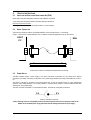
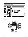
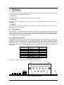
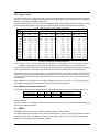
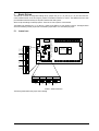
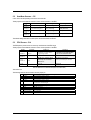
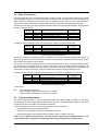
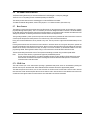
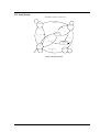
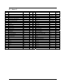
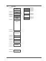
EDK2378
USER MANUAL
FOR H8S/2378
ON-CHIP FLASH MICROCONTROLLER
Preface
Cautions
1.
This document may be, wholly or partially, subject to change without notice.
2.
All rights reserved. No one is permitted to reproduce or duplicate, in any form, a part or this entire
document without Renesas Technology Europe Limited's written permission.
Trademarks
General
All brand or product names used in this manual are trademarks or registered trademarks of their respective
companies or organisations.
Specific
Microsoft, MS and MS-DOS are registered trademarks and Windows and Windows NT are
trademarks of Microsoft Corporation.
Document Information
Product Code:
D004883_11
Version:
1
Date:
14/11/2003
Copyright © Renesas Technology Europe Ltd. 2003. All rights reserved.
Website:
http://www.renesas.com/
2
1.
TABLE OF CONTENTS
1.
TABLE OF CONTENTS ............................................................................................................................................. 3
2.
START-UP INSTRUCTIONS ....................................................................................................................................... 4
2.1. INSTALLING THE EVALUATION DEVELOPMENT KIT (EDK)........................................................................... 4
2.2. SERIAL CONNECTION ....................................................................................................................................... 4
2.3. POWER SUPPLY ................................................................................................................................................ 4
3.
EDK BOARD LAYOUT ............................................................................................................................................ 5
3.1. EDK BLOCK DIAGRAM....................................................................................................................................... 5
4.
EDK OPERATION ................................................................................................................................................... 6
4.1. USER INTERFACE.............................................................................................................................................. 6
4.2. SERIAL INTERFACE........................................................................................................................................... 6
4.3. SRAM................................................................................................................................................................... 7
4.4. MEMORY MAP .................................................................................................................................................... 8
4.5. SRAM ACCESS TIMING ..................................................................................................................................... 8
4.6. LEDS.................................................................................................................................................................... 8
5.
BOARD OPTIONS .................................................................................................................................................... 9
5.1. JUMPER LINKS................................................................................................................................................... 9
5.2. USER MODE SETTINGS – CJ5........................................................................................................................ 10
5.3. EDK OPTIONS – CJ4 ........................................................................................................................................ 10
5.4. SERIAL PORT SELECTION.............................................................................................................................. 11
5.5. FLASH PROGRAMMING HEADER .................................................................................................................. 11
5.6. EXTERNAL DEBUG HEADER .......................................................................................................................... 12
5.7. BOOT CONTROL .............................................................................................................................................. 12
6.
MICROCONTROLLER HEADER CONNECTIONS ......................................................................................................... 14
6.1. HEADER J1 ....................................................................................................................................................... 14
6.2. HEADER J2 ....................................................................................................................................................... 15
7.
CODE DEVELOPMENT ........................................................................................................................................... 16
7.1. HMON ................................................................................................................................................................ 16
7.2. HEW3 WORKSPACE FOR KERNEL GENERATION AND MODIFICATION.................................................... 18
7.3. ADDITIONAL INFORMATION ........................................................................................................................... 18
3
2.
START-UP INSTRUCTIONS
2.1. INSTALLING THE EVALUATION DEVELOPMENT KIT (EDK)
Please refer to the quick start guide provided for initial installation of the EDK.
A copy of the quick start guide and other information relating to this EDK at:
http://www.eu.renesas.com/tools
Installing the EDK requires power and serial connection to a host computer.
2.2. SERIAL CONNECTION
The serial communications cable for connecting the EDK to a host computer requires 1:1 connectivity.
Figure 2-1 shows how to connect the EDK to a PC or notebook computer equipped with a nine pin D connector.
HOST
PC
EDK
3
2
5
3
2
5
FIGURE 2-1: SERIAL CONNECTION TO PC/NOTEBOOK WITH DB-9 CONNECTOR (SUPPLIED)
2.3. POWER SUPPLY
The EDK hardware requires a power supply of +5V. Since total power consumption can vary widely due to external
connections, port states, and memory configuration, use a power supply capable of providing at least 500mA at +5V DC ±
5%.
The design is specified for evaluation of the microcontroller and so does not include circuitry for supply filtering/noise
reduction, under voltage protection, over current protection or reversed polarity protection. Caution should be used when
selecting and using a power supply.
The power connector on the EDK is a 2.5mm Barrel connector. The center pin is the positive connection.
FIGURE 2-2: POWER SUPPLY CONNECTION
Caution: Existing customers using E6000 products note that the polarity of this board is opposite to that for the
E6000. Use of the E6000 power supply with this board will damage both board and power supply.
4
3.
EDK BOARD LAYOUT
The diagram shows a general layout of the EDK board.
FLASH
Programming
Power
J1
BOOT
Switch
IrDA
BOOT LED
Power LED
User1 LED
User2 LED
Testpoints
X
T
A
L
HITACHI
Microprocessor
AND
SRAM
RXDISn
DCTS
DRTS
CJ5
MD0
MD1
MD2
MD3
UPM
CSn
E10A Header
9-Way
D-Type
5V
3V3
UVcc
GND
RESn
FW
NMIn
ULED1
ULED2
PSCK
PTXD
PRXD
RX232
DTXD
DRXD
NMI
Switch
RESET
Switch
MD4
J2
CJ4
FIGURE 3-1: EDK BOARD LAYOUT
3.1. EDK BLOCK DIAGRAM
The diagram shows the connectivity of the components on the EDK board.
Boot
Reset
5V PSU
NMI
Switches
EDK specific
Control Logic
5V Supply
&
3V3 Regulator
SRAM
IrDA
Transceiver
RS232
Programming
& Comms
HITACHI
Microprocessor
On-Chip
Debug
Connector
(E10A
Header)
LEDs
User1
&
User2
Power
&
Boot
Header
Connectors
FIGURE 3-2: EDK BLOCK DIAGRAM
5
4.
EDK OPERATION
4.1. USER INTERFACE
The EDK provides three buttons for influencing the operation of the board. The purpose of each button is clearly marked next
to it. Refer to the board layout for positions (Section 3)
1.
Reset Switch
This button provides the microcontroller with a timed reset pulse of at least 250mS.
2.
Boot Switch
This button toggles the operating mode of the microcontroller. A complete description of this function is given in
section 5.7.
3.
NMI Switch
This button provides a de-bounced signal to the microcontroller for each operation of the button. There is no minimum or
maximum activation time for this button.
4.2. SERIAL INTERFACE
The serial interface on the EDK board has several functions. The serial port on the microcontroller directly supports three
wire serial interfaces. Options are provided on the board for the user to write handshaking routines using standard port pins.
Other board option links allow users to control the entry and exit from boot mode using the same handshaking signals. Refer
to section 5.4 for details on setting serial interface options.
4.2.1. CONNECTOR PIN DEFINITIONS
The EDK RS232 interface conforms to Data Communication Equipment (DCE) format allowing the use of 1-1 cables when
connected to Data Terminal Equipment (DTE) such as an IBM PC. The cable used to connect to the EDK will affect the
available board options. A fully wired cable can allow handshaking between the microcontroller and the host PC, subject to
setting the board options and the availability of suitable host software. Handshaking is not supported as standard on the
microcontroller so for normal use a minimal three-wire cable can be used. The minimum connections are unshaded in the
following table.
EDK DB9
Connector Pin
1
2
3
4
5
6
7
8
9
Signal
Host DB9
Connector Pin
No Connection
EDK Tx Host Rx
EDK Rx Host Tx
No Connection
Ground
No Connection
* EDK CTS Host RTS
* EDK RTS Host CTS
No Connection
1
2
3
4
5
6
7
8
9
TABLE 4-1: RS232 INTERFACE CONNECTIONS
* These are not connected on the EDK by default. See section 5.4 for more details.
5
4
9
3
8
2
7
1
6
FIGURE 4-1: EDK SERIAL PORT PIN NUMBERING
6
4.2.2. CRYSTAL CHOICE
The operating crystal frequency has been chosen to support the fastest operation with the fastest serial operating speeds.
The value of the crystal is 14.7456MHz. The HMON tutorial code configures the PLL control register (PLLCR) to multiply this
internally by 2 to provide a 29.4912MHz internal clock.
The following table shows the baud rates and Baud Rate Register (BRR) setting required for each communication rate using
the above default operating speed. It also confirms the resultant baud rate and the bit error rate that can be expected.
Baud Rate Register Settings for Serial Communication Rates
SMR
Setting:
Comm.
Baud
0
1
2
BRR
setting
110 invalid
300 invalid
Actual
Rate
invalid
ERR
(%)
invalid
BRR
setting
invalid
Actual
Rate
invalid
ERR
(%)
invalid
BRR
setting
invalid
invalid
invalid
invalid
invalid
invalid
1200 invalid
2400 invalid
invalid
invalid
191
1200
0.00
invalid
invalid
95
2400
4800
0.00
47
4800
3
Actual
Rate
invalid
ERR
(%)
invalid
BRR
setting
130
Actual
Rate
110
ERR
(%)
-0.07
191
300
0.00
47
1200
0.00
47
300
0.00
11
1200
0.00
23
2400
0.00
0.00
5
2400
0.00
11
4800
0.00
0.00
2
4800
0.00
4800
191
9600
95
9600
0.00
23
9600
0.00
5
9600
0.00
1
7200
-25.00
19200
47
19200
0.00
11
19200
0.00
2
19200
0.00
invalid
invalid
invalid
38400
23
38400
0.00
5
38400
0.00
1
28800
-25.00
invalid
invalid
invalid
57600
15
57600
0.00
3
57600
0.00
0
57600
0.00
invalid
invalid
invalid
115200
7
115200
0.00
1
115200
0.00
invalid
invalid
invalid
invalid
invalid
invalid
230400*
3
230400
0.00
0
230400
0.00
invalid
invalid
invalid
invalid
invalid
invalid
460800*
1
460800
0.00
invalid
invalid
invalid
invalid
invalid
invalid
invalid
invalid
invalid
TABLE 4-2 CRYSTAL FREQUENCIES FOR RS232 COMMUNICATION
* Note: The device used to convert the RS232 serial information to logic signals for the microcontroller is limited to
120kBaud. The rates above this level can only be utilised if the user provides direct logic level communications.
The user may replace the HC49/U surface mounted AT cut crystal with another of similar type within the operating frequency
of the microcontroller device. Please refer to the hardware manual for the microcontroller for the valid operating range.
Alternatively the user may fit an oscillator module – or provide an external clock source. When providing an oscillator module
or external source it is highly recommended that the load capacitors for the AT crystal are removed from the PCB. These are
physically placed within the PCB outline of the oscillator module for easy location and to ensure they are removed when
using this option.
When changing the crystal frequency the pre-loaded debugging monitor will not function. In this situation the user is
responsible for providing code to evaluate the device away from the default operating speed.
4.2.3. REMOVABLE COMPONENT INFORMATION.
This information is provided to allow the replacement of components removed from the board as described in section 4.2.2.
Component
Load Resistor (X2)*
Load capacitors (X2)
Cct. Ref
R6
C1,C2
Value
1MΩ
22pF
Rating
0805 1%
0603 10% 25V
Manufacturer
Welwyn WCR Series
AVX 0603 3 A 220 KAT
TABLE 4-3: REMOVABLE COMPONENT INFORMATION
* Normally Not Fitted
Care must be taken not to damage the tracking around these components. Only use soldering equipment designed for
surface mount assembly and rework.
4.3. SRAM
The SRAM device fitted to the board is a 4Mbit device allowing 128kx16 or 256kx8 operation.
The onboard H8S2378 microcontroller has chip select management built in. There is no external chip selection hardware
associated with this device. The SRAM is connected to Chip Select 0 (CS0), which can address the range H80000 –
HFF4000. The usable address range is H’800000 – H’BFFFF.
7
4.4. MEMORY MAP
Table 4-4 illustrates the EDK memory map for mode 4.
Section End
Section Start
Section Allocation
H’000000
H’07FFFF
H’080000
H’0BFFFF
H’0A0000
H’1FFFFF
H’200000
H’FF3FFF
H’FF4000
H’FFBFFF
H’FFC000
H’FFCFFF
H’FFD000
H’FFFBFF
H’FFFC00
H’FFFEFF
H’FFFF00
H’FFFF1F
H’FFFF20
H’FFFFFF
ROM
External SRAM
Reserved
External Address Space
On-chip RAM / External Address Space
Reserved
External Address Space
Internal I/O registers
External Address Space
Internal I/O registers
TABLE 4-4: MEMORY MAP (DEFAULT MODE 4)
4.5. SRAM ACCESS TIMING
External access timing is defined by several registers, allowing different types of devices to be addressed. The registers for
the selection of wait states and signal extensions are given below with recommended values for the EDK.
Register
ABWCR
ASTCR
WTCRBL
RDNCR
Port C DDR
Port B DDR
Port A DDR
Port G DDR
Address
FEC0
FEC1
FEC5
FEC6
FE2B
FE2A
FE29
FE2F
Recommended
Setting for EDK
0x00
0xFF
0x01
0x01
0xFF
0xFF
0x07
0x01
Function
Set all 8 memory areas to be 16 bit access
Selects bus width for memory accesses
Selects one wait state for memory accesses
Selects RDN0 as Read Strobe signal for memory area 0
Configures Port C for output of address line signals
Configures Port B for output of address line signals
Configures Port A for output of address line signals
Configures pin PG0 as CS0 (i.e. chip select for memory area 0)
TABLE 4-5: SRAM ACCESS CONTROL REGISTERS
Please refer to the hardware manual for the microcontroller for more information on these register settings.
4.6. LEDS
The EDK has four red LEDs. The function of each LED is clearly marked on the silk screen of the PCB. Please refer to the
board layout diagram for position information (Section 3).
When the board is connected to a power source the Power (PWR) led will illuminate. The Boot mode indication LED will
illuminate when the microcontroller has been placed into Boot mode. Please see section 5.7 for more details of this function.
There are two LEDs dedicated for user control these are marked USR1 and USR2. Each LED will illuminate when the port
pin is in a logical high state.
The user LEDs are connected to the following ports:
LED Identifier
USR1
USR2
Port Pin
P26
P25
Microcontroller Pin
Pin 57
Pin 56
Pin Functions on Port Pin
P26/PO6/TIOCA5/IRQ14n
P25/PO5/TIOCB4/IRQ13n
TABLE 4-6: LED PORT CONNECTIONS
8
5.
BOARD OPTIONS
The EDK has a number of configuration settings set by jumpers CJ4 (A, B, C, D) CJ5 (A, B, C, D) and zero-ohm links.
Common EDK functions can be set using the jumpers as described in sections 5.3 and 5.2. The additional zero-ohm links
provide additional features that may be required to interface with other systems.
All the Jumper link settings are three pin options. There are four sets of options on each header.
The headers are numbered from 1 to 12 with pin 1 marked on the PCB by an arrow pointing to the pin. The diagram below
shows the numbering of these jumper links and indicates jumpers fitted 1-2 for each three-pin jumper.
5.1. JUMPER LINKS
5V
3V3
UVcc
GND
Power
RESn
FW
NMIn
ULED1
ULED2
PSCK
PTXD
PRXD
RX232
DTXD
DRXD
NMI
Switch
4
1 2 3
Jumper
C
1,2,3
7
BOOT
Switch
AND
HITACHI
Microprocessor
3
RXDISn
DCTS
DRTS
CJ5
5
9-Way
D-Type
X
T
A
L
MD0
MD1
MD2
MD3
UPM
SRAM
E10A
1
1 2 3
Jumper
B
1,2,3
2
1 2
3
Jumper
A
1,2,3
BOOT LED
Power LED
User1 LED
User2 LED
RESET
Switch
J1
IrDA
MD4
FLASH
Prog ramming
6
CSn
J2
8
CJ4
9 10 11
12
1 2 3
Jumper
D
1,2,3
1
2
3
1 2
3
Jumper
A
1,2,3
4
5
6
1 2 3
Jumper
B
1,2,3
7
8
9 10 11
1 2 3
Jumper
C
1,2,3
12
1 2 3
Jumper
D
1,2,3
FIGURE 5-1: JUMPER CONFIGURATION
The following tables define each jumper and its settings.
9
5.2. USER MODE SETTINGS – CJ5
CJ5 is used to set the operating mode of the microcontroller.
These jumpers must be fitted at all times to ensure correct operation of the EDK.
Jumper
CJ 5-A
Default 2-3
CJ 5-B
Default 2-3
CJ 5-C
Default 1-2
CJ 5-D
Default 1-2
Function
Setting 1-2
Setting 2-3
User Mode Setting Bit 0
MD0 pulled High
MD0 pulled Low
User Mode Setting Bit 1
MD1 pulled High
MD1 pulled Low
User Mode Setting Bit 2
MD2 pulled High
MD2 pulled Low
User Mode Setting Bit 3
MD3 pulled High
MD3 pulled Low
TABLE 5-1: USER MODE: JUMPER SETTINGS (DEFAULT SETTINGS IN BOLD)
The default settings indicated in bold text place the microcontroller into Mode 4.
5.3.
EDK OPTIONS – CJ4
The EDK options provide access to commonly used features of the EDK range.
These jumpers must be fitted at all times to ensure correct operation of the EDK.
Jumper
Function
CJ 4-A
Default 2-3
Serial Receive
Source
CJ 4-B
Default 2-3
UPM
CJ 4-C
Default 1-2
CSn
CJ 4-D
Default 2-3
Setting 1-2
Disables the RS232 receive signal
to enable the use of the Flash
Programming Header
Enables E10A Interface
Setting 2-3
Enables the RS232 receive signal.
The Flash Programming Header*
must not be used in this state.
Disables E10A Interface
SRAM device enabled: Device
selected by microcontroller.
SRAM device Disabled:
Device permanently de-selected.
(DEFAULT)
-
Not Used
Not Used
TABLE 5-2: BOARD OPTION: JUMPER SETTINGS (DEFAULT SETTINGS IN BOLD)
*See section 5.5
The following table lists the connections to each jumper pin.
Pin
1
2
3
4
5
Net Name
UVCC
RXDISn
No Connection
UVCC
UPM
6
7
8
9
10
11
12
No Connection
PG0
CSn
No Connection
No Connection
No Connection
No Connection
Description
Microcontroller Supply Voltage
Disable Flash Header functions. Pulled low. (Enables RX232)
No Connection
Microcontroller Supply Voltage
CPLD Controlled option to set Flash Write (FW). Pulled low.
E10A Enable / Disable Signal.
No Connection
Microcontroller CSn(0) signal
SRAM CSn signal
No Connection
No Connection
No Connection
No Connection
10
5.4. SERIAL PORT SELECTION
The programming serial port is connected to the RS232 connector by default. This allows direct programming of the EDK
using the supplied software tools. A secondary serial port is available on the microcontroller and can be connected to the
RS232 connector by changing some board option links. The additional port option allows the user to write messages or
connect to other devices via the serial port while programming support is provided by the Flash programming header.
The following surface mount, zero-ohm link settings are fitted by default and connect the RS232 header to the programming
serial port of the microcontroller.
Zero-ohm
Link ID
CR20
CR23
CR19
CR22
Default
Fitted
Fitted
Not Fitted
Not Fitted
Function
Transmit data from EDK
Receive data to EDK
Alternate Transmit data from EDK
Alternate Receive data to EDK
Microcontroller
Port Pin
P31
P33
P23
P24
TABLE 5-3: OPTION LINKS – DEFAULT SETTINGS
To enable the use of this alternate port the user must change the settings to those in the following table.
Zero-ohm
Link ID
CR20
CR23
CR19
CR22
Default
Not Fitted
Not Fitted
Fitted
Fitted
Function
Transmit data from EDK
Receive data to EDK
Alternate Transmit data from EDK
Alternate Receive data to EDK
Microcontroller
Port Pin
P31
P33
P23
P24
TABLE 5-4: OPTION LINKS – ALTERNATE SERIAL PORT
The user may implement a handshaking protocol on the EDK. This is not supported with the software tools supplied. To
support this option two spare port pins have been allocated on the microcontroller. Using these port pins the CTS and RTS
lines of the host serial interface can be controlled.
The user may also control the operation of the board via the same handshaking lines. This is not supported with the software
tools supplied but may be written by the user. Using the CTS line the user may simulate pressing the boot button, see
section:5.7. This will cause the EDK to swap into and out of Boot mode on each low-level activation of CTS. Feedback of the
current mode is provided on the RTS line. A high level indicates boot mode and a low level indicates user mode.
The following settings are made by default, and ensure that there are no conflicts on unnecessary microcontroller pins.
Zero-ohm
Link ID
CR12
CR7
CR16
CR13
Default
Not Fitted
Not Fitted
Not Fitted
Not Fitted
Function
Mode State out from EDK
Change Mode request to EDK
Alternate RTS232 – Ready to send – from EDK
Alternate CTS232 – Clear to send – to EDK
Microcontroller
Port Pin
N/A (From CPLD*)
N/A (From CPLD*)
P22
P21
TABLE 5-5: OPTION LINKS – SERIAL PORT CONTROL
* See section 5.7
Note:
These setting pairs are exclusive:
If CR12 and CR7 are fitted; CR16 and CR13 must not be fitted.
If CR16 and CR13 are fitted; CR12 and CR7 must not be fitted.
5.5. FLASH PROGRAMMING HEADER
The Flash Programming header is used with the Renesas Flash Debug Module (FDM). The FDM is a USB based
programming tool for control and programming of Renesas microcontrollers, available separately from Renesas. This header
provides direct access for the FDM to control the EDK microcontroller.
To utilise this header the user must make the following changes to the board configuration.
1.
Disable the RX232 signal from the RS232 transceiver.
Jumper link CJ4-A is provided for this purpose. Please refer to section 5.3.
2.
Disable the UPM jumper (which enables the E10A) by setting CJ4-B to 2-3. Refer to section 5.3.
Caution: Do not operate the board with the user mode jumpers removed and the FDM disconnected, as the
microcontroller mode pins will float to an indeterminate state. This may damage the microcontroller device.
11
5.6. EXTERNAL DEBUG HEADER
The External debug header may be used with the Renesas E10A Debugger or a third party debugger.
The E10A is an on-chip debug emulator available separately from Renesas.
This header provides direct access for the debugger to control the EDK microcontroller.
To enable the external debug header, set the CJ4-B jumper to 1-2 to enable emulation. (See section 5.3).
5.7. BOOT CONTROL
The method for placing the microcontroller device into Boot mode for reprogramming has been incorporated into a complex
programmable logic device (CPLD). This is not necessary for most user designs but allows a measure of increased flexibility
for the EDK designs. Mode transitions including boot mode transitions only require the reset to be held active while the mode
settings are presented. On releasing reset the microcontroller will be in the required mode.
The logic design detects a power up event and provides a timed reset pulse to guarantee the reset of the device. At the end
of the rest pulse the processor will be placed in user mode and any code in the device will execute.
During user mode the NMI button can be pressed at any time. This will provide a single de-bounced NMI interrupt to the
device.
Pressing the boot button will cause the boot mode controller to reset the device and, during the reset period, present the
required mode settings to start the device in boot mode. At the end of the reset period the boot mode settings will have been
latched into the device, which will then be ready to accept a boot mode connection via the RS232 interface or the flash
programming header. Pressing the boot button during a normal reset will not cause the EDK to enter boot mode.
The boot mode settings are fixed at mode 3. The required mode settings are made using a tri-state capable buffer.
Note:
The boot control device is programmed to support all possible EDK products.
For this reason the reset pulse is over 500ms. Repetitive activation of either the Boot or Reset buttons will restart
the reset timer and extend the reset period. Pressing the boot button within the 500mS period of a reset will not
cause the board to enter boot mode.
5.7.1. CPLD CODE
The code is based upon a four state machine providing a guaranteed reset period, which can be extended by holding the
relevant control input in the active state. When released the timer will extend the reset for approximately 500mS.
The states are split into two functions, one for User mode and one for Boot mode. The first state of each is used to hold the
reset line active. When the timer expires then the second state is used to hold the device in the selected mode and wait for
an external control signal to either move back into the user reset state or into the boot reset state.
12
5.7.2. STATE DIAGRAM
Boot Mode Controller : Positive Logic
(CTS+BootSw) . /Res
Waiting
Boot
/Res . Boot
Res
Reset Timer
/Res
ResSw . /Res
Res
/Res
/Res . Reset
Clocked Transitions
using NE555
(All solid transition
lines)
Reset
(BootSW + ResSw + CTS)
. /Res
BootWaiting
Async
FIGURE 5-2: CPLD STATE DIAGRAM
13
6.
MICROCONTROLLER HEADER CONNECTIONS
The following table lists the connections to each or the headers on the board.
6.1. HEADER J1
Pin
No
1
3
5
7
9
11
13
15
17
19
21
23
25
27
29
31
33
35
37
39
41
43
45
47
49
51
53
55
57
59
61
63
65
67
69
71
Function
Vss
PLLVss
PLLVcc
PF5/RDn
PF3/LWRn
PF1/IRQ14n/UCASn/DQMU
P62/TEND0n/TMCIO/IRQ10n
P60/DREQ0n/TMRIO/IRQ8n
PD6/D14
PD4/D12
PD2/D10
PD0/D8
PE7/D7
PE6/D6
PE4/D4
PE2/D2
PE0/D0
P85/IRQ5n/SCK3/EDACK3
P83/IRQ3n/RxD3/ETEND3
P26/P06/TIOCA5/IRQ14n
P24/PO4/TIOCA4/RxD4/IRQ12n
P22/PO2/TIOCC3/IRQ10n
P20/PO0/TIOCA3/IRQ8n
P17/PO15/TIOCB2/TCLKD/EDRAK3n
P15/PO13/TIOCB1/TCLKC
P13/PO11/TIOCD0/TCLKB
P11/PO9/TIOCB0
Vcl*
WDTOVFn
PH2/CS6n/IRQ6n
PH0/CS4n/RAS4n/WEn
P81/IRQ1n/TxD3/EDREQ3n
PA7/A23/IRQ7n
PA5/A21/IRQ5n
PA3/A19
Vss
EDK Symbol
GND
NC_J1_03
NC_J1_05
PF5
PF3
PF1
P62
P60
PD6
PD4
PD2
PD0
PE7
PE6
PE4
PE2
PE0
P85
P83
ULED1
DRXD
DRTS
P20
P17
P15
P13
P11
UVcc
WDTOVFn
PH2
PH0
P81
PA7
PA5
PA3
GND
J1
Device
pin
95
93
91
89
87
85
83
81
79
77
75
73
71
69
67
65
63
61
59
57
55
53
51
49
47
45
43
41
39
37
35
33
31
29
27
25
Pin
No
2
4
6
8
10
12
14
16
18
20
22
24
26
28
30
32
34
36
38
40
42
44
46
48
50
52
54
56
58
60
62
64
66
68
70
72
Function
PF7/Φ
RESn
PF6/ASn
PF4/HWRn
PF2/IRQ15n/LCASn/DQML
PF0/WAITn
P61/DREQ1n/TMRI1/IRQ9n
PD7/D15
PD5/D13
PD3/D11
PD1/D9
Vcc
Vss
PE5/D5
PE3/D3
PE1/D1
DCTL
P84/IRQ4n/EDACK2
P27/PO7/TIOCB5/IRQ15n
P25/PO5/TIOCB4/IRQ13n
P23/PO3/TIOCD3/TxD4/IRQ11n
P21/PO1/TIOCB3/IRQ9n
Vss
P16/PO14/TIOCA2/EDRAK2n
P14/PO12/TIOCA1
P12/PO10/TIOCC0/TCLKA
P10/PO8/TIOCA0
NMI
PH3/CS7n/IRQ7n/Oen/CKE
PH1/CS5n/RAS5n/SDRAMΦ
P82/IRQ2n/ETEND2n
EMLE
PA6/A22/IRQ6n
PA4/A20/IRQ4n
PA2/A18
PA1/A17
EDK Symbol
PF7
RESETn
PF6
PF4
PF2
PF0
P61
PD7
PD5
PD3
PD1
UVcc
GND
PE5
PE3
PE1
DCTL
P84
P27
ULED2
DTXD
DCTS
GND
P16
P14
P12
P10
NMIn
PH3
PH1
P82
FW
PA6
PA4
PA2
PA1
* Pin 41 is Vcl for H8S/2378 and VCC for H8S/2377
14
Device
pin
94
N\A
90
88
86
84
82
80
78
76
74
72
70
68
66
64
62
60
58
56
54
52
50
48
46
44
42
40
38
36
34
32
30
28
26
24
6.2. HEADER J2
Pin
No
1
3
5
7
9
11
13
15
17
19
21
23
25
27
29
31
33
35
37
39
41
43
45
47
49
51
53
55
57
59
61
63
65
67
69
71
Function
XTAL
Vcc
NC
Vss
P63/TEND1n/TMCI1/IRQ11n
P65/DACK1n/TMO1/IRQ13n
PG1/CS1n
PG3/CS3n/RAS3n/CASn
Vref
P41/AN1
P43/AN3
P45/AN5
P47/AN7/DA1
P91/AN9
P93/AN11
P95/AN13/DA3
P97/AN15/DA5
PG4/BREQ0n
PG6/BREQn
P51/RxD2/IRQ1n
P53/ADTRGn/IRQ3n
P34/SCK0/SCK4/SDA0
P32/RxD0/IrRxD/SDA1
P30/TxD0/IrTxD
MD1
Vss
Vcc
PC1/A1
PC3/A3
Vss
PC6/A6
PB0/A8
PB2/A10
Vss
PB5/A13
PB7/A15
EDK Symbol
CON_XTAL
UVcc
NC_J2_05
GND
P63
P65
PG1
PG3
CON_VREF
P41
P43
P45
P47
P91
P93
P95
P97
PG4
PG6
P51
P53
P34
P32
P30
MD1
GND
Uvcc
PC1
PC3
GND
PC6
PB0
PB2
GND
PB5
PB7
J2
Device
pin
96
98
100
102
104
106
108
110
112
114
116
118
120
122
124
126
128
130
132
134
136
138
140
142
144
2
4
6
8
10
12
14
16
18
20
22
Pin
No
2
4
6
8
10
12
14
16
18
20
22
24
26
28
30
32
34
36
38
40
42
44
46
48
50
52
54
56
58
60
62
64
66
68
70
72
Function
EXTAL
Vcc
NC
STBYn
P64/DACK0n/TMO0/IRQ12n
PG0/CS0n
PG2/CS2n/RAS2n/RASn
Avcc
P40/AN0
P42/AN2
P44/AN4
P46/AN6/DA0
P90/AN8
P92/AN10
P94/AN12/DA2
P96/AN14/DA4
Avss
PG5/BACKn
P50/TxD2/IRQ0n
P52/SCK2/IRQ2n
P35/SCK1/SCL0/0En/CKE
P33/RxD1/SCL1
P31/TxD1
MD0
MD2
P80/IRQ0n/EDREQ2n
PC0/A0
PC2/A2
PC4/A4
PC5/A5
PC7/A7
PB1/A9
PB3/A11
PB4/A12
PB6/A14
PA0/A16
EDK Symbol
CON_EXTAL
UVcc
NC_J2_06
STBYn
P64
PG0
PG2
CON_AVCC
P40
P42
P44
P46
P90
P92
P94
P96
CON_AVSS
PG5
P50
P52
PSCK
PRXD
PTXD
MD0
MD2
P80
PC0
PC2
PC4
PC5
PC7
PB1
PB3
PB4
PB6
PA0
15
Device
pin
97
99
101
103
105
107
109
111
113
115
117
119
121
123
125
127
129
131
133
135
137
139
141
143
1
3
5
7
9
11
13
15
17
19
21
23
7.
CODE DEVELOPMENT
7.1. HMON
7.1.1. MODE SUPPORT
The HMON library is built to support Advanced Expanded Mode only. The Device supports only Mode 4.
7.1.2. BREAKPOINT SUPPORT
The monitor has no PC Break Controller, therefore no breakpoints can be located in ROM. Code located in RAM may have
multiple breakpoints limited only by the size of the On-Chip RAM.
7.1.2.1.CODE LOCATED IN RAM
Double clicking in the breakpoint column in the code sets the breakpoint. Breakpoints will remain unless they are double
clicked to remove them.
7.1.3. HMON CODE SIZE
HMON is built along with the debug code. Certain elements of the HMON code must remain at a fixed location in memory.
The following table details the HMON components and their size and location in memory. For more information, refer to the
map file when building code.
Section
Description
Start Location
Size
(H’bytes)
RESET_VECTOR
HMON Reset Vector (Vector 0)
Required for Startup of HMON
Trap Vectors (Vector 8, 9, 10, 11)
Required by HMON to create Trap Breakpoints in RAM
HMON Break Controller (Vector 27)
Required by HMON to create Breakpoints in ROM
HMON Serial Port Vectors (Vector 80, 81, 82, 83)
Used by HMON when EDK is configured to connect to the
default serial port.
HMON Code
HMON Constant Data
HMON Uninitialised data
FDT User Mode Kernel.
This is at a fixed location and must not be moved. Should the
kernel need to be moved it must be re-compiled.
Pointer used by HMON to point to the start of user code.
H’ 000000000
4
H’ 00000020
10
H’ 0000006C
4
H’ 00000170
C
H’ 00005000
H’ 000072FA
H’ 00FF4432
H’ 0001000
22FA
148
20F
D03
H’ 00002000
4
TRAP_VECTORS
HW_BREAK_VECTORS
SCI_VECTORS
PHMON
CHMON
BHMON
FDTUserModeMicroKernel
CUser_Vectors
16
7.1.4.
MEMORY MAP
H'00000000
Vectors
RESET Vector
TRAP Vectors
H'00001000
H'00001119
H'00002000
H'00002003
H'00000000
H'00000003
H'00000020
H'0000002F
FDTUserModeMicr
oKernel
HW Break Vector
H'0000006C
H'0000006F
SCI Vectors
H'00000170
H'0000017B
CUser_Vectors
H'00005000
PHMON
CHMON
H'00007441
On-Chip FLASH
ROM
H'0007FFFF
H'00FFB000
On-Chip RAM
H'00FF4432
BHMON
H'00FF4640
H'00FFA000
H'00FFA1FF
Stack
H'00FFBFFF
H'00FFFC00
H'00FFFF00
H'00FFFF20
Internal I/O
REGISTERS
Internal I/O
REGISTERS
H'00FFFFFF
17
7.1.5.
BAUD RATE SETTING
HMON has initially set to connect at 115200Baud. Should the user wish to change this, the value for the BRR in
HMONserialconfiguser.c will need to be changed and the project re-built. Please refer to the HMON User Manual for further
information.
7.1.6.
INTERRUPT MASK SECTIONS
HMON has an interrupt priority of 6. The serial port has an interrupt priority of 7. Modules using interrupts should be set to
lower than this value (6 or below), so that serial communications and debugging capability is maintained.
7.2. HEW3 WORKSPACE FOR KERNEL GENERATION AND MODIFICATION
This CD provides a Hew3 workspace for re-creating the user kernels. This potentially allows the user to rebuild the user
mode kernel files uGenu.cde and 2378F.mot if required. This would be the case if, for example, the crystal was replaced with
that of a differing value.
The HEW3 kernel workspace is located under the FDT3.1 installation in the 1_0_00.edk folder and is called “2378F”. The
workspace contains two build configurations ‘BinaryForHMON” and “FDT_USER_MOT”. The FDT_USER_MOT configuration
builds the file “2378F.mot”. This can be included in an FDT project and used to program the device in both user and user
boot modes. The BinaryForHMON build configuration generates the binary uGenu.cde file. This is used by HMON to
program the device in user mode.
The workspace created by the EDK project generator stores this file on the device chip at an address given by in the section
“FDTUserModeMicroKernel”. This must not be moved from the default memory location. The user can view the
FDTUserModeMicroKernel section address location in Hew3 by going to ‘Options’ -> Toolchain, selecting ‘Link/Library’
Tab in the window that appears and then in the drop down menu next to Category and selecting ‘section’.
If the user wishes to rebuild the kernels it is strongly recommended that both configurations are built at the same time. This
will reflect any source or workspace changes in both 2378F.mot and uGenu.cde files. Multiple builds can be performed
automatically in Hew3 by going to Build -> Build Multiple… and in the window that opens ticking both build configurations.
The box ‘Build All’ should then be pressed to initiate builds of both uGenu.cde and 2378F.mot files. This should be done
each time a new build of the kernels is required. The generated uGenu.cde file will then need to be copied into the users
target code workspace overwriting the existing file.
7.3. ADDITIONAL INFORMATION
For details on how to use High-performance Embedded Workshop (HEW), with HMON, refer to the HEW manual available
on the CD or from the web site.
For information about the H8S/2378 series microcontrollers refer to the H8S/2378 Series Hardware Manual
For information about the H8S/2378 assembly language, refer to the H8S Series Programming Manual
Further information available for this product can be found on the Renesas web site at:
http://www.eu.renesas.com/tools
General information on Renesas Microcontrollers can be found at the following URLs.
Global:
http://www.renesas.com/
18