1
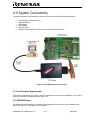
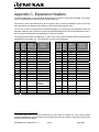
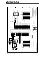
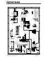
User
Powerful Processors – Easy to Use™
SKP38024
StarterKit Plus
User’s Manual
Rev. 1.0
April 2006
www.renesas.com
Table of Contents
1.0 Introduction ............................................................................................................................................. 4
2.0 Contents of Product Package................................................................................................................. 5
2.1. SKP38024 QuickStart Kit Item List.................................................................................................... 5
2.1.1. CD-ROM...................................................................................................................................... 5
3.0 Limited Guarantee and Support ............................................................................................................. 6
4.0 System Connectivity ............................................................................................................................... 7
4.1. Host Computer Requirements ........................................................................................................... 7
4.2. SKP38024 Board ............................................................................................................................... 7
4.3. E8 Debugger...................................................................................................................................... 8
4.4. Software Development Tools ............................................................................................................ 8
4.4.1. HEW (High-performance Embedded Workshop)........................................................................ 8
4.4.2. H8S, H8/300 Evaluation Version C Compiler.............................................................................. 8
4.4.3. HEW Debug Interface ................................................................................................................. 8
4.4.4. Renesas AutoUpdater ................................................................................................................. 8
4.4.5. Documentation, Sample Projects and Project Generators ......................................................... 8
5.0 Hardware ................................................................................................................................................ 9
5.1. SKP38024 Board ............................................................................................................................... 9
5.2. SKP38024 Board Block Diagram .................................................................................................... 10
5.3. H8/38024 Group of MCUs ............................................................................................................... 10
5.4. SKP38024 Functional Blocks .......................................................................................................... 10
5.4.1. Boot/Reset Controller ................................................................................................................ 11
5.4.2. Switches .................................................................................................................................... 11
5.4.3. LEDs.......................................................................................................................................... 11
5.4.4. RS232 Serial Interface .............................................................................................................. 11
5.4.5. LCD ........................................................................................................................................... 12
5.4.6. SKP38024 I/O Ports .................................................................................................................. 13
5.5. Flash Programming Connector........................................................................................................ 13
5.6. E10T Debug Connector................................................................................................................... 13
5.7. SKP38024 Board Jumper Configuration ......................................................................................... 13
5.7.1. CJ5: User Mode Settings .......................................................................................................... 14
5.7.2. CJ4: RS232 Receive Enable..................................................................................................... 14
6.0 System Operation & Limitations ........................................................................................................... 16
6.1. Kernel (ROM Monitor) Introduction.................................................................................................. 16
6.2. Pin and Peripheral Limitations......................................................................................................... 16
6.3. Memory Map.................................................................................................................................... 17
6.4. Low-Power Modes ........................................................................................................................... 17
6.5. Limitations on Interrupts .................................................................................................................. 17
6.6. Sleep Instruction Limitations............................................................................................................ 18
6.7. User Program’s Real-Time Capability ............................................................................................. 18
6.8. Watchdog Timer .............................................................................................................................. 18
7.0 SKP38024 Board Specifications........................................................................................................... 19
7.1. Hardware Specifications.................................................................................................................. 19
7.2. Power Supply Requirements ........................................................................................................... 19
7.3. Operating Environment.................................................................................................................... 20
Appendix A. Troubleshooting Guide........................................................................................................... 21
A.1 USB Driver Problems ....................................................................................................................... 21
A.2 Debugging Problems........................................................................................................................ 21
A.2.1 Erratic Debug Behavior.............................................................................................................. 21
A.2.2 Can’t Connect to Target............................................................................................................. 22
A.2.3 Issues that May Arise During Debug Operations ...................................................................... 22
Appendix B. Reference Manuals ................................................................................................................ 24
Appendix C. Expansion Headers................................................................................................................ 25
SKP38024 User’s Manual Rev 1.0
April 2006
Appendix D. Board Schematic.................................................................................................................... 27
Appendix E. SKP38024 Printed Circuit Board............................................................................................ 32
Appendix F. Other Resources .................................................................................................................... 33
SKP38024 User’s Manual Rev 1.0
3/ 33
April 2006
1.0 Introduction
The SKP38024 StarterKit Plus (SKP) is a low-cost development environment for evaluating Renesas
software development tools and the H8/38024 group, which is part of the H8/300L High Speed series of
microcontrollers. Micro controller units (MCU) of the H8/38024 group are equipped with a LCD (Liquid
Crystal Display) controller/driver.
The kit comes with a complete software development tool chain for Renesas MCUs, including Highperformance Embedded Workshop (HEW), which includes Integrated Development Environment (IDE),
Graphical User Interface (GUI) and Software Debugger; H8S-H8/300 C-compiler, assembler and linker;
and the E8 In-Circuit Debugger (ICD).
A real-time, source-level debug environment is implemented using the HEW4 software debug interface in
conjunction with the E8 ICD hardware. The E8 also allows for programming H8/300 devices within HEW.
The E8 and firmware provide a convenient USB (Universal Serial Bus) interface between the SKP38024
board and the host PC. This interface reduces resource requirements on the H8/38024 MCU, allows
faster code downloads, and can be used with many other Renesas Flash MCUs, SKPs, and user target
boards.
SKP38024 User’s Manual Rev 1.0
4/ 33
April 2006
2.0 Contents of Product Package
This section describes the contents of the SKP38024 product package. When unpacking your SKP38024,
please check to see that all items listed below are included.
2.1. SKP38024 QuickStart Kit Item List
Table 2-1 lists the items included in the SKP38024.
Table 2-1 SKP38024 Item List
Item Name
SKP38024 Board
E8 Debugger
Quantity
1
1
6’ Mini USB Cable
SKP CD-ROM
1
1
SKP38024 Quick Start Guide
1
Promotional CD
1
Remarks
H8/38024 SKP Board
HEW Debugger / USB Programmer Interface Device
(includes 14-pin ribbon cable)
Connects E8 Debugger to Host PC
Auto-install program
HEW (IDE & debugger)
H8S, H8/300 C-compiler, assembler, and linker
USB drivers
Manuals
Tutorials
Sample programs
Assists user in installing the tools and launching them
for the first time.
Evaluation versions of third-party tools may be included
with the kit
2.1.1. CD-ROM
The CD-ROM contains the electronic manuals and software necessary for developing programs. Your
computer must have a web browser — like Mozilla Firefox, Netscape® Browser or Microsoft® Internet
Explorer — to view the help files, and Adobe® Acrobat® Reader® to view the manuals.
Insert the enclosed CD into your computer; the installer should auto-start. The installer program will
create C:\Renesas and C:\Workspace folders on your machine. Documentation, sample code,
and other SKP-related files are in the C:\Renesas folder. HEW is installed in the
C:\Program Files\Renesas folder by default.
If the installer program does not start automatically, browse to the CD’s root folder and double-click
on SKP-Installer.exe to start the installation.
SKP38024 User’s Manual Rev 1.0
5/ 33
April 2006
3.0 Limited Guarantee and Support
Renesas Technology America, Inc., warrants the SKP38024 to be free from component or assembly
defects for a period of 180 days from the date of purchase. Settlement is limited to repair or replacement
of the product only. Renesas Technology America, Inc., does not assume any liability arising out of the
application or use of any product, circuit or procedure described herein. No other liability or warranty
applies, expressed or implied. Software warranty is limited to replacement of the CD only. While every
attempt has been made to ensure accurate documentation, Renesas Technology America, Inc., cannot
be held responsible for errors or omissions, and reserves the right to make changes without prior notice.
SKP38024 User’s Manual Rev 1.0
6/ 33
April 2006
4.0 System Connectivity
The following hardware and software products are required to use the SKP38024 QuickStart Kit.
•
•
•
•
•
•
Host Computer (supplied by user)
SKP38024 Board
E8 Debugger
Target Cable
Mini USB cable
Software Tools (HEW IDE, Compiler/Linker) installed on host computer
Figure 4-1: SKP38024 System Connectivity
4.1. Host Computer Requirements
The minimum requirement to be able to use the software that comes with the SKP38024 is a PC with a
USB port and Microsoft Windows 98, Me, 2000, or XP.
4.2. SKP38024 Board
The SKP38024 board provides an evaluation and development environment for the H8/38024 group of
MCUs. See section “5.0 Hardware” for more details.
SKP38024 User’s Manual Rev 1.0
7/ 33
April 2006
4.3. E8 Debugger
The E8 provides a plug-and-play debugging and programming interface to the H8/38024 Evaluation
Board via the host computer’s Universal Serial Bus (USB). The USB port also provides power to the
H8/38024 board and E8 thereby eliminating the need for an external power supply. The E8 can be used
also to debug code on a user’s target board; see the “E8 Emulator…Notes for H8/38024” available from
the Start menu (Start > (All) Programs > Renesas > SKP38024 > All Manuals and Documents).
4.4. Software Development Tools
The installer program installs all the development tools. For details on installation, see the QuickStart
Guide or instructions in Appendix A of this manual. A brief description of all the included tools follows.
Please refer to the individual tool manuals for detailed information.
4.4.1. HEW (High-performance Embedded Workshop)
HEW provides a Graphical User Interface (GUI) that integrates the software development tools and
includes the C-compiler, assembler, linker, debugger and editor.
4.4.2. H8S, H8/300 Evaluation Version C Compiler
The evaluation version of the H8S, H8/300 C-compiler is provided with the same functionality as the
commercial version except that link size will be restricted to 64 kBytes after 60 days from when you
begin using the compiler. Contact your local sales representative if you wish to purchase a full license.
4.4.3. HEW Debug Interface
HEW communicates with a kernel (i.e. a ROM monitor program) on the target MCU through the E8
Debugger. This debug interface provides a highly efficient evaluation environment. Features include:
•
•
•
•
•
•
Source-level debugging for assembly and C language
Source editing in debug window
Single-step command
2 hardware breakpoints* (events): 1 address and 1 data breakpoint.
Up to 255 software breakpoints
C variable “watch” window
*Note: The number of breakpoints will vary depending on the Flash MCU used.
4.4.4. Renesas AutoUpdater
Included with HEW 4.0 and later is the Renesas AutoUpdater utility. This utility can be configured to
search our website (or your server) automatically for updates of the Renesas tools installed on your
PC.
4.4.5. Documentation, Sample Projects and Project Generators
The SKP includes a full set of user documentation, sample projects, and project generators (a project
generator is a template to create a project for a specific target). After installing the CD, the sample
projects can be found in the C:\Renesas\SKP38024\sample_code folder. Documentation can be
browsed by using the “Manual Navigator” from the Start menu (Start > (All) Programs > Renesas >
SKP38024 > All Manuals and Documents).
SKP38024 User’s Manual Rev 1.0
8/ 33
April 2006
5.0 Hardware
5.1. SKP38024 Board
Figure 5-1 shows the SKP38024 Board with major components identified.
Figure 5-1: SKP38024 Board
SKP38024 User’s Manual Rev 1.0
9/ 33
April 2006
5.2. SKP38024 Board Block Diagram
The SKP38024 board incorporates an HD64F38024 (H8/38024) in an 80-pin QFP package from the
H8/38024 group of microcontrollers, designated as U1.
Figure 5-2 shows the SKP38024 block diagram.
Figure 5-2: SKP38024 Block Diagram
5.3. H8/38024 Group of MCUs
The H8/38024 group of 16-bit single-chip Flash microcontrollers (MCU) is part of the H8/300L High Speed
Family. The hardware and software manuals for the H8/38024 group of microcontrollers can be found in
the C:\Renesas\SKP38024\Docs folder on your PC or from the Start menu (Start > (All) Programs >
Renesas > SKP38024 > All Manuals and Documents) after SKP software installation.
5.4. SKP38024 Functional Blocks
The SKP38024 board’s main components include an H8/38024 single-chip microcontroller, a Boot/Reset
controller, RS232 serial port, and a four-digit direct-drive LCD.
SKP38024 User’s Manual Rev 1.0
10/ 33
April 2006
5.4.1. Boot/Reset Controller
The Boot/Reset controller IC CU6 contains the decoding necessary to place the SKP38024 board into
Boot mode and to reset the MCU with a timed pulse. CU6 also acts as input for the three
pushbuttons: Reset, Boot and NMI. It controls the status of the Boot LED and inverts the pin signals
P3_1 and P3_2 coming from the MCU to control the User LEDs USR1 and USR2.
5.4.2. Switches
The SKP38024 provides three pushbuttons to control the operation of the board. Each button is
marked clearly on the PCB’s silkscreen.
Reset Switch
Pressing this button (CSW2) applies a timed reset pulse of at least 250ms to the microcontroller.
Boot Switch
Pressing the Boot Switch (CSW3) triggers the Boot/Reset Controller to generate the necessary
signaling to switch the microcontroller into Boot Mode. In Boot Mode, the MCU’s Flash memory can
be programmed via the serial port with the Flash Development Toolkit (FDT) software (not included
with this kit).
When using the included E8 Debugger to program the Flash, no user intervention is required to put
the MCU into Boot Mode.
NMI Switch
The NMI switch, CSW1, has no function on this board; the H8/38024 MCU does not have an NMI pin.
5.4.3. LEDs
The SKP38024 has four red LEDs. The function of each LED is marked clearly on the silkscreen of
the PCB. Please refer to the board layout diagram in Appendix D for position information.
When the board is connected to a power source, the Power (PWR) LED will illuminate. The Boot
Mode indication LED will illuminate when the microcontroller has been placed into Boot Mode by
pressing the Boot Mode switch.
Two LEDs dedicated for user control are marked USR1 and USR2. Each LED will illuminate when the
port pin is in a logical high state.
The user LEDs are controlled by the following pins:
Table 5-1: LED Pin Connections
LED
MCU Pin
USR1
USR2
P3_1/MOFL
P3_2/MOFH
QFP80 Package
Pin
62
63
5.4.4. RS232 Serial Interface
The serial RS232 transceiver CU3 is connected to the MCU’s on-chip UART. It is used to program
the board’s on-chip Flash memory via a PC’s serial port using the FDT software (not included with
SKP38024 User’s Manual Rev 1.0
11/ 33
April 2006
this kit). Your own code may utilize the RS232 interface to communicate with a PC or other terminal
hardware. Optional configuration settings on the board allow you to implement handshake signaling
using standard port pins.
By default, CTS and RTS are not connected to any MCU pins. If you want to use hardware
handshaking, you have to place 0Ω resistors in positions CR19 and CR22, and your code has to
process the CTS and RTS signals in software. See the schematics for details.
The SKP38024 RS232 interface conforms to Data Communication Equipment (DCE) format allowing
the use of 1-1 cables when connected to Data Terminal Equipment (DTE) such as a PC. The cable
used to connect to the SKP38024 will affect the available board options. A fully wired cable can allow
handshaking between the microcontroller and the host PC, subject to setting the board options and
the availability of suitable host software. Handshaking is not supported as standard on the
microcontroller, so normally a minimal three-wire cable can be used. The minimum connections are
shaded in the following table.
Table 5-2: RS232 Interface Connections
DB9
Connector Pin
1
2
3
4
5
6
7
8
9
SKP38024
Signal
No connection
Tx
Rx
No connection
Ground
No connection
CTS
RTS
No connection
Host (PC) Signal
No connection
Rx
Tx
No connection
Ground
No connection
RTS
CTS
No connection
Figure 5-3: DB9 Connector Pinout
5.4.5. LCD
The supplied LCD is a Varitronix VI-422-DPRC (direct-drive 4 digits). The two ‘common’ pins and the
‘colon’ symbol of the VI-422 LCD are connected to COM1 of the LCD controller.
SKP38024 User’s Manual Rev 1.0
12/ 33
April 2006
An alternative LCD footprint is available on the SKP38024 board for a VIM-503-DP-RC-LV LCD
(3-way multiplexed 4.5 digit).
To allow the use of 4-way multiplexed LCDs that require four common pins, COM4 from the
H8/38024F is routed to pin 16 on the VIM-503 footprint, which is a ‘no connect’ for this LCD.
The following are sample LCD controller register settings:
Table 5-3: LCD Register Settings
Register
LPCR
Action
OR with 08h (VI-422)
OR with 88h (VIM503)
LCR
OR with FCh
LCR2
CKSTPR2
AND with 00h
OR with 01h
Comment
Static duty cycles (COM1 used); all ports are LCD
segment I/Os.
1/3 duty cycle (COM1-3 used); all ports are LCD segment
I/Os (could use spares as port pins if configured
accordingly).
Turn on LCD supply, cont/driver & display RAM data;
clock = sys/32.
Use waveform A.
Clear LCD module standby mode in module stop register.
5.4.6. SKP38024 I/O Ports
All of the H8/38024 MCU’s pins are accessible via expansion headers J1 and J2. See Appendix C
Expansion Headers for details.
If you reconfigure the SKP38024 I/O ports, pull-up resistors may be required for proper operation in
some configurations.
When you connect external analog signals to the SKP38024, make sure that you also connect the
MCU’s analog voltage supply and reference pins to the appropriate voltage levels. AGND and AVcc
are by default connected to digital Vcc and GND via removable 0Ω resistors, R10 and R13. By
removing R10 and R13 and installing 0Ω resistors in locations R9 and R12, you can apply an analog
supply voltage different from the digital supply via the expansion header.
5.5. Flash Programming Connector
The Flash Programming Header (CJ3) is for use with legacy programming tools. Do not connect your E8
debugger to this connector.
5.6. E10T Debug Connector
Connector J3, labeled E10T on the PCB’s silkscreen, is for connecting the E8 In-Circuit
Debugger/Programmer that is included with your Starter Kit. See Figure 4-1: SKP38024 System
Connectivity.
5.7. SKP38024 Board Jumper Configuration
The SKP38024 has a number of configuration settings set by jumpers CJ4 (A, B, C, D) CJ5 (A, B, C, D)
and 0Ω links. Common SKP38024 functions can be set using the jumpers as described in sections 5.7.1
and 5.7.2.
Zero-ohm links provide additional features that may be required to interface with other systems.
All the Jumper link settings are three-pin options. There are four sets of options on each header.
SKP38024 User’s Manual Rev 1.0
13/ 33
April 2006
The headers are numbered from 1 to 12 with pin 1 marked on the PCB by an arrow.
The diagram below shows the numbering of these jumper links and indicates jumpers fitted in position 1-2
for each three-pin jumper.
Figure 5-4: Jumper Configuration
5.7.1. CJ5: User Mode Settings
CJ5 has no function on this board; the H8/38024 device has no mode pins.
5.7.2. CJ4: RS232 Receive Enable
Only jumper CJ4-A is used on this board. CJ4-B, -C and -D are reserved.
CJ4-A Jumper position
1-2
Function
RS232
Receive
disable
SKP38024 User’s Manual Rev 1.0
14/ 33
Comment
Disables the RS232 receive signal to
enable the use of the Flash
Programming Header.
April 2006
CJ4-A Jumper position
2-3 (default)
Function
RS232
Receive
enable
SKP38024 User’s Manual Rev 1.0
15/ 33
Comment
Enables the RS232 receive signal.
The Flash Programming Header must
not be used in this state.
April 2006
6.0 System Operation & Limitations
The SKP38024 provides sophisticated on-board debugging features at a low cost. The SKP38024 does
have some limitations when used with the HEW software and E8 Debugger. Section 6.1 introduces the
kernel (ROM monitor) program and its purpose. The limitations when this kernel is running with the user
program are listed in Table 6-1. For details on debugging H8/38024 MCUs, see the “E8 User’s Manual”
and “H8/38024 specifics for the E8 Debugger” available from the Start menu (Start > (All) Programs >
Renesas > SKP38024 > All Manuals and Documents).
Table 6-1: System Limitations when Debugging
Item
Please Refer To
6.2 Pin and Peripheral Limitations
6.3 Memory Map
User Limitations
6.4 Low-Power Modes
6.5 Limitations on Interrupts
6.6 Sleep Instruction Limitations
The kernel cannot be run in STOP or WAIT modes. Do not use these
Debugger Limitations
modes when debugging your program.
6.7 User Program’s Real-Time Capability
6.1. Kernel (ROM Monitor) Introduction
During debug, a small program called a kernel is uploaded to the H8/38024 MCU. The kernel
communicates with HEW through the E8 Debugger regarding MCU status during user code debugging
operations.
There are no special steps required in the user program to make use of the E8 (you only need to select
the “Download emulator firmware” option when HEW attempts to connect to the MCU). The operation of
the kernel is transparent to the user, but there are some limitations. These are discussed from section 6.2
onward.
After starting a HEW debug session, the E8 uploads the kernel to the H8/38024 if it does not already exist
(e.g. on a blank device). After downloading the kernel, the H8/38024 is ready to download user code.
Connecting the E8 Debugger without starting HEW will not affect the signal lines connected between the
E8 and the H8/38024; the E8 keeps the signal lines in a high-impedance state. The E8 Debugger only
drives the pins after HEW FDT* attempts to connect.
After completing program debug and verification with HEW, you can create an image of your code in Intel
(.hex) or Motorola (.mot) file formats. This image can be programmed into the H8/38024 by disconnecting
the E8
then reconnecting using the “Flash memory writing” option. This procedure erases the kernel
and leaves only the user program.
6.2. Pin and Peripheral Limitations
Although the MCU can use the on-chip oscillator while debugging, a clock signal must be connected to
the OSC1 pins when the E8 Debugger is connected (i.e., do not remove X1). Pins P33 to P35 and P95 are
dedicated to debugging. Do not connect these pins to any other circuit. For details, see the “H8/38024
specifics for the E8 Debugger” available from the Start menu (Start > (All) Programs > Renesas >
SKP38024 > All Manuals and Documents)”.
*
FDT is a Renesas MCU Flash erase/write program not supplied with this kit.
SKP38024 User’s Manual Rev 1.0
16/ 33
April 2006
6.3. Memory Map
The amount and locations of memory used by the kernel on the SKP38024 board’s H8/38024MCU are
shown in Figure 6-1.
Figure 6-1: HD64F38024 Memory Map with
the Kernel Program
Note: E8 uses a two-word stack pointer for values stored on a user program break. Therefore, the stack
area needs to be 4 bytes larger than what the user program requires.
6.4. Low-Power Modes
During a user program break, the CPU operating frequency is forced to the system clock (φ) for highspeed operation. It is recommended that for accurate low-power evaluation, you download your
application code without the debug kernel (use the “Flash memory writing” option) and evaluate it without
the debugger (requires optional 5 Volt DC power supply).
6.5. Limitations on Interrupts
During full-featured debugging, the E8 Debugger uses the NMI interrupt and therefore this interrupt
vector is unavailable. Any attempts to write to the NMI interrupt vector are ignored, and if you select
‘Debug > Verify Memory…’ HEW will report a verify error.
SKP38024 User’s Manual Rev 1.0
17/ 33
April 2006
6.6. Sleep Instruction Limitations
When the interrupt mask bit (I) in the condition code register (CCR) is 1, do not perform step execution of
the SLEEP instruction. If step execution of the SLEEP instruction is performed and not finished correctly,
disconnect and restart the E8.
6.7. User Program’s Real-Time Capability
While the kernel is in a “STOP” state, the hardware peripherals will continue to run. Therefore, interrupts
may not be serviced properly. In addition, the watchdog timer will not be serviced and likely will time out if
active.
While the kernel is in a “RUN” state, there is no overhead on the application code unless you initiate the
“Refresh” command in the “Memory” window.
6.8. Watchdog Timer
When the E8 Debugger is activated, the watchdog timer is disabled. The user program should not enable
the watchdog function.
SKP38024 User’s Manual Rev 1.0
18/ 33
April 2006
7.0 SKP38024 Board Specifications
7.1. Hardware Specifications
Table 7-1 lists the specifications of the SKP38024 Board.
Table 7-1: SKP38024 Board Specifications
Item
Specification
MCU
HD64F38024
Clocks
Main Clock: crystal 9.8304 MHz or on-chip oscillator
Sub Clock: 32.768 kHz crystal
Memory
RAM: 1kB
Flash ROM: 32kB
Connectors
[CJ1]: Power Supply Connector (optional) 5V DC
[CJ2]: 9-pin Sub-D RS232 connector
[CJ3]: 14-pin connector for Flash Programming
[J3]: 14-pin connector for E8 Debugger
[J1,J2]: 20-pin dual-row headers for user target connection
Jumpers
[CJ4-A]: RS232 Rx enable/disable
[CJ4-B,C,D]: no function
[CJ5]: no function
Switches
[CSW1]: NMI Switch (no function as H8/38024 has no NMI pin)
[CSW2]: Reset Switch
[CSW3]: Boot Switch
LEDs
[CLED1] (Red): Boot Mode Activated
[CLED2] (Red): Power LED
[CLED3] (Red): User1
[CLED4] (Red): User2
LCD
[LCD1]: Varitronix VI-422-DPRC, 4 digits, direct drive
7.2. Power Supply Requirements
The SKP38024 board can be powered with an optional 5V DC power supply, whose input voltage is
converted by the board’s voltage regulator down to 3.3V to supply the rest of the board.
Power to the board also can be supplied by the E8 Debugger, which itself is powered via the USB bus. In
this case, no external power supply is required. The E8 Debugger’s output voltage is user selectable to
either 5V DC or 3.3V DC. With the SKP38024 board in its default configuration, a voltage of 3.3V
must be used. Using the E8 Debugger to power the board is recommended only as long as you do not
connect any additional circuitry to the board.
The H8/38024 MCU operates over a wide voltage supply range, from 2.7V to 5.5V. The board can be
reconfigured to run in a mixed-voltage mode that allows the MCU and some components to run at 5V DC
while some other board components continue to run at 3.3V DC. Supply the MCU with 5V if you intend to
replace crystal X1 to run at a faster clock speed than the default 9.8304 MHz. Clock speeds above 10
MHz require a supply voltage >4.5V. To configure the board for mixed voltage mode, remove 0Ω resistor
R3 and place a 0Ω resistor in position R2. Note: with that configuration, the output voltage of the power
supply connected to the board’s power connector is applied directly to the MCU. Therefore, it is important
that this voltage comes from a regulated and stable 5V DC source. See the schematics for more detail.
SKP38024 User’s Manual Rev 1.0
19/ 33
April 2006
7.3. Operating Environment
Table 7-2 lists the environmental conditions for using and storing the SKP38024 board. Store the board in
a conductive bag inside the original factory packaging.
Table 7-2: Operating and Storage Environments
Environmental Condition
Ambient Temperature
Operating
0 to 55°C
(No corrosive gas allowed)
Storage
-30 to 75°C
(No corrosive gas allowed)
SKP38024 User’s Manual Rev 1.0
20/ 33
Ambient Humidity
30 to 80% (non-condensing)
30 to 80% (non-condensing)
April 2006
Appendix A. Troubleshooting Guide
This section discusses possible problems you may encounter while installing the development tool
software, USB drivers, or running the HEW debugger. This section also discusses the countermeasures
and solutions to resolve these problems.
If, for any reason, you cannot resolve the problem, please contact your Renesas representative for
assistance.
A.1 USB Driver Problems
This part discusses how to fix common problems that may occur with USB driver installation. The most
common problem is that Windows did not properly install the USB drivers, so the E8 Debugger is not
recognized. In this case, Windows Device Manager may indicate that the ‘Renesas Emulator’ device is
not working properly.
Before trying the following steps, try restarting your PC to see if this resolves the problem. You can check
the USB Driver status using the Windows Device Manager (Start > Control Panel > System Properties >
Hardware > Device Manager > Universal Serial Bus controllers). Expand the ‘Renesas Emulator’ entry,
and if the ‘Renesas E-Series USB Driver’ appears with no red X or yellow exclamation point, the driver
was installed properly.
NOTE: You will need Administrator privileges to be able to install the drivers.
For cases where “Renesas E-Series USB Driver” appears with a red X or yellow exclamation point in the
Windows Device Manager, please try the following:
1. Open the Windows Device Manager (Start > Control Panel > System Properties > Hardware >
Device Manager > Universal Serial Bus controllers).
2. Click on ‘Renesas Emulator’ and double-click on ‘Renesas E-Series USB Driver’; a properties
dialog box appears.
3. Click on the [Driver] tab and click the <Update Driver> button.
4. Select ‘Display a list…’ and click on the <Have Disk> button.
5. Browse to the C:\Windows\systems32\Drivers directory and install the E1usb.sys driver.
A.2 Debugging Problems
This section discusses the causes of common problems, and countermeasures to resolve them. The
common problems encountered with debugging are:
• Erratic debug behavior
• Can’t connect to target
• Issues that may come up during debug operations
• Can’t debug in HEW
A.2.1 Erratic Debug Behavior
When using hardware breakpoints, program execution stops after executing the (assembler) instruction
on which the breakpoint is set. As a result, C watch variables may not update as expected. If the break
occurs on a branch instruction, program execution may stop far from the location where the actual
breakpoint is set. If this behavior causes you problems, we recommend that you use software breakpoints.
Software breakpoints break before executing the instruction on which the breakpoint is set.
SKP38024 User’s Manual Rev 1.0
21/ 33
April 2006
HEW allows you to launch multiple instances of itself. However, if more than one instance of HEW is open
during a debug session, erratic behavior can result. Running the FDT Programmer software at the same
time as HEW can result in erratic debug behavior also.
A.2.2 Can’t Connect to Target
If the message “Can’t connect with the target” or “Boot failed” is displayed when attempting to connect,
there are several reasons that may have caused the message to appear. Each cause and its
corresponding countermeasure is discussed below.
•
The SKP38024 board is not connected correctly.
Check the connection between the E8 Debugger, the PC, and the SKP38024 board. Please see
section “4.0 System Connectivity”.
•
The E8 Debugger has no power (ACT LED of E8 is off).
Ensure that the Mode switch under the cover on the E8 is in the “1” position.
The E8’s power is supplied via the USB bus. Check that your USB cable is not broken. Check that
your PC’s USB port is working correctly. If you connect the E8 via a USB hub, check the connectivity
between the hub and your PC. If you use a self-powered hub, check the power supply of your hub.
•
The selected MCU kernel image loaded in the E8 Debugger and the actual target MCU
(H8/38024) do not match.
Close the error message by clicking on the <OK> button, then click on the <Cancel> button of the Init
to the E8 (you may need to disconnect
first). Make sure you select
window. Re-connect
‘H8/38024F’. If the MCU kernel image loaded on the E8 is different, HEW will re-program the E8
Debugger to match it.
•
The target MCU is damaged.
Try a different target board and see if HEW will connect. You may have a damaged board or MCU.
•
System Seems to lock up at “Connecting”.
Occasionally, HEW cannot proceed past the “Connecting” window. This typically is due to a bad
connection to the target, or selecting the wrong target MCU. HEW will time out eventually, but if you
do not wish to wait, hit Ctrl-Alt-Del keys and cancel HEW.
A.2.3 Issues that May Arise During Debug Operations
While debugging user code, some issues may come up because the limitations discussed in section “6.0
SKP38024 User’s Manual Rev 1.0
22/ 33
April 2006
System Operation & Limitations” were not satisfied. The common issues are listed in Table A.2, including
the countermeasures.
Table A.2
Problem
After
stepping
a
few
instructions, HEW cannot
“stop” or locks up
HEW locks up (cannot stop
program) or Communication
error message is displayed
•
•
•
•
Download problems
•
Possible Cause(s) and Solution
MCU stack has over-run, or restricted memory areas were
accessed. Check your code.
Ensure no limitations, as discussed in Section 6, were
violated.
Do a hardware reset. User-program runaway may be
corrupting the kernel (RAM, interrupt vectors, flags, etc.).
Close debug session, check your code, then restart.
User program enables watchdog timer. Close debug
session, remove watchdog code in source files, recompile,
and restart the debug session..
HEW project was not set up properly (startup files missing or
out of order, files added to wrong member, etc.). Try
creating a new project and adding your source files to it. For
details, please see the HEW User’s Manual.
Note: Please see the E8 user’s manual for troubleshooting potential problems with the E8 Debugger.
SKP38024 User’s Manual Rev 1.0
23/ 33
April 2006
Appendix B. Reference Manuals
Item
Title
Description
SKP38024 QuickStart Guide
Document that will help you get started on using the
SKP38024 Starter Kit
SKP38024 User’s Manual
SKP38024 Circuit Schematic
H8/300L Software Manual
H8/38024 Hardware Manual
E8 User’s Manual
H8/38024 specifics for the
Debugger
HEW 4.0 User’s Manual
This document
Schematic diagram for SKP board
Instruction set for the H8/300L series CPU cores
Operation and Specifications for the H8/38024 MCU
E8 Debugger Manual
E8 Debugger information specific to the H8/38024
1.
2.
3.
4.
5.
6.
7.
8.
E8
Document that describes installation and operation
of this Integrated Development Environment for
Renesas’ Tools
NOTE:
The installer will copy all these manuals during installation. They can be viewed using the Document
Descriptions file by clicking on Start > (All) Programs > Renesas > SKP38024 > All Manuals and
Documents.
SKP38024 User’s Manual Rev 1.0
24/ 33
April 2006
Appendix C. Expansion Headers
The HD64F38024 MCU on the SKP38024 target board is housed in an 80-pin QFP package. The location
of Pin 1 is identified by a white arrow on the PCB’s silkscreen.
Connectors J1 and J2 provide access to all of the MCU’s pins. Commonly available 2.54mm (0.100 inch)
pitch male double-row headers with 0.635mm (0.025 inch) square posts are used.
You can use J1 and J2 as test points to check MCU signals or to connect your own expansion board. The
silkscreen identifying the connectors is at the top of the SKP38024 board. The PCB’s silkscreen for the J1
and J2 connectors shows the corresponding pin number of the MCU.
The following table shows the mapping of J1 and J2 pins to MCU pins and signal names using sequential
numbering for the headers. Pin 1 is indicated by an arrow on the silkscreen.
1
3
5
7
9
11
13
15
17
19
21
23
25
27
29
31
80
QFP
MCU
Pin
9
7
5
3
1
79
77
75
73
71
69
67
65
63
61
59
OSC1*
X2*
P17
P14
AVcc*
PB6
PB4
PB2
PB0
P42
P40
P36
P34
P32
P30
P95
33
35
37
39
57
55
53
NC
P93
P91
GND
No connect
J1
Pin
MCU
Function
Board
Function
2
4
6
8
10
12
14
16
18
20
22
24
26
28
30
32
80
QFP
MCU
Pin
10
8
6
4
2
80
78
76
74
72
70
68
66
64
62
60
OSC1*
AVss*
X1*
P16
P13
PB7
PB5
PB3
PB1
P43
P41
P37
P35
P33
P31
IRQAEC
34
36
38
40
58
56
54
52
P94
P92
P90
Vcc
J1
Pin
CON_OSC2on
CON_X2
DCTS
CON_AVCC
TxD
SCK
ULED2
NMI from E10T
Debug
connector
MCU
Function
Board
Function
CON_OSC1
CON_AVSS
CON_X1
DRTS
RxD
ULED1
*
For these signals there is no direct connection from the header to the MCU pin. Use of these signals
requires the placement of a 0Ω resistor on the PCB and the removal of certain components on the board.
See the schematics for details.
SKP38024 User’s Manual Rev 1.0
25/ 33
April 2006
1
80
QFP
MCU
Pin
NC
No connect
2
80
QFP
MCU
Pin
12
3
5
7
9
11
13
15
17
19
21
23
25
27
29
31
33
35
37
39
13
15
17
19
21
23
25
27
29
31
33
35
37
39
41
43
45
47
NC
P50/SEG1
P52/SEG3
P54//SEG5
P56//SEG7
P60//SEG9
P62/SEG11
P64/SEG13
P66/SEG15
P70/SEG17
P72/SEG19
P74/SEG21
P76/SEG23
P80/SEG25
P82/SEG27
P84/SEG29
P86/SEG31
PA3/COM4
PA1/COM2
No connect
4
6
8
10
12
14
16
18
20
22
24
26
28
30
32
34
36
38
40
14
16
18
20
22
24
26
28
30
32
34
36
38
40
42
44
46
48
NC
J2
Pin
MCU Function
SKP38024 User’s Manual Rev 1.0
J2
Pin
26/ 33
MCU Function
RES
P51/SEG2
P53//SEG4
P55/SEG6
P57/SEG8
P61//SEG10
P63/SEG12
P65/SEG14
P67/SEG16
P71/SEG18
P73/SEG20
P75/SEG22
P77/SEG24
P81/SEG26
P83/SEG28
P85/SEG30
P87/SEG32
PA2/COM3
PA0/COM1
No connect
April 2006
Appendix D. Board Schematic
The circuit board schematics are available as a separate PDF document. It can be viewed via Start > (All)
Programs > Renesas > SKP38024 > All Manuals and Documents, or by browsing to the folder
C:\Renesas\SKP38024\Docs and opening the file:
sch_SKP38024.pdf
SKP38024 User’s Manual Rev 1.0
27/ 33
April 2006
15pF
1
2
1
4
1M
1
2
P50
P52
P54
P56
P60
P62
P64
P66
P70
P72
P74
P76
P80
P82
P84
P86
PA3
PA1
J2
16
18
20
13
15
17
19
28
30
32
34
36
38
27
29
31
33
35
37
40
26
25
39
24
23
22
14
11
21
8
10
12
9
6
7
4
3
2
5
1
P33
P34
P35
2
1
2
1
X1
2
1
R14
NC50
12
14
16
18
20
22
24
26
28
30
32
34
36
38
40
42
44
46
48
1
1
2-3C
100nF
100nF
69
70
71
72
PSCK
PRXD
PTXD
P43
P90
P91
P92
P93
P94
PB0
PB1
PB2
PB3
PB4
PB5
PB6
PB7
54
55
56
57
58
59
73
74
75
76
77
78
79
80
61
62
63
64
65
66
67
68
P30
ULED1
ULED2
P36
P37
2
3
4
5
60
51
50
49
6
7
10
9
12
11
DRTS
DCTS
P16
P17
IRQAEC
100nF
1
C8
C9
C10
RESn
pulled up on sheet 2
FWP 4 FLASH
NMI 4 E10T
FW
4-3C
4-2C
4-3C
4-2C
4-3C
4-2B
4-3B
4-2B
4-3B
4-2B
4-3B
4-2B
4-3B
4-5A 4-2B, 2-3D,
2-3D
4-5B 4-2B, 2-3D,
4-3B
4-2B
4-3B
4-2C
4-3C 2-1C,
4-2B 2-1C,
GROUND
4-3B 2-4C,
4-2A 2-4C,
4-3A
4-2A
4-3C
X1
X2
OSC1
OSC2
VCC=UVCC
R15
2-3D
4-2C
4K7
R16
1
2
DEVICE PIN #
RESn
P51
P53
P55
P57
P61
P63
P65
P67
P71
P73
P75
P77
P81
P83
P85
P87
PA2
PA0
They are not connected to the Microcontroller
1M
GROUND
R8
9.8304MHz
NCxx are signals used to fulfil ICT requirements
Pins 49 - 51 are LCD driver supply pins
NC49
13
15
17
19
21
23
25
27
29
31
33
35
37
39
41
43
45
47
NC11
DNF = DO NOT FIT
INDICATES USER CONFIGURTION OPTION
4-1C
4-1A
3
4-4C 4-3B, 3-3D,
3-3D
4-4C 4-3B, 3-3D,
DNF
OUT
VCC=UVCC
X3
18.432MHz
0R
0R
0R
DNF
1
R6
R11
P34 pullup also for
normal boot mode
CON_X1
Change XTAL MOD
DEVICE PIN #
GROUND
DNF
R7
32.768KHz
X2
PIN 11 IS TEST PIN
C4
CON_X2
12pF
C2
15pF
C3
0R
12pF
C1
2
2
2
1
1
PA0
PA1
PA2
PA3
P80
P81
P82
P83
P84
P85
P86
P87
P70
P71
P72
P73
P74
P75
P76
P77
P60
P61
P62
P63
P64
P65
P66
P67
P50
P51
P52
P53
P54
P55
P56
P57
UVCC
VCC=UVCC
GROUND
1
2
E10T
NMIn=E10T
UVCC
P90
P91
P92
P93
P94
P95
PB0
PB1
PB2
PB3
PB4
PB5
PB6
PB7
P40
P41
P42
P43
P30
P31
P32
P33 SCK
P34 RXD
P35 TXD
P36
P37
P13
P14
P16
P17
IRQAEC
V1
V2
V3
X1
X2
OSC1
OSC2
AVCC
AVSS
U1
HD64F38024H
RESn
TEST
0R
0R
DNF
R2
R3
48
47
46
45
37
38
39
40
41
42
43
44
29
30
31
32
33
34
35
36
21
22
23
24
25
26
27
28
13
14
15
16
17
18
19
20
1
8
GND = 53
VCC = 52
3V3
5V
PA0
PA1
PA2
PA3
P80
P81
P82
P83
P84
P85
P86
P87
P70
P71
P72
P73
P74
P75
P76
P77
P60
P61
P62
P63
P64
P65
P66
P67
P50
P51
P52
P53
P54
P55
P56
P57
4-1B
4-2B
4-1B
4-1B
4-2B
4-1B
4-1A
4-2A
4-1B
4-1A
4-2A
4-1A
3-4C, 4-2C
4-1C
4-2C
4-1C
4-1B
4-2B
4-1C
4-2C
4-1C
4-2C
4-1C
4-2C
4-1B
4-2B
4-1B
4-2B
4-1B
4-2B
4-1B
4-2B
3-6A,
3-6B,
3-4C,
4-2B
3-4C,
3-6A,
3-6A,
4-2B
3-6A,
3-6A,
3-4B,
4-2A
3-4B,
3-6A,
3-6A,
4-2B
R13
0R
GROUND
4-2C
9
7
5
3
1
79
77
75
73
71
69
67
65
63
61
59
57
55
53
NC51
J1
18
20
R12
P16
DRTS
PB7
PB5
PB3
PB1
P43
PRXD
P37
P35
P33
ULED1
IRQAEC
P94
P92
P90
CON_X1
CON_AVSS
10
4-3A
8
6
4-3A
4
2
80
78
76
74
72
70
68
66
64
62
60
58
56
54
52
DEVICE PIN #
CON_AVSS
CON_OSC1
0R
CON_AVCC
4-3A
4-2B
SIZE A4
EDK 38024F
For Evaluation Purposes
UNITED KINGDOM
DATE
25-01-02
DRAWN BY
J.M.
2
D003370_04
1
4
REV DRAWING NUMBER PAGE
Microcontroller & Specific Supprting Circuitry
Including Pin Headers
SHEET TITLE
SCHEMATIC TITLE
Whitebrook Park, Maidenhead, Berkshire
HITACHI MICRO SYSTEMS EUROPE LTD
40
38
36
39
37
35
30
34
32
33
31
28
26
24
29
27
25
23
22
16
19
21
17
14
15
13
8
10
12
11
0R
DNF
R9
UVCC
6
4
2
9
7
5
3
1
AVSS
AVCC
GROUND
P17
DCTS
CON_AVCC
PB6
PB4
PB2
PB0
PTXD
PSCK
P36
P34
ULED2
P30
FW
P93
P91
CON_OSC2
CON_X2
DEVICE PIN #
1
2
AVCC must have a power supply
4-2A
4-2A
PIN 1
2
1
Replace with 1R
for
Power Measurement
3-4A,
3-4C,
3-4C,
3-4C,
3-6B,
3-4B,
3-4B,
3-4B,
3-4B,
3-6B,
3-6B,
3-6A,
3-6B,
3-6B,
3-4B,
3-4B,
3-4B,
3-6B,
3-6B,
3-4B,
3-4C,
3-4C,
3-4A,
3-4A,
3-4A,
3-4C,
3-4C,
3-4B,
3-4B,
3-4B,
3-4A,
3-4A,
3-4A,
3-4C,
3-4C,
3-4A,
UVCC
0R
R10
R4
R5
VCC=UVCC
4K7
10uF
C6
CON_OSC1
VCC=UVCC
4K7
100nF
C5
CON_OSC2
100nF
28/ 33
C7
SKP38024 User’s Manual Rev 1.0
April 2006
TDI
TMS
TCK
TDO
3V3
1
2
1
April 2006
GROUND
1
2
UVCC
3-2A
3-2A
3-2A
3-2A
2
1
1
2
DNF
3-2D
3-2A
3-2A
GROUND
CC9
CLK
UPM
3
GND = 4, 17, 25
VCC = 15, 35
VCCIO = 26
1
GROUND
2
4
6
8
11
13
15
17
IO1
IO2
IO3
IO4
IO5
IO6
IO7
IO8
IO9
IO10
IO11
IO12
IO13
IO14
TDI
TMS
TCK
TDO
IO_GTS1
IO_GTS2
IO_GSR
IO28
IO27
IO26
IO25
IO24
IO23
IO22
IO21
IO20
IO19
IO18
IO17
IO16
IO15
1 2
1 1
18
16
14
12
9
7
5
3
100nF
42
41
40
39
38
37
32
31
30
29
28
27
23
22
MD0
MD1
MD2
MD3
2
UVCC
2
2
2
2
1
1
1
1
2-4D,
2-4D,
2-4D,
2-4D,
3-3B,
3-3B,
3-3C,
3-3C,
BOOTMD_ENn
1
2
4-5B
4-5B
4-5B
4-5B
1
3V3
1
2
1
2
1
2
4
7
6
2
CR15
0R
220R
220R
220R
220R
RED
CLED2
RED
CLED3
3
5
PSCK
FW
PTXD
MD4
NC_CJ3_9
PRXD
RESn
LED_BOOTn
CTS232
RTS232
DNF
0R
0R
0R
0R
0R
0R
0R
TXD
RTS
RXD
CTS
CTS
RTS
TXD
RXD
RESETn
GND
MD3
MD4
RXD
MD1
PVCC
TXD
MD2
MD0
VCC
GND
FW
CJ3
SCK
GROUND
14
12
10
8
6
4
2
UVCC
MD2
MD3
MD0
MD1
2-2D
2-2D
2-2D
2-2D
For serial port handshaking and serial debug port
DTXD
DRTS
DRXD
DCTS
CR19
CR16
CR22
CR13
CR7
CR12
RX232
0R
DNF CR12 + CR7 and fit CR16 + CR13 to
allow microcontroller control of RTS + CTS
CR20
CR23
1,2
1,2
1,2
3,4
3,4
3,4
2
2
3V3
1
CC8
CC7
1
2
2
1
5V
UVCC
1
2
2
1
GND
3V3
5V
1
3
4
5
12
9
11
10
1
2
UVCC
470nF
100nF
Power Supplies
1
GROUND
3V3
1
2
UVCC
CSW3
CSW1
CSW2
GROUND
DNF CR20 + CR23 and fit CR19 + CR22 to
allow microcontroller serial debug
BOOT
NMI
RESET
SWITCHES
GROUND
LED_POWER
LED_USER2n
LED_USER1n
FLASH HEADER
13
11
9
7
5
3
1
1-3B
1-3B
RED
CLED4
RED
CLED1
CLK
GND = 1
VCC = 8
1-3A, 2-3D, 3-4D, 4-2A,
4-4D, 4-5B
NO_CONNECTION
CR3
CR5
CR4
CR2
RESn
NMIn
3V3
RESET
DISCHARGE
OUT
THRESHOLD CTRL
TRIGGER
VCC=3V3
CU5
NE555D
4K7
Freq = 1 / (1.4 x Rc x C)
CR14
1-3B
4-5A 4-4C, 4-2C, 3-3D, 1-2D,
1-3B
4-5B
4-5B
4-5B 4-3B, 1-3B,
2-3C
SW_RESETn
SW_BOOTn
LED_USER2n
LED_USER1n
SW_NMIn
LED_BOOTn
1
2
GROUND
3V3
470nF
GROUND
GROUND
1
2
All outputs Open Drain
VCC=3V3,VCCIO=3V3
2
3
5
6
7
8
12
13
14
16
18
19
20
21
9
10
11
24
36
34
33
IO_GCK1
IO_GCK2
IO_GCK3
VCC=UVCC
1EN
2EN
2
CU6
XC9536XL-10 VQ 44 C
43
44
1
VOUT
ADJ_GND
VIN
CU1
LM1117MPX-3.3
CU4
SN74HC244PW
1
19
BOOT_FW
BOOT_NMI
Testpoints for
layout purposes
1
CC5
10uF
Testpoints for
layout purposes
RX232
UVCC
BOOT_MD0
BOOT_MD1
BOOT_MD2
BOOT_MD3
RXDISn
Testpoints for
layout purposes
3-2C
2
ULED1
ULED2
(High level
illuminates LED)
1-3B
1-3B
GND
GROUND
Signal is
inverted in CU6
User LEDs
GROUND
2
3V3
4K7
1
2
SKT
GROUND
3
4K7
1
2
PWR 1,2
4K7
CC6
10uF
CJ1
4K7
100nF
4K7
100nF
CT4
CT6
CC10
4K7
1M
CR8
NC
4K7
1M
CR1
R1IN
R2IN
T1OUT
T2OUT
V+
V-
2
4
6
8
10
12
SKT
CJ2
9
8
7
6
SHIELD=GROUND
5
4
3
2
1
GROUND
470nF
470nF
GROUND
CC3
CC4
GROUND
3-2D
CSn
UPM
1
2
UVCC
SIZE A4
Connections are Swapped for 1-1 Cables
13
8
14
7
2
6
VCC=3V3
SW_BOOTn
SW_NMIn
SW_RESETn
EDK 38024F
For Evaluation Purposes
UNITED KINGDOM
DATE
25-01-02
DRAWN BY
J.M.
2
D003370_04
2
4
REV DRAWING NUMBER PAGE
Standard Components for
Direct Mode Programming
SHEET TITLE
SCHEMATIC TITLE
Whitebrook Park, Maidenhead, Berkshire
HITACHI MICRO SYSTEMS EUROPE LTD
GND = 15
VCC = 16
VCC=UVCC
R1OUT
R2OUT
T1IN
T2IN
C1+
C1C2+
C2-
GND = 7
VCC = 14
CU2
SN74HC14PW
1
3
5
9
11
13
CU3
MAX3232CUE
GROUND
1
2
3V3
100nF
CC2
3V3
RESn
NMIn
1M
CR9
3V3
4K7
470nF
CC11
5V
4K7
100nF
100nF
CC1
CC14
4K7
CR36
CR27
CR26
CR24
CR18
CR21
100nF
100nF
CC12
CC13
100nF
CC17
CC18
CC19
4
CT8
4K7
CR6
CR37
CR38
4K7
4K7
CR10
CR11
RTS232
CTS232
CT9
100nF
CC16
PSCK
FW
PTXD
MD4
PRXD
CR40
CT5
MD3
MD2
MD1
MD0
DTXD
DRTS
DRXD
DCTS
CR39
ULED1
ULED2
CT7
CT10
CT1
CT2
RXDISn
RX232
CT3
CSn
29/ 33
UPM
100nF
CC15
SKP38024 User’s Manual Rev 1.0
(1)
0
(1)
0
(1)
0
MD0
MD1
MD2
MD3
DISABLED
ENABLED
DISABLED
ENABLED
Jumper Block
for
General Use
(default)
(1)
0
Jumper Block
for
User Mode
(default)
CJ4
CJ5
12
11
10
9
8
7
6
5
4
3
2
1
12
11
10
9
8
7
6
5
4
3
2
1
UVCC
1
1
CR25
4K7
UPM
4K7
4K7
2-1B, 2-6D
2-1D
GROUND
RXDISn
CR17
4K7
2-1C
2-1D
2-1D
2-1D
2-1D
2-1C
UVCC
4K7
GROUND
BOOT_FW
4K7
4K7
GROUND GROUND GROUND GROUND
BOOT_MD0
BOOT_MD1
BOOT_MD2
BOOT_MD3
BOOT_NMI
4K7
2
4K7
1
2
1
3V3
2-2D
2-2D
2-2D
2-2D
In case of FWE on device, input HIGH to tri-state
the FW, causing User Program Mode transistion
USER_PGM
1-2B
4-4C
1-2B
2-3D
4-4D
4-4D 4-2B, 1-2B,
2-3C
P33
NC_J3_3
P35
FW
NC_J3_9
P34
RESn
H8/38024F HAS NO MODE PINS
Normally flash header is disabled
Fit jumper to pins 1-2 to enable flash header and disable RS232 comms
RXDISn
MD3
MD2
MD1
MD0
Connect to positions
1-2 (1) or 2-3 (0)
4-5 (1) or 5-6 (0)
7-8 (1) or 8-9 (0)
10-11 (1) or 11-12 (0)
Set BOOT_FW and BOOT_NMI to allow entry to Boot mode
Set BOOT_MDx for desired mode
13
11
9
7
5
3
1
GND
VCC
NMIn
GND
GND
RXD
RESETn
GND
GND
TXD
NC
GND
SCK
NC
J3
E10T HEADER
GROUND
14
12
10
8
6
4
2
UVCC
1-4B
1-4B
1-4B
1-4B
1-4B
1-4B
1-4B
1-4B
1-4B
1-4B
1-4B
1-4B
1-4C
1-4C
1-4C
1-4C
1-4B
1-4B
1-4B
1-4B
1-4B
1-4B
1-4B
1-4B
1-4C
1-4C
1-4C
1-4C
1-4C
1-4C
1-4C
1-4C
1-4C
P50
P51
P52
P54
P55
P56
P60
P61
P62
P64
P65
P66
PA0
PA1
PA2
PA3
P54
P53
P52
P57
P64
P63
P62
P67
P74
P73
P72
P77
P84
P83
P82
P81
PA0
1A
2A
3A
4A
COM2
NC5
UP
4G
4F
4A
4B
NC4
3G
3F
3A
3B
L
2G
2F
2A
2B
1G
1F
1A
4F_4E_5DP 5DP
4A_4G_4D
4B_4C_BC
4D
3F_3E_4DP
3A_3G_3D
4DP
3B_3C_MIN
2F_2E_3DP
3D
2A_2G_2D
2B_2C_LOW
1F_1E_2DP 3DP
1A_1G_1D
1B_1C_CONT 2D
COM1
COM2
2DP
COM3
COM4
1D
1C
1E
2C
2F
2E
1B
1G
1F
2B
2G
3B
3G
3F
4B
4G
4F
BC
3C
3E
4C
4E
MIN
40
39
38
37
36
35
34
33
32
31
30
29
28
27
26
25
24
23
22
21
1-4C
1-4C
1-4B
1-4C
1-4C
1-4C
1-4C
1-4B
1-4B
1-4B
1-4B
1-4C
1-4B
1-4B
1-4B
1-4B
EDK 38024F
For Evaluation Purposes
UNITED KINGDOM
DATE
25-01-02
DRAWN BY
J.M.
April 2006
2
D003370_04
3
4
REV DRAWING NUMBER PAGE
Programming and Config Headers and LCD
SHEET TITLE
SCHEMATIC TITLE
Whitebrook Park, Maidenhead, Berkshire
HITACHI MICRO SYSTEMS EUROPE LTD
SIZE A4
NOTE: Do Not Fit Both LCDs at same time
LCD FOOTPRINTS INTERLEAVED ON PCB
P76
P75
P70
P71
P86
P85
P80
P66
P65
P60
P61
P87
P56
P55
P50
P51
COM4 is routed to pin16 to allow use of LCDs that require 4 common lines
1A
2A
3A
4A
LCD2
VIM-503-DPRC-LV
UP
COM1
4E
4F
NC1
4D
4G
NC2
NC3
4C 4B
4E
4DP
4D
3E
3F
4C
3D
3G
4DP
3E
3C 3B
3D
L
3DP
3C
2E
2F
3DP
2D
2G
2E
2D
2C 2B
2C
2DP
2DP
1E
1F
1E
1D
1G
1D
1C
1C
1B
1B
LCD1
VI-422-DPRC
PIN 16 normally Not Connect on VIM503
1
2
3
4
5
6
7
8
9
10
11
12
13
14
15
16
1
2
3
4
5
6
7
8
9
10
11
12
13
14
15
16
17
18
19
20
LOW BATTERY
4K7
CR28
CR30
CR32
CR34
CR35
CR33
CR31
CR29
30/ 33
CONTINUITY
SKP38024 User’s Manual Rev 1.0
SKP38024 User’s Manual Rev 1.0
31/ 33
April 2006
1-1C
1-4C
1-4C
1-4C
1-4C
1-4C
1-4C
1-4C
1-4C
1-4C
1-4B
1-4B
1-4B
1-4B
1-4B
1-4B
1-4B
1-4B
1-4B
1-1C
43
45
47
49
PA1
NC49
33
P74
PA3
31
P72
P86
29
P70
41
27
P66
P84
25
P64
39
23
P62
P82
21
P60
37
19
P56
P80
17
P54
35
15
P52
P76
T8
13
P50
T80
T76
T72
T68
T64
T60
T56
T52
T48
T44
T40
T36
T32
T28
T24
T20
T16
T12
T4
NC11
1-2C
1-4C
1-4C
1-4C
1-4C
1-4C
1-4C
1-4C
1-4C
1-4C
1-4C
1-4B
NC50
PA0
PA2
P87
P85
P83
P81
P77
P75
P73
P71
P67
P65
P63
P61
P57
P55
P53
P51
50
48
46
44
42
40
38
36
34
32
30
28
26
24
22
20
18
16
14
12
1-5C
T70
T66
T62
T58
T54
T50
T46
T42
T38
T34
T30
T26
T22
T18
T14
T10
T6
GROUND
T78
51
55
57
59
61
63
65
67
69
71
73
75
77
79
1
3
5
7
T2
T74
NC51
P91
P93
FW
P30
ULED2
P34
P36
PSCK
PTXD
PB0
PB2
PB4
PB6
CON_AVCC
DCTS
P17
CON_X2
9
T79
1-3C
1-3C
2-3D
1-3B
1-3B
3-3D
1-3B
1-3B
1-3B
1-3C
1-3C
1-3C
1-3C
1-6A
1-3B
1-3B
1-5C
1-5C
CON_OSC2
T75
T71
T67
T63
T59
T55
T51
T47
T43
T39
T35
T31
T27
T23
T19
T15
T11
T7
T3
FOR MANUFACTURING USE ONLY
ALL TESTPOINTS ON UNDERSIDE OF PCB AND NOT MARKED
1-4B
1-4B
1-4B
1-4B
1-4B
1-4B
1-4B
2-3C
RESn
Microcontroller Expansion Connector Test Points
1-3C
1-3C
1-3C
1-3B
1-3B
1-2B
1-2B
1-3B
2-3D
1-3C
1-3C
1-3C
1-3C
1-3C
1-3B
1-3B
1-6C
1-6B
1-6C
P90
P92
P94
IRQAEC
ULED1
P33
P35
P37
PRXD
P43
PB1
PB3
PB5
PB7
DRTS
P16
CON_X1
CON_AVSS
CON_OSC1
UVCC
54
56
58
60
62
64
66
68
70
72
74
76
78
80
2
4
6
8
10
T77
T73
T69
T65
T61
T57
T53
T49
T45
T41
T37
T33
T29
T25
T21
T17
T13
T9
T5
T1
2-3C
3-3D
3-3D
2-3D
1-2B
3-3D
1-2B
UVCC
GROUND
ICT_GND2
ICT_GND1
ICT_GND
ICT_3V3
ICT_5V
ICT_UVCC
T94
T93
T92
T91
T89
T88
T87
T86
T90
T85
T84
T83
T82
T81
E10T HEADER J3 Testpoints
RESn
P34
NC_J3_9
FW
P35
NC_J3_3
P33
GROUND
3V3
5V
UVCC
ICT Power Injection
RESn
MD3
PRXD
MD2
NC_CJ3_9
MD4
MD1
PTXD
MD0
FW
PSCK
GROUND
CT13
CT14
CT11
CT12
CT23
CT17
CT18
CT24
CT21
CT25
CT22
CT26
CT16
CT15
J3-14
J3-13
J3-12
J3-11
J3-10
J3-9
J3-8
J3-7
J3-6
J3-5
J3-4
J3-3
J3-2
J3-1
SIZE A4
EDK 38024F
For Evaluation Purposes
UNITED KINGDOM
DATE
25-01-02
DRAWN BY
J.M.
2
D003370_04
4
4
REV DRAWING NUMBER PAGE
Testpoints for Production Test
SHEET TITLE
SCHEMATIC TITLE
Whitebrook Park, Maidenhead, Berkshire
HITACHI MICRO SYSTEMS EUROPE LTD
2-3C
2-2D
2-3D
2-2D
2-3D
2-3D
2-2D
1-3B
2-2D
2-3D
1-3B
UVCC
RS232 Programming Header CJ3 Testpoints
SKP38024 User’s Manual Rev 1.0
32/ 33
9-Way
D-Type
RESET
Switch
BOOT LED
Power LED
User1 LED
User2 LED
NMI
Switch
BOOT
Switch
CJ4
CJ5
Testpoints
CSn
MD0
MD1
MD2
MD3
UPM
RXDISn
DCTS
DRTS
RESn
FW
NMIn
ULED1
ULED2
PSCK
PTXD
PRXD
RX232
DTXD
DRXD
5V
3V3
UVcc
GND
MD4
E10T
Power
FLASH
Programming
J2
J1
Renesas
Microprocessor
LCD
LCD
Appendix E. SKP38024 Printed Circuit Board
April 2006
OSC
XTAL
Appendix F. Other Resources
1.
2.
For updates and other evaluation tools, and sample programs for the SKP38024 Kit, see:
http://www.renesas.com/skp
Renesas microcontroller application notes and sample programs can be viewed at Renesas
Technology America’s website: http://www.renesas.com
SKP38024 User’s Manual Rev 1.0
33/ 33
April 2006