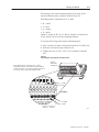
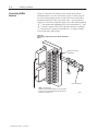
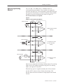
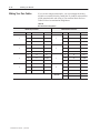
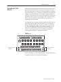
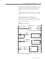
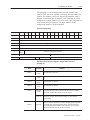
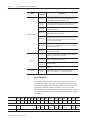
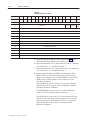
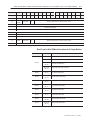
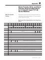
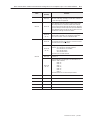
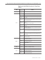
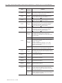
1
Allen-Bradley High Resolution Isolated Analog Modules (Cat. No. 1771-N Series) User Manual Important User Information Because of the variety of uses for the products described in this publication, those responsible for the application and use of this control equipment must satisfy themselves that all necessary steps have been taken to assure that each application and use meets all performance and safety requirements, including any applicable laws, regulations, codes and standards. The illustrations, charts, sample programs and layout examples shown in this guide are intended solely for example. Since there are many variables and requirements associated with any particular installation, Allen-Bradley does not assume responsibility or liability (to include intellectual property liability) for actual use based upon the examples shown in this publication. Allen-Bradley publication SGI–1.1, “Safety Guidelines For The Application, Installation and Maintenance of Solid State Control” (available from your local Allen-Bradley office) describes some important differences between solid-state equipment and electromechanical devices which should be taken into consideration when applying products such as those described in this publication. Reproduction of the contents of this copyrighted publication, in whole or in part, without written permission of Allen–Bradley Company, Inc. is prohibited. Throughout this manual we make notes to alert you to possible injury to people or damage to equipment under specific circumstances. ! ATTENTION: Identifies information about practices or circumstances that can lead to personal injury or death, property damage, or economic loss. Attention helps you: • identify a hazard • avoid the hazard • recognize the consequences Important: Identifies information that is especially important for successful application and understanding of the product. Important: We recommend you frequently backup your application programs on appropriate storage medium to avoid possible data loss. DeviceNet, DeviceNetManager, and RediSTATION are trademarks of Allen-Bradley Company, Inc. PLC, PLC–2, PLC–3, and PLC–5 are registered trademarks of Allen-Bradley Company, Inc. Windows is a trademark of Microsoft. Microsoft is a registered trademark of Microsoft IBM is a registered trademark of International Business Machines, Incorporated. All other brand and product names are trademarks or registered trademarks of their respective companies. Purpose of Manual This manual shows you how to use your high resolution isolated analog series input/output modules with an Allen-Bradley programmable controller. It helps you install, program, calibrate, and troubleshoot your modules. Audience You must be able to program and operate an Allen-Bradley programmable controller (PLC) to make efficient use of your analog module. In particular, you must know how to program block transfer instructions. We assume that you know how to do this in this manual. If you do not, refer to the appropriate PLC programming and operations manual before you attempt to program this module. Vocabulary In this manual, we refer to: • the individual module as the “module.” • the programmable controller, as the “controller” or the “processor.” Manual Organization This manual is divided into seven chapters. The following chart shows each chapter with its corresponding title and a brief overview of the topics covered in that chapter. Chapter Title Topics Covered 1 Overview of the High Resolution Isolated Analog Series Modules Descriptions of the modules, including general and hardware features 2 Installing the Module Module power requirements, keying, chassis location Wiring of module and remote termination panel 3 Communicating with your Analog Module How to program your programmable controller for this module Sample programs 4 Configuring the Module Hardware and software configuration Module write block format 5 Module Status and Input Data Reading data from your module Module read block format 6 Module Calibration How to calibrate your modules 7 Troubleshooting Diagnostics reported by the module Appendix A Specifications Your module’s specifications Appendix B Block Transfer Read and Write Configurations for 0 out/8 in Description of BTR/BTW words. Appendix C Block Transfer Read and Write Configurations for 8 out/0 in Description of BTR/BTW words. Publication 1771-6.5.127 – June 1999 P–2 Using this Manual Chapter Title Topics Covered Appendix D Block Transfer Read and Write Configurations for 2 out/2 in Description of BTR/BTW words. Appendix E Block Transfer Read and Write Configurations for 2 out/6 in Description of BTR/BTW words. Appendix F Block Transfer Read and Write Configurations for 1 out/7 in Description of BTR/BTW words. Appendix G Block Transfer Read and Write Configurations for 3 out/5 in Description of BTR/BTW words. Appendix H Block Transfer Read and Write Configurations for 4 out/4 in Description of BTR/BTW words. Appendix I Block Transfer Read and Write Configurations for 6 out/2 in Description of BTR/BTW words. Appendix J Block Transfer Read and Write Configurations for 5 out/3 in Description of BTR/BTW words. Appendix K Block Transfer Read and Write Configurations for 7 out/1 in Description of BTR/BTW words. Appendix L UL/CSA Hazardous Location Related Products You can install your module in any system that uses Allen-Bradley processors that support block transfer and the 1771 I/O structure. Contact your nearest Allen-Bradley office for more information about your programmable controllers. Product Compatibility These modules can only be used with 1771-A1B, A2B, A3B, A3B1, A4B or later 1771 I/O chassis and 1771-AM1, -AM2 chassis. Communication between the analog module and the processor is bidirectional. The processor block-transfers output data through the output image table to the module and block-transfers input data from the module through the input image table. The module also requires an area in the data table to store the read block and write block data. I/O image table use is an important factor in module placement and addressing selection. Refer to the table below. Compatibility and Use of Data Table Use of Data Table C t o Catalog Number 1771-N Series Compatibility Addressing Input Imagee Im Bits Output Image Im e Bits Read Block B ock Words Write Block B ock Words 1/2-slot 1-slot 2-slot 8 8 28 59 Yes Yes Yes Chassis Ch ssis A = Compatible with 1771-A1, A2, A4 chassis. B = Compatible with 1771-A1B, A2B, A3B, A3B1, A4B, 1771-AM1, -AM2 chassis. Yes = Compatible without restriction No = Restricted to complementary module placement Publication 1771-6.5.127 – June 1999 B Using this Manual P–3 You can place your analog module in any I/O module slot of the I/O chassis. Do not put the analog module in the same module group as a digital high density module unless you are using 1 or 1/2-slot addressing. Avoid placing the analog module close to ac modules or high voltage dc modules. Related Publications For a list of publications with information on Allen-Bradley programmable controller products, consult our publication index SD499. Publication 1771-6.5.127 – June 1999 Table of Contents Overview of the High Resolution Isolated Analog Modules Installing the Module Chapter 1 Chapter Objectives . . . . . . . . . . . . . . . . . . . . . . . . . . . . . . . . . . . Module Description . . . . . . . . . . . . . . . . . . . . . . . . . . . . . . . . . . . Features of the High Resolution Isolated Analog Series Modules . . . Catalog/Channel Numbers . . . . . . . . . . . . . . . . . . . . . . . . . . . . How the High Resolution Isolated Analog Modules Communicate with Processors . . . . . . . . . . . . . . . . . . . . . . . . . . . . . . . . . . . . . . Accuracy . . . . . . . . . . . . . . . . . . . . . . . . . . . . . . . . . . . . . . . . . . Chapter Summary . . . . . . . . . . . . . . . . . . . . . . . . . . . . . . . . . . . . 1–4 1–4 1–4 Chapter 2 Chapter Objectives . . . . . . . . . . . . . . . . . . . . . . . . . . . . . . . . . . . Before You Install Your Analog Module . . . . . . . . . . . . . . . . . . . . . European Union Directive Compliance . . . . . . . . . . . . . . . . . . . . . . EMC Directive . . . . . . . . . . . . . . . . . . . . . . . . . . . . . . . . . . . . . Low Voltage Directive . . . . . . . . . . . . . . . . . . . . . . . . . . . . . . . . Electrostatic Damage . . . . . . . . . . . . . . . . . . . . . . . . . . . . . . . . . . Calculating Power Requirements for the I/O Chassis . . . . . . . . . . . Determining Module Location in the I/O Chassis . . . . . . . . . . . . . . . Installing the Analog Module . . . . . . . . . . . . . . . . . . . . . . . . . . . . . Install the Module in the Chassis and Connect the Cable . . . . . . . . . Connecting Wiring . . . . . . . . . . . . . . . . . . . . . . . . . . . . . . . . . . . . Connecting 4-Wire Sensors . . . . . . . . . . . . . . . . . . . . . . . . . . . . . Sourcing Input Analog Modules . . . . . . . . . . . . . . . . . . . . . . . . . . . Making Your Own Cables . . . . . . . . . . . . . . . . . . . . . . . . . . . . . . . Grounding the Field Devices . . . . . . . . . . . . . . . . . . . . . . . . . . . . . Interpreting the Indicator Lights . . . . . . . . . . . . . . . . . . . . . . . . . . . Chapter Summary . . . . . . . . . . . . . . . . . . . . . . . . . . . . . . . . . . . . Communicating With Your Analog Module 1–1 1–1 1–2 1–3 2–1 2–1 2–1 2–1 2–2 2–2 2–2 2–3 2–3 2–4 2–6 2–10 2–11 2–12 2–13 2–14 2–14 Chapter 3 Chapter Objectives . . . . . . . . . . . . . . . . . . . . . . . . . . . . . . . . . . . Block Transfer Programming . . . . . . . . . . . . . . . . . . . . . . . . . . . . PLC-2 Programming . . . . . . . . . . . . . . . . . . . . . . . . . . . . . . . . . . PLC-3 Program Example . . . . . . . . . . . . . . . . . . . . . . . . . . . . . . . PLC-5 and PLC-5/250 Program Example . . . . . . . . . . . . . . . . . . . . Module Scan Time . . . . . . . . . . . . . . . . . . . . . . . . . . . . . . . . . . . . Programming Samples . . . . . . . . . . . . . . . . . . . . . . . . . . . . . . . . . Sample Ladder Diagram - PLC-3 Family Processors . . . . . . . . . . Sample Ladder Diagram - PLC-5 Family Processors . . . . . . . . . . Setting Up the Data Table File . . . . . . . . . . . . . . . . . . . . . . . . . . . . Chapter Summary . . . . . . . . . . . . . . . . . . . . . . . . . . . . . . . . . . . . 3–1 3–1 3–2 3–2 3–3 3–4 3–4 3–5 3–6 3–7 3–8 Publication 1771-6.5.127 – June 1999 toc–ii Table of Contents Configuring the Module Chapter 4 Chapter Objectives . . . . . . . . . . . . . . . . . . . . . . . . . . . . . . . . . . . Configuring the High Resolution Isolated Analog Modules . . . . . . . . Default Configurations . . . . . . . . . . . . . . . . . . . . . . . . . . . . . . . . . Module Level Programming Features . . . . . . . . . . . . . . . . . . . . . . Module “Configuration” Verification . . . . . . . . . . . . . . . . . . . . . . Temperature Scale . . . . . . . . . . . . . . . . . . . . . . . . . . . . . . . . . . Data Format . . . . . . . . . . . . . . . . . . . . . . . . . . . . . . . . . . . . . . Two’s Complement Binary . . . . . . . . . . . . . . . . . . . . . . . . . . Real Time Sampling . . . . . . . . . . . . . . . . . . . . . . . . . . . . . . . . . Output Channel Programming Features . . . . . . . . . . . . . . . . . . . . . Scaling . . . . . . . . . . . . . . . . . . . . . . . . . . . . . . . . . . . . . . . . . . Clamping . . . . . . . . . . . . . . . . . . . . . . . . . . . . . . . . . . . . . . . . Ramping . . . . . . . . . . . . . . . . . . . . . . . . . . . . . . . . . . . . . . . . . Alarm Enable . . . . . . . . . . . . . . . . . . . . . . . . . . . . . . . . . . . . . Reset State . . . . . . . . . . . . . . . . . . . . . . . . . . . . . . . . . . . . . . . Reset Value . . . . . . . . . . . . . . . . . . . . . . . . . . . . . . . . . . . . . . Input Channel Programming Features . . . . . . . . . . . . . . . . . . . . . . Scaling . . . . . . . . . . . . . . . . . . . . . . . . . . . . . . . . . . . . . . . . . . Alarms . . . . . . . . . . . . . . . . . . . . . . . . . . . . . . . . . . . . . . . . . . Alarm Deadband . . . . . . . . . . . . . . . . . . . . . . . . . . . . . . . . . . . Rate Alarm . . . . . . . . . . . . . . . . . . . . . . . . . . . . . . . . . . . . . . . Digital Filtering . . . . . . . . . . . . . . . . . . . . . . . . . . . . . . . . . . . . Thermocouple Type . . . . . . . . . . . . . . . . . . . . . . . . . . . . . . . . . RTD Type . . . . . . . . . . . . . . . . . . . . . . . . . . . . . . . . . . . . . . . . 10 Ohm Offset . . . . . . . . . . . . . . . . . . . . . . . . . . . . . . . . . . . . . Configuration Block for a Block Transfer Write . . . . . . . . . . . . . . . . Block Transfer Write Configuration Data Header . . . . . . . . . . . . . Module Configuration Data Header . . . . . . . . . . . . . . . . . . . . Bit/Word Description of Word 0 . . . . . . . . . . . . . . . . . . . . . . . Output Configuration Words 1 and 2 . . . . . . . . . . . . . . . . . . . Bit/Word Description of Output Configuration Words 1 and 2 . . Output Configuration Words 3 and 4 . . . . . . . . . . . . . . . . . . . Bit/Word Description of Output Configuration Words 3 and 4 . . Output Programming . . . . . . . . . . . . . . . . . . . . . . . . . . . . . . Output Configuration Words 5 through 10 . . . . . . . . . . . . . . . Bit/Word Description of Output Configuration Words 5 through 10 Input Programming . . . . . . . . . . . . . . . . . . . . . . . . . . . . . . . Bit/Word Description of Input Configuration Words 17 through 23 Chapter Summary . . . . . . . . . . . . . . . . . . . . . . . . . . . . . . . . . . . . Publication 1771-6.5.127 – June 1999 4–1 4–1 4–2 4–2 4–3 4–3 4–3 4–4 4–5 4–6 4–6 4–9 4–10 4–10 4–10 4–11 4–11 4–11 4–11 4–12 4–13 4–13 4–14 4–15 4–15 4–15 4–15 4–15 4–16 4–16 4–16 4–16 4–17 4–17 4–17 4–18 4–19 4–19 4–20 Table of Contents Module Status and Input Data Chapter 5 Module Calibration Chapter 6 Chapter Objectives . . . . . . . . . . . . . . . . . . . . . . . . . . . . . . . . . . . Reading Data from the Module . . . . . . . . . . . . . . . . . . . . . . . . . . . Block Transfer Read Data Format . . . . . . . . . . . . . . . . . . . . . . . . . “Outputs Only” Block Transfer Read Data Header . . . . . . . . . . . . “Inputs Only” and “Output/Input” Block Transfer Read Data Header Input Status Data . . . . . . . . . . . . . . . . . . . . . . . . . . . . . . . . . . . Bit/Word Description for Input Status Data Words . . . . . . . . . . Output Status Data . . . . . . . . . . . . . . . . . . . . . . . . . . . . . . . . . Bit/Word Description for Output Status Data Words . . . . . . . . . Chapter Summary . . . . . . . . . . . . . . . . . . . . . . . . . . . . . . . . . . . . Chapter Objective . . . . . . . . . . . . . . . . . . . . . . . . . . . . . . . . . . . . Tools and Equipment . . . . . . . . . . . . . . . . . . . . . . . . . . . . . . . . . . Calibrating Your Module . . . . . . . . . . . . . . . . . . . . . . . . . . . . . . . . Indicator Operation During Calibration . . . . . . . . . . . . . . . . . . . . Manual Calibration . . . . . . . . . . . . . . . . . . . . . . . . . . . . . . . . . . . . Input Channel Calibration . . . . . . . . . . . . . . . . . . . . . . . . . . . . . Output Channel Calibration . . . . . . . . . . . . . . . . . . . . . . . . . . . . Chapter Summary . . . . . . . . . . . . . . . . . . . . . . . . . . . . . . . . . . . . Troubleshooting 6–1 6–1 6–2 6–3 6–3 6–3 6–7 6–8 7–1 7–1 7–2 7–2 7–4 Appendix A Specifications . . . . . . . . . . . . . . . . . . . . . . . . . . . . . . . . . . . . . . . General Specifications . . . . . . . . . . . . . . . . . . . . . . . . . . . . . . . Block Transfer Write and Block Transfer Read Configurations for 0 Output/8 Input 1771-N Series Modules 5–1 5–1 5–2 5–2 5–3 5–4 5–5 5–6 5–7 5–7 Chapter 7 Chapter Objective . . . . . . . . . . . . . . . . . . . . . . . . . . . . . . . . . . . . Diagnostics Reported by the Module . . . . . . . . . . . . . . . . . . . . . . . Troubleshooting with the Indicators . . . . . . . . . . . . . . . . . . . . . . . . Status Reported by the Module . . . . . . . . . . . . . . . . . . . . . . . . . . . Chapter Summary . . . . . . . . . . . . . . . . . . . . . . . . . . . . . . . . . . . . Specifications toc–iii A–1 A–1 Appendix B What This Appendix Contains . . . . . . . . . . . . . . . . . . . . . . . . . . . . Block Transfer Write Configuration Block for 8 Input Modules . . . Block Transfer Write Bit/Word Descriptions for 8 Input Modules . . Block Transfer Read Word Assignments for 8 Input Modules . . . . Block Transfer Read Bit/Word Descriptions for 8 Input Modules . . B–1 B–1 B–3 B–5 B–7 Publication 1771-6.5.127 – June 1999 toc–iv Table of Contents Block Transfer Write and Block Transfer Read Configurations for 8 Output/0 Input 1771-N Series Modules Appendix C Block Transfer Write and Block Transfer Read Configurations for 2 Output/2 Input 1771-N Series Modules Appendix D Block Transfer Write and Block Transfer Read Configurations for 2 Output/6 Input 1771-N Series Modules Block Transfer Write and Block Transfer Read Configurations for 1 Output/7 Input 1771-N Series Modules Publication 1771-6.5.127 – June 1999 What This Appendix Contains . . . . . . . . . . . . . . . . . . . . . . . . . . . . Block Transfer Write Configuration Block for 8 Output Modules . . Block Transfer Write Bit/Word Descriptions for 8 Output Modules . Block Transfer Read Word Assignments for 8 Output Modules . . . Block Transfer Read Bit/Word Description for 8 Output Module . . C–1 C–1 C–3 C–5 C–6 What This Appendix Contains . . . . . . . . . . . . . . . . . . . . . . . . . . . . Block Transfer Write Configuration Block for the D–1 2 Output/2 Input Modules . . . . . . . . . . . . . . . . . . . . . . . . . . Block Transfer Write Bit/Word Descriptions for 2 Output/2 Input Modules . . . . . . . . . . . . . . . . . . . . . . . . . . Block Transfer Read Word Assignments for 2 Output/2 Input Module . . . . . . . . . . . . . . . . . . . . . . . . . . . Block Transfer Read Bit/Word Description for 2 Output/2 Input Module . . . . . . . . . . . . . . . . . . . . . . . . . . . D–1 D–2 D–5 D–6 Appendix E What This Appendix Contains . . . . . . . . . . . . . . . . . . . . . . . . . . . . Block Transfer Write Configuration Block for 2 Output/6 Input Modules . . . . . . . . . . . . . . . . . . . . . . . . . . Block Transfer Write Bit/Word Descriptions for 2 Output/6 Input Modules . . . . . . . . . . . . . . . . . . . . . . . . . . Block Transfer Read Word Assignments for 2 Output/6 Input Modules . . . . . . . . . . . . . . . . . . . . . . . . . . Block Transfer Read Bit/Word Description for 2 Output/6 Input Modules . . . . . . . . . . . . . . . . . . . . . . . . . . E–1 E–1 E–3 E–6 E–7 Appendix F What This Appendix Contains . . . . . . . . . . . . . . . . . . . . . . . . . . . . Block Transfer Write Configuration Block for 1 Output/7 Input Modules . . . . . . . . . . . . . . . . . . . . . . . . . . Block Transfer Write Bit/Word Descriptions for 1 Output/7 Input Modules . . . . . . . . . . . . . . . . . . . . . . . . . . Block Transfer Read Word Assignments for 1 Output/7 Input Module . . . . . . . . . . . . . . . . . . . . . . . . . . . Block Transfer Read Bit/Word Description for 1 Output/7 Input Module . . . . . . . . . . . . . . . . . . . . . . . . . . . F–1 F–1 F–3 F–6 F–7 Table of Contents Block Transfer Write and Block Transfer Read Configurations for 3 Output/5 Input 1771-N Series Modules Block Transfer Write and Block Transfer Read Configurations for 4 Output/4 Input 1771-N Series Modules Block Transfer Write and Block Transfer Read Configurations for 6 Output/2 Input 1771-N Series Modules Block Transfer Write and Block Transfer Read Configurations for 5 Output/3 Input 1771-N Series Modules toc–v Appendix G What This Appendix Contains . . . . . . . . . . . . . . . . . . . . . . . . . . . . Block Transfer Write Configuration Block for 3 Output/5 Input Modules . . . . . . . . . . . . . . . . . . . . . . . . . . Block Transfer Write Bit/Word Descriptions for 3 Output/5 Input Modules . . . . . . . . . . . . . . . . . . . . . . . . . . Block Transfer Read Word Assignments for 3 Output/5 Input Modules . . . . . . . . . . . . . . . . . . . . . . . . . . Block Transfer Read Bit/Word Descriptions for 3 Output/5 Input Modules . . . . . . . . . . . . . . . . . . . . . . . . . . G–1 G–1 G–3 G–6 G–7 Appendix H What This Appendix Contains . . . . . . . . . . . . . . . . . . . . . . . . . . . . Block Transfer Write Configuration Block for 4 Output/4 Input Modules . . . . . . . . . . . . . . . . . . . . . . . . . . Block Transfer Write Bit/Word Descriptions for 4 Output/4 Input Modules . . . . . . . . . . . . . . . . . . . . . . . . . . . Block Transfer Read Word Assignments for 4 Output/4 Input Modules . . . . . . . . . . . . . . . . . . . . . . . . . . Block Transfer Read Bit/Word Descriptions for 4 Output/4 Input Modules . . . . . . . . . . . . . . . . . . . . . . . . . . . H–1 H–1 H–3 H–6 H–7 Appendix I What This Appendix Contains . . . . . . . . . . . . . . . . . . . . . . . . . . . . Block Transfer Write Configuration Block for 6 Output/2 Input Modules . . . . . . . . . . . . . . . . . . . . . . . . . . Block Transfer Write Bit/Word Descriptions for 6 Output/2 Input Modules . . . . . . . . . . . . . . . . . . . . . . . . . . Block Transfer Read Word Assignments for 6 Output/2 Input Modules . . . . . . . . . . . . . . . . . . . . . . . . . . Block Transfer Read Bit/Word Descriptions for 6 Output/2 Input Modules . . . . . . . . . . . . . . . . . . . . . . . . . . I–1 I–1 I–3 I–6 I–8 Appendix J What This Appendix Contains . . . . . . . . . . . . . . . . . . . . . . . . . . . . Block Transfer Write Configuration Block for 5 Output/3 Input Modules . . . . . . . . . . . . . . . . . . . . . . . . . . Block Transfer Write Bit/Word Descriptions for 5 Output/3 Input Modules . . . . . . . . . . . . . . . . . . . . . . . . . . Block Transfer Read Word Assignments for the 5 Output/3 Input Modules . . . . . . . . . . . . . . . . . . . . . . . . . . Block Transfer Read Bit/Word Descriptions for 5 Output/3 Input Modules . . . . . . . . . . . . . . . . . . . . . . . . . . J–1 J–1 J–3 J–6 J–7 Publication 1771-6.5.127 – June 1999 toc–vi Table of Contents Block Transfer Write and Block Transfer Read Configurations for 7 Output/1 Input 1771-N Series Modules CSA Hazardous Location Appendix K What This Appendix Contains . . . . . . . . . . . . . . . . . . . . . . . . . . . . Block Transfer Write Configuration Block for 7 Output/1 Input Modules . . . . . . . . . . . . . . . . . . . . . . . . . . Block Transfer Write Bit/Word Descriptions for 7 Output/1 Input Modules . . . . . . . . . . . . . . . . . . . . . . . . . . Block Transfer Read Word Assignments for 7 Output/1 Input Modules . . . . . . . . . . . . . . . . . . . . . . . . . . Block Transfer Read Bit/Word Descriptions for 7 Output/1 Input Modules . . . . . . . . . . . . . . . . . . . . . . . . . . K–1 K–3 K–6 K–7 Appendix L CSA Hazardous Location . . . . . . . . . . . . . . . . . . . . . . . . . . . . . . . Publication 1771-6.5.127 – June 1999 K–1 L–1 Chapter 1 Overview of the High Resolution Isolated Analog Modules Chapter Objectives This chapter gives you information on: • features of the input/output modules • how the modules communicate with programmable controllers Module Description The high resolution isolated analog modules are intelligent block transfer modules that interface analog signals with Allen-Bradley PLC-3 and PLC-5 family programmable controllers that have block transfer capability. Block transfer programming moves input data words from the module’s memory to a designated area in the processor data table in a single scan. It also moves configuration words and output data from the processor data table to module memory. The N-series family includes modules with both analog inputs and outputs on the same module. The modules use 16-bit analog-to-digital converters and 14-bit digital-to-analog converters for high resolution and accuracy. All of these modules require only a single slot in the I/O chassis, and do not require an external power supply. Since the N-series modules are combination modules, with input and output capabilities on the same module, block transfer reads from the module are structured differently from dedicated input or output modules. Normally, block transfer read information is contiguous, and is stored in contiguous locations in the data block. N-series modules transmit channel data on an individual basis with status information in between. This results in non-contiguous blocks of data in non-contiguous data locations. Care must be taken when transferring this information. Additional programming may be required. Important: Use with PLC-2 family programmable controllers is not recommended. Refer to chapter 3, page 3-2. Input data is converted to a specified data type in a digital format to be transferred to the processor’s data table on request. Output data is converted to analog signals and sent to the appropriate output channels. If real time sampling is selected, block transfer reads will only occur at the time selected. Consequently, the minimum interval between block transfer reads is the same as the total input update time for each analog input module (25ms). Publication 1771-6.5.127 – June 1999 1–2 Overview of the High Resolution Isolated Analog Modules The modules have either four or eight channels, each electrically isolated from each other and from the backplane. Input and output terminations are made through prefabricated cables which connect to remote termination panels (RTP). The modules are compatible with all 1771-A1B, A2B, A3B, A3B1, A4B, and later 1771 universal I/O chassis. In addition, they can be used in 1771-AM1, and -AM2 chassis. Features of the High Resolution Isolated Analog Series Modules The analog modules are comprised of modular analog signal conditioning blocks that are plugged into a common circuit board. These signal conditioning blocks provide the following: • • • • • • • • 4–20mA output range 0–50mA output range +10V output (scalable +5V, 0-5V, 0-10V, etc.) thermocouple input (+100mV) +5V input (+20mA with resistor RTP) +10V input (+20mA with resistor RTP) 4–20mA input with sourcing/sinking input 1–650 ohm RTD input Your particular module may have a combination of the above conditioning blocks. The N-Series analog modules feature: • • • • • • • scaling of data to engineering units self-calibration (external reference required) software configuration user-selectable high and low alarms with deadband (hysteresis) self diagnostics input open circuit detection programmable ramped outputs Specific analog modules have these additional features: • Thermocouple input channels – input channels configurable for thermocouple input ranges — – – – – Publication 1771-6.5.127 – June 1999 Types B, E, J, K, R, S and T thermocouples (1771-NT2 also includes types C and N) cold junction compensation scaling to selected temperature range in oC or oF temperature resolution — up to 0.03oC/0.06°F (E, J, K, T, N) up to 0.1oC/0.2°F (B, R, S) up to 0.07oC/0.1°F (C) millivolt resolution up to 1 microvolt Overview of the High Resolution Isolated Analog Modules 1–3 • RTD input channels – reports oC, oF, or ohms for 100Ω platinum, 120Ω nickel, or • • • • • 10Ω copper sensors – reports ohms for other types of sensors – 0.1oC/0.1oF resolution on 100Ω platinum sensor – resistance resolution to 10mΩ +5V and +10V input channels — can be used with remote termination panel resistor to achieve a nonsourcing current input 4-20mA input with internal loop power supply ±10V output channels 0-25mA output channels 0-50mA output channels Catalog/Channel Numbers The following are standard catalog numbers and their respective channel configurations: Module Channel 1 Channel 2 Channel 3 Channel 4 Channel 5 Channel 6 Channel 7 Channel 8 Refer to Appendix 1771-NIS 4–20mA 4–20mA 4–20mA 4–20mA 4–20mA 4–20mA 4–20mA 4–20mA B 1771-NIV +5V (+20mA) +5V (+20mA) +5V (+20mA) +5V (+20mA) +5V (+20mA) +5V (+20mA) +5V (+20mA) +5V (+20mA) B 1771-NIV1 +10V +10V +10V +10V +10V +10V +10V +10V B 1771-NIVR +5V (+20mA) +5V (+20mA) +5V (+20mA) +5V (+20mA) RTD RTD RTD RTD B 1771-NIVT +5V (+20mA) +5V (+20mA) +5V (+20mA) +5V (+20mA) +100mV/TC +100mV/TC +100mV/TC +100mV/TC B 1771-NR RTD RTD RTD RTD RTD RTD RTD RTD B 1771-NT1 +100mV/TC +100mV/TC +100mV/TC +100mV/TC +100mV/TC +100mV/TC +100mV/TC +100mV/TC B 1771-NT2 –5/+55mV/TC –5/+55mV/TC –5/+55mV/TC –5/+55mV/TC –5/+55mV/TC –5/+55mV/TC –5/+55mV/TC –5/+55mV/TC B 1771-NOC 0–25mA out 0–25mA out 0–25mA out 0–25mA out 0–25mA out 0–25mA out 0–25mA out 0–25mA out C 1771-NOV +10V out +10V out +10V out +10V out +10V out +10V out +10V out +10V out C 1771-NB4T 0–25mA out 0–25mA out +100mV/TC +100mV/TC D 1771-NB4S 0–25mA out 0–25mA out 4–20mA 4–20mA D 1771-NBSC 0–25mA out 0–25mA out 4–20mA 4–20mA 4–20mA 4–20mA 4–20mA 4–20mA E 1771-NBRC 0–25mA out 0–25mA out RTD RTD RTD RTD RTD RTD E 1771-NBTC 0–25mA out 0–25mA out +100mV/TC +100mV/TC +100mV/TC +100mV/TC +100mV/TC +100mV/TC E 1771-NBV1 +10V out +10V out +10V in +10V in +10V in +10V in +10V in +10V in E 1771-NBVC 0–25mA out 0–25mA out +5V (+20mA) +5V (+20mA) +5V (+20mA) +5V (+20mA) +5V (+20mA) +5V (+20mA) E 1771-NX1 0–50mA out 0–25mA out 0–50mA out 0–25mA out 0–25mA out RTD RTD 100mV/TC F 1771-NX2 0–50mA out 0–25mA out 0–50mA out 0–25mA out RTD RTD 100mV/TC 100mV/TC G 1771-NX3 0–50mA out 0–25mA out 0–50mA out 0–25mA out RTD RTD RTD 100mV/TC G 1771-NX4 0–50mA out 0–25mA out 0–25mA out 0–25mA out 0–25mA out 0–25mA out RTD 100mV/TC H Note: Appendices I thru L cover other variations of the 1771-N series module. Publication 1771-6.5.127 – June 1999 1–4 Overview of the High Resolution Isolated Analog Modules How the High Resolution Isolated Analog Modules Communicate with Processors The processor transfers data to and from the module using BTW (block transfer write) and BTR (block transfer read) instructions in your ladder diagram program. These instructions let the processor obtain input values and status from the module, and let you establish the module’s mode of operation (Figure 1.A). 1. The processor transfers your configuration data, output data and calibration values to the module using a block transfer write instruction. 2. External input devices generate analog signals that are transmitted to the module. Internal output circuitry generates analog signals that drive field devices. 3. The module converts the analog signals into binary or BCD format and stores theses values until the processor requests their transfer. Table 1.A Communication Between the Processor and the Module 3 5 Memory User Program 1 BTW From input devices To output devices 2 BTR 4 High Resolution PLC Processor (PLC-5/40 Shown) Isolated Analog Module 12933-I 4. When instructed by your ladder program, the processor performs a read block transfer of the values and stores them in a data table. 5. The processor and module determine that the transfer was made without error, and that input values are within specified range. 6. Your ladder program can use and/or move the data (if valid) before it is written over by the transfer of new data in a subsequent transfer. See chapter 4, “Configuring the Module,” for more information. Accuracy The accuracy of each of the high resolution isolated analog modules is described in Appendix A. Chapter Summary In this chapter you read about the functional aspects of the analog modules and how they communicate with programmable controllers. Publication 1771-6.5.127 – June 1999 Chapter 2 Chapter Objectives Before You Install Your Analog Module This chapter gives you information on: For information on See page Before You Install Your Module . . . . . . . . . . . . . . . . . . . . . . . European Union Directives . . . . . . . . . . . . . . . . . . . . . . . . . . Determining Power Requirements . . . . . . . . . . . . . . . . . . . . Determining Module Location in the Chassis . . . . . . . . . . . . . Installing the Module . . . . . . . . . . . . . . . . . . . . . . . . . . . . . . Connecting Wiring . . . . . . . . . . . . . . . . . . . . . . . . . . . . . . . . Connecting 4–wire sensors . . . . . . . . . . . . . . . . . . . . . . . . . Sourcing input Analog Modules . . . . . . . . . . . . . . . . . . . . . . Making Your Own Cables . . . . . . . . . . . . . . . . . . . . . . . . . . . Grounding Field Devices . . . . . . . . . . . . . . . . . . . . . . . . . . . Module Indicators . . . . . . . . . . . . . . . . . . 2–1 2–1 2–2 2–3 2–3 2–6 2–10 2–11 2–12 2–13 2–14 Before installing your module in the I/O chassis you must: Action required: European Union Directive Compliance Refer to: Calculate power requirements for the I/O chassis. page 2–2 Determine module location in the I/O Chassis page 2–3 Connect the cable and make wiring connections to the remote termination panel page 2–4 If this product has the CE mark it is approved for installation within the European Union and EEA regions. It has been designed and tested to meet the following directives. EMC Directive This product is tested to meet Council Directive 89/336/EEC Electromagnetic Compatibility (EMC) and the following standards, in whole or in part, documented in a technical construction file: • EN 50081-2EMC – Generic Emission Standard, Part 2 – Industrial Environment • EN 50082-2EMC – Generic Immunity Standard, Part 2 – Industrial Environment This product is intended for use in an industrial environment. Publication 1771-6.5.127 – June 1999 2–2 Installing the Module Low Voltage Directive This product is tested to meet Council Directive 73/23/EEC Low Voltage, by applying the safety requirements of EN 61131–2 Programmable Controllers, Part 2 – Equipment Requirements and Tests. For specific information required by EN 61131-2, see the appropriate sections in this publication, as well as the following Allen-Bradley publications: • Industrial Automation Wiring and Grounding Guidelines For Noise Immunity, publication 1770-4.1 • Guidelines for Handling Lithium Batteries, publication AG-5.4 • Automation Systems Catalog, publication B111 This equipment is classified as open equipment and must be mounted in an enclosure during operation to provide safety protection. Electrostatic Damage Electrostatic discharge can damage semiconductor devices inside this module if you touch backplane connector pins. Guard against electrostatic damage by observing the following warning: ! ATTENTION: Electrostatic discharge can degrade performance or cause permanent damage. Handle the module as stated below. • Wear an approved wrist strap grounding device when handling the module. • Touch a grounded object to rid yourself of electrostatic charge before handling the module. • Handle the module from the front, away from the backplane connector. Do not touch backplane connector pins. • Keep the module in its static-shield bag when not in use, or during shipment. Calculating Power Requirements for the I/O Chassis Your module receives its power through the 1771 I/O chassis backplane from the chassis power supply. The maximum current drawn by the module from this supply ranges from 1.5 to 3.3A, dependent upon the particular type of module. Refer to the specifications in appendix A for standard modules. Add this value to the requirements of all other modules in the I/O chassis to prevent overloading the chassis backplane and/or backplane power supply. Publication 1771-6.5.127 – June 1999 Installing the Module Determining Module Location in the I/O Chassis 2–3 Place your module in any slot of the I/O chassis except for the extreme left slot. This slot is reserved for processors or adapter modules. Group your modules to minimize adverse affects from radiated electrical noise and heat. We recommend the following. • Group analog and low voltage dc modules away from ac modules or high voltage dc modules to minimize electrical noise interference. • Do not place this module in the same I/O group with a discrete high-density I/O module when using 2-slot addressing. This module uses a byte in both the input and output image tables for block transfer. Installing the Analog Module To install your module in an I/O chassis: 1. First, turn off power to the I/O chassis: ! ATTENTION: Remove power from the 1771 I/O chassis backplane and disconnect the cable from the module before removing or installing an I/O module. • Failure to remove power from the backplane could cause injury or equipment damage due to possible unexpected operation. • Failure to remove power from the backplane could cause module damage, degradation of performance, or injury. ! ATTENTION: Observe the following precautions when inserting or removing keys: • insert or remove keys with your fingers • make sure that key placement is correct Incorrect keying or the use of a tool can result in damage to the backplane connector and possible system faults. Publication 1771-6.5.127 – June 1999 2–4 1 Installing the Module Key the Backplane Connector Place your module in any slot in the chassis except the leftmost slot which is reserved for processors or adapters. Position the keying bands in the backplane connectors to correspond to the key slots on the module. I/O chassis Place the keying bands: between 26 and 28 between 32 and 34 Keying Bands You can change the position of these bands if subsequent system design and rewiring makes insertion of a different type of module necessary. Upper Connector 11022-I Install the Module in the Chassis and Connect the Cable ! ATTENTION: Remove power from the 1771 I/O chassis backplane and field wiring arm before removing or installing an I/O module. • Failure to remove power from the backplane or wiring arm could cause module damage, degradation of performance, or injury. • Failure to remove power from the backplane could cause injury or equipment damage due to possible unexpected operation. 1. Place the module in the plastic tracks on the top and bottom of the slot that guides the module into position. 2. Do not force the module into its backplane connector. Apply firm even pressure on the module until it is firmly seated in the chassis. Note: The chassis locking bar will not close if all modules are not seated properly. Publication 1771-6.5.127 – June 1999 Installing the Module 1 1771-A1B, -A2B, -A3B, -A3B1, -A4B I/O chassis locking tab 2–5 1771-A1B, -A2B, -A3B1, -A4B Series B I/O chassis locking bar pin locking bar card guides card guides module Snap the chassis latch over the top of the module to secure it. module Swing the chassis locking bar down into place to secure the modules. Make sure the locking pins engage. 19809 3. Connect the 1771-NC cable to the module as shown in 2.1. A. Slide the locking bar up. B. Insert the cable connector into the mating connector on the front of the module. C. Slide the locking bar down over the mating pins on the module to lock the connector onto the module. Figure 2.1 Connecting the Cable to the Front of the Module 1. Position locking bar in up position. 2. Insert connector into mating connector. 3. Slide locking bar down to lock. Cable Connector Module Connector Locking bar 11023-I Publication 1771-6.5.127 – June 1999 2–6 Installing the Module Connecting Wiring The N-series modules are cable-connected to a remote termination panel using cat. no. 1771-NC6 (6 ft) or -NC15 (15 ft) cables. Variations of remote termination panels are used, depending on the type of module used. These are: Catalog Number Description 1771-RTP1 has cold junction compensation for thermocouples 1771-RTP3 incorporates resistors and fuses; used primarily for 4-20mA inputs when using +5V inputs (Uses 5mm x 20mm fast acting 1/4A fuses such as Bussmann GMA–1/4, 250V/250mA.) 1771-RTP4 a general-use block with straight-thru wiring that can be used for all applications except thermocouples1 1771-RT41 a 4-channel block with cold junction compensation for thermocouples 1771-RT44 a general-use 4-channel block with straight-thru wiring that can be used for all applications except thermocouples1 1 RTP4 and RT44 can be used with thermocouples if a method of cold junction compensation is provided at the interface of thermocouple and copper wires within the system. The remote termination panels are designed for mounting on standard DIN 1 or DIN 3 mounting rails. Figure 2.2 Mounting Dimensions for the Remote Termination Panels RTP1, RTP3, RTP4 B A Inches (Millimeters) 3.0 (75.0 ) J8 J7 J6 J5 J1 J2 J3 J4 2.3 (58.4 ) 5.30 (134.6 ) Dimensions back of DIN rail RT41, RT44 3.0 (75.0 ) J1 J2 J3 J4 2.3 (58.4 ) Publication 1771-6.5.127 – June 1999 3.5 (88.9 ) 2.3 (58.4) 19 Installing the Module 2–7 Table 2.A Remote Termination Panel Connection Points for Field Devices (Channel 1 shown) Input Type Voltage Output Type Voltage Connect To + I1 - R1 Shield S1 Connect To + O1 - R1 Shield S1 Input Type Connect Current (with it external re i tor resistor) Output Type Current To + I1 - R1 Shield S1 Connect To + O1 - R1 Shield S1 Input Type Thermocouple Input Type RTD1 Connect To + I1 - R1 Shield S1 Connect To Excitation (A) O1 Lead Compensation (B) I1 Common (C) R1 Input Type Current (Source/ Source Sink) Connect To + I1 -2 R1 Shield S1 Loop Power O1 1 When using 4-wire RTD, leave the 4th wire open. 2 Not used when N-Series module is supplying loop power. Refer to Figure 2.6 in this document. Publication 1771-6.5.127 – June 1999 2–8 Installing the Module Figure 2.3 Remote Termination Panel Wiring Example: Module End of 1771-NC cable Channel 1 Connections R1 = Return 1 I1 = Input 1 O1 = Output 1 S1 = Shield 1 Note: Terminals W1, W2 and W3 are spares. Do not use terminals CR and CL. RTP1 RTP End of 1771-NC cable DIN Rail Channel 1 Connections R1 = Return 1 I1 = Input 1 O1 = Output 1 S1 = Shield 1 Module End of 1771-NC cable Note: Terminals W1, W2 and W3 are spares. Do not use terminals CR and CL. RT41 RTP End of 1771-NC cable DIN Rail 11024-I Publication 1771-6.5.127 – June 1999 Installing the Module 2–9 Field wiring to the remote termination panel is the same for all remote termination panel variations. Refer to Figure 2.4. Each channel has 4 connections: R, I, O, and S. • • • • R = return I = input O = output S = shield Channel 1 would use R1, I1, O1, and S1; channel 2 would use R2, I2, O2, and S2; and so on for the remaining channels. To connect field wiring to the remote termination panel: 1. Strip 3/8 inch (9.25 mm) of insulation from the 22-12 AWG wire. 2. Insert the wire into the open connector slot. 3. Tighten the screw to 4.4–5.2 lb–in. (0.5–0.6Nm) to clamp the wire. Figure 2.4 Connecting Wire to the Remote Termination Panel Each channel has four connections: R, I, O, and S. Field wiring to the RTP is the same for all RTP variations. Channel 1 uses R1, I1, O1, and S1; channel 2 uses R2, I2, O2, and S2; and so on for the remaining channels. Remote Termination Panel (RTP) I = input R = return Field Wiring O = output S = shield channel 2 channel 1 19621 Publication 1771-6.5.127 – June 1999 2–10 Installing the Module Connecting 4-Wire Sensors Figure 2.5 shows how to connect 4-wire sensors to the remote termination panel. A 4-wire sensor has two pairs of leads; one pair for each resistor junction. One wire of the four is not used (it does not matter which one). This leaves three wires – one pair and one single wire. You must connect the single wire to the terminal marked “O_”. You connect the remaining pair of wires to terminals “I_” and “R_”. It doesn’t matter which wire of the pair connects to terminal “I_” and which wire connects to terminal “R_” so long as all three wires are the same AWG gauge. Figure 2.5 Connecting a 4-Wire Sensor to the Remote Termination Panel Single lead connects to terminal O Chassis Ground RTD Leave 1 lead open Note: In this illustration: Terminal O is the 1mA excitation (A) sourcing current Terminal I is the lead compensation (B) sense input Terminal R is common (C) Publication 1771-6.5.127 – June 1999 12935–I Installing the Module Sourcing Input Analog Modules 2–11 The 1771-NIS, 1771-NBSC and 1771-NB4S modules are sourcing/sinking input modules. These modules can supply the necessary loop power for 2-wire transmitters connected to the input. All loop power functionality is contained within the analog module. Examples of typical configurations are shown in Figure 2.6. No external resistors are required. Figure 2.6 Examples of Sourcing/Sinking Input Modules RTP4 2-Wire Transmitter i 24V dc Output Input Input Module supplies loop power (sourcing) Return 24V dc Output 4-Wire Transmitter i 24V dc Input Input User supplies loop power with 4-wire transmitter (sinking) Return 24V dc Output 2-Wire Transmitter 24V dc i Input Input User supplies loop power (sinking) Return Inputs can be configured as sourcing or sinking inputs. For sourcing inputs, the N-series module supplies the loop power. For sinking inputs, you supply the loop power. When the loop power is supplied externally, the 16-bit resolution provides 65535 counts over the 0–20mA current range. This provides about twice the resolution of voltage inputs with external resistors. Publication 1771-6.5.127 – June 1999 2–12 Installing the Module Making Your Own Cables If you are not using thermocouples, you can terminate the analog module to a terminal block by cutting the 25-pin RTP end connector off the standard cable and wiring to your terminal block. Refer to Table 2.B for wire termination designations. Table 2.B Wire Termination Designations Module Top Connector Channel Number 1 2 3 4 Module Bottom Connector Signal 37-Pin Connector Wire Color I1 20 Blk O1 22 Blk/Wht R1 21 I2 Channel Number Signal 37-Pin Connector Wire Color I5 20 Blk O5 22 Blk/Wht Wht/Blk R5 21 Wht/Blk 24 Orn I6 24 Orn O2 26 Orn/Blk O6 26 Orn/Blk R2 25 Wht R6 25 Wht I3 29 Grn I7 29 Grn O3 31 Grn/Blk O7 31 Grn/Blk R3 30 Grn/Wht R7 30 Grn/Wht I4 33 Blu I8 33 Blu O4 35 Blu/Blk O8 35 Blu/Blk R4 34 Blu/Wht R8 34 Blu/Wht 36 Red 37 Red/Wht 5 6 7 8 Cold Junction Thermistor er i tor Publication 1771-6.5.127 – June 1999 Installing the Module Grounding the Field Devices 2–13 When using shielded cable or shielded thermocouple extension wire, ground the foil shield and drain wire only at one end of the cable. We recommend that you wrap the foil shield and drain wire together and connect them to the “S” connection on the RTP for the particular channel. All shield connections are internally connected together in the RTP so that only one wire is required to ground the entire remote termination panel. Connect a wire from the “SH” connection on the RTP to a ground stud on the metal cabinet in which the remote termination panel is mounted. If you do not want to ground a particular shield at the RTP, you can remove the jumper for that particular channel. This will allow the shield to float at the RTP end. To remove a jumper, you must cut it out. Once the jumper is removed it cannot be replaced. Clip as close to the circuit board as possible at both ends to completely remove it. The jumpers (Figure 2.7) are labeled J1 through J8, corresponding to channels 1 through 8 respectively. Figure 2.7 Jumper Positions Jumpers for channels 5 through 8 J8 J1 J7 J6 J5 J2 J3 J4 Jumpers for channels 1 through 4 Refer to publication 1770-4.1, Programmable Controller Wiring and Grounding Guidelines, for additional information. Publication 1771-6.5.127 – June 1999 2–14 Installing the Module Interpreting the Indicator Lights The front panel of the analog module contains two bi-color indicators: a red/green RUN/FLT (fault) indicator and a red/green CAL/COM indicator (Figure 2.8). Figure 2.8 Diagnostic Indicators RUN/FLT CAL/COM Run/Fault indicator. This indicator will flash green until the first valid block transfer write has been received. If a fault is found initially or occurs later, the RUN/FLT indicator turns red. Calibrate/communication indicator. This indicator will flash green when doing block transfers. It will flash red during calibration. 10528-I At power-up, an initial module self-check occurs. The RUN/FLT indicator will be green when the check is completed satisfactorily. It will flash green until the first valid block transfer write has been received. If a fault is found initially or occurs later, the RUN/FLT indicator turns red. The bottom indicator is the calibrate/communication indicator. This indicator will flash green when doing block transfers. It will flash red during calibration. Possible module fault causes and corrective action are discussed in Chapter 7, “Troubleshooting.” Chapter Summary Publication 1771-6.5.127 – June 1999 In this chapter you learned how to install your module in an existing programmable controller system and how to wire to the remote termination panel. Chapter 3 Communicating With Your Analog Module Chapter Objectives In this chapter, we describe • block transfer programming • quick-startup sample programs for the PLC-3 and PLC-5 processors • module scan time issues Block Transfer Programming Your module communicates with the processor through bidirectional block transfers. This is the sequential operation of both read and write block transfer instructions. For the 1771-N series modules, block transfer writes (BTWs) can perform two different functions. If you want to: Description This type of BTW is called: configure the module This involves setting the bits which enable the programmable features of the module, such as scaling, alarming, real time sampling, etc. the “configuration BTW” send data to the output channels of those modules having outputs This type of BTW is generally shorter in length than the configuring BTW because it does not configure the module each time it is initiated. the “output update BTW” A configuration BTW is initiated when the analog module is first powered up, and subsequently only when the programmer wants to enable or disable features of the module. An output update BTW is initiated when the programmer wants the output channels on the module to change value. This shortened version of the BTW allows faster response time from the output channels. The following example programs are minimum programs; all rungs and conditioning must be included in your application program. You can disable BTRs, or add interlocks to prevent writes if desired. Do not eliminate any storage bits or interlocks included in the sample programs. If interlocks are removed, the program may not work properly. Publication 1771-6.5.127 – June 1999 3–2 Communicating With Your Analog Module Your analog module works with a default configuration upon powerup as long as a block transfer write (BTW) has not been initiated. See the configuration default section in chapter 4 to understand what this configuration looks like. Refer to the sample programs in this chapter to get started. Your program should monitor status bits (such as overrange, underrange, alarms, etc.) and block transfer read activity. The following example programs illustrate the minimum programming required for the 1771-N series module to powerup and operate. PLC-2 Programming Due to the number of digits required for high resolution readings, the 1771-N series modules normally read input values in 2’s complement binary. Binary coded decimal (BCD) can be used, but with lower resolution. As a result, the 1771-N series modules are not recommended for use with PLC-2 family programmable controllers. PLC-3 Program Example Block transfer instructions with the PLC-3 processor use three data table files. A binary file is used for module location and other related data. This is the block transfer control file. Two separate block transfer data files store data that you want transferred to the module (when programming a block transfer write) or from the module (when programming a block transfer read). The address of the block transfer data files are stored in the block transfer control file. The industrial terminal prompts you to create a control file when a block transfer instruction is being programmed. The same block transfer control file is used for both the read and write instructions for your module. A different block transfer control file is required for every module. An example program segment with block transfer instructions is shown in Figure 3.1, and described below. Publication 1771-6.5.127 – June 1999 Communicating With Your Analog Module 3–3 Figure 3.1 PLC-3 Family Sample Program Structure Program Action At powerup, the user program enables a block transfer read. Then it initiates a block transfer write to configure module. Thereafter, the program continuously performs read and write block transfers. PLC-5 and PLC-5/250 Program Example 1 2 Block Transfer Read Done Bit Block Transfer Write Done Bit BTR BLOCK XFER READ RACK: XXX GROUP: X MODULE: X = XXXX DATA: XXXX:XXXX LENGTH: 00 CNTL: XXXX:XXXX BTW BLOCK XFER WRITE RACK: XXX GROUP: X MODULE: X = XXXX DATA: XXXX:XXXX LENGTH: 00 CNTL: XXXX:XXXX Enable EN 12 Done DN 15 Error ER 13 Enable EN 02 Done DN 05 Error ER 03 This program is very similar to the PLC-3 program with the following exceptions: • Block transfer enable bits are used instead of done bits as the conditions on each rung. • Separate block transfer control files are used for the block transfer instructions. Figure 3.2 PLC-5 Family Sample Program Structure Program Action At powerup, the user program enables a block transfer read. Then it initiates a block transfer write to configure module. BTR Enable 1 BTR Enable Thereafter, the program continuously performs read and write block transfers. BTW Enable 2 BTW Enabl e BTR BLOCK XFER READ X RACK: X GROUP: X MODULE: XXX:XX CONTROL: XXX:XX DATA FILE: 00 LENGTH: N CONTINUOUS: BTW BLOCK XFER WRITE X RACK: X GROUP: X MODULE: XXX:XX CONTROL: XXX:XX DATA FILE: 00 LENGTH: CONTINUOUS: N EN DN ER EN DN ER Publication 1771-6.5.127 – June 1999 3–4 Communicating With Your Analog Module Module Scan Time Scan time is defined as the amount of time it takes for the module to read the input channels and place new data into the data buffer and/or read the data buffer and write new data to the output channels. Scan time for your module is shown in Figure 3.3. Figure 3.3 Block Transfer Time Module available to perform block transfer End of Block Transfer Write Block Transfer Write Time 1 Configure Time 2 1st Scan 3 2nd Scan 4 5 3rd Scan 6 Internal scan time = 25ms 10529-I The following description references the sequence numbers in Figure 3.3. Following a block transfer write (1) the module inhibits communication until after it has configured the data and loaded calibration constants (2), scanned the inputs and/or outputs (3), and filled the data buffer (4). Configuration block transfers, therefore, should only be performed when the module is being configured or calibrated. Any time after the buffer is filled (4), a block transfer read (BTR) request can be acknowledged. When operated in the default mode, new data will be available for a BTR every 25 milliseconds. When operated in real time sample mode (RTS = T), BTRs will be ignored by the module for “T” milliseconds, at which time a single BTR will be allowed. Programming Samples The following are sample programs for using your modules more efficiently when operating with the PLC-3 or PLC-5 family processors. These programs show you how to configure the module and read data from the module, and efficiently update the output channels on those modules with outputs. Refer to the proper PLC-3 or PLC-5 documentation for additional information on processor programming and data entry. Publication 1771-6.5.127 – June 1999 Communicating With Your Analog Module 3–5 The differences between the types of 1771-N series modules is related to the number of output channels each module has. A module with only inputs (no outputs) requires one BTW after powerup. Thereafter, it sends back input data and module status by way of BTRs. A module with outputs requires BTWs to configure it and update its output data. BTRs are required to send back input data and module status. Sample Ladder Diagram - PLC-3 Family Processors The following PLC-3 program can be used for all 1771-N series modules. The program can be altered to effectively address modules with or without output channels. Figure 3.4 PLC-3 Family Example Program Structure BTR BLOCK XFER READ RACK: GROUP: MODULE: CONTROL: DATA FILE LENGTH: Block Transfer Block Transfer Read Error Bit Read Done Bit B1:10 B1:10 13 15 Rung 1 Rung 2 Block Transfer Write Done Bit Pushbutton I0:2 B1:10 00 07 0 0 0 #B1:10 #N1:0 0 MOV SOURCE: DESTINATION: Power–up Bit N1:1 Enable EN 12 Done DN 15 Error ER 13 B1:0 0000000000111011 B1:15 0000000000001001 17 Block Transfer Pushbutton I0:2 Power–up Bit Write Done Bit N1:1 B1:10 Rung 3 00 Block Transfer Write Error Bit B1:10 07 17 Block Transfer Write Done Bit B1:10 Rung 4 03 05 MOV SOURCE: DESTINATION: BTW BLOCK XFER WRITE RACK: GROUP: MODULE: CONTROL: DATA FILE LENGTH: B1:1 0000000000001001 B1:15 0000000000001001 Enable 0 0 0 #B1:10 #N1:100 9 EN 02 Done DN 05 Error ER 03 This program changes the length of the block transfer write from 59 words at powerup or when reconfigured, to 9 words at all other times. Publication 1771-6.5.127 – June 1999 3–6 Communicating With Your Analog Module Modules without output channels do not require rungs 2 and 3. Instead, move the input condition instructions from rung 2 to the front of rung 4, and specify the BTW length equal to 59. Sample Ladder Diagram - PLC-5 Family Processors The following PLC-5 program is very similar to the preceding PLC-3 program with the following exceptions: • You use enable bits instead of done bits as the conditions on each rung. • A separate control file must be selected for each of the block transfer instructions. Figure 3.5 PLC-5 Family Example Program Structure For the following example, assume the analog module is physically located at rack address 01, module group 00, module slo and the input module connected to the pushbutton is located at rack address 00, module group 7, slot 6. The block transfer data files correspond to the example on the following pages. BTR Enable N10:0 BTR BLOCK XFER READ RACK: GROUP: MODULE: CONTROL: DATA FILE: LENGTH: CONTINUOUS: BTW Enable N10:5 1 15 15 BTW Enable N10:5 Pushbutton I:007 2 00 Powerup Bit N10:11 15 01 00 0 N10:0 N10:10 00 N CPT COMPUTE DEST EXPRESSION N10:6 59 CPT COMPUTE DEST EXPRESSION N10:6 9 EN DN ER 15 Pushbutton Powerup Bit I:007 N10:11 3 00 15 BTW Enable N10:5 15 BTR Enable N10:0 BTW Enable N10:5 15 15 4 * Length = (number of outputs + 1) words. For 2 output/6 input modules, this would be equal to 3. Modules without output channels do not require rungs 2 and 3. Instead, move the input condition instructions (pushbutton and powerup) from rung 2 to the front of rung 4, and specify the BTW length equal to 59. Publication 1771-6.5.127 – June 1999 BTW BLOCK XFER WRITE RACK: GROUP: MODULE: CONTROL: DATA FILE: LENGTH: CONTINUOUS: 01 00 0 N10:5 N10:80 * N EN DN ER Communicating With Your Analog Module Setting Up the Data Table File 3–7 If you use a 1771-NBTC module with the parameters listed below, the PLC-5 data table file screen on an industrial terminal screen would look similar to Figure 3.6. Overall Module Functions Chosen Number of outputs: 2 Verify mode: Disabled Temperature Scale: Fahrenheit BCD Select Bit: 2’s complement binary data format Cold Junction Temperature Alarm: Enabled Real Time Sampling Rate: 200 milliseconds Scale Value Low/High (counts) Clamp Value Low/High (counts) Max Output Ramp Rate (mA/sec) Reset State Alarm Enable Reset Value (mA) Channel 1 400/2000 0/0 1.6 Minimum Yes N/A Channel 2 -1000/1000 -900/900 8.0 User Yes 100 Scale Value Low/High (counts) Alarm Value Low/High (counts) Input Rate Alarm (oF/sec) Alarm Enable Alarm Deadband (oF) Filter Time (sec) 10 Ohm Offset RTD Type TC Type Channel 3 0/0 25000/26000 17 Yes 20.0 0.5 N/A N/A B Channel 4 0/0 10000/10500 1.7 Yes 10.0 1.0 N/A N/A E Channel 5 0/0 20000/20500 1.7 Yes 10.0 1.5 N/A N/A J Channel 6 0/0 10000/10500 1.7 Yes 10.0 2.0 N/A N/A K Channel 7 0/0 20000/21000 N/A Yes 20.0 2.5 N/A N/A R Channel 8 0/0 30000/31000 N/A Yes 20.0 3.0 N/A N/A S The above configuration for the 2 output/6 input module (cat. no. 1771-NBTC) would be set up using the following PLC-5 data table file (Figure 3.6). Publication 1771-6.5.127 – June 1999 3–8 Communicating With Your Analog Module Figure 3.6 Sample PLC-5 Data File (Hexadecimal Data) for a 2 Output/6 Input Module 0 1 2 3 4 5 6 7 8 9 N10:0 C684 0000 001C 000A 000A 6404 0000 003B 000A 0050 N10:10 N10:20 8800 2000 8000 02EC 0000 39A9 0000 39C1 8000 642C 8010 0C71 8010 0EA4 8010 1288 8010 4045 8010 44E6 N10:30 0062 0062 0005 0005 0005 0005 0005 0005 0000 0000 N10:40 0000 0000 0000 0000 0000 0000 0000 0000 0000 0000 N10:50 0000 0000 0000 0000 0000 0000 0000 0000 0000 0000 N10:60 0000 0000 0000 0000 0000 0000 0000 0000 0000 0000 N10:70 0000 0000 0000 0000 0000 0000 0000 0000 0000 0000 N10:80 8820 04B0 0000 8002 00C8 0190 07D0 0000 0000 A00A N10:90 0000 FC18 03E8 FC7C 0384 E032 0064 0000 0000 61A8 N10:100 6590 80AA 05C8 1000 0000 0000 2710 2904 8011 0A64 N10:110 2000 0000 0000 4E20 5014 8011 0E64 3000 0000 0000 N10:120 2710 2904 8011 1464 4000 0000 0000 4E20 5208 8000 N10:130 19C8 5000 0000 0000 7530 7918 8000 1DC8 6000 0000 Address Press a function key or enter a value. N10:25 = Rem Prog Change Radix F1 Forces: None Data: Hex/BCD Addr: Decimal Specify Address F5 Next File F7 5/25 Addr 11 APL_NBTC Prev File F8 The block transfer read data file is located at N10:10 thru N10:37. The block transfer write data file is located at N10:80 thru N10:138. Chapter Summary In this chapter, you learned how to program your programmable controller. You were given sample programs for your PLC-3 and PLC-5 family processors, and shown what the data file for a module looks like. You also read about module scan time. Publication 1771-6.5.127 – June 1999 Chapter 4 Chapter Objectives In this chapter you will read how to: • configure your module’s features • condition your inputs and outputs and • enter your data. Configuring the High Resolution Isolated Analog Modules Because of the many analog devices available and the wide variety of possible configurations, you must configure your module to conform to the analog device and specific application that you have chosen. Data is conditioned through a group of data table words that are transferred to the module using a block transfer write instruction. Configure your module for its intended operation by means of your programming terminal and write block transfers. Note: Programmable controllers that use 6200 software (release 4.2 or higher) programming tools can take advantage of the IOCONFIG Addendum utility to configure this module. IOCONFIG Addendum uses menu-based screens for configuration without having to set individual bits in particular locations. You must have block transfer read and block transfer write rungs in your program before using IOCONFIG software. Refer to your 6200 software literature for details. Important: It is strongly recommended that you use IOCONFIG to configure this module. The IOCONFIG utility greatly simplifies configuration. If the IOCONFIG is not available, you must enter data directly into the data table. Use this chapter as a reference when performing this task. Note: Programmable controllers that use process configuration and operation software (cat. no. 6190-PCO) can take advantage of those development and runtime tools used for the application of programmable controllers in process control. The PCO worksheets and the menu-driven configuration screens and faceplates let you configure, test/debug and operate the I/O module. Refer to your 6190-PCO software literature for details. During normal operation, the processor transfers from 1 to 59 words to the module when you program a BTW instruction to the module’s address. The BTW file contains configuration words, high and low channel alarm settings, and calibration values that you enter for each channel. Publication 1771-6.5.127 – June 1999 4–2 Configuring the Module When making entries in the configuration block, use binary or hexadecimal only. Default Configurations The modules can be operated in a default mode by using zeroes in all but the first word of the BTW data file. The first word must identify the number of outputs on the module. For example, the first word for the 8 output module (cat. no. 1771-NOC) would be 8880 hexadecimal; the first word for the 2 out/6 input module (cat. no. 1771-NBVC, -NBTC, -NBRC) would be 8820 hexadecimal; and the first word for the 8 input module (cat. no. 1771-NIV, -NT1, -NR) would be 8800 hexadecimal. First Word in BTW file Number of Outputs 8880 hexadecimal 8 8870 hexadecimal 7 8860 hexadecimal 6 8850 hexadecimal 5 8840 hexadecimal 4 8830 hexadecimal 3 8820 hexadecimal 2 8810 hexadecimal 1 8800 hexadecimal 0 The default scaling values that apply to the inputs and outputs are listed in the specifications in appendix A. In default mode, all programmable features (alarming, filtering, real time sampling, etc.) are disabled. Module Level Programming Features Publication 1771-6.5.127 – June 1999 Module level programming features include: • • • • module “configuration” verification temperature scale data format real time sample Configuring the Module 4–3 Module “Configuration” Verification The verify bit 00 in the block transfer write word 3 allows you to compare the configuration information the module is using to the configuration information contained in a block transfer write (BTW). You set the verify bit in the BTW you wish to check, and download the BTW to the module. After the BTW is completed, request a BTR from the module. The program verify field in the BTR (bits 09-10 decimal, bits bits 11-12 octal, word 1) will contain either of two values: 10 (binary) indicates the verify failed; 11 (binary) indicates the verify succeeded. If the verify bit is set, configuration information in the BTW data file will not be used by the module regardless of the success or failure of the verify. Temperature Scale You select the temperature scale that the module will use when returning temperature to the processor using bit 01, word 3 of the block transfer write data file. If the bit is set to 0, the temperature is in degrees C; if the bit is set to 1, the temperature is in degrees F. Data Format Use bit 02, word 3 of the block transfer write data file to select a data format. If this bit is 0, all data fields will be in two’s complement binary format. If the bit is 1, all fields will be in BCD format. In BCD, the most significant bit is the sign bit for all signed fields. This sign bit applies to both BTW and BTR words. NOTE: Available resolution is poor when using BCD format. The 4-digit BCD format uses an arrangement of 16 binary digits to represent a 4-digit decimal number from 0000 to 9999 (Figure 4.1). The BCD format is used when the input values are to be displayed for operator viewing. Each group of four binary digits is used to represent a number from 0 to 9. The place values for each group of digits are 20, 21, 22 and 23 (Table 4.A). The decimal equivalent for a group of four binary digits is determined by multiplying the binary digit by its corresponding place value and adding these numbers. The 1771-N series modules use 15-bit signed magnitude BCD. The maximum range value available then becomes +7999. Publication 1771-6.5.127 – June 1999 4–4 Configuring the Module Figure 4.1 4-Digit Binary Coded Decimal Sign Bit - 0 = + 1=- 1 X 22 = 4 7 1 X 21 = 2 1 X 20 = 1 1 X 23 = 8 0 X 22 = 0 0 X 21 = 0 9 1 X 20 = 1 1 X 23 = 8 0 X 22 = 0 0 X 21 = 0 9 1 X 20 = 1 1 X 23 = 8 0 X 22 = 0 0 X 21 = 0 910 1 X 20 = 1 0 Sign Bit 1 1 1 1 0 0 1 1 9 7 0 0 1 1 0 9 9 Table 4.A BCD Representation Publication 1771-6.5.127 – June 1999 Place Value 21 (2) 20 (1) Decimal Equivalent 0 0 0 0 0 0 0 1 1 0 0 1 0 2 0 0 1 1 3 0 1 0 0 4 0 1 0 1 5 0 1 1 0 6 0 1 1 1 7 1 0 0 0 8 1 0 0 1 9 23 (8) 22 (4) 0 0 1 12955-I Configuring the Module 4–5 Two’s Complement Binary Two’s complement binary is used with PLC-3 processors when performing mathematical calculations internal to the processor. To complement a number means to change it to a negative number. For example, the following binary number is equal to decimal 22. 101102 = 2210 First, the two’s complement method places an extra bit (sign bit) in the left-most position, and lets this bit determine whether the number is positive or negative. The number is positive if the sign bit is 0 and negative if the sign bit is 1. Using the complement method: 0 10110 = 22 To get the negative using the two’s complement method, you must invert each bit from right to left after the first “1” is detected. In the above example: 0 10110 = +22 Its two’s complement would be: 1 01010 = -22 Note that in the above representation for +22, starting from the right, the first digit is a 0 so it is not inverted; the second digit is a 1 so it is not inverted. All digits after this one are inverted. If a negative number is given in two’s complement, its complement (a positive number) is found in the same way: 1 10010 = -14 0 01110 = +14 All bits from right to left are inverted after the first “1” is detected. The two’s complement of 0 is not found, since no first “1” is ever encountered in the number. The two’s complement of 0 then is still 0. Real Time Sampling Real time sampling is set using word 4 of the block transfer write data file. The real time sampling (RTS) mode of operation provides data from the module at a fixed time period for use by the processor. RTS is invaluable for time based functions (such as PID and totalization) in the processor. It allows accurate time based calculations in local or remote I/O racks. Publication 1771-6.5.127 – June 1999 4–6 Configuring the Module In the RTS mode, the module scans and updates its inputs at a user defined time interval (∆T) instead of the default interval. The module ignores block transfer read (BTR) requests for data until the sample time period elapses. The BTR of a particular data set occurs only once at the end of the sample period and subsequent requests for transferred data are ignored by the module until a new data set is available. If a BTR does not occur before the end of the next RTS period, a time-out bit is set in the BTR status area (word 1). When set, this bit indicates that at least one data set was not transferred to the processor. (The actual number of data sets missed is unknown.) The time-out bit is reset at the completion of the BTR. Legal RTS values are in intervals of 1ms from 0.100 to 10.000 seconds in binary format, or 0.100 to 9.999 seconds in BCD format. An RTS value of 0 disables the real time sampling feature. Output Channel Programming Features Output channel programming features include: • • • • • • low and high scaling low and high clamping ramping alarm enable reset state reset value Scaling Scaling is the conversion of unscaled data to engineering units. You use scaling so that the data for each channel is represented in actual engineering units. Each channel has two scaling points, low and high. The signal value at these points is fixed. For example, the high scaling point of a +10V output channel always corresponds to an output signal equal to +10.000V. Publication 1771-6.5.127 – June 1999 Configuring the Module Channel Type Sensor Low Scaling Point High Scaling Point 10V Output -10.0V +10.0V 25mA Output 4mA 20mA 50mA Output 1mA 50mA 5V Input 1.0V 5.0V 10V Input -10.0V +10.0V 4-20mA Input 4mA 20mA Millivolt -5mV +55mV Temperature -300C/-508F 1800C/3272F Millivolt -100mV +100mV Temperature -300C/-508F 1800C/3272F Resistance 1.0 Ohm 650 Ohm Temperature -200C/-328F 900C/1652F -5 +55 V Input -5/+55mV In ut 1 100mV V Input In ut 65 Ohm 650 O Input In ut 4–7 To implement the scaling feature, you insert the minimum and maximum scaled values in the appropriate configuration words. Scaling values can be entered in either BCD or binary format. The range of binary format scaling values is +32767; BCD format is +7999. Remember to check the data format bit for proper control. For example, assume that at 0mA, the device connected to this input channel is producing 0 psi, and at 20mA it produces 150 psi. Extrapolation indicates that at 4mA, the device is producing 30 psi. By setting the low scale value of the input to 30 and the high scale value to 150, this input channel will report data in psi. For better resolution, you can multiply both of the scaling values by the same multipler as long as both scale values are in the range of +32767 binary or +7999 BCD. By setting the low scale to 3000 and the high scale value to 15000, you would report data in units of 0.01 psi per count. Maximum resolution can be obtained by setting the low scale value to -32767 (-7999 in BCD) and the high scale value to +32767 (+7999 in BCD). Publication 1771-6.5.127 – June 1999 4–8 Configuring the Module If both the low scale and high scale values are set to 0, the module reports data in the default resolution as shown below. Channel Type 1 V Output 10V Out ut 25 A Output 25mA Out ut 5 A Output 50mA Out ut 5V Input In ut 1 V Input 10V In ut 4-20mA -2 A Input In ut -5 +55 V Input -5/+55mV In ut 1 100mV V Input In ut 65 Ohm 650 O Input In ut Publication 1771-6.5.127 – June 1999 Data Format Temperature Scale Resolution Binary N/A 0.1mV/count BCD N/A 1mV/count Binary N/A 0.1mA BCD N/A 1mA Binary N/A 0.1mA BCD N/A 1mA Binary N/A 0.1mV BCD N/A 1mV Binary N/A 0.1mV BCD N/A 1mV Binary N/A 0.1mA BCD N/A 1mA Binary Voltage Mode 0.01mV/count BCD Voltage Mode 1mV/count Binary Celsius Mode 0.1oC/count BCD Celsius Mode 10oC/count Binary Fahrenheit Mode 0.1oF/count BCD Fahrenheit Mode 10oF/count Binary Voltage Mode 0.01mV/count BCD Voltage Mode 1mV/count Binary Celsius Mode 0.1oC/count BCD Celsius Mode 10oC/count Binary Fahrenheit Mode 0.1oF/count BCD Fahrenheit Mode 10oF/count Binary Resistance Mode 0.1 Ohm/count BCD Resistance Mode 1 Ohm/count Binary Celsius Mode 0.1oC/count BCD Celsius Mode 10oC/count Binary Fahrenheit Mode 0.1oF/count BCD Fahrenheit Mode 10oF/count Configuring the Module 4–9 Clamping Output channels can be configured to limit or clamp the output signal at a specified value regardless of the output data value written to the module. Low and high clamping values are written to the module in scaled units, and must be within the absolute signal limits shown below. Output Type Low Absolute Limit High Absolute Limit + 10V -10.4V 10.4V 25mA 0mA 26mA 50mA 0mA 50mA If either value is outside of these limits, or if the low clamp is higher than the high clamp, the bad programming status bit (bit 07 in BTR word 1) will be set. When the clamp feature is activated (output from the programmable controller is greater than the high clamp or lower than the low clamp) a corresponding high or low clamp status bit is set in the channel status word returned in the BTR. Figure 4.2 Clamped Outputs output value sent by PLC processor clamped output value High Clamp Limit If the PLC processor commands the output past the clamp limit, the module will not output a value outside the predetermined range. Clamp the output so that it cannot exceed a predetermined range (high and low clamp limit). Low Clamp Limit Time clamp inactive clamp active Publication 1771-6.5.127 – June 1999 4–10 Configuring the Module Ramping Output ramping is used to limit the rate of change of an output channel. You enter the rate as a percentage (between 0 and 200%) of full scale per second, where 0 disables the ramping feature, and full scale is the difference between the low and high scaling points. 4.3 shows the effect of ramping on the output signal. Figure 4.3 Ramping on the Output Signal Output Ramp Disabled Ramped Output Voltage Voltage Time Time Actual voltage change Ramped voltage change Alarm Enable Clamping and ramping are only active when the alarm enable bit (decimal bit 17, octal bit 15) has been set to 1. Reset State This field determines the action taken by the channel if the I/O reset backplane pin is asserted. I/O Reset State Decimal Octal Binary Value Bit 14 (Bit 16) Bit 13 (Bit 15) Last State 0 0 Minimum 0 1 Maximum 1 0 User Selectable 1 1 The minimum and maximum values are defined as the low and high absolute limits respectively. Publication 1771-6.5.127 – June 1999 Configuring the Module 4–11 Reset Value If the channel is programmed to go to a user-selectable reset value upon I/O reset, the value is entered (in scaled units) into that channel’s proper configuration word. The value entered must be between the high and low absolute limits. If user-selectable resetting is not chosen, this field should be set to 0. Input Channel Programming Features Input channel programming includes: • • • • • • • • • low and high scaling low and high alarming alarm deadband rate alarming alarm enable digital filtering thermocouple type RTD type 10 Ohm offset Scaling Scaling input channels is identical to scaling output channels. Refer to “Output Channel Programming Features” on page 4–6. Alarms Each input channel has five alarm functions that provide status indication through five associated status bits in the block transfer read data returned by the module. Input alarms let the user specify a range of “good” input values. If the input value goes outside of this range, and the alarm enable bit is set, the module will set the low or high alarm bit for that channel. The alarm values are written to the module in the same units as the scaling values, and must be within the absolute signal limits specified in appendix A. • Underrange - This bit is set if the input falls below the minimum range for that specific input type. This alarm is predefined and cannot be changed by the user. In current loop inputs, this bit also indicates an open loop. Publication 1771-6.5.127 – June 1999 4–12 Configuring the Module • Overrange - This bit is set if the input rises above the maximum range for that specific input type. This alarm is predefined and cannot be changed by the user. For all voltage, RTD and thermocouple inputs, this bit indicates an open channel. Alarm Deadband Alarm deadband allows the user to program a hysteresis effect on the alarming for a given channel. The deadband cannot be larger than 255 binary or 99 BCD, or 1/2 of the difference between the low alarm and high alarm values. • Low Alarm With Deadband - The low alarm bit is set when the input falls below the user-defined low alarm value. If a deadband is programmed, the low alarm bit will reset when the input rises above the level equal to the low alarm value plus the deadband. • High Alarm With Deadband - The high alarm bit is set when the input rises above the user-defined high alarm value. If a deadband is programmed, the high alarm bit will reset when the input falls below the level equal to the high alarm value and deadband. Figure 4.4 Deadband Example without deadband with deadband Overrange Limit High Alarm Limit The process passes through the deadband before the alarm is disabled to provide stability to alarm indicators deadband Input Channel deadband Low Alarm Limit Underrange Limit Time Publication 1771-6.5.127 – June 1999 Time alarm inactive alarm active Configuring the Module 4–13 Rate Alarm This bit is set when the input changes at a rate faster than the user-defined value. Rate of change values can range from 0.05% to 50% of the input’s full scale range per second. Full scale range is defined as the difference between the high scale value and the low scale value. The rate is specified in scaled units per second. Figure 4.5 Rate of Change Alarm High Alarm Limit Select the change in input that should activate the alarm to alert the user of potential problems. Input Channel Low Alarm Limit alarm inactive alarm active Time Digital Filtering This value specifies the time constant for a digital first order lag filter on the input. It is specified in units of 0.1 seconds. Values range from 0.1-9.9 seconds in BCD and 0.1-10.0 seconds in binary. A value of 0 disables the filter. The digital filter equation is a classic first order lag equation (Figure 4.6). Using a step input change to illustrate the filter response (Figure 4.7), you can see that when the digital filter constant time elapses, 63.2% of the total response is reached. Each additional time constant achieves 63.2% of the remaining response. Figure 4.6 Digital Filter Equation t Yn = Yn-1 + Where: t + TA (Xn – Yn-1) Yn = present output, filtered peak voltage (PV) Y n –1 = previous output, filtered PV t = module channel update time (seconds) TA = digital filter time constant (seconds) X n = present input, unfiltered PV Publication 1771-6.5.127 – June 1999 4–14 Configuring the Module Figure 4.7 Digital Filter Lag Equation Illustration 100% 63% Amplitude 0 Unfiltered Input TA = 0.01 sec TA = 0.5 sec TA = 0.99 sec 0 0.01 0.5 0.99 Time in Seconds Thermocouple Type This field lets you select the type of sensor connected to a thermocouple input channel. This field must be 0 for all other channel types. Sensor Type Decimal 15 14 13 12 Octal 17 16 15 14 Millivolt 0 0 0 0 B 0 0 0 1 E 0 0 1 0 J 0 0 1 1 K 0 1 0 0 R 0 1 0 1 S 0 1 1 0 T 0 1 1 1 C1 1 0 0 0 N1 1 0 0 1 1 For 1771-NT2 only. Publication 1771-6.5.127 – June 1999 Binary Value 167 Configuring the Module 4–15 RTD Type This field lets you select the type of sensor connected to a 650 ohm input channel. This field must be 0 for all other channel types. Sensor Type Binary Value Decimal 10 09 08 Octal 12 11 10 Resistance 0 0 0 100 Ohm Pt. European Std. 0 0 1 100 Ohm Pt. U.S. Std. 0 1 0 10 Ohm Copper 0 1 1 120 Ohm Nickel 1 0 0 10 Ohm Offset This field lets you compensate for a small offset error in a 10 ohm copper RTD. Values can range from -0.99 to +0.99 ohms in units of 0.01 ohms. For example, if the resistance of a copper RTD used with this channel was 9.74 ohms at 25oC, you would enter -0.26 in this field. Configuration Block for a Block Transfer Write The configuration block for a block transfer write consists of: • • • • module configuration header output channel data (if applicable) output channel programming (if applicable) input channel programming (if applicable) Block Transfer Write Configuration Data Header The configuration data header consists of information required for the processor to properly identify the type of information it will be receiving. Module Configuration Data Header Word/Dec. Bit 15 14 13 12 11 10 09 08 07 06 05 04 03 02 01 00 Word/Octal Bit 17 16 15 14 13 12 11 10 07 06 05 04 03 02 01 00 BTW word type 0 1 0 Constant 0 0 1 0 Number of outputs 0 0 0 0 1 Constant 0 0 0 0 Publication 1771-6.5.127 – June 1999 0 4–16 Configuring the Module Bit/Word Description of Word 0 Word Bit Definition Word 0 00-03 Constant = 0 Bits 04-07 Number of outputs = 0010 Bits 10-15 Constant = 00 1000 Bits 16-17 Block transfer write type = 10 The next group of words sets the outputs of the module, if the module has outputs. For example, if this is a 2 output/6 input module, words 1 and 2 would contain the data for the two output channels. If the module has four outputs, words 1 thru 4 would contain output channel data. Output Configuration Words 1 and 2 Word/Dec. Bit 15 14 13 12 11 10 09 08 07 06 05 04 03 02 01 00 Word/Octal Bit 17 16 15 14 13 12 11 10 07 06 05 04 03 02 01 00 1 Channel 1 Output Data 2 Channel 2 Output Data Bit/Word Description of Output Configuration Words 1 and 2 Word Decimal Bit (Octal Bit) Word 1 Bits 00-15 (00-17) First Output channel data Word 2 Bits 00-15 (00-17) Second Output channel data Definition Additional module configuration data is contained in the next two words. This includes verify, temperature scale, BCD select, cold junction alarm enable and real time sample time. These are explained in the bit/word description. Output Configuration Words 3 and 4 Word/Dec. Bit 15 14 13 12 11 10 09 08 07 06 05 04 03 02 01 00 Word/Octal Bit 17 16 15 14 13 12 11 10 07 06 05 04 03 02 01 00 3 CJ alarm enable BCD select Temp scale Verify 4 Publication 1771-6.5.127 – June 1999 Unused = 0 RTS Sample Time: 1 millisecond units Configuring the Module 4–17 Bit/Word Description of Output Configuration Words 3 and 4 Word Decimal Bit (Octal Bit) Definition Bit 00 Verify. If this bit is set to 1, the module will compare its current programming with the programming downloaded in the BTW. If they are the same, it will verify good; if they are different, the module will verify bad. In no case will any programming data in the BTW be applied to the module. Bit 01 Temperature scale. 0 = Celsius, 1 = Fahrenheit Word 3 Bit 02 Word 4 BCD select. 1 = all values in BCD format. 0 = all values in 2’s complement binary Bits 03-14 (03-16) Not used. Always 0 Bit 15 (17) CJ alarm enable. A value of 1 enables over and underrange indication for the cold junction channel. If the module does not have a cold junction channel, this bit is 0. Bits 00-15 (00-17) Real time sample. Sample time in milliseconds. 0 = off. RTS minimum is 100msec (counts = 100). Maximum 10 seconds in binary; 9.999 seconds in BCD. Output Programming The next group of six words contain channel-specific parameters. This includes low and high scale values, low and high clamp values, ramp rate, reset state, alarm enable and reset value. Output Configuration Words 5 through 10 Word/Dec. Bit 15 14 13 12 11 10 09 08 07 06 05 04 03 02 01 00 Word/Octal Bit 17 16 15 14 13 12 11 10 07 06 05 04 03 02 01 00 Channel 1 Programming 5 Low Scale Value 6 High Scale Value 7 Low Clamp Value 8 High Clamp Value 9 10 Alarm enable Reset State 0 Maximum Ramp Rate, % of Full Scale per second Reset Value Publication 1771-6.5.127 – June 1999 4–18 Configuring the Module Bit/Word Description of Output Configuration Words 5 through 10 Word Decimal Bit (Octal Bit) Word 5 Bits 00-15 (00-17) Low scale value for channel 1. Scale values are limited to +32767 in binary format; +7999 in BCD format. Word 6 Bits 00-15 (00-17) High scale value for channel 1. Scale values are limited to +32767 in binary format; +7999 in BCD format. Word 7 Bits 00-15 (00-17) Low clamp value for channel 1. The channel output will not be allowed to go below this value (in scaled units) regardless of the data sent to the module. Clamp values are limited to +32767 in binary format; +7999 in BCD format. Word 8 Bits 00-15 (00-17) High clamp value for channel 1. The channel output will not be allowed to go above this value (in scaled units) regardless of the data sent to the module. Clamp values are limited to +32767 in binary format; +7999 in BCD format. Bits 00-11 (00-13) Maximum ramp rate. If this field is not 0, the module will limit the maximum rate of change for this channel to be a percentage of the full scale range of the module. Legal values are from 1 to 200%. Bit 12 (14) Constant = 0 Bits 13-14 (15-16) Reset state. This field controls what an output channel will go to if the I/O reset line is asserted: 00 binary = last state; 01 binary = minimum output; (example: < -10V, < 4mA) 10 binary = maximum output; (example: > 10V, > 22mA) 11 binary = user reset value. Bit 15 (17) Alarm enable. If set to 1, the module reports high clamp, low clamp and rate limit. If 0, these warnings are suppressed. Bits 00-15 (00-17) Reset value. If the user selects the channel to go to a user reset value upon I/O reset, the value in scaled units is entered here. Otherwise, set to 0. Word 9 Word 9 continued Word 10 Definition The above six words of output channel-specific information would be repeated for the next output channel (2), as shown below. The bit/word descriptions would be the same as above. Word/Dec. Bit 15 14 13 12 11 10 09 08 07 06 05 04 03 02 01 00 Word/Octal Bit 17 16 15 14 13 12 11 10 07 06 05 04 03 02 01 00 Channel 2 Programming 11 Low Scale Value 12 High Scale Value 13 Low Clamp Value 14 High Clamp Value 15 Alarm enable Reset State 16 Publication 1771-6.5.127 – June 1999 0 Maximum Ramp Rate, % of Full Scale per second Reset Value Configuring the Module 4–19 The following six words configure the first input channel of the module. These words are repeated as necessary for each input in the module. For example, if this is a 2 output/6 input module, words 1 through 4 would configure the module, words 5 through 16 would configure the 2 output channels (six words each). Then six groups of seven words each (one group for each input channel) would configure the module’s six input channels. Input Programming Word/Dec. Bit 15 14 13 12 11 10 09 08 07 06 05 04 03 02 01 00 Word/Octal Bit 17 16 15 14 13 12 11 10 07 06 05 04 03 02 01 00 Channel 3 Programming 17 Low Scale Value 18 High Scale Value 19 Low Alarm Value 20 High Alarm Value 21 22 23 Alarm enable Rate Alarm: Scaled Units per second Filter Time Constant: 0.1 second units Thermocouple Type 0 RTD Type Alarm Deadband 10 Ohm Offset: 0.01 Ohm units Bit/Word Description of Input Configuration Words 17 through 23 Word Decimal Bit (Octal Bit) Word 17 Bits 00-15 (00-17) Low scale value for channel 3. Word 18 Bits 00-15 (00-17) High scale value for channel 3. Word 19 Bits 00-15 (00-17) Low alarm value for channel 3. Word 20 Bits 00-15 (00-17) High alarm value for channel 3. Word 21 Bits 00-14 (00-16) Rate alarm. If the channel’s input changes at a rate faster than this value and the alarm enable bit is set, the channel will indicate a rate alarm condition. Legal values are from 0.05 to 50% of full scale per second. Bit 15 (17) Alarm enable bit. If set to 1, the module will report high alarm, low alarm, underrange, overrange, and rate alarm conditions. If 0, these warnings are suppressed. Bits 00-07 Alarm deadband. This field creates a hysteresis effect on the low and high alarms. For an alarm condition to be removed, the input signal must go above the low alarm limit or below the high alarm limit by an amount equal to the specified deadband. Alarm deadband values must be less than or equal to one half the difference of the high and low alarm values. Word 22 Definition Publication 1771-6.5.127 – June 1999 4–20 Configuring the Module Word Decimal Bit (Octal Bit) Definition Bits 8-15 (10-17) Filter time constant. Specifies the time constant of a digital, first order lag filter on the input in 0.1 second units. Legal values are 0.1 to 10.0 seconds (binary) or 0.1 to 9.9 (BCD). A value of 0 disables the filter. Bits 00-07 10 ohm offset. Compensates for a resistance offset on a 10 ohm copper RTD. Range of +0.99 ohms, in units of 0.01 ohms. This field must be 0 for all other RTDs. Bits 08-10 (10-12) RTD type. Specifies type of RTD linearization on RTD channels: 001 = 100 ohm Pt, European standard; 010 = 100 ohm Pt. US standard; 011 = 10 ohm copper; 100 = 120 ohm nickel. This field is 0 for non-RTD channels. Bit 11 (13) Constant = 0 Bits 12-15 (14-17) Thermocouple type. Specifies type of TC linearization on TC channels. 0000 = millivolts; 0001 = B; 0010 = E; 0011 = J; 0100 = K; 0101 = R; 0110 = S; 0111 = T; 1000= C (1771-NT2 only), 1001= N (1771-NT2 only). This field must be 0 for non-thermocouple channels. Word ord 23 2 The above group of words would be repeated for each of the remaining five input channels. The bit/word descriptions would be identical for each of those channels. Refer to the Appendix specific to your module for block transfer write configurations to be used with your module. Chapter Summary Publication 1771-6.5.127 – June 1999 In this chapter you learned how to configure your module’s hardware, condition your inputs and enter your data. Chapter 5 Chapter Objectives In this chapter you will read about: • reading data from your module • block transfer read data format Reading Data from the Module Block transfer read (BTR) programming moves status and data from the module to the processor’s data table in one I/O scan. The processor user program initiates the request to transfer data from the module to the processor. The transferred words contain module status, channel status and input data from the module. The maximum BTR data file length required is 28 words. Block transfer reads are defined for each type of module platform, rather than type of outputs/inputs. The types of modules are: Possible Combinations Appendix 8 out/0 in C 7 out/1 in K 6 out/ 2 in I 5 out/ 3 in J 4 out/4 in H 3 out/5 in G 2 out/6 in E 1 out/ 7 in F 0 out/8 in B 2 out/2 in D For example, the BTR from the 1771-NB4T (two 0-25mA out/two thermocouple in) is identical to the BTR for the 1771-NB4S (two 0-25mA out/two 4-20mA in), since both are 2 input/2 output modules. When you perform a BTR for a specific module, the bits for fields that do not pertain to your specific module are set to zero. Complete block transfer read data formats and bit/word descriptions for your particular module are shown in the Appendices. Publication 1771-6.5.127 – June 1999 5–2 Module Status and Input Data Block Transfer Read Data Format The block transfer read data format consists of an initial block header which identifies the type of module (input, output, or output/input), and groups of words that contain information on either an input channel or an output channel. Output channel words are configured immediately after the block header. If the module contains both output and input channels, the output channel words come first in the block transfer read data format. “Outputs Only” Block Transfer Read Data Header This header is used for modules with outputs only (such as cat. no. 1771-NOC and 1771-NOV). Word/Dec. Bit 15 14 13 12 11 10 09 08 07 06 05 04 03 02 01 00 Word/Octal Bit 17 16 15 14 13 12 11 10 07 06 05 04 03 02 01 00 0 1 Constant = 8800 Hexadecimal Power up Bad Chan. Data Mod Alarm RTS Time out I/O Program Reset Verify Mod Fault Bad Prog Bad Struct 2 Constant = 8000 Hexadecimal 3 Unused = 0 Unused = 0 The bit/word descriptions for the “outputs only” header block are shown below. Word Decimal Bit (Octal Bit) Word 0 Bits 00-15 (00-17) Always 8800 Hexadecimal Bit 00–05 Not used. Always 0 Word 1 Publication 1771-6.5.127 – June 1999 Definition Bit 06 Bad structure. This bit is set if there is an error in the BTW header. Bit 07 Bad program. This bit is set if any of the module level programming data is illegal. Bit 08 (10) Module fault. This bit is set if any of the programming data sent to the module in the most recent BTW was illegal, or if one or more channels has the bad calibration bit set. Bits 09-10 (11-12) Program verify. Indicates the result of verify request. 00 = verify not requested; 10 = verify failed; 11 = verify succeeded Bit 11 (13) I/O reset. This bit is set whenever the I/O reset line on the backplane is asserted. Bit 12 (14) RTS timeout. This bit is set if a BTR was not requested of the module within the RTS sample time. Module Status and Input Data Word 5–3 Decimal Bit (Octal Bit) Definition Bit 13 (15) Module alarm. This bit is set if there is an alarm bit set for one or more channels. The input alarm bits are low, high alarm and rate alarm. The output channel alarm bits are low and high clamp, and the rate limit alarm. Bit 14 (16) Bad channel data. This bit is set if the module is in BCD mode and one or more of the input data values sent in the last BTW are not legal BCD values. Bit 15 (17) Powerup bit. This bit is set until a BTW with programming data is received by the module. Word 1 continued Word 2 Always 8000 hexadecimal. Word 3 Not used. Always 0 “Inputs Only” and “Output/Input” Block Transfer Read Data Header This following three-word header is used if the module only has input channels, or if it contains both input and output channels. Word/Dec. Bit 15 14 13 12 11 10 09 08 07 06 05 04 03 02 01 00 Word/Octal Bit 17 16 15 14 13 12 11 10 07 06 05 04 03 02 01 00 CJC Over Range CJC Under Range 0 Constant = 8800 Hexadecimal 1 Power up 2 1 3 Bad Chan. Data Mod Alarm RTS Time out I/O Program Reset Verify Mod Fault Bad Prog Bad Struct Unused = 0 Unused = 0 Cold Junction Temperature; Units of 0.01 degrees C or 0.1 degrees F The bit/word descriptions for the “inputs only” and “output/input” header block are shown below. Word Decimal Bit (Octal Bit) Word 0 Bits 00-15 (00-17) Always = 8800 hexadecimal Bits 00-05 Not used Word 1 Definition Bit 06 Bad structure. This bit is set if there is an error in the BTW header. Bit 07 Bad program. This bit is set if any of the module level programming data is illegal. Publication 1771-6.5.127 – June 1999 5–4 Module Status and Input Data Word Decimal Bit (Octal Bit) Definition Bit 08 (10) Module fault. This bit is set if any of the programming data sent to the module in the most recent BTW was illegal, or if one or more channels has the bad calibration bit set. Bits 09-10 (11-12) Program verify. Indicates the result of verify request. 00 = verify not requested; 10 = verify failed; 11 = verify succeeded Bit 11 (13) I/O reset. This bit is set whenever the I/O reset line on the backplane is asserted. Bit 12 (14) RTS timeout. This bit is set if a BTR was not requested of the module within the RTS sample time. Bit 13 (15) Module alarm. This bit is set if there is an alarm bit set for one or more channels. The input alarm bits are low, high alarm and rate alarm. The output channel alarm bits are low and high clamp, and the rate limit alarm. Bit 14 (16) Bad channel data. This bit is set if the module is in BCD mode and one or more of the input data values sent in the last BTW are not a legal BCD value. Bit 15 (17) Powerup bit. This bit is set until a BTW with programming data is received by the module. Word 1 continued Bit 00 Cold junction compensation (CJC) underrange bit. This bit is set if the CJC temperature is below 0oC. Bit 01 Cold junction compensation (CJC) overrange bit. This bit is set if the CJC temperature is above 70oC. Word 2 Word 3 Bits 02-14 (02-16) Not used. Always 0 Bit 15 (17) Always = 1 Bits 00-15 (00-17) Cold junction temperature. Units of 0.01 degrees C or 0.1 degrees F. (0.1 degrees C or 1.0 degrees F in BCD.) Input Status Data Each input channel has two words associated with it. One word provides underrange, overrange, low and high alarms, rate alarm, bad program and bad calibration information to the processor. The second word contains channel input data. These words would immediately follow the header on modules containing only inputs, or after the output channel words on modules containing both outputs and inputs. Word/Dec. Bit 15 14 13 12 11 10 09 08 07 06 05 04 03 02 01 00 Word/Octal Bit 17 16 15 14 13 12 11 10 07 06 05 04 03 02 01 00 High Alarm Low Alarm Channel 1 Status 4 1 Unused = 0 5 Publication 1771-6.5.127 – June 1999 Bad Calib Bad Prog 0 Rate Alarm Channel 1 Input Data Unused = 0 Over Under Range Range Module Status and Input Data 5–5 The above two words would be repeated for each input channel. For example, if this module had two input channels, the following words would be used. Word/Dec. Bit 15 14 13 12 11 10 09 08 07 06 05 04 03 02 01 00 Word/Octal Bit 17 16 15 14 13 12 11 10 07 06 05 04 03 02 01 00 High Alarm Low Alarm Unused = 0 Over Under Range Range High Alarm Low Alarm Unused = 0 Over Under Range Range Channel 1 Status 4 1 Unused = 0 Bad Calib 5 Bad Prog 0 Rate Alarm Channel 1 Input Data Channel 2 Status 6 1 Unused = 0 7 Bad Calib Bad Prog 0 Rate Alarm Channel 2 Input Data Bit/word descriptions for the input status data words are shown below. Bit/Word Description for Input Status Data Words Word Decimal Bit (Octal Bit) Bit 00 Underrange bit. This bit is set if the input signal is below the input channels minimum range. Bit 01 Overrange bit. This bit is set if the input signal is above the input channels maximum range. Bits 02–03 Word 4 Word 5 Definition Not used. Always 0 Bit 04 Low alarm. This bit is set if alarms are enabled and the input data is lower than the low alarm setpoint. Bit 05 High alarm. This bit is set if alarms are enabled and the input data is higher than the high alarm setpoint. Bit 06 Rate alarm. This bit is set if the input signal changed at a rate faster than the input rate alarm setpoint. Bit 07 Not used. Always 0 Bit 08 (10) Bad program. This bit is set if any of the channel level programming data is illegal. Bit 09 (11) Bad calibration. This bit is set if the channel has not had a valid calibration. Bits 10-14 (12-16) Not used. Always 0 Bit 15 (17) Not used. Always = 1 Bits 00-15 (00-17) Channel 1 input data. Publication 1771-6.5.127 – June 1999 5–6 Module Status and Input Data Output Status Data Each output channel also has two words associated with it. The first word contains low and high clamp, rate alarm, bad data, bad program and bad calibration information for the processor. This is followed by raw count data for that channel. If the module contains both input and output channels, the output channel words would immediately follow the header words. Word/Dec. Bit 15 14 13 12 11 10 09 08 07 06 05 04 03 02 01 00 Word/Octal Bit 17 16 15 14 13 12 11 10 07 06 05 04 03 02 01 00 Channel 1 Status 4 Unused = 0 Bad Calib 5 Bad Prog Bad Data Rate Alarm High Low Unused = 0 Clamp Clamp Channel 1 Raw Count sent to DAC The above two words would be repeated for each output channel. For example, if this module had two output channels, the following words would be used. Word/Dec. Bit 15 14 13 12 11 10 09 08 07 06 05 04 03 02 01 00 Word/Octal Bit 17 16 15 14 13 12 11 10 07 06 05 04 03 02 01 00 Channel 1 Status 4 Unused = 0 5 Bad Calib Bad Prog Bad Data Rate Alarm High Low Unused = 0 Clamp Clamp Channel 1 Raw Count sent to DAC Channel 2 Status 6 Unused = 0 7 Publication 1771-6.5.127 – June 1999 Bad Calib Bad Prog Bad Data Rate Alarm High Low Unused = 0 Clamp Clamp Channel 2 Raw Count sent to DAC Module Status and Input Data 5–7 Bit/Word Description for Output Status Data Words Word Decimal Bit (Octal Bit) Bit 00–03 Not used. Always 0 Bit 04 Low clamp. This bit is set if alarms are enabled and the output data is lower than the low clamp value. Bit 05 High clamp. This bit is set if alarms are enabled and the output data is higher than the high clamp value. Bit 06 Rate alarm. This bit is set if alarms are enabled and the output data changed faster than the programmed ramp rate. Bit 07 Bad data. This bit is set if BCD format was chosen and the output data is not a legal BCD value. Word ord 4 Word 5 Definition Bits 08 (10) Bad programming. This bit is set if the most recent BTW contained improper programming data for this channel Bit 09 (11) Bad calibration. This bit is set if the channel has not had a valid calibration. Bits 10-15 (12-17) Not used. Always = 0 Bits 00-15 (00-17) Channel 1 Raw data sent to DAC. Refer to the Appendix specific to your module for block transfer read configurations. Chapter Summary In this chapter you learned the meaning of the status information that the modules send to the processor. Publication 1771-6.5.127 – June 1999 Chapter 6 Chapter Objective In this chapter we tell you how to calibrate your module. Your module is shipped from the factory already calibrated. This chapter tells you how to recalibrate or change calibration. Tools and Equipment In order to calibrate your analog module you will need the following tools and equipment: Tool or Equipment Precision Voltage Source Description 0–10V, 1µV resolution High Precision Resistors: 649 ohm, 0.01%, 5ppm/oC 1 ohm, 0.1%, 5ppm/oC Precision Resistors OR R Precision Decade Resistor Box Lower Precision Resistors: If calibration to rated accuracy is not required, lower precision resistors can be used. Add percentage of tolerance and temperature coefficient error for expected accuracy. Refer to 6.A and 6.B below. Accuracy: Minimum three decades; Decade one – 10 ohm decade, 1 ohm per step, better than 0.005 ohms (0.5% accuracy) Decade two – 100 ohm decade, 10 ohm per step, better than 0.005 ohms (0.05% accuracy) Decade three – 1000 ohm decade, 100 ohm per step, better than 0.01% accuracy Any vendor’s model that meets or exceeds the above specifications can be used. The user is responsible for assuring that the decade box maintains accuracy by periodic calibration as specified by the vendor. As a service to its customers, Allen-Bradley offers this partial list of vendors who can supply decade resistor boxes that meet or exceed the specifications. Electro Scientific Industries Portland, OR Series DB 42 IET Labs Westbury, NY HARS–X Series Precision Multimeter 50mA, 1µA resolution 10V, 1µV resolution Industrial Terminal and Interconnect Cable Programming terminal for A–B family processors Julie Research Labs New York, NY DR 100 Series If calibration to rated accuracy is not required, lower precision resistors can be used. Add the percentage of tolerance and the temperature coefficient error for expected accuracy. Resistor Accuracy Resistors change value over time. Both load life and temperature reduce the accuracy. The best way to determine the resistance of a resistor is to measure its value to the accuracy needed under the conditions in which it is used. Publication 1771-6.5.127 – June 1999 6–2 Module Calibration Table 6.A Resistor Tolerance vs. Expected Error Resistor Tolerance Expected Error 0.1% 0.1% 0.5% 0.5% 1.0% 1.0% Note: If the tolerance error of the 649 ohm resistor is > than +18 ohms (2.8%), calibration will fail. Table 6.B Temperature Coefficient Error Temperature Coefficient of Resistor 25ppm/oC 25 550ppm/oC 2200ppm/oC nT (Calibration temperature deviation from 25oC) Expected Error 5 oC 0.081 ohms (0.012%) 10oC 0.162 ohms (0.025%) 20oC 0.325 ohms (0.05%) 5 oC 0.162 ohms (0.025%) 10oC 0.325 ohms (0.05%) 20oC 0.649 ohms (0.1%) 5 oC 0.649 ohms (0.1%) 10oC 1.298 ohms (0.2%) 20oC 2.596 ohms (0.4%) Example: Using a 649 ohm resistor, rated for 1% accuracy, with a temperature coefficient of 50ppm/oC, provides an expected accuracy of 1.05% (1.0% plus 0.05%) when calibration is done at 35oC (nT of 10oC). Calibrating Your Module The analog module is shipped already calibrated. If it becomes necessary to recalibrate the module, you must calibrate the module in an I/O chassis. The module must communicate with the processor and an industrial terminal. Calibration service is available from Allen–Bradley. Contact your local sales office or field support center for information on how to send your module in for calibration. Modules under warranty will be calibrated at no charge. Modules out of warranty, sent in for calibration only, will be calibrated for less than the standard repair charge. Before calibrating the module, you must enter ladder logic into the processor memory, so that you can send block transfer data to the module, and the processor can read block transfer data from the module. Calibration can be accomplished using any of three methods: Publication 1771-6.5.127 – June 1999 Module Calibration 6–3 • manual calibration – refer to the procedure below. • 6200 I/O CONFIG software – refer to your 6200 software publications (release 4.2 or later) for procedures for calibrating. • PCO operator interface software – refer to your 6190-PCO software publications for procedures for calibrating. Indicator Operation During Calibration During calibration, the RUN/FLT indicator will turn to green. The CAL/COM indicator will turn to flashing red. The indicators will remain with these indications throughout the calibration procedure. Manual Calibration You can calibrate any number of channels, in any order. The following procedures define how to calibrate input and output channels. Important: In order to allow the module to stabilize, energize the module for at least 30 minutes before calibrating. Set up a block transfer write data file as shown in table 6.C. Input Channel Calibration 1. Set the appropriate bit in the BTW input calibration mask (word 2); channel 1 is bit 00, channel 2 is bit 01, etc. If calibrating only one channel, set the appropriate bit. If calibrating all channels (all inputs), set bits (00 through 07). Refer to Table 6.C. Table 6.C Calibration Block Transfer Write Word/Dec. Bit 15 14 13 12 11 10 09 08 07 06 05 04 03 02 01 00 Word/Octal Bit 17 16 15 14 13 12 11 10 07 06 05 04 03 02 01 00 Cal Clk High/ Low 0 Calibration BTW Header = CC00 Hexadecimal 1 Unused = 0 2 Unused = 0 Input Cal Mask 3 Unused = 0 Output Cal Mask 4 1st Low Output Cal Value 5 1st High Output Cal Value 6 2nd Low Output Cal Value 7 2nd High Output Cal Value 8 3rd Low Output Cal Value 9 3rd High Output Cal Value 10 4th Low Output Cal Value Publication 1771-6.5.127 – June 1999 6–4 Module Calibration Word/Dec. Bit 15 14 13 12 11 10 09 08 07 06 05 04 03 02 01 00 Word/Octal Bit 17 16 15 14 13 12 11 10 07 06 05 04 03 02 01 00 11 4th High Output Cal Value 12 5th Low Output Cal Value 13 5th High Output Cal Value 14 6th Low Output Cal Value 15 6th High Output Cal Value 16 7th Low Output Cal Value 17 7th High Output Cal Value 18 8th Low Output Cal Value 19 8th High Output Cal Value 2. Apply the appropriate low reference signal (Table 6.D) to all input channels being calibrated (for channel 1, I1 on RTP). Table 6.D Calibration Reference Signal Values Type Publication 1771-6.5.127 – June 1999 Low Reference Value High Reference Value 5 Volt input 0.0000V 5.0000V 10V input 0.0000V 10.0000V 4–20mA sourcing input 1.000mA 21.000mA –5 to 55mV/TC input 0.000mV 55.000mV 100mV/TC input 0.000mV 100.000mV 650 Ohm RTD input 1.000 Ohms 649.0 Ohms 10V output 0.000V 10.000V 25mA output 0.500mA 22.000mA 50mA output 1.000mA 50.000mA Module Calibration 6–5 Figure 6.1 Connecting a Resistor or Decade Resistance Box to the Remote Termination Panel Connect the resistor across terminals R1–I1 and O1. 640 ohm resistor for high reference value. 1 ohm resistor for low reference value. Decade resistance box If using a decade resistance box, connect in place of the resistor 12935–I 3. Send a block transfer write to the module with word 1 containing CAL CLK bit (01) = 1, and HI/LO bit (00) = 0. 4. Send a block transfer write to the module with word 1 containing CAL CLK bit (01) = 0, and HI/LO bit (00) = 0. Publication 1771-6.5.127 – June 1999 6–6 Module Calibration Table 6.E Calibration Block Transfer Read Word/Dec. Bit 15 14 13 12 11 10 09 08 07 06 05 04 03 02 01 00 Word/Octal Bit 17 16 15 14 13 12 11 10 07 06 05 04 03 02 01 00 0 1 Calibration BTR Header = C000H Unused = 0 Range EEPROM 2 Input Cal Done bits 3 Output Cal Done bits 4 Input Bad Cal bits 5 Output Bad Cal bits 6 Corrected Channel 1 Data 7 Corrected Channel 2 Data 8 Corrected Channel 3 Data 9 Corrected Channel 4 Data 10 Corrected Channel 5 Data 11 Corrected Channel 6 Data 12 Corrected Channel 7 Data 13 Corrected Channel 8 Data Bad BTW 5. Apply the appropriate high reference signal (Table 6.D) to all input channels being calibrated (for channel 1, I1 on RTP). 6. Send a block transfer write to the module with word 1 containing CAL CLK bit (01) = 1, and HI/LO bit (00) = 1. 7. Send a block transfer write to the module with word 1 containing CAL CLK bit (01) = 0, and HI/LO bit (00) = 1. 8. Request a block transfer read (BTR) from the module. If the INPUT BAD CAL bit (block transfer read word 4, bit 00, for channel 1 for example) is reset, and the INPUT CAL DONE bit (BTR word 2, bit 00 for channel 1 for example) is set, the procedure is complete. If the bad BTW bit (word 1, bit 00) is set any time during the calibration procedure, an error occurred during the calibration procedure. Repeat the calibration. If the EEPROM bit (word 1, bit 01) is set, the module has a hardware fault. The module cannot be calibrated. If the RANGE bit (word 1, bit 02) is set, the channel(s) did not calibrate because one of the reference signals was out of range. Repeat the procedure. If the RANGE bit is set a second time, either the channel is bad, or there is a problem with the calibration equipment. Publication 1771-6.5.127 – June 1999 Module Calibration 6–7 Output Channel Calibration 1. Set the appropriate bit in the BTW output calibration mask (word 3); channel 1 is bit 0, channel 2 is bit 01, etc. If calibrating only one channel, set the appropriate bit. If calibrating the entire module (all outputs), set all bits (00 through 07). 2. Send a block transfer write to the module with word 1 containing CAL CLK bit (01) = 1, and HI/LO bit (00) = 0 and all output cal values = 0. 3. Send a block transfer write to the module with CAL CLK bit (01) = 0, and HI/LO bit (00) = 0 and all output cal values = 0. 4. Measure the signal on the channel you are calibrating. Use the appropriate equation below to calculate the output cal low value for this channel. Record this value for later use. Do not enter it into the BTW file at this time. 10V Output Y = (X x 6000) – 30000 Where: X = meter reading in volts Y = output cal low/high value 25mA Output Y= [ Where: (X – 0.500) 21.500 ] x 60000 – 30000 X = meter reading in mA Y = output cal low/high value 50mA Output Y= [ Where: (X – 1.000) 49.000 ] x 60000 – 30000 X = meter reading in mA Y = output cal low/high value Publication 1771-6.5.127 – June 1999 6–8 Module Calibration 5. Send a block transfer write to the module with word 1 containing CAL CLK bit (01) = 1, and HI/LO bit (00) = 1 and all output cal values = 0. 6. Send a block transfer write to the module with CAL CLK bit (01) = 0, and HI/LO bit (00) = 0 and all output cal values = 0. 7. Measure the signal on the channel you are calibrating. Use the appropriate equation above (step 4) to convert the value to the output cal high value for this channel. Record this value for later use. Do not enter it into the BTW file at this time. 8. Enter the first set of calculated low and high values into the first channel output cal values of the block transfer write calibration data file. If you are calibrating more than one output channel simultaneously, enter the output cal values from the lowest numbered output channel in the first output cal value slots. The next lowest channel in the output mask goes in the second slot of output cal values, and so on. 9. Send a block transfer write to the module with word 1 containing CAL CLK bit (01) = 1, and HI/LO bit (00) = 1. 10. Send a block transfer write to the module with word 1 containing CAL CLK bit (01) = 0, and HI/LO bit (00) = 1. 11. Request a block transfer read (BTR) from the module. If the OUTPUT BAD CAL bit (word 5, bit 00, for channel 1 for example) is reset, and the OUTPUT CAL DONE bit (word 3, bit 00 for channel 1 for example) is set, the procedure is complete. If the bad BTW bit is set any time during the calibration procedure, an error in the calibration procedure. Repeat the calibration. If the EEPROM bit is set, the module has a hardware fault. The module cannot be calibrated. If the RANGE bit (word 1, bit 02) is set, the channel(s) did not calibrate because one of the reference signals was out of range. Repeat the procedure. If the RANGE bit is set a second time, either the channel is bad, or there is a problem with the calibration equipment. Chapter Summary Publication 1771-6.5.127 – June 1999 In this chapter, you learned how to calibrate your module’s channels. Chapter 7 Chapter Objective We describe how to troubleshoot your module by observing indicators and by monitoring status bits reported to the processor. Diagnostics Reported by the Module At power-up, the module turns the RUN/FLT indicator to red, then checks for: • correct RAM operation • EPROM operation • EEPROM operation After passing initial diagnostics, the module turns the RUN/FLT indicator to flashing green. The indicator will continue to flash green until it receives a valid BTW. After the BTW, it will stay solid green during operation. It will turn red if it detects a fault condition. If the RUN/FLT indicator is red, block transfers will be inhibited. The lower CAL/COM indicator flashes green when the module is communicating with the processor. The speed of the flashing is dependent upon system speed. If the module is accessed in less than 100ms intervals, the CAL/COM indicator will be solid red. The module also reports status and specific faults (if they occur) in every transfer of data to the processor. Monitor the green/red indicators and status bits in the appropriate word of the BTR file when troubleshooting your module. Figure 7.1 Indicators Indicator RUN/FLT When Green When Red RUN/FAULT flashes – during initial power-up solid – first valid block transfer write successfully completed solid – a fault is found CAL/COM flashes – when communication is taking place between the PLC processor and the N-series module. flashes – during calibration CAL/COM 11027–I Publication 1771-6.5.127 – June 1999 7–2 Troubleshooting Troubleshooting with the Indicators Table 7.A shows indications, probable causes and recommended actions to correct common faults which may occur. Table 7.A Troubleshooting Chart Indication Probable Cause No power to module Recommended Action Check power to I/O chassis. Recycle as necessary. Bot indicators Both indicator are OFF Possible short on the module LED driver failure Microprocessor, oscillator or EPROM failure If immediately after power–up, indicates RAM or EPROM failure. Replace module. UN FL indicator ON red RUN/FLT If during operation, indicates possible microprocessor or backplane interface failure. Internal fuse bad RUN/FLT indicator is flashing green Power–up diagnostics successfully completed. RUN/FLT indicator is solid green Initial block transfer write successfully completed CAL/COM indicator is green (solid or flashing) Normal operation None required CAL/COM indicator is green and RUN/FLT indicator is green but module data is wrong (for example, with cable off, input channel data values are at minimum scale values) Internal module problem Replace module Status Reported by the Module Normal operation. Design your program to monitor module and channel status bits, and to take appropriate action depending on your application requirements. You may also want to monitor these bits while troubleshooting with your industrial terminal. The module sets a bit (1) to indicate it has detected one or more of the following module conditions as shown in Table 7.B. The module sets a bit (1) to indicate it has detected one or more of the following input channel conditions (Table 7.D), or output channel conditions (Table 7.C). Publication 1771-6.5.127 – June 1999 Troubleshooting 7–3 Table 7.B Module Status Reported in BTR Word 1 Decimal Bit (Octal Bit) Word 1 Word 2 Bit 00-05 Explanation Not used Bit 06 Bad structure. This bit is set if there is an error in the BTW header. Bit 07 Bad program. This bit is set if any of the module level programming data is illegal. Bit 08 (10) Module fault. This bit is set if any of the programming data sent to the module in the most recent BTW was illegal, or if one or more channels has the bad calibration bit set. Bits 09-10 (11-12) Program verify. Indicates the result of verify request. 00 = verify not requested; 10 = verify failed; 11 = verify succeeded Bit 11 (13) I/O reset. This bit is set whenever the I/O reset line on the backplane is asserted. Bit 12 (14) RTS timeout. This bit is set if no BTR was requested of the module within the RTS sample time. Bit 13 (15) Module alarm. This bit is set if there is an alarm bit set for one or more channels. The input alarm bits are low, high alarm and rate alarm. The output channel alarm bits are low and high clamp, and the rate limit alarm. Bit 14 (16) Bad channel data. This bit is set if the module is in BCD mode and one or more of the input data values sent in the last BTW are not a legal BCD value. Bit 15 (17) Powerup bit. This bit is set until a BTW with programming data is received by the module. Bit 00 CJC Underrange bit. This bit is set if the CJC temperature is below the input channel minimum range. Bit 01 CJC Overrange bit. This bit is set if the CJC temperature is above the input channel maximum range. Publication 1771-6.5.127 – June 1999 7–4 Troubleshooting Table 7.C Output Channel Status Word (1 per output channel) Decimal Bit (Octal Bit) Definition Bit 04 Low clamp. This bit is set if alarms are enabled and the output data is lower than the low clamp value. Bit 05 High clamp. This bit is set if alarms are enabled and the output data is higher than the high clamp value. Bit 06 Rate alarm. This bit is set if alarms are enabled and the output data changed faster than the programmed ramp rate. Bit 07 Bad data. This bit is set if BCD data format was chosen and the output data was not a legal BCD value. Bit 08 (10) Bad program. This bit is set if any of the channel level programming data is illegal. Bit 09 (11) Bad calibration. This bit is set if the channel has not had a valid calibration. Table 7.D Input Channel Status Word (1 per input channel) Decimal Bit (Octal Bit) Chapter Summary Publication 1771-6.5.127 – June 1999 Definition Bit 00 Underrange bit. This bit is set if the input signal is below the input channels minimum range. Bit 01 Overrange bit. This bit is set if the input signal is above the input channels maximum range. Bit 04 Low alarm. This bit is set if alarms are enabled and the input signal is lower than the low alarm setpoint. Bit 05 High alarm. This bit is set if alarms are enabled and the input signal is higher than the high alarm setpoint. Bit 06 Rate alarm. This bit is set if alarms are enabled and the input signal changed at a rate faster than the input rate alarm setpoint. Bit 08 (10) Bad program. This bit is set if any of the module level programming data is illegal. Bit 09 (11) Bad calibration. This bit is set if the channel has not had a valid calibration. In this chapter, you learned how to interpret the status indicators, status words and troubleshoot your analog module. General Specifications Number of Channels (depends on specific module) 8 individually isolated, or 4 individually isolated I/O Chassis Location any single I/O module slot A/D Resolution 16 bits or 15 bits plus sign bit D/A Resolution 14 bits or 13 bits plus sign bit Input Filtering 6 pole, low pass hardware filter Calibration Interval 1 year Isolation Voltage Designed to withstand 1000V dc continuous between input and output channels and between input and backplane connections. Modules are 100% tested at 1200V dc for 1 second between input channels and backplane connections. Maximum Backplane Current and Power Dissipation @ 5V 1771-NBRC 1771-NB4S 1771-NB4T 1771-NBSC 1771-NBTC 1771-NBV1 1771-NBVC 1771-NIS 1771-NIV 1771-NIV1 1771-NIVR 1771-NIVT 1771-NOC 1771-NOV 1771-NR 1771-NT1 1771-NT2 Environmental Conditions Operating Temperature Rate of Change Storage Temperature Relative Humidity Current 1.8A 1.6A 1.5A 3.0A 1.6A 1.8A 1.8A 2.9A 1.5A 1.5A 1.5A 1.5A 2.9A 3.3A 2.1A 1.5A 1.5A 1.5A Power 8.5W 7.0W 5.0W 13.0W 7.5W 8.0W 8.5W 12.0W 6.0W 6.0W 6.0W 5.5W 14.0W (20mA) 16.0W (25mA) 10.0W 6.0W 5.0W 5.0W 0 to 60oC (32 to 140oF) Ambient changes > 0.5oC per minute may temporarily degrade performance during periods of change. –40 to 85oC (–40 to 185oF) operating: 5 to 95% (without condensation) ; non-operating: 5 to 80% (without condensation) Connecting Cable(s) 1771-NC6 = 1.8m (6ft) 1771-NC15 = 4.6m (15ft) Keying Between 26 and 28 Between 32 and 34 Agency Certification (when product is marked) • • • • CSA certified CSA Class I, Division 2, Groups A, B, C, D certified UL listed CE marked for all applicable directives Publication 1771-6.5.127 – June 1999 A–2 Specifications Temperature Specifications In ut Range Input an e (selectable) electable ±100mV Thermocouple Input –5 to +55mV Thermocouple Input 1-650Ω RTD Input ±105mV –5.5 to 56.0mv 4 to 650Ω Type B: Type E: Type J: Type K: Type R: Type S: Type T: 300 to 1800oC –270 to 1000oC –210 to 1200oC –270 to 1372oC –50 to 1768oC –50 to 1768oC –270 to 400oC (572 to 3272oF) (–454 to 1832oF) (–346 to 2192oF) (–454 to 2502oF) (–58 to 3214oF) (–58 to 3214oF) (–454 to 752oF) Type B: Type C: Type E: Type J: Type K: Type N: Type R: Type S: Type T: 300 to 1800oC 0 to 2315oC –20 to 735oC –37 to 966oC –71 to 1372oC –270 to 1300oC –50 to 1768oC –50 to 1768oC –73 to 400oC (572 to 3272oF) (32 to 4199oF) (–4 to 1355oF) (–34 to 1770oF) (–95 to 2502oF) (–450 to 2372oF) (–58 to 3214oF) (–58 to 3214oF) (–99 to 752oF) 100Ω Pt a=0.00385 European standard: –200 to +870oC (–328 to +1598oF) 100Ω Pt a=0.003916 U.S. standard: –200 to +630oC (–328 to +1166oF) 10Ω copper: –200 to +260oC (–328 to +500oF) 120Ω nickel: –80 to +320oC (–112.1 to +608oF) Maximum Input Resolution1 3.3µV/bit @ 15 bits with sign bit Type E, J, K, T 0.1°C (0.2°F)2 Type B, R, S: 0.3oC (0.6oF)2 0.95µV/bit @ 16 bits unipolar Type E, J, K, T, N: 0.03°C (0.06°F)2 Type B, R, S: 0.1oC (0.2oF)2 Type C: 0.07oC (0.1oF)2 10mΩ/bit @ 16 bits unipolar 100Ω Pt & 120Ω Ni 0.03 °C (0.06°F) 10Ω Cu 0.3°C (0.5°F) Default Display Resolution 0.01mV / 0.1°C (0.1°F) 0.1mV / 1.0°C (0.1°F) 0.01 ohm / 0.1°C (0.1°F) Temperature Scale (per module) °C (°F) °C (°F) °C (°F) Input Impedance > 10 MΩ > 10 MΩ Thermocouple Linearization IPTS-68 standard, NBS MN-125 IPTS-68 standard, NBS MN-125 Cold Junction Compensation 0 to 70°C ±0.25°C 0 to 70°C ±0.25°C Open Input Detection upscale upscale Open TC Leakage Current < 10 nA (maximum) < 10 nA (maximum) Time to Detect Open Input 10s (maximum) 5s (maximum) Input Overvoltage Protection 140V ac rms continuous 140V ac rms continuous 140V ac rms continuous Normal Mode Rejection (50/60Hz) 50dB / 60dB (minimum) 50dB / 60dB (minimum) 50dB / 60dB (minimum) Common Mode Rejection (60Hz) 150dB (typical) 150dB (typical) 150dB (typical) Offset Drift (maximum) ±0.50µV/°C ±0.50µV/°C ±25 mΩ/°C Gain Drift (maximum) ±35ppm/°C ±35ppm/°C ±50ppm/°C Input Bandwidth 9Hz 9Hz 9Hz Update Time (per module) 25ms (maximum) 25ms (maximum) 25ms (maximum) Settling Time to within 0.1% of Full Scale 125ms (maximum) 125ms (maximum) 125ms (maximum) Non-linearity 0.02% of full range (maximum) 0.02% of full range (maximum) 0.02% of full range (maximum) Accuracy with Calibration (includes non-linearity, gain, offset) 0.01% of full range @ 25°C (typical) 0.05% of full range @ 25°C (maximum) 0.01% of full range @ 25°C (typical) 0.05% of full range @ 25°C (maximum) 0.025% of full range @ 25°C (typical) 0.05% of full range @ 25°C (max.) Calibration Values 0.000 / 100.000mV 0.000 / 55.000mV 1.00 / 649.0Ω Underrange Threshold –103.0mV –5.5mV 0.9Ω Overrange Threshold +103.0mV +56.0mV 650Ω Rate Alarm Value Minimum (0.04% FSR) Maximum (50% FSR) 0.08mV / 0.9°C (1.6°F) per second 100mV / 1050°C (1890°F) per second 24uV / 0.9°C (1.6°F) per second 30mV / 1050°C (1890°F) per second 0.26Ω / 0.44°C (0.8°F) per second 325Ω / 550°C (990°F) per second → → → –5/+55mV → –500/+5500 –300/1800°C → –3000/18000 –508/3272°F → –5080/32720 Type C only: –300/2500°C → –3000/25000 –508/4532°F →–508/4532 +1/650Ω –200/900°C –328/1652°F RTD Excitation Current Scaling Points → Default Scaling Values3 upscale 5s (maximum) 1mA (typical) –100/+100mV –300/1800°C –508/3272°F –10000/+10000 –3000/18000 –5080/32720 1 Maximum resolution is obtained by rescaling input data to counts. 2 These resolutions apply to the commonly used ranges for these thermocouples. 3 Values shown are applicable when using 2’s complement data format. Publication 1771-6.5.127 – June 1999 See graphs. → → → +10/6500 –2000/9000 –3280/16520 Specifications A–3 Temperature Resolution of Thermocouple Inputs +100mV/Thermocouple Inputs 0.60 0.55 0.50 Resolution (° C/bit) 0.45 0.40 0.35 0.30 0.25 0.20 0.15 0.10 0.05 0.00 –200 0 200 400 600 800 1000 1200 1400 1600 1800 1832 2192 2552 2912 3272 Temperature (°C) 0.8 0.7 Resolution ( F/bit) 0.6 ° 0.5 0.4 0.3 0.2 0.1 0.0 –328 32 392 752 1112 1472 Temperature (°F) Thermocouple B R S E J K T Publication 1771-6.5.127 – June 1999 A–4 Specifications –5/+55mV/Thermocouple Inputs 0.20 Resolution (° C/bit) 0.15 0.10 0.05 0.00 –500 0.032 °C Display Resolution Limit –300 –100 100 300 500 700 900 1100 1300 Temperature (°C) 1500 1700 1900 2100 2300 2500 0.25 Resolution ( F/bit) 0.20 0.15 ° 0.10 0.06 °F Display Resolution Limit 0.05 0.00 –400 –40 320 680 1040 1400 1760 2120 2480 2840 Temperature (°F) Thermocouple Publication 1771-6.5.127 – June 1999 B R S E J K T N C 3200 Specifications A–5 ±5V Inputs ±10V Inputs 4-20mA Sourcing Input Input Range +5.5V (±22mA with resistor) +10.5V (±42mA with resistor) 0.1-21.0mA Input Resolution 168µV/bit (0.7µA/bit) 15 bits with sign bit 330µV/bit 15 bits with sign bit 330nA/bit 16 bits unipolar Input Impedance > 10 MΩ > 10 MΩ 300Ω (maximum) 20 to 30V dc (0 to 20mA range) current limited to < 29mA Loop Power Voltage Source Input Overvoltage Protection 140V ac rms continuous 140V ac rms continuous 24V dc continuous Open Input Detection upscale upscale downscale Time to Detect Open Input 5s (maximum) 9s (maximum) 5s (maximum) Open Input Detection Leakage Current < 1.0µA (maximum) < 1.0µA (maximum) Normal Mode Rejection 50/60Hz 50dB / 60dB (minimum) 50dB / 60dB (minimum) 50dB / 60dB (minimum) Common Mode Rejection (60Hz) 150dB (typical) 150dB (typical) 150dB (typical) Offset Drift ±20µV/oC (±85nA/°C with resistor) ±30 µV/oC ±200nA/°C Gain Drift ±35 ppm/oC (±55ppm/°C with resistor) ±35 ppm/oC ±95 ppm/oC Input Bandwidth 9Hz 9Hz 9Hz Update Time (per module) 25ms (maximum) 25ms (maximum) 25ms (maximum) Settling Time to within 0.1% of Full Scale 125ms (maximum) 125ms (maximum) 125ms (maximum) Non-linearity 0.02% of full range (maximum) 0.02% of full range (maximum) 0.02% of full range (maximum) Accuracy with Calibration (including non-linearity, gain,and offset) 0.01% of full range @ 25oC 0.05% of full range @ 25oC 0.01% of full range @ 25oC 0.05% of full range @ 25oC 0.025% of full range @ 25oC 0.05% of full range @ 25oC Calibration Values 0.0000V / 5.0000V 0.0000V / 10.0000V 1.000mA / 21.000mA Underrange Threshold 0.8V dc (3.2mA) –10.4V dc 3.2mA Overrange Threshold 5.2V dc (20.8mA) +10.4V dc 21.0mA 1.6mV (6.4µA) per second 2.0V (8.0mA) per second 8mV per second 10V per second 6.4µA per second 8mA per second Rate Alarm Value typical worst case minimum (0.04% FSR) maximum (50% FSR) Scaling Points → Default Scaling Values1 1.0/5.0V → 1000/5000 –10 / +10V → –10000/+10000 4.0/20.0mA → 4000/20000 +10V Outputs 4–20mA (0–25mA) Outputs 0–50mA Outputs Output Range +10.4V into an open circuit 0-25.0mA 0-50.0mA Output Resolution 1.32mV/bit 13 bits with sign bit 3.2µA/bit 13 bits unipolar 6.4µA/bit 13 bits unipolar Output Impedance 1.0Ω maximum > 1 MΩ > 1 MΩ Output Drive Capability 1KΩ or larger (10mA maximum) 20.0mA maximum into 0-1kΩ 25.0mA maximum into 0-700Ω 20.0mA maximum into 0-1kΩ 25.0mA maximum into 0-700Ω 50.0mA maximum into 0-300Ω2 Output Overvoltage Protection 140V ac rms continuous 140V ac rms continuous 140V ac rms continuous Offset Drift ±400 µV/°C ±1.0µA/oC ±1.0µA/oC Gain Drift ±50 ppm/oC ±50 ppm/oC ±50 ppm/oC Update Time (per module) 25ms maximum 25ms maximum 25ms maximum D/A Converter — Settling Time to within 10% of Full Scale into a Resistive Load 5ms 500µs 500µs Accuracy with Calibration (Including Non-linearity, Gain, and Offset) 0.01% of full range @ 25oC 0.08% of full range @ 25oC 0.01% of full range @ 25oC 0.08% of full range @ 25oC 0.01% of full range @ 25oC 0.08% of full range @ 25oC 0.0/10.0V dc 0.5mA / 22.0 mA 1.0mA / 50.0 mA 0.2V per second 40.0V per second 0.16mA per second 32.0mA per second 0.40mA per second 80.0mA per second 4.0 / 20.0mA → 4,000/20,000 10.0 / 50.0mA → 1,000/5,000 typical worst case Calibration Values Ramping Value minimum (1% FSR) maximum (200% FSR) Scaling Points → Default Scaling Values1 –10 / +10V → –10,000/+10,000 1 Values shown are applicable when using two’s complement data format. 2 See derating curves for various temperature, current and load conditions. Publication 1771-6.5.127 – June 1999 A–6 Specifications Figure A.2 Derating Curves for 50mA Outputs on the 1771-N Series Modules Output Current vs. Ambient Temperature as a function of Load Resistance 50 40 Output Current (mA) 30 20 10 0 0 10 20 30 40 Ambient Temperature 50 60 (oC) Important: If you require 60oC operation with 50mA outputs, install a resistance in series with the load impedance so that the total load impedance is equal to 300 ohms. Publication 1771-6.5.127 – June 1999 B Appendix Block Transfer Write and Block Transfer Read Configurations for 0 Output/8 Input 1771ĆN Series Modules What This Appendix Contains This appendix contains block transfer write and block transfer read configurations and bit/word descriptions for 1771-N series modules with no outputs and eight inputs. Block Transfer Write Configuration Block for 8 Input Modules Word/Dec. Bit 15 14 13 12 11 10 09 08 07 06 05 04 03 02 01 00 Word/Octal Bit 17 16 15 14 13 12 11 10 07 06 05 04 03 02 01 00 BTW word type 0 1 1 0 Constant 0 0 1 Number of outputs 0 0 CJ alarm enable 0 0 0 0 Constant 0 0 Unused = 0 2 0 0 0 BCD select Temp scale Verify RTS Sample Time: 1 millisecond units Channel 1 Programming 3 Low Scale Value 4 High Scale Value 5 Low Alarm Value 6 High Alarm Value 7 Alarm enable 8 9 Rate Alarm: Scaled Units per second Filter Time Constant: 0.1 second units Thermocouple Type 0 Alarm Deadband RTD Type 10 Ohm Offset; 0.01 Ohm units Channel 2 Programming 10 Low Scale Value 11 High Scale Value 12 Low Alarm Value 13 High Alarm Value 14 15 16 Alarm enable Rate Alarm: Scaled Units per second Filter Time Constant: 0.1 second units Thermocouple Type 0 Alarm Deadband RTD Type 10 Ohm Offset; 0.01 Ohm units Channel 3 Programming 17 Low Scale Value 18 High Scale Value Publication 1771-6.5.127 – June 1999 B–2 Block Transfer Write and Block Transfer Read Configurations for 0 Output/8 Input 1771-N Series Modules Word/Dec. Bit 15 14 13 12 11 10 09 08 07 06 05 04 03 02 01 00 Word/Octal Bit 17 16 15 14 13 12 11 10 07 06 05 04 03 02 01 00 19 Low Alarm Value 20 High Alarm Value 21 Alarm enable 22 23 Rate Alarm: Scaled Units per second Filter Time Constant: 0.1 second units Thermocouple Type 0 Alarm Deadband RTD Type 10 Ohm Offset; 0.01 Ohm units Channel 4 Programming 24 Low Scale Value 25 High Scale Value 26 Low Alarm Value 27 High Alarm Value 28 Alarm enable 29 30 Rate Alarm: Scaled Units per second Filter Time Constant: 0.1 second units Thermocouple Type 0 Alarm Deadband RTD Type 10 Ohm Offset; 0.01 Ohm units Channel 5 Programming 31 Low Scale Value 32 High Scale Value 33 Low Alarm Value 34 High Alarm Value 35 Alarm enable 36 37 Rate Alarm: Scaled Units per second Filter Time Constant: 0.1 second units Thermocouple Type 0 Alarm Deadband RTD Type 10 Ohm Offset; 0.01 Ohm units Channel 6 Programming 38 Low Scale Value 39 High Scale Value 40 Low Alarm Value 41 High Alarm Value 42 43 44 Alarm enable Rate Alarm: Scaled Units per second Filter Time Constant: 0.1 second units Thermocouple Type Publication 1771-6.5.127 – June 1999 0 RTD Type Alarm Deadband 10 Ohm Offset; 0.01 Ohm units Block Transfer Write and Block Transfer Read Configurations for 0 Output/8 Input 1771-N Series Modules B–3 Word/Dec. Bit 15 14 13 12 11 10 09 08 07 06 05 04 03 02 01 00 Word/Octal Bit 17 16 15 14 13 12 11 10 07 06 05 04 03 02 01 00 Channel 7 Programming 45 Low Scale Value 46 High Scale Value 47 Low Alarm Value 48 High Alarm Value 49 Alarm enable 50 51 Rate Alarm: Scaled Units per second Filter Time Constant: 0.1 second units Thermocouple Type 0 Alarm Deadband RTD Type 10 Ohm Offset; 0.01 Ohm units Channel 8 Programming 52 Low Scale Value 53 High Scale Value 54 Low Alarm Value 55 High Alarm Value 56 57 58 Alarm enable Rate Alarm: Scaled Units per second Filter Time Constant: 0.1 second units Thermocouple Type 0 Alarm Deadband RTD Type 10 Ohm Offset; 0.01 Ohm units Block Transfer Write Bit/Word Descriptions for 8 Input Modules Word Decimal Bit (Octal Bit) 00–03 Word 0 Definition Constant = 0 Bits 04–07 Number of outputs = 0000 Bits 08–13 (10–15) Constant = 00 1000 binary Bits 14–15 (16–17) Block transfer write type = 10 binary Bit 00 Verify. If this bit is set to 1, the module will compare its current programming with the programming downloaded in the BTW. If they are the same, it will verify good; if they are different, the module will verify bad. In no case will any programming data in the BTW be applied to the module. Bit 01 Temperature scale. 0 = Celsius, 1 = Fahrenheit ord 1 Word Bit 02 BCD select. 1 = all values in BCD format. 0 = all values in 2’s complement binary Publication 1771-6.5.127 – June 1999 B–4 Block Transfer Write and Block Transfer Read Configurations for 0 Output/8 Input 1771-N Series Modules Word Decimal Bit (Octal Bit) Bits 03–14 (03–16) Not used. Always 0 Bit 15 (17) CJ alarm enable. A value of 1 enables over and underrange indication for the cold junction channel. If the module does not have a cold junction channel, this bit is 0. Word 2 Bits 00–15 (00–17) Real time sample. Sample time in milliseconds. 0 = off. RTS minimum is 100msec (counts = 100). Maximum 10 seconds in binary; 9.999 seconds in BCD. Word 3 Bits 00–15 (00–17) Low scale value for channel 1. Scale values are limited to +32767 in binary format; +7999 in BCD format. Word 4 Bits 00–15 (00–17) High scale value for channel 1. Scale values are limited to +32767 in binary format; +7999 in BCD format. Word 5 Bits 00–15 (00–17) Low alarm value for channel 1. Alarm values are limited to +32767 in binary format; +7999 in BCD format. Word 6 Bits 00–15 (00–17) High alarm value for channel 1. Alarm values are limited to +32767 in binary format; +7999 in BCD format. Word 7 Bits 00–14 (00–16) Rate alarm. If the channel’s input changes at a rate faster than this value and the alarm enable bit is set, the channel will indicate a rate alarm condition. Legal values are from 0.05 to 50% of full scale per second. Bit 15 (17) Alarm enable bit. If set to 1, the module will report high alarm, low alarm, underrange, overrange, and rate alarm conditions. If 0, these warnings are suppressed. Bits 00–07 Alarm deadband. This field creates a hysteresis effect on the low and high alarms. For an alarm condition to be removed, the input signal must go above the low alarm limit or below the high alarm limit by an amount equal to the specified deadband. Alarm deadband values must be less than or equal to one half the difference of the high and low alarm values. Bits 08–15 (10–17) Filter time constant. Specifies the time constant of a digital, first order lag filter on the input in 0.1 second units. Legal values are 0.1 to 9.9 seconds. A value of 0 disables the filter. Bits 00–07 10 ohm offset. Compensates for a resistance offset on a 10 ohm copper RTD. Range of +0.99 ohms, in units of 0.01 ohms. This field must be 0 for all other RTDs. Bits 08–10 (10–12) RTD type. Specifies type of RTD linearization on RTD channels: 001 = 100 ohm Pt, European standard; 010 = 100 ohm Pt. US standard; 011 = 10 ohm copper; 100 = 120 ohm nickel. This field is 0 for non–RTD channels. Bit 11 (13) Constant = 0 ord 1 continued Word Word 8 Word 9 Publication 1771-6.5.127 – June 1999 Definition Block Transfer Write and Block Transfer Read Configurations for 0 Output/8 Input 1771-N Series Modules Decimal Bit (Octal Bit) Word Definition Thermocouple type. Specifies type of TC linearization on TC channels. 0000 = millivolts; 0001 = B; 0010 = E; 0011 = J; 0100 = K; 0101 = R; 0110 = S; 0111 = T; 1000 = C (1771-NT2 only); 1001 = N (1771-NT2 only). This field must be 0 for non–thermocouple channels. Bits 12–15 (14–17) Word 9 continued B–5 Words 10 thru 16 Same as words 3 thru 9 but for channel 2. Words 17 thru 23 Same as words 3 thru 9 but for channel 3. Words 24 thru 30 Same as words 3 thru 9 but for channel 4. Words 31 thru 37 Same as words 3 thru 9 but for channel 5. Words 38 thru 44 Same as words 3 thru 9 but for channel 6. Words 45 thru 51 Same as words 3 thru 9 but for channel 7. Words 52 thru 58 Same as words 3 thru 9 but for channel 8. Block Transfer Read Word Assignments for 8 Input Modules Word/Dec. Bit 15 14 13 12 11 10 09 08 07 06 05 04 03 02 01 00 Word/Octal Bit 17 16 15 14 13 12 11 10 07 06 05 04 03 02 01 00 0 Constant = 8800 Hexadecimal 1 Power up 2 1 3 Bad Chan. Data Mod Alarm RTS Time out I/O Reset Program Verify Mod Fault Bad Prog Unused = 0 Bad Struct CJC CJC Over Under Range Range Unused = 0 Cold Junction Temperature; Units of 0.01 degrees C or 0.1 degrees F Channel 1 Status 4 1 Unused = 0 Bad Calib 5 Bad Prog 0 Rate Alarm High Alarm Low Alarm Unused = 0 Over Under Range Range High Alarm Low Alarm Unused = 0 Over Under Range Range High Alarm Low Alarm Unused = 0 Over Under Range Range Channel 1 Input Data Channel 2 Status 6 1 Unused = 0 Bad Calib 7 Bad Prog 0 Rate Alarm Channel 2 Input Data Channel 3 Status 8 9 1 Unused = 0 Bad Calib Bad Prog 0 Rate Alarm Channel 3 Input Data Publication 1771-6.5.127 – June 1999 B–6 Block Transfer Write and Block Transfer Read Configurations for 0 Output/8 Input 1771-N Series Modules Word/Dec. Bit 15 14 13 12 11 10 09 08 07 06 05 04 03 02 01 00 Word/Octal Bit 17 16 15 14 13 12 11 10 07 06 05 04 03 02 01 00 0 Rate Alarm High Alarm Low Alarm Unused = 0 Over Under Range Range High Alarm Low Alarm Unused = 0 Over Under Range Range High Alarm Low Alarm Unused = 0 Over Under Range Range High Alarm Low Alarm Unused = 0 Over Under Range Range High Alarm Low Alarm Unused = 0 Over Under Range Range Channel 4 Status 10 1 Unused = 0 Bad Calib 11 Bad Prog Channel 4 Input Data Channel 5 Status 12 1 Unused = 0 Bad Calib 13 Bad Prog 0 Rate Alarm Channel 5 Input Data Channel 6 Status 14 1 Unused = 0 Bad Calib 15 Bad Prog 0 Rate Alarm Channel 6 Input Data Channel 7 Status 16 1 Unused = 0 Bad Calib 17 Bad Prog 0 Rate Alarm Channel 7 Input Data Channel 8 Status 18 1 Unused = 0 Bad Calib Bad Prog 0 Rate Alarm 19 Channel 8 Input Data 20–27 For factory use only Publication 1771-6.5.127 – June 1999 Block Transfer Write and Block Transfer Read Configurations for 0 Output/8 Input 1771-N Series Modules B–7 Block Transfer Read Bit/Word Descriptions for 8 Input Modules Word Decimal Bit (Octal Bit) Word 0 Bits 00–15 (00–17) Always = 8800 hexadecimal Bits 00–05 Not used Word 1 Bit 06 Bad structure. This bit is set if there is an error in the BTW header. Bit 07 Bad program. This bit is set if any of the module level programming data is illegal. Bit 08 (10) Module fault. This bit is set if any of the programming data sent to the module in the most recent BTW was illegal, or if one or more channels has the bad calibration bit set. Bits 09–10 (11–12) Program verify. Indicates the result of verify request. 00 = verify not requested; 10 = verify failed; 11 = verify succeeded Bit 11 (13) I/O reset. This bit is set whenever the I/O reset line on the backplane is asserted. Bit 12 (14) RTS timeout. This bit is set if a BTR was not requested of the module within the RTS sample time. Bit 13 (15) Module alarm. This bit is set if there is an alarm bit set for one or more channels. The input alarm bits are low, high alarm and rate alarm. The output channel alarm bits are low and high clamp, and the rate limit alarm. Bit 14 (16) Bad channel data. This bit is set if the module is in BCD mode and one or more of the input data values sent in the last BTW are not a legal BCD value. Bit 15 (17) Powerup bit. This bit is set until a BTW with programming data is received by the module. Bit 00 Cold junction compensation (CJC) underrange bit. This bit is set if the CJC temperature is below 0oC. Bit 01 Cold junction compensation (CJC) overrange bit. This bit is set if the CJC temperature is above 70oC. Word 2 Word 3 Definition Bits 02–14 (02–16) Not used. Always 0 Bit 15 (17) Always = 1 Bits 00–15 (00–17) Cold junction temperature. Units of 0.01 degrees C or 0.1 degrees F. (0.1 degrees C or 1.0 degrees F in BCD.) Bit 00 Underrange bit. This bit is set if the input signal is below the input channels minimum range. Bit 01 Overrange bit. This bit is set if the input signal is above the input channels maximum range. ord 4 Word Bits 02–03 Not used. Always 0 Publication 1771-6.5.127 – June 1999 B–8 Block Transfer Write and Block Transfer Read Configurations for 0 Output/8 Input 1771-N Series Modules Word Word 4 continued Word 5 Publication 1771-6.5.127 – June 1999 Decimal Bit (Octal Bit) Definition Bit 04 Low alarm. This bit is set if alarms are enabled and the input data is lower than the low alarm setpoint. Bit 05 High alarm. This bit is set if alarms are enabled and the input data is higher than the high alarm setpoint. Bit 06 Rate alarm. This bit is set if the input signal changed at a rate faster than the input rate alarm setpoint. Bit 07 Not used. Always 0 Bit 08 (10) Bad program. This bit is set if any of the channel level programming data is illegal. Bit 09 (11) Bad calibration. This bit is set if the channel has not had a valid calibration. Bits 10–14 (12–16) Not used. Always 0 Bit 15 (17) Not used. Always = 1 Bits 00–15 (00–17) Channel 1 input data. Words 6 and 7 Same as words 4 and 5 but for Channel 2 Words 8 and 9 Same as words 4 and 5 but for Channel 3 Words 10 and 11 Same as words 4 and 5 but for Channel 4 Words 12 and 13 Same as words 4 and 5 but for Channel 5 Words 14 and 15 Same as words 4 and 5 but for Channel 6 Words 16 and 17 Same as words 4 and 5 but for Channel 7 Words 18 and 19 Same as words 4 and 5 but for Channel 8 Words 20 thru 27 For factory use only C Appendix Block Transfer Write and Block Transfer Read Configurations for 8 Output/0 Input 1771ĆN Series Modules What This Appendix Contains This appendix contains block transfer write and block transfer read configurations and bit/word descriptions for 1771-N series modules with eight outputs and no inputs. Block Transfer Write Configuration Block for 8 Output Modules Word/Dec. Bit 15 14 13 12 11 10 09 08 07 06 05 04 03 02 01 00 Word/Octal Bit 17 16 15 14 13 12 11 10 07 06 05 04 03 02 01 00 BTW word type 0 1 0 Constant 0 0 1 0 Number of outputs 0 0 1 1 Channel 1 Output Data 2 Channel 2 Output Data 3 Channel 3 Output Data 4 Channel 4 Output Data 5 Channel 5 Output Data 6 Channel 6 Output Data 7 Channel 7 Output Data 8 Channel 8 Output Data 0 9 Unused = 0 10 RTS Sample Time: 1 millisecond units 0 Constant 0 0 0 0 0 BCD select Temp scale Verify Channel 1 Programming 11 Low Scale Value 12 High Scale Value 13 Low Clamp Value 14 High Clamp Value 15 16 Alarm enable Reset State 0 Maximum Ramp Rate, % of Full Scale per second Reset Value Channel 2 Programming 17 Low Scale Value 18 High Scale Value 19 Low Clamp Value 20 High Clamp Value Publication 1771-6.5.127 – June 1999 C–2 Block Transfer Write and Block Transfer Read Configurations for 8 Output/0 Input 1771-N Series Modules Word/Dec. Bit 15 14 13 12 11 10 09 08 07 06 05 04 03 02 01 00 Word/Octal Bit 17 16 15 14 13 12 11 10 07 06 05 04 03 02 01 00 21 Alarm enable Reset State 0 22 Maximum Ramp Rate, % of Full Scale per second Reset Value Channel 3 Programming 23 Low Scale Value 23 High Scale Value 25 Low Clamp Value 26 High Clamp Value 27 Alarm enable Reset State 0 28 Maximum Ramp Rate, % of Full Scale per second Reset Value Channel 4 Programming 29 Low Scale Value 30 High Scale Value 31 Low Clamp Value 32 High Clamp Value 33 Alarm enable Reset State 0 34 Maximum Ramp Rate, % of Full Scale per second Reset Value Channel 5 Programming 35 Low Scale Value 36 High Scale Value 37 Low Clamp Value 38 High Clamp Value 39 Alarm enable Reset State 0 40 Maximum Ramp Rate, % of Full Scale per second Reset Value Channel 6 Programming 41 Low Scale Value 42 High Scale Value 43 Low Clamp Value 44 High Clamp Value 45 Alarm enable Reset State 46 0 Maximum Ramp Rate, % of Full Scale per second Reset Value Channel 7 Programming 47 Low Scale Value 48 High Scale Value 49 Low Clamp Value Publication 1771-6.5.127 – June 1999 Block Transfer Write and Block Transfer Read Configurations for 8 Output/0 Input 1771-N Series Modules C–3 Word/Dec. Bit 15 14 13 12 11 10 09 08 07 06 05 04 03 02 01 00 Word/Octal Bit 17 16 15 14 13 12 11 10 07 06 05 04 03 02 01 00 50 51 High Clamp Value Alarm enable Reset State 0 Maximum Ramp Rate, % of Full Scale per second 52 Reset Value Channel 8 Programming 53 Low Scale Value 54 High Scale Value 55 Low Clamp Value 56 High Clamp Value 57 Alarm enable Reset State 0 Maximum Ramp Rate, % of Full Scale per second 58 Reset Value Block Transfer Write Bit/Word Descriptions for 8 Output Modules Word Bit Definition Bits 00–03 Constant = 0 Bits 04–07 Number of outputs = 1000 binary Bits 08–13 (10–15) Constant = 00 1000 binary Bits 14–15 (16–17) Block transfer write type = 10 binary Word 1 Bits 00–15 (00–17) First Output channel data Word 2 Bits 00–15 (00–17) Second Output channel data Word 3 Bits 00–15 (00–17) Third Output channel data Word 4 Bits 00–15 (00–17) Fourth Output channel data Word 5 Bits 00–15 (00–17) Fifth Output channel data Word 6 Bits 00–15 (00–17) Sixth Output channel data Word 7 Bits 00–15 (00–17) Seventh Output channel data Word 8 Bits 00–15 (00–17) Eighth Output channel data Word 0 Publication 1771-6.5.127 – June 1999 C–4 Block Transfer Write and Block Transfer Read Configurations for 8 Output/0 Input 1771-N Series Modules Word Word 9 Bit Definition Bit 00 Verify. If this bit is set to 1, the module will compare its current programming with the programming downloaded in the BTW. If they are the same, it will verify good; if they are different, the module will verify bad. In no case will any programming data in the BTW be applied to the module. Bit 01 Temperature scale. 0 = Celsius, 1 = Fahrenheit Bit 02 BCD select. 1 = all values in BCD format. All values are then entered in the selected format. If the field is a signed field, the most significant digit represents the sign. Bits 03–15 (03–17) Not used. Always 0. Word 10 Bits 00–15 (00–17) Real time sample. Sample time in milliseconds. 0 = off. RTS minimum is 100msec (counts = 100). Maximum 10 seconds in binary; 9.999 seconds in BCD Word 11 Bits 00–15 (00–17) Low scale value for channel 1. Scale values are limited to +32767 in binary format; +7999 in BCD format. Word 12 Bits 00–15 (00–17) High scale value for channel 1. Scale values are limited to +32767 in binary format; +7999 in BCD format. Word 13 Bits 00–15 (00–17) Low clamp value for channel 1. The channel output will not be allowed to go below this value (in scaled units) regardless of the data sent to the module. Clamp values are limited to +32767 in binary format; +7999 in BCD format. Word 14 Bits 00–15 (00–17) High clamp value for channel 1. The channel output will not be allowed to go above this value (in scaled units) regardless of the data sent to the module. Clamp values are limited to +32767 in binary format; +7999 in BCD format. Bits 00–11 (00–13) Maximum ramp rate. If this field is not 0, the module will limit the maximum rate of change for this channel to be a percentage of the scaled range of the module. Legal values are from 1 to 200% of full scale/second. Bit 12 (14) Constant = 0 Bits 13–14 (15–16) Reset state. This field controls what the channel will output if the I/O reset line is asserted: 00 binary = last state; 01 binary = minimum output; (example: < –10V, < 4mA) 10 binary = maximum output; (example: > 10V, > 22mA) 11 binary = user reset value. Word 15 continued Bit 15 (17) Alarm enable. If set to 1, the module reports high clamp, low clamp and rate limit. If 0, these warnings are suppressed. Word 16 Bits 00–15 (00–17) Reset value. If the user selects the channel to go to a user reset value upon I/O reset, the value in scaled units is entered here. Otherwise, set to 0. Word ord 15 Publication 1771-6.5.127 – June 1999 Words 17 thru 22 Same as words 11 thru 16 but for channel 2. Words 23 thru 28 Same as words 11 thru 16 but for channel 3. Words 29 thru 34 Same as words 11 thru 16 but for channel 4. Words 35 thru 40 Same as words 11 thru 16 but for channel 5. Block Transfer Write and Block Transfer Read Configurations for 8 Output/0 Input 1771-N Series Modules Word Bit C–5 Definition Words 41 thru 46 Same as words 11 thru 16 but for channel 6. Words 47 thru 52 Same as words 11 thru 16 but for channel 7. Words 53 thru 58 Same as words 11 thru 16 but for channel 8. Block Transfer Read Word Assignments for 8 Output Modules Word/Dec. Bit 15 14 13 12 11 10 09 08 07 06 05 04 03 02 01 00 Word/Octal Bit 17 16 15 14 13 12 11 10 07 06 05 04 03 02 01 00 0 1 Constant = 8800 Hexadecimal Power up Bad Chan. Data Mod Alarm RTS Time out I/O Reset Program Verify Mod Fault Bad Prog Bad Struct 2 Constant = 8000 Hexadecimal 3 Unused = 0 Unused = 0 Channel 1 Status 4 Unused = 0 5 Bad Calib Bad Prog Bad Data Rate Alarm High Low Clamp Clamp Unused = 0 High Low Clamp Clamp Unused = 0 High Low Clamp Clamp Unused = 0 High Low Clamp Clamp Unused = 0 High Low Clamp Clamp Unused = 0 High Low Clamp Clamp Unused = 0 High Low Clamp Clamp Unused = 0 Channel 1 Raw Count sent to DAC Channel 2 Status 6 Unused = 0 7 Bad Calib Bad Prog Bad Data Rate Alarm Channel 2 Raw Count sent to DAC Channel 3 Status 8 Unused = 0 9 Bad Calib Bad Prog Bad Data Rate Alarm Channel 3 Raw Count sent to DAC Channel 4 Status 10 Unused = 0 11 Bad Calib Bad Prog Bad Data Rate Alarm Channel 4 Raw Count sent to DAC Channel 5 Status 12 Unused = 0 13 Bad Calib Bad Prog Bad Data Rate Alarm Channel 5 Raw Count sent to DAC Channel 6 Status 14 Unused = 0 15 Bad Calib Bad Prog Bad Data Rate Alarm Channel 6 Raw Count sent to DAC Channel 7 Status 16 17 Unused = 0 Bad Calib Bad Prog Bad Data Rate Alarm Channel 7 Raw Count sent to DAC Channel 8 Status Publication 1771-6.5.127 – June 1999 C–6 Block Transfer Write and Block Transfer Read Configurations for 8 Output/0 Input 1771-N Series Modules Word/Dec. Bit 15 14 13 12 11 10 09 08 07 06 05 04 03 02 01 00 Word/Octal Bit 17 16 15 14 13 12 11 10 07 06 05 04 03 02 01 00 Bad Calib Bad Prog Bad Data Rate Alarm 18 Unused = 0 19 Channel 8 Raw Count sent to DAC 20–27 For factory use only High Low Clamp Clamp Unused = 0 Block Transfer Read Bit/Word Description for 8 Output Module Word Decimal Bit (Octal Bit) Word 0 Bits 00–15 (00–17) Always 8800 Hexadecimal Bit 00–05 Not used. Always 0 Bit 06 Bad structure. This bit is set if there is an error in the BTW header. Bit 07 Bad program. This bit is set if any of the module level programming data is illegal. Bit 08 (10) Module fault. This bit is set if any of the programming data sent to the module in the most recent BTW was illegal, or if one or more channels has the bad calibration bit set. Bits 09–10 (11–12) Program verify. Indicates the result of verify request. 00 = verify not requested; 10 = verify failed; 11 = verify succeeded Bit 11 (13) I/O reset. This bit is set whenever the I/O reset line on the backplane is asserted. Bit 12 (14) RTS timeout. This bit is set if a BTR was not requested of the module within the RTS sample time. Bit 13 (15) Module alarm. This bit is set if there is an alarm bit set for one or more channels. The input alarm bits are low, high alarm and rate alarm. The output channel alarm bits are low and high clamp, and the rate limit alarm. Bit 14 (16) Bad channel data. This bit is set if the module is in BCD mode and one or more of the input data values sent in the last BTW are not legal BCD values. Bit 15 (17) Powerup bit. This bit is set until a BTW with programming data is received by the module. Word 1 Word 1 continued Word 2 Always 8000 hexadecimal. Word 3 Not used. Always 0 Word 4 Publication 1771-6.5.127 – June 1999 Definition Bit 00–03 Not used. Always 0 Bit 04 Low clamp. This bit is set if alarms are enabled and the output data is lower than the low clamp value. Bit 05 High clamp. This bit is set if alarms are enabled and the output data is higher than the high clamp value. Block Transfer Write and Block Transfer Read Configurations for 8 Output/0 Input 1771-N Series Modules Word Word 5 Decimal Bit (Octal Bit) C–7 Definition Bit 06 Rate alarm. This bit is set if alarms are enabled and the output data changed faster than the programmed ramp rate. Bit 07 Bad data. This bit is set if BCD format was chosen and the output data is not a legal BCD value. Bits 08 (10) Bad programming. This bit is set if the most recent BTW contained improper programming data for this channel Bit 09 (11) Bad calibration. This bit is set if the channel has not had a valid calibration. Bits 10–15 (12–17) Not used. Always = 0 Bits 00–15 (00–17) Channel 1 Raw data sent to DAC. Words 6 and 7 Same as words 4 and 5 but for Channel 2. Words 8 and 9 Same as words 4 and 5 but for Channel 3. Words 10 and 11 Same as words 4 and 5 but for Channel 4. Words 12 and 13 Same as words 4 and 5 but for Channel 5. Words 14 and 15 Same as words 4 and 5 but for Channel 6. Words 16 and 17 Same as words 4 and 5 but for Channel 7. Words 18 and 19 Same as words 4 and 5 but for Channel 8. Words 20 thru 27 For factory use only Publication 1771-6.5.127 – June 1999 D Appendix Block Transfer Write and Block Transfer Read Configurations for 2 Output/2 Input 1771ĆN Series Modules What This Appendix Contains This appendix contains block transfer write and block transfer read configurations and bit/word descriptions for 1771-N series modules with two outputs and two inputs. Block Transfer Write Configuration Block for the 2 Output/2 Input Modules Word/Dec. Bit 15 14 13 12 11 10 09 08 07 06 05 04 03 02 01 00 Word/Octal Bit 17 16 15 14 13 12 11 10 07 06 05 04 03 02 01 00 BTW word type 0 1 0 Constant 0 0 1 0 Number of outputs 0 0 0 1 Channel 1 Output Data 2 Channel 2 Output Data 3 CJ alarm enable 0 1 Constant 0 0 Unused = 0 4 0 0 0 BCD select Temp scale Verify RTS Sample Time: 1 millisecond units Channel 1 Programming 5 Low Scale Value 6 High Scale Value 7 Low Clamp Value 8 High Clamp Value 9 Alarm enable Reset State 0 10 Maximum Ramp Rate, % of Full Scale per second Reset Value Channel 2 Programming 11 Low Scale Value 12 High Scale Value 13 Low Clamp Value 14 High Clamp Value 15 16 Alarm enable Reset State 0 Maximum Ramp Rate, % of Full Scale per second Reset Value Channel 3 Programming 17 Low Scale Value Publication 1771-6.5.127 – June 1999 D–2 Block Transfer Write and Block Transfer Read Configurations for 2 Output/2 Input 1771-N Series Modules Word/Dec. Bit 15 14 13 12 11 10 09 08 07 06 05 04 03 02 01 00 Word/Octal Bit 17 16 15 14 13 12 11 10 07 06 05 04 03 02 01 00 18 High Scale Value 19 Low Alarm Value 20 High Alarm Value 21 Alarm enable 22 23 Rate Alarm: Scaled Units per second Filter Time Constant: 0.1 second units Thermocouple Type 0 Alarm Deadband RTD Type 10 Ohm Offset: 0.01 Ohm units Channel 4 Programming 24 Low Scale Value 25 High Scale Value 26 Low Alarm Value 27 High Alarm Value 28 29 30 Alarm enable Rate Alarm: Scaled Units per second Filter Time Constant: 0.1 second units Thermocouple Type 0 Alarm Deadband RTD Type 31–58 10 Ohm Offset: 0.01 Ohm units Null Block Transfer Write Bit/Word Descriptions for 2 Output/2 Input Modules Word Decimal Bit (Octal Bit) 00–03 Constant = 0 Bits 04–07 Number of outputs = 0010 Bits 08–13 (10–15) Constant = 00 1000 Bits 16–17 Block transfer write type = 10 Word 1 Bits 00–15 (00–17) First Output channel data Word 2 Bits 00–15 (00–17) Second Output channel data ord 0 Word Publication 1771-6.5.127 – June 1999 Definition Block Transfer Write and Block Transfer Read Configurations for 2 Output/2 Input 1771-N Series Modules Word Word 3 D–3 Decimal Bit (Octal Bit) Definition Bit 00 Verify. If this bit is set to 1, the module will compare its current programming with the programming downloaded in the BTW. If they are the same, it will verify good; if they are different, the module will verify bad. In no case will any programming data in the BTW be applied to the module. Bit 01 Temperature scale. 0 = Celsius, 1 = Fahrenheit Bit 02 BCD select. 1 = all values in BCD format. 0 = all values in 2’s complement binary Bits 03–14 (03–16) Not used. Always 0 Bit 15 (17) CJ alarm enable. A value of 1 enables over and underrange indication for the cold junction channel. If the module does not have a cold junction channel, this bit is 0. Word 4 Bits 00–15 (00–17) Real time sample. Sample time in milliseconds. 0 = off. RTS minimum is 100msec (counts = 100). Maximum 10 seconds in binary; 9.999 seconds in BCD. Word 5 Bits 00–15 (00–17) Low scale value for channel 1. Scale values are limited to +32767 in binary format; +7999 in BCD format. Word 6 Bits 00–15 (00–17) High scale value for channel 1. Scale values are limited to +32767 in binary format; +7999 in BCD format. Word 7 Bits 00–15 (00–17) Low clamp value for channel 1. The channel output will not be allowed to go below this value (in scaled units) regardless of the data sent to the module. Clamp values are limited to +32767 in binary format; +7999 in BCD format. Word 8 Bits 00–15 (00–17) High clamp value for channel 1. The channel output will not be allowed to go above this value (in scaled units) regardless of the data sent to the module. Clamp values are limited to +32767 in binary format; +7999 in BCD format. Bits 00–11 (00–13) Maximum ramp rate. If this field is not 0, the module will limit the maximum rate of change for this channel to be a percentage of the scaled range of the module. Legal values are from 1 to 200%. Bit 12 (14) Constant = 0 Bits 13–14 (15–16) Reset state. This field controls what the channel will output if the I/O reset line is asserted: 00 binary = last state; 01 binary = minimum output; (example: < –10V, < 4mA) 10 binary = maximum output; (example: > 10V, > 22mA) 11 binary = user reset value. Bit 15 (17) Alarm enable. If set to 1, the module reports high clamp, low clamp and rate limit. If 0, these warnings are suppressed. Bits 00–15 (00–17) Reset value. If the user selects the channel to go to a user reset value upon I/O reset, the value in scaled units is entered here. Otherwise, set to 0. Word ord 9 Word 10 Word 11 thru 16 Word 17 Same as words 5 thru 10 but for channel 2. Bits 00–15 (00–17) Low scale value for channel 3. Publication 1771-6.5.127 – June 1999 D–4 Block Transfer Write and Block Transfer Read Configurations for 2 Output/2 Input 1771-N Series Modules Word Decimal Bit (Octal Bit) Word 18 Bits 00–15 (00–17) High scale value for channel 3. Word 19 Bits 00–15 (00–17) Low alarm value for channel 3. Word 20 Bits 00–15 (00–17) High alarm value for channel 3. Word 21 Bits 00–14 (00–16) Rate alarm. If the channel’s input changes at a rate faster than this value and the alarm enable bit is set, the channel will indicate a rate alarm condition. Legal values are from 0.05 to 50% of full scale per second. Bit 15 (17) Alarm enable bit. If set to 1, the module will report high alarm, low alarm, underrange, overrange, and rate alarm conditions. If 0, these warnings are suppressed. Bits 00–07 Alarm deadband. This field creates a hysteresis effect on the low and high alarms. For an alarm condition to be removed, the input signal must go above the low alarm limit or below the high alarm limit by an amount equal to the specified deadband. Alarm deadband values must be less than or equal to one half the difference of the high and low alarm values. Bits 08–15 (10–17) Filter time constant. Specifies the time constant of a digital, first order lag filter on the input in 0.1 second units. Legal values are 0.1 to 9.9 seconds. A value of 0 disables the filter. Bits 00–07 10 ohm offset. Compensates for a resistance offset on a 10 ohm copper RTD. Range of +0.99 ohms, in units of 0.01 ohms. This field must be 0 for all other RTDs. Bits 08–10 (10–12) RTD type. Specifies type of RTD linearization on RTD channels: 001 = 100 ohm Pt, European standard; 010 = 100 ohm Pt. US standard; 011 = 10 ohm copper; 100 = 120 ohm nickel. This field is 0 for non–RTD channels. Bit 11 (13) Constant = 0 Bits 12–15 (14–17) Thermocouple type. Specifies type of TC linearization on TC channels. 0000 = millivolts; 0001 = B; 0010 = E; 0011 = J; 0100 = K; 0101 = R; 0110 = S; 0111 = T. This field must be 0 for non–thermocouple channels. Word 22 Word 23 Publication 1771-6.5.127 – June 1999 Definition Words 24 thru 30 Same as words 17 thru 23 but for channel 4. Words 31 thru 58 Null Block Transfer Write and Block Transfer Read Configurations for 2 Output/2 Input 1771-N Series Modules D–5 Block Transfer Read Word Assignments for 2 Output/2 Input Module Word/Dec. Bit 15 14 13 12 11 10 09 08 07 06 05 04 03 02 01 00 Word/Octal Bit 17 16 15 14 13 12 11 10 07 06 05 04 03 02 01 00 0 Constant = 8800 Hexadecimal 1 Power up 2 1 3 Bad Chan. Data Mod Alarm RTS Time out I/O Reset Program Verify Mod Fault Bad Prog Bad Struct Unused = 0 CJC CJC Over Under Range Range Unused = 0 Cold Junction Temperature; Units of 0.01 degrees C or 0.1 degrees F Channel 1 Status 4 0 Unused = 0 5 Bad Calib Bad Prog Bad Data Rate Alarm High Low Clamp Clamp Unused = 0 High Low Clamp Clamp Unused = 0 Channel 1 Raw Count sent to DAC Channel 2 Status 6 0 Unused = 0 7 Bad Calib Bad Prog Bad Data Rate Alarm Channel 2 Raw Count sent to DAC Channel 3 Status 8 1 Unused = 0 Bad Calib 9 Bad Prog 0 Rate Alarm High Alarm Low Alarm Unused = 0 Over Under Range Range Rate Alarm High Alarm Low Alarm Unused = 0 Over Under Range Range Input Data Channel 4 Status 10 1 Unused = 0 Bad Calib Bad Prog 0 11 Input Data 12–19 For factory use only 20–27 Null Publication 1771-6.5.127 – June 1999 D–6 Block Transfer Write and Block Transfer Read Configurations for 2 Output/2 Input 1771-N Series Modules Block Transfer Read Bit/Word Description for 2 Output/2 Input Module Word Decimal Bit (Octal Bit) Word 0 Bits 00–15 (00–17) Always = 8800 hexadecimal Bits 00–05 Not used. Always 0 Definition Bit 06 Bad structure. This bit is set if there is an error in the BTW header. Bit 07 Bad program. This bit is set if any of the module level programming data is illegal. Bit 08 (10) Module fault. This bit is set if any of the programming data sent to the module in the most recent BTW was illegal, or if one or more channels has the bad calibration bit set. Bits 09–10 (11–12) Program verify. Indicates the result of verify request. 00 = verify not requested; 10 = verify failed; 11 = verify succeeded Bit 11 (13) I/O reset. This bit is set whenever the I/O reset line on the backplane is asserted. Bit 12 (14) RTS timeout. This bit is set if a BTR was not requested of the module within the RTS sample time. Bit 13 (15) Module alarm. This bit is set if there is an alarm bit set for one or more channels. The input alarm bits are low, high alarm and rate alarm. The output channel alarm bits are low and high clamp, and the rate limit alarm. Bit 14 (16) Bad channel data. This bit is set if the module is in BCD mode and one or more of the input data values sent in the last BTW are not a legal BCD value. Bit 15 (17) Powerup bit. This bit is set until a BTW with programming data is received by the module. Word ord 1 Bit 00 Cold junction compensation (CJC) underrange bit. This bit is set if the CJC temperature is below 0oC. Bit 01 Cold junction compensation (CJC) overrange bit. This bit is set if the CJC temperature is above 70oC. Word 2 Word 3 Bits 02–14 (02–16) Not used. Always 0. Bit 15 (17) Always 1. Bits 00–15 (00–17) Cold junction temperature. Units of 0.01 degrees C or 0.1 degrees F. (0.1 degrees C or 1.0 degrees F in BCD.) Bit 00–03 Not used. Always 0. Word ord 4 Bit 04 Publication 1771-6.5.127 – June 1999 Low clamp. This bit is set if alarms are enabled and the output data is lower than the low clamp value. Block Transfer Write and Block Transfer Read Configurations for 2 Output/2 Input 1771-N Series Modules Word D–7 Decimal Bit (Octal Bit) Definition Bit 05 High clamp. This bit is set if alarms are enabled and the output data is higher than the high clamp value Bit 06 Rate alarm. This bit is set if alarms are enabled and the output data changed faster than the programmed ramp rate. Bit 07 Bad data. This bit is set if BCD data format was chosen and output value was not a legal BCD value. Word ord 4 continued Word 5 Bits 08 (10) Bad programming. This bit is set if the most recent BTW contained improper programming data for this channel Bit 09 (11) Bad calibration. This bit is set if the channel has not had a valid calibration. Bits 10–14 (12–16) Not used. Always 0. Bit 15 (17) I/O select bit. 0 = output, 1 = input. This bit is set to 0. Bits 00–17 Channel 1 Raw data sent to DAC. Words 6 and 7 Same as words 4 and 5, but for channel 2 Bit 00 Underrange bit. This bit is set if the input signal is below the input channels minimum range. Bit 01 Overrange bit. This bit is set if the input signal is above the input channels maximum range. Bits 02–03 Bit 04 Low alarm. This bit is set if alarms are enabled and the input signal is lower than the low alarm setpoint. Bit 05 High alarm. This bit is set if alarms are enabled and the input signal is higher than the high alarm setpoint. Bit 06 Rate alarm. This bit is set if alarms are enabled and the input signal changed at a rate faster than the input rate alarm setpoint. Bit 07 Not used. Always 0. Word 8 Word 9 Not used. Always 0. Bit 08 (10) Bad program. This bit is set if any of the channel level programming data is illegal. Bit 09 (11) Bad calibration. This bit is set if the channel has not had a valid calibration. Bits 10–14 (12)–16 Not used. Always 0. Bit 15 (17) I/O select bit. 0 = output, 1 = input. This bit is set to 1. Bits 00–15 (00–17) Channel 3 input data. Publication 1771-6.5.127 – June 1999 D–8 Block Transfer Write and Block Transfer Read Configurations for 2 Output/2 Input 1771-N Series Modules Word Publication 1771-6.5.127 – June 1999 Decimal Bit (Octal Bit) Definition Words 10 and 11 Same as words 8 and 9 but for channel 4. Words 12 thru 19 For factory use only Words 20 thru 27 Null E Appendix Block Transfer Write and Block Transfer Read Configurations for 2 Output/6 Input 1771ĆN Series Modules What This Appendix Contains This appendix contains block transfer write and block transfer read configurations and bit/word descriptions for 1771-N series modules with two outputs and six inputs. Block Transfer Write Configuration Block for 2 Output/6 Input Modules Word/Dec. Bit 15 14 13 12 11 10 09 08 07 06 05 04 03 02 01 00 Word/Octal Bit 17 16 15 14 13 12 11 10 07 06 05 04 03 02 01 00 BTW word type 0 1 0 Constant 0 0 1 0 Number of outputs 0 0 0 1 Channel 1 Output Data 2 Channel 2 Output Data 3 CJ alarm enable 0 1 Constant 0 0 Unused = 0 4 0 0 0 BCD select Temp scale Verify RTS Sample Time: 1 millisecond units Channel 1 Programming 5 Low Scale Value 6 High Scale Value 7 Low Clamp Value 8 High Clamp Value 9 Alarm enable Reset State 0 10 Maximum Ramp Rate, % of Full Scale per second Reset Value Channel 2 Programming 11 Low Scale Value 12 High Scale Value 13 Low Clamp Value 14 High Clamp Value 15 16 Alarm enable Reset State 0 Maximum Ramp Rate, % of Full Scale per second Reset Value Channel 3 Programming 17 Low Scale Value Publication 1771-6.5.127 – June 1999 E–2 Block Transfer Write and Block Transfer Read Configurations for 2 Output/6 Input 1771-N Series Modules Word/Dec. Bit 15 14 13 12 11 10 09 08 07 06 05 04 03 02 01 00 Word/Octal Bit 17 16 15 14 13 12 11 10 07 06 05 04 03 02 01 00 18 High Scale Value 19 Low Alarm Value 20 High Alarm Value 21 Alarm enable 22 23 Rate Alarm: Scaled Units per second Filter Time Constant: 0.1 second units Thermocouple Type 0 Alarm Deadband RTD Type 10 Ohm Offset: 0.01 Ohm units Channel 4 Programming 24 Low Scale Value 25 High Scale Value 26 Low Alarm Value 27 High Alarm Value 28 Alarm enable 29 30 Rate Alarm: Scaled Units per second Filter Time Constant: 0.1 second units Thermocouple Type 0 Alarm Deadband RTD Type 10 Ohm Offset: 0.01 Ohm units Channel 5 Programming 31 Low Scale Value 32 High Scale Value 33 Low Alarm Value 34 High Alarm Value 35 Alarm enable 36 37 Rate Alarm: Scaled Units per second Filter Time Constant: 0.1 second units Thermocouple Type 0 Alarm Deadband RTD Type 10 Ohm Offset: 0.01 Ohm units Channel 6 Programming 38 Low Scale Value 39 High Scale Value 40 Low Alarm Value 41 High Alarm Value 42 43 44 Alarm enable Rate Alarm: Scaled Units per second Filter Time Constant: 0.1 second units Thermocouple Type 0 Alarm Deadband RTD Type Channel 7 Programming 45 Low Scale Value 46 High Scale Value 47 Low Alarm Value 48 High Alarm Value Publication 1771-6.5.127 – June 1999 10 Ohm Offset: 0.01 Ohm units Block Transfer Write and Block Transfer Read Configurations for 2 Output/6 Input 1771-N Series Modules E–3 Word/Dec. Bit 15 14 13 12 11 10 09 08 07 06 05 04 03 02 01 00 Word/Octal Bit 17 16 15 14 13 12 11 10 07 06 05 04 03 02 01 00 49 Alarm enable 50 51 Rate Alarm: Scaled Units per second Filter Time Constant: 0.1 second units Thermocouple Type 0 Alarm Deadband RTD Type 10 Ohm Offset: 0.01 Ohm units Channel 8 Programming 52 Low Scale Value 53 High Scale Value 54 Low Alarm Value 55 High Alarm Value 56 57 58 Alarm enable Rate Alarm: Scaled Units per second Filter Time Constant: 0.1 second units Thermocouple Type 0 Alarm Deadband RTD Type 10 Ohm Offset: 0.01 Ohm units Block Transfer Write Bit/Word Descriptions for 2 Output/6 Input Modules Word Decimal Bit (Octal Bit) 00–03 Definition Constant = 0 Bits 04–07 Number of outputs = 0010 Bits 08–13 (10–15) Constant = 00 1000 Bits 14–15 (16–17) Block transfer write type = 10 Word 1 Bits 00–15 (00–17) First Output channel data Word 2 Bits 00–15 (00–17) Second Output channel data Word 0 Word 3 Bit 00 Verify. If this bit is set to 1, the module will compare its current programming with the programming downloaded in the BTW. If they are the same, it will verify good; if they are different, the module will verify bad. In no case will any programming data in the BTW be applied to the module. Bit 01 Temperature scale. 0 = Celsius, 1 = Fahrenheit Bit 02 Word 3 continued Bits 03–14 (03–16) BCD select. 1 = all values in BCD format. 0 = all values in 2’s complement binary Not used. Always 0 Publication 1771-6.5.127 – June 1999 E–4 Block Transfer Write and Block Transfer Read Configurations for 2 Output/6 Input 1771-N Series Modules Decimal Bit (Octal Bit) Definition Bit 15 (17) CJ alarm enable. A value of 1 enables over and underrange indication for the cold junction channel. If the module does not have a cold junction channel, this bit is 0. Word 4 Bits 00–15 (00–17) Real time sample. Sample time in milliseconds. 0 = off. RTS minimum is 100msec (counts = 100). Maximum 10 seconds in binary; 9.999 seconds in BCD. Word 5 Bits 00–15 (00–17) Low scale value for channel 1. Scale values are limited to +32767 in binary format; +7999 in BCD format. Word 6 Bits 00–15 (00–17) High scale value for channel 1. Scale values are limited to +32767 in binary format; +7999 in BCD format. Word 7 Bits 00–15 (00–17) Low clamp value for channel 1. The channel output will not be allowed to go below this value (in scaled units) regardless of the data sent to the module. Clamp values are limited to +32767 in binary format; +7999 in BCD format. Word 8 Bits 00–15 (00–17) High clamp value for channel 1. The channel output will not be allowed to go above this value (in scaled units) regardless of the data sent to the module. Clamp values are limited to +32767 in binary format; +7999 in BCD format. Bits 00–11 (00–13) Maximum ramp rate. If this field is not 0, the module will limit the maximum rate of change for this channel to be a percentage of the scaled range of the module. Legal values are from 1 to 200%. Bit 12 (14) Constant = 0 Bits 13–14 (15–16) Reset state. This field controls what the channel will output if the I/O reset line is asserted: 00 binary = last state; 01 binary = minimum output; (example: < –10V, < 4mA) 10 binary = maximum output; (example: > 10V, > 22mA) 11 binary = user reset value. Bit 15 (17) Alarm enable. If set to 1, the module reports high clamp, low clamp and rate limit. If 0, these warnings are suppressed. Bits 00–15 (00–17) Reset value. If the user selects the channel to go to a user reset value upon I/O reset, the value in scaled units is entered here. Otherwise, set to 0. Word Word 9 Word 10 Word 11 thru 16 Publication 1771-6.5.127 – June 1999 Same as words 5 thru 10 but for channel 2. Word 17 Bits 00–15 (00–17) Low scale value for channel 3. Word 18 Bits 00–15 (00–17) High scale value for channel 3. Word 19 Bits 00–15 (00–17) Low alarm value for channel 3. Word 20 Bits 00–15 (00–17) High alarm value for channel 3. Word 21 Bits 00–14 (00–16) Rate alarm. If the channel’s input changes at a rate faster than this value and the alarm enable bit is set, the channel will indicate a rate alarm condition. Legal values are from 0.05 to 50% of full scale per second. Block Transfer Write and Block Transfer Read Configurations for 2 Output/6 Input 1771-N Series Modules Word Word 22 Word 23 E–5 Decimal Bit (Octal Bit) Definition Bit 15 (17) Alarm enable bit. If set to 1, the module will report high alarm, low alarm, underrange, overrange, and rate alarm conditions. If 0, these warnings are suppressed. Bits 00–07 Alarm deadband. This field creates a hysteresis effect on the low and high alarms. For an alarm condition to be removed, the input signal must go above the low alarm limit or below the high alarm limit by an amount equal to the specified deadband. Alarm deadband values must be less than or equal to one half the difference of the high and low alarm values. Bits 08–15 (10–17) Filter time constant. Specifies the time constant of a digital, first order lag filter on the input in 0.1 second units. Legal values are 0.1 to 9.9 seconds. A value of 0 disables the filter. Bits 00–07 10 ohm offset. Compensates for a resistance offset on a 10 ohm copper RTD. Range of +0.99 ohms, in units of 0.01 ohms. This field must be 0 for all other RTDs. Bits 08–10 (10–12) RTD type. Specifies type of RTD linearization on RTD channels: 001 = 100 ohm Pt, European standard; 010 = 100 ohm Pt. US standard; 011 = 10 ohm copper; 100 = 120 ohm nickel. This field is 0 for non–RTD channels. Bit 11 (13) Constant = 0 Bits 12–15 (14–17) Thermocouple type. Specifies type of TC linearization on TC channels. 0000 = millivolts; 0001 = B; 0010 = E; 0011 = J; 0100 = K; 0101 = R; 0110 = S; 0111 = T. This field must be 0 for non–thermocouple channels. Words 24 thru 30 Same as words 17 thru 23 but for channel 4. Words 31 thru 37 Same as words 17 thru 23 but for channel 5. Words 38 thru 44 Same as words 17 thru 23 but for channel 6. Words 45 thru 51 Same as words 17 thru 23 but for channel 7. Words 52 thru 58 Same as words 17 thru 23 but for channel 8. Publication 1771-6.5.127 – June 1999 E–6 Block Transfer Write and Block Transfer Read Configurations for 2 Output/6 Input 1771-N Series Modules Block Transfer Read Word Assignments for 2 Output/6 Input Modules Word/Dec. Bit 15 14 13 12 11 10 09 08 07 06 05 04 03 02 01 00 Word/Octal Bit 17 16 15 14 13 12 11 10 07 06 05 04 03 02 01 00 0 Constant = 8800 Hexadecimal 1 Power up 2 1 Bad Chan. Data Mod Alarm 3 RTS Time out I/O Reset Program Verify Mod Fault Bad Prog Bad Struct Unused = 0 CJC CJC Over Under Range Range Unused = 0 Cold Junction Temperature; Units of 0.01 degrees C or 0.1 degrees F Channel 1 Status 4 0 Unused = 0 5 Bad Calib Bad Prog Bad Data Rate Alarm High Low Clamp Clamp Unused = 0 High Low Clamp Clamp Unused = 0 Channel 1 Raw Count sent to DAC Channel 2 Status 6 0 Unused = 0 7 Bad Calib Bad Prog Bad Data Rate Alarm Channel 2 Raw Count sent to DAC Channel 3 Status 8 1 Unused = 0 Bad Calib 9 Bad Prog 0 Rate Alarm High Alarm Low Alarm Unused = 0 Over Under Range Range Rate Alarm High Alarm Low Alarm Unused = 0 Over Under Range Range Rate Alarm High Alarm Low Alarm Unused = 0 Over Under Range Range Rate Alarm High Alarm Low Alarm Unused = 0 Over Under Range Range Rate Alarm High Alarm Low Alarm Unused = 0 Over Under Range Range Rate Alarm High Alarm Low Alarm Unused = 0 Over Under Range Range Input Data Channel 4 Status 10 1 Unused = 0 Bad Calib 11 Bad Prog 0 Input Data Channel 5 Status 12 1 Unused = 0 Bad Calib 13 Bad Prog 0 Input Data Channel 6 Status 14 1 Unused = 0 Bad Calib 15 Bad Prog 0 Input Data Channel 7 Status 16 1 Unused = 0 Bad Calib 17 Bad Prog 0 Input Data Channel 8 Status 18 1 Unused = 0 Bad Calib Bad Prog 0 19 Input Data 20–27 For factory use only Publication 1771-6.5.127 – June 1999 Block Transfer Write and Block Transfer Read Configurations for 2 Output/6 Input 1771-N Series Modules E–7 Block Transfer Read Bit/Word Description for 2 Output/6 Input Modules Word Decimal Bit (Octal Bit) Word 0 Bits 00–15 (00–17) Always = 8800 hexadecimal Bits 00–05 Not used. Always 0 Word 1 Bit 06 Bad structure. This bit is set if there is an error in the BTW header. Bit 07 Bad program. This bit is set if any of the module level programming data is illegal. Bit 08 (10) Module fault. This bit is set if any of the programming data sent to the module in the most recent BTW was illegal, or if one or more channels has the bad calibration bit set. Bits 09–10 (11–12) Program verify. Indicates the result of verify request. 00 = verify not requested; 10 = verify failed; 11 = verify succeeded Bit 11 (13) I/O reset. This bit is set whenever the I/O reset line on the backplane is asserted. Bit 12 (14) RTS timeout. This bit is set if a BTR was not requested of the module within the RTS sample time. Bit 13 (15) Module alarm. This bit is set if there is an alarm bit set for one or more channels. The input alarm bits are low, high alarm and rate alarm. The output channel alarm bits are low and high clamp, and the rate limit alarm. Bit 14 (16) Bad channel data. This bit is set if the module is in BCD mode and one or more of the input data values sent in the last BTW are not a legal BCD value. Bit 15 (17) Powerup bit. This bit is set until a BTW with programming data is received by the module. Bit 00 Cold junction compensation (CJC) underrange bit. This bit is set if the CJC temperature is below 0oC. Bit 01 Cold junction compensation (CJC) overrange bit. This bit is set if the CJC temperature is above 70oC. Word 2 Word 3 Word 4 Definition Bits 02–14 (02–16) Not used. Always 0. Bit 15 (17) Always 1. Bits 00–15 (00–17) Cold junction temperature. Units of 0.01 degrees C or 0.1 degrees F. (0.1 degrees C or 1.0 degrees F in BCD.) Bit 00–03 Not used. Always 0. Bit 04 Low clamp. This bit is set if alarms are enabled and the output data is lower than the low clamp value. Bit 05 High clamp. This bit is set if alarms are enabled and the output data is higher than the high clamp value Publication 1771-6.5.127 – June 1999 E–8 Block Transfer Write and Block Transfer Read Configurations for 2 Output/6 Input 1771-N Series Modules Word Word ord 4 continued Decimal Bit (Octal Bit) Definition Bit 06 Rate alarm. This bit is set if alarms are enabled and the output data changed faster than the programmed ramp rate. Bit 07 Bad data. This bit is set if BCD data format was chosen and output value was not a legal BCD value. Bits 08 (10) Bad programming. This bit is set if the most recent BTW contained improper programming data for this channel Bit 09 (11) Bad calibration. This bit is set if the channel has not had a valid calibration. Bits 10–14 (12–16) Not used. Always 0. I/O select bit. Bit 15 (17) 0 = output, 1 = input. This bit is set to 0. Word 5 Bits 00–15 (00–17) Words 6 and 7 Channel 1 Raw data sent to DAC. Same as words 4 and 5, but for channel 2 Bit 00 Underrange bit. This bit is set if the input signal is below the input channels minimum range. Bit 01 Overrange bit. This bit is set if the input signal is above the input channels maximum range. Bits 02–03 Not used Bit 04 Low alarm. This bit is set if alarms are enabled and the input signal is lower than the low alarm setpoint. Bit 05 High alarm. This bit is set if alarms are enabled and the input signal is higher than the high alarm setpoint. Bit 06 Rate alarm. This bit is set if alarms are enabled and the input signal changed at a rate faster than the input rate alarm setpoint. Bit 07 Unused = 0 Word ord 8 Bit 08 (10) Bad program. This bit is set if any of the channel level programming data is illegal. Bit 09 (11) Bad calibration. This bit is set if the channel has not had a valid calibration. Bits 10–14 (12–16) Not used. Always 0. I/O select bit. Bit 15 (17) 0 = output, 1 = input. This bit is set to 1. Word 9 Publication 1771-6.5.127 – June 1999 Bits 00–15 (00–17) Channel 3 input data. Words 10 and 11 Same as words 8 and 9 but for channel 4. Words 12 and 13 Same as words 8 and 9 but for channel 5. Words 14 and 15 Same as words 8 and 9 but for channel 6. Block Transfer Write and Block Transfer Read Configurations for 2 Output/6 Input 1771-N Series Modules Word Decimal Bit (Octal Bit) E–9 Definition Words 16 and 17 Same as words 8 and 9 but for channel 7. Words 18 and 19 Same as words 8 and 9 but for channel 8. Words 20 thru 27 For factory use only Publication 1771-6.5.127 – June 1999 Appendix F Block Transfer Write and Block Transfer Read Configurations for 1 Output/7 Input 1771ĆN Series Modules What This Appendix Contains This appendix contains block transfer write and block transfer read configurations and bit/word descriptions for 1771-N series modules with one output and seven inputs. Block Transfer Write Configuration Block for 1 Output/7 Input Modules Word/Dec. Bit 15 14 13 12 11 10 09 08 07 06 05 04 03 02 01 00 Word/Octal Bit 17 16 15 14 13 12 11 10 07 06 05 04 03 02 01 00 BTW word type 0 1 0 Constant 0 0 1 Number of outputs 0 0 1 2 0 0 0 0 Constant 1 0 0 0 0 BCD select Temp scale Verify Channel 1 Output Data CJ alarm enable Unused = 0 3 RTS Sample Time: 1 millisecond units Channel 1 Programming 4 Low Scale Value 5 High Scale Value 6 Low Clamp Value 7 High Clamp Value 8 Alarm enable Reset State 0 Maximum Ramp Rate, % of Full Scale per second 9 Reset Value Channel 2 Programming 10 Low Scale Value 11 High Scale Value 12 Low Alarm Value 13 High Alarm Value 14 15 16 Alarm enable Rate Alarm: Scaled Units per second Filter Time Constant: 0.1 second units Thermocouple Type 0 Alarm Deadband RTD Type 10 Ohm Offset: 0.01 Ohm units Channel 3 Programming 17 Low Scale Value 18 High Scale Value Publication 1771-6.5.127 – June 1999 F–2 Block Transfer Write and Block Transfer Read Configurations for 1 Output/7 Input 1771-N Series Modules Word/Dec. Bit 15 14 13 12 11 10 09 08 07 06 05 04 03 02 01 00 Word/Octal Bit 17 16 15 14 13 12 11 10 07 06 05 04 03 02 01 00 19 Low Alarm Value 20 High Alarm Value 21 Alarm enable 22 23 Rate Alarm: Scaled Units per second Filter Time Constant: 0.1 second units Thermocouple Type 0 Alarm Deadband RTD Type 10 Ohm Offset: 0.01 Ohm units Channel 4 Programming 24 Low Scale Value 25 High Scale Value 26 Low Alarm Value 27 High Alarm Value 28 Alarm enable 29 30 Rate Alarm: Scaled Units per second Filter Time Constant: 0.1 second units Thermocouple Type 0 Alarm Deadband RTD Type 10 Ohm Offset: 0.01 Ohm units Channel 5 Programming 31 Low Scale Value 32 High Scale Value 33 Low Alarm Value 34 High Alarm Value 35 Alarm enable 36 37 Rate Alarm: Scaled Units per second Filter Time Constant: 0.1 second units Thermocouple Type 0 Alarm Deadband RTD Type 10 Ohm Offset: 0.01 Ohm units Channel 6 Programming 38 Low Scale Value 39 High Scale Value 40 Low Alarm Value 41 High Alarm Value 42 43 44 Alarm enable Rate Alarm: Scaled Units per second Filter Time Constant: 0.1 second units Thermocouple Type 0 Alarm Deadband RTD Type Channel 7 Programming 45 Low Scale Value 46 High Scale Value 47 Low Alarm Value 48 High Alarm Value Publication 1771-6.5.127 – June 1999 10 Ohm Offset: 0.01 Ohm units Block Transfer Write and Block Transfer Read Configurations for 1 Output/7 Input 1771-N Series Modules F–3 Word/Dec. Bit 15 14 13 12 11 10 09 08 07 06 05 04 03 02 01 00 Word/Octal Bit 17 16 15 14 13 12 11 10 07 06 05 04 03 02 01 00 49 Alarm enable 50 51 Rate Alarm: Scaled Units per second Filter Time Constant: 0.1 second units Thermocouple Type 0 Alarm Deadband RTD Type 10 Ohm Offset: 0.01 Ohm units Channel 8 Programming 52 Low Scale Value 53 High Scale Value 54 Low Alarm Value 55 High Alarm Value 56 57 58 Alarm enable Rate Alarm: Scaled Units per second Filter Time Constant: 0.1 second units Thermocouple Type 0 Alarm Deadband RTD Type 10 Ohm Offset: 0.01 Ohm units Block Transfer Write Bit/Word Descriptions for 1 Output/7 Input Modules Word Decimal Bit (Octal Bit) 00–03 Word 0 Word 1 Word 2 Constant = 0 Bits 04–07 Number of outputs = 0001 Bits 09–13 (10–15) Constant = 00 1000 Bits 14–15 (16–17) Block transfer write type = 10 Bits 00–15 (00–17) First Output channel data Bit 00 Verify. If this bit is set to 1, the module will compare its current programming with the programming downloaded in the BTW. If they are the same, it will verify good; if they are different, the module will verify bad. In no case will any programming data in the BTW be applied to the module. Bit 01 Temperature scale. 0 = Celsius, 1 = Fahrenheit Bit 02 Word 2 continued Definition BCD select. 1 = all values in BCD format. 0 = all values in 2’s complement binary Bits 03–14 (03–16) Not used. Always 0 Bit 15 (17) CJ alarm enable. A value of 1 enables over and underrange indication for the cold junction channel. If the module does not have a cold junction channel, this bit is 0. Publication 1771-6.5.127 – June 1999 F–4 Block Transfer Write and Block Transfer Read Configurations for 1 Output/7 Input 1771-N Series Modules Word Decimal Bit (Octal Bit) Word 3 Bits 00–15 (00–17) Real time sample. Sample time in milliseconds. 0 = off. RTS minimum is 100msec (counts = 100). Maximum 10 seconds in binary; 9.999 seconds in BCD. Word 4 Bits 00–15 (00–17) Low scale value for channel 1. Scale values are limited to +32767 in binary format; +7999 in BCD format. Word 5 Bits 00–15 (00–17) High scale value for channel 1. Scale values are limited to +32767 in binary format; +7999 in BCD format. Word 6 Bits 00–15 (00–17) Low clamp value for channel 1. The channel output will not be allowed to go below this value (in scaled units) regardless of the data sent to the module. Clamp values are limited to +32767 in binary format; +7999 in BCD format. Word 7 Bits 00–15 (00–17) High clamp value for channel 1. The channel output will not be allowed to go above this value (in scaled units) regardless of the data sent to the module. Clamp values are limited to +32767 in binary format; +7999 in BCD format. Bits 00–11 (00–13) Maximum ramp rate. If this field is not 0, the module will limit the maximum rate of change for this channel to be a percentage of the scaled range of the module. Legal values are from 1 to 200%. Bit 12 (14) Constant = 0 Bits 13–14 (15–16) Reset state. This field controls what the channel will output if the I/O reset line is asserted: 00 binary = last state; 01 binary = minimum output; (example: < –10V, < 4mA) 10 binary = maximum output; (example: > 10V, > 22mA) 11 binary = user reset value. Bit 15 (17) Alarm enable. If set to 1, the module reports high clamp, low clamp and rate limit. If 0, these warnings are suppressed. Word 9 Bits 00–15 (00–17) Reset value. If the user selects the channel to go to a user reset value upon I/O reset, the value in scaled units is entered here. Otherwise, set to 0. Word 10 Bits 00–15 (00–17) Low scale value for channel 2. Word 11 Bits 00–15 (00–17) High scale value for channel 2. Word 12 Bits 00–15 (00–17) Low alarm value for channel 2. Word 13 Bits 00–15 (00–17) High alarm value for channel 2. Word 14 Bits 00–14 (00–16) Rate alarm. If the channel’s input changes at a rate faster than this value and the alarm enable bit is set, the channel will indicate a rate alarm condition. Legal values are from 0.05 to 50% of full scale per second. Bit 15 (17) Alarm enable bit. If set to 1, the module will report high alarm, low alarm, underrange, overrange, and rate alarm conditions. If 0, these warnings are suppressed. Word 8 Publication 1771-6.5.127 – June 1999 Definition Block Transfer Write and Block Transfer Read Configurations for 1 Output/7 Input 1771-N Series Modules Word Word 15 Word 16 F–5 Decimal Bit (Octal Bit) Definition Bits 00–07 Alarm deadband. This field creates a hysteresis effect on the low and high alarms. For an alarm condition to be removed, the input signal must go above the low alarm limit or below the high alarm limit by an amount equal to the specified deadband. Alarm deadband values must be less than or equal to one half the difference of the high and low alarm values. Bits 08–15 (10–17) Filter time constant. Specifies the time constant of a digital, first order lag filter on the input in 0.1 second units. Legal values are 0.1 to 9.9 seconds. A value of 0 disables the filter. Bits 00–07 10 ohm offset. Compensates for a resistance offset on a 10 ohm copper RTD. Range of +0.99 ohms, in units of 0.01 ohms. This field must be 0 for all other RTDs. Bits 08–10 (10–12) RTD type. Specifies type of RTD linearization on RTD channels: 001 = 100 ohm Pt, European standard; 010 = 100 ohm Pt. US standard; 011 = 10 ohm copper; 100 = 120 ohm nickel. This field is 0 for non–RTD channels. Bit 11 (13) Constant = 0 Bits 12–15 (14–17) Thermocouple type. Specifies type of TC linearization on TC channels. 0000 = millivolts; 0001 = B; 0010 = E; 0011 = J; 0100 = K; 0101 = R; 0110 = S; 0111 = T. This field must be 0 for non–thermocouple channels. Words 17 thru 23 Same as words 10 thru 16 but for channel 3. Words 24 thru 30 Same as words 10 thru 16 but for channel 4. Words 31 thru 37 Same as words 10 thru 16 but for channel 5. Words 38 thru 44 Same as words 10 thru 16 but for channel 6. Words 45 thru 51 Same as words 10 thru 16 but for channel 7. Words 52 thru 58 Same as words 10 thru 16 but for channel 8. Publication 1771-6.5.127 – June 1999 F–6 Block Transfer Write and Block Transfer Read Configurations for 1 Output/7 Input 1771-N Series Modules Block Transfer Read Word Assignments for 1 Output/7 Input Module Word/Dec. Bit 15 14 13 12 11 10 09 08 07 06 05 04 03 02 01 00 Word/Octal Bit 17 16 15 14 13 12 11 10 07 06 05 04 03 02 01 00 0 Constant = 8800 Hexadecimal 1 Power up 2 1 Bad Chan. Data Mod Alarm 3 RTS Time out I/O Reset Program Verify Mod Fault Bad Prog Bad Struct Unused = 0 CJC CJC Over Under Range Range Unused = 0 Cold Junction Temperature; Units of 0.01 degrees C or 0.1 degrees F Channel 1 Status 4 0 Unused = 0 5 Bad Calib Bad Prog Bad Data Rate Alarm High Low Clamp Clamp Unused = 0 Channel 1 Raw Count sent to DAC Channel 2 Status 6 1 Unused = 0 Bad Calib 7 Bad Prog 0 Rate Alarm High Alarm Low Alarm Unused = 0 Over Under Range Range Rate Alarm High Alarm Low Alarm Unused = 0 Over Under Range Range Rate Alarm High Alarm Low Alarm Unused = 0 Over Under Range Range Rate Alarm High Alarm Low Alarm Unused = 0 Over Under Range Range Rate Alarm High Alarm Low Alarm Unused = 0 Over Under Range Range Rate Alarm High Alarm Low Alarm Unused = 0 Over Under Range Range Rate Alarm High Alarm Low Alarm Unused = 0 Over Under Range Range Input Data Channel 3 Status 8 1 Unused = 0 Bad Calib 9 Bad Prog 0 Input Data Channel 4 Status 10 1 Unused = 0 Bad Calib 11 Bad Prog 0 Input Data Channel 5 Status 12 1 Unused = 0 Bad Calib 13 Bad Prog 0 Input Data Channel 6 Status 14 1 Unused = 0 Bad Calib 15 Bad Prog 0 Input Data Channel 7 Status 16 1 Unused = 0 Bad Calib 17 Bad Prog 0 Input Data Channel 8 Status 18 1 Unused = 0 Bad Calib Bad Prog 0 19 Input Data 20–27 For factory use only Publication 1771-6.5.127 – June 1999 Block Transfer Write and Block Transfer Read Configurations for 1 Output/7 Input 1771-N Series Modules F–7 Block Transfer Read Bit/Word Description for 1 Output/7 Input Module Word Decimal Bit (Octal Bit) Word 0 Bits 00–15 (00–17) Always = 8800 hexadecimal Bits 00–05 Not used. Always 0 Bit 06 Bad structure. This bit is set if there is an error in the BTW header. Bit 07 Bad program. This bit is set if any of the module level programming data is illegal. Word 1 Bit 08 (10) Module fault. This bit is set if any of the programming data sent to the module in the most recent BTW was illegal, or if one or more channels has the bad calibration bit set. Bits 09–10 (11–12) Program verify. Indicates the result of verify request. 00 = verify not requested; 10 = verify failed; 11 = verify succeeded Bit 11 (13) I/O reset. This bit is set whenever the I/O reset line on the backplane is asserted. Bit 12 (14) RTS timeout. This bit is set if a BTR was not requested of the module within the RTS sample time. Bit 13 (15) Module alarm. This bit is set if there is an alarm bit set for one or more channels. The input alarm bits are low, high alarm and rate alarm. The output channel alarm bits are low and high clamp, and the rate limit alarm. Bit 14 (16) Bad channel data. This bit is set if the module is in BCD mode and one or more of the input data values sent in the last BTW are not a legal BCD value. Bit 15 (17) Powerup bit. This bit is set until a BTW with programming data is received by the module. Bit 00 Cold junction compensation (CJC) underrange bit. This bit is set if the CJC temperature is below 0oC. Bit 01 Cold junction compensation (CJC) overrange bit. This bit is set if the CJC temperature is above 70oC. Word 2 Word 3 Definition Bits 02–14 (02–16) Not used. Always 0. Bit 15 (17) Always 1. Bits 00–15 (00–17) Cold junction temperature. Units of 0.01 degrees C or 0.1 degrees F. (0.1 degrees C or 1.0 degrees F in BCD.) Publication 1771-6.5.127 – June 1999 F–8 Block Transfer Write and Block Transfer Read Configurations for 1 Output/7 Input 1771-N Series Modules Word Decimal Bit (Octal Bit) Bit 00–03 Definition Not used. Always 0. Bit 04 Low clamp. This bit is set if alarms are enabled and the output data is lower than the low clamp value. Bit 05 High clamp. This bit is set if alarms are enabled and the output data is higher than the high clamp value Bit 06 Rate alarm. This bit is set if alarms are enabled and the output data changed faster than the programmed ramp rate. Bit 07 Bad data. This bit is set if BCD data format was chosen and output value was not a legal BCD value. Word 4 Bits 08 (10) Bad programming. This bit is set if the most recent BTW contained improper programming data for this channel Bit 09 (11) Bad calibration. This bit is set if the channel has not had a valid calibration. Bits 10–14 (12–16) Not used. Always 0. I/O select bit. Bit 15 (17) 0 = output, 1 = input. This bit is set to 0. Word 5 Bits 00–15 (00–17) Channel 1 Raw data sent to DAC. Bit 00 Underrange bit. This bit is set if the input signal is below the input channels minimum range. Bit 01 Overrange bit. This bit is set if the input signal is above the input channels maximum range. Bits 02–03 Not used Bit 04 Low alarm. This bit is set if alarms are enabled and the input signal is lower than the low alarm setpoint. Bit 05 High alarm. This bit is set if alarms are enabled and the input signal is higher than the high alarm setpoint. Bit 06 Rate alarm. This bit is set if alarms are enabled and the input signal changed at a rate faster than the input rate alarm setpoint. Bit 07 Unused = 0 Word ord 6 Bit 08 (10) Bad program. This bit is set if any of the channel level programming data is illegal. Bit 09 (11) Bad calibration. This bit is set if the channel has not had a valid calibration. Bits 10–14 (12–16) Not used. Always 0. I/O select bit. Bit 15 (17) This bit is set to 1. Publication 1771-6.5.127 – June 1999 0 = output, 1 = input. Block Transfer Write and Block Transfer Read Configurations for 1 Output/7 Input 1771-N Series Modules Word Decimal Bit (Octal Bit) Word 7 Bits 00–15 (00–17 F–9 Definition Channel 2 input data. Words 8 and 9 Same as words 6 and 7 but for channel 3. Words 10 and 11 Same as words 6 and 7 but for channel 4. Words 12 and 13 Same as words 6 and 7 but for channel 5. Words 14 and 15 Same as words 6 and 7 but for channel 6. Words 16 and 17 Same as words 6 and 7 but for channel 7. Words 18 and 19 Same as words 6 and 7 but for channel 8. Words 20 thru 27 For factory use only Publication 1771-6.5.127 – June 1999 G Appendix Block Transfer Write and Block Transfer Read Configurations for 3 Output/5 Input 1771ĆN Series Modules What This Appendix Contains This appendix contains block transfer write and block transfer read configurations and bit/word descriptions for 1771-N series modules with three outputs and five inputs. Block Transfer Write Configuration Block for 3 Output/5 Input Modules Word/Dec. Bit 15 14 13 12 11 10 09 08 07 06 05 04 03 02 01 00 Word/Octal Bit 17 16 15 14 13 12 11 10 07 06 05 04 03 02 01 00 BTW word type 0 1 0 Constant 0 0 1 0 Number of outputs 0 0 0 1 Channel 1 Output Data 2 Channel 2 Output Data 3 Channel 3 Output Data 4 CJ alarm enable 0 1 Constant 1 0 Unused = 0 5 0 0 0 BCD select Temp scale Verify RTS Sample Time: 1 millisecond units Channel 1 Programming 6 Low Scale Value 7 High Scale Value 8 Low Clamp Value 9 High Clamp Value 10 Alarm enable Reset State 0 11 Maximum Ramp Rate, % of Full Scale per second Reset Value Channel 2 Programming 12 Low Scale Value 13 High Scale Value 14 Low Clamp Value 15 High Clamp Value 16 17 Alarm enable Reset State 0 Maximum Ramp Rate, % of Full Scale per second Reset Value Channel 3 Programming Publication 1771-6.5.127 – June 1999 G–2 Block Transfer Write and Block Transfer Read Configurations for 3 Output/5 Input 1771-N Series Modules Word/Dec. Bit 15 14 13 12 11 10 09 08 07 06 05 04 03 02 01 00 Word/Octal Bit 17 16 15 14 13 12 11 10 07 06 05 04 03 02 01 00 18 Low Scale Value 19 High Scale Value 20 Low Clamp Value 21 High Clamp Value 22 Alarm enable Reset State 0 Maximum Ramp Rate, % of Full Scale per second 23 Reset Value Channel 4 Programming 24 Low Scale Value 25 High Scale Value 26 Low Alarm Value 27 High Alarm Value 28 Alarm enable 29 30 Rate Alarm: Scaled Units per second Filter Time Constant: 0.1 second units Thermocouple Type 0 Alarm Deadband RTD Type 10 Ohm Offset: 0.01 Ohm units Channel 5 Programming 31 Low Scale Value 32 High Scale Value 33 Low Alarm Value 34 High Alarm Value 35 Alarm enable 36 37 Rate Alarm: Scaled Units per second Filter Time Constant: 0.1 second units Thermocouple Type 0 Alarm Deadband RTD Type 10 Ohm Offset: 0.01 Ohm units Channel 6 Programming 38 Low Scale Value 39 High Scale Value 40 Low Alarm Value 41 High Alarm Value 42 43 44 Alarm enable Rate Alarm: Scaled Units per second Filter Time Constant: 0.1 second units Thermocouple Type 0 Alarm Deadband RTD Type Channel 7 Programming 45 Low Scale Value 46 High Scale Value 47 Low Alarm Value 48 High Alarm Value Publication 1771-6.5.127 – June 1999 10 Ohm Offset: 0.01 Ohm units Block Transfer Write and Block Transfer Read Configurations for 3 Output/5 Input 1771-N Series Modules G–3 Word/Dec. Bit 15 14 13 12 11 10 09 08 07 06 05 04 03 02 01 00 Word/Octal Bit 17 16 15 14 13 12 11 10 07 06 05 04 03 02 01 00 49 Alarm enable 50 51 Rate Alarm: Scaled Units per second Filter Time Constant: 0.1 second units Thermocouple Type 0 Alarm Deadband RTD Type 10 Ohm Offset: 0.01 Ohm units Channel 8 Programming 52 Low Scale Value 53 High Scale Value 54 Low Alarm Value 55 High Alarm Value 56 57 58 Alarm enable Rate Alarm: Scaled Units per second Filter Time Constant: 0.1 second units Thermocouple Type 0 Alarm Deadband RTD Type 10 Ohm Offset: 0.01 Ohm units Block Transfer Write Bit/Word Descriptions for 3 Output/5 Input Modules Word Decimal Bit (Octal Bit) 00–03 Definition Constant = 0 Bits 04–07 Number of outputs = 0011 binary Bits 08–13 (10–15) Constant = 00 1000 binary Bits 14–15 (16–17) Block transfer write type = 10 binary Word 1 Bits 00–15 (00–17) First Output channel data Word 2 Bits 00–15 (00–17) Second Output channel data Word 3 Bits 00–15 (00–17) Third Output channel data Word 0 Word 4 Bit 00 Verify. If this bit is set to 1, the module will compare its current programming with the programming downloaded in the BTW. If they are the same, it will verify good; if they are different, the module will verify bad. In no case will any programming data in the BTW be applied to the module. Bit 01 Temperature scale. 0 = Celsius, 1 = Fahrenheit Bit 02 BCD select. 1 = all values in BCD format. 0 = all values in 2’s complement binary Bits 03–14 (03–16) Not used. Always 0 Bit 15 (17) CJ alarm enable. A value of 1 enables over and underrange indication for the cold junction channel. If the module does not have a cold junction channel, this bit is 0. Publication 1771-6.5.127 – June 1999 G–4 Block Transfer Write and Block Transfer Read Configurations for 3 Output/5 Input 1771-N Series Modules Word Decimal Bit (Octal Bit) Word 5 Bits 00–15 (00–17) Real time sample. Sample time in milliseconds. 0 = off. RTS minimum is 100msec (counts = 100). Maximum 10 seconds in binary; 9.999 seconds in BCD. Word 6 Bits 00–15 (00–17) Low scale value for channel 1. Scale values are limited to +32767 in binary format; +7999 in BCD format. Word 7 Bits 00–15 (00–17) High scale value for channel 1. Scale values are limited to +32767 in binary format; +7999 in BCD format. Word 8 Bits 00–15 (00–17) Low clamp value for channel 1. The channel output will not be allowed to go below this value (in scaled units) regardless of the data sent to the module. Clamp values are limited to +32767 in binary format; +7999 in BCD format. Word 9 Bits 00–15 (00–17) High clamp value for channel 1. The channel output will not be allowed to go above this value (in scaled units) regardless of the data sent to the module. Clamp values are limited to +32767 in binary format; +7999 in BCD format. Word 10 Bits 00–11 (00–13) Maximum ramp rate. If this field is not 0, the module will limit the maximum rate of change for this channel to be a percentage of the scaled range of the module. Legal values are from 1 to 200% of full scale/second. Bit 12 (14) Constant = 0 Bits 13–14 (15–16) Reset state. This field controls what the channel will output if the I/O reset line is asserted: 00 binary = last state; 01 binary = minimum output; (example: < –10V, < 4mA) 10 binary = maximum output; (example: > 10V, > 22mA) 11 binary = user reset value. Bit 15 (17) Alarm enable. If set to 1, the module reports high clamp, low clamp and rate limit. If 0, these warnings are suppressed. Bits 00–15 (00–17) Reset value. If the user selects the channel to go to a user reset value upon I/O reset, the value in scaled units is entered here. Otherwise, set to 0. Word 11 Definition Word 12 thru 17 Same as words 6 thru 11 but for channel 2. Word 18 thru 23 Same as words 6 thru 11 but for channel 3. Word 24 Bits 00–15 (00–17) Low scale value for channel 4. Word 25 Bits 00–15 (00–17) High scale value for channel 4. Word 26 Bits 00–15 (00–17) Low alarm value for channel 4. Word 27 Bits 00–15 (00–17) High alarm value for channel 4. Word 28 Bits 00–14 (00–16) Rate alarm. If the channel’s input changes at a rate faster than this value and the alarm enable bit is set, the channel will indicate a rate alarm condition. Legal values are from 0.05 to 50% of full scale per second. Bit 15 (17) Alarm enable bit. If set to 1, the module will report high alarm, low alarm, underrange, overrange, and rate alarm conditions. If 0, these warnings are suppressed. Bits 00–07 Alarm deadband. This field creates a hysteresis effect on the low and high alarms. For an alarm condition to be removed, the input signal must go above the low alarm limit or below the high alarm limit by an amount equal to the specified deadband. Alarm deadband values must be less than or equal to one half the difference of the high and low alarm values. Word 29 Publication 1771-6.5.127 – June 1999 Block Transfer Write and Block Transfer Read Configurations for 3 Output/5 Input 1771-N Series Modules Word Word ord 30 G–5 Decimal Bit (Octal Bit) Definition Bits 08–15 (10–17) Filter time constant. Specifies the time constant of a digital, first order lag filter on the input in 0.1 second units. Legal values are 0.1 to 9.9 seconds. A value of 0 disables the filter. Bits 00–07 10 ohm offset. Compensates for a resistance offset on a 10 ohm copper RTD. Range of +0.99 ohms, in units of 0.01 ohms. This field must be 0 for all other RTDs. Bits 08–10 (10–12) RTD type. Specifies type of RTD linearization on RTD channels: 001 = 100 ohm Pt, European standard; 010 = 100 ohm Pt. US standard; 011 = 10 ohm copper; 100 = 120 ohm nickel. This field is 0 for non–RTD channels. Bit 11 (13) Constant = 0 Bits 12–15 (14–17) Thermocouple type. Specifies type of TC linearization on TC channels. 0000 = millivolts; 0001 = B; 0010 = E; 0011 = J; 0100 = K; 0101 = R; 0110 = S; 0111 = T. This field must be 0 for non–thermocouple channels. Words 31 thru 37 Same as words 24 thru 30 but for channel 5. Words 38 thru 44 Same as words 24 thru 30 but for channel 6. Words 45 thru 51 Same as words 24 thru 30 but for channel 7. Words 52 thru 58 Same as words 24 thru 30 but for channel 8. Publication 1771-6.5.127 – June 1999 G–6 Block Transfer Write and Block Transfer Read Configurations for 3 Output/5 Input 1771-N Series Modules Block Transfer Read Word Assignments for 3 Output/5 Input Modules Word/Dec. Bit 15 14 13 12 11 10 09 08 07 06 05 04 03 02 01 00 Word/Octal Bit 17 16 15 14 13 12 11 10 07 06 05 04 03 02 01 00 0 Constant = 8800 Hexadecimal 1 Power up 2 1 Bad Chan. Data Mod Alarm RTS Time out I/O Reset Program Verify Mod Fault Bad Prog Bad Struct Unused = 0 CJC CJC Over Under Range Range Unused = 0 3 Cold Junction Temperature; Units of 0.01 degrees C or 0.1 degrees F Channel 1 Status 4 0 Unused = 0 5 Bad Calib Bad Prog Bad Data Rate Alarm High Low Clamp Clamp Unused = 0 High Low Clamp Clamp Unused = 0 High Low Clamp Clamp Unused = 0 Channel 1 Raw Count sent to DAC Channel 2 Status 6 0 Unused = 0 7 Bad Calib Bad Prog Bad Data Rate Alarm Channel 2 Raw Count sent to DAC Channel 3 Status 8 0 Unused = 0 9 Bad Calib Bad Prog Bad Data Rate Alarm Channel 3 Raw Count sent to DAC Channel 4 Status 10 1 Unused = 0 Bad Calib 11 Bad Prog 0 Rate Alarm High Alarm Low Alarm Unused = 0 Over Under Range Range High Alarm Low Alarm Unused = 0 Over Under Range Range High Alarm Low Alarm Unused = 0 Over Under Range Range High Alarm Low Alarm Unused = 0 Over Under Range Range High Alarm Low Alarm Unused = 0 Over Under Range Range Channel 4 Input Data Channel 5 Status 12 1 Unused = 0 Bad Calib 13 Bad Prog 0 Rate Alarm Channel 5 Input Data Channel 6 Status 14 1 Unused = 0 Bad Calib 15 Bad Prog 0 Rate Alarm Channel 6 Input Data Channel 7 Status 16 1 Unused = 0 Bad Calib 17 Bad Prog 0 Rate Alarm Channel 7 Input Data Channel 8 Status 18 1 Unused = 0 Bad Calib Bad Prog 0 Rate Alarm 19 Channel 8 Input Data 20–27 For factory use only. Publication 1771-6.5.127 – June 1999 Block Transfer Write and Block Transfer Read Configurations for 3 Output/5 Input 1771-N Series Modules G–7 Block Transfer Read Bit/Word Descriptions for 3 Output/5 Input Modules Word Decimal Bit (Octal Bit) Word 0 Bits 00–15 (00–17) Constant = 8800 hexadecimal Bits 00–05 Not used. Always 0 Word 1 Definition Bit 06 Bad structure. This bit is set if there is an error in the BTW header. Bit 07 Bad program. This bit is set if any of the module level programming data is illegal. Bit 08 (10) Module fault. This bit is set if any of the programming data sent to the module in the most recent BTW was illegal, or if one or more channels has the bad calibration bit set. Bits 09–10 (11–12) Program verify. Indicates the result of verify request. 00 = verify not requested; 10 = verify failed; 11 = verify succeeded Bit 11 (13) I/O reset. This bit is set whenever the I/O reset line on the backplane is asserted. Bit 12 (14) RTS timeout. This bit is set if a BTR was not requested of the module within the RTS sample time. Bit 13 (15) Module alarm. This bit is set if there is an alarm bit set for one or more channels. The input alarm bits are low, high alarm and rate alarm. The output channel alarm bits are low and high clamp, and the rate limit alarm. Bit 14 (16) Bad channel data. This bit is set if the module is in BCD mode and one or more of the input data values sent in the last BTW are not a legal BCD value. Bit 15 (17) Powerup bit. This bit is set until a BTW with programming data is received by the module. Bit 00 Cold junction compensation (CJC) underrange bit. This bit is set if the CJC temperature is below 0oC. Bit 01 Cold junction compensation (CJC) overrange bit. This bit is set if the CJC temperature is above 70oC. ord 1 Word Word 2 Word 3 Word 4 Bits 02–14 (02–16) Not used. Always 0. Bit 15 (17) Always 1. Bits 00–15 (00–17) Cold junction temperature. Units of 0.01 degrees C or 0.1 degrees F. (0.1 degrees C or 1.0 degrees F in BCD.) Bit 00–03 Not used. Always 0. Bit 04 Low clamp. This bit is set if alarms are enabled and the output data is lower than the low clamp value. Bit 05 High clamp. This bit is set if alarms are enabled and the output data is higher than the high clamp value Publication 1771-6.5.127 – June 1999 G–8 Block Transfer Write and Block Transfer Read Configurations for 3 Output/5 Input 1771-N Series Modules Word Word 5 Decimal Bit (Octal Bit) Definition Bit 06 Rate alarm. This bit is set if alarms are enabled and the output data changed faster than the programmed ramp rate. Bit 07 Bad data. This bit is set if BCD data format was chosen and output value was not a legal BCD value. Bits 08 (10) Bad programming. This bit is set if the most recent BTW contained improper programming data for this channel Bit 09 (11) Bad calibration. This bit is set if the channel has not had a valid calibration. Bits 10–14 (12–16) Not used. Always 0. Bit 15 (17) I/O select bit. 0 = output, 1 = input. This bit is set to 0. Bits 00–15 (00–17) Channel 1 Raw data sent to DAC. Words 6 and 7 Same as words 4 and 5, but for channel 2 Words 8 and 9 Same as words 4 and 5, but for channel 3 Bit 00 Underrange bit. This bit is set if the input signal is below the input channels minimum range. Bit 01 Overrange bit. This bit is set if the input signal is above the input channels maximum range. Bits 02–03 Not used. Always 0. Bit 04 Low alarm. This bit is set if alarms are enabled and the input signal is lower than the low alarm setpoint. Bit 05 High alarm. This bit is set if alarms are enabled and the input signal is higher than the high alarm setpoint. Bit 06 Rate alarm. This bit is set if alarms are enabled and the input signal changed at a rate faster than the input rate alarm setpoint. Bit 07 Not used. Always 0. Word ord 10 1 Word 11 Words 12 and 13 Publication 1771-6.5.127 – June 1999 Bit 08 (10) Bad program. This bit is set if any of the channel level programming data is illegal. Bit 09 (11) Bad calibration. This bit is set if the channel has not had a valid calibration. Bits 10–14 (12–16) Not used. Always 0. Bit 15 (17) I/O select bit. 0 = output, 1 = input. This bit is set to 1. Bits 00–15 (00–17) Channel 4 input data. Same as words 10 and 11 but for channel 5. Block Transfer Write and Block Transfer Read Configurations for 3 Output/5 Input 1771-N Series Modules Word Decimal Bit (Octal Bit) G–9 Definition Words 14 and 15 Same as words 10 and 11 but for channel 6. Words 16 and 17 Same as words 10 and 11 but for channel 7. Words 18 thru 19 Same as words 10 and 11 but for channel 8. Words 20 thru 27 For factory use only. Publication 1771-6.5.127 – June 1999 H Appendix Block Transfer Write and Block Transfer Read Configurations for 4 Output/4 Input 1771ĆN Series Modules What This Appendix Contains This appendix contains block transfer write and block transfer read configurations and bit/word descriptions for 1771-N series modules with four outputs and four inputs. Block Transfer Write Configuration Block for 4 Output/4 Input Modules Word/Dec. Bit 15 14 13 12 11 10 09 08 07 06 05 04 03 02 01 00 Word/Octal Bit 17 16 15 14 13 12 11 10 07 06 05 04 03 02 01 00 BTW word type 0 1 0 Constant 0 0 1 0 Number of outputs 0 0 0 1 Channel 1 Output Data 2 Channel 2 Output Data 3 Channel 3 Output Data 4 Channel 4 Output Data 5 CJ alarm enable 1 0 Constant 0 0 Unused = 0 6 0 0 0 BCD select Temp scale Verify RTS Sample Time: 1 millisecond units Channel 1 Programming 7 Low Scale Value 8 High Scale Value 9 Low Clamp Value 10 High Clamp Value 11 Alarm enable Reset State 0 12 Maximum Ramp Rate, % of Full Scale per second Reset Value Channel 2 Programming 13 Low Scale Value 14 High Scale Value 15 Low Clamp Value 16 High Clamp Value 17 18 Alarm enable Reset State 0 Maximum Ramp Rate, % of Full Scale per second Reset Value Publication 1771-6.5.127 – June 1999 H–2 Block Transfer Write and Block Transfer Read Configurations for 4 Output/4 Input 1771-N Series Modules Word/Dec. Bit 15 14 13 12 11 10 09 08 07 06 05 04 03 02 01 00 Word/Octal Bit 17 16 15 14 13 12 11 10 07 06 05 04 03 02 01 00 Channel 3 Programming 19 Low Scale Value 20 High Scale Value 21 Low Clamp Value 22 High Clamp Value 23 Alarm enable Reset State 0 Maximum Ramp Rate, % of Full Scale per second 24 Reset Value Channel 4 Programming 25 Low Scale Value 26 High Scale Value 27 Low Clamp Value 28 High Clamp Value 29 Alarm enable Reset State 0 Maximum Ramp Rate, % of Full Scale per second 30 Reset Value Channel 5 Programming 31 Low Scale Value 32 High Scale Value 33 Low Alarm Value 34 High Alarm Value 35 Alarm enable 36 37 Rate Alarm: Scaled Units per second Filter Time Constant: 0.1 second units Thermocouple Type 0 Alarm Deadband RTD Type 10 Ohm Offset: 0.01 Ohm units Channel 6 Programming 38 Low Scale Value 39 High Scale Value 40 Low Alarm Value 41 High Alarm Value 42 43 44 Alarm enable Rate Alarm: Scaled Units per second Filter Time Constant: 0.1 second units Thermocouple Type 0 Alarm Deadband RTD Type Channel 7 Programming 45 Low Scale Value 46 High Scale Value 47 Low Alarm Value 48 High Alarm Value Publication 1771-6.5.127 – June 1999 10 Ohm Offset: 0.01 Ohm units Block Transfer Write and Block Transfer Read Configurations for 4 Output/4 Input 1771-N Series Modules H–3 Word/Dec. Bit 15 14 13 12 11 10 09 08 07 06 05 04 03 02 01 00 Word/Octal Bit 17 16 15 14 13 12 11 10 07 06 05 04 03 02 01 00 49 Alarm enable 50 51 Rate Alarm: Scaled Units per second Filter Time Constant: 0.1 second units Thermocouple Type 0 Alarm Deadband RTD Type 10 Ohm Offset: 0.01 Ohm units Channel 8 Programming 52 Low Scale Value 53 High Scale Value 54 Low Alarm Value 55 High Alarm Value 56 57 58 Alarm enable Rate Alarm: Scaled Units per second Filter Time Constant: 0.1 second units Thermocouple Type 0 RTD Type Alarm Deadband 10 Ohm Offset: 0.01 Ohm units Block Transfer Write Bit/Word Descriptions for 4 Output/4 Input Modules Word Decimal Bit (Octal Bit) Definition Bits 00–03 Constant = 0 Bits 04–07 Number of outputs = 0100 binary Bits 08–13 (10–15) Constant = 00 1000 binary Bits 14–15 (16–17) Block transfer write type = 10 binary Word 1 Bits 00–15 (00–17) First Output channel data Word 2 Bits 00–15 (00–17) Second Output channel data Word 3 Bits 00–15 (00–17) Third Output channel data Word 4 Bits 00–15 (00–17) Fourth Output channel data Word 0 Publication 1771-6.5.127 – June 1999 H–4 Block Transfer Write and Block Transfer Read Configurations for 4 Output/4 Input 1771-N Series Modules Word Word 5 Decimal Bit (Octal Bit) Definition Bit 00 Verify. If this bit is set to 1, the module will compare its current programming with the programming downloaded in the BTW. If they are the same, it will verify good; if they are different, the module will verify bad. In no case will any programming data in the BTW be applied to the module. Bit 01 Temperature scale. 0 = Celsius, 1 = Fahrenheit Bit 02 BCD select. 1 = all values in BCD format. 0 = all values in 2’s complement binary Bits 03–14 (03–16) Not used. Always 0 Bit 15 (17) CJ alarm enable. A value of 1 enables over and underrange indication for the cold junction channel. If the module does not have a cold junction channel, this bit is 0. Word 6 Bits 00–15 (00–17) Real time sample. Sample time in milliseconds. 0 = off. RTS minimum is 100msec (counts = 100). Maximum 10 seconds in binary; 9.999 seconds in BCD. Word 7 Bits 00–15 (00–17) Low scale value for channel 1. Scale values are limited to +32767 in binary format; +7999 in BCD format. Word 8 Bits 00–15 (00–17) High scale value for channel 1. Scale values are limited to +32767 in binary format; +7999 in BCD format. Word 9 Bits 00–15 (00–17) Low clamp value for channel 1. The channel output will not be allowed to go below this value (in scaled units) regardless of the data sent to the module. Clamp values are limited to +32767 in binary format; +7999 in BCD format. Word 10 Bits 00–15 (00–17) High clamp value for channel 1. The channel output will not be allowed to go above this value (in scaled units) regardless of the data sent to the module. Clamp values are limited to +32767 in binary format; +7999 in BCD format. Bits 00–11 (00–13) Maximum ramp rate. If this field is not 0, the module will limit the maximum rate of change for this channel to be a percentage of the scaled range of the module. Legal values are from 1 to 200% of full scale/second. Bit 12 (14) Constant = 0 Bits 13–14 (15–16) Reset state. This field controls what the channel will output if the I/O reset line is asserted: 00 binary = last state; 01 binary = minimum output; (example: < –10V, < 4mA) 10 binary = maximum output; (example: > 10V, > 22mA) 11 binary = user reset value. Bit 15 (17) Alarm enable. If set to 1, the module reports high clamp, low clamp and rate limit. If 0, these warnings are suppressed. Bits 00–15 (00–17) Reset value. If the user selects the channel to go to a user reset value upon I/O reset, the value in scaled units is entered here. Otherwise, set to 0. Word 11 Word 12 Word 13 thru 18 Same as words 7 thru 12 but for channel 2. Word 19 thru 24 Same as words 7 thru 12 but for channel 3. Word 25 thru 30 Same as words 7 thru 12 but for channel 4. Word 31 Bits 00–15 (00–17) Low scale value for channel 5. Word 32 Bits 00–15 (00–17) High scale value for channel 5. Word 33 Bits 00–15 (00–17) Low alarm value for channel 5. Word 34 Bits 00–15 (00–17) High alarm value for channel 5. Publication 1771-6.5.127 – June 1999 Block Transfer Write and Block Transfer Read Configurations for 4 Output/4 Input 1771-N Series Modules Word Decimal Bit (Octal Bit) Definition Bits 00–14 (00–16) Rate alarm. If the channel’s input changes at a rate faster than this value and the alarm enable bit is set, the channel will indicate a rate alarm condition. Legal values are from 0.05 to 50% of full scale per second. Bit 15 (17) Alarm enable bit. If set to 1, the module will report high alarm, low alarm, underrange, overrange, and rate alarm conditions. If 0, these warnings are suppressed. Bits 00–07 Alarm deadband. This field creates a hysteresis effect on the low and high alarms. For an alarm condition to be removed, the input signal must go above the low alarm limit or below the high alarm limit by an amount equal to the specified deadband. Alarm deadband values must be less than or equal to one half the difference of the high and low alarm values. Bits 08–15 (10–17) Filter time constant. Specifies the time constant of a digital, first order lag filter on the input in 0.1 second units. Legal values are 0.1 to 9.9 seconds. A value of 0 disables the filter. Bits 00–07 10 ohm offset. Compensates for a resistance offset on a 10 ohm copper RTD. Range of +0.99 ohms, in units of 0.01 ohms. This field must be 0 for all other RTDs. Bits 08–10 (10–12) RTD type. Specifies type of RTD linearization on RTD channels: 001 = 100 ohm Pt, European standard; 010 = 100 ohm Pt. US standard; 011 = 10 ohm copper; 100 = 120 ohm nickel. This field is 0 for non–RTD channels. Bit 11 (13) Constant = 0 Bits 12–15 (14–17) Thermocouple type. Specifies type of TC linearization on TC channels. 0000 = millivolts; 0001 = B; 0010 = E; 0011 = J; 0100 = K; 0101 = R; 0110 = S; 0111 = T. This field must be 0 for non–thermocouple channels. Word ord 355 Word 36 Word ord 377 H–5 Words 38 thru 44 Same as words 31 thru 37 but for channel 6. Words 45 thru 51 Same as words 31 thru 37 but for channel 7. Words 52 thru 58 Same as words 31 thru 37 but for channel 8. Publication 1771-6.5.127 – June 1999 H–6 Block Transfer Write and Block Transfer Read Configurations for 4 Output/4 Input 1771-N Series Modules Block Transfer Read Word Assignments for 4 Output/4 Input Modules Word/Dec. Bit 15 14 13 12 11 10 09 08 07 06 05 04 03 02 01 00 Word/Octal Bit 17 16 15 14 13 12 11 10 07 06 05 04 03 02 01 00 0 Constant = 8800 Hexadecimal 1 Power up 2 1 Bad Chan. Data Mod Alarm RTS Time out I/O Reset Program Verify Mod Fault Bad Prog Bad Struct Unused = 0 CJC CJC Over Under Range Range Unused = 0 3 Cold Junction Temperature; Units of 0.01 degrees C or 0.1 degrees F Channel 1 Status 4 0 Unused = 0 5 Bad Calib Bad Prog Bad Data Rate Alarm High Low Clamp Clamp Unused = 0 High Low Clamp Clamp Unused = 0 High Low Clamp Clamp Unused = 0 High Low Clamp Clamp Unused = 0 Channel 1 Raw Count sent to DAC Channel 2 Status 6 0 Unused = 0 7 Bad Calib Bad Prog Bad Data Rate Alarm Channel 2 Raw Count sent to DAC Channel 3 Status 8 0 Unused = 0 9 Bad Calib Bad Prog Bad Data Rate Alarm Channel 3 Raw Count sent to DAC Channel 4 Status 10 0 Unused = 0 11 Bad Calib Bad Prog Bad Data Rate Alarm Channel 4 Raw Count sent to DAC Channel 5 Status 12 1 Unused = 0 Bad Calib 13 Bad Prog 0 Rate Alarm High Alarm Low Alarm Unused = 0 Over Under Range Range High Alarm Low Alarm Unused = 0 Over Under Range Range High Alarm Low Alarm Unused = 0 Over Under Range Range High Alarm Low Alarm Unused = 0 Over Under Range Range Channel 5 Input Data Channel 6 Status 14 1 Unused = 0 Bad Calib 15 Bad Prog 0 Rate Alarm Channel 6 Input Data Channel 7 Status 16 1 Unused = 0 Bad Calib 17 Bad Prog 0 Rate Alarm Channel 7 Input Data Channel 8 Status 18 1 Unused = 0 Bad Calib Bad Prog 0 Rate Alarm 19 Channel 8 Input Data 20–27 For factory use only. Publication 1771-6.5.127 – June 1999 Block Transfer Write and Block Transfer Read Configurations for 4 Output/4 Input 1771-N Series Modules H–7 Block Transfer Read Bit/Word Descriptions for 4 Output/4 Input Modules Word Decimal Bit (Octal Bit) Word 0 Bits 00–15 (00–17) Constant = 8800 hexadecimal Bits 00–05 Not used. Always 0 Bit 06 Bad structure. This bit is set if there is an error in the BTW header. Bit 07 Bad program. This bit is set if any of the module level programming data is illegal. Bit 08 (10) Module fault. This bit is set if any of the programming data sent to the module in the most recent BTW was illegal, or if one or more channels has the bad calibration bit set. Bits 09–10 (11–12) Program verify. Indicates the result of verify request. 00 = verify not requested; 10 = verify failed; 11 = verify succeeded Bit 11 (13) I/O reset. This bit is set whenever the I/O reset line on the backplane is asserted. Bit 12 (14) RTS timeout. This bit is set if a BTR was not requested of the module within the RTS sample time. Bit 13 (15) Module alarm. This bit is set if there is an alarm bit set for one or more channels. The input alarm bits are low, high alarm and rate alarm. The output channel alarm bits are low and high clamp, and the rate limit alarm. Bit 14 (16) Bad channel data. This bit is set if the module is in BCD mode and one or more of the input data values sent in the last BTW are not a legal BCD value. Bit 15 (17) Powerup bit. This bit is set until a BTW with programming data is received by the module. Bit 00 Cold junction compensation (CJC) underrange bit. This bit is set if the CJC temperature is below 0oC. Bit 01 Cold junction compensation (CJC) overrange bit. This bit is set if the CJC temperature is above 70oC. ord 1 Word Word 2 Word 3 Word 4 Definition Bits 02–14 (02–16) Not used. Always 0. Bit 15 (17) Always 1. Bits 00–15 (00–17) Cold junction temperature. Units of 0.01 degrees C or 0.1 degrees F. (0.1 degrees C or 1.0 degrees F in BCD.) Bit 00–03 Not used. Always 0. Bit 04 Low clamp. This bit is set if alarms are enabled and the output data is lower than the low clamp value. Bit 05 High clamp. This bit is set if alarms are enabled and the output data is higher than the high clamp value Publication 1771-6.5.127 – June 1999 H–8 Block Transfer Write and Block Transfer Read Configurations for 4 Output/4 Input 1771-N Series Modules Word Decimal Bit (Octal Bit) Definition Bit 06 Rate alarm. This bit is set if alarms are enabled and the output data changed faster than the programmed ramp rate. Bit 07 Bad data. This bit is set if BCD data format was chosen and output value was not a legal BCD value. Bits 08 (10) Bad programming. This bit is set if the most recent BTW contained improper programming data for this channel Bit 09 (11) Bad calibration. This bit is set if the channel has not had a valid calibration. Bits 10–14 (12–16) Not used. Always 0. Bit 15 (17) I/O select bit. 0 = output, 1 = input. This bit is set to 0. Bits 00–15 (00–17) Channel 1 Raw data sent to DAC. Word ord 4 continued Word 5 Words 6 and 7 Same as words 4 and 5, but for channel 2 Words 8 and 9 Same as words 4 and 5, but for channel 3 Words 10 and 11 Same as words 4 and 5, but for channel 4 Bit 00 Underrange bit. This bit is set if the input signal is below the input channels minimum range. Bit 01 Overrange bit. This bit is set if the input signal is above the input channels maximum range. Bits 02–03 Not used. Always 0. Bit 04 Low alarm. This bit is set if alarms are enabled and the input signal is lower than the low alarm setpoint. Bit 05 High alarm. This bit is set if alarms are enabled and the input signal is higher than the high alarm setpoint. Bit 06 Rate alarm. This bit is set if alarms are enabled and the input signal changed at a rate faster than the input rate alarm setpoint. Bit 07 Not used. Always 0. Word ord 12 Word 13 Publication 1771-6.5.127 – June 1999 Bit 08 (10) Bad program. This bit is set if any of the channel level programming data is illegal. Bit 09 (11) Bad calibration. This bit is set if the channel has not had a valid calibration. Bits 10–14 (12–16) Not used. Always 0. Bit 15 (17) I/O select bit. 0 = output, 1 = input. This bit is set to 1. Bits 00–15 (00–17) Channel 5 input data. Block Transfer Write and Block Transfer Read Configurations for 4 Output/4 Input 1771-N Series Modules Word Decimal Bit (Octal Bit) H–9 Definition Words 14 and 15 Same as words 12 and 13 but for channel 6. Words 16 and 17 Same as words 12 and 13 but for channel 7. Words 18 thru 19 Same as words 12 and 13 but for channel 8. Words 20 thru 27 For factory use only. Publication 1771-6.5.127 – June 1999 Appendix I Block Transfer Write and Block Transfer Read Configurations for 6 Output/2 Input 1771ĆN Series Modules What This Appendix Contains This appendix contains block transfer write and block transfer read configurations and bit/word descriptions for 1771-N series modules with six outputs and two inputs. Block Transfer Write Configuration Block for 6 Output/2 Input Modules Word/Dec. Bit 15 14 13 12 11 10 09 08 07 06 05 04 03 02 01 00 Word/Octal Bit 17 16 15 14 13 12 11 10 07 06 05 04 03 02 01 00 BTW word type 0 1 0 Constant 0 0 1 0 Number of outputs 0 0 0 1 Channel 1 Output Data 2 Channel 2 Output Data 3 Channel 3 Output Data 4 Channel 4 Output Data 5 Channel 5 Output Data 6 Channel 6 Output Data 1 7 Unused = 0 8 RTS Sample Time: 1 millisecond units 1 Constant 0 0 0 0 0 BCD select Temp scale Verify Channel 1 Programming 9 Low Scale Value 10 High Scale Value 11 Low Clamp Value 12 High Clamp Value 13 14 Alarm enable Reset State 0 Maximum Ramp Rate, % of Full Scale per second Reset Value Publication 1771-6.5.127 – June 1999 I–2 Block Transfer Write and Block Transfer Read Configurations for 6 Output/2 Input 1771-N Series Modules Word/Dec. Bit 15 14 13 12 11 10 09 08 07 06 05 04 03 02 01 00 Word/Octal Bit 17 16 15 14 13 12 11 10 07 06 05 04 03 02 01 00 Channel 2 Programming 15 Low Scale Value 16 High Scale Value 17 Low Clamp Value 18 High Clamp Value 19 Alarm enable Reset State 0 20 Maximum Ramp Rate, % of Full Scale per second Reset Value Channel 3 Programming 21 Low Scale Value 22 High Scale Value 23 Low Clamp Value 24 High Clamp Value 25 Alarm enable Reset State 0 26 Maximum Ramp Rate, % of Full Scale per second Reset Value Channel 4 Programming 27 Low Scale Value 28 High Scale Value 29 Low Clamp Value 30 High Clamp Value 31 Alarm enable Reset State 0 32 Maximum Ramp Rate, % of Full Scale per second Reset Value Channel 5 Programming 33 Low Scale Value 34 High Scale Value 35 Low Clamp Value 36 High Clamp Value 37 Alarm enable Reset State 0 38 Maximum Ramp Rate, % of Full Scale per second Reset Value Channel 6 Programming 39 Low Scale Value 40 High Scale Value 41 Low Clamp Value 42 High Clamp Value 43 Alarm enable Reset State Publication 1771-6.5.127 – June 1999 0 Maximum Ramp Rate, % of Full Scale per second Block Transfer Write and Block Transfer Read Configurations for 6 Output/2 Input 1771-N Series Modules I–3 Word/Dec. Bit 15 14 13 12 11 10 09 08 07 06 05 04 03 02 01 00 Word/Octal Bit 17 16 15 14 13 12 11 10 07 06 05 04 03 02 01 00 44 Reset Value Channel 7 Programming 45 Low Scale Value 46 High Scale Value 47 Low Alarm Value 48 High Alarm Value 49 Alarm enable 50 51 Rate Alarm: Scaled Units per second Filter Time Constant: 0.1 second units Thermocouple Type 0 Alarm Deadband RTD Type 10 Ohm Offset: 0.01 Ohm units Channel 8 Programming 52 Low Scale Value 53 High Scale Value 54 Low Alarm Value 55 High Alarm Value 56 57 58 Alarm enable Rate Alarm: Scaled Units per second Filter Time Constant: 0.1 second units Thermocouple Type 0 Alarm Deadband RTD Type 10 Ohm Offset: 0.01 Ohm units Block Transfer Write Bit/Word Descriptions for 6 Output/2 Input Modules Word Decimal Bit (Octal Bit) 00–03 Definition Constant = 0 Bits 04–07 Number of outputs = 0110 binary Bits 08–13 (10–15) Constant = 00 1000 binary Bits 14–15 (16–17) Block transfer write type = 10 binary Word 1 Bits 00–15 (00–17) First Output channel data Word 2 Bits 00–15 (00–17) Second Output channel data Word 3 Bits 00–15 (00–17) Third Output channel data Word 4 Bits 00–15 (00–17) Fourth Output channel data Word 0 Publication 1771-6.5.127 – June 1999 I–4 Block Transfer Write and Block Transfer Read Configurations for 6 Output/2 Input 1771-N Series Modules Word Decimal Bit (Octal Bit) Word 5 Bits 00–15 (00–17) Fifth Output channel data Word 6 Bits 00–15 (00–17) Sixth Output channel data Definition Bit 00 Verify. If this bit is set to 1, the module will compare its current programming with the programming downloaded in the BTW. If they are the same, it will verify good; if they are different, the module will verify bad. In no case will any programming data in the BTW be applied to the module. Bit 01 Temperature scale. 0 = Celsius, 1 = Fahrenheit Bit 02 BCD select. 1 = all values in BCD format. 0 = all values in 2’s complement binary All values are then entered in the selected format. If the field is a signed field, the most significant digit represents the sign. Word ord 7 Bits 03–15 (03–17) Not used. Always 0. Word 8 Bits 00–15 (00–17) Real time sample. Sample time in milliseconds. 0 = off. RTS minimum is 100msec (counts = 100). Maximum 10 seconds in binary; 9.999 seconds in BCD Word 9 Bits 00–15 (00–17) Low scale value for channel 1. Scale values are limited to +32767 in binary format; +7999 in BCD format. Word 10 Bits 00–15 (00–17) High scale value for channel 1. Scale values are limited to +32767 in binary format; +7999 in BCD format. Word 11 Bits 00–15 (00–17) Low clamp value for channel 1. The channel output will not be allowed to go below this value (in scaled units) regardless of the data sent to the module. Clamp values are limited to +32767 in binary format; +7999 in BCD format. Word 12 Bits 00–15 (00–17) High clamp value for channel 1. The channel output will not be allowed to go above this value (in scaled units) regardless of the data sent to the module. Clamp values are limited to +32767 in binary format; +7999 in BCD format. Bits 00–11 (00–13) Maximum ramp rate. If this field is not 0, the module will limit the maximum rate of change for this channel to be a percentage of the scaled range of the module. Legal values are from 1 to 200% of full scale/second. Bit 12 (14) Constant = 0 Bits 13–14 (15–16) Reset state. This field controls what the channel will output if the I/O reset line is asserted: 00 binary = last state; 01 binary = minimum output; (example: < –10V, < 4mA) 10 binary = maximum output; (example: > 10V, > 22mA) 11 binary = user reset value. Bit 15 (17) Alarm enable. If set to 1, the module reports high clamp, low clamp and rate limit. If 0, these warnings are suppressed. Bits 00–15 (00–17) Reset value. If the user selects the channel to go to a user reset value upon I/O reset, the value in scaled units is entered here. Otherwise, set to 0. Word ord 13 1 Word 14 Publication 1771-6.5.127 – June 1999 Block Transfer Write and Block Transfer Read Configurations for 6 Output/2 Input 1771-N Series Modules Word Decimal Bit (Octal Bit) I–5 Definition Words 15 thru 20 Same as words 9 thru 14 but for channel 2. Words 21 thru 26 Same as words 9 thru 14 but for channel 3. Words 27 thru 32 Same as words 9 thru 14 but for channel 4. Words 33 thru 38 Same as words 9 thru 14 but for channel 5. Words 39 thru 44 Same as words 9 thru 14 but for channel 6. Word 45 Bits 00–15 (00–17) Low scale value for channel 7. Word 46 Bits 00–15 (00–17) High scale value for channel 7. Word 47 Bits 00–15 (00–17) Low alarm value for channel 7. Word 48 Bits 00–15 (00–17) High alarm value for channel 7. Bits 00–14 (00–16) Rate alarm. If the channel’s input changes at a rate faster than this value and the alarm enable bit is set, the channel will indicate a rate alarm condition. Legal values are from 0.05 to 50% of full scale per second. Bit 15 (17) Alarm enable bit. If set to 1, the module will report high alarm, low alarm, underrange, overrange, and rate alarm conditions. If 0, these warnings are suppressed. Bits 00–07 Alarm deadband. This field creates a hysteresis effect on the low and high alarms. For an alarm condition to be removed, the input signal must go above the low alarm limit or below the high alarm limit by an amount equal to the specified deadband. Alarm deadband values must be less than or equal to one half the difference of the high and low alarm values. Bits 08–15 (10–17) Filter time constant. Specifies the time constant of a digital, first order lag filter on the input in 0.1 second units. Legal values are 0.1 to 9.9 seconds. A value of 0 disables the filter. Word 49 Word 50 Publication 1771-6.5.127 – June 1999 I–6 Block Transfer Write and Block Transfer Read Configurations for 6 Output/2 Input 1771-N Series Modules Word Word ord 51 Decimal Bit (Octal Bit) Definition Bits 00–07 10 ohm offset. Compensates for a resistance offset on a 10 ohm copper RTD. Range of +0.99 ohms, in units of 0.01 ohms. This field must be 0 for all other RTDs. Bits 08–10 (10–12) RTD type. Specifies type of RTD linearization on RTD channels: 001 = 100 ohm Pt, European standard; 010 = 100 ohm Pt. US standard; 011 = 10 ohm copper; 100 = 120 ohm nickel. This field is 0 for non–RTD channels. Bit 11 (13) Constant = 0 Bits 12–15 (14–17) Thermocouple type. Specifies type of TC linearization on TC channels. 0000 = millivolts; 0001 = B; 0010 = E; 0011 = J; 0100 = K; 0101 = R; 0110 = S; 0111 = T. This field must be 0 for non–thermocouple channels. Words 52 thru 58 Same as words 45 thru 51 but for channel 8. Block Transfer Read Word Assignments for 6 Output/2 Input Modules Word/Dec. Bit 15 14 13 12 11 10 09 08 07 06 05 04 03 02 01 00 Word/Octal Bit 17 16 15 14 13 12 11 10 07 06 05 04 03 02 01 00 0 Constant = 8800 Hexadecimal 1 Power up 2 1 Bad Chan. Data Mod Alarm 3 RTS Time out I/O Reset Program Verify Mod Fault Bad Prog Bad Struct Unused = 0 CJC CJC Over Under Range Range Unused = 0 Cold Junction Temperature; Units of 0.01 degrees C or 0.1 degrees F Channel 1 Status 4 0 Unused = 0 5 Bad Calib Bad Prog Bad Data Rate Alarm High Low Clamp Clamp Unused = 0 High Low Clamp Clamp Unused = 0 Channel 1 Raw Count sent to DAC Channel 2 Status 6 0 7 Publication 1771-6.5.127 – June 1999 Unused = 0 Bad Calib Bad Prog Bad Data Rate Alarm Channel 2 Raw Count sent to DAC Block Transfer Write and Block Transfer Read Configurations for 6 Output/2 Input 1771-N Series Modules I–7 Word/Dec. Bit 15 14 13 12 11 10 09 08 07 06 05 04 03 02 01 00 Word/Octal Bit 17 16 15 14 13 12 11 10 07 06 05 04 03 02 01 00 Bad Data Rate Alarm Channel 3 Status 8 0 Unused = 0 9 Bad Calib Bad Prog High Low Clamp Clamp Unused = 0 High Low Clamp Clamp Unused = 0 High Low Clamp Clamp Unused = 0 High Low Clamp Clamp Unused = 0 Channel 3 Raw Count sent to DAC Channel 4 Status 10 0 Unused = 0 11 Bad Calib Bad Prog Bad Data Rate Alarm Channel 4 Raw Count sent to DAC Channel 5 Status 12 0 Unused = 0 13 Bad Calib Bad Prog Bad Data Rate Alarm Channel 5 Raw Count sent to DAC Channel 6 Status 14 0 Unused = 0 15 Bad Calib Bad Prog Bad Data Rate Alarm Channel 6 Raw Count sent to DAC Channel 7 Status 16 1 Unused = 0 Bad Calib 17 Bad Prog 0 Rate Alarm High Alarm Low Alarm Unused = 0 Over Under Range Range High Alarm Low Alarm Unused = 0 Over Under Range Range Channel 7 Input Data Channel 8 Status 18 1 Unused = 0 Bad Calib Bad Prog 0 Rate Alarm 19 Channel 8 Input Data 20–27 For factory use only. Publication 1771-6.5.127 – June 1999 I–8 Block Transfer Write and Block Transfer Read Configurations for 6 Output/2 Input 1771-N Series Modules Block Transfer Read Bit/Word Descriptions for 6 Output/2 Input Modules Word Decimal Bit (Octal Bit) Word 0 Bits 00–15 (00–17) Constant = 8800 hexadecimal Bits 00–05 Not used. Always 0 Word 1 Word 2 Word 3 Publication 1771-6.5.127 – June 1999 Definition Bit 06 Bad structure. This bit is set if there is an error in the BTW header. Bit 07 Bad program. This bit is set if any of the module level programming data is illegal. Bit 08 (10) Module fault. This bit is set if any of the programming data sent to the module in the most recent BTW was illegal, or if one or more channels has the bad calibration bit set. Bits 09–10 (11–12) Program verify. Indicates the result of verify request. 00 = verify not requested; 10 = verify failed; 11 = verify succeeded Bit 11 (13) I/O reset. This bit is set whenever the I/O reset line on the backplane is asserted. Bit 12 (14) RTS timeout. This bit is set if a BTR was not requested of the module within the RTS sample time. Bit 13 (15) Module alarm. This bit is set if there is an alarm bit set for one or more channels. The input alarm bits are low, high alarm and rate alarm. The output channel alarm bits are low and high clamp, and the rate limit alarm. Bit 14 (16) Bad channel data. This bit is set if the module is in BCD mode and one or more of the input data values sent in the last BTW are not a legal BCD value. Bit 15 (17) Powerup bit. This bit is set until a BTW with programming data is received by the module. Bit 00 Cold junction compensation (CJC) underrange bit. This bit is set if the CJC temperature is below 0oC. Bit 01 Cold junction compensation (CJC) overrange bit. This bit is set if the CJC temperature is above 70oC. Bits 02–14 (02–16) Not used. Always 0. Bit 15 (17) Always 1. Bits 00–15 (00–17) Cold junction temperature. Units of 0.01 degrees C or 0.1 degrees F. (0.1 degrees C or 1.0 degrees F in BCD.) Block Transfer Write and Block Transfer Read Configurations for 6 Output/2 Input 1771-N Series Modules Word Decimal Bit (Octal Bit) Bit 00–03 I–9 Definition Not used. Always 0. Bit 04 Low clamp. This bit is set if alarms are enabled and the output data is lower than the low clamp value. Bit 05 High clamp. This bit is set if alarms are enabled and the output data is higher than the high clamp value Bit 06 Rate alarm. This bit is set if alarms are enabled and the output data changed faster than the programmed ramp rate. Bit 07 Bad data. This bit is set if BCD data format was chosen and output value was not a legal BCD value. ord 4 Word Word 5 Bits 08 (10) Bad programming. This bit is set if the most recent BTW contained improper programming data for this channel Bit 09 (11) Bad calibration. This bit is set if the channel has not had a valid calibration. Bits 10–14 (12–16) Not used. Always 0. Bit 15 (17) I/O select bit. 0 = output, 1 = input. This bit is set to 0. Bits 00–15 (00–17) Channel 1 Raw data sent to DAC. Words 6 and 7 Same as words 4 and 5, but for channel 2 Words 8 and 9 Same as words 4 and 5, but for channel 3 Words 10 and 11 Same as words 4 and 5, but for channel 4 Words 12 and 13 Same as words 4 and 5, but for channel 5 Words 14 and 15 Same as words 4 and 5, but for channel 6 Bit 00 Underrange bit. This bit is set if the input signal is below the input channels minimum range. Bit 01 Overrange bit. This bit is set if the input signal is above the input channels maximum range. Word 16 Bits 02–03 Bit 04 Not used. Always 0. Low alarm. This bit is set if alarms are enabled and the input signal is lower than the low alarm setpoint. Publication 1771-6.5.127 – June 1999 I–10 Block Transfer Write and Block Transfer Read Configurations for 6 Output/2 Input 1771-N Series Modules Word Decimal Bit (Octal Bit) Bit 05 High alarm. This bit is set if alarms are enabled and the input signal is higher than the high alarm setpoint. Bit 06 Rate alarm. This bit is set if alarms are enabled and the input signal changed at a rate faster than the input rate alarm setpoint. Bit 07 Not used. Always 0. Bit 08 (10) Bad program. This bit is set if any of the channel level programming data is illegal. Bit 09 (11) Bad calibration. This bit is set if the channel has not had a valid calibration. Bits 10–14 (12–16) Not used. Always 0. Bit 15 (17) I/O select bit. 0 = output, 1 = input. This bit is set to 1. Bits 00–15 (00–17) Channel 7 input data. Word 16 continued Word 17 Publication 1771-6.5.127 – June 1999 Definition Words 18 and 19 Same as words 16 and 17 but for channel 8. Words 20 thru 27 For factory use only. J Appendix Block Transfer Write and Block Transfer Read Configurations for 5 Output/3 Input 1771ĆN Series Modules What This Appendix Contains This appendix contains block transfer write and block transfer read configurations and bit/word descriptions for 1771-N series modules with five outputs and three inputs. Block Transfer Write Configuration Block for 5 Output/3 Input Modules Word/Dec. Bit 15 14 13 12 11 10 09 08 07 06 05 04 03 02 01 00 Word/Octal Bit 17 16 15 14 13 12 11 10 07 06 05 04 03 02 01 00 BTW word type 0 1 0 Constant 0 0 1 0 Number of outputs 0 0 0 1 Channel 1 Output Data 2 Channel 2 Output Data 3 Channel 3 Output Data 4 Channel 4 Output Data 5 Channel 5 Output Data 6 CJ alarm enable 1 0 Constant 1 0 Unused = 0 7 0 0 0 BCD select Temp scale Verify RTS Sample Time: 1 millisecond units Channel 1 Programming 8 Low Scale Value 9 High Scale Value 10 Low Clamp Value 11 High Clamp Value 12 Alarm enable Reset State 0 13 Maximum Ramp Rate, % of Full Scale per second Reset Value Channel 2 Programming 14 Low Scale Value 15 High Scale Value 16 Low Clamp Value 17 High Clamp Value 18 Alarm enable Reset State 0 Maximum Ramp Rate, % of Full Scale per second Publication 1771-6.5.127 – June 1999 J–2 Block Transfer Write and Block Transfer Read Configurations for 5 Output/3 Input 1771-N Series Modules Word/Dec. Bit 15 14 13 12 11 10 09 08 07 06 05 04 03 02 01 00 Word/Octal Bit 17 16 15 14 13 12 11 10 07 06 05 04 03 02 01 00 19 Reset Value Channel 3 Programming 20 Low Scale Value 21 High Scale Value 22 Low Clamp Value 23 High Clamp Value 24 Alarm enable Reset State 0 Maximum Ramp Rate, % of Full Scale per second 25 Reset Value Channel 4 Programming 26 Low Scale Value 27 High Scale Value 28 Low Clamp Value 29 High Clamp Value 30 Alarm enable Reset State 0 Maximum Ramp Rate, % of Full Scale per second 31 Reset Value Channel 5 Programming 32 Low Scale Value 33 High Scale Value 34 Low Clamp Value 35 High Clamp Value 36 Alarm enable Reset State 0 Maximum Ramp Rate, % of Full Scale per second 37 Reset Value Channel 6 Programming 38 Low Scale Value 39 High Scale Value 40 Low Alarm Value 41 High Alarm Value 42 43 44 Alarm enable Rate Alarm: Scaled Units per second Filter Time Constant: 0.1 second units Thermocouple Type 0 Alarm Deadband RTD Type Channel 7 Programming 45 Low Scale Value 46 High Scale Value 47 Low Alarm Value 48 High Alarm Value Publication 1771-6.5.127 – June 1999 10 Ohm Offset; 0.01 Ohm units Block Transfer Write and Block Transfer Read Configurations for 5 Output/3 Input 1771-N Series Modules J–3 Word/Dec. Bit 15 14 13 12 11 10 09 08 07 06 05 04 03 02 01 00 Word/Octal Bit 17 16 15 14 13 12 11 10 07 06 05 04 03 02 01 00 49 Alarm enable 50 51 Rate Alarm: Scaled Units per second Filter Time Constant: 0.1 second units Thermocouple Type 0 Alarm Deadband RTD Type 10 Ohm Offset; 0.01 Ohm units Channel 8 Programming 52 Low Scale Value 53 High Scale Value 54 Low Alarm Value 55 High Alarm Value 56 57 58 Alarm enable Rate Alarm: Scaled Units per second Filter Time Constant: 0.1 second units Thermocouple Type 0 RTD Type Alarm Deadband 10 Ohm Offset; 0.01 Ohm units Block Transfer Write Bit/Word Descriptions for 5 Output/3 Input Modules Word Decimal Bit (Octal Bit) 00–03 Definition Constant = 0 Bits 04–07 Number of outputs = 0101 binary Bits 08–13 (10–15) Constant = 00 1000 binary Bits 14–15 (16–17) Block transfer write type = 10 binary Word 1 Bits 00–15 (00–17) First Output channel data Word 2 Bits 00–15 (00–17) Second Output channel data Word 3 Bits 00–15 (00–17) Third Output channel data Word 4 Bits 00–15 (00–17) Fourth Output channel data Word 5 Bits 00–15 (00–17) Fifth Output channel data Word 0 Publication 1771-6.5.127 – June 1999 J–4 Block Transfer Write and Block Transfer Read Configurations for 5 Output/3 Input 1771-N Series Modules Word Word 6 Decimal Bit (Octal Bit) Definition Bit 00 Verify. If this bit is set to 1, the module will compare its current programming with the programming downloaded in the BTW. If they are the same, it will verify good; if they are different, the module will verify bad. In no case will any programming data in the BTW be applied to the module. Bit 01 Temperature scale. 0 = Celsius, 1 = Fahrenheit Bit 02 Bits 03–14 (03–16) BCD select. 1 = all values in BCD format. 0 = all values in 2’s complement binary Not used. Always 0 Bit 15 (17) CJ alarm enable. A value of 1 enables over and underrange indication for the cold junction channel. If the module does not have a cold junction channel, this bit is 0. Word 7 Bits 00–15 (00–17) Real time sample. Sample time in milliseconds. 0 = off. RTS minimum is 100msec (counts = 100). Maximum 10 seconds in binary; 9.999 seconds in BCD. Word 8 Bits 00–15 (00–17) Low scale value for channel 1. Scale values are limited to +32767 in binary format; +7999 in BCD format. Word 9 Bits 00–15 (00–17) High scale value for channel 1. Scale values are limited to +32767 in binary format; +7999 in BCD format. Word 10 Bits 00–15 (00–17) Low clamp value for channel 1. The channel output will not be allowed to go below this value (in scaled units) regardless of the data sent to the module. Clamp values are limited to +32767 in binary format; +7999 in BCD format. Word 11 Bits 00–15 (00–17) High clamp value for channel 1. The channel output will not be allowed to go above this value (in scaled units) regardless of the data sent to the module. Clamp values are limited to +32767 in binary format; +7999 in BCD format. Bits 00–11 (00–13) Maximum ramp rate. If this field is not 0, the module will limit the maximum rate of change for this channel to be a percentage of the scaled range of the module. Legal values are from 1 to 200% of full scale/second. Bit 12 (14) Constant = 0 Bits 13–14 (15–16) Reset state. This field controls what the channel will output if the I/O reset line is asserted: 00 binary = last state; 01 binary = minimum output; (example: < –10V, < 4mA) 10 binary = maximum output; (example: > 10V, > 22mA) 11 binary = user reset value. Bit 15 (17) Alarm enable. If set to 1, the module reports high clamp, low clamp and rate limit. If 0, these warnings are suppressed. Bits 00–15 (00–17) Reset value. If the user selects the channel to go to a user reset value upon I/O reset, the value in scaled units is entered here. Otherwise, set to 0. Word 12 Word 13 Word 14 thru 19 Same as words 8 thru 13 but for channel 2. Word 20 thru 25 Same as words 8 thru 13 but for channel 3. Word 26 thru 31 Same as words 8 thru 13 but for channel 4. Word 32 thru 37 Same as words 8 thru 13 but for channel 5. Word 38 Bits 00–15 (00–17) Low scale value for channel 6. Word 39 Bits 00–15 (00–17) High scale value for channel 6. Publication 1771-6.5.127 – June 1999 Block Transfer Write and Block Transfer Read Configurations for 5 Output/3 Input 1771-N Series Modules Word Decimal Bit (Octal Bit) Word 40 Bits 00–15 (00–17) Low alarm value for channel 6. Word 41 Bits 00–15 (00–17) High alarm value for channel 6. Definition Bits 00–14 (00–16) Rate alarm. If the channel’s input changes at a rate faster than this value and the alarm enable bit is set, the channel will indicate a rate alarm condition. Legal values are from 0.05 to 50% of full scale per second. Bit 15 (17) Alarm enable bit. If set to 1, the module will report high alarm, low alarm, underrange, overrange, and rate alarm conditions. If 0, these warnings are suppressed. Bits 00–07 Alarm deadband. This field creates a hysteresis effect on the low and high alarms. For an alarm condition to be removed, the input signal must go above the low alarm limit or below the high alarm limit by an amount equal to the specified deadband. Alarm deadband values must be less than or equal to one half the difference of the high and low alarm values. Bits 08–15 (10–17) Filter time constant. Specifies the time constant of a digital, first order lag filter on the input in 0.1 second units. Legal values are 0.1 to 9.9 seconds. A value of 0 disables the filter. Bits 00–07 10 ohm offset. Compensates for a resistance offset on a 10 ohm copper RTD. Range of +0.99 ohms, in units of 0.01 ohms. This field must be 0 for all other RTDs. Bits 08–10 (10–12) RTD type. Specifies type of RTD linearization on RTD channels: 001 = 100 ohm Pt, European standard; 010 = 100 ohm Pt. US standard; 011 = 10 ohm copper; 100 = 120 ohm nickel. This field is 0 for non–RTD channels. Bit 11 (13) Constant = 0 Bits 12 15 (14–17) Thermocouple type. Specifies type of TC linearization on TC channels. 0000 = millivolts; 0001 = B; 0010 = E; 0011 = J; 0100 = K; 0101 = R; 0110 = S; 0111 = T. This field must be 0 for non–thermocouple channels. Word ord 422 Word 43 ord 44 Word J–5 Words 45 thru 51 Same as words 38 thru 44 but for channel 7. Words 52 thru 58 Same as words 38 thru 44 but for channel 8. Publication 1771-6.5.127 – June 1999 J–6 Block Transfer Write and Block Transfer Read Configurations for 5 Output/3 Input 1771-N Series Modules Block Transfer Read Word Assignments for the 5 Output/3 Input Modules Word/Dec. Bit 15 14 13 12 11 10 09 08 07 06 05 04 03 02 01 00 Word/Octal Bit 17 16 15 14 13 12 11 10 07 06 05 04 03 02 01 00 0 Constant = 8800 hexadecimal 1 Power up 2 1 Bad Chan. Data Mod Alarm 3 RTS Time out I/O Reset Program Verify Mod Fault Bad Prog Bad Struct Unused = 0 CJC CJC Over Under Range Range Unused = 0 Cold Junction Temperature; Units of 0.01 degrees C or 0.1 degrees F Channel 1 Status 4 0 Unused = 0 5 Bad Calib Bad Prog Bad Data Rate Alarm High Low Unused = 0 Clamp Clamp Channel 1 Raw Count sent to DAC Channel 2 Status 6 0 Unused = 0 7 Bad Calib Bad Prog Bad Data Rate Alarm High Low Unused = 0 Clamp Clamp Channel 2 Raw Count sent to DAC Channel 3 Status 8 0 Unused = 0 9 Bad Calib Bad Prog Bad Data Rate Alarm High Low Unused = 0 Clamp Clamp Channel 3 Raw Count sent to DAC Channel 4 Status 10 0 Unused = 0 11 Bad Calib Bad Prog Bad Data Rate Alarm High Low Unused = 0 Clamp Clamp Channel 4 Raw Count sent to DAC Channel 5 Status 12 0 Unused = 0 13 Bad Calib Bad Prog Bad Data Rate Alarm High Low Unused = 0 Clamp Clamp Channel 5 Raw Count sent to DAC Channel 6 Status 14 1 Unused = 0 Bad Calib 15 Bad Prog 0 Rate Alarm High Alarm Low Alarm Unused = 0 Over Under Range Range High Alarm Low Alarm Unused = 0 Over Under Range Range High Alarm Low Alarm Unused = 0 Over Under Range Range Channel 6 Input Data Channel 7 Status 16 1 Unused = 0 Bad Calib 17 Bad Prog 0 Rate Alarm Channel 7 Input Data Channel 8 Status 18 1 Unused = 0 Bad Calib Bad Prog 0 Rate Alarm 19 Channel 8 Input Data 20–27 For factory use only Publication 1771-6.5.127 – June 1999 Block Transfer Write and Block Transfer Read Configurations for 5 Output/3 Input 1771-N Series Modules J–7 Block Transfer Read Bit/Word Descriptions for 5 Output/3 Input Modules Word Decimal Bit (Octal Bit) Word 0 Bits 00–15 (00–17) Constant = 8800 hexadecimal Bits 00–05 Not used Definition Word ord 1 Bit 06 Bad structure. This bit is set if there is an error in the BTW header. Bit 07 Bad program. This bit is set if any of the module level programming data is illegal. Bit 08 (10) Module fault. This bit is set if any of the programming data sent to the module in the most recent BTW was illegal, or if one or more channels has the bad calibration bit set. Bits 09–10 (11–12) Program verify. Indicates the result of verify request. 00 = verify not requested; 10 = verify failed; 11 = verify succeeded Bit 11 (13) I/O reset. This bit is set whenever the I/O reset line on the backplane is asserted. Bit 12 (14) RTS timeout. This bit is set if a BTR was not requested of the module within the RTS sample time. Bit 13 (15) Module alarm. This bit is set if there is an alarm bit set for one or more channels. The input alarm bits are low, high alarm and rate alarm. The output channel alarm bits are low and high clamp, and rate limit alarm. Bit 14 (16) Bad channel data. This bit is set if the module is in BCD mode and one or more of the input data values sent in the last BTW are not a legal BCD value. Bit 15 (17) Powerup bit. This bit is set until a BTW with programming data is received by the module. Word 1 Bit 00 Cold junction compensation (CJC) underrange bit. This bit is set if the CJC temperature is below 0oC. Bit 01 Cold junction compensation (CJC) overrange bit. This bit is set if the CJC temperature is above 70oC. Word 2 Word 3 Bits 02–14 (02–16) Not used. Always 0 Bit 15 (17) Always = 1 Bits 00–15 (00–17) Cold junction temperature. Units of 0.01 degrees C or 0.1 degrees F. (0.1 degrees C or 1.0 degrees F in BCD.) Publication 1771-6.5.127 – June 1999 J–8 Block Transfer Write and Block Transfer Read Configurations for 5 Output/3 Input 1771-N Series Modules Word Decimal Bit (Octal Bit) Bit 00–03 Definition Not used. Always 0 Bit 04 Low clamp. This bit is set if alarms are enabled and the output data is lower than the low clamp value. Bit 05 High clamp. This bit is set if alarms are enabled and the output data is higher than the high clamp value. Bit 06 Rate alarm. This bit is set if alarms are enabled and the output data changed faster than the programmed ramp rate. Bit 07 Bad data. This bit is set if BCD format was chosen and the output data is not a legal BCD value. Bits 08 (10) Bad programming. This bit is set if the most recent BTW contained improper programming data for this channel Bit 09 (11) Bad calibration. This bit is set if the channel has not had a valid calibration. Bits 10–15 (12–17) Not used. Always = 0 Bits 00–15 (00–17) Channel 1 Raw data sent to DAC. Word ord 4 Word 5 Word 6 and 7 Same as words 4 and 5 but for channel 2. Word 8 and 9 Same as words 4 and 5 but for channel 3. Word 10 and 11 Same as words 4 and 5 but for channel 4. Word 12 and 13 Same as words 4 and 5 but for channel 5. Bit 00 Underrange bit. This bit is set if the input signal is below the input channels minimum range. Bit 01 Overrange bit. This bit is set if the input signal is above the input channels maximum range. Bits 02–03 Bit 04 Low alarm. This bit is set if alarms are enabled and the input data is lower than the low alarm setpoint. Bit 05 High alarm. This bit is set if alarms are enabled and the input data is higher than the high alarm setpoint. Bit 06 Rate alarm. This bit is set if the input signal changed at a rate faster than the input rate alarm setpoint. Bit 07 Not used. Always 0 Word ord 14 1 Publication 1771-6.5.127 – June 1999 Not used. Always 0 Bit 08 (10) Bad program. This bit is set if any of the channel level programming data is illegal. Bit 09 (11) Bad calibration. This bit is set if the channel has not had a valid calibration. Bits 10–14 (12–16) Not used. Always 0 Bit 15 (17) Not used. Always = 1 Block Transfer Write and Block Transfer Read Configurations for 5 Output/3 Input 1771-N Series Modules Word Decimal Bit (Octal Bit) Word 15 Bits 00–15 (00–17) J–9 Definition Channel 6 input data. Words 16 and 17 Same as words 14 and 15 but for Channel 7 Words 18 and 19 Same as words 14 and 15 but for Channel 8 Words 20 thru 27 For factory use only Publication 1771-6.5.127 – June 1999 K Appendix Block Transfer Write and Block Transfer Read Configurations for 7 Output/1 Input 1771ĆN Series Modules What This Appendix Contains This appendix contains block transfer write and block transfer read configurations and bit/word descriptions for 1771-N series modules with seven outputs and one input. Block Transfer Write Configuration Block for 7 Output/1 Input Modules Word/Dec. Bit 15 14 13 12 11 10 09 08 07 06 05 04 03 02 01 00 Word/Octal Bit 17 16 15 14 13 12 11 10 07 06 05 04 03 02 01 00 BTW word type 0 1 0 Constant 0 0 1 0 Number of outputs 0 0 0 1 Channel 1 Output Data 2 Channel 2 Output Data 3 Channel 3 Output Data 4 Channel 4 Output Data 5 Channel 5 Output Data 6 Channel 6 Output Data 7 Channel 7 Output Data 1 8 Unused = 0 9 RTS Sample Time: 1 millisecond units 1 Constant 1 0 0 0 0 BCD select Temp scale Verify Channel 1 Programming 10 Low Scale Value 11 High Scale Value 12 Low Clamp Value 13 High Clamp Value 14 15 Alarm enable Reset State 0 Maximum Ramp Rate, % of Full Scale per second Reset Value Channel 2 Programming 16 Low Scale Value 17 High Scale Value 18 Low Clamp Value 19 High Clamp Value Publication 1771-6.5.127 – June 1999 K–2 Block Transfer Write and Block Transfer Read Configurations for 7 Output/1 Input 1771-N Series Modules Word/Dec. Bit 15 14 13 12 11 10 09 08 07 06 05 04 03 02 01 00 Word/Octal Bit 17 16 15 14 13 12 11 10 07 06 05 04 03 02 01 00 20 Alarm enable Reset State 0 21 Maximum Ramp Rate, % of Full Scale per second Reset Value Channel 3 Programming 22 Low Scale Value 23 High Scale Value 24 Low Clamp Value 25 High Clamp Value 26 Alarm enable Reset State 0 27 Maximum Ramp Rate, % of Full Scale per second Reset Value Channel 4 Programming 28 Low Scale Value 29 High Scale Value 30 Low Clamp Value 31 High Clamp Value 32 Alarm enable Reset State 0 33 Maximum Ramp Rate, % of Full Scale per second Reset Value Channel 5 Programming 34 Low Scale Value 35 High Scale Value 36 Low Clamp Value 37 High Clamp Value 38 Alarm enable Reset State 0 39 Maximum Ramp Rate, % of Full Scale per second Reset Value Channel 6 Programming 40 Low Scale Value 41 High Scale Value 42 Low Clamp Value 43 High Clamp Value 44 Alarm enable Reset State 45 0 Maximum Ramp Rate, % of Full Scale per second Reset Value Channel 7 Programming 46 Low Scale Value 47 High Scale Value 48 Low Clamp Value Publication 1771-6.5.127 – June 1999 Block Transfer Write and Block Transfer Read Configurations for 7 Output/1 Input 1771-N Series Modules K–3 Word/Dec. Bit 15 14 13 12 11 10 09 08 07 06 05 04 03 02 01 00 Word/Octal Bit 17 16 15 14 13 12 11 10 07 06 05 04 03 02 01 00 49 50 High Clamp Value Alarm enable Reset State 0 Maximum Ramp Rate, % of Full Scale per second 51 Reset Value Channel 8 Programming 52 Low Scale Value 53 High Scale Value 54 Low Alarm Value 55 High Alarm Value 56 57 58 Alarm enable Rate Alarm: Scaled Units per second Filter Time Constant: 0.1 second units Thermocouple Type 0 Alarm Deadband RTD Type 10 Ohm Offset: 0.01 Ohm units Block Transfer Write Bit/Word Descriptions for 7 Output/1 Input Modules Word Decimal Bit (Octal Bit) 00–03 Definition Constant = 0 Bits 04–07 Number of outputs = 0111 binary Bits 08–13 (10–15) Constant = 00 1000 binary Bits 14–15 (16–17) Block transfer write type = 10 binary Word 1 Bits 00–15 (00–17) First Output channel data Word 2 Bits 00–15 (00–17) Second Output channel data Word 3 Bits 00–15 (00–17) Third Output channel data Word 4 Bits 00–15 (00–17) Fourth Output channel data Word 5 Bits 00–15 (00–17) Fifth Output channel data Word 6 Bits 00–15 (00–17) Sixth Output channel data Word 7 Bits 00–15 (00–17) Seventh Output channel data Word 0 Publication 1771-6.5.127 – June 1999 K–4 Block Transfer Write and Block Transfer Read Configurations for 7 Output/1 Input 1771-N Series Modules Word Decimal Bit (Octal Bit) Definition Bit 00 Verify. If this bit is set to 1, the module will compare its current programming with the programming downloaded in the BTW. If they are the same, it will verify good; if they are different, the module will verify bad. In no case will any programming data in the BTW be applied to the module. Bit 01 Temperature scale. 0 = Celsius, 1 = Fahrenheit Bit 02 BCD select. 1 = all values in BCD format. 0 = all values in 2’s complement binary All values are then entered in the selected format. If the field is a signed field, the most significant digit represents the sign. Word ord 8 Bits 03–15 (03–17) Not used. Always 0. Word 9 Bits 00–15 (00–17) Real time sample. Sample time in milliseconds. 0 = off. RTS minimum is 100msec (counts = 100). Maximum 10 seconds in binary; 9.999 seconds in BCD Word 10 Bits 00–15 (00–17) Low scale value for channel 1. Scale values are limited to +32767 in binary format; +7999 in BCD format. Word 11 Bits 00–15 (00–17) High scale value for channel 1. Scale values are limited to +32767 in binary format; +7999 in BCD format. Word 12 Bits 00–15 (00–17) Low clamp value for channel 1. The channel output will not be allowed to go below this value (in scaled units) regardless of the data sent to the module. Clamp values are limited to +32767 in binary format; +7999 in BCD format. Word 13 Bits 00–15 (00–17) High clamp value for channel 1. The channel output will not be allowed to go above this value (in scaled units) regardless of the data sent to the module. Clamp values are limited to +32767 in binary format; +7999 in BCD format. Bits 00–11 (00–13) Maximum ramp rate. If this field is not 0, the module will limit the maximum rate of change for this channel to be a percentage of the scaled range of the module. Legal values are from 1 to 200% of full scale/second. Bit 12 (14) Constant = 0 Bits 13–14 (15–16) Reset state. This field controls what the channel will output if the I/O reset line is asserted: 00 binary = last state; 01 binary = minimum output; (example: < –10V, < 4mA) 10 binary = maximum output; (example: > 10V, > 22mA) 11 binary = user reset value. Bit 15 (17) Alarm enable. If set to 1, the module reports high clamp, low clamp and rate limit. If 0, these warnings are suppressed. Bits 00–15 (00–17) Reset value. If the user selects the channel to go to a user reset value upon I/O reset, the value in scaled units is entered here. Otherwise, set to 0. Word ord 14 1 Word 15 Publication 1771-6.5.127 – June 1999 Words 16 thru 21 Same as words 10 thru 15 but for channel 2. Words 22 thru 27 Same as words 10 thru 15 but for channel 3. Words 28 thru 33 Same as words 10 thru 15 but for channel 4. Block Transfer Write and Block Transfer Read Configurations for 7 Output/1 Input 1771-N Series Modules Word Decimal Bit (Octal Bit) Definition Words 34 thru 39 Same as words 10 thru 15 but for channel 5. Words 40 thru 45 Same as words 10 thru 15 but for channel 6. Words 46 thru 51 Same as words 10 thru 15 but for channel 7. Word 52 Bits 00–15 (00–17) Low scale value for channel 8. Word 53 Bits 00–15 (00–17) High scale value for channel 8. Word 54 Bits 00–15 (00–17) Low alarm value for channel 8. Word 55 Bits 00–15 (00–17) High alarm value for channel 8. Bits 00–14 (00–16) Rate alarm. If the channel’s input changes at a rate faster than this value and the alarm enable bit is set, the channel will indicate a rate alarm condition. Legal values are from 0.05 to 50% of full scale per second. Bit 15 (17) Alarm enable bit. If set to 1, the module will report high alarm, low alarm, underrange, overrange, and rate alarm conditions. If 0, these warnings are suppressed. Bits 00–07 Alarm deadband. This field creates a hysteresis effect on the low and high alarms. For an alarm condition to be removed, the input signal must go above the low alarm limit or below the high alarm limit by an amount equal to the specified deadband. Alarm deadband values must be less than or equal to one half the difference of the high and low alarm values. Bits 08–15 (10–17) Filter time constant. Specifies the time constant of a digital, first order lag filter on the input in 0.1 second units. Legal values are 0.1 to 9.9 seconds. A value of 0 disables the filter. Bits 00–07 10 ohm offset. Compensates for a resistance offset on a 10 ohm copper RTD. Range of +0.99 ohms, in units of 0.01 ohms. This field must be 0 for all other RTDs. Bits 08–10 (10–12) RTD type. Specifies type of RTD linearization on RTD channels: 001 = 100 ohm Pt, European standard; 010 = 100 ohm Pt. US standard; 011 = 10 ohm copper; 100 = 120 ohm nickel. This field is 0 for non–RTD channels. Bit 11 (13) Constant = 0 Bits 12–15 (14–17) Thermocouple type. Specifies type of TC linearization on TC channels. 0000 = millivolts; 0001 = B; 0010 = E; 0011 = J; 0100 = K; 0101 = R; 0110 = S; 0111 = T. This field must be 0 for non–thermocouple channels. Word 56 Word 57 Word ord 58 5 K–5 Publication 1771-6.5.127 – June 1999 K–6 Block Transfer Write and Block Transfer Read Configurations for 7 Output/1 Input 1771-N Series Modules Block Transfer Read Word Assignments for 7 Output/1 Input Modules Word/Dec. Bit 15 14 13 12 11 10 09 08 07 06 05 04 03 02 01 00 Word/Octal Bit 17 16 15 14 13 12 11 10 07 06 05 04 03 02 01 00 0 Constant = 8800 Hexadecimal 1 Power up 2 1 Bad Chan. Data Mod Alarm RTS Time out I/O Reset Program Verify Mod Fault Bad Prog Bad Struct Unused = 0 CJC CJC Over Under Range Range Unused = 0 3 Cold Junction Temperature; Units of 0.01 degrees C or 0.1 degrees F Channel 1 Status 4 0 Unused = 0 5 Bad Calib Bad Prog Bad Data Rate Alarm High Low Clamp Clamp Unused = 0 High Low Clamp Clamp Unused = 0 High Low Clamp Clamp Unused = 0 High Low Clamp Clamp Unused = 0 High Low Clamp Clamp Unused = 0 High Low Clamp Clamp Unused = 0 High Low Clamp Clamp Unused = 0 Channel 1 Raw Count sent to DAC Channel 2 Status 6 0 Unused = 0 7 Bad Calib Bad Prog Bad Data Rate Alarm Channel 2 Raw Count sent to DAC Channel 3 Status 8 0 Unused = 0 9 Bad Calib Bad Prog Bad Data Rate Alarm Channel 3 Raw Count sent to DAC Channel 4 Status 10 0 Unused = 0 11 Bad Calib Bad Prog Bad Data Rate Alarm Channel 4 Raw Count sent to DAC Channel 5 Status 12 0 Unused = 0 13 Bad Calib Bad Prog Bad Data Rate Alarm Channel 5 Raw Count sent to DAC Channel 6 Status 14 0 Unused = 0 15 Bad Calib Bad Prog Bad Data Rate Alarm Channel 6 Raw Count sent to DAC Channel 7 Status 14 0 Unused = 0 15 Bad Calib Bad Prog Bad Data Rate Alarm Channel 6 Raw Count sent to DAC Channel 8 Status 18 1 Unused = 0 Bad Calib Bad Prog 0 Rate Alarm 19 Channel 8 Input Data 20–27 For factory use only. Publication 1771-6.5.127 – June 1999 High Alarm Low Alarm Unused = 0 Over Under Range Range Block Transfer Write and Block Transfer Read Configurations for 7 Output/1 Input 1771-N Series Modules K–7 Block Transfer Read Bit/Word Descriptions for 7 Output/1 Input Modules Word Decimal Bit (Octal Bit) Word 0 Bits 00–15 (00–17) Constant = 8800 hexadecimal Bits 00–05 Not used. Always 0 Bit 06 Bad structure. This bit is set if there is an error in the BTW header. Bit 07 Bad program. This bit is set if any of the module level programming data is illegal. Word 1 Word 1 continued Word 2 Word 3 Definition Bit 08 (10) Module fault. This bit is set if any of the programming data sent to the module in the most recent BTW was illegal, or if one or more channels has the bad calibration bit set. Bits 09–10 (11–12) Program verify. Indicates the result of verify request. 00 = verify not requested; 10 = verify failed; 11 = verify succeeded Bit 11 (13) I/O reset. This bit is set whenever the I/O reset line on the backplane is asserted. Bit 12 (14) RTS timeout. This bit is set if a BTR was not requested of the module within the RTS sample time. Bit 13 (15) Module alarm. This bit is set if there is an alarm bit set for one or more channels. The input alarm bits are low, high alarm and rate alarm. The output channel alarm bits are low and high clamp, and the rate limit alarm. Bit 14 (16) Bad channel data. This bit is set if the module is in BCD mode and one or more of the input data values sent in the last BTW are not a legal BCD value. Bit 15 (17) Powerup bit. This bit is set until a BTW with programming data is received by the module. Bit 00 Cold junction compensation (CJC) underrange bit. This bit is set if the CJC temperature is below 0oC. Bit 01 Cold junction compensation (CJC) overrange bit. This bit is set if the CJC temperature is above 70oC. Bits 02–14 (02–16) Not used. Always 0. Bit 15 (17) Always 1. Bits 00–15 (00–17) Cold junction temperature. Units of 0.01 degrees C or 0.1 degrees F. (0.1 degrees C or 1.0 degrees F in BCD.) Publication 1771-6.5.127 – June 1999 K–8 Block Transfer Write and Block Transfer Read Configurations for 7 Output/1 Input 1771-N Series Modules Word Decimal Bit (Octal Bit) Bit 00–03 Definition Not used. Always 0. Bit 04 Low clamp. This bit is set if alarms are enabled and the output data is lower than the low clamp value. Bit 05 High clamp. This bit is set if alarms are enabled and the output data is higher than the high clamp value Bit 06 Rate alarm. This bit is set if alarms are enabled and the output data changed faster than the programmed ramp rate. Bit 07 Bad data. This bit is set if BCD data format was chosen and output value was not a legal BCD value. ord 4 Word Word 5 Bits 08 (10) Bad programming. This bit is set if the most recent BTW contained improper programming data for this channel Bit 09 (11) Bad calibration. This bit is set if the channel has not had a valid calibration. Bits 10–14 (12–16) Not used. Always 0. Bit 15 (17) I/O select bit. 0 = output, 1 = input. This bit is set to 0. Bits 00–15 (00–17) Channel 1 Raw data sent to DAC. Words 6 and 7 Same as words 4 and 5, but for channel 2 Words 8 and 9 Same as words 4 and 5, but for channel 3 Words 10 and 11 Same as words 4 and 5, but for channel 4 Words 12 and 13 Same as words 4 and 5, but for channel 5 Words 14 and 15 Same as words 4 and 5, but for channel 6 Words 16 and 17 Same as words 4 and 5, but for channel 7 Bit 00 Underrange bit. This bit is set if the input signal is below the input channels minimum range. Bit 01 Overrange bit. This bit is set if the input signal is above the input channels maximum range. Word 18 Bits 02–03 Bit 04 Publication 1771-6.5.127 – June 1999 Not used. Always 0. Low alarm. This bit is set if alarms are enabled and the input signal is lower than the low alarm setpoint. Block Transfer Write and Block Transfer Read Configurations for 7 Output/1 Input 1771-N Series Modules Word Decimal Bit (Octal Bit) Words 20 thru 27 Definition Bit 05 High alarm. This bit is set if alarms are enabled and the input signal is higher than the high alarm setpoint. Bit 06 Rate alarm. This bit is set if alarms are enabled and the input signal changed at a rate faster than the input rate alarm setpoint. Bit 07 Not used. Always 0. Bit 08 (10) Bad program. This bit is set if any of the channel level programming data is illegal. Bit 09 (11) Bad calibration. This bit is set if the channel has not had a valid calibration. Bits 10–14 (12–16) Not used. Always 0. Bit 15 (17) I/O select bit. 0 = output, 1 = input. This bit is set to 1. Bits 00–15 (00–17) Channel 7 input data. Word 18 continued Word 19 K–9 For factory use only. Publication 1771-6.5.127 – June 1999 Appendix L CSA Hazardous Location CSA Hazardous Location Approval Approbation d’utilisation dans des emplacements dangereux par la CSA CSA certifies products for general use as well as for use in hazardous locations. Actual CSA certification is indicated by the product label as shown below, and not by statements in any user documentation. La CSA certifie les produits d’utilisation générale aussi bien que ceux qui s’utilisent dans des emplacements dangereux. La certification CSA en vigueur est indiquée par l’étiquette du produit et non par des affirmations dans la documentation à l’usage des utilisateurs. Example of the CSA certification product label I Exemple d’étiquette de certification d’un produit par la CSA I To comply with CSA certification for use in hazardous locations, the following information becomes a part of the product literature for CSA-certified Allen-Bradley industrial control products. • This equipment is suitable for use in Class I, Division 2, Groups A, B, C, D, or non-hazardous locations only. • The products having the appropriate CSA markings (that is, Class I Division 2, Groups A, B, C, D), are certified for use in other equipment where the suitability of combination (that is, application or use) is determined by the CSA or the local inspection office having jurisdiction. Pour satisfaire à la certification de la CSA dans des endroits dangereux, les informations suivantes font partie intégrante de la documentation des produits industriels de contrôle Allen-Bradley certifiés par la CSA. • Cet équipement convient à l’utilisation dans des emplacements de Classe 1, Division 2, Groupes A, B, C, D, ou ne convient qu’à l’utilisation dans des endroits non dangereux. • Les produits portant le marquage approprié de la CSA (c’est à dire, Classe 1, Division 2, Groupes A, B, C, D) sont certifiés à l’utilisation pour d’autres équipements où la convenance de combinaison (application ou utilisation) est déterminée par la CSA ou le bureau local d’inspection qualifié. Important: Due to the modular nature of a PLC control system, the product with the highest temperature rating determines the overall temperature code rating of a PLC control system in a Class I, Division 2 location. The temperature code rating is marked on the product label as shown. Important: Par suite de la nature modulaire du système de contrôle PLC, le produit ayant le taux le plus élevé de température détermine le taux d’ensemble du code de température du système de contrôle d’un PLC dans un emplacement de Classe 1, Division 2. Le taux du code de température est indiqué sur l’étiquette du produit. Temperature code rating Taux du code de température I I Look for temperature code rating here The following warnings apply to products having CSA certification for use in hazardous locations. ! ATTENTION: Explosion hazard — • Substitution of components may impair suitability for Class I, Division 2. • Do not replace components unless power has been switched off or the area is known to be non-hazardous. • Do not disconnect equipment unless power has been switched off or the area is known to be non-hazardous. • Do not disconnect connectors unless power has been switched off or the area is known to be non-hazardous. Secure any user-supplied connectors that mate to external circuits on an Allen-Bradley product using screws, sliding latches, threaded connectors, or other means such that any connection can withstand a 15 Newton (3.4 lb.) separating force applied for a minimum of one minute. Le taux du code de température est indiqué ici Les avertissements suivants s’appliquent aux produits ayant la certification CSA pour leur utilisation dans des emplacements dangereux. ! AVERTISSEMENT: Risque d’explosion — • La substitution de composants peut rendre ce matériel inacceptable pour lesemplacements de Classe I, Division 2. • Couper le courant ou s’assurer quel’emplacement est désigné non dangereux avant de remplacer lescomposants. • Avant de débrancher l’équipement, couper le courant ou s’assurer que l’emplacement est désigné non dangereux. • Avant de débrancher les connecteurs, couper le courant ou s’assurer que l’emplacement est reconnu non dangereux. Attacher tous connecteurs fournis par l’utilisateur et reliés aux circuits externes d’un appareil Allen-Bradley à l ’aide de vis, loquets coulissants, connecteurs filetés ou autres moyens permettant aux connexions de résister à une force de séparation de 15 newtons (3,4 lb. - 1,5 kg) appliquée pendant au moins une minute. Le sigle CSA est la marque déposée de l’Association des Standards pour le Canada. PLC est une marque déposée de Allen-Bradley Company, Inc. CSA logo is a registered trademark of the Canadian Standards Association PLC is a registered trademark of Allen-Bradley Company, Inc. Publication 1771-6.5.127 – June 1999 Index A accuracy, 1–5 alarms, 4–11 deadband, 4–12 overrange, 4–12 underrange, 4–11 B bit/word description 2 output/2 input module, D–2 2 output/6 input module, E–3, F–3 4 output/4 input module, G–3, H–3 5 output/3 input module, J–3 8 output module, C–3 block transfer configuration block, 8 output module, C–1 block transfer configurations 0 out/8 in, B–1 1 out/7 in, F–1 2 out/2 in, D–1 2 out/6 in, E–1 3 out/5 in, G–1 4 out/4 in, H–1 5 out/3 in, J–1 6 out/2 in, I–1 7 out/1 in, K–1 8 out/0 in, C–1 block transfer programming, 3–1 block transfer read, 5–1 bit/word descriptions, 2 output/2 input modules, D–6 bit/word descriptions, 2 output/6 input modules, E–7, F–7 bit/word descriptions, 4 output/4 input modules, G–6, G–7, H–6, H–7 bit/word descriptions, 5 output/3 input modules, J–6, J–7 bit/word descriptions, 6 output/2 input modules, I–6, I–8, K–6, K–7 bit/word descriptions, 8 input modules, B–7 bit/word descriptions, 8 output modules, C–6 BTR word assignments, 2 output/2 input modules, D–5 BTR word assignments, 2 output/6 input modules, E–6, F–6 BTR word assignments, 8 input module, B–5 BTR word assignments, 8 output modules, C–5 block transfer write, 3–1 BTR header “inputs only” and “inputs/outputs”, 5–3 “outputs only”, 5–2 bit/word descriptions, “outputs only”, 5–2 BTR header bit word descriptions, “inputs only” and “inputs/outputs”, 5–3 C cables, 2–6 calibration block transfer read, 6–6 block transfer write, 6–3 input channel, 6–3 methods, 6–2 output channel, 6–7 tools, 6–1 catalog numbers, standard, 1–3 catalog numbers of modules, 1–3 channel configurations, 1–3 channel descriptions, module, 1–3 clamping, output channels, 4–9 communication, how data is transferred, 1–4 configuration, output, 4–16 configuration BTW, 3–1 2 output, 6 input module, E–1, F–1 2 output/2 input module, D–1 4 output, 4 input module, G–1, H–1 5 output/3 input module, J–1 6 output, 2 input module, I–1, I–3, K–1, K–3 8 input module, B–1 bit/word description for 8 input module, B–3 configuration data header, block transfer write, 4–15 configuration verification, 4–3 configurations, channel, 1–3 connecting wiring, 2–6 D data format, 4–3 Publication 1771-6.5.127 – June 1999 I–2 Index data table formats 2’s complement binary, 4–5 4–digit BCD, 4–3 default configuration, 3–2, 4–2 diagnostic indicators, 2–14 diagnostics, indicators, 7–1 digital filtering, 4–13 E electrostatic damage, 2–2 European Union Directive compliance, 2–1 F features, 1–2 5V input, 1–3 general, 1–2 RTD input, 1–3 thermocouple inputs, 1–2 pre–installation considerations, 2–1 programming input, 4–19 output, 4–17 programming example PLC–3, 3–2 PLC–5, 3–3 R ramping, outputs, 4–10 rate alarm, 4–13 real time sampling, 4–5 reference values, calibration, 6–4 remote termination panel, connections, 2–8 remote termination panels, 2–6 reset state, 4–10 reset value, 4–11 RTD, types, 4–15 filtering, input, 4–13 S G grounding, 2–13 I indicators CAL/COM, 7–1 operation during calibration, 6–3 RUN/FLT, 7–1 installation, of module, 2–3 sample programs, 3–4 data table file, 3–7 PLC–3, 3–5 PLC–5, 3–6 scaling, 4–6 scan time, 3–4 sensors, connecting 4–wire, 2–10 T temperature scale, 4–3 M module configuration, 4–1 module description, 1–1 module installation, 2–3 module location, 2–3 O output update BTW, 3–1 P power requirements, 2–2 Publication 1771-6.5.127 – June 1999 thermocouple, types, 4–14 troubleshooting input channel status word, 7–4 output channel status word, 7–4 status reported by the module, 7–2 with indicators, 7–2 W wiring connections, channel, 2–9 Allen-Bradley, a Rockwell Automation Business, has been helping its customers improve productivity and quality for more than 90 years. We design, manufacture and support a broad range of automation products worldwide. They include logic processors, power and motion control devices, operator interfaces, sensors and a variety of software. Rockwell is one of the world’s leading technology companies. Worldwide representation. Argentina • Australia • Austria • Bahrain • Belgium • Brazil • Bulgaria • Canada • Chile • China, PRC • Colombia • Costa Rica • Croatia • Cyprus • Czech Republic • Denmark • Ecuador • Egypt • El Salvador • Finland • France • Germany • Greece • Guatemala • Honduras • Hong Kong • Hungary • Iceland • India • Indonesia • Ireland • Israel • Italy • Jamaica • Japan • Jordan • Korea • Kuwait • Lebanon • Malaysia • Mexico • Netherlands • New Zealand • Norway • Pakistan • Peru • Philippines • Poland • Portugal • Puerto Rico • Qatar • Romania • Russia–CIS • Saudi Arabia • Singapore • Slovakia • Slovenia • South Africa, Republic • Spain • Sweden • Switzerland • Taiwan • Thailand • Turkey • United Arab Emirates • United Kingdom • United States • Uruguay • Venezuela • Yugoslavia Allen-Bradley Headquarters, 1201 South Second Street, Milwaukee, WI 53204 USA, Tel: (1) 414 382-2000 Fax: (1) 414 382-4444 Publication 1771-6.5.127 – June 1999 Supersedes Publication 1771-6.5.127 October 1998 Publication 1771-6.5.127 – –June 1999 PN955132–05A Copyright 1999 Allen-Bradley Company, Inc. Printed in USA