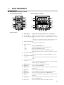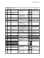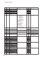
1
No. CP-SP-1265E
SDC45/46
Digital Indicating Controller
User's Manual
for
Displays and Settings
Thank you for purchasing the SDC45/46
Digital Indicating Controller.
This manual contains a complete list of
SDC45/46 displays and settings. For
assistance in correctly setting the
SDC45/46, keep this manual nearby for
handy reference.
For details about how to change the settings, refer to the installation and configuration manual (CP-SP-1218E) for the
SDC45/46.
RESTRICTIONS ON USE
This product has been designed, developed and manufactured for general-purpose
application in machinery and equipment.
Accordingly, when used in applications outlined below, special care should be taken to
implement a fail-safe and/or redundant design concept as well as a periodic
maintenance program.
• Safety devices for plant worker protection
• Start/stop control devices for transportation and material handling machines
• Aeronautical/aerospace machines
• Control devices for nuclear reactors
Never use this product in applications where human safety may be put at risk.
NOTICE
Be sure that the user receives this manual before the product is used.
Copying or duplicating this user’s manual in part or in whole is forbidden. The information and specifications in this manual are subject to
change without notice.
Considerable effort has been made to ensure that this manual is free
from inaccuracies and omissions. If you should find an error or omission, please contact Yamatake Corporation.
In no event is Yamatake Corporation liable to anyone for any indirect,
special or consequential damages as a result of using this product.
©2007 Yamatake Corporation ALL RIGHTS RESERVED
The Role of This Manual
A total of 4 different manuals are available for the SDC45/46. Read them as necessary for your specific requirements. If a manual you require is not available, contact Yamatake Corporation or its dealer.
C P-U
U
3E
M-012
nual
ser's Ma
G
WARNIN
N
CAUTIO
WARN
CAU TI
ING
ON
SDC45/46 Digital Indicating Controller Installation Instructions
Manual No. CP-UM-5445E
This manual is supplied with the SDC45/46. Personnel in charge of design
and/or manufacture of a system using the SDC45/46 must thoroughly read
this manual. This manual describes the safety precautions, installation,
wiring, primary specifications, and transitions of key operations and displays.
For further information about operation, refer to another manual, Installation
and Configuration.
SDC45/46 Digital Indicating Controller User's Manual for Displays and
Settings
Manual No. CP-SP-1265E
This manual. The manual is a reference document necessary to set or
change data. The manual lists up the displays, setup items, setting ranges,
and initial values.
SDC45/46 Digital Indicating Controller User's Manual for Installation
and Configuration
Manual No. CP-SP-1218E
Personnel in charge of design, manufacture, operation, and/or maintenance
of a system using SDC45/46 must thoroughly read this manual. This manual
also describes the installation, wiring, connections for communication, all
functions and settings of the SDC45/46, operating procedures, troubleshooting, and detailed specifications.
SLP-C45 Smart Loader Package for SDC45/46 Digital Indicating
Controller
Manual No. CP-UM-5458E
This manual is supplied with the SLP-C45 Smart Loader Package. The manual describes the software used to make various settings for SDC45/46 using
a personal computer. Personnel in charge of design or setting of a system
using SDC45/46 must thoroughly read this manual. The manual describes
installation of the software into a personal computer, operation of the personal computer, various functions, and setup procedures.
i
Contents
The Role of This Manual
1.
PRELIMINARIES
■
■
2.
Names and function of parts • • • • • • • • • • • • • • • • • • • • • • • • • • • • • • • • • • • • • • • • • • • • • • • 1-1
Method of key operations • • • • • • • • • • • • • • • • • • • • • • • • • • • • • • • • • • • • • • • • • • • • • • • • • • 1-2
PARA BANK SETTINGS
■
■
■
■
■
■
■
■
■
■
■
■
■
■
■
■
■
■
■
■
■
■
■
■
■
■
■
Mode bank (MOde) • • • • • • • • • • • • • • • • • • • • • • • • • • • • • • • • • • • • • • • • • • • • • • • • • • • • • • • • • 2-1
Loop 1 PID bank (l i.pi d) • • • • • • • • • • • • • • • • • • • • • • • • • • • • • • • • • • • • • • • • • • • • • • • • • • 2-1
Loop 2 PID bank (l2.pi d) • • • • • • • • • • • • • • • • • • • • • • • • • • • • • • • • • • • • • • • • • • • • • • • • • • 2-4
SP configuration bank (Spcnf) • • • • • • • • • • • • • • • • • • • • • • • • • • • • • • • • • • • • • • • • • • • • 2-7
Event configuration bank (evcnf) • • • • • • • • • • • • • • • • • • • • • • • • • • • • • • • • • • • • • • • • • 2-8
Control bank (ctrl) • • • • • • • • • • • • • • • • • • • • • • • • • • • • • • • • • • • • • • • • • • • • • • • • • • • • • • • 2-11
MV bank (Mv) • • • • • • • • • • • • • • • • • • • • • • • • • • • • • • • • • • • • • • • • • • • • • • • • • • • • • • • • • • • • • 2-13
Setup bank (Setup) • • • • • • • • • • • • • • • • • • • • • • • • • • • • • • • • • • • • • • • • • • • • • • • • • • • • • • • 2-14
Priority bank (prI Or) • • • • • • • • • • • • • • • • • • • • • • • • • • • • • • • • • • • • • • • • • • • • • • • • • • • • • 2-15
PV bank (pv) • • • • • • • • • • • • • • • • • • • • • • • • • • • • • • • • • • • • • • • • • • • • • • • • • • • • • • • • • • • • • • 2-16
Output bank (Out) • • • • • • • • • • • • • • • • • • • • • • • • • • • • • • • • • • • • • • • • • • • • • • • • • • • • • • • • 2-18
Posion proportional bank (PP) • • • • • • • • • • • • • • • • • • • • • • • • • • • • • • • • • • • • • • • • • • • • 2-20
CT input bank (CT) • • • • • • • • • • • • • • • • • • • • • • • • • • • • • • • • • • • • • • • • • • • • • • • • • • • • • • • • 2-20
AC input bank (AC)• • • • • • • • • • • • • • • • • • • • • • • • • • • • • • • • • • • • • • • • • • • • • • • • • • • • • • • • 2-20
Linearization table bank (tbl) • • • • • • • • • • • • • • • • • • • • • • • • • • • • • • • • • • • • • • • • • • • • • 2-21
Internal contact input bank (i C) • • • • • • • • • • • • • • • • • • • • • • • • • • • • • • • • • • • • • • • • • • 2-26
Digital output bank (dO) • • • • • • • • • • • • • • • • • • • • • • • • • • • • • • • • • • • • • • • • • • • • • • • • • • 2-28
Logical operation bank (bf) • • • • • • • • • • • • • • • • • • • • • • • • • • • • • • • • • • • • • • • • • • • • • • 2-29
User-defined bank (udb) • • • • • • • • • • • • • • • • • • • • • • • • • • • • • • • • • • • • • • • • • • • • • • • • • • 2-32
Temperature and pressure compensation bank (PV.CMP) • • • • • • • • • • • • • • • • • 2-32
Input operation bank (In.FNC) • • • • • • • • • • • • • • • • • • • • • • • • • • • • • • • • • • • • • • • • • • • • • 2-33
Output operation bank (OT.FNC) • • • • • • • • • • • • • • • • • • • • • • • • • • • • • • • • • • • • • • • • • • 2-35
Display/key bank (HMI) • • • • • • • • • • • • • • • • • • • • • • • • • • • • • • • • • • • • • • • • • • • • • • • • • • • • 2-37
RS-485 communication bank (rS485) • • • • • • • • • • • • • • • • • • • • • • • • • • • • • • • • • • • • 2-38
Lock bank (lOcK) • • • • • • • • • • • • • • • • • • • • • • • • • • • • • • • • • • • • • • • • • • • • • • • • • • • • • • • • • 2-38
Monitor bank (MOni) • • • • • • • • • • • • • • • • • • • • • • • • • • • • • • • • • • • • • • • • • • • • • • • • • • • • • • • 2-40
Instrument information bank (i d)• • • • • • • • • • • • • • • • • • • • • • • • • • • • • • • • • • • • • • • • • 2-43
ii
3.
SP/EV BANK SETTINGS
■
■
■
■
■
■
■
4.
SP group selection bank (SpnO) • • • • • • • • • • • • • • • • • • • • • • • • • • • • • • • • • • • • • • • • • • • 3-1
Loop 1 multi-SP bank (l 1.lSp) • • • • • • • • • • • • • • • • • • • • • • • • • • • • • • • • • • • • • • • • • • • • • 3-1
Loop 2 multi-SP bank (l2.lSp) • • • • • • • • • • • • • • • • • • • • • • • • • • • • • • • • • • • • • • • • • • • • • 3-2
Loop 1 recipe bank (l 1.rec) • • • • • • • • • • • • • • • • • • • • • • • • • • • • • • • • • • • • • • • • • • • • • • • 3-3
Loop 2 recipe bank (l2.rec) • • • • • • • • • • • • • • • • • • • • • • • • • • • • • • • • • • • • • • • • • • • • • • 3-11
RSP bank (rSp) • • • • • • • • • • • • • • • • • • • • • • • • • • • • • • • • • • • • • • • • • • • • • • • • • • • • • • • • • • • 3-19
Event setup bank (ev) • • • • • • • • • • • • • • • • • • • • • • • • • • • • • • • • • • • • • • • • • • • • • • • • • • • • 3-19
STANDARD BIT CODES AND STANDARD NUMERICAL CODES
■
■
Standard bit codes• • • • • • • • • • • • • • • • • • • • • • • • • • • • • • • • • • • • • • • • • • • • • • • • • • • • • • • • • 4-1
Standard numerical codes • • • • • • • • • • • • • • • • • • • • • • • • • • • • • • • • • • • • • • • • • • • • • • • • • 4-2
iii
1.
PRELIMINARIES
■ Names and function of parts
● Front panel of SDC45
● Front panel of SDC46
(7)
(5)
(1)
(6)
(5)
(3)
(7)
(5)
(1)
(3)
(2)
(6)
(2)
(8)
(9)
(4)
(11)
(9)
(5)
(4)
(11)
(10)
(13)
(10)
(13)
(12)
(17)
(12)
(17)
(16) (15)
(16) (15) (14) (14) (8)
● Description
(1) Upper display:
Displays PV (present temperature etc.) or setup items.
(2) Lower display:
Displays SP (set temperature, etc.) and other parameters.
(3) Auxiliary display: Displays group No., loop* No., and channel No. of setup
item.
*: The series of connections from PV input to PID operation
through to control output is generically called a loop.
(4) Multi-status indicator:
Indicates MV or DI/DO status.
(5) Mode indicators:
rdy:
Lights up in READY mode.
rsp:
Lights up in RSP (remote setting input) mode.
man:
Lights up in MANUAL mode.
out1-7:
Light up when the output is ON (SDC45: out1-5).
Always lit when the output is current or continuous voltage.
(6) User function indicators:
uf1-4:
Light under user-assigned conditions (SDC45: uf1, uf2).
(7) Loop number indicators:
pv1, pv2:
Light up to indicate which loop has the displayed PV
value.
(8) [ ], [ ],[<], [>] keys:
Used to increment/decrement numeric values and shift
between digits or settable items.
(9) [auto/man] key: Used to change AUTO/MANUAL mode.
(10) [sp/ev] key:
Used to set the SP/EV bank.
(11) [display] key:
Used to change the display contents in the operation display mode.
(12) [para] key:
Used to set the PARA bank.
(13) [enter] key:
Used in initiating setup and to confirm changed values.
(14) [f1], [f2] key:
Used for user-assigned functions. (SDC46 only).
(15) [at] key:
Used to execute/cancel auto-tuning, or for user-assigned
functions.
(16) [rsp/lsp] key:
Used to change between remote and local set point, or for
user-assigned functions.
(17) Loader jack:
Jack for connection of PC loader cable (with cap).
1-1
1. PRELIMINARIES
■ Method of key operations
● Key operations when setting PARA bank
(1) Press the [display] key to return to the operation display.
(2) To select a bank, keep the [para] key pressed for 2 s.
(3) To display a bank to be set, press the [para] key, [
] key, or [
] key.
(4) When a desired bank is displayed, press the [enter] key.
(5) To display an item to be set, press the [para] key, [
or [ ] key.
] key, [
] key, [
] key,
(6) When a desired item is displayed, press the [enter] key.
(7) Change the set value with the [
] key, [
] key, [
] key, or [
] key.
(8) To set the set value you have changed, press the [enter] key.
(9) To set other items in the same bank, repeat the operation from step (5).
To set desired set data in other bank, continue the operation from step (2).
(10)To exit the setting, press the [display] key.
● Key operations when setting SP/EV bank
(1) Press the [display] key to return to the operation display.
(2) To select a bank, keep the [sp/ev] key pressed for 2 s.
(3) To display a bank to be set, press the [sp/ev] key, [
] key, or [
] key.
(4) When a desired bank is displayed, press the [enter] key.
(5) To display an item to be set, press the [sp/ev] key, [
or [ ] key.
] key, [
] key, [
] key,
(6) When a desired item is displayed, press the [enter] key.
(7) Change the set value with the [
] key, [
] key, [
] key, or [
] key.
(8) To set the set value you have changed, press the [enter] key.
(9) To set other items in the same bank, repeat the operation from step (5).
To set desired set data in other bank, continue the operation from step (2).
(10)To exit the setting, press the [display] key.
1-2
2.
PARA BANK SETTINGS
■ Mode bank (MODE)
Item
Display Loop number
(auxiliary display)
r---r
L. 1.
RUN/READY
A---M
L. 1.
AUTO/MANUAL
At
L. 1.
Auto tuning (AT) stop/start
L---r
L. 1.
LSP/RSP
Cb
L. 1.
Backup/Through output
r---r
L.2.
RUN/READY
A---M
L.2.
AUTO/MANUAL
At
L.2.
Auto tuning (AT) stop/start
L---r
L.2.
LSP/RSP
Cb
L.2.
(Reserved for future use)
Settings and descriptions
rUn
rdy
AutO
Man
At.Of
At.On
lSp
rSp
lMv
rMv
rUn
rdy
AutO
Man
At.Of
At.On
lSp
rSp
: RUN mode
: READY mode
: AUTO mode
: MANUAL mode
: AT stop
: AT start
: LSP mode
: RSP mode
: Backup mode (local MV)
: Through output mode (remote MV)
: RUN mode
: READY mode
: AUTO mode
: MANUAL mode
: AT stop
: AT start
: LSP mode
: RSP mode
Initial User
value setting
RUN
Remarks
AUTO
AT.OF
LSP
LMV
RUN
AUTO
AT.OF
LSP
-
Setting is disabled.
■ Loop 1 PID bank (L 1.PI D)
Display Loop number
Item
(auxiliary display)
p-0 1
L. 1.
Proportional band
1-0 1
L. 1.
Integral time
d-0 1
L. 1.
Derivative time
OL-0 1
Oh-0 1
re-0 1
p-0 1c
i-0 1c
L. 1.
L. 1.
L. 1.
L. 1.
L. 1.
Output low limit
Output high limit
Manual reset
Proportional band for cool side
Integral time for cool side
d-0 1
L. 1.
Derivative time for cool
side
OL.0 1C
OH.0 1C
P-02
I -02
d-02
OL-02
OH-02
rE-02
P-02C
I -02C
d-02C
OL.02C
OH.02C
P-03
I -03
d-03
OL-03
OH-03
rE-03
P-03C
I -03C
d-03C
OL.03C
OH.03C
L. 1.
L. 1.
L. 1.
L. 1.
L. 1.
L. 1.
L. 1.
L. 1.
L. 1.
L. 1.
L. 1.
L. 1.
L. 1.
L. 1.
L. 1.
L. 1.
L. 1.
L. 1.
L. 1.
L. 1.
L. 1.
L. 1.
L. 1.
L. 1.
Output low limit for cool side
Output high limit for cool side
Proportional band
Integral time
Derivative time
Output low limit
Output high limit
Manual reset
Proportional band for cool side
Integral time for cool side
Derivative time for cool side
Output low limit for cool side
Output high limit for cool side
Proportional band
Integral time
Derivative time
Output low limit
Output high limit
Manual reset
Proportional band for cool side
Integral time for cool side
Derivative time for cool side
Output low limit for cool side
Output high limit for cool side
PID
Settings and descriptions
value
1
0.1 to 3200.0 %
1
0 to 32000 s, 0.0 to 3200.0 s or 0.00 to
320.00 s (no integral control action when
set at 0, 0.0 or 0.00.)
1
0 to 32000 s, 0.0 to 3200.0 s or 0.00 to
320.00 s (no derivative control action when
set at 0, 0.0 or 0.00.)
1
-10.0 to +110.0 %
1
1
1
0.1 to 3200.0 %
1
0 to 32000 s, 0.0 to 3200.0 s or 0.00 to
320.00 s (no integral control action when
set at 0, 0.0 or 0.00.)
1
0 to 32000 s, 0.0 to 3200.0 s or 0.00 to
320.00 s (no derivative control action when
set at 0, 0.0 or 0.00.)
1
-10.0 to +110.0 %
1
2
Same as PID1
2
2
2
2
2
2
2
2
2
2
3
Same as PID1
3
3
3
3
3
3
3
3
3
3
Initial User
Remarks
value setting
5.0
120
The decimal point position is
determined by the decimal point
positions for the integral time and
derivative time.
30
0.0
100.0
50.0
5.0
120
30
0.0
100.0
5.0
120
30
0.0
100.0
50.0
5.0
120
30
0.0
100.0
5.0
120
30
0.0
100.0
50.0
5.0
120
30
0.0
100.0
The decimal point position is
determined by the decimal point
positions for the integral time and
derivative time.
Same as PID1
Same as PID1
2-1
2. PARA BANK SETTINGS
Display Loop number
(auxiliary display)
P-04
L. 1.
I -04
L. 1.
d-04
L. 1.
OL-04
L. 1.
OH-04
L. 1.
rE-04
L. 1.
P-04C
L. 1.
I -04C
L. 1.
d-04C
L. 1.
OL.04C
L. 1.
OH.04C
L. 1.
P-05
L. 1.
I -05
L. 1.
d-05
L. 1.
OL-05
L. 1.
OH-05
L. 1.
rE-05
L. 1.
P-05C
L. 1.
I -05C
L. 1.
d-05C
L. 1.
OL.05C
L. 1.
OH.05C
L. 1.
P-06
L. 1.
I -06
L. 1.
d-06
L. 1.
OL-06
L. 1.
OH-06
L. 1.
rE-06
L. 1.
P-06C
L. 1.
I -06C
L. 1.
d-06C
L. 1.
OL.06C
L. 1.
OH.06C
L. 1.
P-07
L. 1.
I -07
L. 1.
d-07
L. 1.
OL-07
L. 1.
OH-07
L. 1.
rE-07
L. 1.
P-07C
L. 1.
I -07C
L. 1.
d-07C
L. 1.
OL.07C
L. 1.
OH.07C
L. 1.
P-08
L. 1.
I -08
L. 1.
d-08
L. 1.
OL-08
L. 1.
OH-08
L. 1.
rE-08
L. 1.
P-08C
L. 1.
I -08C
L. 1.
d-08C
L. 1.
OL.08C
L. 1.
OH.08C
L. 1.
P-09
L. 1.
I -09
L. 1.
d-09
L. 1.
OL-09
L. 1.
OH-09
L. 1.
rE-09
L. 1.
P-09C
L. 1.
I -09C
L. 1.
d-09C
L. 1.
OL.09C
L. 1.
OH.09C
L. 1.
2-2
Item
Proportional band
Integral time
Derivative time
Output low limit
Output high limit
Manual reset
Proportional band for cool side
Integral time for cool side
Derivative time for cool side
Output low limit for cool side
Output high limit for cool side
Proportional band
Integral time
Derivative time
Output low limit
Output high limit
Manual reset
Proportional band for cool side
Integral time for cool side
Derivative time for cool side
Output low limit for cool side
Output high limit for cool side
Proportional band
Integral time
Derivative time
Output low limit
Output high limit
Manual reset
Proportional band for cool side
Integral time for cool side
Derivative time for cool side
Output low limit for cool side
Output high limit for cool side
Proportional band
Integral time
Derivative time
Output low limit
Output high limit
Manual reset
Proportional band for cool side
Integral time for cool side
Derivative time for cool side
Output low limit for cool side
Output high limit for cool side
Proportional band
Integral time
Derivative time
Output low limit
Output high limit
Manual reset
Proportional band for cool side
Integral time for cool side
Derivative time for cool side
Output low limit for cool side
Output high limit for cool side
Proportional band
Integral time
Derivative time
Output low limit
Output high limit
Manual reset
Proportional band for cool side
Integral time for cool side
Derivative time for cool side
Output low limit for cool side
Output high limit for cool side
PID
value
4
4
4
4
4
4
4
4
4
4
4
5
5
5
5
5
5
5
5
5
5
5
6
6
6
6
6
6
6
6
6
6
6
7
7
7
7
7
7
7
7
7
7
7
8
8
8
8
8
8
8
8
8
8
8
9
9
9
9
9
9
9
9
9
9
9
Settings and descriptions
Same as PID1
Same as PID1
Same as PID1
Same as PID1
Same as PID1
Same as PID1
Initial User
Remarks
value setting
5.0
Same as PID1
120
30
0.0
100.0
50.0
5.0
120
30
0.0
100.0
5.0
Same as PID1
120
30
0.0
100.0
50.0
5.0
120
30
0.0
100.0
5.0
Same as PID1
120
30
0.0
100.0
50.0
5.0
120
30
0.0
100.0
5.0
Same as PID1
120
30
0.0
100.0
50.0
5.0
120
30
0.0
100.0
5.0
Same as PID1
120
30
0.0
100.0
50.0
5.0
120
30
0.0
100.0
5.0
Same as PID1
120
30
0.0
100.0
50.0
5.0
120
30
0.0
100.0
2. PARA BANK SETTINGS
Display Loop number
(auxiliary display)
P- 10
L. 1.
I - 10
L. 1.
d- 10
L. 1.
OL- 10
L. 1.
OH- 10
L. 1.
rE- 10
L. 1.
P- 10C
L. 1.
I - 10C
L. 1.
d- 10C
L. 1.
OL. 10C
L. 1.
OH. 10C
L. 1.
P- 1 1
L. 1.
I-11
L. 1.
d- 1 1
L. 1.
OL- 1 1
L. 1.
OH- 1 1
L. 1.
rE- 1 1
L. 1.
P- 1 1C
L. 1.
I - 1 1C
L. 1.
d- 1 1C
L. 1.
OL. 1 1C
L. 1.
OH. 1 1C
L. 1.
P- 12
L. 1.
I - 12
L. 1.
d- 12
L. 1.
OL- 12
L. 1.
OH- 12
L. 1.
rE- 12
L. 1.
P- 12C
L. 1.
I - 12C
L. 1.
d- 12C
L. 1.
OL. 12C
L. 1.
OH. 12C
L. 1.
P- 13
L. 1.
I - 13
L. 1.
d- 13
L. 1.
OL- 13
L. 1.
OH- 13
L. 1.
rE- 13
L. 1.
P- 13C
L. 1.
I - 13C
L. 1.
d- 13C
L. 1.
OL. 13C
L. 1.
OH. 13C
L. 1.
P- 14
L. 1.
I - 14
L. 1.
d- 14
L. 1.
OL- 14
L. 1.
OH- 14
L. 1.
rE- 14
L. 1.
P- 14C
L. 1.
I - 14C
L. 1.
d- 14C
L. 1.
OL. 14C
L. 1.
OH. 14C
L. 1.
P- 15
L. 1.
I - 15
L. 1.
d- 15
L. 1.
OL- 15
L. 1.
OH- 15
L. 1.
rE- 15
L. 1.
P- 15C
L. 1.
I - 15C
L. 1.
d- 15C
L. 1.
OL. 15C
L. 1.
OH. 15C
L. 1.
Item
Proportional band
Integral time
Derivative time
Output low limit
Output high limit
Manual reset
Proportional band for cool side
Integral time for cool side
Derivative time for cool side
Output low limit for cool side
Output high limit for cool side
Proportional band
Integral time
Derivative time
Output low limit
Output high limit
Manual reset
Proportional band for cool side
Integral time for cool side
Derivative time for cool side
Output low limit for cool side
Output high limit for cool side
Proportional band
Integral time
Derivative time
Output low limit
Output high limit
Manual reset
Proportional band for cool side
Integral time for cool side
Derivative time for cool side
Output low limit for cool side
Output high limit for cool side
Proportional band
Integral time
Derivative time
Output low limit
Output high limit
Manual reset
Proportional band for cool side
Integral time for cool side
Derivative time for cool side
Output low limit for cool side
Output high limit for cool side
Proportional band
Integral time
Derivative time
Output low limit
Output high limit
Manual reset
Proportional band for cool side
Integral time for cool side
Derivative time for cool side
Output low limit for cool side
Output high limit for cool side
Proportional band
Integral time
Derivative time
Output low limit
Output high limit
Manual reset
Proportional band for cool side
Integral time for cool side
Derivative time for cool side
Output low limit for cool side
Output high limit for cool side
PID
value
10
10
10
10
10
10
10
10
10
10
10
11
11
11
11
11
11
11
11
11
11
11
12
12
12
12
12
12
12
12
12
12
12
13
13
13
13
13
13
13
13
13
13
13
14
14
14
14
14
14
14
14
14
14
14
15
15
15
15
15
15
15
15
15
15
15
Settings and descriptions
Same as PID1
Same as PID1
Same as PID1
Same as PID1
Same as PID1
Same as PID1
Initial User
Remarks
value setting
5.0
Same as PID1
120
30
0.0
100.0
50.0
5.0
120
30
0.0
100.0
5.0
Same as PID1
120
30
0.0
100.0
50.0
5.0
120
30
0.0
100.0
5.0
Same as PID1
120
30
0.0
100.0
50.0
5.0
120
30
0.0
100.0
5.0
Same as PID1
120
30
0.0
100.0
50.0
5.0
120
30
0.0
100.0
5.0
Same as PID1
120
30
0.0
100.0
50.0
5.0
120
30
0.0
100.0
5.0
Same as PID1
120
30
0.0
100.0
50.0
5.0
120
30
0.0
100.0
2-3
2. PARA BANK SETTINGS
Display Loop number
(auxiliary display)
P- 16
L. 1.
I- 16
L. 1.
d- 16
L. 1.
OL- 16
L. 1.
OH- 16
L. 1.
rE- 16
L. 1.
P- 16C
L. 1.
I - 16C
L. 1.
d- 16C
L. 1.
OL. 16C
L. 1.
OH. 16C
L. 1.
Item
PID
Settings and descriptions
value
Proportional band
16 Same as PID1
Integral time
16
Derivative time
16
Output low limit
16
Output high limit
16
Manual reset
16
Proportional band for cool side 16
Integral time for cool side
16
Derivative time for cool side
16
Output low limit for cool side
16
Output high limit for cool side 16
Initial User
Remarks
value setting
5.0
Same as PID1
120
30
0.0
100.0
50.0
5.0
120
30
0.0
100.0
■ Loop 2 PID bank (L2.PI D)
Display Loop number
Item
(Auxiliary display)
P-0 1
L.2.
Proportional band
I -0 1
L.2.
Integral time
d-0 1
L.2.
Derivative time
OL-0 1
OH-0 1
rE-0 1
P-0 1C
I -0 1C
L.2.
L.2.
L.2.
L.2.
L.2.
Output low limit
Output high limit
Manual reset
Proportional band for cool side
Integral time for cool side
d-0 1C
L.2.
Derivative time for cool side
OL.0 1C
OH.0 1C
P-02
I -02
d-02
OL-02
OH-02
rE-02
P-02C
I -02C
d-02C
OL.02C
OH.02C
P-03
I -03
d-03
OL-03
OH-03
rE-03
P-03C
I -03C
d-03C
OL.03C
OH.03C
P-04
I -04
d-04
OL-04
OH-04
rE-04
P-04C
I -04C
d-04C
OL.04C
OH.04C
L.2.
L.2.
L.2.
L.2.
L.2.
L.2.
L.2.
L.2.
L.2.
L.2.
L.2.
L.2.
L.2.
L.2.
L.2.
L.2.
L.2.
L.2.
L.2.
L.2.
L.2.
L.2.
L.2.
L.2.
L.2.
L.2.
L.2.
L.2.
L.2.
L.2.
L.2.
L.2.
L.2.
L.2.
L.2.
Output low limit for cool side
Output high limit for cool side
Proportional band
Integral time
Derivative time
Output low limit
Output high limit
Manual reset
Proportional band for cool side
Integral time for cool side
Derivative time for cool side
Output low limit for cool side
Output high limit for cool side
Proportional band
Integral time
Derivative time
Output low limit
Output high limit
Manual reset
Proportional band for cool side
Integral time for cool side
Derivative time for cool side
Output low limit for cool side
Output high limit for cool side
Proportional band
Integral time
Derivative time
Output low limit
Output low limit
Manual reset
Proportional band for cool side
Integral time for cool side
Derivative time for cool side
Output low limit for cool side
Output high limit for cool side
2-4
PID
Settings and descriptions
value
1
0.1 to 3200.0 %
1
0 to 32000 s, 0.0 to 3200.0 s or 0.00 to
320.00 s (no integral control action when
set at 0, 0.0 or 0.00)
1
0 to 32000 s, 0.0 to 3200.0 s or 0.00 to
320.00 s (no derivative control action when
set at 0, 0.0 or 0.00)
1
-10.0 to +110.0 %
1
1
1
0.1 to 3200.0 %
1
0 to 32000 s, 0.0 to 3200.0 s or 0.00 to
320.00 s (no integral control action when
set at 0, 0.0 or 0.00)
1
0 to 32000 s, 0.0 to 3200.0 s or 0.00 to
320.00 s (no derivative control action when
set at 0, 0.0 or 0.00)
1
-10.0 to +110.0 %
1
2
Same as PID1
2
2
2
2
2
2
2
2
2
2
3
Same as PID1
3
3
3
3
3
3
3
3
3
3
4
Same as PID1
4
4
4
4
4
4
4
4
4
4
Initial User
Remarks
value setting
5.0
120
The decimal point position is
determined by the decimal point
positions for the integral time and
derivative time.
30
0.0
100.0
50.0
5.0
120
30
0.0
100.0
5.0
120
30
0.0
100.0
50.0
5.0
120
30
0.0
100.0
5.0
120
30
0.0
100.0
50.0
5.0
120
30
0.0
100.0
5.0
120
30
0.0
100.0
50.0
5.0
120
30
0.0
100.0
The decimal point position is
determined by the decimal point
positions for the integral time and
derivative time.
Same as PID1
Same as PID1
Same as PID1
2. PARA BANK SETTINGS
Display Loop number
(auxiliary display)
P-05
L.2.
I -05
L.2.
d-05
L.2.
OL-05
L.2.
OH-05
L.2.
rE-05
L.2.
P-05C
L.2.
I -05C
L.2.
d-05C
L.2.
OL.05C
L.2.
OH.05C
L.2.
P-06
L.2.
I -06
L.2.
d-06
L.2.
OL-06
L.2.
OH-06
L.2.
rE-06
L.2.
P-06C
L.2.
I -06C
L.2.
d-06C
L.2.
OL.06C
L.2.
OH.06C
L.2.
P-07
L.2.
I -07
L.2.
d-07
L.2.
OL-07
L.2.
OH-07
L.2.
rE-07
L.2.
P-07C
L.2.
I -07C
L.2.
d-07C
L.2.
OL.07C
L.2.
OH.07C
L.2.
P-08
L.2.
I -08
L.2.
d-08
L.2.
OL-08
L.2.
OH-08
L.2.
rE-08
L.2.
P-08C
L.2.
I -08C
L.2.
d-08C
L.2.
OL.08C
L.2.
OH.08C
L.2.
P-09
L.2.
I -09
L.2.
d-09
L.2.
OL-09
L.2.
OH-09
L.2.
rE-09
L.2.
P-09C
L.2.
I -09C
L.2.
d-09C
L.2.
OL.09C
L.2.
OH.09C
L.2.
P- 10
L.2.
I - 10
L.2.
d- 10
L.2.
OL- 10
L.2.
OH- 10
L.2.
rE- 10
L.2.
P- 10C
L.2.
I - 10C
L.2.
d- 10C
L.2.
OL. 10C
L.2.
OH. 10C
L.2.
Item
Proportional band
Integral time
Derivative time
Output low limit
Output high limit
Manual reset
Proportional band for cool side
Integral time for cool side
Derivative time for cool side
Output low limit for cool side
Output high limit for cool side
Proportional band
Integral time
Derivative time
Output low limit
Output high limit
Manual reset
Proportional band for cool side
Integral time for cool side
Derivative time for cool side
Output low limit for cool side
Output high limit for cool side
Proportional band
Integral time
Derivative time
Output low limit
Output high limit
Manual reset
Proportional band for cool side
Integral time for cool side
Derivative time for cool side
Output low limit for cool side
Output high limit for cool side
Proportional band
Integral time
Derivative time
Output low limit
Output high limit
Manual reset
Proportional band for cool side
Integral time for cool side
Derivative time for cool side
Output low limit for cool side
Output high limit for cool side
Proportional band
Integral time
Derivative time
Output low limit
Output high limit
Manual reset
Proportional band for cool side
Integral time for cool side
Derivative time for cool side
Output low limit for cool side
Output high limit for cool side
Proportional band
Integral time
Derivative time
Output low limit
Output high limit
Manual reset
Proportional band for cool side
Integral time for cool side
Derivative time for cool side
Output low limit for cool side
Output high limit for cool side
PID
value
5
5
5
5
5
5
5
5
5
5
5
6
6
6
6
6
6
6
6
6
6
6
7
7
7
7
7
7
7
7
7
7
7
8
8
8
8
8
8
8
8
8
8
8
9
9
9
9
9
9
9
9
9
9
9
10
10
10
10
10
10
10
10
10
10
10
Settings and descriptions
Same as PID1
Same as PID1
Same as PID1
Same as PID1
Same as PID1
Same as PID1
Initial User
Remarks
value setting
5.0
Same as PID1
120
30
0.0
100.0
50.0
5.0
120
30
0.0
100.0
5.0
Same as PID1
120
30
0.0
100.0
50.0
5.0
120
30
0.0
100.0
5.0
Same as PID1
120
30
0.0
100.0
50.0
5.0
120
30
0.0
100.0
5.0
Same as PID1
120
30
0.0
100.0
50.0
5.0
120
30
0.0
100.0
5.0
Same as PID1
120
30
0.0
100.0
50.0
5.0
120
30
0.0
100.0
5.0
Same as PID1
120
30
0.0
100.0
50.0
5.0
120
30
0.0
100.0
2-5
2. PARA BANK SETTINGS
Display Loop number
(auxiliary display)
P- 1 1
L.2.
I-11
L.2.
d- 1 1
L.2.
OL- 1 1
L.2.
OH- 1 1
L.2.
rE- 1 1
L.2.
P- 1 1C
L.2.
I - 1 1C
L.2.
d- 1 1C
L.2.
OL. 1 1C
L.2.
OH. 1 1C
L.2.
P- 12
L.2.
I - 12
L.2.
d- 12
L.2.
OL- 12
L.2.
OH- 12
L.2.
rE- 12
L.2.
P- 12C
L.2.
I - 12C
L.2.
d- 12C
L.2.
OL. 12C
L.2.
OH. 12C
L.2.
P- 13
L.2.
I - 13
L.2.
d- 13
L.2.
OL- 13
L.2.
OH- 13
L.2.
rE- 13
L.2.
P- 13C
L.2.
I - 13C
L.2.
d- 13C
L.2.
OL. 13C
L.2.
OH. 13C
L.2.
P- 14
L.2.
I - 14
L.2.
d- 14
L.2.
OL- 14
L.2.
OH- 14
L.2.
rE- 14
L.2.
P- 14C
L.2.
I - 14C
L.2.
d- 14C
L.2.
OL. 14C
L.2.
OH. 14C
L.2.
P- 15
L.2.
I - 15
L.2.
d- 15
L.2.
OL- 15
L.2.
OH- 15
L.2.
rE- 15
L.2.
P- 15C
L.2.
I - 15C
L.2.
d- 15C
L.2.
OL. 15C
L.2.
OH. 15C
L.2.
P- 16
L.2.
I - 16
L.2.
d- 16
L.2.
OL- 16
L.2.
OH- 16
L.2.
rE- 16
L.2.
P- 16C
L.2.
I - 16C
L.2.
d- 16C
L.2.
OL. 16C
L.2.
OH. 16C
L.2.
2-6
Item
Proportional band
Integral time
Derivative time
Output low limit
Output high limit
Manual reset
Proportional band for cool side
Integral time for cool side
Derivative time for cool side
Output low limit for cool side
Output high limit for cool side
Proportional band
Integral time
Derivative time
Output low limit
Output high limit
Manual reset
Proportional band for cool side
Integral time for cool side
Derivative time for cool side
Output low limit for cool side
Output high limit for cool side
Proportional band
Integral time
Derivative time
Output low limit
Output high limit
Manual reset
Proportional band for cool side
Integral time for cool side
Derivative time for cool side
Output low limit for cool side
Output high limit for cool side
Proportional band
Integral time
Derivative time
Output low limit
Output high limit
Manual reset
Proportional band for cool side
Integral time for cool side
Derivative time for cool side
Output low limit for cool side
Output high limit for cool side
Proportional band
Integral time
Derivative time
Output low limit
Output high limit
Manual reset
Proportional band for cool side
Integral time for cool side
Derivative time for cool side
Output low limit for cool side
Output high limit for cool side
Proportional band
Integral time
Derivative time
Output low limit
Output high limit
Manual reset
Proportional band for cool side
Integral time for cool side
Derivative time for cool side
Output low limit for cool side
Output high limit for cool side
PID
value
11
11
11
11
11
11
11
11
11
11
11
12
12
12
12
12
12
12
12
12
12
12
13
13
13
13
13
13
13
13
13
13
13
14
14
14
14
14
14
14
14
14
14
14
15
15
15
15
15
15
15
15
15
15
15
16
16
16
16
16
16
16
16
16
16
16
Settings and descriptions
Same as PID1
Same as PID1
Same as PID1
Same as PID1
Same as PID1
Same as PID1
Initial User
Remarks
value setting
5.0
Same as PID1
120
30
0.0
100.0
50.0
5.0
120
30
0.0
100.0
5.0
Same as PID1
120
30
0.0
100.0
50.0
5.0
120
30
0.0
100.0
5.0
Same as PID1
120
30
0.0
100.0
50.0
5.0
120
30
0.0
100.0
5.0
Same as PID1
120
30
0.0
100.0
50.0
5.0
120
30
0.0
100.0
5.0
Same as PID1
120
30
0.0
100.0
50.0
5.0
120
30
0.0
100.0
5.0
Same as PID1
120
30
0.0
100.0
50.0
5.0
120
30
0.0
100.0
2. PARA BANK SETTINGS
■ SP configuration bank (Spcnf)
Item
Display Loop number
(auxiliary display)
LMT.0 1
L. 1.
SP low limit
LMT.02
L. 1.
SP high limit
Settings and descriptions
-19999 to +32000 U
Initial User
Remarks
value setting
-1999.9
The decimal point position is
determined by the decimal point
3200.0
positions for the loop PV/SP.
0
CSP.01
L. 1.
SP ramp unit
CSP.02
CSP.03
CSP.04
CSP.05
CSP.06
CSP.07
CSP.08
L. 1.
L. 1.
L. 1.
L. 1.
L. 1.
L. 1.
L. 1.
SP ramp-up for LSP
SP ramp-down for LSP
RSP tracking
SP ramp-up for RSP
SP ramp-down for RSP
LSP bias
RSP bias
CSP.09
CSP.10
CSP. 1 1
L. 1.
L. 1.
L. 1.
PV start for LSP
PV start for RSP
Digital RSP selection
0: PV start enabled
1: PV start disabled
0: Disabled
1: Enabled
0
0
0
CSP. 12
L. 1.
Digital RSP
SP low limit to SP high limit
0
rrA.0 1
rrA.02
rrA.03
rrA.04
rrA.05
rrA.06
rrA.07
rrA.08
LMT.0 1
LMT.02
L. 1.
L. 1.
L. 1.
L. 1.
L. 1.
L. 1.
L. 1.
L. 1.
L.2.
L.2.
RSP ratio 1
RSP ratio 2
RSP ratio 3
RSP ratio 4
RSP ratio 5
RSP ratio 6
RSP ratio 7
RSP ratio 8
SP low limit
SP high limit
0.001 to 32.000
1.000
-19999 to +32000 U
-1999.9
3200.0
CSP.0 1
L.2.
SP ramp unit
CSP.02
CSP.03
CSP.04
CSP.05
CSP.06
CSP.07
CSP.08
L.2.
L.2.
L.2.
L.2.
L.2.
L.2.
L.2.
SP ramp-up for LSP
SP ramp-down for LSP
RSP tracking
SP ramp-up for RSP
SP ramp-down for RSP
LSP bias
RSP bias
CSP.09
CSP.10
CSP.1 1
L.2.
L.2.
L.2.
PV start for LSP
PV start for RSP
Digital RSP selection
0: PV start enabled
1: PV start disabled
0: Disabled
1: Enabled
0
0
0
CSP.12
L.2.
Digital RSP
SP low limit to SP high limit
0
rrA.0 1
rrA.02
rrA.03
rrA.04
rrA.05
rrA.06
rrA.07
rrA.08
L.2.
L.2.
L.2.
L.2.
L.2.
L.2.
L.2.
L.2.
RSP ratio 1
RSP ratio 2
RSP ratio 3
RSP ratio 4
RSP ratio 5
RSP ratio 6
RSP ratio 7
RSP ratio 8
0.001 to 32.000
0: No decimal point/s
1: No decimal point/min
2: No decimal point/h 3: 0.1/s 4: 0.1/min
5: 0.1/h 6: 0.01/s 7: 0.01/min 8: 0.01/h
9: 0.001/s 10: 0.001/min 11: 0.001/h
0 U (no ramp) 1 to 32000 U
0: No tracking 1: Tracking
0 U (no ramp) 1 to 32000 U
-19999 to +32000U
0: No decimal point/s
1: No decimal point/min
2: No decimal point/h 3: 0.1/s 4: 0.1/min
5: 0.1/h 6: 0.01/s 7: 0.01/min 8: 0.01/h
9: 0.001/s 10: 0.001/min 11: 0.001/h
0 U (No ramp) 1 to 32000 U
0: No tracking 1: Tracking
0 U (No ramp) 1 to 32000 U
-19999 to +32000 U
0
0
0
0
0
0
0
The decimal point position is
determined by the SP ramp unit.
The decimal point position is
determined by the SP ramp unit.
The decimal point position is
determined by the decimal point
positions for the loop PV/SP.
SDC45A/46A/45R/46R
0: When disabled, the PV input is
used as the RSP.
SDC45V/46V
0: When disabled, the RSP
assignment is used as the RSP.
The decimal point position is
determined by the decimal point
positions for the loop PV/SP.
The decimal point position is
determined by the decimal point
positions for the loop PV/SP.
0
0
0
0
0
0
0
0
The decimal point position is
determined by the SP ramp unit.
The decimal point position is
determined by the SP ramp unit.
The decimal point position is
determined by the decimal point
positions for the loop PV/SP.
SDC45A/46A/45R/46R
0: When disabled, the PV input is
used as the RSP.
SDC45V/46V
0: When disabled, the RSP
assignment is used as the RSP.
The decimal point position is
determined by the decimal point
positions for the loop PV/SP.
1.000
2-7
2. PARA BANK SETTINGS
■ Event configuraiton bank (evcnf)
Display Event number
Item
(auxiliary display)
EP-0 1
0 1.
Operation type
EP-02
EP-03
EP-04
0 1.
0 1.
0 1.
Loop/channel definition
Direct/reverse
Standby
EP-05
EP-06
0 1.
0 1.
EVENT state at READY
Decimal point position
EP-07
0 1.
Hysteresis
EP-08
EP-09
EP-0 1
EP-02
EP-03
EP-04
EP-05
EP-06
EP-07
EP-08
EP-09
EP-0 1
EP-02
EP-03
EP-04
EP-05
EP-06
EP-07
EP-08
EP-09
EP-0 1
EP-02
EP-03
EP-04
EP-05
EP-06
EP-07
EP-08
EP-09
EP-0 1
EP-02
EP-03
EP-04
EP-05
EP-06
EP-07
EP-08
EP-09
0 1.
0 1.
02.
02.
02.
02.
02.
02.
02.
02.
02.
03.
03.
03.
03.
03.
03.
03.
03.
03.
04.
04.
04.
04.
04.
04.
04.
04.
04.
05.
05.
05.
05.
05.
05.
05.
05.
05.
ON delay
OFF delay
Operation type
Loop/channel definition
Direct/reverse
Standby
EVENT state at READY
Decimal point position
Hysteresis
ON delay
OFF delay
Operation type
Loop/channel definition
Direct/reverse
Standby
EVENT state at READY
Decimal point position
Hysteresis
ON delay
OFF delay
Operation type
Loop/channel definition
Direct/reverse
Standby
EVENT state at READY
Decimal point position
Hysteresis
ON delay
OFF delay
Operation type
Loop/channel definition
Direct/reverse
Standby
EVENT state at READY
Decimal point position
Hysteresis
ON delay
OFF delay
2-8
Settings and descriptions
Initial User
Remarks
value setting
0: No event 1: PV high limit 2: PV low limit
0
Setting range is 0 to 255.
3: PV high/low limit 4: Deviation high limit
Refer to ■ Event operation
types, polarity, hysteresis, main
5: Deviation low limit 6: Deviation high/low limit
7: Deviation high limit (final SP reference)
settings and sub settings (page
8: Deviation low limit (final SP reference)
6-5) in the installation and
configuration manual.
9: Deviation high/low limit (final SP reference)
10: SP high limit 11:SP low limit
12: SP high/low limit 13: MV high limit
14: MV low limit 15: MV high/low limit
16: MFB high/low limit 17 to 25: Undefined
26: Standard numerical bit high limit
27: Standard numerical bit low limit
28: Standard numerical bit high/low limit
29 to 60: Undefined
61: Alarm (status) 62: READY (status)
63: MANUAL(status) 64: RSP (status)
65: AT start (status)
66: During SP ramp (status)
67: Control direct action (status)
68: Through output (status) 69: Undefined
70: Timer (status)
1:Loop 1 2:Loop 2
1
Setting range is 0 to 99.
0:Direct 1: Reverse
0
0: None 1: Standby
0
2: Standby + Standby at SP change
0: Continued 1: Forced OFF
0
0: No decimal point
0
1: 1 digit after decimal point
2: 2 digits after decimal point
3: 3 digits after decimal point
4: 4 digits after decimal point
0 to 32000U
5
The decimal point position is
determined by the decimal point
position for event configuration.
0.0 to 3200.0s
0.0
0.0
Same as event 1
0
Same as event 1
1
0
0
0
0
5
0.0
0.0
Same as event 1
0
Same as event 1
1
0
0
0
0
5
0.0
0.0
Same as event 1
0
Same as event 1
1
0
0
0
0
5
0.0
0.0
Same as event 1
0
Same as event 1
1
0
0
0
0
5
0.0
0.0
2. PARA BANK SETTINGS
Display Event number
(auxiliary display)
EP-0 1
06.
EP-02
06.
EP-03
06.
EP-04
06.
EP-05
06.
EP-06
06.
EP-07
06.
EP-08
06.
EP-09
06.
EP-0 1
07.
EP-02
07.
EP-03
07.
EP-04
07.
EP-05
07.
EP-06
07.
EP-07
07.
EP-08
07.
EP-09
07.
EP-0 1
08.
EP-02
08.
EP-03
08.
EP-04
08.
EP-05
08.
EP-06
08.
EP-07
08.
EP-08
08.
EP-09
08.
EP-0 1
09.
EP-02
09.
EP-03
09.
EP-04
09.
EP-05
09.
EP-06
09.
EP-07
09.
EP-08
09.
EP-09
09.
EP-0 1
10.
EP-02
10.
EP-03
10.
EP-04
10.
EP-05
10.
EP-06
10.
EP-07
10.
EP-08
10.
EP-09
10.
EP-0 1
1 1.
EP-02
1 1.
EP-03
1 1.
EP-04
1 1.
EP-05
1 1.
EP-06
1 1.
EP-07
1 1.
EP-08
1 1.
EP-09
1 1.
EP-0 1
12.
EP-02
12.
EP-03
12.
EP-04
12.
EP-05
12.
EP-06
12.
EP-07
12.
EP-08
12.
EP-09
12.
EP-0 1
13.
EP-02
13.
EP-03
13.
EP-04
13.
EP-05
13.
Item
Operation type
Loop/channel definition
Direct/reverse
Standby
EVENT state at READY
Decimal point position
Hysteresis
ON delay
OFF delay
Operation type
Loop/channel definition
Direct/reverse
Standby
EVENT state at READY
Decimal point position
Hysteresis
ON delay
OFF delay
Operation type
Loop/channel definition
Direct/reverse
Standby
EVENT state at READY
Decimal point position
Hysteresis
ON delay
OFF delay
Operation type
Loop/channel definition
Direct/reverse
Standby
EVENT state at READY
Decimal point position
Hysteresis
ON delay
OFF delay
Operation type
Loop/channel definition
Direct/reverse
Standby
EVENT state at READY
Decimal point position
Hysteresis
ON delay
OFF delay
Operation type
Loop/channel definition
Direct/reverse
Standby
EVENT state at READY
Decimal point position
Hysteresis
ON delay
OFF delay
Operation type
Loop/channel definition
Direct/reverse
Standby
EVENT state at READY
Decimal point position
Hysteresis
ON delay
OFF delay
Operation type
Loop/channel definition
Direct/reverse
Standby
EVENT state at READY
Settings and descriptions
Same as event 1
Same as event 1
Same as event 1
Same as event 1
Same as event 1
Same as event 1
Same as event 1
Same as event 1
Initial User
Remarks
value setting
0
Same as event 1
1
0
0
0
0
5
0.0
0.0
0
Same as event 1
1
0
0
0
0
5
0.0
0.0
0
Same as event 1
1
0
0
0
0
5
0.0
0.0
0
Same as event 1
1
0
0
0
0
5
0.0
0.0
0
Same as event 1
1
0
0
0
0
5
0.0
0.0
0
Same as event 1
1
0
0
0
0
5
0.0
0.0
0
Same as event 1
1
0
0
0
0
5
0.0
0.0
0
Same as event 1
1
0
0
0
2-9
2. PARA BANK SETTINGS
Display Event number
(auxiliary display)
EP-06
13.
EP-07
13.
EP-08
13.
EP-09
13.
EP-0 1
14.
EP-02
14.
EP-03
14.
EP-04
14.
EP-05
14.
EP-06
14.
EP-07
14.
EP-08
14.
EP-09
14.
EP-0 1
15.
EP-02
15.
EP-03
15.
EP-04
15.
EP-05
15.
EP-06
15.
EP-07
15.
EP-08
15.
EP-09
15.
EP-0 1
16.
EP-02
16.
EP-03
16.
EP-04
16.
EP-05
16.
EP-06
16.
EP-07
16.
EP-08
16.
EP-09
16.
2-10
Item
Decimal point position
Hysteresis
ON delay
OFF delay
Operation type
Loop/channel definition
Direct/reverse
Standby
EVENT state at READY
Decimal point position
Hysteresis
ON delay
OFF delay
Operation type
Loop/channel definition
Direct/reverse
Standby
EVENT state at READY
Decimal point position
Hysteresis
ON delay
OFF delay
Operation type
Loop/channel definition
Direct/reverse
Standby
EVENT state at READY
Decimal point position
Hysteresis
ON delay
OFF delay
Settings and descriptions
Same as event 1
Same as event 1
Same as event 1
Same as event 1
Initial User
Remarks
value setting
0
Same as event 1
5
0.0
0.0
0
Same as event 1
1
0
0
0
0
5
0.0
0.0
0
Same as event 1
1
0
0
0
0
5
0.0
0.0
0
Same as event 1
1
0
0
0
0
5
0.0
0.0
2. PARA BANK SETTINGS
■ Control bank (ctrl)
Display Loop number
Item
(auxiliary display)
INP.0 1
L. 1.
PV assignment
INP.02
L. 1.
INP.03
Cnt.0 1
L. 1.
L. 1.
Cnt.03
L. 1.
Cnt.04
L. 1.
Cnt.05
Cnt.06
L. 1.
L. 1.
Cnt.07
L. 1.
Cnt.08
Cnt.09
Cnt. 10
L. 1.
L. 1.
L. 1.
Etd.0 1
L. 1.
Etd.02
L. 1.
Etd.03
Etd.04
L. 1.
L. 1.
Etd.05
Etd.06
Etd.07
Etd.08
Etd.09
Etd. 12
L. 1.
L. 1.
L. 1.
L. 1.
L. 1.
L. 1.
Etd. 13
Etd. 14
Etd. 15
Etd. 16
Etd. 17
Etd. 18
Etd. 19
Etd.20
INP.0 1
L. 1.
L. 1.
L. 1.
L. 1.
L. 1.
L. 1.
L. 1.
L. 1.
L. 1.
INP.02
L. 1.
INP.03
Cnt.0 1
L. 1.
L.2.
Settings and descriptions
Initial User
Remarks
value setting
0: NOP 1: PV1 (input channel)
1
Settins range is 0 to 3071.
2: PV2/21 (input channel)
For more details on the 2048 to
3: PV22 (input channel)
3071 range, see the Standard
RSP assignment
4: Results of input computation
0
numerical codes ilst (page 4-2).
5: Flowrate
Cannot be set on the SDC45A/
(corrected for temperature and pressure)
46A/45R/46R.
RMV assignment
Others
0
Loop PV/SP decimal point
0: No decimal point
1
position
1: 1 digit after decimal point
2: 2 digits after decimal point
3: 3 digits after decimal point
4: 4 digits after decimal point
Control action
0: Reverse (heat) 1: Direct (cool)
0
2: Heat/cool
Control algorithm
0: PID-A (deviation derivative) 1: Ra-PID
0
2: PID-B (PV derivative)
Control range low limit
-19999 to +32000 U
0
The decimal point position is
determined by the decimal point
Control range high limit
1000
positions for the loop PV/SP.
AT type
0: Normal (regular control characteristics)
0
1: Immediate response (control
characteristics for fast response to
external disturbance)
2: Stable (control characteristics that
minimize up/down PV fluctuation)
Heat/cool control dead zone
-100.0 to +100.0 %
0.0
Initial output of PID control
-10.0 to +110.0 %
0.0
Abnormal PV definition
0: If a PV alarm (AL01 to AL06) occurs
0
Cannot be set on the SDC45A/
1: If a PV1 alarm (AL01 or AL02) occurs
46A/45R/46R.
2: If a PV2/21 alarm (AL03 or AL04) occurs
3: If a PV22 alarm (AL05 or AL06) occurs
PID control initialization
0: Auto 1: Not initialized
0
2: Initialized (if SP value different from the
current value is input)
Integral time/derivative time
0: No decimal point
0
Affected by the decimal point
decimal point position
1: 1 digit after decimal point
positions for integral time and
2: 2 digits after decimal point
derivative time.
Output after AUTO • MANUAL change 0: Bumpless transfer 1: Preset
0
Preset MANUAL value
-10.0 to +110.0 %
0.0
When the power is turned ON,
if the operation mode is
MANUAL, the MV is preset
MANUAL value.
MV increase change limit
0.00: No limit
0.00
MV decrease change limit
0.01 to 320.00 %/s
0.00
Heat/cool selection
0: Normal 1: Energy saving
0
MV low limit at AT
-10.0 to +110.0 %
0.0
MV high limit at AT
100.0
Zone operation
0: Changed by SP value
0
When zone PID is used, set the
1: Changed by PV value
PID group selection priority to
"Zone PID function".
Zone 1
-19999 to +32000 U
3200.0
The decimal point position is
Zone 2
determined by the decimal point
Zone 3
positions for the loop PV/SP.
Zone 4
Zone 5
Zone 6
Zone 7
Zone hysteresis
0 to 32000 U
5.0
PV assignment
0: NOP 1: PV1 (input channel)
1
Settins range is 0 to 3071.
2: PV2/21 (input channel)
For more details on the 2048 to
3: PV22 (input channel)
3071 range, see the Standard
RSP assignment
4: Results of input computation
0
numerical codes ilst (page 4-2).
5: Flowrate
Cannot be set on the SDC45A/
(corrected for temperature and pressure)
46A/45R/46R.
RMV assignment
Others
0
Loop PV/SP decimal point
0: No decimal point
1
position
1: 1 digit after decimal point
2: 2 digits after decimal point
3: 3 digits after decimal point
4: 4 digits after decimal point
2-11
2. PARA BANK SETTINGS
Item
Display Loop number
(auxiliary display)
Cnt.03
L.2.
Control action
Settings and descriptions
0: Reverse (heat) 1: Direct (cool)
2: Heat/cool
0: PID-A (deviation derivative) 1: Ra-PID
2: PID-B (PV derivative)
-19999 to +32000 U
Cnt.04
L.2.
Control algorithm
Cnt.05
Cnt.06
L.2.
L.2.
Control range low limit
Control range high limit
Cnt.07
L.2.
AT type
Cnt.08
Cnt.09
Cnt. 10
L.2.
L.2.
L.2.
Etd.0 1
L.2.
Etd.02
L.2.
Etd.03
Etd.04
L.2.
L.2.
0: Normal (regular control characteristics)
1: Immediate response (control
characteristics for fast response to
external disturbance)
2: Stable (control characteristics that
minimize up/down PV fluctuation)
Heat/cool control dead zone
-100.0 to +100.0 %
Initial output of PID control
-10.0 to +110.0 %
Abnormal PV definition
0: If a PV alarm (AL01 to AL06) occurs
1: If a PV1 alarm (AL01 or AL02) occurs
2: If a PV2/21 alarm (AL03 or AL04) occurs
3: If a PV22 alarm (AL05 or AL06) occurs
PID control initialization
0: Auto 1: Not initialized
2: Initialized (if SP value different from
the current value is input)
Integration time/derivative time 0: No decimal point
decimal point position
1: 1 digit after decimal point
2: 2 digits after decimal point
Output after AUTO • MANUAL change 0: Bumpless transfer 1: Preset
Preset MANUAL value
-10.0 to +110.0 %
Etd.05
Etd.06
Etd.07
Etd.08
Etd.09
Etd. 12
L.2.
L.2.
L.2.
L.2.
L.2.
L.2.
MV increase change limit
MV decrease change limit
Heat/cool selection
MV low limit at AT
MV high limit at AT
Zone operation
Etd. 13
Etd. 14
Etd. 15
Etd. 16
Etd. 17
Etd. 18
Etd. 19
Etd.20
L.2.
L.2.
L.2.
L.2.
L.2.
L.2.
L.2.
L.2.
Zone 1
Zone 2
Zone 3
Zone 4
Zone 5
Zone 6
Zone 7
Zone hysteresis
2-12
0.00: No limit
0.01 to 320.00 %/s
0: Normal 1: Energy saving
-10.0 to +110.0 %
0: Changed by SP value
1: Changed by PV value
-19999 to +32000 U
0 to 32000 U
Initial User
value setting
0
Remarks
0
0
1000
The decimal point position is
determined by the decimal point
positions for the loop PV/SV.
0
0.0
0.0
0
Cannot be set on the SDC45A/
46A/45R/46R.
0
0
0
0.0
0.00
0.00
0
0.0
100.0
0
3200.0
5.0
Affected by the decimal point
positions for integral time and
derivative time.
When the power is turned ON,
if the operation mode is
MANUAL, the MV is the preset
MANUAL value.
When zone PID is used, set the
PID group selection priority to
"Zone PID function".
The decimal position is
determined by the decimal point
positions for the loop PV/SP.
2. PARA BANK SETTINGS
■ MV bank (Mv)
Display Loop number
(Auxiliary display)
Mv-0 1
L. 1.
Mv-02
L. 1.
Mv-03
L. 1.
Mv-04
L. 1.
Item
Output at READY
Output at READY (heat)
Output at READY (cool)
Output operation at PV alarm
Mv-05
Mv-06
Mv-07
Mv-08
Mv-09
Mv- 10
Mv- 1 1
Mv- 12
Mv- 13
CaS.0 1
CaS.02
CaS.03
L. 1.
L. 1.
L. 1.
L. 1.
L. 1.
L. 1.
L. 1.
L. 1.
L. 1.
L. 1.
L. 1.
L. 1.
Output at PV alarm
Fixed value output 1
Fixed value output 2
Fixed value output 3
Fixed value output 4
Fixed value output 5
Fixed value output 6
Fixed value output 7
Fixed value output 8
Scaling system
Scaling low limit
Scaling high limit
CaS.04
L. 1.
Tracking mode
CaS.05
CaS.06
L. 1.
L. 1.
SP output filter
SP tracking signal
TR-0 1
L. 1.
MV tracking selection
TR-02
TR-03
L. 1.
L. 1.
Reverse MV tracking signal
MV tracking signal
Mv-0 1
Mv-02
Mv-03
Mv-04
L.2.
L.2.
L.2.
L.2.
Output at READY
Output at READY (heat)
Output at READY (cool)
Output operation at PV alarm
Mv-05
Mv-06
Mv-07
Mv-08
Mv-09
Mv- 10
Mv- 1 1
Mv- 12
Mv- 13
CaS.0 1
CaS.02
CaS.03
CaS.04
CaS.05
CaS.06
TR-0 1
L.2.
L.2.
L.2.
L.2.
L.2.
L.2.
L.2.
L.2.
L.2.
L.2.
L.2.
L.2.
L.2.
L.2.
L.2.
L.2.
Output at PV alarm
Fixed value output 1
Fixed value output 2
Fixed value output 3
Fixed value output 4
Fixed value output 5
Fixed value output 6
Fixed value output 7
Fixed value output 8
Scaling system
Scaling low limit
Scaling high limit
Tracking mode
SP output filter
SP tracking signal
MV tracking selection
TR-02
TR-03
L.2.
L. 1.
Reverse MV tracking signal
MV tracking signal
Settings and descriptions
-10.0 to +110.0 %
0: Control calculations continue
1: MV is output if PV is abnormal
-10.0 to +110.0 %
-10.0 to +110.0 %
0: Fixed 1: SP reference 2: PV reference
-19999 to +32000 U
1024: OFF 1025:ON 1152: DI-C1
1153: DI-C2 1154: DI-C3 1155: DI-C4
1156: DI-C5 1157: DI-C6 1158:DI-C7
1159: DI-C8 1176: DI-F1 1177: DI-F2
Others
0.00: No filter 0.01 to 120.00 s
2048 to 3071
0: OFF
1: Output of input computation F7
2: Output of output computation F7
Others
0: Direct 1: Reverse
0: 0% fixed
1: Output of input computation F7
2: Output of output computation F7
Others
-10.0 to +110.0 %
0: Control calculations continue
1: MV is output if PV is abnormal
-10.0 to +110.0 %
-10.0 to +110.0 %
0: OFF
1: Output of input computation F7
2: Output of output computation F7
Others
0: Direct 1: Reverse
0: 0% fixed
1: Output of input computation F7
2: Output of output computation F7
Others
Initial User
value setting
0.0
0.0
0.0
0
Remarks
0.0
0.0
0
0.0
1000.0
1024
0.00
2048
0
0
0
The decimal point position is
determined by the decimal point
positions for the loop PV/SP.
Setting range is 1024 to 2047
For details, refer to:
Standard bit codes (page 4-1).
Cannot be on the SDC45A/46A/
45R/46R.
For the SDC45V/46V, see the
Standard numerical codes list
(page 4-2).
Setting range is 0 to 2047.
For more details on the 1024 to
2047 range, see the: Standard
bit codes list (page 4-1).
Setting range is 0 to 3071.
For more details on the 2048 to
3071 range, see the: Standard
numerical codes list (page 4-2).
0.0
0.0
0.0
0
0.0
0.0
0
0
0
Cannot be set.
Setting range is 0 to 2047.
For more details on the 1024 to
2047 range, see the: Standard
bit codes list (page 4-1).
Setting range is 0 to 3071.
For more details on the 2048 to
3071 range, see the: Standard
numerical codes list (page 4-2).
2-13
2. PARA BANK SETTINGS
■ Setup bank (Setup)
Display Auxiliary display
Item
Settings and descriptions
Initial User
Remarks
value setting
0: 1 loop 1: 2 loops (independent)
1 input
2: 1 loop (RSP)
model 0,
3: 1 loop (computer backup)
2, 3
4: 1 loop (internal cascade)
inputs
5: 2 loops (with RSP on one side of 1 loop) model 1
6: 1 loop (computer backup with RSP)
7: 1 loop (internal cascade with RSP)
0: Computer backup type 1
0
Cannot be set on a one-input
1: Computer backup type 2
model.
2: Computer backup type 3
0: Latch is continued 1: Latch is released
0
If the "Release all latches"
function is used, set its priority
setting to "Preset value."
0: Change disabled
0
1: LSP value change disabled
2: SP group (recipe group) change enabled
0: Multi SP 1: Recipe
0
1 to 16
1
0: 25 ms 1: 50 ms
2
Cannot be set on the SDC45V/
2: 100 ms 3: 300 ms
46V/45R/46R.
0 to 60 s
0
0: No change
0
Cannot be set if the operation
display change setting (Pr-03) in
1 to 9: Screen number of operation display
10 to 255: No change
the priority bank is other than 1.
0 to 300s
10
Cannot be set if the operation
display change setting (Pr-03)
inthe priority bank is 0.
0: 50Hz 1: 60Hz
0
Not available on AC power models
(frequency is automatically detected).
On DC power models, sets the AC
power frequency for peripheral
devices.
0: Cold start
0
Cannot be set on the SDC45A/
1: Hot start
46A/45R/46R.
5 to 32000s
5
C-00 1
-
Loop type
C-002
-
Computer backup type
C-003
-
Release all latches
C-009
-
SP change in operation mode
C-0 10
C-0 1 1
C-0 12
-
Use of recipe
SP system group
Sampling cycle
C-0 13
C-0 14
-
Start delay at power ON
Operation display mode
screen specification
C-0 15
-
Preset operation display
screen return delay
C-0 16
-
Power frequency
C-0 1 7
-
Start up system
C-0 18
-
C-0 19
-
Maximum power failure time
for hot start
Power failure detection
C-02 1
C-022
C-023
C-024
C-025
C-026
C-027
C-028
C-029
C-030
C-03 1
C-032
C-033
C-034
C-035
C-036
C-037
-
SDC45A/46A/45R/46R
0: No power interruption
1: Power interrupted
SDC45V/46V
0: No power interruption
1: Power interrupted (in excess of power
failure upper limit time for cold start or
hot start).
2: Power interrupted (for less than the hot
start power failure upper limit time).
Advanced function display password 1 00000 to 0FFFF (hexadecimal value)
Advanced function display password 2
Advanced function display password 3
Advanced function display password 4
Advanced function display password 5
Advanced function display password 6
Advanced function display password 7
Advanced function display password 8
Advanced function display password 9
Advanced function display password 10
Advanced function display password 11
Advanced function display password 12
Advanced function display password 13
Advanced function display password 14
Advanced function display password 15
Advanced function display password 16
Year
C-038
C-039
C-040
-
Month, day
Hour, minute
Display brightness
2-14
0: Standard 1: Slightly dark 2: Dark
1
00000
Selection is fixed as "0".
A setting for special functions.
Normally set at 00000.
Cannot be set on the SDC45A/
46A/45R/46R.
0
2. PARA BANK SETTINGS
■ Priority bank (priOr)
Display Loop number
Item
(auxiliary display)
LPr.0 1
1.
SP group selection
LPr.02
1.
LPr.03
1.
LPr.04
1.
LPr.05
1.
LPr.06
1.
Pr-0 1
1.
Pr-02
1.
Pr-03
1.
Pr-04
1.
LPr.0 1
2.
LPr.02
2.
LPr.03
2.
LPr.04
2.
LPr.05
2.
LPr.06
2.
Settings and descriptions
0: Setting value priority
1: Internal contact input priority
PID group selection
0: Setting value priority
1: Internal contact input priority
2: Zone PID function priority
RUN/READY mode selection
0: Setting value priority
1: Internal contact input priority
AUTO/MANUAL mode
0: Setting value priority
selection
1: Internal contact input priority
LSP/RSP mode selection
0: Setting value priority
1: Internal contact input priority
Backup/through output mode
0: Setting value priority
selection
1: Internal contact input priority
Release all latches
0: Setting value priority
1: Internal contact input priority
OUT linearization table use
0: Setting value priority
group
1: Internal contact input priority
Operation display change
0: [display] key
1: Setting value + [display] key
2: Internal contact input + [display] key
Linearization table group used
Setting value priority
for position proportional control 1: Internal contact input priority
SP group selection
0: Setting value priority
1: Internal contact input priority
PID group selection
0: Setting value priority
1: Internal contact input priority
2: Zone PID function priority
RUN/READY mode selection
0: Setting value priority
1: Internal contact input priority
AUTO/MANUAL mode selection 0: Setting value priority
1: Internal contact input priority
LSP/RSP mode selection
0: Setting value priority
1: Internal contact input priority
Backup/through output mode
0: Setting value priority
selection
1: Internal contact input priority
Initial User
value setting
0
Remarks
0
0
0
0
0
0
0
0
0
0
0
0
0
0
0
Cannot be set.
2-15
2. PARA BANK SETTINGS
■ PV bank (pv)
Display PV input number
(auxiliary display)
Pv-0 1
1.
Range type
Item
Settings and descriptions
0: Not used 1: K 2: E 3: J 4: T 5: B
6: R 7: S 8: WRe5-26 9: PR40-20
10: Ni-NiMo 11: N 12:PLII 13: DIN U
14: DIN L 15: Au-Fe
21: Pt100 -200 to +850 °C
22: Pt100 -200 to +300 °C
31: JPt100 -200 to +640 °C
32: JPt100 -200 to +300 °C
41: 4 to 20 mA 42: 0 to 20 mA
43: 0 to 10 mV 44: -10 to +10 mV
45: 0 to 100 mV 46: -100 to +100 mV
47: 0 to 1 V 48: -1 to +1 V
49: 1 to 5 V 50: 0 to 5 V 51: 0 to 10 V
0: No decimal point
1: 1 digit after decimal point
2: 2 digits after decimal point
3: 3 digits after decimal point
4: 4 digits after decimal point
0: Celsius (°C) 1: Fahrenheit (°F)
2: Kelvin (K)
-19999 to +32000 U
Pv-02
1.
Decimal point position
Pv-03
1.
Temperature unit
Pv-04
Pv-05
1.
1.
Range low limit
Range high limit
Pv-06
1.
Cold junction compensation
Pv-07
1.
Zener barrier adjustment
Pv-09
Pv- 10
1.
1.
Linear scaling low limit
Linear scaling high limit
-19999 to +32000 U
Pv- 1 1
1.
Square root extraction dropout
Pv- 12
Pv- 13
1.
1.
Filter
Bias
0.0: Square root extraction is not performed
0.1 to 10.0 %
0.00: No filter 0.01 to 120.00 s
-19999 to +32000 U
Pv- 14
Pv- 16
1.
1.
Pv-20
1.
Pv-0 1
2.
Pv-02
2.
Pv-03
2.
Pv-04
Pv-05
2.
2.
Ratio
0.001 to 32.000
Thermocouple mV input burnout 0: Upscale at burnout
1: No burnout detection
Linearization table group
0: Disabled 1: Group 1 2: Group 2
definition
3: Group 3 4: Group 4 5: Group 5
6: Group 6 7: Group 7 8: Group 8
Range type
0: Not used 1: K 2: E 3: J 4: T 5: B
6: R 7: S 8: WRe5-26 9: PR40-20
10: Ni-NiMo 11: N 12: PLII
13: DIN U 14: DIN L 15: Au-Fe
21: P t100 -200 to +850 °C
22: Pt100 -200 to +300 °C
31: JPt100 -200 to +640 °C
32: JPt100 -200 to +300 °C
41: 4 to 20 mA 42: 0 to 20 mA
43: 0 to 10 mV 44: -10 to +10 mV
45: 0 to 100 mV 46: -100 to +100 mV
47:0 to 1 V 48: -1 to +1 V
49:1 to 5 V 50: 0 to 5 V 51:0 to 10 V
Decimal point position
0: No decimal point
1: 1 digit after decimal point
2: 2 digits after decimal point
3: 3 digits after decimal point
4: 4 digits after decimal point
Temperature unit
0: Celsius (°C) 1: Fahrenheit (°F)
2: Kelvin (K)
Range low limit
-19999 to +32000 U
Range high limit
Pv-06
2.
Cold junction compensation
2-16
0: Performed (internal)
1: Not performed (external)
2: Terminal temperature compensation is
done by a sensor on another channel.
-20.00 to +20.00 Ω
0: Performed (internal)
1: Not performed (external)
2: Terminal temperature compensation is
done by a sensor on another channel.
Initial User
Remarks
value setting
51
For details, refer to the PV input
range table in the SDC45/46
Installation Instructions (No. CPUM-5445E). Be sure not to set
a range type number that is not
supported.
1
0
-1999.9
3200.0
The decimal point position is
determined by the decimal point
position for the PV.
0
0.00
0.0
1000.0
Set by means of the adjustment
procedure.
Cannot be set by direct input of
a numerical value using the
keys.
The decimal point position is
determined by the decimal point
position for the PV.
0.0
0.00
0.0
The decimal point position is
determined by the decimal point
position for the PV.
1.000
0
0
51
For details, refer to the PV input
range table in the SDC45/46
Installation Instructions (No. CP5445E). Be sure not to set a
range type number that is not
supported.
1
0
-1999.9
3200.0
0
The decimal point position is
determined by the decimal point
position for the PV.
2. PARA BANK SETTINGS
Display PV input number
Item
(auxiliary display)
Pv-07
2.
Zener barrier adjustment
Pv-09
Pv- 10
2.
2.
Pv- 1 1
2.
Pv- 12
Pv- 13
2.
2.
Pv- 14
Pv- 16
2.
2.
Pv-20
2.
Pv-0 1
3.
Pv-02
3.
Pv-03
Pv-04
Pv-05
3.
3.
3.
Pv-06
Pv-07
3.
3.
Pv-09
Pv- 10
3.
3.
Pv- 1 1
3.
Pv- 12
Pv- 13
3.
3.
Pv- 14
Pv- 16
Pv-20
3.
3.
3.
Settings and descriptions
Initial User
Remarks
value setting
-20.00 to +20.00 Ω
0.00
Set by means of the adjustment
procedure.
Cannot be set by direct input of a
numerical value using the keys.
Linear scaling low limit
-19999 to +32000 U
0.0
The decimal point position is
determined by the decimal point
Linear scaling high limit
1000.0
position for the PV.
Square root extraction dropout 0.0: Square root extraction is not performed
0.0
0.1 to 10.0 %
Filter
0.00: No filter 0.01 to 120.00 s
0.00
Bias
-19999 to +32000 U
0.0
The decimal point position is
determined by the decimal point
for the PV.
Ratio
0.001 to 32.000
1.000
0
Thermocouple mV input burnout 0: Upscale at burnout
1: No burnout detection
Linearization table group
0: Disabled 1: Group 1 2: Group 2
0
definition
3: Group 3 4: Group 4 5: Group 5
6: Group 6 7: Group 7 8: Group 8
Range type
0: Not used
51
For details, refer to the PV input
49: 1 to 5 V 50: 0 to 5 V 51: 0 to 10 V
range table in the SDC45/46
Installation Instructions (No. CPUM-5445E). Be sure not to set a
range type number that is not
supported.
Decimal point position
0: No decimal point
1
1: 1 digit after decimal point
2: 2 digits after decimal point
3: 3 digits after decimal point
4: 4 digits after decimal point
Temperature unit
-1999.9
The decimal point position is
Range low limit
-19999 to +32000 U
determined by the decimal point
Range high limit
3200.0
position for the PV.
Cold junction compensation
Zener barrier adjustment
Set by means of the adjustment
procedure.
Cannot be set by direct input of
a numerical value using the keys.
Linear scaling low limit
-19999 to +32000 U
0.0
The decimal point position is
Linear scaling high limit
1000.0
determined by the decimal point
position for the PV.
Square root extraction dropout 0.0: Square root extraction is not performed
0.0
0.1 to 10.0 %
Filter
0.00: No filter 0.01 to 120.00 s
0.00
Bias
-19999 to +32000 U
0.0
The decimal point position is
determined by the decimal point
position for the PV.
Ratio
0.001 to 32.000
1.000
Thermocouple mV input burnout Linearization table group
0: Disabled 1: Group 1 2: Group 2
0
definition
3: Group 3 4: Group 4 5: Group 5
6: Group 6 7: Group 7 8: Group 8
2-17
2. PARA BANK SETTINGS
■ Output bank (OUt)
Display Output number
Item
(auxiliary display)
CO-0 1
3.
Output range
CO-02
3.
Output type
CO-03
3.
Loop/channel definition
CO-04
3.
Output decimal point position
CO-05
CO-06
3.
3.
Output scaling low limit
Output scaling high limit
CO-07
3.
Linearization table group
definition
CO-08
3.
CO-0 1
CO-02
CO-03
CO-04
CO-05
CO-06
CO-07
CO-08
4.
4.
4.
4.
4.
4.
4.
4.
CO-0 1
CO-02
CO-03
CO-04
CO-05
CO-06
CO-07
CO-08
5.
5.
5.
5.
5.
5.
5.
5.
CO-0 1
CO-02
CO-03
CO-04
CO-05
CO-06
CO-07
CO-08
6.
6.
6.
6.
6.
6.
6.
6.
CO-0 1
CO-02
CO-03
CO-04
CO-05
CO-06
CO-07
CO-08
7.
7.
7.
7.
7.
7.
7.
7.
TPO.0 1
1.
Power voltage correction
selection
Output range
Output type
Loop/channel definition
Output decimal point position
Output scaling low limit
Output scaling high limit
Linearization table group definition
Power voltage correction
selection
Output range
Output type
Loop/channel definition
Output decimal point position
Output scaling low limit
Output scaling high limit
Linearization table group definition
Power voltage correction
selection
Output range
Output type
Loop/channel definition
Output decimal point position
Output scaling low limit
Output scaling high limit
Linearization table group definition
Power voltage correction
selection
Output range
Output type
Loop/channel definition
Output decimal point position
Output scaling low limit
Output scaling high limit
Linearization table group definition
Power voltage correction
selection
Output type
TPO.02
1.
Latch
TPO.03
1.
Time proportional cycle mode
2-18
Settings and descriptions
Current output
0: 4 to 20 mA 1: 0 to 20 mA
Continuous voltage output
0: 1 to 5 V 1: 0 to 5 V 2: 0 to 10 V
0: 0% fixed 1: MV
2: Heat-side MV (for heat/cool control)
3: Cool-side MV (for heat/cool control)
4: PV (loop) 5: SP 6: Deviation (PV-SP)
7: PV (input channel) Others
0: Invalid 1: Loop 1/channel 1
2: Loop 2/channel 2
0: No decimal point
1: 1 digit after decimal point
2: 2 digits after decimal point
3: 3 digits after decimal point
4: 4 digits after decimal point
-19999 to +32000 U
0: Disabled 1: Group 1 2: Group 2
3: Group 3 4: Group 4 5: Group 5
6: Group 6 7: Group 7 8: Group 8
0: Disabled 1: Corrected by AC1 input
2: Corrected by AC2 input
Same as output 3
Initial User
value setting
0
1
1
Remarks
Setting range is 0 to 3071, but 8
to 2047 are undefined.
For more details on the 2048 to
3071 range, see the: Standard
numerical codes list (page 4-2).
Setting range is 0 to 99.
1
0.0
100.0
The decimal point position is
determined by the decimal point
for the output.
0
0
0
0
1
1
0.0
100.0
0
0
Selectable on the SDC45R/46R
only.
Same as output 3
Same as output 3
0
0
1
1
0.0
100.0
0
0
Same as output 3
Same as output 3
0
0
1
1
0.0
100.0
0
0
Same as output 3
Same as output 3
0
0
1
1
0.0
100.0
0
0
Same as output 3
0: OFF 1: Loop 1 MV
2: Loop 1 Heat-side MV (for heat/cool control)
3: Loop 1 Cool-side MV (for heat/cool control)
4: Loop 2 MV
5: Loop 2 Heat-side MV (for heat/cool control)
6: Loop 2 Cool-side MV (for heat/cool control)
Others
0: None 1: Latch at ON
2: Latch at OFF (except for initialization
at OFF)
0: Priority is controllability
1: Priority is actuator service life
0
0
0
Setting range is 0 to 2047, but 7
to 1023 are undefined.
For more details on the 1024 to
2047 range, see the Standard
bit codes list (page 4-1).
2. PARA BANK SETTINGS
Display Output number
Item
(auxiliary display)
TPO.04
1.
Minimum ON/OFF time
Settings and descriptions
0 to 300 ms
TPO.05
1.
Time proportional cycle
5.0 to 120.0 s for relay output
0.1 to 120.0 s for voltage pulse output
TPO.06
1.
Linearization table group
definition
TPO.08
1.
TPO.0 1
TPO.02
TPO.03
TPO.04
2.
2.
2.
2.
Power voltage correction
selection
Output type
Latch
Time proportional cycle mode
Minimum ON/OFF time
0: Disabled 1: Group 1 2: Group 2
3: Group 3 4: Group 4 5: Group 5
6: Group 6 7: Group 7 8: Group 8
0: Disabled 1: Corrected by AC1 input
2: Corrected by AC2 input
Same as output 1
TPO.05
2.
Time proportional cycle
TPO.06
TPO.08
2.
2.
TPO.0 1
TPO.02
TPO.03
TPO.04
3.
3.
3.
3.
Linearization table group definition
Power voltage correction
selection
Output type
Same as output 1
Latch
Time proportional cycle mode
Minimum ON/OFF time
TPO.05
3.
Time proportional cycle
TPO.06
TPO.08
3.
3.
TPO.0 1
TPO.02
TPO.03
TPO.04
4.
4.
4.
4.
Linearization table group definition
Power voltage correction
selection
Output type
Same as output 1
Latch
Time proportional cycle mode
Minimum ON/OFF time
TPO.05
4.
Time proportional cycle
TPO.06
TPO.08
4.
4.
TPO.0 1
TPO.02
TPO.03
TPO.04
5.
5.
5.
5.
Linearization table group definition
Power voltage correction
selection
Output type
Same as output 1
Latch
Time proportional cycle mode
Minimum ON/OFF time
TPO.05
5.
Time proportional cycle
TPO.06
TPO.08
5.
5.
Linearization table group definition
Power voltage correction
selection
Initial User
Remarks
value setting
Relay
When set under 50, relay output
250,
is 50 ms min.
other
When set at 0, time is 1 ms min.
1
(except relay output).
Relay
10.0,
other
2.0
0
0
0
0
0
Relay
250,
other
1
Relay
10.0,
other
2.0
0
0
Selectable on the SDC45R/46R
only.
Same as output 1
1
0
0
Relay
250,
other
1
Relay
10.0,
other
2.0
0
0
Same as output 1
0
0
0
Relay
250,
other
1
Relay
10.0,
other
2.0
0
0
Same as output 1
0
0
0
Relay
250,
other
1
Relay
10.0,
other
2.0
0
0
Same as output 1
2-19
2. PARA BANK SETTINGS
■ Position proportional bank (PP)
Display Loop number
Item
(auxiliary display)
PP-0 1
1.
Output type
PP-02
1.
Control type
PP-03
PP-04
1.
1.
Dead zone
Motor long life mode
PP-05
PP-06
PP-07
PP-08
PP-09
PP- 10
1.
1.
1.
1.
1.
1.
Motor auto ajust
Input with motor fully closed
Input with motor fully open
Motor full close-full open time
Loop
Linearization table group
definition
Settings and descriptions
0: Position proportional control stop
1: MV of loop 1
2: Heat MV of loop 1
3: Cool MV of loop 1
4: MV of loop 2
5: Heat MV of loop 2
6: Cool MV of loop 2
2048 to 3071: According to the Standard
numerical codes list.
0: MFB control + estimated position control
1: MFB control + close at burnout
2: Estimated position control
3: Estimated position control+positioning at
power supply ON
0.5 to 25.0 %
0: Aiming at controllability
1: Aiming at life
0: Stop 1: Start
0 to 8000
0 to 8000
5.0 to 240.0 s
1: Loop 1 2: Loop 2
0: Disabled 1: Group 1 2: Group 2
3: Group 3 4:Group 4 5: Group 5
6: Group 6 7: Group 7 8: Group 8
Initial User
Remarks
value setting
0
Settins range is 0 to 3071.
For more details on the 2048 to
3071 range, see the Standard
numerical codes list (page 4-2).
-
-
■ CT input bank (CT)
Display CT input number
Item
(auxiliary display)
CT-0 1
1.
CT operation type
CT-02
CT-03
CT-04
CT-05
1.
1.
1.
1.
CT-06
1.
CT-07
CT-08
CT-09
CT- 10
1.
1.
1.
1.
CT-0 1
CT-02
CT-03
CT-04
CT-05
2.
2.
2.
2.
2.
CT-06
2.
CT-07
CT-08
CT-09
CT- 10
2.
2.
2.
2.
Settings and descriptions
0: Continuous current measurement
1: Heater burnout detection of OUT1
2: Heater burnout detection of OUT2
3: Heater burnout detection of OUT3
4: Heater burnout detection of OUT4
5: Heater burnout detection of OUT5
CT measurement wait time
30 to 300 ms
Number of CT turns
100 to 4000 turns
Number of CT power wire loops 1 to 6 times
Heater burnout detection current 0.0 to 350.0 A
value
Over-current detection current 0.0 to 350.0 A
value
Short-circuit detection value
0.0 to 350.0A
Hysteresis
0.0 to 350.0A
Delay time
0.0 to 3200.0s
Condition for restoration of
1024 to 2047(standard bit codes)
unmeasured value
CT operation type
Same as output CT input 1
CT measurement wait time
Number of CT turns
Number of CT power wire loops
Heater burnout detection current
value
Over-current detection current
value
Short-circuit detection value
Hysteresis
Delay time
Condition for restoration of
unmeasured value
Initial User
value setting
0
Remarks
30
800
1
0.0
0.0
0.0
0.0
0.0
1024
0
30
800
1
0.0
0.0
0.0
0.0
0.0
1024
■ AC input bank (AC)
Display AC input number
Item
(auxiliary display)
AC-0 1
1.
Reference voltage
AC-02
1.
Filter
AC-0 1
2.
Reference voltage
AC-02
2.
Filter
2-20
Settings and descriptions
4.00 to 11.00 V
0.00: No filter 0.01 to 120.00 s
Same as output AC input 1
Initial User
value setting
10.00
0.00
10.00
0.00
Remarks
2. PARA BANK SETTINGS
■ Linearization table bank (tbl)
Display Linearization
Item
Settings and descriptions
group number
(auxiliary display)
tb.dP
1.
Breakpoint decimal point position 0: No decimal point
1: 1 digit after decimal point
2: 2 digits after decimal point
3: 3 digits after decimal point
4: 4 digits after decimal point
tb.A.0 1
1.
Breakpoint A1
-19999 to +32000 U
tb.A.02
1.
Breakpoint A2
tb.A.03
1.
Breakpoint A3
tb.A.04
1.
Breakpoint A4
tb.A.05
1.
Breakpoint A5
tb.A.06
1.
Breakpoint A6
tb.A.07
1.
Breakpoint A7
tb.A.08
1.
Breakpoint A8
tb.A.09
1.
Breakpoint A9
tb.A. 10
1.
Breakpoint A10
tb.A. 1 1
1.
Breakpoint A11
tb.A. 12
1.
Breakpoint A12
tb.A. 13
1.
Breakpoint A13
tb.A. 14
1.
Breakpoint A14
tb.A. 15
1.
Breakpoint A15
tb.A. 16
1.
Breakpoint A16
tb.A. 17
1.
Breakpoint A17
tb.A. 18
1.
Breakpoint A18
tb.A. 19
1.
Breakpoint A19
tb.A.20
1.
Breakpoint A20
tb.b.0 1
1.
Breakpoint B1
tb.b.02
1.
Breakpoint B2
tb.b.03
1.
Breakpoint B3
tb.b.04
1.
Breakpoint B4
tb.b.05
1.
Breakpoint B5
tb.b.06
1.
Breakpoint B6
tb.b.07
1.
Breakpoint B7
tb.b.08
1.
Breakpoint B8
tb.b.09
1.
Breakpoint B9
tb.b. 10
1.
Breakpoint B10
tb.b. 1 1
1.
Breakpoint B11
tb.b. 12
1.
Breakpoint B12
tb.b. 13
1.
Breakpoint B13
tb.b. 14
1.
Breakpoint B14
tb.b. 15
1.
Breakpoint B15
tb.b. 16
1.
Breakpoint B16
tb.b. 17
1.
Breakpoint B17
tb.b. 18
1.
Breakpoint B18
tb.b. 19
1.
Breakpoint B19
tb.b.20
1.
Breakpoint B20
tb.dP
2.
Breakpoint decimal point position Same as linearization 1
tb.A.0 1
2.
Breakpoint A1
tb.A.02
2.
Breakpoint A2
tb.A.03
2.
Breakpoint A3
tb.A.04
2.
Breakpoint A4
tb.A.05
2.
Breakpoint A5
tb.A.06
2.
Breakpoint A6
tb.A.07
2.
Breakpoint A7
tb.A.08
2.
Breakpoint A8
tb.A.09
2.
Breakpoint A9
tb.A. 10
2.
Breakpoint A10
tb.A. 1 1
2.
Breakpoint A11
tb.A. 12
2.
Breakpoint A12
tb.A. 13
2.
Breakpoint A13
tb.A. 14
2.
Breakpoint A14
tb.A. 15
2.
Breakpoint A15
tb.A. 16
2.
Breakpoint A16
tb.A. 17
2.
Breakpoint A17
tb.A. 18
2.
Breakpoint A18
tb.A. 19
2.
Breakpoint A19
tb.A.20
2.
Breakpoint A20
Initial User
value setting
Remarks
1
-1999.9
3200.0
0.0
The decimal point position is
determined by the decimal point
position for breakpoint.
-1999.9
3200.0
0.0
1
-1999.9
3200.0
0.0
Same as linearization 1
2-21
2. PARA BANK SETTINGS
Display Linearization
group number
(auxiliary display)
tb.b.0 1
2.
tb.b.02
2.
tb.b.03
2.
tb.b.04
2.
tb.b.05
2.
tb.b.06
2.
tb.b.07
2.
tb.b.08
2.
tb.b.09
2.
tb.b. 10
2.
tb.b. 1 1
2.
tb.b. 12
2.
tb.b. 13
2.
tb.b. 14
2.
tb.b. 15
2.
tb.b. 16
2.
tb.b. 17
2.
tb.b. 18
2.
tb.b. 19
2.
tb.b.20
2.
tb.dP
3.
tb.A.0 1
3.
tb.A.02
3.
tb.A.03
3.
tb.A.04
3.
tb.A.05
3.
tb.A.06
3.
tb.A.07
3.
tb.A.08
3.
tb.A.09
3.
tb.A. 10
3.
tb.A. 1 1
3.
tb.A. 12
3.
tb.A. 13
3.
tb.A. 14
3.
tb.A. 15
3.
tb.A. 16
3.
tb.A. 17
3.
tb.A. 18
3.
tb.A. 19
3.
tb.A.20
3.
tb.b.0 1
3.
tb.b.02
3.
tb.b.03
3.
tb.b.04
3.
tb.b.05
3.
tb.b.06
3.
tb.b.07
3.
tb.b.08
3.
tb.b.09
3.
tb.b. 10
3.
tb.b. 1 1
3.
tb.b. 12
3.
tb.b. 13
3.
tb.b. 14
3.
tb.b. 15
3.
tb.b. 16
3.
tb.b. 17
3.
tb.b. 18
3.
tb.b. 19
3.
tb.b.20
3.
2-22
Item
Breakpoint B1
Breakpoint B2
Breakpoint B3
Breakpoint B4
Breakpoint B5
Breakpoint B6
Breakpoint B7
Breakpoint B8
Breakpoint B9
Breakpoint B10
Breakpoint B11
Breakpoint B12
Breakpoint B13
Breakpoint B14
Breakpoint B15
Breakpoint B16
Breakpoint B17
Breakpoint B18
Breakpoint B19
Breakpoint B20
Breakpoint decimal point position
Breakpoint A1
Breakpoint A2
Breakpoint A3
Breakpoint A4
Breakpoint A5
Breakpoint A6
Breakpoint A7
Breakpoint A8
Breakpoint A9
Breakpoint A10
Breakpoint A11
Breakpoint A12
Breakpoint A13
Breakpoint A14
Breakpoint A15
Breakpoint A16
Breakpoint A17
Breakpoint A18
Breakpoint A19
Breakpoint A20
Breakpoint B1
Breakpoint B2
Breakpoint B3
Breakpoint B4
Breakpoint B5
Breakpoint B6
Breakpoint B7
Breakpoint B8
Breakpoint B9
Breakpoint B10
Breakpoint B11
Breakpoint B12
Breakpoint B13
Breakpoint B14
Breakpoint B15
Breakpoint B16
Breakpoint B17
Breakpoint B18
Breakpoint B19
Breakpoint B20
Settings and descriptions
Initial User
value setting
Remarks
Same as linearization 1
-1999.9
3200.0
0.0
Same as linearization 1
Same as linearization 1
1
-1999.9
3200.0
0.0
Same as linearization 1
-1999.9
3200.0
0.0
2. PARA BANK SETTINGS
Display Linearization
group number
(auxiliary display)
tb.dP
4.
tb.A.0 1
4.
tb.A.02
4.
tb.A.03
4.
tb.A.04
4.
tb.A.05
4.
tb.A.06
4.
tb.A.07
4.
tb.A.08
4.
tb.A.09
4.
tb.A. 10
4.
tb.A. 1 1
4.
tb.A. 12
4.
tb.A. 13
4.
tb.A. 14
4.
tb.A. 15
4.
tb.A. 16
4.
tb.A. 17
4.
tb.A. 18
4.
tb.A. 19
4.
tb.A.20
4.
tb.b.0 1
4.
tb.b.02
4.
tb.b.03
4.
tb.b.04
4.
tb.b.05
4.
tb.b.06
4.
tb.b.07
4.
tb.b.08
4.
tb.b.09
4.
tb.b. 10
4.
tb.b. 1 1
4.
tb.b. 12
4.
tb.b. 13
4.
tb.b. 14
4.
tb.b. 15
4.
tb.b. 16
4.
tb.b. 17
4.
tb.b. 18
4.
tb.b. 19
4.
tb.b.20
4.
tb.dP
5.
tb.A.0 1
5.
tb.A.02
5.
tb.A.03
5.
tb.A.04
5.
tb.A.05
5.
tb.A.06
5.
tb.A.07
5.
tb.A.08
5.
tb.A.09
5.
tb.A. 10
5.
tb.A. 1 1
5.
tb.A. 12
5.
tb.A. 13
5.
tb.A. 14
5.
tb.A. 15
5.
tb.A. 16
5.
tb.A. 17
5.
tb.A. 18
5.
tb.A. 19
5.
tb.A.20
5.
Item
Breakpoint decimal point position
Breakpoint A1
Breakpoint A2
Breakpoint A3
Breakpoint A4
Breakpoint A5
Breakpoint A6
Breakpoint A7
Breakpoint A8
Breakpoint A9
Breakpoint A10
Breakpoint A11
Breakpoint A12
Breakpoint A13
Breakpoint A14
Breakpoint A15
Breakpoint A16
Breakpoint A17
Breakpoint A18
Breakpoint A19
Breakpoint A20
Breakpoint B1
Breakpoint B2
Breakpoint B3
Breakpoint B4
Breakpoint B5
Breakpoint B6
Breakpoint B7
Breakpoint B8
Breakpoint B9
Breakpoint B10
Breakpoint B11
Breakpoint B12
Breakpoint B13
Breakpoint B14
Breakpoint B15
Breakpoint B16
Breakpoint B17
Breakpoint B18
Breakpoint B19
Breakpoint B20
Breakpoint decimal point position
Breakpoint A1
Breakpoint A2
Breakpoint A3
Breakpoint A4
Breakpoint A5
Breakpoint A6
Breakpoint A7
Breakpoint A8
Breakpoint A9
Breakpoint A10
Breakpoint A11
Breakpoint A12
Breakpoint A13
Breakpoint A14
Breakpoint A15
Breakpoint A16
Breakpoint A17
Breakpoint A18
Breakpoint A19
Breakpoint A20
Settings and descriptions
Same as linearization 1
Initial User
value setting
1
-1999.9
3200.0
0.0
Remarks
Same as linearization 1
-1999.9
3200.0
0.0
Same as linearization 1
1
-1999.9
3200.0
0.0
Same as linearization 1
2-23
2. PARA BANK SETTINGS
Display Linearization
group number
(auxiliary display)
tb.b.0 1
5.
tb.b.02
5.
tb.b.03
5.
tb.b.04
5.
tb.b.05
5.
tb.b.06
5.
tb.b.07
5.
tb.b.08
5.
tb.b.09
5.
tb.b. 10
5.
tb.b. 1 1
5.
tb.b. 12
5.
tb.b. 13
5.
tb.b. 14
5.
tb.b. 15
5.
tb.b. 16
5.
tb.b. 17
5.
tb.b. 18
5.
tb.b. 19
5.
tb.b.20
5.
tb.dP
6.
tb.A.0 1
6.
tb.A.02
6.
tb.A.03
6.
tb.A.04
6.
tb.A.05
6.
tb.A.06
6.
tb.A.07
6.
tb.A.08
6.
tb.A.09
6.
tb.A. 10
6.
tb.A. 1 1
6.
tb.A. 12
6.
tb.A. 13
6.
tb.A. 14
6.
tb.A. 15
6.
tb.A. 16
6.
tb.A. 17
6.
tb.A. 18
6.
tb.A. 19
6.
tb.A.20
6.
tb.b.0 1
6.
tb.b.02
6.
tb.b.03
6.
tb.b.04
6.
tb.b.05
6.
tb.b.06
6.
tb.b.07
6.
tb.b.08
6.
tb.b.09
6.
tb.b. 10
6.
tb.b. 1 1
6.
tb.b. 12
6.
tb.b. 13
6.
tb.b. 14
6.
tb.b. 15
6.
tb.b. 16
6.
tb.b. 17
6.
tb.b. 18
6.
tb.b. 19
6.
tb.b.20
6.
2-24
Item
Settings and descriptions
Breakpoint B1
Same as linearization 1
Breakpoint B2
Breakpoint B3
Breakpoint B4
Breakpoint B5
Breakpoint B6
Breakpoint B7
Breakpoint B8
Breakpoint B9
Breakpoint B10
Breakpoint B11
Breakpoint B12
Breakpoint B13
Breakpoint B14
Breakpoint B15
Breakpoint B16
Breakpoint B17
Breakpoint B18
Breakpoint B19
Breakpoint B20
Linearization decimal point position Same as initialization 1
Breakpoint A1
Breakpoint A2
Breakpoint A3
Breakpoint A4
Breakpoint A5
Breakpoint A6
Breakpoint A7
Breakpoint A8
Breakpoint A9
Breakpoint A10
Breakpoint A11
Breakpoint A12
Breakpoint A13
Breakpoint A14
Breakpoint A15
Breakpoint A16
Breakpoint A17
Breakpoint A18
Breakpoint A19
Breakpoint A20
Breakpoint B1
Breakpoint B2
Breakpoint B3
Breakpoint B4
Breakpoint B5
Breakpoint B6
Breakpoint B7
Breakpoint B8
Breakpoint B9
Breakpoint B10
Breakpoint B11
Breakpoint B12
Breakpoint B13
Breakpoint B14
Breakpoint B15
Breakpoint B16
Breakpoint B17
Breakpoint B18
Breakpoint B19
Breakpoint B20
Initial User
value setting
Remarks
-1999.9
3200.0
0.0
Same as linearization 1
1
-1999.9
3200.0
0.0
Same as initialization 1
-1999.9
3200.0
0.0
2. PARA BANK SETTINGS
Display Linearization
group number
(auxiliary display)
tb.dP
7.
tb.A.0 1
7.
tb.A.02
7.
tb.A.03
7.
tb.A.04
7.
tb.A.05
7.
tb.A.06
7.
tb.A.07
7.
tb.A.08
7.
tb.A.09
7.
tb.A. 10
7.
tb.A. 1 1
7.
tb.A. 12
7.
tb.A. 13
7.
tb.A. 14
7.
tb.A. 15
7.
tb.A. 16
7.
tb.A. 17
7.
tb.A. 18
7.
tb.A. 19
7.
tb.A.20
7.
tb.b.0 1
7.
tb.b.02
7.
tb.b.03
7.
tb.b.04
7.
tb.b.05
7.
tb.b.06
7.
tb.b.07
7.
tb.b.08
7.
tb.b.09
7.
tb.b. 10
7.
tb.b. 1 1
7.
tb.b. 12
7.
tb.b. 13
7.
tb.b. 14
7.
tb.b. 15
7.
tb.b. 16
7.
tb.b. 17
7.
tb.b. 18
7.
tb.b. 19
7.
tb.b.20
7.
tb.dP
8.
tb.A.0 1
8.
tb.A.02
8.
tb.A.03
8.
tb.A.04
8.
tb.A.05
8.
tb.A.06
8.
tb.A.07
8.
tb.A.08
8.
tb.A.09
8.
tb.A. 10
8.
tb.A. 1 1
8.
tb.A. 12
8.
tb.A. 13
8.
tb.A. 14
8.
tb.A. 15
8.
tb.A. 16
8.
tb.A. 17
8.
tb.A. 18
8.
tb.A. 19
8.
tb.A.20
8.
Item
Breakpoint decimal point position
Breakpoint A1
Breakpoint A2
Breakpoint A3
Breakpoint A4
Breakpoint A5
Breakpoint A6
Breakpoint A7
Breakpoint A8
Breakpoint A9
Breakpoint A10
Breakpoint A11
Breakpoint A12
Breakpoint A13
Breakpoint A14
Breakpoint A15
Breakpoint A16
Breakpoint A17
Breakpoint A18
Breakpoint A19
Breakpoint A20
Breakpoint B1
Breakpoint B2
Breakpoint B3
Breakpoint B4
Breakpoint B5
Breakpoint B6
Breakpoint B7
Breakpoint B8
Breakpoint B9
Breakpoint B10
Breakpoint B11
Breakpoint B12
Breakpoint B13
Breakpoint B14
Breakpoint B15
Breakpoint B16
Breakpoint B17
Breakpoint B18
Breakpoint B19
Breakpoint B20
Breakpoint decimal point position
Breakpoint A1
Breakpoint A2
Breakpoint A3
Breakpoint A4
Breakpoint A5
Breakpoint A6
Breakpoint A7
Breakpoint A8
Breakpoint A9
Breakpoint A10
Breakpoint A11
Breakpoint A12
Breakpoint A13
Breakpoint A14
Breakpoint A15
Breakpoint A16
Breakpoint A17
Breakpoint A18
Breakpoint A19
Breakpoint A20
Settings and descriptions
Same as linearization 1
Initial User
value setting
1
-1999.9
3200.0
0.0
Remarks
Same as linearization 1
-1999.9
3200.0
0.0
Same as linearization 1
1
-1999.9
3200.0
0.0
Same as linearization 1
2-25
2. PARA BANK SETTINGS
Display Linearization
group number
(auxiliary display)
tb.b.0 1
8.
tb.b.02
8.
tb.b.03
8.
tb.b.04
8.
tb.b.05
8.
tb.b.06
8.
tb.b.07
8.
tb.b.08
8.
tb.b.09
8.
tb.b. 10
8.
tb.b. 1 1
8.
tb.b. 12
8.
tb.b. 13
8.
tb.b. 14
8.
tb.b. 15
8.
tb.b. 16
8.
tb.b. 17
8.
tb.b. 18
8.
tb.b. 19
8.
tb.b.20
8.
Item
Breakpoint B1
Breakpoint B2
Breakpoint B3
Breakpoint B4
Breakpoint B5
Breakpoint B6
Breakpoint B7
Breakpoint B8
Breakpoint B9
Breakpoint B10
Breakpoint B11
Breakpoint B12
Breakpoint B13
Breakpoint B14
Breakpoint B15
Breakpoint B16
Breakpoint B17
Breakpoint B18
Breakpoint B19
Breakpoint B20
Settings and descriptions
Same as linearization 1
Initial User
value setting
-1999.9
3200.0
0.0
Remarks
Same as linearization 1
■ Internal contact input bank (i c)
Display Internal contact
Item
input number
(auxiliary display)
I C-0 1
0 1.
Operation type
I C-02
0 1.
Input type
I C-03
0 1.
Loop/channel definition
I C-04
I C-0 1
I C-02
I C-03
I C-04
I C-0 1
I C-02
I C-03
I C-04
I C-0 1
I C-02
I C-03
I C-04
I C-0 1
I C-02
I C-03
I C-04
0 1.
02.
02.
02.
02.
03.
03.
03.
03.
04.
04.
04.
04.
05.
05.
05.
05.
Weight
Operation type
Input type
Loop/channel definition
Weight
Operation type
Input type
Loop/channel definition
Weight
Operation type
Input type
Loop/channel definition
Weight
Operation type
Input type
Loop/channel definition
Weight
2-26
Settings and descriptions
Initial User
value setting
0: No function 1: SP group selection
0
2: PID group selection
3: Fixed value output selection
4: Multi ratio selection
5: Linearization use group selection (for output)
21: RUN/READY selection
22: AUTO/MANUAL selection
23: LSP/RSP selection
24: AT Stop/Start selection
25: Backup/through output selection
41: Control action direct/reverse selection
42: SP ramp enabled/disabled selection
43: Operation display selection
46: Timer Stop/Start selection
47: Release all latches
1024: OFF 1025: ON 1152: DI-C1
1152
1153: DI-C2 1154: DI-C3 1155: DI-C4
1156: DI-C5 1157: DI-C6 1158: DI-C7
1159: DI-C8 1176: DI-F1 1177: DI-F2
Others
0: All loops 1: Loop 1 2: Loop 2
1
(the meaning is different depending on
the operation type)
0 to 127
Same as internal contact 1 input
Same as internal contact 1 input
Same as internal contact 1 input
Same as internal contact 1 input
1
0
1153
1
1
0
1154
1
1
0
1155
1
1
0
1156
1
1
Remarks
Setting range is 1024 to 2047.
For details, refer to Standard bit
codes (page 4-1).
Setting range is 0 to 127.
For details, refer to ■ Operation
type (page 6-11) in the
installation and configuration
manual.
Same as internal contact 1 input
Same as internal contact 1 input
Same as internal contact 1 input
Same as internal contact 1 input
2. PARA BANK SETTINGS
Display Internal contact
input number
(auxiliary display)
I C-0 1
06.
I C-02
06.
I C-03
06.
I C-04
06.
I C-0 1
07.
I C-02
07.
I C-03
07.
I C-04
07.
I C-0 1
08.
I C-02
08.
I C-03
08.
I C-04
08.
I C-0 1
09.
I C-02
09.
I C-03
09.
I C-04
09.
I C-0 1
10.
I C-02
10.
I C-03
10.
I C-04
10.
I C-0 1
1 1.
I C-02
1 1.
I C-03
1 1.
I C-04
1 1.
I C-0 1
12.
I C-02
12.
I C-03
12.
I C-04
12.
I C-0 1
13.
I C-02
13.
I C-03
13.
I C-04
13.
I C-0 1
14.
I C-02
14.
I C-03
14.
I C-04
14.
I C-0 1
15.
I C-02
15.
I C-03
15.
I C-04
15.
I C-0 1
16.
I C-02
16.
I C-03
16.
I C-04
16.
I C-0 1
17.
I C-02
17.
I C-03
17.
I C-04
17.
I C-0 1
18.
I C-02
18.
I C-03
18.
I C-04
18.
I C-0 1
19.
I C-02
19.
I C-03
19.
I C-04
19.
I C-0 1
20.
I C-02
20.
I C-03
20.
I C-04
20.
Item
Operation type
Input type
Loop/channel definition
Weight
Operation type
Input type
Loop/channel definition
Weight
Operation type
Input type
Loop/channel definition
Weight
Operation type
Input type
Loop/channel definition
Weight
Operation type
Input type
Loop/channel definition
Weight
Operation type
Input type
Loop/channel definition
Weight
Operation type
Input type
Loop/channel definition
Weight
Operation type
Input type
Loop/channel definition
Weight
Operation type
Input type
Loop/channel definition
Weight
Operation type
Input type
Loop/channel definition
Weight
Operation type
Input type
Loop/channel definition
Weight
Operation type
Input type
Loop/channel definition
Weight
Operation type
Input type
Loop/channel definition
Weight
Operation type
Input type
Loop/channel definition
Weight
Operation type
Input type
Loop/channel definition
Weight
Settings and descriptions
Same as internal contact 1 input
Initial User
value setting
0
1157
1
1
0
1158
1
1
0
1159
1
1
0
1160
1
1
0
1161
1
1
0
1162
1
1
0
1163
1
1
0
1164
1
1
0
1165
1
1
0
1166
1
1
0
1167
1
1
0
1168
1
1
0
1169
1
1
0
1170
1
1
0
1171
1
1
Remarks
Same as internal contact 1 input
2-27
2. PARA BANK SETTINGS
■ Digital output bank (dO)
Display Digital output
Item
number
(auxiliary display)
dO.c.0 1
1.
Output type
dO.c.02
1.
dO.c.0 1
dO.c.02
dO.c.0 1
dO.c.02
dO.c.0 1
dO.c.02
dO.c.0 1
dO.c.02
dO.c.0 1
dO.c.02
dO.c.0 1
dO.c.02
dO.c.0 1
dO.c.02
dO.E.0 1
2.
2.
3.
3.
4.
4.
5.
5.
6.
6.
7.
7.
8.
8.
1.
dO.E.02
1.
dO.E.0 1
dO.E.02
dO.E.0 1
dO.E.02
dO.E.0 1
dO.E.02
dO.E.0 1
dO.E.02
dO.E.0 1
dO.E.02
dO.E.0 1
dO.E.02
dO.E.0 1
dO.E.02
2.
2.
3.
3.
4.
4.
5.
5.
6.
6.
7.
7.
8.
8.
2-28
Latch
Output type
Latch
Output type
Latch
Output type
Latch
Output type
Latch
Output type
Latch
Output type
Latch
Output type
Latch
Output type
Latch
Output type
Latch
Output type
Latch
Output type
Latch
Output type
Latch
Output type
Latch
Output type
Latch
Output type
Latch
Digital
Settings and descriptions
output
column
Column C 1024: OFF 1025: ON
1088: Event 1 1089: Event 2
1090: Event 3 1091: Event 4
1092: Event 5 1093: Event 6
1094: Event 7 1095: Event 8
1096: Event 9 1097: Event 10
1098: Event 11 1099: Event 12
1100: Event 13 1101: Event 14
1102: Event 15 1103: Event 16
Others
Column C 0: None 1: Latch at ON
2: Latch at OFF
(except for initialization at OFF)
Column C Same as digital output column C 1
Column C
Column C Same as digital output column C 1
Column C
Column C Same as digital output column C 1
Column C
Column C Same as digital output column C 1
Column C
Column C Same as digital output column C 1
Column C
Column C Same as digital output column C 1
Column C
Column C Same as digital output column C 1
Column C
Column E 1024: OFF 1025: ON
1088: Event 1 1089: Event 2
1090: Event 3 1091: Event 4
1092: Event 5 1093: Event 6
1094: Event 7 1095: Event 8
1096: Event 9 1097: Event 10
1098: Event 11 1099: Event 12
1100: Event 13 1101: Event 14
1102: Event 15 1103: Event 16
Others
Column E 0: None 1: Latch at ON
2: Latch at OFF
(except for initialization at OFF)
Column E Same as digital output column E 1
Column E
Column E Same as digital output column E 1
Column E
Column E Same as digital output column E 1
Column E
Column E Same as digital output column E 1
Column E
Column E Same as digital output column E 1
Column E
Column E Same as digital output column E 1
Column E
Column E Same as digital output column E 1
Column E
Initial User
value setting
1090
Remarks
Setting range is 1024 to 2047.
For details, refer to: Standard
bit codes list (page 4-1).
0
1091
0
1092
0
1093
0
1094
0
1095
0
1096
0
1097
0
1106
Same as digital output column C 1
Same as digital output column C 1
Same as digital output column C 1
Same as digital output column C 1
Same as digital output column C 1
Same as digital output column C 1
Same as digital output column C 1
Setting range is 1024 to 2047.
For details, refer to: Standard
bit codes list (page 4-1).
0
1107
0
1108
0
1109
0
1110
0
1111
0
1112
0
1113
0
Same as digital output column E 1
Same as digital output column E 1
Same as digital output column E 1
Same as digital output column E 1
Same as digital output column E 1
Same as digital output column E 1
Same as digital output column E 1
2. PARA BANK SETTINGS
■ Logical operation bank (bf)
Display Logical operaItem
tion number
(auxiliary display)
bF-0 1
0 1.
Operation type
bF-02
bF-03
bF-04
bF-05
bF-06
bF-07
bF-08
bF-09
bF- 10
bF- 1 1
bF- 12
bF- 13
0 1.
0 1.
0 1.
0 1.
0 1.
0 1.
0 1.
0 1.
0 1.
0 1.
0 1.
0 1.
Input assignment A
Input assignment B
Input assignment C
Input assignment D
Input bit polarity A
Input bit polarity B
Input bit polarity C
Input bit polarity D
ON delay time
OFF delay time
Polarity
Latch
bF-0 1
bF-02
bF-03
bF-04
bF-05
bF-06
bF-07
bF-08
bF-09
bF- 10
bF- 1 1
bF- 12
bF- 13
bF-0 1
bF-02
bF-03
bF-04
bF-05
bF-06
bF-07
bF-08
bF-09
bF- 10
bF- 1 1
bF- 12
bF- 13
bF-0 1
bF-02
bF-03
bF-04
bF-05
bF-06
bF-07
bF-08
bF-09
bF- 10
bF- 1 1
bF- 12
bF- 13
02.
02.
02.
02.
02.
02.
02.
02.
02.
02.
02.
02.
02.
03.
03.
03.
03.
03.
03.
03.
03.
03.
03.
03.
03.
03.
04.
04.
04.
04.
04.
04.
04.
04.
04.
04.
04.
04.
04.
Operation type
Input assignment A
Input assignment B
Input assignment C
Input assignment D
Input bit polarity A
Input bit polarity B
Input bit polarity C
Input bit polarity D
ON delay time
OFF delay time
Polarity
Latch
Operation type
Input assignment A
Input assignment B
Input assignment C
Input assignment D
Input bit polarity A
Input bit polarity B
Input bit polarity C
Input bit polarity D
ON delay time
OFF delay time
Polarity
Latch
Operation type
Input assignment A
Input assignment B
Input assignment C
Input assignment D
Input bit polarity A
Input bit polarity B
Input bit polarity C
Input bit polarity D
ON delay time
OFF delay time
Polarity
Latch
Settings and descriptions
1: Operation 1 (A and B) or (C and D)
2: Operation 2 (A or B) and (C or D)
3: Operation 3 (A or B or C or D)
4: Operation 4 (A and B and C and D)
1024 to 2047
0: Direct 1: Reverse
0.0 to 3200.0 s
0: Direct 1: Reverse
0: None 1: Latch at ON
2: Latch at OFF (except for initialization
at OFF)
Same as logical operation 1
Initial User
value setting
Remarks
1
1024
For details, refer to: Standard
bit codes list (page 4-1).
0
0.0
0
0
1
1024
Same as logical operation 1
0
0.0
Same as logical operation 1
0
0
1
1024
Same as logical operation 1
0
0.0
Same as logical operation 1
0
0
1
1024
Same as logical operation 1
0
0.0
0
0
2-29
2. PARA BANK SETTINGS
Display Logical operation number
(auxiliary display)
bF-0 1
05.
bF-02
05.
bF-03
05.
bF-04
05.
bF-05
05.
bF-06
05.
bF-07
05.
bF-08
05.
bF-09
05.
bF- 10
05.
bF- 1 1
05.
bF- 12
05.
bF- 13
05.
bF-0 1
06.
bF-02
06.
bF-03
06.
bF-04
06.
bF-05
06.
bF-06
06.
bF-07
06.
bF-08
06.
bF-09
06.
bF- 10
06.
bF- 1 1
06.
bF- 12
06.
bF- 13
06.
bF-0 1
07.
bF-02
07.
bF-03
07.
bF-04
07.
bF-05
07.
bF-06
07.
bF-07
07.
bF-08
07.
bF-09
07.
bF- 10
07.
bF- 1 1
07.
bF- 12
07.
bF- 13
07.
bF-0 1
08.
bF-02
08.
bF-03
08.
bF-04
08.
bF-05
08.
bF-06
08.
bF-07
08.
bF-08
08.
bF-09
08.
bF- 10
08.
bF- 1 1
08.
bF- 12
08.
bF- 13
08.
bF-0 1
09.
bF-02
09.
bF-03
09.
bF-04
09.
bF-05
09.
bF-06
09.
bF-07
09.
bF-08
09.
bF-09
09.
bF- 10
09.
bF- 1 1
09.
bF- 12
09.
bF- 13
09.
2-30
Item
Operation type
Input assignment A
Input assignment B
Input assignment C
Input assignment D
Input bit polarity A
Input bit polarity B
Input bit polarity C
Input bit polarity D
ON delay time
OFF delay time
Polarity
Latch
Operation type
Input assignment A
Input assignment B
Input assignment C
Input assignment D
Input bit polarity A
Input bit polarity B
Input bit polarity C
Input bit polarity D
ON delay time
OFF delay time
Polarity
Latch
Operation type
Input assignment A
Input assignment B
Input assignment C
Input assignment D
Input bit polarity A
Input bit polarity B
Input bit polarity C
Input bit polarity D
ON delay time
OFF delay time
Polarity
Latch
Operation type
Input assignment A
Input assignment B
Input assignment C
Input assignment D
Input bit polarity A
Input bit polarity B
Input bit polarity C
Input bit polarity D
ON delay time
OFF delay time
Polarity
Latch
Operation type
Input assignment A
Input assignment B
Input assignment C
Input assignment D
Input bit polarity A
Input bit polarity B
Input bit polarity C
Input bit polarity D
ON delay time
OFF delay time
Polarity
Latch
Settings and descriptions
Same as logical operation 1
Initial User
value setting
1
1024
Remarks
Same as logical operation 1
0
0.0
Same as logical operation 1
0
0
1
1024
Same as logical operation 1
0
0.0
Same as logical operation 1
0
0
1
1024
Same as logical operation 1
0
0.0
Same as logical operation 1
0
0
1
1024
Same as logical operation 1
0
0.0
Same as logical operation 1
0
0
1
1024
0
0.0
0
0
Same as logical operation 1
2. PARA BANK SETTINGS
Display Logical operation number
(auxiliary display)
bF-0 1
10.
bF-02
10.
bF-03
10.
bF-04
10.
bF-05
10.
bF-06
10.
bF-07
10.
bF-08
10.
bF-09
10.
bF- 10
10.
bF- 1 1
10.
bF- 12
10.
bF- 13
10.
bF-0 1
1 1.
bF-02
1 1.
bF-03
1 1.
bF-04
1 1.
bF-05
1 1.
bF-06
1 1.
bF-07
1 1.
bF-08
1 1.
bF-09
1 1.
bF- 10
1 1.
bF- 1 1
1 1.
bF- 12
1 1.
bF- 13
1 1.
bF-0 1
12.
bF-02
12.
bF-03
12.
bF-04
12.
bF-05
12.
bF-06
12.
bF-07
12.
bF-08
12.
bF-09
12.
bF- 10
12.
bF- 1 1
12.
bF- 12
12.
bF- 13
12.
bF-0 1
13.
bF-02
13.
bF-03
13.
bF-04
13.
bF-05
13.
bF-06
13.
bF-07
13.
bF-08
13.
bF-09
13.
bF- 10
13.
bF- 1 1
13.
bF- 12
13.
bF- 13
13.
bF-0 1
14.
bF-02
14.
bF-03
14.
bF-04
14.
bF-05
14.
bF-06
14.
bF-07
14.
bF-08
14.
bF-09
14.
bF- 10
14.
bF- 1 1
14.
bF- 12
14.
bF- 13
14.
Item
Operation type
Input assignment A
Input assignment B
Input assignment C
Input assignment D
Input bit polarity A
Input bit polarity B
Input bit polarity C
Input bit polarity D
ON delay time
OFF delay time
Polarity
Latch
Operation type
Input assignment A
Input assignment B
Input assignment C
Input assignment D
Input bit polarity A
Input bit polarity B
Input bit polarity C
Input bit polarity D
ON delay time
OFF delay time
Polarity
Latch
Operation type
Input assignment A
Input assignment B
Input assignment C
Input assignment D
Input bit polarity A
Input bit polarity B
Input bit polarity C
Input bit polarity D
ON delay time
OFF delay time
Polarity
Latch
Operation type
Input assignment A
Input assignment B
Input assignment C
Input assignment D
Input bit polarity A
Input bit polarity B
Input bit polarity C
Input bit polarity D
ON delay time
OFF delay time
Polarity
Latch
Operation type
Input assignment A
Input assignment B
Input assignment C
Input assignment D
Input bit polarity A
Input bit polarity B
Input bit polarity C
Input bit polarity D
ON delay time
OFF delay time
Polarity
Latch
Settings and descriptions
Same as logical operation 1
Initial User
value setting
1
1024
Remarks
Same as logical operation 1
0
0.0
Same as logical operation 1
0
0
1
1024
Same as logical operation 1
0
0.0
Same as logical operation 1
0
0
1
1024
Same as logical operation 1
0
0.0
Same as logical operation 1
0
0
1
1024
Same as logical operation 1
0
0.0
Same as logical operation 1
0
0
1
1024
Same as logical operation 1
0
0.0
0
0
2-31
2. PARA BANK SETTINGS
Display Logical operation number
(auxiliary display)
bF-0 1
15.
bF-02
15.
bF-03
15.
bF-04
15.
bF-05
15.
bF-06
15.
bF-07
15.
bF-08
15.
bF-09
15.
bF- 10
15.
bF- 1 1
15.
bF- 12
15.
bF- 13
15.
bF-0 1
16.
bF-02
16.
bF-03
16.
bF-04
16.
bF-05
16.
bF-06
16.
bF-07
16.
bF-08
16.
bF-09
16.
bF- 10
16.
bF- 1 1
16.
bF- 12
16.
bF- 13
16.
Item
Operation type
Input assignment A
Input assignment B
Input assignment C
Input assignment D
Input bit polarity A
Input bit polarity B
Input bit polarity C
Input bit polarity D
ON delay time
OFF delay time
Polarity
Latch
Operation type
Input assignment A
Input assignment B
Input assignment C
Input assignment D
Input bit polarity A
Input bit polarity B
Input bit polarity C
Input bit polarity D
ON delay time
OFF delay time
Polarity
Latch
Settings and descriptions
Same as logical operation 1
Initial User
value setting
1
1024
Remarks
Same as logical operation 1
0
0.0
Same as logical operation 1
0
0
1
1024
Same as logical operation 1
0
0.0
0
0
■ User-defined bank (udb)
Display Auxiliary display
Item
Settings and descriptions
UDB.AL
-
User-defined bits 1 to 8
00000 to 000FF (hexadecimal value)
UDB.0 1
UDB.02
UDB.03
UDB.04
UDB.05
UDB.06
UDB.07
UDB.08
-
User-defined bit 1
User-defined bit 2
User-defined bit 3
User-defined bit 4
User-defined bit 5
User-defined bit 6
User-defined bit 7
User-defined bit 8
On: ON
On: ON
On: ON
On: ON
On: ON
On: ON
On: ON
On: ON
Off: OFF
Off: OFF
Off: OFF
Off: OFF
Off: OFF
Off: OFF
Off: OFF
Off: OFF
Initial User
Remarks
value setting
00000
User-defined bits 1 to 8 are set at
one time.
OFF
OFF
OFF
OFF
OFF
OFF
OFF
OFF
■ Temperature and pressure compensation bank (PV.CMP)
Display Auxiliary display
Item
PV.C.0 1
Compensation method
PV.C.02
Unit for temperature correction
PV.C.03
Design temperature for
temperature correction
Unit for pressure correction
PV.C.04
PV.C.05
PV.C.06
Design pressure for pressure
correction
Decimal point position
(for flow rate setting)
PV.C.07
Flow rate scaling low limit
PV.C.08
PV.C.09
Flow rate scaling high limit
Square root extraction dropout
PV.C. 10
PV.C. 1 1
PV.C. 12
PV.C. 13
Filter
Bias
Ratio
Linearization table group
definition
2-32
Settings and descriptions
0: No compensation
1: Temperature compensation
2: Pressure compensation
3: Temperature and pressure compensation
0: Celsius (°C) 1: Fahrenheit (°F)
2: Kelvin (K)
-1999.9 to +3200.0
0: MPa 1: kPa 2: Pa
3: kg/cm2 4: mmH20
-1999.9 to +3200.0
0: No decimal point
1: 1 digit after decimal point
2: 2 digits after decimal point
3: 3 digits after decimal point
4: 4 digits after decimal point
-19999 to +32000
0.0: Square root extraction is not performed
0.1 to 10.0 %
0.00: No filter 0.01 to 120.00 s
-19999 to +32000
0.001 to 32.000
0: Disabled 1: Grpup 1 2: Grpup 2
3: Grpup 3 4:Grpup 4 5: Grpup 5
6: Grpup 6 7: Grpup 7 8: Grpup 8
Initial User
value setting
0
0
Remarks
Setting cannot be changed if PV
1 is a thermocouple or RTD.
0.0
0
0.0
1
0.0
100.0
0.0
0.0
0.0
1.000
0
The decimal point position is
determined by the decimal.
2. PARA BANK SETTINGS
■ Input computation bank (I N.FNC)
Display Auxiliary display
Item
Settings and descriptions
Initial User
value setting
1
DP
F0 1.
Decimal point position
I N.0 1
I N.02
F0 1.
F0 1.
Input 1
Input 2
TYPE
F0 1.
PA-0 1
F0 1.
Mathematical/logical operations 0:NOP No operation
1:FLT
First-order lag filter
2:R/B
Ratio/bias
3:HLL
High/low limiter
4:DRL Change rate limiter
5:LED Differentiation
6:L/L
Advance/delay
7:ABS Absolute value
8:TBL
Linearization table
9:MAX Maximum value hold
10:MIN Minimum value hold
11:HLD Hold
12:PRS Preset value
13:SPR Soft preset value
Setting 1
-19999 to +32000 U
0.0
PA-02
F0 1.
Setting 2
0.0
PA-03
DI .SEL
F0 1.
F0 1.
Setting 3
Contact input
0 to 255
1024 to 2047
DI
DO
OUT
F0 1.
F0 1.
F0 1.
Contact input monitor
Contact output monitor
Computation unit output check
point value
0: OFF 1: ON
TYPE
PA-0 1
PA-02
PA-03
DI .SEL
DI
DO
OUT
F02.
F02.
F02.
F02.
F02.
F02.
F02.
F02.
TYPE
PA-0 1
PA-02
PA-03
DI .SEL
DI
DO
OUT
F03.
F03.
F03.
F03.
F03.
F03.
F03.
F03.
TYPE
PA-0 1
PA-02
PA-03
DI .SEL
DI
DO
OUT
F04.
F04.
F04.
F04.
F04.
F04.
F04.
F04.
TYPE
PA-0 1
PA-02
PA-03
DI .SEL
DI
DO
F05.
F05.
F05.
F05.
F05.
F05.
F05.
Mathematical/logical operations
Setting 1
Setting 2
Setting 3
Contact input
Contact input monitor
Contact output monitor
Computation unit output check
point value
Mathematical/logical operations
Setting 1
Setting 2
Setting 3
Contact input
Contact input monitor
Contact output monitor
Computation unit output check
point value
Mathematical/logical operations
Setting 1
Setting 2
Setting 3
Contact input
Contact input monitor
Contact output monitor
Computation unit output check
point value
Mathematical/logical operations
Setting 1
Setting 2
Setting 3
Contact input
Contact input monitor
Contact input monitor
0: No decimal point
1: 1 digit after decimal point
2: 2 digits after decimal point
3: 3 digits after decimal point
4: 4 digits after decimal point
2048 to 3071
-19999 to +32000 U
2048
2048
Remarks
For more details on the 2048 to
3071 range, see the Standard
numerical codes list (page 4-2).
0
0
1024
-
The decimal point position is
determined by the setting for
the decimal point position in
the input computation bank.
For more details on the 1024 to
2047 range, see the Standard
bit codes list (page 4-1).
The decimal point position is
determined by the setting for
the decimal point position in the
input computation bank.
Same as for F01.
Same as for F01.
0
0.0
0.0
0
1024
-
Same as for F01.
0
0.0
0.0
0
1024
-
Same as for F01.
Same as for F01.
0
0.0
0.0
0
1024
-
Same as for F01.
Same as for F01.
0
0.0
0.0
0
1024
-
Same as for F01.
2-33
2. PARA BANK SETTINGS
Display Auxiliary display
Item
Settings and descriptions
OUT
F05.
TYPE
PA-0 1
PA-02
PA-03
DI .SEL
DI
DO
OUT
F06.
F06.
F06.
F06.
F06.
F06.
F06.
F06.
TYPE
F07.
PA-0 1
F07.
Computation unit output check Same as for F01.
point value
Mathematical/logical operations Same as for F01.
Setting 1
Setting 2
Setting 3
Contact input
Contact input monitor
Contact output monitor
Computation unit output check
point value
Mathematical/logical operations 0:NOP No operation
1:FLT
First-order lag filter
2:R/B
Ratio/bias
3:HLL
High/low limiter
4:DRL Change rate limiter
5:LED Differentiation
6:L/L
Advance/delay
7:ABS Absolute value
8:TBL
Linearization table
9:MAX Maximum value hold
10:MIN Minimum value hold
11:HLD Hold
12:PRS Preset value
13:SPR Soft preset value
14 to 30: No operation
31:ADD Addition/subtraction
32:MUL Multiplication
33:DIV Division
34:HSE High selector
35:LSE Low selector
36:SWS Switch selector
37:CPS Change point selector
38:SSS Soft switching selector
Setting 1
-19999 to +32000 U
PA-02
F07.
Setting 2
PA-03
DI .SEL
F07.
F07.
Setting 3
Contact input
0 to 255
1024 to 2047
DI
DO
OUT
F07.
F07.
F07.
Contact input monitor
Contact output monitor
Computation unit output check
point value
0: OFF 1: ON
TYPE
PA-0 1
PA-02
PA-03
DI .SEL
DI
DO
OUT
F08.
F08.
F08.
F08.
F08.
F08.
F08.
F08.
TYPE
PA-0 1
PA-02
PA-03
DI .SEL
DI
DO
OUT
F09.
F09.
F09.
F09.
F09.
F09.
F09.
F09.
TYPE
PA-0 1
PA-02
PA-03
DI .SEL
DI
DO
OUT
F 10.
F 10.
F 10.
F 10.
F 10.
F 10.
F 10.
F 10.
Mathematical/logical operations Same as for F01.
Setting 1
Setting 2
Setting 3
Contact input
Contact input monitor
Contact output monitor
Computation unit output check
point value
Mathematical/logical operations Same as for F01.
Setting 1
Setting 2
Setting 3
Contact input
Contact input monitor
Contact output monitor
Computation unit output check
point value
Mathematical/logical operations Same as for F01.
Setting 1
Setting 2
Setting 3
Contact input
Contact input monitor
Contact output monitor
Computation unit output check
point value
2-34
Initial User
Remarks
value setting
Same as for F01.
0
0.0
0.0
0
1024
0
0.0
0.0
-19999 to +32000 U
0
1024
-
0
0.0
0.0
0
1024
-
Same as for F01.
14 to 38 can be set with computation unit 07 only.
The decimal point position is
determined by the setting for
the decimal point position in
the input computation bank.
For more details on the 1024
to2047 range, see the Standard
bit codes list (page 4-1).
The decimal point position is
determined by the setting for
the decimal point position in
the input computation bank.
Same as for F01.
0
0.0
0.0
0
1024
-
Same as for F01.
0
0.0
0.0
0
1024
-
Same as for F01.
2. PARA BANK SETTINGS
■ Output computation bank (OT.FNC)
Display Auxiliary display
Item
Settings and descriptions
Initial User
value setting
1
DP
F0 1.
Decimal point position
I N.0 1
I N.02
F0 1.
F0 1.
Input 1
Input 2
TYPE
F0 1.
PA-0 1
F0 1.
Mathematical/logical operations 0:NOP No operation
1:FLT
First-order lag filter
2:R/B
Ratio/bias
3:HLL
High/low limiter
4:DRL Change rate limiter
5:LED Differentiation
6:L/L
Advance/delay
7:ABS Absolute value
8:TBL
Linearization table
9:MAX Maximum value hold
10:MIN Minimum value hold
11:HLD Hold
12:PRS Preset value
13:SPR Soft preset value
Setting 1
-19999 to +32000 U
0.0
PA-02
F0 1.
Setting 2
0.0
PA-03
DI .SEL
F0 1.
F0 1.
Setting 3
Contact input
0 to 255
1024 to 2047
DI
DO
OUT
F0 1.
F0 1.
F0 1.
Contact input monitor
Contact output monitor
Computation unit output check
point value
0: OFF 1: ON
TYPE
PA-0 1
PA-02
PA-03
DI .SEL
DI
DO
OUT
F02.
F02.
F02.
F02.
F02.
F02.
F02.
F02.
TYPE
PA-0 1
PA-02
PA-03
DI .SEL
DI
DO
OUT
F03.
F03.
F03.
F03.
F03.
F03.
F03.
F03.
TYPE
PA-0 1
PA-02
PA-03
DI .SEL
DI
DO
OUT
F04.
F04.
F04.
F04.
F04.
F04.
F04.
F04.
TYPE
PA-0 1
PA-02
PA-03
DI .SEL
DI
DO
OUT
F05.
F05.
F05.
F05.
F05.
F05.
F05.
F05.
Mathematical/logical operations
Setting 1
Setting 2
Setting 3
Contact input
Contact input monitor
Contact output monitor
Computation unit output check
point value
Mathematical/logical operations
Setting 1
Setting 2
Setting 3
Contact input
Contact input monitor
Contact output monitor
Computation unit output check
point value
Mathematical/logical operations
Setting 1
Setting 2
Setting 3
Contact input
Contact input monitor
Contact output monitor
Computation unit output check
point value
Mathematical/logical operations
Setting 1
Setting 2
Setting 3
Contact input
Contact input monitor
Contact output monitor
Computation unit output check
point value
0: No decimal point
1: 1 digit after decimal point
2: 2 digits after decimal point
3: 3 digits after decimal point
4: 4 digits after decimal point
2048 to 3071
-19999 to +32000 U
2048
2048
Remarks
For more details on the 2048 to
3071 range, see the Standard
numerical codes list (page 4-2).
0
0
1024
-
The decimal point position is
determined by the setting for
the decimal point position in
the input computation bank.
For more details on the 1024 to
2047 range, see the Standard
bit codes list (page 4-1).
The decimal point position is
determined by the setting for
the decimal point position in the
input computation bank.
Same as for F01.
Same as for F01.
0
0.0
0.0
0
1024
-
Same as for F01.
0
0.0
0.0
0
1024
-
Same as for F01.
Same as for F01.
0
0.0
0.0
0
1024
-
Same as for F01.
Same as for F01.
0
0.0
0.0
0
1024
-
Same as for F01.
2-35
2. PARA BANK SETTINGS
Item
Display Auxiliary display
Settings and descriptions
TYPE
PA-0 1
PA-02
PA-03
DI .SEL
DI
DO
OUT
F06.
F06.
F06.
F06.
F06.
F06.
F06.
F06.
TYPE
F07.
PA-0 1
F07.
Mathematical/logical operations Same as for F01.
Setting 1
Setting 2
Setting 3
Contact input
Contact input monitor
Contact output monitor
Computation unit output check
point value
Mathematical/logical operations 0:NOP No operation
1:FLT
First-order lag filter
2:R/B
Ratio/bias
3:HLL
High/low limiter
4:DRL Change rate limiter
5:LED Differentiation
6:L/L
Advance/delay
7:ABS Absolute value
8:TBL
Linearization table
9:MAX Maximum value hold
10:MIN Minimum value hold
11:HLD Hold
12:PRS Preset value
13:SPR Soft preset value
14 to 30: No operation
31:ADD Addition/subtraction
32:MUL Multiplication
33:DIV Division
34:HSE High selector
35:LSE Low selector
36:SWS Switch selector
37:CPS Change point selector
38:SSS Soft switching selector
Setting 1
-19999 to +32000 U
PA-02
F07.
Setting 2
PA-03
DI .SEL
F07.
F07.
Setting 3
Contact input
0 to 255
1024 to 2047
DI
DO
OUT
F07.
F07.
F07.
Contact input monitor
Contact output monitor
Computation unit output check
point value
0: OFF 1: ON
TYPE
PA-0 1
PA-02
PA-03
DI .SEL
DI
DO
OUT
F08.
F08.
F08.
F08.
F08.
F08.
F08.
F08.
TYPE
PA-0 1
PA-02
PA-03
DI .SEL
DI
DO
OUT
F09.
F09.
F09.
F09.
F09.
F09.
F09.
F09.
TYPE
PA-0 1
PA-02
PA-03
DI .SEL
DI
DO
OUT
F 10.
F 10.
F 10.
F 10.
F 10.
F 10.
F 10.
F 10.
Mathematical/logical operations Same as for F01.
Setting 1
Setting 2
Setting 3
Contact input
Contact input monitor
Contact output monitor
Computation unit output check
point value
Mathematical/logical operations Same as for F01.
Setting 1
Setting 2
Setting 3
Contact input
Contact input monitor
Contact output monitor
Computation unit output check
point value
Mathematical/logical operations Same as for F01.
Setting 1
Setting 2
Setting 3
Contact input
Contact input monitor
Contact output monitor
Computation unit output check
point value
2-36
Initial User
Remarks
value setting
0
Same as for F01.
0.0
0.0
0
1024
0
0.0
0.0
-19999 to +32000 U
0
1024
-
0
0.0
0.0
0
1024
-
14 to 38 can be set with computation unit 07 only.
The decimal point position is
determined by the setting for
the decimal point position in
the input computation bank.
For more details on the 1024 to
2047 range, see the Standard
bit codes list (page 4-1).
The decimal point position is
determined by the setting for
the decimal point position in the
input computation bank.
Same as for F01.
0
0.0
0.0
0
1024
-
Same as for F01.
0
0.0
0.0
0
1024
-
Same as for F01.
2. PARA BANK SETTINGS
■ Display/key bank (hMi)
MS display
Item
Meaning
Settings and descriptions
Status number/
of
F key number/
Auxiliary
UF LED number
display
(auxiliary display)
MS-0 1
1.
Multi-status (MS) display, Top 1024 to 2047
Status
priority
Display
MS-02
1.
MS-03
1.
MS-04
1.
MS-05
1.
MS-0 1
2.
MS-02
2.
MS-03
2.
MS-04
2.
MS-05
2.
MS-0 1
3.
MS-02
3.
MS-03
3.
MS-04
3.
MS-05
3.
FK-0 1
1.
FK-02
FK-03
FK-04
FK-05
FK-06
FK-07
FK-08
FK-09
1.
1.
1.
1.
1.
1.
1.
1.
Multi-status (MS) display, Top 0: Lit 1: Slow flashing 2: Double flashes
Condition
priority 3: Fast flashing 4: Left to right 5: Right to left
6: Reciprocating between left and right
7: Deviation OK (loop 1)
8: Deviation OK (loop 2)
11: Deviation graph (loop 1)
12: Deviation graph (loop 2)
15: MV graph (loop 1)
16: MV graph (loop 2)
19: Heat-side MV graph (loop 1)
20: Heat-side MV graph (loop 2)
23: Cool-side MV graph (loop 1)
24: Cool-side MV graph (loop 2)
29: DI/DO monitor (columns C+F)
30: DI/DO monitor (column D)
31: DI/DO monitor (column E)
32: Event status monitoring
Others
Multi-status (MS) display, Top 0: No decimal point
Decimal point position priority 1: 1 digit after decimal point
2: 2 digits after decimal point
3: 3 digits after decimal point
4: 4 digits after decimal point
Multi-status (MS) display, Top -19999 to +32000 U
scaling low limit
priority
Multi-status (MS) display, Top
scaling high limit
priority
Multi-status (MS) display, Second Same as multi-status (MS) display,
Status
priority Status (top priority)
Multi-status (MS) display, Second
Condition
priority
Multi-status (MS) display, Second
Decimal point position priority
Multi-status (MS) display, Second
scaling low limit
priority
Multi-status (MS) display, Second
scaling high limit
priority
Multi-status (MS) display, Third Same as multi-status (MS) display, Status
Status
priority (top priority)
Multi-status (MS) display, Third
Condition
priority
Multi-status (MS) display, Third
Decimal point position priority
Multi-status (MS) display, Third
scaling low limit
priority
Multi-status (MS) display, Third
scaling high limit
priority
F key basic registration rsp/lsp 0: No registration 1: Item setting
key 2: RUN/READY selection
4: AT Start/Stop selection
5: LSP/RSP selection
6: Backup/through output selection
7: User-defined bit 1 selection
8: User-defined bit 2 selection
9: User-defined bit 3 selection
10: User-defined bit 4 selection
11: User-defined bit 5 selection
12: User-defined bit 6 selection
13: User-defined bit 7 selection
14: User-defined bit 8 selection
F key assignment item 1 rsp/lsp key 00000: Invalid
F key assignment item 2 rsp/lsp key Communication address (for RAM) is set
F key assignment item 3 rsp/lsp key by hexadecimal value.
F key assignment item 4 rsp/lsp key
F key assignment item 5 rsp/lsp key
F key assignment item 6 rsp/lsp key
F key assignment item 7 rsp/lsp key
F key assignment item 8 rsp/lsp key
Initial User
value setting
1568
1
Remarks
Setting range is 1024 to 2047.
For details, see the Standard
bit codes list (page 4-1).
Setting range is 0 to 3071.
1
0.0
100.0
1792
The decimal point position is
determined by the decimal point
position for the MS display.
Same as multi-status (MS) display,
Status (top priority)
6
1
0.0
100.0
1025
Same as multi-status (MS)
display, Status (top priority)
15
1
0.0
100.0
5
00000
Setting range is 0 to 255
Setting range is 00000 to 0FFFF
2-37
2. PARA BANK SETTINGS
Display
FK-0 1
FK-02
FK-03
FK-04
FK-05
FK-06
FK-07
FK-08
FK-09
FK-0 1
FK-02
FK-03
FK-04
FK-05
FK-06
FK-07
FK-08
FK-09
FK-0 1
FK-02
FK-03
FK-04
FK-05
FK-06
FK-07
FK-08
FK-09
UFL.0 1
MS display
Status number/
F key number/
UF LED number
(auxiliary display)
2.
2.
2.
2.
2.
2.
2.
2.
2.
3.
3.
3.
3.
3.
3.
3.
3.
3.
4.
4.
4.
4.
4.
4.
4.
4.
4.
1.
UFL.02
1.
UFL.0 1
UFL.02
UFL.0 1
UFL.02
UFL.0 1
UFL.02
2.
2.
3.
3.
4.
4.
Item
Meaning
of
Auxiliary
display
F key basic registration
at key
F key assignment item 1 at key
F key assignment item 2 at key
F key assignment item 3 at key
F key assignment item 4 at key
F key assignment item 5 at key
F key assignment item 6 at key
F key assignment item 7 at key
F key assignment item 8 at key
F key basic registration
f1 key
F key assignment item 1 f1 key
F key assignment item 2 f1 key
F key assignment item 3 f1 key
F key assignment item 4 f1 key
F key assignment item 5 f1 key
F key assignment item 6 f1 key
F key assignment item 7 f1 key
F key assignment item 8 f1 key
F key basic registration
f2 key
F key assignment item 1 f2 key
F key assignment item 2 f2 key
F key assignment item 3 f2 key
F key assignment item 4 f2 key
F key assignment item 5 f2 key
F key assignment item 6 f2 key
F key assignment item 7 f2 key
F key assignment item 8 f2 key
UF LED, condition
uf1 LED
UF LED, status
UF LED, condition
UF LED, status
UF LED, condition
UF LED, status
UF LED, condition
UF LED, status
Settings and descriptions
Initial User
value setting
Remarks
Same as F key rsp/lsp key
4
00000
Same as F key rsp/lsp key
Same as F key rsp/lsp key
0
00000
Same as F key rsp/lsp key
Same as F key rsp/lsp key
0
00000
Same as F key rsp/lsp key
1024 to 2047
1600
Setting range is 1024 to 2047.
For details, see the Standard
bit codes list (page 4-1).
uf1 LED 0: Standard (lit when condition is ON)
1: Reverse (lit when condition is OFF)
2: Standard flashing (when condition is ON)
3: Reverse flashing (when condition is OFF)
uf2 LED Same as uf1 LED
uf2 LED
uf3 LED Same as uf1 LED
uf3 LED
uf4 LED Same as uf1 LED
uf4 LED
2
1547
0
1024
0
1024
0
Same as uf1 LED
Same as uf1 LED
Same as uf1 LED
■ RS-485 communication bank (rS485)
Display Auxiliary display
Item
COM.0 1
-
CPL/MODBUS
COM.02
COM.03
-
Station address
Transmission speed
COM.04
COM.05
COM.06
COM.07
-
Data format (data length)
Data format (parity)
Data format (stop bit)
Response time-out
2-38
Settings and descriptions
0: CPL
1: MODBUS ASCII format
2: MODBUS RTU format
0: Disabled 1 to 127
0: 4800 bps 1: 9600 bps 2: 19200 bps
3: 38400 bps
0:7 bits 1: 8 bits
0: Even parity 1: Odd parity 2: No parity
0: 1 bit 1: 2 bits
1 to 250 ms
Initial User
value setting
0
0
2
1
0
0
3
Remarks
2. PARA BANK SETTINGS
■ Lock bank (lOcK)
Display Auxiliary display
K.LOC 1
-
K.LOC2
-
C.LOC 1
C.LOC2
L.LOC 1
L.LOC2
PASS
-
Item
Settings and descriptions
Key lock (setting change)
0: Not locked 1: Lock level 1
2: Lock level 2 3: Lock level 3
Key lock (display)
0: Not locked 1: Lock level 1
2: Lock level 2
RS-485 communication lock (Read) 0: Not locked 1: Locked
RS-485 communication lock (Write)
Loader communication lock (Read)
Loader communication lock (Write)
Password display
0 to 15
Initial User
Remarks
value setting
0
Refer to: next page.
0
0
0
0
0
0
Use the "0".
● Key lock (setting change) [display: klOc 1]
● Key lock (display)
[display: klOc2]
The relation between lock level and data or settings is as shown below.
❍: display or setting change is enabled.
×: display or setting change is disabled.
Items
• Data registered to function key
• MV in manual mode (MV)
• Lock bank
• Multiple SP bank
• Recipe bank
• Event setting bank
• Mode bank
Other than above
(setup bank, PV bank, output bank, PID bank, etc.)
Lock level
1
2
3
4
❍
❍
❍
❍
❍
❍
❍
×
❍
❍
×
×
❍
×
×
×
2-39
2. PARA BANK SETTINGS
■ Monitor bank (MOni)
Display Loop group
(auxiliary display)
AL
1.
AL
2.
AL
3.
AL
4.
PV.LP
1.
PV.LP
2.
SP
1.
SP
2.
MV
1.
MV
2.
MV.HT
1.
MV.HT
2.
MV.CL
1.
MV.CL
2.
ATN
1.
ATN
2.
SPNO
1.
SPNO
2.
PidNO
1.
PidNO
2.
PV
1.
PV
2.
PV
3.
MFb
1.
Ct-On
1.
Ct-On
2.
Ct-Off
1.
Ct-Off
2.
aC.v
1.
aC.v
2.
aC.p
1.
aC.p
2.
FRG
1.
OUT.P
1.
OUT.P
2.
OUT.P
3.
OUT.P
4.
OUT.P
5.
OUT.P
6.
OUT.P
7.
OUT.B
1.
OUT.B
2.
OUT.B
3.
OUT.B
4.
OUT.B
5.
OUT.B
6.
OUT.B
7.
dI
1.
dI
2.
dI
3.
dI
4.
dI
5.
dI
6.
dI
7.
dO
1.
dO
2.
dO
3.
dO
4.
dO
5.
dO
6.
2-40
Item
Alarm information 1
Alarm information 2
Alarm information 3
Alarm information 4
PV (loop 1)
PV (loop 2)
SP (loop 1)
SP (loop 2)
MV (loop 1)
MV (loop 2)
Heat-side MV (loop 1)
Heat-side MV (loop 2)
Cool-side MV (loop 1)
Cool-side MV (loop 2)
AT progress (loop 1)
AT progress (loop 2)
SP group selection (loop 1)
SP group selection (loop 2)
PID group selection (loop 1)
PID group selection (loop 2)
PV 1
PV 2/PV21
PV 22
MFB 1 (including estimation)
CT1 value Current at output ON
CT2 value Current at output ON
CT1 value Current at output OFF
CT2 value Current at output OFF
AC1 value Measurement voltage
AC2 value Measurement voltage
AC1 value Percent data
AC2 value Percent data
Source frequency
Continuous output percent (output 1)
Continuous output percent (output 2)
Continuous output percent (output 3)
Continuous output percent (output 4)
Continuous output percent (output 5)
Continuous output percent (output 6)
Continuous output percent (output 7)
Output ON/OFF (output 1)
Output ON/OFF (output 2)
Output ON/OFF (output 3)
Output ON/OFF (output 4)
Output ON/OFF (output 5)
Output ON/OFF (output 6)
Output ON/OFF (output 7)
Digital input information
Digital input information
Digital input information
Digital input information
Digital input information
Digital input information
Digital input information
Digital output information
Digital output information
Digital output information
Digital output information
Digital output information
Digital output information
Remarks
Hexadecimal value (Note 1)
Unit: Hz
Enabled for current output or
continuous voltage output
Enabled for relay output or
voltage pulse output
Hexadecimal value (Note 2)
Hexadecimal value (Note 3)
2. PARA BANK SETTINGS
Display Loop group
(auxiliary display)
dLY.0 1
1.
dLY.02
2.
dLY.03
3.
dLY.04
4.
dLY.05
5.
dLY.06
6.
dLY.07
7.
dLY.08
8.
dLY.09
1.
dLY. 10
2.
dLY. 1 1
3.
dLY. 12
4.
dLY. 13
5.
dLY. 14
6.
dLY. 15
7.
dLY. 16
8.
t-RUn
1.
Event delay remaining time (event 1)
Event delay remaining time (event 2)
Event delay remaining time (event 3)
Event delay remaining time (event 4)
Event delay remaining time (event 5)
Event delay remaining time (event 6)
Event delay remaining time (event 7)
Event delay remaining time (event 8)
Event delay remaining time (event 9)
Event delay remaining time (event 10)
Event delay remaining time (event 11)
Event delay remaining time (event 12)
Event delay remaining time (event 13)
Event delay remaining time (event 14)
Event delay remaining time (event 15)
Event delay remaining time (event 16)
Number of days continuously energized
t-EEP
t-RLY
t-KEY
CAL.0 1
CAL.02
CAL.03
CAL.04
CAL.05
CAL.06
CAL.07
CAL.08
CAL.09
CAL. 10
CAL. 1 1
CAL. 12
CAL. 13
CAL. 14
CAL. 15
CAL. 16
CAL. 17
CAL. 18
CAL. 19
CAL.20
CAL.2 1
CAL.22
CAL.23
CAL.24
CAL.25
CAL.26
CAL.27
CAL.28
CAL.29
CAL.30
CAL.3 1
CAL.32
CAL.33
CAL.34
CAL.35
CAL.36
CAL.37
CAL.38
CAL.39
CAL.40
EEPROM write cycles
(Reserved for future use)
(Reserved for future use)
For manufacturer service
For manufacturer service
For manufacturer service
For manufacturer service
For manufacturer service
For manufacturer service
For manufacturer service
For manufacturer service
For manufacturer service
For manufacturer service
For manufacturer service
For manufacturer service
For manufacturer service
For manufacturer service
For manufacturer service
For manufacturer service
For manufacturer service
For manufacturer service
For manufacturer service
For manufacturer service
For manufacturer service
For manufacturer service
For manufacturer service
For manufacturer service
For manufacturer service
For manufacturer service
For manufacturer service
For manufacturer service
For manufacturer service
For manufacturer service
For manufacturer service
For manufacturer service
For manufacturer service
For manufacturer service
For manufacturer service
For manufacturer service
For manufacturer service
For manufacturer service
For manufacturer service
For manufacturer service
1.
1. to 8.
1. to 8.
1.
2.
3.
4.
5.
6.
7.
8.
1.
2.
3.
4.
5.
6.
7.
8.
1.
2.
3.
4.
5.
6.
7.
8.
1.
2.
3.
4.
5.
6.
7.
8.
1.
2.
3.
4.
5.
6.
7.
8.
Item
Remarks
Unit: s
1 = the equivalent of one day
(time less than 6 continuous
hours is not included)
1 = the equivalent of 100 cycles
2-41
2. PARA BANK SETTINGS
Display Loop group
(auxiliary display)
CAL.4 1
1.
CAL.42
2.
CAL.43
3.
CAL.44
4.
CAL.45
5.
CAL.46
6.
CAL.47
7.
CAL.48
8.
CAL.49
1.
CAL.50
2.
CAL.5 1
3.
CAL.52
4.
CAL.53
5.
CAL.54
6.
CAL.55
7.
CAL.56
8.
CAL.57
1.
CAL.58
2.
CAL.59
3.
CAL.60
4.
CAL.6 1
5.
CAL.62
6.
CAL.63
7.
CAL.64
8.
2-42
Item
For manufacturer service
For manufacturer service
For manufacturer service
For manufacturer service
For manufacturer service
For manufacturer service
For manufacturer service
For manufacturer service
For manufacturer service
For manufacturer service
For manufacturer service
For manufacturer service
For manufacturer service
For manufacturer service
For manufacturer service
For manufacturer service
For manufacturer service
For manufacturer service
For manufacturer service
For manufacturer service
For manufacturer service
For manufacturer service
For manufacturer service
For manufacturer service
Remarks
2. PARA BANK SETTINGS
● Note 1
For AL 1 to AL4 (alarm information), ON/OFF for 16 bits is expressed in hexadecimal format (00000 to 0FFFF). The bit structure of
each is shown below.
• Alarm information 1
Bit 0:
AL01 PV1 input over-range
Bit 1:
AL02 PV1 input under-range
Bit 2:
AL03 PV2/PV21 input over-range
Bit 3:
AL04 PV2/PV21 input under-range
Bit 4:
AL05 PV22 input over-range
Bit 5:
AL06 PV22 input under-range
Bit 6 to 15:
Undefined
• Alarm information 2
Bit 0:
AL21 MFB input failure
Bit 1:
AL22 Motor adjustment failure
Bit 4:
AL25 CT1 input failure
Bit 5:
AL26 CT2 input failure
Bit 2, 3, 6 to 15: Undefined
• Alarm information 3
Bits 0 to 15:
Undefined
• Alarm information 4
Bit 0:
AL71 PV1 cold junction compensation failure
Bit 1:
AL72 PV2 cold junction compensation failure
Bit 4:
AL81 Battery low
Bit 5:
AL82 Internal clock failure
Bit 6:
AL83 Board configuration problem
Bit 12:
AL96 Main board failure
Bit 13:
AL97 parameter failure
Bit 14:
AL98 adjustment data failure
Bit 15:
AL99 ROM failure
Bit 2, 3, 7 to 11: Undefined
● Note 2
For di 1 to di 7 (digital input information), ON/OFF for 16 bits is expressed in hexadecimal format (00000 to 0FFFF). The bit structure
of each is shown below.
• Digital input information 1
Bit 12: DI-C4, bit 8: DI-C3, bit 4: DI-C2, bit 0: DI-C1, other bits are undefined
• Digital input information 2
Bit 12: DI-C8, bit 8: DI-C7, bit 4: DI-C6, bit 0: DI-C5, other bits are undefined
• Digital input information 3
Bit 12: DI-D4, bit 8: DI-D3, bit 4: DI-D2, bit 0: DI-D1, other bits are undefined
• Digital input information 4
Bit 12: DI-D8, bit 8: DI-D7, bit 4: DI-D6, bit 0: DI-D5, other bits are undefined
• Digital input information 5
Bits 0 to 15: Undefined
• Digital input information 6
Bits 0 to 15: Undefined
• Digital input information 7
Bit 12: Undefined, bit 8: Undefined, bit 4: DI-F2, bit 0: DI-F1, other bits are undefined
● Note 3
For dO 1 to dO6 (digital output information), ON/OFF for 16 bits is expressed in hexadecimal format (00000 to 0FFFF). The bit structure of each is shown below.
• Digital output information 1
Bit 12: DO-C4, bit 8: DO-C3, bit 4: DO-C2, bit 0: DO-C1, other bits are undefined
• Digital output information 2
Bit 12: DO-C8, bit 8: DO-C7, bit 4: DO-C6, bit 0: DO-C5, other bits are undefined
• Digital output information 3
Bits 0 to 15: Undefined
• Digital output information 4
Bits 0 to 15: Undefined
• Digital output information 5
Bit 12: DO-E4, bit 8: DO-E3, bit 4: DO-E2, bit 0: DO-E1, other bits are undefined
• Digital output information 6
Bit 12: DO-E8, bit 8: DO-E7, bit 4: DO-E6, bit 0: DO-E5, other bits are undefined
2-43
2. PARA BANK SETTINGS
■ Instrument information bank (I d)
Display Auxiliary display
I D-0 1
I D-02
-
I D-03
-
I D-04
-
I D-05
-
I D-06
I D-07
-
I D-08
I D-09
I D- 10
I D- 1 1
I D- 12
I D- 13
I D- 14
I D- 15
I D- 16
I D- 1 7
I D- 18
I D- 19
I D-20
I D-2 1
I D-22
I D-23
I D-24
I D-25
I D-26
I D-27
I D-28
I D-29
I D-30
I D-3 1
I D-32
I D-33
-
2-44
Item
F/W information (1) (ROM ID)
F/W information (2)
(ROM version 1)
F/W information (3)
(ROM version 2)
F/W information (4)
(SLP loader information)
F/W information (5)
(EST information)
Manufacturing date code (year)
Manufacturing date code
(month, day)
Serial number
For manufacturer service
For manufacturer service
For manufacturer service
For manufacturer service
For manufacturer service
For manufacturer service
For manufacturer service
For manufacturer service
For manufacturer service
For manufacturer service
For manufacturer service
For manufacturer service
For manufacturer service
For manufacturer service
For manufacturer service
For manufacturer service
For manufacturer service
For manufacturer service
For manufacturer service
For manufacturer service
For manufacturer service
For manufacturer service
For manufacturer service
For manufacturer service
For manufacturer service
Settings and descriptions
Initial User
value setting
-
Remarks
3.
SP/EV BANK SETTINGS
■ SP group selection bank (SPNO)
Item
Display Loop number
(auxiliary display)
SPNO
L. 1.
Loop 1 SP group
SPNO
L.2.
Loop 2 SP group
Settings and descriptions
1 to SP system group (max. 16)
1 to SP system group (max. 16)
Initial User
Remarks
value setting
1
When SP group selection is used,
set the SP group selection
1
priority to "setting value".
■ Loop 1 multi-SP bank (L 1.LSP)
Display Loop number
(auxiliary display)
LSP.0 1
L. 1.
LSP
PI D.0 1
LSP.02
PI D.02
LSP.03
PI D.03
LSP.04
PI D.04
LSP.05
PI D.05
LSP.06
PI D.06
LSP.07
PI D.07
LSP.08
PI D.08
LSP.09
PI D.09
LSP. 10
PI D. 10
LSP. 1 1
PI D. 1 1
LSP. 12
PI D. 12
LSP. 13
PI D. 13
LSP. 14
PI D. 14
LSP. 15
PI D. 15
LSP. 16
PI D. 16
L. 1.
L. 1.
L. 1.
L. 1.
L. 1.
L. 1.
L. 1.
L. 1.
L. 1.
L. 1.
L. 1.
L. 1.
L. 1.
L. 1.
L. 1.
L. 1.
L. 1.
L. 1.
L. 1.
L. 1.
L. 1.
L. 1.
L. 1.
L. 1.
L. 1.
L. 1.
L. 1.
L. 1.
L. 1.
L. 1.
L. 1.
Item
PID group definition
LSP
PID group definition
LSP
PID group definition
LSP
PID group definition
LSP
PID group definition
LSP
PID group definition
LSP
PID group definition
LSP
PID group definition
LSP
PID group definition
LSP
PID group definition
LSP
PID group definition
LSP
PID group definition
LSP
PID group definition
LSP
PID group definition
LSP
PID group definition
LSP
PID group definition
SP
Settings and descriptions
group
1
SP low limit to SP high limit
1
2
2
3
3
4
4
5
5
6
6
7
7
8
8
9
9
10
10
11
11
12
12
13
13
14
14
15
15
16
16
1 to 16
Same as SP group 1
Initial User
Remarks
value setting
0.0
The decimal point position is
determined by the decimal point
position for the loop PV/SP.
1
0.0
Same as SP group 1
1
0.0
1
0.0
1
0.0
1
0.0
1
0.0
1
0.0
1
0.0
1
0.0
1
0.0
1
0.0
1
0.0
1
0.0
1
0.0
1
0.0
1
3-1
3. SP/EV BANK SETTINGS
■ Loop 2 multi-SP bank (L2.LSP)
Display Loop number
(auxiliary display)
LSP.0 1
L.2.
LSP
PI D.0 1
LSP.02
PI D.02
LSP.03
PI D.03
LSP.04
PI D.04
LSP.05
PI D.05
LSP.06
PI D.06
LSP.07
PI D.07
LSP.08
PI D.08
LSP.09
PI D.09
LSP. 10
PI D. 10
LSP. 1 1
PI D. 1 1
LSP. 12
PI D. 12
LSP. 13
PI D. 13
LSP. 14
PI D. 14
LSP. 15
PI D. 15
LSP. 16
PI D. 16
3-2
L.2.
L.2.
L.2.
L.2.
L.2.
L.2.
L.2.
L.2.
L.2.
L.2.
L.2.
L.2.
L.2.
L.2.
L.2.
L.2.
L.2.
L.2.
L.2.
L.2.
L.2.
L.2.
L.2.
L.2.
L.2.
L.2.
L.2.
L.2.
L.2.
L.2.
L.2.
Item
PID group definition
LSP
PID group definition
LSP
PID group definition
LSP
PID group definition
LSP
PID group definition
LSP
PID group definition
LSP
PID group definition
LSP
PID group definition
LSP
PID group definition
LSP
PID group definition
LSP
PID group definition
LSP
PID group definition
LSP
PID group definition
LSP
PID group definition
LSP
PID group definition
LSP
PID group definition
SP
Settings and descriptions
group
1
SP low limit to SP high limit
1
2
2
3
3
4
4
5
5
6
6
7
7
8
8
9
9
10
10
11
11
12
12
13
13
14
14
15
15
16
16
1 to 16
Same as SP group 1
Initial User
Remarks
value setting
0.0
The decimal point position is
determined by the decimal point
position for the loop PV/SP.
1
0.0
Same as SP group 1
1
0.0
1
0.0
1
0.0
1
0.0
1
0.0
1
0.0
1
0.0
1
0.0
1
0.0
1
0.0
1
0.0
1
0.0
1
0.0
1
0.0
1
3. SP/EV BANK SETTINGS
■ Loop 1 recipe bank (L 1.rec)
Display Loop number
and SP group
(auxiliary display)
SP
1.0 1.
LSP
Item
E0 1
E0 1.SB
E02
E02.SB
E03
E03.SB
E04
E04.SB
E05
E05.SB
E06
E06.SB
E07
E07.SB
E08
E08.SB
P
I
1.0 1.
1.0 1.
1.0 1.
1.0 1.
1.0 1.
1.0 1.
1.0 1.
1.0 1.
1.0 1.
1.0 1.
1.0 1.
1.0 1.
1.0 1.
1.0 1.
1.0 1.
1.0 1.
1.0 1.
1.0 1.
Event 1 main setting
Event 1 sub setting
Event 2 main setting
Event 2 sub setting
Event 3 main setting
Event 3 sub setting
Event 4 main setting
Event 4 sub setting
Event 5 main setting
Event 5 sub setting
Event 6 main setting
Event 6 sub setting
Event 7 main setting
Event 7 sub setting
Event 8 main setting
Event 8 sub setting
Proportional band
Integral time
D
1.0 1.
Derivative time
OL
OH
RE
P-C
I -C
1.0 1.
1.0 1.
1.0 1.
1.0 1.
1.0 1.
Output low limit
Output high limit
Manual reset
Proportional band for cool side
Integral time for cool side
D-C
1.0 1.
Derivative time for cool side
OL
OH
OI
SP
E0 1
E0 1.SB
E02
E02.SB
E03
E03.SB
E04
E04.SB
E05
E05.SB
E06
E06.SB
E07
E07.SB
E08
E08.SB
P
I
D
OL
OH
RE
P-C
I -C
D-C
OL.C
OH.C
OI
1.0 1.
1.0 1.
1.0 1.
1.02.
1.02.
1.02.
1.02.
1.02.
1.02.
1.02.
1.02.
1.02.
1.02.
1.02.
1.02.
1.02.
1.02.
1.02.
1.02.
1.02.
1.02.
1.02.
1.02.
1.02.
1.02.
1.02.
1.02.
1.02.
1.02.
1.02.
1.02.
1.02.
Output low limit for cool side
Output high limit for cool side
Initial output of PID control
LSP
Event 1 main setting
Event 1 sub setting
Event 2 main setting
Event 2 sub setting
Event 3 main setting
Event 3 sub setting
Event 4 main setting
Event 4 sub setting
Event 5 main setting
Event 5 sub setting
Event 6 main setting
Event 6 sub setting
Event 7 main setting
Event 7 sub setting
Event 8 main setting
Event 8 sub setting
Proportional band
Integral time
Derivative time
Output low limit
Output high limit
Manual reset
Proportional band for cool side
Integral time for cool side
Derivative time for cool side
Output low limit for cool side
Output high limit for cool side
Initial output of PID control
Settings and descriptions
Initial User
value setting
SP low limit to SP high limit
0
-19999 to +32000 U
0
0.1 to 3200.0 %
0 to 32000 s, 0.0 to 3200.0 s or 0.00 to
320.00 s (no integral control action when
set at 0, 0.0 or 0.00)
0 to 32000 s, 0.0 to 3200.0 s or 0.00 to
320.00 s (no derivative control action when
set at 0, 0.0 or 0.00)
-10.0 to +110.0 %
0.1 to 3200.0 %
0 to 32000s, 0.0 to 3200.0 s or 0.00 to
320.00 s (no integral control action when
set at 0, 0.0 or 0.00)
0 to 32000 s, 0.0 to 3200.0 s or 0.00 to
320.00 s (no derivative control action when
set at 0, 0.0 or 0.00)
-10.0 to +110.0 %
Same as SP group 1
5.0
120
Remarks
The decimal point position is
determined by the decimal point
position for the loop PV/SP.
The decimal point position is
determined by the decimal point
position for the event configuration.
The decimal point position is
determined by the decimal point
position for the control parameter.
30
0.0
100.0
50.0
5.0
120
The decimal point position is
determined by the decimal point
position for the control parameter.
30
0.0
100.0
0.0
0
0
Same as SP group 1
5.0
120
30
0.0
100.0
50.0
5.0
120
30
0.0
100.0
0.0
3-3
3. SP/EV BANK SETTINGS
Display Loop number
and SP group
(auxiliary display)
SP
1.03.
E0 1
1.03.
E0 1.SB
1.03.
E02
1.03.
E02.SB
1.03.
E03
1.03.
E03.SB
1.03.
E04
1.03.
E04.SB
1.03.
E05
1.03.
E05.SB
1.03.
E06
1.03.
E06.SB
1.03.
E07
1.03.
E07.SB
1.03.
E08
1.03.
E08.SB
1.03.
P
1.03.
I
1.03.
D
1.03.
OL
1.03.
OH
1.03.
RE
1.03.
P-C
1.03.
I -C
1.03.
D-C
1.03.
OL.C
1.03.
OH.C
1.03.
OI
1.03.
SP
1.04.
E0 1
1.04.
E0 1.SB
1.04.
E02
1.04.
E02.SB
1.04.
E03
1.04.
E03.SB
1.04.
E04
1.04.
E04.SB
1.04.
E05
1.04.
E05.SB
1.04.
E06
1.04.
E06.SB
1.04.
E07
1.04.
E07.SB
1.04.
E08
1.04.
E08.SB
1.04.
P
1.04.
I
1.04.
D
1.04.
OL
1.04.
OH
1.04.
RE
1.04.
P-C
1.04.
I -C
1.04.
D-C
1.04.
OL.C
1.04.
OH.C
1.04.
OI
1.04.
3-4
Item
LSP
Event 1 main setting
Event 1 sub setting
Event 2 main setting
Event 2 sub setting
Event 3 main setting
Event 3 sub setting
Event 4 main setting
Event 4 sub setting
Event 5 main setting
Event 5 sub setting
Event 6 main setting
Event 6 sub setting
Event 7 main setting
Event 7 sub setting
Event 8 main setting
Event 8 sub setting
Proportional band
Integral time
Derivative time
Output low limit
Output high limit
Manual reset
Proportional band for cool side
Integral time for cool side
Derivative time for cool side
Output low limit for cool side
Output high limit for cool side
Initial output of PID control
Settings and descriptions
Same as SP group 1
Same as SP group 1
Initial User
value setting
0
0
5.0
120
30
0.0
100.0
50.0
5.0
120
30
0.0
100.0
0.0
0
0
5.0
120
30
0.0
100.0
50.0
5.0
120
30
0.0
100.0
0.0
Remarks
Same as SP group 1
Same as SP group 1
3. SP/EV BANK SETTINGS
Display Loop number
and SP group
(auxiliary display)
SP
1.05.
E0 1
1.05.
E0 1.SB
1.05.
E02
1.05.
E02.SB
1.05.
E03
1.05.
E03.SB
1.05.
E04
1.05.
E04.SB
1.05.
E05
1.05.
E05.SB
1.05.
E06
1.05.
E06.SB
1.05.
E07
1.05.
E07.SB
1.05.
E08
1.05.
E08.SB
1.05.
P
1.05.
I
1.05.
D
1.05.
OL
1.05.
OH
1.05.
RE
1.05.
P-C
1.05.
I -C
1.05.
D-C
1.05.
OL.C
1.05.
OH.C
1.05.
OI
1.05.
SP
1.06.
E0 1
1.06.
E0 1.SB
1.06.
E02
1.06.
E02.SB
1.06.
E03
1.06.
E03.SB
1.06.
E04
1.06.
E04.SB
1.06.
E05
1.06.
E05.SB
1.06.
E06
1.06.
E06.SB
1.06.
E07
1.06.
E07.SB
1.06.
E08
1.06.
E08.SB
1.06.
P
1.06.
I
1.06.
D
1.06.
OL
1.06.
OH
1.06.
RE
1.06.
P-C
1.06.
I -C
1.06.
D-C
1.06.
OL.C
1.06.
OH.C
1.06.
OI
1.06.
Item
LSP
Event 1 main setting
Event 1 sub setting
Event 2 main setting
Event 2 sub setting
Event 3 main setting
Event 3 sub setting
Event 4 main setting
Event 4 sub setting
Event 5 main setting
Event 5 sub setting
Event 6 main setting
Event 6 sub setting
Event 7 main setting
Event 7 sub setting
Event 8 main setting
Event 8 sub setting
Proportional band
Integral time
Derivative time
Output low limit
Output high limit
Manual reset
Proportional band for cool side
Integral time for cool side
Derivative time for cool side
Output low limit for cool side
Output high limit for cool side
Initial output of PID control
LSP
Event 1 main setting
Event 1 sub setting
Event 2 main setting
Event 2 sub setting
Event 3 main setting
Event 3 sub setting
Event 4 main setting
Event 4 sub setting
Event 5 main setting
Event 5 sub setting
Event 6 main setting
Event 6 sub setting
Event 7 main setting
Event 7 sub setting
Event 8 main setting
Event 8 sub setting
Proportional band
Integral time
Derivative time
Output low limit
Output high limit
Manual reset
Proportional band for cool side
Integral time for cool side
Derivative time for cool side
Output low limit for cool side
Output high limit for cool side
Initial output of PID control
Settings and descriptions
Same as SP group 1
Same as SP group 1
Initial User
value setting
0
0
5.0
120
30
0.0
100.0
50.0
5.0
120
30
0.0
100.0
0.0
0
0
Remarks
Same as SP group 1
Same as SP group 1
5.0
120
30
0.0
100.0
50.0
5.0
120
30
0.0
100.0
0.0
3-5
3. SP/EV BANK SETTINGS
Display Loop number
and SP group
(auxiliary display)
SP
1.07.
E0 1
1.07.
E0 1.SB
1.07.
E02
1.07.
E02.SB
1.07.
E03
1.07.
E03.SB
1.07.
E04
1.07.
E04.SB
1.07.
E05
1.07.
E05.SB
1.07.
E06
1.07.
E06.SB
1.07.
E07
1.07.
E07.SB
1.07.
E08
1.07.
E08.SB
1.07.
P
1.07.
I
1.07.
D
1.07.
OL
1.07.
OH
1.07.
RE
1.07.
P-C
1.07.
I -C
1.07.
D-C
1.07.
OL.C
1.07.
OH.C
1.07.
OI
1.07.
SP
1.08.
E0 1
1.08.
E0 1.SB
1.08.
E02
1.08.
E02.SB
1.08.
E03
1.08.
E03.SB
1.08.
E04
1.08.
E04.SB
1.08.
E05
1.08.
E05.SB
1.08.
E06
1.08.
E06.SB
1.08.
E07
1.08.
E07.SB
1.08.
E08
1.08.
E08.SB
1.08.
P
1.08.
I
1.08.
D
1.08.
OL
1.08.
OH
1.08.
RE
1.08.
P-C
1.08.
I -C
1.08.
D-C
1.08.
OL.C
1.08.
OH.C
1.08.
OI
1.08.
3-6
Item
LSP
Event 1 main setting
Event 1 sub setting
Event 2 main setting
Event 2 sub setting
Event 3 main setting
Event 3 sub setting
Event 4 main setting
Event 4 sub setting
Event 5 main setting
Event 5 sub setting
Event 6 main setting
Event 6 sub setting
Event 7 main setting
Event 7 sub setting
Event 8 main setting
Event 8 sub setting
Proportional band
Integral time
Derivative time
Output low limit
Output high limit
Manual reset
Proportional band for cool side
Integral time for cool side
Derivative time for cool side
Output low limit for cool side
Output high limit for cool side
Initial output of PID control
LSP
Event 1 main setting
Event 1 sub setting
Event 2 main setting
Event 2 sub setting
Event 3 main setting
Event 3 sub setting
Event 4 main setting
Event 4 sub setting
Event 5 main setting
Event 5 sub setting
Event 6 main setting
Event 6 sub setting
Event 7 main setting
Event 7 sub setting
Event 8 main setting
Event 8 sub setting
Proportional band
Integral time
Derivative time
Output low limit
Output high limit
Manual reset
Proportional band for cool side
Integral time for cool side
Derivative time for cool side
Output low limit for cool side
Output high limit for cool side
Initial output of PID control
Settings and descriptions
Same as SP group 1
Same as SP group 1
Initial User
value setting
0
0
5.0
120
30
0.0
100.0
50.0
5.0
120
30
0.0
100.0
0.0
0
0
5.0
120
30
0.0
100.0
50.0
5.0
120
30
0.0
100.0
0.0
Remarks
Same as SP group 1
Same as SP group 1
3. SP/EV BANK SETTINGS
Display Loop number
and SP group
(auxiliary display)
SP
1.09.
E0 1
1.09.
E0 1.SB
1.09.
E02
1.09.
E02.SB
1.09.
E03
1.09.
E03.SB
1.09.
E04
1.09.
E04.SB
1.09.
E05
1.09.
E05.SB
1.09.
E06
1.09.
E06.SB
1.09.
E07
1.09.
E07.SB
1.09.
E08
1.09.
E08.SB
1.09.
P
1.09.
I
1.09.
D
1.09.
OL
1.09.
OH
1.09.
RE
1.09.
P-C
1.09.
I -C
1.09.
D-C
1.09.
OL.C
1.09.
OH.C
1.09.
OI
1.09.
SP
1. 10.
E0 1
1. 10.
E0 1.SB
1. 10.
E02
1. 10.
E02.SB
1. 10.
E03
1. 10.
E03.SB
1. 10.
E04
1. 10.
E04.SB
1. 10.
E05
1. 10.
E05.SB
1. 10.
E06
1. 10.
E06.SB
1. 10.
E07
1. 10.
E07.SB
1. 10.
E08
1. 10.
E08.SB
1. 10.
P
1. 10.
I
1. 10.
D
1. 10.
OL
1. 10.
OH
1. 10.
RE
1. 10.
P-C
1. 10.
I -C
1. 10.
D-C
1. 10.
OL.C
1. 10.
OH.C
1. 10.
OI
1. 10.
Item
LSP
Event 1 main setting
Event 1 sub setting
Event 2 main setting
Event 2 sub setting
Event 3 main setting
Event 3 sub setting
Event 4 main setting
Event 4 sub setting
Event 5 main setting
Event 5 sub setting
Event 6 main setting
Event 6 sub setting
Event 7 main setting
Event 7 sub setting
Event 8 main setting
Event 8 sub setting
Proportional band
Integral time
Derivative time
Output low limit
Output high limit
Manual reset
Proportional band for cool side
Integral time for cool side
Derivative time for cool side
Output low limit for cool side
Output high limit for cool side
Initial output of PID control
LSP
Event 1 main setting
Event 1 sub setting
Event 2 main setting
Event 2 sub setting
Event 3 main setting
Event 3 sub setting
Event 4 main setting
Event 4 sub setting
Event 5 main setting
Event 5 sub setting
Event 6 main setting
Event 6 sub setting
Event 7 main setting
Event 7 sub setting
Event 8 main setting
Event 8 sub setting
Proportional band
Integral time
Derivative time
Output low limit
Output high limit
Manual reset
Proportional band for cool side
Integral time for cool side
Derivative time for cool side
Output low limit for cool side
Output high limit for cool side
Initial output of PID control
Settings and descriptions
Same as SP group 1
Same as SP group 1
Initial User
value setting
0
0
5.0
120
30
0.0
100.0
50.0
5.0
120
30
0.0
100.0
0.0
0
0
Remarks
Same as SP group 1
Same as SP group 1
5.0
120
30
0.0
100.0
50.0
5.0
120
30
0.0
100.0
0.0
3-7
3. SP/EV BANK SETTINGS
Display Loop number
and SP group
(auxiliary display)
SP
1. 1 1.
E0 1
1. 1 1.
E0 1.SB
1. 1 1.
E02
1. 1 1.
E02.SB
1. 1 1.
E03
1. 1 1.
E03.SB
1. 1 1.
E04
1. 1 1.
E04.SB
1. 1 1.
E05
1. 1 1.
E05.SB
1. 1 1.
E06
1. 1 1.
E06.SB
1. 1 1.
E07
1. 1 1.
E07.SB
1. 1 1.
E08
1. 1 1.
E08.SB
1. 1 1.
P
1. 1 1.
I
1. 1 1.
D
1. 1 1.
OL
1. 1 1.
OH
1. 1 1.
RE
1. 1 1.
P-C
1. 1 1.
I -C
1. 1 1.
D-C
1. 1 1.
OL.C
1. 1 1.
OH.C
1. 1 1.
OI
1. 1 1.
SP
1. 12.
E0 1
1. 12.
E0 1.SB
1. 12.
E02
1. 12.
E02.SB
1. 12.
E03
1. 12.
E03.SB
1. 12.
E04
1. 12.
E04.SB
1. 12.
E05
1. 12.
E05.SB
1. 12.
E06
1. 12.
E06.SB
1. 12.
E07
1. 12.
E07.SB
1. 12.
E08
1. 12.
E08.SB
1. 12.
P
1. 12.
I
1. 12.
D
1. 12.
OL
1. 12.
OH
1. 12.
RE
1. 12.
P-C
1. 12.
I -C
1. 12.
D-C
1. 12.
OL.C
1. 12.
OH.C
1. 12.
OI
1. 12.
3-8
Item
LSP
Event 1 main setting
Event 1 sub setting
Event 2 main setting
Event 2 sub setting
Event 3 main setting
Event 3 sub setting
Event 4 main setting
Event 4 sub setting
Event 5 main setting
Event 5 sub setting
Event 6 main setting
Event 6 sub setting
Event 7 main setting
Event 7 sub setting
Event 8 main setting
Event 8 sub setting
Proportional band
Integral time
Derivative time
Output low limit
Output high limit
Manual reset
Proportional band for cool side
Integral time for cool side
Derivative time for cool side
Output low limit for cool side
Output high limit for cool side
Initial output of PID control
LSP
Event 1 main setting
Event 1 sub setting
Event 2 main setting
Event 2 sub setting
Event 3 main setting
Event 3 sub setting
Event 4 main setting
Event 4 sub setting
Event 5 main setting
Event 5 sub setting
Event 6 main setting
Event 6 sub setting
Event 7 main setting
Event 7 sub setting
Event 8 main setting
Event 8 sub setting
Proportional band
Integral time
Derivative time
Output low limit
Output high limit
Manual reset
Proportional band for cool side
Integral time for cool side
Derivative time for cool side
Output low limit for cool side
Output high limit for cool side
Initial output of PID control
Settings and descriptions
Same as SP group 1
Same as SP group 1
Initial User
value setting
0
0
5.0
120
30
0.0
100.0
50.0
5.0
120
30
0.0
100.0
0.0
0
0
5.0
120
30
0.0
100.0
50.0
5.0
120
30
0.0
100.0
0.0
Remarks
Same as SP group 1
Same as SP group 1
3. SP/EV BANK SETTINGS
Display Loop number
and SP group
(auxiliary display)
SP
1. 13.
E0 1
1. 13.
E0 1.SB
1. 13.
E02
1. 13.
E02.SB
1. 13.
E03
1. 13.
E03.SB
1. 13.
E04
1. 13.
E04.SB
1. 13.
E05
1. 13.
E05.SB
1. 13.
E06
1. 13.
E06.SB
1. 13.
E07
1. 13.
E07.SB
1. 13.
E08
1. 13.
E08.SB
1. 13.
P
1. 13.
I
1. 13.
D
1. 13.
OL
1. 13.
OH
1. 13.
RE
1. 13.
P-C
1. 13.
I -C
1. 13.
D-C
1. 13.
OL.C
1. 13.
OH.C
1. 13.
OI
1. 13.
SP
1. 14.
E0 1
1. 14.
E0 1.SB
1. 14.
E02
1. 14.
E02.SB
1. 14.
E03
1. 14.
E03.SB
1. 14.
E04
1. 14.
E04.SB
1. 14.
E05
1. 14.
E05.SB
1. 14.
E06
1. 14.
E06.SB
1. 14.
E07
1. 14.
E07.SB
1. 14.
E08
1. 14.
E08.SB
1. 14.
P
1. 14.
I
1. 14.
D
1. 14.
OL
1. 14.
OH
1. 14.
RE
1. 14.
P-C
1. 14.
I -C
1. 14.
D-C
1. 14.
OL.C
1. 14.
OH.C
1. 14.
OI
1. 14.
Item
LSP
Event 1 main setting
Event 1 sub setting
Event 2 main setting
Event 2 sub setting
Event 3 main setting
Event 3 sub setting
Event 4 main setting
Event 4 sub setting
Event 5 main setting
Event 5 sub setting
Event 6 main setting
Event 6 sub setting
Event 7 main setting
Event 7 sub setting
Event 8 main setting
Event 8 sub setting
Proportional band
Integral time
Derivative time
Output low limit
Output high limit
Manual reset
Proportional band for cool side
Integral time for cool side
Derivative time for cool side
Output low limit for cool side
Output high limit for cool side
Initial output of PID control
LSP
Event 1 main setting
Event 1 sub setting
Event 2 main setting
Event 2 sub setting
Event 3 main setting
Event 3 sub setting
Event 4 main setting
Event 4 sub setting
Event 5 main setting
Event 5 sub setting
Event 6 main setting
Event 6 sub setting
Event 7 main setting
Event 7 sub setting
Event 8 main setting
Event 8 sub setting
Proportional band
Integral time
Derivative time
Output low limit
Output high limit
Manual reset
Proportional band for cool side
Integral time for cool side
Derivative time for cool side
Output low limit for cool side
Output high limit for cool side
Initial output of PID control
Settings and descriptions
Same as SP group 1
Same as SP group 1
Initial User
value setting
0
0
5.0
120
30
0.0
100.0
50.0
5.0
120
30
0.0
100.0
0.0
0
0
Remarks
Same as SP group 1
Same as SP group 1
5.0
120
30
0.0
100.0
50.0
5.0
120
30
0.0
100.0
0.0
3-9
3. SP/EV BANK SETTINGS
Display Loop number
and SP group
(auxiliary display)
SP
1. 15.
E0 1
1. 15.
E0 1.SB
1. 15.
E02
1. 15.
E02.SB
1. 15.
E03
1. 15.
E03.SB
1. 15.
E04
1. 15.
E04.SB
1. 15.
E05
1. 15.
E05.SB
1. 15.
E06
1. 15.
E06.SB
1. 15.
E07
1. 15.
E07.SB
1. 15.
E08
1. 15.
E08.SB
1. 15.
P
1. 15.
I
1. 15.
D
1. 15.
OL
1. 15.
OH
1. 15.
RE
1. 15.
P-C
1. 15.
I -C
1. 15.
D-C
1. 15.
OL.C
1. 15.
OH.C
1. 15.
OI
1. 15.
SP
1. 16.
E0 1
1. 16.
E0 1.SB
1. 16.
E02
1. 16.
E02.SB
1. 16.
E03
1. 16.
E03.SB
1. 16.
E04
1. 16.
E04.SB
1. 16.
E05
1. 16.
E05.SB
1. 16.
E06
1. 16.
E06.SB
1. 16.
E07
1. 16.
E07.SB
1. 16.
E08
1. 16.
E08.SB
1. 16.
P
1. 16.
I
1. 16.
D
1. 16.
OL
1. 16.
OH
1. 16.
RE
1. 16.
P-C
1. 16.
I -C
1. 16.
D-C
1. 16.
OL.C
1. 16.
OH.C
1. 16.
OI
1. 16.
3-10
Item
LSP
Event 1 main setting
Event 1 sub setting
Event 2 main setting
Event 2 sub setting
Event 3 main setting
Event 3 sub setting
Event 4 main setting
Event 4 sub setting
Event 5 main setting
Event 5 sub setting
Event 6 main setting
Event 6 sub setting
Event 7 main setting
Event 7 sub setting
Event 8 main setting
Event 8 sub setting
Proportional band
Integral time
Derivative time
Output low limit
Output high limit
Manual reset
Proportional band for cool side
Integral time for cool side
Derivative time for cool side
Output low limit for cool side
Output high limit for cool side
Initial output of PID control
LSP
Event 1 main setting
Event 1 sub setting
Event 2 main setting
Event 2 sub setting
Event 3 main setting
Event 3 sub setting
Event 4 main setting
Event 4 sub setting
Event 5 main setting
Event 5 sub setting
Event 6 main setting
Event 6 sub setting
Event 7 main setting
Event 7 sub setting
Event 8 main setting
Event 8 sub setting
Proportional band
Integral time
Derivative time
Output low limit
Output high limit
Manual reset
Proportional band for cool side
Integral time for cool side
Derivative time for cool side
Output low limit for cool side
Output high limit for cool side
Initial output of PID control
Settings and descriptions
Same as SP group 1
Same as SP group 1
Initial User
value setting
0
0
5.0
120
30
0.0
100.0
50.0
5.0
120
30
0.0
100.0
0.0
0
0
5.0
120
30
0.0
100.0
50.0
5.0
120
30
0.0
100.0
0.0
Remarks
Same as SP group 1
Same as SP group 1
3. SP/EV BANK SETTINGS
■ Loop 2 recipe bank (L2.rec)
Display Loop number
and SP group
(auxiliary display)
SP
2.0 1.
LSP
Item
E09
E09.SB
E 10
E 10.SB
E11
E 1 1.SB
E 12
E 12.SB
E 13
E 13.SB
E 14
E 14.SB
E 15
E 15.SB
E 16
E 16.SB
P
I
2.0 1.
2.0 1.
2.0 1.
2.0 1.
2.0 1.
2.0 1.
2.0 1.
2.0 1.
2.0 1.
2.0 1.
2.0 1.
2.0 1.
2.0 1.
2.0 1.
2.0 1.
2.0 1.
2.0 1.
2.0 1.
Event 9 main setting
Event 9 sub setting
Event 10 main setting
Event 10 sub setting
Event 11 main setting
Event 11 sub setting
Event 12 main setting
Event 12 sub setting
Event 13 main setting
Event 13 sub setting
Event 14 main setting
Event 14 sub setting
Event 15 main setting
Event 15 sub setting
Event 16 main setting
Event 16 sub setting
Proportional band
Integral time
D
2.0 1.
Derivative time
OL
OH
RE
P-C
I -C
2.0 1.
2.0 1.
2.0 1.
2.0 1.
2.0 1.
Output low limit
Output high limit
Manual reset
Proportional band for cool side
Integral time for cool side
D-C
2.0 1.
Derivative time for cool side
OL.C
OH.C
OI
SP
E09
E09.SB
E 10
E 10.SB
E11
E 1 1.SB
E 12
E 12.SB
E 13
E 13.SB
E 14
E 14.SB
E 15
E 15.SB
E 16
E 16.SB
P
I
D
OL
OH
RE
P-C
I -C
D-C
OL.C
OH.C
OI
2.0 1.
2.0 1.
2.0 1.
2.02.
2.02.
2.02.
2.02.
2.02.
2.02.
2.02.
2.02.
2.02.
2.02.
2.02.
2.02.
2.02.
2.02.
2.02.
2.02.
2.02.
2.02.
2.02.
2.02.
2.02.
2.02.
2.02.
2.02.
2.02.
2.02.
2.02.
2.02.
2.02.
Output low limit for cool side
Output high limit for cool side
Initial output of PID control
LSP
Event 9 main setting
Event 9 sub setting
Event 10 main setting
Event 10 sub setting
Event 11 main setting
Event 11 sub setting
Event 12 main setting
Event 12 sub setting
Event 13 main setting
Event 13 sub setting
Event 14 main setting
Event 14 sub setting
Event 15 main setting
Event 15 sub setting
Event 16 main setting
Event 16 sub setting
Proportional band
Integral time
Derivative time
Output low limit
Output high limit
Manual reset
Proportional band for cool side
Integral time for cool side
Derivative time for cool side
Output low limit for cool side
Output high limit for cool side
Initial output of PID control
Settings and descriptions
Initial User
value setting
SP low limit to SP high limit
0
-19999 to +32000 U
0
0.1 to 3200.0 %
0 to 32000 s, 0.0 to 3200.0 s or 0.00 to
320.00 s (no integral control action when
set at 0, 0.0 or 0.00)
0 to 32000 s, 0.0 to 3200.0 s or 0.00 to
320.00 s (no derivative control action when
set at 0, 0.0 or 0.00)
-10.0 to +110.0 %
0.1 to 3200.0 %
0 to 32000 s, 0.0 to 3200.0 s or 0.00 to
320.00 s (no integral control action when
set at 0, 0.0 or 0.00)
0 to 32000 s, 0.0 to 3200.0 s or 0.00 to
320.00 s (no derivative control action when
set at 0, 0.0 or 0.00)
-10.0 to +110.0 %
Same as SP group 1
5.0
120
Remarks
The decimal point position is
determined by the decimal point
position for the loop PV/SP.
The decimal point position is
determined by the decimal point
position for the event configuration.
The decimal point position is
determined by the decimal point
position for the control parameter.
30
0.0
100.0
50.0
5.0
120
The decimal point position is
determined by the decimal point
position for the control parameter.
30
0.0
100.0
0.0
0
0
Same as SP group 1
5.0
120
30
0.0
100.0
50.0
5.0
120
30
0.0
100.0
0.0
3-11
3. SP/EV BANK SETTINGS
Display Loop number
and SP group
(auxiliary display)
SP
2.03.
E09
2.03.
E09.SB
2.03.
E 10
2.03.
E 10.SB
2.03.
E11
2.03.
E 1 1.SB
2.03.
E 12
2.03.
E 12.SB
2.03.
E 13
2.03.
E 13.SB
2.03.
E 14
2.03.
E 14.SB
2.03.
E 15
2.03.
E 15.SB
2.03.
E 16
2.03.
E 16.SB
2.03.
P
2.03.
I
2.03.
D
2.03.
OL
2.03.
OH
2.03.
RE
2.03.
P-C
2.03.
I -C
2.03.
D-C
2.03.
OL.C
2.03.
OH.C
2.03.
OI
2.03.
SP
2.04.
E09
2.04.
E09.SB
2.04.
E 10
2.04.
E 10.SB
2.04.
E11
2.04.
E 1 1.SB
2.04.
E 12
2.04.
E 12.SB
2.04.
E 13
2.04.
E 13.SB
2.04.
E 14
2.04.
E 14.SB
2.04.
E 15
2.04.
E 15.SB
2.04.
E 16
2.04.
E 16.SB
2.04.
P
2.04.
I
2.04.
D
2.04.
OL
2.04.
OH
2.04.
RE
2.04.
P-C
2.04.
I -C
2.04.
D-C
2.04.
OL.C
2.04.
OH.C
2.04.
OI
2.04.
3-12
Item
LSP
Event 9 main setting
Event 9 sub setting
Event 10 main setting
Event 10 sub setting
Event 11 main setting
Event 11 sub setting
Event 12 main setting
Event 12 sub setting
Event 13 main setting
Event 13 sub setting
Event 14 main setting
Event 14 sub setting
Event 15 main setting
Event 15 sub setting
Event 16 main setting
Event 16 sub setting
Proportional band
Integral time
Derivative time
Output low limit
Output high limit
Manual reset
Proportional band for cool side
Integral time for cool side
Derivative time for cool side
Output low limit for cool side
Output high limit for cool side
Initial output of PID control
Settings and descriptions
Same as SP group 1
Same as SP group 1
Initial User
value setting
0
0
5.0
120
30
0.0
100.0
50.0
5.0
120
30
0.0
100.0
0.0
0
0
5.0
120
30
0.0
100.0
50.0
5.0
120
30
0.0
100.0
0.0
Remarks
Same as SP group 1
Same as SP group 1
3. SP/EV BANK SETTINGS
Display Loop number
and SP group
(auxiliary display)
SP
2.05.
E09
2.05.
E09.SB
2.05.
E 10
2.05.
E 10.SB
2.05.
E11
2.05.
E 1 1.SB
2.05.
E 12
2.05.
E 12.SB
2.05.
E 13
2.05.
E 13.SB
2.05.
E 14
2.05.
E 14.SB
2.05.
E 15
2.05.
E 15.SB
2.05.
E 16
2.05.
E 16.SB
2.05.
P
2.05.
I
2.05.
D
2.05.
OL
2.05.
OH
2.05.
RE
2.05.
P-C
2.05.
I -C
2.05.
D-C
2.05.
OL.C
2.05.
OH.C
2.05.
OI
2.05.
SP
2.06.
E09
2.06.
E09.SB
2.06.
E 10
2.06.
E 10.SB
2.06.
E11
2.06.
E 1 1.SB
2.06.
E 12
2.06.
E 12.SB
2.06.
E 13
2.06.
E 13.SB
2.06.
E 14
2.06.
E 14.S
2.06.
E 15
2.06.
E 15.SB
2.06.
E 16
2.06.
E 16.SB
2.06.
P
2.06.
I
2.06.
D
2.06.
OL
2.06.
OH
2.06.
RE
2.06.
P-C
2.06.
I -C
2.06.
D-C
2.06.
OL.C
2.06.
OH.C
2.06.
OI
2.06.
Item
LSP
Event 9 main setting
Event 9 sub setting
Event 10 main setting
Event 10 sub setting
Event 11 main setting
Event 11 sub setting
Event 12 main setting
Event 12 sub setting
Event 13 main setting
Event 13 sub setting
Event 14 main setting
Event 14 sub setting
Event 15 main setting
Event 15 sub setting
Event 16 main setting
Event 16 sub setting
Proportional band
Integral time
Derivative time
Output low limit
Output high limit
Manual reset
Proportional band for cool side
Integral time for cool side
Derivative time for cool side
Output low limit for cool side
Output high limit for cool side
Initial output of PID control
LSP
Event 9 main setting
Event 9 sub setting
Event 10 main setting
Event 10 sub setting
Event 11 main setting
Event 11 sub setting
Event 12 main setting
Event 12 sub setting
Event 13 main setting
Event 13 sub setting
Event 14 main setting
Event 14 sub setting
Event 15 main setting
Event 15 sub setting
Event 16 main setting
Event 16 sub setting
Proportional band
Integral time
Derivative time
Output low limit
Output high limit
Manual reset
Proportional band for cool side
Integral time for cool side
Derivative time for cool side
Output low limit for cool side
Output high limit for cool side
Initial output of PID control
Settings and descriptions
Same as SP group 1
Same as SP group 1
Initial User
value setting
0
0
5.0
120
30
0.0
100.0
50.0
5.0
120
30
0.0
100.0
0.0
0
0
Remarks
Same as SP group 1
Same as SP group 1
5.0
120
30
0.0
100.0
50.0
5.0
120
30
0.0
100.0
0.0
3-13
3. SP/EV BANK SETTINGS
Display Loop number
and SP group
(auxiliary display)
SP
2.07.
E09
2.07.
E09.SB
2.07.
E 10
2.07.
E 10.SB
2.07.
E11
2.07.
E 1 1.SB
2.07.
E 12
2.07.
E 12.SB
2.07.
E 13
2.07.
E 13.SB
2.07.
E 14
2.07.
E 14.SB
2.07.
E 15
2.07.
E 15.SB
2.07.
E 16
2.07.
E 16.SB
2.07.
P
2.07.
I
2.07.
D
2.07.
OL
2.07.
OH
2.07.
RE
2.07.
P-C
2.07.
I -C
2.07.
D-C
2.07.
OL.C
2.07.
OH.C
2.07.
OI
2.07.
SP
2.08.
E09
2.08.
E09.SB
2.08.
E 10
2.08.
E 10.SB
2.08.
E11
2.08.
E 1 1.SB
2.08.
E 12
2.08.
E 12.SB
2.08.
E 13
2.08.
E 13.SB
2.08.
E 14
2.08.
E 14.SB
2.08.
E 15
2.08.
E 15.SB
2.08.
E 16
2.08.
E 16.SB
2.08.
P
2.08.
I
2.08.
D
2.08.
OL
2.08.
OH
2.08.
RE
2.08.
P-C
2.08.
I -C
2.08.
D-C
2.08.
OL.C
2.08.
OH.C
2.08.
OI
2.08.
3-14
Item
LSP
Event 9 main setting
Event 9 sub setting
Event 10 main setting
Event 10 sub setting
Event 11 main setting
Event 11 sub setting
Event 12 main setting
Event 12 sub setting
Event 13 main setting
Event 13 sub setting
Event 14 main setting
Event 14 sub setting
Event 15 main setting
Event 15 sub setting
Event 16 main setting
Event 16 sub setting
Proportional band
Integral time
Derivative time
Output low limit
Output high limit
Manual reset
Proportional band for cool side
Integral time for cool side
Derivative time for cool side
Output low limit for cool side
Output high limit for cool side
Initial output of PID control
LSP
Event 9 main setting
Event 9 sub setting
Event 10 main setting
Event 10 sub setting
Event 11 main setting
Event 11 sub setting
Event 12 main setting
Event 12 sub setting
Event 13 main setting
Event 13 sub setting
Event 14 main setting
Event 14 sub setting
Event 15 main setting
Event 15 sub setting
Event 16 main setting
Event 16 sub setting
Proportional band
Integral time
Derivative time
Output low limit
Output high limit
Manual reset
Proportional band for cool side
Integral time for cool side
Derivative time for cool side
Output low limit for cool side
Output high limit for cool side
Initial output of PID control
Settings and descriptions
Same as SP group 1
Same as SP group 1
Initial User
value setting
0
0
5.0
120
30
0.0
100.0
50.0
5.0
120
30
0.0
100.0
0.0
0
0
5.0
120
30
0.0
100.0
50.0
5.0
120
30
0.0
100.0
0.0
Remarks
Same as SP group 1
Same as SP group 1
3. SP/EV BANK SETTINGS
Display Loop number
and SP group
(auxiliary display)
SP
2.09.
E09
2.09.
E09.SB
2.09.
E 10
2.09.
E 10.SB
2.09.
E11
2.09.
E 1 1.SB
2.09.
E 12
2.09.
E 12.SB
2.09.
E 13
2.09.
E 13.SB
2.09.
E 14
2.09.
E 14.SB
2.09.
E 15
2.09.
E 15.SB
2.09.
E 16
2.09.
E 16.SB
2.09.
P
2.09.
I
2.09.
D
2.09.
OL
2.09.
OH
2.09.
RE
2.09.
P-C
2.09.
I -C
2.09.
D-C
2.09.
OL.C
2.09.
OH.C
2.09.
OI
2.09.
SP
2. 10.
E09
2. 10.
E09.SB
2. 10.
E 10
2. 10.
E 10.SB
2. 10.
E11
2. 10.
E 1 1.SB
2. 10.
E 12
2. 10.
E 12.SB
2. 10.
E 13
2. 10.
E 13.SB
2. 10.
E 14
2. 10.
E 14.SB
2. 10.
E 15
2. 10.
E 15.SB
2. 10.
E 16
2. 10.
E 16.SB
2. 10.
P
2. 10.
I
2. 10.
D
2. 10.
OL
2. 10.
OH
2. 10.
RE
2. 10.
P-C
2. 10.
I -C
2. 10.
D-C
2. 10.
OL.C
2. 10.
OH.C
2. 10.
OI
2. 10.
Item
LSP
Event 9 main setting
Event 9 sub setting
Event 10 main setting
Event 10 sub setting
Event 11 main setting
Event 11 sub setting
Event 12 main setting
Event 12 sub setting
Event 13 main setting
Event 13 sub setting
Event 14 main setting
Event 14 sub setting
Event 15 main setting
Event 15 sub setting
Event 16 main setting
Event 16 sub setting
Proportional band
Integral time
Derivative time
Output low limit
Output high limit
Manual reset
Proportional band for cool side
Integral time for cool side
Derivative time for cool side
Output low limit for cool side
Output high limit for cool side
Initial output of PID control
LSP
Event 9 main setting
Event 9 sub setting
Event 10 main setting
Event 10 sub setting
Event 11 main setting
Event 11 sub setting
Event 12 main setting
Event 12 sub setting
Event 13 main setting
Event 13 sub setting
Event 14 main setting
Event 14 sub setting
Event 15 main setting
Event 15 sub setting
Event 16 main setting
Event 16 sub setting
Proportional band
Integral time
Derivative time
Output low limit
Output high limit
Manual reset
Proportional band for cool side
Integral time for cool side
Derivative time for cool side
Output low limit for cool side
Output high limit for cool side
Initial output of PID control
Settings and descriptions
Same as SP group 1
Same as SP group 1
Initial User
value setting
0
0
5.0
120
30
0.0
100.0
50.0
5.0
120
30
0.0
100.0
0.0
0
0
Remarks
Same as SP group 1
Same as SP group 1
5.0
120
30
0.0
100.0
50.0
5.0
120
30
0.0
100.0
0.0
3-15
3. SP/EV BANK SETTINGS
Display Loop number
and SP group
(auxiliary display)
SP
2. 1 1.
E09
2. 1 1.
E09.SB
2. 1 1.
E 10
2. 1 1.
E 10.SB
2. 1 1.
E11
2. 1 1.
E 1 1.SB
2. 1 1.
E 12
2. 1 1.
E 12.SB
2. 1 1.
E 13
2. 1 1.
E 13.SB
2. 1 1.
E 14
2. 1 1.
E 14.SB
2. 1 1.
E 15
2. 1 1.
E 15.SB
2. 1 1.
E 16
2. 1 1.
E 16.SB
2. 1 1.
P
2. 1 1.
I
2. 1 1.
D
2. 1 1.
OL
2. 1 1.
OH
2. 1 1.
RE
2. 1 1.
P-C
2. 1 1.
I -C
2. 1 1.
D-C
2. 1 1.
OL.C
2. 1 1.
OH.C
2. 1 1.
OI
2. 1 1.
SP
2. 12.
E09
2. 12.
E09.SB
2. 12.
E 10
2. 12.
E 10.SB
2. 12.
E11
2. 12.
E 1 1.SB
2. 12.
E 12
2. 12.
E 12.SB
2. 12.
E 13
2. 12.
E 13.SB
2. 12.
E 14
2. 12.
E 14.SB
2. 12.
E 15
2. 12.
E 15.SB
2. 12.
E 16
2. 12.
E 16.SB
2. 12.
P
2. 12.
I
2. 12.
D
2. 12.
OL
2. 12.
OH
2. 12.
RE
2. 12.
P-C
2. 12.
I -C
2. 12.
D-C
2. 12.
OL.C
2. 12.
OH.C
2. 12.
OI
2. 12.
3-16
Item
LSP
Event 9 main setting
Event 9 sub setting
Event 10 main setting
Event 10 sub setting
Event 11 main setting
Event 11 sub setting
Event 12 main setting
Event 12 sub setting
Event 13 main setting
Event 13 sub setting
Event 14 main setting
Event 14 sub setting
Event 15 main setting
Event 15 sub setting
Event 16 main setting
Event 16 sub setting
Proportional band
Integral time
Derivative time
Output low limit
Output high limit
Manual reset
Proportional band for cool side
Integral time for cool side
Derivative time for cool side
Output low limit for cool side
Output high limit for cool side
Initial output of PID control
LSP
Event 9 main setting
Event 9 sub setting
Event 10 main setting
Event 10 sub setting
Event 11 main setting
Event 11 sub setting
Event 12 main setting
Event 12 sub setting
Event 13 main setting
Event 13 sub setting
Event 14 main setting
Event 14 sub setting
Event 15 main setting
Event 15 sub setting
Event 16 main setting
Event 16 sub setting
Proportional band
Integral time
Derivative time
Output low limit
Output high limit
Manual reset
Proportional band for cool side
Integral time for cool side
Derivative time for cool side
Output low limit for cool side
Output high limit for cool side
Initial output of PID control
Settings and descriptions
Same as SP group 1
Same as SP group 1
Initial User
value setting
0
0
5.0
120
30
0.0
100.0
50.0
5.0
120
30
0.0
100.0
0.0
0
0
5.0
120
30
0.0
100.0
50.0
5.0
120
30
0.0
100.0
0.0
Remarks
Same as SP group 1
Same as SP group 1
3. SP/EV BANK SETTINGS
Display Loop number
and SP group
(auxiliary display)
SP
2. 13.
E09
2. 13.
E09.SB
2. 13.
E 10
2. 13.
E 10.SB
2. 13.
E11
2. 13.
E 1 1.SB
2. 13.
E 12
2. 13.
E 12.SB
2. 13.
E 13
2. 13.
E 13.SB
2. 13.
E 14
2. 13.
E 14.SB
2. 13.
E 15
2. 13.
E 15.SB
2. 13.
E 16
2. 13.
E 16.SB
2. 13.
P
2. 13.
I
2. 13.
D
2. 13.
OL
2. 13.
OH
2. 13.
RE
2. 13.
P-C
2. 13.
I -C
2. 13.
D-C
2. 13.
OL.C
2. 13.
OH.C
2. 13.
OI
2. 13.
SP
2. 14.
E09
2. 14.
E09.SB
2. 14.
E 10
2. 14.
E 10.SB
2. 14.
E11
2. 14.
E 1 1.SB
2. 14.
E 12
2. 14.
E 12.SB
2. 14.
E 13
2. 14.
E 13.SB
2. 14.
E 14
2. 14.
E 14.SB
2. 14.
E 15
2. 14.
E 15.SB
2. 14.
E 16
2. 14.
E 16.SB
2. 14.
P
2. 14.
I
2. 14.
D
2. 14.
OL
2. 14.
OH
2. 14.
RE
2. 14.
P-C
2. 14.
I -C
2. 14.
D-C
2. 14.
OL.C
2. 14.
OH.C
2. 14.
OI
2. 14.
Item
LSP
Event 9 main setting
Event 9 sub setting
Event 10 main setting
Event 10 sub setting
Event 11 main setting
Event 11 sub setting
Event 12 main setting
Event 12 sub setting
Event 13 main setting
Event 13 sub setting
Event 14 main setting
Event 14 sub setting
Event 15 main setting
Event 15 sub setting
Event 16 main setting
Event 16 sub setting
Proportional band
Integral time
Derivative time
Output low limit
Output high limit
Manual reset
Proportional band for cool side
Integral time for cool side
Derivative time for cool side
Output low limit for cool side
Output high limit for cool side
Initial output of PID control
LSP
Event 9 main setting
Event 9 sub setting
Event 10 main setting
Event 10 sub setting
Event 11 main setting
Event 11 sub setting
Event 12 main setting
Event 12 sub setting
Event 13 main setting
Event 13 sub setting
Event 14 main setting
Event 14 sub setting
Event 15 main setting
Event 15 sub setting
Event 16 main setting
Event 16 sub setting
Proportional band
Integral time
Derivative time
Output low limit
Output high limit
Manual reset
Proportional band for cool side
Integral time for cool side
Derivative time for cool side
Output low limit for cool side
Output high limit for cool side
Initial output of PID control
Settings and descriptions
Same as SP group 1
Same as SP group 1
Initial User
value setting
0
0
5.0
120
30
0.0
100.0
50.0
5.0
120
30
0.0
100.0
0.0
0
0
Remarks
Same as SP group 1
Same as SP group 1
5.0
120
30
0.0
100.0
50.0
5.0
120
30
0.0
100.0
0.0
3-17
3. SP/EV BANK SETTINGS
Display Loop number
and SP group
(auxiliary display)
SP
2. 15.
E09
2. 15.
E09.SB
2. 15.
E 10
2. 15.
E 10.SB
2. 15.
E11
2. 15.
E 1 1.SB
2. 15.
E 12
2. 15.
E 12.SB
2. 15.
E 13
2. 15.
E 13.SB
2. 15.
E 14
2. 15.
E 14.SB
2. 15.
E 15
2. 15.
E 15.SB
2. 15.
E 16
2. 15.
E 16.SB
2. 15.
P
2. 15.
I
2. 15.
D
2. 15.
OL
2. 15.
OH
2. 15.
RE
2. 15.
P-C
2. 15.
I -C
2. 15.
D-C
2. 15.
OL.C
2. 15.
OH.C
2. 15.
OI
2. 15.
SP
2. 16.
E09
2. 16.
E09.SB
2. 16.
E 10
2. 16.
E 10.SB
2. 16.
E11
2. 16.
E 1 1.SB
2. 16.
E 12
2. 16.
E 12.SB
2. 16.
E 13
2. 16.
E 13.SB
2. 16.
E 14
2. 16.
E 14.SB
2. 16.
E 15
2. 16.
E 15.SB
2. 16.
E 16
2. 16.
E 16.SB
2. 16.
P
2. 16.
I
2. 16.
D
2. 16.
OL
2. 16.
OH
2. 16.
RE
2. 16.
P-C
2. 16.
I -C
2. 16.
D-C
2. 16.
OL.C
2. 16.
OH.C
2. 16.
OI
2. 16.
3-18
Item
LSP
Event 9 main setting
Event 9 sub setting
Event 10 main setting
Event 10 sub setting
Event 11 main setting
Event 11 sub setting
Event 12 main setting
Event 12 sub setting
Event 13 main setting
Event 13 sub setting
Event 14 main setting
Event 14 sub setting
Event 15 main setting
Event 15 sub setting
Event 16 main setting
Event 16 sub setting
Proportional band
Integral time
Derivative time
Output low limit
Output high limit
Manual reset
Proportional band for cool side
Integral time for cool side
Derivative time for cool side
Output low limit for cool side
Output high limit for cool side
Initial output of PID control
LSP
Event 9 main setting
Event 9 sub setting
Event 10 main setting
Event 10 sub setting
Event 11 main setting
Event 11 sub setting
Event 12 main setting
Event 12 sub setting
Event 13 main setting
Event 13 sub setting
Event 14 main setting
Event 14 sub setting
Event 15 main setting
Event 15 sub setting
Event 16 main setting
Event 16 sub setting
Proportional band
Integral time
Derivative time
Output low limit
Output high limit
Manual reset
Proportional band for cool side
Integral time for cool side
Derivative time for cool side
Output low limit for cool side
Output high limit for cool side
Initial output of PID control
Settings and descriptions
Same as SP group 1
Same as SP group 1
Initial User
value setting
0
0
5.0
120
30
0.0
100.0
50.0
5.0
120
30
0.0
100.0
0.0
0
0
5.0
120
30
0.0
100.0
50.0
5.0
120
30
0.0
100.0
0.0
Remarks
Same as SP group 1
Same as SP group 1
3. SP/EV BANK SETTINGS
■ RSP bank (RSP)
Display Loop number
(auxiliary display)
rSP
L. 1.
PID
L. 1.
rSP
L.2.
PID
L.2.
Item
RSP
PID group definition
RSP
PID group definition
Settings and descriptions
Display is enabled, and setting is disabled
1 to 16
Display is enabled, and setting is disabled
1 to 16
Initial User
value setting
1
1
Remarks
■ Event setup bank (EV)
Display Auxiliary display
E0 1
E0 1.SB
E02
E02.SB
E03
E03.SB
E04
E04.SB
E05
E05.SB
E06
E06.SB
E07
E07.SB
E08
E08.SB
E09
E09.SB
E 10
E 10.SB
E11
E 1 1.SB
E 12
E 12.SB
E 13
E 13.SB
E 14
E 14.SB
E 15
E 15.SB
E 16
E 16.SB
-
Item
Event main setting
Event sub setting
Event main setting
Event sub setting
Event main setting
Event sub setting
Event main setting
Event sub setting
Event main setting
Event sub setting
Event main setting
Event sub setting
Event main setting
Event sub setting
Event main setting
Event sub setting
Event main setting
Event sub setting
Event main setting
Event sub setting
Event main setting
Event sub setting
Event main setting
Event sub setting
Event main setting
Event sub setting
Event main setting
Event sub setting
Event main setting
Event sub setting
Event main setting
Event sub setting
Event
Settings and descriptions
number
1
-19999 to +32000 U
1
2
2
3
3
4
4
5
5
6
6
7
7
8
8
9
9
10
10
11
11
12
12
13
13
14
14
15
15
16
16
Initial User
Remarks
value setting
0
The decimal point position is
determined by the decimal point
position for the event configuration.
3-19
4.
STANDARD BIT CODES AND STANDARD NUMERICAL CODES
■ Standard bit codes
The range of the standard bit codes is 1024 to 2047.
Nos. not stated in the list are undefined. Therefore, do not use such codes.
The standard bit codes are set values common to the following items:
• Output type (tpO.0 1) of output bank (ON/OFF output)
• Input type (i c-02) of internal contact input bank
• Output type (doc.0 1, doe.0 1) of digital output (C/E-column terminal)
• Input assignment A/B/C/D (bf-02 to bf-05) of logical operation
• Lighting conditions (MS-0 1) for display and key bank (MS display)
• Lighting conditions (ufl-0 1) for display and key bank (UFLED setting)
• Tracking selection (caS-04) of MV bank
• MV racking selection (TR-0 1) of MV bank
Standard
bit codes
1024
1025
1088
1089
1090
1091
1092
1093
1094
1095
1096
1097
1098
1099
1100
1101
1102
1103
1120
1121
1124
1125
1128
1129
1152
1153
1154
1155
1156
1157
1158
1159
1160
1161
1162
1163
1164
1165
1166
1167
1176
1177
1216
1217
1218
1219
1220
1221
Meaning of standard bit
OFF (0)
ON (1)
Event 1
Event 2
Event 3
Event 4
Event 5
Event 6
Event 7
Event 8
Event 9
Event 10
Event 11
Event 12
Event 13
Event 14
Event 15
Event 16
CT1 heater burnout detection
CT2 heater burnout detection
CT1 over-current detection
CT2 over-current detection
CT1 short-circuit detection
CT2 short-circuit detection
Terminal status of DI-C1
Terminal status of DI-C2
Terminal status of DI-C3
Terminal status of DI-C4
Terminal status of DI-C5
Terminal status of DI-C6
Terminal status of DI-C7
Terminal status of DI-C8
Terminal status of DI-D1
Terminal status of DI-D2
Terminal status of DI-D3
Terminal status of DI-D4
Terminal status of DI-D5
Terminal status of DI-D6
Terminal status of DI-D7
Terminal status of DI-D8
Terminal status of DI-F1
Terminal status of DI-F2
Terminal status of DO-C1
Terminal status of DO-C2
Terminal status of DO-C3
Terminal status of DO-C4
Terminal status of DO-C5
Terminal status of DO-C6
Standard
bit codes
1222
1223
1232
1233
1234
1235
1236
1237
1238
1239
1280
1281
1282
1283
1284
1285
1286
1408
1409
1410
1411
1412
1413
1414
1415
1440
1441
1442
1443
1444
1445
1446
1447
1448
1449
1450
1451
1452
1453
1454
1455
1504
1505
1506
1507
1508
1509
1510
Meaning of standard bit
Terminal status of DO-C7
Terminal status of DO-C8
Terminal status of DO-E1
Terminal status of DO-E2
Terminal status of DO-E3
Terminal status of DO-E4
Terminal status of DO-E5
Terminal status of DO-E6
Terminal status of DO-E7
Terminal status of DO-E8
OUT1 (ON/OFF status)
OUT2 (ON/OFF status)
OUT3 (ON/OFF status)
OUT4 (ON/OFF status)
OUT5 (ON/OFF status)
OUT6 (ON/OFF status)
OUT7 (ON/OFF status)
User defined bit 1
User defined bit 2
User defined bit 3
User defined bit 4
User defined bit 5
User defined bit 6
User defined bit 7
User defined bit 8
Results of logical operation 1
Results of logical operation 2
Results of logical operation 3
Results of logical operation 4
Results of logical operation 5
Results of logical operation 6
Results of logical operation 7
Results of logical operation 8
Results of logical operation 9
Results of logical operation 10
Results of logical operation 11
Results of logical operation 12
Results of logical operation 13
Results of logical operation 14
Results of logical operation 15
Results of logical operation 16
Key status (auto/man)
Key status (sp/ev)
Key status (para)
Key status (rsp/lsp)
Key status (at)
Key status (f1)
Key status (f2)
Standard
bit codes
1511
1512
1513
1514
1515
1516
1545
1547
1548
1549
1550
1551
1568
1569
1584
1585
1600
1601
1616
1617
1648
1649
1664
1665
1696
1792
1824
1825
1826
1840
1841
1842
1856
1857
1880
1888
1896
1952
1953
1968
1969
1970
1972
1973
1975
1976
Meaning of standard bit
Key status (up)
Key status (left)
Key status (right)
Key status (down)
Key status (display)
Key status (enter)
Communication status (normal receipt on
a byte basis)
Communication status (normal
transmission on a byte basis)
Communication status (an error received)
Power failure detection
Hot start detection for loop 1 PID
Hot start detection for loop 2 PID
RUN/READY status of loop 1
RUN/READY status of loop 2
AUTO/MANUAL status of loop 1
AUTO/MANUAL status of loop 2
AT stop /AT status of loop 1
AT stop /AT status of loop 2
LSP/RSP status of loop 1
LSP/RSP status of loop 2
During SP ramp of loop 1 (ramp-up)
During SP ramp of loop 2 (ramp-up)
During SP ramp of loop 1 (ramp-down)
During SP ramp of loop 2 (ramp-down)
Backup/through output status of loop 1
All typical alarms (logical OR of all alarms
to be displayed)
PV input high limit alarm (PV1)
PV input high limit alarm (PV2/PV21)
PV input high limit alarm (PV22)
PV input low limit alarm (PV1)
PV input low limit alarm (PV2/PV21)
PV input low limit alarm (PV22)
CJ input alarm (PV1)
CJ input alarm (PV2)
MFB1 input failure
MFB1 estimation in progress
MFB1 adjustment failure
CT1 input alarm
CT2 input alarm
Parameter failure
Adjustment value failure (CPU board)
Adjustment value failure (PV board)
ROM failure (CPU board)
ROM failure (PV board)
Battery voltage alarm
RTC alarm
4-1
4. STANDARD BIT CODES AND STANDARD NUMERICAL CODES
■ Standard numerical codes
The range of the standard numerical codes is 2048 to 3071.
Nos. not stated in the list are undefined. Therefore, do not use such codes.
The standard numerical codes are set values common to the following items.
• Output type (cO-02) of output bank (continuous output)
• Lighting status (MS-02) of display and key bank (MS display)
Standard
numerical codes
2304
2305
2306
2320
2321
2336
2337
2352
2353
2384
2416
2417
2432
2433
2448
2449
2464
2480
2496
2497
2512
2513
2528
2529
2544
2545
2560
2561
2592
2608
2624
2656
2657
2658
2659
2660
2661
2662
2663
2664
2665
2666
2667
2668
2669
2670
2671
2720
4-2
Meaning of standard bit
PV1
PV2/PV21
PV22 (3 inputs model only)
PV of loop 1 (used for PID control)
PV of loop 2 (used for PID control)
SP of loop 1 (in use)
SP of loop 2 (in use)
SP of loop 1 (finally attained value)
SP of loop 2 (finally attained value)
SP output of loop 1
MV of loop 1
MV of loop 2
Heat MV of loop 1
Heat MV of loop 2
Cool MV of loop 1
Cool MV of loop 2
MFB1 (Motor opening feedback value 1)
(including estimation)
MFB1 (Motor opening feedback value 1)
(measurement value)
CT1 current when output ON
CT2 current when output ON
CT1 current when output OFF
CT2 current when output OFF
Deviation of loop 1 (PV-SP)
Deviation of loop 2 (PV-SP)
AC1 measurement voltage
AC2 measurement voltage
AC1 percent
AC2 percent
Flow rate (temprature-pressure correction)
Input computation result
Output computation result
Event 1 delay remaining time
Event 2 delay remaining time
Event 3 delay remaining time
Event 4 delay remaining time
Event 5 delay remaining time
Event 6 delay remaining time
Event 7 delay remaining time
Event 8 delay remaining time
Event 9 delay remaining time
Event 10 delay remaining time
Event 11 delay remaining time
Event 12 delay remaining time
Event 13 delay remaining time
Event 14 delay remaining time
Event 15 delay remaining time
Event 16 delay remaining time
MV used for position propotional control
Revision History
Printed
date
Manual Number
Edition
Revised pages
Description
Nov. 2007 CP-SP-1265E 1st Edition
Nov. 2008
2nd Edition
Overall revision.
Specifications are subject to change without notice.
(08)
Advanced Automation Company
1-12-2 Kawana, Fujisawa
Kanagawa 251-8522 Japan
URL: http://www.azbil.com
1st Edition: Issued in Nov. 2007 (W)
2nd Edition: Issued in Nov. 2008 (W)