1
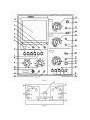
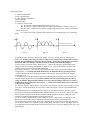
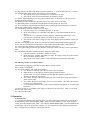
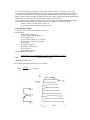
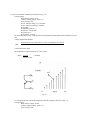
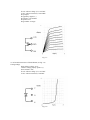
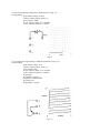
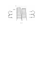
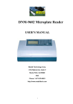
CA4810A Curve Tracer User’s Manual Madell Technology Corporation http://www.madelltech.com Copyright © 2005 CA4810A curve tracer is an instrument which can be used to view transistor and diode feature curves. It can also be used to measure their low frequency static-state characters, as well as other semiconductor and circuit measurements. 1. Specifications: 1.1 Vertical Axis Deflection Collector voltage (Ic): 2µA/DIV~1A/DIV, 15 steps, accuracy ± 3% Reversal drain current (IR): 0.2 µA/DIV~1A/DIV, 6 steps Accuracy: 2µA/DIV~10uA/DIV, ±3& 0.2µA/DIV~1uA/DIV, ±10% 0.2µA/DIV, interfere < 0.5V/DIV Base current or base voltage: 20mV/DIV, accuracy ±3% Deflection multiplying factor: x 0.5, accuracy ±10% 1.2 Horizontal Axis Deflection Collector Voltage: 0.05V/DIV~50V/DIV, 10 steps, accuracy ±3% Drain current voltage: 100V/DIV~550V/DIV, 3 steps, accuracy ±5% (with 5kV test fixture) Base voltage: 0.05V/DIV~2V/DIV, 6 steps, accuracy ±3%. 1.3 Step Signals Step current: 1µA~0.1A, 16 steps, accuracy ±5% Step voltage: 0.05V~2V, 6 steps, accuracy ±5% Stage Number per cluster: 4~10, continuously adjustable step zeroing: ≥ ±1DIV Stage Number per second: 200 Step Polarity: positive or negative Step mode: Continuous or single cluster 1.4 Collector Sweeping Supply Max. sweeping current: 0~5V: 10A 0~20V: 2.5A 0~100V: 0.5A 0~500V: 0.1A Dissipation Resistance: 0~500KΩ, 11 steps 10Ω~500kΩ, accuracy±10% 0.5Ω~2.5Ω, accuracy ±20% 1.5 Physical Desk top Dimension: 510 x 251 x 341mm Weight: 13.5kg Supply voltage: 110V±10%, 60Hz±5% Hz Apparent power: non-testing status: 50VA Max. power: 110VA 2. Switches The front panel is shown in figure 2.1, test fixture in figure 2.2 and back panel in figure 2.3. Fig. 2.1 Fig. 2.2 CA4810A front panel Front panel controls: (1) CRT focus adjustment. (2) Trace tilt adjustment. (3) CRT brightness adjustment. (4)Power on LED. (5) Power switch. (6) Collector AC/DC switch: AC: the collector is applied with alternate voltage (see fig. 2.3); DC: the collector is applied with DC pulsating voltage, rectified but not filtered (see fig. 2.4); DC and “I/DIV” switch at IR, the collector is applied with continuous DC voltage, rectified and filtered (see fig. 2.5); AC voltage can be used to show the forward and reverse C-V characteristic curves for bilateral diode. Fig. 2.3 Fig. 2.4 Fig. 2.5 (7) Max Peak Volts: maximum collector peak voltages: in 4 steps: 5V10A, 20V2.5A, 100V0.5A and 500V0.01A. Warning: when the peak collector voltage is to be changed, the Variable Collector knob (9) must first be anticlockwise returned to the “0” position. Set it to the required voltage percentage afterwards. Otherwise damages to the measured device and this instrument may happen. (8) INV: polarity of collector voltage. When it is at” +” position, the collector is applied with positive voltage, suitable for measuring NPN transistors; When it is at” –“position, the collector is applied with negative voltage, suitable for measuring PNP transistors. (9) Variable Collector %: collector peak voltage adjustment. This works in combination with the peak voltage buttons (7). Generally, this knob should always be adjusted from zero percentage and up. (10) Series Resistors Ω: these are dissipation limit resistors and are connected serially in the collector measurement loop. (11) Collector fuse: when the collector supply exceeds the rated power, this fuse will be blown off. The collector voltage output will be cut off. Caution: small triodes can be easily damaged if the collector voltage is suddenly changed to 500V, and the curve tracer may be damaged. Therefore, a 1A fuse is installed when the instrument leaves the factory. A 2A fuse can be used in place when it is necessary to measure large triodes. (12) Looping: capacitive current balance. The capacitive current produced by the collector supply can cause errors at low current measurement. It is necessary to reduce the capacitive current to the minimum before testing. (13) Compensation: this, in combination with Looping (12), will further reduce the capacitive current. (14) Series resistance: when the STEP/OFFSET AMPL(18) switch is set to one of the voltages, the voltage will be applied to the grid of the field effect transistor through the series resistance. Change the series resistance to match the input impedance of the measured device. (15) Press: when the “Repeat/Single Cluster” switch (16) is set to single cluster, press this button will display a new cluster. This feature is helpful for measuring outputs of heavy current transistors. (16) “Repeat/Single Cluster” switch: When it is at Repeat position, clusters will be continuously refreshed; Use the “Press” button(15) to refresh the cluster at single mode. The SGL led will be on at Single mode. It is recommended to use the single mode to measure heavy duty devices to prevent damages to the device and the instrument. (17) Step polarity switch: the step output is at positive polarity at “+” position and negative at “-“ position. (18) STEP/OFFSET AMPL switch: this switch serves two functions: a. Base current source from 1µA/STAGE to 0.1A/STAGE, in 16 steps. b. Base voltage source from 0.05V/STAGE to 2V/STAGE, in 6 steps. (19) Offset: Adjust this knob to cover any position between stages. It should be set at the zero level to measure amplifying multiples. (20) Number of steps: continuously adjust the step of every cluster from 4 to 10 stages, (21) Horizontal position: to adjust the horizontal position of the light trace on the screen. (22) Trace separation: adjust the horizontal display position of the right side measured device on the test fixture when “double cluster” test fixture is used. (23) VOLTS/DIV switch: this switch covers four ranges. a. Collector voltage (Vce): 0.05V/DIV~50V/DIV, in 10 steps b. Drain current voltage (VR): 100V/DIV~500V/DIV, in 3 steps (this matches the 5kV test fixture) c. Base voltage (VBE): 0.05V/DIV~2V/DIV, in 6 steps; when the step switch (18) is set at potential source position, the CRT X axis will show the step voltages. d. Base current or base source voltage: the CRT X axis displays the stage number of the step at this mode. (24) INV: reversal phase switch. When it is pressed down, both the vertical and horizontal signals will reverse 180°. It is convenient to use this feature to test a PNP transistor after testing a NPN transistor. (25) Vertical position: adjust the vertical position of the trace on the screen. (26) X0.5 switch: when pressed down, the deflection coefficient of I/DIV switch(27) will be expanded two times. (27) Current/DIV switch: this switch covers three deflection current ranges. a. Collector current (Ic): 20µA/DIV~1A/DIV, in 15 steps b. Drain current (IR): 10µ/DIV~0.2uA/DIV, in 6 steps. This range can only be used to measure the reversal drain current of diodes. c. Base current or base source voltage: Y axis will display the stage number at this mode. The following switches are on the test fixture. (28/30) Diode test plugholes: to test the reversal breakdown current of diodes. (29/31) Triodes test plugholes. (32) Test fixture settings: with 5 push down switches. a. Left: the device on the left side of the test fixture will be measured. b. Right: the device on the right side of the test fixture will be measured. c. Double cluster: the devices on both the left and right sides of the test fixture will be alternatively displayed on the screen. d. Zero current: the base of the measured transistor will be in the open-circuit status and the ICEO feature will be tested. e. Zero voltage: the base of the measured device is at zero potential. This mode can be used to test the IDSS of a FET transistor. f. (33) Conjugation switch for FET: it can be used to match the conjugations of two small FET transistors. (34) Power socket: AC~110V/60Hz power supply, on the back of the curve tracer. There is a 1A fuse at the lower part of the socket. (35) CRT color filter glass. 3. Operation 3.1 Introduction 3.1.1 Damages may happen to the measured device if switches on the front panel are not set properly. It is recommended to set the “STEP/OFFSET AMPL” switch (18) at the smallest level, the “Series resistance” switch (14) at the maximum value (100kΩ), the collector “SERIES RESISTORS” (10) at the maximum also, set Max Peak Volts to 5V, and Variable Collector % to zero. Adjust them to the required positions one by one according to the test conditions of the measured device. 3.1.2 When measuring power transistors, set the step at “Single” position. Increase the collector peak voltage, decrease the dissipation limit resistance or increase the step current to find the proper test values. 3.1.3 When measuring the reversal voltage, maximum dissipation limit resistance must be used (500kΩ or 1000kΩ); Set the collector current to IR, and increase the peak voltage slowly to reach the breakdown point; The IR feature is a continuous curve at AC mode, and it is a point at DC mode. 3.1.4 The double cluster function is mainly used to test the conjugation of current amplification multiples. For the safety of the measured devices, double cluster is not available at the following settings: Collector voltage is at 100V 0.5A or 500V 0.1A Step current is between 10mA/stage and 0.1A/stage 3.2 Measurement Examples 3.2.1 Output curves of NPN 9013 transistor (see Fig. 3-1) Testing settings: Peak collector voltage: 0~5V Collector voltage polarity: positive (+) Series resistors: 250Ω X axis: collector voltage (Vce): 0.5V/DIV Y axis: collector current (Ic): 1mA/DIV Step: Repeat Step polarity: positive (+) Step choice: 10µA/STAGE Step offset: zero Stage number: 10 stages Voltage amplification multiple: HFE = shown division of nth horizontal line on Y axis x Current/DIV (27) value Ic n x step switch (18) value n counts from bottom to top. The amplification computed from the 5th curve will be: HFE= 4 x 1mA = 160 times 5x(5x103)mA Fig. 3-1 3.2.2 HFE measurement of NPN 9013 transistor (see Fig. 3-2) Testing settings: Peak collector voltage: 0~5V Collector voltage polarity: positive (+) Series resistors: 250Ω X axis: collector voltage (Vce): 0.5V/DIV Y axis: collector current (Ic): 1mA/DIV Step: Repeat Step polarity: positive (+) Step choice: 5µA/STAGE Step offset: zero Stage number: 10 stages The following curves in Fig. 3-2 are obtained by turning the X axis horizontal switch anticlockwise to the end. Voltage amplification multiple: HFE = shown division of nth vertical line on Y axis x Current/DIV (27) value Ic n x step switch (18) value n counts from left to right. The amplification computed from the 10th curve will be: HFE= 8 x 1mA 10x(5x103)mA = 160 times Fig. 3-2 3.2.3 Output characters of N Channel-depletion field effect transistor 3DJ7G (see Fig. 3-3) Testing settings: Peak collector voltage: 0~20V Collector voltage polarity: positive (+) Series resistors: 250Ω X axis: collector voltage (Vce): 0.5V/DIV Y axis: collector current (Ic): 0.5mA/DIV Step: Repeat Step polarity: negative (-) Step choice: 0.2V/STAGE Step offset: zero Stage number: 10 stages Fig. 3-3 3.2.4 Forward current curve of diode IN4148 (see Fig. 3-4) Testing settings: Peak collector voltage: 0~5V Collector voltage polarity: positive (+) Series resistors: 250Ω X axis: collector voltage (Vce): 0.1V/DIV Y axis: collector current (Ic): 1mA/DIV Fig. 3-4 3.2.5 Reversal breakdown voltage test of diode IN4148 (see Fig. 3-5) Testing settings: Peak collector voltage: 0~500V Collector voltage polarity: positive (+) Series resistors: 100KΩ X axis: collector voltage (Vce): 20V/DIV Y axis: collector current (Ic): 1µA/DIV Fig.3-5 3.2.6 Common base output feature of NPN 9013 transistor (see Fig. 3-6) Testing settings: Peak collector voltage: 0~5V Collector voltage polarity: positive (+) Series resistors: 250Ω X axis: collector voltage (Vce): 0.5V/DIV Y axis: collector current (Ic): 1mA/DIV Step: Repeat Step polarity: negative (-) Step choice: 0.1mA/STAGE Step offset: zero Stage number: 10 stages Fig. 3-6 3.2.7 Double cluster display of NPN 9013 transistor output features (see Fig. 3-7) Testing settings: Peak collector voltage: 0~5V Collector voltage polarity: positive (+) Series resistors: 250Ω X axis: collector voltage (Vce): 1V/DIV Y axis: collector current (Ic): 1mA/DIV Step: Repeat Step polarity: positive (+) Step choice: 5µA/STAGE Step offset: zero Stage number: 10 stages Double cluster selected on the test fixture. Fig.3-7 Note: the trace separation knob (22) can be used to move the two clusters closer for better observations. 3.2.8 Switching character of high cut-in voltage VMOS transistor IRF840 (see Fig. 3-8) Testing settings: Peak collector voltage: 0~20V Collector voltage polarity: positive (+) Series resistors: 250Ω X axis: collector voltage (Vce): 0.5V/DIV Y axis: collector current (Ic): 1mA/DIV Step: Repeat Step polarity: negative (-) Step choice: 0.5V/STAGE Step offset: zero Stage number: 4 stages Double cluster selected on the test fixture. Fig. 3-4