1
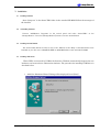
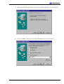
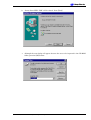
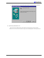
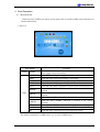
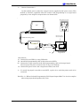
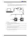
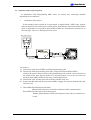
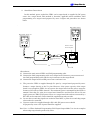
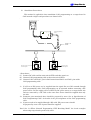
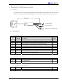
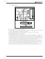
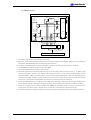
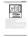
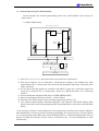
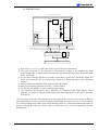
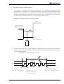
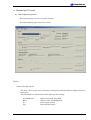
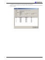
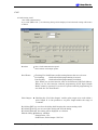
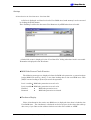
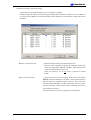
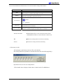
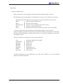
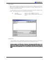
CAN
Flash Microcomputer
Programmer
S810-CFW1
Operation Manual
Sunny Giken Inc.
Sunny Giken Inc.
This operation manual is described in accordance with the S810-CFW1 Ver1.10.
CAN Flash Microcomputer Programmer
S810-CFW1
Contents of this manual may be revised without notice.
We, Sunny Giken Inc. shall not be responsible for any damages and/or losses
caused by using this product and/or the software attached to this product claimed by
users and/or any intermediaries.
Specifications of this product and/or the software attached to this product may be
modified without notice due to product improvements.
Names of systems, products, and/or services used in this manual are either
registered trademarks or trademarks of each manufacturer.
In addition, captions of the TM and (R) are not mentioned in this manual.
S810-CFW1, CAN Flash Microcomputer Programmer Operation Manual
1
Sunny Giken Inc.
1 Outline .....................................................................................................................................................................3
1.1 Precautions ......................................................................................................................................................3
1.2 System Configuration .....................................................................................................................................4
2 Specifications...........................................................................................................................................................5
2.1 General Specifications ....................................................................................................................................5
2.2 Power Supply Specifications ..........................................................................................................................5
2.3 Function Specifications...................................................................................................................................6
2.4 Programmable Devices...................................................................................................................................6
3 Installation ..............................................................................................................................................................7
3.1 Installing Software..........................................................................................................................................7
3.2 Uninstalling Software.....................................................................................................................................7
3.3 Installing Acrobat Reader...............................................................................................................................7
3.4 Installing USB Driver.....................................................................................................................................7
3.5 Disconnecting USB Cable from a PC..........................................................................................................10
4 Panel Description ................................................................................................................................................. 11
4.1 S810-CFW1 Unit........................................................................................................................................... 11
5 Instructions for Connection and Standalone Operation ..................................................................................13
5.1 PC Remote CAN Programming Mode ........................................................................................................14
5.2 Standalone CAN Programming Mode ........................................................................................................17
6 Specifications of CAN Programming Cable.......................................................................................................20
6.1 Connector .......................................................................................................................................................20
6.2 Pin Assignment..............................................................................................................................................20
7 Connection Circuit Example ...............................................................................................................................21
7.1 Onboard Programming (CAN Input Output Mode)..................................................................................21
7.2 Network Programming (CPU Rewriting Mode) ........................................................................................27
7.3 Connecting a Probe for a Watch-dog Timer................................................................................................29
8 Operation by PC Control .....................................................................................................................................30
8.1 Main Programming Screens ........................................................................................................................30
8.2 Menu Bar .......................................................................................................................................................38
8.2.1 Project Menu.................................................................................................................................................38
8.2.2 Edit Menu......................................................................................................................................................39
8.2.3 Help Menu.....................................................................................................................................................42
8.3 Error Messages..............................................................................................................................................43
9 List of LED Status................................................................................................................................................45
10 Updating Firmware ...........................................................................................................................................46
S810-CFW1, CAN Flash Microcomputer Programmer Operation Manual
2
Sunny Giken Inc.
1 Outline
1.1 Precautions
Thank you for purchasing our product S810-CFW1, the CAN Flash Microcomputer
Programmer.
Please read this operation manual carefully to understand the function of this product for
effective and stable operation. Please beware that Sunny Giken Inc. shall have no liability for
any damage and/or troubles caused by misuse or careless handling.
1) General Caution
Please follow the precautions mentioned below to avoid hazards such as fire, burns, electric
shock, and/or injures.
● Make sure that the power switch of this product is turned OFF and your hands are clean and
dry when an AC adapter is plugged in.
● Use this product under proper environment.
● Never place this product up-side-down or lateral side facing to table.
● Handle this product with care to avoid fall and/or physical shock.
● Never take this product apart and/or modify by yourself.
2) Operating Environmental Condition
● Unusable environment
Dusty place
Place in the presence of corrosive gasses
Place exposed to direct sunlight
Place surrounded by noise source equipment
Place with severe mechanical shock and/or constant mechanical vibration
● Ambient temperature 0°C to +40°C Humidity : below 80% (non condensing)
● Prevention of electrostatic is recommended in operating this product and devices.
3) Storage
● Place this product into the packing box in which the product was delivered when you
purchased. Store it at shaded place with the ambient temperature of -10°C to +40°C and
below 80% of humidity (non condensing) for long term storage.
4) Transportation
● In case the product is needed to be relocated, use the packing box in which the product was
delivered when you purchased.
5) Cleaning
● Wipe the product with soft and clean fabric. Do not use any sort of organic solvent such as
benzine that may cause deterioration of this product.
S810-CFW1, CAN Flash Microcomputer Programmer Operation Manual
3
Sunny Giken Inc.
1.2 System Configuration
The entire system configuration of the CAN Flash Microcomputer Programmer (hereinafter called
“CFW1”) is illustrated below.
CD-ROM
Control Program
Operation Manual
Others
PC
Renesas CAN
microcomputer
USB connecting cable
DC cable
CAN programming
cable
User prepared
target board
* AC adapter is not included as part of the product.
* See “5. Setting Up” for details of connection.
S810-CFW1, CAN Flash Microcomputer Programmer Operation Manual
4
Sunny Giken Inc.
2 Specifications
2.1 General Specifications
Main unit of the CFW1
Ambient temperature: 0°C to 40°C
Operating
Humidity: below 80% (non condensing)
environment
Storage
Ambient temperature: -10°C to +40°C
environment
External
Approximately 85 (W) x 60.5 (D) x 18 (H) mm (Projection not included)
dimensions
Weight
Approximately 75g (only the main unit)
2.2 Power Supply Specifications
Using DC Cable
Power supply
DC +12V
Power
consumption
200mA maximum, 50mA average
The polarity of this DC cable is illustrated below.
500mm
Wire color
RED:DC+12V
BLACK:GND
Using CAN Cable
Power supply
DC +5V ±5%
Power
consumption
300mA maximum, 100mA average
Using USB Cable
Power supply
DC +5V ±5%
Power
consumption
500mA maximum, 100mA average
* DC +5V±5%, maximum of 500mA of power supply is needed to start CFW1. When
using USB cable, use PC or USB hub that bears minimum of 4.75V, 500mA of
power supply.
S810-CFW1, CAN Flash Microcomputer Programmer Operation Manual
5
Sunny Giken Inc.
2.3 Function Specifications
Programmable
MCU
Operation Mode
Program Mode
Renesas CAN Microcomputers
See “cfw1deve.pdf” in the attached CD-ROM.
CAN programming mode
PC remote CAN programming
Standalone CAN programming
PC control
Software
All the operation can be achieved from your PC with easy-to-operate
GUI(Graphic User Interface). Applicable to Windows98/2000/Me/XP.
Interface
USB (Full Speed: 12Mbps)
2.4 Programmable Devices
Programmable devices are the Renesas CAN Microcomputers. Some of the devices are, however,
still under evaluation or not yet programmable. Refer to the attached file “Programmable Device
List” in the attached CD-ROM.
For the latest information, contact Sunny Giken Inc..
S810-CFW1, CAN Flash Microcomputer Programmer Operation Manual
6
Sunny Giken Inc.
3 Installation
3.1 Installing Software
Start “Setup.exe” in the S810-CFW1 folder in the attached CD-ROM. Follow the messages of
the installer.
3.2 Uninstalling Software
Execute “Add/Remove Programs” in the control panel and select “S810-CFW1” in the
“Change/Remove”. Press the [Change/Remove] button to execute uninstallation.
3.3 Installing Acrobat Reader
You need Acrobat Reader in order to refer to the “Manual” of the “Help”. If Acrobat Reader is not
installed on your PC, start “AR405ENG.EXE” in ACROBAT folder in the attached CD-ROM.
3.4 Installing USB Driver
When CFW1 is connected by USB for the first time, Windows automatically inspects the new
hardware and creates driver information database. The procedure for installing USB Driver is
described below:
i. “Add New Hardware Wizard” Dialog will be displayed. Press [Next].
S810-CFW1, CAN Flash Microcomputer Programmer Operation Manual
7
Sunny Giken Inc.
ii. Select “Search for the best driver for your device. (Recommended)” and press [Next]
iii. Specify “USBDrv” folder in the attached CD-ROM for areas to be inspected.
S810-CFW1, CAN Flash Microcomputer Programmer Operation Manual
8
Sunny Giken Inc.
iv. “Sunny S810-CFW1 USB” will be viewed. Press [Next].
v. Although the next dialog will appear because the area to be inspected is the CD-ROM
folder, press the [OK] button.
S810-CFW1, CAN Flash Microcomputer Programmer Operation Manual
9
Sunny Giken Inc.
vi. The driver files will be automatically copied and then, installation will be completed.
3.5 Disconnecting USB Cable from a PC
Do not disconnect USB cable from a PC while the control program is being activated.
USB cable can be disconnected anytime as long as the control program is not being activated.
S810-CFW1, CAN Flash Microcomputer Programmer Operation Manual
10
Sunny Giken Inc.
4 Panel Description
4.1 S810-CFW1 Unit
External views of CFW1 are shown and its parts such as switches, LEDs, and connectors are
also described below.
• Top view
Switch/LED
Switch
POWER
Executes command responding to LED which is turned on when the
power supply switch is turned on.
Turns ON when the power supply switch is turned on.
PASS
Turns ON when CAN programming is successful.
ID ERR
Turns ON when result of CAN programming is ID_ERR.
FAIL
Turns ON when CAN programming is failed.
E/P/V
READ
Turns ON when E/P/V command is selected in the control program.
Turns ON when BLANK command is selected in the control
program.
Turns ON when ERASE command is selected in the control
program.
Turns ON when E/P/ command is selected in the control program.
Turns ON when VERIFY command is selected in the control
program.
Turns ON when READ command is selected in the control program.
Tx
Turns ON when CAN frame is sent from CFW1.
Rx
Turns ON when CAN frame is received from the target.
START
BLANK
LED
Function
ERASE
E/P
VERIFY
For further information on LED status, see “10. List of LED Status”.
S810-CFW1, CAN Flash Microcomputer Programmer Operation Manual
11
Sunny Giken Inc.
● Right-hand side view
Connector
TARGET
Function
Connector for CAN programming cable
● Left-hand side view
USB
DC IN
Connector
Function
USB
Connector for USB cable (mini-B Plug)
DC IN
Connector for DC cable.
S810-CFW1, CAN Flash Microcomputer Programmer Operation Manual
12
Sunny Giken Inc.
5 Instructions for Connection and Standalone Operation
Connection instructions are illustrated below.
There are mainly two types of connection.
-PC Remote CAN Programming Mode
Connecting PC to CFW1 with USB enables CFW1 to achieve PC Remote CAN Programming
Mode. CAN programming is executed by using CFW1 control program in PC Remote CAN
Programming Mode. For directions for using CFW1 control program, see “8. Operation by PC
Control Program”.
-Standalone CAN Programming Mode
Using CFW1 alone without connecting PC to CFW1 enables it to achieve Standalone CAN
Programming Mode. The main unit of CFW1 can automatically save set conditions and data
by control program. Therefore, CFW1 can achieve CAN programming by itself as long as there
is no change in the data. Pressing START switch will complete the operation. Since advanced
setting is not necessary, it is easy to program.
In addition, LED of the main unit of CFW1 indicates set execution state.
For further information on the control program, see “8. Operation by PC Control Program”.
<Instructions for Data Setting>
(1) Connect PC to CFW1 by using USB cable and start PC control program.
(2) Select MCU name and set baudrate and others.
(3) Load data for programming
(4) Set lockbits and pulse output if necessary.
(5) Check command you would like to execute. (Erase/Program/Verify, Blank, and others)
(6) Select “Project”, then “Exit” in the menu bar and close the control program
PC
USB C on necting cable
PA SS
I DE RR
FAI L
E/P/V
BLA NK
ERA SE
E/P
VER F
IY
REA D
US B
PO WER
TX
DC I N
TAR GET
RX
STA RT
<Instructions for CAN Programming>
(1) Connect CFW1 to a target board by following the optimum way for the target board and
turn it on.
(2) Press START switch to execute processing which is selected in Action.*1
(3) When the processing is completed, LED of the main unit will output the result.
(4) Turn it off and disconnect the CFW1 from the target board.
Start from the first step every time if you would like to repeat the operation.
*1 When loading programming data from internal memory, contents of the memory are checked whether they
are kept safely (Checksum check). If not, FAIL LED will flash. If this happens, press START switch to stop
LED flashing. Then, reload the data after formatting the main unit of the CFW1 by using CFW1 control
program.
S810-CFW1, CAN Flash Microcomputer Programmer Operation Manual
13
Sunny Giken Inc.
5.1 PC Remote CAN Programming Mode
In PC Remote CAN Programming Mode, there are mainly three connecting methods depending
on the conditions.
i.
Remote Connection 1
In this method, power needed for a target board is supplied from a CFW1 side. A figure
and procedures for the connection are shown below. Note that the connection method shown
below is applicable to our products, S810-CHX3, CHX4. See “Remote Connection 2” in the
next page, if you use a board produced by users.
PC
USB connecting cable
CAN programming cable
S810-CHX3, CHX4... *1
<Procedures>
(1) Connect PC and CFW1 by using USB cable.
(2) Attach CAN programming cable to the main unit of CFW1.
(3) Connect CAN programming cable and a target board (S810-CHX3, CHX4). Connect the
power connector of the CAN programming cable and 10 pin connector to the target board.
Note that a probe for a watch dog timer is not to be used since our products, S810-CHX3,
CHX4, have no watch dog timer function.
*1
S810-CHX3: Evaluation board for CAN
Mounted with CAN transceiver to enable evaluation of CAN communication.
S810-CHX4: IC socket type CAN writing board
Enables programming flash micro-computers before they are mounted in the
board.
S810-CFW1, CAN Flash Microcomputer Programmer Operation Manual
14
Sunny Giken Inc.
ii.
Remote Connection 2
In this method, power needed for a target board is supplied by DC power source. This
method is, therefore, applicable when PC remote CAN programming on a target board
prepared by users. A figure and procedures are shown below.
DC power source
PC
Renesas CAN
microco mput er
USB connecti ng ca ble
CA N prog rammin g
cable
*1
Us er prepared
target board
<Procedures>
(1) Connect PC and CFW1 by using USB cable.
(2) Attach CAN programming cable to the main unit of CFW1.
(3) Connect the 10 pin connector of the CAN programming cable to the target board.
Do not connect the power connector since it may cause damage.
(4) Connect DC power source and a target board. Then, turn it on.
*1: If a watch dog signal is needed to start MCU, a probe for a watch dog timer needs to be
connected.
Note)See “7.1 When On-board Programming (CAN Input Output Mode)” for circuit examples
when using target boards produced by users.
S810-CFW1, CAN Flash Microcomputer Programmer Operation Manual
15
Sunny Giken Inc.
iii. Remote Connection 3
In this method, power needed for a target board is supplied by power source in
network. This method, therefore, is applicable when PC remote programming on target
boards in CAN network. A figure and procedures are shown below.
CA N
pro grammin g
cable
U S B con n ec ti ng ca b le
PC
CAN + *1
CAN -
*2
Renesas CAN
microco mput er
Renesas CAN
microco mputer
Us er prepared target bo ard
Us er prepared target bo ard
<Procedures>
(1) Connect PC and CFW1 by using USB cable.
(2) Attach CAN programming cable to the main unit of CFW1.
(3) Connect CAN+ and CAN- in CAN network and CAN+ and CAN- pins of CAN
programming cable.
*1: Connector pins should be prepared by users. See “6.Specifications of CAN Programming
Cable” for pin assignment of CAN programming cable.
*2: This method provides that CAN network is turned on. If it is not turned on, turn it on first,
and then follow the procedures described above.
Note) See “7.2 When Network Programming (CPU Rewriting Mode)” for circuit examples
when using target boards produced by users.
S810-CFW1, CAN Flash Microcomputer Programmer Operation Manual
16
Sunny Giken Inc.
5.2 Standalone CAN Programming Mode
In Standalone CAN Programming Mode, there are mainly four connecting methods
depending on the conditions.
i.
Standalone Connection 1
In this method, power needed for a target board is supplied from a CFW1 side. A figure
and procedures for the connection are shown below. Note that the connection method shown
below is applicable to our products, S810-CHX3, CHX4. See “Standalone Connection 2” in
the next page, if you use a board produced by users.
DC power source
PA SS
I DE RR
FAI L
E/P/V
BLA NK
ERA SE
E/P
VER F
IY
REA D
US B
PO WER
TX
DC I N
DC cable
TAR GET
RX
STA RT
CAN programming
cable
S810-CHX3,CHX4....*1
<Procedures>
(1) Connect the main unit of CFW1 and CAN programming cable.
(2) Connect the CAN programming cable and a target board (S810-CHX3, CHX4).
Connect the power connector of the CAN programming cable and the 10 pin connector to
the target board. Note that the probe for a watch-dog timer is not to be used since our
products, S810-CHX3, CHX4, do not have a watch-dog function.
(3) Connect DC cable and the main unit of CFW1 and then turn it on.
(4) Connect the DC cable and the main unit of CFW1. Supply 12V of power from the DC cable
and turn it on.
*1
S810-CHX3: Evaluation board for CAN
Mounts CAN transceiver to enable evaluation of CAN communication.
S810-CHX4: IC socket type CAN writing board
Enables programming a flash microcomputer before that is mounted on a
board.
S810-CFW1, CAN Flash Microcomputer Programmer Operation Manual
17
Sunny Giken Inc.
ii. Standalone Connection 2
In this method, power needed for CFW1 and a target board is supplied by DC power
source for a target board. This method is, therefore, applicable when standalone CAN
programming on a target board prepared by users. A figure and procedures are shown
below.
DC power source
DC power sour ce *3
Renesas CAN
microco mput er
DC cable
CA N programmin g
cable
*1
Us er prepare d
t arge t board
*2
<Procedures>
(1) Connect the main unit of CFW1 and CAN programming cable.
(2) Connect the CAN programming cable and a target board. Connect a power connector of
the CAN programming cable and the 10 pin connector to the target board.
(3) Connect the target board and DC power source and turn it on.
*1: The power for CFW1 is supplied through Vcc pins by a target board prepared by users.
Connect a target directly to the Vcc pins. However, if the power capacity of the target
board is not enough for CFW1, do not connect the target board and the power connector.
Connect a DC cable to CFW1 instead. ( The maximum power consumption of the CFW1 is
300mA.) Note that Vcc pins for a target board should be used between 5V±5%. Do not
supply power to CFW1 by DC power source on a target board side and one connected by a
DC cable at the same time. Power should be supplied from only one side.
*2: In case that a watch-dog signals are needed to start MCU, a probe for a watch-dog output
also needs to be connected.
*3: If power needs to be supplied through a DC cable, DC power source should
be prepared by users. 12V of power should be supplied.
Note) See “7.1 When Onboard Programming (CAN Input Output Mode)” for circuit examples
when using target boards produced by users.
S810-CFW1, CAN Flash Microcomputer Programmer Operation Manual
18
Sunny Giken Inc.
iii. Standalone Connection 3
This method is applicable when standalone CAN programming on a target board in
CAN network. A figure and procedures are shown below.
D C p ower sour ce * 3
CAN programming
cable
DC ca ble
CAN + *2
CAN -
*1
Renesas CAN
microco mputer
Renesas CAN
microco mputer
Us er p rep ar e d ta rg e t b oa rd
Us er p rep ar ed t a rg e t b o a rd
<Procedures>
(1) Connect DC cable and the main unit of CFW1 and then turn it on.
(2) Connect CAN programming cable to the main unit of CFW1.
(3) Connect CAN+ and CAN− pins in CAN network and CAN+ and CAN− pins of the
CAN programming cable.
*1: If ±5V±5% of DC power can be supplied from the signal line on CAN network through
CAN programming cable, CAN programming can be operated without connecting a DC
power source. Do not supply power to CFW1 by DC power source on a target board side
and one connected by a DC cable at the same time. Power should be supplied from only
one side.
*2: Connector pins mentioned above should be prepared by users. See “6. Specifications of
CAN Programming Cable” for details of the pin assignment of the CAN programming
cable.
*3: If power needs to be supplied through a DC cable, DC power source should
be prepared by users. 12V of power should be supplied.
Note) See “7.2 When Network Programming (CPU Rewriting Mode)” for circuit examples
when using target boards produced by users.
S810-CFW1, CAN Flash Microcomputer Programmer Operation Manual
19
Sunny Giken Inc.
6 Specifications of CAN Programming Cable
6.1 Connector
An external view of the CAN programming cable (S810-CFW1) is shown below. Note that this cable
is ISO11898 compliant.See”6.2 Pin Assignment” for details of pin assignment for each connector.
9
10
1
2
HR S
HRS
500mm
12
JST
12
C
10 pin connector
Power connector
Probe for a watch-dog timer
6.2 Pin Assignment
(1) 10 pin connector
Pin No.
Signal Name
Description
Direction
1
Vcc MON
Vcc Monitor
2
SEL1
SEL1 signal output for CAN programming
Input
Output
3
SEL2
SEL2 signal output for CAN programming
Output
4
CAN-
Receiving frame signal input for CAN programming
5
CE*
CE signal output for CAN programming
Output
6
EPM*
EPM signal output for CAN programming
Output
7
GND
Signal ground
8
RESET*
RESET signal output for CAN programming
Output
9
CNVss
CNVss (Vpp) signal output for CAN programming
Output
10
CAN+
Send frame for CAN programming
-
-
-
(2) Power connector
Pin No.
1
2
Signal Name
Vcc
Description
Vcc Input Output
GND
Signal ground
*The direction can be different depending on a connection method.
Direction
*
-
(3) Probe for a watch-dog timer
Pin No.
-
Signal Name
WDT
Description
Pulse signal output for a watch-dog timer
Direction
Output
* The input output level for the CAN programming cable should be between 5V±5%.
S810-CFW1, CAN Flash Microcomputer Programmer Operation Manual
20
Sunny Giken Inc.
7 Connection Circuit Example
7.1 Onboard Programming (CAN Input Output Mode)
Circuit examples for onboard programming under user oriented MCU circuit design are
shown below:
(1) M16C/6NA,6NB
User Prepared Target Board
CAN+
MCU
Peripheral
Circuit
*4
*9
CAN
Driver
*5
MCU
CTx
Vcc
CRx
CANNMI
*6
CE
EPM
Reset Circuit
*7
CNVss
Vss
Reset
*8
1
2
1
2
3 4 5 6 7 8
9 10
3 4 5 6 7 8
9 10
*2
GND CNVss
Vcc
*1
Vcc
SEL2
CE*
SEL1 CAN-
EPM* RESET CAN+
*3
WDT
GND
CFW1 Unit
*1.
Leave No.2 and 3 pins of the 10 pin connectors unconnected.
*2. The power connector can be connected or unconnected according to the conditions for CAN programming. (See “5. Instructions
for Connection and Standalone Operation” for details of the power connector.)
*3. In case that watch-dog signals are needed to start the MCU, a probe for a watch-dog output also needs to be connected.
*4. Connect ISO11898 compliant CAN driver to CTx and CRx of MCU.
*5. Attach a terminating resistance to CAN+,− of the CAN bus.
*6. Isolate CE and EPM pins from the MCU peripheral circuit, in case the jumper, analog switch, three state, etc. are built in, when
onboard programming. Isolation can be omitted when those signal statuses are output from the MCU peripheral circuit.
Resistance should be 4.7KΩ or over when pull-up is achieved to these signals. When pull-up is achieved to CE pin, and pull-down
is achieved to EPM pin, no connection to CE and EPM of CFW1 is required and the isolation alone can be conducted. In case that
these pins are not being used in the circuit, it is also possible to fix CE and EPM pins to H and L levels directly on the board
respectively.
*7. Connect the MCU CNVss pin to the CNVss pin of the CFW1 unit by achieving “pull up/down” with resistance of 10KΩ. In case
that it is defined to H level by switching the jumper of the CNVss pin, no connection to the CNVss pin of CFW1 is not required.
*8. Connect the reset pin of the user target board MCU to the RESET pin of the CFW1 directly when the reset circuit of the user
target board is “open collector output”, “CR delay circuit”, or constant current load circuit is less than dozens of µA.
*9. See “Renesas Microcomputer Hardware Manuals” for details of onboard programming (CAN Input Output Mode) of each device.
S810-CFW1, CAN Flash Microcomputer Programmer Operation Manual
21
Sunny Giken Inc.
(2) M16C/6N4, 6N5, 6NK, 6NL, 6NM, 6NN group
User Prepared Target Board
CAN+
MCU
Peripheral
Circuit
*4
*9
CAN
Driver
*5
MCU
CTx
Vcc
CRx
CANTxD1
*6
CE
EPM
NMI
CLK1
Reset Circuit
*7
CNVss
Vss
Reset
*8
1
2
1
2
3 4 5 6 7 8
9 10
3 4 5 6 7 8
9 10
*2
GND CNVss
Vcc
*1
Vcc
SEL2
CE*
SEL1 CAN-
EPM* RESET CAN+
*3
WDT
GND
CFW1 Unit
*1. Leave No.2 and 3 pins of the 10 pin connectors unconnected.
*2. The power connector can be connected or unconnected according to the conditions for CAN programming. (See “5. Instructions for
Connection and Standalone Operation” for details of the power connector.)
*3. In case that watch-dog signals are needed to start the MCU, a probe for a watch-dog output also needs to be connected.
*4. Connect ISO11898 compliant CAN driver to CTx and CRx of MCU.
*5. Attach a terminating resistance to CAN+,− of the CAN bus.
*6. Isolate CE and EPM pins from the MCU peripheral circuit, in case the jumper, analog switch, three state, etc. are built in, when
onboard programming. Isolation can be omitted when those signal statuses are output from the MCU peripheral circuit.
Resistance should be 4.7KΩ or over when pull-up is achieved to these signals. When pull-up is achieved to CE pin, and pull-down
is achieved to EPM pin, no connection to CE and EPM of CFW1 is required and the isolation alone can be conducted. In case that
these pins are not being used in the circuit, it is also possible to fix CE and EPM pins to H and L levels directly on the board
respectively.
*7. Connect the MCU CNVss pin to the CNVss pin of the CFW1 unit by achieving “pull up/down” with resistance of 10KΩ. In case
that it is defined to H level by switching the jumper of the CNVss pin, no connection to the CNVss pin of CFW1 is not required.
*8. Connect the reset pin of the user target board MCU to the RESET pin of the CFW1 directly when the reset circuit of the user
target board is “open collector output”, “CR delay circuit”, or constant current load circuit is less than dozens of µA.
*9. See “Renesas Microcomputer Hardware Manuals” for details of onboard programming (CAN Input Output Mode) of each device.
S810-CFW1, CAN Flash Microcomputer Programmer Operation Manual
22
Sunny Giken Inc.
(3) M32C/84,85 group
User Prepared Target Board
CAN+
MCU
Peripheral
Circuit
*4
*9
*5
MCU
CTx
CAN
Driver
Vcc
CRx
CAN*6
CE
EPM
NMI
SCLK
Reset Circuit
*7
CNVss
Vss
Reset
*8
1
2
1
2
3 4 5 6 7 8
9 10
3 4 5 6 7 8
9 10
*2
GND CNVss
Vcc
*1
Vcc
SEL2
CE*
SEL1 CAN-
EPM* RESET CAN+
*3
WDT
GND
CFW1 Unit
*1. Leave No.2 and 3 pins of the 10 pin connectors unconnected.
*2. The power connector can be connected or unconnected according to the conditions for CAN programming. (See “5. Instructions for
Connection and Standalone Operation” for details of the power connector.)
*3. In case that a watch-dog signals are needed to start MCU, a probe for a watch-dog output also needs to be connected.
*4. Connect ISO11898 compliant CAN driver to CTx, CRx of MCU.
*5. Attach a terminating resistance to CAN+,− of the CAN bus.
*6. Isolate CE and EPM pins from the MCU peripheral circuit in case the jumper, analog switch, three state, etc. are built in, when
onboard programming. Isolation can be omitted when those signal statuses are output from the MCU peripheral circuit.
Resistance should be 4.7KΩ or over when pull-up is achieved to these signals. When pull-up is achieved to CE and EPM pins, no
connection to CE and EPM of CFW1 is required and the isolation alone can be conducted. In case that these pins are not being
used in the circuit, it is also possible to fix CE and EPM pins to H and L levels directly on the board respectively.
*7. Connect the MCU CNVss pin to the CNVss pin of the CFW1 unit by achieving “pull up/down” with resistance of 10KΩ. In case
that it is defined to H level by switching the jumper of the CNVss pin, no connection to the CNVss pin of CFW1 is not required.
*8. Connect the reset pin of the user target board MCU to the RESET pin of the CFW1 directly when the reset circuit of the user
target board is “open collector output”, “CR delay circuit”, or constant current load circuit is less than dozens of µA.
*9. See “Renesas Microcomputer Hardware Manuals” for details of onboard programming (CAN Input Output Mode) of each device.
S810-CFW1, CAN Flash Microcomputer Programmer Operation Manual
23
Sunny Giken Inc.
(4) M16C/1N group
User Prepared Target Board
CAN+
MCU
Peripheral
Circuit
*4
*9
*5
MCU
CTx
CAN
Driver
Vcc
CRx
CAN*6
CE
SEL
SCLK
Reset Circuit
*7
CNVss
Vss
Reset
*8
1
2
1
2
3 4 5 6 7 8
9 10
3 4 5 6 7 8
9 10
*2
GND CNVss
Vcc
*1
Vcc
SEL2
CE*
SEL1 CAN-
EPM* RESET CAN+
*3
WDT
GND
CFW1 Unit
*1. Leave No.3 and 6 pins of the 10 pin connectors unconnected.
*2. The power connector can be connected or unconnected according to the conditions for CAN programming. (See “5. Instructions for
Connection and Standalone Operation” for details of the power connector.)
*3. In case that a watch-dog signals are needed to start MCU, a probe for a watch-dog output also needs to be connected.
*4. Connect ISO11898 compliant CAN driver to CTx, CRx of MCU.
*5. Attach a terminating resistance to CAN+,− of the CAN bus.
*6. Isolate CE and SEL pins from the MCU peripheral circuit in case the jumper, analog switch, three state, etc. are built in, when
onboard programming. Isolation can be omitted when those signal statuses are output from the MCU peripheral circuit.
Resistance should be 4.7KΩ or over when pull-up is achieved to these signals. When pull-up is achieved to CE and SEL pins, no
connection to CE and SEL1 of CFW1 is required and the isolation alone can be conducted. In case that these pins are not being
used in the circuit, it is also possible to fix CE and SEL pins to H and L levels directly on the board respectively.
*7. Connect the MCU CNVss pin to the CNVss pin of the CFW1 unit by achieving “pull up/down” with resistance of 10KΩ. In case
that it is defined to H level by switching the jumper of the CNVss pin, no connection to the CNVss pin of CFW1 is not required.
*8. Connect the reset pin of the user target board MCU to the RESET pin of the CFW1 directly when the reset circuit of the user
target board is “open collector output”, “CR delay circuit”, or constant current load circuit is less than dozens of µA.
*9. See “Renesas Microcomputer Hardware Manuals” for details of onboard programming (CAN Input Output Mode) of each device.
S810-CFW1, CAN Flash Microcomputer Programmer Operation Manual
24
Sunny Giken Inc.
(5) M16C/29 group
User Prepared Target Board
CAN+
MCU
Peripheral
Circuit
*4
*9
*5
MCU
CTx
CAN
Driver
Vcc
CRx
CANTxD
*6
CE
RP
SCLK
Reset Circuit
*7
CNVss
Vss
Reset
*8
1
2
1
2
3 4 5 6 7 8
9 10
3 4 5 6 7 8
9 10
*2
GND CNVss
Vcc
*1
Vcc
SEL2
CE*
SEL1 CAN-
EPM* RESET CAN+
*3
WDT
GND
CFW1 Unit
*1. Leave No.2 and 3 pins of the 10 pin connectors unconnected.
*2. The power connector can be connected or unconnected according to the conditions for CAN programming. (See “5. Instructions for
Connection and Standalone Operation” for details of the power connector.)
*3. In case that a watch-dog signals are needed to start MCU, a probe for a watch-dog output also needs to be connected.
*4. Connect ISO11898 compliant CAN driver to CTx, CRx of MCU.
*5. Attach a terminating resistance to CAN+,− of the CAN bus.
*6. Isolate CE and RP pins from the MCU peripheral circuit in case the jumper, analog switch, three state, etc. are built in, when
onboard programming. Isolation can be omitted when those signal statuses are output from the MCU peripheral circuit.
Resistance should be 4.7KΩ or over when pull-up is achieved to these signals. When pull-up is achieved to CE and RP pins, no
connection to CE and RP of CFW1 is required and the isolation alone can be conducted. In case that these pins are not being used
in the circuit, it is also possible to fix CE and RP pins to H and L levels directly on the board respectively.
*7. Connect the MCU CNVss pin to the CNVss pin of the CFW1 unit by achieving “pull up/down” with resistance of 10KΩ. In case
that it is defined to H level by switching the jumper of the CNVss pin, no connection to the CNVss pin of CFW1 is not required.
*8. Connect the reset pin of the user target board MCU to the RESET pin of the CFW1 directly when the reset circuit of the user
target board is “open collector output”, “CR delay circuit”, or constant current load circuit is less than dozens of µA.
*9. See “Renesas Microcomputer Hardware Manuals” for details of onboard programming (CAN Input Output Mode) of each device.
S810-CFW1, CAN Flash Microcomputer Programmer Operation Manual
25
Sunny Giken Inc.
(6) M32R/ECU family
User Prepared Target Board
*3
CAN+
MCU
Peripheral
Circuit
*8
*4
MCU
CTx
CAN
Driver
CRx
CANMOD0
*5
P84
P87
MOD1
Reset Circuit
*6
FP
Vcc
RESET
*7
1
2
1
2
Vcc
3 4 5 6 7 8
9 10
3 4 5 6 7 8
9 10
*1
GND CNVss
Vcc
SEL2
CE*
SEL1 CAN-
EPM* RESET CAN+
*2
WDT
GND
CFW1 Unit
*1. The power connector can be connected or unconnected according to the conditions for CAN programming. (See “5. Instructions for
Connection and Standalone Operation” for details of the power connector.)
*2. In case that a watch-dog signals are needed to start MCU, a probe for a watch-dog output also needs to be connected.
*3. Connect ISO11898 compliant CAN driver to CTx, CRx of MCU.
*4. Attach a terminating resistance to CAN+,− of the CAN bus.
*5. Isolate MOD0,MOD1,P84 and P87 pins from the MCU peripheral circuit in case the jumper, analog switch, three state, etc. are
built in, when onboard programming. Isolation can be omitted when those signal statuses are output from the MCU peripheral
circuit. Resistance should be 4.7KΩ or over when pull-up is achieved to these signals. When pull-up is achieved to MOD0, and
pull-down is achieved to MOD1, P84, and P87, no connection to CE, EPM, SEL1 and SEL2 is required, and the isolation alone can
be conducted. In case that these pins are not being used in the circuit, it is also possible to fix MOD0 to H level, and MOD1, P84,
and P87 to L levels directly on the board respectively.
*6. Connect the MCU CNVss pin to the CNVss pin of the CFW1 unit by achieving “pull up/down” with resistance of 10KΩ. In case
that it is defined to H level by switching the jumper of the CNVss pin, no connection to the CNVss pin of CFW1 is not required.
*7. Connect the reset pin of the user target board MCU to the RESET pin of the CFW1 directly when the reset circuit of the user
target board is “open collector output”, “CR delay circuit”, or constant current load circuit is less than dozens of µA.
*8. See “Renesas Microcomputer Hardware Manuals” for details of onboard programming (CAN Input Output Mode) of each device.
S810-CFW1, CAN Flash Microcomputer Programmer Operation Manual
26
Sunny Giken Inc.
7.2 Network Programming (CPU Rewriting Mode)
Circuit examples for network programming under user oriented MCU circuit design are
shown below:
(1) M16C, M32C family
User Prepared target board
CAN+
*4
*7
CTXD
CAN
driver
Vcc
CRXD
CAN-
NMI
*6
Jumper
or
Switch
Reset circuit
CNVss
RESET Vss
*5
CAN Network
*1
1
2
Vcc
3 4
SEL2
SEL1
5 6 7 8
CE*
9 10
GND CNVss
CAN- EPM* RESET CAN+
*2
Vcc
*3
WDT
GND
CFW1 Unit
*1. Leave No.1, 2, 3, 5, 6, 7, 8, and 9 pins of the 10 pin connectors unconnected.
*2. The power connector can be connected or unconnected according to the conditions for CAN
programming. (See “5. Instructions for Connection and Standalone Operation” for details of the
power connector.)
*3. In case that watch-dog signals are needed to start MCU, a probe for a watch-dog output also
needs to be connected. See “7.3 Connecting a Probe for a Watch-dog Timer” for a connecting
method.
*4. Connect ISO11898 compliant CAN driver to CTXD, CRXD of MCU.
*5. Attach a terminating resistance to CAN+,− of the CAN bus.
*6. Disconnect the CNVss jumper when network programming. (CNVss=”L”)
*7. See “Renesas Microcomputer Hardware Manuals” and “Renesas CAN Flash Library Start
Guide” for details of network programming (CPU Rewriting Mode) of each device and CAN flash
library.
* It is necessary to mount a control program on user programs by referring to the sample of Renesas
CAN Flash Library in order to achieve network programming. It is also necessary to set Send Frame
in a control program of the CFW1. (See 2) CAN Setting [CAN] in “8.1 Main Programming Screens” for
details of setting Send Frame.) Please contact "[email protected]" for more information on CAN
Flash Library.
S810-CFW1, CAN Flash Microcomputer Programmer Operation Manual
27
Sunny Giken Inc.
(2) M32R/ECU family
User Prepared target board
CAN+
*4
*7
CTx
CAN
driver
CAN-
Vcc
CRx
Jumper
or
Switch
*6
MOD0
Jumper
or
Switch
Reset circuit
*6
FP
RESET Vss
*5
CAN Network
*1
1
2
Vcc
3 4
SEL2
SEL1
5 6 7 8
CE*
9 10
GND CNVss
CAN- EPM* RESET CAN+
*2
Vcc
*3
WDT
GND
CFW1 Unit
*1. Leave No.1, 2, 3, 5, 6, 7, 8, and 9 pins of the 10 pin connectors unconnected.
*2. The power connector can be connected or unconnected according to the conditions for CAN
programming. (See “5. Instructions for Connection and Standalone Operation” for details of the
power connector.)
*3. In case that watch-dog signals are needed to start MCU, a probe for a watch-dog output also
needs to be connected. See “7.3 Connecting a Probe for a Watch-dog Timer” for a connecting
method.
*4. Connect ISO11898 compliant CAN driver to CTx, CRx of MCU.
*5. Attach a terminating resistance to CAN+,− of the CAN bus.
*6. Set FP=”H” and MOD0=”L” when network programming.
*7. See “Renesas Microcomputer User’s Manuals” and “Renesas CAN Flash Library User’s
Manuals” for details of network programming (CPU Rewriting Mode) of each device and CAN
flash library.
* It is necessary to mount a control program on user programs by referring to the sample of Renesas
CAN Flash Library in order to achieve network programming. It is also necessary to set Send Frame
in a control program of the CFW1. (See 2) CAN Setting [CAN] in “8.1 Main Programming Screens” for
details of setting Send Frame.) Please contact "[email protected]" for more information on CAN
Flash Library.
S810-CFW1, CAN Flash Microcomputer Programmer Operation Manual
28
Sunny Giken Inc.
7.3 Connecting a Probe for a Watch-dog Timer
In case that a watch-dog timer circuit is mounted on a user prepared target board for CAN
programming, it is possible to turn off the Reset of MCU even when CAN programming is being
operated by using a probe for a watch-dog timer of the CAN programming cable. The output
waveform of the probe can be set as the output waveform of 1ms – 1000ms in the control program of
the CFW1. See 2) CAN Setting [CAN] in ““8.1 Main Programming Screens”.
Example of Connecting a probe for a watch-dog timer
MCU
Reset circuit with a
built-in watch-dog
timer
*1
Px
CK
Reset
Reset
WDT
*1. Isolate the output pin of the watch-dog timer from the MCU and input pin of the watch-dog timer in
the reset circuit. Attach the probe for a watch-dog timer of the CAN programming cable to the input
pin of the watch-dog timer.
Timing Chart of a Watch-dog Timer Output
RESET
WDT
1∼10000ms
Hi-Z
Hi-Z
50% 50%
1ms
CAN programming is start.
Mode entry of CE, EPM, and
CAN programming is completed.
1ms
after
mode
entry,
WDT output stops when Reset is
Reset is canceled and CAN
communication is started.
S810-CFW1, CAN Flash Microcomputer Programmer Operation Manual
29
Sunny Giken Inc.
8 Operation by PC Control
8.1 Main Programming Screens
Main programming screens are described as follows:
The following dialog appears when it is started.
Device
1) Device Setting “Device”
Sets device. Device type can be selected by clicking the pull down button to display the device
selection list.
The following device information will be displayed after setting.
User ROM Area
Block
Vcc
Vpp
:
:
:
:
Address area of the user ROM
Number of the user ROM blocks
Power supply voltage
Programming voltage
S810-CFW1, CAN Flash Microcomputer Programmer Operation Manual
30
Sunny Giken Inc.
In addition, if you click [Detail], the following dialog will be displayed.
Detailed information on devices such as address value and block numbers will be shown. Click [OK]
to close the dialog.
S810-CFW1, CAN Flash Microcomputer Programmer Operation Manual
31
Sunny Giken Inc.
CAN
2) CAN Setting “CAN”
Sets CAN communication.
If you click [SET CAN…], the following dialog will be displayed and advanced setting will become
available.
Baudrate
: Sets a CAN communication speed.
Sets baudrate and sample points.
Send Frame
: Checking Use Send Frame enables setting frames that are to be sent.
Pre Sending
:Sends when flash programming is started.
Post Sending
:Sends when flash programming is finished.
Note: When you use this function, refer to the Renesas CAN Flash Library.
When you use this function, onboard programming (CAN Input Output
Mode) cannot be operated. If you need to operate onboard programming, do
not check the “Use Send Frame”.
Pulse Output
: Checking the “Use Pulse Output” enables pulse output to be used within a
pulse length. It is also possible to set pulse length within the range of
1-1000ms.
By clicking [OK], you can close the dialog while keeping the current setting valid.
By clicking [Cancel], you can cancel the setting and close the dialog.
By clicking [Default], the setting will be displayed as a default.
Default setting : Baudrate : 500kbps
Sample Point : 70%
Send Frame, Pulse Output : (No Use)
S810-CFW1, CAN Flash Microcomputer Programmer Operation Manual
32
Sunny Giken Inc.
Settings
3) Data Load to the User Rom Area “User Rom File”
A file list is displayed and data load to the User ROM Area (work memory) can be executed
by clicking the [Load] button.
Note: Padding is achieved to the entire User Rom Area by 0FFH before data is loaded.
A loaded file name is displayed in the “User Rom File” dialog when data load is successful.
ID number is displayed in the ID column.
●ROM Code Protect Check Function
The following messages are displayed when the ROM code protection, a protection from
having ROM code read by a device, is set when loading data to the user ROM area. Click
[OK] to execute loading or [Cancel] to cancel the operation.
Level 1 enabled:
Level 2 enabled:
Enabled
Removed
ROM code protection is set to level 1
ROM code protection is set to level 2
:
ROM code protection is set
:
ROM code protection is released
●Checksum Display
Value of checksum for the entire user ROM area is displayed when data is loaded to the
User ROM Area. The checksum is calculated as the low 2 bytes of the value that adds up
data every 1 byte. Data on the address which is not in the file is added as “0FFH”.
S810-CFW1, CAN Flash Microcomputer Programmer Operation Manual
33
Sunny Giken Inc.
4) Advanced Setting “Advanced setting”
Operation such as programming a device as a block is available.
Setting lock bits in order to avoid having programmed data deleted or rewritten is also available. If
you click the [Set Blocks], the following dialog will be displayed and advanced setting will become
available.
Effective current Lock bits
: Enables lock bit setting of programmed devices.
Executes each command targeting the unlocked blocks only,
when executing E/P/V, ERASE, and E/P. This will keep the
values in locked blocks as they were.
Select this option if you do not wish to program to locked
blocks.
Ignore current Lock bits
: Ignores the current lock bit setting. When each of the E/P/V,
ERASE and E/P commands is executed, current locked status is
ignored and each command will be executed. Note that after
executing E/P/V, ERASE, and E/P commands with the Ignore
Current Lock Bits setting, blocks will be unlocked, and set the
after-locking if necessary.
Select this option if you wish to program to locked blocks.
S810-CFW1, CAN Flash Microcomputer Programmer Operation Manual
34
Sunny Giken Inc.
If you click the [Read Lock bits] button, the current lock bit setting will be loaded.
Item
Block
Address
Description
[Block Number]
Block numbers are different depending on the device.
[Address of Each Block]
Addresses responding to each block are listed.
[Current State of Lock bits]
: Locked
Current Lock
: Unlocked
After Lock
Operation Block
[Selecting Blocks to be Locked After Executing a Command]
Locks blocks which are checked.
[Selecting Blocks for Operation]
Executes a command targeting the blocks which are checked.
All lock, All unlock
: Clicking [All lock] is to select all items for After Lock.
Clicking [All unlock] is to cancel all items of After Lock.
OK
: Makes the setting effective and closes the dialog
Cancel
: Cancels the setting and closes the dialog
5) ID Setting “Set ID”
ID setting for verification of a device ID can be defined.
The setting should be specified in a hexadecimal form. (See the following dialog.)
Specification of A to F is case-independence.
* ID of loaded data is displayed when data is loaded to the User ROM Area.
S810-CFW1, CAN Flash Microcomputer Programmer Operation Manual
35
Sunny Giken Inc.
Operation
6) Operation [Operation]
Either operating or not operating Pre Sending and Post Sending should be selected.
The following 6 types of operations to a desired block of a device are available to be executed.
Erase/Program/Verify : Executes erase, program, and verify check functions in order.
Blank
:
Executes blank check function.
Erase
:
Executes erase function.
Erase/Program :
Executes erase and program functions in order.
Verify
:
Executes verify check function.
Read
:
Loads data of a device to the memory of the main unit of CFW1.
Select one of the above operations then click the [Start] button to start execution.
If the Pre Sending is selected, frames that are set for Pre Sending are sent before executing the
operation. If Post Sending is selected, frames that are set for Post Sending are sent after
executing the action.
Results of operations are displayed in the result column [#1].
Pass
Program Err
Erase Err
Blank Err
Read Err
Verify Err
ID Err
Device Err
:
:
:
:
:
:
:
:
Operation completed successfully
Program error
Erase error
Blank error
Read error
Verification error
ID verification error
Device error
Results of operations are also displayed in the main unit of CFW1. See “8.5 List of LED
Status” for detailed description.
S810-CFW1, CAN Flash Microcomputer Programmer Operation Manual
36
Sunny Giken Inc.
7) Read Version
Device versions that are on a target board are displayed.
If you click [Read Version], the information of the version will be displayed.
Version information
S810-CFW1, CAN Flash Microcomputer Programmer Operation Manual
37
Sunny Giken Inc.
8.2 Menu Bar
8.2.1 Project Menu
Contents of setting data that is to be programmed to a device can be saved (Save As) and
loaded (Open) as project files in order to avoid human errors or the trouble of reset.
1) New
“Initializing” dialog is displayed by clicking [New] in the “Project” menu.
When initializing is completed, a new setting screen will appear.
2) Open
A file list of project files can be viewed by clicking the [Open] button in the “Project” menu. The
extension of project files is (.CFP).
* Project files means files in which data that is defined by the CFW1 such as device type, data
files, Operation Block, Lock Bit, and so on are saved.
3) Save As
A list of project files can be saved by clicking the [Save] button in the “Project” menu. The
extension of a project file, (.CFP) can be omitted.
4) Exit
Terminates the control program. Before disconnecting the CFW1 from PC or turning off the
power of the main unit of CFW1, terminate the program.
* Termination is required when programming all the data that has been defined by PC to the
memory of the main unit of CFW1. The data is never deleted when the power is OFF since
the data is stored in the memory of the main unit of CFW1.
S810-CFW1, CAN Flash Microcomputer Programmer Operation Manual
38
Sunny Giken Inc.
8.2.2 Edit Menu
Loaded data to the User Rom Area can be viewed and updated in the Edit Menu.
* In case that data is loaded from a device (when [Action]-[Read] operation is executed),
contents of the memory of the main unit of CFW1 can be loaded to a PC only when
executing the first Edit. This is to match the contents of the work memory of the PC and
the memory of the main unit of CFW1.
1) User ROM Area
The edit dialog box of the User ROM Area is displayed. Data display, update, deletion of
specific data, and data save to file can be achieved.
Memory dump addresses can be switched by clicking arrow buttons in the right hand side of the
screen. Up-arrows reverse address numbers and down-arrows forward addresses. One-arrow
buttons jump by ±100H, double-arrow buttons for ±1000H, and triple-arrow buttons for ±10000H.
S810-CFW1, CAN Flash Microcomputer Programmer Operation Manual
39
Sunny Giken Inc.
1) [Address] Button
An address number that is to be dumped can be specified directly at the screen shown below
by clicking the [Address] button.
2) [Modify] Button
Data of a specified address can be modified at the screen shown below by clicking the [Modify]
button.
3) [Clear] Button
Memory can be initialized by 0FFH by clicking the [Clear] button at the screen shown below.
S810-CFW1, CAN Flash Microcomputer Programmer Operation Manual
40
Sunny Giken Inc.
4) [Save] Button
Memory contents can be saved to files at the screen shown below by clicking the [Save] button.
Both of the Intel HEX Format (.HEX) and the Motorola S Format (.MOT) file types are
available by selecting the extension.
A range of data to be saved can be specified by hexadecimal in the [Save Address] entry
column. Data of the entire area is to be saved if it is not specified.
Ex.)
c0000-dffff
c0000-cffff,ff000-fffff
:
:
Range of C0000 - DFFFF is to be saved.
Range of C0000 - CFFFF and ff000 - fffff are to be
saved.
5) [OK][Cancel]
Exits the “Edit” screen, by clicking [OK] or [Cancel]. If the memory contents have been modified
by [Modify] or [Clear], click [OK] to keep modification effective and [Cancel] to cancel it.
*Operating memory in the Edit screen is done only to the memory of the PC in order to save
transfer time. Therefore, if you terminate it by clicking the [OK] button after making some
modifications to the memory, the data of the PC will be loaded to the memory of the main unit of
CFW1.
S810-CFW1, CAN Flash Microcomputer Programmer Operation Manual
41
Sunny Giken Inc.
8.2.3 Help Menu
1) About CFW1
Versions of the control program and the firmware of the main unit of CFW1 can be viewed.
● Control Program Version
A version of the control program is displayed.
● Firmware Version
A version of the programming control program for the main unit of CFW1 is displayed.
2) Manual
Operation manual of the CFW1 is displayed.
S810-CFW1, CAN Flash Microcomputer Programmer Operation Manual
42
Sunny Giken Inc.
8.3 Error Messages
The following is a list of error messages.
Error Message
Checksum error.
Command error.
Command execution
error.
Communication error
from S810-CFW1.
Communication error to
S810-CFW1.
Communication error.
Can’t accept data
from S810-CFW1.
Device definition file
‘cfw1type.tbl’ format
error.
Different model.
Error Cause
Checksum error has been occurred.
Solution
Terminate the program and
turn off the power of CFW1.
Then, connect it again.
Command error has been occurred. Terminate the program and
turn off the power of CFW1.
Then, connect it again.
Command execution error has been Terminate the program and
occurred.
turn off the power of
CFW1. Then, connect it again.
Communication from CFW1
Terminate the program and
failed.
turn off the power of CFW1.
Then, connect it again.
Communication to CFW1 failed.
Terminate the program and
turn off the power of CFW1.
Then, connect it again.
Communication error with CFW1 has Check if the USB connecting
been occurred.
cable is connected.
Format of the device definition file Reinstall the system of CFW1.
is incorrect.
Firmware is not
properly on CFW1.
programmed Contact our technical support
desk at
([email protected]).
External Flash ROM
write error.
External flash ROM programming
error has been occurred.
File data is different.
Data difference is found between
displayed file data and the one on the
CFW1 unit.
File format error.
Contents of the project file are
damaged.
Access of displayed file failed.
Firmware of CFW1 is not
functioning properly.
Check if you are selecting the
right file.
Reload the file.
Flash ROM write error has been
occurred.
Terminate the program and
turn off the power of CFW1.
Then, connect it again.
File open error.
Firmware exec state
error.
Flash ROM write error.
S810-CFW1, CAN Flash Microcomputer Programmer Operation Manual
Terminate the program and
turn off the power of CFW1.
Then, connect it again.
Reload the file.
Contact our technical support
desk at
([email protected]).
43
Sunny Giken Inc.
Invalid ID number.
Invalid initial load data.
Invalid ID number has been Enter valid ID number.
specified.
Invalid initial load data has been
Click [New] in the “Project”
returned.
menu to initialize the CFW1.
Invalid address contained
Data file to be loaded contains
invalid
address.
Invalid address.
Invalid address has been entered.
Invalid block number.
Invalid block number has been
specified.
Invalid data.
Invalid data has been specified.
Memory has Changed!
Contents of the memory have been
Do you want to save the file? changed. Do you want to save the
file?
Memory has Changed!
Contents of the memory have been
Do you want to upload the changed. Do you want to upload the
memory?
memory?
No device definition file
Device definition file does not exist.
'cfw1type.tbl' found.
No firmware update file
found.
No operation block.
Oversized full path.
Please input hex one byte
code.
Read user file error.
S810-CFW1 already
started.
S810-CFW1 is disconnected.
Program will now terminate.
S810-CFW1 project file
format error.
System memory error.
Specify proper data file for the
device.
Enter valid address.
Enter valid block number.
Enter valid data.
If you want to save the file,
select [Yes], and if not, select
[No].
If you want to upload it, select
[Yes], and if not, select [No].
Copy ‘cfw1type.tbl’ file to the
same directory as that of the
control program.
Firmware update file cannot be Reinstall the system of CFW1.
found.
Operation blocks are not selected in Select operation blocks.
the Block setting dialog.
The selected size for a full path of a Try to load files with the size
file is over 256 bytes.
that is within 256 bytes.
ID number has not been entered
Input hexadecimal one byte
code.
properly in the Set ID dialog.
Reading the user file failed.
Read the user file again.
S810-CFW1 has been tried to start Activate the control program
although it has already started.
that has been already started.
CFW1 is disconnected.
Connect CFW1 again
The program will terminate.
and execute the program.
Contents of CFW1 project file
Save the project file again.
are damaged.
Irregular memory contents are Click [New] in the “Project”
found
menu to initialize CFW1.
in the CFW1 unit.
If you want to continue, select
The file includes data addressing
non-ROM area of the device that is [Yes], and if not, select [No].
being selected.
This file includes data
addressing non-ROM area of
the selected device.
Do you want to continue?
Would you like to update The version of the firmware does If you want to update the
firmware?
not match CFW1.
firmware, select [Yes], and if
not, select [No].
S810-CFW1, CAN Flash Microcomputer Programmer Operation Manual
44
Sunny Giken Inc.
9 List of LED Status
LED status is listed as follows:
State
Power on
Conditioning
LED Status
When setting is achieved POWER is on and LED of the command that is
by PC
set and saved by the main unit of CFW1 for the
last time is on. (POWER is always on while the
main unit of CFW1 is being supplied with
power.)
When setting by PC is not POWER is on.
achieved
Under execution
Each command is
executed.
Initializing is
executed.
CFW1
is malfunctioned.
Waiting
for updating
When passing
When failing
When ID error is occurred
When [Project] , then
[New] in the menu of the
control program are
selected
PASS blinks. Also, Tx, Rx are on while CAN
communication is being operated
PASS is on
FAIL is on
ID ERR is on
PASS blinks
When system memory of FAIL blinks
the CFW1 is
malfunctioned
When turned on while
START switch is being
pressed
Each LED of PASS, ID Err, FAIL is on.
S810-CFW1, CAN Flash Microcomputer Programmer Operation Manual
45
Sunny Giken Inc.
10 Updating Firmware
Checking firmware versions of the main unit of CFW1 is available. If the version is not supported
by the current control program, it can be automatically updated.
The following dialog will be displayed. Then, click [OK].
If you turn it on while pressing START switch of the main unit of CFW1, it will achieve waiting
state for updating firmware. While it is in the waiting state, if you start the control program of the
CFW1, updating firmware will be executed.
S810-CFW1, CAN Flash Microcomputer Programmer Operation Manual
46
Sunny Giken Inc.
Revision
Rev.B
Descriptions
Revised Date
Due to the transfer of the Mitsubishi Electric Semiconductor section to Renesas Technology,
all the descriptions with “Mitsubishi” were changed to “Renesas” or “Renesas Technology”.
May/07/2003
7.1 Onboard Programming
An example diagram of M32R/ECU family connection circuit has been added
due to the compliance with the M32R/ECU.
7.1 Onboard Programming
An example diagram of M16C/1N series has been added.
Rev.B2
7.2 Network Programming
Dec/12/2003
Circuit examples for network programming have been added due to the
compliance with the M32R/ECU.
Rev.C
7.1 Onboard Programming
Nov/5/2004
The example diagram of M16C/6N and M32C/85 group connection circuit has
been separated into two: an example diagram of M16C/6N4, 6N5, 6NS group
connection circuit and an example diagram of M32C84, 85 group connection
circuit.
The example diagram of M16C/1N group connection circuit has been partially
modified.
An example diagram of M16C/29 group connection circuit has been added.
Rev.D
7.1 Onboard Programming
Aug/1/2005
An example diagram of M16C/6NK, 6NL, 6NM and 6NN series have been
added.
Notes of a connection circuit has been partially modified.
7.2 Network Programming
Notes of a connection circuit has been partially modified.
S810-CFW1, CAN Flash Microcomputer Programmer Operation Manual
47
Overseas Specifications
• Obtaining the CE Mark: (EMI: EN55011 Group1 Class A, EMS: EN61000-6-2
• FCC Compliance:
This device complies with part 15 of the FCC Rules. Operation is subject to the following two conditions;
(1) This device may not cause harmful interference, and (2) this device must accept any interference received,
including interference that may cause undesired operation.
CAN Flash Microcomputer Programmer (S810-CFW1)
Operation Manual Rev. D
Date of Issue:
Revision Date:
Sep, 2002
Aug, 2005
Editor:
Published by:
SUNNY GIKEN INC.
SUNNY GIKEN INC.
1-9, Nishidai 3-Chome, Itami-City, HYOGO, JAPAN 664-0858
[email protected]
E-mail:


![[S3062PT-CPE-2] User`s Manual(First Edition): CPE62PSUE_2](http://vs1.manualzilla.com/store/data/005668190_1-0d028d6af383e5d06430420ca44dee4c-150x150.png)


![[S3062PT-CPE] User`s Manual(Third Edition): CPE62PUE](http://vs1.manualzilla.com/store/data/005693507_1-69a1045bbc5cf41449359b406d2a53f2-150x150.png)