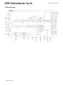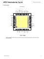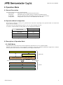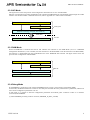
1
FEUL7105-02 ML7105 User's Manual Bluetooth Low Energy Issue Date: Nov 17, 2014 ML7105 User's Manual NOTES No copying or reproduction of this document, in part or in whole, is permitted without the consent of LAPIS Semiconductor Co., Ltd. The content specified herein is subject to change for improvement without notice. Examples of application circuits, circuit constants and any other information contained herein illustrate the standard usage and operations of the Products. The peripheral conditions must be taken into account when designing circuits for mass production. Great care was taken in ensuring the accuracy of the information specified in this document. However, should you incur any damage arising from any inaccuracy or misprint of such information, LAPIS Semiconductor shall bear no responsibility for such damage. The technical information specified herein is intended only to show the typical functions of and examples of application circuits for the Products. LAPIS Semiconductor does not grant you, explicitly or implicitly, any license to use or exercise intellectual property or other rights held by LAPIS Semiconductor and other parties. LAPIS Semiconductor shall bear no responsibility whatsoever for any dispute arising from the use of such technical information. The Products specified in this document are intended to be used with general-use electronic equipment or devices (such as audio visual equipment, office-automation equipment, communication devices, electronic appliances and amusement devices). The Products specified in this document are not designed to be radiation tolerant. While LAPIS Semiconductor always makes efforts to enhance the quality and reliability of its Products, a Product may fail or malfunction for a variety of reasons. Please be sure to implement in your equipment using the Products safety measures to guard against the possibility of physical injury, fire or any other damage caused in the event of the failure of any Product, such as derating, redundancy, fire control and fail-safe designs. LAPIS Semiconductor shall bear no responsibility whatsoever for your use of any Product outside of the prescribed scope or not in accordance with the instruction manual. The Products are not designed or manufactured to be used with any equipment, device or system which requires an extremely high level of reliability the failure or malfunction of which may result in a direct threat to human life or create a risk of human injury (such as a medical instrument, transportation equipment, aerospace machinery, nuclear-reactor controller, fuel-controller or other safety device). LAPIS Semiconductor shall bear no responsibility in any way for use of any of the Products for the above special purposes. If a Product is intended to be used for any such special purpose, please contact a ROHM sales representative before purchasing. If you intend to export or ship overseas any Product or technology specified herein that may be controlled under the Foreign Exchange and the Foreign Trade Law, you will be required to obtain a license or permit under the Law. Copyright 2013-2014 LAPIS Semiconductor Co., Ltd. 2-4-8 Shinyokohama, Kouhoku-ku, Yokohama 222-8575, Japan http://www.lapis-semi.com/en/ FEUL7105-02 i ML7105 User's Manual Preface This user's manual describes the operation and control of ML7105, a 2.4 GHz-band radio communication LSI conforming to Bluetooth® Low Energy. The following related manuals are available and should be referenced as needed: ML7105-XXX Datasheet Bluetooth Application Controller Interface (BACI) Command Manual Application Developer’s Guide for ML7105 ML7105-XXX Hardware Design Manual •Bluetooth® is a registered trademark of Bluetooth SIG, Inc. •All other company and product names are the trademarks or registered trademarks of the respective companies. FEUL7105-02 ii ML7105 User's Manual Notation Classification Notation Description z Numeric value 0xnn 0bnnnn Represents a hexadecimal number. Represents a binary number. z Address 0xnnnn_nnnn Represents a hexadecimal number.(indicates 0xnnnnnnnn) z Unit word, W byte, B Mega, M Kilo, K (uppercase) Kilo, k (lowercase) Milli, m Micro,μ Nano, n Second, s (lowercase) 1 word = 32 bits 1 byte = 8 bits 106 210=1024 103=1000 10-3 10-6 10-9 Second z Term "H" level Signal level on the high voltage side; indicates the voltage level of VIH and VOH as defined in electrical characteristics. Signal level on the low voltage side; indicates the voltage level of VIL and VOL as defined in electrical characteristics. "L" level z Register description Read/write attribute: R indicates read-enabled; W indicates write-enabled. MSB: Most significant bit in an 8-bit register (memory) LSB: Least significant bit in an 8-bit register (memory) FEUL7105-02 iii ML7105 User's Manual Table of Contents NOTES ............................................................................................................................................................................i Preface............................................................................................................................................................................ii Notation ........................................................................................................................................................................iii Table of Contents ...........................................................................................................................................................iv 1. General Description .................................................................................................................................................... 1 1.1 Features ................................................................................................................................................................ 1 1.2 Block Diagram ....................................................................................................................................................... 2 1.3 Pin Layout.............................................................................................................................................................. 3 1.4 List of Pins ............................................................................................................................................................. 4 2. Operation Mode .......................................................................................................................................................... 5 2.1 General Description............................................................................................................................................... 5 2.2 Operation Mode Configuration .............................................................................................................................. 5 2.3 Description of Operation Mode.............................................................................................................................. 5 2.3.1 BACI Mode ...................................................................................................................................................... 5 2.3.2 HCI Mode ........................................................................................................................................................ 6 2.3.3 RAM Mode ...................................................................................................................................................... 6 2.3.4 Debug Mode.................................................................................................................................................... 6 2.4 Boot Sequence ...................................................................................................................................................... 7 3. Host Interface Specifications ...................................................................................................................................... 9 3.1 General Description............................................................................................................................................... 9 3.2 Connection to Host ................................................................................................................................................ 9 3.2.1 BACI Mode ...................................................................................................................................................... 9 3.2.2 HCI Mode ...................................................................................................................................................... 12 3.2.3 RAM Mode .................................................................................................................................................... 12 3.3 SPI Interface Specifications................................................................................................................................. 12 3.4 UART Interface Specifications............................................................................................................................. 13 3.5 I2C Interface Specifications................................................................................................................................. 13 3.6 Low-power Clock ................................................................................................................................................. 13 4. BACI Interface .......................................................................................................................................................... 14 5. EEPROM Control Function....................................................................................................................................... 15 5.1 EEPROM Support ............................................................................................................................................... 15 5.1.1 User Scenarios.............................................................................................................................................. 15 5.1.1.1 EEPROM_IS_CONNECTED & EEPROM_IS_VALID .............................................................................................. 15 5.1.1.2 EEPROM_IS_NOT_CONNECTED .......................................................................................................................... 16 5.2 EEPROM Contents.............................................................................................................................................. 17 5.2.1 EEPROM Areas ............................................................................................................................................ 17 5.2.2 EEPROM Config Area................................................................................................................................... 17 5.2.3 EEPROM Configuration Parameters ............................................................................................................ 18 5.3 EEPROM Access................................................................................................................................................. 20 5.3.1 EEPROM Access and Power Supply............................................................................................................ 20 5.3.2 EEPROM Read/Write via BACI..................................................................................................................... 21 5.3.3 EEPROM Read/Write via HCI....................................................................................................................... 21 6. Power Management.................................................................................................................................................. 22 6.1 Power Mode ........................................................................................................................................................ 22 6.1.1 General Description ...................................................................................................................................... 22 6.2 Power State Transition......................................................................................................................................... 23 6.3 Wakeup Factor .................................................................................................................................................... 24 6.4 Current Profile ..................................................................................................................................................... 24 7. RF Test Mode & Direct Test Mode ............................................................................................................................ 25 7.1 Overview.............................................................................................................................................................. 25 FEUL7105-02 iv ML7105 User's Manual 7.2 Procedure Using BACI-SPI (BACI Command).................................................................................................... 25 7.3 Procedure Using HCI-UART (HCI Command & HCI Vendor Command) ........................................................... 26 8. Calibration................................................................................................................................................................. 28 8.1 Calibration Method .............................................................................................................................................. 28 8.1.1 Calibration after Hardware Reset Release ................................................................................................... 28 8.1.2 Calibration at Temperature/Voltage Change ................................................................................................. 29 8.2 Temperature Sensor ............................................................................................................................................ 31 8.3 Battery Monitor .................................................................................................................................................... 31 9. Transmit Power Control ............................................................................................................................................ 32 9.1 How to Change Default Setting of Transmit Power............................................................................................. 32 9.2 How to Dynamically Control Transmit Power ...................................................................................................... 32 10. RF Register............................................................................................................................................................. 33 10.1 General Description........................................................................................................................................... 33 10.2 RF Test Related Registers................................................................................................................................. 33 10.2.1 RF Register 0 (RF Channel) ....................................................................................................................... 33 10.2.2 RF Register 5 (Control) ...............................................................................................................................33 10.2.3 RF Register 2-31 (FUSE76)........................................................................................................................ 34 10.3 Calibration Related Registers............................................................................................................................ 35 10.3.1 RF Register 2-18(CALEN_STATE) ............................................................................................................. 35 10.3.2 RF Register 20(wrOffMode) ........................................................................................................................ 35 10.4 Temperature Sensor/Battery Monitor Related Registers................................................................................... 36 10.4.1 RF Register 7 (BlockOn2) ........................................................................................................................... 36 10.4.2 RF Register 17 (GPADC_CTRL)................................................................................................................. 36 Appendix ....................................................................................................................................................................... 37 A.1 HCI Vendor commands ....................................................................................................................................... 37 A.1.1 Write Baseband Register.............................................................................................................................. 37 A.1.2 Read Baseband Register.............................................................................................................................. 39 A.1.3 Read Radio Register .................................................................................................................................... 40 A.1.4 Write Radio Register..................................................................................................................................... 41 A.1.5 Read EEPROM Data .................................................................................................................................... 42 A.1.6 Write EEPROM Data .................................................................................................................................... 43 A.1.7 Erase EEPROM Data ................................................................................................................................... 44 A.1.8 SHUTDOWN................................................................................................................................................. 45 A.1.9 SLEEP .......................................................................................................................................................... 45 A.1.10 Read Platform Register .............................................................................................................................. 46 A.1.11 Write Platform Register ...............................................................................................................................47 A.1.12 RF Set Tx HOP ........................................................................................................................................... 48 A.1.13 Config Write Complete................................................................................................................................ 49 A.1.14 Read Config Data ....................................................................................................................................... 50 A.1.15 Write Config Data........................................................................................................................................ 51 A.1.16 Enable_I2C ................................................................................................................................................. 52 A.1.17 Get EEPROM Status .................................................................................................................................. 53 A.1.18 Config TX Power......................................................................................................................................... 54 A.1.19 Wake up...................................................................................................................................................... 55 REVISION HISTORY.................................................................................................................................................... 56 FEUL7105-02 v ML7105 User's Manual 1. General Description ML7105 is a Bluetooth® Low Energy (hereafter "LE") LSI integrating RF, Baseband, microprocessor core and each peripherals, which has Bluetooth® LE compliant 2.4 GHz-band radio communication capability. ML7105 is suitable for use with clocks, remote controllers, PC peripherals, etc. which support Bluetooth® LE. 1.1 Features • Bluetooth® SIG Core Spec v4.0 compliant • Built-in low power consumption RF block • Integrated general-purpose processor Cortex-M0, which includes an interrupt controller and Sys-Tick Timer • 64KB ROM (CODE_ROM) to store programs and 16KB RAM (DATA_RAM) to store data • 12KB RAM (CODE_RAM) to store user programs • Internal baseband controller conforming to Bluetooth® LE single mode • UART for Bluetooth® Host Controller Interface • SPI_SLAVE for Custom Host Controller Interface • EEPROM or I2C (Master & Slave) for Custom Host Controller Interface • GPIO ports (shared external pins) • System Clock Timer and External Low Power Clock Timer included • Low power consumption mode • Power supply voltage 1.6V to 3.6V • Operating temperature -20°C to 70°C • Supply current Deep sleep state 0.7µA (Typ) (Low Power Clock external input) Idle state 3.0mA (Typ) At transmission 9mA (Typ) At reception 9mA (Typ) • Package 32-pin WQFN (P-WQFN32-0505-0.50-A63) Lead-Free package conforming to RoHS FEUL7105-02 1 ML7105 User's Manual 1.2 Block Diagram FEUL7105-02 2 ML7105 User's Manual 1.3 Pin Layout I2C_SCL VDDIO UART_RXD UART_TXD SPICLK SPIXCS SPIDOUT SPIDIN 32-pin WQFN 24 23 22 21 20 19 18 17 I2C_SDA 25 16 VDDCORE GPIO0 26 15 EFUSE GPIO1 27 14 XON GPIO2 28 13 XOP GNDPKG RESETB 31 10 LPCLKBUS A0 32 9 1 2 3 4 5 6 7 8 REGOUT LPCLKIN PLLLPF 11 VDDVCO 30 SWTX TMODE SWRX REGC SWOUT 12 VDDRF 29 A1 GPIO3 VDDBAT TOP VIEW NOTICE:"GNDPKG" shown in the center of the chip is located at the back surface of the chip (name: Package GND). FEUL7105-02 3 ML7105 User's Manual 1.4 List of Pins Pin Number Symbol I/O ANA/DIG IO TYPE 1 A1 IN ANA DIRIO 2 VDDRF --- PWR VCC 3 SWOUT INOUT ANA DIRIO_RF RF signal RX/TX inout 4 SWRX INOUT ANA DIRIO_RF RX SW control signal 5 SWTX INOUT ANA DIRIO_RF TX SW control signal 6 VDDVCO --- PWR VCC 7 PLLLPF OUT ANA DIRIO PLL Loop Filter 8 REGOUT OUT ANA DIRIO Regulator output 9 VDDBAT --- PWR VCC 10 LPCLKBUS INOUT ANA DIRIO Low-power clock output 11 LPCLKIN INOUT ANA DIRIO Low-power clock input 12 REGC OUT ANA DIRIO Decoupling capacitor pin for internal regulator 13 XOP INOUT ANA DIRIO Positive input/output for Xtal oscillator block 14 XON INOUT ANA DIRIO Negative input/output for Xtal oscillator block 15 EFUSE --- DIG DIRIO Power supply for E-Fuse (Normal: GND) 16 VDDCORE --- PWR VCC 17 SPIDIN IN DIG 18 SPIDOUT INOUT DIG 19 SPIXCS IN DIG CMOS, IN SPI Slave Chip Select 20 SPICLK IN DIG CMOS, IN SPI Slave Clock 21 UART_TXD OUT DIG CMOS, OUT UART TXD output 22 UART_RXD IN DIG CMOS, IN UART RXD input 23 VDDIO --- PWR 24 I2C_SCL INOUT DIG 25 I2C_SDA INOUT DIG INOUT DIG INOUT DIG INOUT DIG INOUT DIG IN DIG CMOS, IN TESTMODE input CMOS, IN Reset input 26 27 28 29 GPIO0 /RF_ACTIVE GPIO1 /WAKEUP GPIO2 /IRQ GPIO3 /PS_CONTROL Description General-purpose analog input Power supply for RF block (1.2 V) Power supply for RF-VCO (1.2V) Power supply from Battery (= VDDIO) Power supply for digital core (1.2V) CMOS, IN SPI Slave Data input CMOS, BiDIR VCC CMOS, BiDIR CMOS, BiDIR CMOS, BiDIR CMOS, BiDIR CMOS, BiDIR CMOS, BiDIR SPI Slave Data output Power supply for digital IO I2C_SCL I2C_SDA GPIO input-output/RF_ACTIVE GPIO input-output/WAKEUP GPIO input-output/IRQ GPIO input-output/external switch control signal 30 TMODE 31 RESETB IN DIG 32 A0 IN ANA DIRIO General-purpose analog input G GNDPKG --- GND GND Package GND For details of each pin, refer to ML7105-XXX Datasheet. FEUL7105-02 4 ML7105 User's Manual 2. Operation Mode 2.1 General Description ML7105 has the following four operation modes. BACI Mode: Application mode using the SPI-SLAVE interface HCI Mode: HCI Mode using the UART interface (compliant with Bluetooth LE) RAM Mode: Function extension mode downloading a user program to internal memory Debug Mode: Debug Mode to have access to I2C-EEPROM write and read 2.2 Operation Mode Configuration When starting of ML7105, set the pin as specified in the table below, depending on the operation mode. "X" means that any pin state is acceptable. The mode cannot be changed during operation. Use reset when changing the mode. To switch to the RAM Mode or Debug Mode, use the configuration parameters. Pin setting value Operation Mode UART_RXD BACI Mode Low HCI Mode High RAM Mode X Debug Mode X * 1 When using the LSI in HCI Mode, fix the WAKEUP pin to LOW. 2.3 Description of Operation Mode 2.3.1 BACI Mode The figure below shows the protocol stack configuration when ML7105 is set to the BACI Mode. ML7105 can transmit/receive various messages (commands, events, data) defined by Bluetooth Application Controller Interface (BACI) described later to/from HOST-CPU through the SPI interface. Application Profile (VSP, HRP, etc) HOST_CPU Bluetooth Application Controller Interface (BACI) Host SPI (BACI) Bluetooth Application Controller Interface (BACI) Controller Bluetooth Low Energy Host (GAP, GATT, SMP, etc) ML7105 Bluetooth Low Energy Controller (LL, etc) FEUL7105-02 5 ML7105 User's Manual 2.3.2 HCI Mode The figure below shows the protocol stack configuration when ML7105 is set to the HCI Mode. ML7105 can transmit/receive HCI commands/events compliant with Bluetooth LE to/from HOST-CPU through the UART interface. For the HCI Vendor commands of this LSI, refer to Appendix A.1 "HCI Vendor commands". Application Profile (VSP, HRP, etc) HOST_CPU Bluetooth Low Energy Host (GAP, GATT, SMP, etc) UART (HCI) Bluetooth Low Energy Controller (LL, etc) ML7105 2.3.3 RAM Mode When an EEPROM is connected and the bit that indicates the transition to the RAM Mode (see 5.2.3 "EEPROM Configuration Parameters") is set to Enable, the state transitions to the RAM Mode. After the transition to the RAM Mode, the firmware is downloaded from the CODE-RAM area of the EEPROM and executed. The figure below shows the protocol stack configuration of RAM Mode. Application Profile (VSP, HRP, etc) ML7105 Bluetooth Low Energy Host (GAP, GATT, SMP, etc) Bluetooth Low Energy Controller (LL, etc) 2.3.4 Debug Mode If no EEPROM is connected or if the content of EEPROM is not correct(*), the LSI starts in the Debug Mode. In this mode, the Bluetooth functions cannot be used. Only the minimum necessary initialization is performed, and the LSI waits for the configuration parameters to be set. In this mode, it is possible to load the configuration parameters from HOST_CPU via BACI or HCI or to initialize (write/read) the EEPROM. (*) When EEPROM_VALID_CODE is not 0x5A (EEPROM_IS_NOT_VALID) FEUL7105-02 6 ML7105 User's Manual 2.4 Boot Sequence The ML7105 boot sequence is shown below. Start (Power On & Hardware Reset) Reset Handler Wakeup or Config is Valid Retention Status Register ? Not Wakeup or Config is Ivalid Check external pins by GPIO “EEPROM_IS_CONNECTED” Yes Load Config from EEPROM I2C_SDA == High ? No “EEPROM_IS_NOT_CONNECTED” Is Config Valid? No (== 0x5A) “EEPROM_IS_NOT_VALID” Yes “EEPROM_IS_VALID” Check external pins by GPIO UART_RX == High ? No No SPI_SLAVE (BACI) Initialization for Loading I/F Yes Check external pins by GPIO is not required UART0 (HCI) Initialization for Loading I/F Load Config Parameters (Debug Mode) FEUL7105-02 7 ML7105 User's Manual Check Parameter Value RAM Mode ROM or RAM Mode ? ROM Mode Check external pins by GPIO Yes UART_RX == High? No Go to GATT & GAP I/F (SPI_SLAVE) for Application and TEST (BACI Mode) Go to HCI I/F (UART0) for Application and TEST (HCI Mode) Go to User Application (RAM Mode) Disable Pull-Down of UART_RXD pin Download User Application to CODE_RAM Restore Remap Normal Operation Call Reset Handler No Can Shutdown? Yes No Wakeup Pin == High ? Yes Store & Retention Status = Wakeup FEUL7105-02 8 ML7105 User's Manual 3. Host Interface Specifications 3.1 General Description ML7105 has the following two types of host interfaces. «SPI interface – BACI Mode» An interface to use the SPI-SLAVE of ML7105. By controlling this interface, the host system can exchange commands and events through the SPI. «UART interface – HCI Mode » An interface to use the UART of ML7105. By controlling this interface, the host system can exchange commands and events through the UART. 3.2 Connection to Host 3.2.1 BACI Mode The connection to the host consists of the SPI_SLAVE interface and three GPIOs. The example below shows the configuration when connecting to the host using the SPI_SLAVE. GPIO (Input) (Input) RF_ACTIVE GPIO WAKEUP (Output) (Output) GPIO (Input) HOST_CPU (Application Processor) U8 SCK GPIO0 / RF_ACTIVE GPIO1 / WAKEUP (Input) IRQ GPIO2 / IRQ (Output) SPICLK (Output) (Input) SOUT SPIDIN (Output) (Input) SIN SPIDOUT (Input) (Output) GPIO SPIXCS (Output) ML7105 (Bluetooth LE LSI) (Input) The three GPIOs serve the following functions: RF_ACTIVE: Indicates that Bluetooth communication is being made (large current consumption). At return to the IDLE state from the power-down or Deep Sleep state, rush current occurs. At return from Deep Sleep by the internal timer, this pin notifies the rush current. At power-on or at return from Deep Sleep by the WAKEUP pin, this pin does not notify the rush current. After power-on, if an EEPROM is connected, the AUTO calibration is executed. During the execution, RF_ACTIVE turns to High. On the other hand, if no EEPROM is connected, the AUTO calibration is not executed. Therefore RF_ACTIVE does not turn to High. WAKEUP: This signal indicates the REQUEST or the READY state from the host to ML7105. When starting the SPI communication (REQUEST), control this pin as Low. IRQ: FEUL7105-02 This signal indicates the REQUEST or READY state from ML7105 to the host. When ML7105 transitions to the READY state for the REQUEST from the host, ML7105 toggles this pin to Low. The REQUEST from ML7105 is also notified by toggling this pin to Low. 9 ML7105 User's Manual Each pin behaves as follows: The normal state of the RF_ACTIVE pin is Low. The normal states of the WAKEUP, IRQ, and SPIXCS pins are High. The SPI communication is performed in the following sequence: - Communication request from HOST 1. HOST toggles the WAKEUP pin to Low. 2. When ML7105 detects WAKEUP and goes to the READY state, ML7105 toggles the IRQ pin to Low. 3. HOST starts the SPI communication. During the communication, HOST toggles the SPIXCS pin to Low. 4. When the SPI communication is completed, HOST toggles the WAKEUP pin to High. 5. When ML7105 detects that the WAKEUP pin turns to High, ML7105 toggles the IRQ pin to High. [Note] When transmitting dummy data other than BACI packet from HOST, be sure to transmit 0xFF. Please add 0xFF at the end of BACI packet from HOST. - Communication request from ML7105 (when transmitting one BACI packet ) 1. ML7105 toggles the IRQ pin to Low. 2. When HOST detects IRQ and goes to the READY state, HOST toggles the WAKEUP pin to Low. 3. HOST starts the SPI communication. During the communication, HOST toggles the SPIXCS pin to Low. ML7105 outputs the dummy data (0xFF) and then starts the transmission of the BACI packet. 4. ML7105 starts transmitting the BACI packet. 5. When HOST completes receiving the BACI packet, HOST must toggle the WAKEUP pin to High. 6. When ML7105 detects that the WAKEUP pin turns to High, ML7105 toggles the IRQ pin to High. - Timing control when a communication request from HOST is made After toggling the IRQ signal to High, ML7105 transitions to the Deep Sleep mode if no communication request from HOST is made for a specified period (about 1 ms). During this transition to the Deep Sleep mode, no communication request from HOST is accepted. Therefore, insert a WAIT of 3 ms or more after toggling the WAKEUP signal to High before toggling it to Low, so that a communication request from HOST can be accepted. If there is no IRQ signal response to the communication request from HOST, perform the retry process (toggle the WAKEUP signal back to High and then toggle it to Low again). FEUL7105-02 10 ML7105 User's Manual - Communication request from ML7105 (when transmitting two BACI packets continuously) 1. ML7105 toggles the IRQ pin to Low. 2. When HOST detects IRQ and goes to the READY state, HOST toggles the WAKEUP pin to Low. 3. HOST starts the SPI communication. During the communication, HOST toggles the SPIXCS pin to Low. ML7105 outputs the dummy data (0xFF) and then starts the transmission of the BACI packet. 4. When HOST completes receiving the BACI packet, HOST must toggle the WAKEUP pin to High. 5. If there are more BACI packets to be transmitted continuously, ML7105 keeps IRQ in the Low state. 6. When HOST detects that IRQ is in the Low state, HOST must toggle the WAKEUP pin to Low. 7. HOST starts the SPI communication. During the communication, HOST toggles the SPIXCS pin to Low. ML7105 outputs the dummy data (0xFF) and then starts the transmission of the second BACI packet. 8. When HOST completes receiving the BACI packet, HOST must toggle the WAKEUP pin to High. 9. When ML7105 detects that the WAKEUP pin turns to High, ML7105 toggles the IRQ pin to High. The RF_ACTIVE pin behaves as follows: FEUL7105-02 11 ML7105 User's Manual The RF_ACTIVE pin outputs High during the period of RF communication or calibration where an increased current is required. The RF_ACTIVE pin outputs High also at return from Deep Sleep by the internal timer, since the current increases due to the rush current. The RF_ACTIVE pin outputs High during the T_rf_act period before the current increases. The value of T_rf_act varies depending on the cause to be notified. When RF_ACTIVE notifies the current increase due to RF communication, T_rf_act is 625 µsec * 2 = about 1.2 msec or 625 µsec *3 = about 1.8 msec. On the other hand, T_rf_act is about 1 msec at return from Deep Sleep. The RF_ACTIVE pin is toggled to Low when the RF communication is completed or at transition to Deep Sleep. While the RF communication continues, the RF_ACTIVE pin always outputs High. At a return from power-down or at a return to IDLE from Deep Sleep by the WAKEUP pin, the current increases due to the rush current just like the case at the return from Deep Sleep by the internal timer. However, the RF_ACTIVE pin does not output High in this case. 3.2.2 HCI Mode The connection to the host consists of the UART interface. The example below shows the configuration when connecting to the host using the UART. When using the ML7105 in HCI Mode, fix the WAKEUP pin to Low. 3.2.3 RAM Mode In the RAM Mode, the connection to the host is not necessary. 3.3 SPI Interface Specifications Table 1 shows the specifications of the SPI interface used in the BACI Mode. Table 1 SPI Interface Specifications Parameter Bit rate SPI mode Data size Chip select FEUL7105-02 Specification Typ. 32.768KHz Max. 1.625MHz MSB First, Positive Edge 8 bits Low Active 12 ML7105 User's Manual 3.4 UART Interface Specifications Table 2 shows the specifications of the UART interface used in the HCI Mode. Table 2 UART Interface Specifications Parameter Specification Baud rate 57600bps Data size 8 bits Parity bit No parity Stop bit 1 stop bit Flow control No 3.5 I2C Interface Specifications Table 3 shows the specifications of the I2C interface for connecting an EEPROM. Table 3 I2C Interface Specifications Parameter Specification Master/Slave Master Data rate 220kHz Address bit 7 bit Data bit 8 bit Protocol None 3.6 Low-power Clock The Low-power clock (LPCLK) is used in the operation at low power consumption. Normally, always supply a 3.3 V clock (32.768 KHz) to the LPCLKIN pin. Table 4 shows the relationship between the operation mode and the necessity of LPCLK supply. Table 4 Necessity of LPCLK Supply for Each Operation Mode Operation mode BACI Mode HCI Mode FEUL7105-02 Necessity of LPCLK supply LPCLK always must be supplied. LPCLK does not need to be supplied. 13 ML7105 User's Manual 4. BACI Interface In the BACI Mode using the SPI interface, various messages (commands, events, and data) are exchanged through the BACI interface. * For details of the BACI interface, refer to the document "Bluetooth Application Controller Interface(BACI) Command Manual". FEUL7105-02 14 ML7105 User's Manual 5. EEPROM Control Function 5.1 EEPROM Support At the time of starting, ML7105 detects the existence of EEPROM device connected to the I2C interface. If an EEPROM device is connected, ML7105 further reads EEPROM_VALID_CODE written to the EEPROM device and detects whether or not to use the EEPROM as the storage memory of Configuration parameters. I2C_SDA Pin Low (EEPROM_IS _NOT_CONNECTED) High (EEPROM_IS _CONNECTED) High (EEPROM_IS _CONNECTED) EEPROM_VALID_CODE Location of Configuration Parameters None HOST_CPU (ML7105 receive them via SPI) 0x5A (EEPROM_IS_VALID) EEPROM (ML7105 get them via I2C) 0xXX (EEPROM_IS_NOT_VALID) HOST_CPU (ML7105 receive them via SPI) EEPROM_VALID_CODE is stored at address 0x04 in the EEPROM. 5.1.1 User Scenarios 5.1.1.1 EEPROM_IS_CONNECTED & EEPROM_IS_VALID If an EEPROM is used, ML7105 operates in the following configuration: HOST_CPU BACI ML7105 I2C EEPROM Parameters (1) When the Configuration parameters have been written Step 1. Power ON, Hardware Reset. Step 2. ML7105 detects “EEPROM_IS_CONNECTED”. Step 3. ML7105 configures the I2C interface. Step 4. ML7105 reads 1 byte for EEPROM_VALID_CODE from EEPROM. Step 5. ML7105 detects “EEPROM_IS_CONNECTED & EEPROM_IS_VALID”. Step 6. ML7105 configures the BACI interface. Step 7. ML7105 reads Configuration parameters from EEPROM. Step 8. ML7105 initializes by Configuration Parameters. Step 9. ML7105 sends “Start Up” (*State 0x80) event message to HOST_CPU via BACI. *State 0x80 indicates that Normal startup. Step 10. ML7105 waits BACI Command. (2) When the Configuration parameters have not been written Step 1. Power ON, Hardware Reset. Step 2. ML7105 detects “EEPROM_IS_CONNECTED”. Step 3. ML7105 configures the I2C interface. Step 4. ML7105 reads 1 byte for EEPROM_VALID_CODE from EEPROM. Step 5. ML7105 detects “EEPROM_IS_CONNECTED & EEPROM_IS_NOT_VALID”. Step 6. ML7105 configures the BACI interface. Step 7. ML7105 sends “Start Up” (*State 0x82) event message to HOST_CPU via BACI. *State 0x82 indicates that EEPROM is connected and the request for Get Configuration parameters. Step 8. HOST-CPU sends “Enable_I2C” (Parameter = 0x01) Command. Step 9. HOST-CPU sends “Write EEPROM” Command to write the CONFIG parameters to EEPROM. This command will be repeated to write all the Configuration parameters (128Byte). Step 10. Hardware Reset. For the subsequent steps, refer to the steps described above in "(1) When the Configuration parameters have been written". FEUL7105-02 15 ML7105 User's Manual 5.1.1.2 EEPROM_IS_NOT_CONNECTED If an EEPROM is not used, ML7105 operates in the following configuration: HOST_CPU BACI ML7105 Parameters Step 1. Step 2. Step 3. Step 4. Step 5. Step 6. Step 7. Step 8. FEUL7105-02 Power ON, Hardware Reset. ML7105 detects “EEPROM_IS_NOT_CONNECTED”. ML7105 configures the BACI interface. ML7105 sends “Start Up” (*State 0x81) event message to HOST_CPU via BACI. *State 0x81 indicates that EEPROM is not connected and request for Get Configuration parameters. ML7105 waits BACI command for Write_Config from HOST_CPU. ML7105 finish the receiving the Configuration Parameters from HOST_CPU. After finish sending the Configuration parameters, HOST_CPU sends WRITE_CONFIG_COMPLETE BACI command. ML7105 modifies RETENTION_RAM status with valid configuration. ML7105 initializes by Configuration Parameters. ML7105 sends “Start Up” (*State 0x80) event message to HOST_CPU via BACI. *State 0x80 indicates that Normal startup. ML7105 waits BACI Command. 16 ML7105 User's Manual 5.2 EEPROM Contents 5.2.1 EEPROM Areas The data storage areas of EEPROM vary depending on EEPROM_VALID_CODE and RAM_Mode. The basic configuration of EEPROM is described below. Address 0x00 Configuration Area Address 0x80 Application Area Address 0x800 The setting parameters of Baseband and RF are stored in the Configuration Area. The Application Area is the area that HOST_CPU can use arbitrarily. CODE_RAM Area The program code of RAM_Mode is stored in the CODE_RAM Area. The storage area for each combination of EEPROM_VALID_CODE and RAM_Mode flag is described below. EEPROM_VALID_CODE (#1) RAM_Mode flag (#2) EEPROM Contents ML7105 uses the addresses 0x00 to 0x7E of EEPROM as Configuration Area. Disable HOST_CPU can use the addresses after 0x80 of EEPROM as Application Area. ML7105 uses the addresses 0x00 to 0x7E of EEPROM as Configuration Area and uses the addresses after 0x800 of EEPROM as CODE_RAM Area. 0x5A Enable HOST_CPU can use the addresses 0x80 to 0x7FF of (EEPROM_IS_VALID) EEPROM and the areas other than the CODE_RAM Area as Application Area. The state where writing Configuration parameters to the 0xXX --EEPROM is not completed. (EEPROM_IS_NOT_VALID) (#1) EEPROM_VALID_CODE is stored at the address 0x04 of EEPROM. (#2) RAM_Mode flag is stored at the address 0x38 of EEPROM. 0x5A (EEPROM_IS_VALID) The maximum EEPROM address space that ML7105 can access is 64 KB (address 0xFFFF). 5.2.2 EEPROM Config Area The Configuration Area stored in the EEPROM consists of a header and parameters. The basic configuration of Configuration Area is described below. Address 0x00 7C 00 00 00 5A 50 1B 00 6A 00 .. .. .. Configuration header (4Byte) Configuration parameters (124Byte) Configuration header indicates the size of Configuration parameters. In normal cases, it is 0x7C (124). The Configuration parameters consists the setting parameters of Baseband and RF. FEUL7105-02 17 ML7105 User's Manual 5.2.3 EEPROM Configuration Parameters The default Configuration parameters are described below. (1) When EEPROM is used Follow the procedure described in "5.1.1.1 EEPROM_IS_CONNECTED & EEPROM_IS_VALID" to set the following Configuration parameters to the Configuration Area of EEPROM. - Default Configuration Parameters for ML7105-XXX (Ver4.02) [When EEPROM is used] 00 01 02 03 04 05 06 07 08 09 0A 0B 0C 0D 0E 0F EEPROM Address -------------------------------------------------------------------------: 7c 00 00 00 5a 50 1b 00 79 01 00 00 20 aa e2 10 0x10 : 3a e0 18 e0 00 00 ff 00 04 be 1e 90 40 06 01 50 EEPROM Address 0x20 EEPROM Address 0x30 EEPROM Address 0x40 EEPROM Address 0x50 EEPROM Address 0x60 EEPROM Address 0x70 EEPROM Address 0x00 : : : : : : 0a d1 05 74 30 00 03 d2 71 84 00 00 18 d3 05 34 30 04 00 d3 71 34 00 00 be d2 fc 0a 30 ff 81 d1 2f 0a 00 ff 00 14 00 0a 30 ff 08 01 30 0a 00 ff d1 17 05 73 30 ff d2 40 71 27 00 ff d3 0c 05 73 30 ff d3 ff 71 27 00 ff d2 fc 0c 73 00 ff d1 2f b0 27 fa 00 3e 00 39 73 f4 ff 02 30 00 27 ee 00 (2) When EEPROM is not used Follow the procedure described in "5.1.1.2 EEPROM_IS_NOT_CONNECTED" to set the following Configuration parameters to the Configuration Area within ML7105. - Default Configuration Parameters for ML7105-XXX (Ver4.02) [When EEPROM is not used] 00 01 02 03 04 05 06 07 08 09 0A 0B 0C 0D 0E 0F -------------------------------------------------------------------------Configuration Address 0x00 : 5a 50 1b 00 79 01 00 00 20 aa e2 10 3a e0 18 e0 Configuration Address 0x10 : 00 00 ff 00 04 Address 0x20 : be 81 00 08 d1 Address 0x30 : d2 d1 14 01 17 Address 0x40 : fc 2f 00 30 05 be d2 Configuration 40 Configuration 71 Configuration Address 0x50 : 0a 0a 0a 0a 73 27 Configuration Address 0x60 : 30 00 30 00 30 00 Configuration Address 0x70 : ff ff ff ff ff ff Configuration FEUL7105-02 1e d3 0c 05 73 30 ff 90 d3 ff 71 27 00 ff 40 d2 fc 0c 73 00 ff 06 d1 2f b0 27 fa 00 01 3e 00 39 73 f4 ff 50 02 30 00 27 ee 00 0a d1 05 74 30 00 03 d2 71 84 00 00 18 d3 05 34 30 04 00 d3 71 34 00 00 18 ML7105 User's Manual The following are parameters you can change arbitrarily. EEPROM Address [Hex] Configuration Address [Hex] Default Value [Hex] Variable Name Note 0x04 0x01 0x5A eeprom_valid_code 0x08 0x09 0x0A 0x04 0x05 0x06 0x6A 0x00 0x00 compid adv_ch_tx_power_gain 0x0B 0x07 0x00 conn_ch_tx_power_gain 0x1C 0x1D 0x18 0x19 0x40 0x06 max_effective_ci 0x20 0x1C 0x0A wakeup_config [7:5] : 0x0 [4:2] : RF_ACTIVE_period [1:0] : 0x2 Select the transmitter power setting of the Advertising channel. 0x00: 0 dBm 0x01:-6 dBm 0x02:-12 dBm 0x03:-18 dBm Select the transmitter power setting of the Connection channel. 0x00: 0 dBm 0x01:-6 dBm 0x02:-12 dBm 0x03:-18 dBm When Slave Latency is set, the Connection interval is limited to the maximum of 2 seconds (0x0640). [Note] Changing the setting of this parameter is prohibited. RF_ACTIVE_period: Set the timing when the GPIO0/RF_ACTIVE pin is toggled to High. N = 1..5: 625µsec * n, Default = 2 0x28 | 0x2D 0x24 | 0x29 public_addr Set the Bluetooth Public Address. 0x30 | 0x35 0x2C | 0x31 satic_addr Set the Static Random Address. 0x38 0x34 0xD0 0xD1 0xD2 0xD2 0xD1 0xD0 0xD1 0xD2 0xD3 0xD3 0xD2 0xD1 0x17 general_flags_8bit [7] : 0x0 [6] : 0x0 [5] : RAM_Mode [4] : 0x1 [3] : BACI over UART [2] : 0x1 [1:0] : Enable DSM 0x4E 0x4A 0x39 - RAM_Mode: 0x0: Disabled 0x1: Enabled. - BACI over UART: Function for test. Set this bit to 0x0 for normal use. - Enable DSM: 0x0, 0x1: Reserved 0x2: DSM for RAM Mode 0x3: DSM for BACI/HCI Mode [Note] Set this bit to 0x2 in the RAM Mode, or 0x3 in the other modes. - Sleep clock accuracy : Set the Sleep Clock Accuracy based on the accuracy of the Lowpower clock which is supplied to ML7105. FEUL7105-02 general_variable [7:4] : 0x03 [3] : 0x1 [2:0] : Sleep Above-mentioned EEPROM_VALID_CODE. Normally, do not change the value 0x5A. Company ID(0x0179) clock 19 ML7105 User's Manual EEPROM Address [Hex] Configuration Address [Hex] Default Value [Hex] Variable Name accuracy Note 0x0: LPCLK≤500ppm 0x1: LPCLK≤250ppm---Default 0x2: LPCLK≤150ppm 0x3: LPCLK≤100ppm 0x4: LPCLK≤75ppm 0x5: LPCLK≤50ppm 0x6: LPCLK≤30ppm 0x7: LPCLK≤20ppm 5.3 EEPROM Access 5.3.1 EEPROM Access and Power Supply The ML7105 start sequence and the power supply procedure (to turn off the power of EEPROM) are described below. Step 1. Supply power to ML7105 and the EEPROM When the ML7105 reset is released, ML7105 performs Read Access to the EEPROM device. When starting the power supply to ML7105, always start the power supply to the EEPROM device. Step 2. ML7105 completes the access to the EEPROM When ML7105 completes the access to the EEPROM and the initialization of it, a Start Up Event message is output to HOST_CPU, if BACI is used. Step 3. HOST_CPU issues an Enable_I2C command (Parameter = 0x00) to disable the I2C interface When the I2C interface is disabled, ML7105 drives the I2C_SCL and I2C_SDA pins to Low. Step 4. Turn off the power supply of the EEPROM device. Step 5. After this, follow the steps described in "5.3.2 EEPROM Read/Write via BACI" or "5.3.3 EEPROM Read/Write via HCI" to access to the EEPROM and supply the power to it. ML7105 does not access to the EEPROM automatically except the time of starting mentioned above. After the starting time, ML7105 accesses to the EEPROM only when it is directed to do so by any BACI or HCI Vendor command. FEUL7105-02 20 ML7105 User's Manual 5.3.2 EEPROM Read/Write via BACI The procedure for the Read/Write access to the EEPROM data using the BACI commands is described below. (It is assumed that the power of the EEPROM device is turned off during the period when no access to the EEPROM is made.) Step 1. Supply the power to the EEPROM device Step 2. Use the Enable_I2C command (Parameter = 0x01) to enable the I2C interface Step 3. Use the GET_EEPROM_Status command to check the EEPROM status 0x0 (EEPROM_ENABLED_VALID) is returned. This command is not always required to be issued. Step 4. Execute Read EEPROM or Write EEPROM These commands can be executed repeatedly. Step 5. Use an Enable_I2C command (Parameter = 0x00) to disable the I2C interface Step 6. Turn off the power supply of the EEPROM device 5.3.3 EEPROM Read/Write via HCI The procedure for the Read/Write access to the EEPROM data using the HCI Vendor commands is described below. (It is assumed that the power of the EEPROM device is turned off during the period when no access to the EEPROM is made.) Step 1. Supply the power to the EEPROM device Step 2. Use the HCI_VENDOR_ENABLE_I2C command (Parameter = 0x01) to enable the I2C interface Step 3. Use the HCI_VENDOR_GET_EEPROM_STATUS command to check the EEPROM status 0x0 (EEPROM_ENABLED_VALID) is returned. This command is not always required to be issued. Step 4. Execute HCI_VENDOR_EEPROM_READ or HCI_VENDOR_EEPROM_WRITE These commands can be executed repeatedly. Step 5. Use the HCI_VENDOR_ENABLE_I2C command (Parameter = 0x00) to disable the I2C interface Step 6. Turn off the power supply of the EEPROM device FEUL7105-02 21 ML7105 User's Manual 6. Power Management 6.1 Power Mode 6.1.1 General Description ML7105 has the following operation modes. [Active mode] The Active Mode is a mode used during a period of connection with radio communication (during transmission and reception). [Idle mode] ML7105 transits to this mode after a short communication interval which is equal to or less than 15msec. [Deep sleep mode] ML7105 transits to the Deep Sleep mode after a long communication interval or when no access is made by HOST for a certain time in a non-communication period. The RF oscillation is stopped and the communication interval is counted by the Low-power clock from an external pin. [Application Sleep] During the Application Sleep mode, the RF oscillation is stopped and ML7105 is in wait state while operating on the Low-power clock from an external pin. When HOST_CPU issues the Sleep command, ML7105 goes to this state and waits until the Wakeup by HOST_CPU. FEUL7105-02 22 ML7105 User's Manual 6.2 Power State Transition The power mode state transition diagram of ML7105 is shown in Figure 1. Figure 1 Power state transition and operating mode [Power On] When the power supply starts, assert the hardware reset for a certain period. When the hardware reset is released, ML7105 transits to the Boot State. [Boot State] When the hardware reset is released, the boot is started. The boot program initializes the peripherals and loads the parameters. [Connection State] ML7105 operates in the Active mode during the period of radio communication connection or during the application processing period. [Short Interval or Application Processing State] ML7105 operates in the Idle mode during a short time period (≦15msec) of waiting for radio communication or during the simple application processing period. [Long Interval State] ML7105 transits to the Deep Sleep mode during a long time period of waiting for radio communication or when no access is made by HOST for a certain time in a non-communication period. ML7105 operates only with the 32.768 KHz Low Power Clock from an external pin in Deep Sleep mode. (Note) In this state, the communication interval is counted by the internal timer, enabling ML7105 to return from the Deep Sleep mode temporarily at the timer expiration (at about 40-second interval). When you want to keep the Deep Sleep state, make a transition to the Sleep State. FEUL7105-02 23 ML7105 User's Manual [Sleep State] During the Sleep State, the 26 MHz clock of RF is stopped, and ML7105 waits for Wakeup while operating on the Low Power Clock (Typ. 32.768 KHz) from an external pin. When HOST_CPU issues the Sleep command, ML7105 goes to this state and waits until the Wakeup by HOST_CPU. (Note) In the HCI Mode, the transition to the Long Interval State or Sleep State is not performed. 6.3 Wakeup Factor The return from the Deep Sleep mode or the Application Sleep mode is performed by Wakeup Factor. After the detection of the Wakeup Factor of the Low state of the GPIO1/WAKEUP pin, RF starts a 26 MHz oscillation. 6.4 Current Profile The following shows the state transition of operation current starting from the activation from the Deep Sleep mode, through the completion of transmission/reception, and then returning to the Deep Sleep Mode, using the case of BACI Mode as an example. Current Irash Itx, Irx Iifs Iboot Irfinit Iidle Istby Idsm Time Tdsm Trash Txo-idle Tboot Status Trfinit Tinit Trx Tifs Definition Tdsm Deep sleep period depend on connection interval Trash Spike from voltage regulator wake-up Txo_idle Start up time for Xtal oscillator block for systems clock 26MHz Tboot System is in booting operation Trfinit Initialize RF register Tinit Pre-processing after deep sleep mode Trx Packet reception Tifs Time between RX to TX operation Ttx Packet transmission Tdwn Post processing before moving to deep sleep operation FEUL7105-02 Ttx Tdwn 24 ML7105 User's Manual 7. RF Test Mode & Direct Test Mode 7.1 Overview ML7105 transits to the RF Test Mode by execution of the BACI-SPI or HCI-UART command. The RF Test Mode is assumed to be used for the following tests: 1. RF Test conforming to Bluetooth (Direct Test Mode) 2. Technical conformance test in Japan 7.2 Procedure Using BACI-SPI (BACI Command) The pin handling to use BACI-SPI to make a transition to RF Test Mode is described in Table 5. Table 5 Pin Condition of RF Test Mode via BACI-SPI Pin Name LPCLKIN SPIDIN SPIDOUT SPIXCS SPICLK UART_TXD UART_RXD I2C_SCL I2C_SDA GPIO0 GPIO1 GPIO2 Condition/Configuration Note Required (32.768KHz Clock Input) Required (Connected to HOST_CPU) Required (Connected to HOST_CPU) Required (Connected to HOST_CPU) Required (Connected to HOST_CPU) Not required (Open) Required (Open or Low Input) Depend on EEPROM connection Depend on EEPROM connection Active (RF_ACTIVE Output) Required (WAKEUP Input) Required (IRQ Output) The control procedure of the RF Test using BACI-SPI is as follows: Step 1. Set ML7105 to BACI Mode and supply the power. Step 2. Release the ML7105 reset. Step 3. When ML7105 completes the initialization, ML7105 outputs a Start Up Event message to HOST_CPU. Step 4. HOST_CPU issues the Test command (Parameter = 0x01:Test Mode Enabled) to ML7105. Step 5. HOST_CPU issues the DTM command to ML7105 and starts the Direct Test Mode. Step 6. HOST_CPU issues the Test command (Parameter = 0x00:Test Mode Disabled) to ML7105, and completes the RF Test. FEUL7105-02 25 ML7105 User's Manual The control procedure of the technical conformance test using BACI-SPI is as follows: Step 1. Set ML7105 to BACI Mode and supply the power. Step 2. Release the ML7105 reset. Step 3. When ML7105 completes the initialization, ML7105 outputs a Start Up Event message to HOST_CPU. [Transmission test, Single channel] Step 4-1. HOST_CPU issues the Test command (Parameter = 0x01:Test Mode Enabled) to ML7105. Step 4-2. HOST_CPU issues the DTM command to ML7105 and starts the Direct Test Mode (TX). ML7105 repeats transmissions at a single channel. [Transmission test, All channel search] Step 4-1. HOST_CPU issues the Test command (Parameter = 0x01:Test Mode Enabled) to ML7105. Step 4-2. HOST_CPU issues the RF Set Tx Hop command (Parameter = 0x01: Enable Hop for all channels) to ML7105. Step 4-3. HOST_CPU issues the DTM command to ML7105 and starts the Direct Test Mode (TX). ML7105 repeats transmissions for all channels incrementing the channel. [Continuous transmission test] Step 4-0. HOST_CPU issues the RF Set Tx HOP command (Hop=0x00) to ML7105. Step 4-1. HOST_CPU issues the Read RF Reg command to read RF Register 2-31 (Address: 0x3F). The value of D[15:8] in this read data is the setting value for D[15:8] of RF Register 0 (Address 0x00) described in the next section. In this example, the case where the read result is 0x00 0x00 0x30 0x** is used. Step 4-2. HOST_CPU issues the Write RF Reg command to set the following to the RF register. RF Register0 (Address : 0x00) : Write_Data 0x3005 RF Register5 (Address : 0x05) : Write_Data 0x2712 Step 4-3. ML7105 goes to the continuous transmission state. Step 4-4. At completion, HOST_CPU issues the Write RF Reg command to set the following to the RF register. RF Register5 (Address : 0x05) : Write_Data 0x2112 Step 4-5. HOST_CPU issues the RESET command or DTM command (LE Test End Command). [Continuous reception test] Step 4-1. HOST_CPU issues the Test command (Parameter = 0x01:Test Mode Enabled) to ML7105. Step 4-2. HOST_CPU issues the DTM command to ML7105 and starts the Direct Test Mode (RX). ML7105 continues receptions at a single channel. Step 5. HOST_CPU issues the Test command (Parameter = 0x00:Test Mode Disabled) to ML7105, and completes the RF Test. 7.3 Procedure Using HCI-UART (HCI Command & HCI Vendor Command) The pin handling to use HCI-UART to make a transition to RF Test Mode is described in Table 6. Table 6 Pin Condition of RF Test Mode via HCI-UART Pin Name LPCLKIN SPIDIN SPIDOUT SPIXCS SPICLK UART_TXD UART_RXD I2C_SCL FEUL7105-02 Condition/Configuration Note Not required (Low or High Input) Not required (Low or High Input) Not required (Low or High Input) Not required (Low or High Input) Not required (Low or High Input) Required (Connected to HOST_CPU) Required (Connected to HOST_CPU) Depend on EEPROM connection 26 ML7105 User's Manual I2C_SDA GPIO0 GPIO1 GPIO2 Depend on EEPROM connection Active (RF_ACTIVE Output) Not required (Low or High Input) Not required (Open) The control procedure of the RF Test using HCI-UART is as follows: Step 1. Set ML7105 to HCI Mode and supply the power. Step 2. Release the ML7105 reset. Step 3. HOST_CPU issues the LE Receiver Test or LE Transmitter Test command to ML7105 and starts the Direct Test Mode. Step 4. HOST_CPU issues the LE Test End command to ML7105 and completes the Direct Test Mode. The control procedure of the technical conformance test using HCI-UART is as follows: Step 1. Set ML7105 to HCI Mode and supply the power. Step 2. Release the ML7105 reset. [Transmission test, Single channel] Step 3. HOST_CPU issues the LE Transmitter Test command to ML7105 and starts the Direct Test Mode. ML7105 repeats transmissions at a single channel. [Transmission test, All channel search] Step 3-1. HOST_CPU issues the HCI_VENDOR_RF_SET_TX_HOP command (Parameter = 0x01: Enable Hop for all channels) to ML7105. Step 3-2. HOST_CPU issues the LE Transmitter Test command to ML7105 and starts the Direct Test Mode. ML7105 repeats transmissions for all channels incrementing the channel. [Continuous transmission test] Step 3-1. HOST_CPU issues the HCI_VENDOR_RF_RADIO_REG_READ command to read RF Register 2-31 (Address: 0x3F). The value of D[15:8] in this read data is the setting value for D[15:8] of RF Register 0 (Address 0x00) described in the next section. In this example, the case where the read result is 0x00 0x00 0x30 0x** is used. Step 3-2. HOST_CPU issues the HCI_VENDOR_RF_RADIO_REG_WRITE command to set the following to the RF register. RF Register0 (Address 0x00) : Write_Data 0x3005 RF Register5 (Address 0x05) : Write_Data 0x2712 Step 3-3. ML7105 goes to the continuous transmission state. Step 3-3. At completion, HOST_CPU issues the HCI_VENDOR_RF_RADIO_REG_WRITE command to set the following to the RF register. RF Register5 (Address 0x05) : Write_Data 0x2112 [Continuous reception test] Step 3. HOST_CPU issues the LE Receiver Test command to ML7105 and starts the Direct Test Mode. ML7105 continues receptions at a single channel. Step 4. HOST_CPU issues the LE Test End command to ML7105 and completes the Direct Test Mode. FEUL7105-02 27 ML7105 User's Manual 8. Calibration 8.1 Calibration Method 8.1.1 Calibration after Hardware Reset Release cWhen EEPROM is connected When the hardware reset is released, the calibration is automatically performed. After the hardware reset release, set a WAIT of 2 seconds or more as the wait time during the calibration. In the HCI Mode, write 0x0000 to RF Register 20 (Address: 0x14) to make ML7105 transit to the Idle Mode (PLL = OFF state). In the BACI Mode, if there is no access from HOST, ML7105 automatically transits to the Deep Sleep mode. Note that RF_ACTIVE is kept High during the calibration. dWhen EEPROM is not connected When WRITE_CONFIG command is completed, the calibration is automatically performed. The subsequent procedure is the same as the one described above. Figure 2 Calibration after Hardware Reset Release FEUL7105-02 28 ML7105 User's Manual 8.1.2 Calibration at Temperature/Voltage Change Unlike the calibration after power on, if the temperature or voltage changes more than a certain amount, make an access to RF Register 2-18 from HOST_CPU and perform the calibration. The following shows the control flow of temperature/voltage measurement and calibration. Figure 3 Control Flow of Temperature/Voltage Measurement and Calibration (in HCI Mode) FEUL7105-02 29 ML7105 User's Manual START Voltage/Temperature Measurement ① *: Measure the voltage and temperature at fixed intervals. WAIT (*) Voltage/Temperature Measurement ② Voltage Change (| - |) ≧ 1.2 V or Temperature Change (| - |) ≧ 25℃ No Yes Yes Establishing Connection? Disconnection No RF Set Tx HOP (HOP=0x00) Transmit BACI Command Calibration Setup (AUTO_CAL_EN="1") During this period, the transition to Deep Sleep is not performed. WAIT 1 second or more Perform Calibration (AUTO_CAL_EN="1") WAIT 1 second or more Reset Transmit BACI Command Figure 4 Control Flow of Temperature/Voltage Measurement and Calibration (in BACI Mode) FEUL7105-02 30 ML7105 User's Manual 8.2 Temperature Sensor Follow the procedure below to use the temperature sensor function. Step 0 : HOST_CPU issues the RF Set Tx HOP command (Hop=0x00). Step 1 : HOST_CPU writes 0x9000 to RF Register 17 (Address: 0x11) to turn ON the temperature sensor. Step 2 : HOST_CPU writes 0x2080 to RF Register 7 (Address: 0x07) to turn ON GPADC. Step 3 : HOST_CPU writes 0x9000 to RF Register 17 (Address: 0x11) to convert the GPADC temperature sensor output. Step 4 : Wait for 20 µsec or more. Step 5 : HOST_CPU reads RF Register 17 (Address: 0x11). Bit 10 (GPADCSTAT) is set to ”1” indicating the completion of GPADC conversion and the values of Bit[9:0] (GPADC_OUT) are enabled. Step 6 : HOST_CPU writes 0x0000 to RF Register 7 (Address: 0x07) to turn OFF GPADC. Step 7 : HOST_CPU issues the DTM command (LE Test End Command). [Note] Use this temperature sensor function in order to check the amount of change (relative comparison) relative to the reference temperature at a certain point of time (for example, immediately after the power on). <How to conduct a relative comparison> In the ADC conversion code (temperature), 66 (decimal) is equivalent to a change of about 25°C. If there is a change of ± 25°C or more, perform the calibration following the instructions in the section 8.1.2. 8.3 Battery Monitor Follow the procedure below to use the battery monitor function. Step 0 : HOST_CPU issues the RF Set Tx HOP command (Hop=0x00). Step 1 : HOST_CPU writes 0x2080 to RF Register 7 (Address: 0x07) to turn ON GPADC. Step 2 : HOST_CPU writes 0x3000 to RF Register 17 (Address: 0x11) to convert the GPADC battery monitor output. Step 3 : Wait for 20 µsec or more. Step 4 : HOST_CPU reads RF Register 17 (Address: 0x11). Bit10 (GPADCSTAT) is set to ”1” indicating the completion of GPADC conversion, and the values of Bit[9:0] (GPADC_OUT) are enabled. Step 5 : HOST_CPU writes 0x0000 to RF Register 7 (Address: 0x07) to turn OFF GPADC. Step 6 : HOST_CPU issues the DTM command (LE Test End Command). [Note] Use this battery monitor function in order to check the amount of change (relative comparison) relative to the reference voltage at a certain point of time (for example, immediately after the power on). <How to conduct a relative comparison> In the ADC conversion code (VDD_BAT), 373 (decimal) is equivalent to a change of about 1.2 V. If there is a change of ± 1.2 V or more, perform the calibration following the instructions in the section 8.1.2. FEUL7105-02 31 ML7105 User's Manual 9. Transmit Power Control 9.1 How to Change Default Setting of Transmit Power The default transmit power can be changed by setting the Configuration parameters shown in the table below. The transmit power can be set to one of four steps (0, -6, -12, and -18 dBm). (The initial value is 0 dBm.) EEPROM Address [Hex] Configuration Address [Hex] Default Value [Hex] Variable Name 0x0A 0x06 0x00 adv_ch_tx_power_gain 0x0B 0x07 0x00 conn_ch_tx_power_gain Note Select the transmitter power setting of the Advertising channel. 0x00: 0 dBm 0x01:-6 dBm 0x02:-12 dBm 0x03:-18 dBm Select the transmitter power setting of the Connection channel. 0x00: 0 dBm 0x01:-6 dBm 0x02:-12 dBm 0x03:-18 dBm 9.2 How to Dynamically Control Transmit Power The transmit power can be changed dynamically by using the Config TX Power command (BACI Command or HCI Vendor Command). The transmitter power can be set to one of four steps (0, -6, -12, and -18 dBm). Step 1 Step 2 Step 3 : HOST_CPU reads RF Register 17 (Address: 0x3F). (Note that this value varies depending on samples.) : Calculate the setting value of the transmit power. N = (Read value & 0x0000FF00) >> 8 N : 0dBm N/2 : -6dBm N/4 : -12dBm N/8 : -18dBm : Set the result calculated in Step 2 to Tx Power and issue the Config Tx Power command. (Example) When the value read from RF Register 17 (Address: 0x3F) is 0x00003D9C 0x3D : 0dBm 0x1E : -6dBm 0x0F : -12dBm 0x07 : -18dBm FEUL7105-02 32 ML7105 User's Manual 10. RF Register 10.1 General Description The RF registers described in this chapter can be read/written by using the BACI Commands or HCI Vendor Commands listed below. <BACI Command> • Write_RF_Reg • Read_RF_Reg <HCI Vendor Command> • HCI_VENDOR_RF_RADIO_REG_WRITE • HCI_VENDOR_RF_RADIO_REG_READ 10.2 RF Test Related Registers To activate the continuous transmission state in the RF Test Mode, it is necessary to set the RF registers described in this chapter. For how to use these registers, refer to "7. RF Test Mode & Direct Test Mode". 10.2.1 RF Register 0 (RF Channel) 15 14 13 RF 11 10 9 8 7 6 5 4 3 2 1 0 -* -* -* -* -* -* -* -* - - - - - - - - - R/W R/W R/W R/W R/W R/W R/W R/W R/W POWER_CONT2 Register0 Initial Value 12 - - - - - - - Access R/W R/W R/W R/W R/W R/W R/W Address: 0x00 Initial Value:- (Undefined) [Note]*: Do not change the initial value. [Description of Bits] Field POWER_CONT2 bit 15:8 Description Specify the transmit power. Write the value read from BIT15:8 (FUSE7) of RF Register 2-31 (FUSE76). For details, refer to "7. RF Test Mode & Direct Test Mode". 10.2.2 RF Register 5 (Control) RF Register5 Initial Value 15 14 13 12 -* -* -* -* 0 0 1 0 11 10 9 8 BPKTCTL 0 0 Access R/W R/W R/W R/W R/W R/W Address: 0x05 Initial Value: 0x2112 [Note]*: Do not change the initial value. 7 6 5 4 3 2 1 0 -* -* -* -* -* -* -* -* 0 1 0 0 0 1 0 0 1 0 R/W R/W R/W R/W R/W R/W R/W R/W R/W R/W [Description of Bits] Field BPKTCTL FEUL7105-02 bit 11:8 Description Set 0x07 to activate the continuous transmission state in the RF Test Mode. 33 ML7105 User's Manual 10.2.3 RF Register 2-31 (FUSE76) 15 14 13 RF 11 10 9 8 FUSE7 Register2-31 Initial Value 12 - - Access R R Address: 0x3F [Note]*: Don’t care - - - - R R R R Initial Value:- (Undefined) 7 6 5 4 3 2 1 0 -* -* -* -* -* -* -* -* - - - - - - - - - - R R R R R R R R R R [Description of Bits] Field FUSE7 FEUL7105-02 bit 15:8 Description The read value of Fuse. 34 ML7105 User's Manual 10.3 Calibration Related Registers This section describes registers that are related to calibration. For how to use these registers, refer to "8.1 Calibration Method". 10.3.1 RF Register 2-18(CALEN_STATE) 15 14 13 12 11 10 9 8 7 6 5 4 3 2 1 0 Register2-18 -* -* -** -** -** -** -** -** -* -* -* -* -* -* -* AUTO _CAL _EN Initial Value 0 0 0 1 0 0 0 0 0 0 0 0 0 0 0 0 R/W R/W R/W R/W R/W R/W R/W R/W RF Access R/W R/W R R R R R R Address: 0x32 Initial Value: 0x1000 [Note]* : Do not change the initial value. [Note]** : The bits 8 to 13 are read-only. When writing, write ”0”. [Description of Bits] Field AUTO_CAL_EN bit 0 Description When this bit is set to "1", the calibration is performed. To perform the calibration, write 0x0001 to this register. After the calibration, this bit is automatically cleared to ”0”.(The calibration time is about 980 ms.) For how to use this register, refer to "8.1 Calibration Method". 10.3.2 RF Register 20(wrOffMode) 15 14 13 12 11 10 9 8 7 6 5 4 3 2 1 0 -* -* -* -* -* -* -* -* -* -* -* -* -* -* -* PLL_ EN 0 0 0 0 0 0 0 0 0 0 0 0 0 0 0 0 R/W R/W R/W R/W R/W R/W R/W R/W R/W R/W RF Register20 Initial Value Access R/W R/W R/W R/W R/W R/W Address: 0x14 Initial Value: 0x0000 [Note]* : Do not change the initial value. [Description of Bits] Field PLL_EN FEUL7105-02 bit 0 Description When a value is written to this bit, ML7105 transits to the Idle mode while the state of PLL is determined by the written value. 0: PLL=OFF ,1: PLL=ON For how to use this register, refer to "8.1 Calibration Method". 35 ML7105 User's Manual 10.4 Temperature Sensor/Battery Monitor Related Registers This section describes the temperature sensor/battery monitor related registers. For how to use these registers, refer to "8.2 Temperature Sensor" and "8.3 Battery Monitor". 10.4.1 RF Register 7 (BlockOn2) 15 14 13 12 11 10 9 8 7 6 5 4 3 2 1 0 -* -* IBIAS ON -* -* -* -* -* GPAD CON -* -* -* -* -* -* -* 0 0 0 0 0 0 0 0 0 0 0 0 0 0 0 0 R/W R/W R/W R/W R/W R/W R/W R/W R/W R/W RF Register7 Initial Value Access R/W R/W R/W R/W R/W R/W Address: 0x07 Initial Value: 0x0000 [Note]*: Do not change the initial value. [Description of Bits] Field IBIASON GPADCON bit 13 7 Description Set this bit to ”1” to use the temperature sensor and battery monitor. Set this bit to ”1” to use the temperature sensor and battery monitor. 10.4.2 RF Register 17 (GPADC_CTRL) 15 14 13 12 11 10 -* GPAD CSTA T 0 1 RF TSEN Register17 SON Initial Value 0 ADC_CHSEL 0 0 0 9 8 7 6 5 4 3 2 1 0 GPADC_OUT 0 Access R/W R/W R/W R/W R/W R R Address: 0x11 Initial Value: 0x0400 [Note]*: Do not change the initial value. [Note] Bits 0 to 10 are read-only. When writing, write ”0”. 0 0 0 0 0 0 0 0 0 R R R R R R R R R [Description of Bits] FEUL7105-02 Field TSENSON bit 15 ADC_CHSEL 14:12 GPADCSTAT 10 GPADC_OUT 9:0 Description Temperature sensor ON/OFF control. 0: OFF, 1: ON. Select the channel targeted for the ADC conversion. Settings other than the following are invalid. 0x0: Initial value, 0x1: Temperature sensor, 0x3: Battery monitor [Read Only] ADC status signal. When this bit is set to ”1”, the value of GPADC_OUT[9:0] is fixed. [Read Only] ADC conversion result. The value is valid when GPADCSTAT = “1”. 36 ML7105 User's Manual Appendix A.1 HCI Vendor commands This section contains the description of the vendor commands supported by the ML7105 Baseband Controller. For all these commands, the OGF is defined as 0x3F. Command OCF HCI_VENDOR_WRITE_BB_REGISTER HCI_VENDOR_READ_BB_REGISTER HCI_VENDOR_RF_RADIO_REG_READ HCI_VENDOR_RF_RADIO_REG_WRITE HCI_VENDOR_EEPROM_READ HCI_VENDOR_EEPROM_WRITE HCI_VENDOR_EEPROM_ERASE HCI_VENDOR_SHUTDOWN HCI_VENDOR_SLEEP HCI_VENDOR_PLATFORM_READ_REG HCI_VENDOR_PLATFORM_WRITE_REG HCI_VENDOR_RF_SET_TX_HOP HCI_VENDOR_CONFIG_WRITE_COMPLETE HCI_VENDOR_CONFIG_READ HCI_VENDOR_CONFIG_WRITE HCI_VENDOR_ENABLE_I2C HCI_VENDOR_GET_EEPROM_STATUS HCI_VENDOR_CONFIG_TX_POWER HCI_VENDOR_WAKEUP 0x0066 0x0067 0x0149 0x014A 0x0120 0x0121 0x0122 0x0123 0x0124 0x0126 0x0127 0x0128 0x0125 0x0129 0x012A 0x012B 0x012C 0x012D 0x012E A.1.1 Write Baseband Register Command HCI_VENDOR_WRITE_B B_REGISTER OCF 0x0066 Command parameters bb_address, reg_value Return parameters Status Description: This command will write the specified value (reg_value) to the specified Baseband Register address (bb_address). Command parameters: bb_address: Value 0xXX Reg_value: Value FEUL7105-02 Size: 2 Octet Parameter Description Valid Baseband address Size: 2 Octets Parameter Description 37 ML7105 User's Manual 0xXXXX Valid value for the Baseband register Return Parameters: Status: Value 0x00 0x01-0xFF Size: 1 Octet Parameter Description Write Baseband Register Command succeeded Write Baseband Register command failed. See “Error Codes” defined in Bluetooth Specification (Volume 2, Part D) Event(s) generated: When the Write Baseband Register command has completed, a Command Complete event will be generated. Common usage: FEUL7105-02 38 ML7105 User's Manual A.1.2 Read Baseband Register Command HCI_VENDOR_READ_B B_REGISTER OCF 0x0067 Command parameters bb_address Return parameters Status, reg_value Description: This command will read the value (reg_value) from the specified Baseband Register address (bb_address). Command parameters: bb_address: Value 0xXX Size: 2 Octet Parameter Description Valid Baseband address Return Parameters: Status: Value 0x00 0x01-0xFF Reg_value: Value 0xXXXX Size: 1 Octet Parameter Description Read Baseband Register Command succeeded Read Baseband Register command failed. See “Error Codes” defined in Bluetooth Specification (Volume 2, Part D) Size: 2 Octets Parameter Description Register value read from Baseband register Event(s) generated: When the Read Baseband Register command has completed, a Command Complete event will be generated. Common usage: FEUL7105-02 39 ML7105 User's Manual A.1.3 Read Radio Register Command HCI_VENDOR_RF_RADI O_REG_READ OCF 0x0149 Command parameters Radio_reg_address Return parameters Status, reg_value Description: This command will read the value (reg_value) from the specified Radio Register address (Radio_reg_address). Command parameters: Radio_reg_address: Value Parameter Description 0xXX Valid Radio Register address (offset) Size: 1 Octet Return Parameters: Status: Value 0x00 0x01-0xFF Size: 1 Octet Parameter Description Read Radio Register Command succeeded Read Radio Register command failed. See “Error Codes” defined in Bluetooth Specification (Volume 2, Part D) Reg_value: Value Parameter Description 0xXXXXXXXX Register value read from Radio register Size: 4 Octets Event(s) generated: When the Read Radio Register command has completed, a Command Complete event will be generated. Common usage: FEUL7105-02 40 ML7105 User's Manual A.1.4 Write Radio Register Command HCI_VENDOR_RF_RADI O_REG_WRITE OCF 0x014A Command parameters Radio_reg_address, reg_value Return parameters Status Description: This command will write the specified value (reg_value) to the specified Radio Register address (Radio_reg_address). Command parameters: Radio_reg_address: Value Parameter Description 0xXX Valid Radio Register address (offset) Size: 1 Octet Reg_value: Value 0xXXXXXX Size: 4 Octets Parameter Description Valid value for the Radio register. Return Parameters: Status: Value 0x00 0x01-0xFF Size: 1 Octet Parameter Description Write Radio Register Command succeeded Write Radio Register command failed. See “Error Codes” defined in Bluetooth Specification (Volume 2, Part D) Event(s) generated: When the Write Radio Register command has completed, a Command Complete event will be generated. Common usage: FEUL7105-02 41 ML7105 User's Manual A.1.5 Read EEPROM Data Command HCI_VENDOR_EEPROM _READ OCF 0x0120 Command parameters eeprom_address, Length Return parameters Status, Data Description: This command will read the specified length of data from the specified EEPROM address. Enable_I2C commands to be issued before using this command. Command parameters: eeprom_address: Value Parameter Description 0xXXXXXXXX Valid EEPROM address. For ML7105 the valid values are: 0x00000000 ~ 0x00001FFF Size: 4 Octets Length: Value 0x01~0x18 Size: 1 Octet Parameter Description Length of data to be read. (1~24) Return Parameters: Status: Value 0x00~0xFF Size: 1 Octet Parameter Description Result. 0x00 represents success Any other Value represents “Error Codes” defined in Bluetooth Specification (Volume 2, Part D) Data: Value 0xXX * <Length> Size: <Length> Octets Parameter Description <Length> of data read from specified EEPROM address Event(s) generated: When the Read EEPROM command has completed, a Command Complete event will be generated. Common usage: FEUL7105-02 42 ML7105 User's Manual A.1.6 Write EEPROM Data Command HCI_VENDOR_EEPROM _WRITE OCF 0x0121 Command parameters eeprom_address, Length, Data Return parameters Status Description: This command will write the specified length of data to the specified EEPROM address. Enable_I2C commands to be issued before using this command. Command parameters: eeprom_address: Value Parameter Description 0xXXXXXXXX Valid EEPROM address. For ML7105 the valid values are: 0x00000000 ~ 0x00001FFF Size: 4 Octets Length: Value 0x01~0x18 Size: 1 Octet Parameter Description Length of data to be written. (1~24) Data: Size: <Length> Octets Parameter Description <Length> of data to be written to the specified EEPROM address Value 0xXX * <Length> Return Parameters: Status: Value 0x00~0xFF Size: 1 Octet Parameter Description Result. 0x00 represents success Any other Value represents “Error Codes” defined in Bluetooth Specification (Volume 2, Part D) Event(s) generated: When the Write EEPROM command has completed, a Command Complete event will be generated. Common usage: FEUL7105-02 43 ML7105 User's Manual A.1.7 Erase EEPROM Data Command HCI_VENDOR_EEPROM _ERASE OCF 0x0122 Command parameters eeprom_address, Length, Default_data Return parameters Status Description: This command will erase the specified length (Length) of EEPROM area with the default data (Default Data) from the specified EEPROM address (eeprom_address). Enable_I2C commands to be issued before using this command. Command parameters: eeprom_address: Value Parameter Description 0xXXXXXXXX Valid EEPROM address. For ML7105 the valid values are: 0x00000000 ~ 0x00001FFF Size: 4 Octets Length: Value 0x01~0x18 Size: 1 Octet Parameter Description Length of data to be erased. (1~24) Default_Data: Value 0xXX Size: 1 Octet Parameter Description Default data to be written to the specified EEPROM address area(Length) Return Parameters: Status: Value 0x00~0xFF Size: 1 Octet Parameter Description Result. 0x00 represents success Any other Value represents “Error Codes” defined in Bluetooth Specification (Volume 2, Part D) Event(s) generated: When the Erase EEPROM command has completed, a Command Complete event will be generated. Common usage: FEUL7105-02 44 ML7105 User's Manual A.1.8 SHUTDOWN Command HCI_VENDOR_SHUTDO WN OCF 0x0123 Command parameters None Return parameters None Description: This command will SHUTDOWN the system and will not respond to anymore commands. Command parameters: None Return Parameters: None Event(s) generated: None Common usage: A.1.9 SLEEP Command HCI_VENDOR_SLEEP OCF 0x0124 Command parameters None Return parameters None Description: This command will put the system in SLEEP mode. Command parameters: None Return Parameters: Status: Value 0x00 0x01-0xFF Size: 1 Octet Parameter Description Sleep Command succeeded Sleep command failed. See “Error Codes” defined in Bluetooth Specification (Volume 2, Part D) Event(s) generated: When the SLEEP command has completed, a Command Complete event will be generated. Common usage: FEUL7105-02 45 ML7105 User's Manual A.1.10 Read Platform Register Command HCI_VENDOR_PLATFO RM_READ_REG OCF 0x0126 Command parameters platform_reg_address Return parameters Status, reg_value Description: This command will read the value (reg_value) from the specified Platform Register address (platform_reg_address). Command parameters: platform_reg_address: Value Parameter Description 0xXXXXXXXX Valid Platform Register address Size: 4 Octet Return Parameters: Status: Value 0x00 0x01-0xFF Size: 1 Octet Parameter Description Read Platform Register Command succeeded Read Platform Register command failed. See “Error Codes” defined in Bluetooth Specification (Volume 2, Part D) Reg_value: Value Parameter Description 0xXXXXXXXX Register value read from Platform register Size: 4 Octets Event(s) generated: When the Read Platform Register command has completed, a Command Complete event will be generated. Common usage: FEUL7105-02 46 ML7105 User's Manual A.1.11 Write Platform Register Command HCI_VENDOR_PLATFO RM_WRITE_REG OCF 0x0127 Command parameters platform_reg_address, reg_value Return parameters Status Description: This command will write the specified value (reg_value) to the specified platform Register address (platform_reg_address). Command parameters: platform_reg_address: Value Parameter Description 0xXX Valid Platform Register address Size: 4 Octet Reg_value: Value 0xXXXXXX Size: 4 Octets Parameter Description Valid value for the Platform register. Return Parameters: Status: Value 0x00 0x01-0xFF Size: 1 Octet Parameter Description Write Platform Register Command succeeded Write Platform Register command failed. See “Error Codes” defined in Bluetooth Specification (Volume 2, Part D) Event(s) generated: When the Write Platform Register command has completed, a Command Complete event will be generated. Common usage: FEUL7105-02 47 ML7105 User's Manual A.1.12 RF Set Tx HOP Command HCI_VENDOR_RF_SET_ TX_HOP OCF 0x0128 Command parameters Hop Return parameters Status Description: This command enable/disable Hop for all channels during DTM Test This command should be send before the start of DTM test. Command parameters: Hop: Value 0xx Size: 1 Octets Parameter Description Disable Hop for all channels(0x0) – default Enable Hop for all channels(0x1) Return Parameters: Status: Value 0x00 0x01-0xFF Size: 1 Octet Parameter Description RF Set TX HOP Command succeeded RF Set TX HOP command failed. See “Error Codes” defined in Bluetooth Specification (Volume 2, Part D) Event(s) generated: When the RF Set TX HOP command has completed, a Command Complete event will be generated. Common usage: FEUL7105-02 48 ML7105 User's Manual A.1.13 Config Write Complete Command HCI_VENDOR_CONFIG_ WRITE_COMPLETE OCF 0x0125 Command parameters type Return parameters Status Description: This command will indicate the controller that the CONFIG write has been completed. The controller will update the RETENTION RAM with the updated values. Command parameters: type: Value 0xx Size: 1 Octets Parameter Description Use CONFIG_DATA (0x0) – default The config data will be updated followed by system reboot. Use EEPROM DATA (0x1) Enable_I2C commands to be issued before using this command. The EEPROM config data will be updated followed by system reboot. As the system performs auto reboot there is no event generated for this command instead a Startup event will be generated in BACI Mode. Event(s) generated: No event generated in hci mode. In BACI Mode startup event will be generated. Common usage: FEUL7105-02 49 ML7105 User's Manual A.1.14 Read Config Data Command HCI_VENDOR_CONFIG_ READ OCF 0x0129 Command parameters offset_address, Length Return parameters Status, Data Description: This command will read the specified length of config data from the specified offset address. Command parameters: offset_address: Value 0xXXXXXXXX Length: Value 0x01~0x18 Size: 4 Octets Parameter Description Valid Config offset address. For ML7105 the valid values are: 0x00000000 ~ 0x0000XXX (sizeof Config) Size: 1 Octet Parameter Description Length of data to be read. (1~24) Return Parameters: Status: Value 0x00 0x01-0xFF Size: 1 Octet Parameter Description Read Config Command succeeded Read Config command failed. See “Error Codes” defined in Bluetooth Specification (Volume 2, Part D) Data: Value 0xXX * <Length> Size: <Length> Octets Parameter Description <Length> of data read from specified Config offset address Event(s) generated: When the Read Config command has completed, a Command Complete event will be generated. Common usage: FEUL7105-02 50 ML7105 User's Manual A.1.15 Write Config Data Command HCI_VENDOR_CONFIG_ WRITE OCF 0x012A Command parameters offset_address, Length, Data Return parameters Status Description: This command will write the specified length of data to the specified Config offset address. Command parameters: offset_address: Value 0xXXXXXXXX Length: Value 0x01~0x18 Size: 4 Octets Parameter Description Valid Config offset address. For ML7105the valid values are: 0x00000000 ~ 0x00000XXX (size of Config) Size: 1 Octet Parameter Description Length of data to be written. (1~24) Data: Value 0xXX * <Length> Size: <Length> Octets Parameter Description <Length> of data to be written to the specified config offset address Return Parameters: Status: Value 0x00 0x01-0xFF Size: 1 Octet Parameter Description Write Config Command succeeded Write Config command failed. See “Error Codes” defined in Bluetooth Specification (Volume 2, Part D) Event(s) generated: When the Write Config command has completed, a Command Complete event will be generated. Common usage: FEUL7105-02 51 ML7105 User's Manual A.1.16 Enable_I2C Command HCI_VENDOR_ENABLE_ I2C OCF 0x012B Command parameters enable Return parameters Status Description: This command will enable or disable I2C including the EEPROM PIN. Note : If EEPROM is not connected, this command can not be used because I2C_SDA and I2C_SCL may output low signal. Command parameters: enable: Value 0xXX Size: 1 Octets Parameter Description 0x0 => Disable I2C (I2C_SDA and I2C_SCL pins becomes output low.) 0x1 => Enable I2C Return Parameters: Status: Value 0x00 0x01-0xFF Size: 1 Octet Parameter Description Enable I2C Command succeeded Enable I2C command failed. See “Error Codes” defined in Bluetooth Specification (Volume 2, Part D) Event(s) generated: When the Enable I2C command has completed, a Command Complete event will be generated. Common usage: FEUL7105-02 52 ML7105 User's Manual A.1.17 Get EEPROM Status Command HCI_VENDOR_GET_EE PROM_STATUS OCF 0x012C Command parameters Return parameters Status EEPROM_Staus Description: This command will get the EEPROM Status. If the Get EEPROM Status returns 0x3 (EEPROM_PIN_NOT_ENABLED) then issue Enable_I2C command and Get EEPROM Status again to confirm the actual status (0x3 - EEPROM_NOT_CONNECTED). Command parameters: Return Parameters: Status: Value 0x00 0x01-0xFF Size: 1 Octet Parameter Description Get EEPROM Status Command succeeded Get EEPROM Status failed. See “Error Codes” defined in Bluetooth Specification (Volume 2, Part D) EEPROM_Status: Size: 1 Octet Value Parameter Description 0x00~0x3 0x0 => EEPROM_ENABLED_VALID 0x1 => EEPROM_ENABLED_NOT_VALID 0x2 => EEPROM_NOT_ENABLED 0x3 => EEPROM_ PIN_NOT_ENABLED/EEPROM_NOT_CONNECTED Event(s) generated: When the Get EEPROM Status command has completed, a Command Complete event will be generated. Common usage: FEUL7105-02 53 ML7105 User's Manual A.1.18 Config TX Power Command HCI_VENDOR_CONFIG_ TX_POWER OCF 0x012D Command parameters type, tx_power Return parameters Status Description: This command used to set the transmit power level used for LE advertising / connection channel packets. Command parameters: type: Value 0xXX tx_power: Value 0xXXXX Size: 1 Octets Parameter Description Advertising Pkts Tx Power(0x0) Connection Pkts Tx Power(0x1) Size: 2 Octet Parameter Description Tx Power (Register Value) Return Parameters: Status: Value 0x00 0x01-0xFF Size: 1 Octet Parameter Description Config TX power Command succeeded Config TX power command failed. See “Error Codes” defined in Bluetooth Specification (Volume 2, Part D) Event(s) generated: When the Config TX power command has completed, a Command Complete event will be generated. FEUL7105-02 54 ML7105 User's Manual A.1.19 Wake up Command HCI_VENDOR_WAKEUP OCF 0x012E Command parameters Return parameters Status Description: This command used to wake up ML7105. Command parameters: None Return Parameters: Status: Value 0x00 0x01-0xFF Size: 1 Octet Parameter Description Wakeup Command succeeded Wakeupr command failed. See “Error Codes” defined in Bluetooth Specification (Volume 2, Part D) Event(s) generated: When the Wakeup command has completed, a Command Complete event will be generated. FEUL7105-02 55 ML7105 User's Manual REVISION HISTORY Page Document No. Issue Date Previous Edition Current Edition FEUL7105-01 2013.06.10 - - FEUL7105-02 2014.11.17 18,19 18,19 10 10 13 13 34 34 22,23 22,23 Description Final 1st Edition Updated config parameters. Note was added about Communication request from HOST. 3.6 Low-power Clock Delete the explanation about 32.768 KHz oscillator. 10.3 LPCLK Related Registers This item was deleted. The threshold of IDLE mode was changed. (old)40ms => (new)15ms (Note) Corrections of errors and change/correction of expressions are not included. FEUL7105-02 56