1
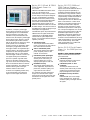
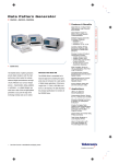
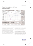
3066 • 3086
R e a l -Ti m e S p e c t r u m A n a ly z e r s
Features and Benefits
Seamless Acquisition for Capture of
Short Duration or Intermittent Events
Analyzes in Frequency, Time and
Modulation Domain
Applications
1st, 2nd, and 3rd Generation
Cellular/PCS R&D – Including GSM,
CDMA, IS-136, PDC, W-CDMA
Signature Analysis
DC to 3 GHz Coverage
Spectrum Monitoring
Frequency Event Trigger for Acquisition
of Burst or Infrequently Occurring
Signals
Settling Time Measurements for
Oscillators and Synthesizers
Post Capture 1000:1 Zoom Allows
Analysis of Individual Signals After
Wideband Capture
Debugging of Hardware/Software
Interface Problems
Phase Hit Capture and Measurement
Code Domain Power and
Complementary Cumulative Distribution
Function (CCDF) for IS-95, W-CDMA
Signals
CCDF for Multi-carrier and W-CDMA
Signals
The 3066 and 3086 are DC to 3 GHz real-time spectrum analyzers that allow the seamless capture of
frequency spectra with spans up to 30 MHz
(5 MHz – 3066). This allows the spectrum of burst
signals, such as those from GSM, IS-136, PDC or partial rate CDMA mobile stations, to be easily captured
and examined. Real-time spectrum analyzers take a
very different approach compared to traditional
sweeping spectrum analyzers. Rather than acquiring
one frequency step at a time, the real-time instrument
captures a block of frequencies all at once. Because
the instrument samples these full frames constantly
(rather than waiting for each discrete frequency step
to be measured), the signal can come or go as it
pleases and the real-time spectrum analyzer will
detect the change instantly.
The 12.1 in. color TFT display allows easy viewing
of spectrum, waterfall displays, spectrograms and
digital modulation analysis screens. Constellation
and vector diagrams can be displayed, as well as
frequency, phase, magnitude, I and Q versus time,
for in-depth analysis of digitally modulated signals.
Users can move a marker through the time record
and analyze the modulation at any point. In
particular, signals with symbol rates up to
20.48 Msymbols/sec (3066 – 5.3 Msymbols/sec) may
be analyzed during and after capture. This facilitates
analysis of W-CDMA signals with chip rates up to
16.384 Mcps.
®
Option 16: IS-95 and W- CDMA
Code Domain Power for
the 3086
3086
In addition, a frequency mask trigger
allows capture of randomly occurring or
infrequent signals such as intermittent
spurious emissions. If the user is not
interested in the period between transmission bursts, the frequency mask trigger
allows capture of the “burst-on” periods,
thus maximizing the number of bursts
that can be captured in memory for subsequent spectral, time or modulation
analysis. The user can graphically define
the frequency trigger mask; this allows
the trigger condition to be generated by a
particular event in the frequency domain
irrespective of other activity within the
displayed span. This is a major benefit
when the trigger condition is used to capture signals arising from intermittent
spurious or spectral re-growth events.
Option 1S, automatic waveform recording, can be used to store multiple memory
blocks to the internal hard drive without
operator intervention. This enables unattended monitoring and recording of
transient events for later review.
A 1000:1 zoom capability permits analysis to be performed on an individual
signal in a multi-signal environment.
2
CDMA and W-CDMA Base Station developers use code domain power
measurements to verify correct operation
of their designs. BTS amplifier designers
rely upon Complementary Cumulative
Distribution Functions (CCDF) to verify
the input and output amplitude distributions of their test waveforms. When
equipped with options 16 and 20, the
3086 now meets these needs for IS-95 and
W-CDMA designs. The real-time nature of
the 3086 spectrum analyzer brings unique
advantages to this application.
The 3086 with option 16 processes the WCDMA down-link signals as defined in
“Specifications for W-CDMA Mobile
Communication System Experiment
Version 1.1” and offers extensive analysis
capability including:
Code-domain power
The analyzer measures the relative
power to total power for each channel
with 1024 channels maximum
Time vs. code-domain power
The analyzer measures the relative
power at symbol points for each
channel as a time series
Code-domain power spectrogram
The analyzer measures the codedomain power continuously for
maximum 160 slots (0.1 s) and
displays spectrogram for each slot
Modulation accuracy
The analyzer measures EVM (error
vector magnitude), amplitude error,
phase error, waveform quality, and
origin offset for each channel
For customers who need code domain
analysis of IS-95 base station signals,
option 16 also provides code power measurements for IS-95 signals over a 6144
symbol period.
3066
•
3086
Option 20 CCDF (3066 and
3086) Feature Summary
Option 20 records the statistical nature of
a signal, and plots the probability of
exceeding a measured average value for
the waveform. A large amount of data is
collected in the memory of the 3086, and
Complementary Cumulative Distribution
Function (CCDF) can be shown over
selected periods of time to determine the
effect of code selection or multi-carrier
additions on the peak-to-average ratio of
the waveform. Base station amplifier
designers use this information to judge
the distortion performance of their products. The rapid changes that occur in base
station power outputs require a real-time
bandwidth higher than the occupied
bandwidth of the signals measured. The
3086 provides unique capability due to
its 30 MHz real-time bandwidth, allowing
CCDF measurements on up to 6 W-CDMA
carriers simultaneously. In the 3066,
CCDF measurements over a 5 MHz realtime bandwidth is possible.
Option 15: IS-95 Code Domain
Power for the 3066 Spectrum
Analyzer
OPTION 15 (3066) FEATURE SUMMARY:
Option 15 offers the measurement functions listed below:
Code-domain power
Measures the relative code power to
total power for each channel
Code-domain power vs. Time
(codegram)
The analyzer measures the codedomain power continuously for 6144
symbols (0.32 s) maximum and displays spectrogram for each symbol
Modulation accuracy and vector
display
Measures EVM (error vector magnitude), amplitude error, phase error,
waveform quality, and origin offset for
all signals
REAL-TIME
SPECTRUM
A N A LY Z E R S
Characteristics
INPUT/MEMORY MODE RELATED
Input Mode – RF, Baseband; Wideband,
IQ (3086 only).
Input Connector – N type (RF, Baseband,
Wideband), BNC type (IQ).
Input Impedance – 50 Ω.
VSWR (N type) – 1.5 (Reference Level
≥-20 dBm).
Acquisition Mode – Roll, Block.
Acquisition Memory Size – 16 Mbytes.
Acquisition Memory Management –
RF, Baseband Input.
Memory Mode: Frequency, Dual, Zoom.
FFT Points: 1024, 256 (Frequency Mode).
FFT Window: Rectangular, Hamming,
Blackman-Harris.
Block Size:
1 to 16,000 Frames (Frequency Mode, 256 pt).
1 to 4,000 Frames (Frequency Mode, 1024 pt).
1 to 2,000 Frames (Dual, Zoom Mode).
BASEBAND INPUT RELATED
Minimum Frame Update Time:
20 µs (Frequency Mode, 256 pt).
80 µs (Frequency Mode, 1024 pt).
160 µs (Dual, Zoom Mode).
Wideband, IQ Input (3086 only) –
Memory Mode: Zoom.
FFT Points: 1024.
FFT Window: Rectangular, Hamming,
Blackman-Harris.
Block Size: 1 to 2,000 Frames.
Minimum Frame: 25 µs.
F r e q u e n c y Sta n d a r d R e l at e d
Characteristic
Reference frequency
Initial frequency tolerance
Frequency stability
Aging
Temperature
Description
10 MHz
± 0.1 ppm
±0.0005 ppm/day
±0.002 ppm (5 to 40°C)
RF INPUT RELATED
Frequency –
Range: 10 MHz to 3 GHz.
Center Frequency Settability: 0.1 Hz.
Span: 100 Hz to 3 GHz.
Vector Span: 100 Hz to 6 MHz.
Real-time Span: 100 Hz to 5 MHz.
Number of Bins:
641 (100 Hz to 2 MHz span).
801 (5 MHz span).
481 (6 MHz span).
Span/6250 + 1 (span ≥ 10 MHz).
Spectrum Purity: –100 dBc/Hz (1 GHz CF,
200 kHz span, 0 dBm ref, 10 kHz offset).
Residual FM: 3 Hz p-p.
3066
•
3086
REAL-TIME
Amplitude –
Reference Level: –50 dBm to +30 dBm.
Maximum Nondestructive Input Power: +30 dBm.
Self Gain-Calibration Accuracy: ±1.0 dB at
25 MHz within 5°C temperature variation.
Flatness: ±2.0 dB (10 MHz to 3 GHz).
Input Equivalent Noise: –140 dBm/Hz.
3rd Order Distortion: –65 dBc (–10 dBfs input, at
1 GHz).
Residual Response: –70 dBfs (0 dBm ref, 5 MHz
span).
Image Suppression: 70 dB.
Spurious Free Dynamic Range (1 GHz CF, 0 dBm
REF, sinusoidal signal at the center, spur apart
more than 10 kHz from the signal):
80 dB at 50 kHz span.
75 dB at 100 kHz span.
70 dB at 200 kHz and 500 kHz span.
65 dB at 1/2/5 MHz span.
Frequency –
Range: DC to 10 MHz.
Center Frequency Settability: 0.1 Hz.
Span: 100 Hz to 10 MHz.
Vector Span: 100 Hz to 6 MHz.
Real-time Span: 100 Hz to 5 MHz.
Number of Bins:
641 (100 Hz to 2 MHz span).
801 (5 MHz and 10 MHz span).
481 (6 MHz span).
Spectrum Purity: –100 dBc/Hz (5 MHz CF,
200 kHz span, 0 dBm ref, 10 kHz offset).
Residual FM: 2 Hz p-p.
Amplitude –
Reference Level: –30 dBm to +30 dBm.
Maximum Nondestructive Input Power: +30 dBm.
Reference Level Accuracy: ±0.5 dB at 5 MHz.
Flatness: ±1.0 dB (1 MHz to 10 MHz).
Input Equivalent Noise: –150 dBm/Hz.
2nd Harmonic Distortion: –70 dBc (at 4.5 MHz).
DC Offset: –40 dBfs.
Residual Response: –70 dBfs (5 MHz CF, 5 MHz
span, 0 dBm ref).
Alias Suppression: 65 dB.
Spurious Free Dynamic Range (5 MHz CF, 0 dBm
ref, sinusoidal signal at the center, spur apart
more than 10 kHz from the signal):
85 dB at 50 kHz span.
80 dB at 100 kHz span.
75 dB at 200 kHz span.
70 dB at 500 kHz span.
70 dB at 1/2/5 MHz span.
SPECTRUM
A N A LY Z E R S
WIDEBAND INPUT RELATED
(3086 ONLY)
Frequency –
Range: 50 MHz to 3 GHz.
Center Frequency Settability: 0.1 Hz.
Span: 10 MHz, 20 MHz, 30 MHz.
Vector Span: 10 MHz, 20 MHz, 30 MHz.
Number of Bins:
501 (10 MHz and 20 MHz span).
751 (30 MHz span).
Amplitude –
Reference Level: –50 dBm to +30 dBm.
Maximum Nondestructive Input Power: +30 dBm.
Flatness within Span: ±1 dB (25°C ±5°C).
Input Equivalent Noise: –140 dBm/Hz.
3rd Order Distortion: –65 dBc (–10 dBfs input, at
1 GHz).
Residual Response: –60 dBfs (0 dBm ref, 30 MHz
span).
Image Suppression: 70 dB.
Spurious Free Dynamic Range (1 GHz CF, 0 dBm
ref, sinusoidal signal at the center, spur apart
more than 500 kHz from the signal):
65 dB at 10 MHz span.
60 dB at 20 MHz and 30 MHz span.
IQ INPUT RELATED (3086 ONLY)
Frequency –
Range: ±15 MHz.
Span: 10 MHz, 20 MHz, 30 MHz.
Vector Span: 10 MHz, 20 MHz, 30 MHz.
Number of Bins:
501 (10 MHz and 20 MHz span).
751 (30 MHz span).
Amplitude –
Reference Level: 100 mV (amplitude of IQ signal).
Maximum Nondestructive Input Power: ±5 V.
Flatness within Span: ±0.5 dB (25°C ±5°C).
Residual Response: –60 dBfs (30 MHz span).
Alias Suppression: 55 dB.
Spurious free dynamic range (1 GHz CF, 0 dBm
ref, sinusoidal signal at the center, spur apart
more than 500 kHz from the signal):
65 dB at 10 MHz span.
60 dB at 20 MHz and 30 MHz span.
3
Characteristics
FRAME TIME RELATED
M i n i m u m F r a m e U p d at e Ti m e
TRIGGER RELATED
F r a m e Ti m e ( 3 0 8 6 )
Span
Trigger Mode – Auto, Normal, Quick, Delayed,
Interval, Quick-interval, Timeout, Auto, Normal
[RF (span ≤ 6 MHz) and Baseband Input,
Wideband and IQ Input (3086 only)].
Trigger Source – Internal/External.
Trigger Domain – Frequency, Time.
Trigger Position – 0 to 100%.
Frequency Trigger Mask –
Frequency Resolution: 1 bin.
Trigger Level Range: 0 dBfs to –70 dBfs.
Time Trigger Mask –
Time Resolution: 1 data point.
Trigger Level Range: 0 dBfs to –40 dBfs.
External Trigger Threshold Level – 1.6 V.
Span
1024 point
Baseband Mode:
10 MHz
80 µs
RF Mode and Baseband Mode:
6 MHz
80 µs
5 MHz
160 µs
2 MHz
320 µs
1 MHz
640 µs
500 kHz
1280 µs
200 kHz
3200 µs
100 kHz
6.4 ms
50 kHz
12.8 ms
20 kHz
32 ms
10 kHz
64 ms
5 kHz
128 ms
2 kHz
320 ms
1 kHz
640 ms
500 Hz
1280 ms
200 Hz
3200 ms
100 Hz
6400 ms
Wideband/IQ Input Modes: 3086 Only
30 MHz
25 µs
20 MHz
25 µs
10 MHz
50 µs
4
256 point
20 µs
20 µs
40 µs
80 µs
160 µs
320 µs
800 µs
1.6 ms
3.2 ms
8 ms
16 ms
32 ms
80 ms
160 ms
320 ms
800 ms
1600 ms
25 µs
25 µs
50 µs
1024 point
256 point
FFT
FFT
Baseband/Frequency Mode
10 MHz
80 µs
20 µs
RF/Baseband/Frequency Mode
500 kHz to 6 MHz
80 µs
20 µs
50 kHz to 500 kHz
200 µs
50 µs
5 kHz to 20 kHz
2000 µs
500 µs
500 Hz to 2 kHz
20 ms
5 ms
200 Hz
50 ms
12.5 ms
100 Hz
100 ms
25 ms
RF/Baseband/Dual Mode
500 kHz to 6 MHz
160 µs
N/A
50 kHz to 500 kHz
400 µs
N/A
5 kHz to 20 kHz
4 ms
N/A
500 Hz to 2 kHz
40 ms
N/A
200 Hz
100 ms
N/A
100 Hz
200 ms
N/A
RF/Baseband/Zoom Modes
5 MHz
160 µs
N/A
2 MHz
320 µs
N/A
1 MHz
640 µs
N/A
500 kHz
1.28 ms
N/A
200 kHz
3.2 ms
N/A
100 kHz
6.4 ms
N/A
50 kHz
12.8 ms
N/A
20 kHz
32 ms
N/A
10 kHz
64 ms
N/A
5 kHz
128 ms
N/A
2 kHz
320 ms
N/A
1 kHz
640 ms
N/A
500 Hz
1280 ms
N/A
200 Hz
3200 ms
N/A
100 Hz
6400 ms
N/A
Wideband/IQ Input Modes – 3086 Only
30 MHz
25 µs
N/A
20 MHz
25 µs
N/A
10 MHz
50 µs
N/A
3066
•
3086
DISPLAY/VIEW
Data Display –
Waveform:
Frequency vs. Amplitude/Phase.
Frequency vs. I/Q voltage.
Time vs. Amplitude/Phase.
Time vs. I/Q voltage.
Spectrogram: Time vs. Frequency vs.
Amplitude/Phase.
Waterfall:
Time vs. Frequency vs. Amplitude/Phase.
Time vs. Frequency vs. I/Q Voltage.
Time vs. Amplitude/Phase Multi-Frame.
Time vs. I/Q Voltage Multi-Frame.
AM Demodulation: Time vs. Modulation depth.
FM Demodulation: Time vs. Frequency deviation.
PM Demodulation: Time vs. Phase deviation.
FSK Demodulation: Time vs. Frequency deviation.
Polar: Vector diagram, Constellation diagram.
Eye Pattern: I, Q, Trellis.
Symbol Table: Binary, Octal, Hexadecimal.
Error Vector: EVM, Magnitude error, Phase error,
Waveform quality (ρ).
View –
Number of Views: 1, 2, 4.
Settable Views: 8 maximum.
Display Traces: 2 on waveform display.
LCD Panel –
Size: 12.1 inch.
Display Resolution: 1024 x 768 pixels.
Color: 256 color (maximum).
REAL-TIME
SPECTRUM
A N A LY Z E R S
Characteristics
DIGITAL DEMODULATION RELATED
EMC COMPLIANCE
D i g i ta l D e m o d u l at i o n R e l at e d
Characteristic
Demodulator
Carrier type
Modulation format
Measurement filter
Reference filter
Filter parameter
Maximum symbol rate
Standard setup
Display format
Vector diagram
Constellation diagram
Eye diagram
Error vector diagram
Symbol table
Error measurement accuracy
PDC
PHS
GSM
IS-95 reverse link
QPSK, 4.096 Msps, 2 GHz
QPSK, 16.384 Msps, 2 GHz
Description
Continuous, Burst
BPSK, QPSK, π/4 Shift DQPSK, 8PSK, OQPSK, 16QAM, 64QAM, GMSK
Root Cosine
Cosine, Gauss
α/BT: 0.0001 to 1, 0.0001 step
5.3 Msps (RF, Baseband); 20.48 Msps (Wideband, IQ; the 3086 only)
PDC, PHS, NADC, TETRA, GSM, CDPD, IS-95, T-53
Symbol/locus display, Frequency error measurement, Origin offset measurement
Symbol display, Frequency error measurement, Origin offset measurement
I/Q/Trellis display (1 to 16 symbols)
EVM, Magnitude error, Phase error, Waveform quality (ρ) measurement
Binary, Octal, Hexadecimal
10 frames averaged
EVM <1.2%, Mag error <1.0%, Phase error <0.8° (100 kHz span)
EVM <1.4%, Mag error <1.2%, Phase error <0.8° (1 MHz span)
EVM <1.8%, Mag error <1.2%, Phase error <1.0° (1 MHz span)
EVM <2.0% (5 MHz span)
EVM <2.5% (20 MHz span)
EVM <3.0% (30 MHz span, 25°C ±5°C)
MARKER ZOOM RELATED
ENVIRONMENTAL
Marker –
Marker Type: Normal, Delta, Band-Power.
Search Function: Peak Right, Peak Left, Maximum.
Link between Views: On/Off.
Measurement Function – Noise Power, Power
within Band, C/N, Adjacent Channel Power,
Occupied Bandwidth.
Digital Zoom –
Zoom Ratio: 2 to 1000.
Maximum Span in the Zoom Mode: 5 MHz
(RF, Baseband), 30 MHz (Wideband, IQ, 3086
only).
Temperature Range –
Operating: +5 to +40°C (floppy not used), +10 to
+40°C (floppy used).
Nonoperating: –20 to +60°C.
Humidity – Operating and nonoperating: 80%
non-condensing. Maximum wet-bulb temperature 29°C.
Altitude –
Operating: Up to 2,000 m (6,500 ft).
Nonoperating: Up to 12,000 m (40,000 ft).
Random Vibration –
Operating: 0.27 g, 5 to 500 Hz, 10 minutes each
axis.
Nonoperating: 2.28 g, 5 to 500 Hz, 10 minutes
each axis.
Shock – Nonoperating: 20 g half-sine, 11 ms
duration, 3 shocks per axis in each direction
(18 shocks total).
Package Product –
Vibration and Bounce: Meets ASTM D999-75,
Method A, Para. 3.1g, (NSTA proj. 1-A-B-1).
Drop: Meets ASTM D775-61, Method 1, Para. 5,
(NSTA proj. 1-A-B-2).
SYSTEM CONTROLLER
Pentium MMX 200 MHz, 64 Mbyte SIMM,
Windows 95, PCI, ISA, TMP68301 16 MHz,
2.1 Gbyte 3.5 inch EIDE, 1.44 Mbyte floppy drive,
GPIB IEEE488.1, Keyboard PC/AT. (order
separately), Centronics parallel port, SCSI 2.
3066
•
3086
REAL-TIME
SPECTRUM
A N A LY Z E R S
Emissions –
Enclosure: EN55011 Class A, limits for radiated
emissions.
AC Main: EN61000-3-2 Power line harmonics;
EN55011 Class A, limits for radiated emissions.
Immunity –
Enclosure: EN61000-4-2 ESD (Up to 8 kV, 150 pF
through 330 Ω) Internal terminals of connectors
do not allow ESD test.
AC Main: EN61000-4-3 Radiation; EN61000-4-4
Fast Transient Burst; EN61000-4-5 Surge;
EN61000-4-6 Conductive Immunity.
SAFETY
Safety – UL3111-1, CSA231, EN61010-1,
IEC61010-1.
POWER
Line Voltage – 100 to 240 VAC Nominal.
Line Frequency – 47 Hz to 66 Hz.
Line Fuse – 10 A, fast.
Primary Circuit Dielectric Voltage
Withstand Grounding Impedance –
1,500 Vrms, 50 Hz for 15 s, without breakdown.
Verify continuity of grounding connection, by any
suitable means, between a representative part
required to be grounding and attachment– plug
cap grounding pin. (0.1 Ω at 30 A).
Maximum Power – 280 W.
Maximum Line Current – 3.0 A rms at 50 Hz.
Surge Current – 15 A at 100 VAC; 30 A at
200 VAC.
Physical Characteristics
Dimensions
Height
Width
Depth
Weight
Net
mm
270
430
600
kg
28
in
10.6
16.9
23.6
lb
62
WARRANTY
One year parts and labor.
5
Ordering Information
3086
Real-time Spectrum Analyzer.
Includes: User Manual, U.S. Power Cord, mouse.
3086 OPTIONS
Opt. 1S – Data capture software.
Opt. 16 – W-CDMA and IS-95 Code Domain Power
for 3086.
Opt. 20 – CCDF measurements for 3086.
3066
Real-time Spectrum Analyzer.
Includes: User Manual, U.S. Power Cord.
3066 OPTIONS
Opt. 1S – Data capture software.
Opt. 15 – IS-95 Code Domain Power for 3066.
Opt. 20 – CCDF for 3066.
6
MEASUREMENT SERVICE OPTIONS
Opt. C3 – Three years of calibration services.
Opt. C5 – Five years of calibration services.
Opt. D1 – Test Data.
Opt. D3 – Test data (requires Opt. C3).
Opt. D5 – Test data (requires Opt. C5).
Opt. R3 – Three years of repair protection.
Opt. R5 – Five years of repair protection.
INTERNATIONAL POWER OPTIONS
Opt. A1 – Universal Euro 220 V, 50 Hz.
Opt. A2 – United Kingdom 240 V, 50 Hz.
Opt. A3 – Australian 240 V, 50 Hz.
Opt. A4 – North American 240 V, 60 Hz.
Opt. A5 – Switzerland 220 V, 50 Hz.
3066
•
3086
RECOMMENDED ACCESSORIES
PC Display Analysis Software (3066) – Order
SL7PC66.
SL7PC66 Opt. 15 – IS-95 Code Domain Power for
SL7PC66.
SL7PC66 Opt. 20 – CCDF for SL7PC66.
PC Display Analysis Software (3086) – Order
SL7PC86.
SL7PC86 Opt. 16 – W-CDMA IS-95 Code Domain
Power for SL7PC86.
SL7PC86 Opt. 20 – CCDF for SL7PC86.
REAL-TIME
SPECTRUM
A N A LY Z E R S
3066
•
3086
REAL-TIME
SPECTRUM
A N A LY Z E R S
7
For further information, contact Tektronix:
Worldwide Web: for the most up-to-date product information visit our web site at: www.tektronix.com/Measurement/commtest/
ASEAN Countries (65) 356-3900; Australia & New Zealand 61 (2) 9888-0100; Austria, Central Eastern Europe, Greece, Turkey, Malta,& Cyprus +43 2236 8092 0;
Belgium +32 (2) 715 89 70; Brazil and South America 55 (11) 3741-8360; Canada 1 (800) 661-5625; Denmark +45 (44) 850 700; Finland +358 (9) 4783 400;
France & North Africa +33 1 69 86 81 81; Germany + 49 (221) 94 77 400; Hong Kong (852) 2585-6688; India (91) 80-2275577; Italy +39 (2) 25086 501;
Japan (Sony/Tektronix Corporation) 81 (3) 3448-3111; Mexico, Central America, & Caribbean 52 (5) 666-6333; The Netherlands +31 23 56 95555; Norway +47 22 07 07 00;
People’s Republic of China 86 (10) 6235 1230; Republic of Korea 82 (2) 528-5299; South Africa (27 11)651-5222; Spain & Portugal +34 91 372 6000;
Sweden +46 8 477 65 00; Switzerland +41 (41) 729 36 40; Taiwan 886 (2) 2722-9622; United Kingdom & Eire +44 (0)1344 392000; USA 1 (800) 426-2200.
From other areas, contact: Tektronix, Inc. Export Sales, P.O. Box 500, M/S 50-255, Beaverton, Oregon 97077-0001, USA 1 (503) 627-6877.
Copyright © 2000, Tektronix, Inc. All rights reserved. Tektronix products are covered by U.S. and foreign patents, issued and pending.
Information in this publication supersedes that in all previously published material. Specification and price change privileges reserved.
TEKTRONIX and TEK are registered trademarks of Tektronix, Inc. All other trade names referenced are the service marks,
trademarks or registered trademarks of their respective companies.
2/00
HB/XBS
2EW-12989-1