1
Dens digital simulating system *
by H. POTASH, A. TYRRILL, D. ALLEN,
S. JOSEPH, and G. ESTRIN
Universiity of California
Los Angeles, California
INTRODUCTION-SIMULATION SYSTEMS
1. A set of basic building blocks whose properties
are known is available.
2. An instruction set or task assignment for the
computer system is defined along with cost and
performance constraints.
3. Using his experience and intuition, the designer
generates an ensemble of modules. These modules form the system's building blocks which the
designer believes will perform the stated functions effectively.
To see a world in a grain of sand
And a heaven in a wild flower,
Hold infinity in the palm of your hand
And eternity in an hour.
-William Blake
This article is concerned with the problems of digital
simulation and describes methods used in the Digital
Control Design System (DCDS)1 for the simulation
of digital structures. The paper is divided, into five
parts:
• A short introduction to DCDS, its structure and
purposes.
Given the above (1-3), the digital system must
be describable to a design aid system. The designer
then needs a language, its translator, and an operating
system with the following properties:
4. The set of functions to. be performed can be
described.
5. The building blocks, their interconnection, and
their place and function within the ensemble
can be described.
6. A computer program can generate a fabrication
description of control modules capable of going
through a sequence of states necessary to have
the system perform the above functions. The
designer may specify synchronous or asynchronous control systems.
7. A simulator can accept the descriptions in (4)
and (5), and the sequence description generated
in (6), and produce measures of accuracy and
performance.
8. If the performance of the ensemble is "good",
the description of the computer. system is in
such form that. it may be fed into a more de-
• A discussion of simulation techniques, entities and
attributes.
• The DCDS pseudo machine simulator.
• The pseudo machine program.
• A simple example'of a DCDL program.
DeDS, its structure and purposes
The Digital Control Design System (DCDS) was
developed at the University of California at Los
Angeles to aid in the design and architecture of computer systems. The design system operates under the
following assumptions:
• This refj~arch was supported in part by the Atomic Energy
AT(ll-l) Gen 10 Project 14, and the Office.of Naval
Research, Information Systems Branch, NOOO14-67-A-0111-0016.
Commi~eiG)n
707
From the collection of the Computer History Museum (www.computerhistory.org)
708
Fall Joint Computer Conference, 1969
----------------------------------------,--tailed design process. If l1ot, the designer may
al ter his architecture.
To satisfy the above needs, Digital Control Design
Language (DCDL) has been implemented as part- of
design automation research being conducted at the
University of California at Los Angeles. 2- 6 A. compiler
for DCDL has been implemented for the SSD SIGMA
7 using a META 5 compiler writing systcm. 6 ,7 The
DCDL compiler is currently also being implemented
for the IBM/360.
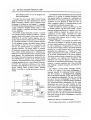
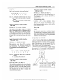
The DCDL system illustrated in Figure 1 contains
two compiler processors written in META 5, a pseudo
machine (which is the subject oithis paper) written in
FORTRAN IV and the machine language, and twO"
control implementation modules written in FORTRAN
IV. T~e input processor is a DC:r;>L syntactic analyzer;
(~) thIS program translates the digital system descriptIOn (example in Part IV) into an interpretive code
used by the pseudo-machine for simulation of the
described hardware. The second META 5 processor
(2) produces a numerical code which is then transformed
into a binary control program and a fabrication description of a control subsystem for the computer system
being designed. The implementation specificatio~s for
the wiring of the control matrices are produced by the
two FORTRAN IV programs (3,4). Control modules
imp~ied by microprograms have their wiring lists automatICally generated by the Control Matrix Processors
in DCDS. The hardware construction of the controi
processor is then effected by using a set of one or more
similar building blocks (Control Matrix Building
Blocks), according to wiring specifications given by
DCDS.
The software module described in Part III is a pseudo
machine {5) in charge of executing simulation runs.
The pseudo machine is composed of a combination of
FORTRAN IV and machine language subroutines. The
simulation runs are designed to check test cases in
order to ass~ss the validity of a described design as well
as to calculate its estima.ted execution time.
DCDS is designed to analyze asynchronous as well
as clocked systems, with the former posing a. spedal
problem: dynamic reevaluation of variables. Any time
a logical variable is changed, the system must, as a
consequence of this change, reevaluate any other
variable which is a function of the changed variable.
This process must continue until no further "consequential changes" occur.
DCDS's capability to dynamically reevalua,te vari_abIes allows the designer to describe his system using
-the same logical equations and timing relations which
he uses to implement it. Programming in a form (see
Part IV) which is highly related to the actual hardw:are
provides for a system directly used by the designer
eliminating the programmer as a "middle-man". This
direct correspondence also makes the DCDL progr:am
an up-to-date documentation of the system designed.
The syntax analyzer accepts a description which images
the hardware and translates this description into
simulation code. Thus the designer is freed from the
tedious job of programming the structure-of the model
required-a process sometimes more time-consuming
than building a hardware prototype and testing it on
the bench.
'rhe Digital Control Design Lang~ge (DCDL)
is built as a ~luster of three ntain sublanguages: a
language intended for expressing ~~olean €:guations
and time relations; a microprogramming language;
and an algorithmic language. DCDL uses FORTRAN
as the algorithmic sublanguage. The user may choose
anyone of the three sublanguages to describe any of
the parts or module"s in the describ~d design. The logical
aI).d micl'oprogrammi'nlg sublangu~g~s use the s~me
declarations and access the same variables by their
names. The execution statements of sublanguages a.nd
their syntactic formats differ and one cannot combine
statements of different sublangu,ages. Thus DCDS
~rovides' the user with a powedul means of expression,
since he can select the most convenient and expressive
form from among the three s'ublanguages to describe
a hardware module.
Entities and attributes in simulation systems
Figure I-DCDS system flow chart.
For our observations herein, we consider the simula-
From the collection of the Computer History Museum (www.computerhistory.org)
DGDS
Digital
Simulating System
.
(
709
1,
tion of a ~ystem to be the modeling and associated
measurement of a system by a STRUCTURE in which
EVENTS occur in TIME according to a set of RULES.
Thus there are four sets of basic elements which must
be dealt with in simulation:
The input to circuit analysis programs like NASAP
and LISA or to the Boolean Analyzer is in table-form
which either explicitly gives the set of rules (Boolean
equations) 01' gives a table that implies a unique set
of rules (Kirchoff's and Ohm's equations for the circuit).
STRUCTURES, EVENTS, TIMES, and RULES
Main Entities-8TRUCTURES
Different simulation methods neglect one or more of
these sets (e.g., time independent models). Anyone of
the four sets may be selected as primary entities and
the others treated as attributes of that set.
One may choose to consider an analytic closed form
solution to be a simulation of a real system. In this
case, the process of simulation becomes a transformation. ~ssume for examQle the transfer equation for an
electronic circuit. Both internal even.ts (voltages and
currents in the individual elements) and struct?J,re
(top~logy of the circuit) may be neglected and one
manipulates the set of rules (Le. Kirchoff's law and
Ohm's equatiqns) to produce a transfer function which
gives the output event~ as a function of time and ~nput
events.
Thus whenever the rules are considered to be the
main entities, then either an analytic transformation or
an algorithmic procedure is used for simulation. The
type and form of the information transferred into the
simulation system as well as the simulation systems
themselves vary from one another depending upon
~hich of the four sets was chosen as the main. set of
entities. Due to these differences, different languages
or input rules are used to describe the simulated system
to the software package designed to perform the simulation.
The following examples of different programming
structures will serve to illustrate the previous discussion.
Main Entities-EVENTS
Examples of programming structures:
SIMULA [8], GASP [9], SIMSCRIPT [10], [11],
[1~], [13], GPSS [14].
A simulated system is described by an event flow
chart. The programming systems above use input
~anguage formats suitable for the description of events
in such a form.
Main Entities-RULES
Examples:
NASAP [15], LISA r16], Boolean Analyzer [17].
Examples:
LOGIK
[1~],
Weather Simulation Program [19].
Partial Differential Equation Simulation [20].
The input format is any form suitable for describing
the physical or hierarchical structure of the simulated
system.
Modeling and approxima,tions
After the selection of the entity and attribute relations, the next step for simulating a system is to decide
what can be approximated and how the selected approximations c~p. be done. The choice of what to approximate can be categorized as:
a. mak~g certain entities (inputs) constants; for
example t = 0 in time independent mo~eling.
h. neglecting parts of the attributes; for example
in simulation of partial differential equations by
Monte Carlo methods, the field constants are
calculated for only a small number of selected
field points in the structure.
c. modifying the set of rules; the use of differenc~
equations to solve partial differential equation
problems is an example of modifying the rules,.
For a different example of rule modification,
consider a simulation program simulating another program on a digital system. The purpose
of the simulated program is to execute a matrix
inversion in which the inversion is performed
on a 2X2 part o{the matrix instead of the entire
n X n array. In this case, the system rules may be
modified to obtain fast simulation time for a
simualtion that "takes the system through the
motions" without obtaining the actual numerical result. Thus for Such approximatiop.s,
one ~ay simulate the system faster than real
run time.
Event directed simulation can be expected to be faster
than structural simulation since structure simulation
has to go through all possible events in the system,
while event simulation takes the system only through
From the collection of the Computer History Museum (www.computerhistory.org)
710, Fall Joint Computer Cqnference, 1969
--------------------------------------------------------------------------------------,-----the prescribed events. This is, of course, also the main
pitfall of event simulation; it does' not point out events
that might occur in the system but are unforeseen by
the programmer.
struction in the program stack) transfer of data 1~0
register A. All the other consequences of this action
(i.e., all the outputs of gates whose input is A) are
simulated from the Call Stack (structure simulation.).
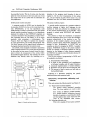
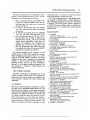
DCDS pseudo machine simulator
The pseudo machine program
A computer module in DCD L may be described by
its structure (LOGIC), by the set :of events that it controls (PROGRAM), or by th~ algorithmic rules
(SIMULATE). In order to perforrrt this task, the DCDS
pseudo machine simulator operates as an algorithmic
simulator by calling on the FORTRAN programs; as
a structure simulator when simulating a logical structure (operating from the Call Stack); or as an event
simulator when processing a microprogram. The
Program Stack (see Figure 2) operates the sequence
of events generated by the control microprogram. The
Call Stack operates all the logical details occurring in
the logical structures forced by the control events.
The DCDL event simulation is limited to operations
within a logical structure. The eve~ts that are generated
by the control as time moves forward, forces the simulator to follow all consequences of the events within
the described logical structure. For example, the event
simulator may directly order (by executing an in-
A pseudo machine processor is a program written in
machine language or higher level language for the
machine on which one performs the simulation runs.
In the present implementation on the SIGMA 7 this
program is written using FORTRAN and aBsembly
language.
The process in which the translation is separated
from the simulation allows one to write the translator
program independently of the machine in use. The
separation of the compiler program and the pseudo
machine program allows independent debugging and
changes in each. Modifications in DCDL tmd i1GS
compiler are done by changing the META 5 compiler
program. FORTRAN changes in the pseudo machine
provide for changes in simulation methods as well as
insertion by the designer of other features expressed
in FORTRAN to capture event information relevant to
one design or another.
Thus, by the process of programming in DCDL and
by translation one obtains:
INOEXING ANO
ARITHMETIC UNIT
IMCI
INSTRUCTION REGISTER
ANOCOUNTER
A. Documentation of the design;
B. A check on the consistency and completene8s
of all logical variables and all logical functions;
C. Automatic implementation of control sections;
D. Simulation runs for given sets of input data; and
E. The amount of time a certain run will take on
the described design.
Following is a discussion specifying the pseud.o
machine structure and operation codes.
Instructions, interpretation, addressing, and
indexing
OR
PROGRAM
STACK
This unit contains the following parts (see Fi~~ure 2).
(a) Time counter and time registers.
The counter counts simulated execution
time. The time registers are u,ed to store
REGULAR
LOGICAL
VARIABLES
TEMPORARY
LOGICAL
VARIABLES
OELAYEO
STORAGE
TABLE
ARITHMETIC
VARIABLES
INSTRUCTION
TABLE
MEMORY
Figure 2-Pseudo machine structure
time counts of different parallel br,anches.
At a parallel junction, comparison between
duration of operation on each branch is made
and the highest time count will be the new
value of the simulation time counter.
(b) Indexing arithmetic unit.
This unit is capable of fixed point operatioJ[l
From the collection of the Computer History Museum (www.computerhistory.org)
DCDS Digital Simulating System
(plus, minus, multiplication, and division)
and is used for indexing arithmetic.
(c) Call-stack and Program-stack.
Two push down (LIFO) stacks. One of the
elements in the stacks is the operative address; i.e., the address of the instruction to
be executed next. The operative address
is usually the word at the top of the callstack. If the call-stack is empty, the operative address is the word at the top of the
program -stack.
A control branch to a lower (subordinate)
control level (CALL) is instrumented by
putting the first address of the lower control
level program into the call stack, thus making
the call address the operative address. When
the lower control level is of type PROGRAM,
the address is put in the program stack.
The operative address is incremented by
1 after an instruction is executed or the
address is replaced by another due to the
execution of a branch (a normal branch that
occurs within the program being executed).
An exit or return from the subordinate program will
cause the stack to pop while a further entry into another
subordinate program brings a new address into the call
stack. The consequential calls are put into the call
stack but their execution is delayed until all the parallel
operations have been carried out and then all consequential calls are carried out. Two key words in DCDL
indicate parallel structures. *GROUP indicates a set
of similar modules operating in parallel and controlled
by the same binary control variable (for example,
a set of 32 single bit adder modules in a 32 bit binary
adder). *PART indicates a set of dissimilar modules
operating in parallel under the control of a single
binary control variable (for example, shifter and counter
in floating point normalization). A *PART may contain simple and nested *GROUPS in which case the
whole structure is operating simultaneoulsy under
the supervision of a single control variable. The stacks
have three points. TOPC (top of the call stack). TOPP
(top of the progranl stack) and OPR (the operative
address.)
OPR = TOPP.if call stack is empty
OPR = TOPC if call stack is not empty
OPR = TOpe at the time of entry to *GROUP
or *PART if executing inside a *GROUP
or a *PART.
711
Consequential calls are intended for the dynamic
reevaluation of variables. The STORE instruction
invoking the consequential calls puts new addresses
of variable reevaluation routines into the Call Stack.
This is accomplished according to the following steps:
1. The old and the new value of the variable are
compared.
2. The new variable value is stored.
3. If the comparison mentioned above shows a
difference between the old and new value, the
address of the subroutine that calculated the
new value of the dynamically dependent variable is put into the Call Stack.
4. The address of the next instruction is the address
on the top of the Call Stack. Thus, if there were
allY consequential calls, they would be executed
prior to the completion of the execution of the
subroutine that invoked those consequential
calls.
When there are no more changes in the values of the
variables, the instructions proceed to the end of the
reevaluation routine, which contains RETURN as
the last instruction. The RETURN instruction pops
the Call Stack sending the program to finish operations
in the routine which invoked the consequential calls.
The process of dynamic reevaluation will stop only
if the variable values and the logical functions are
consistent. Assume the following st~tements:
A = /\ (B,C);
D = V (A,E);
B = ~ D;
with initial conditions A = 0, B = 1, C = 0, D = 0,
E = O. This set of relations and values is consistent.
Now (lonsider that the variable C is changed to one. The
new set up of variables and relations is inconsistent
and the reevaluation of variables will not reach a
steady state. Each reevaluation will put a new address
in the call-stack:
A change in operation occurs once an address is
put into location n in the stack. The pseudo machine
prints an error message which is followed by the names
and values of variables partaking in a STORE instruction. This process continues allowing the program to
put addresses in the next ten slots of the call stack.
When the execution calls for storing an address at
n+ll the call stack is cleared (TOPC = 0) and the
operative address is tllken as the instruction on top
of the program stack. This debug feature allows the
From the collection of the Computer History Museum (www.computerhistory.org)
712
Fall Joint Computer Conference, 1969
----------------------------------------------------------------------_,----program .to check for IQgical inconsistencies without
getting into an infinite loop or having to stop simulalation runs.
5. Delay table. The result of a logical transformation specified in DCDL can be effected directly
or after a specified time, for example in the
statement
A
=
'DELAY(3)' & (C, D, E): OPl;
the transformation &(C, D, E) is performed if
control variable OP1 is activated, but the content of A will be changed only three time unitR
later.
To facilitate translation of the delay modifier, the
pseudo machine contains a delay table. An entry into
the delay table contains three parts: variable name
variable's new value, time of exit.
Variable name
Variable value
I
Exit
time
Each time the time counter is incremented, all time
of exit entries into the delay table are checked, and
the entries with a time of exit matching the time counter
activates a store operation storing the new value in
the appropriate variable, invoking consequential calls
if such are present.
Logical manipulating accumulators
The pseudo machine contains two string accumulators, A and B. The machine performs the operations
of AND, OR and EQUAL between the respective bits
of the string accumulators and the result is stored in
string accumulator A. The current size of both string
accumulators is given by the content of String Accumulator Size Register (SASR).
All operations are performed on words of the same
size. Calling an operand of the wrong size causes an
error message printout and the machine goes to the
next instruction. An exception to. this occurs when the
operand is of size one bit. In this case, the one bit is
extended to a word that contains all zeros or all ones
of the size indicated by the SASR. A special imltr~ction
sets the size of the string accumulator (Le., the cont£mt
of SASR) thus setting the size of all followin:g logi1cal
operations.
Data Blocks
Data blocks have different lengths and contli.in
binary arrays. A binary array can possess up to three
dimensions. Only a single bit or a binary word string
can be addressed in the blocks. Each data block contains a two word header containing the variable name
followed by the structure described below.
Storage for a Single Bit
The storage blcok for a single bit is one word (four
bytes) plus a word for each consequential call. A
consequential call occurs when a variable A is a dlynamic function of a variable B. B forms the input to
the gate, the output of which is A. When B is <,hanged,
a consequential call causes the pseudo-machine to
reevaluate the variable A. Thus, the storage location
of variable E contains the addresses of sets of instructions which will reevaluate all variables which are
dynamically dependent on the variable B.
The single bit storage words format
variable value
indicator flags
number of consequential calls
Byte 1: number of consequentilal calls
invoked by a change in the
stored binary variable.
Byte 2: this byte contains indicn.tors for
high bit position, number of
dimensions of th~ logical variable, and variable type. Eaeh
indicator occupies two bits.
From the collection of the Computer History Museum (www.computerhistory.org)
DCDS Digital Simulating System
1
Format:
2
variable dimension
00:
bit variable
01:
one dimension array (word)
10:
two dimensional variable
11:
three dimensional variable
I
I
3
713
4
variable
storage
cc directive
cc address
"
consequential
"
call
"
address
variable type
00:
logical point, the variable does not
contain memory
01 :
1 level storage, declared as *RS
10:
2 level storage (clocked)
position of the high order bit
00:
the high order bit is the roost significant bit
(leftroost bit)
01:
the high order bit is the least significant bit
(rightmost bit)
Byte 3: not used
Byte 4: variable value
The following words .(if any) contain the consequential
call address in byte 3 & 4 and its directive in byte 1.
Byte 1: consequential call type (directives)
011: calls on any change in the variable
001: consequential call, only if the variable
changes from 0 to 1
010: consequential call, on the change of the
variable from 1 to 0
First word: Byte 1: number of consequential calls
Byte 2: variable dimension, high order
bit position and variable type
(same as for bit storage)
Byte 3: lowest SUbscript of variable
Byte 4: size of varia.ble.
The second word through the nth word
1)
word size
n
=
---3;--contain the value of the binary
(
+
word. If the variable is a clocked F IF, the amount of
space for variable storage is doubled and each bit has
two storage locations, primary and secondary.
The last set of words contains consequential call
addresses and their directives.
Two dimensional binary storage
1
2
3
4
5
6
IIIII
IIIII
cc directive
Ixx: consequential call of an entry to a PROGRAM, put a new address on top of
program stack (operation on the last 2 bits
same as above).
One dimension array storage
In a one dimensional binary array st.orage, the first
word contains the range and type of the stored variable.
The following words contain the binary variable and
then the consequential-calls (if any).
cc address
"
"
"
A two dimensional arrangement contains at least 3
words. The first 2 words are used for bookkeeping in the
same format 9S the 1 dimensional arrangement, with
byte 5 indicating the lowest value of the second
subscript, and byte 6 indicating the range of the second
subscript.
From the collection of the Computer History Museum (www.computerhistory.org)
714
Fall Joint Computer' Conference, 1969
Three dimension·
d. three address subscripts and a set of subscript
tags.
1
2
3
4
5
6
7
8
cc directive
cc address
"
"
"
In a three dimensional arrangement, byte 7 indicates
the lowest value of the third variable and byte 8
indicates the range.
Arithmetic variable storage
The third entity stored in pseudo memory is a block
of 256 arithmetic variables used for indexing and address manipUlations.
Temporary logical variabls
The memory contains a block of 256 one dimensional logical temporary variables, each one 128 bits
long.
Pseudo machine instruction set
Most of the pseudo machine 'instructions closely
resemble general purpose computer instruction lists.
The main exception is that the addresses of logical
variables contain the variable address as well as bit
and word indices.
In--ihe following paragraphs we will discuss spec,ific
instruction.s which .are unique to the DCDL pseudo
machine and will give the reader more insight into
DCDS simulating programs.
A pseudo machine logic instruction is contained in
a 64 bit w~rd (eightbyte~).
As implemented on the SDS ~igma 7, the most
common format of the pseudo-machine logic instruction code contains
a. operation code (one byte)
h. operation cqde modifiers (one byte)
c. operand address (two bytes)
The actual operand address is a function of the
main address (i.e., array address), the three sub8cripts,
and the subscript tags. The main address corresponding
to the name of the data block (i.e., the name of the
variable). The subscript tags indicate whether the
subscripts are to be used direotly, indirectly, or by
word size.
Each index byte has a two bit tag. The interpreta.tion of the tag is:
If the tag is 00, this subscript is not currently ej[fective. For example, ill A(1, 3), A is a t;w~ di.mensional array and the third index is not used.
If the tag is 01: The subscript is indicated directly by the numerical content of the corresponding subscript byte.
If the tag is 10: The subscript is given directly;
i.e., the corresponding number is the locatioJ[l
of an indexing word in memory.
If the tag is 11: It is used for ,,::ord v,ariablles and
the word is the entire range of this subscript.
The following section contains pseudo machine instruction examples from the set of pseudo mL3.chine
instructions.
Store with invoked consequential calls
STDC a): a f - A, Call Stack f - consq (a)
If there is a difference between (a) and A, all the
consequential call addresses associated with (a)
are put into the call stack. To av~id: redundant
operation, a duplication of the address aJready
inside the call stack will not be inserted; i.e., when
two or more successive operations request the
same consequential call this mechanism s,ets th,e
operation such that the call will be executed
only once. When the receiving variable (n) is ::1.
clocked element (two storage levels) both levels
change to match the content of A.
Store in secondary level
SSEC (a) : (al) f - A.
Stores into first level of a clocked storage ellemenl~
(a clocked element has two storage levels). Thi:~
instruction does not initiate conseqJlential., calls.
Secondary to primary storage level
transfer, entire array
TRANS (a):
(a2)
f-
(al)
From the collection of the Computer History Museum (www.computerhistory.org)
DCDS Digital Simulating System
715
Transfers the data from secondary to primary
level in clocked memory elements. This instruction
initiates consequential calls if consequential call
addresses are present and the content of primary
and secondary differ.
the consequential calls mechanism. Thus, if
consequential c!111s have been involved, within
PART this instruction causes the effective address
to be the top of the stack and execution of consequential calls to begin.
Secondary to primary transfer, only
des~nated hit(s)
*GROUP entry point
BTRANS. (a):
(a2)
~
(al)
Instruction execution same as aboye except
transfer is performed only on bites) designated by
the instruction. Note: consequential calls are not
associated with single bits; a change in a variable
invokes all consequential calls for the array.
Delayed storage
DELAY (a), i:
DELAY. TABLE ~ a, i, A
i, the delay count, is put in the second byte of the
eight byte instruction (as a modifier). Delayed
storage invokes consequential calls when they are
associated with the stored variable. - The consequential calls as well as storage will be activated
after i time units.
Instruction format
'7 C'- -'- -'- -'-
Loads the value K1\ into the arithmetic variable
serving as index register (XR).
Increments the GROUP flag by one (GIl-0UP =
GROUP + 1).
Format
,E 2'X X'X X'- -'X X'X X'- -'- -'
1
2
345
6
7
8
Byte 4: arithmetic variable serving as index
register (XR).
7&8: Humber (1<0 loaded into the index
register (XR).
*GROUP exit point
GROUP, K2, i, n, XR:
-.1- - ' - - ' - - '
12345678
Byte 2: delay count
Byte 3-8: logical variable address
Delayed secondary to primary transfer
CKDLY(a),i:
GRUPIN, KI, XR:
DELAYTABLE~a,i
This instruction stores the address and time count
in the Delay Table. The variable value does not
have to be stored in the Delay Table sinc~ it is
stored in the secondary register of the variable.
*pART entry point
PARTIN:
changes the GROUP flag to 1. As long as the
GROUP flag is not equal to zero (GROUP ~ 0)
the operative address does not change due to the
placement of an address in the call stack.
*pART exit point
PARTOUT:
Turns the GROUP flag to "0" thereby releasing
(1) Compares K2 with the v~lue stored in the
appropriate index register (XR).
If the values are equal:
Decrements the GROUP flag (GROUP =
GROUP - 1) and proceeds w:th tne execution of
next instruction. Note that if GROUP flag is
decremented to zero (GROUP = 0) the stack
pointer is moved to the highest occupied position
POINT-TOP and stored consequential calls are
executed.
If the values are not equal:
The index register variable XR is changed by 1
or by -1.
The operative address (next instru~tion address)
is changed to the value n.
'E 3'- _'X X'- -'- -'- -'- .,;.'- _,
12345678
Byte 2:
(i) Incrementing or decrementing value
(1 or -1)
4 (XR) Address of index register
5&6: (n) Label of the instruction at the
top of th3 *GROUP loop
7&8: (K2) upper limit of index register.
From the collection of the Computer History Museum (www.computerhistory.org)
71ti
Fall Joint Computer Conference, 1969
The operative address cannot, change as long as
execution is within a *PART OF *GROUP
(GROUP ~ 0). The consequential calls will be
stored in the call stack and' evaluated onc the
program exists all the nesting of *GRO UP and
*PART.
Count time
TIME, n: (TimeI') --- (Timer)
lay table.
+
n, Evaluate de-
Counts n time units; note that with each count
the delay table will be reevaluated and the instruction will activate delayed storage.
Unconditional branch
GOTOn;
Unconditional branch to n: the vnlue n replaces
the operative address.
Store timer
TIMS (n):
(n) +- (Timer)
Stores the content of the t~mer in n
Conditional branch
Return to time count routine
GaTe (k)n:
TRET:
Branch is taken if the logical accumulator A = 0
and k = 0 or A ~ 0 and k = 1. When the branch
is taken, n replaces the operative address in the
CALL or PROG RAlVI Stack.
This instruction pops the call stack then returns
control to the timer control subroutine.
Bring timer
TIMI (n):
Call
(Timer) +- (n)
Sets the timer according to the value stored in n.
CALLn:
Control transfer. The label n is put on top of the
call stack making it the new current operative
address.
Return from a substructure
Set timer
TIMO n, m, k·: (Timer) +- n, (timer subroutine)
+-m,k.
The instruction contains a new initial value fOlr
the timer.
RETURN:
The instruction causes the call stack to pop making
the next label in the stack the operative address.
Gather point for parallel branches in a
microprogram
GATHER (b),j,k:
Call microprogram controller
CALI> (n):
puts (n) on top of the program stack
Return from a microprogram
RETRNP:
Pop the program stack
Check bit
This instruction appears at the glther point of
parallel operation. The instruction contains two
numbers, j and k, each stored in a two bytH loca··
tion and used for parallel branch count. k contaiml
the total number of parallel branches coming in
to the gather point; j contains the number of
branches not yet executed. The arithmetic varia-·
ble b is used to store the maximum operation time
on the parallel branches.
operation: if j
CHECK (a)
The instruction contains a bit indicator (byte 2).
The bit indicator is compared with a bit in memory
addressed by bytes three-eight. If the bits are the
same, the result is no operation; if the bits are
different, the i.ru!truction executes a RETURN.
~
0
a. j +- j - 1
b. (b) +- MAX «b), (timer»
c. Pop the call stack
if j = 0
a. j +- k
b. (timer) +- MAX «b), (timer»
From the collection of the Computer History Museum (www.computerhistory.org)
DeDS Digital Simulating System
c. (b) +- 0
d. go to next instruction (past parallel gather)
'D 4'X X'X X'- -'- -'- -'- -'- -'
12345678
Byte 4: Arithmetic variable storing time count
5&6: value of k, total number of parallel
paths
7&8: value of j, number of parallel paths
to be executed
717
Numedcal to logical variable transfer,
additional words
SOUT2 (n), k: B(32*k to 31+32*k)+-n.
Loads the content of (n) into the kth word of B.
This instruction must be followed by SOUT 1 or
another SOUT2.
Call simulation section
CALSIM, n: B+-O, CALL simulation section.
Logical to numedcal variable transfer,
first word
Resets B, then activates the FORTRAN or machine language simulation section. n is the number
of the subroutine called.
SINI (n), (v): B ~ (v), (n) +- B(O-31)
Error trap
The content of the logical variable v is loaded
into B accumulator. Wbe.n the rightmost bits of
B(O-3l) are loaded into the arithmetic variable
n. This arithmetic variable is to be transferred into
the simulated section. If the size of B is less than
32, zeros will -be put into the leftmost bits of the
word.
TRAP:
This instruction must follow a conditional branch.
The execution of the instruction consists of printing an error message and then following the branch
of the previous instruction, even though the branch
conditions were NOT satisfied.
The logic design of a serial adder
Logical to numerical variable transfer,
additional words
SIN2 (n), k: n+-B(32*k to 31+32*k)
This instruction must follow SINI or another
SIN2 instruction. The instruction transfers the
kth word from B to the arithmetic variable n
to be transferred into the simulation section.
Format
Figure 3 gives the block diagram of a design specification for a serial adder. The adder contains two clocked
shift registers, A and B, containing 16 bits each. 'Other
parts of the adder are a four bit counter COUNT, a
carry flip flop C, a single bit sum and carry logic, the
adder controller AUC, and a PANEL section.
The sum of A and B generated by the adder replaces
the content of B. A is connected to perform a cyclic
shift such that at the conclusion of the addition it
'5 I" - -'X X'- -'X X'X X'X X' XX'
12345678
Byte 2: contains the address of the arithrrletic
variable
4: k, position of the word in B.
Numerical to logical variable transfer,
first word
SOUTl (n), (v): B+-n, (v)+-B, B+-O
This instruction transfers the bits of an arithmetic
word n into the rightmost 32 bits of B, then stores
the content of B in v, and then resets B (the instruction may invoke consequential calls if they
are associated with v). Byte 2 contains the
arithmetic variable address.
Figure 3-Serial adder
From the collection of the Computer History Museum (www.computerhistory.org)
718
Fall Joint Computer Conference, 1969
contains its initial value. The sum bit generated at each
cycle is stored in position B (16) .
Add~r
Design Example, Serial
Figure 4 contains a DCDL prrigram specifying the
serial adder. The program starts by declaring a UNIT
named ADDER at control level # 1. The declaration
section starting with the key ;word *DECLARE
specifies that the UNIT ADDER receives three control
signals (ORDERs) from its sup~rvisor(s). The ORDERs are <A + B>, CNT and RESET. The functions controlled by these ORDERs will be specified
later in the LOGIC part of this UNIT.
Other parts declared in this DECLARE section are
t~e 16 bit register A, the 16 bit register B, and the
flIp flop C. A, B, and C are composed of clocked RS
flip flops (type *CRS). The next declaration is a four
bit register COUNT constructed from TRIGGEij. flip
flops and. a DATA_BUS logic variable TEST. The
valu~ of the variable TEST will ·be specified in the
LOGIC part as a logical function of memory elements.
*U~IT
LEvEL~l
AJDER.
*OE"CLARE
*6~~E~ CA+q>,CNT,RESET
*CRS A(l~:l) , B~t6:1)
*TRIG3E~
C~ I~T(4:1)
*CA TA sus T::-ST
*EN!)
*LeCTC
*PART: c~, T ,
J
, C
J
J
ceUNT(l)~·'xl'
ceU~T(2)~.C'UNT(1)
C6U~T(3)x.&(C6U~T(1),ceU~T(2»
C5U~T(4)~.
,
,
,
'
c-'xO'
CSU\T (*) _ 'X' ,
*~N:)
.
.PART:CA+B>.
A(*)~.'CYCL~(-l)' A(-)
~(16)~_I(&(4(1),~(1),C),
~(-A(l),B(ll,-C),
*GR~UP 1.1,15
~(tlhe(I+11
*SET,
C'_I(&(A(l).~(l»,&(A(l),C),
-END
TEST.
*E~~
,
&(-A(1),-9(1),C),
&(A(1),-9tl)'-C»
*END
.
!
.U~lT
AJC,
LEVEL-2
*OECLAR<:
*~[gLV
Aen
~
,
~IN
*E''lir.:
.PRf1GRA:1
ADD: RESr:T: A1
,
A2 :cA+~>,~~T : A3 ,
A3; *C;tl_ T6 TEST: (A4, A,. )
A4: *~C;:TlIRJ FI''''
-E:'\II)
.p.~ AUC
.PANEL AAA, LEVEL_3
Al:<A+~>:A2
*~YSTE'1_RE,-::ET:
A(*)*'X7~37',
B(.lII!'x2EC')'I *TI'1:.*O;
*AT-:TI""E_r~TERv"L • 2,w~ITr A(.):X,I CI(*):X, CfHl"T,*):x ,
*SlART ADD,
*~I~rSH ~JNI
The first PAR T section is controlled by CNT
clocked transfers (%=) which are associated with th«3
olocked input of the registers' flip flops. The next
PART section controlled by the ORDER RESET
specifies a direct connection (=) into the clocked variables C and COUNT. Therefore, the PART controlled
by CNT changes the clocked input of the COUNT
register. The PART controlled by RESET changes
the content of COUNT and C using direct set (DC set)
and direct reset (DC reset).
The last PART section is controlled by the ORDER
VARIABLE < A + B>. Activated by the < A + B >~
control variable are the following transformations:
&(8(l):,C»
s(ceJ~T(1),CeU~T(2),C'~~T(3~ceU~T(4»
*E"-ID AO!)J;'R
*eR~f.R
(3)).
a. The content of A is shifted a cyclic shift by ono
to the right, the result is stored in A(*) ;
b. B(16) receives the sum function of A(I), B(l);,
andC;
c. The GROUP of bits B(l) to B(15) are shiftedl
by one to the right;
d. The carry flip flop C receives the carry which is
a function of A(l), B(l) and C.
~(ceJ~T(1),C~UNT(2),C~U~T(3»
*END
-PART: RESET
The declaration section ends with the key word *END.
The logical and control relations in the ADDER
UNIT are specified in the LOGIC section which starts
with the key word *LOGIC. The LOGIC section contains three PAR T sections and one direct transfer
statement.
The first PART section is controlled by the ORDER_VARIABLE CNT. This section contains the
input statments to the four COUNT flip flops. The
statements specify that the input to COUNT (1) is
a "ONE" ('Xl' specifies a one in a hexadecimal format).
The input to COUNT (2) is the output of COUNT (1).
Similarly the input to COUNT (3) is the AND Qif
(COUNT (1), COUNT (2)) and the input to COUNT
(4) is the AND of (COUNT (1), COUNT (2), COUNT
*~~o
Figure 4-Serial adder DCDL program
AAA
Note the PARTs containing a clocked transfer refer
to double rank clocked elements. Whenever the con··
trolling variable is activated, the specified function
(to the right of % =) is stored in the secondary rank
of the variable to the left of %= . In the succeeding time
Ub.it, a primary secondary transfer is activated.
The last statement in LOGIC is a dynamic specification of the variable TEST as an AND function of the
bits of COUNT.
The next UNIT to be specified is the adder controller,
AUC. AUC introduces two new variables in its declaration section: an ORDER ADD which it receives
from its supervisors, and a reply FIN which it sends
back to the supervisors.
From the collection of the Computer History Museum (www.computerhistory.org)
DCDS Digital Simulating System
The control function of AUC is specified by a microprogram in the PROGRAM section of AUC. The interpretation of the microprogram is as follows:
a. When a controller receives the ORDER ADD,
it issues the ORDER RESET. After the default time lapse, two time units, the controller
switches to state AI.
b. In state AI, the controller issues the ORDER
< A + B>. After two time :units, the controller
movestoA2;
c. At state A2 the controller issues two ORDERs
<A + B> and CNT. The next state is A3;
d. A3 is a conditional branch. If TEST is "ONE",
the next state is A4. If TEST is "ZERO", the
next state is A2. The GO_TO line is an internal
control branch specification which does not
require any additional cycle. Therefore the
execution time of this line is zero time units;
e. The last microprogram line states that when
the controller is in state A4 it issues the REPLY
pulse FIN, and r~turns to its zero state.
The highest controller in the structure is AAA
PANEL at level 3. The PANEL specifies the system's
initial conditions (placing initial values in A and B)
using the SYSTEM RESET statement. The initial
condition for the timer is specified by the statement
*TIME = O. The key word *START indicates the
initiating variable, and the key word *FINISH is
followed by the variable signaling completion. The
last statement in PANEL is *END followed by
PANEL's label AAA.
More Complex Structures
The above description has illustrated the use of
DCDL to design a simple adder. The language and
system have been used· to design more complex structures including a multiplier and special purpose logic
card tester. 1
CONCLUSION
The scope of the DCDS study was limited to systems
for which a set of predefined building blocks and a defined structure are present. A total design automation
system requires programming tools capable of studying,
simUlating, and gathering statistics and thereby able
to evaluate conjectures about the behavior of structures and sequences of events before the details of
the structures and events are known. We hope that
further extension of DCDS and further study in silI).ulation and modeling will add the capability to make
719
conjectures based on systems less rigorously defined
than DCDS presently requires them to be.
The DCDL implementation by sublanguages which
are compiled by META5 allows a simple insertion of
other sublanguages designed to study the architectures
of systems. The DCDL pseudo machine op~rates as
a FORTRAN based simulator either to describe the
simulated system or to augment the pseudo machine
instruction set.
BIBLIOGRAPHY
1 H POTASH
A digital control design system
UCLA Dept of Engineering RpT No 69-21 May 1969
PhD Dissertation
2 R L MANDELL
Tools for the construction of design automation system8
UCLA 1968 PhD Dissertation
3 R MANDELL G ESTRIN
A meta-compiler as a tool for design automation
Proc SHARE Design Automation Workshop 1966
New Orleans Louisiana
4 R A RUTMAN
LOGIK, a syntax-directed compiler for computer bit-time
simulation
UCLA Masters Thesis Aug 1964
5 K P GOSTELOW
LOGIK, a system for the computer-aided selection and
assignment of electronic modules
UCLA Rpt No 68-8 March 1968
6 D OPPENHEIM
The MET A 5 language and system
Tech Memo TM-2396jOOOjOl System Development Corp
Santa Monica Jan 1966
7 D OPPENHEIM D HAGGERTY
MET A 5: A tool to manipulate strings of data
Proc 21st Nat Conf of Association for Computing
Machinery 1966
8 () DAHL K NYGUARD
SIMULA, a language for programming and description of
discrete event systems
Introduction and User's Manual Norwegian Computing
Center Forskningueien IB Oslo 3 N0:t:way May 1966
9 P J KIVIAT A COLKER
GASP-a general activity simulation program
P2864, RAND Corp Santa Monica 1964
10 B DIMSDALE H M MARKOWITZ
A description of the SIMSCRIPT language
IBM Systems Journal Vol 3 No 11964
11 M A GEISLER H M· MARKOWITZ
A brief review of SIMSCRIPT as a simulating technique
RAND Corp RM-3778-PR Sttnta Monica 1963
12 B HAUSER H M MARKOWITZ
Technical appendix on the SIMSCRIPT simulation programming language
RAND Corp RM-2813-PR Santa Monica 1963
13 H M MARKOWITZ
SIMSCRIPT, A simulation language
Prentice-Hall Englewood Cliffs N J 1963
14 R EFRON G GORDON
From the collection of the Computer History Museum (www.computerhistory.org)
720 Fall Joint Computer Conference, 1969
r
A general purpose digital simulator and examples of its
application: Part 1 -description of tlie simulator
IBM Systems Journal Vol 3 No 1 1964
15 L P McNAMEE H POTASH .
A user's guide and programming manual for N ASAP
UCLA Dept of Engineering Rpt No! 68-38 Aug 1968
16 K L DECKERT E T JOHNSON
User's guick for LISA 360, a program for linear systems
analysi8
IBM System Development Division TR 02-432 San Jose
July 31 1968
17 M A MARIN
Applications for tlie Boolean analyzer
UCLA Dept of Engineering 1968 PhD Dissert.ation
18 R A RUTMAN
LOGIK, a syntax-directed compiler for computer bit-time
simulation
UCLA Masters The,.;is Aug 1964
19 Y MINTZ
Very long term global integration of tlie primitive equ,aUons oj
atmospheric motion
Meteorology Monographs Vol 8 No 30 Feb 1968
20 A F CARDENAS
A. problem oriented language and a translator for partial
differential equations
PhD Dissertation UCLA 1968
From the collection of the Computer History Museum (www.computerhistory.org)