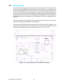
1
User Manual MIC-3392MIL 6U CompactPCI® Intel® Core™ 2 Duo Processor Based Board with Dual PCIe GbE/DDR2/SATA Copyright The documentation and the software included with this product are copyrighted 2010 by Advantech Co., Ltd. All rights are reserved. Advantech Co., Ltd. reserves the right to make improvements in the products described in this manual at any time without notice. No part of this manual may be reproduced, copied, translated or transmitted in any form or by any means without the prior written permission of Advantech Co., Ltd. Information provided in this manual is intended to be accurate and reliable. However, Advantech Co., Ltd. assumes no responsibility for its use, nor for any infringements of the rights of third parties, which may result from its use. Acknowledgements All other product names or trademarks are properties of their respective owners. Product Warranty (2 years) Advantech warrants to you, the original purchaser, that each of its products will be free from defects in materials and workmanship for two years from the date of purchase. This warranty does not apply to any products which have been repaired or altered by persons other than repair personnel authorized by Advantech, or which have been subject to misuse, abuse, accident or improper installation. Advantech assumes no liability under the terms of this warranty as a consequence of such events. Because of Advantech’s high quality-control standards and rigorous testing, most of our customers never need to use our repair service. If an Advantech product is defective, it will be repaired or replaced at no charge during the warranty period. For outof-warranty repairs, you will be billed according to the cost of replacement materials, service time and freight. Please consult your dealer for more details. If you think you have a defective product, follow these steps: 1. Collect all the information about the problem encountered. (For example, CPU speed, Advantech products used, other hardware and software used, etc.) Note anything abnormal and list any onscreen messages you get when the problem occurs. 2. Call your dealer and describe the problem. Please have your manual, product, and any helpful information readily available. 3. If your product is diagnosed as defective, obtain an RMA (return merchandise authorization) number from your dealer. This allows us to process your return more quickly. 4. Carefully pack the defective product, a fully-completed Repair and Replacement Order Card and a photocopy proof of purchase date (such as your sales receipt) in a shippable container. A product returned without proof of the purchase date is not eligible for warranty service. 5. Write the RMA number visibly on the outside of the package and ship it prepaid to your dealer. MIC-3392MIL User Manual Part No. 2002339231 Edition 2 Printed in Taiwan March 2010 ii Declaration of Conformity CE This product has passed the CE test for environmental specifications when shielded cables are used for external wiring. We recommend the use of shielded cables. FCC Class A Note: This equipment has been tested and found to comply with the limits for a Class A digital device, pursuant to part 15 of the FCC Rules. These limits are designed to provide reasonable protection against harmful interference when the equipment is operated in a commercial environment. This equipment generates, uses, and can radiate radio frequency energy and, if not installed and used in accordance with the instruction manual, may cause harmful interference to radio communications. Operation of this equipment in a residential area is likely to cause harmful interference in which case the user will be required to correct the interference at his own expense. FM This equipment has passed the FM certification. According to the National Fire Protection Association, work sites are classified into different classes, divisions and groups, based on hazard considerations. This equipment is compliant with the specifications for Class I, Division 2, Groups A, B, C, and D indoor hazards. Technical Support and Assistance 1. 2. Visit the Advantech web site at www.advantech.com/support where you can find the latest information about the product. Contact your distributor, sales representative, or Advantech's customer service center for technical support if you need additional assistance. Please have the following information ready before you call: – Product name and serial number – Description of your peripheral attachments – Description of your software (operating system, version, application software, etc.) – A complete description of the problem – The exact wording of any error messages iii MIC-3392MIL User Manual Warnings, Cautions and Notes Warning! Warnings indicate conditions, which if not observed, can cause personal injury! Caution! Cautions are included to help you avoid damaging hardware or losing data. e.g. There is a danger of a new battery exploding if it is incorrectly installed. Do not attempt to recharge, force open, or heat the battery. Replace the battery only with the same or equivalent type recommended by the manufacturer. Discard used batteries according to the manufacturer's instructions. Note! Notes provide optional additional information. Document Feedback To assist us in making improvements to this manual, we would welcome comments and constructive criticism. Please send all such - in writing to: [email protected] Packing List MIC-3392MIL all-in-one single board computer (CPU and MCH heatsinks included) x1 Utility and user manual (PDF file) CD-ROM disc x1 HDD tray (Assembled) x 1 for MIC-3392MILS models Daughter board for SATA HDD (Assembled) x1 for MIC-3392MILS models Solder-side cover (Assembled) x1 for MIC-3392MILS models Warranty certificate document x1 Safety Warnings: CE, FCC class A If any of these items are missing or damaged, contact your distributor or sales representative immediately. MIC-3392MIL User Manual iv Safety Instructions 1. 2. 3. Read these safety instructions carefully. Keep this User Manual for later reference. Disconnect this equipment from any AC outlet before cleaning. Use a damp cloth. Do not use liquid or spray detergents for cleaning. 4. For plug-in equipment, the power outlet socket must be located near the equipment and must be easily accessible. 5. Keep this equipment away from humidity. 6. Put this equipment on a reliable surface during installation. Dropping it or letting it fall may cause damage. 7. The openings on the enclosure are for air convection. Protect the equipment from overheating. DO NOT COVER THE OPENINGS. 8. Make sure the voltage of the power source is correct before connecting the equipment to the power outlet. 9. Position the power cord so that people cannot step on it. Do not place anything over the power cord. 10. All cautions and warnings on the equipment should be noted. 11. If the equipment is not used for a long time, disconnect it from the power source to avoid damage by transient overvoltage. 12. Never pour any liquid into an opening in the device. This may cause fire, or electrical shock, or damage to the equipment. 13. Never open the equipment. For safety reasons, the equipment should be opened only by qualified service personnel. 14. If one of the following situations arises, get the equipment checked by service personnel: 15. The power cord or plug is damaged. 16. Liquid has penetrated into the equipment. 17. The equipment has been exposed to moisture. 18. The equipment does not work well, or you cannot get it to work according to the user's manual. 19. The equipment has been dropped and damaged. 20. The equipment has obvious signs of breakage. 21. DO NOT LEAVE THIS EQUIPMENT IN AN ENVIRONMENT WHERE THE STORAGE TEMPERATURE MAY GO BELOW -20° C (-4° F) OR ABOVE 60° C (140° F). THIS COULD DAMAGE THE EQUIPMENT. THE EQUIPMENT SHOULD BE IN A CONTROLLED ENVIRONMENT. 22. CAUTION: DANGER OF EXPLOSION IF BATTERY IS INCORRECTLY REPLACED. REPLACE ONLY WITH THE SAME OR EQUIVALENT TYPE RECOMMENDED BY THE MANUFACTURER, DISCARD USED BATTERIES ACCORDING TO THE MANUFACTURER'S INSTRUCTIONS. 23. The sound pressure level at the operator's position according to IEC 704-1:1982 is no more than 70 dB (A). DISCLAIMER: This set of instructions is given according to IEC 704-1. Advantech disclaims all responsibility for the accuracy of any statements contained herein. v MIC-3392MIL User Manual Safety Precaution - Static Electricity Follow these simple precautions to protect yourself from harm and the products from damage. To avoid electrical shock, always disconnect the power from your PC chassis before you work on it. Don't touch any components on the CPU card or other cards while the PC is on. Take anti-static precautions before making any configuration changes. The sudden rush of power from electrostatic discharge events when you connect a jumper or install a card may damage sensitive electronic components. Product Configurations Front Panel Conduction System Board USB BMC System Cool Model Number VGA 2.0 Reset Reset Main On-board Features CPU Memory CF Storage SODIMM Socket Channel Socket Conformal Coating MIC-3392MILSP1E 1 2 V V - Intel U7500 2 GB 1 1 1 - MIC-3392MILSP2E 1 2 V V - Intel L2400 2 GB 1 1 1 - MIC-3392MILCP1E - - - - V Intel U7500 2 GB 1 - - V MIC3392MILSXP2E 1 2 V V - Intel L2400 2 GB 1 1 1 - RTM Model Number Rear Panel On-board Header/Socket/Connector USB CPCI Conformal COM Console Inter- Conn. Coating LAN COM DVI-I PS2 USB IDE FDD LPT SATA Interface Interface face RIO-3392MILA1E 4 1 2 1 2 1 1 1 2 1 1 2 J3~J5 - RIO-3392MILA2E 4 1 2 1 2 1 1 1 2 1 1 2 J3~J5 V Note! We do not recommend using the MIC-3392MIL as a system board to support a MIC-3951 peripheral carrier board with Advantech's phased out dual gigabit Ethernet PMC cards such as the MIC-3661 and the MIC-3662. We Appreciate Your Input Please let us know of any aspect of this product, including the manual, which could use improvement or correction. We appreciate your valuable input in helping make our products better. MIC-3392MIL User Manual vi Contents Chapter 1 Hardware Configuration......................1 1.1 Introduction ............................................................................................... 2 Table 1.1: MIC-3392MIL Variants................................................ 2 Specifications ............................................................................................ 3 1.2.1 CompactPCI Bus Interface ........................................................... 3 1.2.2 CPU .............................................................................................. 3 Table 1.2: Intel processor selection for the MIC-3392MIL........... 3 1.2.3 BIOS ............................................................................................. 3 1.2.4 Chipset.......................................................................................... 3 1.2.5 Memory ......................................................................................... 4 Table 1.3: DDR2 SODIMM Tested on the MIC-3392MIL ............ 4 1.2.6 Ethernet ........................................................................................ 4 1.2.7 Storage Interface .......................................................................... 4 1.2.8 Serial Interface.............................................................................. 5 1.2.9 USB Port ....................................................................................... 5 1.2.10 LEDs ............................................................................................. 5 1.2.11 Watchdog Timer............................................................................ 5 1.2.12 Optional Rear I/O Modules ........................................................... 5 1.2.13 Mechanical and Environmental Specifications.............................. 6 1.2.14 Compact Mechanical Design ........................................................ 6 1.2.15 CompactPCI Bridge ...................................................................... 6 1.2.16 I/O Connectivity............................................................................. 7 1.2.17 Hardware Monitor ......................................................................... 7 1.2.18 Super I/O....................................................................................... 7 1.2.19 RTC and Battery ........................................................................... 7 1.2.20 IPMI............................................................................................... 7 1.2.21 Pre-Heat on the Conduction-Cooled Model .................................. 8 Functional Block Diagram ......................................................................... 8 Figure 1.1 MIC-3392MIL functional block diagram ...................... 8 Jumpers and Switches .............................................................................. 9 Table 1.4: MIC-3392MIL jumper descriptions.............................. 9 Table 1.5: MIC-3392MIL switch descriptions............................... 9 1.4.1 Jumper Settings ............................................................................ 9 Table 1.6: JP5 VGA Output Setting............................................. 9 Table 1.7: JP7 Compact Flash Master/Slave Mode Selection .... 9 1.4.2 Clear CMOS (JP6) ...................................................................... 10 Table 1.8: JP6 Clear CMOS ...................................................... 10 1.4.3 Switch Settings ........................................................................... 10 Table 1.9: SW1 PCI Bridge Master/Drone Mode Selection....... 10 Table 1.10: SW2 BMC Reset/Platform Reset (available on the Front Panel only) ...................................................... 10 Table 1.11: SW3 SATA Port 1 Channel Setting .......................... 11 Table 1.12: SW4 BMC Firmware Programming/Console Setting 11 Connector Definitions.............................................................................. 12 Table 1.13: MIC-3392MIL connector descriptions....................... 12 Figure 1.2 MIC-3392MIL jumper and switch locations............... 12 1.5.1 VGA Display Connector (VCN1) ................................................. 13 1.5.2 USB Connectors (CN11/12)........................................................ 13 1.5.3 CMOS Battery (BH1) .................................................................. 13 1.5.4 CompactFlash Socket (CN10) .................................................... 13 1.5.5 SATA Daughter Board Connector (CN4) .................................... 13 1.5.6 Pre-heat Heater Pad Power Connector (CN13).......................... 13 Safety Precautions .................................................................................. 14 Installing CompactFlash in the MIC-3392MILC Model............................ 14 1.2 1.3 1.4 1.5 1.6 1.7 vii MIC-3392MIL User Manual 1.7.1 Chapter 1.8 Wedge Locks Removal............................................................... 14 Figure 1.3 Remove the M2 x .40 screws (x4)............................ 14 Figure 1.4 Remove the wedge locks from the conduction-cooled plate.......................................................................... 15 1.7.2 PCB Guide Base Removal ......................................................... 15 Figure 1.5 Remove the M2 screws for the PCB guide bases.... 15 Figure 1.6 Remove the PCB guide bases from the conductioncooled plate .............................................................. 16 1.7.3 Conduction-Cooled Plate Removal............................................. 16 Figure 1.7 Remove the M2.5 screws from the secondary side of the PCB .................................................................... 16 Figure 1.8 Remove the conduction-cooled plate from the board ................................................................................. 17 1.7.4 CF Card Insertion ....................................................................... 17 Figure 1.9 Insert the CF card in CN10....................................... 17 1.7.5 Reassembling the Conduction-cooled Assembly ....................... 18 Figure 1.10PCB guide base (left) assembly orientation ............. 18 Figure 1.11PCB guide base (right) assembly orientation ........... 18 Figure 1.12Wedge lock hexagon socket head cap screw .......... 19 Figure 1.13M2 x.40 screw locations ........................................... 19 Software Support .................................................................................... 20 2 AMI BIOS Setup................................. 21 2.1 Introduction ............................................................................................. 22 Figure 2.1 Setup program initial screen..................................... 22 Entering Setup ........................................................................................ 23 Figure 2.2 Sample BIOS patch code ......................................... 23 Main Setup.............................................................................................. 24 Figure 2.3 Main setup screen .................................................... 24 2.3.1 System Time/System Date ......................................................... 24 Advanced BIOS Features Setup............................................................. 25 Figure 2.4 Advanced BIOS features setup screen .................... 25 2.4.1 CPU Configuration...................................................................... 25 Figure 2.5 CPU configuration .................................................... 25 2.4.2 IDE Configuration ....................................................................... 26 Figure 2.6 IDE configuration...................................................... 26 2.4.3 Floppy Configuration................................................................... 27 Figure 2.7 Floppy configuration ................................................. 27 2.4.4 Super I/O Configuration .............................................................. 28 Figure 2.8 Super I/O configuration ............................................ 28 2.4.5 Hardware Health Configuration .................................................. 29 Figure 2.9 Hardware health configuration ................................. 29 2.4.6 ACPI Setting ............................................................................... 30 Figure 2.10ACPI setting ............................................................. 30 2.4.7 APM Configuration...................................................................... 31 Figure 2.11APM configuration .................................................... 31 2.4.8 Console Redirection Configuration ............................................. 32 Figure 2.12Console re-direction configuration............................ 32 PCI/PnP Setup........................................................................................ 33 Figure 2.13PCI/PnP setup.......................................................... 33 2.5.1 Clear NVRAM ............................................................................. 33 2.5.2 Plug and Play O/S ...................................................................... 33 2.5.3 PCI Latency Timer ...................................................................... 33 Boot Setup .............................................................................................. 34 Figure 2.14Boot setup ................................................................ 34 2.6.1 Boot Settings Configuration ........................................................ 35 Figure 2.15Boot settings configuration ....................................... 35 Security Setup......................................................................................... 36 2.2 2.3 2.4 2.5 2.6 2.7 MIC-3392MIL User Manual viii 2.8 2.9 Chapter 3 Pre-heating for the MIC-3392MIL.......................................41 3.1 Introduction ............................................................................................. 42 Figure 3.1 Pre-heat thermal sensor (DS1631AU) location ........ 42 Figure 3.2 Pin definitions of CN13 ............................................. 43 Pre-heat Firmware Operation.................................................................. 43 3.2.1 Standard Pre-heat Mode............................................................. 43 3.2.2 Extended Pre-heat Mode ............................................................ 44 3.2.3 BMC Communication Interface to the x86 System ..................... 44 Table 3.1: Internal register map for the pre-heat firmware controller................................................................... 45 3.2.4 Read/Write the Internal Registers............................................... 46 Figure 3.3 Set-up for read/write access to the internal registers46 3.2.5 Illustration of Accessing an Internal Register of BMC................. 47 Figure 3.4 <Enter> “debug32” utility .......................................... 47 3.2 Chapter Figure 2.16Password configuration ............................................ 36 Advanced Chipset Settings ..................................................................... 37 Figure 2.17Advanced chipset setting.......................................... 37 2.8.1 North Bridge Chipset Configuration ............................................ 37 Figure 2.18North bridge chipset configuration............................ 37 Figure 2.19Video function configuration ..................................... 38 2.8.2 South Bridge Chipset Configuration............................................ 39 Figure 2.20South bridge chipset configuration ........................... 39 Exit Options............................................................................................. 40 Figure 2.21Exit options ............................................................... 40 2.9.1 Save Changes and Exit .............................................................. 40 2.9.2 Discard Changes and Exit .......................................................... 40 2.9.3 Load Defaults.............................................................................. 40 4 IPMI for the MIC-3392MILS................51 4.1 4.2 4.3 Introduction ............................................................................................. 52 Definitions ............................................................................................... 52 IPMI Function List ................................................................................... 53 4.3.1 IPMI Device Global Commands.................................................. 53 Table 4.1: Supported IPMI device global commands ................ 53 4.3.2 BMC Device and Messaging Interfaces...................................... 53 Table 4.2: H8S I2C bus connection to NIC SMBus ................... 53 Table 4.3: NIC interrupt ............................................................. 53 Table 4.4: BMC device and messaging commands .................. 54 4.3.3 BMC Watchdog Timer Commands ............................................. 54 Table 4.5: BMC watchdog timer commands.............................. 54 4.3.4 Chassis Device Commands........................................................ 55 Table 4.6: Chassis device commands....................................... 55 4.3.5 Event Commands ....................................................................... 55 Table 4.7: Event commands...................................................... 55 4.3.6 PEF and Alerting Commands ..................................................... 55 Table 4.8: PEF and alerting commands .................................... 55 4.3.7 SEL Device Commands.............................................................. 56 Table 4.9: SEL device commands............................................. 56 4.3.8 SDR Device Commands ............................................................. 56 Table 4.10: SDR device commands ............................................ 56 4.3.9 FRU Data .................................................................................... 56 Table 4.11: FRU device commands ............................................ 56 4.3.10 Sensor and Threshold Configuration .......................................... 57 Table 4.12: Sensors list ............................................................... 57 ix MIC-3392MIL User Manual 4.4 Table 4.13: Threshold values of sensors .................................... 58 Table 4.14: Sensor device commands ........................................ 58 4.3.11 Serial/Modem Device Commands .............................................. 58 Table 4.15: Serial Modem device commands ............................. 58 BMC Reset.............................................................................................. 59 Appendix A Pin Assignments............................... 61 A.1 J1 Connector........................................................................................... 62 Table A.1: J1 CompactPCI I/O .................................................. 62 J2 Connector........................................................................................... 63 Table A.2: J2 CompactPCI I/O .................................................. 63 J3 Connector........................................................................................... 64 Table A.3: J3 CompactPCI I/O (LAN1/LAN2, 2.16) ................... 64 J4 Connector........................................................................................... 65 Table A.4: J4 CompactPCI I/O (Audio, LAN3/LAN4, IDE, SATA, USB, and DVI).......................................................... 65 J5 Connector........................................................................................... 66 Table A.5: J5 CompactPCI I/O (USB, PS2, COM, FDD, DVI, and VGA)......................................................................... 66 Other Connector ..................................................................................... 67 Table A.6: CN4 SATA daughter board connector...................... 67 A.2 A.3 A.4 A.5 A.6 Appendix B Pin Assignments............................... 69 B.1 M/D, PWR, BMC HB, and IDE/Hot-swap LEDs ...................................... 70 Appendix C Programming the Watchdog Timer . 71 C.1 Watchdog Timer Programming Procedure ............................................. 72 Appendix D CPLD .................................................. 73 D.1 D.2 Features.................................................................................................. 74 CPLD I/O Registers ................................................................................ 74 Table D.1: LPC I/O registers address ........................................ 74 D.2.1 Debug Message.......................................................................... 74 Table D.2: Debug_Code [7:0] (LPC I/O address: 80H).............. 74 D.2.2 Watchdog Register ..................................................................... 74 Table D.3: Watchdog [7:0] (LPC I/O address: 443H)................. 74 D.2.3 Watchdog Disable Register ........................................................ 75 Table D.4: Watchdog [7:0] (LPC I/O address: 444H)................. 75 Table D.5: Version [7:0] (LPC I/O address: 445H)..................... 75 D.2.4 Geography Address (GA) ........................................................... 75 Table D.6: GA [7:0] (LPC I/O address: 447H)............................ 75 Appendix E Glossary............................................. 77 MIC-3392MIL User Manual x Chapter 1 1 Hardware Configuration This chapter describes how to configure MIC-3392MIL hardware. 1.1 Introduction The MIC-3392MIL is a high performance, power efficient, CompactPCI PICMG2.16 compliant single-board computer based on the Intel Core2 Duo ULV or Core Duo LV microprocessor. Designed to meet a wide range of environmental requirements from ruggedized applications, the MIC-3392MIL delivers breakthrough energy-efficient performance for CompactPCI platforms. Both Intel Core 2 Duo ULV and Core Duo LV processors provide high MIPS-per-watt performance to help equipment manufacturers optimally balance processing capabilities within power and space constraints. Based on the ULV processor in particular, the SBC offers a low power dissipation design without the need of on-board forced ventilation. Ruggedized requirements are addressed by a conduction-cooled design and extended operating temperature range (-40° C ~ 70° C). Shock and vibration resistances of the board are increased by using wedge locks and a single piece of CNC-milled aluminum alloy plate that conforms to the major IC packages. The MIC-3392MIL maximizes I/O throughput with PCI Express (PCIe) technology. It supports up to 3 GB of 667 MHz DDR2 memory provided by a combination of SODIMM and soldered DRAM (6.4 GB/sec throughput). It supports a fast Serial-ATA interface to an on-board hard drive or CompactFlash socket. In addition, combined with a dedicated RTM (or rear I/O module) called RIO-3392-MIL, it offers a rich variety of I/O interfaces for connections. The MIC-3392MIL is available in standard CPCI or rugged conduction cooled variant with different front I/O options as listed in the table below. Table 1.1: MIC-3392MIL Variants Features ‘S’ model standard CPCI ‘C’ model Conduction Cooled VGA 1 - USB2.0 2 - BMC reset V - System reset V - On-board HDD 1 - CF socket 1 1 SODIMM socket 1 - LEDs 4 - MIC-3392MIL User Manual 2 1.2.1 CompactPCI Bus Interface The MIC-3392MIL is compliant with PICMG 2.0 Rev. 3.0. It supports a 64-bit / 66 MHz or 33 MHz PCI bus for up to 7 CompactPCI slots at 3.3 V or 5 V VIO. The MIC3392MIL is hot-swap compliant (PICMG 2.1) and conforms to the CompactPCI Packet Switching Backplane specification (PICMG 2.16) as well as the CompactPCI System Management Specification (PICMG 2.9). (PICMG 2.9) S modle only. The board can be configured as a system master or a drone board. In drone mode it only draws power from the CompactPCI backplane and is not active on the CompactPCI bus. However, PICMG 2.16 is still fully supported in this mode. 1.2.2 CPU The MIC-3392MIL supports the 65nm-technology Intel Core Duo LV and Intel Core 2 Duo ULV processor family with clock frequencies up to 1.66GHz GHz and a FrontSide Bus (FSB) up to 667 MHz. These processors are validated with the Mobile Intel 945GME Express chipset. This chipset provides greater flexibility for developers of embedded applications by offering improved graphics and increased I/O bandwidth over previous Intel chipsets, as well as remote asset management capabilities, and improved storage speed and reliability. Currently supported processors are listed in the table below. The MIC-3392MILC model (conduction cooled) uses the U7500 processor. However, the MIC-3392MILS model can use either the U7500 or the L2400 processor. Table 1.2: Intel processor selection for the MIC-3392MIL Model Core speed FSB speed L2 cache TDP Package Intel Core Duo L2400 1.66 GHz 667 MHz 2 MB 15 W FCBGA Intel Core2 Duo U7500 1.06 GHz 533 MHz 2 MB 10 W FCBGA 1.2.3 BIOS An 8 Mbit Firmware Hub (FWH) contains a board-specific BIOS (from AMI) designed to meet industrial and embedded system requirements. 1.2.4 Chipset The Mobile Intel 945GME chipset provides excellent flexibility for developers of embedded applications by offering improved graphics and increased I/O bandwidth over previous Intel chipsets, as well as remote asset management capabilities and improved storage speed and reliability. Features include an integrated 32-bit 3D graphics engine based on Intel Graphics Media Accelerator 950 (Intel GMA 950) architecture. The Mobile Intel 945GME chipset consists of the Intel 82945GME Graphics Memory Controller Hub (GMCH) and Intel I/O Controller Hub 7-M (ICH7M). It delivers outstanding system performance through high bandwidth interfaces such as PCI Express, Serial ATA and Hi-Speed USB 2.0. 3 MIC-3392MIL User Manual Hardware Configuration Note! Chapter 1 1.2 Specifications 1.2.5 Memory The MIC-3392MIL has 2 GB of on-board non-ECC DDR2 SDRAM. It also has a SODIMM socket that can accommodate an additional 2 GB of memory. However, with Intel 945GME chipset the OS may report a lower amount of total available memory such as 3 GB. The memory range unavailable to the OS will still be utilized by subsystems such as I/O, PCI-Express, and Integrated Graphics. The following table shows a list of SODIMM modules with Advantech P-trade part numbers that have been tested on the MIC-3392MIL. Table 1.3: DDR2 SODIMM Tested on the MIC-3392MIL Brand Size Speed ECC REG Memory chip Transcend 2GB 667 NO NO Micron 7TE17 D9HNL Transcend 512MB 553 NO NO SEC 719 ZCE6 K4T51083QC DSL 512MB PC2-4200 NO NO Elpida Japan E5116AB-5C-E Apacer 1GB PC2-4300 NO NO Elpida TWN E5108AE-5C-E Note! DDR2 SODIMM is supported on the MIC-3392MILS model. 1.2.6 Ethernet The MIC-3392MIL uses one Intel 82571EB LAN controller to provide 10/100/1000 Base-T Ethernet connectivity (LAN1/ LAN2 or PICMG2.16) and one Intel 82546GB LAN controller to provide 10/100 Base-T Ethernet connectivity (LAN3/LAN4) via the RJ-45 ports on the RTM. Optional settings for the source of the Gigabit Ethernet ports (82571EB) can be selected in the BIOS menu. These are mutually exclusive and can be any one of: LAN1/LAN2 of Rear I/O (on the RTM) PICMG 2.16 Note! PICMG 2.16 is used for RTM LAN1 and LAN2. 1.2.7 Storage Interface The MIC-3392MIL supports two SATA channels and one IDE channel. The SATA1 interface can be routed to an onboard 2.5" SATA hard disk drive or to the RTM via the J4 connector. The onboard SATA port is only available on the MIC-3392MILS model. The SATA2 interface is also connected to the RTM via the J4 connector. The MIC3392MIL also supports one IDE channel. The master is reserved for an on-board Type-I CF storage card. The slave is connected to the RTM via the J4 connector. MIC-3392MIL User Manual 4 Three serial interfaces are routed to the RTM via the J5 connector. The first one, implemented as the system console port by default, is available as a RJ-45 COM port on the RIO. The second one is available as COM2 connector on the RTM. And, the third one named COM3 available on the RTM is designed to serve as a console interface to the BMC. 1.2.9 USB Port 1.2.10 LEDs Available on the MIC-3392MILS model, four LEDs are provided on the front panel as follows: One bi-color LED (blue/yellow) indicates hot sway and HDD activity. The blue color indicates that the board may be safely removed from the system, and the yellow color indicates HDD activity. One LED provides power status. When the LED is green, it means power is provided to the board. One LED indicates “Master” or “Drone” mode. The green color stands for “Master”: mode. When the LED is off, the board is in “Drone” mode. One LED indicated BMC heart beat. When it flashes (yellow), it means the BMC is active. 1.2.11 Watchdog Timer An onboard watchdog timer provides system reset capabilities via software control. The programmable time interval is from 1 to 255 seconds. 1.2.12 Optional Rear I/O Modules The RIO-3392MIL is the optional RTM (also known as rear I/O module) for the MIC3392MIL. It offers a wide variety of I/O features, such as four RJ45 LAN ports, one COM port, two DVI-I ports, two USB2.0 ports, and one P/S2 port. It also comes with on-board features such as IDE, parallel, audio, FDD, USB2.0, SATA, console, and COM interfaces (pin-headers). 5 MIC-3392MIL User Manual Hardware Configuration Six USB 2.0/1.1 compliant ports with fuse protection are provided. Two of them are routed to front panel connectors on the MIC-3392MILS model. The other four are routed to the RTM through the J4 and J5 connectors. Chapter 1 1.2.8 Serial Interface 1.2.13 Mechanical and Environmental Specifications Operating temperature (for the MIC-3392MILS models): 0 ~ 70° C (-32 ~ 158° F) Operating temperature (for the MIC-3392MILC & MIC-3392MILSX models): -40 ~ 70° C (-40 ~ 158° F) Storage Temperature: -50 ~ 80° C (-58 ~ 176° F) Humidity (Non-operating): 10 ~ 95% @ 45° C (non-condensing) Power Consumption: MIC-3392MILS model 2GB memory: +5 V @ 5.76 A; +3.3 V @ 8.48 A; +12 V @ 0.21 A MIC-3392MILC model 2GB memory: +5 V @ 5.76 A; +3.3 V @ 8.48 A; +12 V @ 1.04 A Board size: 233.35 x 160 mm (6U size), 1-slot (4 TE) wide Weight: MIC-3392MILS model: 0.97 kg (2.14 lb) MIC-3392MILC model: 1.05 kg (2.31 lb) Shock (without the on-board hard disk drive): 20 G (operating); 50 G (non-operating) Random vibration: 1.5 Grms (operating), 2.0 Grms (non-operating) 1.2.14 Compact Mechanical Design The MIC-3392MILS model has a specially designed copper heat sink for the processor to enable fanless operation. However, forced air cooling in the chassis is still needed for operational stability and reliability. The MIC-3392MILC model uses a conduction-cooled design that complies with ANSI/VITA30.1-2002 specifications. It uses a pair of wedge locks and a single-piece of CNC-milled aluminum alloy plate that conforms to the major IC packages on the primary side of the PCB. 1.2.15 CompactPCI Bridge The MIC-3392MIL uses a PLX PCI 6540 universal bridge as a gateway to an intelligent subsystem. When configured as a system controller, the bridge acts as a standard transparent PCI-X-to-PCI bridge. As a peripheral controller it allows the local MIC-3392MIL processor to configure and control the onboard local subsystem independently from the CompactPCI bus host processor. The MIC-3392MIL local PCI subsystem is presented to the CompactPCI bus host as a single CompactPCI device. When the MIC-3392MIL is in drone mode, the PLX PCI 6540 is electrically isolated from the CompactPCI bus. The MIC-3392MIL receives power from the backplane, supports rear I/O and supports PICMG 2.16. The PLX PCI 6540 PCI bridge offers the following features: PCI Interface – Full compliance with the PCI Local Bus Specification, Revision 2.3 – Supports 3.3V or 5V tolerance I/O Transparent and non-transparent bridge function 64-bit, 33MHz-133MHz asynchronous operation Support for 8 Bus Masters Usable in CompactPCI system slot or peripheral slot MIC-3392MIL User Manual 6 Chapter 1 10-KB Buffer Architecture for PCI-X-to-PCI-X and PCI-X-to-PCI bridging and speed conversion 1-KB downstream Posted Write buffer 1-KB upstream Poster Writer buffer 4-KB downstream Read Data buffer 4-KB upstream Read Data buffer Please consult the PLX PCI 6540 data book for details. 1.2.16 I/O Connectivity 1.2.17 Hardware Monitor One Hardware Monitor (W83627HG) is available to monitor critical hardware parameters. It is attached to the BMC to monitor the CPU temperature and core voltage information. 1.2.18 Super I/O The MIC-3392MIL Super I/O device provides the following legacy PC devices: Serial ports COM1 and COM2 are connected to the rear I/O module. The parallel port is routed to the rear I/O module. The FDD is routed to the rear I/O module. The PS2 (keyboard/mouse) is routed to the rear I/O module. 1.2.19 RTC and Battery The RTC module keeps the date and time. On the MIC-3392MILS model the RTC circuitry is connected to battery sources (CR2032M1S8-LF, 3V, 210mAH), one located on the board and the other on the RIO-3392MIL RTM. For the MIC-3392MILC model, the RTC circuitry can be connected to the battery source on the RIO-3392MIL only. 1.2.20 IPMI The MIC-3392MILS model uses the Intelligent Platform Management Interface (IPMI) to monitor the health of an entire system. A Renesas H8S/2167 microcontroller provides BMC functionality to interface between system management software and platform hardware. The MIC-3392MILS model implements fully-compliant IPMI 2.0 functionality and conforms to the PICMG 2.9 R1.0 specification. The IPMI firmware is based on proven technology from Avocent. Full IPMI details are covered in Chapter 4. 7 MIC-3392MIL User Manual Hardware Configuration For the MIC-3392MIL, the front panel I/O is provided by one VGA port and two USB ports. Its on-board I/O consists of one IDE channel to a Compact Flash socket and one SATA channel which can be connected to a 2.5" SATA HDD. The MIC-3392MILC model does not have a front panel or the on-board SATA HDD module because its entire PCB is covered up by the conduction-cooled plate. For both models, the rear I/ O connectivity is available via the following CompactPCI connectors: J3: two Gigabit Ethernet links to the backplane for PICMG 2.16 packet switch and two LAN ports on the RTM J4: two 10/100 LAN ports, one DVI-I port, two SATA ports, two USB ports, one IDE channel and one audio channel on the RTM J5: one DVI-I port, one VGA interface (also available on the front panel), two USB interfaces, one PS2 port (for keyboard/mouse), one FDD channel, one parallel channel, and three COM interfaces (available as RJ45 port, on-board console interface, and on-board COM interface) on the RTM The MIC-3392MILC model does not have IPMI functionality. 1.2.21 Pre-Heat on the Conduction-Cooled Model For reliable system boot performance under extreme low temperature conditions (e.g. -40° C), the MIC-3392MILC contains a 10W heater for warming up the PCB components when the board temperature is below -30° C. A special firmware implemented on the BMC is designed to control the heater on and off operations. Full preheat details are discussed in Chapter 3. The MIC-3392MILS does not have the pre-heat functionality. 1.3 Functional Block Diagram Figure 1.1 MIC-3392MIL functional block diagram MIC-3392MIL User Manual 8 Table 1.4 and table 1.5 list the jumper and switch functions. Figure 1.2 illustrates the jumper and switch locations. Read this section carefully before changing the jumper and switch settings on your MIC-3392MIL board. Table 1.4: MIC-3392MIL jumper descriptions Function JP5 VGA Output Setting JP6 Clear CMOS JP7 CompactFlash Master/Slave Mode Selection Table 1.5: MIC-3392MIL switch descriptions Number Function SW1 PCI Bridge Master/Drone Mode Selection SW2 BMC Reset/Platform Reset (available on the Front Panel only) SW3 SATA Port 1 Channel Setting SW4 BMC Firmware Programmable/Console Setting 1.4.1 Jumper Settings Table 1.6: JP5 VGA Output Setting Default Front Panel 1-2 1 2 3 RTM 2-3 1 2 3 Table 1.7: JP7 Compact Flash Master/Slave Mode Selection Default IDE Master Closed 1 2 IDE Slave Open 1 2 9 MIC-3392MIL User Manual Hardware Configuration Number Chapter 1 1.4 Jumpers and Switches 1.4.2 Clear CMOS (JP6) This jumper is used to erase CMOS data and reset the system BIOS information. Follow the procedures below to clear the CMOS. 1. Turn off the system. 2. Close jumper JP6 (1-2) for about 3 seconds. 3. Set jumper JP6 as Normal. 4. Turn on the system. The BIOS is reset to its default setting. Table 1.8: JP6 Clear CMOS Default Normal Open 1 2 Clear CMOS Closed 1 2 1.4.3 Switch Settings Table 1.9: SW1 PCI Bridge Master/Drone Mode Selection Master Default On On Drone Off Off Note! Key: represents the switch. Table 1.10: SW2 BMC Reset/Platform Reset (available on the Front Panel only) SW2 (top) BMC Reset SW2 (bottom) Platform Reset MIC-3392MIL User Manual 10 Chapter 1 Table 1.11: SW3 SATA Port 1 Channel Setting On-Board Default On RTM SW3 selects the routing of SATA port 1 channel to either the onboard HDD socket or the RTM. Table 1.12: SW4 BMC Firmware Programming/Console Setting BMC to Console Default Off On Off On Off Off BMC Firmware Programmable On Off On Off On On COM3 on the RIO-3392MIL RTM is connected to the BMC. The BMC firmware can be re-programmed by setting SW4 to “BMC Firmware Programmable” mode. For BMC OOB (out-of-band) support, the default setting of SW4 needs to be resumed. 11 MIC-3392MIL User Manual Hardware Configuration Off 1.5 Connector Definitions Table 1.13 lists the function of each connector and Figure 1.2 illustrates connector locations. Table 1.13: MIC-3392MIL connector descriptions Number Function VCN1 VGA connector CN12 USB port 1 CN11 USB port 2 BH1 CMOS battery CN10 CompactFlash socket CN4 SATA daughter board connector CN13 Pre-heat 10W heater pad power connector SODIMM1 SODIMM socket J1/J2 Primary CompactPCI bus J3/J4/J5 Rear I/O transition Figure 1.2 MIC-3392MIL jumper and switch locations Note! VCN1, CN4, CN11, CN12, and SODIMM available on the MIC3392MILS model only. MIC-3392MIL User Manual 12 1.5.2 USB Connectors (CN11/12) The MIC-3392MIL provides up to six Universal Serial Bus (USB) 2.0 channels. Two front panel USB ports, CN11 and CN12, are available on the MIC-3392MILS model. Four other USB channels are routed to rear I/O via the J4 and J5 connectors. The MIC-3392MIL USB interface complies with USB specification R2.0 and is fuse protected (5 V @ 1.1 A). The USB interface can be disabled in the system BIOS setup. The USB controller default is set to “Enabled”. 1.5.3 CMOS Battery (BH1) A 3 V lithium battery will be available on the MIC-3392MILS model. The conductioncooled model will not have the CMOS battery. 1.5.4 CompactFlash Socket (CN10) The MIC-3392MIL features an on-board CompactFlash (Type I) mass storage device connector. When populated with a flash disk it appears to the user as an ATA (IDE) disk drive with the same functionality and capabilities as a rotating media IDE hard drive. The MIC-3392MIL BIOS includes an option to allow the board to boot from the flash disk. The CompactFlash socket is connected to the IDE interface and 5 V power. UltraDMA is supported and has been tested on a number of devices from different manufacturers. Please contact your local support office in the unlikely event that you have any interoperability issues. 1.5.5 SATA Daughter Board Connector (CN4) The MIC-3392MIL provides two SATA interfaces: SATA port 1 via CN4 connects to the onboard SATA HDD or via the J4 connector to a rear I/O board when selected by switch SW3, and SATA port 2 is directly routed to J4. 1.5.6 Pre-heat Heater Pad Power Connector (CN13) The CN13 connector is to be used specifically by the heater pad in the MIC3392MILC model. The heater pad, attached to the back side of the conductioncooled plate, is used to warm up the board during boot up when the ambient temperature reaches below -30° C (-22° F). Approximately 10 watts of electrical power is consumed by the heater pad. 13 MIC-3392MIL User Manual Hardware Configuration The MIC-3392MILS incorporates the Intel 945GME Graphic Memory Controller Hub (GMCH). The Intel Graphics Media Accelerator 950 (Intel GMA 950) graphics core is an intelligent and responsive graphics engine built into the chipset. This integration provides incredible visual quality, faster graphics performance and flexible display options without the need for a separate graphics card. The Intel GMA 950 operates at 256-bit core speeds of up to 400 MHz. The GMA 950 graphics core supports a bandwidth of up to 10.6 GB/sec with up to 224 MB of DDR2 667 video memory. The maximum resolution is 2048 x 1536 at 75 Hz. The VCN1 connector of MIC-3392MILS provides DB-15 connector for the VGA monitor. The system monitor display is routed to either the front panel or the rear I/O module depending on the position of jumper JP5. Chapter 1 1.5.1 VGA Display Connector (VCN1) 1.6 Safety Precautions Follow these simple precautions to protect yourself from harm and the products from damage. To avoid electric shock, always disconnect the power from your CompactPCI chassis before you work on it. Don’t touch any components on the CPU board or other boards while the CompactPCI chassis is powered. Disconnect power before making any configuration changes. The sudden rush of power as you connect a jumper or install a board may damage sensitive electronic components. Always ground yourself to remove any static charge before you touch your CPU board. Be particularly careful not to touch the chip connectors. Modern integrated electronic devices, especially CPUs and memory chips, are extremely sensitive to static electric discharges and fields. Keep the board in its antistatic packaging when it is not installed in the chassis, and place it on a static dissipative mat when you are working with it. Wear a grounding wrist strap for continuous protection. 1.7 Installing CompactFlash in the MIC-3392MILC Model The CF socket (CN10) for the MIC-3392MILC model is beneath the conductioncooled plate, therefore installing a CF card on this particular model requires removing the conduction-cooled plate from the PCB first. The following steps illustrate the removal of the plate and the installation of the CF card. 1.7.1 Wedge Locks Removal Each wedge lock is secured to the conduction-cooled plate by two M2 x .40 screws, which can be accessed on the PCB guide base located on the secondary side of the PCB. There are two wedge locks, two PCB guide bases, and four M2 x .40 screws on the MIC-3392MILC. See Figures 1.3 and 1.4 for illustration. Figure 1.3 Remove the M2 x .40 screws (x4) MIC-3392MIL User Manual 14 Chapter 1 1.7.2 PCB Guide Base Removal Each of the two PCB guide bases is fastened to the conduction-cooled plate by three M2 screws, which can be accessed from the primary side of the board. Figure 1.5 Remove the M2 screws for the PCB guide bases 15 MIC-3392MIL User Manual Hardware Configuration Figure 1.4 Remove the wedge locks from the conduction-cooled plate Figure 1.6 Remove the PCB guide bases from the conduction-cooled plate 1.7.3 Conduction-Cooled Plate Removal To gain access to the CF socket (CN10), the conduction-cooled plate must be removed. There are sixteen M2.5 screws to be removed before the plate can be retrieved. Caution must be taken when taking the plate away from the PCB because the heater pad’s power input wire is still connected to connector CN13. Figure 1.7 Remove the M2.5 screws from the secondary side of the PCB MIC-3392MIL User Manual 16 Chapter 1 1.7.4 CF Card Insertion After the conduction-cooled plate is removed, a CF card (Type-1) can be installed in CN10 as shown below. Figure 1.9 Insert the CF card in CN10 17 MIC-3392MIL User Manual Hardware Configuration Figure 1.8 Remove the conduction-cooled plate from the board 1.7.5 Reassembling the Conduction-cooled Assembly After the CF card is installed, the conduction-cooled plate should be re-installed on the PCB. First reattach the heater pad’s power input connector to CN13, then reattach the two PCB guide bases. Please note that the PCB guide base must be installed in a specific direction; the “L” step must face the PCB as shown in the following figures. The conduction-cooled plate requires sixteen M2.5 screws, and each PCB guide base needs three M2 screws. The recommended torque values for the M2.5 and M2 screws are 3.0±0.5 kgf·cm and 2.2±0.5 kgf·cm, respectively. Figure 1.10 PCB guide base (left) assembly orientation Figure 1.11 PCB guide base (right) assembly orientation MIC-3392MIL User Manual 18 Figure 1.13 M2 x.40 screw locations Note! To achieve the proper clamping and retention forces on the cold-plates of a conduction-cooled chassis (VITA30.1 compliant), the recommended torque for the hexagon socket head cap screw on the wedge lock is 8.2 kgf·cm. 19 MIC-3392MIL User Manual Hardware Configuration Figure 1.12 Wedge lock hexagon socket head cap screw Chapter 1 The wedge locks should be reinstalled with a specific orientation to the board so that the conduction-cooled plate and the PCB guide bases interlock with the PCB. The 2.5 mm hexagon socket head cap screw on the wedge lock must face towards the front end of the board. Each wedge lock uses two M2 x .40 screws. The recommended torque value for the M2 screws is 2.2±0.5 kgf·cm. 1.8 Software Support Windows XP, Windows 2003, Windows Vista and Fedora Core 5 have been fully tested on the MIC-3392MIL. Please contact your local sales representative for details on support for other operating systems. MIC-3392MIL User Manual 20 Chapter 2 2 AMI BIOS Setup This chapter describes how to configure the AMI BIOS. 2.1 Introduction The AMI BIOS has been customized and integrated into many industrial and embedded motherboards for over a decade. This section describes the BIOS which has been specifically adapted to the MIC-3392MIL. With the AMI BIOS Setup program, you can modify BIOS settings and control the special features of the MIC-3392MIL. The Setup program uses a number of menus for making changes and turning the special features on or off. This chapter describes the basic navigation of the MIC3392MIL setup screens. Figure 2.1 Setup program initial screen The BIOS ROM has a built-in Setup program that allows users to modify the basic system configuration. These settings are stored in battery-backed up CMOS so they are retained when the power is turned off. MIC-3392MIL User Manual 22 Turn on the computer, and there should be a “patch code” that shows the BIOS details including date, version number, etc. If there is no number assigned to the patch code, please contact an Advantech application engineer to obtain an up-todate patch code file. This will ensure that the CPU’s system status is valid. After ensuring that you have a number assigned to the patch code, press <DEL> and you will immediately be allowed to enter Setup. Chapter 2 2.2 Entering Setup AMI BIOS Setup Figure 2.2 Sample BIOS patch code 23 MIC-3392MIL User Manual 2.3 Main Setup When you first enter the BIOS Setup Utility, you will enter the Main setup screen. You can always return to the Main setup screen by selecting the Main tab. Two main setup options are described in this section. The main BIOS setup screen is shown below. Figure 2.3 Main setup screen The main BIOS setup menu screen has two main frames. The left frame displays all the options that can be configured. “Grayed-out” options cannot be configured whilst options in blue can. The right frame displays the key legend. Above the key legend is an area reserved for a text message. When an option is selected in the left frame, it is highlighted in white. Often a text message will accompany it. 2.3.1 System Time/System Date Use this option to change the system time and date. Highlight System Time or System Date using the <Arrow> keys. Enter new values through the keyboard. Press the <Tab> key or the <Arrow> keys to move between fields. The date must be entered in MM/DD/YY format. The time is entered in HH:MM:SS format. MIC-3392MIL User Manual 24 Select the Advanced tab from the MIC-3392MIL setup screen to enter the Advanced BIOS Setup screen. You can select any of the items in the left frame of the screen, such as CPU Configuration, to go to the sub menu for that item. You can display an Advanced BIOS Setup option by highlighting it using the <Arrow> keys. All Advanced BIOS Setup options are described in this section. The Advanced BIOS Setup screen is shown below. The sub menus are described on the following pages. Chapter 2 2.4 Advanced BIOS Features Setup AMI BIOS Setup Figure 2.4 Advanced BIOS features setup screen 2.4.1 CPU Configuration Figure 2.5 CPU configuration 25 MIC-3392MIL User Manual 2.4.1.1 Max CPUID Value Limit It is recommended that you leave this value at the default setting of Disabled. 2.4.1.2 Core Multi-Processing This item specifies the CPU to perform multi-processing. The default setting for this item is set to “Enabled”. 2.4.1.3 CPU TM Function This item specifies the Thermal Monitor Feature. If set to “Enabled”, the BIOS enables the CPU’s built-in automatic thermal throttling when the die temperature approaches the processor’s temperature limit. If set to “Disabled”, the MIC-3392MIL will shut off automatically if the CPU overheats. The default setting is “Enabled”. 2.4.2 IDE Configuration Figure 2.6 IDE configuration 2.4.2.1 ATA/IDE Configuration Three options are available: Disabled, Compatible, or Enhanced. “Disabled” means that all IDE resources are disabled. “Compatible” enables up to two IDE channels for OSs requiring legacy IDE operation (default setting). And, “Enhanced” enables all SATA and PATA resources. 2.4.2.2 Legacy IDE Channels Four options are available: “SATA Only”, “Reserved”, “SATA Pri, PATA Sec”, or “PATA Only”. 2.4.2.3 Primary IDE Master and Slave While entering setup, BIOS auto detects the presence of IDE devices. This displays the status of auto detection of the two possible IDE devices. MIC-3392MIL User Manual 26 Figure 2.7 Floppy configuration Floppy A: Select the type of floppy drive connected to the system. 27 MIC-3392MIL User Manual AMI BIOS Setup Chapter 2 2.4.3 Floppy Configuration 2.4.4 Super I/O Configuration Figure 2.8 Super I/O configuration Onboard Floppy Controller: Used to enable or disable the on-board floppy controller (in the Super I/O). Floppy Drive Swap: Set this option to “Enabled” to specify that floppy drives A: and B: are swapped. The setting can be “Enabled” or “Disabled”. Serial Port1 Address: Used to select Serial Port1 base addresses. Serial Port2 Address: Used to select Serial Port2 base addresses. Serial Port2 Mode: Used to select mode for Serial Port2. Parallel Port Address: Used to select Parallel Port base addresses. Parallel Port Mode: Used to select Parallel Port mode. Parallel Port IRQ: Used to select Parallel Port IRQ. MIC-3392MIL User Manual 28 Figure 2.9 Hardware health configuration H/W Health Function: Used to enable or disable hardware health event monitoring such as system (ambient) temperature, CPU temperature, CPU Vcore, system 3.3V, 5V, 12V and -12V input voltages, and the on-board 3V CMOS battery voltage level. Show VBAT Voltage: Used to enable or disable the reading of the on-board 3V battery voltage level. Note! Set Show VBAT Voltage to “Disabled” when no CMOS battery is installed on the board. 29 MIC-3392MIL User Manual AMI BIOS Setup Chapter 2 2.4.5 Hardware Health Configuration 2.4.6 ACPI Setting Figure 2.10 ACPI setting Two types of power management technologies are supported by the MIC-3392MIL: ACPI and APM. ACPI is the newer of the two technologies and puts power management in the hands of the operating system. APM is controlled by the BIOS. Only one power management interface (ACPI or APM) can be in control of the system at a time. The options for “ACPI Aware O/S” are “Yes” or “No,” which either enable or disable ACPI support for the operating system. The default setting is “Yes”. MIC-3392MIL User Manual 30 Chapter 2 2.4.7 APM Configuration Note! When both ACPI and APM modes are enabled at the same time on the BIOS setup, the former power management control will take precedence if the OS supports ACPI mode. In the event that the OS is unaware of ACPI, APM will take control. Hard Disk Power Down Mode: Used to power down the hard disk drive in “Suspend” mode. The default setting for this feature is “Disabled”. Throttle Slow Clock Ratio: Used to select the duty cycle of the CPU in throttle mode. The default setting for this feature is “50%”. Keyboard & PS/2 Mouse: Allows the system to monitor KBC Ports 60/6. 31 MIC-3392MIL User Manual AMI BIOS Setup Figure 2.11 APM configuration APM allows the BIOS to control the system’s power management without the knowledge of the operating system. The default setting for “Power Management/APM” is “Enabled”. 2.4.8 Console Redirection Configuration Figure 2.12 Console re-direction configuration 2.4.8.1 Remote Access You can disable or enable the BIOS remote access feature here. The default setting is “Enabled”. 2.4.8.2 Serial Port Number Select the serial port you want to use for console redirection. You can set the value for this option to either SIO COM1 or COM2. The default setting is SIO COM1. 2.4.8.3 Serial Port Mode Select the baud rate you want the serial port to use for console redirection. The default setting is 115200 8, n, 1. 2.4.8.4 Flow Control Select the flow control setting for the console re-direction - “None”, “Hardware”, and “Software”. The default setting is “None”. MIC-3392MIL User Manual 32 Select the PCI/PnP tab from the MIC-3392MIL setup screen to enter the Plug and Play BIOS Setup screen. You can display a Plug and Play BIOS Setup option by highlighting it using the <Arrow> keys. All Plug and Play BIOS Setup options are described in this section. The Plug and Play BIOS Setup screen is shown below. Chapter 2 2.5 PCI/PnP Setup AMI BIOS Setup Figure 2.13 PCI/PnP setup 2.5.1 Clear NVRAM Set this value to force the BIOS to clear the Non-Volatile Random Access Memory (NVRAM). The default setting is “No”. 2.5.2 Plug and Play O/S Set this value to allow the system to modify the settings for Plug and Play operating system support. The default setting is “No”. 2.5.3 PCI Latency Timer This option sets the latency of all PCI devices on the PCI bus. The default setting is 64. 33 MIC-3392MIL User Manual 2.6 Boot Setup Figure 2.14 Boot setup Note! “Hard Disk Drives” will only appear on the setup screen when at least one hard disk drive is connected to the MIC-3392MIL. MIC-3392MIL User Manual 34 Figure 2.15 Boot settings configuration Quick Boot: Allows the BIOS to skip certain tests while booting. This will decrease the time needed to boot the system. The default setting is on “Enabled”. Boot From LAN Support: Used to set the system bootable from LAN. The default setting is on “Disabled”. Quiet Boot: Used to display OEM logo when the setting is “Enabled”. The default setting, “Disabled”, displays normal POST messages. Bootup Num-Lock: On the default setting, “Enabled”, the Num-Lock key is enabled during system power on. PS/2 Mouse Support: Select support for PS/2 mouse - “Disabled”, “Enabled”, and “Auto”. The default setting is on “Auto”. Wait For ’F1’ If Error: Wait for the F1 key to be pressed if an error occurs. Hit ‘DEL’ Message Display: Displays “Press DEL to run Setup” in POST. 35 MIC-3392MIL User Manual AMI BIOS Setup Chapter 2 2.6.1 Boot Settings Configuration 2.7 Security Setup Figure 2.16 Password configuration Select Security Setup from the MIC-3392MIL Setup main BIOS setup menu. All Security Setup options, such as password protection and virus protection, are described in this section. To access the sub menu for the following items, select the item and press <Enter>: Change Supervisor Password Change User Password Clear User Password MIC-3392MIL User Manual 36 Chapter 2 2.8 Advanced Chipset Settings 2.8.1 North Bridge Chipset Configuration Figure 2.18 North bridge chipset configuration DRAM Frequency: Available settings are “Auto” (default), “400MHz”, “533MHz”, and “667MHz”. Configure DRAM timing by SPD: Available settings are “Enable” (default) and “Disabled”. Internal Graphics Mode Select: Available settings are “Enabled, 8 MB” (default), “Enabled, 1 MB”, and “Disabled”. 37 MIC-3392MIL User Manual AMI BIOS Setup Figure 2.17 Advanced chipset setting 2.8.1.1 Video Function Configuration Figure 2.19 Video function configuration DVMT Mode Select: Available settings are “DVMT Mode” (default), “Fixed Mode”, and “Combo Mode”. – DVMT Mode: the 945GME will dynamically allocate system memory as graphics memory when graphics-intensive applications are running. However, when the need for graphics memory drops, the allocated graphics memory can be released to the operating system for other uses. – Fixed Mode: Unlike the DVMT mode, the graphics driver will reserve a fixed portion of the system memory as graphics memory. – Combo Mode: the graphics driver will allocate a minimum fixed amount of memory as dedicated graphics memory, as well as allow more system memory to be dynamically allocated between the graphics processor and the operating system. DVMT/Fixed Memory: Available only to “DVMT Mode and Fixed Mode”. Settings are “128 MB” (default), “64 MB”, and “Maximum DVMT”. Boot Display Device: Available settings are “Auto” (default), “CRT”, “DVI1”, and “CRT and DVI1”. MIC-3392MIL User Manual 38 Figure 2.20 South bridge chipset configuration USB 2.0 Controller: Settings are “Enabled” (default) and “Disabled”. 39 MIC-3392MIL User Manual AMI BIOS Setup Chapter 2 2.8.2 South Bridge Chipset Configuration 2.9 Exit Options Figure 2.21 Exit options 2.9.1 Save Changes and Exit When you have completed the system configuration changes, follow these steps: 1. Select Exit Saving Changes from the Exit menu and press <Enter>. The following messages appear on the screen: Save Configuration Changes and Exit Now? [Ok] [Cancel] 2. Select “Ok” to save changes and exit. 2.9.2 Discard Changes and Exit Follow these steps to quit Setup without making any permanent changes to the system configuration. 1. Select Exit Discarding Changes from the Exit menu and press <Enter>. The following messages appear on the screen: Discard Changes and Exit Setup Now? [Ok] [Cancel] 2. Select “Ok” to discard changes and exit. The following message appears on the screen: Discard Changes 3. Select “Discard Changes” from the Exit menu and press <Enter>. 2.9.3 Load Defaults This loads the safe defaults values for the MIC-3392MIL which allows optimum general functionality and system performance, but may not work best for all computer applications. Select “Load Defaults” from the Exit menu and press <Enter>. MIC-3392MIL User Manual 40 Chapter 3 3 Pre-heating for the MIC-3392MILC This chapter describes how the pre-heat feature works for the MIC-3392MILC. 3.1 Introduction The pre-heat feature provides an automatic control mechanism for the reliable cold bootup of the MIC-3392MILC. Equipped with a heat pad on the conduction-cooled plate and special BMC firmware for its control, if the ambient board temperature is too low for stable power-on, the preheating circuit powers up the heat pad and keeps the board in reset until the board temperature reaches a safe operating temperature. An alternative pre-heat mode (user configurable) will additionally use the chipset and CPU to generate power dissipation by de-asserting the reset for configurable time intervals. The cold boot control mechanism is only activated upon board startup and does not perform monitoring during standard board operation. A thermal sensor (DS1631AU) located between the CPU and the PCI-bridge on the primary side of the board is used to monitor the ambient board temperature during boot-up. The operating range of this thermal sensor is -55° C to 125° C. Figure 3.1 Pre-heat thermal sensor (DS1631AU) location MIC-3392MIL User Manual 42 Note! More +12 V power to the pre-heat pad can be made available via pins 1 through 3 on CN13, with customized J3 ~ J5 pin definitions and CompactPCI backplane. 3.2 Pre-heat Firmware Operation The pre-heat code in the firmware will be executed when the board temperature (as measured by DS1631AU) is below a predefined threshold (TEMP_PREHEAT) and the board is powered on. By default, TEMP_PREHEAT is set at -30° C. The pre-heat code can be configured to operate in one of two different modes by setting the PREHEAT_MODE register to the appropriate value. The modes are Standard Pre-heat, and Extended Pre-heat. 3.2.1 Standard Pre-heat Mode As a default pre-heat mode, the firmware code will keep the system reset asserted when the payload power is enabled. It will activate the pre-heat circuit by turning on the appropriate GPIO pin and will: Constantly monitor if the payload is switched off again -> turn off preheat circuit and return to the firmware code’s application main loop. Constantly monitor board temperature and de-assert the system reset once the board temperature rises above TEMP_PREHEAT. It shall keep the preheat circuit enabled and keep monitoring the board temperature. The preheat circuit will only be switched off after the temperature rises after a predefined TEMP_PREHEAT + TEMP_HIST. Note! TEMP_HIST = Positive temperature hysteresis for preheat circuit deactivation. The default value of the TEMP_HIST is 0° C. 43 MIC-3392MIL User Manual Pre-heating for the MIC-3392MILC Figure 3.2 Pin definitions of CN13 Chapter 3 A heater pad (70 mm x 80 mm) attached to the interior side of the conduction-cooled plate is capable of providing approximately 10 watts of thermal power when required. Its power input wire is connected to CN13. It gets a +12 V (with 0.8 A) input from two J5 connector pins. The following figure illustrates the pin definitions of CN13. 3.2.2 Extended Pre-heat Mode The extended preheat mode will have the same implementation as the standard preheat mode but will add one extra feature: During the warm up phase, the BMC will repeatedly de-assert the system reset for PREHEAT_TON and then assert it for PREHEAT_TOFF to cause extra power dissipation by CPU and chipset. Note! PREHEAT_TON = Time duration [second] of system reset de-assertion in extended pre-heat mode. PREHEAT_TOFF = Time duration [second] of system reset assertion in extended pre-heat mode. 3.2.3 BMC Communication Interface to the x86 System The BMC will provide a LPC based communication interface to the x86 system, providing access to internal registers. Some of the register settings will be user configurable defaults which will be stored in the SEEPROM. The LPC interface will be interrupt based, and the read/write accesses to the internal registers will be carried out within the interrupt handler. If a write access has taken place and the SEEPROM will have to be updated, the interrupt handler will set a global flag to indicate to the application main loop that updated settings will need to be written to the SEEPROM. The LPC based register interface will consist of an index and data register. The following table shows the internal register map pertaining to the pre-heat function. MIC-3392MIL User Manual 44 INDEX [Hex] Description Direction Default Value [Hex] 0x00 DEVID_MSB Device ID register MSB read only (FW fixed) 0x33 0x01 DEVID_LSB Device ID register LSB 0x02 FW_REV_MSB FW version register MSB read only (FW fixed) xx 0x03 FW_REV_LSB FW version register LSB read only (FW fixed) xx 0x08 REG_SCRATCH Scratch register read write (static init) 0x00 0x10 TEMP_DS1631 DS1613 temp value read only (dynamic reading) xx 0x20 TEMP_PREHEAT Temperature limit for preheat circuit activation read write (stored in EEPROM) 0xE2 = -30° C signed 8 bit value (-128 .. 127) 0x21 TEMP_HIST Positive hysteresis for preheat read write (stored in EEPROM) circuit deactivation 0x00 = 0° C 0x30 PREHEAT_MODE 0 = standard preheat mode 1 = extended preheat mode read write (stored in EEPROM) 0x01 0x31 PREHEAT_TON Time duration of system reset read write (stored in EEPROM) de-assertion in extended mode (seconds) 0x05 0x32 PREHEAT_TOFF Time duration of system reset assertion read write (stored in EEPROM) in extended mode (seconds) 0x01 read only (FW fixed) 0x92 MIC-3392MIL User Manual Pre-heating for the MIC-3392MILC 45 Chapter 3 Table 3.1: Internal register map for the pre-heat firmware controller 3.2.4 Read/Write the Internal Registers The user will need the following items to build the setup as shown in Figure 3.3 in order to gain access to the internal registers for the pre-heat function. MIC-3392MILC RIO-3392MIL CompactPCI chassis (or backplane with at least a system slot) that can accommodate both the MIC-3392MILC and RIO-3392MIL CompactPCI power supply USB or PS/2 Keyboard USB floppy disk drive Floppy disk containing MS-DOS and a DOS utility called “debug32.exe” A LCD monitor A DVI-I cable for display connection between the LCD monitor and the DVI-I port on the RIO-3392MIL Figure 3.3 Set-up for read/write access to the internal registers MIC-3392MIL User Manual 46 Power up the equipment set-up as shown in Figure 3.3 and boot to DOS. Type in “debug32” on the DOS prompt and press <Enter> key (see Figure 3.4). 3.2.5.1 Read DS1631AU’s Temperature Reading (TEMP_DS1631) The index register for the DS1631 thermal sensor’s temperature reading is 0x10 (see Table 3.1). On the “-” prompt, type in “o 294 10” and press <Enter> On the “-” prompt, type in “i 290” and press <Enter> The response would be a hex number that represents the current reading of the DS1631AU thermal sensor. For example, “19” represents “25° C”. Note! “o” represents “writing to” or “locating” a register. “294 xx” represents “index register xx”. “o 294 xx” represents “locating the index register xx”. “i” represents “reading from” a register. “290” represents “data register”. “i 290” represents reading the value in the data register of the located index register xx. 47 MIC-3392MIL User Manual Pre-heating for the MIC-3392MILC Figure 3.4 <Enter> “debug32” utility Chapter 3 3.2.5 Illustration of Accessing an Internal Register of BMC 3.2.5.2 Modify Temperature Limit for Pre-heat Circuit Activation (TEMP_PREHEAT) The index register for TEMP_PREHEAT is 0x20 (see Table 3.1). The default value for the pre-heat circuit activation is “E2” (-30° C), which can be modified as follows. For example, change the temperature limit from -30° C (E2) to -20° C (EC). On the “-” prompt, type in “o 294 20” and press <Enter> On the “-” prompt, type in “o 290 ec” and press <Enter> On the “-” prompt, type in “o 294 20” and press <Enter> On the “-” prompt, type in “i 290” and press <Enter> And, the response shown on the display is “ec”, representing -20° C. At this point, the new setting will be stored automatically in the SEEPROM. Note! It is recommended that the data value for TEMP_PREHEAT does not exceed -5° C (FB). 3.2.5.3 Change Pre-heat Mode (PREHEAT_MODE) The index register for PREHEAT_MODE is 0x30 (see Table 3.1). Its default value is 0x01 (i.e. extended pre-heat mode). To change it to the standard mode (0x00), refer to the following steps. On the “-” prompt, type in “o 294 30” and press <Enter> On the “-” prompt, type in “o 290 00” and press <Enter> On the “-” prompt, type in “o 294 30” and press <Enter> On the “-” prompt, type in “i 290” and press <Enter> And, the response shown on the display is “00”, representing standard pre-heat mode. At this point, the new setting will be stored automatically in the SEEPROM. 3.2.5.4 Exit Debug32 Every time a new value is keyed in to a configurable data register, it will be stored automatically in the SEEPROM. The value will not change until it is re-configured by the user again. To exit the pre-heat configuration mode, type in “quit” on the “”prompt. MIC-3392MIL User Manual 48 Equivalent Hex Value Degrees Celsius Equivalent Hex Value 0 00 1 01 -1 FF 2 02 -2 FE 3 03 -3 FD 4 04 -4 FC 5 05 -5 FB 6 06 -6 FA 7 07 -7 F9 8 08 -8 F8 9 09 -9 F7 10 0A -10 F6 11 0B -11 F5 12 0C -12 F4 13 0D -13 F3 14 0E -14 F2 15 0F -15 F1 16 10 -16 F0 17 11 -17 EF 18 12 -18 EE 19 13 -19 ED 20 14 -20 EC 21 15 -21 EB 22 16 -22 EA 23 17 -23 E9 24 18 -24 E8 25 19 -25 E7 26 1A -26 E6 27 1B -27 E5 28 1C -28 E4 29 1D -29 E3 30 1E -30 E2 31 1F -31 E1 32 20 -32 E0 33 21 -33 DF 34 22 -34 DE 35 23 -35 DD 36 24 -36 DC 37 25 -37 DB 38 26 -38 DA 39 27 -39 D9 40 28 -40 D8 49 MIC-3392MIL User Manual Pre-heating for the MIC-3392MILC Degrees Celsius Chapter 3 3.2.5.5 Temperature Conversion Table MIC-3392MIL User Manual 50 Chapter 4 4 IPMI for the MIC3392MILS This chapter describes IPMI configuration for the MIC-3392MILS. 4.1 Introduction The MIC-3392MILS fully supports the IPMI 2.0 interface and the PICMG 2.9 R1.0 specification. The Renesas H8S/2167 has been implemented as the IPMI controller / Baseboard Management Controller (BMC) to run firmware and collect information. The MIC-3392MILS IPMI firmware is sourced from Avocent, a provider of proven and tested IPMI implementations in a wide range of mission-critical applications. The BMC’s key features and functions are listed below. Compliant with IPMI specification, revision 2.0 Compliant with PICMG 2.9 specification Environment monitoring (temperature and voltage) Power/Reset control via IPMI chassis command Complete SEL, SDR and FRU functionality FRU data capacity: 2 KB Provides 4 messaging interfaces One serial port One LPC interface One IPMB channel One LAN channel messaging via sideband NIC for out-of-band management Four I2C buses (including IPMB and SMBus) and two optional others Firmware Hub flashing and updating over serial port One hardware monitor One interrupt input Sensors threshold configuration Complete IPMI watchdog functionality (reset, power down, power cycle) Platform even filtering (PEF) and alert policies External Event Generation 4.2 Definitions BMC - (Baseboard Management Controller): This is the common abbreviation for an IPMI Baseboard Management Controller. IPMB - (Intelligent Platform Management Bus): A protocol defined for passing IPMI messages over a public I2C bus. IPMI - (Intelligent Platform Management Interface): A standardized system management interface. Please refer to the IPMI Specification for more details. IPMIv2.0: Specifically version 2.0 of IPMI MIC-3392MIL User Manual 52 The following standard IPMI commands are supported. Note! 4.3.1 IPMI Device Global Commands Table 4.1: Supported IPMI device global commands IPMI Device Global Commands NetFn Cmd Mandatory / Optional Get Device Id App 0x01 M Cold Reset App 0x02 O Get Self Test Results App 0x04 M Manufacturing Test On App 0x05 O Set ACPI Power State App 0x06 O Get ACPI Power State App 0x07 O Get Device GUID App 0x08 O 4.3.2 BMC Device and Messaging Interfaces The BMC messaging interfaces comply with the Intelligent Platform Management Interface Specification, Version 2.0. The MIC-3392MILS provides 3 messaging interface channels. LPC/KCS channel: Connects the H8S/2167 to the system LPC bus. Firmware sets 1 host interface over LPC: KCS for SMS. IPMB channel: Connects IPMB devices or connects to the H8S/2167’s I2C_0 interface. Serial port: The H8S/2167 supports one serial port for out-of-band management (OOB) as well as one other serial port for firmware flash update. Table 4.2: H8S I2C bus connection to NIC SMBus H8S/2167 Pin Name I2C_1 SCL1 I2C address 0xC6 SDA1 Pin Number System Connection 48 NIC SMBus clock 47 NIC SMBus data Table 4.3: NIC interrupt H8S/2167 Pin Name Pin Number Usage IRQ1# 130 SMALERT# for NIC SMBus 53 MIC-3392MIL User Manual IPMI for the MIC-3392MILS The Network function (NetFn) field identifies the functional class of the message. The Network Function clusters IPMI commands into different sets. Please refer to the IPMI specification of network function codes for more information. These command codes are compliant with the IPMI specification. Mandatory and Optional commands are defined in the IPMI specification. For more details, please refer to the IPMI specification. Chapter 4 4.3 IPMI Function List Table 4.4: BMC device and messaging commands BMC Device and Messaging Commands NetFn Cmd Mandatory / Optional Set BMC Global Enables App 0x2e M Get BMC Global Enables App 0x2f M Clear Message Flags App 0x30 M Get Message Flags App 0x31 M Enable Message Channel Receive App 0x32 O Get Message App 0x33 M Send Message App 0x34 M Read Event Message Buffer App 0x35 O Get System GUID App 0x37 O Get Channel Authentication Capabilities App 0x38 O Get Session Challenge App 0x39 O Activate Session App 0x3a O Set Session Privilege Level App 0x3b O Close Session App 0x3c O Get Session Information App 0x3d O Get AuthCode App 0x3f O Set Channel Access App 0x40 O Get Channel Access App 0x41 O Get Channel Info App 0x42 O Set User Access App 0x43 O Get User Access App 0x44 O Set User Name App 0x45 O Get User Name App 0x46 O Set User Password App 0x47 O Master Write-Read App 0x52 M 4.3.3 BMC Watchdog Timer Commands Table 4.5: BMC watchdog timer commands BMC Watchdog Timer Commands NetFn Cmd Mandatory / Optional Reset Watchdog Timer App 0x22 M Set Watchdog Timer App 0x24 M Get Watchdog Timer App 0x24 M MIC-3392MIL User Manual 54 Table 4.6: Chassis device commands NetFn Cmd Mandatory/ Optional Get Chassis Capabilities Chassis 0x00 M Get Chassis Status Chassis 0x01 M Chassis Control Chassis 0x02 M Chassis Identify Chassis 0x04 O Set Chassis Capabilities Chassis 0x05 O Get System Restart Cause Chassis 0x07 O Set System Boot Options Chassis 0x08 O Get System Boot Options Chassis 0x09 O Set Front Panel Button Enables Chassis 0x0a O Set Power Cycle Interval Chassis 0x0b O NetFn Cmd Mandatory/ Optional 4.3.5 Event Commands Table 4.7: Event commands Event Command Set Event Receiver S/E 0x00 M Get Event Receiver S/E 0x01 M Platform Event S/E 0x02 M 4.3.6 PEF and Alerting Commands Table 4.8: PEF and alerting commands PEF and Alerting Command NetFn Cmd Mandatory/ Optional Get PEF Capabilities S/E 0x10 M Arm PEF Postpone Timer S/E 0x11 M Set PEF Configuration Parameters S/E 0x12 M Get PEF Configuration Parameters S/E 0x13 M Set Last Processed Event ID S/E 0x14 M Get Last Processed Event ID S/E 0x15 M Alert Immediate S/E 0x16 O PET acknowledge S/E 0x17 O 55 MIC-3392MIL User Manual IPMI for the MIC-3392MILS Chassis Device Command Chapter 4 4.3.4 Chassis Device Commands 4.3.7 SEL Device Commands Table 4.9: SEL device commands SEL Device Command NetFn Cmd Mandatory / Optional Get SEL Info Storage Storage 0x40 M Reserve SEL Storage Storage 0x42 O Get SEL Entry Storage Storage 0x43 M Add SEL Entry Storage Storage 0x44 M Clear SEL Storage Storage 0x47 M Get SEL Time Storage Storage 0x48 M Set SEL Time Storage Storage 0x49 M 4.3.8 SDR Device Commands Table 4.10: SDR device commands SDR Device Command NetFn Cmd Mandatory/ Optional Get SDR Repository Info Storage 0x20 M Reserve SDR Repository Storage 0x22 M Get SDR Storage 0x23 M Get SDR Repository Time Storage 0x28 M Set SDR Repository Time Storage 0x29 M Run Initialization Agent Storage 0x2c O 4.3.9 FRU Data The MIC-3392MILS supports the IPMI FRU function to store accessible multiple sets of non-volatile Field Replaceable Unit (FRU) information in FRU EEPROM. The FRU data includes information such as serial number, part number, model, and asset tag. FRU information is accessed using IPMI commands compliant to the IPMI 2.0 specification as below. Table 4.11: FRU device commands FRU Device Command NetFn Cmd Mandatory/ Optional Get FRU Inventory Area Info Storage 0x10 M Read FRU Inventory Data Storage 0x11 M Write FRU Inventory Data Storage 0x12 M MIC-3392MIL User Manual 56 Sensor data record (SDR) repository will be stored in BMC’s flash memory and cannot be changed. Note! Table 4.12: Sensors list Sensor Name Power Unit Status Reading Sensor Sensor Type Number Type Sensor Logged Assertions Logged De-assertions 50h 00h - Power Off 00h - Power Off 09h 6Fh 04h - AC Lost 51h 23h 6Fh Watchdog 00h - Timer Expired, status only 01h - Hard Reset N/A 02h - Power Down 03h - Power Cycle Power Failure 52h C0h 6Fh 00h - Power Failure 00h - Power Failure 07h - over 75% full SEL Full 64h D0h 01h 09h - over 90% full N/A System Temperature 20h 01 01h UC, UNR UC, UNR W83627HG Vcore 10h 02h 01h LC, UC LC, UC W83627HG +1.5 V 11h 02h 01h LC, UC LC, UC 0Bh - 100% full W83627HG +3.3 V 12h 02h 01h LC, UC LC, UC W83627HG +12 V 13h 02h 01h LC, UC LC, UC W83627HG -12 V 14h 02h 01h LC, UC LC, UC W83627HG +1.8 V 15h 02h 01h LC, UC LC, UC Note! A chassis intruder sensor is not used on the MIC-3392MIL platform. Power failure sensor type “C0h" indicates a power failure event. Apart from the following list of sensors, other sensors should be reinitialized when the system is powered on or reset. - VCC - SEL Fullness - System PWR monitor - Watchdog 57 MIC-3392MIL User Manual IPMI for the MIC-3392MILS UNC = Upper Non-Critical. UC = Upper Critical UNR = Upper Non-Recoverable LNC = Lower Non-Critical LC = Lower Critical LNR = Lower Non-Recoverable Chapter 4 4.3.10 Sensor and Threshold Configuration Table 4.13: Threshold values of sensors Sensor Number 10h Entity Instance 01h 11h 12h 13h 14h 15h 20h 01h 01h 01h 01h 01h 01h Nominal Reading 1.2 V 1.5 V 3.3 V 12 V -12 V 1.8 V 30° C UNR N/A N/A N/A N/A N/A N/A 55° C UC 1.44 V 1.65 V 3.63 V 13.2 V -10.8 V 1.98 V 50° C UNC N/A N/A N/A N/A N/A N/A N/A LNR N/A N/A N/A N/A N/A N/A N/A LC 0.8 V 1.35 V 2.97 V 10.8 V -13.2 V 1.62 V N/A LNC N/A N/A N/A N/A N/A N/A N/A Positive-going 0x02 0x02 0x02 0x02 0x02 0x02 0x02 Negative-going 0x02 0x02 0x02 0x02 0x02 0x02 0x02 Table 4.14: Sensor device commands Sensor Device Command NetFn Cmd Mandatory / Optional Set Sensor Hysteresis S/E 0x24 O Get Sensor Hysteresis S/E 0x25 O Set Sensor Threshold S/E 0x26 O Get Sensor Threshold S/E 0x27 O Set Sensor Event Enable S/E 0x28 O Get Sensor Event Enable S/E 0x29 O Re-arm Sensor Events S/E 0x2a O Get Sensor Event Status S/E 0x2b O Get Sensor Reading S/E 0x2d M 4.3.11 Serial/Modem Device Commands Table 4.15: Serial Modem device commands Serial/Modem Device Command NetFn Set Serial/Modem Configuration Parameters Transport 0x10 M Get Serial/Modem Configuration Parameters Transport 0x11 M Set Serial/Modem Mux Transport 0x12 M MIC-3392MIL User Manual 58 Cmd Mandatory / Optional The BMC can initiate a graceful shutdown of the MIC-3392MILS by issuing a short pulse (~500 ms) on the power button signal to the ACPI controller when commanded through its host, OOB, or IPMB channels as well as from a Graceful Shutdown Event from the CMM or a Handle OPEN event. An ACPI compliant OS will then perform a graceful shutdown and light the blue LED whereas a non-compliant OS will just shut down. The Network function (NetFn) field identifies the functional class of the message. The Network Function clusters IPMI commands into different sets. Please refer to the IPMI specification of network function codes for more information. These command codes are compliant with the IPMI specification. Mandatory and Optional commands are defined in the IPMI specification. For more details, please refer to the IPMI specification. 59 MIC-3392MIL User Manual IPMI for the MIC-3392MILS Note! Chapter 4 4.4 BMC Reset MIC-3392MIL User Manual 60 Appendix A A Pin Assignments This appendix describes pin assignments. A.1 J1 Connector Table A.1: J1 CompactPCI I/O Pin Z A B C D E F 25 GND 5V REQ64# ENUM# 3.3 V 5V GND 24 GND AD (1) 5V V(I/O) AD (O) ACK64# GND 23 GND 3.3 V AD (4) AD (3) 5V AD (2) GND 22 GND AD (7) GND 3.3 V AD (6) AD (5) GND 21 GND 3.3 V AD (9) AD (8) M66EN C/BE (0)# GND 20 GND AD (12) GND V(I/O) AD (11) AD (10) GND 19 GND 3.3 V AD (15) AD (14) GND AD (13) GND PAR C/BE (1)# GND 18 GND SERR# GND 3.3 V 17 GND 3.3 V IPMB_SCL IPMB_SDA GND PERR# GND 16 GND DEVSEL# PCIXCAP V(I/O) STOP# LOCK# GND 15 GND 3.3V FRAME# IRDY# BD_SEL# TRDY# GND 11 GND AD (18) AD (17) AD (16) GND C/BE (2)# GND 10 GND AD (21) GND 3.3 V AD (20) AD (19) GND 9 GND C/BE (3)# IDSEL AD (23) GND AD (22) GND 8 GND AD (26) GND V(I/O) AD (25) AD (24) GND 7 GND AD (30) AD (29) AD (28) GND AD (27) GND 6 GND REQ0# PCI_PRESENT# 3.3 V CLK0 AD (31) GND 5 GND NC NC RST# GND GNT0# GND 4 GND IPMB_PWR Healthy# V(I/O) INTP INTS GND 3 GND INTA# INTB# INTC# 5V INTD# GND 2 GND TCK 5V TMS TDO TDI GND 1 GND 5V -12 V TRST# +12V 5V GND Pin Z A B C D E F 12-14 KEY AREA Note! NC: No Connect #: Active Low MIC-3392MIL User Manual 62 Table A.2: J2 CompactPCI I/O Pin Z A B C D E F 22 GND GA4 GA3 GA2 GA1 GA0 GND 21 GND CLK6 GND NC NC NC GND 20 GND CLK5 NC NC GND NC GND 19 GND NC GND SMB_SDA SMB_SCL SMB_ALERT# GND 18 GND NC NC NC GND NC GND 17 GND NC GND PRST# REQ6# GNT6# GND 16 GND NC NC DEG# GND NC GND 15 GND NC GND FAL# REQ5# GNT5# GND 14 GND AD (35) AD (34) AD(33) GND AD (32) GND 13 GND AD (38) GND V (I/O) AD (37) AD (36) GND 12 GND AD (42) AD (41) AD (40) GND AD (39) GND 11 GND AD (45) GND V (I/O) AD (44) AD (43) GND 10 GND AD (49) AD (48) AD (47) GND AD (46) GND 9 GND AD (52) GND V (I/O) AD (51) AD (50) GND 8 GND AD (56) AD (55) AD (54) GND AD (53) GND 7 GND AD (59) GND V (I/O) AD (58) AD (57) GND 6 GND AD (63) AD (62) AD (61) GND AD (60) GND 5 GND C/BE (5)# GND/64EN# V (I/O) C/BE (4)# PAR64 GND 4 GND V (I/O) NC C/BE(7)# GND C/BE (6)# GND 3 GND CLK4 GND GNT3# REQ4# GNT4# GND 2 GND CLK2 CLK3 SYSEN# GNT2# REQ3# GND 1 GND CLK1 GND REQ1# GNT1# REQ2# GND Note! NC: No Connect #: Active Low 63 MIC-3392MIL User Manual Appendix A Pin Assignments A.2 J2 Connector A.3 J3 Connector Table A.3: J3 CompactPCI I/O (LAN1/LAN2, 2.16) Pin F A B C D E Z 1 GND RSV RSV RSV RSV RSV GND 2 GND RSV RSV RSV RSV RSV GND 3 GND RSV RSV RSV RSV RSV GND 4 GND RSV RSV RSV RSV RSV GND 5 GND RSV RSV RSV RSV RSV GND 6 GND RSV RSV RSV RSV RSV GND 7 GND RSV RSV RSV RSV RSV GND 8 GND RSV RSV RSV RSV RSV GND 9 GND RSV RSV RSV RSV RSV GND 10 GND RSV RSV RSV RSV RSV GND 11 GND RSV RSV RSV RSV RSV GND 12 GND LAN1_LINK# LAN1_100# RSV LAN2_LINK# LAN2_100# 13 GND LAN1_ACT# LAN1_1000 RSV LAN2_ACT# LAN2_1000# GND 14 GND RSV RSV RSV RSV RSV GND 15 GND J3_MDIB1+ J3_MDIB1- GND J3_MDIB3+ J3_MDIB3- GND 16 GND J3_MDIB0+ J3_MDIB0- GND J3_MDIB2+ J3_MDIB2- GND 17 GND J3_MDIA1+ J3_MDIA1- GND J3_MDIA3+ J3_MDIA3- GND 18 GND J3_MDIA0+ J3_MDIA0- GND J3_MDIA2+ J3_MDIA2- GND 19 GND RSV RSV RSV RSV RSV GND Note! NC: No Connect #: Active Low MIC-3392MIL User Manual 64 GND Table A.4: J4 CompactPCI I/O (Audio, LAN3/LAN4, IDE, SATA, USB, and DVI) J4 F A B C D E Z 1 GND USBD4+ A_RIGHTIN GND IDE_D8 IDE_RST GND 2 GND USBD4- A_LEFTIN LAN4 _TX+ IDE_D9 IDE_D7 GND 3 GND USBD5+ A_MICIN LAN4 _TX- IDE_D10 IDE_D6 GND 4 GND USBD5- A_CDRIGHT LAN4 _RX+ IDE_D11 IDE_D5 GND 5 GND GND A_CDLEFT LAN4 _RX- IDE_D12 IDE_D4 GND 6 GND NC CDGND LAN4 _C+ IDE_D13 IDE_D3 GND 7 GND NC A_RIGHTOUT LAN4 _C- IDE_D14 HD_D2 GND 8 GND LVDS_ BL_EN A_LEFTOUT LAN4 _D+ IDE_D15 HD_D1 GND 9 GND LVDS_ PANEL_VDD NC LAN4 _D- NC HD_D0 GND 10 GND LVDS_ PANEL_VDD DVI_1TXC+ LAN4 _ACT IDE_A2 IDE_IOW GND 11 GND LVDS_ BL_CTRL DVI_1TXC- LAN4 _LINK IDE_CS3 IDE_IOR GND 15 GND NC/LVDS _TXU3P DVI_2SENSE LAN4 GND _SPEED IDE_RDY GND 16 GND NC/LVDS _TXU3N DVI_2DATA /LVDS_TXL3P VCC SA2_Tx+ IDE_IRQ GND 17 GND LVDS _TXU2P DVI_2CLK /LVDS_TXL3N SA1 _Tx+ SA2_Tx- IDE_A1 GND 18 GND LVDS _TXU2N DVI_2TX2+ / LVDS_TXL2P SA1 _Tx- IDE_P66DET IDE_A0 GND 19 GND LVDS _TXU1P DVI_2TX2/LVDS_TXL2N SA1 _Rx+ SA2_Rx+ IDE_CS1 GND 20 GND LVDS _TXU1N DVI_2TX1+ / LVDS_TXL1P SA1 _Rx- SA2_Rx- GND GND 21 GND LVDS _TXU0P DVI_2TX1- / LVDS_TXL1N J4_DDC _DATA J4_LAN4_100# IDE_DRQ GND 22 GND LVDS _TXU0N DVI_2TX0+ /LVDS_TXL0P J4_DDC _CLK J4_LAN3_100# NC GND 23 GND LVDS _TXLCKP DVI_2TX0/LVDS_TXL0N DVI J4_LAN3_100# IDELED -1SENSE 24 GND GND DVI_2TXC+ DVI /LVDS_TXUCKP -1CLK LAN3_C+ IDE_DACK 25 GND LVDS _TXLCKN DVI_2TXC- / DVI LVDS_TXUCKN -1DATA LAN3_C- LAN3_TXD+ GND 12~14 KEY AREA 65 GND GND MIC-3392MIL User Manual Appendix A Pin Assignments A.4 J4 Connector Note! NC: No Connect A.5 J5 Connector Table A.5: J5 CompactPCI I/O (USB, PS2, COM, FDD, DVI, and VGA) J5 F A B C D E Z 1 GND DVI_1TX0+ DVI_1TX0- LAN3_LINK# LAN3_ACT# LAN3_TXD- GND 2 GND DVI_1TX1+ DVI_1TX1- DDC_CLK# LAN3_D+ LAN3_RXD+ GND 3 GND DVI_1TX2+ DVI_1TX2- DDC_DAT# LAN3_D- LAN3_RXD- GND 4 GND VGA_VSYN VGA_HSYN FDD_HEAD# GND NC GND 5 GND VGA_BLUE VGA_GREN FDD_RDAT# NC NC GND 6 GND VGA_RED GND FDD _WRPT# NC NC GND 7 GND LPT_SLCT LPT _D7 FDD _TRK0# NC NC GND 8 GND LPT _PE LPT _D6 FDD _WE# NC GND GND 9 GND LPT _BUSY LPT _D5 FDD _WDATA# NC NC GND 10 GND LPT _ACK LPT _D4 FDD _STEP# C3_CTS C3_TXD GND 11 GND GND LPT _D3 FDD _DIR# C3_RTS C3_RXD GND 12 GND LPT_SLIN# LPT _D2 FDD _MTR0# NC NC GND 13 GND LPT_INIT# LPT _D1 FDD _DCHG# GND C2_RI GND 14 GND LPT_ERROR# LPT _D0 FDD _DRV0# C2_DTR C2_CTS GND 15 GND LPT_AFEED# LPT_STROB# FDD _INDX# C2_TXD C2_RTS GND 16 GND VCC VCC VCC C2_RXD C2_DSR GND 17 GND GND GND GND C2_DCD GND GND 18 GND USB2+ USB3+ KB_DATA C1_DTR C1_RI GND 19 GND USB2- USB3- KB_CLK C1_TXD C1_CTS GND 20 GND +12V_HEAT VCC MS_DATA C1_RXD C1_RTS GND 21 GND +12V_HEAT GND MS_CLK C1_DSR C1_DCD GND 22 GND RST_BUT Status1 NC/PWRGOOD# Status2 +VBATT_RI O GND Note! NC: No Connect #: Active Low MIC-3392MIL User Manual 66 Table A.6: CN4 SATA daughter board connector 1 GND 2 GND 3 GND 4 SATA_TX0P 5 GND 6 SATA_TX0N 7 GND 8 GND 9 GND 10 SATA_RX0N 11 GND 12 SATA_RX0P 13 GND 14 GND 15 RSV (+3.3 V/+12 V) 16 +5 V 17 RSV (+3.3 V/+12 V) 18 +5 V 19 RSV (+3.3 V/+12 V) 20 +5 V 67 MIC-3392MIL User Manual Appendix A Pin Assignments A.6 Other Connector MIC-3392MIL User Manual 68 Appendix B B Pin Assignments This appendix describes front panel LEDs on the MIC-3392MILS. B.1 M/D, PWR, BMC HB, and IDE/Hot-swap LEDs Name Description M/D (Green) Indicates Master or Drone mode status PWR (Green) Indicates power status BMC HB (Yellow) Indicates BMC status (heart beat to indicate BMC active) HDD/Hot Swap (Yellow/Blue) Indicates IDE activity when yellow, or that the board is ready to be hot-swapped when blue. MIC-3392MIL User Manual 70 Appendix C C Programming the Watchdog Timer This appendix describes how to program the watchdog timer. C.1 Watchdog Timer Programming Procedure To program the watchdog timer, you must execute a program that writes a value to I/ O port address 443/444 (hex) for Enable/Disable. This output value represents time interval. The value range is from 01 (hex) to FF (hex), and the related time interval is 1 to 255 seconds. Data Time Interval 01 1 sec 02 2 sec 03 3 sec 04 4 sec .. 3F 63 sec After data entry, your program must refresh the watchdog timer by rewriting the I/O port 443 and 043 (hex) while simultaneously setting it. When you want to disable the watchdog timer, your program should read I/O port 043 (hex). The following example shows how you might program the watchdog timer in BASIC: 10 REM Watchdog timer example program 20 OUT &H443, data REM Start and restart the watchdog 30 GOSUB 1000 REM Your application task #1, 40 OUT &H443, data REM Reset the timer 50 GOSUB 2000 REM Your application task #2, 60 OUT &H443, data REM Reset the timer 70 X=INP (&H444) REM, Disable the watchdog timer 80 END 1000 REM Subroutine #1, your application task . 1070 RETURN 2000 REM Subroutine #2, your application task . 2090 RETURN MIC-3392MIL User Manual 72 Appendix D D CPLD This appendix describes CPLD configuration. D.1 Features Drone Mode Hot-Swap: Hot insertion and removal control CompactPCI Backplane: CompactPCI slot Addressing LPC Bus: Provide LPC Bus access Watchdog Debug Message: Boot time POST message D.2 CPLD I/O Registers The Advantech MIC-3392MIL CPLD communicates with four main I/O spaces. The LPC unit is used to interconnect the Intel ICH7M LPC signals. The Debug Port Unit is used to decode POST codes. The Hot-Swap Out-Of-Service LED Control Unit is used to control the blue LED during Hot-Insert and Hot-Remove. The Drone Mode Unit is used to disable the CPCI bridge. The other signals in the Miscellaneous Unit are for interfacing with corresponding I/O interface signals. Table D.1: LPC I/O registers address LPC Address I/O Type Description 0x 80h R Debug Message 0x 443h W Watchdog Register (enable) 0x 444h R Watchdog Register (disable) 0x 445h R CPLD version 0x 447h R Geography Address (GA) D.2.1 Debug Message Table D.2: Debug_Code [7:0] (LPC I/O address: 80H) Bits Name Default State Valid State Read Only Function 7~0 Debug code xxh 0 ~ FFh Show debug code from Port 80h. Bit 7 (MSB)...0 (LSB) is mapped to LED7...0 D.2.2 Watchdog Register Table D.3: Watchdog [7:0] (LPC I/O address: 443H) Bits Name 7~0 Watchdog xxh MIC-3392MIL User Manual Default State Valid State Write Only Function 1 ~ FFh Any non-zero value in I/O port 443h enables the watchdog function. The watchdog reset time is 1 ~ 255 seconds (1 second per step). 74 Table D.4: Watchdog [7:0] (LPC I/O address: 444H) Bits Name Default State 7~0 Watchdog xxh Valid State Read Only Function xxh Reading I/O port 444h will disable the watchdog. The return value is meaningless. Table D.5: Version [7:0] (LPC I/O address: 445H) Bits Name Default State Valid State Read Only Function 7~4 CPLD Version (units) xxh xxh Read I/O port 444h to get the CPLD version in BCD. E.g, for v1.4, the return value is: Bit 7 6 5 4 0001 3~0 CPLD Version (units) xxh xxh Read I/O port 444h to get the CPLD version in BCD. E.g, for v1.4, the return value is: Bit 4 3 2 1 0100 D.2.4 Geography Address (GA) This read-only address shows the CPCI backplane slot position. Table D.6: GA [7:0] (LPC I/O address: 447H) Bits Name 7~5 4 Default State Valid State Read Only Function Reserved X X Bit 7 . Bit 5 are always 111. GA4 (MSB) X 0/1 Bit 4 is connected to the J2.A22 pin. 3 X 0/1 Bit 3 is connected to the J2.B22 pin. 2 X 0/1 Bit 2 is connected to the J2.C22 pin. 1 X 0/1 Bit 1 is connected to the J2.D22 pin. 0 X 0/1 Bit 0 is connected to the J2.E22 pin. 75 MIC-3392MIL User Manual Appendix D CPLD D.2.3 Watchdog Disable Register MIC-3392MIL User Manual 76 Appendix E Glossary E ACPI APM BMC CF CMOS CPU CPCI DMA DVI DVMT FSB FRU FWH GB GMCH GPIO IC ICH IDE I/O IPMB IPMI KCS HDD LCD LPC LV MIPS OOB OS PCB PEF PICMG PnP PWR RIO RTC RTM SATA SBC SDR SEEPROM SEL ULV VGA MIC-3392MIL User Manual Advanced Configuration and Power Interface Advanced Power Management Baseboard Management Controller CompactFlash Complementary Metal-Oxide-Semiconductor Central Processing Unit CompactPCI Direct Memory Access Digital Visual Interface-Integrated Dynamic Video Memory Technology Front Side Bus Field Replaceable Unit Firmware Hub Gigabyte Graphics and Memory Controller Hub General Purpose Input/Output Integrated Circuit I/O Controller Hub Integrated Drive Electronics Input/Output Intelligent Platform Management Bus/Bridge Intelligent Platform Management Interface Keyboard Controller Style Hard Disk Drive Liquid Crystal Display Low Pin Count Low Voltage Million Instructions Per Second Out of Band Operating System Printed Circuit Board Platform Event Filtering PCI Industrial Computer Manufacturers Group Plug and Play Power Rear Input/Output Real Time Clock Rear Transition Module Serial Advanced Technology Attachment Single Board Computer Sensor Data Record Serial Electrically Erasable Programmable Read Only Memory System Event Log Ultra Low Voltage Video Graphics Array 78 Appendix E Glossary 79 MIC-3392MIL User Manual www.advantech.com Please verify specifications before quoting. This guide is intended for reference purposes only. All product specifications are subject to change without notice. No part of this publication may be reproduced in any form or by any means, electronic, photocopying, recording or otherwise, without prior written permission of the publisher. All brand and product names are trademarks or registered trademarks of their respective companies. © 2010 Advantech Co., Ltd.