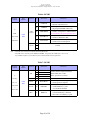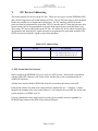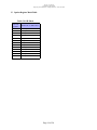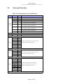
1
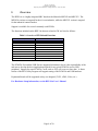
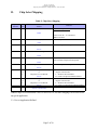
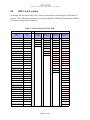
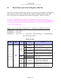
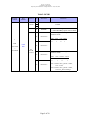
rpxl_fw_cw_basic.fm
Programmer’s/FW Manual
Proprietary and Confidential - All Rights Reserved - 1998, 1999, 2000
Embedded Planet, LLC (3Jan00)
RPX Lite Programmer’s/FW Manual - For Rev CW boards
Programming and FW Requirements for the RPXL
This document contains confidential information and is intended for the sole purpose of the end user to develop
applications on the RPX Lite product offered by Embedded Planet. Neither the document, nor reproductions of it, nor
information derived from it is to be given to others, nor used for any other purpose other than for RPX Lite
applications. No use is to be made of it which is or may be injurious to Embedded Planet and no use is to be made of it
other than for RPX Lite applications.
Revision Control:
15SEP99
First Release.
Table of Contents
I.
Overview . . . . . . . . . . . . . . . . . . . . . . . . . . . . . . . . . . . . . . . . . . 4
II.
Chip Select Mapping . . . . . . . . . . . . . . . . . . . . . . . . . . . . . . . . . 5
III.
BSP Code Location . . . . . . . . . . . . . . . . . . . . . . . . . . . . . . . . . . 6
IV.
Board Status and Control Registers (BSCRs) . . . . . . . . . . . . . . 8
V.
I2C Devices/Addressing . . . . . . . . . . . . . . . . . . . . . . . . . . . . . 11
A.
B.
C.
D.
E.
VI.
SEP Format/Interface Structure . . . . . . . . . . . . . . . . . . . . . . . . . . 11
STTM Format/Interface Structure . . . . . . . . . . . . . . . . . . . . . . . . 12
System Integration Timers . . . . . . . . . . . . . . . . . . . . . . . . . . . . . . 13
PCMCIA Control Registers . . . . . . . . . . . . . . . . . . . . . . . . . . . . . 13
Option Register Mask Table . . . . . . . . . . . . . . . . . . . . . . . . . . . . . 14
Interrupt Structure . . . . . . . . . . . . . . . . . . . . . . . . . . . . . . . . . . 15
VII. Processor Pin Assignments . . . . . . . . . . . . . . . . . . . . . . . . . . . 16
A.
B.
C.
Bus Interface Pins . . . . . . . . . . . . . . . . . . . . . . . . . . . . . . . . . . . . . 16
PCMCIA Interface Pins . . . . . . . . . . . . . . . . . . . . . . . . . . . . . . . . 17
I/O Port Interface Pins . . . . . . . . . . . . . . . . . . . . . . . . . . . . . . . . . 18
VIII. Performance . . . . . . . . . . . . . . . . . . . . . . . . . . . . . . . . . . . . . . . 19
A.
B.
@ 20 or 25MHZ . . . . . . . . . . . . . . . . . . . . . . . . . . . . . . . . . . . . . . 19
@ 33MHZ . . . . . . . . . . . . . . . . . . . . . . . . . . . . . . . . . . . . . . . . . . . 19
Page 1 of 20
rpxl_fw_cw_basic.fm
Programmer’s/FW Manual
Proprietary and Confidential - All Rights Reserved - 1998, 1999, 2000
C.
D.
E.
F.
@ 40MHZ . . . . . . . . . . . . . . . . . . . . . . . . . . . . . . . . . . . . . . . . . . . 19
@ 50MHZ . . . . . . . . . . . . . . . . . . . . . . . . . . . . . . . . . . . . . . . . . . . 19
@ 66MHZ . . . . . . . . . . . . . . . . . . . . . . . . . . . . . . . . . . . . . . . . . . . 20
@ 81MHZ . . . . . . . . . . . . . . . . . . . . . . . . . . . . . . . . . . . . . . . . . . . 20
Page 2 of 20
rpxl_fw_cw_basic.fm
Programmer’s/FW Manual
Proprietary and Confidential - All Rights Reserved - 1998, 1999, 2000
List of Tables
Overview of FW Related Functions . . . . . . . . . . . . . . . . . . . . . . . . . . . . . . . . . . . 4
Chip Select Mapping . . . . . . . . . . . . . . . . . . . . . . . . . . . . . . . . . . . . . . . . . . . . . . . 5
Code Location in x32 FLASH . . . . . . . . . . . . . . . . . . . . . . . . . . . . . . . . . . . . . . . . 6
BCSR0 . . . . . . . . . . . . . . . . . . . . . . . . . . . . . . . . . . . . . . . . . . . . . . . . . . . . . . . . . . 8
BCSR1 . . . . . . . . . . . . . . . . . . . . . . . . . . . . . . . . . . . . . . . . . . . . . . . . . . . . . . . . . . 9
BCSR2 . . . . . . . . . . . . . . . . . . . . . . . . . . . . . . . . . . . . . . . . . . . . . . . . . . . . . . . . . 10
BCSR3 . . . . . . . . . . . . . . . . . . . . . . . . . . . . . . . . . . . . . . . . . . . . . . . . . . . . . . . . . 10
I2C Address Map . . . . . . . . . . . . . . . . . . . . . . . . . . . . . . . . . . . . . . . . . . . . . . . . . 11
TBSCR, RTCSC, and PISCR . . . . . . . . . . . . . . . . . . . . . . . . . . . . . . . . . . . . . . . 13
PGCRA and PGCRB . . . . . . . . . . . . . . . . . . . . . . . . . . . . . . . . . . . . . . . . . . . . . . 13
OR Mask . . . . . . . . . . . . . . . . . . . . . . . . . . . . . . . . . . . . . . . . . . . . . . . . . . . . . . . 14
Interrupt Structure for the RPX Lite . . . . . . . . . . . . . . . . . . . . . . . . . . . . . . . . . . 15
Bus Interface - Multiple Function Pins . . . . . . . . . . . . . . . . . . . . . . . . . . . . . . . . 16
PCMCIA - Multiple Function Pins . . . . . . . . . . . . . . . . . . . . . . . . . . . . . . . . . . . 17
Page 3 of 20
rpxl_fw_cw_basic.fm
Programmer’s/FW Manual
Proprietary and Confidential - All Rights Reserved - 1998, 1999, 2000
I.
Overview
The RPX Lite is a highly integrated SBC based on the Motorola MPC850 and MPC823. The
MPC850 versions are targeted for the tel-com industries, while the MPC823 version is targeted
for the industrial controls market.
Support is available for several commonly used RTOSs.
The functions included on the RPX Lite that are related to FW are listed as follows:
Table 1: Overview of FW Related Functions
Entity
Function
Processor
DRAM
FLASH
NVRAM
10Base-T Ethernet
Monitor Port
Serial EEPROM
Serial Temp & Thermal Monitor
BCSR
MPC850 (SR, DC, DH, etc.) or MPC823
4MB or 16MB
2MB, 4MB, 8MB, or 16MB
0KB, 32KB, 128KB, 512KB
SCC2
SMC1
I2C
I2C
BCSR0, 1, 2, and 3
The PCMCIA Port and the USB Port are supported in hardware, but it is the responsibility of the
end user to develop the driver/application required for any given PCMCIA card or USB
peripheral. Support for some PCMCIA Cards, such as ATA, will occur at a later date. A future
release of the RPX Utility Program will support testing of the PCMCIA and USB hardware.
Expansion Boards will be supported as they are designed (T1/E1, xDSL, Video, etc.)
For Hardware Setup information, see the RPX Lite User’s Manual
Page 4 of 20
rpxl_fw_cw_basic.fm
Programmer’s/FW Manual
Proprietary and Confidential - All Rights Reserved - 1998, 1999, 2000
II.
Chip Select Mapping
Table 2: Chip Select Mapping
Chip Select
Number
Port
Size
Function/
Address
CS0#
x32
FLASH (x32)
Comment
Reset Vector @ IP = ‘0’:
FFF0 0000
FE00
DRAM (x32)
Vector set at IP = ‘0’ in hardware
BR0 set at FE00
4 or 16MBytes
CS2#
0000
Expansion Header
Routed to Expansion Receptacle
CS3#
x32
UUUU
Control & Status Registers
CS4#
x8
FA40
NVRAM or SRAM
CS1#
x32
FA00
Expansion Header
CS5#
CS6#
x16
or
U
CS7#
x16
or
U
IMMR
x32
UUUU
PCMCIA Slot B Chip Select Even Bytes
or
Chip Select 6 to I/O Header
UUUU
PCMCIA Slot B Chip Select Odd Bytes
or
Chip Select 7 to I/O Header
UUUU
Value at reset = FF00 0000,
then set to FA20 0000
Byte and/or word accessible.
0K, 32K, 128K, or 512KBytes
Also available at Expansion Receptacle
Routed to Expansion Receptacle
1) OP2 in MPC850 PCMCIA Control
Register selects mode:
L = PCMCIA Slot B enabled
H = CS6# to Expansion Header Enabled
1) OP2 in MPC850 PCMCIA Control
Register selects mode:
L = PCMCIA Slot B enabled
H = CS7# to I/O Expansion Header Enabled
Address maps are recommended values for the RPX Lite, but other mappings can be utilized for
any given application.
U = User or Application Defined
Page 5 of 20
rpxl_fw_cw_basic.fm
Programmer’s/FW Manual
Proprietary and Confidential - All Rights Reserved - 1998, 1999, 2000
III.
BSP Code Location
At start-up, the code for the RPX Lite is always located in the second to highest 512K block of
memory. This 512K block of memory is reserved for the BSP or RTOS (FLASH intensive RTOSs
will require a larger block of memory).
Table 3: Code Location in x32 FLASH
FLASH Memory Option
Address
Range
Block
Size
2MByte
29LV400
4MBytes
29LV800
8MBytes
29LV160
16MBytes
29LV320
FFFF FFFF - FFF8 0000
512KB
512KB
512KB
512KB
512KB
512KB
512KB
512KB
512KB
512KB
512KB
512KB
512KB
512KB
512KB
512KB
512KB
512KB
512KB
512KB
512KB
512KB
512KB
512KB
512KB
512KB
512KB
512KB
512KB
512KB
512KB
512KB
User
BSP
User
BSP
User
BSP
User
BSP
FFF7 FFFF - FFF0 0000
FFEF FFFF - FFE8 0000
FFE7 FFFF - FFE0 0000
FFDF FFFF - FFD8 0000
FFD7 FFFF - FFD0 0000
FFCF FFFF - FFC8 0000
FFC7 FFFF - FFC0 0000
FFBF FFFF - FFB8 0000
FFB7 FFFF - FFB0 0000
FFAF FFFF - FFA8 0000
FFA7 FFFF - FFA0 0000
FF9F FFFF - FF98 0000
FF97 FFFF - FF90 0000
FF8F FFFF - FF88 0000
FF87 FFFF - FF80 0000
FF7F FFFF - FF78 0000
FF77 FFFF - FF70 0000
FF6F FFFF - FF68 0000
FF67 FFFF - FF60 0000
FF5F FFFF - FF58 0000
FF57 FFFF - FF50 0000
FF4F FFFF - FF48 0000
FF47 FFFF - FF40 0000
FF3F FFFF - FF38 0000
FF37 FFFF - FF30 0000
FF2F FFFF - FF28 0000
FF27 FFFF - FF20 0000
FF1F FFFF - FF18 0000
FF17 FFFF - FF10 0000
FF0F FFFF - FF08 0000
FF07 FFFF - FF00 0000
Page 6 of 20
rpxl_fw_cw_basic.fm
Programmer’s/FW Manual
Proprietary and Confidential - All Rights Reserved - 1998, 1999, 2000
1)
Reset vector @ FFF0 0100 but for A[0:3 4:7 8:11]:
A(0:10) = X for 2MBytes
A(0:9) = X for 4MBytes
A(0:8) = X for 8MBytes
A(0:7) = X for 16MBytes
where X = “don’t’ care” (i.e. the address lines defined by “X” are not connected to the FLASH memory)
2)
The actual on-board FLASH memory size is mirrored throughout the entire address space
(excluding internal processor address spaces) until OR0 is written.
3)
Flash base address is remapped to FE00 0000 when BR0/OR0 is written.
Page 7 of 20
rpxl_fw_cw_basic.fm
Programmer’s/FW Manual
Proprietary and Confidential - All Rights Reserved - 1998, 1999, 2000
IV.
Board Status and Control Registers (BSCRs)
There exists on-board control and status registers. These registers are configured as a x32 port and
can be accessed via byte, word, or longword. The registers are defined as shown in the Table
below. All registers are read modify write capable (except register 3 which is read only).
Upon power-up (HRESET#) the default value configured in the registers, after masking
(“anding”) with FF 1F F8 FF, is longword 3E 00 80 UU (i.e. if the first access to the BCSR after
reset is a longword read, the value read, after masking with FF 1F F8 FF will be 3E 00 80 UU,
where UU is as defined below).
Register values at reset (values in binary and “x” = undefined or determined by function):
R/W Register 0 = 0011 1110
R/W Register 1 = xxx0 0000
R/W Register 2 = 1000 0xxx
RO Register 3 = xxxx 11xx (UU = first four bits = dipswitch setting, 1, 1, NVRAM Battery
status, RTC Battery Status)
Table 4: BCSR0
Register
Number
Byte
Address
Function
Ethernet
XCVR
Control
Bit
Mnemonic
0
ETHEN
1
ETHLPBK
2
COLTEST#
3
FULLDPLX#
4
5
LED4
LED5
0
R/W
reset value
=
0011 1110
FA40
0000
LEDS
CS4#
Control
6
ENNVRAM
Monitor
XVCR
Control
7
ENMONXCVR
Page 8 of 20
Definition
0 = Disable Transceiver
1 = Enable Transceiver
0 = Disable Transceiver Loop Back Test
1 = Enable Transceiver Loop Back Test
0 = Enable collision testing on Transceiver
1 = Disable collision testing on Transceiver
0 = Enable full duplex mode of operation
1 = Disable full duplex mode of operation
0 = LED “on”
1 = LED “off”
0 = Disable on-board NVRAM and
Enable CS4# at I/O Receptacle
1 = Enable on-board NVRAM and
Disable CS4# at I/O Receptacle
0 = Disable Monitor Port Transceiver
1 = Enable Monitor Port Transceiver
rpxl_fw_cw_basic.fm
Programmer’s/FW Manual
Proprietary and Confidential - All Rights Reserved - 1998, 1999, 2000
Table 5: BCSR1
Register
Number
Byte
Address
Function
Bit
Unused
8
9
10
Mnemonic
Definition
Unused
11
IPB5SEL
12
PCVCTL4
0 = BVD2/SPKR signal routed to IPB5
1 = INPACK#/DREQ signal routed to IPB5
Defines VCC_SLOT voltage on
PCMCIA Slot B:
GND +5.0V +3.3V GND
0
0
1
1
0
1
0
1
1
R/W
reset value
=
xxx0 0000
FA40
0001
13
PCVCTL5
PC
Slot B
Control
Defines VPP_SLOT voltage on
PCMCIA Slot B:
14
PCVCTL6
GND
0
0
15
PCVCTL7
Page 9 of 20
Note 1 Note 2
0
1
1
0
HI-Z
1
1
Note 1: Hi-Z if VCC_SLOT = GND,
else +12.0V.
Note 2: Hi-Z if VCC_SLOT = GND,
else VCC_SLOT Voltage
rpxl_fw_cw_basic.fm
Programmer’s/FW Manual
Proprietary and Confidential - All Rights Reserved - 1998, 1999, 2000
Table 6: BCSR2
Register
Number
Byte
Address
Function
Bit
Mnemonic
16
USBSUSP
17
USBSPD
18
USBPWREN
19
ENUSBCLK
20
ENPA5HDR
2
R/W
reset value
=
1000 0xxx
USB
Control
FA40
0002
Unused
21
22
23
Definition
0 = Enable USB Transceiver
1 = Disable USB Transceiver
0 = Low Speed (6MHZ USB clock)
1 = High Speed (48MHZ USB clock)
0 = Disable +5.0V power to USB connector
1 = Enable +5.0V power to USB connector
- do not enable if 3V power option is used
0 = Disable USB clock to PA5
1 = Enable USB clock to PA5
0 = Disable PA5 at P2 Receptacle
1 = Enable PA5 at P2 Receptacle
Unused
Note: - The USB clock can be fed to both PA5 and the P2 Receptacle.
- The USB clock is currently set for 6MHZ and 48MHZ. Via special, this “USB Clock” can be set to
any realizable frequency as provided for by the on-board CY2071A clock synthesizer.
Table 7: BCSR3
Register
Number
Byte
Address
Function
Bit
Mnemonic
24
25
26
27
28
D24
D25
D26
D27
RPXL
Flash
29
RDY/BSY#
Nvram
30
BWNVR#
RTC
31
BWRTC#
SW
3
R only
W = xx
reset value
=
xxxx 11xx
FA40
0003
Page 10 of 20
Definition
D(2427) defines DipSwitch Settings
(D24 is MSb, D27 is LSb)
(D24 = position 0 on switch)
Reserved (reads back ‘1’)
0 = Flash operation executing and busy
1 = Flash operation complete
0 = NVRAM Battery is low
1 = NVRAM Battery is good
or no NVRAM installed
0 = Real Time Clock Battery is low or
no External Battery is attached
1 = Real Time Clock Battery is good
rpxl_fw_cw_basic.fm
Programmer’s/FW Manual
Proprietary and Confidential - All Rights Reserved - 1998, 1999, 2000
V.
I2C Devices/Addressing
The board contains two devices on the I2C bus. These two devices are a Serial EEPROM (SEP)
and a Serial Temperature & Thermal Monitor (STTM). The I2C bus also routes to the Expansion
Header for possible use on Expansion board designs. The I2C interface pin SDA from the
processor must be programmed as open drain. The I2C interface pin SCL from the processor does
not necessarily have to be programmed as an open drain signal, because presently there are no
other master I2C devices that reside on the I2C bus. If a master I2C device where designed onto
an expansion card, then the SCL signal must also be programmed for open drain operation. The
RPX Lite board sets both I2C signals to open drain operation.
Table 8: I2C Address Map
Device
Function
I2C Addressing
SEP
Configuration Information
STTM
Serial Temperature and Thermal Monitor
A8h - A9h for 1K/2K devices (128/256 x 8)
A8h - ABh for 4K device (512 x 8)
A8h - AFh for 8K device (1K x 8)
90h - 91h (8 bytes in device)
A. SEP Format/Interface Structure
Data is stored in the EEPROM device as a series of ASCII records. Each record is terminated
with the NEWLINE character (ASCII hex 0x0A), and the last record is terminated with two
NEWLINE characters.
All data bytes after the double NEWLINE of the last record have the binary value 0xFF.
Each record consists of a name and a value which are separated by an ‘=’ character. A name
identifies the meaning of the value which follows it. For example, the record HZ=50 declares the
system frequency (in MHZ) to be 50.
For more information on the names used in records, please read the section or appendix on
EEPROM data formats in the RPX Utility Software Manual.
Page 11 of 20
rpxl_fw_cw_basic.fm
Programmer’s/FW Manual
Proprietary and Confidential - All Rights Reserved - 1998, 1999, 2000
B. STTM Format/Interface Structure
The driver for the STTM sets the interrupt out for low true operation. Interrupt mode is selected
but is not enabled at the processor (IRQ1#). The driver returns the temperature of the device and
also a calibrated temperature for reporting ambient air temperature. The calibration parameter is
programmed into the SEP and is used to extrapolate ambient air temperature.
Page 12 of 20
rpxl_fw_cw_basic.fm
Programmer’s/FW Manual
Proprietary and Confidential - All Rights Reserved - 1998, 1999, 2000
C. System Integration Timers
Table 9: TBSCR, RTCSC, and PISCR
Mnemonic
Internal Address
TBSCR
200
RTCSC
220
PISCR
240
Note:
Value = Bits 0-15
Default Value
VVC3
00C3
VVC1
00C1
VV83
0083
Function
VV = User Specified Interrupt Level
Time Base and Decrementer Enabled but Stopped on FRZ
VV = User Specified Interrupt Level
RTC Enabled but not stopped on FRZ
VV = User Specified Interrupt Level
Periodic Timer Enabled, but Stopped on FRZ and
Periodic Timer Interrupt Disable
These registers powered by the KAPWR pin (Battery Backed Circuits). They will only
be reset on POR (when battery voltage is not available or applied for the first time, and the
system powers up). The RPX Lite requires an external battery for back-up operation.
D. PCMCIA Control Registers
PCMCIA port A is not implemented on the MPC823 or MPC850 family.
Table 10: PGCRA and PGCRB
Mnemonic
Internal Address
PGCRA
PGCRB
0E0
0E4
Note:
Value - Bits 0-15
Default Value
Function
Reserved - not implemented in the MPC850/MPC823
VVLL 0080
VV = User Specified Interrupt Level for PCMCIA Card
LL = User Specified Interrupt Level for Status Change
0000 0080
Internal DMA request disabled
Buffers for Card B disabled ( OP2 deasserted) and
CS6#/CS7# valid at I/O Header
Reset signal active (OP3 asserted)
OP2 in PGCRB has a dual function in that it either enables the buffers for PCMCIA Slot
B or enables the buffers which allow the CS6# and CS7# signals to be active at the I/O
Header:
(If Bit 24 = CBOE = 0 then PCMCIA Slot B Buffers Enabled and
CS6#/CS7# not active at I/O Header)
(If Bit 24 = CBOE = 1 then PCMCIA Slot B Buffers Disabled and
CS6#/CS7# active at I/O Header)
Page 13 of 20
rpxl_fw_cw_basic.fm
Programmer’s/FW Manual
Proprietary and Confidential - All Rights Reserved - 1998, 1999, 2000
E. Option Register Mask Table
Table 11: OR Mask
A(0:12)
in OR’s
“mmmm m” in Table above
F800 0
FC00 0
FE00 0
FF00 0
FF80 0
FFC0 0
FFE0 0
FFF0 0
FFF8 0
FFFC 0
FFFE 0
FFFF 0
FFFF 8
128MBytes
64MBytes
32MBytes
16MBytes
8MBytes
4MBytes
2MBytes
1MByte
512KBytes
256KBytes
128KBytes
64KBytes
32KBytes
Page 14 of 20
rpxl_fw_cw_basic.fm
Programmer’s/FW Manual
Proprietary and Confidential - All Rights Reserved - 1998, 1999, 2000
VI.
Interrupt Structure
Table 12: Interrupt Structure for the RPX Lite
Entity
External
Interrupt
Interrupt
Code
IRQ0#
IRQ1#
IRQ2#
IRQ3#
00
08
10
18
IRQ4#
20
IRQ5#
28
IRQ6#
30
IRQ7#
38
NMI
Internal
Level 0
Level 1
Level 2
Level 3
Level 4
Level 5
Level 6
Level 7
SIU
DEC
TB
PIT
RTC
PCMCIA
CPM
Port C Pins
SCC(1:4)
Timer(1:4)
DMA
RISC Timer
I2C
SPI
SMC1
SMC2
USB
Function
Power Fail
Temperature and Thermal Monitor (STTM)
Availability depends on configuration - On I/O Header
(pin multiplexes IRQ3# with DPAR0)
Availability depends on configuration - On I/O Header
(pin multiplexes IRQ4# with DPAR1)
Availability depends on configuration - On I/O Header
(pin multiplexes IRQ5# with DPAR2)
Availability depends on configuration - On I/O Header
(pin multiplexes IRQ6# with DPAR3)
From Header
From Watchdog Timer or IRQ0#
04
0C
14
1C
24
2C
34
3C
Routing from interrupt sources below. Actual
routings depended on application
Each source is software routed to any “Level”
(Each source has unique “vector”)
32 sources combined into one interrupt
which is software routed to any “Level”
(Each source has unique “vector”)
Page 15 of 20
rpxl_fw_cw_basic.fm
Programmer’s/FW Manual
Proprietary and Confidential - All Rights Reserved - 1998, 1999, 2000
VII.
Processor Pin Assignments
The following sections define the function that is associated with certain processor pins. Many of
the processor pins have multiple functions, most of which are programmable by the FW. This
section will detail the functionality associated with the respective processor pins, and must be
used by the firmware/software to correctly configure the system.
A. Bus Interface Pins
Table 13: Bus Interface - Multiple Function Pins
Defined Function
SIZ0/REG#
BDIP/GPLB51
SIZ0 and REG#
BDIP#
Unused
Y
Y
RSV#/IRQ2#1
IRQ2#
Unused
Y
KR#/RETRY#/IRQ4#/SPKROUT1
RETRY#
Unused
Y
IRQ(3:6)#
Can be redefined for DP(0:3) for an
Expansion Card that requires Parity.
Use IRQ7# or one of the Port C pins
for interrupt capability
Y
DP0/IRQ3#1
DP1/IRQ4#1
DP2/IRQ5#1
DP3/IRQ6#1
FRZ/IRQ6#1
CS6#/CE1B#
CS7#/CE2B#
GPLA0#
GPLA1#
FRZ
CS6# or CE1B#
CS7# or CE2B#
GPLA2#/CS2#1
GPLA3#
GPLA2#
N
See OP2 below
See OP2 below
UPM Output Enable
GPCM Output Enable
Only used at I/O Expansion Socket
Y
Y
Y
Y
Y
2
UPWAITA
Unused
Unused, Pulled-Down
Y
N
UPWAITB/GPLB4#2
GPLA5#
UPWAITB
Unused, Pulled-Down
N
ALEB/DSCK/AT13
ALEB
Unused
PCMCIA Slot B ALE signal
Y
N
OP2/MODCK1/STS#3
OP2
N
OP3/MODCK2/DSDO3
OP3
PCMCIA Slot B Buffer Enable
0 = Enable Buffers,
Disable CS6#/CS7# at I/O Header
1 = Disable Buffers,
Enable CS6#/CS7# at I/O Header
(MODCK1 @ reset rising = ‘0’)
PCMCIA Slot B Reset Signal
(MODCK2 @ reset rising = ‘0’)
UPWAITA/GPLA4#
1 Programmed
2 Programmed
3 Hard
Additional comments
At
Expansion
Socket
Processor Pin Name
in SIUMCR
in MAMR
Reset Configuration and SIUMCR
Page 16 of 20
N
rpxl_fw_cw_basic.fm
Programmer’s/FW Manual
Proprietary and Confidential - All Rights Reserved - 1998, 1999, 2000
B. PCMCIA Interface Pins
The hard reset word configures the following pins to function as PCMCIA signals.
Table 14: PCMCIA - Multiple Function Pins
Processor Pin
Name
PCMCIA
Function
IPB0
IPB1
IPB2
IPB3
IPB4
IPB5
VS1
VS2
WP or IOCS16# or DREQ#
CD2
CD1
BVD1 or SPKR or DREQ#
IPB6
IPB7
WAITB#
OP3
OP2
BVD2 or STSCHG
RDY or IRQ#
Wait States
Reset Signal
Buffer Enable/Disable
Control
Additional comments
At
Expansion
Socket
Function depends on memory or I/O Card
Function depends on memory or I/O Card
(see Note 1)
Function depends on memory or I/O Card
Function depends on memory or I/O Card
No
Used to enable or disable the on-board
buffers that isolate the PCMCIA bus from
the Processor bus.
&
CS6#/CS7#
Enable/Disable
Control
In addition, this signal also enables or disables
chip selects 6 and 7 from the I/O Header. When
the Buffers are enabled, CS6# and CS7# are
disabled. When the Buffers are disabled, CS6#
and CS7# are enabled.
Note 1: The PCMCIA signal INPACK# is not required by the MPC8XX, and as such, not
supported. Some PCMCIA type DMA cards route the DREQ signal on the INPACK#
pin. To support these cards, Control Register 2, bit 19, allows routing of the INPACK#
(DREQ) signal to IPB5.
Note 2: BCSR1, bits 12-15, also controls the operation of
the PCMCIA interface (voltages to socket).
Page 17 of 20
rpxl_fw_cw_basic.fm
Programmer’s/FW Manual
Proprietary and Confidential - All Rights Reserved - 1998, 1999, 2000
C. I/O Port Interface Pins
Refer to the pinouts document for pinout assignments.
3) Any of the port signals that are used for on-board functions can be used on an Expansion Card
if the respective on-board function is disabled (via the BCSRs).
4) Port C pins can also be defined as interrupt signals to the processor core. Each Port C pin that
is configured as an interrupt pin has a unique vector associated with it, and each pin can be
defined as edge or low level active. This allows Expansion Cards to use Port C pins as
interrupt lines to the processor if needed. Check the P1_P2.xls spreadsheet for available Port
C pins and also see note 3) above.
5) The I2C bus (PB26 and PB27 pins) is used on-board but also routed to the I/O
Header. See the I2C section above for used I2C addresses.
Page 18 of 20
rpxl_fw_cw_basic.fm
Programmer’s/FW Manual
Proprietary and Confidential - All Rights Reserved - 1998, 1999, 2000
VIII.
Performance
See “Clocks and Reset Registers” section for the exact frequency that processor is running at.
A. @ 20 or 25MHZ
Single Beat Read 3 clocks (1 wait states)
Single Beat Write 2 clocks (0 wait states)
Burst Read
7 clocks (1:1:2:1 cycle)
Burst Write
5 clocks (0:1:1:1 cycle)
Refresh
2 clocks
Back to Back Accesses, including refresh, have 1 clock between accesses
B. @ 33MHZ
Single Beat Read 3 clocks (1 wait states)
Single Beat Write 3 clocks (1 wait states)
Burst Read
9 clocks (1:2:2:2 cycle)
Burst Write
5 clocks (0:1:1:1 cycle)
Refresh
3 clocks
Back to Back Accesses, including refresh, have 1 clock between accesses
C. @ 40MHZ
Single Beat Read 4 clocks (2 wait states)
Single Beat Write 4 clocks (2 wait states)
Burst Read
10 clocks (2:2:2:2 cycle)
Burst Write
10 clocks (2:2:2:2 cycle)
Refresh
4 clocks
Back to Back Accesses, including refresh, have 1 clock between accesses
D. @ 50MHZ
Single Beat Read 5 clocks (3 wait states)
Single Beat Write 5 clocks (3 wait states)
Burst Read
11 clocks (3:2:2:2 cycle)
Burst Write
10 clocks (3:2:2:1 cycle)
Refresh
5 clocks
Back to Back Accesses, including refresh, have 1 clock between accesses
Page 19 of 20
rpxl_fw_cw_basic.fm
Programmer’s/FW Manual
Proprietary and Confidential - All Rights Reserved - 1998, 1999, 2000
E. @ 66MHZ
Single Beat Read 6 clocks (2 wait states)
Single Beat Write 6 clocks (2 wait states)
Burst Read
18 clocks (2:4:4:4 cycle)
Burst Write
10 clocks (1:2:2:2 cycle)
Refresh
6 clocks
Back to Back Accesses, including refresh, have 2 clocks between accesses
F. @ 81MHZ
Single Beat Read 8 clocks (4 wait states)
Single Beat Write 8 clocks (4 wait states)
Burst Read
20 clocks (4:4:4:4 cycle)
Burst Write
20 clocks (4:4:4:4 cycle)
Refresh
8 clocks
Back to Back Accesses, including refresh, have 2 clocks between accesses
Page 20 of 20