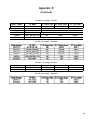
1
Distributed Power System
SD3000 Drive Configuration
and Programming
Instruction Manual S-3006-1
r
RELIANCE
ELECTRIC Cl
The information in the user’s manual is subject to change without notice.
ONLY QUALlFlED ELECTRICAL PERSONNEL FAMILIAR WITH THE CONSTRUCTION
OPERATION OF THIS EQUIPMENT AND THE HAZARDS INVOLVED SHOULD INSTALL, ADJUST,
OPERATE, OR SERVICE THIS EQUIPMENT. READ AND UNDERSTAND THIS MANUAL AND OTHER
APPLICABLE MANUALS IN THEIR ENTIRETY BEFORE PROCEEDING. FAILURE TO OBSERVE THIS
PRECAUTION COULD RESULT IN SEVERE BODILY INJURY OR LOSS OF LIFE.
WARNING
THE USER MUST PROVIDE AN EXTERNAL, HARDWIRED EMERGENCY STOP CIRCUIT OUTSIDE OF
THE CONTROLLER CIRCUITRY THIS CIRCUIT MUST DISABLE THE SYSTEM IN CASE OF
IMPROPER OPERATION. UNCONTROLLED MACHINE OPERATION MAY RESULT IF THIS
PROCEDURE IS NOT FOLLOWED. FAILURE TO OBSERVE THIS PRECAUTION COULD RESULT IN
BODILY INJURY
I
WARNING
I
ONLY QUALIFIED RELIANCE PERSONNEL OR OTHER TRAINED PERSONNEL WHO UNDERSTAND
THE POTENTIAL HAZARDS INVOLVED MAY MAKE MODIFICATIONS TO THE RACK
CONFIGURATION, VARIABLE CONFIGURATION, AND APPLICATION TASKS. ANY MODIFICATIONS
MAY RESULT IN UNCONTROLLED MACHINE OPERATION. FAILURE TO OBSERVE THESE
PRECAUTIONS COULD RESULT IN DAMAGE TO EQUIPMENT AND BODILY INJURY.
I
WARNING
REGISTERS AND BITS IN THE UDC MODULE THAT ARE DESCRIBED AS “READ ONLY” OR FOR
“SYSTEM USE ONLY” MUST NOT BE WRITTEN TO BY THE USER. WRITING TO THESE REGISTERS
AND BITS MAY RESULT IN IMPROPER SYSTEM OPERATION. FAILURE TO OBSERVE THIS
PRECAUTION COULD RESULT IN BODILY INJURY
CAUTION: Electronic motor overload protection must be provided for each motor in a Distributed Power
drive application to protect the motor against excessive heat caused by high currents. This protection can be
provided by either the THERMAL OVERLOAD software block or an external hardware device. Applications in
which a single power module is controlling multiple motors cannot use the THERMAL OVERLOAD software
block and must use an external hardware device or devices to provide this protection. Failure to observe this
precaution could result in damage to, or destruction of, the equipment.
EthernetTM is a trademark of Xerox Corporation.
WindowsTM I’S a trademark of Microsoft Corporation.
ReSourceTM ’IS a trademark of Reliance Electric Company or its subsidiaries.
Reliance* and AutoMax@ are registered trademarks of Reliance Electric Company or its subsidiaries.
0
Copyright Reliance Electric Industrial Company 1995.
I
Table of Contents
1 .O Introduction . . . . . ..................................................................
2.0
3.0
1 .1 Related Publications . . . . . . . . . . . . . . . . . . . . . . . . . . . . . . . . . . . . . . . . . . . . . . . . . . . . . . . . . . . . . .
l-l
Configuring the UDC Module, Regulator Type, and Parameters . . . . . . . . . . . . . . . . . . . . . . . . .
2-1
2.1 Adding a UDC Module . . . . . . . . . . . . . . . . . . . . . . . . . . . . . . . . . . . . . . . . . . . . . . . . . . . . . . . . . . . . .
2.1 .1 Rules for Configuring/Selecting Drives for the UDC Module . . . . . . . . . . . . . . . . . . . . . . .
2.2 Entering the Drive Parameters . . . . . . . . . . . . . . . . . . . . . . . . . . . . . . . . . . . . . . . . . . . . . . . . . . . . . .
2.2.1 Armature Power Module Data Screen . . . . . . . . . . . . . . . . . . . . . . . . . . . . . . . . . . . . . . . . . .
2.2.2 Field Power Module Data Screen . . . . . . . . . . . . . . . . . . . . . . . . . . . . . . . . . . . . . . . . . . . . . .
2.2.3 Speed Feedback Data Screen . . . . . . . . . . . . . . . . . . . . . . . . . . . . . . . . . . . . . . . . . . . . . . . . .
2.2.4 Meter Port Selection Screen . . . . . . . . . . . . . . . . . . . . . . . . . . . . . . . . . . . . . . . . . . . . . . . . . . .
2.3 Generating the Drive Parameter Files and Printing Drive Parameters . . . . . . . . . . . . . . . . . . . . .
2-1
2-2
2-2
2-4
2-6
2-7
2-10
2-12
Configuring the UDC Module’s Registers . . . . . . . . . . . . . . . . . . . . . . . . . . . . . . . . . . . . . . . . . . . . . .
3-1
3.1
3.2
3.3
3.4
3.5
Rail l/O Port Registers (Registers O-23) . . . . . . . . . . . . . . . . . . . . . . . . . . . . . . . . . . . . . . . . . . . . . .
UDC/PMI Communication Status Registers (Registers 80-89/1080-1 089) . . . . . . . . . . . . . . . . .
Command Registers (Registers 100-1 99/1100-1199) . . . . . . . . . . . . . . . . . . . . . . . . . . . . . . . . . .
Feedback Registers (Registers 200-299,1200-1299)
..................................
Application Registers (Registers 300599, Every Scan)
(Registers 1300-I 599, Every Nth Scan) . . . . . . . . . . . . . . . . . . . . . . . . . . . . . . . . . . . . . . . . . . . . . .
3.6 UDC Module Test I/O Registers (Registers 1000-l 017) . . . . . . . . . . . . . . . . . . . . . . . . . . . . . . . . .
3.6.1 UDC Module Test Switch Inputs Register (Register 1000) . . . . . . . . . . . . . . . . . . . . . . . . .
3.6.2 UDC Module Meter Port Setup Registers (Registers 1001-I 017) . . . . . . . . . . . . . . . . . . .
3.6.2.1 Resolution of Meter Port Data . . . . . . . . . . . . . . . . . . . . . . . . . . . . . . . . . . . . . . . . . .
3.7 Interrupt Status and Control Registers (Registers 2000-2047) . . . . . . . . . . . . . . . . . . . . . . . . . . .
4.0
l-l
3-4
3-6
3-l 4
3-21
3-38
3-40
3-40
3-42
3-42
3-48
Application Programming for DPS Drive Control . . . . . . . . . . . . . . . . . . . . . . . . . . . . . . . . . . . . . . .
4-1
4.1 AutoMaxTasks . . . . . . . . . . . . . . . . . . . . . . . . . . . . . . . . . . . . . . . . . . . . . . . . . . . . . . . . . . . . . . . . . . .
4.2 UDCTasks . . . . . . . . . . . . . . . . . . . . . . . . . . . . . . . . . . . . . . . . . . . . . . . . . . . . . . . . . . . . . . . . . . . . . . .
4.2.1 Typical Structure of a UDC Task . . . . . . . . . . . . . . . . . . . . . . . . . . . . . . . . . . . . . . . . . . . . . . .
4.2.2 Local Tunable Variables . . . . . . . . . . . . . . . . . . . . . . . . . . . . . . . . . . . . . . . . . . . . . . . . . . . . . .
4.2.2.1 Calculating Local Tunable Values . . . . . . . . . . . . . . . . . . . . . . . . . . . . . . . . . . . . . . .
4.2.3 UDC/PMITaskCommunication . . . . . . . . . . . . . . . . . . . . . . . . . . . . . . . . . . . . . . . . . . . . . . . .
4.3 AutoMax Processor Task and UDC Task Coordination . . . . . . . . . . . . . . . . . . . . . . . . . . . . . . . . .
4-1
4-1
43
4-5
4-5
4-6
4-9
5.0 On-Line Operation . . . . . . . . . . . . . . . . . . . . . . . . . . . . . . . . . . . . . . . . . . . . . . . . . . . . . . . . . . . . . . . . . . .
5.1
5.2
5.3
5.4
Loading the UDC Module’s Operating System . . . . . . . . . . . . . . . . . . . . . . . . . . . . . . . . . . . . . . . .
Loading the Drive Parameters and UDC Tasks . . . . . . . . . . . . . . . . . . . . . . . . . . . . . . . . . . . . . . . .
Running, Stopping, and Deleting UDC Application Tasks . . . . . . . . . . . . . . . . . . . . . . . . . . . . . . .
UDC Information Log and Error Log . . . . . . . . . . . . . . . . . . . . . . . . . . . . . . . . . . . . . . . . . . . . . . . . .
5-I
5-l
5-I
5-2
5-2
Appendices
Appendix A
SD3000 Drive Register Reference . . . . . . . . . . . . . . . . . . . . . . . . . . . . . . . . . . . . . . . . . . . . . . . . . . . . . . . .
A-l
Appendix B
SD3000 Local Tunable Variables . . . . . . . . . . . . . . . . . . . . . . . . . . . . . . . . . . . . . . . . . . . . . . . . . . . . . . . . .
B-l
Appendix C
SD3000 Control Algorithm . . . . . . . . . . . . . . . . . . . . . . . . . . . . . . . . . . . . . . . . . . . . . . . . . . . . . . . . . . . . . . .
SD3000 Armature Current Regulation Algorithm . . . . . . . . . . . . . . . . . . . . . . . . . . . . . . . . . . . . . . . . . . . .
SD3000 Field Current Regulation Algorithm . . . . . . . . . . . . . . . . . . . . . . . . . . . . . . . . . . . . . . . . . . . . . . .
C-l
C-2
C-3
Appendix D
Status of Data in the AutoMax Rack after a STOP-ALL Command or STOP-ALL Fault . . . . . . . . . . .
D-l
Appendix E
Power Module Model Numbers and Parameter Default Values . . . . . . . . . . . . . . . . . . . . . . . . . . . . . . .
E-l
Appendix F
Armature Current Feedback Resolution . . . . . . . . . . . . . . . . . . . . . . . . . . . . . . . . . . . . . . . . . . . . . . . . . . .
F-l
Appendix G
Drive Control Register Operating States . . . . . . . . . . . . . . . . . . . . . . . . . . . . . . . . . . . . . . . . . . . . . . . . . . .
G-l
Appendix H
Field Current Regulation Algorithm with Field Weakening Turned Off . . . . . . . . . . . . . . . . . . . . . . . . . . H-l
Appendix I
Instantaneous Overcurrent Trip Point . . . . . . . . . . . . . . . . . . . . . . . . . . . . . . . . . . . . . . . . . . . . . . . . . . . . .
I-1
Appendix J
D-C Amp Rating Parameter Precautions . . . . . . . . . . . . . . . . . . . . . . . . . . . . . . . . . . . . . . . . . . . . . . . . . . .
J-l
List of Figures
Figure 2.1 - SD3000 Drive Parameter Entry Screen . . . . . . . . . . . . . . . . . . . . . . . . . . . . . . . . . . . . . . . . . . . . . .
2-3
Figure 2.2 - Armature Power Module Parameter Entry Screen . . . . . . . . . . . . . . . . . . . . . . . . . . . . . . . . . . . . .
Figure 2.3 - l-Phase Field Power Module Parameter Entry Screen . . . . . . . . . . . . . . . . . . . . . . . . . . . . . . . . .
2-4
2-6
Figure 2.4 - Speed Feedback Parameter Entry Screen With No Feedback Device Selected . . . . . . . . . . . 2-8
Figure 2.5 - Speed Feedback Parameter Entry Screen With A Resolver Selected . . . . . . . . . . . . . . . . . . . . 2-8
Figure 2.6 - Speed Feedback Parameter Entry Screen With An Analog Tachometer Selected . . . . . . . . . 2-9
2-l 0
Figure 2.7 - Meter Port Selection Entry Screen . . . . . . . . . . . . . . . . . . . . . . . . . . . . . . . . . . . . . . . . . . . . . . . . . .
Figure 2.8 - PMI Meter Port Parameters - SD3000 . . . . . . . . . . . . . . . . . . . . . . . . . . . . . . . . . . . . . . . . . . . . . . . .
2-l 1
Figure 3.1 - Typical UDC Task Scan . . . . . . . . . . . . . . . . . . . . . . . . . . . . . . . . . . . . . . . . . . . . . . . . . . . . . . . . . . . .
Figure 3.2 - Nth Scan Interrupts . . . . . . . . . . . . . . . . . . . . . . . . . . . . . . . . . . . . . . . . . . . . . . . . . . . . . . . . . . . . . . .
3-38
3-39
Figure 4.1 - Typical UDC Task Scan . . . . . . . . . . . . . . . . . . . . . . . . . . . . . . . . . . . . . . . . . . . . . . . . . . . . . . . . . . . .
4-2
Figure 4.2 - Data/Time Flow for UDC Module and PMI . . . . . . . . . . . . . . . . . . . . . . . . . . . . . . . . . . . . . . . . . . .
4-8
Figure 4.3 - Nth Scan Interrupts . . . . . . . . . . . . . . . . . . . . . . . . . . . . . . . . . . . . . . . . . . . . . . . . . . . . . . . . . . . . . . .
4-10
List of Tables
Table 3.1 - UDC Module Configuration Views and Registers . . . . . . . . . . . . . . . . . . . . . . . . . . . . . . . . . . . . . . 3-2
Table 3.2 - UDC Module Dual Port Memory Register Organization . . . . . . . . . . . . . . . . . . . . . . . . . . . . . . . . . 3-3
Table 3.3 - Rail l/O Port Registers . . . . . . . . . . . . . . . . . . . . . . . . . . . . . . . . . . . . . . . . . . . . . . . . . . . . . . . . . . . . . 3-4
Table 3.4 - Fault Register and Check Bit Fault Counter Register Usage
for a Digital I/O Rail or 4-Output Analog Rail Module . . . . . . . . . . . . . . . . . . . . . . . . . . . . . . . . . . . 3-5
Table 3.5 - Fault Register and Check Bit Fault Counter Register Usage
for a 4-Input Analog Rail Module . . . . . . . . . . . . . . . . . . . . . . . . . . . . . . . . . . . . . . . . . . . . . . . . . . . . 3-5
Table 3.6 - Fault Register and Check Bit Fault Counter Register
Usage for a 2-Output/2-Input
Analog Rail Module . . . . . . . . . . . . . . . . . . . . . . . . . . . . . . . . . . . . . 3-6
Table 3.7 - UDC Module Meter Port Setup Registers . . . . . . . . . . . . . . . . . . . . . . . . . . . . . . . . . . . . . . . . . . . . . 3-42
Ill
1 .0 INTRODUCTlON
The products described in this manual are manufactured or distributed by Reliance Electric Industrial
Company.
Distributed Power System (DPS) drives are controlled through coordination between:
l
Tasks written by the programmer for the AutoMax@ Processor
l
Tasks written by the programmer for the Universal Drive Controller (UDC) module
l
The control algorithm and a number of software routines executed by the Power Module Interface
PMI
The data and commands required by the PMI operating system to carry out its functions are provided
by the programmer through the AutoMax rack configuration and the UDC task. The programmer
provides this information by:
l
Entering the drive parameters
l
Configuring the registers in the UDC module
l
Defining the values of the pre-defined local tunables
l
Writing the UDC task
This manual describes the configuration and programming necessary to control SD3000 drives.
Refer to the publications listed in section 1 .1 for detailed descriptions of the hardware components of
an SD3000 drive system.
The AutoMax Programming Executive V3.4 (M/N 57C345, 57C346, 57C395, and 576397) or later is
required to support the SD3000 drive. Beginning with V3.5 Executive software, drive regulators are
sold separately. The AutoMax Programming Executive instruction manual describes the
Programming Executive software in detail.
This instruction manual assumes that you are familiar with the AutoMax Programming Executive
software and makes references to it throughout. This manual does not describe specific applications
of the standard hardware and software.
The thick black bar shown at the right-hand margin of this page will be used throughout this
instruction manual to signify new or revised text or figures.
1 .1
Related Publications
Refer to the following Reliance Electric instruction manuals as needed:
. J-3012
Digital I/O Rail
l
J-3606 Remote I/O Communications
l
J-3672
2-Channel Analog Voltage Input/Output Rail
l
J-3673
Analog Current Input/Output Rail
l
J-3675
AutoMax Enhanced BASIC Language
l
J-3676
AutoMax Control Block Language
l
J-3677
AutoMax Ladder Logic Language
l
J-3688
4-Channel Analog Voltage Input Rail
l
J-3689
4-Channel Analog Current Input Rail
l
J-3694
4-Channel Analog Current Output Rail
l
J-3695
4-Channel Analog Voltage Output Rail
l
S-3005
Distributed Power System Overview
1-2
l
S-3007
Distributed Power System Universal Drive Controller Module
l
S-3008
Distributed Power System SD3000 Power Module Interface Rack
l
S-3009
Distributed Power System Fiber-Optic Cabling
l
S-3010
Distributed Power System SD3000 Power Modules
l
S-3011
Distributed Power System SD3000 Diagnostics, Troubleshooting, and Startup
Guidelines
l
S-3012
Distributed Power System SD3000 Information Guide
l
J2-3078
AutoMax
Programming Executive Version 3.5
2.0 CONFIGURING THE UDC MODULE, REGULATOR
TYPE, AND PARAMETERS
ONLY QUALIFIED ELECTRICAL PERSONNEL FAMILIAR WITH THE CONSTRUCTION AND
OPERATION OF THIS EQUIPMENT AND THE HAZARDS INVOLVED SHOULD INSTALL, ADJUST,
OPERATE, OR SERVICE THIS EQUIPMENT. READ AND UNDERSTAND THIS MANUAL AND OTHER
APPLICABLE MANUALS IN THEIR ENTIRETY BEFORE PROCEEDING, FAILURE TO OBSERVE THIS
PRECAUTION COULD RESULT IN SEVERE BODILY INJURY OR LOSS OF LIFE.
WARNING
ONLY QUALIFIED RELIANCE PERSONNEL OR OTHER TRAINED PERSONNEL WHO UNDERSTAND
THE POTENTIAL HAZARDS INVOLVED MAY MAKE MODIFICATIONS TO THE RACK
CONFIGURATION. ANY MODIFICATIONS MAY RESULT IN UNCONTROLLED MACHINE
OPERATION. FAILURE TO OBSERVE THESE PRECAUTIONS COULD RESULT IN DAMAGE TO
EQUIPMENT AND BODILY INJURY.
The Rack Configurator application in the AutoMax Programming Executive is used to configure the
modules in a rack. Using the Rack Configurator, you create a graphical representation of the actual
modules in the rack. Refer to of the AutoMax Programming Executive instruction manual for more
information on configuring racks.
You can access the Rack Configurator by selecting the Configure Rack option from the Rack menu of
the System Configurator. An empty AutoMax rack will be displayed initially.
2.1
Adding a UDC Module
The UDC module may be placed in any slot in an AutoMax rack that contains at least one AutoMax
Processor module (M/N 57C430A, 57C431, or 57C435). Note that the UDC module cannot be used
in a remote l/O rack. The rack does not require a Common Memory module (M/N 57C413 or 576423)
unless more than one AutoMax Processor is being used. A rack may contain up to ten UDC modules.
Some AutoMax modules, e.g., the Common Memory module and the Ethernet” Interface module,
may have an effect on the slot allocation in the rack that limits where other modules may be inserted.
Refer to the appropriate instruction manual for additional information. A UDC module may also be
placed in a rack containing a set of the AutoMax drive controller modules (B/M 57401, 57405, 57406,
and 57408).
Use the following procedure to add a UDC module to a rack:
Step 1.
Select an empty slot in the rack.
Step 2.
Select Add from the Configure menu. A dialog box listing the available modules will be
displayed on the screen.
Step 3.
Select the UDC module.
Step 4.
Select a product type and a regulator (control) type for both drive A and drive B. See
section 2.1 .1 for regulator selection rules. The remainder of this chapter assumes you have
selected an SD3000 drive type.
Step 5.
Select OK to add the UDC module to the rack and return to the Rack Configurator screen.
2-1
2.1.1 Rules for Configuring/Selecting Drives for the UDC Module
1 . Both A and B drives do not have to be used. (You can configure only one.)
2. Your A/B drive type combination is restricted only if you select either an SD3000 (12-Pulse) drive
or an SF3000 drive for either drive A or drive B. For these products, you are restricted to the drive
type combinations shown in the table below. All other drive type combinations are allowed.
If you choose for Drive A. . .
2.2
Then your choices for Drive B are. . .
SD3000 (12-Pulse)
SD3000 12-Pulse
SF3000
No PMI Attached
SD3000 (6-Pulse)
SF3000
Auxiliary
Entering the Drive Parameters
Drive parameters are application-specific data that describe your installation’s Power Modules,
feedback devices, and motors. This information is loaded to the UDC module, which in turn
automatically downloads it to the PMI when the two are first connected over the fiber-optic link. This
information is also stored off-line with the Programming Executive. Note that the drive parameters will
be retained by the UDC module during a Stop All fault or command in the rack.
Once a UDC module has been added to the rack, use the Zoom In command to begin entering the
drive parameters. Refer to the AutoMax Programming Executive instruction manual for more
information on Zooming in and out.
Use the following procedure to enter the drive parameters. Section 2.3 describes how to load the
drive parameter files when you are finished. Note that if you enter drive parameter data that is
unexpected or out of range, a “warning” or “error” message will appear on the screen. A warning
message indicates that the data you have just entered will be accepted by the Programming
Executive, and you will be able to generate drive parameter files; however, you may experience
degradation of drive performance. An error message indicates that the data you have just entered is
unacceptable, and you will not be able to generate drive parameter files.
Step 1.
Zoom into the UDC module. The Power Module Interface (PMI) screen will be displayed.
You can also access this screen directly by double-clicking the UDC module.
This screen shows either one or two PMI diagrams depending upon the information you
previously entered. One diagram will be shown for drive A and one for drive B, if used.
Each PMI diagram will show two rail ports (0 and 1) and the analog or digital rails that are
connected to the PMI. Initially, no rails are connected.
Only one drive can be selected at a time when two drives are shown on the screen:
l
the Drive A option will make drive A the selected drive.
l
the Drive B option will make drive B the selected drive.
Entered commands will only affect the selected drive.
Step 2.
If a rail is to be connected to the PMl’s rail ports, click the appropriate rail port, either 0 or 1.
Select Add under the Configure menu to add the rail to the rail ports.
You can choose from the following rail devices:
2-2
l
M/N 45C001 Digital I/O Rail
l
M/N 45C630 4-Decade Thumbwheel Switch Input Module
l
M/N 45C631 4-Digit LED Output Module
l
M/N 61 C345 4-Channel Analog Current Input Rail
l
M/N 61 C346 4-Channel Analog Voltage Input Rail
l
M/N 61 C350 2-Channel Analog Voltage Input/Output Rail
l
M/N 61 C351 2-Channel Analog Current Input/Output Rail
l
M/N 61 C365 4-Channel Analog Current Output Rail
l
M/N 61C366 4-Channel Analog Voltage Output Rail
Click OK and the device will be added to the screen. If you are adding a digital I/O rail, you
will need to configure the I/O modules that the rail contains. Double-click the rail to display
the expanded digital I/O rail screen. To add an l/O module, select the module’s slot by
moving the cursor to it and clicking it. Select the Add option from the Configure menu for a
list of the available modules. Select the appropriate module and click OK. Zoom out to
return to the PMI screen (Rack Configurator).
Note that you cannot attach a Local l/O Head to the PMl’s rail ports. You can, however, mix
input and output modules in a Digital I/O Rail. You can also mix rail types, i.e., add both a
Digital I/O Rail and an Analog Rail (rail mode only) to a PMI.
Select the Configure Variables option from the Configure menu in order to configure the
variables for the attached rails. Zoom out to return to the PMI screen.
Step 3.
Use the Configure Parameters option to access the Parameter Entry screens. Assuming you
are configuring an SD3000 drive, there are four screen displays: Armature Power Module
Data, 1 -Phase Field Power Module Data, Speed Feedback Data, and Meter Port Selection.
See figure 2.1. Each of these screens is described in detail in the following sections (2.2.1
through 2.2.4).
Note that the AutoMax slot number of the UDC module is shown at the top of the screens.
The screens prompt for specific information depending upon the item that is being
configured.
Step 4.
When you have made entries for the drive parameters on all of the parameter entry screens,
you should select the “Verify” option displayed at the bottom of the screen. If any of the
values you entered are invalid or out of range, the parameter that is invalid will be
highlighted so that you can change the value. When you have finished entering drive
parameters, select “Save” to save the values to the database.
- UDCDrive
a Drive A
0
0
Drive B
This area contains specific parameter data
about the selected device,
Field PM Data
Figure 2.1 - SD3000 Drive Parameter Entry Screen
2-3
2.2.1 Armature Power Module Data Screen
The Armature Power Module Data Screen allows you to enter specific information about the Power
Module and motor to be used in your application. See figure 2.2.
r UDC Drive
0
0
0
1
Drive B
I
q
Armature Power Module Used
AC tine Voltage (Volts RMS): 11
m
Speed Feedback Data
Meter Port Selection
volts
pq
Amps
piq
Limit (%)
11501
Figure 2.2 - Armature Power Module Parameter Entry Screen
l
Armature Power Module Used
The default setting is that an Armature Power Module is used. If you are not using an Armature
Power Module, de-select this option.
Power Svstem Confiauration Selections
l
A-C Line Voltage (Volts RMS)
Nominal preset voltage values are 230V (default), 380V, 460V, 575V, or 690V You can also enter a
custom value (maximum 1 OOOV A-C). Note that the actual A-C line voltage may be up to 10%
above the nominal voltage rating.
The A-C line voltage determines which group of Power Modules may be selected from the wiring
diagrams (W/D list). This voltage will determine the threshold (15% below this voltage) at which
the low A-C line voltage warning will be indicated. This voltage is also used in scaling the field A-C
line voltage and to avoid inverting faults.
Note that if the A-C line voltage is greater than 750V A-C, the application requires an external
voltage divider and a special phasing transformer in the Power Module.
l
Bridge Type
Select the type of bridge you are using, either regenerative (default) or non-regenerative.
l
MCR Connected To
This parameter describes the type of MCR output on the Resolver & Drive I/O module. The default
setting is D-C contactor. You must select either an A-C or D-C contactor but not both. If you do
have both in your application, the MCR output must be connected to the A-C contactor and the
D-C contactor must be controlled by your application program,
2-4
Armature Power Module Rating Selections
You can enter Power Module ratings either manually or automatically through the W/D list.
l
W/D List
You can choose from a list of wiring diagrams (W/D list) and have the specified default Power
Module values entered in automatically. Appendix E lists these values.
. D-C Volts
Enter the maximum output voltage the Power Module will produce. The maximum allowable
voltage is A-C line voltage plus 35%. The rated Power Module voltage cannot exceed 135% of the
A-C input voltage.
l
D-C Amps
Enter the Power Module’s 100% output D-C Amp rating. The value can range from IA to the rated
armature amperage (100% D-C amp rating) with a maximum of 8000A. This value is found on the
Power Module’s nameplate and is used in the inverting fault avoidance algorithm. All Reliance
Power Module bridges have 150% rating for 1 minute. See Appendix J for precautions on this
parameter.
l
I
CT Turns Ratio X:1
The CT turns ratio parameter defines the input to output ratio of the current transformer in the
Armature Power Module. The ratio is assumed to be X:1. This parameter is found on the Power
Module’s nameplate. Refer to Appendix F for additional information on the relationship between
the CT turns ratio and the armature current feedback resolution.
This parameter is also used to setup the D-C Drive Technology module’s programmable gain
amplifier and to scale armature current feedback into amperes. Refer to Appendix F for additional
information on the relationship between the CT turns ratio and the armature current feedback
resolution.
Motor Armature Rating Selections
l
Volts
There is no default value. The maximum value is the rated D-C output voltage. This value is found
on the motor’s nameplate. This voltage is used to calculate when field weakening begins. Refer to
register 100/1 100, bit 11 for more information. The rated motor armature voltage must be no
greater than the voltage rating of the Power Module or 120% of the A-C line voltage. Note that if
you go above 120% of the A-C line voltage you will not be able to achieve full motor speed.
l
I
Amps
There is no default value. This is the full load current that will be generated by the armature Power
Module when the current reference specified by the UDC application task is equal to 100%. This
value can range from 0.1 to 999.9 amps or 1000 to 8000 amps. This value must be less than or
equal to the Power Module’s D-C Amps values.
Refer to Appendix F for additional information on the relationship between the CT turns ratio and
the armature current feedback resolution. Note that if the current is less than 1000A, the current
may be entered in tenths of an ampere. If the current is greater than IOOOA, it may be entered in
amperes.
This current value is used to adjust the programmable gain amplifier in the D-C Power Technology
module and the instanteous overcurrent (IOC) trip point threshold values. Refer to Appendix I for
more information. This value is also used to calculate the IR_DROP.
0 Max Current Limit (%)
This is the maximum value in percent of the Amps value that may be used for current reference.
This current value is used to adjust the programmable gain amplifier in the D-C Power Technology
module and the IOC threshold values. Refer to Appendix I for more information.
2-5
This value is also used to scale the current feedback and may range from 100 to 400%. The
maximum amps produced by the Power Module can be calculated from the following equation:
Maximum Amps* Produced = Amps x Maximum Current Limit
by the Power Module
100
* Must be less than the Power Module’s output rating or 8000 amps (maximum).
2.2.2 Field Power Module Data Screen
The Field Power Module Data Screen allows you to enter specific information about the 1 -Phase Field
Power Module and motor to be used in your application. See figure 2.3.
- UDC Drive
q
Field Power Module Used
- Field Power Module Rating
0 Speed Feedback Data
Meter Port Selection
Motor Field Ratings
Hot Amps:
15.00
Minimum
Amps:
pq
- Field Safety Settings
Field Loss
Trip Amps:
piq
1’1
Figure 2.3 - l-Phase Field Power Module Parameter Entry Screen
l
Field Power Module Used
The default setting is that a l-Phase Field Power Module is used. If you are not using a l-Phase
Field Power Module, de-select this option.
Bridge Confiauration Selections
l
A-C Line Voltage (Volts RMS)
Preset voltage values are 230V (default), 380V, or 460V. You can also enter a custom value
(maximum 500V A-C). If an isolation transformer is used in the input power line to the Field Power
Module, enter the voltage from the secondary of the transformer.
l
2 Quadrant or 4 Quadrant
A 2-quadrant, non-regenerative bridge is the default selection. Select the 4-quadrant bridge for
regenerative operation.
Field Power Module Selections
You can enter Power Module ratings either manually or automatically through the W/D list.
l
W/D List
You can choose from a list of wiring diagrams (W/D list) and have the specified default l-Phase
Field Power Module values entered in automatically. Appendix E lists these values.
2-6
D-C Amps
Enter the Field Power Module’s D-C Amps output value which can range from 1 to 100 Amps.
There is no default value. This value is found on the Power Module’s nameplate and is used to
scale field current feedback.
Motor Field Ratina Selections
Hot Amps
There is no default value. This is the current that will be generated by the field power supply when
current reference is at maximum. This value is found on the motor’s nameplate and can range
from 0.01 to 99.99 Amps.
Minimum
Amps
There is no default value. This is the minimum output current that the field power supply will
produce when it is enabled. This value is found on the motor’s nameplate and can range from
0.01 to 99.99 Amps.
Field Safety Setting Selections
Field Loss Trip Amps
There is no default value. This parameter is the point at which a field loss will be detected and can
range from 0.01 to 99.99 Amps. Refer to register 202/1 202 for more information.
Turn Off Delay (Sec)
This is the amount of time the field will remain energized after a fault condition. The delay can
range from 1 to 300 seconds.
2.2.3 Speed Feedback Data Screen
The Speed Feedback Data Screen allows you to enter specific information about the resolver or
analog tachometer that is connected to the Resolver & Drive I/O module in the PMI rack and that is to
be monitored for overspeed and tach loss conditions. See figures 2.4 to 2.6. Note that if you choose
“No Speed Feedback” the overspeed and tach loss functions will be disabled.
WARNING
THE USER MUST ENSURE THAT THE CORRECT FEEDBACK TYPE HAS BEEN SELECTED DURING
CONFIGURATION. IF “NO SPEED FEEDBACK” HAS BEEN SELECTED, THE USER MUST PROVIDE
AN INDEPENDENT METHOD OF OF DETECTING OVERSPEED, OTHERWISE, A FEEDBACK LOSS
WILL NOT BE DETECTED, RESULTING IN MOTOR OVERSPEED. FAILURE TO OBSERVE THIS
PRECAUTION COULD RESULT IN BODILY INJURYAND IN DAMAGETO, OR DESTRUCTION OF, THE
EQUIPMENT.
2-7
Figure 2.4 - Speed Feedback Parameter Entry Screen With No Feedback Device Selected
Figure 2.5 - Speed Feedback Parameter Entry Screen With A Resolver Selected
2-8
r0
Speed Feedback Type
0 No Speed Feedback
view
0
0
Armature PM Data
0
Meter Port Selection
Resolver
@ Analog Tach
Field PM Data
Resolver Type
@ None
0 xl
0 x2
0 x5
Figure 2.6 - Speed Feedback Parameter Entry Screen With An Analog Tachometer Selected
Speed Feedback Tvpe Selections
I
WARNING
THE USER MUST ENSURE THAT THE CORRECT FEEDBACK TYPE HAS BEEN SELECTED DURING
CONFIGURATION. IF “NO SPEED FEEDBACK” HAS BEEN SELECTED, THE USER MUST PROVIDE
AN INDEPENDENT METHOD OF OF DETECTING OVERSPEED, OTHERWISE, A FEEDBACK LOSS
WILL NOT BE DETECTED, RESULTING IN MOTOR OVERSPEED. FAILURE TO OBSERVE THIS
PRECAUTION COULD RESULT IN BODILY INJURYAND IN DAMAGETO, OR DESTRUCTION OF, THE
EQUIPMENT.
l
No Speed Feedback
If you select No Speed Feedback, which is the default, you do not have to enter Motor Base Speed,
Overspeed Trip Point, or Tach Volts at Over Speed Trip, however, you can select a resolver for
positioning purposes.
Note that if you select No Speed Feedback, the PMI Processor will not perform the Tach Loss and
Over Speed Diagnostics. You must provide an independent method of detecting motor overspeed.
Note also that automatic field weakening will be disabled if you select No Speed Feedback. Refer to
register 100/1 00, bit 11 for more information. Note that when a speed feedback device is used,
overspeed detection is active during auto-tuning.
l
Resolver
If you select Resolver, you must enter the Resolver Type.
l
Analog Tach
If you select Analog Tach, you must enter the Tach Volts at Overspeed Trip Point.
2-9
Speed Safety Data Selections
l
Motor Base Speed (RPM)
Enter the motor’s base speed. This value is the motor’s top operating speed under full field and is
the speed when field weakening begins. This value is found on the motor’s nameplate and can
range from 0 to 3600 RPM.
l
Over Speed Trip (RPM)
Enter the overspeed trip point. This is the limit to be used for overspeed detection and can range
from 0 to 5000 RPM. When an analog tachometer is used, this value is used to scale the analog
voltage into RPM. A typical value is 110% of gear-in speed.
l
Tach Volts at Over Speed Trip
Enter the tachometer voltage that will be present when the motor is turning at the overspeed trip
point RPM. Enter the value as x.xx. The value can range from 5 to 9.75 volts.
Resolver Type Selections
l
None
Select this option if a resolver is not being used.
.
X1, X2, X5
If a resolver is being used, select which type it is: either Xl, X2, or X5.
2.2.4 Meter Port Selection Screen
The Meter Port Selection parameter screen allows you to enter specific information about what
variables are to be output on the four PMI D/A channels (the four “meter” ports on the PMI Processor
module). See figure 2.7.
Meter Port #l :
1 gw 1
Armature
Current Feedback (Counts)
Metfrr;~vI,
Armature o Current
,
Reference
va,ue~+,ov:,
(%*I 00)
5.00 Units/Volt
Meter Port #4:
50.0 Units at 0 V
Armature Current Feedback (Amps*1
Value @ -1OV:
l
200.00
o
Units/Volt
0)
Value @ +lOV:
Figure 2.7 - Meter Port Selection Entry Screen
2-10
,y
2000.0 Units at 0 V
Figure 2.8 shows the values that can be displayed on the PMI meter ports. These values are
described in detail in chapter 3. You must enter a Minimum Value and a Maximum Value for each
selection except for those marked as Port Not Used. The Minimum Value is the value at which to
output -1 0V The Maximum Value is the value at which to output + 1 OV. The system software then
places the units per volt on the screen based on the Minimum/Maximum Values. The Minimum Value
must not be less than -32768. The Maximum Value must not be greater than 32767. The Minimum
Value must be less than the Maximum Value. Note that the PMI meter ports have 8-bit resolution and
are updated on the average every 1 .O millisecond. Refer to the Power Module Interface Rack
instruction manual for more information about the PMI meter ports. Refer to section 3.6.2.1 for
information about resolution of data.
l
Port Not Used
Armature Current Reference (Counts) (4095 = current limit)
l
Armature Current Feedback (Counts) (4095 = current limit)
l
Armature Current Feedback (Amps x 10)
l
l
Armature Voltage (Volts)
Armature Maximum Firing Angle (CL Sec)
l
Armature Firing Angle (CL Sec)
l
l
Armature Minimum Firing Angle (p Sec)
Field Current Reference (Counts) (4095 = current limit)
l
Field Current Feedback (Counts) (4095 = current limit)
l
Field Current Feedback (Amps x 100)
l
Field Voltage (Volts)
l
Field Maximum Firing Angle (CL Sec)
l
Field Firing Angle (CL Sec)
l
Field Minimum Firing Angle (CL Sec)
l
Counter EMF Voltage (Volts)
l
A-C RMS Line Voltage (Volts)
l
User Analog Input (Counts) (- 2048 to + 2047 = +1 -10V)*
l
Speed Feedback (RPM)
l
l
Application Data (Units) **
Rail Port 0 Channel 0 (Counts)
l
Rail Port 0 Channel 1 (Counts)
l
Rail Port 0 Channel 2 (Counts)
l
Rail Port 0 Channel 3 (Counts)
l
Rail Port 1 Channel 0 (Counts)
l
Rail Port 1 Channel 1 (Counts)
l
Rail Port 1 Channel 2 (Counts)
l
Rail Port 1 Channel 3 (Counts)
l
* Analog input from the Resolver and Drive l/O module. Refer to register 214/1 214 for more information.
** Refer to register 106/1 106 for more information.
Figure 2.8 - PMI Meter Port Parameters - SD3000
2-11
PMI meter ports can also be set up on-line using the “Setup UDC” selection from the Monitor menu
as described in the AutoMax Programming Executive instruction manual. If the meter ports are set up
during parameter entry, the information is loaded onto the UDC module in the AutoMax rack along
with all other parameter data. The meter port setup can then be changed on-line under “Setup UDC”,
but this method would not actually write over the PMI meter port setup that was loaded to the rack.
Instead, the new setup would be valid only until there was a Stop All or a power cycle, in which case
the original setup would be used to determine what data to send out of the meter ports.
2.3
Generating the Drive Parameter Files and Printing Drive Parameters
When you have completed all of the drive parameter screens, you can select “Close” to leave the
Parameter Entry screens and return to the master rack diagram with the UDC module selected. Zoom
out or select the Exit command from the Configure menu to return to the System Configurator.
You can generate the drive parameter files by using the steps that follow.
Step 1.
From the System Configurator, access the Task Manager by selecting the Manage Tasks
command from the Rack menu.
Step 2.
Select the Generate Configuration command from the Commands menu.
Step 3.
Check the Generate Drive Parameter Files option in the Generate Files dialog box, and then
select OK.
A file containing the newly-entered drive parameters will be created. The file will be named
PARAMxx.POB, where xx is the slot number of the UDC module. Note that the drive
parameter files must be loaded to the rack before (or at the same time) the UDC application
tasks are loaded to the rack. Refer to the AutoMax Programming Executive instruction
manual for more detailed information.
You can print the drive parameters for a UDC module you specify by using the Print
command from the Rack menu in the System Configurator. Refer to the AutoMax
Programming Executive instruction manual for step-by-step instructions.
2-12
3.0 CONFIGURING THE UDC MODULE’S REGISTERS
ONLY QUALIFIED ELECTRICAL PERSONNEL FAMILIAR WITH THE CONSTRUCTION AND
OPERATION OF THIS EQUIPMENT AND THE HAZARDS INVOLVED SHOULD INSTALL, ADJUST,
OPERATE, OR SERVICE THIS EQUIPMENT. READ AND UNDERSTAND THIS MANUAL AND OTHER
APPLICABLE MANUALS IN THEIR ENTIRETY BEFORE PROCEEDING. FAILURE TO OBSERVE THIS
PRECAUTION COULD RESULT IN SEVERE BODILY INJURY OR LOSS OF LIFE.
WARNING
ONLY QUALIFIED RELIANCE PERSONNEL OR OTHER TRAINED PERSONNEL WHO UNDERSTAND
THE POTENTIAL HAZARDS INVOLVED MAY MAKE MODIFICATIONS TO THE VARIABLE
CONFIGURATION. ANY MODIFICATIONS MAY RESULT IN UNCONTROLLED MACHINE
OPERATION. FAILURE TO OBSERVE THESE PRECAUTIONS COULD RESULT IN DAMAGE TO
EQUIPMENT AND BODILY INJURY.
WARNING
REGISTERS AND BITS IN THE UDC MODULE THAT ARE DESCRIBED AS “READ ONLY’ OR FOR
“SYSTEM USE ONLY” MUST NOT BE WRITTEN TO BY THE USER. WRITING TO THESE REGISTERS
AND BITS MAY RESULT IN IMPROPER SYSTEM OPERATION. FAILURE TO OBSERVE THIS
PRECAUTION COULD RESULT IN BODILY INJURY.
The Variable Configurator application in the AutoMax Programming Executive is used to assign
common variable names to the dual port memory registers on the UDC module. You can access
these variable names by declaring them using the BASIC statement COMMON. The dual port
memory has 2048 16-bit registers that are available to the AutoMax Processor and to the tasks that
run on the UDC module. The drive A and drive B registers that are assigned variable names will be
latched into internal memory at the beginning of every scan of the UDC task to provide for a
consistent context for evaluation. The UDC tasks (A and B) may be started and stopped
independently of each other. At the end of the scan, the variables that have changed will be written
back to the dual port memory. Note that the dual port memory on the UDC module is treated like I/O
data in terms of how the data is affected by Stop All commands and power cycling.
You can access the Variable Configurator by selecting Configure Variables from the Configure menu
in the Rack Configurator. Refer to the AutoMax Programming Executive instruction manual for the
procedures used to configure variables.
The sections that follow describe the registers you can configure in each view:
l
The Rail I/O Port 0 and Port 1 views are used to configure the registers assigned to the
hardware that is attached to the PMI Rail ports. (These registers can also be accessed by
double-clicking the PMI view.)
l
The Command Registers view is used to configure pre-defined drive control registers that are
written to either by an AutoMax application task or by a UDC application task and then sent to the
PMI.
l
The Feedback Registers view is used to configure the feedback registers that display the current
status of the drive. These registers are written to by the PMI.
l
The Application Registers Updated Every Scan view is used to configure the application
registers that are used for the passing of application-specific control and status data between an
AutoMax Processor and the UDC module on every scan. This register range is shared by drive A
and drive B.
3-1
l
The Application Registers Updated Every Nth Scan view is used to configure the application
registers that are used for the passing of application-specific control and status data between an
AutoMax Processor and the UDC module on every Nth scan, where “N” is defined in register
2001. This register range is shared by drive A and drive B.
l
The UDC Module Test I/O Register view is used to configure the register that displays the status
of the UDC module’s test switches and LED indicators. This view is also used to configure the
UDC module’s D/A meter ports.
l
The Interrupt Status and Control Registers view is used to configure the registers that control a
user-defined interrupt to an AutoMax task and enable the CCLK signal on the backplane.
The Gain Data values that are used by the PMI are NOT mapped to the UDC module’s dual port
registers. The gain values are held in local tunables with reserved names which must be defined in
the UDC task for the drive (A or B). The programmer must use the pre-assigned local tunable
reserved names described in Appendix B of this manual.
Note that register values are generally in the appropriate engineering units and that the variable
names provided here are suggestions only; your variable names may be different. Duplicate
common variable names are not permitted within any one rack.
Table 3.1 lists the configuration views in the AutoMax Programming Executive, the registers to be
configured in each, and the section of this instruction manual in which the registers are discussed.
Table 3.2 lists the UDC dual port registers in numerical order.
Register Reference Conventions in this Chapter
Register numbers will be shown using the following convention: X/Y, where X is the drive A register
number and Y is the drive B register number. Note that the Interrupt Status Control registers and the
Application registers are the same for both drive A and drive B.
Most register/bit descriptions are shown in the following format:
Register Number for Drive A/B Register Name
Bit: The specific bit location, where applicable
Hex Value: The hexadecimal equivalent of the bit number
Range: The upper and lower limits of the register value, where applicable. For bit descriptions, this
field will contain N/A.
Access: The level of access by the application task (e.g., Read/Write).
UDC Error Code: A drive fault’s corresponding error code. This is reported in the log for the task in
which the error occurred.
LED: The corresponding faceplate LED, where applicable.
Description: A description of the register or bit.
Table 3.1 - UDC Module Configuration Views and Registers
Drive B: 18-23
1 ISCR Data Registers
3-2
2000-2002, 2010
[===-
Table 3.2 - UDC Module Dual Port Memory Register Organization
1
I
I
Registers
Function
O-23
Rail I/O port registers
24-79
System Use Only
80-89
UDC/PMI
90-99
System Use Only
100-I 06
communication status registers for drive A (monitor only)
1Command registers for drive A
107-l 99
System Use Only
200-216
Feedback registers for drive A
222-299
System Use Only
300-599
Application registers updated every scan for drives A and B
600-999
System Use Only
1000
I UDC module test switch register
1001-1017
UDC module meter port setup registers
1018-l 079
System Use Only
1080-I 089
UDC/PMI
1090-l 099
System Use Only
1100-1106
Command registers for drive B
1107-1199
System Use Only
1200-l 216
Feedback registers for drive B
1222-l 299
System Use Only
1300-l 599
Application registers updated every Nth scan for drives A and B
1600-l 999
System Use Only
2000-2002, 2010
201 I-2047
I
I
I
communication status registers for drive B (monitor only)
Interrupt Status and Control registers for drives A and B
System Use Only
3-3
3.1
Rail I/O Port Registers (Registers O-23)
The Rail I/O Port 0 and Port 1 views are used to assign variable names to the rail ports on the PMI. If
you have no hardware attached to these ports, you do not configure these registers. All of the Rail
data for PMI A and PMI B is combined into one section of the dual port memory. Refer to Table 3.3.
Note that the usage of each register is a function of what type of Rail is configured. After a Stop All,
outputs are reset to zero and inputs continue to be updated.
The appropriate variable configuration screen will be displayed based on the hardware that you have
specified is connected to the port.
The following types of hardware can be connected to these ports. The instruction manual for the
hardware shown is in parentheses.
. M/N 45C001
Digital l/O Rail (J-3012)
. M/N 45C630
4-Decade Thumbwheel Switch Input Module (J-3654)
l
M/N 45C631
4-Digit LED Output Module (J-3655)
. M/N SIC345
4-Channel Analog Current Input Rail (J-3689)
. M/N 61C346
4-Channel Analog Voltage Input Rail (J-3688)
. M/N 61C350
2-Channel Analog Voltage Input/Output Rail (J-3672)
. M/N 61C351
2-Channel Analog Current Input/Output Rail (J-3673)
. M/N 61C365
4-Channel Analog Current Output Rail (J-3694)
. M/N 61C366
4-Channel Analog Voltage Output Rail (J-3695)
Each Rail I/O port has a set of bits that display any errors that may occur and a fault counter that is
incremented each time a bad communication check bit is detected. The user’s application program
must regularly examine these bits and registers. Refer to Tables 3.4, 3.5, and 3.6. The check bit fault
counter is reset to zero when a warning reset signal (register 100/1 100) is generated through the
UDC module from the application program.
Table 3.3 - Rail l/O Port Registers
I-Drive A
Registers
0
Drive B
Registers
16
18
23
(1)
(2)
(3)
(4)
3-4
Port and Channel
Rail Type and Signal
2 Input3 Digital
4 Output1 4 Input2 2 Output
l/O4
Port 0 - Channel 0
I output 0 I
Port 0 - Channel 1
Output
Port 0 - Channel 2
Output 2
Port 0 - Channel 3
Output 3
Port 0 - Fault Register (Tables 3.4-3.6)
Port 0 - Check Bit Fault Counter Register (Tables
Port I - Channel 0
I Output 0 I
Port 1 - Channel 1
Output 1
Port 1 - Channel 2
Output 2
I nput 0
Input 1
Input 2
Input 3
Output 0
I Output 1
Input 2
Input 3
3.4-3.6)
Diaital
N/A
I
N/A
I
I
I
I
N/A
Input 0 I Output 0 I Diqital I
Input 1 1Output 1
N/A I
Input 2
Input 2
N/A
Port 1 - Channel 3
I output 3 I I nput 3
Input 3
N/A I
Port 1 - Fault Register (Tables 3.4-3.6)
Port 1 - Check Bit Fault Counter Register (Tables 3.4-3.6)
4-Output Analog Rail Module (M/N 61 C365,61 C366)
4-Input Analog Rail Module (M/N 61 C345, 61 C346)
2-Output/2-Input Analog Rail Module (M/N 61 C350,61 C351)
Digital l/O Rail (M/N 45Cl), Thumbwheel Switch Input Module (M/N 4X630), or LED Output Module (M/N 45C631)
Table 3.4 - Fault Register and Check Bit Fault Counter Register Usage
for a Digital l/O Rail or 4-Output Analog Rail Module
Bit 8: No device plugged into a configured port
Bit 9: Bad ID code: device other than a rail is plugged into the port
Bit IO: Bad rail communication check bits received
Table 3.5 - Fault Register and Check Bit Fault Counter Register Usage for a 4-Input Analog Rail Module
Drive A
Registers
4
IO
5
11
Drive B
Registers
16
22
17
23
Description
Port 0 Fault Register
Port 1 Fault Register
Bit 0: Analog Channel 0 Input Over-Range
Bit 1: Analog Channel 0 Input Under-Range
Bit 2: Analog Channel 1 Input Over-Range
Bit 3: Analog Channel 1 Input Under-Range
Bit 4: Analog Channel 2 Input Over-Range
Bit 5: Analog Channel 2 Input Under-Range
Bit 6: Analog Channel 3 Input Over-Range
Bit 7: Analog Channel 3 Input Under-Range
Bit 8: No device plugged into a configured port
Bit 9: Bad ID code: device other than a rail is plugged into the port
Bit 10: Bad rail communication check bits received
Bit 11: PMI interface is not ready
Port 0 Check Bit Fault Counter Register
Port 1 Check Bit Fault Counter Register
The register can be reset by setting bit 9 of the Warning Reset register
(100/l 100)
3-5
Table 3.6 - Fault Register and Check Bit Fault Counter Register
Usage for a 2-Output/2=lnput Analog Rail Module
Bit 4: Analog Channel 2 Input Over-Range
Bit 5: Analog Channel 2 Input Under-Range
Bit 6: Analog Channel 3 Input Over-Range
Bit 7: Analog Channel 3 Input Under-Range
Bit 8: No device plugged into a configured port
Bit 9: Bad ID code: device other than a rail is plugged into the port
Bit 10: PMI interface is not ready
Port 0 Check Bit Fault Counter Register
Port 1 Check Bit Fault Counter Register
3.2
UDC/PMI Communication Status Registers
(Registers 80-89/l 080-I 089)
The UDC/PMI Communication Registers display the status of the fiber-optic communications
between the UDC module and the PMI. Two consecutive errors will be indicated by a communication
fault and the drive will stop. Refer to register 202/l 202, bit 15 for more information. Note that the
communication status registers are for system use only and can only be monitored. They cannot be
defined during configuration for access within the application task. The status of these registers will
be retained after a Stop All.
80/l 080
UDC Module Ports A/B Status Register
The UDC Module Ports A/B Status register contains bits which describe any errors or warnings reported on the UDC module related to UDC/PMI communication on Port A and Port B. These bits are
latched when set and will remain set until a fault reset or warning reset is issued.
Bit: 0
Hex Value: 0001 H
Sug. Var. Name: N/A
Range: N/A
Access: Read only
UDC Error Code: N/A
LED: N/A
Description: The Invalid Receive Interrupt bit is set when the interrupt generated by the Universal
Serial Controller (USC) is not properly marked. Two consecutive errors of this type will result in a
communication fault.
3-6
80/1 080
UDC Module Ports A/B Status Register (Continued)
Bit: 1
Hex Value: 0002H
Sug. Var. Name: N/A
Range: N/A
Access: Read only
UDC Error Code: N/A
LED: N/A
Description: The No End of Frame Status Received bit is set if the USC does not report an End of
Frame condition when the receive interrupt is generated.
Bit: 2
Hex Value: 0004H
Sug. Var. Name: N/A
Range: N/A
Access: Read only
UDC Error Code: N/A
LED: N/A
Description: The CRC/Framing Error bit is set when the USC reports a CRC or Framing error on the
last frame (message) received.
Bit: 3
Hex Value: 0008H
Sug. Var. Name: N/A
Range: N/A
Access: Read only
UDC Error Code: N/A
LED: N/A
Description: The Overrun Error bit is set when the USC reports a receive first-in, first-out overrun.
Bit: 4
Hex Value: 001 OH
Sug. Var. Name: N/A
Range: N/A
Access: Read only
UDC Error Code: N/A
LED: N/A
Description: The DMA Format Error bit is set if the length of the received message does not match
the length encoded in the message itself.
Bit: 5
Hex Value: 0020H
Sug. Var. Name: N/A
Range: N/A
Access: Read only
UDC Error Code: N/A
LED: N/A
Description: The Transmitter Underrun bit is set when the USC reports a transmit first-in, first-out
underrun.
3-7
80/1 080
UDC Module Ports A/B Status Register (Continued)
Bit: 6
Hex Value: 0040H
Sug. Var. Name: N/A
Range: N/A
Access: Read only
UDC Error Code: N/A
LED: N/A
Description: The CCLK Communication Synchronization Error bit is set when two or more CCLK
counter ticks occur and no message is received.
Bit: 7
Hex Value: 0080H
Sug. Var. Name: N/A
Range: N/A
Access: Read only
UDC Error Code: N/A
LED: N/A
Description: The External Loopback Data Error bit is set during the UDC module loopback test if the
transmit message does not match the receive message. This test is performed only at power up or
after a reset.
Bit: 8
Hex Value: 01 OOH
Sug. Var. Name: N/A
Range: N/A
Access: Read only
UDC Error Code: N/A
LED: N/A
Description: The Missed Gains bit is set if gain data from the PMI could not be written because
memory was being written to when the gain values were received.
Bit: 9
Hex Value: 0200H
Sug. Var. Name: N/A
Range: N/A
Access: Read only
UDC Error Code: N/A
LED: N/A
Description: The Multiplexed Data Verification Failure bit is set if data which is multiplexed into command/feedback messages does not verify correctly.
Bit: 10
Hex Value: 0400H
Sug. Var. Name: N/A
Range: N/A
Access: Read only
UDC Error Code: N/A
LED: N/A
Description: The No Matching PMI Operating System Present bit is set if the correct PMI operating
system is not present in the UDC module’s operating system and the PMI is requesting an operating
system. This condition will cause the loading of the PMI operating system to fail; however, the UDC
module and the PMI will continue to retry loading the PMI operating system.
3-8
80/1 080
UDC Module Ports A/B Status Register (Continued)
Bit: 11
Hex Value: 0800H
Sug. Var. Name: N/A
Range: N/A
Access: Read only
UDC Error Code: N/A
LED: N/A
Description: The Invalid PMI Operating System Header bit is set if the UDC module cannot locate a
valid PMI operating system header when attempting to load an operating system to a PMI. This
condition will cause the loading of the PMI operating system to fail; however, the UDC module and
the PMI will continue to retry loading the PMI operating system.
Bit: 12
Hex Value: 1 OOOH
Sug. Var. Name: N/A
Range: N/A
Access: Read only
UDC Error Code: N/A
LED: N/A
Description: The Incompatible PMI Hardware bit is set if the PMI hardware is not compatible with the
PMI operating systems in the UDC operating system.
81 /1 081
UDC Module Ports A/B Receive Count Register
Hex Value: N/A
Sug. Var. Name: N/A
Range: N/A
Access: Read only
UDC Error Code: N/A
LED: N/A
Description: This register contains the number of messages received by the UDC module on Port A
and Port B. This is a 16-bit value that rolls over when it reaches its maximum.
82/1 082
UDC Module Ports A/B CRC Error Count Register
Hex Value: N/A
Sug. Var. Name: N/A
Range: N/A
Access: Read only
UDC Error Code: N/A
LED: N/A
Description: This register contains the number of messages with CRC errors received by the UDC
module on Port A and Port B.
83/1 083
UDC Module Ports A/B Format Error Count Register
Hex Value: N/A
Sug. Var. Name: N/A
Range: N/A
Access: Read only
UDC Error Code: N/A
LED: N/A
Description: This register contains the number of messages with format errors received by the UDC
module on Port A and Port B.
84/1 084
PMI
A/B Status Register
The PMI A/B Status register contains bits which describe any errors or warnings reported by the PMI
related to UDC/PMI communication on PMI A and PMI B. These bits are latched when set and will
remain set until a fault reset or warning reset is issued.
Bit: 0
Hex Value: 0001 H
Sug. Var. Name: N/A
Range: N/A
Access: Read only
UDC Error Code: N/A
LED: N/A
Description: The Invalid Receive Interrupt bit is set when the interrupt generated by the Universal Serial Controller (USC) is not properly marked.
Bit: 1
Hex Value: 0002H
Sug. Var. Name: N/A
Range: N/A
Access: Read only
UDC Error Code: N/A
LED: N/A
Description: The No End of Frame Status Received bit is set if the USC does not report an End of
Frame condition when the receive interrupt is generated.
Bit: 2
Hex Value: 0004H
Sug. Var. Name: N/A
Range: N/A
Access: Read only
UDC Error Code: N/A
LED: N/A
Description: The CRC/Framing Error bit is set when the USC reports a CRC or Framing error on the
last frame (message) received.
Bit: 3
Hex Value: 0008H
Sug. Var. Name: N/A
Range: N/A
Access: Read only
UDC Error Code: N/A
LED: N/A
Description: The Overrun Error bit is set when the USC reports a receive first-in, first-out overrun.
Bit: 4
Hex Value: 001 OH
Sug. Var. Name: N/A
Range: N/A
Access: Read only
UDC Error Code: N/A
LED: N/A
Description: The DMA Format Error bit is set if the length of the received message does not match
the length encoded in the message itself.
3-10
84/1 084
PMI A/B Status Register (Continued)
Bit: 5
Hex Value: 0020H
Sug. Var. Name: N/A
Range: N/A
Access: Read only
UDC Error Code: N/A
LED: N/A
Description: The Transmitter Underrun bit is set when the USC reports a transmit first-in, first-out
underrun.
Bit: 6
Hex Value: 0040H
Sug. Var. Name: N/A
Range: N/A
Access: Read only
UDC Error Code: N/A
LED: N/A
Description: The CCLK Communication Synchronization Error bit is set when two or more CCLK
counter ticks occur and no message is received.
Bit: 8
Hex Value: 01 OOH
Sug. Var. Name: N/A
Range: N/A
Access: Read only
UDC Error Code:
LED: N/A
Description: The UDC CCLK Communication Synchronization Error bit is set if two UDC CCLK ticks
occur and no message is received from the PMI.
Bit: 9
Hex Value: 0200H
Sug. Var. Name: N/A
Range: N/A
Access: Read only
UDC Error Code: N/A
LED: N/A
Description: The Multiplexed Data Verification Failure bit is set if data multiplexed into command/
feedback messages does not verify.
Bit: 12
Hex Value: 1 OOOH
Sug. Var. Name: N/A
Range: N/A
Access: Read only
UDC Error Code: N/A
LED: N/A
Description: The Invalid PMI Start Operating System Address bit is set by the PMI if the operating
system is not within the allocated operating system address area. This condition will cause the loading of the PMI operating system to fail; however, the UDC module and the PMI will continue to retry
loading the PMI operating system.
3-11
84/1 084
PMI
A/B Status Register (Continued)
Bit: 13
Hex Value: 2000H
Sug. Var. Name: N/A
Range: N/A
Access: Read only
UDC Error Code: N/A
LED: N/A
Description: The Insufficient PMI Memory to Load the PMI Operating System bit is set by the PMI if
there is insufficient memory for loading the operating system. This condition will cause the loading of
the PMI operating system to fail; however, the UDC module and the PMI will continue to retry loading
the PMI operating system.
Bit: 14
Hex Value: 4000H
Sug. Var. Name: N/A
Range: N/A
Access: Read only
UDC Error Code: N/A
LED: N/A
Description: The Invalid PMI Load Address bit is set by the PMI if the address at which it is to load
the operating system is invalid. This condition will cause the loading of the PMI operating system to
fail; however, the UDC module and the PMI will continue to retry loading the PMI operating system.
Bit: 15
Hex Value: 8000H
Sug. Var. Name: N/A
Range: N/A
Access: Read only
UDC Error Code: N/A
LED: N/A
Description: The PMI Operating System Overflow into Stack Memory bit is set by the PMI if the loading of the PMI operating system will overrun the PMI stack memory area. This condition will cause
the loading of the PMI operating system to fail; however, the UDC module and the PMI will continue
to retry loading the PMI operating system.
85/1 085
PMI A/B Receive Count Register
Hex Value: N/A
Sug. Var. Name: N/A
Range: N/A
Access: Read only
UDC Error Code: N/A
LED: N/A
Description: The PMI A/B Receive Count register contains the number of messages received by the
Drive A and Drive B PMls. This is a 16-bit value that rolls over when it reaches its maximum.
86/1 086
PMI A/B CRC Error Count Register
Hex Value: N/A
Sug. Var. Name: N/A
Range: N/A
Access: Read only
UDC Error Code: N/A
LED: N/A
Description: This register contains the number of messages with CRC errors received by the Drive A
and Drive B PMls.
3-12
87/1087
PMI A/B Format Error Count Register
Hex Value: N/A
Sug. Var. Name: N/A
Range: N/A
Access: Read only
UDC Error Code: N/A
LED: N/A
Description: This register contains the number of messages with format errors received by the Drive
A and Drive B PMls.
88/1 088
UDC Module Potts A/B Fiber-Optic Link Status Register
Hex Value: N/A
Sug. Var. Name: N/A
Range: N/A
Access: Read only
UDC Error Code: N/A
LED: N/A
Description: This register indicates the current operating state of fiber-optic links A and B. The lower
byte (bits O-7) indicates the actual link status while the upper byte (bits 8-15) shows whether the
communication taking place is synchronized or not.
l
If the lower byte is equal to (xx01 H), the UDC module is waiting for a request from the PMI for an
operating system.
l
If the lower byte is equal to (xx02H), the UDC module is downloading an operating system to the
PMI.
l
If the lower byte is equal to (xx03H), the UDC module and the PMI are exchanging data.
l
If the lower byte is equal to (xx06H), the external loopback test is being conducted on the fiber-optic
link.
l
If the upper byte is equal to (01xxH), the communication between the UDC module and the PMI is
synchronized.
l
If the upper byte is equal to (02xxH), the communication between the UDC module and the PMI is
unsynchronized.
89/1 089
UDC Module Ports A/B Transmitted Message Count Register
Hex Value: N/A
Sug. Var. Name: N/A
Range: N/A
Access: Read only
UDC Error Code: N/A
LED: N/A
Description: This register contains the number of messages transmitted by the UDC module on Port
A and Port B.
3-i 3
3.3
Command Registers (Registers 100/1 99/1 100-1199)
The Command Registers view is used to configure command registers. These registers are used for
command data sent to the PMI by the UDC module at the end of every scan of the UDC Processor.
Note that the bits in these registers (except bit 15 in register 100/1 100) are used to command action
only and do not indicate the status of the action commanded. The feedback registers (registers
200/1 200 to 299/1 299) are provided for this purpose. The status of the command registers is not
retained after a Stop All.
100/1 100
Drive Control Register
The Drive Control register contains the bits that control the operation of the drive. The SD3000 drive
can operate in one of several modes as shown in Appendix G. The default operating mode is idle;
the other modes are selected in the Drive Control register. (Each of these modes is described in detail in the SD3000 Diagnostics, Troubleshooting, and Start-Up Guidelines instruction manual.)
All bits in this register (except bit 15) can only be written to by a task on an AutoMax Processor; it
cannot be written to by a task on a UDC module. All read/write bits in this register are edge-sensitive
and must be maintained in order to assert the commands.
Bit: 0
Hex Value: 0001 H
Sug. Var. Name: CML_RUN@
Range: N/A
Access: Read/Write
UDC Error Code: N/A
LED: N/A
Description: The Current Minor Loop Run bit is set to request the M-contactor, if present, to close
and to start the drive, i.e., this bit tells the PMI Processor to begin executing the current minor loop.
When this bit is turned off, zero current is commanded until discontinous conduction is detected and
then the M-contactor, if present, is opened. (See register 200/1 200, bit 1). Refer to register 205/1 205
for additional information on the Interlock register.
Bit: 1
Hex Value: 0002H
Sug. Var. Name: CML_ID@
Range: N/A
Access: Read/Write
UDC Error Code: N/A
LED: N/A
Description: The Enable Armature Identification Test bit is set to start the test in which the resistance
and time constant of the armature are identified. This bit must stay on during the test. Refer to register 200/1 200, bit 1 for more information.
Note that if you have performed auto-tuning and the results of the Identification test are consistently
at the tunables’ upper/ lower limits, the local tunable values may be clamped, in which case you may
have to change the CURRENT value. Refer to section 4.2.2 for more information.
Bit: 2
Hex Value: 0004H
Sug. Var. Name: CML_AT@
Range: N/A
Access: Read/Write
UDC Error Code: N/A
LED: N/S
Description: The Enable Armature Alpha Test bit is set to start the alpha test of the armature. This bit
only enables the test. The firing angle value is entered into the Armature Test Angle register 102/1 102
(CML ALPHA%). The status of bit 3 defines which bridge is tested, either forward or reverse. To test
the reverse bridge, set bit 3.
RCUIT. UNCONTROLLED
MACHINE
FOLLOWED. FAILURE TO OBSERVE
3-14
100/1 100
Drive Control Register (Continued)
Bit: 3
Hex Value: 0008H
Sug. Var. Name: CML_ATR@
Range: N/A
Access: Read/Write
UDC Error Code: N/A
LED: N/A
Description: The Armature Alpha Test Reverse bit is set to select the reverse bridge for the armature
alpha test. Note that bit 2 must also be set to enable the test. The firing angle value is entered into
the Armature Test Angle register 102/1 102 (CML_ALPHA%). If this bit is not set, the forward bridge
will be tested. This bit must be set before bit 2 and may not be changed while bit 2 is set.
Bit: 4
Hex Value: 001 OH
Sug. Var. Name: FML_RUN@
Range: N/A
Access: Read/Write
UDC Error Code: N/A
LED: N/A
Description: The Field Regulator Run bit is set to enable the PMI Processor to begin executing the
field regulation loop.
Bit: 5
Hex Value: 0020H
Sug. Var. Name: FML_ID@
Range: N/A
Access: Read/Write
UDC Error Code: N/A
LED: N/A
Description: The Enable Field Identification Test bit is set to start the test in which the resistance and
time constant of the field are identified. Note that if you have performed auto-tuning and the results of
the Identification test are consistently at the tunables’ upper/lower limits, the local tunable values may
be clamped, in which case you may have to change the CURRENT value. Refer to section 4.2.2 for
more information.
WARNING
THE PROGRAMMER MUST WRITE THE FIRING ANGLE VALUE INTO THE FIELD TEST
REGISTER (104/1104) BEFORE ENABLING THE FIELD ALPHA TEST,, THE ACTUAL
FIELD MUST NOT BE IN THE CIRCUIT. UNCONTROLLED MACHINE OPERATION MAY
IF THIS PROCEDURE IS NOT FOLLOWED. FAILURE TO OBSERVETHIS PRECAUTION
RESULT IN BODILY INJURY.
ANGLE
MOTOR
RESULT
COULD
value is entered into the Field Test Angle register 104/1 104 (FLD_ALPHA%). This test is for the single
phase field only. To test the reverse bridge, also set bit 7.
3-1 5
1 00/1 100 Drive Control Register (Continued)
Bit: 7
Hex Value: 0080H
Sug. Var. Name: FML_ATR@
Range: N/A
Access: Read/Write
UDC Error Code: N/A
LED: N/A
Description: The Field Alpha Test Polarity bit is set to select the reverse bridge for the field alpha
test. Bit 6 must also be set. The firing angle value is entered into the Field Test Angle register
104/1 104 (FLD_ALPHA%). This test is for the single phase field only. If this bit is not set the forward
bridge will be tested.
Bit: 8
Hex Value: 01 00H
Sug. Var. Name: FLT_RST@
Range: N/A
Access: Read/Write
UDC Error Code: N/A
LED: N/A
Description: The Fault Reset bit is set and reset to clear the Drive Fault register 202/1 202. After a
drive fault is latched, the Drive Fault register must be cleared before the drive can be re-started. First,
any command bits that have been set in the Drive Control register (100/1 100) must be turned off.
Once the cause of the fault has been corrected, the Fault Reset bit must be turned on and then off
again. The Fault Reset bit will clear the entire Drive Fault register. Then the desired command bits
may be turned on again.
The Fault Reset bit is edge-sensitive, i.e., leaving it set will not clear the Drive Fault register continuously. Note that if the fault condition still exists after register 202/1 202 is cleared, it will continue to
trigger drive faults until the problem has been corrected.
Bit: 9
Hex Value: 0200H
Sug. Var. Name: WRN_RST@
Range: N/A
Access: Read/Write
UDC Error Code: N/A
LED: N/A
Description: The Warning Reset bit is set and reset to clear the Drive Warning register 203/1 203.
This bit is edge-sensitive, i.e., leaving it on will not clear the warning register continuously. The Interlock register (205/1205) is also cleared by setting and then resetting the Warning Reset bit.
Bit: 11
Hex Value: 0800H
Sug. Var. Name: NO_FLDW@
Range: N/A
Access: Read/Write
UDC Error Code: N/A
LED: N/A
Description: Automatic field weakening defaults to being on. When field weakening is enabled and
the CEMF value is greater than the motor voltage minus the rated IR drop, the field will automatically
be weakened in order to maintain constant CEME This maintains CEMF at its maximum value, which
is found at motor base speed. The field control algorithm uses the smaller of the following values,
either the value entered into the Field Current Reference register (105/1105) or the algorithm
calculated value designed to keep CEMF constant.
The Disable Field Weakening bit is set to disable automatic field weakening. When automatic field
weakening is disabled, the programmer has exclusive control over the field current reference value.
This does not mean that field weakening cannot be done, only that field weakening will not be done
automatically by the field control algorithm. The programmer must provide the proper field control
reference value.
Refer to Appendix H for more information. The figure shows the field current regulation algorithm with
field weakening disabled.
Note that if the programmer selects No Speed Feedback during parameter entry, automatic field
weakening will be disabled and the status of the Disable Field Weakening bit will be ignored by the
PMI OS.
100/1 100
Drive Control Register (Continued)
Bit: 15
Hex Value: 8000H
Sug. Var. Name: UDC_RUN@
Range: N/A
Access: Read Only
UDC Error Code: N/A
LED: N/A
Description: The UDC Task Running bit is a status bit that indicates that the UDC task is running.
This bit is used by the PMI Processor to prevent the minor loop from running if the UDC task is not
running. This bit must NOT be written to by the user. This is a status bit that is written to by the
operating system.
101 /1 101
I/O Control Reglster
This register contains the bits that control resolver strobe operation and the operation of the
M-contactor.
Bit: 1
Hex Value: 0002H
Sug. Var. Name: MCR@
Range: N/A
Access: Read/Write
UDC Error Code: N/A
LED: N/A
Description: The M_Contactor
Output bit is set to close the M-contactor. This bit is level-sensitive.
Depending on whether the M-contactor is switching A-C or D-C power (specified when configuring
the drive parameters), this bit is controlled by the PMI Processor or the application program. In either
case, the run permissive input on the Resolver & Drive l/O module must be on to turn on MCR.
If an A-C contactor has been specified during parameter entry, this bit is not controlled by the PMI
Processor and MUST be set or reset by the programmer.
If a D-C contactor is used to control power to the motor from the Power Module, the contactor is controlled by the PMI Processor. In this case, setting and clearing the MCR@ bit in application tasks has
no effect on the M-contactor output. This bit is not a status bit and does not reflect the actual status
of the M-contactor. The application program can use the M-contactor feedback bit (register
201 /1 201, bit 1) to determine the status of the M-contactor.
If you use both an A-C and D-C M-contactor, this bit is controlled by the programmer, and the D-C
contactor must be controlled by auxiliary inputs and outputs on the Resolver & Drive l/O module. See
register 101/1 101, bit 4 and register 200/1 200 for the auxiliary output and input bits.
Bit: 2
Hex Value: 0004H
Sug. Var. Name: EXT_LED@
Range: N/A
Access: Read/Write
UDC Error Code: N/A
LED: EXT FLT LED on the PMI Processor module
Description: The External Fault LED bit is set by the application task to turn on the EXT FLT LED on
the PMI Processor module.
Bit: 4
Hex Value: 001 OH
Sug. Var. Name: AUX_OUT@
Range: N/A
Access: Read/Write
UDC Error Code: N/A
LED: AUX OUT LED on the Resolver & Drive I/O module
Description: The auxiliary output bit is set to turn on the auxiliary output on the Resolver & Drive l/O
module.
101/1 101
I/O Control Register (Continued)
Bit: 6
Hex Value: 0040H
Sug. Var. Name: RES_CAL@
Range: N/A
Access: Read/Write
UDC Error Code: N/A
LED: N/A
Description: The Enable Resolver Calibration bit is set to start the test that determines the resolver’s
balance value. This value will be stored in the pre-defined local tunable RES_BAL%. This bit is
edge-sensitive. The test will turn off if the bit is turned off. Note that this calibration test should only be
executed at one-half base speed. Refer to register 201/1 201, bit 7 for more information on the
calibration test complete bit. Refer to the Distributed Power D-C Drives Power Module Interface Rack
instruction manual (S-3008) for additional resolver calibration information.
Bit: 8
Hex Value: 01 OOH
Sug. Var. Name: STR_ENA@
Range: N/A
Access: Read/Write
UDC Error Code: N/A
LED: N/A
Description: The Enable External Strobe bit is set to enable the external strobe on the resolver to
capture the position of the resolver when the rising edge of the external strobe is detected. As long
as this bit is set, the external strobe is enabled. If this bit is set in conjunction with bit 9, the resolver
position is captured on both the rising and falling edges of the input signal. See register 201/1 201,
bits 8 and 9, for additional information. The resolver position data is placed in the Resolver Strobe
Position register (register 216/1 216).
Bit: 9
Hex Value: 0200H
Sug. Var. Name: STR_ENF@
Range: N/A
Access: Read/Write
UDC Error Code: N/A
LED: N/A
Description: The Enable External Strobe Falling Edge bit is set to enable the external strobe on the
resolver to capture the position of the resolver when the falling edge of the external strobe is
detected. As long as this bit is set, the external strobe is enabled. If this bit is set in conjunction with
bit 8, the resolver position is captured on both the rising and falling edges of the input signal. See
register 201 /1 201, bits 8 and 9, for additional information. The resolver position data is placed in the
Resolver Strobe Position register (register 216/1 216).
Bit: 10
Hex Value: 0400H
Sug. Var. Name: NO_TBW@
Range: N/A
Access: Read/Write
UDC Error Code: N/A
LED: N/A
Description: The Disable Broken Wire Detection bit is set to disable the resolver broken wire test.
When the test is disabled, a broken resolver wire will not shut the drive down. This bit can only be
used if “No Speed Feedback” is selected on the UDC Configuration Parameter Speed Feedback
data screen. If a resolver is selected for speed feedback, this bit is ignored and the broken wire test
is enabled.
3-l 8
101 /1 101
I/O Control Register (Continued)
Bit: 15
Hex Value: 8000H
Sug. Var, Name: UDC_LB@
Range: N/A
Access: Read/Write
UDC Error Code: N/A
LED: N/A
Description: The UDC Module External Loopback bit is set to enable the external loopback test on the
UDC module’s fiber-optic ports. Register 101, bit 15 controls the COMM A test while register 1101, bit 15
controls the COMM B test. Note that this bit must be set to 0 before the loopback connector is removed
from the UDC module’s fiber-optic ports. Refer to the Fiber-Optic Cabling instruction manual (S-3009) for
additional information.
102/1 102
Armature Test Angle Register
Hex Value: N/A
Sug. Var. Name: CML_ALPHA%
Range: 5 to 180
Access: Read/Write
UDC Error Code: N/A
LED: N/A
Description: The value in the Armature Test Angle register is the firing angle for the armature alpha test.
Firing angles can range from 180” (full off) to 5” (full on). Any value outside of this range is internally
clamped to be within the limits. The forward or reverse bridge is selected through bits 2 and 3 of the Drive
Control registers 100/1 100. Note that the default value is 0 and the motor must-be disconnected for the
test to execute.
WARNING
THE PROGRAMMER MUST WRITE THE FIRING ANGLE VALUE INTO THE ARMATURE TEST
ANGLE REGISTER (102/1102) BEFORE ENABLING THE ARMATURE ALPHA TEST. THE
ACTUAL MOTOR ARMATURE MUST NOT BE IN THE CIRCUIT. UNCONTROLLED MACHINE
OPERATION MAY RESULT IF THIS PROCEDURE IS NOT FOLLOWED. FAILURE TO OBSERVE
THIS PRECAUTION COULD RESULT IN BODILY INJURY
-
103/1 103 Armature Current Reference Register
Hex Value: N/A
Sug. Var. Name: CML_REF%
Range: -4095 to +4095
Access: Read/Write
UDC Error Code: N/A
LED: N/A
Description: The value in the Armature Current Reference register contains the current reference for the
armature current minor loop. It is scaled so that the maximum current limit value that was entered as a
configuration parameter has a value of 4095. Any value written here will be limited internally to not exceed
+/- 4095. A positive value in this register will turn on the forward bridge. If a regenerative Power Module
is being used, a negative value in this register will turn on the reverse bridge. Refer to registers 207/1207
(current feedback in counts) or registers 208/1208 (current feedback in amperes) for more information.
3-19
104/1 104
Field Test Angie Register
Hex Value: N/A
Sug. Var. Name: FML_ALPHA%
Range: 5 to 180
Access: Read/Write
UDC Error Code: N/A
LED: N/A
Description: The value in the Field Test Angle register is the firing angle for the field alpha test. Firing
angles can range from 180” (full off) to 5” (full on). Any value outside of this range is internally clamped
to be within the limits. Note that the default value is 0 and the motor’s field must be disconnected for the
test to execute. This register is only to be used with a single phase field. The forward or reverse bridge is
selected through bits 6 and 7 of the Drive Control register 100/1 100.
WARNING
THE PROGRAMMER MUST WRITE THE FIRING ANGLE VALUE INTO THE FIELD TEST
REGISTER (104/1 104) BEFORE ENABLING THE FIELD ALPHA TEST. THE ACTUAL
FIELD MUST NOT BE IN THE CIRCUIT. UNCONTROLLED MACHINE OPERATION MAY
IF THIS PROCEDURE IS NOT FOLLOWED. FAILURETO OBSERVETHIS PRECAUTION
RESULT IN BODILY INJURY.
105/1 105
\
ANGLE
MOTOR
RESULT
COULD
Field Current Reference Register
Hex Value: N/A
Sug. Var. Name: FML_REF%
Range: -4095 to +4095
Access: Read/Write
UDC Error Code: N/A
LED: N/A
Description: The value in the Field Current Reference register contains the reference current for the
field current loop. It is scaled so that 100% of the hot amps value has a value of 4095. Any value written here will be internally limited so as not to exceed +/- 4095. A positive value in this register will
turn on the forward bridge. If a regenerative Field Power Module is being used, a negative value in
this register will turn on the reverse bridge. The actual reference value will be clamped at the Maximum Amps parameter value entered during configuration. Refer to registers 21 l/l 211 (current feedback in counts), registers 212/1 212 (current feedback in amperes), and registers 100/1 100 (bit 11,
disable field weakening) for more information.
106/1 106
PMI D/A Output Register
Hex Value: N/A
Sug. Var. Name: UDC_PMI_DA%
Range: N/A
Access: Read/Write
UDC Error Code: N/A
LED: N/A
Description: The value in the PMI D/A Output register is transmitted to the PMI Processor at the end
of every UDC task scan. Note that a task must copy the desired value into this register. The value can
then be displayed on one of the four PMI Processor meter ports. This register can contain any variable in the AutoMax system as long as it is a 16-bit integer. Floating point or double-integer values
cannot be displayed on the PMI Processor’s D/A meter ports.
3-20
3.4
Feedback Registers (Registers 200-299, 1200-1 299)
The Feedback Registers view is used to configure the feedback registers that display the current
status of the drive. These registers are updated by the PMI Processor and sent to the UDC module
over the fiber-optic link before every scan of the UDC task. The status of these registers is retained
after a Stop All.
200/1 200
Drive Status Register
These bits indicate the current state of the drive. The bits reflect the status of the activity initiated
through the Drive Control register (register 100/1 100).
Bit: 0
Hex Value: 0001 H
Sug. Var. Name: CML_ON@
Range: N/A
Access: Read Only
UDC Error Code: N/A
LED: N/A
Description: The PMI Processor sets the CML On bit in response to the CML_RUN@ command after
all of the interlock tests are passed to indicate that the minor loop is running and the motor is
energized.
Bit: 1
Hex Value: 0002H
Sug. Var. Name: CML_IDC@
Range: N/A
Access: Read Only
UDC Error Code: N/A
LED: N/A
Description: The Armature Identification Test Complete bit is set when the armature identification test
is finished.(See register 100/1 100, bit 1). When the request for the function is turned off, this bit will
be turned off.
Bit: 2
Hex Value: 0004H
Sug. Var. Name: CML_LIM@
Range: N/A
Access: Read Only
UDC Error Code: N/A
LED: N/A
Description: The Current Minor Loop in Limit bit is set when the advance of the firing angle is being
limited or the bridge is full on. This bit is normally off.
Bit: 3
Hex Value: 0008H
Sug. Var. Name: CML_MAX@
Range: N/A
Access: Read Only
UDC Error Code: N/A
LED: N/A
Description: The Maximum Firing Angle Reached bit is set by the PMI Processor when the system is
firing at the maximum firing angle of 150”.
3-21
200/1 200
Drive Status Register (Continued)
Bit: 4
Hex Value: 001 OH
Sug. Var. Name: FML_ON@
Range: N/A
Access: Read Only
UDC Error Code: N/A
LED: N/A
Description: The Field Regulator On bit set whenever the field regulator loop is executing/enabled.
(See register 100/1 100, bit 4). When the request for the function is turned off, this bit will be turned
Off.
Bit: 5
Hex Value: 0020H
Sug. Var. Name: FML_IDC@
Range: N/A
Access: Read Only
UDC Error Code: N/A
LED: N/A
Description: The Field Identification Test Complete bit is set when the field identification test is finished.(See register 100/1 100, bit 5). When the request for the function is turned off, this bit will be
turned off.
Bit: 6
Hex Value: 0040H
Sug. Var. Name: FML_LIMB
Range: N/A Access: Read Only
UDC Error Code: N/A
LED: N/A
Description: The Field Minor Loop in Limit bit is set when the advance of the firing angle is being
limited or the bridge is full on. This bit is normally off.
Bit: 8
Hex Value: 01 00H
Sug. Var. Name: FLT@
Range: N/A
Access: Read Only
UDC Error Code: N/A
LED: N/A
Description: The PMI Processor sets the Fault Detected bit when any fault is detected. (See Drive
Fault register 202/1 202). It is reset by bit 8 of register 100/1 100.
Bit: 9
Hex Value: 0200H
Sug. Var. Name: WRN@
Range: N/A
Access: Read Only
UDC Error Code: N/A
LED: N/A
Description: The PMI Processor sets the Warning Detected bit when any warning is detected. See
Drive Warning register 203/1 203. It is reset by bit 9 of register 100/1 100.
3-22
200/1 200
Drive Status Register (Continued)
Bit: 10
Hex Value: 0400H
Sug. Var. Name: PH_ABC@
Range: N/A
Access: Read Only
UDC Error Code: N/A
LED: N/A
Description: The A-C Line Phase ABC bit is equal to one when the A-C line is phased ABC (181,
182, 183). If needed, the application program may test this bit to determine the A-C line phasing. This
bit is equal to zero when the A-C line is phased ACB. Bit 11 is set equal to one when the phasing has
been detected. The system automatically adapts to either ABC or ACB phasing without user programming. This bit is checked by the armature and field algorithms, alpha tests, and identification
tests.
Bit: 11
Hex Value: 0800H
Sug. Var. Name: PH_RDY@
Range: N/A
Access: Read Only
UDC Error Code: N/A
LED: N/A
Description: The Phase Synchronization Ready bit is set equal to one when the A-C line phasing
has been detected. If the A-C line phasing has not been detected, check the incoming A-C power
lines. When this bit is set, the status of bit 10 is valid.
Bit: 14
Hex Value: 4000H
Sug. Var. Name: CCLK_OK@
Range: N/A
Access: Read Only
UDC Error Code: N/A
LED: N/A
Description: The PMI Processor sets the CCLK Synchronized bit when CCLK in the UDC module is
synchronized with CCLK in the PMI Processor. This bit will be equal to zero when CCLK is not turned
on in the AutoMax rack or if there have been two consecutive instances when CCLK is not synchronized after you have turned CCLK on. In this case, the feedback data from the PMI is not current.
This bit should normally be used only in the start permissive logic for the drive (which must be true
only once to start the drive). It does not have to be used in the run permissive logic for the drive
(which must be true during the entire execution of the task).
Note that applications that require very tight synchronization between the UDC module and the PMI
(e.g., positioning applications) may require the use of this bit in the run permissive logic.
Refer also to the Communication Lost fault bit description (register 202/1 202, bit 15).
Bit: 15
Hex Value: 8000H
Sug. Var. Name: PMI_OK@
Range: N/A
Access: Read Only
UDC Error Code: N/A
LED: N/A
Description: The PMI Processor sets the PMI Operating System Loaded bit when the operating system has been successfully downloaded from the UDC module to the PMI Processor after power up.
3-23
201 /1 201
I/O Status Register
These bits indicate the current state of the inputs on the Resolver & Drive I/O module.
Bit: 0
Hex Value: 0001 H
Sug. Var. Name: RPI@
Range: N/A
Access: Read Only
UDC Error Code: N/A
LED: RPI on the Resolver & Drive I/O module
Description: The Run Permissive Input bit reflects the status of the run permissive input signal connected to pin A on the DRIVE I/O connector. When the signal is present, this bit is set. The run permissive input signal typically originates from the drive’s coast stop circuitry and is required to turn on
MCR@ (register 101/1 101, bit 1).
Bit: 1
Hex Value: 0002H
Sug. Var. Name: M_FDBK@
Range: N/A
Access: Read Only
UDC Error Code: N/A
LED: AUX IN1 on the Resolver & Drive I/O module
Description: The M-contactor Feedback bit reflects the status of the M-contactor feedback input signal, which is connected to the AUX_IN1 input on the Resolver & Drive l/O module. The status of this
bit will be dependent upon the application. When the input signal is present, this bit is set.
Bit: 2
Hex Value: 0004H
Sug. Var. Name: AUX_IN2@ or INV_FLT@
Range: N/A
Access: Read Only
UDC Error Code: N/A
LED: AUX IN2 on the Resolver & Drive I/O module
Description: The Auxiliary Input 2 bit reflects the status of 115 VAC auxiliary input 2 on the Resolver
& Drive I/O module. When the input signal is present, this bit is on. If an inverting fault breaker is
used, this bit is used to reflect the status of the inverting fault breaker input signal. When the signal is
present, this bit is on.
Bit: 3
Hex Value: 0008H
Sug. Var. Name: AUX_INS@ or AIR-LOS@
Range: N/A
Access: Read Only
UDC Error Code: N/A
LED: AUX IN3 on the Resolver & Drive I/O module
Description: The Auxiliary Input 3 bit reflects status of 115 VAC auxiliary input 3 on the Resolver &
Drive I/O module. When the input signal is present, this bit is on. If Power Module air loss is being
monitored, this bit reflects the status of the Power Module’s air loss signal. An air flow sensor in the
Power Module generates this signal. When the signal is present, this bit is on.
Bit: 4
Hex Value: 001 OH
Sug. Var. Name: AUX_IN4@ or M_THM@
Range: N/A
Access: Read Only
UDC Error Code: N/A
LED: AUX IN4 on the Resolver & Drive I/O module
Description: The Auxiliary Input 4 bit reflects the status of 115 VAC auxiliary input 4 on the Resolver
& Drive l/O module. When the input signal is present, this bit is on. If the motor’s thermal switch is
being monitored, this bit reflects the status of the switch’s signal. When the input signal is present,
this bit is on.
201 /1 201
I/O Status Register (Continued)
Bit: 5
Hex Value: 0020H
Sug. Var. Name: AUX_IN5@
Range: N/A
Access: Read Only
UDC Error Code: N/A
LED: AUX IN5 on the Resolver & Drive I/O module
Description: The Auxiliary Input 5 bit reflects the status of 115 VAC auxiliary input 5 on the Resolver
& Drive l/O module. When the input signal is present, this bit is on.
Bit: 6
Hex Value: 0040H
Sug. Var. Name: RES_GAN@
Range: N/A
Access: Read Only
UDC Error Code: N/A
LED: N/A
Description: The Resolver Gain Calibrated bit is set when the resolver gain calibration procedure is
completed. This procedure is performed when the value stored in RES_GAN% equals zero.
Bit: 7
Hex Value: 0080H
Sug. Var. Name: RES_BAL@
Range: N/A
Access: Read Only
UDC Error Code: N/A
LED: N/A
Description: The Resolver Balance Calibrated bit is set when the resolver balance calibration procedure is complete. This procedure is performed when the Enable Resolver Calibration bit (register
101/1 101, bit 6) is set and the motor is turning.
Bit: 8
Hex Value: 01 OOH
Sug. Var. Name: STR_DET@
Range: N/A
Access: Read Only
UDC Error Code: N/A
LED: N/A
Description: The External Strobe Detected bit is set when the external strobe on the motor’s resolver
is detected. Register 216/1 216 displays the position of the resolver at the time of the strobe. Note that
this bit is set for only one scan allowing a strobe to be detected every scan. The UDC task must
check the External Strobe Detected bit each scan to ensure the validity of the strobe data in register
216/1 216.
Bit: 9
Hex Value: 0200H
Sug. Var. Name: STR_LVL@
Range: N/A
Access: Read Only
UDC Error Code: N/A
LED: N/A
Description: The External Strobe Level bit is set or reset by the system when the external strobe is
detected. It indicates whether the external strobe level was rising (1) or falling (0).
3-25
202/1 202
Drive Fault Register
The bits in the Drive Fault register indicate the cause of a drive shutdown. The bits in this register are
latched until they are reset by setting the Fault Reset bit (bit 8) of the Drive Control register
(100/1 100). After turning the Fault Reset bit on, the drive may be re-started after turning the command bits off and then back on again. If the fault conditions still exist, the identifying bit in this register will immediately be set again.
The fault conditions reported in this register result in turning off the drive. The UDC task is not
stopped automatically when a drive fault occurs unless it is specifically instructed to in an application
task. The user must ensure that the AutoMax application task tests register 202/1202 and takes appropriate action if a fault occurs.
Note that the status of this register is also reported in the error log for the task in which the error occurred.
Bit: 0
Hex Value: 0001 H
Sug. Var. Name: FLT_SCR@
Range: N/A
Access: Read Only
UDC Error Code: 1000
LED: PM FLT on the PMI Processor module
Description: The Shorted SCR Fault bit will be set if a shorted SCR is detected. Check register
204/1204 to identify the SCR that has shorted.
Bit: 3
Hex Value: 0008H
Sug. Var. Name: FLT_SYN@
Range: N/A
Access: Read Only
UDC Error Code: 1003
LED: EXT FLT on the PMI Processor module
Description: The A-C Line Synchronization Fault bit is set when the A-C line voltage is missing for
more than 2 seconds. See register 203/1203, bit 3 for more information.
Bit: 4
Hex Value: 001 OH
Sug. Var. Name: FLT_IOC@
Range: N/A
Access: Read Only
UDC Error Code: 1004
LED: EXT FLT on the PMI Processor module
Description: The Instantaneous Overcurrent Fault bit is set when the armature current feedback value is greater than the Max Current Limit value (plus 75%) entered as a configuration parameter.
Bit: 5
Hex Value: 0020H
Sug. Var. Name: FLT_CON@
Range: N/A
Access: Read Only
UDC Error Code: 1005
LED: N/A
Description: The Conduction Timeout Fault bit is set if CM/RUN@ (register 100/1 100, bit 0) is
turned off and discontinuous conduction is not detected within 2 seconds.
3-26
202/1 202
Drive Fault Register (Continued)
Btt: 6
Hex Value: 0040H
Sug. Var. Name: FLT_FLD@
Range: N/A
Access: Read Only
UDC Error Code: 1006
LED: PM. FLT on the PMI Processor module
Description: The Field Loss Fault bit will be set when:
l
0
The field current feedback value is less than the Field Loss Trip Point parameter value entered during
configuration for 5 times the electrical time constant of the field. This assumes FLD_RUN@ (register
100/1 100, bit 4) has been turned on.
The field current feedback value dips below the Field Loss Trip Point parameter for 30 msec. after the
field has been turned on.
Bit: 7
Hex Value: 0080H
Sug. Var. Name: FLT_TAC@
Range: N/A
Access: Read Only
UDC Error Code: 1007
LED: FDBK OK on the Resolver & Drive I/O module
Description: The Speed Feedback Loss Fault bit is set when the motor’s CEMF is greater than 40%
of the rated armature voltage value entered as a configuration parameter and the speed feedback
signal is less than 5% of the motor base speed as entered as a configuration parameter. This bit is
not used if the No Speed Feedback option is selected as a configuration parameter.
Bit: 8
Hex Value: 01 OOH
Sug. Var. Name: FLT_TBW@
Range: N/A
Access: Read Only
UDC Error Code: 1008
LED: FDBK OK on the Resolver & Drive l/O module
Description: The Motor Speed Feedback Broken Wire Fault bit is set if a sine or cosine signal being
used for speed or other application feedback is missing due to a broken wire or the resolver gain
tunable (RES_GAN%)
being set too low. This bit is always tested if a resolver is used. This bit is not
set if No Speed Feedback is selected during parameter entry and register 101 /1 101, bit 10 is set.
Refer to register 101/1 101, bit 10 for more information.
Bit: 9
Hex Value: 0200H
Sug. Var. Name: FLT_RES@
Range: N/A
Access: Read Only
UDC Error Code: 1009
LED: N/A Description: The Resolver Fault bit is set when a blown fuse is detected on the Resolver &
Drive l/O module.
3-27
202/1 202
Drive Fault Register (Continued)
Bit: 10
Hex Value: 0400H
Sug. Var. Name: FLT_OSP@
Range: N/A
Access: Read Only
UDC Error Code: 1010
LED: EXT FLT on the PMI Processor module
Description: The Overspeed Fault bit is set when the motor’s velocity exceeds the value entered as
the Over Speed Trip (RPM) configuration parameter. This bit is not used if the No Speed Feedback
option is chosen as a configuration parameter.
Bit: 11
Hex Value: 0800H
Sug. Var. Name: FLT_PTM@
Range: N/A
Access: Read Only
UDC Error Code: 1011
LED: OK on the DC Power Technology module
Description: The Power Technology Fault bit is set when the watchdog times out on the D-C Power
Technology module. When this bit is set, the gate firing circuitry will be disabled.
Bit: 12
Hex Value: 1 OOOH
Sug. Var. Name: FLT_PS@
Range: N/A
Access: Read Only
UDC Error Code: 1012
LED: PWR OK on the Power Supply module
Description: The PMI Power Supply Fault bit is set when the PMI power supply is not working
correctly.
Bit: 13
Hex Value: 2000H
Sug. Var. Name: FLT_RW@
Range: N/A
Access: Read Only
UDC Error Code: 1013
LED: N/A
Description: The PMI Read/Write Failure Fault bit is set when there is a bus fault in the PMI rack. This
is indicated when the Resolver and Drive l/O module and the DC Power Technology module do not
respond to requests from the PMI Processor. This error indicates that there is a hardware problem in
the rack.
Bit: 14
Hex Value: 4000H
Sug. Var. Name: FLT_RUN@
Range: N/A
Access: Read Only
UDC Error Code: 1014
LED: N/A
Description: The UDC Run Fault bit is set when the UDC task stops while the minor loop is running
in the PMI Processor.
3-28
202/1 202
Drive Fault Register (Continued)
Bit: 15
Hex Value: 8 0 0 0 H
Sug. Var. Name: FLT_COM@
Range: N/A
Access: Read Only
UDC Error Code: 1015
LED: N/A
Description: The Communication Lost Fault bit is set when the fiber-optic communication between
the PMI Processor and the UDC module is lost due to two consecutive communication errors of any
type. This bit is set only after communication between the PMI Processor and the UDC module has
been established. Refer to section 4.2.3 for additional information. Also refer to the CCLK
Synchronized bit (register 200/1 200, bit 14).
203/1
203 Drive Warning Register
The warnings indicated by this register cause no action by themselves. Any resulting action is
determined by the application task. The user must ensure that the AutoMax application task monitors
register 203/1 203 and takes appropriate action if any of these conditions occur. When a warning
condition is detected, these bits are latched until the Warning Reset bit (bit 9) of the Drive Control
register (register 100/1 100) is set to 1 and then cleared.
Bit: 0
Hex Value: 0001 H
Sug. Var. Name: WRN_SCR@
Range: N/A
Access: Read Only
UDC Error Code: N/A
LED: N/A
Description: All SCRs are not carrying the same the load. A bit is set in the SCR Diagnostic register
(register 204/1204) to indicate which SCR is not working properly. Refer to the SCR tunable section
(6.2.2.3) for more information.
Bit: 1
Hex Value: 0002H
Sug. Var. Name: WRN_LAC@
Range: N/A
Access: Read Only
UDC Error Code: N/A
LED: N/A
Description: The Low Line Voltage/Phase Missing bit is set when the system detects that the A-C
line voltage is less than 85% of its nominal value, which was entered as a configuration parameter.
This can be caused by a low-line condition or a missing phase. The system will automatically adjust
the phase angle to give the correct current amount and will continue to fire SCRs as long as zero
crossings are detected. If zero crossings are no longer detected, a fault condition will result.
3-29
203/1 203 Drive Warning Register (Continued)
Bit: 3
Hex Value: 0008H
Sug. Var. Name: WRN_SYN@
Range: N/A
Access: Read Only
UDC Error Code: N/A
LED: N/A
Description: The Synchronization Loss Fault Avoided bit is set when the system continues to
operate through a temporary loss of A-C line voltage. Refer to register 202/1 202, bit 3 for more
information.
Bit: 4
Hex Value: 001 OH
Sug. Var. Name: WRN_ILM@
Range: N/A
Access: Read Only
UDC Error Code: N/A
LED: N/A
Description: The Current Reference Limit bit is set if the current reference exceeds the value entered
as the Max Current Limit configuration parameter.
Bit: 5
Hex Value: 0020H
Sug. Var. Name: WRN_ID@
Range: N/A
Access: Read Only
UDC Error Code: N/A
LED: N/A
Description: The Identification Test Error bit is set when an armature identification or field
identification test fails. This bit is also set when the resolver balance calibration test fails or yields
unexpected results.
Bit: 6
Hex Value: 0040H
Sug. Var. Name: WRN_FLD@
Range: N/A
Access: Read Only
UDC Error Code: N/A
LED: N/A
Description: The Field Power Module Overcurrent bit is set if the Field Power Module’s field current
feedback value is greater than 1.5 times the Hot Field Amps parameter value for 1 second. This
condition can cause errors during the field ID test or when the field is turned on. These errors can be
caused by miswiring the 181 and 183 A-C line to the field Power Module.
Bit: 12
Hex Value: 1 OOOH
Sug. Var. Name: WRN_FAN@
Range: N/A
Access: Read Only
UDC Error Code: N/A
LED: N/A
Description: The PMI Fan Loss Warning bit is set when airflow through the PMI rack is not being
sensed. The airflow is monitored by a solid-state airflow switch in the PMI power supply.
Bit: 13
Hex Value: 2000H
Sug. Var. Name: WRN_RAL@
Range: N/A
Access: Read Only
UDC Error Code: N/A
LED: RAIL FLT on the PMI Processor module
Description: The Rail Communication Warning bit is set when a rail communication problem is
detected and logged in registers 4, 10, 16, or 22. Refer to Tables 3.4 to 3.6.
3-30
203/1 203
Drive Warning Register (Continued)
Bit: 14
Hex Value: 4000H
Sug. Var. Name: WRN_CLK@
Range: N/A
Access: Read Only
UDC Error Code: N/A
LED: N/A
Description: The CCLK Synchronized in PMI Warning bit is set when the CCLK counters in the PMI
Processor and the UDC module are momentarily not synchronized.
Bit: 15
Hex Value: 8000H
Sug. Var. Name: WRN_COM@
Range: N/A
Access: Read Only
UDC Error Code: N/A
LED: N/A
Description: The PMI Communication Warning bit is set when a fiber-optic communication error is
detected between the PMI Processor module and the UDC module. Communication errors in two
consecutive messages will cause a drive fault.
204/1 204
SCR
Diagnostic
Register
The Shorted SCR Test is executed by the PMI Processor when CML_RUN@ is first turned on. If the
SCR is not firing correctly, bit 0 of register 203/1203 will be set. The bits set in the SCR Diagnostic
register indicate which SCR is shorted or not firing.
This register is reset when either the Fault Reset bit (bit 8) or the Warning Reset bit (bit 9) of the Drive
Control register (register 100/1 100) is turned on. For a regenerative drive, this register indicates the
pair of SCRs that have a fault. For a non-regenerative drive, this register indicates the specific SCR
that failed.
Bit: 0
Hex Value: 0001 H
Sug. Var. Name: SCR_01@
Range: N/A
Access: Read Only UDC Error Code: N/A
LED: N/A
Description: SCR 1 Fault (Forward Bridge)
Bit: 1
Hex Value: 0002H
Sug. Var. Name: SCR_02@
Range: N/A
Access: Read Only
UDC Error Code: N/A
LED: N/A
Description: SCR 2 Fault (Forward Bridge)
Bit: 2
Hex Value: 0004H
Sug. Var. Name: SCR_03@
Range: N/A Access: Read Only
UDC Error Code: N/A
LED: N/A
Description: SCR 3 Fault (Forward Bridge)
3-31
204/1 204 SGR Diagnostic Register (Continued)
Bit: 3
Hex Value: 0008H
Sug. Var. Name: SCR_04@
Range: N/A
Access: Read Only
UDG Error Code: N/A
LED: N/A
Description: SCR 4 Fault (Forward Bridge)
Bit: 4
Hex Value: 001 OH
Sug. Var. Name: SCR_05@
Range: N/A
Access: Read Only
UDG Error Code: N/A
LED: N/A
Description: SCR 5 Fault (Forward Bridge)
Bit: 5
Hex Value: 0020H
Sug. Var. Name: SCR_06@
Range: N/A
Access: Read Only
UDG Error Code: N/A
LED: N/A
Description: SCR 6 Fault (Forward Bridge)
Bit: 6
Hex Value: 0040H
Sug. Var. Name: SCR_1 1@
Range: N/A
Access: Read Only
UDG Error Code: N/A
LED: N/A
Description: SCR 11 Fault
Bit: 7
Hex Value: 0080H
Sug. Var. Name: SCR_1 2@
Range: N/A
Access: Read Only
UDG Error Code: N/A
LED: N/A
Description: SCR 12 Fault
Bit: 8
Hex Value: 01 OOH
Sug. Var. Name: SCR_1 3@
Range: N/A
Access: Read Only
UDG Error Code: N/A
LED: N/A
Description: SCR 13 Fault
Bit: 9
Hex Value: 0200H
Sug. Var. Name: SCR_1 4@
Range: N/A
Access: Read Only
UDG Error Code: N/A
LED: N/A
Description: SCR 14 Fault
3-32
(Reverse Bridge)
(Reverse Bridge)
(Reverse Bridge)
(Reverse Bridge)
204/1 204
SCR
Diagnostic
Register
(Continued)
Bit: 10
Hex Value: 0400H
Sug. Var. Name: SCR_15@
Range: N/A
Access: Read Only
UDC Error Code: N/A
LED: N/A
Description: SCR 15 Fault (Reverse Bridge)
Blt: 11
Hex Value: 0800H
Sug. Var. Name: SCR_16@
Range: N/A
Access: Read Only
UDC Error Code: N/A
LED: N/A
Description: SCR 16 Fault (Reverse Bridge)
205/1
205 Interlock Register
Interlock tests are executed whenever bits O-7 of register 100/1 100 are set. The first problem
detected will be indicated by the corresponding bit in this register. These bits will remain latched until
a Warning Reset is issued by the setting and clearing of bit 9 of register 100/1 100. Note that these
bits will prevent the CML or FML from running. Refer to the DPS SD3000 Diagnostics,
Troubleshooting, and Startup Guidelines Instruction Manual (S-301 1) for more information about the
interlock tests.
Bit: 0
Hex Value: 0001 H
Sug. Var. Name: WCI_ILL@
Range: N/A
Access: Read Only
UDC Error Code: N/A
LED: N/A
Description: The More Than One CML Request bit is set when more than one incompatible CML
operating mode is requested at a time in register 100/1 100. The following operating modes are
mutually exclusive:
l
l
l
Armature Alpha Test
Armature Identification Test
CML Run.
This bit is also set if the CML is turned on when the UDC task is not running. This bit is also set if you
have attempted to restart the drive without resetting the appropriate command bits from register
100/1 100. Recall that the bits in register 100/1 100 are edge-sensitive. See Appendix G for additional
information.
Bit: 1
Hex Value: 0002H
Sug. Var. Name: WCI_CNF@
Range: N/A
Access: Read Only
UDC Error Code: N/A
LED: N/A
Description: The CML Parameters Are Not Loaded bit is set if the armature configuration parameters
have not been downloaded into the UDC module from the Programming Executive.
3-33
205/1 205
Interlock
Register
(Continued)
Bit: 2
Hex Value: 0004H
Sug. Var. Name: WCI_GAN@
Range: N/A
Access: Read Only
UDC Error Code: N/A
LED: N/A
Description: The CML Gains Not Loaded bit is set if the armature gains are zero, i.e., have not been
auto-tuned for, or if a UDC task containing the pre-defined gain variables has not been loaded.
Bit: 3
Hex Value: 0008H
Sug. Var. Name: WCI_FLT@
Range: N/A
Access: Read Only
UDC Error Code: N/A
LED: N/A
Description: The CML Faults Need to be Reset bit is set if previous armature faults (register
202/1 202) have not been cleared.
Bit: 4
Hex Value: 001 OH
Sug. Var. Name: WCI_RPI@
Range: N/A
Access: Read Only
UDC Error Code: N/A
LED: N/A
Description: The Run Permissive Input is Missing bit is set if the run permissive input on the Resolver
& Drive l/O module is not on.
Bit: 5
Hex Value: 0020H
Sug. Var. Name: WCI_FNR@
Range: N/A
Access: Read Only
UDC Error Code: N/A
LED: N/A
Description: The Field Not Ready bit is set if the single-phase field is not on. Note that the CML cannot be executed if the field is not on.
Bit: 6
Hex Value: 0040H
Sug. Var. Name: WCI_FNA@
Range: N/A
Access: Read Only
UDC Error Code: N/A
LED: N/A
Description: The Field Not Allowed bit is set if the single-phase field is requested when the armature
identification test or the armature alpha test is running.
3-34
205/1205
Interlock Register (Continued)
Bit: 7
Hex Value: 0080H
Sug. Var. Name: WCI_MCR@
Range: N/A
Access: Read Only
UDC Error Code: N/A
LED: N/A
Description: The M-Contactor Not Closed bit is set if the M-Contactor did not close at the expected
time.
Bit: 8
Hex Value: 01 OOH
Sug. Var. Name: WFI_ILL@
Range: N/A
Access: Read Only
UDC Error Code: N/A
LED: N/A
Description: The More Than One Field Request bit is set when more than one incompatible Field
operating mode is requested at a time in register 100/1 100. The following operating modes are mutually exclusive:
l Field Alpha Test
l Field Identification Test
l Field Run
This bit is also set if you have attempted to restart the drive without resetting the appropriate command bits from register 100/1 100. Recall that the bits in register 100/1 100 are edge-sensitive. See
Appendix G for additional information.
Bit: 9
Hex Value: 0200H
Sug. Var. Name: WFI_CNF@
Range: N/A
Access: Read Only
UDC Error Code: N/A
LED: N/A
Description: The Field Parameters Are Not Loaded bit is set if the field configuration parameters
have not been downloaded into the UDC module from the Programming Executive.
Bit: 10
Hex Value: 0400H
Sug. Var. Name: WFI_GAN@
Range: N/A
Access: Read Only
UDC Error Code: N/A
LED: N/A
Description: The Field Gains Not Loaded bit is set if field gains are zero, i.e., have not been autotuned for or a UDC task containing the pre-defined gain variables has not been loaded.
Bit: 11
Hex Value: 0800H
Sug. Var. Name: WFI_FLT@
Range: N/A
Access: Read Only
UDC Error Code: N/A
LED: N/A
Description: The Field Faults Need to be Reset bit is set if previous field faults (register 202/1202),
i.e., field loss and line synchronization loss faults, have not been cleared.
206/1 206 A-C Line Voltage Feedback Register
Hex Value: N/A
Sug. Var. Name: AC_VRMS% (RMS Volts)
Range: N/A
Access: Read Only
UDC Error Code: N/A
LED: N/A
Description: The A-C Line Voltage Feedback register displays the measured A-C RMS line voltage. A
value of 1 is equal to 1 volt.
207/1207
Current Minor Loop Feedback Register
Hex Value: N/A
Sug. Var. Name: CML_FB%
Range: N/A
Access: Read Only
UDC Error Code: N/A
LED: N/A
Description: The Current Minor Loop Feedback register displays the measured armature current
(DC Amps) feedback in counts. A value of 4095 is equal to the maximum current limit setting entered
during parameter entry. This register is used as the I-FDBK parameter in the THERMAL OVERLOAD
control block used in DPS drives to monitor the motor for thermal overload.
208/1 208 Armature Current Feedback Register
Hex Value: N/A
Sug. Var. Name: ARM-IFB% (Amps x 10)
Range: N/A
Access: Read Only
UDC Error Code: N/A
LED: N/A
Description: The Armature Current Feedback register displays the measured armature current (D-C
Amps). The current is measured to within a tenth of an amp. The displayed value is equal to the number of amps times 10. For example, 50.1 amps would be displayed as 501. If the configured motor
amps value times the overload ratio plus 75% is greater than 3000 amps, then the feedback is displayed in amps.
209/1 209 Armature Voltage Feedback Register
Hex Value: N/A
Sug. Var. Name: ARM-VFB% (DC Volts)
Range: N/A
Access: Read Only
UDC Error Code: N/A
LED: N/A
Description: The Armature Voltage Feedback register displays the measured armature voltage. A
value of 1 is equal to 1 volt.
21 O/l 210 Counter-EMF register
Hex Value: N/A
Sug. Var. Name: EMF_VFB% (DC Volts)
Range: -32768 to +32767
Access: Read Only
UDC Error Code: N/A
LED: N/A
Description: The Counter-EMF register displays the measured counter-EMF voltage. A value of 1 is
equal to 1 volt.
3-36
21 1/121 1 Field Minor Loop Feedback Register
Hex Value: N/A
Sug. Var. Name: FML_FB%
Range: -32768 to +32767
Access: Read Only
UDC Error Code: N/A
LED: N/A
Description: The Field Minor Loop Feedback register displays the measured field current (DC Amps)
in counts. A value of 4095 is equal to 100% of the Motor Field Hot Amps value in the parameter entry
screen.
212/1 212 Field Current Feedback Register
Hex Value: N/A
Sug. Var. Name: FLD-IFB% (amps x 100)
Range: -32768 to +32767
Access: Read Only
UDC Error Code: N/A
LED: N/A
Description: The Field Amps Feedback register displays the measured field current. The displayed
value is equal to the number of amps times 100. For example, 10.00 amps of field current would be
displayed as 1000. The current is measured to within a tenth of an amp.
213/1 213 Field Voltage Feed back Register
Hex Value: N/A
Sug. Var. Name: FLD_VFB% (DC Volts)
Range: -32768 to +32767
Access: Read Only
UDC Error Code: N/A
LED: N/A
Description: The Field Voltage Feedback register displays the field voltage feedback value. A value
of 1 is equal to 1 volt. This voltage is calculated based on the AC line and field firing angle.
214/1 214 User Analog input Register
Hex Value: N/A
Sug. Var. Name: Al%
Range: -2048 (-10V) to +2047 (+10V)
Access: Read Only
UDC Error Code: N/A
LED: N/A
Description: The User Analog Input register displays the measured user analog input value from the
Resolver Feedback connector on the Resolver & Drive l/O module. This value may be accessed
through the PMI meter ports.
215/1 215 Resolver Scan Position Register
Hex Value: N/A
Sug. Var. Name: RES_SCN_POS%
Range: -32768 to 32767 corresponding to the resolver’s position
Access: Read Only
UDC Error Code: N/A
LED: N/A
Description: The Resolver Scan Position register displays the electrical position of the resolver (if
used) at the beginning of the UDC task scan. This register is reset to zero at power-up.
216/1 216 Resolver Strobe Position Register
Hex Value: N/A
Sug. Var. Name: RES_STR_POS%
Range: -32768 to 32767 corresponding to the resolver’s position
Access: Read Only
UDC Error Code: N/A
LED: N/A
Description: The Resolver Strobe Position register displays the electrical position of the resolver at
the time a strobe signal is detected.
3.5
Application Registers (Registers 300-599,
(Registers 13004599, Every Nth Scan)
Every Scan)
The application registers are used to pass application-specific data between an AutoMax Processor
and the UDC module.
Memory is allocated for a maximum of 600 application registers which are used by both tasks (A and
B). There are 300 registers that can be used every scan (registers 300-599) and 300 registers that
can be used every Nth scan (registers 13004599). “N” is defined in register 2001. Note that the
status of application registers is not retained after a Stop All.
Application registers 300-599 can be used every scan of UDC tasks. Registers within this range
written to by a UDC task are updated by the UDC operating system from its local memory to dual
port memory after each task is run. Registers within this range written to by an AutoMax task are read
by the UDC operating system from dual port memory and copied into the UDC local memory at the
beginning of each scan in order to have a consistent context for evaluation. See figure 3.1.
WARNING
IF YOU USE DOUBLE INTEGER VARIABLES, YOU MUST IMPLEMENT A SOFTWARE HANDSHAKE
BETWEEN THE TRANSMITTER AND THE RECEIVER TO ENSURE THAT BOTH THE LEAST
SIGNIFICANT AND MOST SIGNIFICANT 16 BITS HAVE BEEN TRANSMITTED BEFORE THEY ARE
READ BY THE RECEIVING APPLICATION PROGRAM. FAILURE TO OBSERVE THIS PRECAUTION
COULD RESULT IN BODILY INJURY OR DAMAGE TO EQUIPMENT
Input A
Run A
Output A
Input B
L
Run B
Output B
Latch “every scan”
registers that are
inputs to task B
Write “every scan”
- re isters that are
ou9 puts from task A
Latch “every scan”
- registers that are
inputs to task A
Write “eve scan”
registers M at areoutputs from task B
*Task B can act on Task A outputs within a scan.
Figure 3.1 - Typical UDC Task Scan
Note that the same bits or registers must not be written to (and used as outputs) by both an
AutoMax task and a UDC task.
Application registers 1300-l 599 can be used every Nth scan of the UDC task. Nth scan registers
should be used when it is necessary to synchronize one or more UDC tasks to an AutoMax task.
The registers within this range (13004599) that are written to by a UDC task are updated by the UDC
operating system from its local memory to dual port memory at the end of the scan that occurs
before the Nth scan (N-i). At that time, an interrupt will be generated by the UDC operating system to
indicate that new data has been written to the dual port memory. Refer to the 2000-series registers for
more information on interrupts. An AutoMax task must have defined a hardware EVENT in order to be
able to respond to an interrupt from the UDC module. Registers within this range that are written to
by an AutoMax task are read by the UDC operating system from dual port memory and copied into
the UDC local memory at the beginning of the Nth scan. See figure 3.2.
3-38
.:
8
N
I
--------v----e---
if
$5
5
---e--s----------
Figure 3.2 - Nth Scan Interrupts
The following data types can be defined in the application register area: boolean (bit), integer (16
bits), double integer (32 bits), and real (32 bits). Because of the way in which read and write
operations occur in the UDC dual port memory, however, the programmer must assign boolean
variables carefully within pairs of 16-bit registers.
The UDC operating system generally operates on the amount of memory called for by the data type,
e.g., when it is requested to write to a 16-bit (integer) value, it writes only to those specific 16 bits.
However, in the case of boolean variables, the UDC operating system always operates on 32 bits at a
time. It is not possible for the operating system to write to only one bit within a register. The remaining
31 bits in the register pair will be written over as well, possibly resulting in corrupted data.
Within any pair of 16-bit registers beginning on an even number boundary, i.e., registers 300 and
301,302 and 303 (but not registers 301 and 302), all boolean variables must be either inputs or
outputs. If there are no bits assigned within a particular register pair, then one 16-bit register can be
an output and the other 16-bit register can be an input, or both can be inputs or outputs.
Alternatively, the entire register pair can be defined as a real or double integer value.
Note that if you are referencing a 32-bit value (real or double integer) in the UDC dual port from an
AutoMax task, the operation is being performed by the AutoMax Processor, which operates on 16 bits
of data at a time. In such a situation, you must employ some form of software handshaking in the
AutoMax task to ensure that both the upper and lower order 16 bits represent the current value of the
variable. This is required for 32-bit values in the “every” scan register range. It is possible to use
software “flags” to indicate that data can be read. It is also possible to read the data multiple times
(typically three times) and compare the values.
3.6
UDC Module Test I/O Registers (Registers 10004017)
This view is used to configure the UDC module’s Test Switch Inputs Register and the Meter Port
Setup Registers.
3.6.1 UDC Module Test Switch Inputs Register (Register 1000)
This view is used to configure the register that displays the status of the test switches and LED
indicators on the UDC module. Writing to this register will not change the state of the LEDs. The
status of this register is retained during a Stop All.
Bit: 0
Hex Value: 0001 H
Sug. Var. Name: UDC_PB@
Range: N/A
Access: Read only
UDC Error Code: N/A
LED: N/A
Description: The Pushbutton Input bit is on when the pushbutton is pressed.
Bit: 1
Hex Value: 0002H
Sug. Var. Name: SWIT_UP@
Range: N/A
Access: Read only
UDC Error Code: N/A
LED: N/A
Description: The Switch Up Input bit is on when the switch is in the up position.
3-40
1000
UDC Test Switch Inputs Register (Continued)
Bit: 2
Hex Value: 0004H
Sug. Var. Name: SWIT_DN@
Range: N/A
Access: Read only
UDC Error Code: N/A
LED: N/A
Description: The Switch Down Input bit is on when the switch is in the down position.
Bit: 8
Hex Value: 01 00H
Sug. Var. Name: N/A
Range: N/A
Access: Read only
UDC Error Code: N/A
LED: OS OK on the UDC module
Description: Status of the Operating System OK LED on the UDC module (0 = Off; 1 = On).
Bit: 9
Hex Value: 0200H
Sug. Var. Name: N/A
Range: N/A
Access: Read only
UDC Error Code: N/A
LED: COMM A OK on the UDC module
Description: Status of the COMM A OK LED on the UDC module (0 = Off; 1 = On).
Bit: 10
Hex Value: 0400H
Sug. Var. Name: N/A
Range: N/A
Access: Read only
UDC Error Code: N/A
LED: DRV A FLT on the UDC module
Description: Status of the Drive A Fault LED on the UDC module (0 = Off; 1 = On).
Bit: 11
Hex Value: 0800H
Sug. Var. Name: N/A
Range: N/A
Access: Read only
UDC Error Code: N/A
LED: COMM B OK on the UDC module
Description: Status of the COMM B OK LED on the UDC module (0 = Off; 1 = On).
Bit: 12
Hex Value: 1 000H
Sug. Var. Name: N/A
Range: N/A
Access: Read only
UDC Error Code: N/A
LED: DRV B FLT on the UDC module
Description: Status of the Drive B Fault LED on the UDC module (0 = Off; 1 = On).
3-41
3.6.2 UDC Module Meter Port Setup Registers (Registers 10014017)
Registers 1001-l 017 are used to configure the UDC module’s meter ports. This configuration
determines what variables from the UDC module’s dual port memory are to be displayed on the
meter ports at the end of the UDC scan. At system power-up, the output values of the ports are reset
to zero.
To map a UDC variable to a specific meter port at power-up, refer to table 3.7 and use the following
procedure. Note that the setup register configurations are retained during a Stop All.
Table 3.7 - UDC Module Meter Port Setup Registers
UDC Module Meter Port Setup Registers
Meter
Port 1
Meter
Port 2
Meter
Port 3
Variable Register Number Register
1002
1006
1010
1014
Bit Number Register
Maximum Value Register
Minimum Value Register
Change Setup Register
1003
1004
1005
1001
1007
1008
1009
1001
1011
1012
1013
1001
1015
1016
1017
1001
I
I
I
I
Meter
Port 4
I
I
For each meter port:
Step 1.
Place the register number of the variable you wish to display in the appropriate Variable
Register Number register.
Step 2.
If an individual bit of the register is to be displayed, enter it in the Bit Number register as 100
(bit 00) to 115 (bit 15).
If the entire register is to be displayed, enter a value of zero in the Bit Number register.
Step 3.
Place the value (maximum 32767) that will represent + 1 OV in the Maximum Value register.
Step 4.
Place the value (minimum - 32767) that will represent -1 OV in the Minimum Value register.
Step 5.
Set register 1001 (Initiate Change in Setup) equal to a non-zero value to store the new
setup register configurations in memory.
The UDC module’s meter ports are updated once per scan once the UDC task is running and CCLK
is on. They are updated every 5 milliseconds when CCLK is off.
UDC meter ports can also be set up on-line using the “Setup UDC” selection from the Monitor menu
as described in the AutoMax Programming Executive instruction manual. This setup is valid only until
there is a power cycle, in which case the meter ports default to outputting zero voltage and the UDC
Setup screen is cleared on power-up.
Refer to the UDC Module instruction manual (S-3007) for more information about the UDC module’s
meter ports.
3.6.2.1 Resolution of Meter Port Data
For meter ports, the output values will be clamped at the outside (+ 1 0V) limits. Note that if you
select to display a data range that is narrower than the actual range of the data, your output values
will not change until the value returns to within the range you selected to display. In other words, data
is being updated at the rate described above, but the actual output voltage may not change.
If the actual data being sent to the meter port is significantly smaller than the upper and lower limits
assigned by the programmer, the effective resolution of the 8-bit D/A circuit (1 part in 255) will
degrade. To calculate the step change indicated on the meter port, calculate the sum of the absolute
values of the upper and lower limits (the entire range of possible values) assigned to the port. Then
scale this number by 255 in order to determine the minimum step change that will cause the D/A
output to change. For example, suppose the programmer sets the + 1 0V and - 1 OV limits at +4095
and -4095, respectively, but the actual value varies only between +1 024 and -1024. Then:
8190/255 = 32 counts
3-42
I
This means that although the actual data is being updated, the meter port output will change only
when the data changes by 32 or more counts. This level of granularity might be acceptable if the
range of the data were actually 8190 counts, but might not be acceptable if the data range is only
4095 counts. If the programmer had assigned the limits +/-1024, the D/A output step change would
be only 8 counts: 2048/255 = 8.
1001
Initiate Change in Setup Register
Hex Value: N/A
Sug. Var. Name: N/A
Range: N/A
Access: Read/Write
UDC Error Code: N/A
LED: N/A
Description: Set this register equal to a non-zero value to store the new setup register configurations
in UDC memory. You must use this register whether you are changing the meter port setup via an
application task or via l/O Monitor.
3-43
Meter Port 1
1002
UDC Module Meter Port 1 Register Number Register
Hex Value: N/A
Sug. Var. Name: N/A
Range: N/A
Access: Read/Write
UDC Error Code: N/A
LED: N/A
Description: UDC register number (o-2044) to be mapped to meter port 1.
1003
UDC Module Meter Port 1 Bit Number Register
Hex Value: N/A
Sug. Var. Name: N/A
Range: N/A
Access: Read/Write
UDC Error Code: N/A
LED: N/A
Description: Bit number of the UDC register specified in register 1002 that is to be mapped to port 1.
Enter a value of 100 (bit 00) to 115 (bit 15) as required. Enter a value of zero if all of the register’s bits
are to be displayed.
1004
UDC Module Meter Port 1 Maximum Value Register
Hex Value: N/A
Sug. Var. Name: N/A
Range: N/A
Access: Read/Write
UDC Error Code: N/A
LED: N/A
Description: Set this register to the number that will represent + 1 OV. The maximum allowable value
is 32767.
1005
UDC Module Meter Port 1 Minimum Value Register
Hex Value: N/A
Sug. Var. Name: N/A
Range: N/A
Access: Read/Write
UDC Error Code: N/A
LED: N/A
Description: Set this register to the number that will represent -1 OV. The minimum allowable value
is -32768.
3-44
Meter Port 2
1008
UDC Module Meter Port 2 Register Number Register
Hex Value: N/A
Sug. Var. Name: N/A
Range: N/A
Access: Read/Write
UDC Error Code: N/A
LED: N/A
Description: UDC register number (o-2044) to be mapped to meter port 2.
1007
UDC Module Meter Port 2 Bit Number Register
Hex Value: N/A
Sug. Var. Name: N/A
Range: N/A
Access: Read/Write
UDC Error Code: N/A
LED: N/A
Description: Bit number of the UDC register specified in register 1006 that is to be mapped to port 2.
Enter a value of 100 (bit 00) to 115 (bit 15) as required. Enter a value of zero if all of the register’s bits
are to be displayed.
1008
UDC Module Meter Port 2 Maximum Value Register
Hex Value: N/A
Sug. Var. Name: N/A
Range: N/A
Access: Read/Write
UDC Error Code: N/A
LED: N/A
Description: Set this register to the number that will represent +10V. The maximum allowable value
is 32767.
1009
UDC Module Meter Port 2 Minimum Value Register
Hex Value: N/A
Sug. Var. Name: N/A
Range: N/A
Access: Read/Write
UDC Error Code: N/A
LED: N/A
Description: Set this register to the number that will represent - 1 0V. The minimum allowable value
is -32768.
3-45
Meter Port 3
1010
UDC Module Meter Port 3 Register Number Register
Hex Value: N/A
Sug. Var. Name: N/A
Range: N/A
Access: Read/Write
UDC Error Code: N/A
LED: N/A
Description: UDC register number (o-2044) to be mapped to meter port 3.
1011
UDC Module Meter Port 3 Bit Number Register
Hex Value: N/A
Sug. Var. Name: N/A
Range: N/A
Access: Read/Write
UDC Error Code: N/A
LED: N/A
Description: Bit number of the UDC register specified in register 1010 that is to be mapped to port 3.
Enter a value of 100 (bit 00) to 115 (bit 15) as required. Enter a value of zero if all of the register’s bits
are to be displayed.
1012
UDC Module Meter Port 3 Maximum Value Register
Hex Value: N/A
Sug. Var. Name: N/A
Range: N/A
Access: Read/Write
UDC Error Code: N/A
LED: N/A
Description: Set this register to the number that will represent +10V. The maximum allowable value
is 32767.
1013
UDC Module Meter Port 3 Minimum Value Register
Hex Value: N/A
Sug. Var. Name: N/A
Range: N/A
Access: Read/Write
UDC Error Code: N/A
LED: N/A
Description: Set this register to the number that will represent - 10V. The minimum allowable value
is -32768.
3-46
Meter Port 4
1014
UDG Module Meter Port 4 Register Number Register
Hex Value: N/A
Sug. Var. Name: N/A
Range: N/A
Access: Read/Write
UDG Error Code: N/A
LED: N/A
Description: UDC register number (o-2044) to be mapped to meter port 4.
1015
UDG Module Meter Port 4 Bit Number Register
Hex Value: N/A
Sug. Var. Name: N/A
Range: N/A
Access: Read/Write
UDG Error Code: N/A
LED: N/A
Description: Bit number of the UDC register specified in register 1014 that is to be mapped to port 4.
Enter a value of 100 (bit 00) to 115 (bit 15) as required. Enter a value of zero if all of the register’s bits
are to be displayed.
1016
UDG Module Meter Port 4 Maximum Value Register
I
Hex Value: N/A
Sug. Var. Name: N/A
Range: N/A
Access: Read/Write
UDG Error Code: N/A
LED: N/A
Description: Set this register to the number that will represent +1 0V. The maximum allowable value
is 32767.
1017
UDG Module Meter Port 4 Minimum Value Register
Hex Value: N/A
Sug. Var. Name: N/A
Range: N/A
Access: Read/Write
UDG Error Code: N/A
LED: N/A
Description: Set this register to the number that will represent -1 0V. The minimum allowable value
is -32768.
3-47
3.7
Interrupt Status and Control Registers (Registers 2000-2047)
This view is used to configure registers that control the operation of interrupts to a task on an
AutoMax Processor in the rack and to enable CCLK in the rack. These registers are used for Drive A
and B. Only one UDC task should write to these registers. Note that the status of these registers is
not retained after a Stop All.
2000
Interrupt Status Control Register
Hex Value: N/A
Sug. Var. Name: UDC_lSCR%
Range: N/A
Access: See individual bits
UDC Error Code: N/A
LED: N/A
Description: The Interrupt Status Control register contains the following information. Only bit 6 can
be written to by the user. All other bits are read only.
Bit: 0
Hex Value: 0001 H
Sug. Var. Name: N/A
Range: N/A
Access: Read only
UDC Error Code: N/A
LED: N/A
Description: Interrupt Line
Identification.
Bit: 1
Hex Value: 0002H
Sug. Var. Name: N/A
Range: N/A
Access: Read only
UDC Error Code: N/A
LED: N/A
Description: Interrupt Line
Identification.
Bit: 2
Hex Value: 0004H
Sug. Var. Name: N/A
Range: N/A
Access: Read only
UDC Error Code: N/A
LED: N/A
Description: Interrupt Allocated.
Bit: 4
Hex Value: 001 OH
Sug. Var. Name: N/A
Range: N/A
Access: Read only
UDC Error Code: N/A
LED: N/A
Description: Interrupt Generated
3-48
This
Scan.
2000
Interrupt Status Control Register (Continued)
Bit: 5
Hex Value: 0020H
Sug. Var. Name: N/A
Range: N/A
Access: Read only
UDC Error Code: N/A
LED: N/A
Description: CCLK Counting.
Bit: 6
Hex Value: 0040H
Sug. Var. Name: N/A
Range: N/A
Access: Read/Write
UDC Error Code: N/A
LED: N/A
Description: Enable CCLK on the Multibus Backplane - CCLK must be enabled in the rack for the
UDC module to execute its task(s) and communicate synchronously with the PMI. Only one module
per rack should enable CCLK. If CCLK is enabled on multiple modules in the rack, an overlap error
will result (error code 38). Other modules that can enable CCLK include the M/N 57C409, 576421,
and the 57C411. The UDC module uses CCLK to determine when it should run its tasks. CCLK is
also used as the time reference for all UDC modules in the rack so that they are all synchronized to
start at deterministic time periods. If interrupts to the AutoMax Processor are required, register 2001
must be set to the desired value before CCLK is enabled.
Bit: 7
Hex Value: 0080H
Sug. Var. Name: N/A
Range: N/A
Access: Read only
UDC Error Code: N/A
LED: N/A
Description: The Interrupt Enabled bit, when set to one by the operating system, indicates that a
hardware EVENT has been defined in an AutoMax task. No other programming is required for the
UDC operating system to generate an interrupt in the interval defined in register 2001.
Bit: 15
Hex Value: 8000H
Sug. Var. Name: N/A
Range: N/A
Access: Read only
UDC Error Code: N/A
LED: N/A
Description: The Interrupt Status bit, when set to one, indicates that an interrupt is being generated
at this time.
2001
Scans Per Interrupt Register
Hex Value: N/A
Sug. Var. Name: SPI%
Range: N/A
Access: Read/Write
UDC Error Code: N/A
LED: N/A
Description: The Scans Per Interrupt register contains the number of times a UDC task is to be
scanned between updates of the Nth scan application registers. Note that you must write the desired
value to this register before you turn on CCLK. The default value is zero (Le., not applicable because
an interrupt is not being used but is updated each scan). One is an allowable value. If a hardware
EVENT is defined in an AutoMax application task, this register will also specify when the interrupt occurs, i.e., every Nth scan. See chapter 4 and figure 4.3 for more information on interrupts. Note that
in this register, one scan is a complete scan of both tasks A and B.
3-49
4.0 APPLICATION PROGRAMMING FOR DPS DRIVE
CONTROL
ONLY QUALIFIED ELECTRICAL PERSONNEL FAMILIAR WITH THE CONSTRUCTION AND
OPERATION OF THIS EQUIPMENT AND THE HAZARDS INVOLVED SHOULD INSTALL, ADJUST,
OPERATE, OR SERVICE THIS EQUIPMENT. READ AND UNDERSTAND THIS MANUAL AND OTHER
APPLICABLE MANUALS IN THEIR ENTIRETY BEFORE PROCEEDING. FAILURE TO OBSERVE THIS
PRECAUTION COULD RESULT IN SEVERE BODILY INJURY OR LOSS OF LIFE.
I
WARNING
ONLY QUALIFIED RELIANCE PERSONNEL OR OTHER TRAINED PERSONNEL WHO UNDERSTAND
THE POTENTIAL HAZARDS INVOLVED MAY MAKE MODIFICATIONS TO THE APPLICATION TASKS.
ANY MODIFICATIONS MAY RESULT IN UNCONTROLLED MACHINE OPERATION. FAILURE TO
OBSERVE THESE PRECAUTIONS COULD RESULT IN DAMAGE TO EQUIPMENT AND BODILY
INJURY
Distributed Power Drive products are sold only as part of engineered systems. The application
programming required for each engineered system is developed in response to each customer’s
specifications. Information in this chapter is general enough to apply to most engineered systems;
however, implementation details may vary. Always refer to your wiring diagrams for specific
information about your engineered system.
4.1
AutoMax Tasks
AutoMax tasks are used to implement safety interlocks, coordinate multiple UDCs, and collect data
from UDC modules in the rack. They can access all common memory and l/O in the AutoMax rack,
including the dual port memory in the UDC module. AutoMax drive control tasks are generally written
in PC/Ladder Logic language. Typically, these tasks control the Drive Control register (100/1100) and
the I/O Control register (101/1 101). AutoMax tasks can access registers in the UDC’s dual port
memory in the same way as tasks on the UDC module itself, i.e., by declaring them COMMON.
4.2
UDC Tasks
UDC tasks operate on registers in the UDC dual port memory described in chapter 3, as well as on
local task-specific variables in order to control some application variable (e.g., speed) and to
calculate the required reference values for the selected control algorithm. The UDC task is sometimes
referred to as an “outer” or “major” control loop. Note, however, that there may be more than one
outer loop per task. In this case the control loops are nested, or “cascaded,” within the UDC task.
UDC tasks must be written in the Control Block language, a language designed specifically for drive
control. To differentiate them from Control Block tasks written for AutoMax Processors, they must be
specified as UDC tasks in the Programming Executive software. Like Control Block tasks on AutoMax
Processors, UDC tasks can include a number of BASIC language statements and functions; however,
those that allow task suspension or delay are not supported.
UDC tasks are created, compiled, loaded, and monitored in the same way as Control Block tasks for
AutoMax Processors. UDC task variables can be monitored, set, tuned, and forced like AutoMax task
variables. Note that the UDC module is accessed for monitoring and loading purposes through the
serial port on the leftmost AutoMax Processor (or over the DCS-NET network), which is used for all
connections to the rack.
4-1
Any UDC dual port register that is to be used in a UDC task must be defined as COMMON in the
task. Recall that UDC dual port memory registers are either reserved for a specific use such as rail
data, or available for application-specific purposes to the programmer. Registers that are not
specifically identified in one of these two ways in the Programming Executive software or in this
instruction manual must not be written to by either the UDC or AutoMax tasks because they are being
used by the operating system.
Generally, the common variables on the UDC module are either written to only by AutoMax tasks
(“read only” to UDC tasks), or they are written to only by a UDC task (“read only” to AutoMax tasks).
The former are typically variables that control an action, e.g., requesting the minor loop to run, and
the latter are typically status variables, e.g., indicating the status of the fiber-optic communication
link.
UDC tasks can access only the UDC module’s own dual port memory. They cannot access other
variables in the rack unless an AutoMax task writes those variable values to the application-specific
registers in the UDC dual port.
Figure 4.1 illustrates one UDC task scan.
kk“DC Scan*
input A
Run A
Output A
Input B
Run B
Latch “every scan”
- registers that are
inputs to task B
Write “every scan”
I registers that are
outputs from task A
1
Latch “every scan”
registers that are
inputs to task A
Output B
s
z
5
a
s
s
Write “every scan”
registers that are
outputs from task B
*Task B can act on Task A outputs within a scan.
Figure 4.1 -Typical UDC Task Scan
All common input values for task A are first read from the dual port memory and then stored in a local
buffer in order to have a consistent context for evaluation. Task A is then executed. After task A has
been executed, the common output values from task A are written from the local memory buffer to
dual port memory. All common input values for task B are then read from dual port memory and
stored in a local buffer in order to have a consistent context for evaluation. Task B is then executed.
Note that task B can act on task A outputs within one scan. After task B has been executed, the
common output values from task B are written from the local memory buffer to dual port memory.
The only exception to this pattern are the common variables in the “Nth” scan application register
area. These registers are updated immediately before every “Nth” scan only, as defined by the user.
See section 4.3 and figure 4.3 for more information on *Nth” scan interrupts. See section 4.2.3 for
more information on the command and feedback messages
4-2
4.2.1
Typical Structure of a UDC Task
The typical structure of a UDC task is described below. The first part of the task, described in steps 1
to 4 below, is considered task initialization. This part of the task will only run on the initial scan of the
task or on any subsequent restart.
1. Local and common variable definitions
This section of the task defines names for values internal to the task (LOCALS) and all UDC dual
port memory registers used in the task (COMMONS).
2. Pm-defined local tunable variable definitions
This section defines the variables that are used by the PMI for functions such as tuning the control
algorithm and calibrating the resolver. The UDC task “skeleton” file in the Programming Executive
software includes these local tunable definitions. See section 4.2.2 and Appendix B for more
information.
3. Initialization
a) UDC Meter Port set-up: The registers whose values will be output on the UDC Meter Ports are
defined here. These registers can also be defined on-line using the Programming Executive
software (optional).
b) Scans per update definition: The scans-per-update register (2001 for both drive A and B) is
defined to tell the UDC Processor when to update the Nth scan registers, and optionally, also
when to interrupt an AutoMax Processor task that has defined a hardware EVENT tied to the
UDC’s interrupt register. The AutoMax task can then read from and write to the UDC dual port
memory registers on a deterministic basis, and coordinate with the other tasks in the system
(optional).
c) Any other initialization required for the application.
This portion of the task (steps 1-3), before the SCAN-LOOP block, only executes the first time that
the task is scanned, after a STOP ALL command and subsequent Run command, or after power
is cycled to the rack.
4. SCAN-LOOP block/Enabling CCLK
This control block tells the UDC operating system how often to execute the task based on the
constant clock (CCLK) signal on the rack backplane. Note that the CCLK signal must be enabled
by a task in the rack before any UDC tasks in the rack can be scanned beyond their SCAN-LOOP
blocks. Note that CCLK must be enabled again after a STOP ALL in the rack. CCLK is enabled by
setting the appropriate “CCLK enable” bit on certain modules in the rack, such as the UDC
module. CCLK must be enabled on one module only. If CCLK is enabled on multiple modules in
the rack, an overlap error will result (error code 38).
The UDC task runs based on “ticks;” one tick is equal to one 500 pet (.5 msec) CCLK interval.
The value can range from 1 to 20 ticks.
The programmer must specify how often the task should run in the TICKS parameter of the
SCAN-LOOP block in the task itself. The TICKS value represents the number of 500 pet intervals
within which the task must execute or an overlap error will occur. In order to calculate this value,
both drive A and drive B tasks must be considered together because they execute one
immediately following the other (A, then B). See figure 4.1 for more information.
When determining the value to enter, the programmer must consider how long it will take both
tasks to actually run, allow some time for processing overhead, and use the resulting value to
determine the TICKS value for the SCAN-LOOP block in both the drive A and drive B tasks. The
AutoMax Control Block Language manual (J-3676) lists the execution times of the Control Blocks.
For example, if the programmer assigns UDC task A a TICKS parameter of 8 (4 ms.), then UDC
task B must also have TICKS defined at 8, and both tasks must be able to execute within an 8 tick
window of time, or an overlap error will result and all tasks in the rack will stop. If the tick rates do
not match, error code “956” will be reported for one or both tasks in the error log and all tasks in
the rack will be stopped.
4-3
Note that, unlike Control Block tasks on AutoMax Processors, UDC tasks cannot run on a
hardware or software event basis. The EVENT parameter cannot be specified in the SCAN-LOOP
block in UDC tasks. This means that there is no timeout for execution of the UDC tasks. If the UDC
task is scanned to the SCAN-LOOP block and CCLK is not on, the task will simply wait without
timing out.
Note that no other control blocks are permitted before the SCAN-LOOP block. BASIC statements,
however, are permitted before the SCAN-LOOP block.
5. Other Control Block and BASIC statements or functions
This portion of the task consists of the logic specifically required for the application. This portion
of the UDC task (after the SCAN-LOOP block) is the only part of the task that executes after the
initial scan of the task, after a STOP ALL command and subsequent Run command, or after
power is cycled to the rack.
6. Motor thermal overload protection
Electronic thermal overload protection for Distributed Power drives is normally provided by the
THERMAL OVERLOAD block. The following briefly describes how the THERMAL OVERLOAD
block works, how to program the block, and what adjustments are possible. Each UDC task must
contain a THERMAL OVERLOAD block, unless motor thermal overload protection is provided by a
hardware device. See J-3676, the Control Block Language instruction manual, for the structure of
the block.
CAUTION: Electronic motor overload protection must be provided for each motor in a Distributed Power
drive application to protect the motor against excessive heat caused by high currents. This protection can be
provided by either the THERMAL OVERLOAD software block or an external hardware device. Applications in
which a single power module is controlling multiple motors cannot use the THERMAL OVERLOAD software
block and must use an external hardware device or devices to provide this protection. Failure to observe this
precaution could result in damage to, or destruction of, the equipment.
The THERMAL OVERLOAD control block is used to create a model of the temperature in a single
device, such as a motor or power module, controlled by a DPS drive and to turn on an alarm
when an overload condition exists. The block calculates a rise in temperature based on current
feedback. When operating above 100%, if the rise in temperature exceeds the programmed limit,
the OVERLOAD output will turn on. After the overload condition is detected, the rise in
temperature must return to the 100% condition before the drive will be allowed to turn on again.
The operation of the block is programmed through four block input parameters: LIM-BAR,
THRESHOLD, TRIP-TIME, and I-FDBK. The value used for LIM-BAR must be the same value
entered as the motor overload ratio during drive parameter configuration. The value used for
THRESHOLD selects the percent of full load current at which overload is detected. The value used
for TRIP-TIME selects the time, in seconds, within which the block must detect an overload after a
step from 100% current to LIM-BAR. The main input to the THERMAL OVERLOAD block is
I-FDBK. I-FDBK represents current feedback from the PMI in counts (register 21 1/1 21 1), scaled
so that LIM-BAR is 4095 counts.
The main output from the block is OVERLOAD. This boolean will be turned on when a thermal
overload is detected. The OVERLOAD output must be programmed in a Ladder Logic task to turn
off the drive when the fault is detected. The block also has an output called CALC-RISE. Current
feedback is squared, scaled, passed through a Lag filter, and then written to CALC_ RISE,
Consider an example in which LIM-BAR is defined to be 150% of full load current, THRESHOLD is
114%, and TRIP-TIME is 60 seconds. When I-FDBK is at 100%, CALC-RISE will reach a steady
state value of 1000, (100 %/ ** 2 / IO). With THRESHOLD at 114%, the trip point for CALC-RISE will
be 1300, (114% ** 2 / 10). If I FDBK is at steady state 100% and then is stepped to 1 50%,
CALC-RISE will integrate up to 1300 in 60 seconds and OVERLOAD will turn on. The OVERLOAD
output will stay on until the rise decays to less than 1000. If I-FDBK remains less than 114%,
CALC-RISE will remain less than 1300 and OVERLOAD will not turn on.
4-4
The rate at which the CALC_RISE block parameter counts up and down is calculated so that a
step from 100% to LIM_BAR will turn on the OVERLOAD in TRIP-TIME seconds. If current
feedback steps from 100% to a value less than current limit, it will take longer to detect the
overload. If I_FDBK is stepped from zero to LIM-BAR, the block will take approximately four times
the value of TRIP-TIME to detect the overload.
UL 508C section 56.1.3 specifies that when subjected to 200% of rated full load motor current, the
overload protection must trip in at least eight (8) minutes. Because TRIP-TIME is calibrated from
100% to current limit, and TRIP-TIME from zero to current limit is approximately four times longer,
the maximum trip time that is allowed is 2 minutes (120 seconds). To meet UL listing
requirements, any value greater than 120 seconds is internally limited to 120 seconds.
The National Electric Code (430-32; 1993) requires that thermal overloads protecting motors
having a 1 .O service factor trip at load currents no greater than 115% of full load. To meet NEC
requirements, the THRESHOLD block parameter has a default value of 114% and should not be
set higher. Refer to instruction manual J-3676 for more information.
4.2.2 Local Tunable Variables
A set of local tunable variables with reserved (pre-defined) names is used to store different types of
values for use in drive control. For a description of the local tunable variables used in SD3000 drives,
refer to Appendix B.
All pre-defined local tunables must be defined in each UDC task (using the BASIC language LOCAL
statement) in order for the task to be loaded onto the UDC module. Although all of these variables
are not necessarily used in the UDC task itself, they must be defined there in order to provide a
mechanism for passing the values between the UDC module and the PMI. For convenience, all these
variables are already defined in the UDC task “skeleton” file in the AutoMax Programming Executive,
with “HIGH,” “LOW,” “STEP” and “CURRENT” values.
Your application task must define these variables using the same “HIGH,” “LOW,” and “STEP” limit
values as the ones found in the skeleton task. Note that you can only change the “CURRENT” value
in the application task. If the UDC operating system needs to clamp a value at the higher or lower
limit, it changes the actual value in the task and writes error code 958 into the error log for the task.
The local tunable values can be modified through the application task on the UDC module and by
the operator using the Monitor function. See the BASIC language instruction manual, J-3675, for
more information on local tunable variables and the WRITE-TUNE statement. Local tunable variables
cannot be forced.
Like all tunable values in the AutoMax environment, the values of these UDC task tunables are
retained through a power loss. Note that the programmer can also define other local tunable
variables for application-specific purposes, but that the total number of all local tunables in a UDC
task cannot exceed 127.
4.2.2.1 Calculating Local Tunable Values
Depending upon the type of local tunable variable, the “CURRENT” value, i.e., the value to be used
for the next s c a n of the PMI, can be determined in one of the following ways:
1. Self-tune.
The programmer can request the PMI to generate the values for some of the variables. For
example, the programmer can set the resolver calibration command bit in register 101 /1 101 to
cause the PMI to adjust the resolver balance.
When the PMI has generated the values, it sends them to the UDC module over the fiber-optic
link. The UDC module stores the values in the corresponding tunable variables. A copy of these
values is maintained in the PMI for use in the execution of the control algorithm.
2. Tune values from the Programming Executive software and tasks.
The Monitor function in the Programming Executive allows all local tunables to be modified
on-line within the limits defined in the LOCAL statement in the UDC task. Note that this is not
recommended for the resolver calibration values because these values can be generated more
precisely by the PMI during auto-tuning. At the end of the UDC task scan, the new values are sent
to the PMI to be used in the execution of the control algorithm.
3 . Enter the desired value into the “CURRENT” field for each LOCAL statement.
The programmer can choose to enter the desired values for any local tunables in the “CURRENT”
field of the corresponding LOCAL statement or leave them unchanged.
4.2.3 UDC/PMI Task Communication
Coordination between the two PMls running their respective PMI tasks (drives A and B) and the UDC
module running the corresponding UDC tasks is managed through the command and feedback
messages sent over the fiber-optic link. The programmer does not control the operating system on
the PMI. The timing of the PMI is based on the regulator selected.
A command message is sent to the PMI by the UDC module at the end of every scan of the UDC
task. Each message contains the data in registers 100-106/1100-1106, rail data, and the values of the
pre-defined local tunables that have changed. Note that some data may be sent over the course of
several command messages.
A feedback message is sent to the UDC module by the PMI immediately before the beginning of
every scan of the UDC task, i.e., immediately before the CCLK timer expires. Each message contains
the data for registers 200-221 /1200-1 221, as well as any rail data that has changed from the last
feedback message.
The exchange of command and feedback register data is synchronized through the use of the
constant clock signal (CCLK) on the UDC module as described below. CCLK also enables the
coordination of all UDCs in a rack because they will all use the same time base for task execution.
Note that all UDC modules in a rack are not required to have the same value in the TICKS parameter
of the SCAN-LOOP block in both their tasks. In other words, if the UDC module in slot 6 has
TICKS=10 in its tasks, and the UDC module in slot 7 has TICKS=20 in its tasks, the tasks on the
UDC module in slot 6 will execute twice as often as the tasks on the UDC module in slot 7, but they
will execute on the same time basis, i.e., time zero is determined by CCLK timer expiration.
As soon as the UDC module and PMI are connected over the fiber-optic link, the PMI will request its
operating system from the UDC module. Recall that the PMI operating system is part of the UDC
operating system. As long as the UDC module has its own operating system and parameter object
file, it will download to the PMI the correct operating system.
In order for the PMI and the UDC module to be synchronized, the UDC module must have its
operating system, parameter object file, and configuration loaded. In addition, CCLK must be turned
on in the AutoMax rack.
If the UDC tasks are already loaded onto the UDC module when the PMI requests its operating
system, the UDC module will also send information about when the PMI should send feedback
register data required by the UDC task(s). This ensures that the data is measured or calculated as
close as possible to the time it is needed in order to ensure it is as current as possible for the next
scan of the UDC task(s).
The UDC operating system determines the feedback register message timing required by examining
the SCAN-LOOP block in each UDC task so that the feedback will arrive at the UDC module just
before it is needed. For example, if the TICKS parameter value in the SCAN-LOOP block were 10,
feedback data would be needed by the UDC module immediately before 10 x 500 pet time expires.
At first, when the UDC module and PMl(s) are powered up and connected via the fiber-optic link, their
system clocks are not synchronized. In order for the PMI and UDC module to be synchronized to the
same clock signal for communicating command and feedback data on a regular and predictable
basis, an AutoMax task must turn on the CCLK signal in the rack. Until CCLK is turned on, command
and feedback messages are sent periodically, but not on a predictable basis. CCLK can be turned on
by setting the appropriate bit in UDC register 2000 (the interrupt status and control register for both A
and B drive tasks), or by setting a bit in another module that can turn on CCLK. Only one module in
the rack must turn on CCLK. Note that after a STOP ALL occurs in the rack, CCLK will be disabled
and must be re-enabled again in order for UDC tasks to go into run. See figure 4.2 for the typical data
flow between the UDC module and the PMI.
4-6
To verify that communication between the UDC module and the PMI is resulting in up-to-date
feedback data, it is recommended that the drive’s run permissive logic include the CCLK
synchronized status bit (register 200/1200, bit 14, CCLK_OK@) and the communication lost fault bit
(register 202/1202, bit 15, COM_FLT@) as shown below:
I
I
Start
Permissive
Logic
I
I
CCLK-OK@ :
RUN-PERM@
COM-FLT@
RUN-PERM@
:
L-------------J
Refer to the individual bit descriptions in this manual for more information.
4-7
Figure 4.2 - Data/Time
4-8
Flow for UDC Module and PMI
4.3
AutoMax
Processor Task and UDC Task Coordination
Recall that all tasks running on AutoMax Processors have access to the UDC dual port registers, but
that UDC tasks can only access those common variables that represent registers in their own dual
port memory. Task coordination between the UDC module and the AutoMax Processor is generally
handled through periodic hardware interrupts generated by the UDC module. An AutoMax task
needs to define a hardware “event” that will trigger some action by an AutoMax task, using the
BASIC statement EVENT The EVENT statement must reference the hardware interrupt status and
control register ISCR% (register 2000 in the UDC dual port memory).
Although the UDC operating system itself actually causes the interrupt, a task in the rack (AutoMax or
UDC) must write to the scans per update register in the UDC dual port (register 2001) in order to
define the number of UDC task scans between updates of the the Nth scan application registers
(1300-1 599) and between hardware interrupts. See figure 3.2 for more information.
Note that the register values being latched on every Nth scan provide a consistent context for
evaluation of Control Block statements, but that BASIC statements in UDC tasks read and write data
immediately; that is, they do not read from and write to a local buffer. Referencing the same common
values in both Control Block and BASIC statements in one task can result in errors.
4-9
.E
E
8
N
I
-----
m
-
-
-
-
.-C
E
8
NT
Figure 4.3 - Nth Scan Interrupts
5.0 ON-LINE OPERATION
ONLY QUALIFIED ELECTRICAL PERSONNEL FAMILIAR WITH THE CONSTRUCTION AND
OPERATION OF THIS EQUIPMENT AND THE HAZARDS INVOLVED SHOULD INSTALL, ADJUST,
OPERATE, OR SERVICE THIS EQUIPMENT. READ AND UNDERSTAND THIS MANUAL AND OTHER
APPLICABLE MANUALS IN THEIR ENTIRETY BEFORE PROCEEDING. FAILURE TO OBSERVE THIS
PRECAUTION COULD RESULT IN SEVERE BODILY INJURY OR LOSS OF LIFE.
The ON LINE! command in the System Configurator and the Task Manager applications allows you
to access options such as loading, running, and monitoring tasks in the rack. All of the options are
described in detail in the AutoMax Programming Executing instruction manual.
The following sections provide a summary of some of the options as applied to the UDC module and
UDC tasks. Note that you must load operating systems onto the Processor modules and UDC
modules in the rack before attempting to use any of the on-line options.
5.1
Loading the UDC Module’s Operating System
Like the AutoMax Processor, the UDC module requires an operating system. You can load the
operating system to a UDC module by using the Load Operating System command from the
Command menu in the System Configurator. Refer to the AutoMax Programming Executive
instruction manual for the procedure. You must load the operating system(s) to the AutoMax
Processor(s) at the same time or before you load the UDC module operating system.
You have the option of loading the operating system to the UDC module in a slot you specify or to all
UDC modules in the rack. It is possible to re-load a single UDC module’s operating system without
having to re-load the operating systems to all of the UDC modules in the rack.
The leftmost AutoMax Processor in the rack will check for compatibility between the AutoMax
operating system and the UDC operating system. If you replace a UDC module with another UDC
module that already contains an incompatible operating system, the new UDC module will be
disabled and its “OS OK” LED will be turned off.
5.2
Loading the Drive Parameters and UDC Tasks
The drive parameters specified when the UDC module is configured can be thought of as the UDC
configuration. Like the AutoMax Processor, the UDC module must have its configuration loaded
before it can execute any tasks. You can load the drive parameters and UDC tasks to the UDC by
selecting “L" for Load from the ON LINE Transfer menu. Several options, which are briefly described
below, will be displayed on the screen.
You have the option (By selecting “A” for All) to automatically load the rack (i.e., AutoMax Processor
configuration, the drive parameters for all the UDC modules in the rack, and all tasks for the rack
(including all UDC tasks).
You have the option of loading the drive parameters to the UDC module in a slot you specify or to all
UDC modules in the rack. When the drive parameters are loaded, the AutoMax Programming
Executive will determine if the drive parameters are compatible with the existing rack configuration. If
the drive parameters are not compatible, an error message will be displayed on the personal
computer.
You also have the option of loading UDC tasks to the UDC modules in the rack. If you choose to load
tasks, the Programming Executive will display a list of all the AutoMax tasks and UDC tasks for the
system. Select the task you want to load from the list. Remember that you must load the rack
configuration and the drive parameters before loading UDC tasks to a UDC module
Refer to the AutoMax Programming Executive instruction manual for the complete Load procedure.
5-1
5.3
Running, Stopping, and Deleting UDC Application Tasks
WARNING
UNDERSTAND THE APPLICATION BEFORE STARTING A TASK. OUTPUTS MAY CHANGE STATE,
RESULTING IN MACHINE MOVEMENT. FAILURE TO OBSERVE THESE PRECAUTIONS COULD
RESULT IN BODILY INJURY.
WARNING
IT IS THE RESPONSIBILITY OF THE USER TO ENSURE THAT THE APPLICATION PROCESS STOPS
IN A SAFE MANNER WHEN THE APPLICATION TASKS STOP. FAILURE TO OBSERVE THESE
PRECAUTIONS COULD RESULT IN BODILY INJURY.
Running UDC Tasks
A UDC application task is required in order to control a Distributed Power drive. To control two drives,
two UDC tasks are required. Once it is loaded to the UDC, a UDC application task is included in the
on-line task list with the AutoMax Processor application tasks. It can be run, stopped, monitored, or
deleted in the same way as any other application task. The priority field will be set to “N/A” for UDC
application tasks. The task for drive A always executes first, followed by the task for drive B.
The Run All command will run all AutoMax and UDC tasks. The UDC module’s tasks can be run
whether or not the following conditions are met:
l
the PMI is communicating with the UDC module
l
the PMI operating system has been loaded from the UDC module to the PMI (which happens
automatically when the PMI is connected to the UDC module)
Stopping UDC Tasks
UDC applications tasks (both tasks A and B together) must run a least every 10 milliseconds. Once
the SCAN-LOOP statement is executed, the UDC module will cause a Stop All in the rack if the task
does not complete its scan within 10 milliseconds.
Deleting UDC Tasks
When a UDC application task is deleted, any local variables which were forced are removed from the
force table. The task’s error log is also cleared.
5.4
UDC Information Log and Error Log
The information log and the error log for a UDC task can be displayed by selecting “I” for Info/Log
from the ON LINE menu. Refer to the AutoMax Programming Executive for the procedure.
The information log for a slot containing a UDC module will display the UDC operating system’s part
number, the utilization of the CPU resources in the UDC module, and various memory and PMI rack
statistics. Select “U” from the Info/Log menu to display the information log. Note that the UDC
module’s CPU utilization should not exceed 75%.
Like AutoMax tasks, UDC tasks can also access the error log by using the BASIC statement
CLR_ERRLOG@
and BASIC function TST_ERRLOG@.
The error log will display the first, second, and
last errors and will maintain them until power is cycled.
5-2
Appendix A
SD3000 Drive Register Reference
REGISTER
Registers
MAP
UDC-PMI
COMMUNlCATION
A/B
6011060
Function
0-23
Rail l/O port registers
24-79
System Use Only
80-89
UDC/PMI
90-99
System Use Only
comm.
status registers for drive A
100-l 06
Command registers for drive A
107-l 99
System Use Only
200-216
Feedback registers for drive A
217299 System Use Only
300599
600-999
1000
Application registers
for drives A and B
System
updated
every
scan
61 /1081
82/1082
83/1083
84/1084
Use Only
UDC module test switch
register
1001-l 017 UDC module meter port setup registers
101 El 079 System Use Only
1060-l 069 UDC/PMI
1090-1099
System
comm. status registers for drive B
Use
Only
1100-l 106 Command registers for drive B
1107-l 199 System Use Only
1200-l 216 Feedback registers for drive B
1217-l 299 System Use Only
1300-l 599 Application registers updated every Nth
scan for drives A and B
1600-l 999 System Use Only
2000-2010
Interrupt Status and
drives A and B
Control
registers
for
201 l-2047 System Use Only
85/1085
86/1086
87/1087
88/1088
89/1089
COMMAND
REGISTER/BIT
RAlL
A/B
0/12
1 /13
2/14
3/15
4/16
5/17
6/16
7/19
8/20
9/21
10/22
11 /23
DESCRlPTlONS
l/O PORT REGISTERS
PMI port 0, channel 0
PMI port 0, channel 1
PMI port 0, channel 2
PMI port 0, channel 3
PMI port 0 faults (see below)
PMI port 0 check bit fault counter
PMI port 1, channel 0
PMI port 1, channel 1
PMI port 1, channel 2
PMI port 1, channel 3
PMI port 1 faults (see below)
PMI port 1 check bit fault counter
Rail Fault Bits
0 Analog ch. 0 input over-range
1 Analog ch. 0 input under-range
2 Analog ch. 1 input over-range
3 Analog ch. 1 input under-range
4 Analog ch. 2 input over-range
5 Analog ch. 2 input under-range
6 Analog ch. 3 input over-range
7 Analog ch. 3 input under-range
6 No device plugged Into configured port
9 Bad ID code
10 Bad rail comm. check bits received
11 PMI Processor interface not ready
STATUS
UDC module port status
Bit
0 Invalid rcv interrupt
1 No end of frame status
2 CRC/framing error
3 Overrun error
4 DMA format error
5 Transmitter underrun
6 CCLK comm synch error
7 External Loopback data error
6 Missed gains
9 Multiplexed data verification failure
10 No matching PMI OS
11 Invalid PMI OS header
12 Incompatible PMI H/W
UDC module good msg. recvd. count
UDC module CRC error count
UDC module format error count
PMI port status
Bit
0 Invalid rcv interrupt
1 No end of frame status
2 CRC/framing error
3 Overrun error
4 DMA format error
5 Transmitter underrun
6 CCLK comm synch error
8 UDC CCLK comm synch error
9 Multiplexed data verification failure
12 Invalid PMI start OS address
13 Insuff. PMI memory to load PMI OS
14 Invalid PMI load address
15 PMI OS overflow
PMI good msg. recvd. count
PMI CRC error count
PMI format error count
Comm/link
status
UDC transmitted msg. count
REGISTERS
A/B
100/1 100 Drive control
Bii
0 Current minor loop run
CML_RUN@
1 Enable armature ID test
CML_ID@
2 Enable armature alpha test CML_AT@
3 Armature alpha test reverseCML_ATR@
4 Field regulator run
FML_RUN@
5 Enable field ID test
FML_ID@
6 Enable field alpha test
FML_AT@
7 Field alpha test polarity
FML_ATR@
8 Fault reset
FLT_RST@
9 Warning reset
WRN_RST@
11 Disable field weakening
NO_FLDW@
15 UDC task running (status)* UDC_RUN@
* Bit 15 in register 100/1 100 must not be written to by
the programmer. All other bits in register 100/1 100 are
read/write.
101/1101I/O control
Bit
1 M-contactor output
MCR@
2 External fault LED
EXT_LED@
4 Auxiliary output
AUX_OUT@
6 Enab. rslvr. cafib. test
RES_CAL@
8 Enable external strobe
STR_ENA@
9 Enab. ext. str. fall. edge
STR_ENF@
10 Disable broken wire detect NO_TBW@
15 UDC port loopback test
UDC_LB@
102/1 102 Armature test firing angle
CML_ALPHA%
103/1103 Armature current reference CML_REF%
104/1 104 Field test firing angle
FML_ALBHA%
105/1 105 Field current reference
FML_REF%
106/1 106 PMI D/A output
UDC_PMI_DA%
FEEDBACK
REGISTERS
A/B
200/1 200
Drive
Bit
status
0 CML On
1 Armature ID test complete
2 Current minor loop in limit
3 Maximum firing angle reached
4 Field regulator on
5 Field ID test complete
6 Field minor loop in limit
6 Fault detected
9 Warning detected
10 A-C line phased ABC
11 Phase ready
14 CCLK synched (PMI to UDC)
15 PMI OS loaded
201/1 201
CML_ON@
CML_IDC@
CML_LlM@
CML_MAX@
FML_ON@
FML_IDC@
FML_LIM@
FLT@
WFN@
PH_ABC@
PH_RDY@
CCLI_OK@
PMI_OK@
I/O status
Bit
0 Run permissive input
1 M-contactor fdbk input
2 Invert fit status input
or 115VAC aux Input 2
3 Power module air loss
or 11 5VAC aux input 3
4 Motor thermal switch
or 11 5VAC aux input 4
5 11 5VAC aux input 5
6 Reslvr gain calib complete
7 Reslvr bal calib complete
8 External strobe detected
9 External strobe level
RPI@
M_FDBK@
INV_FLT@
AUX_IN2@
AIR_LOS@
AUX_IN3@
M_THM@
AUX_IN4@
AUX_IN5@
RES-_GAN@
RES_BAL@
STR_DET@
STR_LVL@
202/1202 D r i v e fault
Bii
0 Shorted SCR fault
FLT_SCR@
3 A-C line sync fault
FLT_SYN@
4 Instantaneous over current FLT_lOC@
5 Conduction timeout fault
FLT_CON@
6 Field loss fault
FLT_FLD@
7 Speed Feedback loss fault FLT_TAC@
6 Resolver broken wire
FLT_TBW@
9 Resolver module fault
FLT_RES@
11 Power Technology fauft
FLT_PTM@
12 PMI power supply fault
FLT_PS@
13 PMI read/write fault
FLT_RW@
14 UDC run fauft
FLT_RUN@
15 PMI communication lost
FLT_COM@
203/1203 Drive warning
Bit
0 SCR(s) not firing
WRN_SCR@
1 Low line or phase missing WRN_LAC@
3 Sync. loss fault avoided
WRN_SYN@
4 Current limit exceeded
WRN_ILM@
5 ldentiftcatlon test error
WRN_ID@
6 Field pwr. module overcurrent WRN_FLD@
12PMI fan loss
WRN_FAN@
13 Rail communication error WRN_RAL@
14 CCLK not synchronized
WRN_CLK@
15 PMI communication error WRN_COM@
204l1204 SCR diagnostic
Bit
0 SCR 1 fault
1 SCR 2 fault
2 SCR 3 fault
3 SCR 4 fault
4 SCR 5 fault
5 SCR 6 fault
6SCR11 fault
7 SCR 12 fault
6 SCR 13 fault
9 SCR 14 fault
10 SCR 15 fault
11 SCR 16 fault
SCR_01 @
SCR_02@
SCR_03@
SCR_04@
SCR_05@
SCR_06@
SCR_11@
SCR_12@
SCR_13@
SCR_14@
SCR_15@
SCR-1 6@
A-l
*Appendix A
(Continued)
FEEDBACK
REGISTERS
(Continued)
300-599
A/B
205/1205 Interlock
Bit
WCI_ILL@
0 Multiple CML requests
1 Arm. parameters not loaded WCI_CNF@
2 Arm, gains not loaded
WCI_GAN@
3 Arm. faults need to be reset WCI_FLT@
4 Run permissive missing
WCI_RPl@
5 Arm. field not ready
WCI_FNR@
WCI_FNA@
6 Arm. field not allowed
7 M-contactor did not close
WCI_MCR@
8 Multiple field requests
WFI_ILL@
9 Field parameters not
loaded
WFI_CNF@
10 Field gains not loaded
WFI_GAN@
WFI_FLT@
11 Field faults need to
be reset
206/1206 AC line voltage feedback
207/1 207 CML feedback
208/1 208 Arm. current fdbk.
10=1 amp)
209/1209 Arm. voltage fdbk.
(1 =1 volt)
210/1210 Counter-EMF (1 =1 volt)
211/1211 FML feedback (4095=100%)
212/1 212 Field amps fdbk.
(100=1 amp)
213/1 213 Arm. field voltage feedback
214/1214 User analog input
(-2048 = -lov to
2047 =+10V)
215/1 215 Resolver scan position
(-32768 to 32767)
216/1 216 Resolver strobe position
(-32768 to 32767)
AC_VRMS%
CML_FB%
ARM_IFB%
ARM-VFB%
EMF_VFB%
FML_FB%
FLD_IFB%
FLD_VFB%
Al%
RES_SCN_POS%
RES_STR_POS%
UDC
1000
Application
registers updated
scan - A/B
MODULE
TEST
INPUTS
Switches
Bit
0 UDC pushbutton
UDC_PB@
1 UDC switch UP-position
SWIT_UP@
2 UDC switch DOWN-position SWIT_DN@
LEDs
8 OS OK
9 Comm A OK
10 Drive A fault
11 Comm B OK
12 Drive B fault
METER PORT SETUP
1001
1002
1003
1004
1005
1006
1007
1008
1009
1010
1011
1012
1013
1014
1015
1016
1017
Initiate change in setup (non-zero value)
Port 1 UDC register number (O-2047)
Port 1 bit number (100-115, 0 = all bits)
Port 1 maximum
value
Port 1 minimum value
Port 2 UDC register number ( o - 2 0 4 7 )
Port 2 bit number (100-115, 0 = all bits)
Port 2 maximum
value
Port 2 minimum value
Port 3 UDC register number (o-2047)
Port 3 bitnumber (100-115, 0 = all bits)
Port 3 maximum value
Port 3 minimum value
Port 4 UDC register number (O-2047)
Port 4 bit number (100-115, 0 = all bits)
Port 4 maximum
value
Port 4 minimum value
1300- 1599 Application registers updated every Nth
scan - A/B
INTERRUPT
STATUS
and
CONTROL
(ISCR)
2000
Interrupt status and control
UDC_ISCR%
Bii
O-l Interrupt line ID
2 Interrupt allocated
4 Interrupt this scan
5 CCLK counting
6 Enable CCLK to backplane*
7 Interrupt enabled
15 Interrupt status
2001
Scans per interrupt
2002
SPI counter
2010
Diagnostic error code
Bit
0 UDC memory failure
*Only bit 6 in register 2000 can be written to by the
programmer. All other bits in register 2000 are read
only.
GAIN
VARIABLES*
Current minor loop crossover frequency
(initial = 200 radians)
Armature
resistance
(1000 = 1 Ohm)
Armature field electrical time constant
(10 = 1 msec Te)
Armature threshold current
(10 = 1 amp)
Field minor loop crossover
frequency (initial=1 5 radians)
Field
resistance
(10 = 1 Ohm)
Field electrical time constant
(1 = 1 msec Tf)
SCR diagnostic gain
(initial = 100)
SCR diagnostic decay rate
(initial = 99)
SCR diagnostic deadband
(initial = 10)
SCR diagnostic trip point
(initial = 1500)
Resolver gain
(initial = 0)
Resolver
balance
(initial = 0)
CML_WCO%
ARM-R%
ARM_TE%
ARM_CCT%
FML_WCO%
FLD_R%
FLD-TE%
SCR-GAN%
SCR_DECAY%
SCR_DBAND%
SCR_TRIP%
RES_GAN%
RES_BAL%
*Note that the scale and initial values shown for these
variables apply to 3-phase armature regulation and
l-phase field regulation.
A-2
Appendix B
SD3000 Local Tunable Variables
Armature and Field Gain Variables
With the exception of armature and field crossover frequency, armature and field current gain variable values
can be generated automatically by using the armature and field ID commands, respectively, in register
100/1100. Crossover frequency for both the armature and the field must be entered by the user if the default
(CURRENT parameter) is not acceptable. The STEP parameter for all the variables is always one (1).
l
CML_WCO%
- Current Minor Loop Crossover Frequency
Default Current Value: 200
Low Limit: 0
High Limit: 400
Step: 1
The value in this variable selects the desired response of the current minor loop. The units are in radians
per second. The higher the value, the more quickly the drive responds to a change in reference current.
Also note that the higher the value, the less stable the system response becomes.
l
ARM CCT% - Armature Threshold Current
Default Current Value: 0
Low Limit: 0
High Limit: 32767
Step: 1
The value in this variable is the armature current at the threshold of continuous conduction. The units are in
amps times 10. For example, a threshold current of 1 Amp would be entered as a value of 10. This value
can be generated automatically by commanding the armature ID test in register 100/1 100.
l
ARM R% - Armature Resistance
Default Current Value: 0
Low Limit: 0
High Limit: 32767
Step: 1
The value in this variable is the resistance of the armature when it is in continuous conduction. The value is
displayed ohms x 100. For example, an armature resistance of 1 ohm would be entered as a value of 1000.
This value can be generated automatically by commanding the armature ID test in register 100/1 100.
I
l
ARM TE% - Armature Electrical Time Constant
Default Current Value: 0
Low Limit: 0
High Limit: 5000
Step: 1
The value in this variable is the electric time constant of the motor. It is scaled in milliseconds times 10 so
that a time constant of (Te) of 10 milliseconds has a value of 100. The largest value that can be stored in
this variable is 0.5 seconds. This value can be generated automatically by commanding the armature ID
test in register 100/1 100. The ID test will provide a time constant value that takes into account the entire
circuit providing power to the motor, and may be different from the time constant provided by the
manufacturer on the motor nameplate.
B-l
Appendix B
Continued
l
FML_WCO%
- Field Minor Loop Crossover Frequency
Default Current Value: 15
Low Limit: 0
High Limit: 75
Step: 1
The value in this variable selects the desired response of the field regulation loop. It is used by the field
current regulation algorithm running on the PMI Processor to keep the CEMF value constant when
operating above the base motor speed. It is scaled in radians per second. The higher the value, the more
quickly the drive responds to a change in field reference current. Also note that the higher the value, the
less stable the system response becomes
l
FLD R% - Field Resistance
Default Current Value: 0
Low Limit: 0
High Limit: 32767
Step: 1
The value in this variable is the value of the shunt field resistance (Rf. It is scaled in ohms times 10. This
value can be generated automatically by commanding the field ID test in register 100/1 100.
l
FLD TE% - Field Electrical Time Constant
Default Current Value: 0
Low Limit: 0
High Limit: 32767
Step: 1
The value in this variable is the electric time constant of the field. It is scaled in seconds times 1000 so that
a time constant of (Tf) of 0.1 seconds has a value of 100. The largest value that can be stored in this
variable is 32.767 seconds. This value can be generated automatically by commanding the field ID test in
register 100/1 100.
B-2
Appendix B
Continued
Resolver Gain and Balance Variables
The resolver gain and balance variable values are used to compensate for varying lengths of resolver
wiring. The balance value can be generated automatically by commanding the resolver calibration test in
register 101/1 101. The gain value will be generated automatically when the RES_GAN% variable is equal to
zero, i.e., on power-up. Refer to the Power Module Interface Rack manual for more information on the
calibration procedures.
Note that the Distributed Power Systems are designed to be used with the Reliance resolvers described in
the PMI Rack manual. The validity of the results of these calibration procedures are not guaranteed if
resolvers other than those described are used.
l
RES_GAN%
- Resolver Gain
Default Current Value: 0
Low Limit: 0
High Limit: 255
Step: 1
When the value in RES_GAN% is equal to zero, the gain tuning procedure is performed automatically by
the operating system. The default CURRENT value is 0. The value ranges from O-255 counts, with 1 count
representing .1 5 volts of gain. It is recommended that this value be generated using the auto-tuning
procedure because the PMI Processor can take into account the entire resolver circuit when setting the
proper gain value. If the value is adjusted too low, a drive fault will be generated (register 202/1202, bit 8). If
the gain needs to be re-calibrated, reset the value of RES_GAN% to zero. However, do not reset the value
of RES_GAN% to zero while the inner loop is running (i.e., TRQ_ON@ is set) or a drive fault will be
generated (register 202/1 202, bit 8).
l
RES BAL% - Resolver Balance
Default Current Value: 0
Low Limit: 0
High Limit: 79
Step: 1
The RES_BAL% local tunable contains the value of the resolver balance, i.e., the amount of capacitance (in
pF) that is to be added to the sine or cosine channel of the resolver to compensate for wiring. Valid values
are from 0 to 79, with 0 representing the fact that balance tuning has not been performed. Values from 1 to
39 add capacitance to the cosine channel, while values from 41 to 79 add capacitance to the sine channel,
Each integer value represents 100 pF as shown in figure B.l .
Tuning
Not Done
0
39
1
40
41
79
I
IOOpF OpFlOOpF
3 9 0 0 pF
3 9 0 0 pF
I I
I
I
Added to Cosine Channel
Added to Sine Channel
Figure B-1 - Capacitance Used for Resolver Balancing
B-3
Appendix B
Continued
Open SCR Diagnostic Variables
The open SCR diagnostics are used to make certain that all SCRs in the Power Module are, on the average,
carrying the same load. The current flow through each SCR is compared to the average current being
supplied by the Power Module. If an SCR is not carrying its share of the load, that SCR or SCR pair in the
case of a regenerative drive, will be identified in register 204/1204, and a warning will be reported in register
203/1 203. This diagnostic is run by the PMI Processor operating system every time an SCR is fired. SCR
diagnostic failures are usually due to broken wires, faulty SCRs, or faulty gate drivers in the Power Module.
However, the diagnostic routines may need to be adjusted due to unbalanced A-C line voltages or unusual
operating conditions. In this case, the programmer may need to adjust the tunable gain values used in the
diagnostic routines in order to make the system more tolerant of unusual conditions that are found in the
application.
The SCR diagnostic tunable values listed below determine the level of error reporting that will occur. If the
default CURRENT values are not acceptable, the programmer must either change them or tune them on-line.
The STEP parameter for all the variables is always 1 (one).
l
SCR_GAN%
- SCR Diagnostic Gain
Default Current Value: 100
Low Limit: 1
High Limit: 500
Step: 1
The units are in counts.
l
SCR_DECAY%
- SCR Diagnostic Decay Rate
Default Current Value: 99
Low Limit: 1
High Limit: 99
Step: 1
The units are in counts.
l
SCR_DBAND%
- SCR Diagnostic Deadband
Default Current Value: 10
Low Limit: 0
High Limit: 50
Step: 1
The units are in percent.
l
SCR TRIP% - SCR Diagnostic Trip Point
Default Current Value: 1500
Low Limit: 1500
High Limit: 3000
Step: 1
The units are in counts.
B-4
Appendix B
Continued
The SCR diagnostic tunables are summarized below. The first step in the diagnostics is to update a running
average of the current feedback over the last 12 SCR firings. The next step in the routine is to calculate the
error as follows:
Error =
(Running-Average - Current Feedback) * 100
Running-Average
If the calculated error is less than SCR_DBAND%, then the error is set to zero. Higher values in
SCR_DBAND% can keep small errors from causing nuisance faults.
SCR_DBAND% should be increased to reduce nuisance warnings that may occur due to small imbalances
between the SCRs. For example, if SCR_DBAND% is set to 20, all imbalances less than 20% are ignored.
To keep track of the error for every SCR, there are 12 integrators (only six would be used for non-regenerative
drive applications), which are selected based on which SCR pair has just fired. On every scan the integrators
decay to zero using the following formula:
Integrator( i ) = Integrator( i ) * SCR_DECAY%/100
SCR_DECAY%
cannot be less than one, and should not be greater than 99. Making SCR_DECAY% smaller
makes the error decay faster.
SCR_DECAY%
indicates how much error is retained from calculation to calculation. It should be decreased
when nuisance warnings are occuring due to large cyclic loads. During step changes in current, some of the
SCRs in the bridge will carry more or less current than the average until a steady state is achieved. During
these periods, the error integrator will integrate in the positive direction even though there is no real current
sharing problem. SCR_DECAY% can keep the error integrator from slowly integrating up to the warning point
over time due to these transient conditions. Entering a value of 99 would result in the error integrator being
decreased by 1% of its value every time it is calculated for a particular SCR. A value of 1 would result in the
error integrator being decreased by 99% of its value.
On every scan, the integrators build up by the following formula:
Integrator( i ) = Integrator( i ) + Error * SCR_GAIN% /1 00
SCR_GAIN% determines how fast error builds up. The value should be increased if warnings need to be
annunciated quickly, for example, in the case of a Power Module being run close to current or temperature
limits. The default setting (100) may result in the lapse of several seconds before the problem is recognized
and annunciated. Note that in most cases, other SCRs in the bridge that must make up for the loss of one
SCR will not be adversely affected because their thermal time constants are on the order of minutes. A value
of 1 in this variable means that 1 /100 of accumulated error will be carried over to the next calculation. A value
of 100 (the default) means that the gain is 1 (100/1 00). A value of 500 (the maximum) means that the gain is 5
times the error (500/1 00).
When Integrator(i) becomes greater than SCR_TRIP%, a diagnostic bit is set to indicate that a problem has
been detected. Making SCR_TRIP% larger raises the detection threshold for errors. SCR_TRIP% determines
the threshold of integrated error that will cause a warning to be annunciated. The higher the value (maximum
= 3000), the more tolerant the system will be of SCR errors. The lower the value (1500 minimum and default),
the earlier the system will annunciate SCR errors.
B-5
Appendix C
SD3000 Control Algorithm
Armature and field current regulation in SD3000 Drives is performed by the PMI Processor. Application tasks
on the UDC module and AutoMax Processor are used to intiate auto-tuning, run and stop the current
regulation algorithms, monitor the PMI Processor for warnings and faults, and coordinate with higher-level
control tasks.
The PMI Processor operating system regulates armature and field current based on the results of auto-tuning
and on the configuration parameters entered by the programmer. The PMI Processor calculates firing angle
values for the D-C Technology module, which in turn provides the firing signals to the armature and l-phase
field Power Module SCR gates for variable speed control of D-C motors.
For armature current regulation, the PMI Processor compares the desired current reference to the measured
armature current and voltage integrated from SCR firing to SCR firing. The armature current reference is
calculated in a UDC task and sent to the PMI Processor at the end of each UDC scan. Voltage-to-frequency
converters are used to compute average current and voltage in order to avoid errors inherent in sampling,
e.g., measuring during noise spikes or A-C line dips. Armature feedback and CEMF are used to determine
the proper gate firing time for SCR pairs every 1/6th of the line (every 2.78 msec. on average at 60Hz). The
armature current regulation algorithm provides for linear regulation over a full range of operating conditions,
such as A-C line fluctuations, continuous and discontinuous conduction, and speed changes.
For field current regulation, the PMI Processor compares the desired output current reference calculated in a
UDC task to the measured field feedback. The PMI Processor uses current error and CEMF to determine the
proper gate firing time for the 1 -phase field Power Module SCR thyristor pairs every 1/2 cycle of the line
(every 8.33 msec. on average at 60 Hz). Field current regulation is programmable which provides for field
weakening, field trim, field economy, and field loss protection.
The PMI Processor scans its Resolver & Drive l/O module, D-C Technology module, and rail I/O in concert
with armature and field current regulation so that I/O data can be integrated into both the PMI control
algorithms and into UDC tasks as required.
The following figures show block diagram representations of both the armature and field current regulation
algorithms.
C-l
Appendix C
SD3000 Armature Current Regulation Algorithm
C-2
.------
----- R
-
r
c-3
Appendix C
SD3000 Field Current Regulation Algorithm
C-4
I
1
A
i
a,
Appendix D
Status of Data in the AutoMax Rack after a
STOP-ALL Command or STOP-ALL Fault
AutoMax
Processor
LOCAL tunable variables
LOCAL variables
COMMON memory variables
I/O variables (including UDC dual port
memory)
Input values, including:
Feed back registers
UDC/PMI communication status
registers
UDC Error Log info
Output values, including:
Command registers
Application registers
ISCR registers
Scan-per-interrupt register
Scans-per-interrupt counter
Parameter configuration variables
UDC test switch information
D/A setup configuration
Operating system
PMI
Processor
UDC Module
retained
retained
retained
retained
non-volatile are
retained; others are
reset to 0
reset to 0
N/A
N/A
N/A
inputs retained and
updated; outputs are
reset to 0
see below
all I/O is reset to 0
retained
retained
N/A
reset to 0
reset to 0
N/A
N/A
N/A
N/A
retained
retained
retained
retained
retained
N/A
N/A
N/A
retained
D-l
Appendix E
Power Module Model Numbers and Parameter Default Values
230 VAC Line Voltage - S6 Drive
Model Number
HP (KW)
D-C Output Volts
D-C Output Amps
CT Turns Ratio
30300-I s
l-7.5
240
1 O-27
100:1
(1.5-7.5)
8-30
15-20 (11-l 5)
240
240
240
240
240
38
30-I 00
73
90-265
320-480
240
240
600
600
685-850
850-I 000
666
1250
0*
500: 1
1000:1
2000: 1
3860: 1
7770: 1
7770: 1
30300-RB
30301-1s
30301 -RE
30302-RE
30303-m
30304-RB
30304-RD
840.55.10
840.57.10
2-10
25-75 (20-55)
100-I 50 (75-l 10)
200-250 (125-l 85)
250-300
(185-220)
S6-800A
S6-1500A
5230: 1
10500:1
* User-supplied external CTs must be provided.
230 VAC Line Voltage - S6R Drive
* User-supplied external CTs must be provided.
E-l
Appendix E
(Continued)
380 and 460 VAC Line Voltage - S6 Drive
1 Model Number 1
I
I
I
I
I
I
I
I
I
I
I
I
30300-l
s
I
D-C Output Volts 1 D-C Output Amps 1 CT Turns Ratio
HP (Kw)
2-l 5
500
30300-SB
30301-1s
30301
-SE
30302-SE
30303-SC
5-20 (3.7-l 5)
I
16-60
I
30-40 (22-30)
I 50-1 50 (35-I 10)
1 200-300 (150-220)
500
500
500
500
500
30304-SB
30304-SD
I 400-500 (300-375)
1 500-600 (375-440)
1 700-l 000 (520-740)
1 1000-I 250 (740-930)
1
S6-800A
1
S6-1500A
500
500
500
500
600
600
29676-7
29676-9
840.55.10
840.57.10
I
* User-supplied external CTs
I
I
I
I
I
I
I
I
I
I
I
I
1 O-27
35
30-I 00
73
85-250
320-480
640-800
800-960
1120-1600
2000
666
1250
I
I
I
I
I
I
I
I
1
I
I
I
100:1
0*
500: 1
1000:1
2000:
3860:
7770:
7770:
1
1
1
1
10000:1
10000:1
5230: 1
10500: 1
must be provided.
380 and 460 VAC Line Voltage - S6R Drive
I
Model Number
3031 o-1 s
30310-SB
30311-I s
30311 -SE
30312-SE
30313-SC
30314-SB
30314-SD
29676-7
29676-9
840.50.10
840.51 .10
840.52.10
840.53.10
840.54.10
840.56.10
840.58.10
* User-supplied external CTs
E-2
HP (KW)
2-l 5
5-20 (3.7-15)
16-60
30-40 (22-30)
50-1 50 (35-1 10)
200-300 (150-220)
400-500
(300-375)
500-600 (375-440)
700-1000 (520-740)
1000-l 250 (740-930)
S6R-30A
S6R-60A
S6R-120A
S6R-250A
S6R-450A
S6R-800A
S6R-1500A
must be provided.
I
I
I
I
I
I
I
D-C Output Volts
D-C Output Amps
CT Turns Ratio
500
1 O-27
100:1
500
500
500
500
500
500
500
500
500
500
500
500
500
500
500
500
I
I
I
I
I
I
I
I
I
I
I
I
I
35
30-1 00
73
85-250
320-480
640-800
800-960
1120-1600
2000
25
50
100
208
375
666
1250
I
I
I
I
I
I
I
1
I
I
I
I
I
0*
500:1
1000:1
2000: 1
3860: 1
7770: 1
7770: 1
10000:1
10000: 1
208: 1
417:1
833:1
2000: 1
3000: 1
5230: 1
10500:1
I
I
I
I
I
I
I
I
I
I
I
I
I
Appendix E
(Continued)
575 VAC Line Voltage - S6 Drive
Model Number
30302-TE
I
I
I
I
I
30303-TC
30304-TC
29676-7
29676-9
840.57.20
HP (KW)
D-C Output Volts
D-C Output Amps
CT Turns Ratio
60-1 80 (45-l 35)
600
85-250
2000: 1
1 2 4 0 - 3 6 0 (180-265) 1
1 4 8 0 - 7 2 0 (360-535) 1
1 420-I 200 (31 O-895) I
1 1200-l 500 (895-I 115) 1
1
S6-1 500
I
600
600
600
600
800
320-480
I
I
I
I
I
640-960
560-I 600
2000
1250
I
I
I
I
I
3860: 1
7770: 1
10000:1
10000: 1
10500: 1
I
I
I
I
I
575 VAC Line Voltage - S6R Drive
690 VAC Line Voltage - S6 Drive
Model Number
29676-l 0
84057.20
HP (KW)
1875
S6-1
(1400)
500
D-C Output Volts
D-C Output Amps
CT Turns Ratio
750
800
2000
1250
10000:1
10500:1
690 VAC Line Voltage - S6R Drive
E-3
Appendix F
Armature Current Feedback Resolution
Current feedback normally has between 12 and 13 bits of resolution. This resolution may be degraded if a
Power Module is misapplied. The Programming Executive software will warn you if this can happen because
of any parameter entry errors you make.The following explains how current feedback scaling is done and
what you can do to avoid this problem.
Data Acquisition
Current feedback is measured by a pair of current transformers (CTs) located in the Power Module. The D-C
Power Technology Module rectifies this signal and measures the voltage drop across a 10.2 ohm burden
resistor. The value of this burden resister may not be changed; therefore, to compensate for this inflexibility, a
programmable gain amplifier (PGA) is used to scale the voltage across the burden resister. The scaled
voltage is then applied to a voltage to frequency converter (V/F) that produces a range of 0 to 2 MHz. The
output of the V/F increments a counter at the rate of the frequency produced. The number of counts is
accumulated from SCR firing to SCR firing to provide a time-averaged current signal.
Valid Gain Test
The programming terminal software calculates the gain value that will be written to the PGA. The gain
depends on three parameters entered during configuration: the current transformer’s turn ratio, the full load
current, and the maximum current limit. It is calculated by the following formula:
Gain = (CT * 255) / (10.2 * I-full * (I-limit + 75%))
where:
CT = current transformer turns ratio
255 = maximum gain allowed
10.2 = burden resister value
I full = full load current
Ifimit= maximum current limit
75% = over current limit
The amount of gain is limited to a range of 26 to 255. A gain of less than 26 will not be accepted and the user
will be required to change the value of one of the three parameters (as allowed by the application). If the gain
is greater than 255, the programming terminal will display a warning that the maximum gain value has been
exceeded. The gain will be limited to 255 and the resolution of current feedback will be reduced.
For example, if the CT ratio is 2000:1, full load current is 100 amps, and maximum current limit is 150%, then:
Gain = (2000 * 255) / (10.2 * 100 * (1.50 + 0.75)) = 222
Since the gain is within the acceptable range, it is not limited. When the gain is not limited, the V/F full scale
of 2 MHz represents maximum current limit plus 75%. With a line frequency of 60 Hz, this results in a
maximum of 5555 counts per SCR firing. With a line frequency of 50 Hz, this results in 6666 counts per SCR
firing.
As the full load current value decreases, the gain must be increased to maintain the same resolution of
current feedback. If the example above were changed so full load current were 10 amps, the calculated gain
would be 2222. However because the gain is limited to 255, the V/F can never reach 2 MHz. In this example,
the 10 amps * 225% results in 637 counts, or approximately 9 bits of resolution. When the gain is limited, the
maximum number of counts that will be read can be found with the following formula:
Maximum Counts - I-full * 2.25 * 10.2 * 5555 / CT
This assumes current limit is 150% and the A-C line frequency is 60 Hz.
F-1
Appendix F
(Continued)
To determine how low full load current can go before the gain will be limited, and resolution degraded, use
the following equation:
I_full_low_limit
= CT / ( 10.2 * (I-limit + 75%))
Using the same CT ratio of 2000:1, the low limit of full load current is 87 amps. If your full load current is less
than the result of this calculation, and you do not want to sacrifice current feedback resolution, you must use
a CT with fewer turns on the secondary or add more turns to the primary to lower the overall CT ratio.
To determine how high full load current can go before the gain will be limited, use the following equation:
I_full_high_limit = (CT * 255) / (10.2 * 26 *(l-limit + 75%))
Using the same CT ratio of 2000:1, the high limit of full load current is 855A. If your full load current is greater
than the result of this calculation, you must use a CT with more turns on the secondary or remove turns from
the primary to raise the overall CT ratio.
F-2
Appendix G
Drive Control Register Operating States
The following table indicates which Drive Control register (100/1 100) commands can be executed at the
same time.
Armature Current (CML)
Control Modes
Idle
(default)
Alpha
Test
Forward
Alpha
Test
Reverse
I.D.
Test
Run
Yes
Yes
Yes
Yes
no*
Yes
no
no
no
no
Yes
no
no
no
no
I.D.
Test
Yes
no
no
no
no
Run
yes
Yes
no
no
no
yes*
Idle
(default)
Alpha
Test
Forward
Field Current (FML)
Control Modes
Alpha
Test
Reverse
*field control required on drives with single-phase field Power Modules
G-7
Appendix H
Field Current Regulation Algorithm with Field Weakening Turned Off
IField Current Regulation Algorithm
FML-RUN@,
FML-ON@
FML
On/Off
Sequence
I
FML-FB%
FLD- -I MIN%
FML-FIEF%
\r Y
v
PROP_,NT
m
I
I
I
I
I
;
I
I
I
I
- x
e
--)* D-Frlhwer
y
cBh’gd,Sge,
SCR
’
e
Gate:
Module
FML-FB
AC-VRMS%
F
b
Refer to register 100/l 100, bit 11 in chapter 3 for additional information.
H-l
Appendix I
Instantaneous Overcurrent Trip Point
The instantaneous overcurrent (IOC) trip point is a function of the maximum current limit value and the
motor’s armature current as shown in the following equation:
IOC Trip Point = Armature Amps x (Max Current Limit + 75%)
When the maximum current limit value is equal to 150%, the upper limit of the IOC trip point is set at 225% of
the motor’s armature current value. The parameter entry screen will display an error message if the IOC trip
point is greater than 225% of the Power Module’s D-C Amps current rating. Refer to section 4.2.1 of this
manual for more information.
I-1
Appendix J
D-C Amp Rating Parameter Precautions
Normally, the D-C Amp rating parameter is automatically filled in by the system after the user selects a Power
Module part number from the list. However, if you are filling in your own values because you are using a
Power Module that is not on the list, you must take the following precaution when filling in the D-C Amp rating
parameter.
Because of internal design considerations, the following four D-C Amp ratings are interpreted by the PMI
operating system to correspond only to the 2-15 HP and 16-60 HP Power Modules listed below. These four
D-C Amp ratings must NOT be used for other Power Modules or the voltage feedback sensed by the PMI
operating system will be incorrect.
For these D-C Amp Ratings
25A and 27A
1 OOA and 125A
Use Only These Power Modules
8036004
SRx or 80361 O-l SRx
I
803601-I SRx or 80361 I-l SRx
1
J-l
Technical Writing
In ternal Use:
Forward To,: Reliance Electric
V*S Drives
Technical Writing Group
24701 Euclid Ave.
Cleveland, OH 44117
OIF #
VW DRIVES
DOCUMENTATION IMPROVEMENT FORM
Document Number=
Page Number(s):
Comments: (Please give chapters, page numbers or specific paragraphs that the change will affect.
Include markups from the document or attach additional pages if necessary.)
What will this improvement suggestion provide?
Originator:
City:
Company:
Phone: (
Address:
Date:
State:
1
ZIP:
~
Technical Writing Internal Uie:
Follow-Up Action:
Writer: ,_
Thank you for your comments.. .
Date:
R E L I A N C E
ELECTRiti r
L7
TRAINING AND AUDIO/VISUAL PRODUCTS
Reliance Electric offers a wide variety of Industrial Training courses for electricians, electronic technicians and engineers who are responsible for the installation, repair and maintenance of production equipment and systems.
Professional quality A/V Programs are also available. These programs have been designed to provide years of efficient in-house training. Available for playback at the user’s convenience, these videotape programs allow individual
or groups to learn or review subjects at any time.
Printed reference materials come with all diagnostic and troubleshooting programs.
Training Courses
No.
INDUSTRIAL
AutoMate
AutoMate
AutoMate
AutoMate
AutoMate
3-10
3-17
3-l 1
3-18
3-l 9
Title
CONTROLS
COURSES
15 Maintenance and Programming
20 Maintenance
30/40 Maintenance
20/30/40 Programming
30/40 Advanced Programming
AutoMax CLASSES
D-C Drives and Introduction to AutoMax/DCS
AutoMax Maintenance and Troubleshooting
AutoMax D-C Drive Distributed Power System (DPS)
AutoMax D-C Drive Four Card Drive Group
AutoMax Programming Fundamentals
AutoMax Drives Programming
AutoMax Advanced Programming
HR500/HR2000 AutoMax Dual Axis Control
Regional Class - Maintenance and Troubleshooting AutoMax/DCS D-C Drives and Systems
(Four Card Drive Group)
Regional Class - Maintenance and Troubleshooting AutoMax Distributed Power Systems (DPS)
5-5
5-20
5-21
5-22
5-23
5-24
5-25
5-7
5-15
5-l 6
Audio/Visual
Products
Order No.
Title
AutoMate 35 PROGRAMMABLE
CONTROLLER
PROGRAMS
Format
TM2204
TM2205
AutoMate 35 Programmable Controller Diagnostics using the CRT
AutoMate 35 Programmable Controller l/O Functions and Troubleshooting
Videotape
Videotape
Price
VIDEO TRAINING PROGRAMS
VMBA001
VMBV001
wwsoo1
wwsoo2
wwsoo5
Fundamentals of A-C Motors
Concepts of Digital Controls
GP2000 Video Training
HR2000 Video Training
Basics of A-C Drives
Videotape
Videotape
Videotape
Videotape
Videotape
For details and prices on these courses, audio/visual products and FREE Training Schedule Brochure,
HD-405, contact:
Industrial Training Department
Reliance Electric
35000 Curtis Boulevard
Eastlake, Ohio 44095
Call Toll Free:
800-RELIANCE
0
(800-735-4262)
8
isI
Data or Prices subject to change without notice.
r
RELIANCE
ELECTRIC
li’
Reliance Electric / 24703 Euclid Avenue / Cleveland, Ohio 44117 / (216) 266-7000
r
RELIANCE
ELECTRIC
Printed in USA.
s-3006-1
fl
February 1995