1
ELEC 3040 – Electrical System Design Lab
ELEC 3050 – Embedded System Design Lab
Lab Session 1 – Project Creation and Debugging
The objective of this initial laboratory session is to become familiar with the process for creating,
executing and debugging system design projects on the on the ST Microelectronics STM32L100CDiscovery board, using the Keil Microcomputer Development Kit for ARM (MDK-ARM) and the
Digilent Electronics Explorer board. A sample project will be created and tested, with the program
written in the C language. This will demonstrate the basic setup of a computer system design
project, as well as the process for transferring a program to the microcontroller on the board,
executing the program, and debugging it.
The second objective of this session is to begin exercising the engineering communication
skills discussed in the lecture. Specifically, an engineering notebook is to be maintained by each
student, documenting all designs, lab procedures utilized, observations of the results of each test
or procedure, and any errors detected and their solutions. Following the lab, a two-page memo
documenting the activities of the first lab session is to be written and submitted by each member
of the team (all writing assignments are listed on the syllabus and on the web site.)
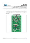
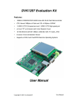
STM32L100C-Discovery Board
All lab projects will be developed for the STM32L100C-Discovery board, shown in Figure 1. This
is a low-cost, ultra-low-power development board for the STM32L100RTC6 microcontroller,
which is based on a 32-bit ARM Cortex-M3 processor. Details of the board are contained in the
STM32L100C-Discovery User Manual (available on the course web page). Details of the
STM32L100RTC6 microcontroller are contained in its data sheet and in its reference manual; these
are accessible from the course web page and from the “Books” pane of the MDK-ARM main
window.
Figure 1. STM32L100C-Discovery Board
Prior to the first lab: read and study the following in the STM32L100C-Discovery User Manual.
• Section 3: Summary of features of the Discovery board.
• Figure 2: Hardware block diagram of the board, showing the debug interface (ST-LINK),
USB connector, microcontroller, pin headers, LEDs and push buttons.
•
•
•
•
•
Figure 3: Top view of the board layout, showing pins on the two 33-pin headers (P1 and
P2) and locations of components and connectors.
Section 4.1: Features of the microcontroller (Figure 6 is its block diagram.)
Section 4.2: ST-LINK debug interface. The USB interface will be used in lab to access the
ST-LINK to the microcontroller, rather than the 6-pin connector. Refer to the jumper
settings described in Section 4.2.1. This is the default setting on the board.
Section 4.9: Lists the function(s) of each pin on the board’s two 33-pin headers (P1 and
P2). Each of the 51 GPIO (general-purpose input/output) pins has a default function
(usually simple digital input/output) and one or more alternate functions (analog I/O, timer
inputs/outputs, serial communications, etc.)
Section 6: Board schematic diagrams.
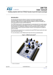
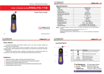
Digilent Electronics Explorer Board
The platform on which projects will be built and tested is the Digilent Electronics Explorer Board
(EEBOARD), shown in Figure 2. The EEBOARD has a breadboard area, plus connections to builtin power supplies and various debugging and test instruments (digital I/O, LEDs, switches,
oscilloscope, waveform generator, logic analyzer, etc.) The EEBOARD is controlled from a USBconnected PC via the Digilent WaveForms graphical user interface, shown in Figure 3. This
program is a free download from the Digilent web site.
Digital I/O
Connections
USB
Connector
Breadboard Area
ON/OFF
Switch
Power
Connector
Power Supply
Connections
Figure 2. Digilent Electronics Explorer Board (EEBOARD)
Figure 3. Digilent WaveForms - EEBOARD User Interface
Keil Microcomputer Development Kit for ARM Processors (MDK-ARM)
Lab projects will be created, built, downloaded to the microcontroller, debugged, and tested using
MDK-ARM (µVision5). This is an Integrated Development Environment (IDE) with installable
software packs for families of ARM-based microcontrollers. The evaluation version of this
package can be downloaded from the Keil web page for personal use. This version is limited to
program codes sizes of 32Kbytes, which is more than enough for the projects in this course. Refer
to the document Installing MDK-ARM, available on the course web page, for instructions on
downloading and installing this software. Documents describing the use of MDK-ARM to develop
and debug projects on the STM32L100C-Discovery board are also available on the course web
page.
THE LAB EXPERIMENT
The lab instructor will issue a kit to each team, containing an EEBOARD and an STM32L100CDiscovery board, to use for the duration of the semester. The kit includes a lockable case that will
hold the project board, power supply, USB cables, and other parts. These kits are not to be
removed from the lab room.
In this lab session, you will use MDK-ARM to create a project using a given C program, build
the project, download it to the microcontroller on the STM32L100C-Discovery board, and
investigate the operation of the program using various features of the MDK-ARM debug tool.
1. Begin by creating a new project, following the instructions in the document STM32L100CDiscovery Board Projects, available on the course web page. The C program to be used for
this exercise is provided at the end of this document. In the weeks that follow, a new project
should be created for each week’s lab experiment.
2. After the program has been compiled with no errors, set up the hardware and Waveforms user
interface as follows.
•
•
•
•
•
•
•
•
•
•
•
Install the STM32L100C-Discovery board on the EEBOARD breadboard area by inserting
the two 33-pin connectors into the breadboards as directed by your lab instructor. Once
inserted, please do not remove the board during the semester, to avoid bending or
breaking pins on the two connectors.
Connect one of the ground (GND) pins of connectors P1/P2 on the Discovery board to one
of the ground pins on the EEBOARD block labelled “Digital 1” at the top of the
EEBOARD (to ensure that the EEBOARD and microcontroller have a common reference
point.)
Connect GPIO pin PA0 (pin 15 of connector P1) of the Discovery board to pin 0 of the
EEBOARD “Digital 1” block. This will be configured as an LED in WaveForms to monitor
the state of the User push button on the Discovery board, which drives GPIO pin PA0 on
the microcontroller.
Connect GPIO pins PC8 and PC9 (pins 27 and 26 of connector P2) of the Discovery board
to pins 1 and 2, respectively, of the EEBOARD “Digital 1” block. These pins will be
configured as LEDs in WaveForms to monitor the states of PC8 and PC9, which drive the
blue and green LEDs, respectively, on the Discovery board.
Connect the EEBOARD to the PC with the provided USB micro AB cable.
Connect the EEBOARD power supply.
Turn the EEBOARD On-Off switch to ON.
Launch the WaveForms software on the PC.
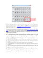
Launch the Static I/O instrument in WaveForms (Figure 4.)
By right-clicking on each (see Figure 4), configure Digital I/O pins DIO0, DIO1 and
DIO2 as LEDs. If you wish, you may remove DIO31-24, DIO23-16, and DIO15-8 from
the Static I/O display via the “Config” buttons at the left.
Connect the STM32L100C-Discovery board to the PC with the provided USB mini AB
cable. This will power on the board and allow it to be accessed via the ST-LINK interface
to the MDK-ARM debugger.
DO NOT INSERT OR REMOVE WIRES ON THE BREADBOARD WHILE POWER
IS APPLIED TO THE BOARD. This can cause voltage transients capable of damaging
the module and/or the breadboard station electronics.
Pin 0 = PA0
Pin 1 = PC8
Pin 2 = PC9
Figure 4. WaveForms Static I/O Instrument
3. After the EEBOARD has been configured and powered up, return to the main MDK-ARM
window and initiate a debug session by clicking on the Debug icon in the tool bar. (It is
assumed that the directions in STM32L100C-Discovery Board Projects,for setting up the STLINK debug interface have been followed.)
The features of the debugger are described in the document Project Debugging with MDKARM, available from the course web page. During this lab session, you should exercise these
features by performing the following operations in the debugger and recording your
observations in your lab book.
a. In the debugger Source Window, locate and click on the instruction “toggles = 0;” in your
main C program, and then look in the Disassembly window to find and record the three
assembly language instructions generated by the compiler to implement that instruction.
b. Click on the Run icon to execute the program, and record your observations as you
manipulate the user button.
c. Click on the Stop icon to halt the program, and the click the Reset icon to reset the CPU.
d. Insert a breakpoint in the program on the first instruction of the “while loop” in the main
program.
e. Execute the program, note where it halts, and then remove this breakpoint.
f. Use the Step feature to execute one instruction at a time, observing which instructions are
executed.
g. When you reach the loop that tests the user button, hold the button down to allow the
program to exit the loop on the next instruction.
h. When you reach the instruction that calls function delay(), use the Step Over feature to
execute the entire delay function as one step.
i. After returning to the main program from the delay() function, insert a breakpoint at the
first executable instruction of the delay() function (a “for” statement).
j. Click Run to resume executing the program until it reaches the new breakpoint.
k. When the program stops at the breakpoint, step through several for loops and record the
values of local variables i and j, displayed in the Call Stack + Locals Window. Also record
the values of local variables sw1 and led1 in the main program.
l. Remove the breakpoint from the delay() function.
m. Add global variable “toggles” to window Watch 1.
n. Resume executing the program, manipulate the user button, and observe the value of
variable “toggles” as the program executes.
o. Exit the debug session.
4. (Time permitting.) Modify the main program to toggle the second LED, but with this LED
OFF when the first one is ON, and vice versa. Note that the second LED is connected to
GPIO pin PC9. Then rebuild the project, and test the program in the debugger, recording
your observations.
LABORATORY STATUS REPORT AND LAB NOTEBOOK
For Lab 1, each student is to submit a separate memo-style laboratory report, as described in the
syllabus. The memo should (1) begin with a brief statement of the objectives of the lab, (2) provide
a brief summary of what was accomplished and the results that were observed, and (3) conclude
with a brief statement of what was learned, and any suggestions for the lab instructors. In future
labs, when programs are written and/or circuits designed, these should be attached to the memo,
or otherwise included.
In addition, each student should enter all pre-lab and in-lab activity in the lab notebook. Lab
notebooks will be collected from all students every two weeks, beginning with week 2.
/*====================================================*/
/* Victor P. Nelson
*/
/* ELEC 3040/3050 - Lab 1, Program 1
*/
/* Toggle LED1 while button pressed, with short delay inserted
*/
/*====================================================*/
#include "STM32L1xx.h"
/* Microcontroller information */
/* Define global variables */
int toggles;
/* number of times LED state toggled */
/*---------------------------------------------------*/
/* Initialize GPIO pins used in the program */
/*
PA0 = push button
*/
/*
PC8 = blue LED, PC9 = green LED */
/*---------------------------------------------------*/
void PinSetup () {
/* Configure PA0 as input pin to read push button */
RCC->AHBENR |= 0x01;
/* Enable GPIOA clock (bit 0) */
GPIOA->MODER &= ~(0x00000003);
/* General purpose input mode */
/* Configure PC8,PC9 as output pins to drive LEDs */
RCC->AHBENR |= 0x04;
/* Enable GPIOC clock (bit 2) */
GPIOC->MODER &= ~(0x000F0000);
/* Clear PC9-PC8 mode bits */
GPIOC->MODER
|= (0x00050000);
/* General purpose output mode*/
}
/*----------------------------------------------------------*/
/* Delay function - do nothing for about 1 second */
/*----------------------------------------------------------*/
void delay () {
int i,j,n;
for (i=0; i<100; i++) {
//outer loop
for (j=0; j<20000; j++) {
//inner loop
n = j;
//dummy operation for single-step test
}
//do nothing
}
}
/*------------------------------------------------*/
/* Main program
*/
/*------------------------------------------------*/
int main(void) {
unsigned char sw1;
//state of SW1
unsigned char led1;
//state of LED1
PinSetup();
led1 = 0;
toggles = 0;
//Configure GPIO pins
//Initial LED state
//#times LED state changed
/* Endless loop */
while (1) {
//Can also use: for(;;) {
if (led1 == 0)
GPIOC->BSRRH = 0x0100;
else
GPIOC->BSRRL = 0x0100;
sw1 = GPIOA->IDR & 0x01;
/* Wait in loop until SW1 pressed */
while (sw1 == 0) {
sw1 = GPIOA->IDR & 0x01;
}
delay();
led1 = ~led1;
toggles++;
} /* repeat forever */
}
//LED off?
//Reset PC8=0 to turn OFF blue LED
//LED on
//Set PC8=1 to turn ON blue LED
//Read GPIOA and mask all but bit 0
//Wait for SW1 = 1 on PE0
//Read GPIOA and mask all but bit 0
//Time delay for button release
//Complement LED1 state
//Increment #times LED toggled