1
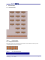
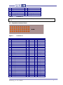
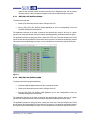
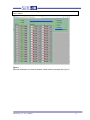
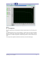
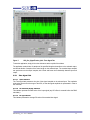
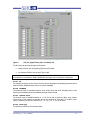
SR3_Analog_32
User’s Manual
by
with the collaboration of
March 2nd 2012
1040, avenue Belvédère, suite 215
Québec (Québec) G1S 3G3 Canada
Tél.: (418) 686-0993 Fax: (418) 686-2043
1
INTRODUCTION ______________________________________________ 4
2
TECHNICAL DATA ____________________________________________ 4
2.1
Analog Inputs __________________________________________________________________ 4
2.2
Analog Outputs ________________________________________________________________ 5
2.3
FPGA IOs _____________________________________________________________________ 5
3
CONNECTOR MAPS ___________________________________________ 6
3.1
Channel Locations ______________________________________________________________ 6
3.2
Analog Connector Pinouts _______________________________________________________ 6
3.3
Expansion Connector Pinout _____________________________________________________ 7
3.3.1
Bus Switches _______________________________________________________________ 8
3.3.2
Power Supply Pins ___________________________________________________________ 9
4
INSTALLATION _______________________________________________ 9
4.1
Software Installation ____________________________________________________________ 9
4.2
Development Resources _________________________________________________________ 9
4.3
FPGA Configuration ____________________________________________________________ 9
4.4
Mating SR3_Analog_32 to the DSP board ___________________________________________ 9
5
SOFTWARE __________________________________________________ 9
5.1
Self-Test Application ____________________________________________________________ 9
5.1.1
SR3_PRO_A32_SelfTest_Simple ______________________________________________ 10
5.1.2
SR3_PRO_A32_SelfTest_LpBk _______________________________________________ 10
5.2
Demo Application _____________________________________________________________ 12
5.2.1
Time Signal Tab ___________________________________________________________ 13
5.2.2
Sxx Tab __________________________________________________________________ 14
5.2.3
Acquisition Set-Up Tab ______________________________________________________ 14
5.3
SR3_Analog_32 Drivers and Example-Code ________________________________________ 16
5.3.1
Overview _________________________________________________________________ 16
5.3.2
User-Accessible Structures and Functions________________________________________ 16
5.3.3
Used Resources ____________________________________________________________ 17
5.3.4
Restrictions _______________________________________________________________ 18
SR3-Analog_32 - User’s Manual
3
1
Introduction
SR3_Analog_32 is a 32-input/32-output analog board that is designed to work with the
SignalRanger_mk3_Pro DSP board, in applications such as acoustics and vibration beamforming, and
multi-channel control.
It features Sigma-Delta Analog Interface Circuits (1 AIC = 1 ADC + 1 DAC), with bit-depth up to 32 bits
and sampling frequencies up to 96 kHz. It has one separate ADC and DAC per channel. Each input
path includes differential inputs, as well as electret-microphone inputs
SR3_Analog_32 carries over the FPGA IOs of SignalRanger_mk3_Pro, through bus switches for
improved reliability and 5V-tolerance.
2
Technical Data
2.1
Analog Inputs
Parameter
Number of channels
Value
32
Sampling Rate
6 kHz, 12 kHz, 24 kHz, 32 kHz, 48 kHz, 96 kHz
Resolution
16, 20, 24 or 32 bits
Gain
0 dB to 47.5 dB
(0.5dB resolution)
Noise
65 µVRMS (typ.)
18 µVRMS (typ.)
@ 0 dB gain
@ +18 dB gain
Signal to Noise Ratio
90.4 dB (typ.)
@ 48 kHz, differential input, 0 dB gain, A-filter
Bandwidth
Up to 48 kHz
Input types
•
•
Coupling
DC
AC (1Hz Cutoff)
Dynamic Range
(differential inputs)
+-2.8V
+-5.6V
@ 0dB gain
Dynamic Range
(electret-microphone inputs)
+-0.9V
@ 0 dB gain
Input Impedance
20 kΩ - Single-Ended
40 kΩ - Differential
Anti-Aliasing Filter
Integral:
Filter A: best noise
Filter B:
Differential
Electret-Microphone
Differential Inputs
Electret Microphone Inputs
Single Ended
Differential
22-sample group-delay
17-sample group-delay
Table 1
SR3-Analog_32 - User’s Manual
4
Note:
2.2
Not all combinations of Sampling Frequency, Bit-Width and Channel Count are possible.
Analog Outputs
Parameter
Number of channels
Value
32
Sampling Rate
6 kHz, 12 kHz, 24 kHz, 32 kHz, 48 kHz, 96 kHz
Resolution
16, 20, 24 or 32 bits
Noise
(24 kHz bandwidth)
30 µVRMS (typ.)
Signal to Noise Ratio
97 dB typ
@ 48 kHz, A-filter
Bandwidth
Up to 48 kHz
Input types
Single Ended
Coupling
DC
Dynamic Range
+-2.8V
Output Impedance
50 Ω
Source/Sink Ability
25 mA
Anti-Aliasing Filter
Integral:
Filter A: best noise
Filter B:
22-sample group-delay
17-sample group-delay
Table 2
Note:
2.3
Not all combinations of Sampling Frequency, Bit-Width and Channel Count are possible.
FPGA IOs
Parameter
Number of IOs
Value
59
Protection
All IOs are seen through switches which isolate the FPGA from external logic if
either SignalRanger_mk3_Pro is unpowered or Presence signal is not active
IO Level
3.3V CMOS (5V-tolerant inputs)
Table 3
SR3-Analog_32 - User’s Manual
5
3
3.1
Connector Maps
Channel Locations
Figure 1
3.2
Channel Locations
Analog Connector Pinouts
Each analog connector (JAi, JBi) supports a pair of channels. The even channel is on the even pin row.
The following odd channel is on the odd pin row.
Figure 2
No
1
JAi – JBi connector pinouts
Function
Out_1
SR3-Analog_32 - User’s Manual
No
2
Function
Out_0
6
3
5
7
9
11
13
Gnd
+In_1
-In_1
Gnd
Electret_Mic_1
Electret_Polarization Voltage
Table 4
4
6
8
10
12
14
Gnd
+In_0
-In_0
Gnd
Electret_Mic_0
Electret_Polarization Voltage
Connector J1
Note: The table above shows channels 0 and 1. The pinout is the same for channels 2 and 3, 4 and
5…etc.
3.3
Expansion Connector Pinout
Figure 3
No
1
4
7
10
13
16
19
22
25
28
31
34
37
40
43
46
49
52
55
58
61
64
67
70
73
76
79
82
Connector J1
Function
+5V
+1.8V
NC
-3.3V
NC
NC
NC
NC
NC
NC
UART_Rx
NC
FPGA_17
FPGA_14
FPGA_12
FPGA_10
FPGA_7
FPGA_5
FPGA_2
FPGA_141
FPGA_137
FPGA_68
FPGA_70
FPGA_74
FPGA_77
FPGA_79
FPGA_82
FPGA_84
SR3-Analog_32 - User’s Manual
No
2
5
8
11
14
17
20
23
26
29
32
35
38
41
44
47
50
53
56
59
62
65
68
71
74
77
80
83
Function
Gnd
Gnd
Gnd
Gnd
Gnd
Gnd
Gnd
Gnd
Gnd
Gnd
Gnd
Gnd
Gnd
Gnd
Gnd
Gnd
Gnd
Gnd
Gnd
Gnd
Gnd
Gnd
Gnd
Gnd
Gnd
Gnd
Gnd
Gnd
No
3
6
9
12
15
18
21
24
27
30
33
36
39
42
45
48
51
54
57
60
63
66
69
72
75
78
81
84
Function
+2.5V
+1.2V
+3.3V
DSP_Reset
NC
NC
NC
NC
NC
NC
UART_Tx
Presence
NC
NC
NC
FPGA_8
FPGA_6
FPGA_4
FPGA_1
FPGA_140
FPGA_135
FPGA_69
FPGA_73
FPGA_76
FPGA_78
FPGA_80
FPGA_83
FPGA_85
7
85
88
91
94
97
100
103
106
109
112
115
118
121
124
127
130
FPGA_86
FPGA_89
FPGA_92
FPGA_95
FPGA_97
FPGA_99
FPGA_102
FPGA_104
FPGA_107
FPGA_112
FPGA_116
FPGA_119
FPGA_123
FPGA_125
FPGA_130
FPGA_132
Table 5
86
89
92
95
98
101
104
107
110
113
116
119
122
125
128
131
Gnd
Gnd
Gnd
Gnd
Gnd
Gnd
Gnd
Gnd
Gnd
Gnd
Gnd
Gnd
Gnd
Gnd
Gnd
Gnd
87
90
93
96
99
102
105
108
111
114
117
120
123
126
129
132
FPGA_87
FPGA_90
FPGA_93
FPGA_96
FPGA_98
FPGA_100
FPGA_103
FPGA_105
FPGA_108
FPGA_113
FPGA_118
FPGA_122
FPGA_124
FPGA_129
FPGA_131
FPGA_HS_EN
Connector J1
3.3.1 Bus Switches
The expansion signals on J1 are connected to the corresponding FPGA and DSP pins on
Signal_Ranger_mk3_Pro through bus switches.
A Presence input is provided on J1 pin 36. This input is used to activate the bus switches that otherwise
isolate all the signals of J1 from the DSP board.
The bus switches provide two functions:
•
They isolate the DSP board from a user board connected on J1 when one board is powered but
not the other. This is essential because in the absence of the switches, line drivers on one board
could be driving unpowered input stages on the other, which could damage them.
•
They provide level translation between the user-board, which can drive levels up to 5V and inputs
on the DSP board that are not 5V-tolerant. In short, the switches make the DSP board inputs 5Vtolerant.
To provide the first function, the switches should only be activated (placed in low-impedance) when the
user daughter board is powered. The Presence input serves that purpose. This input is normally pulledup by a 10 kΩ resistor on SR3_Analog_32, which keeps the switches open. The Presence pin should
be pulled low by an active open-drain driver on the user’s daughter board. That driver should only pull
low and close the switches, when the daughter board is properly powered. Pulling Presence low when
the user’s daughter board is not properly powered (before it is powered or after it is un-powered)
exposes input stages on the user’s board to damage inflicted by FPGA pins that may be configured as
outputs. Depending on how the FPGA is configured at the time it may not be a problem. For instance if
the FPGA is not configured, its IOs are floating and will not drive any current. In this case, Presence
may be permanently tied to ground. Pulling Presence low when the user’s daughter board is properly
powered but the DSP board is not DOES NOT EXPOSE the FPGA inputs to damage that may be
inflicted by line drivers on the user’s daughter board. This is because the switches are open whenever
the DSP board is unpowered.
The level-translation function is provided automatically whenever the switches are activated (whenever
Presence is low).
SR3-Analog_32 - User’s Manual
8
3.3.2 Power Supply Pins
3.3.2.1
+5V
This is the same supply that is brought to the 5V power connector J3. The maximum current that may
be drawn from this pin is 200 mA.
3.3.2.2
Other Supply Pins
It is not recommended to draw power from any of the other supply pins.
4
Installation
4.1
Software Installation
Unzip the SR3_Applications_Installer_Vxxx.zip file and run setup.exe. This installs the following:
•
A directory SR3_Applications in C:\Program Files (if it did not exist already) containing
documentation, LabVIEW libraries, Test applications, DSP code examples…etc.
•
The driver for the SignalRanger_mk3_Pro DSP board
•
Shortcuts to compiled test applications and documentation.
4.2
Development Resources
LabVIEW developers can find all the relevant resources in the following distribution:
SR3_DDCI_Library_Distribution_Vxxx.zip. Those development resources include Vis and DSP code
that are specific to the SR3_Analog_32 IO board. See the SignalRanger_mk3_Pro_UsersManual for
more information about those development resources.
4.3
FPGA Configuration
The FPGA on the DSP board is not used to manage the ADCs and DACs on SR3_Analog_32. The
user has complete freedom in the logic that is implemented on the FPGA
Mating SR3_Analog_32 to the DSP board
4.4
When SR3_Analog_32 is purchased with a DSP board the two boards are already mated. If not
SR3_Analog_32 must be mated to the DSP board prior to powering-up. Never attempt to mate the two
boards while the DSP board is powered.
5
Software
5.1
Self-Test Application
Two applications are provided to perform diagnostics on the SR3_Analog_32 board:
•
SR3_PRO_A32_SelfTest_Simple
This application tests all the digital aspects of the
board, including the AICs. That application runs quickly and does not require any loopback on
the analog connectors. It can be performed at any time.
•
SR3_PRO_A32_SelfTest_LpBk
This application additionally tests the analog
performance of the input and output channels. It requires special loopback connectors to be
inserted into the analog connectors before the test. The loopback connectors connect the
SR3-Analog_32 - User’s Manual
9
output of each channel to both the positive terminal of the differential input, and the electret
microphone input. It also connects the negative terminal of the differential input to ground.
5.1.1 SR3_PRO_A32_SelfTest_Simple
To perform the simple test:
•
Power-up the board and connect it to the USB port of the PC.
•
Run the SR3_PRO_A32_SelfTest_Simple application (or run the corresponding VI from the
LabVIEW development environment).
The application performs all the tests in sequence and presents the results in the form of a green
(good) or red (not-good) indicator. When the board is operating properly all indicators should be green.
The application presents a dialog just before running the FPGA test. That test configures the FPGA
pins as outputs and drives patterns of zeros and ones on the pins. If the board is connected to external
user logic that test could damage such logic. In such a situation we recommend to skip the FPGA test.
Figure 4
5.1.2 SR3_PRO_A32_SelfTest_LpBk
To perform this more thorough loopback test:
•
Insert the loopback adapter boards into all the analog connectors.
•
Power-up the board and connect it to the USB port of the PC.
•
Run the SR3_PRO_A32_SelfTest_LpBk application (or run the corresponding VI from the
LabVIEW development environment).
The application performs all the tests in sequence and presents the results in the form of a green
(good) or red (not-good) indicator. When the board is functional all indicators should be green.
The application presents a dialog just before running the FPGA test. That test configures the FPGA
pins as outputs and drives patterns of zeros and ones on the pins. If the board is connected to external
user logic that test could damage such logic. In such a situation we recommend to skip the FPGA test.
SR3-Analog_32 - User’s Manual
10
Note: The channel indicators are only green on the channels that have the loopback board (channel
0 and 1 below).
Figure 5
When the Detail button of a channel is pressed, a detail window is presented (see Figure 6).
SR3-Analog_32 - User’s Manual
11
Figure 6
5.2
Demo Application
SR3_PRO_SignalTracker_A32 demonstrates the features and performance of the SR3_Analog_32 IO
board.
The application allows the user to send test signals to a selected output, and monitor the sampled
signal on a selected input. Analog inputs are displayed both in terms of time signals, as well as
instantaneous or averaged energy spectra. Averaged energy spectra are useful to assess the input
noise.
The front-panel of the application is divided into several tabs, one for each functional group.
SR3-Analog_32 - User’s Manual
12
Figure 7
SR3_Pro_SignalTracker_A32 - Time Signal Tab
To start the application, simply click on the white arrow at the top-left of the window.
The application sends blocks of samples of the specified length and waveform to the selected output,
and records blocks of samples of the same length on the selected input. The recorded input samples
are synchronous to the output samples, with a fixed and known time relationship between input and
output.
5.2.1 Time Signal Tab
5.2.1.1
Time Indicator
The Time-Signal tab presents a time plot of the signal sampled on the selected input. The amplitude
scale takes into account the range of the ADC, so that the signal amplitude is represented in Volts at
the connector.
5.2.1.2
AC estimate (Vrms) Indicator
This indicator presents the RMS value of the input signal (any DC offset is removed before the RMS
calculation).
5.2.1.3
DC (V) Indicator
This indicator presents the average DC value of the recorded time signal.
SR3-Analog_32 - User’s Manual
13
5.2.2 Sxx Tab
Figure 8
5.2.2.1
SR3_Pro_SignalTracker_A32 - Sxx Tab
Spectrum Indicator
The Spectrum indicator presents the instantaneous or averaged power spectrum of the input sampled
block.
5.2.2.2
Average Control
To average the power-spectrum, simply place the Average control in the ON position.
5.2.2.3
Reset Average Button
The Reset Average button resets the averaging process.
5.2.2.4
Time Window selector
An optional weighting window can be chosen from the Time-Window list.
5.2.2.5
Graph and Zoom Controls
Graph controls can be used to change the zoom factor. By default the plot is auto-scaled in X and Y,
which is indicated by the closed locks beside each scale name. To disable auto-scale, simply press the
lock button.
5.2.3 Acquisition Set-Up Tab
The Acquisition Set-Up tab presents the various controls for the acquisition set-up.
SR3-Analog_32 - User’s Manual
14
Figure 9
SR3_Pro_SignalTracker_A32 – AIC Setup Tab
The AIC Setup tab presents two types of information:
•
Global Controls, such as Sampling Frequency or Bit-Width
•
Per-Channel Controls, such as Input Type or Gain
Note: Not all combinations of Sampling Frequency, Bit-Width and Channel Count are possible. When
a combination is not allowed, a dialog is presented to prompt the user to change the configuration.
5.2.3.1
FS
The sampling frequency can be set from 6 kHz to 96 kHz. Be aware that sampling frequencies below
48 kHz introduce additional output noise in the 24 kHz bandwidth.
5.2.3.2
Bit-Width
The sample bit-width is selectable between 16-bit, 20-bit, 24-bit and 32-bit. Bit-widths above 16-bit
require more bandwidth and are incompatible with large channel counts.
5.2.3.3
Channel Count
The channel count is selectable between 8, 12 16, 20, 24 and 32 channels. When using channel
counts below 32 the channels in operation are the first channels of each bank. For instance, when
using 12 channels, the channel numbers are: 0, 1, 2, 3, 4, 5, 16, 17, 18, 19, 20 and 21.
5.2.3.4
Filter Type
The selection provides two reconstruction filters:
SR3-Analog_32 - User’s Manual
15
•
Filter A has a longer group-delay (22 samples on inputs and outputs), but provides better
rejection of out-of-band components, and better noise figures.
•
Filter B provides a shorter group-delay (17 samples on inputs and outputs).
5.2.3.5
Gain dB
The input gain can be adjusted individually on each input from 0 dB to +47.5 dB. A higher gain provides
a lower noise level, but also reduces the dynamic range correspondingly.
5.2.3.6
Input Type
Each channel can be set for a differential input or an electret microphone input.
5.3
SR3_Analog_32 Drivers and Example-Code
5.3.1 Overview
A DSP driver for the analog I/Os is provided, together with the DSP code of the
SR3_PRO_SignalTracker_A32 demo application that uses that driver. An empty shell project is also
provided for users who want to develop their own DSP application.
Source code for the analog IO driver resides in the folder named SR3PRO_A32Driver.
The source code for the SR3_PRO_SignalTracker_A32 demo application resides in the folder named
SR3_PRO_A32_SignalTracker
The source code for the empty shell project resides in the folders named SR3_PRO_A32_IOShell
The shell project constitutes an excellent starting point for developing DSP code that uses the
SR3_Analog_32 board.
The driver has been optimized in assembly language, but can be used in either C, or assembly
language. It takes the form of a DSP object library SR3PRO_AIC3204Driver.lib. The driver contains Ccallable functions to configure and use the analog IOs. A function named Dataprocess() is provided in
C, where developers can conveniently place their own analog I/O processing code.
The driver uses the DMA to communicate with the analog IOs for maximum efficiency.
5.3.2 User-Accessible Structures and Functions
The SR3PRO_AIC3204Driver.lib library defines and allocates the following user-accessible structures,
functions and variables (all defined in SR3PRO_AIC3204_AICDriver.h):
5.3.2.1
McBSP_Regs[4]
This vector contains the configuration data for the McBSP. We suggest using the VI
SR3Pro_AIC3204_Generate_AICRegistersApp.vi or the .exe version of this VI to generate the content
of this vector.
5.3.2.2
AIC3204_Regs[1344]
This vector contains the configuration data for the AICs. We suggest using the VI
SR3Pro_AIC3204_Generate_AICRegistersApp.vi or the .exe version of this VI to generate the content
of this vector.
5.3.2.3
Input-Output AIC Structure
The structure is allocated by the driver library as follows, and it is designed to contain the input and
output samples to/from the AICs. The user DSP code has one complete sampling period to execute the
SR3-Analog_32 - User’s Manual
16
Dataprocess() function. If the function is not completed within a sampling period input samples are
overwritten by the new samples, and the previous output samples are sent to the AICs.
BIN0 and BOUT0 represents the first ADC/DAC bank and BIN1 and BOUT1 represents the second
ADC/DAC bank. Following the data format used, the user can select the I32, I24, I20 and I16 member
of the union for input and output data.
Note: The structure is allocated automatically as a consequence of including the driver library within
the user DSP code. There is no need for the user DSP code to allocate this structure.
5.3.2.4
StartAIC3204();
This function configures the analog IOs and starts the conversion process. It has no arguments. It uses
the configuration values found in the McBSP_Regs[4] and AIC3204_Regs[1344] variables and
configures the analog IOs accordingly. These variables must be initialized prior to calling
StartAIC3204() (use the dedicated VI or application to do that). After the execution of this function, the
user-defined processing function called Dataprocess() starts being triggered at each sampling period.
5.3.2.5
StopAIC3204();
This function stops the AIC conversion process. After the execution of this function, the user-defined
Dataprocess() function is no longer triggered.
5.3.2.6
Dataprocess()
This function is declared by the AIC driver library, but must be provided by the user. It usually contains
the DSP code that reads the input samples from the AIC structure, performs the signal processing
between the inputs and outputs and writes the output samples to the AIC structure. The _Dataprocess
symbol must be declared using the .global directive when the code is written in assembler
Note: The Dataprocess() function is a standard function and no special protection is required since
the acquisition driver itself protects the context.
Just before the entry into Dataprocess() the global interrupt mask (CSR) is set. Therefore all interrupts
are disabled. The local mask registers are saved on the stack and restored after the execution of
Dataprocess(). If the user needs to unmask another interrupt within Dataprocess() they must be mindful
of timing issues. The execution of Dataprocess() must complete within one sampling period. Also all the
interrupt masks are restored to their state prior to the execution of Dataprocess() at the function’s exit.
Therefore any interrupt explicitly enabled by user-code in Dataprocess(), that was not enabled before
entry, is disabled at exit.
5.3.3 Used Resources
The AIC driver uses the following hardware resources:
•
DMA channels 2 to 5 are used by the driver.
•
Reload DMA parameters 66 to 73 are used by the driver.
•
INT5, linked to DMA channel 3 (region 0) is used by the driver.
•
GPIO22 and 23 are used to control the reset of the AIC and I2C switches.
•
McBSP0 and McBSP1 are used by the AIC driver.
•
The I2C controller is set at 372 kHz and used by the AIC driver.
SR3-Analog_32 - User’s Manual
17
•
Clkout0 is connected to the AIC Master-Clocks and set to 24 MHz.
•
The driver uses 4576 bytes of code and 2122 bytes of data.
5.3.4 Restrictions
When developing C or assembly code using the AIC driver, the following restrictions apply:
•
The user-defined I/O processing function Dataprocess() must be present in the user code. The
AIC driver does the full context save before calling Dataprocess(). If the function is written in
assembler, the _Dataprocess symbol must be defined using the .global directive.
•
All C-accessible symbols and labels defined in the SR3PRO_AIC3204Driver.lib library must have
a _ prefix when used in assembly language.
•
The INT5, linked to the DMA channel 3 (region 0), the GPIO22 and 23, the DMA channels 2 to 5
and 66 to 73 are used by the AIC driver. The vectors for these interrupts must be properly
declared. See the SR3_PRO_SignalTracker_A32 or SR3_PRO_A32_IOShell DSP code projects
for examples of a correct implementation of vectors.asm.
SR3-Analog_32 - User’s Manual
18